US20170269635A1 - Display unit and its manufacturing method - Google Patents
Display unit and its manufacturing methodDownload PDFInfo
- Publication number
- US20170269635A1 US20170269635A1US15/612,718US201715612718AUS2017269635A1US 20170269635 A1US20170269635 A1US 20170269635A1US 201715612718 AUS201715612718 AUS 201715612718AUS 2017269635 A1US2017269635 A1US 2017269635A1
- Authority
- US
- United States
- Prior art keywords
- display unit
- panel
- light emitting
- display
- touch panel
- Prior art date
- Legal status (The legal status is an assumption and is not a legal conclusion. Google has not performed a legal analysis and makes no representation as to the accuracy of the status listed.)
- Granted
Links
Images


Classifications
- G—PHYSICS
- G06—COMPUTING OR CALCULATING; COUNTING
- G06F—ELECTRIC DIGITAL DATA PROCESSING
- G06F3/00—Input arrangements for transferring data to be processed into a form capable of being handled by the computer; Output arrangements for transferring data from processing unit to output unit, e.g. interface arrangements
- G06F3/01—Input arrangements or combined input and output arrangements for interaction between user and computer
- G06F3/03—Arrangements for converting the position or the displacement of a member into a coded form
- G06F3/041—Digitisers, e.g. for touch screens or touch pads, characterised by the transducing means
- G06F3/0416—Control or interface arrangements specially adapted for digitisers
- G06F3/0418—Control or interface arrangements specially adapted for digitisers for error correction or compensation, e.g. based on parallax, calibration or alignment
- G—PHYSICS
- G06—COMPUTING OR CALCULATING; COUNTING
- G06F—ELECTRIC DIGITAL DATA PROCESSING
- G06F1/00—Details not covered by groups G06F3/00 - G06F13/00 and G06F21/00
- G06F1/16—Constructional details or arrangements
- G06F1/1613—Constructional details or arrangements for portable computers
- G06F1/1626—Constructional details or arrangements for portable computers with a single-body enclosure integrating a flat display, e.g. Personal Digital Assistants [PDAs]
- G—PHYSICS
- G06—COMPUTING OR CALCULATING; COUNTING
- G06F—ELECTRIC DIGITAL DATA PROCESSING
- G06F1/00—Details not covered by groups G06F3/00 - G06F13/00 and G06F21/00
- G06F1/16—Constructional details or arrangements
- G06F1/1613—Constructional details or arrangements for portable computers
- G06F1/1633—Constructional details or arrangements of portable computers not specific to the type of enclosures covered by groups G06F1/1615 - G06F1/1626
- G06F1/1637—Details related to the display arrangement, including those related to the mounting of the display in the housing
- G06F1/1643—Details related to the display arrangement, including those related to the mounting of the display in the housing the display being associated to a digitizer, e.g. laptops that can be used as penpads
- G—PHYSICS
- G06—COMPUTING OR CALCULATING; COUNTING
- G06F—ELECTRIC DIGITAL DATA PROCESSING
- G06F1/00—Details not covered by groups G06F3/00 - G06F13/00 and G06F21/00
- G06F1/16—Constructional details or arrangements
- G06F1/1613—Constructional details or arrangements for portable computers
- G06F1/1633—Constructional details or arrangements of portable computers not specific to the type of enclosures covered by groups G06F1/1615 - G06F1/1626
- G06F1/1637—Details related to the display arrangement, including those related to the mounting of the display in the housing
- G06F1/1652—Details related to the display arrangement, including those related to the mounting of the display in the housing the display being flexible, e.g. mimicking a sheet of paper, or rollable
- G—PHYSICS
- G06—COMPUTING OR CALCULATING; COUNTING
- G06F—ELECTRIC DIGITAL DATA PROCESSING
- G06F1/00—Details not covered by groups G06F3/00 - G06F13/00 and G06F21/00
- G06F1/16—Constructional details or arrangements
- G06F1/1613—Constructional details or arrangements for portable computers
- G06F1/1633—Constructional details or arrangements of portable computers not specific to the type of enclosures covered by groups G06F1/1615 - G06F1/1626
- G06F1/1684—Constructional details or arrangements related to integrated I/O peripherals not covered by groups G06F1/1635 - G06F1/1675
- G06F1/169—Constructional details or arrangements related to integrated I/O peripherals not covered by groups G06F1/1635 - G06F1/1675 the I/O peripheral being an integrated pointing device, e.g. trackball in the palm rest area, mini-joystick integrated between keyboard keys, touch pads or touch stripes
- G06F1/1692—Constructional details or arrangements related to integrated I/O peripherals not covered by groups G06F1/1635 - G06F1/1675 the I/O peripheral being an integrated pointing device, e.g. trackball in the palm rest area, mini-joystick integrated between keyboard keys, touch pads or touch stripes the I/O peripheral being a secondary touch screen used as control interface, e.g. virtual buttons or sliders
- G—PHYSICS
- G06—COMPUTING OR CALCULATING; COUNTING
- G06F—ELECTRIC DIGITAL DATA PROCESSING
- G06F3/00—Input arrangements for transferring data to be processed into a form capable of being handled by the computer; Output arrangements for transferring data from processing unit to output unit, e.g. interface arrangements
- G06F3/01—Input arrangements or combined input and output arrangements for interaction between user and computer
- G06F3/048—Interaction techniques based on graphical user interfaces [GUI]
- G06F3/0487—Interaction techniques based on graphical user interfaces [GUI] using specific features provided by the input device, e.g. functions controlled by the rotation of a mouse with dual sensing arrangements, or of the nature of the input device, e.g. tap gestures based on pressure sensed by a digitiser
- G06F3/0488—Interaction techniques based on graphical user interfaces [GUI] using specific features provided by the input device, e.g. functions controlled by the rotation of a mouse with dual sensing arrangements, or of the nature of the input device, e.g. tap gestures based on pressure sensed by a digitiser using a touch-screen or digitiser, e.g. input of commands through traced gestures
- H01L27/323—
- H—ELECTRICITY
- H10—SEMICONDUCTOR DEVICES; ELECTRIC SOLID-STATE DEVICES NOT OTHERWISE PROVIDED FOR
- H10K—ORGANIC ELECTRIC SOLID-STATE DEVICES
- H10K59/00—Integrated devices, or assemblies of multiple devices, comprising at least one organic light-emitting element covered by group H10K50/00
- H10K59/40—OLEDs integrated with touch screens
- C—CHEMISTRY; METALLURGY
- C09—DYES; PAINTS; POLISHES; NATURAL RESINS; ADHESIVES; COMPOSITIONS NOT OTHERWISE PROVIDED FOR; APPLICATIONS OF MATERIALS NOT OTHERWISE PROVIDED FOR
- C09K—MATERIALS FOR MISCELLANEOUS APPLICATIONS, NOT PROVIDED FOR ELSEWHERE
- C09K2323/00—Functional layers of liquid crystal optical display excluding electroactive liquid crystal layer characterised by chemical composition
Definitions
- the present inventionrelates to a display unit having a touch panel and its manufacturing method, and more particularly such a display unit using organic light emitting devices and its manufacturing method.
- a so-called touch screenwherein a touch panel is mounted to a display panel using a CRT (Cathode Ray Tube) or a liquid crystal is widely used in banks, stations and the like. Additionally, a compact touch screen is adopted for a PDA (Personal Digital Assistant), a portable terminal and the like.
- CTRCathode Ray Tube
- PDAPersonal Digital Assistant
- a general touch panel used for conventional touch screensis, for example, has a structure wherein a glass substrate and a plastic film are layered.
- a glass substrate sideis placed opposite to a display panel, so that a plastic film side becomes an operation face.
- a voidis provided between a glass substrate of the touch panel and the liquid crystal display panel.
- a touch panel having a structure wherein two plastic films are layered(hereinafter referred to as “flexible touch panel”) has been developed, and this flexible touch panel is expected as what allows the PDA, the portable terminal and the like to become further thinner and lighter.
- a flexible touch panelhas no rigidity itself since it has no glass substrate, so that the flexible touch panel should be supported by bonding a display panel thereto. Therefore, there is a problem that the flexible touch panel cannot be provided with a void between itself and the display panel as in a touch screen of a conventional liquid crystal display panel, so that it is difficult to mount the flexible touch panel to the liquid crystal display panel.
- the can sealing structureis a structure wherein an adhesive is applied to the rim part of a rear panel, a sealing can made of metals or glass is bonded thereto, and a getter material such as calcium is enclosed in a space between the rear panel and the sealing can.
- a getter materialsuch as calcium
- a display unitcomprises a display panel including a substrate wherein display devices are formed; and a touch panel which is directly bonded to the whole face of the display panel with an adhesive layer in between, and which detects contact with a finger or a pen.
- a method of manufacturing the display unit according to the inventionincludes the steps of forming the display panel including the substrate wherein the display devices are formed; and directly bonding a whole face of the touch panel which detects contact with a finger or a pen and the display panel together with the adhesive layer in between.
- the whole faces of the touch panel and the display panelare directly bonded together with the adhesive layer in between. Therefore, there is no void between the touch panel and the display panel, so that a thickness of the display unit is reduced.
- the display panelhas a sealing substrate which is placed opposite to a display device side of the substrate, and the whole faces of the substrate and the sealing substrate are bonded together with the adhesive layer in between.
- a suitable touch panelis, for example, a touch panel having a structure wherein two plastic films in which respective transparent electrodes are formed are layered so that the transparent electrodes are placed opposite to each other. The reason of it is that thickness and weight of the display unit is further reduced. Another reason of it is that even when the touch panel is such a touch panel with low rigidity, the touch panel is supported by the display panel, so that when distortion or bending is generated in the plastic film due to contact with a finger or a pen, such distortion or bending is restrained or recovered by the display panel.
- a suitable display deviceis an organic light emitting device, which has an organic layer including a light emitting layer between a first electrode and a second electrode, and which extracts lights generated in the light emitting layer from the second electrode side.
- the touch panel and the display panelare directly bonded without providing a void between the touch panel and the display panel since the organic light emitting device has no blooming phenomenon as in the liquid crystal. Therefore, by the structure of the invention, high image quality can be realized.
- FIG. 1is a cross sectional view showing a construction of a display unit according to a first embodiment of the invention
- FIG. 2is an enlarged cross sectional view showing a construction of an organic layer in organic light emitting devices illustrated in FIG. 1 ;
- FIG. 3is an enlarged cross sectional view showing a construction of an organic layer in an organic light emitting device illustrated in FIG. 1 ;
- FIGS. 4A and 4Bare cross sectional views showing a method of manufacturing the display unit illustrated in FIG. 1 in the order of processes;
- FIG. 5is a cross sectional view showing a process following FIGS. 4A and 4B ;
- FIGS. 6A and 6Bare explanation drawings showing a process following FIG. 5 ;
- FIGS. 7A to 7Care explanation drawings showing a method of manufacturing a display unit according to a modification of the invention.
- FIG. 8is a cross sectional view showing a construction of a display unit according to a second embodiment of the invention.
- FIGS. 9A and 9Bare explanation drawings showing a method of manufacturing the display unit according to the modification of the invention.
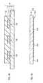
- FIG. 1shows a cross sectional structure of a display unit according to a first embodiment of the invention.
- This display unitis used as an ultrathin organic light emitting color display unit or the like, and, for example, a touch panel 20 is bonded to a whole face of a display panel 10 by an adhesive layer 30 .
- a driving panel 40 and a sealing panel 50are placed opposite, and whole faces of both the panels 40 and 50 are bonded by an adhesive layer 60 .
- the driving panel 40has a structure wherein, for example, an organic light emitting device 10 R which emits red lights, an organic light emitting device 10 G which emits green lights, and an organic light emitting device 10 B which emits blue lights are provided in order in a matrix state as a whole, on a driving substrate 11 made of an insulating material such as glass.
- the driving substrate 11is provided with a protective film (passivation film) 11 A to prevent moisture and the like from intruding into the organic light emitting devices 10 R, 10 G, and 10 B.
- a first electrode 12 as an anode, an organic layer 13 , and a second electrode 14 as a cathodeare layered in this order from the driving substrate 11 side.
- the protective film 11 Ais formed on the second electrode 14 .
- the first electrode 12also has a function as a reflection layer, and it is desirable that the first electrode 12 has a reflectance as high as possible in order to improve light emitting efficiency.
- materials to make the first electrode 12include simple substances or alloys of metal elements with high work function, such as platinum (Pt), gold (Au), silver (Ag), chromium (Cr), tungsten (W) and the like.
- a thickness of the first electrode 12 in the layer direction(hereinafter simply referred to as “thickness”) is preferably from 100 nm to 300 nm.
- AgPdCu alloywhose main component is silver, and which contains palladium (Pd) of 0.3 wt % to 1 wt % and copper (Cu) of 0.3 wt % to 1 wt % can be cited.
- FIG. 2shows an enlarged view of a construction of the organic layer 13 in the organic light emitting devices 10 R and 10 B.
- the organic layer 13 of the organic light emitting devices 10 R and 10 Bhas a structure wherein an electron hole injection layer 13 A, an electron hole transport layer 13 B, a light emitting layer 13 C, an electron transport layer 13 D, and an electron injection layer 13 E are layered in this order from the first electrode 12 side.
- a function of the electron hole injection layer 13 A and the electron hole transport layer 13 Bis to improve efficiency to inject electron holes into the light emitting layer 13 C.
- a function of the light emitting layer 13 Cis to produce lights by current injection.
- a function of the electron transport layer 13 D and the electron injection layer 13 Eis to improve efficiency to inject electrons into the light emitting layer 13 C.
- the electron hole injection layer 13 A of the organic light emitting device 10 Rhas a thickness of about 30 nm, and made of 4,4′,4′′-tris(3-methylphenyl phenyl amino)tri-phenyl amine (MTDATA).
- the electron hole transport layer 13 B of the organic light emitting device 10 Rhas a thickness of about 30 nm, and made of bis [(N-naphthyl)-N-phenyl]benzidine ( ⁇ -NPD).
- the light emitting layer 13 C of the organic light emitting device 10 Rhas a thickness of about 50 nm, and made of 2,5-bis [4-[N-(4-methoxyphenyl)-N-phenylamino]]stilbenzene-1,4-dica-bonitrile (BSB).
- the electron transport layer 13 D of the organic light emitting device 10 Rhas a thickness of about 30 nm, and made of 8-quinolinol aluminum complex (Alq).
- the electron injection layer 13 E of the organic light emitting device 10 Rfor example, has a thickness of 1 nm, and made of lithium fluoride (LiF).
- the electron hole injection layer 13 A of the organic light emitting device 10 Bhas a thickness of about 30 nm, and made of MTDATA.
- the electron hole transport layer 13 B of the organic light emitting device 10 Bhas a thickness of about 30 nm, and made of ⁇ -NPD.
- the light emitting layer 13 C of the organic light emitting device 10 Bhas a thickness of about 30 nm, and made of spiro 6 ⁇ .
- the electron transport layer 13 D of the organic light emitting device 10 Bfor example, has a thickness of about 30 nm, and made of Alq.
- the electron injection layer 13 E of the organic light emitting device 10 Bhas a thickness of about 1 nm, and made of lithium fluoride (LiF).
- FIG. 3shows an enlarged view of a construction of the organic layer 13 in the organic light emitting device 10 G.
- the organic layer 13 of the organic light emitting device 10 Ghas a structure wherein the electron hole injection layer 13 A, the electron hole transport layer 13 B, the light emitting layer 13 C, and the electron injection layer 13 E are layered in this order from the first electrode 12 side.
- the light emitting layer 13 Calso has a function as an electron transport layer.
- the electron hole injection layer 13 A of the organic light emitting device 10 Ghas a thickness of about 30 nm, and made of MTDATA.
- the electron hole transport layer 13 B of the organic light emitting device 10 Ghas a thickness of about 30 nm, and made of ⁇ -NPD.
- the light emitting layer 13 C of the organic light emitting device 10 Ghas a thickness of about 60 nm, and made of Alq.
- the electron injection layer 13 E of the organic light emitting device 10 Gfor example, has a thickness of about 1 nm, and made of lithium fluoride (LiF).
- the second electrode 14also has a function as a semi-transparent reflection layer.
- these organic light emitting devices 10 R, 10 G, and 10 Bhave a resonator structure wherein lights generated in the light emitting layer 13 C are resonated and extract from a second end P 2 , by regarding an end face of the first electrode 12 on the light emitting layer 13 C side as a first end P 1 , an end face of the second electrode 14 on the light emitting layer 13 C side as the second end P 2 , and the organic layer 13 as a resonance part.
- Such a resonator structureis preferable, since the lights generated in the light emitting layer 13 C generate multiple interference, and act as a kind of narrow band filter, so that half bandwidth of spectrum of the extracted light is reduced, and color purity can be improved. Further, such a resonator structure is preferable, since outside lights entering from the sealing panel 50 can be attenuated by the multiple interference as well, and reflectance of outside lights in the organic light emitting devices 10 R, 10 G, and 10 B can be lowered extremely in combination with a color filter 52 described later (refer to FIG. 1 ).
- an optical distance L between the first end P 1 and the second end P 2 of the resonatorsatisfies Mathematical Expression 1, and a resonance wave length of the resonator (peak wave length of the spectrum of the extracted light) corresponds to a peak wave length of spectrum of the light to be extracted.
- the optical distance Lis selected so that L becomes a positive minimum value which satisfies the Mathematical Expression 1.
- Lrepresents an optical distance between the first end P 1 and the second end P 2
- ⁇represents a phase shift (rad) of the reflection light generated in the first end P 1 and the second end P 2
- ⁇represents a peak wave length of spectrum of the light to be extracted from the second end P 2 side
- mrepresents a whole number which makes L be a positive number.
- L and ⁇should share a common unit such as (nm).
- the sealing panel 50 shown in FIG. 1has a sealing substrate 51 which seals the organic light emitting devices 10 R, 10 G, and 10 B along with the adhesive layer 60 .
- the sealing substrate 51is made of a material such as glass which is transparent to the lights generated in the organic light emitting devices 10 R, 10 G, and 10 B.
- the sealing substrate 51is, for example, provided with the color filter 52 , extracts the lights generated in the organic light emitting devices 10 R, 10 G, and 10 B, absorbs outside lights reflected in the organic light emitting devices 10 R, 10 G, and 10 B and the wiring between them, and improves the contrast.
- the color filter 52can be arranged on either face of the sealing substrate 51 . However, it is preferable to arrange the color filter 52 on the driving panel 40 side. The reason of it is that the color filter 52 is not exposed on the surface and a structure wherein antiweatherability of the color filter 52 is considered can be obtained. Another reason of it is that when bonding the display panel 10 and the touch panel 20 , problems such as unevenness in the touch panel 20 can be prevented.
- the color filter 52has a red color filter 52 R, a green filter 52 G, and a blue filter 52 B, which are positioned corresponding to the organic light emitting devices 10 R, 10 G, and 10 B in this order.
- the red color filter 52 R, the green filter 52 G, and the blue filter 52 Bare, for example, respectively formed in the shape of rectangle with no space between them.
- the red color filter 52 R, the green filter 52 G, and the blue filter 52 Bare respectively made of a resin mixed with pigments, and adjusted so that light transmission in the targeted wave length band of red, green or blue becomes high and light transmission in other wave length band becomes low by selecting a pigment.
- a wave length range with high light transmittance in the color filter 52corresponds to a peak wave length 2 , of spectrum of the light extracted from the resonator structure. Therefore, out of outside lights entering from the sealing panel 50 , only the light having a wave length equal to the peak wave length of spectrum of the light to be extracted filters out through the color filter 52 , and other outside lights having other wave lengths are prevented from intruding into the organic light emitting devices 10 R, 10 G, and 10 B.
- the protective film 11 A shown in FIG. 1is made of, for example, silicon oxide (SiO 2 ), silicon nitride (SiN x ) and the like.
- a function of the protective film 11 Ais to prevent oxygen, moisture and the like from intruding into the organic light emitting devices 10 R, 10 G, and 10 B.
- the touch panel 20 shown in FIG. 1is a flexible touch panel which has a structure, for example, wherein a lower plastic film 21 and a touch-side plastic film 22 are layered with an unshown spacer in between, and located on the sealing substrate 51 on the side opposite to the driving substrate 11 .
- the lower plastic film 21is provided with a transparent electrode 21 A
- the touch-side plastic film 22is provided with a transparent electrode 22 A.
- the lower plastic film 21 and the touch-side plastic film 22are layered so that the transparent electrodes 21 A and 22 A are placed opposite.
- the transparent electrodes 21 A and 22 Aare connected to an unshown control system through an unshown flexible connector and the like.
- This display unitcan be, for example, produced as follows.
- FIGS. 4A and 4B to 6A and 6Bshow a method of manufacturing this display unit in the order of processes.
- the first electrode 12 made of the above-mentioned materialis deposited in the foregoing thickness by, for example, DC sputtering, selective etching is made by using, for example, lithography technique, and patterning is made in the form of a given shape.
- FIG. 4AOn the driving substrate 11 made of the above-mentioned material, the first electrode 12 made of the above-mentioned material is deposited in the foregoing thickness by, for example, DC sputtering, selective etching is made by using, for example, lithography technique, and patterning is made in the form of a given shape.
- the electron hole injection layer 13 A, the electron hole transport layer 13 B, the light emitting layer 13 C, the electron transport layer 13 D, the electron injection layer 13 E, and the second electrode 14which have the foregoing thicknesses and are made of the foregoing materials, are sequentially deposited, for example, by deposition method, and the organic light emitting devices 10 R, 10 G, and 10 B as shown in FIGS. 2 and 3 are formed.
- the protective film 11 A made of the above-mentioned materialis formed to cover the organic light emitting devices 10 R, 10 G, and 10 B of the driving substrate 11 . Consequently, the driving panel 40 is formed.
- the red filter 52 Ris formed by, for example, on the sealing substrate 51 made of the foregoing material, a material for the red filter 52 R is applied by spin coat method, and burning is made with patterning by photolithography. Subsequently, as shown in FIG. 4B as well, the blue filter 52 B and the green filter 52 G are sequentially formed in the same manner as in the red filter 52 R. Consequently, the sealing panel 50 is formed.
- the adhesive layer 60is formed on the protective film 11 A, the sealing substrate 51 wherein the color film 52 is formed is placed opposite to the side of the organic light emitting devices 10 R, 10 G, and 10 B of the driving substrate 11 , and whole faces of the sealing substrate 51 and the driving substrate 11 are bonded with the adhesive layer 60 in between. Then, it is preferable that a side of the sealing panel 50 where the color filter 52 is formed is placed opposite to the driving panel 40 . Consequently, the display panel 10 is formed.
- the adhesive layer 30is formed on the display panel 10 , and the whole faces of the touch panel 20 and the display panel 10 are bonded with the adhesive layer 30 in between.
- the touch panel 20is attached to a touch panel holding plate 70 , and a roller 80 is applied onto one side of the touch panel 20 .
- the touch panel 20 and the display panel 10are bonded by pressure force generated by rotational movement of the roller 80 .
- the touch panel 20is slid on the touch panel holding plate 70 by moving the touch panel holding plate 70 in the direction of arrow A in sync with the roller 80 . Consequently, the touch panel 20 and the display panel 10 can be bonded together without mixing air bubbles into the adhesive layer 30 .
- the display unit shown in FIGS. 1 to 3is completed.
- this display unitwhen a given voltage is applied between the first electrode 12 and the second electrode 14 , current is injected into the light emitting layer 13 C, and an electron hole and an electron recombines, leading to light emitting mainly at the interface of the light emitting layer 13 C.
- This lightmultiple-reflects between the first electrode 12 and the second electrode 14 , and extracted through the second electrode 14 , the protective film 11 A, the color filter 52 , the sealing substrate 51 , and the touch panel 20 .
- the touch panel 20detects the contact.
- the display panel 10since the display panel 10 has a structure wherein the whole faces of the driving substrate 11 and the sealing substrate 51 are bonded together with the adhesive layer 60 in between, strength of the display panel 10 is raised. Therefore, this display unit is very suitable as a display unit for mobile devices wherein a touch screen is essential and which require high strength.
- the touch panel 20is a flexible touch panel having the structure, wherein the lower plastic film 21 formed with the transparent electrode 21 A and the touch-side plastic film 22 formed with the transparent electrode 22 A are layered so that the transparent electrodes 21 A and 22 A are placed opposite. Therefore, thickness and weight of the display unit can be further reduced. Further, even if the touch panel 20 is such a touch panel with low rigidity, since the touch panel 20 is supported by the display panel 10 , when distortion or bending is generated in the touch-side plastic film 22 and the like due to contact with a finger or a pen, such distortion or bending can be restrained or recovered by the display panel 10 .
- the roller 80is applied onto one side of the touch panel 20 and pressure force is applied by rotating and moving the roller 80 , the touch panel 20 and the display panel 10 can be bonded without mixing air bubbles into the adhesive layer 30 . Consequently, deterioration of the organic light emitting devices 10 R, 10 G, and 10 B due to oxygen or moisture of air bubbles can be prevented, and the image quality can be improved.
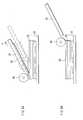
- FIGS. 7A and 7Bshow modification of the method of manufacturing the display unit according to the first embodiment.
- the touch panel 20is previously incurved by setting the face bonded to the adhesive layer 30 to outside, and pressed by the roller 80 from the other face.
- the display panel 10is formed. Subsequently, as shown in FIG. 7A , the touch panel 20 is previously incurved in the shape of, for example, approximate U, by setting the lower plastic film 21 bonded to the adhesive layer 30 to outside and by using a roll (not shown) and the like.
- the adhesive layer 30is formed on the display panel 10 , one end 20 A of the touch panel 20 which is previously incurved in the shape of U is placed on the display panel 10 , and the roller 80 is applied to the one end 20 A. Then, the roller 80 is applied to the touch-side plastic film 22 of the touch panel 20 .
- the touch panel 20 and the display panel 10are bonded together by pressing the touch panel 20 by the roller 80 from the touch-side plastic film 22 side by rolling and moving the roller 80 .
- forceis applied in the direction of tension to make the touch-side plastic film 22 flat. Therefore, in bonding and operation, no distortion or bending is generated in the touch-side plastic film 22 .
- the display unit shown in FIGS. 1 to 3is completed.
- FIG. 8shows a cross sectional structure of a display unit according to a second embodiment of the invention.
- This display unitis identical with the display unit described in the first embodiment except that the display panel 10 is not provided with the sealing panel 50 and the adhesive layer 60 , but is comprised of only the driving panel 40 . Therefore, the same components are applied with the same symbols, and their detailed explanations are omitted.
- the touch panel 20is bonded on the whole face on the side where the organic light emitting devices 10 R, 10 G, and 10 B of the driving substrate 11 are formed with the adhesive layer 30 in between.
- the light emitting devices 10 R, 10 G, and 10 Bare sealed by the touch panel 20 . Therefore, since the sealing panel 50 (refer to FIG. 1 ) and the adhesive layer 60 are omitted, thickness and weight of the display unit can be further reduced. Additionally, since the organic light emitting devices 10 R, 10 G, and 10 B are surely sealed by the protective film 11 A, the adhesive layer 30 , and the touch panel 20 , deterioration due to intrusion of moisture or oxygen can be prevented.
- a method of manufacturing the display unit in this embodimentis similar to that in the first embodiment except that the touch panel 20 and the display panel 10 are bonded together by forming the adhesive layer 30 on the protective film 11 A. Its function is similar to that in the first embodiment.
- the sealing panel 50is not provided, and the organic light emitting devices 10 R, 10 G, and 10 B are sealed by the touch panel 20 , thickness and weight of the display unit can be further reduced. Additionally, since the organic light emitting devices 10 R, 10 G, and 10 B are surely sealed by the protective film 11 A, the adhesive layer 30 , and the touch panel 20 , deterioration due to intrusion of moisture or oxygen can be prevented.
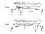
- the touch panel 20is attached to the touch panel holding plate 70 .
- the touch panel 20is attached to a mesh 92 which is stretched between frames 91 , and pressed by the roller 80 through the mesh 92 . This method is preferable since an angle of bend of the touch panel 20 is small so that a load to the touch panel 20 becomes small.
- the case using the touch panel 20 having the structure wherein the lower plastic film 21 and the touch-side plastic film 22 are layeredhas been described.
- the sealing panel 50is omitted as above, the conventional touch panel using a glass substrate instead of the lower plastic film 21 can be used in order to improve strength of the display unit.
- various driving methodscan be used, such as resistance film method, capacitance method, optical method, ultrasonic method, and electromagnetic induction method.
- the organic light emitting devices 10 R, 10 G, and 10 Btheir layer order can be opposite to that in the foregoing embodiments in such a way that the second electrode 14 , the organic layer 13 , and the first electrode 12 are layered on the driving substrate 11 in this order from the driving substrate 11 , and lights can be extracted from the driving substrate 11 side.
- the touch panel 20is placed on the driving substrate 11 on the side opposite to the organic light emitting devices 10 R, 10 G, and 10 B.
- the case using the first electrode 12 as an anode and the second electrode 14 as a cathodehas been described.
- anode and cathodeare reversed in such a way that the first electrode 12 is a cathode and the second electrode 14 is an anode.
- the second electrode 14 , the organic layer 13 , and the first electrode 12are layered on the driving substrate 11 in this order from the driving substrate 11 side, and the lights are extracted from the driving substrate 11 side.
- the structures of the organic light emitting deviceshave been specifically described. However, all layers are not necessarily provided, and other layer can be further provided.
- the first electrode 12has a two-layer structure wherein a transparent conductive film is layered on the top of a reflection film such as a dielectric multi-layer film or Al.
- a reflection filmsuch as a dielectric multi-layer film or Al.
- an end face of the reflection film on the light emitting layer sidecomposes an end of the resonation part
- the transparent conductive filmcomposes a part of the resonation part.
- the second electrode 14is comprised of the semi-transparent reflection layer.
- the second electrode 14has a structure wherein the semi-transparent reflection layer and a transparent electrode are layered from the first electrode 12 side.
- a function of this transparent electrodeis to lower electric resistance of the semi-transparent reflection layer.
- This transparent electrodeis made of a conductive material having a sufficient translucency to the lights generated in the light emitting layer.
- a material to make the transparent electrodefor example, ITO or a compound containing indium, zinc (Zn), and oxygen is preferable, since good conductivity can be obtained by using these materials even if deposition is made at room temperature.
- a thickness of the transparent electrodecan be, for example, 30 nm to 1,000 nm.
- the organic light emitting devices 10 R, 10 G, and 10 Bare formed on the driving substrate 11 .
- this inventioncan be applied to a display wherein other display devices such as an inorganic electroluminescence device is formed on the driving substrate 11 , FED (Field Emission Display), or a paper-like display which has been noted lately.
- the whole faces of the touch panel and the display panelare directly bonded together with the adhesive layer in between, a void between the touch panel and the display panel can be omitted and a thickness of the display unit can be reduced.
- the display panelsince the display panel has the sealing substrate which is placed opposite to the display device side of the substrate, and the whole faces of the substrate and the sealing substrate are bonded together with the adhesive layer in between, strength of the display panel is improved. Therefore, this display unit is extremely suitable as a display unit for mobile devices wherein a touch screen is essential and which require high strength.
- the touch panelhas a structure wherein two plastic films wherein respective transparent electrodes are formed are layered so that these transparent electrodes are placed opposite to each other, thickness and weight of the display unit is further reduced.
- the touch panelis such a touch panel with low rigidity, the touch panel is supported by the display panel.
- the touch panelis provided on the side where the display devices of the substrate are formed, and the display devices are sealed by the touch panel, thickness and weight of the display unit can be further reduced.
- the display devicesare surely sealed by the adhesive layer and the touch panel, deterioration can be prevented.
- the touch panel and the display panelare bonded together with the adhesive layer in between, one side of the touch panel is applied to the roller, and pressure force is applied by rotational movement of the roller, the touch panel and the display panel can be bonded together without mixing air bubbles into the adhesive layer. Therefore, deterioration of the display devices due to oxygen or moisture of air bubbles can be prevented, and image quality can be improved.
- the touch panelsince when the touch panel is pressed by the roller, the touch panel is previously incurved by setting the face bonded to the adhesive layer to outside, and the touch panel is pressed by the roller from the other face, i.e. the side to which contact by a finger or a pen is made, force is applied in the direction of tension to make the face to which contact by a finger or a pen is made flat. Therefore, in bonding, no distortion or bending is generated in the face to which contact by a finger or a pen is made, and image quality is improved.
Landscapes
- Engineering & Computer Science (AREA)
- Theoretical Computer Science (AREA)
- General Engineering & Computer Science (AREA)
- Computer Hardware Design (AREA)
- Human Computer Interaction (AREA)
- Physics & Mathematics (AREA)
- General Physics & Mathematics (AREA)
- Electroluminescent Light Sources (AREA)
Abstract
Description
- This application is a continuation of U.S. patent application Ser. No. 14/560,114 filed Dec. 4, 2014, which is a continuation of U.S. patent application Ser. No. 14/299,609 filed Jun. 9, 2014, which is a continuation of U.S. patent application Ser. No. 11/689,140, filed Mar. 21, 2007, now U.S. Pat. No. 8,808,477 issued on Aug. 19, 2014 which is a divisional of U.S. patent application Ser. No. 10/674,255, filed Sep. 29, 2003, which is now U.S. Pat. No. 7,936,338 issued on May 3, 2011, the entireties of all of which are incorporated herein by reference to the extent permitted by law. The present invention contains subject matter related to and claims priority to Japanese Patent Application No. 2002-288803 filed in the Japanese Patent Office on Oct. 1, 2002, the entirety of which also is incorporated by reference herein to the extent permitted by law.
- 1. Field of the Invention
- The present invention relates to a display unit having a touch panel and its manufacturing method, and more particularly such a display unit using organic light emitting devices and its manufacturing method.
- 2. Description of the Related Art
- A so-called touch screen, wherein a touch panel is mounted to a display panel using a CRT (Cathode Ray Tube) or a liquid crystal is widely used in banks, stations and the like. Additionally, a compact touch screen is adopted for a PDA (Personal Digital Assistant), a portable terminal and the like.
- A general touch panel used for conventional touch screens is, for example, has a structure wherein a glass substrate and a plastic film are layered. In such a touch panel, a glass substrate side is placed opposite to a display panel, so that a plastic film side becomes an operation face. In the case of a liquid crystal display panel, in order to prevent blooming phenomenon that images are distorted since the liquid crystal is transformed by getting pressure from touch panel operations, a void is provided between a glass substrate of the touch panel and the liquid crystal display panel.
- Lately, a touch panel having a structure wherein two plastic films are layered (hereinafter referred to as “flexible touch panel”) has been developed, and this flexible touch panel is expected as what allows the PDA, the portable terminal and the like to become further thinner and lighter. However, such a flexible touch panel has no rigidity itself since it has no glass substrate, so that the flexible touch panel should be supported by bonding a display panel thereto. Therefore, there is a problem that the flexible touch panel cannot be provided with a void between itself and the display panel as in a touch screen of a conventional liquid crystal display panel, so that it is difficult to mount the flexible touch panel to the liquid crystal display panel.
- To resolve the above problem, it is thinkable that a void is secured in the central part by fixing only four sides of the flexible touch panel on the display panel. In the case of taking such a measure for the conventional touch panel, when the plastic film is distorted or bent due to contact with a finger or a pen, distortion or bending can be restrained or recovered by the glass substrate. However, in the case of taking such a measure for the flexible touch panel, there is a problem that such distortion or bending cannot be restrained or recovered, and image quality may be lowered due to distortion or bending of the plastic film.
- Meanwhile, it is thinkable to construct a touch screen by bonding the flexible touch panel to an organic light emitting display, instead of the liquid crystal display. However, so far, there has been a problem that there is no established technique by which the flexible touch panel can be bonded to a whole face of the organic light emitting display without distortion or bending of the plastic film.
- Further, in a conventional organic light emitting display, a so-called can sealing structure is generally adopted. The can sealing structure is a structure wherein an adhesive is applied to the rim part of a rear panel, a sealing can made of metals or glass is bonded thereto, and a getter material such as calcium is enclosed in a space between the rear panel and the sealing can. In such an organic light emitting display having the can sealing structure, there is a problem that application to a touch screen of mobile devices particularly requiring high strength is difficult, since reducing thickness is limited and only four sides of the panel is fixed on the sealing can.
- In light of the foregoing, it is a first object of the invention to provide a display unit which can realize reduction of its thickness and weight by omitting a void between a touch panel and a display panel, and its manufacturing method.
- It is another object of the invention to provide a display unit which can improve image quality by preventing distortion or bending of the touch panel, and its manufacturing method.
- A display unit according to the invention comprises a display panel including a substrate wherein display devices are formed; and a touch panel which is directly bonded to the whole face of the display panel with an adhesive layer in between, and which detects contact with a finger or a pen.
- A method of manufacturing the display unit according to the invention includes the steps of forming the display panel including the substrate wherein the display devices are formed; and directly bonding a whole face of the touch panel which detects contact with a finger or a pen and the display panel together with the adhesive layer in between.
- In the display unit and its manufacturing method according to the invention, the whole faces of the touch panel and the display panel are directly bonded together with the adhesive layer in between. Therefore, there is no void between the touch panel and the display panel, so that a thickness of the display unit is reduced.
- Here, it is preferable that the display panel has a sealing substrate which is placed opposite to a display device side of the substrate, and the whole faces of the substrate and the sealing substrate are bonded together with the adhesive layer in between. By doing this, strength of the display panel becomes high, leading to obtaining a display unit suitable for mobile devices, wherein a touch screen is essential and which requires high strength.
- A suitable touch panel is, for example, a touch panel having a structure wherein two plastic films in which respective transparent electrodes are formed are layered so that the transparent electrodes are placed opposite to each other. The reason of it is that thickness and weight of the display unit is further reduced. Another reason of it is that even when the touch panel is such a touch panel with low rigidity, the touch panel is supported by the display panel, so that when distortion or bending is generated in the plastic film due to contact with a finger or a pen, such distortion or bending is restrained or recovered by the display panel.
- Further, a suitable display device is an organic light emitting device, which has an organic layer including a light emitting layer between a first electrode and a second electrode, and which extracts lights generated in the light emitting layer from the second electrode side. In the structure of the invention, the touch panel and the display panel are directly bonded without providing a void between the touch panel and the display panel since the organic light emitting device has no blooming phenomenon as in the liquid crystal. Therefore, by the structure of the invention, high image quality can be realized.
- Other and further objects, features and advantages of the invention will appear more fully from the following description.
FIG. 1 is a cross sectional view showing a construction of a display unit according to a first embodiment of the invention;FIG. 2 is an enlarged cross sectional view showing a construction of an organic layer in organic light emitting devices illustrated inFIG. 1 ;FIG. 3 is an enlarged cross sectional view showing a construction of an organic layer in an organic light emitting device illustrated inFIG. 1 ;FIGS. 4A and 4B are cross sectional views showing a method of manufacturing the display unit illustrated inFIG. 1 in the order of processes;FIG. 5 is a cross sectional view showing a process followingFIGS. 4A and 4B ;FIGS. 6A and 6B are explanation drawings showing a process followingFIG. 5 ;FIGS. 7A to 7C are explanation drawings showing a method of manufacturing a display unit according to a modification of the invention;FIG. 8 is a cross sectional view showing a construction of a display unit according to a second embodiment of the invention; andFIGS. 9A and 9B are explanation drawings showing a method of manufacturing the display unit according to the modification of the invention.- Embodiments of the invention will be described in detail hereinbelow with reference to the drawings.
FIG. 1 shows a cross sectional structure of a display unit according to a first embodiment of the invention. This display unit is used as an ultrathin organic light emitting color display unit or the like, and, for example, atouch panel 20 is bonded to a whole face of adisplay panel 10 by anadhesive layer 30.- In the
display panel 10, for example, a drivingpanel 40 and a sealingpanel 50 are placed opposite, and whole faces of both thepanels adhesive layer 60. - The driving
panel 40 has a structure wherein, for example, an organiclight emitting device 10R which emits red lights, an organiclight emitting device 10G which emits green lights, and an organiclight emitting device 10B which emits blue lights are provided in order in a matrix state as a whole, on a drivingsubstrate 11 made of an insulating material such as glass. In addition, the drivingsubstrate 11 is provided with a protective film (passivation film)11A to prevent moisture and the like from intruding into the organiclight emitting devices - In the organic
light emitting devices first electrode 12 as an anode, anorganic layer 13, and asecond electrode 14 as a cathode are layered in this order from the drivingsubstrate 11 side. On thesecond electrode 14, theprotective film 11A is formed. - The
first electrode 12 also has a function as a reflection layer, and it is desirable that thefirst electrode 12 has a reflectance as high as possible in order to improve light emitting efficiency. For example, materials to make thefirst electrode 12 include simple substances or alloys of metal elements with high work function, such as platinum (Pt), gold (Au), silver (Ag), chromium (Cr), tungsten (W) and the like. A thickness of thefirst electrode 12 in the layer direction (hereinafter simply referred to as “thickness”) is preferably from 100 nm to 300 nm. As an alloy material, for example, AgPdCu alloy, whose main component is silver, and which contains palladium (Pd) of 0.3 wt % to 1 wt % and copper (Cu) of 0.3 wt % to 1 wt % can be cited. - A construction of the
organic layer 13 varies according to light emitting colors of the organiclight emitting device 10.FIG. 2 shows an enlarged view of a construction of theorganic layer 13 in the organiclight emitting devices organic layer 13 of the organiclight emitting devices hole injection layer 13A, an electronhole transport layer 13B, a light emitting layer13C, an electron transport layer13D, and anelectron injection layer 13E are layered in this order from thefirst electrode 12 side. A function of the electronhole injection layer 13A and the electronhole transport layer 13B is to improve efficiency to inject electron holes into the light emitting layer13C. A function of the light emitting layer13C is to produce lights by current injection. A function of the electron transport layer13D and theelectron injection layer 13E is to improve efficiency to inject electrons into the light emitting layer13C. - The electron
hole injection layer 13A of the organiclight emitting device 10R, for example, has a thickness of about 30 nm, and made of 4,4′,4″-tris(3-methylphenyl phenyl amino)tri-phenyl amine (MTDATA). The electronhole transport layer 13B of the organiclight emitting device 10R, for example, has a thickness of about 30 nm, and made of bis [(N-naphthyl)-N-phenyl]benzidine (α-NPD). The light emitting layer13C of the organiclight emitting device 10R, for example, has a thickness of about 50 nm, and made of 2,5-bis [4-[N-(4-methoxyphenyl)-N-phenylamino]]stilbenzene-1,4-dica-bonitrile (BSB). The electron transport layer13D of the organiclight emitting device 10R, for example, has a thickness of about 30 nm, and made of 8-quinolinol aluminum complex (Alq). Theelectron injection layer 13E of the organiclight emitting device 10R, for example, has a thickness of 1 nm, and made of lithium fluoride (LiF). - The electron
hole injection layer 13A of the organiclight emitting device 10B, for example, has a thickness of about 30 nm, and made of MTDATA. The electronhole transport layer 13B of the organiclight emitting device 10B, for example, has a thickness of about 30 nm, and made of α-NPD. The light emitting layer13C of the organiclight emitting device 10B, for example, has a thickness of about 30 nm, and made of spiro6 Φ. The electron transport layer13D of the organiclight emitting device 10B, for example, has a thickness of about 30 nm, and made of Alq. Theelectron injection layer 13E of the organiclight emitting device 10B, for example, has a thickness of about 1 nm, and made of lithium fluoride (LiF). FIG. 3 shows an enlarged view of a construction of theorganic layer 13 in the organiclight emitting device 10G. Theorganic layer 13 of the organiclight emitting device 10G has a structure wherein the electronhole injection layer 13A, the electronhole transport layer 13B, the light emitting layer13C, and theelectron injection layer 13E are layered in this order from thefirst electrode 12 side. The light emitting layer13C also has a function as an electron transport layer.- The electron
hole injection layer 13A of the organiclight emitting device 10G, for example, has a thickness of about 30 nm, and made of MTDATA. The electronhole transport layer 13B of the organiclight emitting device 10G, for example, has a thickness of about 30 nm, and made of α-NPD. The light emitting layer13C of the organiclight emitting device 10G, for example, has a thickness of about 60 nm, and made of Alq. Theelectron injection layer 13E of the organiclight emitting device 10G, for example, has a thickness of about 1 nm, and made of lithium fluoride (LiF). - The
second electrode 14 shown inFIGS. 1 to 3 , for example, has a thickness of 1 nm to 50 nm, and made of a simple substance or an alloy of metal elements with low work function, such as aluminum (Al), magnesium (Mg), calcium (Ca), sodium (Na) and the like. Specially, an alloy made of magnesium and silver (MgAg alloy) is preferable, and a mass ratio of magnesium and silver is preferably Mg:Ag=5:1 to 20:1. - The
second electrode 14 also has a function as a semi-transparent reflection layer. Namely, these organiclight emitting devices first electrode 12 on the light emitting layer13C side as a first end P1, an end face of thesecond electrode 14 on the light emitting layer13C side as the second end P2, and theorganic layer 13 as a resonance part. Such a resonator structure is preferable, since the lights generated in the light emitting layer13C generate multiple interference, and act as a kind of narrow band filter, so that half bandwidth of spectrum of the extracted light is reduced, and color purity can be improved. Further, such a resonator structure is preferable, since outside lights entering from the sealingpanel 50 can be attenuated by the multiple interference as well, and reflectance of outside lights in the organiclight emitting devices color filter 52 described later (refer toFIG. 1 ). - To obtain the above effects, it is preferable that an optical distance L between the first end P1 and the second end P2 of the resonator satisfies
Mathematical Expression 1, and a resonance wave length of the resonator (peak wave length of the spectrum of the extracted light) corresponds to a peak wave length of spectrum of the light to be extracted. Actually, it is preferable that the optical distance L is selected so that L becomes a positive minimum value which satisfies theMathematical Expression 1.
(2L)/λ+Φ/(2π)=m [Mathematical Expression 1]- (In the mathematical expression, L represents an optical distance between the first end P1 and the second end P2, Φ represents a phase shift (rad) of the reflection light generated in the first end P1 and the second end P2, λ represents a peak wave length of spectrum of the light to be extracted from the second end P2 side, and m represents a whole number which makes L be a positive number. In the
Mathematical Expression 1, L and λ should share a common unit such as (nm).) - The sealing
panel 50 shown inFIG. 1 has a sealingsubstrate 51 which seals the organiclight emitting devices adhesive layer 60. The sealingsubstrate 51 is made of a material such as glass which is transparent to the lights generated in the organiclight emitting devices substrate 51 is, for example, provided with thecolor filter 52, extracts the lights generated in the organiclight emitting devices light emitting devices - The
color filter 52 can be arranged on either face of the sealingsubstrate 51. However, it is preferable to arrange thecolor filter 52 on the drivingpanel 40 side. The reason of it is that thecolor filter 52 is not exposed on the surface and a structure wherein antiweatherability of thecolor filter 52 is considered can be obtained. Another reason of it is that when bonding thedisplay panel 10 and thetouch panel 20, problems such as unevenness in thetouch panel 20 can be prevented. Thecolor filter 52 has ared color filter 52R, agreen filter 52G, and ablue filter 52B, which are positioned corresponding to the organiclight emitting devices - The
red color filter 52R, thegreen filter 52G, and theblue filter 52B are, for example, respectively formed in the shape of rectangle with no space between them. Thered color filter 52R, thegreen filter 52G, and theblue filter 52B are respectively made of a resin mixed with pigments, and adjusted so that light transmission in the targeted wave length band of red, green or blue becomes high and light transmission in other wave length band becomes low by selecting a pigment. - Further, a wave length range with high light transmittance in the
color filter 52 corresponds to a peak wave length2, of spectrum of the light extracted from the resonator structure. Therefore, out of outside lights entering from the sealingpanel 50, only the light having a wave length equal to the peak wave length of spectrum of the light to be extracted filters out through thecolor filter 52, and other outside lights having other wave lengths are prevented from intruding into the organiclight emitting devices - The
protective film 11A shown inFIG. 1 is made of, for example, silicon oxide (SiO2), silicon nitride (SiNx) and the like. A function of theprotective film 11A is to prevent oxygen, moisture and the like from intruding into the organiclight emitting devices - The
touch panel 20 shown inFIG. 1 is a flexible touch panel which has a structure, for example, wherein alower plastic film 21 and a touch-side plastic film 22 are layered with an unshown spacer in between, and located on the sealingsubstrate 51 on the side opposite to the drivingsubstrate 11. In order to detect contact to the touch-side plastic film 22 by a finger, a pen or the like, in thistouch panel 20, for example, thelower plastic film 21 is provided with atransparent electrode 21A, and the touch-side plastic film 22 is provided with atransparent electrode 22A. Thelower plastic film 21 and the touch-side plastic film 22 are layered so that thetransparent electrodes transparent electrodes - This display unit can be, for example, produced as follows.
FIGS. 4A and 4B to 6A and 6B show a method of manufacturing this display unit in the order of processes. First, as shown inFIG. 4A , on the drivingsubstrate 11 made of the above-mentioned material, thefirst electrode 12 made of the above-mentioned material is deposited in the foregoing thickness by, for example, DC sputtering, selective etching is made by using, for example, lithography technique, and patterning is made in the form of a given shape. After that, as shown inFIG. 4A , the electronhole injection layer 13A, the electronhole transport layer 13B, the light emitting layer13C, the electron transport layer13D, theelectron injection layer 13E, and thesecond electrode 14 which have the foregoing thicknesses and are made of the foregoing materials, are sequentially deposited, for example, by deposition method, and the organiclight emitting devices FIGS. 2 and 3 are formed. After that, as shown inFIG. 4A as well, theprotective film 11A made of the above-mentioned material is formed to cover the organiclight emitting devices substrate 11. Consequently, the drivingpanel 40 is formed.- As shown in
FIG. 4B , thered filter 52R is formed by, for example, on the sealingsubstrate 51 made of the foregoing material, a material for thered filter 52R is applied by spin coat method, and burning is made with patterning by photolithography. Subsequently, as shown inFIG. 4B as well, theblue filter 52B and thegreen filter 52G are sequentially formed in the same manner as in thered filter 52R. Consequently, the sealingpanel 50 is formed. - Subsequently, as shown in
FIG. 5 , theadhesive layer 60 is formed on theprotective film 11A, the sealingsubstrate 51 wherein thecolor film 52 is formed is placed opposite to the side of the organiclight emitting devices substrate 11, and whole faces of the sealingsubstrate 51 and the drivingsubstrate 11 are bonded with theadhesive layer 60 in between. Then, it is preferable that a side of the sealingpanel 50 where thecolor filter 52 is formed is placed opposite to the drivingpanel 40. Consequently, thedisplay panel 10 is formed. - After that, as shown in
FIGS. 6A and 6B , theadhesive layer 30 is formed on thedisplay panel 10, and the whole faces of thetouch panel 20 and thedisplay panel 10 are bonded with theadhesive layer 30 in between. Then, first, as shown inFIG. 6A , thetouch panel 20 is attached to a touchpanel holding plate 70, and aroller 80 is applied onto one side of thetouch panel 20. Subsequently, as shown inFIG. 6B , thetouch panel 20 and thedisplay panel 10 are bonded by pressure force generated by rotational movement of theroller 80. Then, thetouch panel 20 is slid on the touchpanel holding plate 70 by moving the touchpanel holding plate 70 in the direction of arrow A in sync with theroller 80. Consequently, thetouch panel 20 and thedisplay panel 10 can be bonded together without mixing air bubbles into theadhesive layer 30. As above, the display unit shown inFIGS. 1 to 3 is completed. - In this display unit, when a given voltage is applied between the
first electrode 12 and thesecond electrode 14, current is injected into the light emitting layer13C, and an electron hole and an electron recombines, leading to light emitting mainly at the interface of the light emitting layer13C. This light multiple-reflects between thefirst electrode 12 and thesecond electrode 14, and extracted through thesecond electrode 14, theprotective film 11A, thecolor filter 52, the sealingsubstrate 51, and thetouch panel 20. When a finger or a pen contacts the touch-side plastic film 22, thetouch panel 20 detects the contact. Then, in this embodiment, since the whole faces of thetouch panel 20 and thedisplay panel 10 are directly bonded together with theadhesive layer 30 in between so that thetouch panel 20 is supported by thedisplay panel 10, even when a finger or a pen contacts thetouch panel 20, no distortion or bending is generated in thetouch panel 20, and image quality is improved. - As above, according to this embodiment, since the whole faces of the
touch panel 20 and thedisplay panel 10 are directly bonded with theadhesive layer 30 in between, a void between thetouch panel 20 and thedisplay panel 10 is omitted, and a thickness of the display unit can be reduced. - In particular, since the
display panel 10 has a structure wherein the whole faces of the drivingsubstrate 11 and the sealingsubstrate 51 are bonded together with theadhesive layer 60 in between, strength of thedisplay panel 10 is raised. Therefore, this display unit is very suitable as a display unit for mobile devices wherein a touch screen is essential and which require high strength. - Further, the
touch panel 20 is a flexible touch panel having the structure, wherein thelower plastic film 21 formed with thetransparent electrode 21A and the touch-side plastic film 22 formed with thetransparent electrode 22A are layered so that thetransparent electrodes touch panel 20 is such a touch panel with low rigidity, since thetouch panel 20 is supported by thedisplay panel 10, when distortion or bending is generated in the touch-side plastic film 22 and the like due to contact with a finger or a pen, such distortion or bending can be restrained or recovered by thedisplay panel 10. - In addition, particularly, since when the
touch panel 20 and thedisplay panel 10 are bonded together with theadhesive layer 30 in between, theroller 80 is applied onto one side of thetouch panel 20 and pressure force is applied by rotating and moving theroller 80, thetouch panel 20 and thedisplay panel 10 can be bonded without mixing air bubbles into theadhesive layer 30. Consequently, deterioration of the organiclight emitting devices FIGS. 7A and 7B show modification of the method of manufacturing the display unit according to the first embodiment. In this modification, thetouch panel 20 is previously incurved by setting the face bonded to theadhesive layer 30 to outside, and pressed by theroller 80 from the other face.- First, in the same manner as in what shown in
FIGS. 4A, 4B and 5 in the first embodiment, thedisplay panel 10 is formed. Subsequently, as shown inFIG. 7A , thetouch panel 20 is previously incurved in the shape of, for example, approximate U, by setting thelower plastic film 21 bonded to theadhesive layer 30 to outside and by using a roll (not shown) and the like. - Next, as shown in
FIG. 7B , theadhesive layer 30 is formed on thedisplay panel 10, one end20A of thetouch panel 20 which is previously incurved in the shape of U is placed on thedisplay panel 10, and theroller 80 is applied to the one end20A. Then, theroller 80 is applied to the touch-side plastic film 22 of thetouch panel 20. - Subsequently, as shown in
FIG. 7C , thetouch panel 20 and thedisplay panel 10 are bonded together by pressing thetouch panel 20 by theroller 80 from the touch-side plastic film 22 side by rolling and moving theroller 80. In this way, force is applied in the direction of tension to make the touch-side plastic film 22 flat. Therefore, in bonding and operation, no distortion or bending is generated in the touch-side plastic film 22. As above, the display unit shown inFIGS. 1 to 3 is completed. - As above, in this modification, since the
touch panel 20 is previously incurved by setting thelower plastic film 21 bonded to theadhesive layer 30 to outside, and thetouch panel 20 and thedisplay panel 10 are bonded by pressing thetouch panel 20 by theroller 80 from the touch-side plastic film 22 side, force is applied in the direction of tension to make the touch-side plastic film 22 of thetouch panel 20 flat. Therefore, in bonding and operation, no distortion or bending is generated in the touch-side plastic film 22, and image quality is improved. FIG. 8 shows a cross sectional structure of a display unit according to a second embodiment of the invention. This display unit is identical with the display unit described in the first embodiment except that thedisplay panel 10 is not provided with the sealingpanel 50 and theadhesive layer 60, but is comprised of only the drivingpanel 40. Therefore, the same components are applied with the same symbols, and their detailed explanations are omitted.- The
touch panel 20 is bonded on the whole face on the side where the organiclight emitting devices substrate 11 are formed with theadhesive layer 30 in between. Thelight emitting devices touch panel 20. Therefore, since the sealing panel50 (refer toFIG. 1 ) and theadhesive layer 60 are omitted, thickness and weight of the display unit can be further reduced. Additionally, since the organiclight emitting devices protective film 11A, theadhesive layer 30, and thetouch panel 20, deterioration due to intrusion of moisture or oxygen can be prevented. - A method of manufacturing the display unit in this embodiment is similar to that in the first embodiment except that the
touch panel 20 and thedisplay panel 10 are bonded together by forming theadhesive layer 30 on theprotective film 11A. Its function is similar to that in the first embodiment. - As above, in this embodiment, since the sealing
panel 50 is not provided, and the organiclight emitting devices touch panel 20, thickness and weight of the display unit can be further reduced. Additionally, since the organiclight emitting devices protective film 11A, theadhesive layer 30, and thetouch panel 20, deterioration due to intrusion of moisture or oxygen can be prevented. - While the invention has been described with reference to the embodiments, the invention is not limited to the foregoing embodiments, and various modifications may be made. For example, materials, thickness, deposition methods, and deposition conditions for respective layers are not limited to those described in the foregoing embodiments, and other materials, thickness, deposition methods, and deposition conditions can be applied.
- For example, in the foregoing first embodiment, the
touch panel 20 is attached to the touchpanel holding plate 70. However, it is possible that, as shown inFIGS. 9A and 9B , instead of the touchpanel holding plate 70, thetouch panel 20 is attached to amesh 92 which is stretched betweenframes 91, and pressed by theroller 80 through themesh 92. This method is preferable since an angle of bend of thetouch panel 20 is small so that a load to thetouch panel 20 becomes small. - Further, in the foregoing second embodiment, the case using the
touch panel 20 having the structure wherein thelower plastic film 21 and the touch-side plastic film 22 are layered has been described. However, in the case where the sealingpanel 50 is omitted as above, the conventional touch panel using a glass substrate instead of thelower plastic film 21 can be used in order to improve strength of the display unit. - Further, the foregoing modification can be applied not only to the first embodiment, but also to the second embodiment. It is hereby possible to realize a more thinner and lighter display unit.
- Further, for example, for the
touch panel 20, various driving methods can be used, such as resistance film method, capacitance method, optical method, ultrasonic method, and electromagnetic induction method. - Further, for example, regarding a structure of the organic
light emitting devices second electrode 14, theorganic layer 13, and thefirst electrode 12 are layered on the drivingsubstrate 11 in this order from the drivingsubstrate 11, and lights can be extracted from the drivingsubstrate 11 side. In this case, thetouch panel 20 is placed on the drivingsubstrate 11 on the side opposite to the organiclight emitting devices - Further, for example, in the foregoing embodiments, the case using the
first electrode 12 as an anode and thesecond electrode 14 as a cathode has been described. However, it is possible that anode and cathode are reversed in such a way that thefirst electrode 12 is a cathode and thesecond electrode 14 is an anode. Further, it is possible, along with using thefirst electrode 12 as a cathode and thesecond electrode 14 as an anode, thesecond electrode 14, theorganic layer 13, and thefirst electrode 12 are layered on the drivingsubstrate 11 in this order from the drivingsubstrate 11 side, and the lights are extracted from the drivingsubstrate 11 side. - Further, in the foregoing embodiments, the structures of the organic light emitting devices have been specifically described. However, all layers are not necessarily provided, and other layer can be further provided. For example, it is possible that the
first electrode 12 has a two-layer structure wherein a transparent conductive film is layered on the top of a reflection film such as a dielectric multi-layer film or Al. In this case, an end face of the reflection film on the light emitting layer side composes an end of the resonation part, and the transparent conductive film composes a part of the resonation part. - Further, in the foregoing embodiments, the case wherein the
second electrode 14 is comprised of the semi-transparent reflection layer has been described. However, it is possible that thesecond electrode 14 has a structure wherein the semi-transparent reflection layer and a transparent electrode are layered from thefirst electrode 12 side. A function of this transparent electrode is to lower electric resistance of the semi-transparent reflection layer. This transparent electrode is made of a conductive material having a sufficient translucency to the lights generated in the light emitting layer. As a material to make the transparent electrode, for example, ITO or a compound containing indium, zinc (Zn), and oxygen is preferable, since good conductivity can be obtained by using these materials even if deposition is made at room temperature. A thickness of the transparent electrode can be, for example, 30 nm to 1,000 nm. - Further, in the foregoing embodiments, the case wherein the organic
light emitting devices substrate 11 has been described. However, this invention can be applied to a display wherein other display devices such as an inorganic electroluminescence device is formed on the drivingsubstrate 11, FED (Field Emission Display), or a paper-like display which has been noted lately. - As described above, according to the display unit of the invention or the method of manufacturing the display unit of the invention, since the whole faces of the touch panel and the display panel are directly bonded together with the adhesive layer in between, a void between the touch panel and the display panel can be omitted and a thickness of the display unit can be reduced.
- According to the display unit of one aspect of the invention or the method of manufacturing the display unit of one aspect of the invention, since the display panel has the sealing substrate which is placed opposite to the display device side of the substrate, and the whole faces of the substrate and the sealing substrate are bonded together with the adhesive layer in between, strength of the display panel is improved. Therefore, this display unit is extremely suitable as a display unit for mobile devices wherein a touch screen is essential and which require high strength.
- According to the display unit of another aspect of the invention or the method of manufacturing the display unit of another aspect of the invention, since the touch panel has a structure wherein two plastic films wherein respective transparent electrodes are formed are layered so that these transparent electrodes are placed opposite to each other, thickness and weight of the display unit is further reduced. In addition, even if the touch panel is such a touch panel with low rigidity, the touch panel is supported by the display panel. Thus, when distortion or bending is generated in the plastic film due to contact with a finger or a pen, such distortion or bending is restrained or recovered by the display panel.
- According to the display unit of still another aspect of the invention or the method of manufacturing the display unit of still another aspect of the invention, since the touch panel is provided on the side where the display devices of the substrate are formed, and the display devices are sealed by the touch panel, thickness and weight of the display unit can be further reduced. In addition, since the display devices are surely sealed by the adhesive layer and the touch panel, deterioration can be prevented.
- According to the method of manufacturing the display unit of still another aspect of the invention, since when the touch panel and the display panel are bonded together with the adhesive layer in between, one side of the touch panel is applied to the roller, and pressure force is applied by rotational movement of the roller, the touch panel and the display panel can be bonded together without mixing air bubbles into the adhesive layer. Therefore, deterioration of the display devices due to oxygen or moisture of air bubbles can be prevented, and image quality can be improved.
- According to the method of manufacturing the display unit of still another aspect of the invention, since when the touch panel is pressed by the roller, the touch panel is previously incurved by setting the face bonded to the adhesive layer to outside, and the touch panel is pressed by the roller from the other face, i.e. the side to which contact by a finger or a pen is made, force is applied in the direction of tension to make the face to which contact by a finger or a pen is made flat. Therefore, in bonding, no distortion or bending is generated in the face to which contact by a finger or a pen is made, and image quality is improved.
- Obviously many modifications and variations of the present invention are possible in the light of the above teachings. It is therefore to be understood that within the scope of the appended claims the invention may be practiced otherwise than as specifically described.
Claims (20)
Priority Applications (3)
| Application Number | Priority Date | Filing Date | Title |
|---|---|---|---|
| US15/612,718US10571965B2 (en) | 2002-10-01 | 2017-06-02 | Display unit and its manufacturing method |
| US16/744,501US10817019B2 (en) | 2002-10-01 | 2020-01-16 | Display unit and its manufacturing method |
| US17/020,817US11586244B2 (en) | 2002-10-01 | 2020-09-15 | Display unit and its manufacturing method |
Applications Claiming Priority (7)
| Application Number | Priority Date | Filing Date | Title |
|---|---|---|---|
| JP2002288803 | 2002-10-01 | ||
| JP2002-288803 | 2002-10-01 | ||
| US10/674,255US7936338B2 (en) | 2002-10-01 | 2003-09-29 | Display unit and its manufacturing method |
| US11/689,140US8808477B2 (en) | 2002-10-01 | 2007-03-21 | Display unit and its manufacturing method |
| US14/299,609US20140285738A1 (en) | 2002-10-01 | 2014-06-09 | Display unit and its manufacturing method |
| US14/560,114US9720448B2 (en) | 2002-10-01 | 2014-12-04 | Display unit and its manufacturing method |
| US15/612,718US10571965B2 (en) | 2002-10-01 | 2017-06-02 | Display unit and its manufacturing method |
Related Parent Applications (1)
| Application Number | Title | Priority Date | Filing Date |
|---|---|---|---|
| US14/560,114ContinuationUS9720448B2 (en) | 2002-10-01 | 2014-12-04 | Display unit and its manufacturing method |
Related Child Applications (1)
| Application Number | Title | Priority Date | Filing Date |
|---|---|---|---|
| US16/744,501ContinuationUS10817019B2 (en) | 2002-10-01 | 2020-01-16 | Display unit and its manufacturing method |
Publications (2)
| Publication Number | Publication Date |
|---|---|
| US20170269635A1true US20170269635A1 (en) | 2017-09-21 |
| US10571965B2 US10571965B2 (en) | 2020-02-25 |
Family
ID=32652535
Family Applications (7)
| Application Number | Title | Priority Date | Filing Date |
|---|---|---|---|
| US10/674,255Expired - LifetimeUS7936338B2 (en) | 2002-10-01 | 2003-09-29 | Display unit and its manufacturing method |
| US11/689,140Active2026-02-23US8808477B2 (en) | 2002-10-01 | 2007-03-21 | Display unit and its manufacturing method |
| US14/299,609AbandonedUS20140285738A1 (en) | 2002-10-01 | 2014-06-09 | Display unit and its manufacturing method |
| US14/560,114Expired - Fee RelatedUS9720448B2 (en) | 2002-10-01 | 2014-12-04 | Display unit and its manufacturing method |
| US15/612,718Expired - LifetimeUS10571965B2 (en) | 2002-10-01 | 2017-06-02 | Display unit and its manufacturing method |
| US16/744,501Expired - Fee RelatedUS10817019B2 (en) | 2002-10-01 | 2020-01-16 | Display unit and its manufacturing method |
| US17/020,817Expired - LifetimeUS11586244B2 (en) | 2002-10-01 | 2020-09-15 | Display unit and its manufacturing method |
Family Applications Before (4)
| Application Number | Title | Priority Date | Filing Date |
|---|---|---|---|
| US10/674,255Expired - LifetimeUS7936338B2 (en) | 2002-10-01 | 2003-09-29 | Display unit and its manufacturing method |
| US11/689,140Active2026-02-23US8808477B2 (en) | 2002-10-01 | 2007-03-21 | Display unit and its manufacturing method |
| US14/299,609AbandonedUS20140285738A1 (en) | 2002-10-01 | 2014-06-09 | Display unit and its manufacturing method |
| US14/560,114Expired - Fee RelatedUS9720448B2 (en) | 2002-10-01 | 2014-12-04 | Display unit and its manufacturing method |
Family Applications After (2)
| Application Number | Title | Priority Date | Filing Date |
|---|---|---|---|
| US16/744,501Expired - Fee RelatedUS10817019B2 (en) | 2002-10-01 | 2020-01-16 | Display unit and its manufacturing method |
| US17/020,817Expired - LifetimeUS11586244B2 (en) | 2002-10-01 | 2020-09-15 | Display unit and its manufacturing method |
Country Status (5)
| Country | Link |
|---|---|
| US (7) | US7936338B2 (en) |
| KR (1) | KR100971053B1 (en) |
| CN (1) | CN100350360C (en) |
| SG (1) | SG121800A1 (en) |
| TW (1) | TWI284003B (en) |
Cited By (3)
| Publication number | Priority date | Publication date | Assignee | Title |
|---|---|---|---|---|
| CN110481045A (en)* | 2019-09-16 | 2019-11-22 | 江苏铁锚玻璃股份有限公司 | The bonding structure and preparation method thereof of the transparence display touch screen of loss of weight |
| US10678304B2 (en) | 2014-02-12 | 2020-06-09 | Samsung Display Co., Ltd. | Display device and method of manufacturing a display device |
| US20210313549A1 (en)* | 2019-07-02 | 2021-10-07 | Boe Technology Group Co., Ltd. | Display panel and method for manufacturing the same, and display device |
Families Citing this family (56)
| Publication number | Priority date | Publication date | Assignee | Title |
|---|---|---|---|---|
| US7936338B2 (en) | 2002-10-01 | 2011-05-03 | Sony Corporation | Display unit and its manufacturing method |
| TWI272037B (en)* | 2005-03-31 | 2007-01-21 | Au Optronics Corp | Organic electroluminescent display panel |
| JP4743038B2 (en)* | 2005-08-22 | 2011-08-10 | セイコーエプソン株式会社 | Electroluminescence device and manufacturing method thereof |
| TWI313431B (en)* | 2006-04-14 | 2009-08-11 | Ritdisplay Corporatio | Transparent touch panel |
| JP4910780B2 (en)* | 2007-03-02 | 2012-04-04 | セイコーエプソン株式会社 | Organic electroluminescence device with input function and electronic device |
| JP5103944B2 (en)* | 2007-03-02 | 2012-12-19 | セイコーエプソン株式会社 | Organic electroluminescence device with input function and electronic device |
| KR100873080B1 (en)* | 2007-05-10 | 2008-12-09 | 삼성모바일디스플레이주식회사 | Organic electroluminescent display |
| KR20090112118A (en)* | 2008-04-23 | 2009-10-28 | 엘지이노텍 주식회사 | Display |
| TWI400509B (en)* | 2008-06-13 | 2013-07-01 | Prime View Int Co Ltd | Flexible display module and method of manufacturing the same |
| US8928597B2 (en) | 2008-07-11 | 2015-01-06 | Samsung Display Co., Ltd. | Organic light emitting display device |
| US8629842B2 (en)* | 2008-07-11 | 2014-01-14 | Samsung Display Co., Ltd. | Organic light emitting display device |
| US9342176B2 (en) | 2008-07-21 | 2016-05-17 | Samsung Display Co., Ltd. | Organic light emitting display device |
| JP2010032938A (en) | 2008-07-31 | 2010-02-12 | Hitachi Displays Ltd | Liquid crystal display |
| KR20100024710A (en)* | 2008-08-26 | 2010-03-08 | 삼성모바일디스플레이주식회사 | Organic light emitting diode display |
| JP2011003522A (en) | 2008-10-16 | 2011-01-06 | Semiconductor Energy Lab Co Ltd | Flexible light-emitting device, electronic equipment, and method of manufacturing flexible light-emitting device |
| JP2010153813A (en) | 2008-11-18 | 2010-07-08 | Semiconductor Energy Lab Co Ltd | Light-emitting device, method of manufacturing the same, and portable telephone |
| KR101634791B1 (en) | 2008-11-28 | 2016-06-30 | 삼성디스플레이 주식회사 | Touch sensible organic light emitting diode display |
| KR101048980B1 (en) | 2009-01-16 | 2011-07-12 | 삼성모바일디스플레이주식회사 | Touch screen panel and its manufacturing method |
| CN101848610A (en)* | 2009-03-27 | 2010-09-29 | 深圳富泰宏精密工业有限公司 | Shell and manufacturing method thereof |
| TWI391886B (en)* | 2009-06-12 | 2013-04-01 | Au Optronics Corp | Flexible touch display apparatus |
| US8576209B2 (en) | 2009-07-07 | 2013-11-05 | Semiconductor Energy Laboratory Co., Ltd. | Display device |
| KR20110037337A (en)* | 2009-10-06 | 2011-04-13 | 엘지디스플레이 주식회사 | Organic light emitting display device and manufacturing method thereof |
| KR101695019B1 (en)* | 2009-12-18 | 2017-01-11 | 엘지디스플레이 주식회사 | Organic Light Emitting Device and Method For The Same |
| KR101107173B1 (en)* | 2010-02-11 | 2012-01-25 | 삼성모바일디스플레이주식회사 | Organic light emitting display device and manufacturing method thereof |
| KR101756656B1 (en)* | 2010-06-25 | 2017-07-11 | 엘지디스플레이 주식회사 | Organic light emitting diode display device including touch panel |
| JP5485834B2 (en)* | 2010-09-01 | 2014-05-07 | スリーエム イノベイティブ プロパティズ カンパニー | Image display device manufacturing method and image display device manufacturing apparatus |
| JP5652100B2 (en)* | 2010-10-05 | 2015-01-14 | ソニー株式会社 | Display panel, display device, lighting panel and lighting device, and display panel and lighting panel manufacturing method |
| KR101320384B1 (en) | 2011-06-30 | 2013-10-23 | 삼성디스플레이 주식회사 | Flexible display panel and the display apparatus comprising the flexible display panel |
| KR101919107B1 (en) | 2012-05-08 | 2018-11-16 | 삼성디스플레이 주식회사 | Display device |
| GB2502600B8 (en) | 2012-05-31 | 2015-01-07 | Improvements in touch sensitive displays | |
| GB2502602B (en)* | 2012-05-31 | 2015-06-03 | Zytronic Displays Ltd | Multi-touch sensing panel production method |
| KR101382601B1 (en)* | 2012-07-02 | 2014-04-17 | 삼성디스플레이 주식회사 | Manufacturing apparatus and method of organic light emitting diode display |
| US20140009429A1 (en)* | 2012-07-03 | 2014-01-09 | Chimei Innolux Corporation | Method of producing capacitive coplanar touch panel devices with laser ablation |
| KR102173801B1 (en) | 2012-07-12 | 2020-11-04 | 가부시키가이샤 한도오따이 에네루기 켄큐쇼 | Display device and method for manufacturing display device |
| US20140062916A1 (en)* | 2012-08-28 | 2014-03-06 | Lg Display Co., Ltd. | Touch panel and method of manufacturing the same and display device using the same |
| KR101930383B1 (en)* | 2012-10-31 | 2019-03-11 | 엘지디스플레이 주식회사 | Organic Light Emitting Device and Method of manufacturing the same |
| KR101453880B1 (en) | 2012-11-29 | 2014-10-22 | 삼성디스플레이 주식회사 | Organic light emitting display apparatus and the method for manufacturing the same |
| GB2511780B (en)* | 2013-03-12 | 2017-04-19 | Tcs John Huxley Europe Ltd | Gaming table |
| TWI497386B (en)* | 2013-03-22 | 2015-08-21 | Innolux Corp | Display apparatus with touch sensor and method for manufacturing the same |
| KR20140123735A (en)* | 2013-04-15 | 2014-10-23 | 삼성디스플레이 주식회사 | Adhesive having adhesive capsule and organic light emitting display device comprising adhesive layer formed by the adhesive |
| KR102150711B1 (en)* | 2013-05-28 | 2020-09-02 | 삼성디스플레이 주식회사 | Flexible display apparatus |
| JP6253923B2 (en)* | 2013-08-30 | 2017-12-27 | 株式会社ジャパンディスプレイ | Organic electroluminescence device with built-in touch sensor |
| CN103713778B (en)* | 2013-12-27 | 2016-10-05 | 合肥京东方光电科技有限公司 | Color membrane substrates and preparation method, light-controlled indicator for light-controlled indicator |
| KR102352284B1 (en)* | 2015-02-02 | 2022-01-18 | 삼성디스플레이 주식회사 | Rollable display device |
| USD850443S1 (en) | 2015-12-22 | 2019-06-04 | Lenovo (Beijing) Co., Ltd. | Flexible electronic device |
| US10466469B1 (en)* | 2016-03-28 | 2019-11-05 | Amazon Technologies, Inc. | Display device with cover structure |
| USD841612S1 (en)* | 2016-03-31 | 2019-02-26 | Lenovo (Beijing) Co., Ltd. | Flexible electronic device |
| KR102108566B1 (en)* | 2017-09-25 | 2020-05-08 | 주식회사 엘지화학 | Encapsulation film |
| TWI643116B (en)* | 2017-11-10 | 2018-12-01 | 智晶光電股份有限公司 | Touch display device and method using display peripheral electrode and display electrode |
| CN107994057B (en)* | 2017-11-20 | 2021-09-28 | 武汉华星光电半导体显示技术有限公司 | Manufacturing method of touch sensing layer, display screen and display |
| US10969877B2 (en) | 2018-05-08 | 2021-04-06 | Artilux, Inc. | Display apparatus |
| CN109002236B (en)* | 2018-07-20 | 2022-08-23 | 京东方科技集团股份有限公司 | Flexible touch screen, manufacturing method thereof and display device |
| CN111710797A (en)* | 2020-06-22 | 2020-09-25 | 云谷(固安)科技有限公司 | Display panel and display device |
| CN118175896A (en)* | 2020-07-31 | 2024-06-11 | 群创光电股份有限公司 | Electronic device |
| CN112510167B (en)* | 2020-12-18 | 2023-08-15 | 重庆莱宝科技有限公司 | Display panel and preparation method thereof |
| US12246371B1 (en)* | 2023-09-11 | 2025-03-11 | Intellectual Capital Management | Pull tab with raised lift end and associated method |
Citations (6)
| Publication number | Priority date | Publication date | Assignee | Title |
|---|---|---|---|---|
| US4958148A (en)* | 1985-03-22 | 1990-09-18 | Elmwood Sensors, Inc. | Contrast enhancing transparent touch panel device |
| US6329667B1 (en)* | 1999-02-09 | 2001-12-11 | Pioneer Corporation | Nitride semiconductor light emitting device and manufacturing method thereof |
| US20020149572A1 (en)* | 2001-04-17 | 2002-10-17 | Schulz Stephen C. | Flexible capacitive touch sensor |
| US20030197197A1 (en)* | 2002-04-12 | 2003-10-23 | Brown Julia J. | Organic electronic devices with pressure sensitive adhesive layer |
| US6831408B2 (en)* | 1999-07-29 | 2004-12-14 | Sony Corporation | Organic electroluminescence device and display device |
| US7936338B2 (en)* | 2002-10-01 | 2011-05-03 | Sony Corporation | Display unit and its manufacturing method |
Family Cites Families (57)
| Publication number | Priority date | Publication date | Assignee | Title |
|---|---|---|---|---|
| US2744562A (en)* | 1950-06-14 | 1956-05-08 | Pioneer Mounting & Finishing C | Apparatus for assembling advertising displays |
| US3305745A (en)* | 1961-12-22 | 1967-02-21 | Dow Chemical Co | Electroluminescent structure with improved protective transparent film |
| DE3404006A1 (en)* | 1984-02-06 | 1985-08-08 | Karl 7531 Neuhausen Lenhardt | DEVICE FOR APPLYING AN ADHESIVE STRING OF PLASTIC TO A GLASS PANEL |
| US4669314A (en)* | 1985-10-31 | 1987-06-02 | General Electric Company | Variable focusing in ultrasound imaging using non-uniform sampling |
| JPH0762821B2 (en)* | 1986-05-30 | 1995-07-05 | 株式会社日立製作所 | Touch panel input device |
| US4931782A (en)* | 1988-06-24 | 1990-06-05 | E. I. Du Pont De Nemours And Company | Touch screen overlay with improved conductor durability |
| US5548306A (en)* | 1994-04-28 | 1996-08-20 | At&T Global Information Solutions Company | Visible and touchable touch screen shield |
| JP3666820B2 (en)* | 1994-09-19 | 2005-06-29 | 株式会社大久保製作所 | Polarizer pasting device |
| JP3127195B2 (en)* | 1994-12-06 | 2001-01-22 | シャープ株式会社 | Light emitting device and method of manufacturing the same |
| JP3663741B2 (en)* | 1996-05-22 | 2005-06-22 | セイコーエプソン株式会社 | Active matrix type liquid crystal display device and manufacturing method thereof |
| JPH10153786A (en)* | 1996-11-21 | 1998-06-09 | Ricoh Co Ltd | Liquid crystal display with double seal structure liquid crystal display panel and input touch panel |
| JP3290375B2 (en)* | 1997-05-12 | 2002-06-10 | 松下電器産業株式会社 | Organic electroluminescent device |
| JPH1165764A (en)* | 1997-08-26 | 1999-03-09 | Matsushita Electric Ind Co Ltd | LCD device with touch panel |
| US6310612B1 (en)* | 1997-12-24 | 2001-10-30 | Bridgestone Corporation | Display unit integral with touch panel bonded through an adhesive composition or an adhesive film and production method thereof |
| US6259491B1 (en)* | 1998-02-06 | 2001-07-10 | Motorola, Inc. | Double sided laminated liquid crystal display touchscreen and method of making same for use in a wireless communication device |
| JP3365302B2 (en)* | 1998-03-30 | 2003-01-08 | 株式会社デンソー | EL display panel manufacturing method |
| KR100653904B1 (en)* | 1998-04-24 | 2006-12-05 | 니폰샤신인사츠가부시키가이샤 | Touch panel device |
| DE69932826T2 (en)* | 1998-06-18 | 2006-12-14 | Kaneka Corp. | TRANSPARENT TOUCH PANEL AND LIQUID CRYSTAL DISPLAY WITH A TRANSPARENT TOUCH PANEL |
| EP1145338B1 (en)* | 1998-12-16 | 2012-12-05 | Samsung Display Co., Ltd. | Environmental barrier material for organic light emitting device and method of making |
| JP2000207128A (en)* | 1999-01-18 | 2000-07-28 | Matsushita Electric Ind Co Ltd | Transparent touch panel and electronic device using the same |
| US6355125B1 (en)* | 1999-03-26 | 2002-03-12 | Agfa-Gevaert | Method for making an electric or electronic module comprising a glass laminate |
| US6331928B1 (en)* | 1999-05-27 | 2001-12-18 | Storage Technology Corporation | ESD-protected interface panel and associated methods |
| KR100425566B1 (en)* | 1999-06-23 | 2004-04-01 | 가부시키가이샤 시티즌 덴시 | Light emitting diode |
| TW522453B (en)* | 1999-09-17 | 2003-03-01 | Semiconductor Energy Lab | Display device |
| US6641933B1 (en)* | 1999-09-24 | 2003-11-04 | Semiconductor Energy Laboratory Co., Ltd. | Light-emitting EL display device |
| US6664950B1 (en)* | 1999-11-17 | 2003-12-16 | L-3 Communications | Resistive touch panel using removable, tensioned top layer |
| JP3409764B2 (en)* | 1999-12-28 | 2003-05-26 | 日本電気株式会社 | Manufacturing method of organic EL display panel |
| US6739929B2 (en)* | 2000-03-31 | 2004-05-25 | Minolta Co., Ltd. | Method and apparatus for producing a display panel, method for adhering an adhesive sheet and method for adhering plates |
| US7579203B2 (en)* | 2000-04-25 | 2009-08-25 | Semiconductor Energy Laboratory Co., Ltd. | Light emitting device |
| JP2001343908A (en)* | 2000-05-31 | 2001-12-14 | Nitto Denko Corp | Touch type EL display device and input detection method |
| US6771327B2 (en)* | 2000-09-18 | 2004-08-03 | Citizen Watch Co., Ltd. | Liquid crystal display device with an input panel |
| US20020043943A1 (en)* | 2000-10-10 | 2002-04-18 | Menzer Randy L. | LED array primary display light sources employing dynamically switchable bypass circuitry |
| KR100522528B1 (en)* | 2000-10-13 | 2005-10-19 | 가부시키가이샤 덴소 | Touch panel and display device |
| JP2002189565A (en) | 2000-10-13 | 2002-07-05 | Denso Corp | Touch panel and display device |
| KR100663454B1 (en)* | 2000-10-30 | 2007-01-02 | 삼성전자주식회사 | Reporting method of main information block transmission location in mobile communication system |
| JP3669333B2 (en)* | 2001-02-06 | 2005-07-06 | ソニー株式会社 | Organic electroluminescent device and display device |
| KR200234651Y1 (en) | 2001-03-16 | 2001-10-08 | 주식회사 에이터치 | Flat panel display with touch panel |
| KR20010094773A (en)* | 2001-03-16 | 2001-11-03 | 장광식 정윤철 | Touch Panel with polarizer and Flat Panel Display with Touch Panel and manufacturing method thereof |
| US6814642B2 (en)* | 2001-04-04 | 2004-11-09 | Eastman Kodak Company | Touch screen display and method of manufacture |
| US7253032B2 (en)* | 2001-04-20 | 2007-08-07 | Semiconductor Energy Laboratory Co., Ltd. | Method of flattening a crystallized semiconductor film surface by using a plate |
| JP4801278B2 (en)* | 2001-04-23 | 2011-10-26 | 株式会社半導体エネルギー研究所 | Light emitting device and manufacturing method thereof |
| WO2002091319A2 (en)* | 2001-05-04 | 2002-11-14 | Igt | Light emitting interface displays for a gaming machine |
| JP2002333618A (en)* | 2001-05-07 | 2002-11-22 | Nitto Denko Corp | Reflective liquid crystal display |
| US6424094B1 (en)* | 2001-05-15 | 2002-07-23 | Eastman Kodak Company | Organic electroluminescent display with integrated resistive touch screen |
| US7106307B2 (en)* | 2001-05-24 | 2006-09-12 | Eastman Kodak Company | Touch screen for use with an OLED display |
| JP4267266B2 (en)* | 2001-07-10 | 2009-05-27 | 株式会社半導体エネルギー研究所 | Method for manufacturing semiconductor device |
| US6872766B2 (en)* | 2001-10-03 | 2005-03-29 | Eastman Kodak Company | Ultraviolet light filter element |
| KR100840670B1 (en)* | 2001-12-27 | 2008-06-24 | 엘지디스플레이 주식회사 | Touch panel integrated liquid crystal display panel |
| US6623608B2 (en)* | 2002-02-08 | 2003-09-23 | Eastman Kodak Company | Method for manufacturing an integrated display device including an OLED display and a touch screen |
| US6846579B2 (en)* | 2002-02-15 | 2005-01-25 | Eastman Kodak Company | Multilayer with radiation absorber and touch screen |
| US7268486B2 (en)* | 2002-04-15 | 2007-09-11 | Schott Ag | Hermetic encapsulation of organic, electro-optical elements |
| US20040069985A1 (en)* | 2002-10-15 | 2004-04-15 | Eastman Kodak Company | Oled display with circular polarizer |
| US6879319B2 (en)* | 2002-10-25 | 2005-04-12 | Eastman Kodak Company | Integrated OLED display and touch screen |
| US7042444B2 (en)* | 2003-01-17 | 2006-05-09 | Eastman Kodak Company | OLED display and touch screen |
| JP4255844B2 (en)* | 2003-02-24 | 2009-04-15 | ソニー株式会社 | Organic light-emitting display device and method for manufacturing the same |
| KR100556086B1 (en)* | 2003-11-15 | 2006-03-07 | 한국전자통신연구원 | Encapsulated organic light emitting display panel and manufacturing method thereof |
| JP2008146904A (en)* | 2006-12-07 | 2008-06-26 | Sony Corp | Organic electroluminescent element and display device |
- 2003
- 2003-09-29USUS10/674,255patent/US7936338B2/ennot_activeExpired - Lifetime
- 2003-09-30SGSG200305738Apatent/SG121800A1/enunknown
- 2003-10-01TWTW092127197Apatent/TWI284003B/ennot_activeIP Right Cessation
- 2003-10-01KRKR1020030068120Apatent/KR100971053B1/ennot_activeExpired - Lifetime
- 2003-10-08CNCNB2003101027817Apatent/CN100350360C/ennot_activeExpired - Lifetime
- 2007
- 2007-03-21USUS11/689,140patent/US8808477B2/enactiveActive
- 2014
- 2014-06-09USUS14/299,609patent/US20140285738A1/ennot_activeAbandoned
- 2014-12-04USUS14/560,114patent/US9720448B2/ennot_activeExpired - Fee Related
- 2017
- 2017-06-02USUS15/612,718patent/US10571965B2/ennot_activeExpired - Lifetime
- 2020
- 2020-01-16USUS16/744,501patent/US10817019B2/ennot_activeExpired - Fee Related
- 2020-09-15USUS17/020,817patent/US11586244B2/ennot_activeExpired - Lifetime
Patent Citations (7)
| Publication number | Priority date | Publication date | Assignee | Title |
|---|---|---|---|---|
| US4958148A (en)* | 1985-03-22 | 1990-09-18 | Elmwood Sensors, Inc. | Contrast enhancing transparent touch panel device |
| US6329667B1 (en)* | 1999-02-09 | 2001-12-11 | Pioneer Corporation | Nitride semiconductor light emitting device and manufacturing method thereof |
| US6831408B2 (en)* | 1999-07-29 | 2004-12-14 | Sony Corporation | Organic electroluminescence device and display device |
| US20020149572A1 (en)* | 2001-04-17 | 2002-10-17 | Schulz Stephen C. | Flexible capacitive touch sensor |
| US20030197197A1 (en)* | 2002-04-12 | 2003-10-23 | Brown Julia J. | Organic electronic devices with pressure sensitive adhesive layer |
| US7936338B2 (en)* | 2002-10-01 | 2011-05-03 | Sony Corporation | Display unit and its manufacturing method |
| US9720448B2 (en)* | 2002-10-01 | 2017-08-01 | Joled Inc. | Display unit and its manufacturing method |
Cited By (4)
| Publication number | Priority date | Publication date | Assignee | Title |
|---|---|---|---|---|
| US10678304B2 (en) | 2014-02-12 | 2020-06-09 | Samsung Display Co., Ltd. | Display device and method of manufacturing a display device |
| US11209868B2 (en) | 2014-02-12 | 2021-12-28 | Samsung Display Co., Ltd. | Display device and method of manufacturing a display device |
| US20210313549A1 (en)* | 2019-07-02 | 2021-10-07 | Boe Technology Group Co., Ltd. | Display panel and method for manufacturing the same, and display device |
| CN110481045A (en)* | 2019-09-16 | 2019-11-22 | 江苏铁锚玻璃股份有限公司 | The bonding structure and preparation method thereof of the transparence display touch screen of loss of weight |
Also Published As
| Publication number | Publication date |
|---|---|
| CN100350360C (en) | 2007-11-21 |
| US11586244B2 (en) | 2023-02-21 |
| SG121800A1 (en) | 2006-05-26 |
| CN1497419A (en) | 2004-05-19 |
| US10571965B2 (en) | 2020-02-25 |
| US7936338B2 (en) | 2011-05-03 |
| US10817019B2 (en) | 2020-10-27 |
| US20140285738A1 (en) | 2014-09-25 |
| US20070160777A1 (en) | 2007-07-12 |
| US9720448B2 (en) | 2017-08-01 |
| US20200409415A1 (en) | 2020-12-31 |
| KR100971053B1 (en) | 2010-07-20 |
| TW200417274A (en) | 2004-09-01 |
| US8808477B2 (en) | 2014-08-19 |
| KR20040030345A (en) | 2004-04-09 |
| US20040124765A1 (en) | 2004-07-01 |
| US20150085211A1 (en) | 2015-03-26 |
| TWI284003B (en) | 2007-07-11 |
| US20200150722A1 (en) | 2020-05-14 |
Similar Documents
| Publication | Publication Date | Title |
|---|---|---|
| US10817019B2 (en) | Display unit and its manufacturing method | |
| US8916861B2 (en) | Organic electroluminescence device, display unit including the same, and method of manufacturing an organic electroluminescence device | |
| JP4010008B2 (en) | Organic light-emitting display device and method for manufacturing the same | |
| US9985250B2 (en) | Organic light emitting device and display unit | |
| US7597602B2 (en) | Organic light emitting device, manufacturing method thereof, and display unit | |
| US6993214B2 (en) | Light emitting device and display unit using it | |
| US8368617B2 (en) | Display device and display unit | |
| JP4032909B2 (en) | Manufacturing method of organic light emitting display device | |
| JP3944906B2 (en) | LIGHT EMITTING ELEMENT AND DISPLAY DEVICE USING THE SAME | |
| JP2013207010A (en) | Light-emitting element, manufacturing method therefor, display device and luminaire | |
| JP2010062057A (en) | Organic electroluminescent device and electronic equipment | |
| JP2006210155A (en) | Organic EL device and electronic device | |
| US20060049751A1 (en) | Display device with dual display areas | |
| JP2000012239A (en) | Electroluminescent device and method of manufacturing the same |
Legal Events
| Date | Code | Title | Description |
|---|---|---|---|
| STPP | Information on status: patent application and granting procedure in general | Free format text:NON FINAL ACTION MAILED | |
| STPP | Information on status: patent application and granting procedure in general | Free format text:RESPONSE TO NON-FINAL OFFICE ACTION ENTERED AND FORWARDED TO EXAMINER | |
| STPP | Information on status: patent application and granting procedure in general | Free format text:FINAL REJECTION MAILED | |
| STPP | Information on status: patent application and granting procedure in general | Free format text:NOTICE OF ALLOWANCE MAILED -- APPLICATION RECEIVED IN OFFICE OF PUBLICATIONS | |
| STPP | Information on status: patent application and granting procedure in general | Free format text:NOTICE OF ALLOWANCE MAILED -- APPLICATION RECEIVED IN OFFICE OF PUBLICATIONS | |
| STPP | Information on status: patent application and granting procedure in general | Free format text:PUBLICATIONS -- ISSUE FEE PAYMENT VERIFIED | |
| STCF | Information on status: patent grant | Free format text:PATENTED CASE | |
| AS | Assignment | Owner name:INCJ, LTD., JAPAN Free format text:SECURITY INTEREST;ASSIGNOR:JOLED, INC.;REEL/FRAME:063396/0671 Effective date:20230112 | |
| AS | Assignment | Owner name:JOLED, INC., JAPAN Free format text:CORRECTION BY AFFIDAVIT FILED AGAINST REEL/FRAME 063396/0671;ASSIGNOR:JOLED, INC.;REEL/FRAME:064067/0723 Effective date:20230425 | |
| MAFP | Maintenance fee payment | Free format text:PAYMENT OF MAINTENANCE FEE, 4TH YEAR, LARGE ENTITY (ORIGINAL EVENT CODE: M1551); ENTITY STATUS OF PATENT OWNER: LARGE ENTITY Year of fee payment:4 | |
| AS | Assignment | Owner name:JDI DESIGN AND DEVELOPMENT G.K., JAPAN Free format text:ASSIGNMENT OF ASSIGNORS INTEREST;ASSIGNOR:JOLED, INC.;REEL/FRAME:066382/0619 Effective date:20230714 |