US20170226637A1 - Process chamber for dielectric gapfill - Google Patents
Process chamber for dielectric gapfillDownload PDFInfo
- Publication number
- US20170226637A1 US20170226637A1US15/581,324US201715581324AUS2017226637A1US 20170226637 A1US20170226637 A1US 20170226637A1US 201715581324 AUS201715581324 AUS 201715581324AUS 2017226637 A1US2017226637 A1US 2017226637A1
- Authority
- US
- United States
- Prior art keywords
- faceplate
- plasma region
- precursor
- substrate processing
- substrate
- Prior art date
- Legal status (The legal status is an assumption and is not a legal conclusion. Google has not performed a legal analysis and makes no representation as to the accuracy of the status listed.)
- Abandoned
Links
Images


Classifications
- C—CHEMISTRY; METALLURGY
- C23—COATING METALLIC MATERIAL; COATING MATERIAL WITH METALLIC MATERIAL; CHEMICAL SURFACE TREATMENT; DIFFUSION TREATMENT OF METALLIC MATERIAL; COATING BY VACUUM EVAPORATION, BY SPUTTERING, BY ION IMPLANTATION OR BY CHEMICAL VAPOUR DEPOSITION, IN GENERAL; INHIBITING CORROSION OF METALLIC MATERIAL OR INCRUSTATION IN GENERAL
- C23C—COATING METALLIC MATERIAL; COATING MATERIAL WITH METALLIC MATERIAL; SURFACE TREATMENT OF METALLIC MATERIAL BY DIFFUSION INTO THE SURFACE, BY CHEMICAL CONVERSION OR SUBSTITUTION; COATING BY VACUUM EVAPORATION, BY SPUTTERING, BY ION IMPLANTATION OR BY CHEMICAL VAPOUR DEPOSITION, IN GENERAL
- C23C16/00—Chemical coating by decomposition of gaseous compounds, without leaving reaction products of surface material in the coating, i.e. chemical vapour deposition [CVD] processes
- C23C16/44—Chemical coating by decomposition of gaseous compounds, without leaving reaction products of surface material in the coating, i.e. chemical vapour deposition [CVD] processes characterised by the method of coating
- C23C16/455—Chemical coating by decomposition of gaseous compounds, without leaving reaction products of surface material in the coating, i.e. chemical vapour deposition [CVD] processes characterised by the method of coating characterised by the method used for introducing gases into reaction chamber or for modifying gas flows in reaction chamber
- C23C16/45502—Flow conditions in reaction chamber
- C—CHEMISTRY; METALLURGY
- C23—COATING METALLIC MATERIAL; COATING MATERIAL WITH METALLIC MATERIAL; CHEMICAL SURFACE TREATMENT; DIFFUSION TREATMENT OF METALLIC MATERIAL; COATING BY VACUUM EVAPORATION, BY SPUTTERING, BY ION IMPLANTATION OR BY CHEMICAL VAPOUR DEPOSITION, IN GENERAL; INHIBITING CORROSION OF METALLIC MATERIAL OR INCRUSTATION IN GENERAL
- C23C—COATING METALLIC MATERIAL; COATING MATERIAL WITH METALLIC MATERIAL; SURFACE TREATMENT OF METALLIC MATERIAL BY DIFFUSION INTO THE SURFACE, BY CHEMICAL CONVERSION OR SUBSTITUTION; COATING BY VACUUM EVAPORATION, BY SPUTTERING, BY ION IMPLANTATION OR BY CHEMICAL VAPOUR DEPOSITION, IN GENERAL
- C23C16/00—Chemical coating by decomposition of gaseous compounds, without leaving reaction products of surface material in the coating, i.e. chemical vapour deposition [CVD] processes
- C23C16/22—Chemical coating by decomposition of gaseous compounds, without leaving reaction products of surface material in the coating, i.e. chemical vapour deposition [CVD] processes characterised by the deposition of inorganic material, other than metallic material
- C23C16/30—Deposition of compounds, mixtures or solid solutions, e.g. borides, carbides, nitrides
- C23C16/40—Oxides
- C23C16/401—Oxides containing silicon
- C23C16/402—Silicon dioxide
- C—CHEMISTRY; METALLURGY
- C23—COATING METALLIC MATERIAL; COATING MATERIAL WITH METALLIC MATERIAL; CHEMICAL SURFACE TREATMENT; DIFFUSION TREATMENT OF METALLIC MATERIAL; COATING BY VACUUM EVAPORATION, BY SPUTTERING, BY ION IMPLANTATION OR BY CHEMICAL VAPOUR DEPOSITION, IN GENERAL; INHIBITING CORROSION OF METALLIC MATERIAL OR INCRUSTATION IN GENERAL
- C23C—COATING METALLIC MATERIAL; COATING MATERIAL WITH METALLIC MATERIAL; SURFACE TREATMENT OF METALLIC MATERIAL BY DIFFUSION INTO THE SURFACE, BY CHEMICAL CONVERSION OR SUBSTITUTION; COATING BY VACUUM EVAPORATION, BY SPUTTERING, BY ION IMPLANTATION OR BY CHEMICAL VAPOUR DEPOSITION, IN GENERAL
- C23C16/00—Chemical coating by decomposition of gaseous compounds, without leaving reaction products of surface material in the coating, i.e. chemical vapour deposition [CVD] processes
- C23C16/44—Chemical coating by decomposition of gaseous compounds, without leaving reaction products of surface material in the coating, i.e. chemical vapour deposition [CVD] processes characterised by the method of coating
- C23C16/448—Chemical coating by decomposition of gaseous compounds, without leaving reaction products of surface material in the coating, i.e. chemical vapour deposition [CVD] processes characterised by the method of coating characterised by the method used for generating reactive gas streams, e.g. by evaporation or sublimation of precursor materials
- C23C16/452—Chemical coating by decomposition of gaseous compounds, without leaving reaction products of surface material in the coating, i.e. chemical vapour deposition [CVD] processes characterised by the method of coating characterised by the method used for generating reactive gas streams, e.g. by evaporation or sublimation of precursor materials by activating reactive gas streams before their introduction into the reaction chamber, e.g. by ionisation or addition of reactive species
- C—CHEMISTRY; METALLURGY
- C23—COATING METALLIC MATERIAL; COATING MATERIAL WITH METALLIC MATERIAL; CHEMICAL SURFACE TREATMENT; DIFFUSION TREATMENT OF METALLIC MATERIAL; COATING BY VACUUM EVAPORATION, BY SPUTTERING, BY ION IMPLANTATION OR BY CHEMICAL VAPOUR DEPOSITION, IN GENERAL; INHIBITING CORROSION OF METALLIC MATERIAL OR INCRUSTATION IN GENERAL
- C23C—COATING METALLIC MATERIAL; COATING MATERIAL WITH METALLIC MATERIAL; SURFACE TREATMENT OF METALLIC MATERIAL BY DIFFUSION INTO THE SURFACE, BY CHEMICAL CONVERSION OR SUBSTITUTION; COATING BY VACUUM EVAPORATION, BY SPUTTERING, BY ION IMPLANTATION OR BY CHEMICAL VAPOUR DEPOSITION, IN GENERAL
- C23C16/00—Chemical coating by decomposition of gaseous compounds, without leaving reaction products of surface material in the coating, i.e. chemical vapour deposition [CVD] processes
- C23C16/44—Chemical coating by decomposition of gaseous compounds, without leaving reaction products of surface material in the coating, i.e. chemical vapour deposition [CVD] processes characterised by the method of coating
- C23C16/455—Chemical coating by decomposition of gaseous compounds, without leaving reaction products of surface material in the coating, i.e. chemical vapour deposition [CVD] processes characterised by the method of coating characterised by the method used for introducing gases into reaction chamber or for modifying gas flows in reaction chamber
- C23C16/45514—Mixing in close vicinity to the substrate
- C—CHEMISTRY; METALLURGY
- C23—COATING METALLIC MATERIAL; COATING MATERIAL WITH METALLIC MATERIAL; CHEMICAL SURFACE TREATMENT; DIFFUSION TREATMENT OF METALLIC MATERIAL; COATING BY VACUUM EVAPORATION, BY SPUTTERING, BY ION IMPLANTATION OR BY CHEMICAL VAPOUR DEPOSITION, IN GENERAL; INHIBITING CORROSION OF METALLIC MATERIAL OR INCRUSTATION IN GENERAL
- C23C—COATING METALLIC MATERIAL; COATING MATERIAL WITH METALLIC MATERIAL; SURFACE TREATMENT OF METALLIC MATERIAL BY DIFFUSION INTO THE SURFACE, BY CHEMICAL CONVERSION OR SUBSTITUTION; COATING BY VACUUM EVAPORATION, BY SPUTTERING, BY ION IMPLANTATION OR BY CHEMICAL VAPOUR DEPOSITION, IN GENERAL
- C23C16/00—Chemical coating by decomposition of gaseous compounds, without leaving reaction products of surface material in the coating, i.e. chemical vapour deposition [CVD] processes
- C23C16/44—Chemical coating by decomposition of gaseous compounds, without leaving reaction products of surface material in the coating, i.e. chemical vapour deposition [CVD] processes characterised by the method of coating
- C23C16/455—Chemical coating by decomposition of gaseous compounds, without leaving reaction products of surface material in the coating, i.e. chemical vapour deposition [CVD] processes characterised by the method of coating characterised by the method used for introducing gases into reaction chamber or for modifying gas flows in reaction chamber
- C23C16/45563—Gas nozzles
- C23C16/45565—Shower nozzles
- C—CHEMISTRY; METALLURGY
- C23—COATING METALLIC MATERIAL; COATING MATERIAL WITH METALLIC MATERIAL; CHEMICAL SURFACE TREATMENT; DIFFUSION TREATMENT OF METALLIC MATERIAL; COATING BY VACUUM EVAPORATION, BY SPUTTERING, BY ION IMPLANTATION OR BY CHEMICAL VAPOUR DEPOSITION, IN GENERAL; INHIBITING CORROSION OF METALLIC MATERIAL OR INCRUSTATION IN GENERAL
- C23C—COATING METALLIC MATERIAL; COATING MATERIAL WITH METALLIC MATERIAL; SURFACE TREATMENT OF METALLIC MATERIAL BY DIFFUSION INTO THE SURFACE, BY CHEMICAL CONVERSION OR SUBSTITUTION; COATING BY VACUUM EVAPORATION, BY SPUTTERING, BY ION IMPLANTATION OR BY CHEMICAL VAPOUR DEPOSITION, IN GENERAL
- C23C16/00—Chemical coating by decomposition of gaseous compounds, without leaving reaction products of surface material in the coating, i.e. chemical vapour deposition [CVD] processes
- C23C16/44—Chemical coating by decomposition of gaseous compounds, without leaving reaction products of surface material in the coating, i.e. chemical vapour deposition [CVD] processes characterised by the method of coating
- C23C16/455—Chemical coating by decomposition of gaseous compounds, without leaving reaction products of surface material in the coating, i.e. chemical vapour deposition [CVD] processes characterised by the method of coating characterised by the method used for introducing gases into reaction chamber or for modifying gas flows in reaction chamber
- C23C16/45563—Gas nozzles
- C23C16/45574—Nozzles for more than one gas
- C—CHEMISTRY; METALLURGY
- C23—COATING METALLIC MATERIAL; COATING MATERIAL WITH METALLIC MATERIAL; CHEMICAL SURFACE TREATMENT; DIFFUSION TREATMENT OF METALLIC MATERIAL; COATING BY VACUUM EVAPORATION, BY SPUTTERING, BY ION IMPLANTATION OR BY CHEMICAL VAPOUR DEPOSITION, IN GENERAL; INHIBITING CORROSION OF METALLIC MATERIAL OR INCRUSTATION IN GENERAL
- C23C—COATING METALLIC MATERIAL; COATING MATERIAL WITH METALLIC MATERIAL; SURFACE TREATMENT OF METALLIC MATERIAL BY DIFFUSION INTO THE SURFACE, BY CHEMICAL CONVERSION OR SUBSTITUTION; COATING BY VACUUM EVAPORATION, BY SPUTTERING, BY ION IMPLANTATION OR BY CHEMICAL VAPOUR DEPOSITION, IN GENERAL
- C23C16/00—Chemical coating by decomposition of gaseous compounds, without leaving reaction products of surface material in the coating, i.e. chemical vapour deposition [CVD] processes
- C23C16/44—Chemical coating by decomposition of gaseous compounds, without leaving reaction products of surface material in the coating, i.e. chemical vapour deposition [CVD] processes characterised by the method of coating
- C23C16/455—Chemical coating by decomposition of gaseous compounds, without leaving reaction products of surface material in the coating, i.e. chemical vapour deposition [CVD] processes characterised by the method of coating characterised by the method used for introducing gases into reaction chamber or for modifying gas flows in reaction chamber
- C23C16/45563—Gas nozzles
- C23C16/45576—Coaxial inlets for each gas
- C—CHEMISTRY; METALLURGY
- C23—COATING METALLIC MATERIAL; COATING MATERIAL WITH METALLIC MATERIAL; CHEMICAL SURFACE TREATMENT; DIFFUSION TREATMENT OF METALLIC MATERIAL; COATING BY VACUUM EVAPORATION, BY SPUTTERING, BY ION IMPLANTATION OR BY CHEMICAL VAPOUR DEPOSITION, IN GENERAL; INHIBITING CORROSION OF METALLIC MATERIAL OR INCRUSTATION IN GENERAL
- C23C—COATING METALLIC MATERIAL; COATING MATERIAL WITH METALLIC MATERIAL; SURFACE TREATMENT OF METALLIC MATERIAL BY DIFFUSION INTO THE SURFACE, BY CHEMICAL CONVERSION OR SUBSTITUTION; COATING BY VACUUM EVAPORATION, BY SPUTTERING, BY ION IMPLANTATION OR BY CHEMICAL VAPOUR DEPOSITION, IN GENERAL
- C23C16/00—Chemical coating by decomposition of gaseous compounds, without leaving reaction products of surface material in the coating, i.e. chemical vapour deposition [CVD] processes
- C23C16/44—Chemical coating by decomposition of gaseous compounds, without leaving reaction products of surface material in the coating, i.e. chemical vapour deposition [CVD] processes characterised by the method of coating
- C23C16/455—Chemical coating by decomposition of gaseous compounds, without leaving reaction products of surface material in the coating, i.e. chemical vapour deposition [CVD] processes characterised by the method of coating characterised by the method used for introducing gases into reaction chamber or for modifying gas flows in reaction chamber
- C23C16/45563—Gas nozzles
- C23C16/45578—Elongated nozzles, tubes with holes
- C—CHEMISTRY; METALLURGY
- C23—COATING METALLIC MATERIAL; COATING MATERIAL WITH METALLIC MATERIAL; CHEMICAL SURFACE TREATMENT; DIFFUSION TREATMENT OF METALLIC MATERIAL; COATING BY VACUUM EVAPORATION, BY SPUTTERING, BY ION IMPLANTATION OR BY CHEMICAL VAPOUR DEPOSITION, IN GENERAL; INHIBITING CORROSION OF METALLIC MATERIAL OR INCRUSTATION IN GENERAL
- C23C—COATING METALLIC MATERIAL; COATING MATERIAL WITH METALLIC MATERIAL; SURFACE TREATMENT OF METALLIC MATERIAL BY DIFFUSION INTO THE SURFACE, BY CHEMICAL CONVERSION OR SUBSTITUTION; COATING BY VACUUM EVAPORATION, BY SPUTTERING, BY ION IMPLANTATION OR BY CHEMICAL VAPOUR DEPOSITION, IN GENERAL
- C23C16/00—Chemical coating by decomposition of gaseous compounds, without leaving reaction products of surface material in the coating, i.e. chemical vapour deposition [CVD] processes
- C23C16/44—Chemical coating by decomposition of gaseous compounds, without leaving reaction products of surface material in the coating, i.e. chemical vapour deposition [CVD] processes characterised by the method of coating
- C23C16/458—Chemical coating by decomposition of gaseous compounds, without leaving reaction products of surface material in the coating, i.e. chemical vapour deposition [CVD] processes characterised by the method of coating characterised by the method used for supporting substrates in the reaction chamber
- C23C16/4582—Rigid and flat substrates, e.g. plates or discs
- C23C16/4583—Rigid and flat substrates, e.g. plates or discs the substrate being supported substantially horizontally
- C23C16/4584—Rigid and flat substrates, e.g. plates or discs the substrate being supported substantially horizontally the substrate being rotated
- C—CHEMISTRY; METALLURGY
- C23—COATING METALLIC MATERIAL; COATING MATERIAL WITH METALLIC MATERIAL; CHEMICAL SURFACE TREATMENT; DIFFUSION TREATMENT OF METALLIC MATERIAL; COATING BY VACUUM EVAPORATION, BY SPUTTERING, BY ION IMPLANTATION OR BY CHEMICAL VAPOUR DEPOSITION, IN GENERAL; INHIBITING CORROSION OF METALLIC MATERIAL OR INCRUSTATION IN GENERAL
- C23C—COATING METALLIC MATERIAL; COATING MATERIAL WITH METALLIC MATERIAL; SURFACE TREATMENT OF METALLIC MATERIAL BY DIFFUSION INTO THE SURFACE, BY CHEMICAL CONVERSION OR SUBSTITUTION; COATING BY VACUUM EVAPORATION, BY SPUTTERING, BY ION IMPLANTATION OR BY CHEMICAL VAPOUR DEPOSITION, IN GENERAL
- C23C16/00—Chemical coating by decomposition of gaseous compounds, without leaving reaction products of surface material in the coating, i.e. chemical vapour deposition [CVD] processes
- C23C16/44—Chemical coating by decomposition of gaseous compounds, without leaving reaction products of surface material in the coating, i.e. chemical vapour deposition [CVD] processes characterised by the method of coating
- C23C16/458—Chemical coating by decomposition of gaseous compounds, without leaving reaction products of surface material in the coating, i.e. chemical vapour deposition [CVD] processes characterised by the method of coating characterised by the method used for supporting substrates in the reaction chamber
- C23C16/4582—Rigid and flat substrates, e.g. plates or discs
- C23C16/4583—Rigid and flat substrates, e.g. plates or discs the substrate being supported substantially horizontally
- C23C16/4586—Elements in the interior of the support, e.g. electrodes, heating or cooling devices
- C—CHEMISTRY; METALLURGY
- C23—COATING METALLIC MATERIAL; COATING MATERIAL WITH METALLIC MATERIAL; CHEMICAL SURFACE TREATMENT; DIFFUSION TREATMENT OF METALLIC MATERIAL; COATING BY VACUUM EVAPORATION, BY SPUTTERING, BY ION IMPLANTATION OR BY CHEMICAL VAPOUR DEPOSITION, IN GENERAL; INHIBITING CORROSION OF METALLIC MATERIAL OR INCRUSTATION IN GENERAL
- C23C—COATING METALLIC MATERIAL; COATING MATERIAL WITH METALLIC MATERIAL; SURFACE TREATMENT OF METALLIC MATERIAL BY DIFFUSION INTO THE SURFACE, BY CHEMICAL CONVERSION OR SUBSTITUTION; COATING BY VACUUM EVAPORATION, BY SPUTTERING, BY ION IMPLANTATION OR BY CHEMICAL VAPOUR DEPOSITION, IN GENERAL
- C23C16/00—Chemical coating by decomposition of gaseous compounds, without leaving reaction products of surface material in the coating, i.e. chemical vapour deposition [CVD] processes
- C23C16/44—Chemical coating by decomposition of gaseous compounds, without leaving reaction products of surface material in the coating, i.e. chemical vapour deposition [CVD] processes characterised by the method of coating
- C23C16/46—Chemical coating by decomposition of gaseous compounds, without leaving reaction products of surface material in the coating, i.e. chemical vapour deposition [CVD] processes characterised by the method of coating characterised by the method used for heating the substrate
- C—CHEMISTRY; METALLURGY
- C23—COATING METALLIC MATERIAL; COATING MATERIAL WITH METALLIC MATERIAL; CHEMICAL SURFACE TREATMENT; DIFFUSION TREATMENT OF METALLIC MATERIAL; COATING BY VACUUM EVAPORATION, BY SPUTTERING, BY ION IMPLANTATION OR BY CHEMICAL VAPOUR DEPOSITION, IN GENERAL; INHIBITING CORROSION OF METALLIC MATERIAL OR INCRUSTATION IN GENERAL
- C23C—COATING METALLIC MATERIAL; COATING MATERIAL WITH METALLIC MATERIAL; SURFACE TREATMENT OF METALLIC MATERIAL BY DIFFUSION INTO THE SURFACE, BY CHEMICAL CONVERSION OR SUBSTITUTION; COATING BY VACUUM EVAPORATION, BY SPUTTERING, BY ION IMPLANTATION OR BY CHEMICAL VAPOUR DEPOSITION, IN GENERAL
- C23C16/00—Chemical coating by decomposition of gaseous compounds, without leaving reaction products of surface material in the coating, i.e. chemical vapour deposition [CVD] processes
- C23C16/44—Chemical coating by decomposition of gaseous compounds, without leaving reaction products of surface material in the coating, i.e. chemical vapour deposition [CVD] processes characterised by the method of coating
- C23C16/50—Chemical coating by decomposition of gaseous compounds, without leaving reaction products of surface material in the coating, i.e. chemical vapour deposition [CVD] processes characterised by the method of coating using electric discharges
- C23C16/505—Chemical coating by decomposition of gaseous compounds, without leaving reaction products of surface material in the coating, i.e. chemical vapour deposition [CVD] processes characterised by the method of coating using electric discharges using radio frequency discharges
- C23C16/509—Chemical coating by decomposition of gaseous compounds, without leaving reaction products of surface material in the coating, i.e. chemical vapour deposition [CVD] processes characterised by the method of coating using electric discharges using radio frequency discharges using internal electrodes
- C—CHEMISTRY; METALLURGY
- C23—COATING METALLIC MATERIAL; COATING MATERIAL WITH METALLIC MATERIAL; CHEMICAL SURFACE TREATMENT; DIFFUSION TREATMENT OF METALLIC MATERIAL; COATING BY VACUUM EVAPORATION, BY SPUTTERING, BY ION IMPLANTATION OR BY CHEMICAL VAPOUR DEPOSITION, IN GENERAL; INHIBITING CORROSION OF METALLIC MATERIAL OR INCRUSTATION IN GENERAL
- C23C—COATING METALLIC MATERIAL; COATING MATERIAL WITH METALLIC MATERIAL; SURFACE TREATMENT OF METALLIC MATERIAL BY DIFFUSION INTO THE SURFACE, BY CHEMICAL CONVERSION OR SUBSTITUTION; COATING BY VACUUM EVAPORATION, BY SPUTTERING, BY ION IMPLANTATION OR BY CHEMICAL VAPOUR DEPOSITION, IN GENERAL
- C23C16/00—Chemical coating by decomposition of gaseous compounds, without leaving reaction products of surface material in the coating, i.e. chemical vapour deposition [CVD] processes
- C23C16/44—Chemical coating by decomposition of gaseous compounds, without leaving reaction products of surface material in the coating, i.e. chemical vapour deposition [CVD] processes characterised by the method of coating
- C23C16/52—Controlling or regulating the coating process
- H—ELECTRICITY
- H01—ELECTRIC ELEMENTS
- H01J—ELECTRIC DISCHARGE TUBES OR DISCHARGE LAMPS
- H01J37/00—Discharge tubes with provision for introducing objects or material to be exposed to the discharge, e.g. for the purpose of examination or processing thereof
- H01J37/32—Gas-filled discharge tubes
- H01J37/32009—Arrangements for generation of plasma specially adapted for examination or treatment of objects, e.g. plasma sources
- H01J37/32082—Radio frequency generated discharge
- H—ELECTRICITY
- H01—ELECTRIC ELEMENTS
- H01J—ELECTRIC DISCHARGE TUBES OR DISCHARGE LAMPS
- H01J37/00—Discharge tubes with provision for introducing objects or material to be exposed to the discharge, e.g. for the purpose of examination or processing thereof
- H01J37/32—Gas-filled discharge tubes
- H01J37/32009—Arrangements for generation of plasma specially adapted for examination or treatment of objects, e.g. plasma sources
- H01J37/32357—Generation remote from the workpiece, e.g. down-stream
- H—ELECTRICITY
- H01—ELECTRIC ELEMENTS
- H01J—ELECTRIC DISCHARGE TUBES OR DISCHARGE LAMPS
- H01J37/00—Discharge tubes with provision for introducing objects or material to be exposed to the discharge, e.g. for the purpose of examination or processing thereof
- H01J37/32—Gas-filled discharge tubes
- H01J37/32431—Constructional details of the reactor
- H01J37/3244—Gas supply means
- H—ELECTRICITY
- H01—ELECTRIC ELEMENTS
- H01J—ELECTRIC DISCHARGE TUBES OR DISCHARGE LAMPS
- H01J37/00—Discharge tubes with provision for introducing objects or material to be exposed to the discharge, e.g. for the purpose of examination or processing thereof
- H01J37/32—Gas-filled discharge tubes
- H01J37/32431—Constructional details of the reactor
- H01J37/32715—Workpiece holder
- H01J37/32724—Temperature
- H—ELECTRICITY
- H01—ELECTRIC ELEMENTS
- H01J—ELECTRIC DISCHARGE TUBES OR DISCHARGE LAMPS
- H01J37/00—Discharge tubes with provision for introducing objects or material to be exposed to the discharge, e.g. for the purpose of examination or processing thereof
- H01J37/32—Gas-filled discharge tubes
- H01J37/32431—Constructional details of the reactor
- H01J37/32733—Means for moving the material to be treated
- H01J37/32752—Means for moving the material to be treated for moving the material across the discharge
- H—ELECTRICITY
- H01—ELECTRIC ELEMENTS
- H01L—SEMICONDUCTOR DEVICES NOT COVERED BY CLASS H10
- H01L21/00—Processes or apparatus adapted for the manufacture or treatment of semiconductor or solid state devices or of parts thereof
- H01L21/02—Manufacture or treatment of semiconductor devices or of parts thereof
- H01L21/02104—Forming layers
- H01L21/02107—Forming insulating materials on a substrate
- H01L21/02109—Forming insulating materials on a substrate characterised by the type of layer, e.g. type of material, porous/non-porous, pre-cursors, mixtures or laminates
- H01L21/02112—Forming insulating materials on a substrate characterised by the type of layer, e.g. type of material, porous/non-porous, pre-cursors, mixtures or laminates characterised by the material of the layer
- H01L21/02123—Forming insulating materials on a substrate characterised by the type of layer, e.g. type of material, porous/non-porous, pre-cursors, mixtures or laminates characterised by the material of the layer the material containing silicon
- H01L21/02164—Forming insulating materials on a substrate characterised by the type of layer, e.g. type of material, porous/non-porous, pre-cursors, mixtures or laminates characterised by the material of the layer the material containing silicon the material being a silicon oxide, e.g. SiO2
- H—ELECTRICITY
- H01—ELECTRIC ELEMENTS
- H01L—SEMICONDUCTOR DEVICES NOT COVERED BY CLASS H10
- H01L21/00—Processes or apparatus adapted for the manufacture or treatment of semiconductor or solid state devices or of parts thereof
- H01L21/02—Manufacture or treatment of semiconductor devices or of parts thereof
- H01L21/02104—Forming layers
- H01L21/02107—Forming insulating materials on a substrate
- H01L21/02225—Forming insulating materials on a substrate characterised by the process for the formation of the insulating layer
- H01L21/0226—Forming insulating materials on a substrate characterised by the process for the formation of the insulating layer formation by a deposition process
- H01L21/02263—Forming insulating materials on a substrate characterised by the process for the formation of the insulating layer formation by a deposition process deposition from the gas or vapour phase
- H01L21/02271—Forming insulating materials on a substrate characterised by the process for the formation of the insulating layer formation by a deposition process deposition from the gas or vapour phase deposition by decomposition or reaction of gaseous or vapour phase compounds, i.e. chemical vapour deposition
- H01L21/02274—Forming insulating materials on a substrate characterised by the process for the formation of the insulating layer formation by a deposition process deposition from the gas or vapour phase deposition by decomposition or reaction of gaseous or vapour phase compounds, i.e. chemical vapour deposition in the presence of a plasma [PECVD]
- H—ELECTRICITY
- H01—ELECTRIC ELEMENTS
- H01L—SEMICONDUCTOR DEVICES NOT COVERED BY CLASS H10
- H01L21/00—Processes or apparatus adapted for the manufacture or treatment of semiconductor or solid state devices or of parts thereof
- H01L21/70—Manufacture or treatment of devices consisting of a plurality of solid state components formed in or on a common substrate or of parts thereof; Manufacture of integrated circuit devices or of parts thereof
- H01L21/71—Manufacture of specific parts of devices defined in group H01L21/70
- H01L21/76—Making of isolation regions between components
- H01L21/762—Dielectric regions, e.g. EPIC dielectric isolation, LOCOS; Trench refilling techniques, SOI technology, use of channel stoppers
- H01L21/76224—Dielectric regions, e.g. EPIC dielectric isolation, LOCOS; Trench refilling techniques, SOI technology, use of channel stoppers using trench refilling with dielectric materials
- H—ELECTRICITY
- H01—ELECTRIC ELEMENTS
- H01J—ELECTRIC DISCHARGE TUBES OR DISCHARGE LAMPS
- H01J2237/00—Discharge tubes exposing object to beam, e.g. for analysis treatment, etching, imaging
- H01J2237/20—Positioning, supporting, modifying or maintaining the physical state of objects being observed or treated
- H01J2237/2001—Maintaining constant desired temperature
- H—ELECTRICITY
- H01—ELECTRIC ELEMENTS
- H01J—ELECTRIC DISCHARGE TUBES OR DISCHARGE LAMPS
- H01J2237/00—Discharge tubes exposing object to beam, e.g. for analysis treatment, etching, imaging
- H01J2237/32—Processing objects by plasma generation
- H01J2237/33—Processing objects by plasma generation characterised by the type of processing
- H01J2237/332—Coating
- H01J2237/3321—CVD [Chemical Vapor Deposition]
Definitions
- One technique to avoid the formation of voids and weak seams in dielectric gapfillsis to fill the gap at a lower deposition rate.
- Lower deposition ratescan give the dielectric material more time to redistribute on the inside surfaces of the gap to reduce the chances of excessive topside growth.
- a lower deposition ratemay also be the result of increased etching or sputtering that occur at the same time as the dielectric deposition. For example, in HDPCVD dielectric material at the top corners of the gap etch away faster than material on the sidewalls and bottom portion of the gap. This increases the chances that the topside of the gap will remain open so the sidewalls and bottom can completely fill with dielectric material.
- Another technique to avoid formation of voids and weak seamsis to enhance the flowability of the dielectric material that fills the gap.
- a flowable dielectric materialcan more easily migrate down the sidewalls and fill in voids at the center of the gap (sometimes referred to as “healing” the voids).
- Silicon oxide dielectricsare usually made more flowable by increasing the concentration of hydroxyl groups in the dielectric. However, there are challenges both with adding and removing these groups from the oxide without adversely affecting the final quality of the dielectric.
- Embodiments of the inventioninclude systems to form a dielectric layer on a substrate from a plasma of dielectric precursors.
- the systemsmay include a deposition chamber, a substrate stage in the deposition chamber to hold the substrate, and a remote plasma generating system coupled to the deposition chamber, where the plasma generating system is used to generate a dielectric precursor having one or more reactive radicals.
- the systemmay also include a precursor distribution system that includes at least one top inlet and a plurality of side inlets for introducing the dielectric precursors to the deposition chamber.
- the top inletmay be positioned above the substrate stage and the side inlets may be radially distributed around the substrate stage.
- the reactive radical precursormay be supplied to the deposition chamber through the top inlet.
- An in-situ plasma generating systemmay also be included to generate the plasma in the deposition chamber from the dielectric precursors supplied to the deposition chamber.
- Embodiments of the inventionalso include additional systems to form a silicon dioxide layer on a silicon substrate.
- These systemsmay include a deposition chamber, and a substrate stage in the deposition chamber to hold the substrate, where the substrate stage rotates the substrate during the formation of the silicon oxide layer.
- the systemsmay also include a remote plasma generating system coupled to the deposition chamber, where the plasma generating system is used to generate an atomic oxygen precursor.
- Theymay still further include a precursor distribution system that includes: (i) at least one top inlet, where the top inlet is positioned above the substrate stage, and where the atomic oxygen precursor is supplied to the deposition chamber through the top inlet, and (ii) a plurality of side inlets for introducing one or more silicon-containing precursors to the deposition chamber, where the side inlets are radially distributed around the substrate stage.
- a precursor distribution systemthat includes: (i) at least one top inlet, where the top inlet is positioned above the substrate stage, and where the atomic oxygen precursor is supplied to the deposition chamber through the top inlet, and (ii) a plurality of side inlets for introducing one or more silicon-containing precursors to the deposition chamber, where the side inlets are radially distributed around the substrate stage.
- Embodiments of the inventioninclude still further systems to form a dielectric layer on a substrate from a plasma of dielectric precursors.
- These systemsmay include a deposition chamber comprising a top side made from a translucent material, a substrate stage in the deposition chamber to hold the substrate, and a remote plasma generating system coupled to the deposition chamber, where the plasma generating system is used to generate a dielectric precursor comprising a reactive radical.
- the systemsmay also include a radiative heating system to heat the substrate that includes at least one light source, where at least some of the light emitted from the light source travels through the top side of the deposition chamber before reaching the substrate.
- theymay include a precursor distribution system that has at least one top inlet and a plurality of side inlets for introducing the dielectric precursors to the deposition chamber.
- the top inletis coupled to the top side of the deposition chamber and positioned above the substrate stage, and the side inlets are radially distributed around the substrate stage.
- the reactive radical precursormay be supplied to the deposition chamber through the top inlet.
- Embodiments of the inventionmay yet still further include additional systems to form a dielectric layer on a substrate from a plasma of dielectric precursors.
- the systemsmay include a deposition chamber, a substrate stage in the deposition chamber to hold the substrate, and a remote plasma generating system coupled to the deposition chamber, where the plasma generating system is used to generate a first dielectric precursor that includes one or more reactive radicals.
- the systemsmay also include a precursor distribution system that include a dual-channel showerhead positioned above the substrate stage.
- the showerheadmay include a faceplate with a first set of openings through which the reactive radical precursor enters the deposition chamber, and a second set of openings through which a second dielectric precursor enters the deposition chamber. The precursors may not be mixed until entering the deposition chamber.
- Embodiments of the inventionmay also include additional systems to form a dielectric layer on a substrate from a plasma of dielectric precursors.
- the systemsmay include a deposition chamber, a substrate stage in the deposition chamber to hold the substrate, and a remote plasma generating system coupled to the deposition chamber.
- the plasma generating systemmay be used to generate a dielectric precursor comprising a reactive radical.
- the systemsmay also include a precursor distribution system that have at least one top inlet, a perforated plate, and a plurality of side inlets for introducing the dielectric precursors to the deposition chamber.
- the perforated platemay positioned between the top inlet and side inlets, and the side inlets may be radially distributed around the substrate stage.
- the reactive radical precursormay be distributed in the deposition chamber through openings in the perforated plate.
- an in-situ plasma generating systemmay be used to generate the plasma in the deposition chamber from the dielectric precursors supplied to the deposition chamber.
- Embodiments of the inventionmay yet still further include systems to form a dielectric layer on a substrate.
- the systemsmay include a deposition chamber, a substrate stage in the deposition chamber to hold the substrate, and a remote plasma generating system coupled to the deposition chamber.
- the plasma generating systemmay be used to generate a first dielectric precursor comprising a reactive radical.
- the systemsmay also include a precursor distribution system having a plurality of side nozzles for introducing additional dielectric precursors to the deposition chamber.
- the side nozzlesmay be radially distributed around the substrate stage, and each of the nozzles may have a plurality of sidewall openings through which the additional dielectric precursors pass to enter the deposition chamber and mix with the first dielectric precursor.
- Embodiments of the inventionmay also further include additional systems to form a dielectric layer on a substrate.
- the systemsmay include a deposition chamber, a substrate stage in the deposition chamber to hold the substrate, and a remote plasma generating system coupled to the deposition chamber.
- the plasma generating systemmay be used to generate a first dielectric precursor comprising a reactive radical.
- the systemsmay also include a precursor distribution system having a radial precursor manifold for introducing additional dielectric precursors to the deposition chamber, where the manifold may include a plurality of radially distributed conduits positioned above the substrate stage and axially aligned around the substrate stage.
- the conduitsmay include a plurality of sidewall openings through which the additional dielectric precursors pass to enter the deposition chamber and mix with the first dielectric precursor.
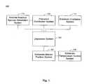
- FIG. 1shows a simplified schematic for process systems according to embodiments of the invention
- FIG. 2Ashows a cross-section of a exemplary process system according to embodiments of the invention
- FIG. 2Bshows a cross-section of another exemplary process system according to embodiment of the invention.
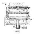
- FIG. 2Cshows another cross-section view of the process system shown in FIG. 2B ;
- FIG. 2Dshows a cross-section of a portion of a deposition chamber that includes a pressure equalization channel and openings in the pumping liner to reduce asymmetric pressure effects according to embodiments of the invention
- FIGS. 3A-Cshow configurations of a top baffle in a process system according to embodiments of the invention
- FIG. 3Dshows a configuration of a top inlet and perforated plate in a process system according to embodiments of the invention
- FIG. 3Eshows a precursor flow distribution for oxygen-containing and silicon-containing precursors in a process system that includes a perforated top plate according to embodiments of the invention
- FIG. 4Ashows a configuration of side nozzles in a process system according to embodiments of the invention
- FIG. 4Bshows another configuration of side nozzles with capped ends and a plurality of opening along the lengths of the nozzle tubes according to embodiments of the invention
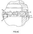
- FIG. 4Cshows a cross-sectional diagram of precursor flow through a capped side nozzle like one that is shown in FIG. 4B ;
- FIG. 4Dshows a design for a one-piece precursor distribution manifold according to embodiments of the invention.
- FIG. 4Eshows an enlarged portion of the precursor distribution manifold shown in FIG. 4D ;
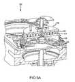
- FIGS. 5A & Bshow cross-sectional views of a process system having a radially concentric configuration of radiative heating elements according to embodiments of the invention
- FIGS. 5C & Dshow cross-sectional views of a process system having a parallel configuration for a plurality of radiative heating elements according to embodiments of the invention
- FIGS. 5E & Fshow cross-sectional views of a process system having a dual socket configuration of radiative heating elements according to embodiments of the invention
- FIG. 6shows an arrangement of deposition, baking and curing chambers according to embodiments of the invention
- FIG. 7Ashows a cross-section of a showerhead with independent gas flow channels according to embodiments of the invention.
- FIG. 7Bshows a cross-section of a showerhead with independent gas flow and plasma zones according to embodiments of the invention
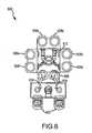
- FIG. 8Ashows a cross-sectional portion of a showerhead where process gases are provided through independent channels that include concentric holes in the faceplate;
- FIG. 8Bshows a picture of the surface of a faceplate having a concentric hole design according to embodiments of the invention.
- FIG. 8Cshows a cross-sectional another cross-sectional portion of a showerhead where process gases are provided through independent parallel channels formed in the faceplate;
- FIG. 8Dshows a cross-sectional portion of a showerhead that flows a process gas from the edge to the center of the showerhead according to embodiments of the invention.
- the systemsmay include a reactive species generation system that supplies reactive radical species to a deposition chamber, where the species chemically react with other deposition precursors and form a flowable film of dielectric on a deposition surface of the substrate.
- a reactive species generation systemthat supplies reactive radical species to a deposition chamber, where the species chemically react with other deposition precursors and form a flowable film of dielectric on a deposition surface of the substrate.
- the systemmay form a layer on a substrate from excited oxygen by a remote plasma source and organo-silane types of precursors.
- the systemsmay also include substrate temperature control systems that can both heat and cool the substrate during a deposition.
- the flowable oxide filmmay be deposited on the substrate surface at low temperature (e.g., less that 100° C.) which is maintained by cooling the substrate during the deposition.
- the temperature control systemmay heat the substrate to perform an anneal.
- the described systemsmay further include substrate motion and positioning systems to rotate the substrate during the deposition and translate it towards or away from the precursor distribution system (e.g., the nozzles and/or showerhead that distribute the precursors in the deposition chamber). Rotation of the substrate may be used to distribute the flowable oxide film more evenly over the substrate surface, similar to a spin-on technique. Translation of the substrate may be used to change the film deposition rate by changing the distance between the substrate deposition surface and the precursors entry into the deposition chamber.
- substrate motion and positioning systemsto rotate the substrate during the deposition and translate it towards or away from the precursor distribution system (e.g., the nozzles and/or showerhead that distribute the precursors in the deposition chamber). Rotation of the substrate may be used to distribute the flowable oxide film more evenly over the substrate surface, similar to a spin-on technique. Translation of the substrate may be used to change the film deposition rate by changing the distance between the substrate deposition surface and the precursors entry into the deposition chamber.
- the systemsmay further have a substrate irradiation system that can irradiate the deposited film with light.
- a substrate irradiation systemthat can irradiate the deposited film with light.
- Embodimentsinclude irradiating the surface with UV light to cure the deposited film, and irradiating the substrate to raise its temperature, for example in a rapid thermal anneal type process.
- FIG. 1provides a simplified schematic of how components of the system 100 can be integrated in embodiments of the invention.
- the system 100includes a deposition system 102 where precursors can chemically react and form a flowable dielectric film (e.g., a silicon oxide film) on a substrate wafer in the deposition chamber.
- the deposition system 102may include coils and/or electrodes that generate radio frequency power inside the deposition chamber to create a plasma. The plasma may enhance the reaction rates of the precursors, which may in turn increases the deposition rate of the flowable dielectric material on the substrate.
- a substrate motion and positioning system 104may be used to rotate the substrate in order to expose different parts of the substrate to the flow of precursors in a more uniform manner. This may make the mass transfer of species in the precursors more uniform. It may also spread low viscosity films more widely over the deposition surface of the substrate.
- the positioning system 104may include or be coupled to a rotatable and vertically translatable substrate pedestal.
- the system 100may also include a substrate temperature control system 106 that is operable to raise and lower the temperature of the substrate.
- the temperature control system 106may be coupled to the substrate pedestal and transfer heat to and from the substrate through direct contact or other thermal coupling of the substrate to the substrate pedestal.
- the temperature system 106may use circulating fluids (e.g., water) to control the substrate temperature, and/or electrical materials (e.g., resistive heating filaments) that supply heat energy by running electric current through the materials.
- the precursors used to form the flowable dielectric filmmay be supplied by a precursor distribution system 108 .
- distribution systems 108include baffle and nozzle systems to flow precursors from the top and sides of the deposition chamber in deposition system 102 .
- Examplesalso include a showerhead with a plurality of openings through which the precursor gases are distributed into the deposition chamber.
- the system 108may include a gas ring without nozzles that has a plurality of openings through which precursors flow into the deposition chamber.
- the distribution system 108may be configured to independently flow two or more precursors into the deposition chamber. In these configurations, at least one pair of the precursors do not contact each other until they exit the distribution system to mix and react in the deposition chamber.
- a reactive species generating system 110may generate a highly reactive species, such as atomic oxygen, which does not mix or react with other precursors, such as a silicon containing precursor, until flowing out of the precursor distribution system 108 and into deposition system 102 .
- the precursors used in system 100may include precursors for forming a flowable dielectric oxide film.
- the oxide film precursorsmay include a reactive species precursor such as radical atomic oxygen, as well as other oxidizing precursors such as molecular oxygen (O 2 ), ozone (O 3 ), water vapor, hydrogen peroxide (H 2 O 2 ), and nitrogen oxides (e.g., N 2 O, NO 2 , etc.) among other oxidizing precursors.
- the oxide film precursorsalso include silicon-containing precursors such as organo-silane compounds including TMOS, TriMOS, TEOS, OMCTS, HMDS, TMCTR, TMCTS, OMTS, TMS, and HMDSO, among others.
- the silicon-containing precursorsmay also include silicon compounds that don't have carbon, such as silane (SiH 4 ).
- dopant precursorsmay also be used such as TEB, TMB, B 2 H 6 , TEPO, PH 3 , P 2 H 6 , and TMP, among other boron and phosphorous dopants.
- the filmis a dielectric silicon nitride or silicon oxynitride, then nitrogen-containing precursors may also be used, such as ammonia, BTBAS, TDMAT, DBEAS, and DADBS, among others.
- halogensmay also be used, for example as catalysts.
- halogen precursorsmay include hydrogen chloride (HCl), and chlorosilanes, such as chloroethylsilane.
- Other acid compoundsmay also be used such as organic acids (e.g., formic acid). All of these deposition precursors may be transported through the distribution system 108 and deposition system 102 by carrier gases, which may include helium, argon, nitrogen (N 2 ), and hydrogen (H 2 ), among other gases.
- the system 100may also include a substrate irradiation system 112 that may bake and/or cure the flowable dielectric material deposited on the substrate surface.
- the irradiation system 112may include one or more lamps that can emit UV light which may be used, for example, to cure the film by decomposing silanol groups in the dielectric material into silicon oxide and water.
- the irradiation systemmay also include heat lamps for baking (i.e., annealing) the flowable films to remove water vapor and other volatile species from the film and make it more dense.
- the system 200includes a deposition chamber 201 where precursors chemically react and deposit a flowable dielectric film on a substrate wafer 202 .
- the wafer 202e.g., a 200 mm, 300 mm, 400 mm, etc. diameter semiconductor substrate wafer
- the wafer 202may coupled to a rotatable substrate pedestal 204 that is also vertically translatable to position the substrate 202 closer or further away from the overlying precursor distribution system 206 .
- the pedestalmay rotate the substrate wafer at a rotational speed of about 1 rpm to about 2000 rpm (e.g., about 10 rpm to about 120 rpm).
- the pedestalmay vertically translate the substrate a distance from, for example, about 0.5 mm to about 100 mm from the side nozzles 208 of the precursor distribution system.
- the precursor distribution system 206includes a plurality of radially distributed side nozzles 208 , each having one of two different lengths.
- the side nozzlesmay eliminated to leave a ring of openings distributed around the wall of the deposition chamber. The precursors flow through these openings into the chamber.
- the distribution system 206may also include a conically-shaped top baffle 210 that may be coaxial with the center of the substrate pedestal 204 .
- a fluid channel 212may run through the center of the baffle 210 to supply a precursor or carrier gas with a different composition than the precursor flowing down the outside directing surface of the baffle.
- the outside surface of the baffle 210may be surrounded by a conduit 214 that directs a reactive precursor from a reactive species generating system (not shown) that is positioned over the deposition chamber 201 .
- the conduit 214may be a straight circular tube with one end opening on the outside surface of baffle 210 and the opposite end coupled to the reactive species generating system.
- the reactive species generating systemmay be a remote plasma generating system (RPS) that generates the reactive species by exposing a more stable starting material to the plasma.
- the starting materialmay be a mixture that includes molecular oxygen (or ozone).
- the exposure of this starting material to a plasma from the RPScauses a portion of the molecular oxygen to dissociate into atomic oxygen, a highly reactive radical species that will chemically react with an organo-silicon precursor (e.g., OMCTS) at much lower temperatures (e.g., less than 100° C.) to form a flowable dielectric on the substrate surface.
- an organo-silicon precursore.g., OMCTS
- the reactive species generated in the reactive species generating systemare often highly reactive with other deposition precursors at even room temperature, they may be transported in an isolated gas mixture down conduit 214 and dispersed into the reaction chamber 201 by baffle 210 before being mixed with other deposition precursors.
- System 200may also include rf coils (not shown) coiled around the dome 216 of the deposition chamber 201 . These coils can create an inductively-coupled plasma in the deposition chamber 201 to further enhance the reactivity of the reactive species precursor and other precursors to deposit the fluid dielectric film on the substrate.
- rf coilscoiled around the dome 216 of the deposition chamber 201 .
- These coilscan create an inductively-coupled plasma in the deposition chamber 201 to further enhance the reactivity of the reactive species precursor and other precursors to deposit the fluid dielectric film on the substrate.
- a gas flow containing reactive atomic oxygen dispersed into the chamber by baffle 210 and an organo-silicon precursor from channel 212 and/or one or more of the side nozzles 208may be directed into a plasma formed above the substrate 202 by the rf coils.
- the atomic oxygen and organo-silicon precursorrapidly react in the plasma even at low temperature to form a highly flowable dielectric film on
- the substrate surface itselfmay be rotated by the pedestal 204 to enhance the uniformity of the deposited film.
- the rotation planemay be parallel to the plane of the wafer deposition surface, or the two planes may be partially out of alignment. When the planes are out of alignment, the rotation of the substrate 204 may create a wobble that can generate fluid turbulence in the space above the deposition surface. In some circumstances, this turbulence may also enhance the uniformity of the dielectric film deposited on the substrate surface.
- the pedestal 204may also include recesses and/or other structures that create a vacuum chuck to hold the wafer in position on the pedestal as it moves. Typical deposition pressures in the chamber range from about 0.05 Torr to about 200 Torr total chamber pressure (e.g., 1 Torr), which makes a vacuum chuck feasible for holding the wafer in position.
- Pedestal rotationmay be actuated by a motor 218 positioned below the deposition chamber 201 and rotationally coupled to a shaft 220 that supports the pedestal 204 .
- the shaft 220may also include internal channels (not shown) that carry cooling fluids and/or electrical wires from cooling/heating systems below the deposition chamber (not shown) to the pedestal 204 . These channels may extend from the center to the periphery of the pedestal to provide uniform cooling and/or heating to the overlying substrate wafer 202 . They also may be designed to operate when the shaft 220 and substrate pedestal 204 are rotating and/or translating. For example, a cooling system may operate to keep the substrate wafer 202 temperature less than 100° C. during the deposition of a flowable oxide film while the pedestal is rotating.
- the system 200may further include an irradiation system 222 positioned above the dome 216 .
- Lamps (not shown) from the irradiation system 222may irradiate the underlying substrate 202 to bake or anneal a deposited film on the substrate.
- the lampsmay also be activated during the deposition to enhance a reaction in the film precursors or deposited film.
- At least the top portion of the dome 216is made from a translucent material capable of transmitting a portion of the light emitted from the lamps.
- FIG. 2Bshows another embodiment of an exemplary processing system 250 where a perforated plate 252 positioned above the side nozzles 253 distributes the precursors from a top inlet 254 .
- the perforated plate 252distributes the precursors through a plurality of openings 260 that traverse the thickness of the plate.
- the plate 252may have, for example from about 10 to 2000 openings (e.g., 200 openings).
- the perforated platemay distribute oxidizing gases, such a atomic oxygen and/or other oxygen-containing gases like TMOS or OMCTS.
- the oxidizing gasis introduced into the deposition chamber above the silicon containing precursors, which are also introduced above the deposition substrate.
- the top inlet 254may have two or more independent precursor (e.g., gas) flow channels 256 and 258 that keep two or more precursors from mixing and reaction until they enter the space above the perforated plate 252 .
- the first flow channel 256may have an annular shape that surrounds the center of inlet 254 . This channel may be coupled to an overlying reactive species generating unit (not shown) that generates a reactive species precursor which flows down the channel 256 and into the space above the perforated plate 252 .
- the second flow channel 258may be cylindrically shaped and may be used to flow a second precursor to the space above the plate 252 . This flow channel may start with a precursor and/or carrier gas source that bypasses a reactive species generating unit. The first and second precursors are then mixed and flow through the openings 260 in the plate 252 to the underlying deposition chamber.
- first flow channel 256may deliver an oxidizing precursor that includes one or more of atomic oxygen (in either a ground or electronically excited state), molecular oxygen (O 2 ), N 2 O, NO, NO 2 , and/or ozone (O 3 ).
- the oxidizing precursormay also include a carrier gas such as helium, argon, nitrogen (N 2 ), etc.
- the second channel 258may also deliver an oxidizing precursor, a carrier gas, and/or an additional gas such as ammonia (NH 3 ).
- the system 250may be configured to heat different parts of the deposition chamber to different temperatures.
- a first heater zonemay heat the top lid 262 and perforated plate 252 to a temperature in a range of about 70° C. to about 300° C. (e.g., about 160° C.).
- a second heater zonemay heat the sidewalls of the deposition chamber above the substrate wafer 264 and pedestal 266 to the same or different temperature than the first heater zone (e.g., up to about 300° C.).
- the system 250may also have a third heater zone below the substrate wafer 264 and pedestal 266 to the same or different temperature than the first and/or second heater zones (e.g., about 70° C. to about 120° C.).
- the pedestal 266may include heating and/or cooling conduits (not shown) inside the pedestal shaft 272 that set the temperature of the pedestal and substrate to from about ⁇ 40° C. to about 200° C. (e.g., about 100° C. to about 160° C., less than about 100° C., about 40° C., etc.).
- the wafer 264may be lifted off the pedestal 266 with lift pins 276 , and may be located about the slit valve door 278 .
- the system 250may additional include a pumping liner 274 (i.e., a pressure equalization channel to compensate for the non-symmetrical location of the pumping port) that includes multiple openings in the plenum of the wafer edge, and/or located on the cylindrical surface around the wafer edge, and/or on the conical shaped surface located around the wafer edge.
- the openingsthemselves may be circular as shown in the liner 274 , or they may be a different shape, such a slot (not shown).
- the openingsmay have a diameter of, for example, about 0.125 inches to about 0.5 inches.
- the pumping liner 274may be above or below the substrate wafer 264 when the wafer is being processed. It may also be located above the slit valve door 278 .
- FIG. 2Cshows another cross-section view of the process system 250 shown in FIG. 2B .
- FIG. 2Cillustrates some dimensions for the system 250 , including a main chamber inner wall diameter ranging from about 10 inches to about 18 inches (e.g., about 15 inches). It also shows a distance between the substrate wafer 264 and the side nozzles of about 0.5 inches to about 8 inches (e.g., about 5.1 inches). In addition, the distance between the substrate wafer 264 and the perforated plate 252 may range from about 0.75 inches to about 12 inches (e.g., about 6.2 inches). Furthermore, the distance between the substrate wafer and the top inside surface of the dome 268 may be about 1 inch to about 16 inches (e.g., about 7.8 inches).
- FIG. 2Dshows a cross-section of a portion of a deposition chamber 280 that includes a pressure equalization channel 282 and openings in the pumping liner 284 .
- the channels 282 and openings 284may be located below an overlying showerhead, top baffle and/or side nozzles, and level with or above the substrate pedestal 286 and wafer 288 .
- the channels 282 and openings 284can reduce asymmetric pressure effects in the chamber. These effects may be caused by the asymmetric location of the pumping port that can create a pressure gradient in the deposition chamber 280 . For example, a pressure gradient underneath the substrate pedestal 286 and/or substrate wafer 288 may cause the pedestal and wafer to tilt, which may cause irregularities in the deposition of the dielectric film.
- the channel 282 and pumping liner openings 284reduce the pressure gradients in the chamber 280 and help stabilize the position of the pedestal 286 and wafer 288 during a deposition.
- FIG. 3Ashows a view of an embodiment of a top portion 302 of the precursor distribution system 206 in FIG. 2A , including channel 212 formed down the center of baffle 210 whose upper portion is surrounded by conduit 214 .
- FIG. 3Ashows a reactive species precursor 304 flowing down conduit 214 and over an outer surface of baffle 210 . As the reactive species precursor 304 reaches the conically shaped end of the baffle 210 closest to the deposition chamber, it gets radially distributed into the chamber, where the reactive species 304 makes first contact with second precursor 306 .
- the second precursor 306may be an organo-silane precursor and may also include a carrier gas.
- the organo-silane precursormay include one or more compounds such as TMOS, TriMOS, TEOS, OMCTS, HMDS, TMCTR, TMCTS, OMTS, TMS, and HMDSO, among other precursors.
- the carrier gasmay include one or more gases such as nitrogen (N 2 ), hydrogen (H 2 ), helium, and argon, among other carrier gases.
- the precursoris fed from a source (not shown) connected to precursor feed line 308 , which is also coupled to channel 212 .
- the second precursor 306may flow down center channel 212 without being exposed to the reactive species 304 that flows over the outside surface of baffle 210 . When the second precursor 306 exits the bottom of baffle 210 into the deposition chamber, it may mix for the first time with the reactive species 304 and additional precursor material supplied by the side nozzles 208 .
- the reactive precursor 304 that flows down conduit 214be generated in a reactive species generation unit (not shown), such as a RPS unit.
- a reactive species generation unitsuch as a RPS unit.
- An RPS unitfor example, can create plasma conditions that are well suited for forming the reactive species. Because the plasma in the RPS unit is remote from a plasma generated in the deposition chamber, different plasma conditions can be used for each component.
- the plasma conditionse.g., rf power, rf frequencies, pressure, temperature, carrier gas partial pressures, etc.
- oxygen precursorssuch as O 2 , O 3 , N 2 O, etc.
- the plasma conditions in the deposition chamberwhere the atomic oxygen reacts with one or more silicon containing precursors (e.g., TMOS, TriMOS, OMCTS, etc.) and forms the flowable dielectric film on the underlying substrate.
- silicon containing precursorse.g., TMOS, TriMOS, OMCTS, etc.
- FIG. 3Ashows a dual-channel top baffle designed to keep the flow of a first and second precursor independent of each other until they reach the deposition chamber.
- Embodiments of the inventionalso include configurations for the independent flow of three or more precursors into the chamber.
- configurationsmay include two or more independent channels like channel 212 running through and inner portion of baffle 210 . Each of these channels may carry precursors that flow independently of each other until reaching the deposition chamber.
- Additional examplesmay include a single-channel baffle 210 that has no channel running through its center.
- second precursor 306enters the deposition chamber from side nozzles 208 and reacts with the reactive precursor 304 radially distributed by baffle 210 into the chamber.
- FIGS. 3B and 3Cshow additional embodiments of the baffle 210 .
- channel 212opens into a conically shaped volume that is defined on its bottom side (i.e., the side closest to the deposition chamber) by a perforated plate 310 a - b .
- the precursorexits this volume through the openings 312 in the perforated plate.
- FIGS. 3B and 3Cshow how the angle between the sidewall and bottom plate 310 a - b can vary.
- the figuresalso illustrate variations in the shape of the outer conical surface over which the precursor flows as it enters the deposition chamber.
- FIG. 3Dshows a configuration of a top inlet 314 and perforated plate 316 that is used in lieu of a top baffle to distribute precursors from the top of a deposition chamber.
- the top inlet 314may have two or more independent precursor flow channels 318 and 320 that keep two or more precursors from mixing and reaction until they enter the space above the perforated plate 316 .
- the first flow channel 318may have an annular shape that surrounds the center of inlet 314 . This channel may be coupled to an overlying reactive species generating unit 322 that generates a reactive species precursor which flows down the channel 318 and into the space above the perforated plate 316 .
- the second flow channel 320may be cylindrically shaped and may be used to flow a second precursor to the space above the plate 316 .
- This flow channelmay start with a precursor and/or carrier gas source that bypasses a reactive species generating unit. The first and second precursors are then mixed and flow through the openings 324 in the plate 316 to the underlying deposition chamber.
- FIG. 3Eshows a precursor flow distribution for oxygen-containing 352 and silicon-containing precursors 354 in a process system 350 that includes a perforated top plate 356 according to embodiments of the invention.
- an oxygen-containing gassuch as radical atomic oxygen is generated by a remote plasma system (not shown) and introduced through the top of the deposition chamber to the space above the perforated plate 356 .
- the reactive oxygen speciesthen flow through openings 358 in the perforated plate 356 down into a region of the chamber where silicon-containing precursors 354 (e.g., organo-silane and/or silanol precursors) are introduced to the chamber by side nozzles 360 .
- silicon-containing precursors 354e.g., organo-silane and/or silanol precursors
- the side nozzles 360 shown in FIG. 3Eare capped at their distal ends extending into the deposition chamber.
- the silicon-containing precursorsexit the side nozzles 360 through a plurality of openings 362 formed in the sidewalls of the nozzle conduits. These openings 362 may be formed in the part of nozzle sidewalls facing the substrate wafer 364 to direct the flow of the silicon-containing precursors 354 towards the wafer.
- the openings 362may be co-linearly aligned to direct the flow of precursor 354 in the same direction, or they may be formed at different radial positions along the sidewalls to direct the precursor flow at different angles with respect to the underlying wafer.
- Embodiments of the capped side nozzles 360include openings 362 with a diameter from about 8 mils to about 200 mils (e.g., about 20 mils to about 80 mils), and a spacing between openings of about 40 mils to about 2 inches (e.g., about 0.25 inches to about 1 inch).
- the number of openings 262may vary with respect to the spacing between openings and/or the length of the side nozzle.
- FIG. 4Ashows a top view of a configuration of side nozzles in a process system 400 according to embodiments of the invention.
- the side nozzlesare radially distributed around the deposition chamber in groups of three nozzles, where the center nozzle 402 extends further into the chamber than two adjacent nozzles 404 . Sixteen of these groups of three are evenly distributed around the deposition chamber, for a total of 48 side nozzles. Additional embodiments includes a total number of nozzles ranging from about 12 to about 80 nozzles.
- the nozzles 402 and 404may be spaced above the deposition surface of the substrate wafer.
- the spacing between the substrate and the nozzlesmay range from, for example, about 1 mm and about 80 mm (e.g., a range of about 10 mm to about 30 mm).
- This distance between the nozzles 402 and 404 and the substratemay vary during the deposition (e.g., the wafer may be vertically translated, as well as rotated and/or agitated, during the deposition).
- the nozzles 402 and 404may all be arranged in the same plane, or different sets of nozzles may be located in different planes.
- the nozzles 402 and 404may be oriented with a centerline parallel to the deposition surface of the wafer, or they may be tilted upwards or downwards with respect to the substrate surface. Different sets of nozzles 402 and 404 may be oriented at different angles with respect to the wafer.
- the nozzles 402 and 404have distal tips extending into the deposition chamber and a proximal ends coupled to the inner diameter surface of an annular gas ring 406 that supplies precursors to the nozzles.
- the gas ringmay have an inner diameter ranging from, for example, from about 10 inches to about 22 inches (e.g., about 14′′ to about 18′′, about 15′′, etc.).
- the distal ends of longer nozzles 402may extend beyond the periphery of the underlying substrate and into the space above the interior of the substrate, while the ends of the shorter nozzles 404 do not reach the substrate periphery. In the embodiment shown in FIG.
- the distal tip of the shorter nozzles 404extend to the periphery of a 12′′ diameter (i.e., 300 mm) substrate wafer, while the distal tips of the longer nozzles 402 extend an additional 4 inches above the interior of the deposition surface.
- the gas ring 406may have one or more internal channels (e.g., 2 to 4 channels) that provide precursors to the nozzles 402 and 404 .
- the internal channelmay provide precursor to all the side nozzles 402 and 404 .
- one channelmay provide precursor to the longer nozzles 402
- the second channelprovides precursors to the shorter nozzles 404 .
- the kinds of reactive deposition precursorse.g., type of organo-silane precursor
- the partial pressures, flow rates of carrier gasesmay be the same or different depending on the deposition recipe.
- FIG. 4Bshows a configuration of capped side nozzles 410 in a process system according to embodiments of the invention. Similar to the side nozzles 360 shown in FIG. 3E above, the nozzles 410 are capped at their distal ends extending into the deposition chamber. Precursors flowing through the nozzles exit through a plurality of openings 412 formed in the sidewalls of the nozzle conduits. These openings 412 may be formed in the part of nozzle sidewalls facing the substrate wafer (not shown) to direct the flow of the precursors towards the wafer. The openings 412 may be co-linearly aligned to direct the flow of precursor in the same direction, or they may be formed at different radial positions along the sidewalls to direct the precursor flow at different angles with respect to the underlying wafer.
- the nozzles 410may be fed by an annular gas ring 414 to which the proximal ends of the nozzles 410 are coupled.
- the gas ring 414may have a single gas flow channel (not shown) to supply the precursor to all the nozzles 410 , or the ring may have a plurality of gas flow channels to supply two or more sets of nozzles 410 .
- a first channelmay supply a first precursor (e.g., a first organosilane precursor) to a first set of nozzles 410 (e.g., the longer set of nozzles shown in FIG. 4B ), and a second channel may supply a second precursor (e.g., a second organosilane precursor) to a second set of nozzles 410 (e.g., the shorter set of nozzles shown in FIG. 4B ).
- a first precursore.g., a first organosilane precursor
- a second precursore.g., a second organ
- FIG. 4Cshows a cross-sectional diagram of precursor flow through a side nozzle 420 like one that is shown in FIG. 4B .
- a precursor 418e.g., an organo-silane vapor precursor in a carrier gas from a vapor delivery system
- the precursor 418flows through the center of the nozzle conduit and exits through openings 422 in the sidewall.
- the openings 422are aligned downwards to direct the flow of precursor 418 towards the underlying wafer substrate (not shown).
- the openings 422may have a diameter from about 8 mils to about 200 mils (e.g., about 20 mils to about 80 mils), and a spacing between openings of about 40 mils to about 2 inches (e.g., about 0.25 inches to about 1 inch).
- the number of openings 422may vary with respect to the spacing between openings and/or the length of the side nozzle 420 .
- Embodiments of the inventionmay also include a single-piece radial precursor manifold that is used in lieu of a set of radial side nozzles like shown in FIG. 4B .
- An illustration of an embodiment of this precursor manifold 450(which may also be referred to as a showerhead) is shown in FIG. 4D .
- the manifold 450includes a plurality of rectangular conduits 452 that are radially distributed around an outer precursor ring 454 .
- the proximal ends of the conduits 452may be coupled to the outer ring 454 , while the distal ends of the conduits 452 are coupled to an inner annular ring 456 .
- the rectangular conduits 452may be supplied with precursor (e.g., one or more organosilicon precursors) by one or more precursor channels (not shown) in the outer precursor ring 454 .
- the precursorexits the conduits 452 though a plurality of openings 462 formed on a side of the conduits.
- the openings 462may have a diameter from about 8 mils to about 200 mils (e.g., about 20 mils to about 80 mils), and a spacing between openings of about 40 mils to about 2 inches (e.g., about 0.25 inches to about 1 inch).
- the number of openings 462may vary with respect to the spacing between openings and/or the length of the conduits 452 .
- FIG. 4Eshows an enlarged portion of the precursor distribution manifold shown in FIG. 4D .
- the radially distributed conduits 452 a - bmay include a first set of conduits 452 a whose length extends to the inner annular ring 456 , and a second set of conduits 452 b whose length extends beyond the inner ring 456 to the center annular ring 460 .
- the first and second sets of conduit 452may be supplied with different mixtures of precursor.
- embodiments of the deposition systemsmay also include irradiation systems for curing and/or heating the flowable dielectric film deposited on the substrate.
- FIGS. 5A and 5Bshow an embodiment of one such irradiation system 500 , which includes a concentric series of annular shaped lamps 502 positioned above a translucent dome 504 and operable to irradiate the underlying substrate 506 .
- the lamps 502may be recessed in a reflective socket 508 whose lamp-side surfaces have a reflective coating that directs more of the light emitted by the lamp towards the substrate 506 .
- the total number of lamps 502may vary from a single lamp to, for example, up to 10 lamps.
- the lamps 502may include UV emitting lamps for a curing processes and/or IR emitting lamps for anneal processes.
- the lamps 502may be tungsten halogen lamps that may have horizontal filaments (i.e., filaments oriented perpendicular to the axis of symmetry of the bulb of the lamp), vertical filaments (i.e., filaments oriented parallel to the axis of symmetry of the bulb), and/or circular filaments.
- Different lamps 502 in the reflective socket 508may have different filament configurations.
- dome 504may include an optically transparent window 510 that allows UV and/or thermal radiation to pass into the deposition chamber.
- the window 510may be made from, for example, quartz, fused silica, aluminum oxy-nitride, or some other suitable translucent material.
- the window 510may be annular in shape and cover the top part of the dome 504 and may have a diameter of, for example, about 8′′ to about 22′′ (e.g., about 14′′).
- the center of the window 510may include an inner opening to allow a conduit to pass through into the top of the deposition chamber.
- the inner openingmay have a diameter of, for example, about 0.5′′ to about 4′′ (e.g., about 1′′ in diameter).
- FIGS. 5C and 5Dshow another configuration for lamps 512 having tubular bulbs that are straight instead of annular shaped.
- the straight lamps 512may be aligned in parallel and recessed in a reflective socket 514 positioned above the transparent window 510 of dome 504 .
- the reflective socket 514may have an annular shape and may match the diameter of the underlying window 510 .
- the ends of the lamps 512may extend beyond the periphery of the socket 514 .
- the number of lamps 512 on either side of the center of window 510may be equal, and about 4 or more lamps (e.g., about 4 to about 10 lamps) may be used.
- FIGS. 5E and 5Fshow another configuration for the irradiation system that has two large lamps 516 positioned on opposite sides around the center of window 510 .
- the large lampsmay be aligned parallel to each other, or at an angle that is less than parallel.
- the lamps 516also may be recessed in a reflective socket 518 that aids in directing a portion of the lamp light towards the substrate in the deposition chamber.
- the embodiments of the irradiation system shown in FIGS. 5A-Fmay be used to irradiate the flowable dielectric film during and/or after its deposition on the substrate surface. It may also be used to irradiate the substrate between deposition steps (e.g., a pulse anneal).
- the waferis positioned on the temperature controlled substrate pedestal.
- the wafer temperaturemay be set to, for example, about ⁇ 40° C. to about 200° C. (e.g., about 40° C.).
- a bakingi.e., annealing
- the temperature of the wafermay increase up to about 1000° C.
- lift-pins on the substrate pedestalmay raise the substrate off the pedestal. This can prevent the pedestal from acting as a heat sink and allow the wafer temperature to be increased at a faster rate (e.g., up to about 100° C./second).
- FIG. 6shows one such system 600 of deposition, baking and curing chambers according to embodiments of the invention.
- a pair of FOOPs 602supply substrate wafers (e.g., 300 mm diameter wafers) that are received by robotic arms 604 and placed into a low pressure holding area 606 before being placed into one of the wafer processing chambers 608 a - f .
- a second robotic arm 610may be used to transport the substrate wafers from the holding area 606 to the processing chambers 608 a - f and back.
- the processing chambers 608 a - fmay include one or more system components for depositing, annealing, curing and/or etching a flowable dielectric film on the substrate wafer.
- two pairs of the processing chambere.g., 608 c - d and 608 e - f
- the third pair of processing chamberse.g., 608 a - b
- the same two pairs of processing chambersmay be configured to both deposit and anneal a flowable dielectric film on the substrate, while the third pair of chambers (e.g., 608 a - b ) may be used for UV or E-beam curing of the deposited film.
- all three pairs of chamberse.g., 608 a - f ) may be configured to deposit an cure a flowable dielectric film on the substrate.
- two pairs of processing chambersmay be used for both deposition and UV or E-beam curing of the flowable dielectric, while a third pair of processing chambers (e.g. 608 a - b ) may be used for annealing the dielectric film.
- a third pair of processing chamberse.g. 608 a - b
- additional configurations of deposition, annealing and curing chambers for flowable dielectric filmsare contemplated by system 600 .
- one or more of the process chambers 608 a - fmay be configured as a wet treatment chamber. These process chambers include heating the flowable dielectric film in an atmosphere that include moisture.
- embodiments of system 600may include wet treatment chambers 608 a - b and anneal processing chambers 608 c - d to perform both wet and dry anneals on the deposited dielectric film.
- Embodiments of gas delivery and plasma generation systems according to the inventionmay include showerheads to distribute precursors into the deposition chamber. These showerheads may be designed so that two or more precursors can independently flow though the showerhead without making contact until mixing in the deposition chamber. The showerheads may also be designed so that plasmas may be independently generated behind the faceplate as well as in the deposition chamber. An independent plasma generated between a blocker plate and faceplate of the showerhead may be used to form a reactive precursor species, as well as improve the efficiency of showerhead cleaning processes by activating cleaning species close to the faceplate. Additional details about showerheads designed to independently flow two or more precursors into a deposition region can be found in U.S.
- FIG. 7Aa simplified cross-sectional schematic of a showerhead system 700 is shown.
- the showerhead 700is configured with two precursor inlet ports 702 and 704 .
- the first precursor inlet port 702is coaxial with the center of the showerhead and defines a flow path for a first precursor down the center of the showerhead and then laterally behind the faceplate 706 .
- the first precursorexits the showerhead into the deposition chamber behind selected openings in the faceplate.
- the second precursor inlet port 704may be configured to flow a second precursor around the first port 702 and into a region 708 between the gasbox 710 and the faceplate 706 .
- the second precursormay then flow from region 708 through selected openings in the faceplate 706 before reaching the deposition region 712 .
- the faceplate 706has two sets of openings: A set of first openings 714 that provide fluid communication between the region 708 and the deposition region, and a second set of openings 716 that provide fluid communication between the first inlet port 702 , the faceplate gap 718 and the deposition region 712 .
- the faceplate 706may be a dual-channel faceplate that keeps the first and second precursors independent until they leave the showerhead for the deposition region.
- the first precursorsmay travel around openings 714 in the faceplate gap 718 before exiting the showerhead through openings 716 .
- Barrierssuch as a cylindrical port may surround the openings 714 to prevent the first precursor from exiting through these openings.
- the second precursors traveling though openings 714cannot flow across the faceplate gap 718 and out second openings 716 into the deposition region.
- the faceplate 706 and pedestal 724may form electrodes to generate a capacitively coupled plasma 726 in the deposition region above the substrate 722 .
- the system 700may also be configured to generate a second plasma 728 behind the in the region 708 behind the face plate.
- this plasma 728may be generated by applying an rf electric field between the gasbox 710 and the faceplate 706 , which form the electrodes for the plasma.
- This plasmamay be made from the second precursor that flows into region 708 from the second precursor inlet port 704 .
- the second plasma 728may be used to generate reactive species from one or more of the precursors in the second precursor mixture.
- the second precursormay include an oxygen containing source that forms radical atomic oxygen species in the plasma 728 .
- the reactive atomic oxygenmay then flow through faceplate openings 714 into the deposition region where they can mix and react with the first precursor material (e.g., an organo-silane precursor).
- the faceplate 706may act as an electrode for both the second plasma 728 and the first plasma 726 in the deposition region.
- This dual-zone plasma systemmay employ simultaneous plasmas to generate a precursor reactive species behind the faceplate 706 , and enhance the reactivity of that species with other precursors in the plasma 726 .
- the plasma 728can be use to activate a cleaning precursor to make it more reactive with materials that have built up in the showerhead openings.
- generating the reactive species in the showerhead instead of the deposition regionmay reduce the number of unwanted reactions between the active cleaning species and the wall of the deposition chamber. For example, more active fluorine species generated behind the faceplate 706 will react before exiting into the deposition region, where they can migrate to aluminum components of the deposition chamber and form unwanted AlF 3 .
- FIGS. 8A and 8Cshow two configurations for a first and second set of openings 804 and 806 in a faceplate 802 through which two precursor mixtures may independently flow before reaching a deposition region.
- FIG. 8Ashows a cross-section for a concentric-opening design in which the first set of openings 804 pass a first precursor through a straight conduit while the second set of openings 806 pass a second precursor though an concentric annular ring opening that surrounds the first opening.
- the first and second precursorsare isolated from each other behind the faceplate and first mix and react when the emerge from the openings 804 and 806 in the deposition region.
- FIG. 8Bis a picture of a portion of faceplate 802 that shows an array of first and second opening 804 , 806 formed in the faceplate surface.
- the second annular openings 806are formed by the gap between the outermost faceplate layer and the tubular walls that define the first openings 804 .
- the annual gap openings 806are about 0.003′′ around the walls of the center openings 804 , which are about 0.028′′ in diameter. Of course, other sizes for the first and second openings may also be used.
- the second precursorpasses through these annular openings 806 and surround the precursor emerging from the center openings 804 .
- FIG. 8Cshows a cross-section for a parallel-opening design in which a first set of openings 808 still creates a straight conduit for a first precursor while a second set of parallel adjacent openings 810 provide an independent flow channel for a second precursor.
- the two sets of openingsare isolated from each other so the first and second precursors do not mix and react until exiting the showerhead into the reaction region.
- the second precursor exiting the openings 810may flow from an edge region of the showerhead to the center as shown in FIG. 8D .
- the channel formed between the second precursor source and the openings 810is fluidly isolated from the first precursor flowing from region 812 though openings 808 into the deposition region.
- the second precursormay be provided by one or more fluid channels formed in and/or around the periphery of the showerhead.
Landscapes
- Chemical & Material Sciences (AREA)
- Engineering & Computer Science (AREA)
- Chemical Kinetics & Catalysis (AREA)
- General Chemical & Material Sciences (AREA)
- Materials Engineering (AREA)
- Mechanical Engineering (AREA)
- Metallurgy (AREA)
- Organic Chemistry (AREA)
- Physics & Mathematics (AREA)
- Plasma & Fusion (AREA)
- Analytical Chemistry (AREA)
- Inorganic Chemistry (AREA)
- Condensed Matter Physics & Semiconductors (AREA)
- General Physics & Mathematics (AREA)
- Manufacturing & Machinery (AREA)
- Computer Hardware Design (AREA)
- Microelectronics & Electronic Packaging (AREA)
- Power Engineering (AREA)
- Chemical Vapour Deposition (AREA)
Abstract
Description
- This application is a continuation of U.S. patent application Ser. No. 14/088,008, filed Nov. 22, 2013, which is a continuation of U.S. patent application Ser. No. 11/754,924, filed May 29, 2007, which claims the benefit of U.S. Provisional Application No. 60/803,499 filed May 30, 2006. This application is also related to co-assigned U.S. Provisional Application No. 60/803,489 by Munro et al, filed May 30, 2006 and titled “A METHOD FOR DEPOSITING AND CURING LOW-K FILMS FOR GAPFILL AND CONFORMAL FILM APPLICATIONS”. This application is also related to co-assigned U.S. Provisional App. No. 60/803,493, by Ingle et al, filed May 30, 2006 and titled “CHEMICAL VAPOR DEPOSITION OF HIGH QUALITY FLOW-LIKE SILICON DIOXIDE USING A SILICON CONTAINING PRECURSOR AND ATOMIC OXYGEN”. This application is also related to U.S. Provisional Application No. 60/803,481, by Chen et al, filed May 30, 2006 and titled “A NOVEL DEPOSITION-PLASMA CURE CYCLE PROCESS TO ENHANCE FILM QUALITY OF SILICON DIOXIDE”. The entire contents of the priority U.S. Provisional patent application and the related applications are herein incorporated by reference for all purposes.
- As integrated circuit chipmakers continue increasing the density of circuit elements on each chip, filling the gaps that separate those elements becomes more challenging. The increased circuit element density has necessitated shorter widths between adjacent elements. As the width of these gaps shrink faster than their height, the ratio of height to width (known as the aspect ratio) proportionally increases. It is more difficult to fill a tall and narrow gap (i.e., a high aspect ratio gap) with a uniform film of dielectric material than a shallow and wide gap (i.e., a low aspect ratio gap).
- One commonly encountered difficulty with filling high aspect ratio gaps is the formation of voids. In high aspect ratio gaps, there is a tendency of the dielectric material filling the gap to deposit at a faster rate around the top end of the gap. Often the dielectric material will close the top before the gap has been completely filled, leaving a void. Even when the top of the gap does not close prematurely, the uneven growth rate of the dielectric film down the sidewalls of the gap can create a weak seam in the middle of the gapfill. These seams can later result in cracks that adversely effect the physical integrity and dielectric properties of the device.
- One technique to avoid the formation of voids and weak seams in dielectric gapfills is to fill the gap at a lower deposition rate. Lower deposition rates can give the dielectric material more time to redistribute on the inside surfaces of the gap to reduce the chances of excessive topside growth. A lower deposition rate may also be the result of increased etching or sputtering that occur at the same time as the dielectric deposition. For example, in HDPCVD dielectric material at the top corners of the gap etch away faster than material on the sidewalls and bottom portion of the gap. This increases the chances that the topside of the gap will remain open so the sidewalls and bottom can completely fill with dielectric material.
- However, reducing the dielectric deposition rate also results in the deposition taking longer to complete. The longer deposition times decrease the rate at which substrate wafers are processed through the deposition chamber, resulting in a reduced efficiency for chamber.
- Another technique to avoid formation of voids and weak seams is to enhance the flowability of the dielectric material that fills the gap. A flowable dielectric material can more easily migrate down the sidewalls and fill in voids at the center of the gap (sometimes referred to as “healing” the voids). Silicon oxide dielectrics are usually made more flowable by increasing the concentration of hydroxyl groups in the dielectric. However, there are challenges both with adding and removing these groups from the oxide without adversely affecting the final quality of the dielectric.
- Thus, there is a need for improved systems and methods for filling short-width, high aspect ratio gaps with a void free dielectric film. These and other problems are addressed by the systems and methods of the present invention.
- Embodiments of the invention include systems to form a dielectric layer on a substrate from a plasma of dielectric precursors. The systems may include a deposition chamber, a substrate stage in the deposition chamber to hold the substrate, and a remote plasma generating system coupled to the deposition chamber, where the plasma generating system is used to generate a dielectric precursor having one or more reactive radicals. The system may also include a precursor distribution system that includes at least one top inlet and a plurality of side inlets for introducing the dielectric precursors to the deposition chamber. The top inlet may be positioned above the substrate stage and the side inlets may be radially distributed around the substrate stage. The reactive radical precursor may be supplied to the deposition chamber through the top inlet. An in-situ plasma generating system may also be included to generate the plasma in the deposition chamber from the dielectric precursors supplied to the deposition chamber.
- Embodiments of the invention also include additional systems to form a silicon dioxide layer on a silicon substrate. These systems may include a deposition chamber, and a substrate stage in the deposition chamber to hold the substrate, where the substrate stage rotates the substrate during the formation of the silicon oxide layer. The systems may also include a remote plasma generating system coupled to the deposition chamber, where the plasma generating system is used to generate an atomic oxygen precursor. They may still further include a precursor distribution system that includes: (i) at least one top inlet, where the top inlet is positioned above the substrate stage, and where the atomic oxygen precursor is supplied to the deposition chamber through the top inlet, and (ii) a plurality of side inlets for introducing one or more silicon-containing precursors to the deposition chamber, where the side inlets are radially distributed around the substrate stage.
- Embodiments of the invention include still further systems to form a dielectric layer on a substrate from a plasma of dielectric precursors. These systems may include a deposition chamber comprising a top side made from a translucent material, a substrate stage in the deposition chamber to hold the substrate, and a remote plasma generating system coupled to the deposition chamber, where the plasma generating system is used to generate a dielectric precursor comprising a reactive radical. The systems may also include a radiative heating system to heat the substrate that includes at least one light source, where at least some of the light emitted from the light source travels through the top side of the deposition chamber before reaching the substrate. In addition, they may include a precursor distribution system that has at least one top inlet and a plurality of side inlets for introducing the dielectric precursors to the deposition chamber. The top inlet is coupled to the top side of the deposition chamber and positioned above the substrate stage, and the side inlets are radially distributed around the substrate stage. The reactive radical precursor may be supplied to the deposition chamber through the top inlet.
- Embodiments of the invention may yet still further include additional systems to form a dielectric layer on a substrate from a plasma of dielectric precursors. The systems may include a deposition chamber, a substrate stage in the deposition chamber to hold the substrate, and a remote plasma generating system coupled to the deposition chamber, where the plasma generating system is used to generate a first dielectric precursor that includes one or more reactive radicals. The systems may also include a precursor distribution system that include a dual-channel showerhead positioned above the substrate stage. The showerhead may include a faceplate with a first set of openings through which the reactive radical precursor enters the deposition chamber, and a second set of openings through which a second dielectric precursor enters the deposition chamber. The precursors may not be mixed until entering the deposition chamber.
- Embodiments of the invention may also include additional systems to form a dielectric layer on a substrate from a plasma of dielectric precursors. The systems may include a deposition chamber, a substrate stage in the deposition chamber to hold the substrate, and a remote plasma generating system coupled to the deposition chamber. The plasma generating system may be used to generate a dielectric precursor comprising a reactive radical. The systems may also include a precursor distribution system that have at least one top inlet, a perforated plate, and a plurality of side inlets for introducing the dielectric precursors to the deposition chamber. The perforated plate may positioned between the top inlet and side inlets, and the side inlets may be radially distributed around the substrate stage. The reactive radical precursor may be distributed in the deposition chamber through openings in the perforated plate. Additionally, an in-situ plasma generating system may be used to generate the plasma in the deposition chamber from the dielectric precursors supplied to the deposition chamber.
- Embodiments of the invention may yet still further include systems to form a dielectric layer on a substrate. The systems may include a deposition chamber, a substrate stage in the deposition chamber to hold the substrate, and a remote plasma generating system coupled to the deposition chamber. The plasma generating system may be used to generate a first dielectric precursor comprising a reactive radical. The systems may also include a precursor distribution system having a plurality of side nozzles for introducing additional dielectric precursors to the deposition chamber. The side nozzles may be radially distributed around the substrate stage, and each of the nozzles may have a plurality of sidewall openings through which the additional dielectric precursors pass to enter the deposition chamber and mix with the first dielectric precursor.
- Embodiments of the invention may also further include additional systems to form a dielectric layer on a substrate. The systems may include a deposition chamber, a substrate stage in the deposition chamber to hold the substrate, and a remote plasma generating system coupled to the deposition chamber. The plasma generating system may be used to generate a first dielectric precursor comprising a reactive radical. The systems may also include a precursor distribution system having a radial precursor manifold for introducing additional dielectric precursors to the deposition chamber, where the manifold may include a plurality of radially distributed conduits positioned above the substrate stage and axially aligned around the substrate stage. The conduits may include a plurality of sidewall openings through which the additional dielectric precursors pass to enter the deposition chamber and mix with the first dielectric precursor.
- Additional embodiments and features are set forth in part in the description that follows, and in part will become apparent to those skilled in the art upon examination of the specification or may be learned by the practice of the invention. The features and advantages of the invention may be realized and attained by means of the instrumentalities, combinations, and methods described in the specification.
FIG. 1 shows a simplified schematic for process systems according to embodiments of the invention;FIG. 2A shows a cross-section of a exemplary process system according to embodiments of the invention;FIG. 2B shows a cross-section of another exemplary process system according to embodiment of the invention;FIG. 2C shows another cross-section view of the process system shown inFIG. 2B ;FIG. 2D shows a cross-section of a portion of a deposition chamber that includes a pressure equalization channel and openings in the pumping liner to reduce asymmetric pressure effects according to embodiments of the invention;FIGS. 3A-C show configurations of a top baffle in a process system according to embodiments of the invention;FIG. 3D shows a configuration of a top inlet and perforated plate in a process system according to embodiments of the invention;FIG. 3E shows a precursor flow distribution for oxygen-containing and silicon-containing precursors in a process system that includes a perforated top plate according to embodiments of the invention;FIG. 4A shows a configuration of side nozzles in a process system according to embodiments of the invention;FIG. 4B shows another configuration of side nozzles with capped ends and a plurality of opening along the lengths of the nozzle tubes according to embodiments of the invention;FIG. 4C shows a cross-sectional diagram of precursor flow through a capped side nozzle like one that is shown inFIG. 4B ;FIG. 4D shows a design for a one-piece precursor distribution manifold according to embodiments of the invention;FIG. 4E shows an enlarged portion of the precursor distribution manifold shown inFIG. 4D ;FIGS. 5A & B show cross-sectional views of a process system having a radially concentric configuration of radiative heating elements according to embodiments of the invention;FIGS. 5C & D show cross-sectional views of a process system having a parallel configuration for a plurality of radiative heating elements according to embodiments of the invention;FIGS. 5E & F show cross-sectional views of a process system having a dual socket configuration of radiative heating elements according to embodiments of the invention;FIG. 6 shows an arrangement of deposition, baking and curing chambers according to embodiments of the invention;FIG. 7A shows a cross-section of a showerhead with independent gas flow channels according to embodiments of the invention;FIG. 7B shows a cross-section of a showerhead with independent gas flow and plasma zones according to embodiments of the invention;FIG. 8A shows a cross-sectional portion of a showerhead where process gases are provided through independent channels that include concentric holes in the faceplate;FIG. 8B shows a picture of the surface of a faceplate having a concentric hole design according to embodiments of the invention;FIG. 8C shows a cross-sectional another cross-sectional portion of a showerhead where process gases are provided through independent parallel channels formed in the faceplate; andFIG. 8D shows a cross-sectional portion of a showerhead that flows a process gas from the edge to the center of the showerhead according to embodiments of the invention.- Systems are described for depositing a flowable CVD dielectric film on a substrate. These dielectric films may be used for STI, IMD, ILD, OCS, and other applications. The systems may include a reactive species generation system that supplies reactive radical species to a deposition chamber, where the species chemically react with other deposition precursors and form a flowable film of dielectric on a deposition surface of the substrate. For example the system may form a layer on a substrate from excited oxygen by a remote plasma source and organo-silane types of precursors. The systems may also include substrate temperature control systems that can both heat and cool the substrate during a deposition. For example, the flowable oxide film may be deposited on the substrate surface at low temperature (e.g., less that 100° C.) which is maintained by cooling the substrate during the deposition. Following the film deposition, the temperature control system may heat the substrate to perform an anneal.
- The described systems may further include substrate motion and positioning systems to rotate the substrate during the deposition and translate it towards or away from the precursor distribution system (e.g., the nozzles and/or showerhead that distribute the precursors in the deposition chamber). Rotation of the substrate may be used to distribute the flowable oxide film more evenly over the substrate surface, similar to a spin-on technique. Translation of the substrate may be used to change the film deposition rate by changing the distance between the substrate deposition surface and the precursors entry into the deposition chamber.
- The systems may further have a substrate irradiation system that can irradiate the deposited film with light. Embodiments include irradiating the surface with UV light to cure the deposited film, and irradiating the substrate to raise its temperature, for example in a rapid thermal anneal type process.
FIG. 1 provides a simplified schematic of how components of thesystem 100 can be integrated in embodiments of the invention. Thesystem 100, includes adeposition system 102 where precursors can chemically react and form a flowable dielectric film (e.g., a silicon oxide film) on a substrate wafer in the deposition chamber. Thedeposition system 102 may include coils and/or electrodes that generate radio frequency power inside the deposition chamber to create a plasma. The plasma may enhance the reaction rates of the precursors, which may in turn increases the deposition rate of the flowable dielectric material on the substrate.- As the flowable oxide is being deposited, a substrate motion and
positioning system 104 may be used to rotate the substrate in order to expose different parts of the substrate to the flow of precursors in a more uniform manner. This may make the mass transfer of species in the precursors more uniform. It may also spread low viscosity films more widely over the deposition surface of the substrate. Thepositioning system 104 may include or be coupled to a rotatable and vertically translatable substrate pedestal. - The
system 100 may also include a substratetemperature control system 106 that is operable to raise and lower the temperature of the substrate. Thetemperature control system 106 may be coupled to the substrate pedestal and transfer heat to and from the substrate through direct contact or other thermal coupling of the substrate to the substrate pedestal. Thetemperature system 106 may use circulating fluids (e.g., water) to control the substrate temperature, and/or electrical materials (e.g., resistive heating filaments) that supply heat energy by running electric current through the materials. - The precursors used to form the flowable dielectric film may be supplied by a
precursor distribution system 108. Examples ofdistribution systems 108 include baffle and nozzle systems to flow precursors from the top and sides of the deposition chamber indeposition system 102. Examples also include a showerhead with a plurality of openings through which the precursor gases are distributed into the deposition chamber. In additional examples, thesystem 108 may include a gas ring without nozzles that has a plurality of openings through which precursors flow into the deposition chamber. - The
distribution system 108 may be configured to independently flow two or more precursors into the deposition chamber. In these configurations, at least one pair of the precursors do not contact each other until they exit the distribution system to mix and react in the deposition chamber. For example, a reactivespecies generating system 110 may generate a highly reactive species, such as atomic oxygen, which does not mix or react with other precursors, such as a silicon containing precursor, until flowing out of theprecursor distribution system 108 and intodeposition system 102. - The precursors used in
system 100 may include precursors for forming a flowable dielectric oxide film. The oxide film precursors may include a reactive species precursor such as radical atomic oxygen, as well as other oxidizing precursors such as molecular oxygen (O2), ozone (O3), water vapor, hydrogen peroxide (H2O2), and nitrogen oxides (e.g., N2O, NO2, etc.) among other oxidizing precursors. The oxide film precursors also include silicon-containing precursors such as organo-silane compounds including TMOS, TriMOS, TEOS, OMCTS, HMDS, TMCTR, TMCTS, OMTS, TMS, and HMDSO, among others. The silicon-containing precursors may also include silicon compounds that don't have carbon, such as silane (SiH4). If the deposited oxide film is a doped oxide film, dopant precursors may also be used such as TEB, TMB, B2H6, TEPO, PH3, P2H6, and TMP, among other boron and phosphorous dopants. If the film is a dielectric silicon nitride or silicon oxynitride, then nitrogen-containing precursors may also be used, such as ammonia, BTBAS, TDMAT, DBEAS, and DADBS, among others. For some film depositions, halogens may also be used, for example as catalysts. These halogen precursors may include hydrogen chloride (HCl), and chlorosilanes, such as chloroethylsilane. Other acid compounds may also be used such as organic acids (e.g., formic acid). All of these deposition precursors may be transported through thedistribution system 108 anddeposition system 102 by carrier gases, which may include helium, argon, nitrogen (N2), and hydrogen (H2), among other gases. - The
system 100 may also include asubstrate irradiation system 112 that may bake and/or cure the flowable dielectric material deposited on the substrate surface. Theirradiation system 112 may include one or more lamps that can emit UV light which may be used, for example, to cure the film by decomposing silanol groups in the dielectric material into silicon oxide and water. The irradiation system may also include heat lamps for baking (i.e., annealing) the flowable films to remove water vapor and other volatile species from the film and make it more dense. - Referring now to
FIG. 2A , a cross-section of anexemplary processing system 200 according to embodiments of the invention is shown. Thesystem 200 includes adeposition chamber 201 where precursors chemically react and deposit a flowable dielectric film on asubstrate wafer 202. The wafer202 (e.g., a 200 mm, 300 mm, 400 mm, etc. diameter semiconductor substrate wafer) may coupled to arotatable substrate pedestal 204 that is also vertically translatable to position thesubstrate 202 closer or further away from the overlyingprecursor distribution system 206. The pedestal may rotate the substrate wafer at a rotational speed of about 1 rpm to about 2000 rpm (e.g., about 10 rpm to about 120 rpm). The pedestal may vertically translate the substrate a distance from, for example, about 0.5 mm to about 100 mm from theside nozzles 208 of the precursor distribution system. - The
precursor distribution system 206 includes a plurality of radially distributedside nozzles 208, each having one of two different lengths. In additional embodiments (not shown) the side nozzles may eliminated to leave a ring of openings distributed around the wall of the deposition chamber. The precursors flow through these openings into the chamber. - The
distribution system 206 may also include a conically-shapedtop baffle 210 that may be coaxial with the center of thesubstrate pedestal 204. Afluid channel 212 may run through the center of thebaffle 210 to supply a precursor or carrier gas with a different composition than the precursor flowing down the outside directing surface of the baffle. - The outside surface of the
baffle 210 may be surrounded by aconduit 214 that directs a reactive precursor from a reactive species generating system (not shown) that is positioned over thedeposition chamber 201. Theconduit 214 may be a straight circular tube with one end opening on the outside surface ofbaffle 210 and the opposite end coupled to the reactive species generating system. - The reactive species generating system may be a remote plasma generating system (RPS) that generates the reactive species by exposing a more stable starting material to the plasma. For example, the starting material may be a mixture that includes molecular oxygen (or ozone). The exposure of this starting material to a plasma from the RPS causes a portion of the molecular oxygen to dissociate into atomic oxygen, a highly reactive radical species that will chemically react with an organo-silicon precursor (e.g., OMCTS) at much lower temperatures (e.g., less than 100° C.) to form a flowable dielectric on the substrate surface. Because the reactive species generated in the reactive species generating system are often highly reactive with other deposition precursors at even room temperature, they may be transported in an isolated gas mixture down
conduit 214 and dispersed into thereaction chamber 201 bybaffle 210 before being mixed with other deposition precursors. System 200 may also include rf coils (not shown) coiled around thedome 216 of thedeposition chamber 201. These coils can create an inductively-coupled plasma in thedeposition chamber 201 to further enhance the reactivity of the reactive species precursor and other precursors to deposit the fluid dielectric film on the substrate. For example, a gas flow containing reactive atomic oxygen dispersed into the chamber bybaffle 210 and an organo-silicon precursor fromchannel 212 and/or one or more of theside nozzles 208 may be directed into a plasma formed above thesubstrate 202 by the rf coils. The atomic oxygen and organo-silicon precursor rapidly react in the plasma even at low temperature to form a highly flowable dielectric film on the substrate surface.- The substrate surface itself may be rotated by the
pedestal 204 to enhance the uniformity of the deposited film. The rotation plane may be parallel to the plane of the wafer deposition surface, or the two planes may be partially out of alignment. When the planes are out of alignment, the rotation of thesubstrate 204 may create a wobble that can generate fluid turbulence in the space above the deposition surface. In some circumstances, this turbulence may also enhance the uniformity of the dielectric film deposited on the substrate surface. Thepedestal 204 may also include recesses and/or other structures that create a vacuum chuck to hold the wafer in position on the pedestal as it moves. Typical deposition pressures in the chamber range from about 0.05 Torr to about 200 Torr total chamber pressure (e.g., 1 Torr), which makes a vacuum chuck feasible for holding the wafer in position. - Pedestal rotation may be actuated by a
motor 218 positioned below thedeposition chamber 201 and rotationally coupled to ashaft 220 that supports thepedestal 204. Theshaft 220 may also include internal channels (not shown) that carry cooling fluids and/or electrical wires from cooling/heating systems below the deposition chamber (not shown) to thepedestal 204. These channels may extend from the center to the periphery of the pedestal to provide uniform cooling and/or heating to theoverlying substrate wafer 202. They also may be designed to operate when theshaft 220 andsubstrate pedestal 204 are rotating and/or translating. For example, a cooling system may operate to keep thesubstrate wafer 202 temperature less than 100° C. during the deposition of a flowable oxide film while the pedestal is rotating. - The
system 200 may further include anirradiation system 222 positioned above thedome 216. Lamps (not shown) from theirradiation system 222 may irradiate theunderlying substrate 202 to bake or anneal a deposited film on the substrate. The lamps may also be activated during the deposition to enhance a reaction in the film precursors or deposited film. At least the top portion of thedome 216 is made from a translucent material capable of transmitting a portion of the light emitted from the lamps. FIG. 2B shows another embodiment of anexemplary processing system 250 where aperforated plate 252 positioned above theside nozzles 253 distributes the precursors from atop inlet 254. Theperforated plate 252 distributes the precursors through a plurality of openings260 that traverse the thickness of the plate. Theplate 252 may have, for example from about 10 to 2000 openings (e.g., 200 openings). In the embodiment shown, the perforated plate may distribute oxidizing gases, such a atomic oxygen and/or other oxygen-containing gases like TMOS or OMCTS. In the illustrated configuration, the oxidizing gas is introduced into the deposition chamber above the silicon containing precursors, which are also introduced above the deposition substrate.- The
top inlet 254 may have two or more independent precursor (e.g., gas)flow channels perforated plate 252. Thefirst flow channel 256 may have an annular shape that surrounds the center ofinlet 254. This channel may be coupled to an overlying reactive species generating unit (not shown) that generates a reactive species precursor which flows down thechannel 256 and into the space above theperforated plate 252. Thesecond flow channel 258 may be cylindrically shaped and may be used to flow a second precursor to the space above theplate 252. This flow channel may start with a precursor and/or carrier gas source that bypasses a reactive species generating unit. The first and second precursors are then mixed and flow through the openings260 in theplate 252 to the underlying deposition chamber. - The
perforated plate 252 andtop inlet 254 may be used to deliver an oxidizing precursor to the underlying space in thedeposition chamber 270. For example,first flow channel 256 may deliver an oxidizing precursor that includes one or more of atomic oxygen (in either a ground or electronically excited state), molecular oxygen (O2), N2O, NO, NO2, and/or ozone (O3). The oxidizing precursor may also include a carrier gas such as helium, argon, nitrogen (N2), etc. Thesecond channel 258 may also deliver an oxidizing precursor, a carrier gas, and/or an additional gas such as ammonia (NH3). - The
system 250 may be configured to heat different parts of the deposition chamber to different temperatures. For example, a first heater zone may heat thetop lid 262 andperforated plate 252 to a temperature in a range of about 70° C. to about 300° C. (e.g., about 160° C.). A second heater zone may heat the sidewalls of the deposition chamber above thesubstrate wafer 264 andpedestal 266 to the same or different temperature than the first heater zone (e.g., up to about 300° C.). Thesystem 250 may also have a third heater zone below thesubstrate wafer 264 andpedestal 266 to the same or different temperature than the first and/or second heater zones (e.g., about 70° C. to about 120° C.). In addition, thepedestal 266 may include heating and/or cooling conduits (not shown) inside thepedestal shaft 272 that set the temperature of the pedestal and substrate to from about −40° C. to about 200° C. (e.g., about 100° C. to about 160° C., less than about 100° C., about 40° C., etc.). During processing, thewafer 264 may be lifted off thepedestal 266 with lift pins276, and may be located about theslit valve door 278. - The
system 250 may additional include a pumping liner274 (i.e., a pressure equalization channel to compensate for the non-symmetrical location of the pumping port) that includes multiple openings in the plenum of the wafer edge, and/or located on the cylindrical surface around the wafer edge, and/or on the conical shaped surface located around the wafer edge. The openings themselves may be circular as shown in theliner 274, or they may be a different shape, such a slot (not shown). The openings may have a diameter of, for example, about 0.125 inches to about 0.5 inches. Thepumping liner 274 may be above or below thesubstrate wafer 264 when the wafer is being processed. It may also be located above theslit valve door 278. FIG. 2C shows another cross-section view of theprocess system 250 shown inFIG. 2B .FIG. 2C illustrates some dimensions for thesystem 250, including a main chamber inner wall diameter ranging from about 10 inches to about 18 inches (e.g., about 15 inches). It also shows a distance between thesubstrate wafer 264 and the side nozzles of about 0.5 inches to about 8 inches (e.g., about 5.1 inches). In addition, the distance between thesubstrate wafer 264 and theperforated plate 252 may range from about 0.75 inches to about 12 inches (e.g., about 6.2 inches). Furthermore, the distance between the substrate wafer and the top inside surface of thedome 268 may be about 1 inch to about 16 inches (e.g., about 7.8 inches).FIG. 2D shows a cross-section of a portion of adeposition chamber 280 that includes apressure equalization channel 282 and openings in thepumping liner 284. In the configuration shown, thechannels 282 andopenings 284 may be located below an overlying showerhead, top baffle and/or side nozzles, and level with or above thesubstrate pedestal 286 andwafer 288.- The
channels 282 andopenings 284 can reduce asymmetric pressure effects in the chamber. These effects may be caused by the asymmetric location of the pumping port that can create a pressure gradient in thedeposition chamber 280. For example, a pressure gradient underneath thesubstrate pedestal 286 and/orsubstrate wafer 288 may cause the pedestal and wafer to tilt, which may cause irregularities in the deposition of the dielectric film. Thechannel 282 andpumping liner openings 284 reduce the pressure gradients in thechamber 280 and help stabilize the position of thepedestal 286 andwafer 288 during a deposition. FIG. 3A shows a view of an embodiment of atop portion 302 of theprecursor distribution system 206 inFIG. 2A , includingchannel 212 formed down the center ofbaffle 210 whose upper portion is surrounded byconduit 214.FIG. 3A shows areactive species precursor 304 flowing downconduit 214 and over an outer surface ofbaffle 210. As thereactive species precursor 304 reaches the conically shaped end of thebaffle 210 closest to the deposition chamber, it gets radially distributed into the chamber, where thereactive species 304 makes first contact withsecond precursor 306.- The
second precursor 306 may be an organo-silane precursor and may also include a carrier gas. The organo-silane precursor may include one or more compounds such as TMOS, TriMOS, TEOS, OMCTS, HMDS, TMCTR, TMCTS, OMTS, TMS, and HMDSO, among other precursors. The carrier gas may include one or more gases such as nitrogen (N2), hydrogen (H2), helium, and argon, among other carrier gases. The precursor is fed from a source (not shown) connected toprecursor feed line 308, which is also coupled tochannel 212. Thesecond precursor 306 may flow downcenter channel 212 without being exposed to thereactive species 304 that flows over the outside surface ofbaffle 210. When thesecond precursor 306 exits the bottom ofbaffle 210 into the deposition chamber, it may mix for the first time with thereactive species 304 and additional precursor material supplied by theside nozzles 208. - The
reactive precursor 304 that flows downconduit 214 be generated in a reactive species generation unit (not shown), such as a RPS unit. An RPS unit, for example, can create plasma conditions that are well suited for forming the reactive species. Because the plasma in the RPS unit is remote from a plasma generated in the deposition chamber, different plasma conditions can be used for each component. For example, the plasma conditions (e.g., rf power, rf frequencies, pressure, temperature, carrier gas partial pressures, etc.) in the RPS unit for forming atomic oxygen radicals from oxygen precursors such as O2, O3, N2O, etc., may be different from the plasma conditions in the deposition chamber where the atomic oxygen reacts with one or more silicon containing precursors (e.g., TMOS, TriMOS, OMCTS, etc.) and forms the flowable dielectric film on the underlying substrate. FIG. 3A shows a dual-channel top baffle designed to keep the flow of a first and second precursor independent of each other until they reach the deposition chamber. Embodiments of the invention also include configurations for the independent flow of three or more precursors into the chamber. For example, configurations may include two or more independent channels likechannel 212 running through and inner portion ofbaffle 210. Each of these channels may carry precursors that flow independently of each other until reaching the deposition chamber. Additional examples may include a single-channel baffle 210 that has no channel running through its center. In these embodiments,second precursor 306 enters the deposition chamber fromside nozzles 208 and reacts with thereactive precursor 304 radially distributed bybaffle 210 into the chamber.FIGS. 3B and 3C show additional embodiments of thebaffle 210. In bothFIGS. 3B and 3C ,channel 212 opens into a conically shaped volume that is defined on its bottom side (i.e., the side closest to the deposition chamber) by a perforated plate310a-b. The precursor exits this volume through theopenings 312 in the perforated plate.FIGS. 3B and 3C , show how the angle between the sidewall and bottom plate310a-bcan vary. The figures also illustrate variations in the shape of the outer conical surface over which the precursor flows as it enters the deposition chamber.FIG. 3D shows a configuration of atop inlet 314 andperforated plate 316 that is used in lieu of a top baffle to distribute precursors from the top of a deposition chamber. In the embodiment shown, thetop inlet 314 may have two or more independentprecursor flow channels perforated plate 316. Thefirst flow channel 318 may have an annular shape that surrounds the center ofinlet 314. This channel may be coupled to an overlying reactivespecies generating unit 322 that generates a reactive species precursor which flows down thechannel 318 and into the space above theperforated plate 316. Thesecond flow channel 320 may be cylindrically shaped and may be used to flow a second precursor to the space above theplate 316. This flow channel may start with a precursor and/or carrier gas source that bypasses a reactive species generating unit. The first and second precursors are then mixed and flow through theopenings 324 in theplate 316 to the underlying deposition chamber.FIG. 3E shows a precursor flow distribution for oxygen-containing352 and silicon-containingprecursors 354 in aprocess system 350 that includes a perforatedtop plate 356 according to embodiments of the invention. LikeFIG. 3D , an oxygen-containing gas such as radical atomic oxygen is generated by a remote plasma system (not shown) and introduced through the top of the deposition chamber to the space above theperforated plate 356. The reactive oxygen species then flow throughopenings 358 in theperforated plate 356 down into a region of the chamber where silicon-containing precursors354 (e.g., organo-silane and/or silanol precursors) are introduced to the chamber byside nozzles 360.- The side nozzles360 shown in
FIG. 3E are capped at their distal ends extending into the deposition chamber. The silicon-containing precursors exit theside nozzles 360 through a plurality ofopenings 362 formed in the sidewalls of the nozzle conduits. Theseopenings 362 may be formed in the part of nozzle sidewalls facing thesubstrate wafer 364 to direct the flow of the silicon-containingprecursors 354 towards the wafer. Theopenings 362 may be co-linearly aligned to direct the flow ofprecursor 354 in the same direction, or they may be formed at different radial positions along the sidewalls to direct the precursor flow at different angles with respect to the underlying wafer. Embodiments of the cappedside nozzles 360 includeopenings 362 with a diameter from about 8 mils to about 200 mils (e.g., about 20 mils to about 80 mils), and a spacing between openings of about 40 mils to about 2 inches (e.g., about 0.25 inches to about 1 inch). The number ofopenings 262 may vary with respect to the spacing between openings and/or the length of the side nozzle. FIG. 4A shows a top view of a configuration of side nozzles in aprocess system 400 according to embodiments of the invention. In the embodiment shown the side nozzles are radially distributed around the deposition chamber in groups of three nozzles, where thecenter nozzle 402 extends further into the chamber than twoadjacent nozzles 404. Sixteen of these groups of three are evenly distributed around the deposition chamber, for a total of 48 side nozzles. Additional embodiments includes a total number of nozzles ranging from about 12 to about 80 nozzles.- The
nozzles nozzles - The
nozzles nozzles nozzles - The
nozzles annular gas ring 406 that supplies precursors to the nozzles. The gas ring may have an inner diameter ranging from, for example, from about 10 inches to about 22 inches (e.g., about 14″ to about 18″, about 15″, etc.). In some configurations, the distal ends oflonger nozzles 402 may extend beyond the periphery of the underlying substrate and into the space above the interior of the substrate, while the ends of theshorter nozzles 404 do not reach the substrate periphery. In the embodiment shown inFIG. 4 , the distal tip of theshorter nozzles 404 extend to the periphery of a 12″ diameter (i.e., 300 mm) substrate wafer, while the distal tips of thelonger nozzles 402 extend an additional 4 inches above the interior of the deposition surface. - The
gas ring 406 may have one or more internal channels (e.g., 2 to 4 channels) that provide precursors to thenozzles side nozzles longer nozzles 402, while the second channel provides precursors to theshorter nozzles 404. For each channel the kinds of reactive deposition precursors (e.g., type of organo-silane precursor) and/or the partial pressures, flow rates of carrier gases, may be the same or different depending on the deposition recipe. FIG. 4B shows a configuration of cappedside nozzles 410 in a process system according to embodiments of the invention. Similar to theside nozzles 360 shown inFIG. 3E above, thenozzles 410 are capped at their distal ends extending into the deposition chamber. Precursors flowing through the nozzles exit through a plurality of openings412 formed in the sidewalls of the nozzle conduits. These openings412 may be formed in the part of nozzle sidewalls facing the substrate wafer (not shown) to direct the flow of the precursors towards the wafer. The openings412 may be co-linearly aligned to direct the flow of precursor in the same direction, or they may be formed at different radial positions along the sidewalls to direct the precursor flow at different angles with respect to the underlying wafer.- The
nozzles 410 may be fed by anannular gas ring 414 to which the proximal ends of thenozzles 410 are coupled. Thegas ring 414 may have a single gas flow channel (not shown) to supply the precursor to all thenozzles 410, or the ring may have a plurality of gas flow channels to supply two or more sets ofnozzles 410. For example, in a dual-channel gas ring design, a first channel may supply a first precursor (e.g., a first organosilane precursor) to a first set of nozzles410 (e.g., the longer set of nozzles shown inFIG. 4B ), and a second channel may supply a second precursor (e.g., a second organosilane precursor) to a second set of nozzles410 (e.g., the shorter set of nozzles shown inFIG. 4B ). FIG. 4C shows a cross-sectional diagram of precursor flow through aside nozzle 420 like one that is shown inFIG. 4B . A precursor418 (e.g., an organo-silane vapor precursor in a carrier gas from a vapor delivery system) is supplied by aprecursor flow channel 416 coupled to the proximal end of theside nozzle 420. Theprecursor 418 flows through the center of the nozzle conduit and exits throughopenings 422 in the sidewall. In the nozzle configuration shown, theopenings 422 are aligned downwards to direct the flow ofprecursor 418 towards the underlying wafer substrate (not shown). Theopenings 422 may have a diameter from about 8 mils to about 200 mils (e.g., about 20 mils to about 80 mils), and a spacing between openings of about 40 mils to about 2 inches (e.g., about 0.25 inches to about 1 inch). The number ofopenings 422 may vary with respect to the spacing between openings and/or the length of theside nozzle 420.- Embodiments of the invention may also include a single-piece radial precursor manifold that is used in lieu of a set of radial side nozzles like shown in
FIG. 4B . An illustration of an embodiment of this precursor manifold450 (which may also be referred to as a showerhead) is shown inFIG. 4D . The manifold450 includes a plurality ofrectangular conduits 452 that are radially distributed around anouter precursor ring 454. The proximal ends of theconduits 452 may be coupled to theouter ring 454, while the distal ends of theconduits 452 are coupled to an innerannular ring 456. - The
rectangular conduits 452 may be supplied with precursor (e.g., one or more organosilicon precursors) by one or more precursor channels (not shown) in theouter precursor ring 454. The precursor exits theconduits 452 though a plurality ofopenings 462 formed on a side of the conduits. Theopenings 462 may have a diameter from about 8 mils to about 200 mils (e.g., about 20 mils to about 80 mils), and a spacing between openings of about 40 mils to about 2 inches (e.g., about 0.25 inches to about 1 inch). The number ofopenings 462 may vary with respect to the spacing between openings and/or the length of theconduits 452. FIG. 4E shows an enlarged portion of the precursor distribution manifold shown inFIG. 4D . In the embodiment shown, the radially distributedconduits 452a-bmay include a first set ofconduits 452awhose length extends to the innerannular ring 456, and a second set ofconduits 452bwhose length extends beyond theinner ring 456 to the centerannular ring 460. The first and second sets ofconduit 452 may be supplied with different mixtures of precursor.- As noted above, embodiments of the deposition systems may also include irradiation systems for curing and/or heating the flowable dielectric film deposited on the substrate.
FIGS. 5A and 5B show an embodiment of onesuch irradiation system 500, which includes a concentric series of annular shapedlamps 502 positioned above atranslucent dome 504 and operable to irradiate theunderlying substrate 506. Thelamps 502 may be recessed in areflective socket 508 whose lamp-side surfaces have a reflective coating that directs more of the light emitted by the lamp towards thesubstrate 506. The total number oflamps 502 may vary from a single lamp to, for example, up to 10 lamps. - The
lamps 502 may include UV emitting lamps for a curing processes and/or IR emitting lamps for anneal processes. For example, thelamps 502 may be tungsten halogen lamps that may have horizontal filaments (i.e., filaments oriented perpendicular to the axis of symmetry of the bulb of the lamp), vertical filaments (i.e., filaments oriented parallel to the axis of symmetry of the bulb), and/or circular filaments.Different lamps 502 in thereflective socket 508 may have different filament configurations. - Light from the
lamps 502 is transmitted through thedome 504 and onto the substrate deposition surface. At least a portion ofdome 504 may include an opticallytransparent window 510 that allows UV and/or thermal radiation to pass into the deposition chamber. Thewindow 510 may be made from, for example, quartz, fused silica, aluminum oxy-nitride, or some other suitable translucent material. As shown inFIGS. 5A-F , thewindow 510 may be annular in shape and cover the top part of thedome 504 and may have a diameter of, for example, about 8″ to about 22″ (e.g., about 14″). The center of thewindow 510 may include an inner opening to allow a conduit to pass through into the top of the deposition chamber. The inner opening may have a diameter of, for example, about 0.5″ to about 4″ (e.g., about 1″ in diameter). FIGS. 5C and 5D show another configuration forlamps 512 having tubular bulbs that are straight instead of annular shaped. Thestraight lamps 512 may be aligned in parallel and recessed in areflective socket 514 positioned above thetransparent window 510 ofdome 504. Thereflective socket 514 may have an annular shape and may match the diameter of theunderlying window 510. The ends of thelamps 512 may extend beyond the periphery of thesocket 514. The number oflamps 512 on either side of the center ofwindow 510 may be equal, and about 4 or more lamps (e.g., about 4 to about 10 lamps) may be used.FIGS. 5E and 5F show another configuration for the irradiation system that has twolarge lamps 516 positioned on opposite sides around the center ofwindow 510. The large lamps may be aligned parallel to each other, or at an angle that is less than parallel. Thelamps 516 also may be recessed in areflective socket 518 that aids in directing a portion of the lamp light towards the substrate in the deposition chamber.- The embodiments of the irradiation system shown in
FIGS. 5A-F may be used to irradiate the flowable dielectric film during and/or after its deposition on the substrate surface. It may also be used to irradiate the substrate between deposition steps (e.g., a pulse anneal). During the film deposition, the wafer is positioned on the temperature controlled substrate pedestal. The wafer temperature may be set to, for example, about −40° C. to about 200° C. (e.g., about 40° C.). When the substrate is irradiated in a baking (i.e., annealing) process, the temperature of the wafer may increase up to about 1000° C. During this high-temperature anneal, lift-pins on the substrate pedestal may raise the substrate off the pedestal. This can prevent the pedestal from acting as a heat sink and allow the wafer temperature to be increased at a faster rate (e.g., up to about 100° C./second). - Embodiments of the deposition systems may be incorporated into larger fabrication systems for producing integrated circuit chips.
FIG. 6 shows onesuch system 600 of deposition, baking and curing chambers according to embodiments of the invention. In the figure, a pair ofFOOPs 602 supply substrate wafers (e.g., 300 mm diameter wafers) that are received byrobotic arms 604 and placed into a lowpressure holding area 606 before being placed into one of the wafer processing chambers608a-f. A secondrobotic arm 610 may be used to transport the substrate wafers from the holdingarea 606 to the processing chambers608a-fand back. - The processing chambers608a-fmay include one or more system components for depositing, annealing, curing and/or etching a flowable dielectric film on the substrate wafer. In one configuration, two pairs of the processing chamber (e.g.,608c-dand608e-f) may be used to deposit the flowable dielectric material on the substrate, and the third pair of processing chambers (e.g.,608a-b) may be used to anneal the deposited dielectric. In another configuration, the same two pairs of processing chambers (e.g.,608c-dand608e-f) may be configured to both deposit and anneal a flowable dielectric film on the substrate, while the third pair of chambers (e.g.,608a-b) may be used for UV or E-beam curing of the deposited film. In still another configuration, all three pairs of chambers (e.g.,608a-f) may be configured to deposit an cure a flowable dielectric film on the substrate. In yet another configuration, two pairs of processing chambers (e.g.,608c-dand608e-f) may be used for both deposition and UV or E-beam curing of the flowable dielectric, while a third pair of processing chambers (e.g.608a-b) may be used for annealing the dielectric film. It will be appreciated, that additional configurations of deposition, annealing and curing chambers for flowable dielectric films are contemplated by
system 600. - In addition, one or more of the process chambers608a-fmay be configured as a wet treatment chamber. These process chambers include heating the flowable dielectric film in an atmosphere that include moisture. Thus, embodiments of
system 600 may include wet treatment chambers608a-bandanneal processing chambers 608c-dto perform both wet and dry anneals on the deposited dielectric film. - Embodiments of gas delivery and plasma generation systems according to the invention may include showerheads to distribute precursors into the deposition chamber. These showerheads may be designed so that two or more precursors can independently flow though the showerhead without making contact until mixing in the deposition chamber. The showerheads may also be designed so that plasmas may be independently generated behind the faceplate as well as in the deposition chamber. An independent plasma generated between a blocker plate and faceplate of the showerhead may be used to form a reactive precursor species, as well as improve the efficiency of showerhead cleaning processes by activating cleaning species close to the faceplate. Additional details about showerheads designed to independently flow two or more precursors into a deposition region can be found in U.S. patent application Ser. No. 11/040,712 to Jung et al, filed Jan. 22, 2005, and titled “MIXING ENERGIZED AND NON-ENERGIZED GASES FOR SILICON NITRIDE DEPOSITION” the entire contents of which are herein incorporated by reference for all purposes.
- Referring now to
FIG. 7A , a simplified cross-sectional schematic of ashowerhead system 700 is shown. Theshowerhead 700 is configured with twoprecursor inlet ports precursor inlet port 702 is coaxial with the center of the showerhead and defines a flow path for a first precursor down the center of the showerhead and then laterally behind thefaceplate 706. The first precursor exits the showerhead into the deposition chamber behind selected openings in the faceplate. - The second
precursor inlet port 704 may be configured to flow a second precursor around thefirst port 702 and into aregion 708 between thegasbox 710 and thefaceplate 706. The second precursor may then flow fromregion 708 through selected openings in thefaceplate 706 before reaching thedeposition region 712. AsFIG. 7A shows, thefaceplate 706 has two sets of openings: A set offirst openings 714 that provide fluid communication between theregion 708 and the deposition region, and a second set ofopenings 716 that provide fluid communication between thefirst inlet port 702, thefaceplate gap 718 and thedeposition region 712. - The
faceplate 706 may be a dual-channel faceplate that keeps the first and second precursors independent until they leave the showerhead for the deposition region. For example, the first precursors may travel aroundopenings 714 in thefaceplate gap 718 before exiting the showerhead throughopenings 716. Barriers such as a cylindrical port may surround theopenings 714 to prevent the first precursor from exiting through these openings. Likewise, the second precursors traveling thoughopenings 714 cannot flow across thefaceplate gap 718 and outsecond openings 716 into the deposition region. - When the precursors exit their respective sets of openings they can mix in the
deposition region 712 above thesubstrate wafer 722 andsubstrate pedestal 724. Thefaceplate 706 andpedestal 724 may form electrodes to generate a capacitively coupledplasma 726 in the deposition region above thesubstrate 722. - The
system 700 may also be configured to generate asecond plasma 728 behind the in theregion 708 behind the face plate. AsFIG. 7B shows, thisplasma 728 may be generated by applying an rf electric field between thegasbox 710 and thefaceplate 706, which form the electrodes for the plasma. This plasma may be made from the second precursor that flows intoregion 708 from the secondprecursor inlet port 704. Thesecond plasma 728 may be used to generate reactive species from one or more of the precursors in the second precursor mixture. For example, the second precursor may include an oxygen containing source that forms radical atomic oxygen species in theplasma 728. The reactive atomic oxygen may then flow throughfaceplate openings 714 into the deposition region where they can mix and react with the first precursor material (e.g., an organo-silane precursor). - In
FIG. 7B , thefaceplate 706 may act as an electrode for both thesecond plasma 728 and thefirst plasma 726 in the deposition region. This dual-zone plasma system may employ simultaneous plasmas to generate a precursor reactive species behind thefaceplate 706, and enhance the reactivity of that species with other precursors in theplasma 726. In addition, theplasma 728 can be use to activate a cleaning precursor to make it more reactive with materials that have built up in the showerhead openings. In addition, generating the reactive species in the showerhead instead of the deposition region may reduce the number of unwanted reactions between the active cleaning species and the wall of the deposition chamber. For example, more active fluorine species generated behind thefaceplate 706 will react before exiting into the deposition region, where they can migrate to aluminum components of the deposition chamber and form unwanted AlF3. FIGS. 8A and 8C show two configurations for a first and second set ofopenings faceplate 802 through which two precursor mixtures may independently flow before reaching a deposition region.FIG. 8A shows a cross-section for a concentric-opening design in which the first set ofopenings 804 pass a first precursor through a straight conduit while the second set ofopenings 806 pass a second precursor though an concentric annular ring opening that surrounds the first opening. The first and second precursors are isolated from each other behind the faceplate and first mix and react when the emerge from theopenings FIG. 8B is a picture of a portion offaceplate 802 that shows an array of first andsecond opening annular openings 806 are formed by the gap between the outermost faceplate layer and the tubular walls that define thefirst openings 804. In the embodiment shown in the picture, theannual gap openings 806 are about 0.003″ around the walls of thecenter openings 804, which are about 0.028″ in diameter. Of course, other sizes for the first and second openings may also be used. The second precursor passes through theseannular openings 806 and surround the precursor emerging from thecenter openings 804.FIG. 8C shows a cross-section for a parallel-opening design in which a first set ofopenings 808 still creates a straight conduit for a first precursor while a second set of paralleladjacent openings 810 provide an independent flow channel for a second precursor. The two sets of openings are isolated from each other so the first and second precursors do not mix and react until exiting the showerhead into the reaction region.- The second precursor exiting the
openings 810 may flow from an edge region of the showerhead to the center as shown inFIG. 8D . The channel formed between the second precursor source and theopenings 810 is fluidly isolated from the first precursor flowing fromregion 812 thoughopenings 808 into the deposition region. The second precursor may be provided by one or more fluid channels formed in and/or around the periphery of the showerhead. - Where a range of values is provided, it is understood that each intervening value, to the tenth of the unit of the lower limit unless the context clearly dictates otherwise, between the upper and lower limits of that range is also specifically disclosed. Each smaller range between any stated value or intervening value in a stated range and any other stated or intervening value in that stated range is encompassed within the invention. The upper and lower limits of these smaller ranges may independently be included or excluded in the range, and each range where either, neither or both limits are included in the smaller ranges is also encompassed within the invention, subject to any specifically excluded limit in the stated range. Where the stated range includes one or both of the limits, ranges excluding either or both of those included limits are also included in the invention.
- As used herein and in the appended claims, the singular forms “a”, “and”, and “the” include plural referents unless the context clearly dictates otherwise. Thus, for example, reference to “a process” may includes a plurality of such processes and reference to “the nozzle” may include reference to one or more nozzles and equivalents thereof known to those skilled in the art, and so forth.
- Also, the words “comprise,” “comprising,” “include,” “including,” and “includes” when used in this specification and in the following claims are intended to specify the presence of stated features, integers, components, or steps, but they do not preclude the presence or addition of one or more other features, integers, components, steps, or groups.
Claims (20)
1. A substrate processing system comprising:
a processing chamber;
a first electrode;
a pedestal, wherein the pedestal is electrically coupled with ground and configured to operate as a second electrode;
a faceplate;
a first plasma region, wherein the first plasma region is at least partially defined from above by the first electrode and at least partially defined from below by the faceplate; and
a second plasma region, wherein the second plasma region is at least partially defined from above by the faceplate and at least partially defined from below by the pedestal,
wherein the faceplate defines a first plurality of apertures providing fluid access from the first plasma region to the second plasma region, wherein the faceplate defines a second plurality of apertures providing fluid access to the second plasma region without exposure to the first plasma region, and wherein the second plurality of apertures are fluidly accessed from a radial edge of the faceplate.
2. The substrate processing system ofclaim 1 , wherein the faceplate separates the first plasma region from the second plasma region in the processing chamber.
3. The substrate processing system ofclaim 1 , wherein the faceplate comprises a third electrode that is shared between the first plasma region and the second plasma region.
4. The substrate processing system ofclaim 1 , wherein the first electrode and the faceplate are configured to generate an RF plasma in the first plasma region.
5. The substrate processing system ofclaim 1 , wherein the faceplate and the second electrode are configured generate an RF plasma in the second plasma region.
6. The substrate processing system ofclaim 1 , further comprising a distribution plate positioned between the first electrode and the faceplate.
7. The substrate processing system ofclaim 6 , wherein the distribution plate is electrically coupled with the first electrode.
8. The substrate processing system ofclaim 1 , wherein the substrate processing system further comprises a gas inlet configured to supply a first precursor to the first plasma region.
9. The substrate processing system ofclaim 8 , wherein the gas inlet is further configured to provide a second precursor through the gas inlet fluidly separate from the first precursor.
10. The substrate processing system ofclaim 1 , wherein each aperture of the second plurality of apertures is coaxially aligned with an aperture of the first plurality of apertures.
11. The substrate processing system ofclaim 1 , wherein each aperture of the first plurality of apertures is characterized by a first diameter fluidly accessed from the first plasma region and a second diameter less than the first fluidly accessing the second plasma region.
12. The substrate processing system ofclaim 1 , wherein the system further comprises a temperature control system configured to maintain the pedestal at a temperature ranging from about −40° C. to about 200° C.
13. A substrate processing chamber comprising:
an inlet assembly;
a first electrode defining a central channel within which the inlet assembly is at least partially disposed;
a pedestal, wherein the pedestal is electrically coupled with ground and configured to operate as a second electrode;
a faceplate;
a first plasma region, wherein the first plasma region is at least partially defined from above by the first electrode and at least partially defined from below by the faceplate; and
a second plasma region, wherein the second plasma region is at least partially defined from above by the faceplate and at least partially defined from below by the pedestal,
wherein the faceplate defines a first plurality of apertures providing fluid access from the first plasma region to the second plasma region, wherein the faceplate defines a second plurality of apertures providing fluid access to the second plasma region without exposure to the first plasma region, and wherein the second plurality of apertures are fluidly accessed from a radial edge of the faceplate.
14. The substrate processing chamber ofclaim 13 , wherein the faceplate is electrically operable as a third electrode that is shared between the first plasma region and the second plasma region.
15. The substrate processing chamber ofclaim 14 , wherein the faceplate is switchably coupled with a power source and ground.
16. The substrate processing chamber ofclaim 13 , wherein the first electrode and the faceplate are electrically operable to generate an RF plasma in the first plasma region.
17. The substrate processing chamber ofclaim 13 , wherein the faceplate and the second electrode are electrically operable to generate an RF plasma in the second plasma region.
18. The substrate processing chamber ofclaim 13 , further comprising a distribution plate positioned between the first electrode and the faceplate.
19. The substrate processing chamber ofclaim 18 , wherein the distribution plate is electrically coupled with the first electrode.
20. The substrate processing chamber ofclaim 13 , wherein the chamber further comprises a temperature control system that maintains the pedestal at a temperature ranging from about −40° C. to about 200° C.
Priority Applications (1)
| Application Number | Priority Date | Filing Date | Title |
|---|---|---|---|
| US15/581,324US20170226637A1 (en) | 2006-05-30 | 2017-04-28 | Process chamber for dielectric gapfill |
Applications Claiming Priority (4)
| Application Number | Priority Date | Filing Date | Title |
|---|---|---|---|
| US80349906P | 2006-05-30 | 2006-05-30 | |
| US11/754,924US20070281106A1 (en) | 2006-05-30 | 2007-05-29 | Process chamber for dielectric gapfill |
| US14/088,008US20140083362A1 (en) | 2006-05-30 | 2013-11-22 | Process chamber for dielectric gapfill |
| US15/581,324US20170226637A1 (en) | 2006-05-30 | 2017-04-28 | Process chamber for dielectric gapfill |
Related Parent Applications (1)
| Application Number | Title | Priority Date | Filing Date |
|---|---|---|---|
| US14/088,008ContinuationUS20140083362A1 (en) | 2006-05-30 | 2013-11-22 | Process chamber for dielectric gapfill |
Publications (1)
| Publication Number | Publication Date |
|---|---|
| US20170226637A1true US20170226637A1 (en) | 2017-08-10 |
Family
ID=38779453
Family Applications (4)
| Application Number | Title | Priority Date | Filing Date |
|---|---|---|---|
| US11/754,924AbandonedUS20070281106A1 (en) | 2006-05-30 | 2007-05-29 | Process chamber for dielectric gapfill |
| US13/248,567AbandonedUS20120073501A1 (en) | 2006-05-30 | 2011-09-29 | Process chamber for dielectric gapfill |
| US14/088,008AbandonedUS20140083362A1 (en) | 2006-05-30 | 2013-11-22 | Process chamber for dielectric gapfill |
| US15/581,324AbandonedUS20170226637A1 (en) | 2006-05-30 | 2017-04-28 | Process chamber for dielectric gapfill |
Family Applications Before (3)
| Application Number | Title | Priority Date | Filing Date |
|---|---|---|---|
| US11/754,924AbandonedUS20070281106A1 (en) | 2006-05-30 | 2007-05-29 | Process chamber for dielectric gapfill |
| US13/248,567AbandonedUS20120073501A1 (en) | 2006-05-30 | 2011-09-29 | Process chamber for dielectric gapfill |
| US14/088,008AbandonedUS20140083362A1 (en) | 2006-05-30 | 2013-11-22 | Process chamber for dielectric gapfill |
Country Status (6)
| Country | Link |
|---|---|
| US (4) | US20070281106A1 (en) |
| EP (1) | EP2022087A4 (en) |
| KR (1) | KR101207525B1 (en) |
| SG (1) | SG172648A1 (en) |
| TW (1) | TWI397122B (en) |
| WO (1) | WO2007140425A2 (en) |
Cited By (97)
| Publication number | Priority date | Publication date | Assignee | Title |
|---|---|---|---|---|
| US9865484B1 (en) | 2016-06-29 | 2018-01-09 | Applied Materials, Inc. | Selective etch using material modification and RF pulsing |
| US9881805B2 (en) | 2015-03-02 | 2018-01-30 | Applied Materials, Inc. | Silicon selective removal |
| US9934942B1 (en) | 2016-10-04 | 2018-04-03 | Applied Materials, Inc. | Chamber with flow-through source |
| US9947549B1 (en) | 2016-10-10 | 2018-04-17 | Applied Materials, Inc. | Cobalt-containing material removal |
| US9966240B2 (en) | 2014-10-14 | 2018-05-08 | Applied Materials, Inc. | Systems and methods for internal surface conditioning assessment in plasma processing equipment |
| US9978564B2 (en) | 2012-09-21 | 2018-05-22 | Applied Materials, Inc. | Chemical control features in wafer process equipment |
| US10008428B2 (en) | 2012-11-08 | 2018-06-26 | Novellus Systems, Inc. | Methods for depositing films on sensitive substrates |
| US10026621B2 (en) | 2016-11-14 | 2018-07-17 | Applied Materials, Inc. | SiN spacer profile patterning |
| US10032606B2 (en) | 2012-08-02 | 2018-07-24 | Applied Materials, Inc. | Semiconductor processing with DC assisted RF power for improved control |
| US10037884B2 (en) | 2016-08-31 | 2018-07-31 | Lam Research Corporation | Selective atomic layer deposition for gapfill using sacrificial underlayer |
| US10043657B2 (en)* | 2010-04-15 | 2018-08-07 | Lam Research Corporation | Plasma assisted atomic layer deposition metal oxide for patterning applications |
| US10043655B2 (en) | 2010-04-15 | 2018-08-07 | Novellus Systems, Inc. | Plasma activated conformal dielectric film deposition |
| US10043684B1 (en) | 2017-02-06 | 2018-08-07 | Applied Materials, Inc. | Self-limiting atomic thermal etching systems and methods |
| US10043674B1 (en) | 2017-08-04 | 2018-08-07 | Applied Materials, Inc. | Germanium etching systems and methods |
| US10049891B1 (en) | 2017-05-31 | 2018-08-14 | Applied Materials, Inc. | Selective in situ cobalt residue removal |
| US10062578B2 (en) | 2011-03-14 | 2018-08-28 | Applied Materials, Inc. | Methods for etch of metal and metal-oxide films |
| US10062587B2 (en) | 2012-07-18 | 2018-08-28 | Applied Materials, Inc. | Pedestal with multi-zone temperature control and multiple purge capabilities |
| US10062579B2 (en) | 2016-10-07 | 2018-08-28 | Applied Materials, Inc. | Selective SiN lateral recess |
| US10062585B2 (en) | 2016-10-04 | 2018-08-28 | Applied Materials, Inc. | Oxygen compatible plasma source |
| US10062575B2 (en) | 2016-09-09 | 2018-08-28 | Applied Materials, Inc. | Poly directional etch by oxidation |
| US10062563B2 (en) | 2016-07-01 | 2018-08-28 | Lam Research Corporation | Selective atomic layer deposition with post-dose treatment |
| US10128086B1 (en) | 2017-10-24 | 2018-11-13 | Applied Materials, Inc. | Silicon pretreatment for nitride removal |
| US10147620B2 (en) | 2015-08-06 | 2018-12-04 | Applied Materials, Inc. | Bolted wafer chuck thermal management systems and methods for wafer processing systems |
| US10163696B2 (en) | 2016-11-11 | 2018-12-25 | Applied Materials, Inc. | Selective cobalt removal for bottom up gapfill |
| US10170336B1 (en) | 2017-08-04 | 2019-01-01 | Applied Materials, Inc. | Methods for anisotropic control of selective silicon removal |
| US10186428B2 (en) | 2016-11-11 | 2019-01-22 | Applied Materials, Inc. | Removal methods for high aspect ratio structures |
| US10224210B2 (en) | 2014-12-09 | 2019-03-05 | Applied Materials, Inc. | Plasma processing system with direct outlet toroidal plasma source |
| US10242908B2 (en) | 2016-11-14 | 2019-03-26 | Applied Materials, Inc. | Airgap formation with damage-free copper |
| US10256079B2 (en) | 2013-02-08 | 2019-04-09 | Applied Materials, Inc. | Semiconductor processing systems having multiple plasma configurations |
| US10256112B1 (en) | 2017-12-08 | 2019-04-09 | Applied Materials, Inc. | Selective tungsten removal |
| US10269559B2 (en) | 2017-09-13 | 2019-04-23 | Lam Research Corporation | Dielectric gapfill of high aspect ratio features utilizing a sacrificial etch cap layer |
| US10283321B2 (en) | 2011-01-18 | 2019-05-07 | Applied Materials, Inc. | Semiconductor processing system and methods using capacitively coupled plasma |
| US10283324B1 (en) | 2017-10-24 | 2019-05-07 | Applied Materials, Inc. | Oxygen treatment for nitride etching |
| US10297458B2 (en) | 2017-08-07 | 2019-05-21 | Applied Materials, Inc. | Process window widening using coated parts in plasma etch processes |
| US10319739B2 (en) | 2017-02-08 | 2019-06-11 | Applied Materials, Inc. | Accommodating imperfectly aligned memory holes |
| US10319649B2 (en) | 2017-04-11 | 2019-06-11 | Applied Materials, Inc. | Optical emission spectroscopy (OES) for remote plasma monitoring |
| US10319600B1 (en) | 2018-03-12 | 2019-06-11 | Applied Materials, Inc. | Thermal silicon etch |
| US10354889B2 (en) | 2017-07-17 | 2019-07-16 | Applied Materials, Inc. | Non-halogen etching of silicon-containing materials |
| US10361076B2 (en) | 2010-04-15 | 2019-07-23 | Lam Research Corporation | Gapfill of variable aspect ratio features with a composite PEALD and PECVD method |
| US10373806B2 (en) | 2016-06-30 | 2019-08-06 | Lam Research Corporation | Apparatus and method for deposition and etch in gap fill |
| US10403507B2 (en) | 2017-02-03 | 2019-09-03 | Applied Materials, Inc. | Shaped etch profile with oxidation |
| US10424464B2 (en) | 2015-08-07 | 2019-09-24 | Applied Materials, Inc. | Oxide etch selectivity systems and methods |
| US10424485B2 (en) | 2013-03-01 | 2019-09-24 | Applied Materials, Inc. | Enhanced etching processes using remote plasma sources |
| US10431429B2 (en) | 2017-02-03 | 2019-10-01 | Applied Materials, Inc. | Systems and methods for radial and azimuthal control of plasma uniformity |
| US10450654B2 (en) | 2014-07-25 | 2019-10-22 | Toshiba Mitsubishi-Electric Industrial Systems Corporation | Radical gas generation system |
| US10468276B2 (en) | 2015-08-06 | 2019-11-05 | Applied Materials, Inc. | Thermal management systems and methods for wafer processing systems |
| US10468267B2 (en) | 2017-05-31 | 2019-11-05 | Applied Materials, Inc. | Water-free etching methods |
| US10468285B2 (en) | 2015-02-03 | 2019-11-05 | Applied Materials, Inc. | High temperature chuck for plasma processing systems |
| US10490406B2 (en) | 2018-04-10 | 2019-11-26 | Appled Materials, Inc. | Systems and methods for material breakthrough |
| US10497573B2 (en) | 2018-03-13 | 2019-12-03 | Applied Materials, Inc. | Selective atomic layer etching of semiconductor materials |
| US10504700B2 (en) | 2015-08-27 | 2019-12-10 | Applied Materials, Inc. | Plasma etching systems and methods with secondary plasma injection |
| US10504754B2 (en) | 2016-05-19 | 2019-12-10 | Applied Materials, Inc. | Systems and methods for improved semiconductor etching and component protection |
| US10522371B2 (en) | 2016-05-19 | 2019-12-31 | Applied Materials, Inc. | Systems and methods for improved semiconductor etching and component protection |
| US10541246B2 (en) | 2017-06-26 | 2020-01-21 | Applied Materials, Inc. | 3D flash memory cells which discourage cross-cell electrical tunneling |
| US10541184B2 (en) | 2017-07-11 | 2020-01-21 | Applied Materials, Inc. | Optical emission spectroscopic techniques for monitoring etching |
| US10546729B2 (en) | 2016-10-04 | 2020-01-28 | Applied Materials, Inc. | Dual-channel showerhead with improved profile |
| US10559468B2 (en) | 2010-04-15 | 2020-02-11 | Lam Research Corporation | Capped ALD films for doping fin-shaped channel regions of 3-D IC transistors |
| US10566206B2 (en) | 2016-12-27 | 2020-02-18 | Applied Materials, Inc. | Systems and methods for anisotropic material breakthrough |
| US10573496B2 (en) | 2014-12-09 | 2020-02-25 | Applied Materials, Inc. | Direct outlet toroidal plasma source |
| US10573527B2 (en) | 2018-04-06 | 2020-02-25 | Applied Materials, Inc. | Gas-phase selective etching systems and methods |
| US10593523B2 (en) | 2014-10-14 | 2020-03-17 | Applied Materials, Inc. | Systems and methods for internal surface conditioning in plasma processing equipment |
| US10593560B2 (en) | 2018-03-01 | 2020-03-17 | Applied Materials, Inc. | Magnetic induction plasma source for semiconductor processes and equipment |
| US10615047B2 (en) | 2018-02-28 | 2020-04-07 | Applied Materials, Inc. | Systems and methods to form airgaps |
| US10629473B2 (en) | 2016-09-09 | 2020-04-21 | Applied Materials, Inc. | Footing removal for nitride spacer |
| US10672642B2 (en) | 2018-07-24 | 2020-06-02 | Applied Materials, Inc. | Systems and methods for pedestal configuration |
| US10679870B2 (en) | 2018-02-15 | 2020-06-09 | Applied Materials, Inc. | Semiconductor processing chamber multistage mixing apparatus |
| US10699879B2 (en) | 2018-04-17 | 2020-06-30 | Applied Materials, Inc. | Two piece electrode assembly with gap for plasma control |
| US10727080B2 (en) | 2017-07-07 | 2020-07-28 | Applied Materials, Inc. | Tantalum-containing material removal |
| US10755941B2 (en) | 2018-07-06 | 2020-08-25 | Applied Materials, Inc. | Self-limiting selective etching systems and methods |
| US10804099B2 (en) | 2014-11-24 | 2020-10-13 | Lam Research Corporation | Selective inhibition in atomic layer deposition of silicon-containing films |
| US10854426B2 (en) | 2018-01-08 | 2020-12-01 | Applied Materials, Inc. | Metal recess for semiconductor structures |
| US10872778B2 (en) | 2018-07-06 | 2020-12-22 | Applied Materials, Inc. | Systems and methods utilizing solid-phase etchants |
| US10886137B2 (en) | 2018-04-30 | 2021-01-05 | Applied Materials, Inc. | Selective nitride removal |
| US10892198B2 (en) | 2018-09-14 | 2021-01-12 | Applied Materials, Inc. | Systems and methods for improved performance in semiconductor processing |
| US10903054B2 (en) | 2017-12-19 | 2021-01-26 | Applied Materials, Inc. | Multi-zone gas distribution systems and methods |
| US10920319B2 (en) | 2019-01-11 | 2021-02-16 | Applied Materials, Inc. | Ceramic showerheads with conductive electrodes |
| US10920320B2 (en) | 2017-06-16 | 2021-02-16 | Applied Materials, Inc. | Plasma health determination in semiconductor substrate processing reactors |
| US10943834B2 (en) | 2017-03-13 | 2021-03-09 | Applied Materials, Inc. | Replacement contact process |
| US10964512B2 (en) | 2018-02-15 | 2021-03-30 | Applied Materials, Inc. | Semiconductor processing chamber multistage mixing apparatus and methods |
| US11049755B2 (en) | 2018-09-14 | 2021-06-29 | Applied Materials, Inc. | Semiconductor substrate supports with embedded RF shield |
| US11062887B2 (en) | 2018-09-17 | 2021-07-13 | Applied Materials, Inc. | High temperature RF heater pedestals |
| US11121002B2 (en) | 2018-10-24 | 2021-09-14 | Applied Materials, Inc. | Systems and methods for etching metals and metal derivatives |
| US11239061B2 (en) | 2014-11-26 | 2022-02-01 | Applied Materials, Inc. | Methods and systems to enhance process uniformity |
| US11257693B2 (en) | 2015-01-09 | 2022-02-22 | Applied Materials, Inc. | Methods and systems to improve pedestal temperature control |
| US11276559B2 (en) | 2017-05-17 | 2022-03-15 | Applied Materials, Inc. | Semiconductor processing chamber for multiple precursor flow |
| US11276590B2 (en) | 2017-05-17 | 2022-03-15 | Applied Materials, Inc. | Multi-zone semiconductor substrate supports |
| US11328909B2 (en) | 2017-12-22 | 2022-05-10 | Applied Materials, Inc. | Chamber conditioning and removal processes |
| US11417534B2 (en) | 2018-09-21 | 2022-08-16 | Applied Materials, Inc. | Selective material removal |
| US11437242B2 (en) | 2018-11-27 | 2022-09-06 | Applied Materials, Inc. | Selective removal of silicon-containing materials |
| US11466366B2 (en) | 2014-10-29 | 2022-10-11 | Toshiba Mitsubishi—Electric Industrial Systems Corporation | Electric discharge generator and power supply device of electric discharge generator |
| US11594428B2 (en) | 2015-02-03 | 2023-02-28 | Applied Materials, Inc. | Low temperature chuck for plasma processing systems |
| US11646198B2 (en) | 2015-03-20 | 2023-05-09 | Lam Research Corporation | Ultrathin atomic layer deposition film accuracy thickness control |
| US11682560B2 (en) | 2018-10-11 | 2023-06-20 | Applied Materials, Inc. | Systems and methods for hafnium-containing film removal |
| US11721527B2 (en) | 2019-01-07 | 2023-08-08 | Applied Materials, Inc. | Processing chamber mixing systems |
| US12040181B2 (en) | 2019-05-01 | 2024-07-16 | Lam Research Corporation | Modulated atomic layer deposition |
| US12340979B2 (en) | 2017-05-17 | 2025-06-24 | Applied Materials, Inc. | Semiconductor processing chamber for improved precursor flow |
| US12431349B2 (en) | 2019-06-07 | 2025-09-30 | Lam Research Corporation | In-situ control of film properties during atomic layer deposition |
Families Citing this family (386)
| Publication number | Priority date | Publication date | Assignee | Title |
|---|---|---|---|---|
| US8398816B1 (en) | 2006-03-28 | 2013-03-19 | Novellus Systems, Inc. | Method and apparatuses for reducing porogen accumulation from a UV-cure chamber |
| US8232176B2 (en) | 2006-06-22 | 2012-07-31 | Applied Materials, Inc. | Dielectric deposition and etch back processes for bottom up gapfill |
| US7867923B2 (en)* | 2007-10-22 | 2011-01-11 | Applied Materials, Inc. | High quality silicon oxide films by remote plasma CVD from disilane precursors |
| US20090120584A1 (en)* | 2007-11-08 | 2009-05-14 | Applied Materials, Inc. | Counter-balanced substrate support |
| US20090120368A1 (en)* | 2007-11-08 | 2009-05-14 | Applied Materials, Inc. | Rotating temperature controlled substrate pedestal for film uniformity |
| US8357435B2 (en) | 2008-05-09 | 2013-01-22 | Applied Materials, Inc. | Flowable dielectric equipment and processes |
| US20090277587A1 (en)* | 2008-05-09 | 2009-11-12 | Applied Materials, Inc. | Flowable dielectric equipment and processes |
| JP5624033B2 (en)* | 2008-06-30 | 2014-11-12 | スリーエム イノベイティブプロパティズカンパニー | Method for producing inorganic or inorganic / organic hybrid barrier film |
| US8291857B2 (en) | 2008-07-03 | 2012-10-23 | Applied Materials, Inc. | Apparatuses and methods for atomic layer deposition |
| US8402918B2 (en)* | 2009-04-07 | 2013-03-26 | Lam Research Corporation | Showerhead electrode with centering feature |
| US8980382B2 (en) | 2009-12-02 | 2015-03-17 | Applied Materials, Inc. | Oxygen-doping for non-carbon radical-component CVD films |
| US8741788B2 (en) | 2009-08-06 | 2014-06-03 | Applied Materials, Inc. | Formation of silicon oxide using non-carbon flowable CVD processes |
| KR200479181Y1 (en)* | 2009-09-10 | 2015-12-30 | 램 리써치 코포레이션 | Replaceable upper chamber parts of plasma processing apparatus |
| US8449942B2 (en) | 2009-11-12 | 2013-05-28 | Applied Materials, Inc. | Methods of curing non-carbon flowable CVD films |
| US20110159213A1 (en)* | 2009-12-30 | 2011-06-30 | Applied Materials, Inc. | Chemical vapor deposition improvements through radical-component modification |
| JP2013516763A (en) | 2009-12-30 | 2013-05-13 | アプライド マテリアルズ インコーポレイテッド | Dielectric film growth using radicals generated using a flexible nitrogen / hydrogen ratio |
| US8329262B2 (en) | 2010-01-05 | 2012-12-11 | Applied Materials, Inc. | Dielectric film formation using inert gas excitation |
| SG182336A1 (en) | 2010-01-06 | 2012-08-30 | Applied Materials Inc | Flowable dielectric using oxide liner |
| KR101837648B1 (en)* | 2010-01-07 | 2018-04-19 | 어플라이드 머티어리얼스, 인코포레이티드 | Insitu ozone cure for radicalcomponent cvd |
| JP2013521650A (en) | 2010-03-05 | 2013-06-10 | アプライド マテリアルズ インコーポレイテッド | Conformal layer by radical component CVD |
| US9324576B2 (en) | 2010-05-27 | 2016-04-26 | Applied Materials, Inc. | Selective etch for silicon films |
| FI20105903A0 (en)* | 2010-08-30 | 2010-08-30 | Beneq Oy | Device |
| US9285168B2 (en) | 2010-10-05 | 2016-03-15 | Applied Materials, Inc. | Module for ozone cure and post-cure moisture treatment |
| US8664127B2 (en) | 2010-10-15 | 2014-03-04 | Applied Materials, Inc. | Two silicon-containing precursors for gapfill enhancing dielectric liner |
| US8741778B2 (en) | 2010-12-14 | 2014-06-03 | Applied Materials, Inc. | Uniform dry etch in two stages |
| US20120180954A1 (en) | 2011-01-18 | 2012-07-19 | Applied Materials, Inc. | Semiconductor processing system and methods using capacitively coupled plasma |
| US8450191B2 (en) | 2011-01-24 | 2013-05-28 | Applied Materials, Inc. | Polysilicon films by HDP-CVD |
| US8771539B2 (en) | 2011-02-22 | 2014-07-08 | Applied Materials, Inc. | Remotely-excited fluorine and water vapor etch |
| US8716154B2 (en) | 2011-03-04 | 2014-05-06 | Applied Materials, Inc. | Reduced pattern loading using silicon oxide multi-layers |
| US8999856B2 (en) | 2011-03-14 | 2015-04-07 | Applied Materials, Inc. | Methods for etch of sin films |
| US8445078B2 (en) | 2011-04-20 | 2013-05-21 | Applied Materials, Inc. | Low temperature silicon oxide conversion |
| US8466073B2 (en) | 2011-06-03 | 2013-06-18 | Applied Materials, Inc. | Capping layer for reduced outgassing |
| JP5902896B2 (en)* | 2011-07-08 | 2016-04-13 | 東京エレクトロン株式会社 | Substrate processing equipment |
| US9404178B2 (en) | 2011-07-15 | 2016-08-02 | Applied Materials, Inc. | Surface treatment and deposition for reduced outgassing |
| US20130023129A1 (en) | 2011-07-20 | 2013-01-24 | Asm America, Inc. | Pressure transmitter for a semiconductor processing environment |
| US8771536B2 (en) | 2011-08-01 | 2014-07-08 | Applied Materials, Inc. | Dry-etch for silicon-and-carbon-containing films |
| US8679982B2 (en) | 2011-08-26 | 2014-03-25 | Applied Materials, Inc. | Selective suppression of dry-etch rate of materials containing both silicon and oxygen |
| US8679983B2 (en) | 2011-09-01 | 2014-03-25 | Applied Materials, Inc. | Selective suppression of dry-etch rate of materials containing both silicon and nitrogen |
| KR101885108B1 (en) | 2011-09-06 | 2018-08-07 | 세메스 주식회사 | Apparatus for treatimg substrate |
| US20130217241A1 (en)* | 2011-09-09 | 2013-08-22 | Applied Materials, Inc. | Treatments for decreasing etch rates after flowable deposition of silicon-carbon-and-nitrogen-containing layers |
| US8927390B2 (en) | 2011-09-26 | 2015-01-06 | Applied Materials, Inc. | Intrench profile |
| US20130260564A1 (en)* | 2011-09-26 | 2013-10-03 | Applied Materials, Inc. | Insensitive dry removal process for semiconductor integration |
| US8617989B2 (en) | 2011-09-26 | 2013-12-31 | Applied Materials, Inc. | Liner property improvement |
| US8551891B2 (en) | 2011-10-04 | 2013-10-08 | Applied Materials, Inc. | Remote plasma burn-in |
| US8808563B2 (en) | 2011-10-07 | 2014-08-19 | Applied Materials, Inc. | Selective etch of silicon by way of metastable hydrogen termination |
| WO2013070436A1 (en) | 2011-11-08 | 2013-05-16 | Applied Materials, Inc. | Methods of reducing substrate dislocation during gapfill processing |
| US8900364B2 (en)* | 2011-11-29 | 2014-12-02 | Intermolecular, Inc. | High productivity vapor processing system |
| US9941100B2 (en)* | 2011-12-16 | 2018-04-10 | Taiwan Semiconductor Manufacturing Company, Ltd. | Adjustable nozzle for plasma deposition and a method of controlling the adjustable nozzle |
| JP5848140B2 (en)* | 2012-01-20 | 2016-01-27 | 東京エレクトロン株式会社 | Plasma processing equipment |
| KR101840846B1 (en)* | 2012-02-15 | 2018-03-21 | 삼성전자주식회사 | Semicoductor devices having through vias and methods for fabricating the same |
| US8871656B2 (en) | 2012-03-05 | 2014-10-28 | Applied Materials, Inc. | Flowable films using alternative silicon precursors |
| US20130284097A1 (en)* | 2012-04-25 | 2013-10-31 | Joseph M. Ranish | Gas distribution module for insertion in lateral flow chambers |
| WO2013175897A1 (en) | 2012-05-23 | 2013-11-28 | 東京エレクトロン株式会社 | Substrate processing apparatus and substrate processing method |
| FI125341B (en)* | 2012-07-09 | 2015-08-31 | Beneq Oy | Apparatus and method for processing substrates |
| US9514932B2 (en) | 2012-08-08 | 2016-12-06 | Applied Materials, Inc. | Flowable carbon for semiconductor processing |
| US8889566B2 (en) | 2012-09-11 | 2014-11-18 | Applied Materials, Inc. | Low cost flowable dielectric films |
| US9034770B2 (en) | 2012-09-17 | 2015-05-19 | Applied Materials, Inc. | Differential silicon oxide etch |
| US9023734B2 (en) | 2012-09-18 | 2015-05-05 | Applied Materials, Inc. | Radical-component oxide etch |
| US9390937B2 (en) | 2012-09-20 | 2016-07-12 | Applied Materials, Inc. | Silicon-carbon-nitride selective etch |
| US20140099794A1 (en)* | 2012-09-21 | 2014-04-10 | Applied Materials, Inc. | Radical chemistry modulation and control using multiple flow pathways |
| US10714315B2 (en) | 2012-10-12 | 2020-07-14 | Asm Ip Holdings B.V. | Semiconductor reaction chamber showerhead |
| US8765574B2 (en) | 2012-11-09 | 2014-07-01 | Applied Materials, Inc. | Dry etch process |
| US8969212B2 (en) | 2012-11-20 | 2015-03-03 | Applied Materials, Inc. | Dry-etch selectivity |
| US8980763B2 (en) | 2012-11-30 | 2015-03-17 | Applied Materials, Inc. | Dry-etch for selective tungsten removal |
| US9064816B2 (en) | 2012-11-30 | 2015-06-23 | Applied Materials, Inc. | Dry-etch for selective oxidation removal |
| US9111877B2 (en) | 2012-12-18 | 2015-08-18 | Applied Materials, Inc. | Non-local plasma oxide etch |
| US8921234B2 (en) | 2012-12-21 | 2014-12-30 | Applied Materials, Inc. | Selective titanium nitride etching |
| US9018108B2 (en) | 2013-01-25 | 2015-04-28 | Applied Materials, Inc. | Low shrinkage dielectric films |
| US20160376700A1 (en) | 2013-02-01 | 2016-12-29 | Asm Ip Holding B.V. | System for treatment of deposition reactor |
| US9741627B2 (en)* | 2013-02-21 | 2017-08-22 | Ias, Inc | Substrate etching apparatus and substrate analysis method |
| US9040422B2 (en) | 2013-03-05 | 2015-05-26 | Applied Materials, Inc. | Selective titanium nitride removal |
| US8801952B1 (en) | 2013-03-07 | 2014-08-12 | Applied Materials, Inc. | Conformal oxide dry etch |
| US10170282B2 (en) | 2013-03-08 | 2019-01-01 | Applied Materials, Inc. | Insulated semiconductor faceplate designs |
| US10669625B2 (en)* | 2013-03-15 | 2020-06-02 | Taiwan Semiconductor Manufacturing Company Limited | Pumping liner for chemical vapor deposition |
| US20140271097A1 (en) | 2013-03-15 | 2014-09-18 | Applied Materials, Inc. | Processing systems and methods for halide scavenging |
| US8895449B1 (en) | 2013-05-16 | 2014-11-25 | Applied Materials, Inc. | Delicate dry clean |
| US9114438B2 (en) | 2013-05-21 | 2015-08-25 | Applied Materials, Inc. | Copper residue chamber clean |
| US9493879B2 (en) | 2013-07-12 | 2016-11-15 | Applied Materials, Inc. | Selective sputtering for pattern transfer |
| US9773648B2 (en) | 2013-08-30 | 2017-09-26 | Applied Materials, Inc. | Dual discharge modes operation for remote plasma |
| US8956980B1 (en) | 2013-09-16 | 2015-02-17 | Applied Materials, Inc. | Selective etch of silicon nitride |
| US8951429B1 (en) | 2013-10-29 | 2015-02-10 | Applied Materials, Inc. | Tungsten oxide processing |
| US9576809B2 (en) | 2013-11-04 | 2017-02-21 | Applied Materials, Inc. | Etch suppression with germanium |
| US9236265B2 (en) | 2013-11-04 | 2016-01-12 | Applied Materials, Inc. | Silicon germanium processing |
| US9520303B2 (en) | 2013-11-12 | 2016-12-13 | Applied Materials, Inc. | Aluminum selective etch |
| US9245762B2 (en) | 2013-12-02 | 2016-01-26 | Applied Materials, Inc. | Procedure for etch rate consistency |
| US9117855B2 (en) | 2013-12-04 | 2015-08-25 | Applied Materials, Inc. | Polarity control for remote plasma |
| US9263278B2 (en) | 2013-12-17 | 2016-02-16 | Applied Materials, Inc. | Dopant etch selectivity control |
| US9287095B2 (en) | 2013-12-17 | 2016-03-15 | Applied Materials, Inc. | Semiconductor system assemblies and methods of operation |
| US9190293B2 (en) | 2013-12-18 | 2015-11-17 | Applied Materials, Inc. | Even tungsten etch for high aspect ratio trenches |
| US9219006B2 (en)* | 2014-01-13 | 2015-12-22 | Applied Materials, Inc. | Flowable carbon film by FCVD hardware using remote plasma PECVD |
| US9287134B2 (en) | 2014-01-17 | 2016-03-15 | Applied Materials, Inc. | Titanium oxide etch |
| US9293568B2 (en) | 2014-01-27 | 2016-03-22 | Applied Materials, Inc. | Method of fin patterning |
| US9396989B2 (en) | 2014-01-27 | 2016-07-19 | Applied Materials, Inc. | Air gaps between copper lines |
| KR102141670B1 (en)* | 2014-01-29 | 2020-08-05 | 어플라이드 머티어리얼스, 인코포레이티드 | Low temperature cure modulus enhancement |
| US9385028B2 (en) | 2014-02-03 | 2016-07-05 | Applied Materials, Inc. | Air gap process |
| US9499898B2 (en) | 2014-03-03 | 2016-11-22 | Applied Materials, Inc. | Layered thin film heater and method of fabrication |
| US9299575B2 (en) | 2014-03-17 | 2016-03-29 | Applied Materials, Inc. | Gas-phase tungsten etch |
| US9299538B2 (en) | 2014-03-20 | 2016-03-29 | Applied Materials, Inc. | Radial waveguide systems and methods for post-match control of microwaves |
| US9299537B2 (en) | 2014-03-20 | 2016-03-29 | Applied Materials, Inc. | Radial waveguide systems and methods for post-match control of microwaves |
| US9136273B1 (en) | 2014-03-21 | 2015-09-15 | Applied Materials, Inc. | Flash gate air gap |
| US9903020B2 (en) | 2014-03-31 | 2018-02-27 | Applied Materials, Inc. | Generation of compact alumina passivation layers on aluminum plasma equipment components |
| US9269590B2 (en) | 2014-04-07 | 2016-02-23 | Applied Materials, Inc. | Spacer formation |
| US9309598B2 (en) | 2014-05-28 | 2016-04-12 | Applied Materials, Inc. | Oxide and metal removal |
| US9847289B2 (en) | 2014-05-30 | 2017-12-19 | Applied Materials, Inc. | Protective via cap for improved interconnect performance |
| US9378969B2 (en) | 2014-06-19 | 2016-06-28 | Applied Materials, Inc. | Low temperature gas-phase carbon removal |
| US9406523B2 (en) | 2014-06-19 | 2016-08-02 | Applied Materials, Inc. | Highly selective doped oxide removal method |
| US9412581B2 (en) | 2014-07-16 | 2016-08-09 | Applied Materials, Inc. | Low-K dielectric gapfill by flowable deposition |
| US9425058B2 (en) | 2014-07-24 | 2016-08-23 | Applied Materials, Inc. | Simplified litho-etch-litho-etch process |
| US9378978B2 (en) | 2014-07-31 | 2016-06-28 | Applied Materials, Inc. | Integrated oxide recess and floating gate fin trimming |
| US9159606B1 (en) | 2014-07-31 | 2015-10-13 | Applied Materials, Inc. | Metal air gap |
| US9496167B2 (en) | 2014-07-31 | 2016-11-15 | Applied Materials, Inc. | Integrated bit-line airgap formation and gate stack post clean |
| US9165786B1 (en) | 2014-08-05 | 2015-10-20 | Applied Materials, Inc. | Integrated oxide and nitride recess for better channel contact in 3D architectures |
| US9659753B2 (en) | 2014-08-07 | 2017-05-23 | Applied Materials, Inc. | Grooved insulator to reduce leakage current |
| US9553102B2 (en) | 2014-08-19 | 2017-01-24 | Applied Materials, Inc. | Tungsten separation |
| US9355856B2 (en) | 2014-09-12 | 2016-05-31 | Applied Materials, Inc. | V trench dry etch |
| US9355862B2 (en) | 2014-09-24 | 2016-05-31 | Applied Materials, Inc. | Fluorine-based hardmask removal |
| US9368364B2 (en) | 2014-09-24 | 2016-06-14 | Applied Materials, Inc. | Silicon etch process with tunable selectivity to SiO2 and other materials |
| US9613822B2 (en) | 2014-09-25 | 2017-04-04 | Applied Materials, Inc. | Oxide etch selectivity enhancement |
| US9362107B2 (en) | 2014-09-30 | 2016-06-07 | Applied Materials, Inc. | Flowable low-k dielectric gapfill treatment |
| US10941490B2 (en) | 2014-10-07 | 2021-03-09 | Asm Ip Holding B.V. | Multiple temperature range susceptor, assembly, reactor and system including the susceptor, and methods of using the same |
| US9631276B2 (en)* | 2014-11-26 | 2017-04-25 | Lam Research Corporation | Systems and methods enabling low defect processing via controlled separation and delivery of chemicals during atomic layer deposition |
| US9920844B2 (en) | 2014-11-26 | 2018-03-20 | Lam Research Corporation | Valve manifold deadleg elimination via reentrant flow path |
| US9299583B1 (en) | 2014-12-05 | 2016-03-29 | Applied Materials, Inc. | Aluminum oxide selective etch |
| KR102362534B1 (en)* | 2014-12-08 | 2022-02-15 | 주성엔지니어링(주) | Substrate disposition method |
| TWI670756B (en)* | 2014-12-22 | 2019-09-01 | 美商應用材料股份有限公司 | Fcvd line bending resolution by deposition modulation |
| US9502258B2 (en) | 2014-12-23 | 2016-11-22 | Applied Materials, Inc. | Anisotropic gap etch |
| US9343272B1 (en) | 2015-01-08 | 2016-05-17 | Applied Materials, Inc. | Self-aligned process |
| US9373522B1 (en) | 2015-01-22 | 2016-06-21 | Applied Mateials, Inc. | Titanium nitride removal |
| US9449846B2 (en) | 2015-01-28 | 2016-09-20 | Applied Materials, Inc. | Vertical gate separation |
| US10276355B2 (en) | 2015-03-12 | 2019-04-30 | Asm Ip Holding B.V. | Multi-zone reactor, system including the reactor, and method of using the same |
| US11384432B2 (en)* | 2015-04-22 | 2022-07-12 | Applied Materials, Inc. | Atomic layer deposition chamber with funnel-shaped gas dispersion channel and gas distribution plate |
| CN107835868B (en)* | 2015-06-17 | 2020-04-10 | 应用材料公司 | Gas control in a processing chamber |
| US10458018B2 (en) | 2015-06-26 | 2019-10-29 | Asm Ip Holding B.V. | Structures including metal carbide material, devices including the structures, and methods of forming same |
| US10211308B2 (en) | 2015-10-21 | 2019-02-19 | Asm Ip Holding B.V. | NbMC layers |
| US10388546B2 (en) | 2015-11-16 | 2019-08-20 | Lam Research Corporation | Apparatus for UV flowable dielectric |
| US11139308B2 (en) | 2015-12-29 | 2021-10-05 | Asm Ip Holding B.V. | Atomic layer deposition of III-V compounds to form V-NAND devices |
| US10529554B2 (en) | 2016-02-19 | 2020-01-07 | Asm Ip Holding B.V. | Method for forming silicon nitride film selectively on sidewalls or flat surfaces of trenches |
| US10343920B2 (en) | 2016-03-18 | 2019-07-09 | Asm Ip Holding B.V. | Aligned carbon nanotubes |
| US11453943B2 (en) | 2016-05-25 | 2022-09-27 | Asm Ip Holding B.V. | Method for forming carbon-containing silicon/metal oxide or nitride film by ALD using silicon precursor and hydrocarbon precursor |
| US9859151B1 (en) | 2016-07-08 | 2018-01-02 | Asm Ip Holding B.V. | Selective film deposition method to form air gaps |
| US10612137B2 (en) | 2016-07-08 | 2020-04-07 | Asm Ip Holdings B.V. | Organic reactants for atomic layer deposition |
| US9887082B1 (en) | 2016-07-28 | 2018-02-06 | Asm Ip Holding B.V. | Method and apparatus for filling a gap |
| US9812320B1 (en) | 2016-07-28 | 2017-11-07 | Asm Ip Holding B.V. | Method and apparatus for filling a gap |
| US9721789B1 (en) | 2016-10-04 | 2017-08-01 | Applied Materials, Inc. | Saving ion-damaged spacers |
| US11532757B2 (en) | 2016-10-27 | 2022-12-20 | Asm Ip Holding B.V. | Deposition of charge trapping layers |
| US10714350B2 (en) | 2016-11-01 | 2020-07-14 | ASM IP Holdings, B.V. | Methods for forming a transition metal niobium nitride film on a substrate by atomic layer deposition and related semiconductor device structures |
| KR102546317B1 (en) | 2016-11-15 | 2023-06-21 | 에이에스엠 아이피 홀딩 비.브이. | Gas supply unit and substrate processing apparatus including the same |
| KR102762543B1 (en) | 2016-12-14 | 2025-02-05 | 에이에스엠 아이피 홀딩 비.브이. | Substrate processing apparatus |
| US11581186B2 (en) | 2016-12-15 | 2023-02-14 | Asm Ip Holding B.V. | Sequential infiltration synthesis apparatus |
| US11447861B2 (en) | 2016-12-15 | 2022-09-20 | Asm Ip Holding B.V. | Sequential infiltration synthesis apparatus and a method of forming a patterned structure |
| US11694911B2 (en) | 2016-12-20 | 2023-07-04 | Lam Research Corporation | Systems and methods for metastable activated radical selective strip and etch using dual plenum showerhead |
| US10269558B2 (en) | 2016-12-22 | 2019-04-23 | Asm Ip Holding B.V. | Method of forming a structure on a substrate |
| US11390950B2 (en) | 2017-01-10 | 2022-07-19 | Asm Ip Holding B.V. | Reactor system and method to reduce residue buildup during a film deposition process |
| US10468261B2 (en) | 2017-02-15 | 2019-11-05 | Asm Ip Holding B.V. | Methods for forming a metallic film on a substrate by cyclical deposition and related semiconductor device structures |
| US10770286B2 (en) | 2017-05-08 | 2020-09-08 | Asm Ip Holdings B.V. | Methods for selectively forming a silicon nitride film on a substrate and related semiconductor device structures |
| US12040200B2 (en) | 2017-06-20 | 2024-07-16 | Asm Ip Holding B.V. | Semiconductor processing apparatus and methods for calibrating a semiconductor processing apparatus |
| US11306395B2 (en) | 2017-06-28 | 2022-04-19 | Asm Ip Holding B.V. | Methods for depositing a transition metal nitride film on a substrate by atomic layer deposition and related deposition apparatus |
| KR20190009245A (en) | 2017-07-18 | 2019-01-28 | 에이에스엠 아이피 홀딩 비.브이. | Methods for forming a semiconductor device structure and related semiconductor device structures |
| US11374112B2 (en) | 2017-07-19 | 2022-06-28 | Asm Ip Holding B.V. | Method for depositing a group IV semiconductor and related semiconductor device structures |
| US10590535B2 (en) | 2017-07-26 | 2020-03-17 | Asm Ip Holdings B.V. | Chemical treatment, deposition and/or infiltration apparatus and method for using the same |
| TWI815813B (en) | 2017-08-04 | 2023-09-21 | 荷蘭商Asm智慧財產控股公司 | Showerhead assembly for distributing a gas within a reaction chamber |
| US10770336B2 (en) | 2017-08-08 | 2020-09-08 | Asm Ip Holding B.V. | Substrate lift mechanism and reactor including same |
| US10692741B2 (en) | 2017-08-08 | 2020-06-23 | Asm Ip Holdings B.V. | Radiation shield |
| US11769682B2 (en) | 2017-08-09 | 2023-09-26 | Asm Ip Holding B.V. | Storage apparatus for storing cassettes for substrates and processing apparatus equipped therewith |
| US11830730B2 (en) | 2017-08-29 | 2023-11-28 | Asm Ip Holding B.V. | Layer forming method and apparatus |
| US11295980B2 (en) | 2017-08-30 | 2022-04-05 | Asm Ip Holding B.V. | Methods for depositing a molybdenum metal film over a dielectric surface of a substrate by a cyclical deposition process and related semiconductor device structures |
| US10658205B2 (en) | 2017-09-28 | 2020-05-19 | Asm Ip Holdings B.V. | Chemical dispensing apparatus and methods for dispensing a chemical to a reaction chamber |
| US10403504B2 (en) | 2017-10-05 | 2019-09-03 | Asm Ip Holding B.V. | Method for selectively depositing a metallic film on a substrate |
| US10923344B2 (en) | 2017-10-30 | 2021-02-16 | Asm Ip Holding B.V. | Methods for forming a semiconductor structure and related semiconductor structures |
| WO2019103613A1 (en) | 2017-11-27 | 2019-05-31 | Asm Ip Holding B.V. | A storage device for storing wafer cassettes for use with a batch furnace |
| CN111344522B (en) | 2017-11-27 | 2022-04-12 | 阿斯莫Ip控股公司 | Including clean mini-environment device |
| US10872771B2 (en) | 2018-01-16 | 2020-12-22 | Asm Ip Holding B. V. | Method for depositing a material film on a substrate within a reaction chamber by a cyclical deposition process and related device structures |
| KR102695659B1 (en) | 2018-01-19 | 2024-08-14 | 에이에스엠 아이피 홀딩 비.브이. | Method for depositing a gap filling layer by plasma assisted deposition |
| TWI799494B (en) | 2018-01-19 | 2023-04-21 | 荷蘭商Asm 智慧財產控股公司 | Deposition method |
| US10847337B2 (en)* | 2018-01-24 | 2020-11-24 | Applied Materials, Inc. | Side inject designs for improved radical concentrations |
| US11081345B2 (en) | 2018-02-06 | 2021-08-03 | Asm Ip Holding B.V. | Method of post-deposition treatment for silicon oxide film |
| US10896820B2 (en) | 2018-02-14 | 2021-01-19 | Asm Ip Holding B.V. | Method for depositing a ruthenium-containing film on a substrate by a cyclical deposition process |
| WO2019158960A1 (en) | 2018-02-14 | 2019-08-22 | Asm Ip Holding B.V. | A method for depositing a ruthenium-containing film on a substrate by a cyclical deposition process |
| US10731249B2 (en) | 2018-02-15 | 2020-08-04 | Asm Ip Holding B.V. | Method of forming a transition metal containing film on a substrate by a cyclical deposition process, a method for supplying a transition metal halide compound to a reaction chamber, and related vapor deposition apparatus |
| KR102636427B1 (en) | 2018-02-20 | 2024-02-13 | 에이에스엠 아이피 홀딩 비.브이. | Substrate processing method and apparatus |
| US10975470B2 (en) | 2018-02-23 | 2021-04-13 | Asm Ip Holding B.V. | Apparatus for detecting or monitoring for a chemical precursor in a high temperature environment |
| US11473195B2 (en) | 2018-03-01 | 2022-10-18 | Asm Ip Holding B.V. | Semiconductor processing apparatus and a method for processing a substrate |
| US11629406B2 (en) | 2018-03-09 | 2023-04-18 | Asm Ip Holding B.V. | Semiconductor processing apparatus comprising one or more pyrometers for measuring a temperature of a substrate during transfer of the substrate |
| KR102646467B1 (en) | 2018-03-27 | 2024-03-11 | 에이에스엠 아이피 홀딩 비.브이. | Method of forming an electrode on a substrate and a semiconductor device structure including an electrode |
| US11230766B2 (en) | 2018-03-29 | 2022-01-25 | Asm Ip Holding B.V. | Substrate processing apparatus and method |
| KR102600229B1 (en) | 2018-04-09 | 2023-11-10 | 에이에스엠 아이피 홀딩 비.브이. | Substrate supporting device, substrate processing apparatus including the same and substrate processing method |
| US11661654B2 (en) | 2018-04-18 | 2023-05-30 | Lam Research Corporation | Substrate processing systems including gas delivery system with reduced dead legs |
| TWI811348B (en) | 2018-05-08 | 2023-08-11 | 荷蘭商Asm 智慧財產控股公司 | Methods for depositing an oxide film on a substrate by a cyclical deposition process and related device structures |
| US12025484B2 (en) | 2018-05-08 | 2024-07-02 | Asm Ip Holding B.V. | Thin film forming method |
| US12272527B2 (en) | 2018-05-09 | 2025-04-08 | Asm Ip Holding B.V. | Apparatus for use with hydrogen radicals and method of using same |
| KR102596988B1 (en) | 2018-05-28 | 2023-10-31 | 에이에스엠 아이피 홀딩 비.브이. | Method of processing a substrate and a device manufactured by the same |
| US11239060B2 (en) | 2018-05-29 | 2022-02-01 | Taiwan Semiconductor Manufacturing Company, Ltd. | Ion beam etching chamber with etching by-product redistributor |
| TWI840362B (en) | 2018-06-04 | 2024-05-01 | 荷蘭商Asm Ip私人控股有限公司 | Wafer handling chamber with moisture reduction |
| US11718913B2 (en) | 2018-06-04 | 2023-08-08 | Asm Ip Holding B.V. | Gas distribution system and reactor system including same |
| US11286562B2 (en) | 2018-06-08 | 2022-03-29 | Asm Ip Holding B.V. | Gas-phase chemical reactor and method of using same |
| US10797133B2 (en) | 2018-06-21 | 2020-10-06 | Asm Ip Holding B.V. | Method for depositing a phosphorus doped silicon arsenide film and related semiconductor device structures |
| KR102568797B1 (en) | 2018-06-21 | 2023-08-21 | 에이에스엠 아이피 홀딩 비.브이. | Substrate processing system |
| TWI873894B (en) | 2018-06-27 | 2025-02-21 | 荷蘭商Asm Ip私人控股有限公司 | Cyclic deposition methods for forming metal-containing material and films and structures including the metal-containing material |
| KR102854019B1 (en) | 2018-06-27 | 2025-09-02 | 에이에스엠 아이피 홀딩 비.브이. | Periodic deposition method for forming a metal-containing material and films and structures comprising the metal-containing material |
| JP6575641B1 (en)* | 2018-06-28 | 2019-09-18 | 株式会社明電舎 | Shower head and processing equipment |
| US10612136B2 (en) | 2018-06-29 | 2020-04-07 | ASM IP Holding, B.V. | Temperature-controlled flange and reactor system including same |
| US10388513B1 (en) | 2018-07-03 | 2019-08-20 | Asm Ip Holding B.V. | Method for depositing silicon-free carbon-containing film as gap-fill layer by pulse plasma-assisted deposition |
| US10755922B2 (en) | 2018-07-03 | 2020-08-25 | Asm Ip Holding B.V. | Method for depositing silicon-free carbon-containing film as gap-fill layer by pulse plasma-assisted deposition |
| US11430674B2 (en) | 2018-08-22 | 2022-08-30 | Asm Ip Holding B.V. | Sensor array, apparatus for dispensing a vapor phase reactant to a reaction chamber and related methods |
| KR102707956B1 (en) | 2018-09-11 | 2024-09-19 | 에이에스엠 아이피 홀딩 비.브이. | Method for deposition of a thin film |
| US11024523B2 (en) | 2018-09-11 | 2021-06-01 | Asm Ip Holding B.V. | Substrate processing apparatus and method |
| CN110970344B (en) | 2018-10-01 | 2024-10-25 | Asmip控股有限公司 | Substrate holding apparatus, system comprising the same and method of using the same |
| US11232963B2 (en) | 2018-10-03 | 2022-01-25 | Asm Ip Holding B.V. | Substrate processing apparatus and method |
| KR102592699B1 (en) | 2018-10-08 | 2023-10-23 | 에이에스엠 아이피 홀딩 비.브이. | Substrate support unit and apparatuses for depositing thin film and processing the substrate including the same |
| KR102605121B1 (en) | 2018-10-19 | 2023-11-23 | 에이에스엠 아이피 홀딩 비.브이. | Substrate processing apparatus and substrate processing method |
| KR102546322B1 (en) | 2018-10-19 | 2023-06-21 | 에이에스엠 아이피 홀딩 비.브이. | Substrate processing apparatus and substrate processing method |
| US12378665B2 (en) | 2018-10-26 | 2025-08-05 | Asm Ip Holding B.V. | High temperature coatings for a preclean and etch apparatus and related methods |
| US11087997B2 (en) | 2018-10-31 | 2021-08-10 | Asm Ip Holding B.V. | Substrate processing apparatus for processing substrates |
| KR102748291B1 (en) | 2018-11-02 | 2024-12-31 | 에이에스엠 아이피 홀딩 비.브이. | Substrate support unit and substrate processing apparatus including the same |
| US11572620B2 (en) | 2018-11-06 | 2023-02-07 | Asm Ip Holding B.V. | Methods for selectively depositing an amorphous silicon film on a substrate |
| US10818758B2 (en) | 2018-11-16 | 2020-10-27 | Asm Ip Holding B.V. | Methods for forming a metal silicate film on a substrate in a reaction chamber and related semiconductor device structures |
| US12040199B2 (en) | 2018-11-28 | 2024-07-16 | Asm Ip Holding B.V. | Substrate processing apparatus for processing substrates |
| US11217444B2 (en) | 2018-11-30 | 2022-01-04 | Asm Ip Holding B.V. | Method for forming an ultraviolet radiation responsive metal oxide-containing film |
| KR102636428B1 (en) | 2018-12-04 | 2024-02-13 | 에이에스엠 아이피 홀딩 비.브이. | A method for cleaning a substrate processing apparatus |
| US11158513B2 (en) | 2018-12-13 | 2021-10-26 | Asm Ip Holding B.V. | Methods for forming a rhenium-containing film on a substrate by a cyclical deposition process and related semiconductor device structures |
| TWI874340B (en) | 2018-12-14 | 2025-03-01 | 荷蘭商Asm Ip私人控股有限公司 | Method of forming device structure, structure formed by the method and system for performing the method |
| TWI866480B (en) | 2019-01-17 | 2024-12-11 | 荷蘭商Asm Ip 私人控股有限公司 | Methods of forming a transition metal containing film on a substrate by a cyclical deposition process |
| KR102727227B1 (en) | 2019-01-22 | 2024-11-07 | 에이에스엠 아이피 홀딩 비.브이. | Semiconductor processing device |
| SG11202108332VA (en)* | 2019-02-01 | 2021-08-30 | Lam Res Corp | Showerhead for deposition tools having multiple plenums and gas distribution chambers |
| KR102626263B1 (en) | 2019-02-20 | 2024-01-16 | 에이에스엠 아이피 홀딩 비.브이. | Cyclical deposition method including treatment step and apparatus for same |
| TWI873122B (en) | 2019-02-20 | 2025-02-21 | 荷蘭商Asm Ip私人控股有限公司 | Method of filling a recess formed within a surface of a substrate, semiconductor structure formed according to the method, and semiconductor processing apparatus |
| TWI845607B (en) | 2019-02-20 | 2024-06-21 | 荷蘭商Asm Ip私人控股有限公司 | Cyclical deposition method and apparatus for filling a recess formed within a substrate surface |
| TWI838458B (en) | 2019-02-20 | 2024-04-11 | 荷蘭商Asm Ip私人控股有限公司 | Apparatus and methods for plug fill deposition in 3-d nand applications |
| TWI842826B (en) | 2019-02-22 | 2024-05-21 | 荷蘭商Asm Ip私人控股有限公司 | Substrate processing apparatus and method for processing substrate |
| KR102858005B1 (en) | 2019-03-08 | 2025-09-09 | 에이에스엠 아이피 홀딩 비.브이. | Method for Selective Deposition of Silicon Nitride Layer and Structure Including Selectively-Deposited Silicon Nitride Layer |
| US11742198B2 (en) | 2019-03-08 | 2023-08-29 | Asm Ip Holding B.V. | Structure including SiOCN layer and method of forming same |
| JP2020167398A (en) | 2019-03-28 | 2020-10-08 | エーエスエム・アイピー・ホールディング・ベー・フェー | Door openers and substrate processing equipment provided with door openers |
| KR102809999B1 (en) | 2019-04-01 | 2025-05-19 | 에이에스엠 아이피 홀딩 비.브이. | Method of manufacturing semiconductor device |
| KR20200123380A (en) | 2019-04-19 | 2020-10-29 | 에이에스엠 아이피 홀딩 비.브이. | Layer forming method and apparatus |
| KR20200125453A (en) | 2019-04-24 | 2020-11-04 | 에이에스엠 아이피 홀딩 비.브이. | Gas-phase reactor system and method of using same |
| US11289326B2 (en) | 2019-05-07 | 2022-03-29 | Asm Ip Holding B.V. | Method for reforming amorphous carbon polymer film |
| KR20200130121A (en) | 2019-05-07 | 2020-11-18 | 에이에스엠 아이피 홀딩 비.브이. | Chemical source vessel with dip tube |
| KR20200130652A (en) | 2019-05-10 | 2020-11-19 | 에이에스엠 아이피 홀딩 비.브이. | Method of depositing material onto a surface and structure formed according to the method |
| JP7598201B2 (en) | 2019-05-16 | 2024-12-11 | エーエスエム・アイピー・ホールディング・ベー・フェー | Wafer boat handling apparatus, vertical batch furnace and method |
| JP7612342B2 (en) | 2019-05-16 | 2025-01-14 | エーエスエム・アイピー・ホールディング・ベー・フェー | Wafer boat handling apparatus, vertical batch furnace and method |
| USD975665S1 (en) | 2019-05-17 | 2023-01-17 | Asm Ip Holding B.V. | Susceptor shaft |
| USD947913S1 (en) | 2019-05-17 | 2022-04-05 | Asm Ip Holding B.V. | Susceptor shaft |
| KR20200141002A (en) | 2019-06-06 | 2020-12-17 | 에이에스엠 아이피 홀딩 비.브이. | Method of using a gas-phase reactor system including analyzing exhausted gas |
| KR20200141931A (en) | 2019-06-10 | 2020-12-21 | 에이에스엠 아이피 홀딩 비.브이. | Method for cleaning quartz epitaxial chambers |
| KR20200143254A (en) | 2019-06-11 | 2020-12-23 | 에이에스엠 아이피 홀딩 비.브이. | Method of forming an electronic structure using an reforming gas, system for performing the method, and structure formed using the method |
| USD944946S1 (en) | 2019-06-14 | 2022-03-01 | Asm Ip Holding B.V. | Shower plate |
| KR20210005515A (en) | 2019-07-03 | 2021-01-14 | 에이에스엠 아이피 홀딩 비.브이. | Temperature control assembly for substrate processing apparatus and method of using same |
| JP7499079B2 (en) | 2019-07-09 | 2024-06-13 | エーエスエム・アイピー・ホールディング・ベー・フェー | Plasma device using coaxial waveguide and substrate processing method |
| CN112216646A (en) | 2019-07-10 | 2021-01-12 | Asm Ip私人控股有限公司 | Substrate supporting assembly and substrate processing device comprising same |
| KR20210010307A (en) | 2019-07-16 | 2021-01-27 | 에이에스엠 아이피 홀딩 비.브이. | Substrate processing apparatus |
| KR102860110B1 (en) | 2019-07-17 | 2025-09-16 | 에이에스엠 아이피 홀딩 비.브이. | Methods of forming silicon germanium structures |
| KR20210010816A (en) | 2019-07-17 | 2021-01-28 | 에이에스엠 아이피 홀딩 비.브이. | Radical assist ignition plasma system and method |
| US11643724B2 (en) | 2019-07-18 | 2023-05-09 | Asm Ip Holding B.V. | Method of forming structures using a neutral beam |
| TWI839544B (en) | 2019-07-19 | 2024-04-21 | 荷蘭商Asm Ip私人控股有限公司 | Method of forming topology-controlled amorphous carbon polymer film |
| KR20210010817A (en) | 2019-07-19 | 2021-01-28 | 에이에스엠 아이피 홀딩 비.브이. | Method of Forming Topology-Controlled Amorphous Carbon Polymer Film |
| TWI851767B (en) | 2019-07-29 | 2024-08-11 | 荷蘭商Asm Ip私人控股有限公司 | Methods for selective deposition utilizing n-type dopants and/or alternative dopants to achieve high dopant incorporation |
| CN112309899A (en) | 2019-07-30 | 2021-02-02 | Asm Ip私人控股有限公司 | Substrate processing apparatus |
| CN112309900A (en) | 2019-07-30 | 2021-02-02 | Asm Ip私人控股有限公司 | Substrate processing apparatus |
| US12169361B2 (en) | 2019-07-30 | 2024-12-17 | Asm Ip Holding B.V. | Substrate processing apparatus and method |
| US11587814B2 (en) | 2019-07-31 | 2023-02-21 | Asm Ip Holding B.V. | Vertical batch furnace assembly |
| US11587815B2 (en) | 2019-07-31 | 2023-02-21 | Asm Ip Holding B.V. | Vertical batch furnace assembly |
| US11227782B2 (en) | 2019-07-31 | 2022-01-18 | Asm Ip Holding B.V. | Vertical batch furnace assembly |
| CN112323048B (en) | 2019-08-05 | 2024-02-09 | Asm Ip私人控股有限公司 | Liquid level sensor for chemical source container |
| CN112342526A (en) | 2019-08-09 | 2021-02-09 | Asm Ip私人控股有限公司 | Heater assembly including cooling device and method of using same |
| USD965524S1 (en) | 2019-08-19 | 2022-10-04 | Asm Ip Holding B.V. | Susceptor support |
| USD965044S1 (en) | 2019-08-19 | 2022-09-27 | Asm Ip Holding B.V. | Susceptor shaft |
| JP2021031769A (en) | 2019-08-21 | 2021-03-01 | エーエスエム アイピー ホールディング ビー.ブイ. | Production apparatus of mixed gas of film deposition raw material and film deposition apparatus |
| USD949319S1 (en) | 2019-08-22 | 2022-04-19 | Asm Ip Holding B.V. | Exhaust duct |
| USD979506S1 (en) | 2019-08-22 | 2023-02-28 | Asm Ip Holding B.V. | Insulator |
| USD940837S1 (en) | 2019-08-22 | 2022-01-11 | Asm Ip Holding B.V. | Electrode |
| KR20210024423A (en) | 2019-08-22 | 2021-03-05 | 에이에스엠 아이피 홀딩 비.브이. | Method for forming a structure with a hole |
| KR20210024420A (en) | 2019-08-23 | 2021-03-05 | 에이에스엠 아이피 홀딩 비.브이. | Method for depositing silicon oxide film having improved quality by peald using bis(diethylamino)silane |
| US11286558B2 (en) | 2019-08-23 | 2022-03-29 | Asm Ip Holding B.V. | Methods for depositing a molybdenum nitride film on a surface of a substrate by a cyclical deposition process and related semiconductor device structures including a molybdenum nitride film |
| KR102806450B1 (en) | 2019-09-04 | 2025-05-12 | 에이에스엠 아이피 홀딩 비.브이. | Methods for selective deposition using a sacrificial capping layer |
| KR102733104B1 (en) | 2019-09-05 | 2024-11-22 | 에이에스엠 아이피 홀딩 비.브이. | Substrate processing apparatus |
| US11562901B2 (en) | 2019-09-25 | 2023-01-24 | Asm Ip Holding B.V. | Substrate processing method |
| CN112593212B (en) | 2019-10-02 | 2023-12-22 | Asm Ip私人控股有限公司 | Method for forming topologically selective silicon oxide film by cyclic plasma enhanced deposition process |
| TWI846953B (en) | 2019-10-08 | 2024-07-01 | 荷蘭商Asm Ip私人控股有限公司 | Substrate processing device |
| TW202128273A (en) | 2019-10-08 | 2021-08-01 | 荷蘭商Asm Ip私人控股有限公司 | Gas injection system, reactor system, and method of depositing material on surface of substratewithin reaction chamber |
| KR20210042810A (en) | 2019-10-08 | 2021-04-20 | 에이에스엠 아이피 홀딩 비.브이. | Reactor system including a gas distribution assembly for use with activated species and method of using same |
| TWI846966B (en) | 2019-10-10 | 2024-07-01 | 荷蘭商Asm Ip私人控股有限公司 | Method of forming a photoresist underlayer and structure including same |
| US12009241B2 (en) | 2019-10-14 | 2024-06-11 | Asm Ip Holding B.V. | Vertical batch furnace assembly with detector to detect cassette |
| TWI834919B (en) | 2019-10-16 | 2024-03-11 | 荷蘭商Asm Ip私人控股有限公司 | Method of topology-selective film formation of silicon oxide |
| US11637014B2 (en) | 2019-10-17 | 2023-04-25 | Asm Ip Holding B.V. | Methods for selective deposition of doped semiconductor material |
| KR102845724B1 (en) | 2019-10-21 | 2025-08-13 | 에이에스엠 아이피 홀딩 비.브이. | Apparatus and methods for selectively etching films |
| KR20210050453A (en) | 2019-10-25 | 2021-05-07 | 에이에스엠 아이피 홀딩 비.브이. | Methods for filling a gap feature on a substrate surface and related semiconductor structures |
| US11646205B2 (en) | 2019-10-29 | 2023-05-09 | Asm Ip Holding B.V. | Methods of selectively forming n-type doped material on a surface, systems for selectively forming n-type doped material, and structures formed using same |
| KR20210054983A (en) | 2019-11-05 | 2021-05-14 | 에이에스엠 아이피 홀딩 비.브이. | Structures with doped semiconductor layers and methods and systems for forming same |
| US11501968B2 (en) | 2019-11-15 | 2022-11-15 | Asm Ip Holding B.V. | Method for providing a semiconductor device with silicon filled gaps |
| KR102861314B1 (en) | 2019-11-20 | 2025-09-17 | 에이에스엠 아이피 홀딩 비.브이. | Method of depositing carbon-containing material on a surface of a substrate, structure formed using the method, and system for forming the structure |
| US11450529B2 (en) | 2019-11-26 | 2022-09-20 | Asm Ip Holding B.V. | Methods for selectively forming a target film on a substrate comprising a first dielectric surface and a second metallic surface |
| CN112951697B (en) | 2019-11-26 | 2025-07-29 | Asmip私人控股有限公司 | Substrate processing apparatus |
| CN112885692B (en) | 2019-11-29 | 2025-08-15 | Asmip私人控股有限公司 | Substrate processing apparatus |
| CN120432376A (en) | 2019-11-29 | 2025-08-05 | Asm Ip私人控股有限公司 | Substrate processing apparatus |
| JP7527928B2 (en) | 2019-12-02 | 2024-08-05 | エーエスエム・アイピー・ホールディング・ベー・フェー | Substrate processing apparatus and substrate processing method |
| KR20210070898A (en) | 2019-12-04 | 2021-06-15 | 에이에스엠 아이피 홀딩 비.브이. | Substrate processing apparatus |
| KR20210078405A (en) | 2019-12-17 | 2021-06-28 | 에이에스엠 아이피 홀딩 비.브이. | Method of forming vanadium nitride layer and structure including the vanadium nitride layer |
| KR20210080214A (en) | 2019-12-19 | 2021-06-30 | 에이에스엠 아이피 홀딩 비.브이. | Methods for filling a gap feature on a substrate and related semiconductor structures |
| JP7636892B2 (en) | 2020-01-06 | 2025-02-27 | エーエスエム・アイピー・ホールディング・ベー・フェー | Channeled Lift Pins |
| JP7730637B2 (en) | 2020-01-06 | 2025-08-28 | エーエスエム・アイピー・ホールディング・ベー・フェー | Gas delivery assembly, components thereof, and reactor system including same |
| US11993847B2 (en) | 2020-01-08 | 2024-05-28 | Asm Ip Holding B.V. | Injector |
| KR20210093163A (en) | 2020-01-16 | 2021-07-27 | 에이에스엠 아이피 홀딩 비.브이. | Method of forming high aspect ratio features |
| KR102675856B1 (en) | 2020-01-20 | 2024-06-17 | 에이에스엠 아이피 홀딩 비.브이. | Method of forming thin film and method of modifying surface of thin film |
| TWI889744B (en) | 2020-01-29 | 2025-07-11 | 荷蘭商Asm Ip私人控股有限公司 | Contaminant trap system, and baffle plate stack |
| TW202513845A (en) | 2020-02-03 | 2025-04-01 | 荷蘭商Asm Ip私人控股有限公司 | Semiconductor structures and methods for forming the same |
| KR20210100010A (en) | 2020-02-04 | 2021-08-13 | 에이에스엠 아이피 홀딩 비.브이. | Method and apparatus for transmittance measurements of large articles |
| US11776846B2 (en) | 2020-02-07 | 2023-10-03 | Asm Ip Holding B.V. | Methods for depositing gap filling fluids and related systems and devices |
| TW202146691A (en) | 2020-02-13 | 2021-12-16 | 荷蘭商Asm Ip私人控股有限公司 | Gas distribution assembly, shower plate assembly, and method of adjusting conductance of gas to reaction chamber |
| KR20210103956A (en) | 2020-02-13 | 2021-08-24 | 에이에스엠 아이피 홀딩 비.브이. | Substrate processing apparatus including light receiving device and calibration method of light receiving device |
| TWI855223B (en) | 2020-02-17 | 2024-09-11 | 荷蘭商Asm Ip私人控股有限公司 | Method for growing phosphorous-doped silicon layer |
| CN113410160A (en) | 2020-02-28 | 2021-09-17 | Asm Ip私人控股有限公司 | System specially used for cleaning parts |
| KR20210113043A (en) | 2020-03-04 | 2021-09-15 | 에이에스엠 아이피 홀딩 비.브이. | Alignment fixture for a reactor system |
| US11876356B2 (en) | 2020-03-11 | 2024-01-16 | Asm Ip Holding B.V. | Lockout tagout assembly and system and method of using same |
| KR20210116240A (en) | 2020-03-11 | 2021-09-27 | 에이에스엠 아이피 홀딩 비.브이. | Substrate handling device with adjustable joints |
| KR102775390B1 (en) | 2020-03-12 | 2025-02-28 | 에이에스엠 아이피 홀딩 비.브이. | Method for Fabricating Layer Structure Having Target Topological Profile |
| US12173404B2 (en) | 2020-03-17 | 2024-12-24 | Asm Ip Holding B.V. | Method of depositing epitaxial material, structure formed using the method, and system for performing the method |
| KR102755229B1 (en) | 2020-04-02 | 2025-01-14 | 에이에스엠 아이피 홀딩 비.브이. | Thin film forming method |
| TWI887376B (en) | 2020-04-03 | 2025-06-21 | 荷蘭商Asm Ip私人控股有限公司 | Method for manufacturing semiconductor device |
| TWI888525B (en) | 2020-04-08 | 2025-07-01 | 荷蘭商Asm Ip私人控股有限公司 | Apparatus and methods for selectively etching silcon oxide films |
| KR20210127620A (en) | 2020-04-13 | 2021-10-22 | 에이에스엠 아이피 홀딩 비.브이. | method of forming a nitrogen-containing carbon film and system for performing the method |
| KR20210128343A (en) | 2020-04-15 | 2021-10-26 | 에이에스엠 아이피 홀딩 비.브이. | Method of forming chromium nitride layer and structure including the chromium nitride layer |
| US11821078B2 (en) | 2020-04-15 | 2023-11-21 | Asm Ip Holding B.V. | Method for forming precoat film and method for forming silicon-containing film |
| US11996289B2 (en) | 2020-04-16 | 2024-05-28 | Asm Ip Holding B.V. | Methods of forming structures including silicon germanium and silicon layers, devices formed using the methods, and systems for performing the methods |
| KR20210130646A (en) | 2020-04-21 | 2021-11-01 | 에이에스엠 아이피 홀딩 비.브이. | Method for processing a substrate |
| KR20210132612A (en) | 2020-04-24 | 2021-11-04 | 에이에스엠 아이피 홀딩 비.브이. | Methods and apparatus for stabilizing vanadium compounds |
| KR20210132600A (en) | 2020-04-24 | 2021-11-04 | 에이에스엠 아이피 홀딩 비.브이. | Methods and systems for depositing a layer comprising vanadium, nitrogen, and a further element |
| KR102866804B1 (en) | 2020-04-24 | 2025-09-30 | 에이에스엠 아이피 홀딩 비.브이. | Vertical batch furnace assembly comprising a cooling gas supply |
| TW202208671A (en) | 2020-04-24 | 2022-03-01 | 荷蘭商Asm Ip私人控股有限公司 | Methods of forming structures including vanadium boride and vanadium phosphide layers |
| CN113555279A (en) | 2020-04-24 | 2021-10-26 | Asm Ip私人控股有限公司 | Methods of forming vanadium nitride-containing layers and structures comprising the same |
| KR102783898B1 (en) | 2020-04-29 | 2025-03-18 | 에이에스엠 아이피 홀딩 비.브이. | Solid source precursor vessel |
| KR20210134869A (en) | 2020-05-01 | 2021-11-11 | 에이에스엠 아이피 홀딩 비.브이. | Fast FOUP swapping with a FOUP handler |
| JP7726664B2 (en) | 2020-05-04 | 2025-08-20 | エーエスエム・アイピー・ホールディング・ベー・フェー | Substrate processing system for processing a substrate |
| KR20210137395A (en) | 2020-05-07 | 2021-11-17 | 에이에스엠 아이피 홀딩 비.브이. | Apparatus and methods for performing an in-situ etch of reaction chambers with fluorine-based radicals |
| KR102788543B1 (en) | 2020-05-13 | 2025-03-27 | 에이에스엠 아이피 홀딩 비.브이. | Laser alignment fixture for a reactor system |
| TW202146699A (en) | 2020-05-15 | 2021-12-16 | 荷蘭商Asm Ip私人控股有限公司 | Method of forming a silicon germanium layer, semiconductor structure, semiconductor device, method of forming a deposition layer, and deposition system |
| KR20210143653A (en) | 2020-05-19 | 2021-11-29 | 에이에스엠 아이피 홀딩 비.브이. | Substrate processing apparatus |
| KR20210145079A (en) | 2020-05-21 | 2021-12-01 | 에이에스엠 아이피 홀딩 비.브이. | Flange and apparatus for processing substrates |
| KR102795476B1 (en) | 2020-05-21 | 2025-04-11 | 에이에스엠 아이피 홀딩 비.브이. | Structures including multiple carbon layers and methods of forming and using same |
| TWI873343B (en) | 2020-05-22 | 2025-02-21 | 荷蘭商Asm Ip私人控股有限公司 | Reaction system for forming thin film on substrate |
| KR20210146802A (en) | 2020-05-26 | 2021-12-06 | 에이에스엠 아이피 홀딩 비.브이. | Method for depositing boron and gallium containing silicon germanium layers |
| TWI876048B (en) | 2020-05-29 | 2025-03-11 | 荷蘭商Asm Ip私人控股有限公司 | Substrate processing device |
| TW202212620A (en) | 2020-06-02 | 2022-04-01 | 荷蘭商Asm Ip私人控股有限公司 | Apparatus for processing substrate, method of forming film, and method of controlling apparatus for processing substrate |
| TW202208659A (en) | 2020-06-16 | 2022-03-01 | 荷蘭商Asm Ip私人控股有限公司 | Method for depositing boron containing silicon germanium layers |
| TW202218133A (en) | 2020-06-24 | 2022-05-01 | 荷蘭商Asm Ip私人控股有限公司 | Method for forming a layer provided with silicon |
| TWI873359B (en) | 2020-06-30 | 2025-02-21 | 荷蘭商Asm Ip私人控股有限公司 | Substrate processing method |
| US12431354B2 (en) | 2020-07-01 | 2025-09-30 | Asm Ip Holding B.V. | Silicon nitride and silicon oxide deposition methods using fluorine inhibitor |
| TW202202649A (en) | 2020-07-08 | 2022-01-16 | 荷蘭商Asm Ip私人控股有限公司 | Substrate processing method |
| KR20220010438A (en) | 2020-07-17 | 2022-01-25 | 에이에스엠 아이피 홀딩 비.브이. | Structures and methods for use in photolithography |
| KR20220011092A (en) | 2020-07-20 | 2022-01-27 | 에이에스엠 아이피 홀딩 비.브이. | Method and system for forming structures including transition metal layers |
| TWI878570B (en) | 2020-07-20 | 2025-04-01 | 荷蘭商Asm Ip私人控股有限公司 | Method and system for depositing molybdenum layers |
| US12322591B2 (en) | 2020-07-27 | 2025-06-03 | Asm Ip Holding B.V. | Thin film deposition process |
| KR20220021863A (en) | 2020-08-14 | 2022-02-22 | 에이에스엠 아이피 홀딩 비.브이. | Method for processing a substrate |
| US12040177B2 (en) | 2020-08-18 | 2024-07-16 | Asm Ip Holding B.V. | Methods for forming a laminate film by cyclical plasma-enhanced deposition processes |
| TW202228863A (en) | 2020-08-25 | 2022-08-01 | 荷蘭商Asm Ip私人控股有限公司 | Method for cleaning a substrate, method for selectively depositing, and reaction system |
| US11725280B2 (en) | 2020-08-26 | 2023-08-15 | Asm Ip Holding B.V. | Method for forming metal silicon oxide and metal silicon oxynitride layers |
| TW202229601A (en) | 2020-08-27 | 2022-08-01 | 荷蘭商Asm Ip私人控股有限公司 | Method of forming patterned structures, method of manipulating mechanical property, device structure, and substrate processing system |
| TW202217045A (en) | 2020-09-10 | 2022-05-01 | 荷蘭商Asm Ip私人控股有限公司 | Methods for depositing gap filing fluids and related systems and devices |
| USD990534S1 (en) | 2020-09-11 | 2023-06-27 | Asm Ip Holding B.V. | Weighted lift pin |
| KR20220036866A (en) | 2020-09-16 | 2022-03-23 | 에이에스엠 아이피 홀딩 비.브이. | Silicon oxide deposition method |
| USD1012873S1 (en) | 2020-09-24 | 2024-01-30 | Asm Ip Holding B.V. | Electrode for semiconductor processing apparatus |
| TWI889903B (en) | 2020-09-25 | 2025-07-11 | 荷蘭商Asm Ip私人控股有限公司 | Semiconductor processing method |
| US12009224B2 (en) | 2020-09-29 | 2024-06-11 | Asm Ip Holding B.V. | Apparatus and method for etching metal nitrides |
| KR20220045900A (en) | 2020-10-06 | 2022-04-13 | 에이에스엠 아이피 홀딩 비.브이. | Deposition method and an apparatus for depositing a silicon-containing material |
| CN114293174A (en) | 2020-10-07 | 2022-04-08 | Asm Ip私人控股有限公司 | Gas supply unit and substrate processing apparatus including the same |
| TW202229613A (en) | 2020-10-14 | 2022-08-01 | 荷蘭商Asm Ip私人控股有限公司 | Method of depositing material on stepped structure |
| TW202232565A (en) | 2020-10-15 | 2022-08-16 | 荷蘭商Asm Ip私人控股有限公司 | Method of manufacturing semiconductor device, and substrate treatment apparatus using ether-cat |
| TW202217037A (en) | 2020-10-22 | 2022-05-01 | 荷蘭商Asm Ip私人控股有限公司 | Method of depositing vanadium metal, structure, device and a deposition assembly |
| TW202223136A (en) | 2020-10-28 | 2022-06-16 | 荷蘭商Asm Ip私人控股有限公司 | Method for forming layer on substrate, and semiconductor processing system |
| TW202229620A (en) | 2020-11-12 | 2022-08-01 | 特文特大學 | Deposition system, method for controlling reaction condition, method for depositing |
| TW202229795A (en) | 2020-11-23 | 2022-08-01 | 荷蘭商Asm Ip私人控股有限公司 | A substrate processing apparatus with an injector |
| TW202235649A (en) | 2020-11-24 | 2022-09-16 | 荷蘭商Asm Ip私人控股有限公司 | Methods for filling a gap and related systems and devices |
| TW202235675A (en) | 2020-11-30 | 2022-09-16 | 荷蘭商Asm Ip私人控股有限公司 | Injector, and substrate processing apparatus |
| US12255053B2 (en) | 2020-12-10 | 2025-03-18 | Asm Ip Holding B.V. | Methods and systems for depositing a layer |
| TW202233884A (en) | 2020-12-14 | 2022-09-01 | 荷蘭商Asm Ip私人控股有限公司 | Method of forming structures for threshold voltage control |
| US11946137B2 (en) | 2020-12-16 | 2024-04-02 | Asm Ip Holding B.V. | Runout and wobble measurement fixtures |
| TW202232639A (en) | 2020-12-18 | 2022-08-16 | 荷蘭商Asm Ip私人控股有限公司 | Wafer processing apparatus with a rotatable table |
| TW202231903A (en) | 2020-12-22 | 2022-08-16 | 荷蘭商Asm Ip私人控股有限公司 | Transition metal deposition method, transition metal layer, and deposition assembly for depositing transition metal on substrate |
| TW202226899A (en) | 2020-12-22 | 2022-07-01 | 荷蘭商Asm Ip私人控股有限公司 | Plasma treatment device having matching box |
| TW202242184A (en) | 2020-12-22 | 2022-11-01 | 荷蘭商Asm Ip私人控股有限公司 | Precursor capsule, precursor vessel, vapor deposition assembly, and method of loading solid precursor into precursor vessel |
| TWI765518B (en)* | 2021-01-07 | 2022-05-21 | 財團法人工業技術研究院 | Electrostatic chuck and method for manufacturing the same |
| USD980814S1 (en) | 2021-05-11 | 2023-03-14 | Asm Ip Holding B.V. | Gas distributor for substrate processing apparatus |
| USD1023959S1 (en) | 2021-05-11 | 2024-04-23 | Asm Ip Holding B.V. | Electrode for substrate processing apparatus |
| USD980813S1 (en) | 2021-05-11 | 2023-03-14 | Asm Ip Holding B.V. | Gas flow control plate for substrate processing apparatus |
| USD981973S1 (en) | 2021-05-11 | 2023-03-28 | Asm Ip Holding B.V. | Reactor wall for substrate processing apparatus |
| USD990441S1 (en) | 2021-09-07 | 2023-06-27 | Asm Ip Holding B.V. | Gas flow control plate |
| USD1060598S1 (en) | 2021-12-03 | 2025-02-04 | Asm Ip Holding B.V. | Split showerhead cover |
Citations (4)
| Publication number | Priority date | Publication date | Assignee | Title |
|---|---|---|---|---|
| US20010005438A1 (en)* | 1999-12-28 | 2001-06-28 | Sylvie Menezo | Device for comparing wavelength values and multiplexing and a system for monitoring monochromatic sources |
| US20030014332A1 (en)* | 2001-07-12 | 2003-01-16 | Glenn Gramling | Automated locational asset inventory system |
| US7479303B2 (en)* | 2005-05-19 | 2009-01-20 | Piezonica Co., Ltd. | Method for chemical vapor deposition (CVD) with showerhead and method thereof |
| US20150221479A1 (en)* | 2014-01-31 | 2015-08-06 | Applied Materials, Inc. | Rps assisted rf plasma source for semiconductor processing |
Family Cites Families (132)
| Publication number | Priority date | Publication date | Assignee | Title |
|---|---|---|---|---|
| US4147571A (en)* | 1977-07-11 | 1979-04-03 | Hewlett-Packard Company | Method for vapor epitaxial deposition of III/V materials utilizing organometallic compounds and a halogen or halide in a hot wall system |
| US4902531A (en)* | 1986-10-30 | 1990-02-20 | Nihon Shinku Gijutsu Kabushiki Kaisha | Vacuum processing method and apparatus |
| US4960488A (en)* | 1986-12-19 | 1990-10-02 | Applied Materials, Inc. | Reactor chamber self-cleaning process |
| US5198034A (en)* | 1987-03-31 | 1993-03-30 | Epsilon Technology, Inc. | Rotatable substrate supporting mechanism with temperature sensing device for use in chemical vapor deposition equipment |
| US4848400A (en)* | 1988-02-19 | 1989-07-18 | Fsi International, Inc. | Rotary fluid coupling |
| US4987856A (en)* | 1989-05-22 | 1991-01-29 | Advanced Semiconductor Materials America, Inc. | High throughput multi station processor for multiple single wafers |
| US5081069A (en)* | 1989-12-26 | 1992-01-14 | Texas Instruments Incorporated | Method for depositing a Tio2 layer using a periodic and simultaneous tilting and rotating platform motion |
| US5016332A (en)* | 1990-04-13 | 1991-05-21 | Branson International Plasma Corporation | Plasma reactor and process with wafer temperature control |
| US5148714A (en)* | 1990-10-24 | 1992-09-22 | Ag Processing Technology, Inc. | Rotary/linear actuator for closed chamber, and reaction chamber utilizing same |
| JP3044824B2 (en)* | 1991-04-27 | 2000-05-22 | ソニー株式会社 | Dry etching apparatus and dry etching method |
| US5436172A (en)* | 1991-05-20 | 1995-07-25 | Texas Instruments Incorporated | Real-time multi-zone semiconductor wafer temperature and process uniformity control system |
| JPH0521393A (en)* | 1991-07-11 | 1993-01-29 | Sony Corp | Plasma processor |
| JPH0590214A (en)* | 1991-09-30 | 1993-04-09 | Tokyo Ohka Kogyo Co Ltd | Coaxial type plasma treatment device |
| JP3084497B2 (en)* | 1992-03-25 | 2000-09-04 | 東京エレクトロン株式会社 | Method for etching SiO2 film |
| US5252178A (en)* | 1992-06-24 | 1993-10-12 | Texas Instruments Incorporated | Multi-zone plasma processing method and apparatus |
| US5248371A (en)* | 1992-08-13 | 1993-09-28 | General Signal Corporation | Hollow-anode glow discharge apparatus |
| US5444217A (en)* | 1993-01-21 | 1995-08-22 | Moore Epitaxial Inc. | Rapid thermal processing apparatus for processing semiconductor wafers |
| US5443647A (en)* | 1993-04-28 | 1995-08-22 | The United States Of America As Represented By The Secretary Of The Army | Method and apparatus for depositing a refractory thin film by chemical vapor deposition |
| JPH0758036A (en)* | 1993-08-16 | 1995-03-03 | Ebara Corp | Thin film fabrication apparatus |
| US5412180A (en)* | 1993-12-02 | 1995-05-02 | The Regents Of The University Of California | Ultra high vacuum heating and rotating specimen stage |
| US5587014A (en)* | 1993-12-22 | 1996-12-24 | Sumitomo Chemical Company, Limited | Method for manufacturing group III-V compound semiconductor crystals |
| US5679152A (en)* | 1994-01-27 | 1997-10-21 | Advanced Technology Materials, Inc. | Method of making a single crystals Ga*N article |
| TW254030B (en)* | 1994-03-18 | 1995-08-11 | Anelva Corp | Mechanic escape mechanism for substrate |
| US5597439A (en)* | 1994-10-26 | 1997-01-28 | Applied Materials, Inc. | Process gas inlet and distribution passages |
| US5558717A (en)* | 1994-11-30 | 1996-09-24 | Applied Materials | CVD Processing chamber |
| JPH08279495A (en)* | 1995-02-07 | 1996-10-22 | Seiko Epson Corp | Plasma processing apparatus and method |
| TW297135B (en)* | 1995-03-20 | 1997-02-01 | Hitachi Ltd | |
| DE19629705A1 (en)* | 1996-07-24 | 1998-01-29 | Joachim Dr Scheerer | Ultrasonic cleaning especially of wafer |
| US5882414A (en)* | 1996-09-09 | 1999-03-16 | Applied Materials, Inc. | Method and apparatus for self-cleaning a blocker plate |
| US5812403A (en)* | 1996-11-13 | 1998-09-22 | Applied Materials, Inc. | Methods and apparatus for cleaning surfaces in a substrate processing system |
| US6673673B1 (en)* | 1997-04-22 | 2004-01-06 | Samsung Electronics Co., Ltd. | Method for manufacturing a semiconductor device having hemispherical grains |
| US6321680B2 (en)* | 1997-08-11 | 2001-11-27 | Torrex Equipment Corporation | Vertical plasma enhanced process apparatus and method |
| US6017437A (en)* | 1997-08-22 | 2000-01-25 | Cutek Research, Inc. | Process chamber and method for depositing and/or removing material on a substrate |
| US6161500A (en)* | 1997-09-30 | 2000-12-19 | Tokyo Electron Limited | Apparatus and method for preventing the premature mixture of reactant gases in CVD and PECVD reactions |
| US6024044A (en)* | 1997-10-09 | 2000-02-15 | Applied Komatsu Technology, Inc. | Dual frequency excitation of plasma for film deposition |
| US6203657B1 (en)* | 1998-03-31 | 2001-03-20 | Lam Research Corporation | Inductively coupled plasma downstream strip module |
| US6068884A (en)* | 1998-04-28 | 2000-05-30 | Silcon Valley Group Thermal Systems, Llc | Method of making low κ dielectric inorganic/organic hybrid films |
| US6148761A (en)* | 1998-06-16 | 2000-11-21 | Applied Materials, Inc. | Dual channel gas distribution plate |
| US6086677A (en)* | 1998-06-16 | 2000-07-11 | Applied Materials, Inc. | Dual gas faceplate for a showerhead in a semiconductor wafer processing system |
| US6182603B1 (en)* | 1998-07-13 | 2001-02-06 | Applied Komatsu Technology, Inc. | Surface-treated shower head for use in a substrate processing chamber |
| US6406677B1 (en)* | 1998-07-22 | 2002-06-18 | Eltron Research, Inc. | Methods for low and ambient temperature preparation of precursors of compounds of group III metals and group V elements |
| US6197658B1 (en)* | 1998-10-30 | 2001-03-06 | Taiwan Semiconductor Manufacturing Company | Sub-atmospheric pressure thermal chemical vapor deposition (SACVD) trench isolation method with attenuated surface sensitivity |
| US6176198B1 (en)* | 1998-11-02 | 2001-01-23 | Applied Materials, Inc. | Apparatus and method for depositing low K dielectric materials |
| JP4249843B2 (en)* | 1999-04-12 | 2009-04-08 | 憲一 高木 | Plasma processing equipment |
| US6290774B1 (en)* | 1999-05-07 | 2001-09-18 | Cbl Technology, Inc. | Sequential hydride vapor phase epitaxy |
| US6565661B1 (en)* | 1999-06-04 | 2003-05-20 | Simplus Systems Corporation | High flow conductance and high thermal conductance showerhead system and method |
| US6673216B2 (en)* | 1999-08-31 | 2004-01-06 | Semitool, Inc. | Apparatus for providing electrical and fluid communication to a rotating microelectronic workpiece during electrochemical processing |
| JP3366301B2 (en)* | 1999-11-10 | 2003-01-14 | 日本電気株式会社 | Plasma CVD equipment |
| JP2001144325A (en)* | 1999-11-12 | 2001-05-25 | Sony Corp | Method of manufacturing nitride iii-v compound semiconductor and semiconductor device |
| FI118804B (en)* | 1999-12-03 | 2008-03-31 | Asm Int | Process for making oxide films |
| KR100773165B1 (en)* | 1999-12-24 | 2007-11-02 | 가부시키가이샤 에바라 세이사꾸쇼 | Semiconductor Substrate Processing Equipment and Processing Method |
| US6461980B1 (en)* | 2000-01-28 | 2002-10-08 | Applied Materials, Inc. | Apparatus and process for controlling the temperature of a substrate in a plasma reactor chamber |
| EP1199378A4 (en)* | 2000-03-27 | 2006-09-20 | Mitsubishi Heavy Ind Ltd | METHOD AND APPARATUS FOR FORMING METALLIC FILM |
| US6387207B1 (en)* | 2000-04-28 | 2002-05-14 | Applied Materials, Inc. | Integration of remote plasma generator with semiconductor processing chamber |
| JP4371543B2 (en)* | 2000-06-29 | 2009-11-25 | 日本電気株式会社 | Remote plasma CVD apparatus and film forming method |
| US6835278B2 (en)* | 2000-07-07 | 2004-12-28 | Mattson Technology Inc. | Systems and methods for remote plasma clean |
| US6450117B1 (en)* | 2000-08-07 | 2002-09-17 | Applied Materials, Inc. | Directing a flow of gas in a substrate processing chamber |
| US6412437B1 (en)* | 2000-08-18 | 2002-07-02 | Micron Technology, Inc. | Plasma enhanced chemical vapor deposition reactor and plasma enhanced chemical vapor deposition process |
| JP3989170B2 (en)* | 2000-10-05 | 2007-10-10 | オリンパス株式会社 | High frequency treatment tool |
| JP2002115068A (en)* | 2000-10-11 | 2002-04-19 | Applied Materials Inc | Showerhead, substrate treatment apparatus, and substrate manufacturing method |
| US6689221B2 (en)* | 2000-12-04 | 2004-02-10 | Applied Materials, Inc. | Cooling gas delivery system for a rotatable semiconductor substrate support assembly |
| DE10063688A1 (en)* | 2000-12-20 | 2002-07-18 | Infineon Technologies Ag | Circuit arrangement for controlling a programmable connection |
| JP4791637B2 (en)* | 2001-01-22 | 2011-10-12 | キヤノンアネルバ株式会社 | CVD apparatus and processing method using the same |
| US6660662B2 (en)* | 2001-01-26 | 2003-12-09 | Applied Materials, Inc. | Method of reducing plasma charge damage for plasma processes |
| US6696362B2 (en)* | 2001-02-08 | 2004-02-24 | Applied Materials Inc. | Method for using an in situ particle sensor for monitoring particle performance in plasma deposition processes |
| US6935466B2 (en)* | 2001-03-01 | 2005-08-30 | Applied Materials, Inc. | Lift pin alignment and operation methods and apparatus |
| US6447651B1 (en)* | 2001-03-07 | 2002-09-10 | Applied Materials, Inc. | High-permeability magnetic shield for improved process uniformity in nonmagnetized plasma process chambers |
| US6528332B2 (en)* | 2001-04-27 | 2003-03-04 | Advanced Micro Devices, Inc. | Method and system for reducing polymer build up during plasma etch of an intermetal dielectric |
| US6596653B2 (en)* | 2001-05-11 | 2003-07-22 | Applied Materials, Inc. | Hydrogen assisted undoped silicon oxide deposition process for HDP-CVD |
| US6902623B2 (en)* | 2001-06-07 | 2005-06-07 | Veeco Instruments Inc. | Reactor having a movable shutter |
| US20020185067A1 (en)* | 2001-06-07 | 2002-12-12 | International Business Machines Corporation | Apparatus and method for in-situ cleaning of a throttle valve in a CVD system |
| KR20020095842A (en)* | 2001-06-16 | 2002-12-28 | 삼성전자 주식회사 | Ashing apparatus of semiconductor |
| US6548416B2 (en)* | 2001-07-24 | 2003-04-15 | Axcelis Technolgoies, Inc. | Plasma ashing process |
| US20030064154A1 (en)* | 2001-08-06 | 2003-04-03 | Laxman Ravi K. | Low-K dielectric thin films and chemical vapor deposition method of making same |
| JP4666912B2 (en)* | 2001-08-06 | 2011-04-06 | エー・エス・エムジニテックコリア株式会社 | Plasma reinforced atomic layer deposition apparatus and thin film forming method using the same |
| US6720263B2 (en)* | 2001-10-16 | 2004-04-13 | Applied Materials Inc. | Planarization of metal layers on a semiconductor wafer through non-contact de-plating and control with endpoint detection |
| US6634650B2 (en)* | 2001-11-16 | 2003-10-21 | Applied Materials, Inc. | Rotary vacuum-chuck with water-assisted labyrinth seal |
| US6770521B2 (en)* | 2001-11-30 | 2004-08-03 | Texas Instruments Incorporated | Method of making multiple work function gates by implanting metals with metallic alloying additives |
| US6794290B1 (en)* | 2001-12-03 | 2004-09-21 | Novellus Systems, Inc. | Method of chemical modification of structure topography |
| AU2002366943A1 (en)* | 2001-12-20 | 2003-07-09 | Tokyo Electron Limited | Method and apparatus comprising a magnetic filter for plasma processing a workpiece |
| JP2003197615A (en)* | 2001-12-26 | 2003-07-11 | Tokyo Electron Ltd | Plasma treatment apparatus and method for cleaning the same |
| AU2003238853A1 (en)* | 2002-01-25 | 2003-09-02 | Applied Materials, Inc. | Apparatus for cyclical deposition of thin films |
| US6793733B2 (en)* | 2002-01-25 | 2004-09-21 | Applied Materials Inc. | Gas distribution showerhead |
| US6911391B2 (en)* | 2002-01-26 | 2005-06-28 | Applied Materials, Inc. | Integration of titanium and titanium nitride layers |
| US6998014B2 (en)* | 2002-01-26 | 2006-02-14 | Applied Materials, Inc. | Apparatus and method for plasma assisted deposition |
| US20030215570A1 (en)* | 2002-05-16 | 2003-11-20 | Applied Materials, Inc. | Deposition of silicon nitride |
| US6900881B2 (en)* | 2002-07-11 | 2005-05-31 | Molecular Imprints, Inc. | Step and repeat imprint lithography systems |
| US7018555B2 (en)* | 2002-07-26 | 2006-03-28 | Dainippon Screen Mfg. Co., Ltd. | Substrate treatment method and substrate treatment apparatus |
| JP3944019B2 (en)* | 2002-07-31 | 2007-07-11 | キヤノン株式会社 | Information processing apparatus and method |
| US6946033B2 (en)* | 2002-09-16 | 2005-09-20 | Applied Materials Inc. | Heated gas distribution plate for a processing chamber |
| US7080528B2 (en)* | 2002-10-23 | 2006-07-25 | Applied Materials, Inc. | Method of forming a phosphorus doped optical core using a PECVD process |
| US6900067B2 (en)* | 2002-12-11 | 2005-05-31 | Lumileds Lighting U.S., Llc | Growth of III-nitride films on mismatched substrates without conventional low temperature nucleation layers |
| JP4303484B2 (en)* | 2003-01-21 | 2009-07-29 | 大日本スクリーン製造株式会社 | Plating equipment |
| US6808748B2 (en)* | 2003-01-23 | 2004-10-26 | Applied Materials, Inc. | Hydrogen assisted HDP-CVD deposition process for aggressive gap-fill technology |
| US7500445B2 (en)* | 2003-01-27 | 2009-03-10 | Applied Materials, Inc. | Method and apparatus for cleaning a CVD chamber |
| US6884685B2 (en)* | 2003-02-14 | 2005-04-26 | Freescale Semiconductors, Inc. | Radical oxidation and/or nitridation during metal oxide layer deposition process |
| US6867086B1 (en)* | 2003-03-13 | 2005-03-15 | Novellus Systems, Inc. | Multi-step deposition and etch back gap fill process |
| US6942753B2 (en)* | 2003-04-16 | 2005-09-13 | Applied Materials, Inc. | Gas distribution plate assembly for large area plasma enhanced chemical vapor deposition |
| US20050121145A1 (en)* | 2003-09-25 | 2005-06-09 | Du Bois Dale R. | Thermal processing system with cross flow injection system with rotatable injectors |
| JP4393844B2 (en)* | 2003-11-19 | 2010-01-06 | 東京エレクトロン株式会社 | Plasma film forming apparatus and plasma film forming method |
| US20050230350A1 (en)* | 2004-02-26 | 2005-10-20 | Applied Materials, Inc. | In-situ dry clean chamber for front end of line fabrication |
| US7273526B2 (en)* | 2004-04-15 | 2007-09-25 | Asm Japan K.K. | Thin-film deposition apparatus |
| US7449220B2 (en)* | 2004-04-30 | 2008-11-11 | Oc Oerlikon Blazers Ag | Method for manufacturing a plate-shaped workpiece |
| US20050241579A1 (en)* | 2004-04-30 | 2005-11-03 | Russell Kidd | Face shield to improve uniformity of blanket CVD processes |
| US7183227B1 (en)* | 2004-07-01 | 2007-02-27 | Applied Materials, Inc. | Use of enhanced turbomolecular pump for gapfill deposition using high flows of low-mass fluent gas |
| KR100614648B1 (en)* | 2004-07-15 | 2006-08-23 | 삼성전자주식회사 | Substrate Processing Apparatus Used for Manufacturing Semiconductor Devices |
| US7431795B2 (en)* | 2004-07-29 | 2008-10-07 | Applied Materials, Inc. | Cluster tool and method for process integration in manufacture of a gate structure of a field effect transistor |
| US7381291B2 (en)* | 2004-07-29 | 2008-06-03 | Asm Japan K.K. | Dual-chamber plasma processing apparatus |
| US20060075967A1 (en)* | 2004-10-12 | 2006-04-13 | Applied Materials, Inc. | Magnetic-field concentration in inductively coupled plasma reactors |
| KR100782369B1 (en)* | 2004-11-11 | 2007-12-07 | 삼성전자주식회사 | Semiconductor manufacturing device |
| US7722737B2 (en)* | 2004-11-29 | 2010-05-25 | Applied Materials, Inc. | Gas distribution system for improved transient phase deposition |
| US20060130971A1 (en)* | 2004-12-21 | 2006-06-22 | Applied Materials, Inc. | Apparatus for generating plasma by RF power |
| US20060162661A1 (en) | 2005-01-22 | 2006-07-27 | Applied Materials, Inc. | Mixing energized and non-energized gases for silicon nitride deposition |
| US7479210B2 (en)* | 2005-04-14 | 2009-01-20 | Tango Systems, Inc. | Temperature control of pallet in sputtering system |
| US20060251499A1 (en)* | 2005-05-09 | 2006-11-09 | Lunday Andrew P | Linear substrate delivery system with intermediate carousel |
| TWI332532B (en)* | 2005-11-04 | 2010-11-01 | Applied Materials Inc | Apparatus and process for plasma-enhanced atomic layer deposition |
| TW200739710A (en)* | 2006-04-11 | 2007-10-16 | Dainippon Screen Mfg | Substrate processing method and substrate processing apparatus |
| US20070277734A1 (en)* | 2006-05-30 | 2007-12-06 | Applied Materials, Inc. | Process chamber for dielectric gapfill |
| US20080178805A1 (en)* | 2006-12-05 | 2008-07-31 | Applied Materials, Inc. | Mid-chamber gas distribution plate, tuned plasma flow control grid and electrode |
| US7964040B2 (en)* | 2007-11-08 | 2011-06-21 | Applied Materials, Inc. | Multi-port pumping system for substrate processing chambers |
| US20090120584A1 (en)* | 2007-11-08 | 2009-05-14 | Applied Materials, Inc. | Counter-balanced substrate support |
| JP5248370B2 (en)* | 2009-03-10 | 2013-07-31 | 東京エレクトロン株式会社 | Shower head and plasma processing apparatus |
| KR20110054840A (en)* | 2009-11-18 | 2011-05-25 | 주식회사 아토 | Shower head assembly and thin film deposition apparatus having same |
| US20110256692A1 (en)* | 2010-04-14 | 2011-10-20 | Applied Materials, Inc. | Multiple precursor concentric delivery showerhead |
| US8562742B2 (en)* | 2010-04-30 | 2013-10-22 | Applied Materials, Inc. | Apparatus for radial delivery of gas to a chamber and methods of use thereof |
| US8318584B2 (en)* | 2010-07-30 | 2012-11-27 | Applied Materials, Inc. | Oxide-rich liner layer for flowable CVD gapfill |
| US20120213940A1 (en)* | 2010-10-04 | 2012-08-23 | Applied Materials, Inc. | Atomic layer deposition of silicon nitride using dual-source precursor and interleaved plasma |
| US20120083133A1 (en)* | 2010-10-05 | 2012-04-05 | Applied Materials, Inc. | Amine curing silicon-nitride-hydride films |
| US8664127B2 (en)* | 2010-10-15 | 2014-03-04 | Applied Materials, Inc. | Two silicon-containing precursors for gapfill enhancing dielectric liner |
| US20120180954A1 (en)* | 2011-01-18 | 2012-07-19 | Applied Materials, Inc. | Semiconductor processing system and methods using capacitively coupled plasma |
| US8450191B2 (en)* | 2011-01-24 | 2013-05-28 | Applied Materials, Inc. | Polysilicon films by HDP-CVD |
| TWI534291B (en)* | 2011-03-18 | 2016-05-21 | 應用材料股份有限公司 | Showerhead assembly |
- 2007
- 2007-05-29USUS11/754,924patent/US20070281106A1/ennot_activeAbandoned
- 2007-05-30WOPCT/US2007/070000patent/WO2007140425A2/enactiveApplication Filing
- 2007-05-30TWTW096119409Apatent/TWI397122B/enactive
- 2007-05-30KRKR1020077029895Apatent/KR101207525B1/ennot_activeExpired - Fee Related
- 2007-05-30SGSG2011039005Apatent/SG172648A1/enunknown
- 2007-05-30EPEP07811964Apatent/EP2022087A4/ennot_activeWithdrawn
- 2011
- 2011-09-29USUS13/248,567patent/US20120073501A1/ennot_activeAbandoned
- 2013
- 2013-11-22USUS14/088,008patent/US20140083362A1/ennot_activeAbandoned
- 2017
- 2017-04-28USUS15/581,324patent/US20170226637A1/ennot_activeAbandoned
Patent Citations (4)
| Publication number | Priority date | Publication date | Assignee | Title |
|---|---|---|---|---|
| US20010005438A1 (en)* | 1999-12-28 | 2001-06-28 | Sylvie Menezo | Device for comparing wavelength values and multiplexing and a system for monitoring monochromatic sources |
| US20030014332A1 (en)* | 2001-07-12 | 2003-01-16 | Glenn Gramling | Automated locational asset inventory system |
| US7479303B2 (en)* | 2005-05-19 | 2009-01-20 | Piezonica Co., Ltd. | Method for chemical vapor deposition (CVD) with showerhead and method thereof |
| US20150221479A1 (en)* | 2014-01-31 | 2015-08-06 | Applied Materials, Inc. | Rps assisted rf plasma source for semiconductor processing |
Cited By (136)
| Publication number | Priority date | Publication date | Assignee | Title |
|---|---|---|---|---|
| US10043655B2 (en) | 2010-04-15 | 2018-08-07 | Novellus Systems, Inc. | Plasma activated conformal dielectric film deposition |
| US12261038B2 (en) | 2010-04-15 | 2025-03-25 | Lam Research Corporation | Gapfill of variable aspect ratio features with a composite PEALD and PECVD method |
| US10361076B2 (en) | 2010-04-15 | 2019-07-23 | Lam Research Corporation | Gapfill of variable aspect ratio features with a composite PEALD and PECVD method |
| US10559468B2 (en) | 2010-04-15 | 2020-02-11 | Lam Research Corporation | Capped ALD films for doping fin-shaped channel regions of 3-D IC transistors |
| US11011379B2 (en) | 2010-04-15 | 2021-05-18 | Lam Research Corporation | Capped ALD films for doping fin-shaped channel regions of 3-D IC transistors |
| US11133180B2 (en) | 2010-04-15 | 2021-09-28 | Lam Research Corporation | Gapfill of variable aspect ratio features with a composite PEALD and PECVD method |
| US10043657B2 (en)* | 2010-04-15 | 2018-08-07 | Lam Research Corporation | Plasma assisted atomic layer deposition metal oxide for patterning applications |
| US10283321B2 (en) | 2011-01-18 | 2019-05-07 | Applied Materials, Inc. | Semiconductor processing system and methods using capacitively coupled plasma |
| US10062578B2 (en) | 2011-03-14 | 2018-08-28 | Applied Materials, Inc. | Methods for etch of metal and metal-oxide films |
| US10062587B2 (en) | 2012-07-18 | 2018-08-28 | Applied Materials, Inc. | Pedestal with multi-zone temperature control and multiple purge capabilities |
| US10032606B2 (en) | 2012-08-02 | 2018-07-24 | Applied Materials, Inc. | Semiconductor processing with DC assisted RF power for improved control |
| US11264213B2 (en) | 2012-09-21 | 2022-03-01 | Applied Materials, Inc. | Chemical control features in wafer process equipment |
| US9978564B2 (en) | 2012-09-21 | 2018-05-22 | Applied Materials, Inc. | Chemical control features in wafer process equipment |
| US10354843B2 (en) | 2012-09-21 | 2019-07-16 | Applied Materials, Inc. | Chemical control features in wafer process equipment |
| US10741458B2 (en) | 2012-11-08 | 2020-08-11 | Novellus Systems, Inc. | Methods for depositing films on sensitive substrates |
| US10008428B2 (en) | 2012-11-08 | 2018-06-26 | Novellus Systems, Inc. | Methods for depositing films on sensitive substrates |
| US11024486B2 (en) | 2013-02-08 | 2021-06-01 | Applied Materials, Inc. | Semiconductor processing systems having multiple plasma configurations |
| US10256079B2 (en) | 2013-02-08 | 2019-04-09 | Applied Materials, Inc. | Semiconductor processing systems having multiple plasma configurations |
| US10424485B2 (en) | 2013-03-01 | 2019-09-24 | Applied Materials, Inc. | Enhanced etching processes using remote plasma sources |
| US10450654B2 (en) | 2014-07-25 | 2019-10-22 | Toshiba Mitsubishi-Electric Industrial Systems Corporation | Radical gas generation system |
| US10707061B2 (en) | 2014-10-14 | 2020-07-07 | Applied Materials, Inc. | Systems and methods for internal surface conditioning in plasma processing equipment |
| US10593523B2 (en) | 2014-10-14 | 2020-03-17 | Applied Materials, Inc. | Systems and methods for internal surface conditioning in plasma processing equipment |
| US9966240B2 (en) | 2014-10-14 | 2018-05-08 | Applied Materials, Inc. | Systems and methods for internal surface conditioning assessment in plasma processing equipment |
| US10490418B2 (en) | 2014-10-14 | 2019-11-26 | Applied Materials, Inc. | Systems and methods for internal surface conditioning assessment in plasma processing equipment |
| US10796922B2 (en) | 2014-10-14 | 2020-10-06 | Applied Materials, Inc. | Systems and methods for internal surface conditioning assessment in plasma processing equipment |
| US11466366B2 (en) | 2014-10-29 | 2022-10-11 | Toshiba Mitsubishi—Electric Industrial Systems Corporation | Electric discharge generator and power supply device of electric discharge generator |
| US10804099B2 (en) | 2014-11-24 | 2020-10-13 | Lam Research Corporation | Selective inhibition in atomic layer deposition of silicon-containing films |
| US11239061B2 (en) | 2014-11-26 | 2022-02-01 | Applied Materials, Inc. | Methods and systems to enhance process uniformity |
| US11637002B2 (en) | 2014-11-26 | 2023-04-25 | Applied Materials, Inc. | Methods and systems to enhance process uniformity |
| US10573496B2 (en) | 2014-12-09 | 2020-02-25 | Applied Materials, Inc. | Direct outlet toroidal plasma source |
| US10224210B2 (en) | 2014-12-09 | 2019-03-05 | Applied Materials, Inc. | Plasma processing system with direct outlet toroidal plasma source |
| US11257693B2 (en) | 2015-01-09 | 2022-02-22 | Applied Materials, Inc. | Methods and systems to improve pedestal temperature control |
| US11594428B2 (en) | 2015-02-03 | 2023-02-28 | Applied Materials, Inc. | Low temperature chuck for plasma processing systems |
| US12009228B2 (en) | 2015-02-03 | 2024-06-11 | Applied Materials, Inc. | Low temperature chuck for plasma processing systems |
| US10468285B2 (en) | 2015-02-03 | 2019-11-05 | Applied Materials, Inc. | High temperature chuck for plasma processing systems |
| US9881805B2 (en) | 2015-03-02 | 2018-01-30 | Applied Materials, Inc. | Silicon selective removal |
| US12354871B2 (en) | 2015-03-20 | 2025-07-08 | Lam Research Corporation | Ultrathin atomic layer deposition film accuracy thickness control |
| US11646198B2 (en) | 2015-03-20 | 2023-05-09 | Lam Research Corporation | Ultrathin atomic layer deposition film accuracy thickness control |
| US10607867B2 (en) | 2015-08-06 | 2020-03-31 | Applied Materials, Inc. | Bolted wafer chuck thermal management systems and methods for wafer processing systems |
| US10468276B2 (en) | 2015-08-06 | 2019-11-05 | Applied Materials, Inc. | Thermal management systems and methods for wafer processing systems |
| US10147620B2 (en) | 2015-08-06 | 2018-12-04 | Applied Materials, Inc. | Bolted wafer chuck thermal management systems and methods for wafer processing systems |
| US11158527B2 (en) | 2015-08-06 | 2021-10-26 | Applied Materials, Inc. | Thermal management systems and methods for wafer processing systems |
| US10424464B2 (en) | 2015-08-07 | 2019-09-24 | Applied Materials, Inc. | Oxide etch selectivity systems and methods |
| US10424463B2 (en) | 2015-08-07 | 2019-09-24 | Applied Materials, Inc. | Oxide etch selectivity systems and methods |
| US10504700B2 (en) | 2015-08-27 | 2019-12-10 | Applied Materials, Inc. | Plasma etching systems and methods with secondary plasma injection |
| US11476093B2 (en) | 2015-08-27 | 2022-10-18 | Applied Materials, Inc. | Plasma etching systems and methods with secondary plasma injection |
| US10522371B2 (en) | 2016-05-19 | 2019-12-31 | Applied Materials, Inc. | Systems and methods for improved semiconductor etching and component protection |
| US10504754B2 (en) | 2016-05-19 | 2019-12-10 | Applied Materials, Inc. | Systems and methods for improved semiconductor etching and component protection |
| US11735441B2 (en) | 2016-05-19 | 2023-08-22 | Applied Materials, Inc. | Systems and methods for improved semiconductor etching and component protection |
| US9865484B1 (en) | 2016-06-29 | 2018-01-09 | Applied Materials, Inc. | Selective etch using material modification and RF pulsing |
| US12057329B2 (en) | 2016-06-29 | 2024-08-06 | Applied Materials, Inc. | Selective etch using material modification and RF pulsing |
| US10957514B2 (en) | 2016-06-30 | 2021-03-23 | Lam Research Corporation | Apparatus and method for deposition and etch in gap fill |
| US10373806B2 (en) | 2016-06-30 | 2019-08-06 | Lam Research Corporation | Apparatus and method for deposition and etch in gap fill |
| US10062563B2 (en) | 2016-07-01 | 2018-08-28 | Lam Research Corporation | Selective atomic layer deposition with post-dose treatment |
| US10679848B2 (en) | 2016-07-01 | 2020-06-09 | Lam Research Corporation | Selective atomic layer deposition with post-dose treatment |
| US10037884B2 (en) | 2016-08-31 | 2018-07-31 | Lam Research Corporation | Selective atomic layer deposition for gapfill using sacrificial underlayer |
| US10629473B2 (en) | 2016-09-09 | 2020-04-21 | Applied Materials, Inc. | Footing removal for nitride spacer |
| US10062575B2 (en) | 2016-09-09 | 2018-08-28 | Applied Materials, Inc. | Poly directional etch by oxidation |
| US10062585B2 (en) | 2016-10-04 | 2018-08-28 | Applied Materials, Inc. | Oxygen compatible plasma source |
| US10224180B2 (en) | 2016-10-04 | 2019-03-05 | Applied Materials, Inc. | Chamber with flow-through source |
| US10541113B2 (en) | 2016-10-04 | 2020-01-21 | Applied Materials, Inc. | Chamber with flow-through source |
| US11049698B2 (en) | 2016-10-04 | 2021-06-29 | Applied Materials, Inc. | Dual-channel showerhead with improved profile |
| US10546729B2 (en) | 2016-10-04 | 2020-01-28 | Applied Materials, Inc. | Dual-channel showerhead with improved profile |
| US9934942B1 (en) | 2016-10-04 | 2018-04-03 | Applied Materials, Inc. | Chamber with flow-through source |
| US10319603B2 (en) | 2016-10-07 | 2019-06-11 | Applied Materials, Inc. | Selective SiN lateral recess |
| US10062579B2 (en) | 2016-10-07 | 2018-08-28 | Applied Materials, Inc. | Selective SiN lateral recess |
| US9947549B1 (en) | 2016-10-10 | 2018-04-17 | Applied Materials, Inc. | Cobalt-containing material removal |
| US10186428B2 (en) | 2016-11-11 | 2019-01-22 | Applied Materials, Inc. | Removal methods for high aspect ratio structures |
| US10770346B2 (en) | 2016-11-11 | 2020-09-08 | Applied Materials, Inc. | Selective cobalt removal for bottom up gapfill |
| US10163696B2 (en) | 2016-11-11 | 2018-12-25 | Applied Materials, Inc. | Selective cobalt removal for bottom up gapfill |
| US10600639B2 (en) | 2016-11-14 | 2020-03-24 | Applied Materials, Inc. | SiN spacer profile patterning |
| US10242908B2 (en) | 2016-11-14 | 2019-03-26 | Applied Materials, Inc. | Airgap formation with damage-free copper |
| US10026621B2 (en) | 2016-11-14 | 2018-07-17 | Applied Materials, Inc. | SiN spacer profile patterning |
| US10566206B2 (en) | 2016-12-27 | 2020-02-18 | Applied Materials, Inc. | Systems and methods for anisotropic material breakthrough |
| US10903052B2 (en) | 2017-02-03 | 2021-01-26 | Applied Materials, Inc. | Systems and methods for radial and azimuthal control of plasma uniformity |
| US10403507B2 (en) | 2017-02-03 | 2019-09-03 | Applied Materials, Inc. | Shaped etch profile with oxidation |
| US10431429B2 (en) | 2017-02-03 | 2019-10-01 | Applied Materials, Inc. | Systems and methods for radial and azimuthal control of plasma uniformity |
| US10043684B1 (en) | 2017-02-06 | 2018-08-07 | Applied Materials, Inc. | Self-limiting atomic thermal etching systems and methods |
| US10325923B2 (en) | 2017-02-08 | 2019-06-18 | Applied Materials, Inc. | Accommodating imperfectly aligned memory holes |
| US10529737B2 (en) | 2017-02-08 | 2020-01-07 | Applied Materials, Inc. | Accommodating imperfectly aligned memory holes |
| US10319739B2 (en) | 2017-02-08 | 2019-06-11 | Applied Materials, Inc. | Accommodating imperfectly aligned memory holes |
| US10943834B2 (en) | 2017-03-13 | 2021-03-09 | Applied Materials, Inc. | Replacement contact process |
| US10319649B2 (en) | 2017-04-11 | 2019-06-11 | Applied Materials, Inc. | Optical emission spectroscopy (OES) for remote plasma monitoring |
| US11915950B2 (en) | 2017-05-17 | 2024-02-27 | Applied Materials, Inc. | Multi-zone semiconductor substrate supports |
| US12340979B2 (en) | 2017-05-17 | 2025-06-24 | Applied Materials, Inc. | Semiconductor processing chamber for improved precursor flow |
| US11361939B2 (en) | 2017-05-17 | 2022-06-14 | Applied Materials, Inc. | Semiconductor processing chamber for multiple precursor flow |
| US11276590B2 (en) | 2017-05-17 | 2022-03-15 | Applied Materials, Inc. | Multi-zone semiconductor substrate supports |
| US11276559B2 (en) | 2017-05-17 | 2022-03-15 | Applied Materials, Inc. | Semiconductor processing chamber for multiple precursor flow |
| US10497579B2 (en) | 2017-05-31 | 2019-12-03 | Applied Materials, Inc. | Water-free etching methods |
| US10468267B2 (en) | 2017-05-31 | 2019-11-05 | Applied Materials, Inc. | Water-free etching methods |
| US10049891B1 (en) | 2017-05-31 | 2018-08-14 | Applied Materials, Inc. | Selective in situ cobalt residue removal |
| US10920320B2 (en) | 2017-06-16 | 2021-02-16 | Applied Materials, Inc. | Plasma health determination in semiconductor substrate processing reactors |
| US10541246B2 (en) | 2017-06-26 | 2020-01-21 | Applied Materials, Inc. | 3D flash memory cells which discourage cross-cell electrical tunneling |
| US10727080B2 (en) | 2017-07-07 | 2020-07-28 | Applied Materials, Inc. | Tantalum-containing material removal |
| US10541184B2 (en) | 2017-07-11 | 2020-01-21 | Applied Materials, Inc. | Optical emission spectroscopic techniques for monitoring etching |
| US10354889B2 (en) | 2017-07-17 | 2019-07-16 | Applied Materials, Inc. | Non-halogen etching of silicon-containing materials |
| US10593553B2 (en) | 2017-08-04 | 2020-03-17 | Applied Materials, Inc. | Germanium etching systems and methods |
| US10170336B1 (en) | 2017-08-04 | 2019-01-01 | Applied Materials, Inc. | Methods for anisotropic control of selective silicon removal |
| US10043674B1 (en) | 2017-08-04 | 2018-08-07 | Applied Materials, Inc. | Germanium etching systems and methods |
| US10297458B2 (en) | 2017-08-07 | 2019-05-21 | Applied Materials, Inc. | Process window widening using coated parts in plasma etch processes |
| US11101136B2 (en) | 2017-08-07 | 2021-08-24 | Applied Materials, Inc. | Process window widening using coated parts in plasma etch processes |
| US10269559B2 (en) | 2017-09-13 | 2019-04-23 | Lam Research Corporation | Dielectric gapfill of high aspect ratio features utilizing a sacrificial etch cap layer |
| US10283324B1 (en) | 2017-10-24 | 2019-05-07 | Applied Materials, Inc. | Oxygen treatment for nitride etching |
| US10128086B1 (en) | 2017-10-24 | 2018-11-13 | Applied Materials, Inc. | Silicon pretreatment for nitride removal |
| US10256112B1 (en) | 2017-12-08 | 2019-04-09 | Applied Materials, Inc. | Selective tungsten removal |
| US10903054B2 (en) | 2017-12-19 | 2021-01-26 | Applied Materials, Inc. | Multi-zone gas distribution systems and methods |
| US12148597B2 (en) | 2017-12-19 | 2024-11-19 | Applied Materials, Inc. | Multi-zone gas distribution systems and methods |
| US11328909B2 (en) | 2017-12-22 | 2022-05-10 | Applied Materials, Inc. | Chamber conditioning and removal processes |
| US10861676B2 (en) | 2018-01-08 | 2020-12-08 | Applied Materials, Inc. | Metal recess for semiconductor structures |
| US10854426B2 (en) | 2018-01-08 | 2020-12-01 | Applied Materials, Inc. | Metal recess for semiconductor structures |
| US10679870B2 (en) | 2018-02-15 | 2020-06-09 | Applied Materials, Inc. | Semiconductor processing chamber multistage mixing apparatus |
| US10964512B2 (en) | 2018-02-15 | 2021-03-30 | Applied Materials, Inc. | Semiconductor processing chamber multistage mixing apparatus and methods |
| US10699921B2 (en) | 2018-02-15 | 2020-06-30 | Applied Materials, Inc. | Semiconductor processing chamber multistage mixing apparatus |
| US10615047B2 (en) | 2018-02-28 | 2020-04-07 | Applied Materials, Inc. | Systems and methods to form airgaps |
| US10593560B2 (en) | 2018-03-01 | 2020-03-17 | Applied Materials, Inc. | Magnetic induction plasma source for semiconductor processes and equipment |
| US11004689B2 (en) | 2018-03-12 | 2021-05-11 | Applied Materials, Inc. | Thermal silicon etch |
| US10319600B1 (en) | 2018-03-12 | 2019-06-11 | Applied Materials, Inc. | Thermal silicon etch |
| US10497573B2 (en) | 2018-03-13 | 2019-12-03 | Applied Materials, Inc. | Selective atomic layer etching of semiconductor materials |
| US10573527B2 (en) | 2018-04-06 | 2020-02-25 | Applied Materials, Inc. | Gas-phase selective etching systems and methods |
| US10490406B2 (en) | 2018-04-10 | 2019-11-26 | Appled Materials, Inc. | Systems and methods for material breakthrough |
| US10699879B2 (en) | 2018-04-17 | 2020-06-30 | Applied Materials, Inc. | Two piece electrode assembly with gap for plasma control |
| US10886137B2 (en) | 2018-04-30 | 2021-01-05 | Applied Materials, Inc. | Selective nitride removal |
| US10872778B2 (en) | 2018-07-06 | 2020-12-22 | Applied Materials, Inc. | Systems and methods utilizing solid-phase etchants |
| US10755941B2 (en) | 2018-07-06 | 2020-08-25 | Applied Materials, Inc. | Self-limiting selective etching systems and methods |
| US10672642B2 (en) | 2018-07-24 | 2020-06-02 | Applied Materials, Inc. | Systems and methods for pedestal configuration |
| US10892198B2 (en) | 2018-09-14 | 2021-01-12 | Applied Materials, Inc. | Systems and methods for improved performance in semiconductor processing |
| US11049755B2 (en) | 2018-09-14 | 2021-06-29 | Applied Materials, Inc. | Semiconductor substrate supports with embedded RF shield |
| US11062887B2 (en) | 2018-09-17 | 2021-07-13 | Applied Materials, Inc. | High temperature RF heater pedestals |
| US11417534B2 (en) | 2018-09-21 | 2022-08-16 | Applied Materials, Inc. | Selective material removal |
| US11682560B2 (en) | 2018-10-11 | 2023-06-20 | Applied Materials, Inc. | Systems and methods for hafnium-containing film removal |
| US11121002B2 (en) | 2018-10-24 | 2021-09-14 | Applied Materials, Inc. | Systems and methods for etching metals and metal derivatives |
| US11437242B2 (en) | 2018-11-27 | 2022-09-06 | Applied Materials, Inc. | Selective removal of silicon-containing materials |
| US11721527B2 (en) | 2019-01-07 | 2023-08-08 | Applied Materials, Inc. | Processing chamber mixing systems |
| US10920319B2 (en) | 2019-01-11 | 2021-02-16 | Applied Materials, Inc. | Ceramic showerheads with conductive electrodes |
| US12040181B2 (en) | 2019-05-01 | 2024-07-16 | Lam Research Corporation | Modulated atomic layer deposition |
| US12431349B2 (en) | 2019-06-07 | 2025-09-30 | Lam Research Corporation | In-situ control of film properties during atomic layer deposition |
Also Published As
| Publication number | Publication date |
|---|---|
| EP2022087A4 (en) | 2012-10-10 |
| SG172648A1 (en) | 2011-07-28 |
| WO2007140425A3 (en) | 2008-02-14 |
| TWI397122B (en) | 2013-05-21 |
| WO2007140425A9 (en) | 2008-03-27 |
| TW200809965A (en) | 2008-02-16 |
| WO2007140425A2 (en) | 2007-12-06 |
| EP2022087A2 (en) | 2009-02-11 |
| US20070281106A1 (en) | 2007-12-06 |
| KR101207525B1 (en) | 2012-12-03 |
| US20140083362A1 (en) | 2014-03-27 |
| KR20080014059A (en) | 2008-02-13 |
| US20120073501A1 (en) | 2012-03-29 |
Similar Documents
| Publication | Publication Date | Title |
|---|---|---|
| US20170226637A1 (en) | Process chamber for dielectric gapfill | |
| US20070289534A1 (en) | Process chamber for dielectric gapfill | |
| US20070277734A1 (en) | Process chamber for dielectric gapfill | |
| CN101326629B (en) | Process chamber for filling dielectric gap | |
| US7989365B2 (en) | Remote plasma source seasoning | |
| KR101407112B1 (en) | Film formation apparatus for semiconductor process | |
| KR102588544B1 (en) | Batch curing chamber with gas distribution and individual pumping | |
| JP5777615B2 (en) | Flow control mechanism of CVD chamber | |
| JP5444330B2 (en) | Substrate processing system | |
| TWI513850B (en) | Film deposition apparatus, and method of depositing a film | |
| CN100472733C (en) | Post-processing of Low-K Dielectric Films | |
| JPH0612771B2 (en) | TEOS plasma CVD method | |
| KR20150009959A (en) | Improved densification for flowable films | |
| KR20180053242A (en) | Film forming device and film forming method |
Legal Events
| Date | Code | Title | Description |
|---|---|---|---|
| AS | Assignment | Owner name:APPLIED MATERIALS, INC., CALIFORNIA Free format text:ASSIGNMENT OF ASSIGNORS INTEREST;ASSIGNORS:LUBOMIRSKY, DMITRY;LIANG, QIWEI;PARK, SOONAM;AND OTHERS;SIGNING DATES FROM 20131125 TO 20131203;REEL/FRAME:042198/0156 | |
| STPP | Information on status: patent application and granting procedure in general | Free format text:FINAL REJECTION MAILED | |
| STCB | Information on status: application discontinuation | Free format text:ABANDONED -- FAILURE TO RESPOND TO AN OFFICE ACTION |