US20170199511A1 - Signal detection metholodogy for fabrication control - Google Patents
Signal detection metholodogy for fabrication controlDownload PDFInfo
- Publication number
- US20170199511A1 US20170199511A1US14/993,320US201614993320AUS2017199511A1US 20170199511 A1US20170199511 A1US 20170199511A1US 201614993320 AUS201614993320 AUS 201614993320AUS 2017199511 A1US2017199511 A1US 2017199511A1
- Authority
- US
- United States
- Prior art keywords
- level data
- wafer level
- semiconductor device
- processor
- processing steps
- Prior art date
- Legal status (The legal status is an assumption and is not a legal conclusion. Google has not performed a legal analysis and makes no representation as to the accuracy of the status listed.)
- Abandoned
Links
Images


Classifications
- G—PHYSICS
- G06—COMPUTING OR CALCULATING; COUNTING
- G06F—ELECTRIC DIGITAL DATA PROCESSING
- G06F30/00—Computer-aided design [CAD]
- G06F30/30—Circuit design
- G06F30/36—Circuit design at the analogue level
- G06F30/367—Design verification, e.g. using simulation, simulation program with integrated circuit emphasis [SPICE], direct methods or relaxation methods
- G—PHYSICS
- G05—CONTROLLING; REGULATING
- G05B—CONTROL OR REGULATING SYSTEMS IN GENERAL; FUNCTIONAL ELEMENTS OF SUCH SYSTEMS; MONITORING OR TESTING ARRANGEMENTS FOR SUCH SYSTEMS OR ELEMENTS
- G05B19/00—Programme-control systems
- G05B19/02—Programme-control systems electric
- G05B19/18—Numerical control [NC], i.e. automatically operating machines, in particular machine tools, e.g. in a manufacturing environment, so as to execute positioning, movement or co-ordinated operations by means of programme data in numerical form
- G05B19/4097—Numerical control [NC], i.e. automatically operating machines, in particular machine tools, e.g. in a manufacturing environment, so as to execute positioning, movement or co-ordinated operations by means of programme data in numerical form characterised by using design data to control NC machines, e.g. CAD/CAM
- G05B19/4099—Surface or curve machining, making 3D objects, e.g. desktop manufacturing
- G—PHYSICS
- G06—COMPUTING OR CALCULATING; COUNTING
- G06F—ELECTRIC DIGITAL DATA PROCESSING
- G06F30/00—Computer-aided design [CAD]
- G06F30/30—Circuit design
- G06F30/39—Circuit design at the physical level
- H—ELECTRICITY
- H01—ELECTRIC ELEMENTS
- H01L—SEMICONDUCTOR DEVICES NOT COVERED BY CLASS H10
- H01L21/00—Processes or apparatus adapted for the manufacture or treatment of semiconductor or solid state devices or of parts thereof
- H01L21/67—Apparatus specially adapted for handling semiconductor or electric solid state devices during manufacture or treatment thereof; Apparatus specially adapted for handling wafers during manufacture or treatment of semiconductor or electric solid state devices or components ; Apparatus not specifically provided for elsewhere
- H01L21/67005—Apparatus not specifically provided for elsewhere
- H01L21/67242—Apparatus for monitoring, sorting or marking
- H—ELECTRICITY
- H01—ELECTRIC ELEMENTS
- H01L—SEMICONDUCTOR DEVICES NOT COVERED BY CLASS H10
- H01L22/00—Testing or measuring during manufacture or treatment; Reliability measurements, i.e. testing of parts without further processing to modify the parts as such; Structural arrangements therefor
- H01L22/10—Measuring as part of the manufacturing process
- H01L22/12—Measuring as part of the manufacturing process for structural parameters, e.g. thickness, line width, refractive index, temperature, warp, bond strength, defects, optical inspection, electrical measurement of structural dimensions, metallurgic measurement of diffusions
- H—ELECTRICITY
- H10—SEMICONDUCTOR DEVICES; ELECTRIC SOLID-STATE DEVICES NOT OTHERWISE PROVIDED FOR
- H10F—INORGANIC SEMICONDUCTOR DEVICES SENSITIVE TO INFRARED RADIATION, LIGHT, ELECTROMAGNETIC RADIATION OF SHORTER WAVELENGTH OR CORPUSCULAR RADIATION
- H10F99/00—Subject matter not provided for in other groups of this subclass
- G—PHYSICS
- G05—CONTROLLING; REGULATING
- G05B—CONTROL OR REGULATING SYSTEMS IN GENERAL; FUNCTIONAL ELEMENTS OF SUCH SYSTEMS; MONITORING OR TESTING ARRANGEMENTS FOR SUCH SYSTEMS OR ELEMENTS
- G05B2219/00—Program-control systems
- G05B2219/30—Nc systems
- G05B2219/32—Operator till task planning
- G05B2219/32019—Dynamic reconfiguration to maintain optimal design, fabrication, assembly
- G—PHYSICS
- G05—CONTROLLING; REGULATING
- G05B—CONTROL OR REGULATING SYSTEMS IN GENERAL; FUNCTIONAL ELEMENTS OF SUCH SYSTEMS; MONITORING OR TESTING ARRANGEMENTS FOR SUCH SYSTEMS OR ELEMENTS
- G05B2219/00—Program-control systems
- G05B2219/30—Nc systems
- G05B2219/32—Operator till task planning
- G05B2219/32104—Data extraction from geometric models for process planning
- G—PHYSICS
- G05—CONTROLLING; REGULATING
- G05B—CONTROL OR REGULATING SYSTEMS IN GENERAL; FUNCTIONAL ELEMENTS OF SUCH SYSTEMS; MONITORING OR TESTING ARRANGEMENTS FOR SUCH SYSTEMS OR ELEMENTS
- G05B2219/00—Program-control systems
- G05B2219/30—Nc systems
- G05B2219/45—Nc applications
- G05B2219/45031—Manufacturing semiconductor wafers
Definitions
- the present disclosurerelates to a method and device for utilizing signal detection technology for fabrication (FAB) control.
- FABsignal detection technology for fabrication
- the present disclosurerelates to signal detection technology for semiconductor devices in the 32 nanometer (nm) technology node and beyond.
- Signal detection methodologyhas been used in overlay misalignment modeling for semiconductor devices and for lens aberration analysis.
- Full scale wafer measurementhas been previously performed and the measurements have been converted to specific parameters and residuals. In other areas, measurement and simulation techniques are used for wafer stress modeling analysis in semiconductor devices.
- One aspect of the present disclosureis a method and apparatus for simulating individual process steps and producing parameters representing each individual process signal profile. Another aspect includes optimizing multiple processes within a wafer profile to obtain the optimum leakage and performance for a semiconductor device end product. Another aspect includes creating an electronic signature for each process step to generate a signal matrix (MS), or standard signature, which can serve as an early warning signal for FAB control.
- MSsignal matrix
- some technical effectsmay be achieved in part by a method including: collecting, by way of a programmed processor, wafer level data in the form of electrical signatures during processing steps in the production of a semiconductor device; converting the electrical signatures during each of the processing steps into MS modeling parameters; comparing the MS modeling parameters to predefined MS modeling parameters; and adjusting at least one processing step based on a result of the comparing step for process control.
- aspects of the present disclosureinclude collecting the wafer level data during simulated processing steps in the production of the semiconductor device. Some aspects include the semiconductor device being represented with a simulated high density model. Other aspects include collecting critical dimension (CD), thickness, resistance (RS), overlay (OVL) and optical critical dimension (OCD) data with metrology systems. Certain aspects include collecting the wafer level data using 3 rd order modeling or higher. Further aspects include adjusting settings of processing equipment used in the actual production of the semiconductor device. Yet further aspects include collecting wafer level data across the wafer during the processing steps. Other aspects include optimizing the wafer level data to improve leakage of a semiconductor device end product. Additional aspects include optimizing the wafer level data to improve performance of a semiconductor device end product. Further aspects include generating an early warning signal prior to the adjusting step. Still further aspects include maintaining the electrical signatures for compensation purposes. Aspects additionally include controlling shape of distribution of MS modeling parameters.
- Another aspect of the present disclosureis a device a simulator for generating a high density model of a semiconductor device during its processing; and a processor configured to: collect wafer level data in the form of electrical signatures during processing steps in the production of the semiconductor device; convert the electrical signatures during each of the processing steps into MS modeling parameters; compare the MS modeling parameters to predefined MS modeling parameters; and adjust at least one processing step based on a result of the comparing step for process control.
- aspects of the present disclosureinclude the processor being configured to collect CD, thickness, RS, OVL and OCD data with metrology systems. Other aspects include the processor being configured to collect the wafer level data with 3 rd order modeling or higher. Yet further aspects include the processor being configured to adjust one or more settings of processing equipment used in the actual production of the semiconductor device. Additional aspects include the processor being configured to generate an early warning signal prior to adjusting the one or more settings of processing equipment. Some aspects include the processor being configured to collect wafer level data across the wafer during the processing steps. Other aspects include the processor the processor being configured to optimize the wafer level data to improve leakage and performance of a semiconductor device end product.
- Yet another aspect of the present disclosureis a method including collecting, by way of a programmed processor, wafer level data in the form of electrical signatures during simulated processing steps in the production of a semiconductor device; converting the electrical signatures during each of the processing steps into MS modeling parameters; comparing the MS modeling parameters to predefined MS modeling parameters; generating an early warning signal when a defective MS modeling parameter is detected; and adjusting at least one processing step based on a result of the comparing step for process control.
- aspects of the present disclosureinclude optimizing the wafer level data to improve leakage and performance of the semiconductor device end product.
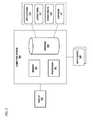
- FIG. 1illustrates a radial pattern graph, according to an exemplary embodiment
- FIG. 2illustrates a signal detection process flow chart, according to an exemplary embodiment
- FIG. 3schematically illustrates a computer system for performing signal detection methodology, in accordance with an exemplary embodiment.
- FIG. 1illustrates a graph representing an example of a radial pattern of several processes, each process having its own electronic signature.
- the x-axis of the graph in FIG. 1is a radius of an inspecting wafer, and the y-axis is any given measurement of a concerned process, including thickness or overlay vector or depth represented in measurement units such as Angstroms ( ⁇ ), nm, micrometers ( ⁇ m), etc. Wafer level data points are collected during each process and compiled for a radial signature build up. A shift in a radial pattern will cause more damage to the end product than a slight shift in the mean.
- each of the horizontal lines 101 , 103 , 105 , and 107represents a separate process having its own electronic signature.
- Lines 101 , 103 , 105 , and 107 and their corresponding wafer level data pointswould be represented in different colors on a display device associated with a processor.
- the hardware for calculating and graphically displaying a radial graphis explained below with reference to FIG. 3 .
- FIG. 2illustrates a process flow in accordance with an exemplary embodiment.
- wafer level datais collected in the form of electrical signatures during simulated processing steps in the production of a semiconductor device.
- the semiconductor deviceis represented with a simulated high density mode.
- the collecting of wafer level data across the entre wafer surfaceincludes collecting critical dimension (CD), thickness, resistance (RS), overlay (OVL) and optical critical dimension (OCD) data with metrology systems.
- CDcritical dimension
- RSresistance
- OTDoptical critical dimension
- hundreds and thousands of measurementscan be collected by way of metrology equipment to provide a dense measurement. It is an objective to monitor and collect this data during each process of semiconductor manufacturing.
- the final electrical properties of the end productcan be evaluated since the electrical properties have a certain electronic signature that can be compared to predetermined signatures.
- the wafer level datais collected and used with 3 rd order modeling or higher.
- 3 rd order model of a Zernike polynomialthe amount of signature can be monitored in detail.
- residualscan be calculated using the following equation:
- the residual and shape parameterscan be used as control signals.
- Step 203the electrical signatures from Step 201 are converted during each of the processing steps into signal matrix (MS) modeling parameters.
- the signalmust be maintained in order to be compensated.
- Step 205hardware, such as a programmed processor, compares the MS modeling parameters to predefined inline MS modeling parameters. It is an objective to control the shape of distribution of the MS modeling parameters.
- an early warning signalcan be generated when a defective MS modeling parameter is detected (Step 207 ). This early warning signal can improve process control by providing sufficient warning in order for the processor or technician to make the necessary adjustments to semiconductor manufacturing equipment.
- at least one processing stepcan be adjusted based on a result of the comparing step to improve process control. As a result of this adjustment, the wafer level data is optimized to improve leakage and performance of the semiconductor device end product (Step 211 ).
- Computer system 300includes at least one processor 301 , at least one memory 303 , and at least one storage 305 .
- the memory 303may, for instance, include dynamic storage, static storage, or a combination thereof.
- Computer system 300may be coupled to display 307 and one or more input devices 309 , such as a keyboard and a pointing device.
- Display 307may be utilized to provide one or more GUI interfaces.
- the computer system 300is equipped with a graphics card.
- Input devices 309may be utilized by users of computer system 300 to interact with, for instance, the GUI interfaces.
- Storage 305may store applications 311 , layout data (or information) 313 , mask design rules 315 , and at least one mask pattern database (or repository) 317 .
- Applications 311may include instructions (or computer program code) that when executed by processor 301 cause computer system 300 to perform one or more processes, such as one or more of the processes described herein.
- applications 311may include one or more signature detection tools and modeling tools.
- processor 301executing one or more sequences of one or more processor instructions contained in memory 303 .
- Such instructionsalso called computer instructions, software and program code, may be read into memory 303 from another computer-readable medium such as a storage device or a network link.
- Execution of the sequences of instructions contained in memory 303causes processor 301 to perform one or more of the method steps described herein.
- hardwaresuch as application-specific integrated circuits (ASICs)
- ASICsapplication-specific integrated circuits
- the embodiments of the present disclosurecan achieve several technical effects including the ability to provide a clear shape of process signature tracking by using several parameters and residuals.
- the present disclosureenjoys industrial applicability in any of various industrial applications, e.g., microprocessors, smart phones, mobile phones, cellular handsets, set-top boxes, DVD recorders and players, automotive navigation, printers and peripherals, networking and telecom equipment, gaming systems, and digital cameras.
- the present disclosuretherefore enjoys industrial applicability in any of various types of highly integrated semiconductor devices, particularly for 32 nm technology nodes and beyond.
Landscapes
- Engineering & Computer Science (AREA)
- Manufacturing & Machinery (AREA)
- Computer Hardware Design (AREA)
- Physics & Mathematics (AREA)
- General Physics & Mathematics (AREA)
- Microelectronics & Electronic Packaging (AREA)
- Theoretical Computer Science (AREA)
- Power Engineering (AREA)
- Human Computer Interaction (AREA)
- Automation & Control Theory (AREA)
- Evolutionary Computation (AREA)
- Geometry (AREA)
- General Engineering & Computer Science (AREA)
- Condensed Matter Physics & Semiconductors (AREA)
- Testing Or Measuring Of Semiconductors Or The Like (AREA)
Abstract
Description
- The present disclosure relates to a method and device for utilizing signal detection technology for fabrication (FAB) control. In particular, the present disclosure relates to signal detection technology for semiconductor devices in the 32 nanometer (nm) technology node and beyond.
- Signal detection methodology has been used in overlay misalignment modeling for semiconductor devices and for lens aberration analysis. Full scale wafer measurement has been previously performed and the measurements have been converted to specific parameters and residuals. In other areas, measurement and simulation techniques are used for wafer stress modeling analysis in semiconductor devices.
- With semiconductor yield control, every process of semiconductor manufacturing has its own electronic signature. These electronic signatures need to be maintained with sampled measurement, and most of the time the variation in one process can be compensated by other subsequent processes. However, the electronic signature can not be properly maintained with conventional methods.
- A need therefore exists for methodology and an apparatus for quantifying and monitoring wafer profile signatures during each process of semiconductor manufacturing.
- One aspect of the present disclosure is a method and apparatus for simulating individual process steps and producing parameters representing each individual process signal profile. Another aspect includes optimizing multiple processes within a wafer profile to obtain the optimum leakage and performance for a semiconductor device end product. Another aspect includes creating an electronic signature for each process step to generate a signal matrix (MS), or standard signature, which can serve as an early warning signal for FAB control.
- Additional aspects and other features of the present disclosure will be set forth in the description which follows and in part will be apparent to those having ordinary skill in the art upon examination of the following or may be learned from the practice of the present disclosure. The advantages of the present disclosure may be realized and obtained as particularly pointed out in the appended claims.
- According to the present disclosure, some technical effects may be achieved in part by a method including: collecting, by way of a programmed processor, wafer level data in the form of electrical signatures during processing steps in the production of a semiconductor device; converting the electrical signatures during each of the processing steps into MS modeling parameters; comparing the MS modeling parameters to predefined MS modeling parameters; and adjusting at least one processing step based on a result of the comparing step for process control.
- Aspects of the present disclosure include collecting the wafer level data during simulated processing steps in the production of the semiconductor device. Some aspects include the semiconductor device being represented with a simulated high density model. Other aspects include collecting critical dimension (CD), thickness, resistance (RS), overlay (OVL) and optical critical dimension (OCD) data with metrology systems. Certain aspects include collecting the wafer level data using 3rdorder modeling or higher. Further aspects include adjusting settings of processing equipment used in the actual production of the semiconductor device. Yet further aspects include collecting wafer level data across the wafer during the processing steps. Other aspects include optimizing the wafer level data to improve leakage of a semiconductor device end product. Additional aspects include optimizing the wafer level data to improve performance of a semiconductor device end product. Further aspects include generating an early warning signal prior to the adjusting step. Still further aspects include maintaining the electrical signatures for compensation purposes. Aspects additionally include controlling shape of distribution of MS modeling parameters.
- Another aspect of the present disclosure is a device a simulator for generating a high density model of a semiconductor device during its processing; and a processor configured to: collect wafer level data in the form of electrical signatures during processing steps in the production of the semiconductor device; convert the electrical signatures during each of the processing steps into MS modeling parameters; compare the MS modeling parameters to predefined MS modeling parameters; and adjust at least one processing step based on a result of the comparing step for process control.
- Aspects of the present disclosure include the processor being configured to collect CD, thickness, RS, OVL and OCD data with metrology systems. Other aspects include the processor being configured to collect the wafer level data with 3rdorder modeling or higher. Yet further aspects include the processor being configured to adjust one or more settings of processing equipment used in the actual production of the semiconductor device. Additional aspects include the processor being configured to generate an early warning signal prior to adjusting the one or more settings of processing equipment. Some aspects include the processor being configured to collect wafer level data across the wafer during the processing steps. Other aspects include the processor the processor being configured to optimize the wafer level data to improve leakage and performance of a semiconductor device end product.
- Yet another aspect of the present disclosure is a method including collecting, by way of a programmed processor, wafer level data in the form of electrical signatures during simulated processing steps in the production of a semiconductor device; converting the electrical signatures during each of the processing steps into MS modeling parameters; comparing the MS modeling parameters to predefined MS modeling parameters; generating an early warning signal when a defective MS modeling parameter is detected; and adjusting at least one processing step based on a result of the comparing step for process control.
- Aspects of the present disclosure include optimizing the wafer level data to improve leakage and performance of the semiconductor device end product.
- Additional aspects and technical effects of the present disclosure will become readily apparent to those skilled in the art from the following detailed description wherein embodiments of the present disclosure are described simply by way of illustration of the best mode contemplated to carry out the present disclosure. As will be realized, the present disclosure is capable of other and different embodiments, and its several details are capable of modifications in various obvious respects, all without departing from the present disclosure. Accordingly, the drawings and description are to be regarded as illustrative in nature, and not as restrictive.
- The present disclosure is illustrated by way of example, and not by way of limitation, in the figures of the accompanying drawing and in which like reference numerals refer to similar elements and in which:
FIG. 1 illustrates a radial pattern graph, according to an exemplary embodiment;FIG. 2 illustrates a signal detection process flow chart, according to an exemplary embodiment;FIG. 3 schematically illustrates a computer system for performing signal detection methodology, in accordance with an exemplary embodiment.- In the following description, for the purposes of explanation, numerous specific details are set forth in order to provide a thorough understanding of exemplary embodiments. It should be apparent, however, that exemplary embodiments may be practiced without these specific details or with an equivalent arrangement. In other instances, well-known structures and devices are shown in block diagram form in order to avoid unnecessarily obscuring exemplary embodiments. In addition, unless otherwise indicated, all numbers expressing quantities, ratios, and numerical properties of ingredients, reaction conditions, and so forth used in the specification and claims are to be understood as being modified in all instances by the term “about.”
FIG. 1 illustrates a graph representing an example of a radial pattern of several processes, each process having its own electronic signature. The x-axis of the graph inFIG. 1 is a radius of an inspecting wafer, and the y-axis is any given measurement of a concerned process, including thickness or overlay vector or depth represented in measurement units such as Angstroms (Å), nm, micrometers (μm), etc. Wafer level data points are collected during each process and compiled for a radial signature build up. A shift in a radial pattern will cause more damage to the end product than a slight shift in the mean. In the graph ofFIG. 1 , each of thehorizontal lines Lines FIG. 3 .FIG. 2 illustrates a process flow in accordance with an exemplary embodiment. InStep 201, wafer level data is collected in the form of electrical signatures during simulated processing steps in the production of a semiconductor device. The semiconductor device is represented with a simulated high density mode. The collecting of wafer level data across the entre wafer surface includes collecting critical dimension (CD), thickness, resistance (RS), overlay (OVL) and optical critical dimension (OCD) data with metrology systems. In certain examples, hundreds and thousands of measurements can be collected by way of metrology equipment to provide a dense measurement. It is an objective to monitor and collect this data during each process of semiconductor manufacturing. The final electrical properties of the end product can be evaluated since the electrical properties have a certain electronic signature that can be compared to predetermined signatures.- The wafer level data is collected and used with 3rdorder modeling or higher. In certain embodiments, by using 3rdorder model of a Zernike polynomial, the amount of signature can be monitored in detail. Moreover, with 3rdorder modeling (or higher), residuals can be calculated using the following equation:
Σsite0all siteFx−each number=residual- The residual and shape parameters can be used as control signals.
- In
Step 203, the electrical signatures fromStep 201 are converted during each of the processing steps into signal matrix (MS) modeling parameters. The signal must be maintained in order to be compensated. InStep 205, hardware, such as a programmed processor, compares the MS modeling parameters to predefined inline MS modeling parameters. It is an objective to control the shape of distribution of the MS modeling parameters. In accordance with exemplary embodiments, an early warning signal can be generated when a defective MS modeling parameter is detected (Step207). This early warning signal can improve process control by providing sufficient warning in order for the processor or technician to make the necessary adjustments to semiconductor manufacturing equipment. InStep 209, at least one processing step can be adjusted based on a result of the comparing step to improve process control. As a result of this adjustment, the wafer level data is optimized to improve leakage and performance of the semiconductor device end product (Step211). - The processes described herein may be implemented via software, hardware, firmware, or a combination thereof. Exemplary hardware (e.g., computing hardware) is schematically illustrated in
FIG. 3 . As shown,computer system 300 includes at least oneprocessor 301, at least onememory 303, and at least onestorage 305. Thememory 303 may, for instance, include dynamic storage, static storage, or a combination thereof.Computer system 300 may be coupled todisplay 307 and one ormore input devices 309, such as a keyboard and a pointing device.Display 307 may be utilized to provide one or more GUI interfaces. Thecomputer system 300 is equipped with a graphics card.Input devices 309 may be utilized by users ofcomputer system 300 to interact with, for instance, the GUI interfaces.Storage 305 may storeapplications 311, layout data (or information)313,mask design rules 315, and at least one mask pattern database (or repository)317.Applications 311 may include instructions (or computer program code) that when executed byprocessor 301cause computer system 300 to perform one or more processes, such as one or more of the processes described herein. In exemplary embodiments,applications 311 may include one or more signature detection tools and modeling tools. - It is noted that, in various aspects, some or all of the techniques described herein are performed by
computer system 300 in response toprocessor 301 executing one or more sequences of one or more processor instructions contained inmemory 303. Such instructions, also called computer instructions, software and program code, may be read intomemory 303 from another computer-readable medium such as a storage device or a network link. Execution of the sequences of instructions contained inmemory 303 causesprocessor 301 to perform one or more of the method steps described herein. In alternative embodiments, hardware, such as application-specific integrated circuits (ASICs), may be used in place of or in combination with modeling software to implement the invention. Thus, embodiments of the invention are not limited to any specific combination of hardware and software, unless otherwise explicitly stated herein. - The embodiments of the present disclosure can achieve several technical effects including the ability to provide a clear shape of process signature tracking by using several parameters and residuals. The present disclosure enjoys industrial applicability in any of various industrial applications, e.g., microprocessors, smart phones, mobile phones, cellular handsets, set-top boxes, DVD recorders and players, automotive navigation, printers and peripherals, networking and telecom equipment, gaming systems, and digital cameras. The present disclosure therefore enjoys industrial applicability in any of various types of highly integrated semiconductor devices, particularly for 32 nm technology nodes and beyond.
- In the preceding description, the present disclosure is described with reference to specifically exemplary embodiments thereof. It will, however, be evident that various modifications and changes may be made thereto without departing from the broader spirit and scope of the present disclosure, as set forth in the claims. The specification and drawings are, accordingly, to be regarded as illustrative and not as restrictive. It is understood that the present disclosure is capable of using various other combinations and embodiments and is capable of any changes or modifications within the scope of the inventive concept as expressed herein.
Claims (21)
Priority Applications (3)
| Application Number | Priority Date | Filing Date | Title |
|---|---|---|---|
| US14/993,320US20170199511A1 (en) | 2016-01-12 | 2016-01-12 | Signal detection metholodogy for fabrication control |
| CN201710019660.8ACN107066668A (en) | 2016-01-12 | 2017-01-11 | Signal detecting method for manufacturing control |
| TW106100993ATW201736999A (en) | 2016-01-12 | 2017-01-12 | Signal detection method for manufacturing control |
Applications Claiming Priority (1)
| Application Number | Priority Date | Filing Date | Title |
|---|---|---|---|
| US14/993,320US20170199511A1 (en) | 2016-01-12 | 2016-01-12 | Signal detection metholodogy for fabrication control |
Publications (1)
| Publication Number | Publication Date |
|---|---|
| US20170199511A1true US20170199511A1 (en) | 2017-07-13 |
Family
ID=59275698
Family Applications (1)
| Application Number | Title | Priority Date | Filing Date |
|---|---|---|---|
| US14/993,320AbandonedUS20170199511A1 (en) | 2016-01-12 | 2016-01-12 | Signal detection metholodogy for fabrication control |
Country Status (3)
| Country | Link |
|---|---|
| US (1) | US20170199511A1 (en) |
| CN (1) | CN107066668A (en) |
| TW (1) | TW201736999A (en) |
Citations (32)
| Publication number | Priority date | Publication date | Assignee | Title |
|---|---|---|---|---|
| US6036346A (en)* | 1996-05-20 | 2000-03-14 | Ricoh Company, Ltd. | Semiconductor manufacturing process simulation apparatus for calculating a pressure field generated by a dislocation loop |
| US6041270A (en)* | 1997-12-05 | 2000-03-21 | Advanced Micro Devices, Inc. | Automatic recipe adjust and download based on process control window |
| US20020077719A1 (en)* | 2000-12-18 | 2002-06-20 | Hao Howard G. | Variable parameter controls for semiconductor processes |
| US6608920B1 (en)* | 1998-10-29 | 2003-08-19 | Applied Materials, Inc. | Target acquisition technique for CD measurement machine |
| US20040137677A1 (en)* | 2002-11-28 | 2004-07-15 | Asml Netherlands B.V. | Device manufacturing method and computer program |
| US20040181768A1 (en)* | 2003-03-12 | 2004-09-16 | Krukar Richard H. | Model pattern simulation of semiconductor wafer processing steps |
| US20050235246A1 (en)* | 2002-06-07 | 2005-10-20 | Praesagus, Inc., A Massachusetts Corporation | Use of models in integrated circuit fabrication |
| US7003758B2 (en)* | 2003-10-07 | 2006-02-21 | Brion Technologies, Inc. | System and method for lithography simulation |
| US7151976B2 (en)* | 2004-09-17 | 2006-12-19 | Mks Instruments, Inc. | Multivariate control of semiconductor processes |
| US20070061773A1 (en)* | 2005-09-09 | 2007-03-15 | Brion Technologies, Inc. | Method for selecting and optimizing exposure tool using an individual mask error model |
| US20090066784A1 (en)* | 2007-09-05 | 2009-03-12 | Sony Corporation | Image processing apparatus and method |
| US20090144691A1 (en)* | 2007-11-29 | 2009-06-04 | Tokyo Electron Limited | Enhanced Process Yield Using a Hot-Spot Library |
| US20100114553A1 (en)* | 2008-10-30 | 2010-05-06 | Kyung Rok Kim | Systems and Methods for Executing Unified Process-Device-Circuit Simulation |
| US20110053381A1 (en)* | 2008-02-08 | 2011-03-03 | Tokyo Electron Limited | Method for modifying insulating film with plasma |
| US20110112678A1 (en)* | 2009-11-11 | 2011-05-12 | Taiwan Semiconductor Manufacturing Company, Ltd. | Advanced process control for new tapeout product |
| US20110124193A1 (en)* | 2009-11-25 | 2011-05-26 | Taiwan Semiconductor Manufacturing Company, Ltd. | Customized patterning modulation and optimization |
| US20110153055A1 (en)* | 2009-12-17 | 2011-06-23 | Taiwan Semiconductor Manufacturing Co., Ltd. | Wide-range quick tunable transistor model |
| US20110177458A1 (en)* | 2010-01-15 | 2011-07-21 | Toshiya Kotani | Exposure determining method, method of manufacturing semiconductor device, and computer program product |
| US20110207247A1 (en)* | 2010-02-19 | 2011-08-25 | Chan Hwang | Method of correcting overlay and semiconductor device manufacturing method using the same |
| US20120117522A1 (en)* | 2010-11-10 | 2012-05-10 | Asml Netherlands B.V. | Optimization of Source, Mask and Projection Optics |
| US20130212543A1 (en)* | 2012-02-09 | 2013-08-15 | Asml Netherlands B.V. | Lens heating aware source mask optimization for advanced lithography |
| US8560978B2 (en)* | 2010-11-10 | 2013-10-15 | Asml Netherlands B.V. | Pattern-dependent proximity matching/tuning including light manipulation by projection optics |
| US20130330843A1 (en)* | 2012-06-07 | 2013-12-12 | Globalfoundries Inc. | Method of manufacturing scaled equivalent oxide thickness gate stacks in semiconductor devices and related design structure |
| US20140107998A1 (en)* | 2012-10-11 | 2014-04-17 | Kla-Tencor Corporation | System and Method to Emulate Finite Element Model Based Prediction of In-Plane Distortions Due to Semiconductor Wafer Chucking |
| US20140114597A1 (en)* | 2012-10-19 | 2014-04-24 | Kla-Tencor Corporation | Systems, Methods and Metrics for Wafer High Order Shape Characterization and Wafer Classification Using Wafer Dimensional Geometry Tool |
| US20150060861A1 (en)* | 2013-09-03 | 2015-03-05 | Taiwan Semiconductor Manufacturing Co., Ltd. | GaN Misfets with Hybrid AI203 As Gate Dielectric |
| US20150120216A1 (en)* | 2013-10-29 | 2015-04-30 | Kla-Tencor Corporation | Process-Induced Distortion Prediction and Feedforward and Feedback Correction of Overlay Errors |
| US20150211122A1 (en)* | 2009-02-13 | 2015-07-30 | Taiwan Semiconductor Manufacturing Co., Ltd. | Multi-zone temperature control for semiconductor wafer |
| US9188974B1 (en)* | 2004-02-13 | 2015-11-17 | Kla-Tencor Technologies Corp. | Methods for improved monitor and control of lithography processes |
| US20160240650A1 (en)* | 2015-02-13 | 2016-08-18 | Taiwan Semiconductor Manufacturing Co., Ltd | Semiconductor structure with extending gate structure and method for forming the same |
| US20160371423A1 (en)* | 2015-06-22 | 2016-12-22 | Kla-Tencor Corporation | Process-Induced Asymmetry Detection, Quantification, and Control Using Patterned Wafer Geometry Measurements |
| US20170132352A1 (en)* | 2015-11-09 | 2017-05-11 | Applied Materials, Inc. | Wafer point by point analysis and data presentation |
Family Cites Families (2)
| Publication number | Priority date | Publication date | Assignee | Title |
|---|---|---|---|---|
| US8185230B2 (en)* | 2002-08-22 | 2012-05-22 | Advanced Micro Devices, Inc. | Method and apparatus for predicting device electrical parameters during fabrication |
| CN102637215A (en)* | 2011-02-10 | 2012-08-15 | 上海宏力半导体制造有限公司 | Modeling method of semiconductor device |
- 2016
- 2016-01-12USUS14/993,320patent/US20170199511A1/ennot_activeAbandoned
- 2017
- 2017-01-11CNCN201710019660.8Apatent/CN107066668A/enactivePending
- 2017-01-12TWTW106100993Apatent/TW201736999A/enunknown
Patent Citations (32)
| Publication number | Priority date | Publication date | Assignee | Title |
|---|---|---|---|---|
| US6036346A (en)* | 1996-05-20 | 2000-03-14 | Ricoh Company, Ltd. | Semiconductor manufacturing process simulation apparatus for calculating a pressure field generated by a dislocation loop |
| US6041270A (en)* | 1997-12-05 | 2000-03-21 | Advanced Micro Devices, Inc. | Automatic recipe adjust and download based on process control window |
| US6608920B1 (en)* | 1998-10-29 | 2003-08-19 | Applied Materials, Inc. | Target acquisition technique for CD measurement machine |
| US20020077719A1 (en)* | 2000-12-18 | 2002-06-20 | Hao Howard G. | Variable parameter controls for semiconductor processes |
| US20050235246A1 (en)* | 2002-06-07 | 2005-10-20 | Praesagus, Inc., A Massachusetts Corporation | Use of models in integrated circuit fabrication |
| US20040137677A1 (en)* | 2002-11-28 | 2004-07-15 | Asml Netherlands B.V. | Device manufacturing method and computer program |
| US20040181768A1 (en)* | 2003-03-12 | 2004-09-16 | Krukar Richard H. | Model pattern simulation of semiconductor wafer processing steps |
| US7003758B2 (en)* | 2003-10-07 | 2006-02-21 | Brion Technologies, Inc. | System and method for lithography simulation |
| US9188974B1 (en)* | 2004-02-13 | 2015-11-17 | Kla-Tencor Technologies Corp. | Methods for improved monitor and control of lithography processes |
| US7151976B2 (en)* | 2004-09-17 | 2006-12-19 | Mks Instruments, Inc. | Multivariate control of semiconductor processes |
| US20070061773A1 (en)* | 2005-09-09 | 2007-03-15 | Brion Technologies, Inc. | Method for selecting and optimizing exposure tool using an individual mask error model |
| US20090066784A1 (en)* | 2007-09-05 | 2009-03-12 | Sony Corporation | Image processing apparatus and method |
| US20090144691A1 (en)* | 2007-11-29 | 2009-06-04 | Tokyo Electron Limited | Enhanced Process Yield Using a Hot-Spot Library |
| US20110053381A1 (en)* | 2008-02-08 | 2011-03-03 | Tokyo Electron Limited | Method for modifying insulating film with plasma |
| US20100114553A1 (en)* | 2008-10-30 | 2010-05-06 | Kyung Rok Kim | Systems and Methods for Executing Unified Process-Device-Circuit Simulation |
| US20150211122A1 (en)* | 2009-02-13 | 2015-07-30 | Taiwan Semiconductor Manufacturing Co., Ltd. | Multi-zone temperature control for semiconductor wafer |
| US20110112678A1 (en)* | 2009-11-11 | 2011-05-12 | Taiwan Semiconductor Manufacturing Company, Ltd. | Advanced process control for new tapeout product |
| US20110124193A1 (en)* | 2009-11-25 | 2011-05-26 | Taiwan Semiconductor Manufacturing Company, Ltd. | Customized patterning modulation and optimization |
| US20110153055A1 (en)* | 2009-12-17 | 2011-06-23 | Taiwan Semiconductor Manufacturing Co., Ltd. | Wide-range quick tunable transistor model |
| US20110177458A1 (en)* | 2010-01-15 | 2011-07-21 | Toshiya Kotani | Exposure determining method, method of manufacturing semiconductor device, and computer program product |
| US20110207247A1 (en)* | 2010-02-19 | 2011-08-25 | Chan Hwang | Method of correcting overlay and semiconductor device manufacturing method using the same |
| US8560978B2 (en)* | 2010-11-10 | 2013-10-15 | Asml Netherlands B.V. | Pattern-dependent proximity matching/tuning including light manipulation by projection optics |
| US20120117522A1 (en)* | 2010-11-10 | 2012-05-10 | Asml Netherlands B.V. | Optimization of Source, Mask and Projection Optics |
| US20130212543A1 (en)* | 2012-02-09 | 2013-08-15 | Asml Netherlands B.V. | Lens heating aware source mask optimization for advanced lithography |
| US20130330843A1 (en)* | 2012-06-07 | 2013-12-12 | Globalfoundries Inc. | Method of manufacturing scaled equivalent oxide thickness gate stacks in semiconductor devices and related design structure |
| US20140107998A1 (en)* | 2012-10-11 | 2014-04-17 | Kla-Tencor Corporation | System and Method to Emulate Finite Element Model Based Prediction of In-Plane Distortions Due to Semiconductor Wafer Chucking |
| US20140114597A1 (en)* | 2012-10-19 | 2014-04-24 | Kla-Tencor Corporation | Systems, Methods and Metrics for Wafer High Order Shape Characterization and Wafer Classification Using Wafer Dimensional Geometry Tool |
| US20150060861A1 (en)* | 2013-09-03 | 2015-03-05 | Taiwan Semiconductor Manufacturing Co., Ltd. | GaN Misfets with Hybrid AI203 As Gate Dielectric |
| US20150120216A1 (en)* | 2013-10-29 | 2015-04-30 | Kla-Tencor Corporation | Process-Induced Distortion Prediction and Feedforward and Feedback Correction of Overlay Errors |
| US20160240650A1 (en)* | 2015-02-13 | 2016-08-18 | Taiwan Semiconductor Manufacturing Co., Ltd | Semiconductor structure with extending gate structure and method for forming the same |
| US20160371423A1 (en)* | 2015-06-22 | 2016-12-22 | Kla-Tencor Corporation | Process-Induced Asymmetry Detection, Quantification, and Control Using Patterned Wafer Geometry Measurements |
| US20170132352A1 (en)* | 2015-11-09 | 2017-05-11 | Applied Materials, Inc. | Wafer point by point analysis and data presentation |
Non-Patent Citations (2)
| Title |
|---|
| Ju et al, "Application Of Overlay Modeling And Control With Zernike Polynomials In An HVM Environment" March 18, 2016, pages 6* |
| Veeraraghaven et al, "Simulation of Non-Uniform Wafer Geometry and Thin Film Residual Stress on Overlay Errors", 2011, pages 1-6.* |
Also Published As
| Publication number | Publication date |
|---|---|
| CN107066668A (en) | 2017-08-18 |
| TW201736999A (en) | 2017-10-16 |
Similar Documents
| Publication | Publication Date | Title |
|---|---|---|
| US10657638B2 (en) | Wafer map pattern detection based on supervised machine learning | |
| TWI808815B (en) | System and method of semiconductor fabrication process control and computer program product | |
| KR102568074B1 (en) | Systems and methods for predicting defects and critical dimensions using deep learning in semiconductor manufacturing processes | |
| US11150562B2 (en) | Optimizing an apparatus for multi-stage processing of product units | |
| US9097978B2 (en) | Method and apparatus to characterize photolithography lens quality | |
| KR20190139967A (en) | Method of predicting the yield of the device manufacturing process | |
| JP2011513993A (en) | Process control using process data and production volume data | |
| JP2019215501A5 (en) | ||
| Fan et al. | Fault diagnosis of wafer acceptance test and chip probing between front-end-of-line and back-end-of-line processes | |
| Dong et al. | Wafer yield prediction using derived spatial variables | |
| Xu et al. | A fast ramp-up framework for wafer yield improvement in semiconductor manufacturing systems | |
| US7533313B1 (en) | Method and apparatus for identifying outlier data | |
| Tabery et al. | SEM image contouring for OPC model calibration and verification | |
| JP2011054804A (en) | Method and system for management of semiconductor manufacturing device | |
| Mishanov et al. | Forecasting models generation of the electronic means quality | |
| US20170199511A1 (en) | Signal detection metholodogy for fabrication control | |
| Saib et al. | Multivariate analysis methodology for the study of massive multidimensional SEM data | |
| JP5374727B2 (en) | Lithography simulation apparatus, lithography simulation program, and semiconductor device design and manufacturing method using the same | |
| van Dijk et al. | Smart implant-layer overlay metrology to enable fab cycle time reduction | |
| CN105892223A (en) | Method for optimizing optical proximity effect (OPC) verification | |
| US20130325395A1 (en) | Co-optimization of scatterometry mark design and process monitor mark design | |
| KR20240124300A (en) | Technique for identifying outlier modules from a reference population for machine diagnostics | |
| CN109857881B (en) | Quantitative analysis method of verification graph for OPC verification | |
| Groeger et al. | Optimizing focus and dose process windows for robust process control using a multi-feature analysis | |
| US10699971B2 (en) | Method for processing of a further layer on a semiconductor wafer |
Legal Events
| Date | Code | Title | Description |
|---|---|---|---|
| AS | Assignment | Owner name:GLOBALFOUNDRIES INC., CAYMAN ISLANDS Free format text:ASSIGNMENT OF ASSIGNORS INTEREST;ASSIGNORS:PARK, DONGSUK;VAID, ALOK;NAIR, BINOD KUMAR GOPALAKRISHNAN;REEL/FRAME:037464/0259 Effective date:20151231 | |
| AS | Assignment | Owner name:WILMINGTON TRUST, NATIONAL ASSOCIATION, DELAWARE Free format text:SECURITY AGREEMENT;ASSIGNOR:GLOBALFOUNDRIES INC.;REEL/FRAME:049490/0001 Effective date:20181127 | |
| STCB | Information on status: application discontinuation | Free format text:ABANDONED -- FAILURE TO RESPOND TO AN OFFICE ACTION | |
| AS | Assignment | Owner name:GLOBALFOUNDRIES INC., CAYMAN ISLANDS Free format text:RELEASE BY SECURED PARTY;ASSIGNOR:WILMINGTON TRUST, NATIONAL ASSOCIATION;REEL/FRAME:054636/0001 Effective date:20201117 | |
| AS | Assignment | Owner name:GLOBALFOUNDRIES U.S. INC., NEW YORK Free format text:RELEASE BY SECURED PARTY;ASSIGNOR:WILMINGTON TRUST, NATIONAL ASSOCIATION;REEL/FRAME:056987/0001 Effective date:20201117 |