US20170178939A1 - Substrate transport device and substrate processing apparatus - Google Patents
Substrate transport device and substrate processing apparatusDownload PDFInfo
- Publication number
- US20170178939A1 US20170178939A1US14/973,359US201514973359AUS2017178939A1US 20170178939 A1US20170178939 A1US 20170178939A1US 201514973359 AUS201514973359 AUS 201514973359AUS 2017178939 A1US2017178939 A1US 2017178939A1
- Authority
- US
- United States
- Prior art keywords
- shaft
- transport device
- rotation arm
- substrate
- substrate transport
- Prior art date
- Legal status (The legal status is an assumption and is not a legal conclusion. Google has not performed a legal analysis and makes no representation as to the accuracy of the status listed.)
- Granted
Links
- 239000000758substrateSubstances0.000titleclaimsabstractdescription154
- 238000000034methodMethods0.000claimsdescription14
- 230000002093peripheral effectEffects0.000claimsdescription5
- 230000002829reductive effectEffects0.000claimsdescription2
- 230000033001locomotionEffects0.000description5
- 239000010408filmSubstances0.000description4
- 238000012986modificationMethods0.000description3
- 230000004048modificationEffects0.000description3
- 239000007789gasSubstances0.000description2
- 230000000670limiting effectEffects0.000description2
- 235000012431wafersNutrition0.000description2
- 210000000436anusAnatomy0.000description1
- 238000005452bendingMethods0.000description1
- 239000000919ceramicSubstances0.000description1
- 239000007795chemical reaction productSubstances0.000description1
- 238000010276constructionMethods0.000description1
- 230000003247decreasing effectEffects0.000description1
- 239000000428dustSubstances0.000description1
- 230000002401inhibitory effectEffects0.000description1
- 239000002245particleSubstances0.000description1
- 230000001360synchronised effectEffects0.000description1
- 239000010409thin filmSubstances0.000description1
Images


Classifications
- H—ELECTRICITY
- H01—ELECTRIC ELEMENTS
- H01L—SEMICONDUCTOR DEVICES NOT COVERED BY CLASS H10
- H01L21/00—Processes or apparatus adapted for the manufacture or treatment of semiconductor or solid state devices or of parts thereof
- H01L21/67—Apparatus specially adapted for handling semiconductor or electric solid state devices during manufacture or treatment thereof; Apparatus specially adapted for handling wafers during manufacture or treatment of semiconductor or electric solid state devices or components ; Apparatus not specifically provided for elsewhere
- H01L21/677—Apparatus specially adapted for handling semiconductor or electric solid state devices during manufacture or treatment thereof; Apparatus specially adapted for handling wafers during manufacture or treatment of semiconductor or electric solid state devices or components ; Apparatus not specifically provided for elsewhere for conveying, e.g. between different workstations
- H01L21/67739—Apparatus specially adapted for handling semiconductor or electric solid state devices during manufacture or treatment thereof; Apparatus specially adapted for handling wafers during manufacture or treatment of semiconductor or electric solid state devices or components ; Apparatus not specifically provided for elsewhere for conveying, e.g. between different workstations into and out of processing chamber
- H01L21/67742—Mechanical parts of transfer devices
- H—ELECTRICITY
- H01—ELECTRIC ELEMENTS
- H01L—SEMICONDUCTOR DEVICES NOT COVERED BY CLASS H10
- H01L21/00—Processes or apparatus adapted for the manufacture or treatment of semiconductor or solid state devices or of parts thereof
- H01L21/67—Apparatus specially adapted for handling semiconductor or electric solid state devices during manufacture or treatment thereof; Apparatus specially adapted for handling wafers during manufacture or treatment of semiconductor or electric solid state devices or components ; Apparatus not specifically provided for elsewhere
- H01L21/67005—Apparatus not specifically provided for elsewhere
- H01L21/67011—Apparatus for manufacture or treatment
- H01L21/67155—Apparatus for manufacturing or treating in a plurality of work-stations
- H01L21/6719—Apparatus for manufacturing or treating in a plurality of work-stations characterized by the construction of the processing chambers, e.g. modular processing chambers
- H—ELECTRICITY
- H01—ELECTRIC ELEMENTS
- H01L—SEMICONDUCTOR DEVICES NOT COVERED BY CLASS H10
- H01L21/00—Processes or apparatus adapted for the manufacture or treatment of semiconductor or solid state devices or of parts thereof
- H01L21/67—Apparatus specially adapted for handling semiconductor or electric solid state devices during manufacture or treatment thereof; Apparatus specially adapted for handling wafers during manufacture or treatment of semiconductor or electric solid state devices or components ; Apparatus not specifically provided for elsewhere
- H01L21/683—Apparatus specially adapted for handling semiconductor or electric solid state devices during manufacture or treatment thereof; Apparatus specially adapted for handling wafers during manufacture or treatment of semiconductor or electric solid state devices or components ; Apparatus not specifically provided for elsewhere for supporting or gripping
- H01L21/687—Apparatus specially adapted for handling semiconductor or electric solid state devices during manufacture or treatment thereof; Apparatus specially adapted for handling wafers during manufacture or treatment of semiconductor or electric solid state devices or components ; Apparatus not specifically provided for elsewhere for supporting or gripping using mechanical means, e.g. chucks, clamps or pinches
- H01L21/68714—Apparatus specially adapted for handling semiconductor or electric solid state devices during manufacture or treatment thereof; Apparatus specially adapted for handling wafers during manufacture or treatment of semiconductor or electric solid state devices or components ; Apparatus not specifically provided for elsewhere for supporting or gripping using mechanical means, e.g. chucks, clamps or pinches the wafers being placed on a susceptor, stage or support
- H01L21/68764—Apparatus specially adapted for handling semiconductor or electric solid state devices during manufacture or treatment thereof; Apparatus specially adapted for handling wafers during manufacture or treatment of semiconductor or electric solid state devices or components ; Apparatus not specifically provided for elsewhere for supporting or gripping using mechanical means, e.g. chucks, clamps or pinches the wafers being placed on a susceptor, stage or support characterised by a movable susceptor, stage or support, others than those only rotating on their own vertical axis, e.g. susceptors on a rotating caroussel
- H—ELECTRICITY
- H01—ELECTRIC ELEMENTS
- H01L—SEMICONDUCTOR DEVICES NOT COVERED BY CLASS H10
- H01L21/00—Processes or apparatus adapted for the manufacture or treatment of semiconductor or solid state devices or of parts thereof
- H01L21/67—Apparatus specially adapted for handling semiconductor or electric solid state devices during manufacture or treatment thereof; Apparatus specially adapted for handling wafers during manufacture or treatment of semiconductor or electric solid state devices or components ; Apparatus not specifically provided for elsewhere
- H01L21/683—Apparatus specially adapted for handling semiconductor or electric solid state devices during manufacture or treatment thereof; Apparatus specially adapted for handling wafers during manufacture or treatment of semiconductor or electric solid state devices or components ; Apparatus not specifically provided for elsewhere for supporting or gripping
- H01L21/687—Apparatus specially adapted for handling semiconductor or electric solid state devices during manufacture or treatment thereof; Apparatus specially adapted for handling wafers during manufacture or treatment of semiconductor or electric solid state devices or components ; Apparatus not specifically provided for elsewhere for supporting or gripping using mechanical means, e.g. chucks, clamps or pinches
- H01L21/68714—Apparatus specially adapted for handling semiconductor or electric solid state devices during manufacture or treatment thereof; Apparatus specially adapted for handling wafers during manufacture or treatment of semiconductor or electric solid state devices or components ; Apparatus not specifically provided for elsewhere for supporting or gripping using mechanical means, e.g. chucks, clamps or pinches the wafers being placed on a susceptor, stage or support
- H01L21/68771—Apparatus specially adapted for handling semiconductor or electric solid state devices during manufacture or treatment thereof; Apparatus specially adapted for handling wafers during manufacture or treatment of semiconductor or electric solid state devices or components ; Apparatus not specifically provided for elsewhere for supporting or gripping using mechanical means, e.g. chucks, clamps or pinches the wafers being placed on a susceptor, stage or support characterised by supporting more than one semiconductor substrate
- H—ELECTRICITY
- H01—ELECTRIC ELEMENTS
- H01L—SEMICONDUCTOR DEVICES NOT COVERED BY CLASS H10
- H01L21/00—Processes or apparatus adapted for the manufacture or treatment of semiconductor or solid state devices or of parts thereof
- H01L21/67—Apparatus specially adapted for handling semiconductor or electric solid state devices during manufacture or treatment thereof; Apparatus specially adapted for handling wafers during manufacture or treatment of semiconductor or electric solid state devices or components ; Apparatus not specifically provided for elsewhere
- H01L21/683—Apparatus specially adapted for handling semiconductor or electric solid state devices during manufacture or treatment thereof; Apparatus specially adapted for handling wafers during manufacture or treatment of semiconductor or electric solid state devices or components ; Apparatus not specifically provided for elsewhere for supporting or gripping
- H01L21/687—Apparatus specially adapted for handling semiconductor or electric solid state devices during manufacture or treatment thereof; Apparatus specially adapted for handling wafers during manufacture or treatment of semiconductor or electric solid state devices or components ; Apparatus not specifically provided for elsewhere for supporting or gripping using mechanical means, e.g. chucks, clamps or pinches
- H01L21/68714—Apparatus specially adapted for handling semiconductor or electric solid state devices during manufacture or treatment thereof; Apparatus specially adapted for handling wafers during manufacture or treatment of semiconductor or electric solid state devices or components ; Apparatus not specifically provided for elsewhere for supporting or gripping using mechanical means, e.g. chucks, clamps or pinches the wafers being placed on a susceptor, stage or support
- H01L21/68785—Apparatus specially adapted for handling semiconductor or electric solid state devices during manufacture or treatment thereof; Apparatus specially adapted for handling wafers during manufacture or treatment of semiconductor or electric solid state devices or components ; Apparatus not specifically provided for elsewhere for supporting or gripping using mechanical means, e.g. chucks, clamps or pinches the wafers being placed on a susceptor, stage or support characterised by the mechanical construction of the susceptor, stage or support
Definitions
- the present inventionrelates to a substrate transport device used to transport substrates, and to a substrate processing apparatus.
- US2009/324828discloses a film forming apparatus and technique in which at least two reactive gases are supplied one after another to a surface of a substrate; the cycle of supplying the reactive gases is executed a number of times; and a multiplicity of layers of a reaction product are thereby laid one on another to form a thin film.
- a transport armis used to move wafers.
- the armhas a fixed first end and a free second end, a peripheral portion of the arm at the second end is bent downward by the weight thereof. There is a possibility of the substrate sliding easily on the arm due to this bending.
- an object of the present inventionis to provide a substrate transport device and a substrate processing apparatus capable of preventing a substrate from moving on an arm during transport of the substrate.
- a substrate transport deviceincludes a shaft, a first moving part for moving the shaft in a vertical direction and in a rotational direction, at least one rotation arm attached to the shaft, and a supporting part having an upper surface waved as seen front view, wherein the rotation arm includes a contact rotation arm which directly or indirectly contacts the upper surface of the supporting part.
- a substrate processing apparatusincludes a substrate transport device having a shaft, a first moving part for moving the shaft in a vertical direction and in a rotational direction, at least one rotation arm attached to the shaft, and a supporting part having an upper surface waved as seen front view, wherein the rotation arm includes a contact rotation arm which directly or indirectly contacts the upper surface of the supporting part, and a plurality of process regions, wherein the substrate transport device moves a substrate between the plurality of process regions.
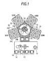
- FIG. 1is a plan view of a substrate processing apparatus including a substrate transport device according to a first embodiment
- FIG. 2is a perspective view of the substrate transport device
- FIG. 3is a development of the cylindrical supporting part
- FIG. 4is a plan view of the substrate transport device
- FIG. 5is a plan view of the substrate transport device
- FIG. 6is a sectional view of the substrate transport device
- FIG. 7is a plan view of the substrate transport device
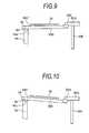
- FIG. 8is a sectional view of the substrate transport device
- FIG. 9is a sectional view of a portion of the substrate transport device according to the second embodiment.
- FIG. 10is a sectional view of a portion of the substrate transport device
- FIG. 11is a side view of the wheel.
- FIG. 12is a plan view of a rotation arm according to the third embodiment.
- a substrate transport device and a substrate processing apparatuswill be described with reference to the drawings. Components identical or corresponding to each other are indicated by the same reference characters and repeated description of them is avoided in some cases.
- FIG. 1is a plan view of a substrate processing apparatus including a substrate transport device according to a first embodiment of the present invention.
- This substrate processing apparatusis provided with a transport chamber 10 .
- the interior of the transport chamber 10is maintained generally at atmospheric pressure.
- the transport chamberis called an equipment front end module (EFEM).
- EFEMequipment front end module
- a robot arm 12 for transporting substratesis provided in the transport chamber 10 .
- This robot arm 12is called a Front End Robot (FERB).
- the robot arm 12includes, for example, an upper arm and a lower arm and is, therefore, capable of transporting two substrates separately.
- a load port 14is attached to a side of the transport chamber 10 .
- the load port 14is a table on which a case 16 (FOUP) containing substrates is mounted.
- the robot arm 12draws out a substrate from the case 16 or puts a substrate in the case 16 .
- a load lock chamber 20is attached to another side of the transport chamber 10 .
- a vacuum chamber 22is attached to the load lock chamber 20 .
- the vacuum chamber 22is called a wafer handling chamber (WHC).
- a robot arm 24is provided in the vacuum chamber 22 .
- the robot arm 24 provided in the vacuum chamber 22is called a back end robot (BERB).
- a gate valveis provided between the transport chamber 10 and the load lock chamber 20 .
- a gate valveis also provided between the load lock chamber 20 and the vacuum chamber 22 .
- the load lock chamber 20is provided for the purpose of maintaining a vacuum in the vacuum chamber 22 by not opening the vacuum chamber 22 to the atmosphere.
- the periphery of the vacuum chamber 22is in pentagonal form as viewed in plan.
- the load lock chamber 20is connected to one side of the vacuum chamber 22 .
- Quad chamber modules (QCMs) 30 , 32 , 34 , and 36are connected to the other four sides of the vacuum chamber 22 .
- the QCMsare modules respectively having four reactor chambers 30 A, 30 B, 30 C, and 30 D (RC 1 to RC 4 ). Processing such as plasma film forming processing is performed on substrates in each reactor chamber.
- One side of each QCMfaces the vacuum chamber 22 .
- RC 1 and RC 2adjoin the vacuum chamber 22 .
- the RC 3 and RC 4adjoin the vacuum chamber 22 through the RC 1 and RC 2 .
- the robot arm 24supplies substrates to the RC 1 and RC 2 or draws out substrates from the RC 1 and RC 2 .
- the substratesare supplied from the robot arm 24 into the RC 1 and RC 2 and thereafter moved into the RC 3 and RC 4 by the substrate transport device provided in the QCM 30 .
- the substratesare moved from the RC 3 and RC 4 into the RC 1 and RC 2 by the substrate transport device provided in the QCM 30 and are thereafter drawn out by the robot arm 24 .
- Each of the QCMs 32 , 34 , and 36is constructed in the same way as that of the QCM 30 and the same description of their construction will not be repeated.
- FIG. 2is a perspective view of the substrate transport device in the QCM 30 .
- the QCM 30includes a cylindrical supporting part 40 having a cylindrical shape.
- the cylindrical supporting part 40is provided on a bottom surface of the QCM 30 .
- the cylindrical supporting part 40has an upper surface waved as seen in a front view. That is, the upper surface of the cylindrical supporting part 40 has a slope along its periphery. Accordingly, the cylindrical supporting part 40 has, in its upper surface, first upper surfaces 40 a and 40 b including portions lowest in height, and second upper surfaces 40 c and 40 d including portions highest in height.
- a rotatable member 50 for transporting substratesis provided in the QCM 30 .
- the rotatable member 50has four rotation arms 50 A, 50 B, 50 C, and 50 D.
- the rotation arms 50 A, 50 B, 50 C, and 50 Dare rotated while supporting substrates, thereby transporting a substrate.
- the rotation arms 50 A, 50 B, 50 C, and 50 Dare formed, for example, of a ceramic.
- the rotating member 50has a shaft 50 E. First ends of the rotation arms 50 A, 50 B, 50 C, and 50 D are attached to the shaft 50 E.
- the shaft 50 Eis a rod extending along a Z-axis direction.
- the rotation arms 50 A, 50 B, 50 C, and 50 Dare radially attached to the shaft 50 E.
- Each of the angle formed between the rotation arms 50 A and 50 B, the angle formed between the rotation arms 50 B and 50 C, the angle formed between the rotation arms 50 C and 50 D and the angle formed between the rotation arms 50 D and 50 Ais 90°.
- Fins 50 a and 50 bare provided on each of the rotation arms 50 A, 50 B, 50 C, and 50 D.
- the fins 50 a and 50 bare used to support a substrate.
- the rotation arms 50 B and 50 Dare longer than the rotation arms 50 A and 50 C.
- Extensions 50 B′ and 50 D′ extending from the rotation arms 50 B and 50 D in such directions as to be distanced away from the shaft 50 Eare provided on the rotation arms 50 B and 50 D, while no such extensions are provided on the rotation arms 50 A and 50 C. Accordingly, the rotation arms 50 B and 50 D are put on the first upper surfaces 40 b and 40 a, respectively, while the rotation arms 50 A and 50 C do not contact the cylindrical supporting part 40 .
- the rotation arms 50 B and 50 D formed longer than the other rotation arms to contact the upper surface of the cylindrical supporting part 40will be referred to particularly as “contact rotation arms” in some places below.
- the contact rotation armsdirectly or indirectly contact the upper surface of the cylindrical supporting part 40 .
- FIG. 2shows a state where the rotation arms 50 B and 50 D, i.e., the contact rotation arms, are in direct contact with the upper surface of the cylindrical supporting part 40 .
- the rotation arms 50 A and 50 C which are shorter than the contact rotation arms and which do not contact the cylindrical supporting part 40will be referred to as “non-contact rotation arms” in some places below.
- FIG. 3is a development of the cylindrical supporting part 40 .
- a position on the upper surface of the cylindrical supporting part lowest in heightwill be referred to as a pick position.
- Pick positionsexist on the first surfaces 40 a and 40 b. At the pick positions, substrates are caught by or released from the rotation arms 50 A, 50 B, 50 C, and 50 D.
- the rotation arms 50 B and 50 Di.e., the contact rotation arms, are at the pick positions, all the rotation arms are substantially horizontal.
- Positions on the upper surface of the cylindrical supporting part 40 at small distances from the pick positionsare referred to as home positions.
- the rotation armsstand by at the home positions. When the contact rotation arms are at the home positions, all the rotation arms are generally horizontal but have some inclinations.
- FIG. 4is a plan view of the substrate transport device.
- the pick positionsare indicated by a dot-dash line, while the home positions are indicated by a broken line.
- Four susceptors 30 a , 30 b, 30 c, and 30 dare provided in the cylindrical supporting part 40 .
- the shaft 50 Eis at a position surrounded by the plurality of susceptors 30 a, 30 b, 30 c, and 30 d.
- susceptor pins 30 pcaused to project from the surfaces of the susceptors or retracted in the susceptors are mounted.
- three susceptor pins 30 pare provided on each susceptor.
- the plurality of rotation arms 50 A, 50 B, 50 C, and 50 Dare connected to each other by a sync unit 52 .
- the sync unit 52increases the angles of inclination of other rotation arms.
- the sync unit 52reduces the angles of inclination of other rotation arms. All the rotation arms are thereby generally made uniform in angle of inclination.
- FIG. 4shows a state where the rotation arms 50 B and 50 D are at the home positions (on the broken line).
- the positions of all the rotation arms 50 A, 50 B, 50 C, and 50 Dare such that the rotation arms 50 A, 50 B, 50 C, and 50 D do not overlap the susceptors 30 a, 30 b, 30 c, and 30 d, as viewed in plan.
- rotation arms 50 A, 50 B, 50 C, and 50 D and cylindrical supporting part 40may be rotated in 90° in a plan view.
- FIG. 5is a plan view of internal portions of the substrate transport device before transport of substrates is started.
- substratesare put on the susceptors by the robot arm 24 in the WHC (vacuum chamber 22 ).
- the robot arm 24puts substrates 36 and 37 on the two susceptors 30 a and 30 b at the vacuum chamber 22 side. It is assumed that substrates 38 and 39 which have already been processed are on the susceptors 30 c and 30 d.
- FIG. 5shows a state where the rotation arms 50 B and 50 D, i.e., the contact rotation arms, are at the pick positions. At this time, all the rotation arms are positioned between the susceptors and the substrates. Therefore, great parts of the rotation arms 50 A, 50 B, 50 C, and 50 D are hidden under the substrates 36 , 37 , 38 , and 39 , as viewed in plan.
- FIG. 6is a sectional view of the substrate transport device showing a state after the shaft and the cylindrical supporting part are moved upward.
- the shaft 50 Ehas a support column 50 F and a ceiling plate 50 G attached to the top of the support column 50 F.
- a first moving part 58 for moving the shaft 50 E in the vertical direction and in the rotational directionis attached to the shaft 50 E.
- a second moving part 59 for moving the cylindrical supporting part 40 in the vertical directionis attached to the cylindrical supporting part 40 .
- the second moving part 59elevates or lower the bottom of the chamber in order to move the cylindrical supporting part 40 in the vertical direction.
- Each of the first moving part 58 and the second moving part 59has, for example, a motor.
- first moving part 58 and second moving part 59may be merged into one moving part. In such case, one moving part moves shaft 50 E and the cylindrical supporting part 40 .
- the contact rotation arms 50 B and 50 Dare connected to the shaft 50 E by hinges 50 H, as shown in FIG. 6 .
- the non-contact rotation armsare also connected to the shaft 50 E by hinges. Therefore, all the rotation arms can be inclined with respect to the horizontal.
- the shaft 50 E and the cylindrical supporting part 40are moved upward by the first moving part 58 and the second moving part 59 .
- the amounts of movement of the shaft 50 E and the cylindrical supporting part 40are made equal to each other.
- the contact between the contact rotation arms 50 B and 50 D and the upper surface of the cylindrical supporting part 40is maintained.
- the substratesare moved apart from the susceptor pins to enter a state of being supported by the rotation arms.
- FIG. 6shows a state where projections of the contact rotation arms 50 B and 50 D abut against the substrates 37 and 39 to support the substrates 37 and 39 .
- the contact rotation arm 50 Bcontacts the first upper surface 40 b, while the contact rotation arm 50 D contacts the first upper surface 40 a.
- all the rotation armsare generally horizontal and the substrates do not slide on the rotation arms.
- FIG. 7is a plan view showing internal portions of the substrate transport device during rotation.
- the contact rotation arms 50 B and 50 Dslide on the upper surface of the cylindrical supporting part 40 .
- the contact rotation arm 50 Dstarts from the first upper surface 40 a and comes to the first upper surface 40 b via the second upper surface 40 d.
- the contact rotation arm 50 Bstarts from the first upper surface 40 b and comes to the first upper surface 40 a via the second upper surface 40 c.
- each contact rotation armmoves from one of the pick positions to the other of the pick positions, as viewed in plan. That is, each rotation arm is rotated through 180°. For example, referring to FIG. 3 , each contact rotation arm moves from one of the pick positions to the other of the pick positions along the upper surface of the cylindrical supporting part 40 .
- the first moving part 58rotates the shaft 50 E by means of s-curve control. Accordingly, when the rotational speed of the shaft 50 E is maximum, the rotation arms 50 B and 50 D are at the highest positions on the second upper surfaces 40 c and 40 d.
- the contact rotation arm 50 Bis at the position on the second upper surface 40 c shown in FIG. 3
- the contact rotation arm 50 Dis at the position on the second upper surface 40 d shown in FIG. 3 .
- the inclinations of the contact rotation arms 50 B and 50 Dis maximized.
- the inclinations of the non-contact rotation arms 50 A and 50 Care also maximized when the inclinations of the contact rotation arms 50 B and 50 D are maximized.
- the rotational speed of the shaft 50 Eis maximized, the inclination of each rotation arm is therefore maximized.
- FIG. 8is a sectional view of the substrate transport device showing inclination of the rotation arms during rotation of the shaft. Since all the rotation arms are connected to the shaft 50 E by hinges 50 H, they are inclined in such a mode as to be increased in height at the positions opposite to the shaft 50 E. When the rotational speed of the shaft 50 E is maximized, centrifugal force acts on the substrates 37 and 39 (also on other substrates) and there is a risk of the substrates being thereby caused to slide on the arms in such directions as to move away from the shaft.
- the heights of portions of the rotation arms distant from the shaft 50 Eare therefore increased by inclining the rotation arms when the rotational speed of the shaft 50 E is maximized, thereby preventing the above-described sliding.
- the rotation armsare inclined to such a degree that the substrate does not slide toward the shaft 50 E.
- the contact rotation arm starting from the pick position shown in FIG. 3enters a deceleration stage when passing through a point corresponding to the maximum rotational speed (the position corresponding to the maximum of the height of the second upper surface 40 d ).
- the rotational speed of the shaft 50 Econtinues decreasing and becomes zero when the contact rotation arm reaches the pick position (the first upper surface 40 b ).
- the contact rotation armis at the position (pick position) corresponding to the minimum of the height of the upper surface of the cylindrical supporting part 40 and therefore all the rotation arms are generally horizontal.
- the contact rotation armsare generally horizontal when in contact with the first upper surfaces 40 a and 40 b and are inclined in such a manner as to be higher at a position more distant from the shaft when in contact with the second upper surfaces 40 c and 40 d.
- the substratesare returned onto the susceptors.
- the shaft 50 E and the cylindrical supporting part 40are moved downward by the first moving part 58 and the second moving part 59 , with the susceptor pins 30 p projecting above the susceptors.
- the substrates 38 , 39 , 36 , and 37are thereby put on the susceptor pins of the susceptors 30 a, 30 b, 30 c , and 30 d and moved apart from the rotation arms.
- the shaft 50 Eis then slightly returned counterclockwise so that the rotation arms are not located right below the substrates.
- the processed substrates 38 and 39are taken out of the QCM 30 by the robot arm 24 and new substrates are supplied onto the susceptors 30 a and 30 b. Thereafter, processing on the substrates is executed by the QCM 30 .
- the substrate transport conditionscan be changed if necessary according to a substrate processing schedule.
- the contact rotation arms 50 B and 50 Dare on the second upper surfaces 40 c and 40 d and therefore all the rotation arms are inclined to inhibit sliding of the substrates.
- the contact rotation arms 50 B and 50 Dare on the first upper surfaces 40 a and 40 b and therefore the inclination of each rotation arm is limited to inhibit sliding of the substrate.
- the rotation armsare moved in the vertical direction at the pick positions to maintain the rotation arms in a generally horizontal state, thereby preventing sliding of the substrates. The substrates can thus be prevented from moving on the arms during transport of the substrates and before and after the transport.
- the first upper surfaces 40 a and 40 bare generally horizontal surfaces, as shown in FIG. 6
- the second upper surfaces 40 c and 40 dare surfaces sloped so as to lower from the outer peripheral side to the inner peripheral side, as shown in FIG. 8 .
- the contact rotation armsrun on the first upper surfaces 40 a and 40 b
- the contact rotation armsare generally horizontal and therefore contact the generally horizontal first upper surfaces 40 a and 40 b in a surface-contact manner.
- the contact rotation armsrun on the second upper surfaces 40 c and 40 d
- the contact rotation armsare inclined and therefore contact the sloped second upper surfaces 40 c and 40 d in a surface-contact manner.
- the contact rotation arms and the cylindrical supporting part 40can thus be prevented from contacting each other in a point-contact manner and generating dust as a result of friction therebetween.
- the cylindrical supporting part 40 , the shaft 50 E, the rotation arms 50 A, 50 B, 50 C, and 50 D, the first moving part 58 and the second moving part 59 provided with the QCM 30constitute the substrate transport device.
- the substrate transport device according to the present inventioncan take a different form.
- the substrate transport device according to the present inventionis essentially a device having rotation arms inclined so as to cancel out centrifugal force acting on substrates during rotation to a shaft to prevent the substrates from moving on the arms during transport of the substrates.
- Various modifications of the devicecan be made within such a scope that this feature is not lost.
- the number of rotation arms and the shapes of the rotation armsmay be changed.
- At least one rotation armmay be attached to the shaft 50 E.
- at least one contact rotation armis necessary.
- Limiting of the movements of substratesis enabled by suitably changing the shape of the cylindrical cover according to the number of rotation arms.
- the substrate transport deviceis provided with the QCMs (four chambers in which the same processing is performed). In other words, a series of film forming processes is conducted in each of the four chambers. After finishing the film forming processes, substrates withdrawal toward WHC will take place.
- the above-described substrate transport devicemay be provided with an apparatus having chambers in which different kinds of processing are performed.
- the substrate transport device of the present inventionmay be incorporated in a substrate processing apparatus having a plurality of process regions.
- the plurality of process regionsmay be accommodated in a large chamber.
- the substrate transport devicemoves a substrate between the plurality of process regions. Same processing or different kinds of processing may be performed in the plurality of process regions.
- the substrate transport device of the present inventionmay be incorporated in a substrate processing apparatus having a plurality of chambers.
- QCMsis one embodiment of the plurality of chambers.
- the substrate transport devicemoves a substrate between the plurality of chambers. Same processing or different kinds of processing may be performed in the plurality of chambers.
- the number of susceptors surrounded by the cylindrical supporting part 40is not particularly limited.
- the rotation armsare in some places on the second upper surfaces 40 c and 40 d when the rotational speed of the shaft E is maximum in s-curve control, the rotation arms are inclined. In the strict sense, therefore, it is not necessary that the contact rotation arms be in the highest places on the cylindrical supporting part 40 when the rotational speed of the shaft 50 E is maximum.
- the contact rotation armsbe generally horizontal when the rotational speed of the shaft 50 E is zero.
- the rotation armscan be made generally horizontal by positioning the rotation arms on the first upper surfaces when the rotational speed of the shaft 50 E is zero.
- the cylindrical supporting part 40is capable of adjusting the height of the rotating rotation arms if it has an upper surface waved as seen in front view. Therefore, it is not necessary that the cylindrical supporting part be “cylindrical”. Any supporting part providing a waved upper surface may suffice.
- substrate transport devices and substrate processing apparatushave a number of commonalities with the first embodiment and will therefore be described mainly with respect to points of difference from the first embodiment.
- FIG. 9is a sectional view of a portion of the substrate transport device according to the second embodiment.
- a wheel 90is attached to a lower side of a rotation arm 50 D.
- the wheel 90is fixed to the rotation arm 50 D by a shaft part 92 passing through a center of the wheel 90 .
- the rotation arm 50 Dcontacts the upper surface of the cylindrical supporting part 40 by means of the wheel 90 . With rotation of the rotation arm, the wheel 90 slides on the upper surface of the cylindrical supporting part 40 .
- FIG. 9shows a state where the wheel 90 and the first upper surface 40 a contact each other.
- FIG. 10shows a state where the wheel 90 and the second upper surface 40 c contact each other.
- FIG. 11is a side view of the wheel 90 .
- the wheel 90runs on the sloped upper surface of the cylindrical supporting part 40 .
- the provision of the wheel 90enables reducing friction in comparison with the case where the rotation arm and the cylindrical supporting part 40 directly contact each other, thus limiting the generation of particles. It is desirable to attach wheels to all contact rotation arms.
- FIG. 12is a plan view of a rotation arm 50 A according to the third embodiment.
- Projections 100which are convex in the direction of being away from the shaft (the direction of an arrow) as viewed in plan are formed on an upper surface of the rotation arm 50 A. The projections 100 contact a substrate.
- the projections 100are provided for the purpose of preventing the substrate from moving toward the shaft when the rotation arm is inclined. Since the projections 100 have the shape convex in the direction of centrifugal force of the substrate as viewed in plan, the projections 100 are effective in preventing the substrate from sliding toward the shaft. It is preferable that the projections 100 thus formed be provided on all rotation arms. A suitable combination of the features of the substrate transport devices and the substrate processing apparatuses according to the embodiments described above may be made and used as desired.
- the armis inclined so as to cancel out centrifugal force when the centrifugal force acts on the substrate, thus preventing the substrate from moving on the arm during transport of the substrate.
Landscapes
- Engineering & Computer Science (AREA)
- Physics & Mathematics (AREA)
- Condensed Matter Physics & Semiconductors (AREA)
- General Physics & Mathematics (AREA)
- Manufacturing & Machinery (AREA)
- Computer Hardware Design (AREA)
- Microelectronics & Electronic Packaging (AREA)
- Power Engineering (AREA)
- Robotics (AREA)
- Container, Conveyance, Adherence, Positioning, Of Wafer (AREA)
Abstract
Description
- Field of the Invention
- The present invention relates to a substrate transport device used to transport substrates, and to a substrate processing apparatus.
- Background Art
- US2009/324828 discloses a film forming apparatus and technique in which at least two reactive gases are supplied one after another to a surface of a substrate; the cycle of supplying the reactive gases is executed a number of times; and a multiplicity of layers of a reaction product are thereby laid one on another to form a thin film. In the art disclosed in US2009/324828, a transport arm is used to move wafers.
- In a case where a substrate is transported by being put on an arm, care should be taken that the substrate does not move by sliding on the arm. In a case where a substrate is transported while an arm on which the substrate is put is being rotated, however, there is a possibility of the substrate being moved on the arm by centrifugal force acting on the substrate. If the speed of rotation of the arm is increased in order to improve the substrate transport throughput, the possibility of the substrate moving on the arm is increased.
- If the arm has a fixed first end and a free second end, a peripheral portion of the arm at the second end is bent downward by the weight thereof. There is a possibility of the substrate sliding easily on the arm due to this bending.
- In view of the above-described problem, an object of the present invention is to provide a substrate transport device and a substrate processing apparatus capable of preventing a substrate from moving on an arm during transport of the substrate.
- The features and advantages of the present invention may be summarized as follows.
- According to one aspect of the present invention, a substrate transport device includes a shaft, a first moving part for moving the shaft in a vertical direction and in a rotational direction, at least one rotation arm attached to the shaft, and a supporting part having an upper surface waved as seen front view, wherein the rotation arm includes a contact rotation arm which directly or indirectly contacts the upper surface of the supporting part.
- According to another aspect of the present invention, a substrate processing apparatus includes a substrate transport device having a shaft, a first moving part for moving the shaft in a vertical direction and in a rotational direction, at least one rotation arm attached to the shaft, and a supporting part having an upper surface waved as seen front view, wherein the rotation arm includes a contact rotation arm which directly or indirectly contacts the upper surface of the supporting part, and a plurality of process regions, wherein the substrate transport device moves a substrate between the plurality of process regions.
- Other and further objects, features and advantages of the invention will appear more fully from the following description.
FIG. 1 is a plan view of a substrate processing apparatus including a substrate transport device according to a first embodiment;FIG. 2 is a perspective view of the substrate transport device;FIG. 3 is a development of the cylindrical supporting part;FIG. 4 is a plan view of the substrate transport device;FIG. 5 is a plan view of the substrate transport device;FIG. 6 is a sectional view of the substrate transport device;FIG. 7 is a plan view of the substrate transport device;FIG. 8 is a sectional view of the substrate transport device;FIG. 9 is a sectional view of a portion of the substrate transport device according to the second embodiment;FIG. 10 is a sectional view of a portion of the substrate transport device;FIG. 11 is a side view of the wheel; andFIG. 12 is a plan view of a rotation arm according to the third embodiment.- A substrate transport device and a substrate processing apparatus according to an embodiment of the present invention will be described with reference to the drawings. Components identical or corresponding to each other are indicated by the same reference characters and repeated description of them is avoided in some cases.
FIG. 1 is a plan view of a substrate processing apparatus including a substrate transport device according to a first embodiment of the present invention. This substrate processing apparatus is provided with atransport chamber 10. The interior of thetransport chamber 10 is maintained generally at atmospheric pressure. The transport chamber is called an equipment front end module (EFEM).- A
robot arm 12 for transporting substrates is provided in thetransport chamber 10. Thisrobot arm 12 is called a Front End Robot (FERB). Therobot arm 12 includes, for example, an upper arm and a lower arm and is, therefore, capable of transporting two substrates separately. - A
load port 14 is attached to a side of thetransport chamber 10. Theload port 14 is a table on which a case16 (FOUP) containing substrates is mounted. Therobot arm 12 draws out a substrate from thecase 16 or puts a substrate in thecase 16. - A
load lock chamber 20 is attached to another side of thetransport chamber 10. Avacuum chamber 22 is attached to theload lock chamber 20. Thevacuum chamber 22 is called a wafer handling chamber (WHC). Arobot arm 24 is provided in thevacuum chamber 22. Therobot arm 24 provided in thevacuum chamber 22 is called a back end robot (BERB). - A gate valve is provided between the
transport chamber 10 and theload lock chamber 20. A gate valve is also provided between theload lock chamber 20 and thevacuum chamber 22. Theload lock chamber 20 is provided for the purpose of maintaining a vacuum in thevacuum chamber 22 by not opening thevacuum chamber 22 to the atmosphere. - The periphery of the
vacuum chamber 22 is in pentagonal form as viewed in plan. Theload lock chamber 20 is connected to one side of thevacuum chamber 22. Quad chamber modules (QCMs)30,32,34, and36 are connected to the other four sides of thevacuum chamber 22. The QCMs are modules respectively having fourreactor chambers vacuum chamber 22. RC1 and RC2 adjoin thevacuum chamber 22. The RC3 and RC4 adjoin thevacuum chamber 22 through the RC1 and RC2. - The
robot arm 24 supplies substrates to the RC1 and RC2 or draws out substrates from the RC1 and RC2. When substrates are supplied to the RC3 and RC4, the substrates are supplied from therobot arm 24 into the RC1 and RC2 and thereafter moved into the RC3 and RC4 by the substrate transport device provided in theQCM 30. When substrates are drawn out from the RC3 and RC4, the substrates are moved from the RC3 and RC4 into the RC1 and RC2 by the substrate transport device provided in theQCM 30 and are thereafter drawn out by therobot arm 24. Each of theQCMs QCM 30 and the same description of their construction will not be repeated. FIG. 2 is a perspective view of the substrate transport device in theQCM 30. TheQCM 30 includes a cylindrical supportingpart 40 having a cylindrical shape. The cylindrical supportingpart 40 is provided on a bottom surface of theQCM 30. The cylindrical supportingpart 40 has an upper surface waved as seen in a front view. That is, the upper surface of the cylindrical supportingpart 40 has a slope along its periphery. Accordingly, thecylindrical supporting part 40 has, in its upper surface, firstupper surfaces upper surfaces - A
rotatable member 50 for transporting substrates is provided in theQCM 30. Therotatable member 50 has fourrotation arms rotation arms rotation arms - The rotating
member 50 has ashaft 50E. First ends of therotation arms shaft 50E. Theshaft 50E is a rod extending along a Z-axis direction. Therotation arms shaft 50E. Each of the angle formed between therotation arms rotation arms rotation arms rotation arms Fins rotation arms fins rotation arms rotation arms Extensions 50B′ and50D′ extending from therotation arms shaft 50E are provided on therotation arms rotation arms rotation arms upper surfaces rotation arms part 40.- The
rotation arms part 40 will be referred to particularly as “contact rotation arms” in some places below. The contact rotation arms directly or indirectly contact the upper surface of the cylindrical supportingpart 40.FIG. 2 shows a state where therotation arms part 40. On the other hand, therotation arms part 40 will be referred to as “non-contact rotation arms” in some places below. FIG. 3 is a development of the cylindrical supportingpart 40. A position on the upper surface of the cylindrical supporting part lowest in height will be referred to as a pick position. Pick positions exist on thefirst surfaces rotation arms rotation arms - Positions on the upper surface of the cylindrical supporting
part 40 at small distances from the pick positions are referred to as home positions. The rotation arms stand by at the home positions. When the contact rotation arms are at the home positions, all the rotation arms are generally horizontal but have some inclinations. FIG. 4 is a plan view of the substrate transport device. The pick positions are indicated by a dot-dash line, while the home positions are indicated by a broken line. Foursusceptors cylindrical supporting part 40. Theshaft 50E is at a position surrounded by the plurality ofsusceptors susceptors susceptor pins 30pare provided on each susceptor.- The plurality of
rotation arms sync unit 52. When the angle of inclination of one of the rotation arms is increased, thesync unit 52 increases the angles of inclination of other rotation arms. When the angle of inclination of one of the rotation arms is reduced, thesync unit 52 reduces the angles of inclination of other rotation arms. All the rotation arms are thereby generally made uniform in angle of inclination. FIG. 4 shows a state where therotation arms rotation arms rotation arms rotation arms susceptors rotation arms part 40 may be rotated in 90° in a plan view.- A method of transporting substrates according to the first embodiment of the present invention will be described.
FIG. 5 is a plan view of internal portions of the substrate transport device before transport of substrates is started. First, substrates are put on the susceptors by therobot arm 24 in the WHC (vacuum chamber22). For example, therobot arm 24 putssubstrates susceptors vacuum chamber 22 side. It is assumed thatsubstrates susceptors - In a state where all the susceptors have the substrates put thereon as described above, all the substrates are lifted with the susceptor pins30p.The
rotation arms shaft 50E and are stopped when the contact rotation arms reach the pick positions (the positions indicated by the dot-dash line).FIG. 5 shows a state where therotation arms rotation arms substrates - In this state, the
shaft 50E and the cylindrical supportingpart 40 are moved upward.FIG. 6 is a sectional view of the substrate transport device showing a state after the shaft and the cylindrical supporting part are moved upward. Theshaft 50E has asupport column 50F and aceiling plate 50G attached to the top of thesupport column 50F. A first movingpart 58 for moving theshaft 50E in the vertical direction and in the rotational direction is attached to theshaft 50E. A second movingpart 59 for moving thecylindrical supporting part 40 in the vertical direction is attached to the cylindrical supportingpart 40. The second movingpart 59 elevates or lower the bottom of the chamber in order to move thecylindrical supporting part 40 in the vertical direction. Each of the first movingpart 58 and the second movingpart 59 has, for example, a motor. It is preferable that vertical motions of theshaft 50E and the cylindrical supportingpart 40 be synchronized with each other. Naturally, first movingpart 58 and second movingpart 59 may be merged into one moving part. In such case, one moving part movesshaft 50E and the cylindrical supportingpart 40. - The
contact rotation arms shaft 50E byhinges 50H, as shown inFIG. 6 . The non-contact rotation arms are also connected to theshaft 50E by hinges. Therefore, all the rotation arms can be inclined with respect to the horizontal. - The
shaft 50E and the cylindrical supportingpart 40 are moved upward by the first movingpart 58 and the second movingpart 59. The amounts of movement of theshaft 50E and the cylindrical supportingpart 40 are made equal to each other. During and after the movement, the contact between thecontact rotation arms part 40 is maintained. By this movement, the substrates are moved apart from the susceptor pins to enter a state of being supported by the rotation arms.FIG. 6 shows a state where projections of thecontact rotation arms substrates substrates - The
contact rotation arm 50B contacts the firstupper surface 40b,while thecontact rotation arm 50D contacts the firstupper surface 40a.When thecontact rotation arms - Subsequently, the rotation anus supporting the substrates are rotated. More specifically, the first moving
part 58 is driven to rotate therotation arms FIG. 7 .FIG. 7 is a plan view showing internal portions of the substrate transport device during rotation. During rotation of the rotation arms, thecontact rotation arms part 40. Thecontact rotation arm 50D starts from the firstupper surface 40aand comes to the firstupper surface 40bvia the secondupper surface 40d.Thecontact rotation arm 50B starts from the firstupper surface 40band comes to the firstupper surface 40avia the secondupper surface 40c.In short, with this rotation, each contact rotation arm moves from one of the pick positions to the other of the pick positions, as viewed in plan. That is, each rotation arm is rotated through 180°. For example, referring toFIG. 3 , each contact rotation arm moves from one of the pick positions to the other of the pick positions along the upper surface of the cylindrical supportingpart 40. - The first moving
part 58 rotates theshaft 50E by means of s-curve control. Accordingly, when the rotational speed of theshaft 50E is maximum, therotation arms upper surfaces contact rotation arm 50B is at the position on the secondupper surface 40cshown inFIG. 3 , and thecontact rotation arm 50D is at the position on the secondupper surface 40dshown inFIG. 3 . When the contact rotation arms are at the highest positions on the secondupper surfaces contact rotation arms contact rotation arms non-contact rotation arms non-contact rotation arms contact rotation arms shaft 50E is maximized, the inclination of each rotation arm is therefore maximized. FIG. 8 is a sectional view of the substrate transport device showing inclination of the rotation arms during rotation of the shaft. Since all the rotation arms are connected to theshaft 50E byhinges 50H, they are inclined in such a mode as to be increased in height at the positions opposite to theshaft 50E. When the rotational speed of theshaft 50E is maximized, centrifugal force acts on thesubstrates 37 and39 (also on other substrates) and there is a risk of the substrates being thereby caused to slide on the arms in such directions as to move away from the shaft. In the first embodiment of the present invention, the heights of portions of the rotation arms distant from theshaft 50E are therefore increased by inclining the rotation arms when the rotational speed of theshaft 50E is maximized, thereby preventing the above-described sliding. Needless to say, the rotation arms are inclined to such a degree that the substrate does not slide toward theshaft 50E.- The contact rotation arm starting from the pick position shown in
FIG. 3 (the firstupper surface 40a) enters a deceleration stage when passing through a point corresponding to the maximum rotational speed (the position corresponding to the maximum of the height of the secondupper surface 40d). The rotational speed of theshaft 50E continues decreasing and becomes zero when the contact rotation arm reaches the pick position (the firstupper surface 40b). When the rotational speed of theshaft 50E becomes zero, the contact rotation arm is at the position (pick position) corresponding to the minimum of the height of the upper surface of the cylindrical supportingpart 40 and therefore all the rotation arms are generally horizontal. Thus, the contact rotation arms are generally horizontal when in contact with the firstupper surfaces upper surfaces - Subsequently, the substrates are returned onto the susceptors. In this step, the
shaft 50E and the cylindrical supportingpart 40 are moved downward by the first movingpart 58 and the second movingpart 59, with the susceptor pins30pprojecting above the susceptors. Thesubstrates susceptors shaft 50E is then slightly returned counterclockwise so that the rotation arms are not located right below the substrates. After the completion of the transport of the substrates thus performed, the processedsubstrates QCM 30 by therobot arm 24 and new substrates are supplied onto thesusceptors QCM 30. The substrate transport conditions can be changed if necessary according to a substrate processing schedule. - When rotational speed of the
shaft 50E is maximum or substantially high, thecontact rotation arms upper surfaces shaft 50E is zero or substantially low, thecontact rotation arms upper surfaces - The first
upper surfaces FIG. 6 , while the secondupper surfaces FIG. 8 . When the contact rotation arms run on the firstupper surfaces upper surfaces upper surfaces upper surfaces part 40 can thus be prevented from contacting each other in a point-contact manner and generating dust as a result of friction therebetween. - In the first embodiment of the present invention, the
cylindrical supporting part 40, theshaft 50E, therotation arms part 58 and the second movingpart 59 provided with theQCM 30 constitute the substrate transport device. The substrate transport device according to the present invention, however, can take a different form. The substrate transport device according to the present invention is essentially a device having rotation arms inclined so as to cancel out centrifugal force acting on substrates during rotation to a shaft to prevent the substrates from moving on the arms during transport of the substrates. Various modifications of the device can be made within such a scope that this feature is not lost. - For example, the number of rotation arms and the shapes of the rotation arms may be changed. At least one rotation arm may be attached to the
shaft 50E. However, at least one contact rotation arm is necessary. Limiting of the movements of substrates is enabled by suitably changing the shape of the cylindrical cover according to the number of rotation arms. In the first embodiment, the substrate transport device is provided with the QCMs (four chambers in which the same processing is performed). In other words, a series of film forming processes is conducted in each of the four chambers. After finishing the film forming processes, substrates withdrawal toward WHC will take place. However, the above-described substrate transport device may be provided with an apparatus having chambers in which different kinds of processing are performed. - That is, it is possible to make use of the substrate transport device of the present invention with an apparatus other than the QCMs. For example, the substrate transport device of the present invention may be incorporated in a substrate processing apparatus having a plurality of process regions. The plurality of process regions may be accommodated in a large chamber. In this case, the substrate transport device moves a substrate between the plurality of process regions. Same processing or different kinds of processing may be performed in the plurality of process regions.
- For another example, the substrate transport device of the present invention may be incorporated in a substrate processing apparatus having a plurality of chambers. QCMs is one embodiment of the plurality of chambers. In this case, the substrate transport device moves a substrate between the plurality of chambers. Same processing or different kinds of processing may be performed in the plurality of chambers.
- The number of susceptors surrounded by the
cylindrical supporting part 40 is not particularly limited. - If the contact rotation arms are in some places on the second
upper surfaces cylindrical supporting part 40 when the rotational speed of theshaft 50E is maximum. - Inhibiting sliding of substrates requires that the contact rotation arms be generally horizontal when the rotational speed of the
shaft 50E is zero. If the firstupper surfaces shaft 50E is zero. In the strict sense, it is not necessary that the contact rotation arms when the rotational speed of the shaft is zero be in contact with the lowest positions on the first upper surfaces. Also, thecylindrical supporting part 40 is capable of adjusting the height of the rotating rotation arms if it has an upper surface waved as seen in front view. Therefore, it is not necessary that the cylindrical supporting part be “cylindrical”. Any supporting part providing a waved upper surface may suffice. - These modifications can be applied as desired to substrate transport devices and substrate processing apparatus according to embodiments described below. The substrate transport devices and substrate processing apparatus according to the embodiments described below have a number of commonalities with the first embodiment and will therefore be described mainly with respect to points of difference from the first embodiment.
FIG. 9 is a sectional view of a portion of the substrate transport device according to the second embodiment. Awheel 90 is attached to a lower side of arotation arm 50D. Thewheel 90 is fixed to therotation arm 50D by ashaft part 92 passing through a center of thewheel 90. Therotation arm 50D contacts the upper surface of the cylindrical supportingpart 40 by means of thewheel 90. With rotation of the rotation arm, thewheel 90 slides on the upper surface of the cylindrical supportingpart 40.FIG. 9 shows a state where thewheel 90 and the firstupper surface 40acontact each other.FIG. 10 shows a state where thewheel 90 and the secondupper surface 40ccontact each other.FIG. 11 is a side view of thewheel 90. Thewheel 90 runs on the sloped upper surface of the cylindrical supportingpart 40. The provision of thewheel 90 enables reducing friction in comparison with the case where the rotation arm and the cylindrical supportingpart 40 directly contact each other, thus limiting the generation of particles. It is desirable to attach wheels to all contact rotation arms.FIG. 12 is a plan view of arotation arm 50A according to the third embodiment.Projections 100 which are convex in the direction of being away from the shaft (the direction of an arrow) as viewed in plan are formed on an upper surface of therotation arm 50A. Theprojections 100 contact a substrate.- The
projections 100 are provided for the purpose of preventing the substrate from moving toward the shaft when the rotation arm is inclined. Since theprojections 100 have the shape convex in the direction of centrifugal force of the substrate as viewed in plan, theprojections 100 are effective in preventing the substrate from sliding toward the shaft. It is preferable that theprojections 100 thus formed be provided on all rotation arms. A suitable combination of the features of the substrate transport devices and the substrate processing apparatuses according to the embodiments described above may be made and used as desired. - According to the present invention, the arm is inclined so as to cancel out centrifugal force when the centrifugal force acts on the substrate, thus preventing the substrate from moving on the arm during transport of the substrate.
- Obviously many modifications and variations of the present invention are possible in the light of the above teachings. It is therefore to be understood that within the scope of the appended claims the invention may be practiced otherwise than as specifically described.
Claims (17)
1. A substrate transport device comprising:
a shaft;
a first moving part for moving the shaft in a vertical direction and in a rotational direction;
at least one rotation arm attached to the shaft; and
a supporting part having an upper surface waved as seen front view,
wherein the rotation arm includes a contact rotation arm which directly or indirectly contacts the upper surface of the supporting part.
2. The substrate transport device according toclaim 1 , wherein the upper surface of the supporting part includes a first upper surface including a portion lowest in height, and a second upper surface including a portion highest in height, and wherein the contact rotation arm is generally horizontal when in contact with the first upper surface and is inclined so as to be higher at a position more distant from the shaft when in contact with the second upper surface.
3. The substrate transport device according to Claim I, comprising a hinge which connects the contact rotation arm and the shaft to each other.
4. The substrate transport device according toclaim 1 , comprising a plurality of the rotation arms; and
a sync unit to which the plurality of rotation arms are connected, wherein when the angle of inclination of one of the rotation arms is increased, the sync unit increases the angles of inclination of other rotation arms, and when the angle of inclination of one of the rotation arms is reduced, the sync unit reduces the angles of inclination of other rotation arms.
5. The substrate transport device according toclaim 4 , wherein the plurality of rotation arms include a non-contact rotation arm which is shorter than the contact rotation arm, and which does not contact the supporting part.
6. The substrate transport device according toclaim 2 , wherein the first upper surface is a generally horizontal surface, and the second upper surface is a surface sloped so as to lower from the outer peripheral side to the inner peripheral side.
7. The substrate transport device according toclaim 1 , comprising a second moving part for vertically moving the supporting part.
8. The substrate transport device according toclaim 2 , wherein the first moving part rotates the shaft by means of s-curve control,
the contact rotation arm is on the second upper surface when a rotational speed of the shaft is maximum, and
the contact rotation arm is on the first upper surface when the rotational speed of the shaft is zero.
9. The substrate transport device according toclaim 8 , wherein inclination of the rotation arm is maximum when the rotational speed of the shaft is maximum, and
wherein the rotation arm is generally horizontal when the rotational speed of the shaft is zero.
10. The substrate transport device according toclaim 1 , comprising a wheel attached to a lower side of the rotation arm,
wherein the rotation arm contacts the upper surface of the supporting part by means of the wheel.
11. The substrate transport device according toclaim 1 , wherein a projection which is convex in a direction of being away from the shaft as viewed in plan is formed on an upper surface of the rotation arm.
12. A substrate processing apparatus comprising:
a substrate transport device having a shaft, a first moving part for moving the shaft in a vertical direction and in a rotational direction, at least one rotation arm attached to the shaft, and a supporting part having an upper surface waved as seen front view, wherein the rotation arm includes a contact rotation arm which directly or indirectly contacts the upper surface of the supporting part; and
a plurality of process regions,
wherein the substrate transport device moves a substrate between the plurality of process regions.
13. The substrate processing apparatus according toclaim 12 , wherein same processing is performed in the plurality of process regions.
14. The substrate processing apparatus according toclaim 12 , wherein different kinds of processing are performed in the plurality of process regions.
15. A substrate processing apparatus comprising:
a substrate transport device having a shaft, a first moving part for moving the shaft in a vertical direction and in a rotational direction, at least one rotation arm attached to the shaft, and a supporting part having an upper surface waved as seen front view, wherein the rotation arm includes a contact rotation arm which directly or indirectly contacts the upper surface of the supporting part; and
a plurality of chambers,
wherein the substrate transport device moves a substrate between the plurality of chambers.
16. The substrate processing apparatus according toclaim 15 , wherein same processing is performed in the plurality of chambers.
17. The substrate processing apparatus according toclaim 15 , wherein different kinds of processing are performed in the plurality of chambers.
Priority Applications (1)
| Application Number | Priority Date | Filing Date | Title |
|---|---|---|---|
| US14/973,359US10332767B2 (en) | 2015-12-17 | 2015-12-17 | Substrate transport device and substrate processing apparatus |
Applications Claiming Priority (1)
| Application Number | Priority Date | Filing Date | Title |
|---|---|---|---|
| US14/973,359US10332767B2 (en) | 2015-12-17 | 2015-12-17 | Substrate transport device and substrate processing apparatus |
Publications (2)
| Publication Number | Publication Date |
|---|---|
| US20170178939A1true US20170178939A1 (en) | 2017-06-22 |
| US10332767B2 US10332767B2 (en) | 2019-06-25 |
Family
ID=59066632
Family Applications (1)
| Application Number | Title | Priority Date | Filing Date |
|---|---|---|---|
| US14/973,359Active2037-01-21US10332767B2 (en) | 2015-12-17 | 2015-12-17 | Substrate transport device and substrate processing apparatus |
Country Status (1)
| Country | Link |
|---|---|
| US (1) | US10332767B2 (en) |
Cited By (255)
| Publication number | Priority date | Publication date | Assignee | Title |
|---|---|---|---|---|
| CN111095518A (en)* | 2017-09-29 | 2020-05-01 | 川崎重工业株式会社 | Substrate transfer device and method for obtaining positional relationship between substrate transfer robot and substrate placement portion |
| US20200286719A1 (en)* | 2019-03-06 | 2020-09-10 | Asm Ip Holding B.V. | Substrate carrier apparatus, substrate processing apparatus, and method of adjusting temperature of susceptor |
| US11164955B2 (en) | 2017-07-18 | 2021-11-02 | Asm Ip Holding B.V. | Methods for forming a semiconductor device structure and related semiconductor device structures |
| US11168395B2 (en) | 2018-06-29 | 2021-11-09 | Asm Ip Holding B.V. | Temperature-controlled flange and reactor system including same |
| US11171025B2 (en) | 2019-01-22 | 2021-11-09 | Asm Ip Holding B.V. | Substrate processing device |
| US11217444B2 (en) | 2018-11-30 | 2022-01-04 | Asm Ip Holding B.V. | Method for forming an ultraviolet radiation responsive metal oxide-containing film |
| USD940837S1 (en) | 2019-08-22 | 2022-01-11 | Asm Ip Holding B.V. | Electrode |
| US11222772B2 (en) | 2016-12-14 | 2022-01-11 | Asm Ip Holding B.V. | Substrate processing apparatus |
| US11227782B2 (en) | 2019-07-31 | 2022-01-18 | Asm Ip Holding B.V. | Vertical batch furnace assembly |
| US11227789B2 (en) | 2019-02-20 | 2022-01-18 | Asm Ip Holding B.V. | Method and apparatus for filling a recess formed within a substrate surface |
| US11233133B2 (en) | 2015-10-21 | 2022-01-25 | Asm Ip Holding B.V. | NbMC layers |
| US11232963B2 (en) | 2018-10-03 | 2022-01-25 | Asm Ip Holding B.V. | Substrate processing apparatus and method |
| US11230766B2 (en) | 2018-03-29 | 2022-01-25 | Asm Ip Holding B.V. | Substrate processing apparatus and method |
| US11242598B2 (en) | 2015-06-26 | 2022-02-08 | Asm Ip Holding B.V. | Structures including metal carbide material, devices including the structures, and methods of forming same |
| US11251040B2 (en) | 2019-02-20 | 2022-02-15 | Asm Ip Holding B.V. | Cyclical deposition method including treatment step and apparatus for same |
| US11251035B2 (en) | 2016-12-22 | 2022-02-15 | Asm Ip Holding B.V. | Method of forming a structure on a substrate |
| US11251068B2 (en) | 2018-10-19 | 2022-02-15 | Asm Ip Holding B.V. | Substrate processing apparatus and substrate processing method |
| USD944946S1 (en) | 2019-06-14 | 2022-03-01 | Asm Ip Holding B.V. | Shower plate |
| US11270899B2 (en) | 2018-06-04 | 2022-03-08 | Asm Ip Holding B.V. | Wafer handling chamber with moisture reduction |
| US11274369B2 (en) | 2018-09-11 | 2022-03-15 | Asm Ip Holding B.V. | Thin film deposition method |
| US11282698B2 (en) | 2019-07-19 | 2022-03-22 | Asm Ip Holding B.V. | Method of forming topology-controlled amorphous carbon polymer film |
| US11286558B2 (en) | 2019-08-23 | 2022-03-29 | Asm Ip Holding B.V. | Methods for depositing a molybdenum nitride film on a surface of a substrate by a cyclical deposition process and related semiconductor device structures including a molybdenum nitride film |
| US11286562B2 (en) | 2018-06-08 | 2022-03-29 | Asm Ip Holding B.V. | Gas-phase chemical reactor and method of using same |
| US11289326B2 (en) | 2019-05-07 | 2022-03-29 | Asm Ip Holding B.V. | Method for reforming amorphous carbon polymer film |
| US11296189B2 (en) | 2018-06-21 | 2022-04-05 | Asm Ip Holding B.V. | Method for depositing a phosphorus doped silicon arsenide film and related semiconductor device structures |
| US11295980B2 (en) | 2017-08-30 | 2022-04-05 | Asm Ip Holding B.V. | Methods for depositing a molybdenum metal film over a dielectric surface of a substrate by a cyclical deposition process and related semiconductor device structures |
| USD947913S1 (en) | 2019-05-17 | 2022-04-05 | Asm Ip Holding B.V. | Susceptor shaft |
| USD949319S1 (en) | 2019-08-22 | 2022-04-19 | Asm Ip Holding B.V. | Exhaust duct |
| US11306395B2 (en) | 2017-06-28 | 2022-04-19 | Asm Ip Holding B.V. | Methods for depositing a transition metal nitride film on a substrate by atomic layer deposition and related deposition apparatus |
| US11315794B2 (en) | 2019-10-21 | 2022-04-26 | Asm Ip Holding B.V. | Apparatus and methods for selectively etching films |
| US11342216B2 (en) | 2019-02-20 | 2022-05-24 | Asm Ip Holding B.V. | Cyclical deposition method and apparatus for filling a recess formed within a substrate surface |
| US11339476B2 (en) | 2019-10-08 | 2022-05-24 | Asm Ip Holding B.V. | Substrate processing device having connection plates, substrate processing method |
| US11345999B2 (en) | 2019-06-06 | 2022-05-31 | Asm Ip Holding B.V. | Method of using a gas-phase reactor system including analyzing exhausted gas |
| US11355338B2 (en) | 2019-05-10 | 2022-06-07 | Asm Ip Holding B.V. | Method of depositing material onto a surface and structure formed according to the method |
| US11361990B2 (en) | 2018-05-28 | 2022-06-14 | Asm Ip Holding B.V. | Substrate processing method and device manufactured by using the same |
| US11374112B2 (en) | 2017-07-19 | 2022-06-28 | Asm Ip Holding B.V. | Method for depositing a group IV semiconductor and related semiconductor device structures |
| US11378337B2 (en) | 2019-03-28 | 2022-07-05 | Asm Ip Holding B.V. | Door opener and substrate processing apparatus provided therewith |
| US11387120B2 (en) | 2017-09-28 | 2022-07-12 | Asm Ip Holding B.V. | Chemical dispensing apparatus and methods for dispensing a chemical to a reaction chamber |
| US11387106B2 (en) | 2018-02-14 | 2022-07-12 | Asm Ip Holding B.V. | Method for depositing a ruthenium-containing film on a substrate by a cyclical deposition process |
| US11390945B2 (en) | 2019-07-03 | 2022-07-19 | Asm Ip Holding B.V. | Temperature control assembly for substrate processing apparatus and method of using same |
| US11390950B2 (en) | 2017-01-10 | 2022-07-19 | Asm Ip Holding B.V. | Reactor system and method to reduce residue buildup during a film deposition process |
| US11390946B2 (en) | 2019-01-17 | 2022-07-19 | Asm Ip Holding B.V. | Methods of forming a transition metal containing film on a substrate by a cyclical deposition process |
| US11393690B2 (en) | 2018-01-19 | 2022-07-19 | Asm Ip Holding B.V. | Deposition method |
| US11398382B2 (en) | 2018-03-27 | 2022-07-26 | Asm Ip Holding B.V. | Method of forming an electrode on a substrate and a semiconductor device structure including an electrode |
| US11396702B2 (en) | 2016-11-15 | 2022-07-26 | Asm Ip Holding B.V. | Gas supply unit and substrate processing apparatus including the gas supply unit |
| US11401605B2 (en) | 2019-11-26 | 2022-08-02 | Asm Ip Holding B.V. | Substrate processing apparatus |
| US11411088B2 (en) | 2018-11-16 | 2022-08-09 | Asm Ip Holding B.V. | Methods for forming a metal silicate film on a substrate in a reaction chamber and related semiconductor device structures |
| US11410851B2 (en) | 2017-02-15 | 2022-08-09 | Asm Ip Holding B.V. | Methods for forming a metallic film on a substrate by cyclical deposition and related semiconductor device structures |
| US11414760B2 (en) | 2018-10-08 | 2022-08-16 | Asm Ip Holding B.V. | Substrate support unit, thin film deposition apparatus including the same, and substrate processing apparatus including the same |
| US11417545B2 (en) | 2017-08-08 | 2022-08-16 | Asm Ip Holding B.V. | Radiation shield |
| US11424119B2 (en) | 2019-03-08 | 2022-08-23 | Asm Ip Holding B.V. | Method for selective deposition of silicon nitride layer and structure including selectively-deposited silicon nitride layer |
| US11430640B2 (en) | 2019-07-30 | 2022-08-30 | Asm Ip Holding B.V. | Substrate processing apparatus |
| US11430674B2 (en) | 2018-08-22 | 2022-08-30 | Asm Ip Holding B.V. | Sensor array, apparatus for dispensing a vapor phase reactant to a reaction chamber and related methods |
| US11437241B2 (en) | 2020-04-08 | 2022-09-06 | Asm Ip Holding B.V. | Apparatus and methods for selectively etching silicon oxide films |
| US11443926B2 (en) | 2019-07-30 | 2022-09-13 | Asm Ip Holding B.V. | Substrate processing apparatus |
| US11447861B2 (en) | 2016-12-15 | 2022-09-20 | Asm Ip Holding B.V. | Sequential infiltration synthesis apparatus and a method of forming a patterned structure |
| US11450529B2 (en) | 2019-11-26 | 2022-09-20 | Asm Ip Holding B.V. | Methods for selectively forming a target film on a substrate comprising a first dielectric surface and a second metallic surface |
| US11447864B2 (en) | 2019-04-19 | 2022-09-20 | Asm Ip Holding B.V. | Layer forming method and apparatus |
| US11453943B2 (en) | 2016-05-25 | 2022-09-27 | Asm Ip Holding B.V. | Method for forming carbon-containing silicon/metal oxide or nitride film by ALD using silicon precursor and hydrocarbon precursor |
| USD965044S1 (en) | 2019-08-19 | 2022-09-27 | Asm Ip Holding B.V. | Susceptor shaft |
| USD965524S1 (en) | 2019-08-19 | 2022-10-04 | Asm Ip Holding B.V. | Susceptor support |
| US11469098B2 (en) | 2018-05-08 | 2022-10-11 | Asm Ip Holding B.V. | Methods for depositing an oxide film on a substrate by a cyclical deposition process and related device structures |
| US11476109B2 (en) | 2019-06-11 | 2022-10-18 | Asm Ip Holding B.V. | Method of forming an electronic structure using reforming gas, system for performing the method, and structure formed using the method |
| US11473195B2 (en) | 2018-03-01 | 2022-10-18 | Asm Ip Holding B.V. | Semiconductor processing apparatus and a method for processing a substrate |
| US11482418B2 (en) | 2018-02-20 | 2022-10-25 | Asm Ip Holding B.V. | Substrate processing method and apparatus |
| US11482533B2 (en) | 2019-02-20 | 2022-10-25 | Asm Ip Holding B.V. | Apparatus and methods for plug fill deposition in 3-D NAND applications |
| US11482412B2 (en) | 2018-01-19 | 2022-10-25 | Asm Ip Holding B.V. | Method for depositing a gap-fill layer by plasma-assisted deposition |
| US11488819B2 (en) | 2018-12-04 | 2022-11-01 | Asm Ip Holding B.V. | Method of cleaning substrate processing apparatus |
| US11488854B2 (en) | 2020-03-11 | 2022-11-01 | Asm Ip Holding B.V. | Substrate handling device with adjustable joints |
| US11492703B2 (en) | 2018-06-27 | 2022-11-08 | Asm Ip Holding B.V. | Cyclic deposition methods for forming metal-containing material and films and structures including the metal-containing material |
| US11495459B2 (en) | 2019-09-04 | 2022-11-08 | Asm Ip Holding B.V. | Methods for selective deposition using a sacrificial capping layer |
| US11499226B2 (en) | 2018-11-02 | 2022-11-15 | Asm Ip Holding B.V. | Substrate supporting unit and a substrate processing device including the same |
| US11501956B2 (en) | 2012-10-12 | 2022-11-15 | Asm Ip Holding B.V. | Semiconductor reaction chamber showerhead |
| US11499222B2 (en) | 2018-06-27 | 2022-11-15 | Asm Ip Holding B.V. | Cyclic deposition methods for forming metal-containing material and films and structures including the metal-containing material |
| US11501968B2 (en) | 2019-11-15 | 2022-11-15 | Asm Ip Holding B.V. | Method for providing a semiconductor device with silicon filled gaps |
| US11501973B2 (en) | 2018-01-16 | 2022-11-15 | Asm Ip Holding B.V. | Method for depositing a material film on a substrate within a reaction chamber by a cyclical deposition process and related device structures |
| US11515188B2 (en) | 2019-05-16 | 2022-11-29 | Asm Ip Holding B.V. | Wafer boat handling device, vertical batch furnace and method |
| US11515187B2 (en) | 2020-05-01 | 2022-11-29 | Asm Ip Holding B.V. | Fast FOUP swapping with a FOUP handler |
| US11521851B2 (en) | 2020-02-03 | 2022-12-06 | Asm Ip Holding B.V. | Method of forming structures including a vanadium or indium layer |
| US11527403B2 (en) | 2019-12-19 | 2022-12-13 | Asm Ip Holding B.V. | Methods for filling a gap feature on a substrate surface and related semiconductor structures |
| US11527400B2 (en) | 2019-08-23 | 2022-12-13 | Asm Ip Holding B.V. | Method for depositing silicon oxide film having improved quality by peald using bis(diethylamino)silane |
| US11530876B2 (en) | 2020-04-24 | 2022-12-20 | Asm Ip Holding B.V. | Vertical batch furnace assembly comprising a cooling gas supply |
| US11530483B2 (en) | 2018-06-21 | 2022-12-20 | Asm Ip Holding B.V. | Substrate processing system |
| US11532757B2 (en) | 2016-10-27 | 2022-12-20 | Asm Ip Holding B.V. | Deposition of charge trapping layers |
| US20220415701A1 (en)* | 2021-06-28 | 2022-12-29 | Asm Ip Holding B.V. | Substrate lift mechanism and substrate processing apparatus including same |
| US11551925B2 (en) | 2019-04-01 | 2023-01-10 | Asm Ip Holding B.V. | Method for manufacturing a semiconductor device |
| US11551912B2 (en) | 2020-01-20 | 2023-01-10 | Asm Ip Holding B.V. | Method of forming thin film and method of modifying surface of thin film |
| US11557474B2 (en) | 2019-07-29 | 2023-01-17 | Asm Ip Holding B.V. | Methods for selective deposition utilizing n-type dopants and/or alternative dopants to achieve high dopant incorporation |
| USD975665S1 (en) | 2019-05-17 | 2023-01-17 | Asm Ip Holding B.V. | Susceptor shaft |
| US11562901B2 (en) | 2019-09-25 | 2023-01-24 | Asm Ip Holding B.V. | Substrate processing method |
| US11572620B2 (en) | 2018-11-06 | 2023-02-07 | Asm Ip Holding B.V. | Methods for selectively depositing an amorphous silicon film on a substrate |
| US11581186B2 (en) | 2016-12-15 | 2023-02-14 | Asm Ip Holding B.V. | Sequential infiltration synthesis apparatus |
| US11587815B2 (en) | 2019-07-31 | 2023-02-21 | Asm Ip Holding B.V. | Vertical batch furnace assembly |
| US11587821B2 (en) | 2017-08-08 | 2023-02-21 | Asm Ip Holding B.V. | Substrate lift mechanism and reactor including same |
| US11587814B2 (en) | 2019-07-31 | 2023-02-21 | Asm Ip Holding B.V. | Vertical batch furnace assembly |
| US11594450B2 (en) | 2019-08-22 | 2023-02-28 | Asm Ip Holding B.V. | Method for forming a structure with a hole |
| US11594600B2 (en) | 2019-11-05 | 2023-02-28 | Asm Ip Holding B.V. | Structures with doped semiconductor layers and methods and systems for forming same |
| USD979506S1 (en) | 2019-08-22 | 2023-02-28 | Asm Ip Holding B.V. | Insulator |
| USD980813S1 (en) | 2021-05-11 | 2023-03-14 | Asm Ip Holding B.V. | Gas flow control plate for substrate processing apparatus |
| US11605528B2 (en) | 2019-07-09 | 2023-03-14 | Asm Ip Holding B.V. | Plasma device using coaxial waveguide, and substrate treatment method |
| USD980814S1 (en) | 2021-05-11 | 2023-03-14 | Asm Ip Holding B.V. | Gas distributor for substrate processing apparatus |
| US11610775B2 (en) | 2016-07-28 | 2023-03-21 | Asm Ip Holding B.V. | Method and apparatus for filling a gap |
| US11610774B2 (en) | 2019-10-02 | 2023-03-21 | Asm Ip Holding B.V. | Methods for forming a topographically selective silicon oxide film by a cyclical plasma-enhanced deposition process |
| USD981973S1 (en) | 2021-05-11 | 2023-03-28 | Asm Ip Holding B.V. | Reactor wall for substrate processing apparatus |
| US11615970B2 (en) | 2019-07-17 | 2023-03-28 | Asm Ip Holding B.V. | Radical assist ignition plasma system and method |
| US11626316B2 (en) | 2019-11-20 | 2023-04-11 | Asm Ip Holding B.V. | Method of depositing carbon-containing material on a surface of a substrate, structure formed using the method, and system for forming the structure |
| US11626308B2 (en) | 2020-05-13 | 2023-04-11 | Asm Ip Holding B.V. | Laser alignment fixture for a reactor system |
| US11629406B2 (en) | 2018-03-09 | 2023-04-18 | Asm Ip Holding B.V. | Semiconductor processing apparatus comprising one or more pyrometers for measuring a temperature of a substrate during transfer of the substrate |
| US11629407B2 (en) | 2019-02-22 | 2023-04-18 | Asm Ip Holding B.V. | Substrate processing apparatus and method for processing substrates |
| US11637011B2 (en) | 2019-10-16 | 2023-04-25 | Asm Ip Holding B.V. | Method of topology-selective film formation of silicon oxide |
| US11637014B2 (en) | 2019-10-17 | 2023-04-25 | Asm Ip Holding B.V. | Methods for selective deposition of doped semiconductor material |
| US11639548B2 (en) | 2019-08-21 | 2023-05-02 | Asm Ip Holding B.V. | Film-forming material mixed-gas forming device and film forming device |
| US11639811B2 (en) | 2017-11-27 | 2023-05-02 | Asm Ip Holding B.V. | Apparatus including a clean mini environment |
| US11646204B2 (en) | 2020-06-24 | 2023-05-09 | Asm Ip Holding B.V. | Method for forming a layer provided with silicon |
| US11646205B2 (en) | 2019-10-29 | 2023-05-09 | Asm Ip Holding B.V. | Methods of selectively forming n-type doped material on a surface, systems for selectively forming n-type doped material, and structures formed using same |
| US11646197B2 (en) | 2018-07-03 | 2023-05-09 | Asm Ip Holding B.V. | Method for depositing silicon-free carbon-containing film as gap-fill layer by pulse plasma-assisted deposition |
| US11644758B2 (en) | 2020-07-17 | 2023-05-09 | Asm Ip Holding B.V. | Structures and methods for use in photolithography |
| US11646184B2 (en) | 2019-11-29 | 2023-05-09 | Asm Ip Holding B.V. | Substrate processing apparatus |
| US11643724B2 (en) | 2019-07-18 | 2023-05-09 | Asm Ip Holding B.V. | Method of forming structures using a neutral beam |
| US11649546B2 (en) | 2016-07-08 | 2023-05-16 | Asm Ip Holding B.V. | Organic reactants for atomic layer deposition |
| US11658029B2 (en) | 2018-12-14 | 2023-05-23 | Asm Ip Holding B.V. | Method of forming a device structure using selective deposition of gallium nitride and system for same |
| US11658035B2 (en) | 2020-06-30 | 2023-05-23 | Asm Ip Holding B.V. | Substrate processing method |
| US11664267B2 (en) | 2019-07-10 | 2023-05-30 | Asm Ip Holding B.V. | Substrate support assembly and substrate processing device including the same |
| US11664199B2 (en) | 2018-10-19 | 2023-05-30 | Asm Ip Holding B.V. | Substrate processing apparatus and substrate processing method |
| US11664245B2 (en) | 2019-07-16 | 2023-05-30 | Asm Ip Holding B.V. | Substrate processing device |
| US11676812B2 (en) | 2016-02-19 | 2023-06-13 | Asm Ip Holding B.V. | Method for forming silicon nitride film selectively on top/bottom portions |
| US11674220B2 (en) | 2020-07-20 | 2023-06-13 | Asm Ip Holding B.V. | Method for depositing molybdenum layers using an underlayer |
| US11680839B2 (en) | 2019-08-05 | 2023-06-20 | Asm Ip Holding B.V. | Liquid level sensor for a chemical source vessel |
| US11682572B2 (en) | 2017-11-27 | 2023-06-20 | Asm Ip Holdings B.V. | Storage device for storing wafer cassettes for use with a batch furnace |
| US11688603B2 (en) | 2019-07-17 | 2023-06-27 | Asm Ip Holding B.V. | Methods of forming silicon germanium structures |
| USD990534S1 (en) | 2020-09-11 | 2023-06-27 | Asm Ip Holding B.V. | Weighted lift pin |
| US11685991B2 (en) | 2018-02-14 | 2023-06-27 | Asm Ip Holding B.V. | Method for depositing a ruthenium-containing film on a substrate by a cyclical deposition process |
| USD990441S1 (en) | 2021-09-07 | 2023-06-27 | Asm Ip Holding B.V. | Gas flow control plate |
| US11694892B2 (en) | 2016-07-28 | 2023-07-04 | Asm Ip Holding B.V. | Method and apparatus for filling a gap |
| US11705333B2 (en) | 2020-05-21 | 2023-07-18 | Asm Ip Holding B.V. | Structures including multiple carbon layers and methods of forming and using same |
| US11718913B2 (en) | 2018-06-04 | 2023-08-08 | Asm Ip Holding B.V. | Gas distribution system and reactor system including same |
| US11725277B2 (en) | 2011-07-20 | 2023-08-15 | Asm Ip Holding B.V. | Pressure transmitter for a semiconductor processing environment |
| US11725280B2 (en) | 2020-08-26 | 2023-08-15 | Asm Ip Holding B.V. | Method for forming metal silicon oxide and metal silicon oxynitride layers |
| US11735422B2 (en) | 2019-10-10 | 2023-08-22 | Asm Ip Holding B.V. | Method of forming a photoresist underlayer and structure including same |
| US11735445B2 (en) | 2018-10-31 | 2023-08-22 | Asm Ip Holding B.V. | Substrate processing apparatus for processing substrates |
| US11735414B2 (en) | 2018-02-06 | 2023-08-22 | Asm Ip Holding B.V. | Method of post-deposition treatment for silicon oxide film |
| US11742189B2 (en) | 2015-03-12 | 2023-08-29 | Asm Ip Holding B.V. | Multi-zone reactor, system including the reactor, and method of using the same |
| US11742198B2 (en) | 2019-03-08 | 2023-08-29 | Asm Ip Holding B.V. | Structure including SiOCN layer and method of forming same |
| US11749562B2 (en) | 2016-07-08 | 2023-09-05 | Asm Ip Holding B.V. | Selective deposition method to form air gaps |
| US11769670B2 (en) | 2018-12-13 | 2023-09-26 | Asm Ip Holding B.V. | Methods for forming a rhenium-containing film on a substrate by a cyclical deposition process and related semiconductor device structures |
| US11769682B2 (en) | 2017-08-09 | 2023-09-26 | Asm Ip Holding B.V. | Storage apparatus for storing cassettes for substrates and processing apparatus equipped therewith |
| US11767589B2 (en) | 2020-05-29 | 2023-09-26 | Asm Ip Holding B.V. | Substrate processing device |
| US11776846B2 (en) | 2020-02-07 | 2023-10-03 | Asm Ip Holding B.V. | Methods for depositing gap filling fluids and related systems and devices |
| US11781221B2 (en) | 2019-05-07 | 2023-10-10 | Asm Ip Holding B.V. | Chemical source vessel with dip tube |
| US11781243B2 (en) | 2020-02-17 | 2023-10-10 | Asm Ip Holding B.V. | Method for depositing low temperature phosphorous-doped silicon |
| US11795545B2 (en) | 2014-10-07 | 2023-10-24 | Asm Ip Holding B.V. | Multiple temperature range susceptor, assembly, reactor and system including the susceptor, and methods of using the same |
| US11804388B2 (en) | 2018-09-11 | 2023-10-31 | Asm Ip Holding B.V. | Substrate processing apparatus and method |
| US11802338B2 (en) | 2017-07-26 | 2023-10-31 | Asm Ip Holding B.V. | Chemical treatment, deposition and/or infiltration apparatus and method for using the same |
| US11804364B2 (en) | 2020-05-19 | 2023-10-31 | Asm Ip Holding B.V. | Substrate processing apparatus |
| US11810788B2 (en) | 2016-11-01 | 2023-11-07 | Asm Ip Holding B.V. | Methods for forming a transition metal niobium nitride film on a substrate by atomic layer deposition and related semiconductor device structures |
| US11814747B2 (en) | 2019-04-24 | 2023-11-14 | Asm Ip Holding B.V. | Gas-phase reactor system-with a reaction chamber, a solid precursor source vessel, a gas distribution system, and a flange assembly |
| US11823876B2 (en) | 2019-09-05 | 2023-11-21 | Asm Ip Holding B.V. | Substrate processing apparatus |
| US11823866B2 (en) | 2020-04-02 | 2023-11-21 | Asm Ip Holding B.V. | Thin film forming method |
| US11821078B2 (en) | 2020-04-15 | 2023-11-21 | Asm Ip Holding B.V. | Method for forming precoat film and method for forming silicon-containing film |
| US11828707B2 (en) | 2020-02-04 | 2023-11-28 | Asm Ip Holding B.V. | Method and apparatus for transmittance measurements of large articles |
| US11830738B2 (en) | 2020-04-03 | 2023-11-28 | Asm Ip Holding B.V. | Method for forming barrier layer and method for manufacturing semiconductor device |
| US11827981B2 (en) | 2020-10-14 | 2023-11-28 | Asm Ip Holding B.V. | Method of depositing material on stepped structure |
| US11830730B2 (en) | 2017-08-29 | 2023-11-28 | Asm Ip Holding B.V. | Layer forming method and apparatus |
| US11840761B2 (en) | 2019-12-04 | 2023-12-12 | Asm Ip Holding B.V. | Substrate processing apparatus |
| US11848200B2 (en) | 2017-05-08 | 2023-12-19 | Asm Ip Holding B.V. | Methods for selectively forming a silicon nitride film on a substrate and related semiconductor device structures |
| US11873557B2 (en) | 2020-10-22 | 2024-01-16 | Asm Ip Holding B.V. | Method of depositing vanadium metal |
| US11876356B2 (en) | 2020-03-11 | 2024-01-16 | Asm Ip Holding B.V. | Lockout tagout assembly and system and method of using same |
| US11885013B2 (en) | 2019-12-17 | 2024-01-30 | Asm Ip Holding B.V. | Method of forming vanadium nitride layer and structure including the vanadium nitride layer |
| US11885023B2 (en) | 2018-10-01 | 2024-01-30 | Asm Ip Holding B.V. | Substrate retaining apparatus, system including the apparatus, and method of using same |
| US11887857B2 (en) | 2020-04-24 | 2024-01-30 | Asm Ip Holding B.V. | Methods and systems for depositing a layer comprising vanadium, nitrogen, and a further element |
| USD1012873S1 (en) | 2020-09-24 | 2024-01-30 | Asm Ip Holding B.V. | Electrode for semiconductor processing apparatus |
| US11885020B2 (en) | 2020-12-22 | 2024-01-30 | Asm Ip Holding B.V. | Transition metal deposition method |
| US11891696B2 (en) | 2020-11-30 | 2024-02-06 | Asm Ip Holding B.V. | Injector configured for arrangement within a reaction chamber of a substrate processing apparatus |
| US11901179B2 (en) | 2020-10-28 | 2024-02-13 | Asm Ip Holding B.V. | Method and device for depositing silicon onto substrates |
| US11898243B2 (en) | 2020-04-24 | 2024-02-13 | Asm Ip Holding B.V. | Method of forming vanadium nitride-containing layer |
| US11923181B2 (en) | 2019-11-29 | 2024-03-05 | Asm Ip Holding B.V. | Substrate processing apparatus for minimizing the effect of a filling gas during substrate processing |
| US11923190B2 (en) | 2018-07-03 | 2024-03-05 | Asm Ip Holding B.V. | Method for depositing silicon-free carbon-containing film as gap-fill layer by pulse plasma-assisted deposition |
| US11929251B2 (en) | 2019-12-02 | 2024-03-12 | Asm Ip Holding B.V. | Substrate processing apparatus having electrostatic chuck and substrate processing method |
| US11939673B2 (en) | 2018-02-23 | 2024-03-26 | Asm Ip Holding B.V. | Apparatus for detecting or monitoring for a chemical precursor in a high temperature environment |
| US11946137B2 (en) | 2020-12-16 | 2024-04-02 | Asm Ip Holding B.V. | Runout and wobble measurement fixtures |
| US11956977B2 (en) | 2015-12-29 | 2024-04-09 | Asm Ip Holding B.V. | Atomic layer deposition of III-V compounds to form V-NAND devices |
| US11959168B2 (en) | 2020-04-29 | 2024-04-16 | Asm Ip Holding B.V. | Solid source precursor vessel |
| US11961741B2 (en) | 2020-03-12 | 2024-04-16 | Asm Ip Holding B.V. | Method for fabricating layer structure having target topological profile |
| USD1023959S1 (en) | 2021-05-11 | 2024-04-23 | Asm Ip Holding B.V. | Electrode for substrate processing apparatus |
| US11967488B2 (en) | 2013-02-01 | 2024-04-23 | Asm Ip Holding B.V. | Method for treatment of deposition reactor |
| US11976359B2 (en) | 2020-01-06 | 2024-05-07 | Asm Ip Holding B.V. | Gas supply assembly, components thereof, and reactor system including same |
| US11987881B2 (en) | 2020-05-22 | 2024-05-21 | Asm Ip Holding B.V. | Apparatus for depositing thin films using hydrogen peroxide |
| US11986868B2 (en) | 2020-02-28 | 2024-05-21 | Asm Ip Holding B.V. | System dedicated for parts cleaning |
| US11993847B2 (en) | 2020-01-08 | 2024-05-28 | Asm Ip Holding B.V. | Injector |
| US11996289B2 (en) | 2020-04-16 | 2024-05-28 | Asm Ip Holding B.V. | Methods of forming structures including silicon germanium and silicon layers, devices formed using the methods, and systems for performing the methods |
| US11996309B2 (en) | 2019-05-16 | 2024-05-28 | Asm Ip Holding B.V. | Wafer boat handling device, vertical batch furnace and method |
| US11996292B2 (en) | 2019-10-25 | 2024-05-28 | Asm Ip Holding B.V. | Methods for filling a gap feature on a substrate surface and related semiconductor structures |
| US12006572B2 (en) | 2019-10-08 | 2024-06-11 | Asm Ip Holding B.V. | Reactor system including a gas distribution assembly for use with activated species and method of using same |
| US12009241B2 (en) | 2019-10-14 | 2024-06-11 | Asm Ip Holding B.V. | Vertical batch furnace assembly with detector to detect cassette |
| US12009224B2 (en) | 2020-09-29 | 2024-06-11 | Asm Ip Holding B.V. | Apparatus and method for etching metal nitrides |
| US12020934B2 (en) | 2020-07-08 | 2024-06-25 | Asm Ip Holding B.V. | Substrate processing method |
| US12025484B2 (en) | 2018-05-08 | 2024-07-02 | Asm Ip Holding B.V. | Thin film forming method |
| US12027365B2 (en) | 2020-11-24 | 2024-07-02 | Asm Ip Holding B.V. | Methods for filling a gap and related systems and devices |
| US12033885B2 (en) | 2020-01-06 | 2024-07-09 | Asm Ip Holding B.V. | Channeled lift pin |
| US12033861B2 (en) | 2017-10-05 | 2024-07-09 | Asm Ip Holding B.V. | Method for selectively depositing a metallic film on a substrate |
| US12040199B2 (en) | 2018-11-28 | 2024-07-16 | Asm Ip Holding B.V. | Substrate processing apparatus for processing substrates |
| US12040177B2 (en) | 2020-08-18 | 2024-07-16 | Asm Ip Holding B.V. | Methods for forming a laminate film by cyclical plasma-enhanced deposition processes |
| US12040184B2 (en) | 2017-10-30 | 2024-07-16 | Asm Ip Holding B.V. | Methods for forming a semiconductor structure and related semiconductor structures |
| US12040200B2 (en) | 2017-06-20 | 2024-07-16 | Asm Ip Holding B.V. | Semiconductor processing apparatus and methods for calibrating a semiconductor processing apparatus |
| US12051567B2 (en) | 2020-10-07 | 2024-07-30 | Asm Ip Holding B.V. | Gas supply unit and substrate processing apparatus including gas supply unit |
| US12051602B2 (en) | 2020-05-04 | 2024-07-30 | Asm Ip Holding B.V. | Substrate processing system for processing substrates with an electronics module located behind a door in a front wall of the substrate processing system |
| US12057314B2 (en) | 2020-05-15 | 2024-08-06 | Asm Ip Holding B.V. | Methods for silicon germanium uniformity control using multiple precursors |
| US12068154B2 (en) | 2020-04-13 | 2024-08-20 | Asm Ip Holding B.V. | Method of forming a nitrogen-containing carbon film and system for performing the method |
| CN118538662A (en)* | 2024-07-23 | 2024-08-23 | 深圳市新凯来工业机器有限公司 | Handling mechanism, process chamber and process equipment |
| US12074022B2 (en) | 2020-08-27 | 2024-08-27 | Asm Ip Holding B.V. | Method and system for forming patterned structures using multiple patterning process |
| US12087586B2 (en) | 2020-04-15 | 2024-09-10 | Asm Ip Holding B.V. | Method of forming chromium nitride layer and structure including the chromium nitride layer |
| US12106944B2 (en) | 2020-06-02 | 2024-10-01 | Asm Ip Holding B.V. | Rotating substrate support |
| US12107005B2 (en) | 2020-10-06 | 2024-10-01 | Asm Ip Holding B.V. | Deposition method and an apparatus for depositing a silicon-containing material |
| US12112940B2 (en) | 2019-07-19 | 2024-10-08 | Asm Ip Holding B.V. | Method of forming topology-controlled amorphous carbon polymer film |
| US12125700B2 (en) | 2020-01-16 | 2024-10-22 | Asm Ip Holding B.V. | Method of forming high aspect ratio features |
| US12129545B2 (en) | 2020-12-22 | 2024-10-29 | Asm Ip Holding B.V. | Precursor capsule, a vessel and a method |
| US12131885B2 (en) | 2020-12-22 | 2024-10-29 | Asm Ip Holding B.V. | Plasma treatment device having matching box |
| US12148609B2 (en) | 2020-09-16 | 2024-11-19 | Asm Ip Holding B.V. | Silicon oxide deposition method |
| US12154824B2 (en) | 2020-08-14 | 2024-11-26 | Asm Ip Holding B.V. | Substrate processing method |
| US12159788B2 (en) | 2020-12-14 | 2024-12-03 | Asm Ip Holding B.V. | Method of forming structures for threshold voltage control |
| US12169361B2 (en) | 2019-07-30 | 2024-12-17 | Asm Ip Holding B.V. | Substrate processing apparatus and method |
| US12173404B2 (en) | 2020-03-17 | 2024-12-24 | Asm Ip Holding B.V. | Method of depositing epitaxial material, structure formed using the method, and system for performing the method |
| US12173402B2 (en) | 2018-02-15 | 2024-12-24 | Asm Ip Holding B.V. | Method of forming a transition metal containing film on a substrate by a cyclical deposition process, a method for supplying a transition metal halide compound to a reaction chamber, and related vapor deposition apparatus |
| US12195852B2 (en) | 2020-11-23 | 2025-01-14 | Asm Ip Holding B.V. | Substrate processing apparatus with an injector |
| US12203166B2 (en) | 2020-05-07 | 2025-01-21 | Asm Ip Holding B.V. | Apparatus and methods for performing an in-situ etch of reaction chambers with fluorine-based radicals |
| US12209308B2 (en) | 2020-11-12 | 2025-01-28 | Asm Ip Holding B.V. | Reactor and related methods |
| US12211742B2 (en) | 2020-09-10 | 2025-01-28 | Asm Ip Holding B.V. | Methods for depositing gap filling fluid |
| US12218000B2 (en) | 2020-09-25 | 2025-02-04 | Asm Ip Holding B.V. | Semiconductor processing method |
| US12217954B2 (en) | 2020-08-25 | 2025-02-04 | Asm Ip Holding B.V. | Method of cleaning a surface |
| US12218269B2 (en) | 2020-02-13 | 2025-02-04 | Asm Ip Holding B.V. | Substrate processing apparatus including light receiving device and calibration method of light receiving device |
| USD1060598S1 (en) | 2021-12-03 | 2025-02-04 | Asm Ip Holding B.V. | Split showerhead cover |
| US12217946B2 (en) | 2020-10-15 | 2025-02-04 | Asm Ip Holding B.V. | Method of manufacturing semiconductor device, and substrate treatment apparatus using ether-CAT |
| US12221357B2 (en) | 2020-04-24 | 2025-02-11 | Asm Ip Holding B.V. | Methods and apparatus for stabilizing vanadium compounds |
| US12230531B2 (en) | 2018-04-09 | 2025-02-18 | Asm Ip Holding B.V. | Substrate supporting apparatus, substrate processing apparatus including the same, and substrate processing method |
| US12243757B2 (en) | 2020-05-21 | 2025-03-04 | Asm Ip Holding B.V. | Flange and apparatus for processing substrates |
| US12243742B2 (en) | 2020-04-21 | 2025-03-04 | Asm Ip Holding B.V. | Method for processing a substrate |
| US12240760B2 (en) | 2016-03-18 | 2025-03-04 | Asm Ip Holding B.V. | Aligned carbon nanotubes |
| US12241158B2 (en) | 2020-07-20 | 2025-03-04 | Asm Ip Holding B.V. | Method for forming structures including transition metal layers |
| US12243747B2 (en) | 2020-04-24 | 2025-03-04 | Asm Ip Holding B.V. | Methods of forming structures including vanadium boride and vanadium phosphide layers |
| US12247286B2 (en) | 2019-08-09 | 2025-03-11 | Asm Ip Holding B.V. | Heater assembly including cooling apparatus and method of using same |
| US12252785B2 (en) | 2019-06-10 | 2025-03-18 | Asm Ip Holding B.V. | Method for cleaning quartz epitaxial chambers |
| US12255053B2 (en) | 2020-12-10 | 2025-03-18 | Asm Ip Holding B.V. | Methods and systems for depositing a layer |
| US12266524B2 (en) | 2020-06-16 | 2025-04-01 | Asm Ip Holding B.V. | Method for depositing boron containing silicon germanium layers |
| US12272527B2 (en) | 2018-05-09 | 2025-04-08 | Asm Ip Holding B.V. | Apparatus for use with hydrogen radicals and method of using same |
| US12278129B2 (en) | 2020-03-04 | 2025-04-15 | Asm Ip Holding B.V. | Alignment fixture for a reactor system |
| US12276023B2 (en) | 2017-08-04 | 2025-04-15 | Asm Ip Holding B.V. | Showerhead assembly for distributing a gas within a reaction chamber |
| US12288710B2 (en) | 2020-12-18 | 2025-04-29 | Asm Ip Holding B.V. | Wafer processing apparatus with a rotatable table |
| US12322591B2 (en) | 2020-07-27 | 2025-06-03 | Asm Ip Holding B.V. | Thin film deposition process |
| US12378665B2 (en) | 2018-10-26 | 2025-08-05 | Asm Ip Holding B.V. | High temperature coatings for a preclean and etch apparatus and related methods |
| US12406846B2 (en) | 2020-05-26 | 2025-09-02 | Asm Ip Holding B.V. | Method for depositing boron and gallium containing silicon germanium layers |
| US12410515B2 (en) | 2020-01-29 | 2025-09-09 | Asm Ip Holding B.V. | Contaminant trap system for a reactor system |
| US12428726B2 (en) | 2019-10-08 | 2025-09-30 | Asm Ip Holding B.V. | Gas injection system and reactor system including same |
| US12431334B2 (en) | 2020-02-13 | 2025-09-30 | Asm Ip Holding B.V. | Gas distribution assembly |
| US12431354B2 (en) | 2020-07-01 | 2025-09-30 | Asm Ip Holding B.V. | Silicon nitride and silicon oxide deposition methods using fluorine inhibitor |
| US12444599B2 (en) | 2021-12-08 | 2025-10-14 | Asm Ip Holding B.V. | Method for forming an ultraviolet radiation responsive metal oxide-containing film |
Families Citing this family (2)
| Publication number | Priority date | Publication date | Assignee | Title |
|---|---|---|---|---|
| US11421321B2 (en) | 2015-07-28 | 2022-08-23 | Asm Ip Holding B.V. | Apparatuses for thin film deposition |
| TWI889919B (en) | 2020-10-21 | 2025-07-11 | 荷蘭商Asm Ip私人控股有限公司 | Methods and aparatuses for flowable gap-fill |
Family Cites Families (6)
| Publication number | Priority date | Publication date | Assignee | Title |
|---|---|---|---|---|
| US6267423B1 (en)* | 1995-12-08 | 2001-07-31 | Applied Materials, Inc. | End effector for semiconductor wafer transfer device and method of moving a wafer with an end effector |
| JPH11195687A (en)* | 1997-12-27 | 1999-07-21 | Nippon Seiko Kk | Substrate transfer device |
| KR101321618B1 (en)* | 2007-09-13 | 2013-10-23 | 가부시키가이샤 야스카와덴키 | Transfer robot and control method thereof |
| US20090196724A1 (en)* | 2008-02-05 | 2009-08-06 | Chen Hui Fred | Edge contact gripper |
| CN101939834B (en)* | 2008-02-06 | 2012-08-08 | 爱发科股份有限公司 | Robot hand for substrate transportation |
| US8465591B2 (en) | 2008-06-27 | 2013-06-18 | Tokyo Electron Limited | Film deposition apparatus |
- 2015
- 2015-12-17USUS14/973,359patent/US10332767B2/enactiveActive
Cited By (302)
| Publication number | Priority date | Publication date | Assignee | Title |
|---|---|---|---|---|
| US11725277B2 (en) | 2011-07-20 | 2023-08-15 | Asm Ip Holding B.V. | Pressure transmitter for a semiconductor processing environment |
| US11501956B2 (en) | 2012-10-12 | 2022-11-15 | Asm Ip Holding B.V. | Semiconductor reaction chamber showerhead |
| US11967488B2 (en) | 2013-02-01 | 2024-04-23 | Asm Ip Holding B.V. | Method for treatment of deposition reactor |
| US11795545B2 (en) | 2014-10-07 | 2023-10-24 | Asm Ip Holding B.V. | Multiple temperature range susceptor, assembly, reactor and system including the susceptor, and methods of using the same |
| US11742189B2 (en) | 2015-03-12 | 2023-08-29 | Asm Ip Holding B.V. | Multi-zone reactor, system including the reactor, and method of using the same |
| US11242598B2 (en) | 2015-06-26 | 2022-02-08 | Asm Ip Holding B.V. | Structures including metal carbide material, devices including the structures, and methods of forming same |
| US11233133B2 (en) | 2015-10-21 | 2022-01-25 | Asm Ip Holding B.V. | NbMC layers |
| US11956977B2 (en) | 2015-12-29 | 2024-04-09 | Asm Ip Holding B.V. | Atomic layer deposition of III-V compounds to form V-NAND devices |
| US11676812B2 (en) | 2016-02-19 | 2023-06-13 | Asm Ip Holding B.V. | Method for forming silicon nitride film selectively on top/bottom portions |
| US12240760B2 (en) | 2016-03-18 | 2025-03-04 | Asm Ip Holding B.V. | Aligned carbon nanotubes |
| US11453943B2 (en) | 2016-05-25 | 2022-09-27 | Asm Ip Holding B.V. | Method for forming carbon-containing silicon/metal oxide or nitride film by ALD using silicon precursor and hydrocarbon precursor |
| US11749562B2 (en) | 2016-07-08 | 2023-09-05 | Asm Ip Holding B.V. | Selective deposition method to form air gaps |
| US11649546B2 (en) | 2016-07-08 | 2023-05-16 | Asm Ip Holding B.V. | Organic reactants for atomic layer deposition |
| US11694892B2 (en) | 2016-07-28 | 2023-07-04 | Asm Ip Holding B.V. | Method and apparatus for filling a gap |
| US11610775B2 (en) | 2016-07-28 | 2023-03-21 | Asm Ip Holding B.V. | Method and apparatus for filling a gap |
| US11532757B2 (en) | 2016-10-27 | 2022-12-20 | Asm Ip Holding B.V. | Deposition of charge trapping layers |
| US11810788B2 (en) | 2016-11-01 | 2023-11-07 | Asm Ip Holding B.V. | Methods for forming a transition metal niobium nitride film on a substrate by atomic layer deposition and related semiconductor device structures |
| US11396702B2 (en) | 2016-11-15 | 2022-07-26 | Asm Ip Holding B.V. | Gas supply unit and substrate processing apparatus including the gas supply unit |
| US11222772B2 (en) | 2016-12-14 | 2022-01-11 | Asm Ip Holding B.V. | Substrate processing apparatus |
| US11970766B2 (en) | 2016-12-15 | 2024-04-30 | Asm Ip Holding B.V. | Sequential infiltration synthesis apparatus |
| US12000042B2 (en) | 2016-12-15 | 2024-06-04 | Asm Ip Holding B.V. | Sequential infiltration synthesis apparatus and a method of forming a patterned structure |
| US11581186B2 (en) | 2016-12-15 | 2023-02-14 | Asm Ip Holding B.V. | Sequential infiltration synthesis apparatus |
| US11447861B2 (en) | 2016-12-15 | 2022-09-20 | Asm Ip Holding B.V. | Sequential infiltration synthesis apparatus and a method of forming a patterned structure |
| US11851755B2 (en) | 2016-12-15 | 2023-12-26 | Asm Ip Holding B.V. | Sequential infiltration synthesis apparatus and a method of forming a patterned structure |
| US11251035B2 (en) | 2016-12-22 | 2022-02-15 | Asm Ip Holding B.V. | Method of forming a structure on a substrate |
| US11390950B2 (en) | 2017-01-10 | 2022-07-19 | Asm Ip Holding B.V. | Reactor system and method to reduce residue buildup during a film deposition process |
| US12043899B2 (en) | 2017-01-10 | 2024-07-23 | Asm Ip Holding B.V. | Reactor system and method to reduce residue buildup during a film deposition process |
| US12106965B2 (en) | 2017-02-15 | 2024-10-01 | Asm Ip Holding B.V. | Methods for forming a metallic film on a substrate by cyclical deposition and related semiconductor device structures |
| US11410851B2 (en) | 2017-02-15 | 2022-08-09 | Asm Ip Holding B.V. | Methods for forming a metallic film on a substrate by cyclical deposition and related semiconductor device structures |
| US11848200B2 (en) | 2017-05-08 | 2023-12-19 | Asm Ip Holding B.V. | Methods for selectively forming a silicon nitride film on a substrate and related semiconductor device structures |
| US12040200B2 (en) | 2017-06-20 | 2024-07-16 | Asm Ip Holding B.V. | Semiconductor processing apparatus and methods for calibrating a semiconductor processing apparatus |
| US11976361B2 (en) | 2017-06-28 | 2024-05-07 | Asm Ip Holding B.V. | Methods for depositing a transition metal nitride film on a substrate by atomic layer deposition and related deposition apparatus |
| US11306395B2 (en) | 2017-06-28 | 2022-04-19 | Asm Ip Holding B.V. | Methods for depositing a transition metal nitride film on a substrate by atomic layer deposition and related deposition apparatus |
| US11164955B2 (en) | 2017-07-18 | 2021-11-02 | Asm Ip Holding B.V. | Methods for forming a semiconductor device structure and related semiconductor device structures |
| US11695054B2 (en) | 2017-07-18 | 2023-07-04 | Asm Ip Holding B.V. | Methods for forming a semiconductor device structure and related semiconductor device structures |
| US11374112B2 (en) | 2017-07-19 | 2022-06-28 | Asm Ip Holding B.V. | Method for depositing a group IV semiconductor and related semiconductor device structures |
| US12363960B2 (en) | 2017-07-19 | 2025-07-15 | Asm Ip Holding B.V. | Method for depositing a Group IV semiconductor and related semiconductor device structures |
| US11802338B2 (en) | 2017-07-26 | 2023-10-31 | Asm Ip Holding B.V. | Chemical treatment, deposition and/or infiltration apparatus and method for using the same |
| US12276023B2 (en) | 2017-08-04 | 2025-04-15 | Asm Ip Holding B.V. | Showerhead assembly for distributing a gas within a reaction chamber |
| US11417545B2 (en) | 2017-08-08 | 2022-08-16 | Asm Ip Holding B.V. | Radiation shield |
| US11587821B2 (en) | 2017-08-08 | 2023-02-21 | Asm Ip Holding B.V. | Substrate lift mechanism and reactor including same |
| US11769682B2 (en) | 2017-08-09 | 2023-09-26 | Asm Ip Holding B.V. | Storage apparatus for storing cassettes for substrates and processing apparatus equipped therewith |
| US11830730B2 (en) | 2017-08-29 | 2023-11-28 | Asm Ip Holding B.V. | Layer forming method and apparatus |
| US11581220B2 (en) | 2017-08-30 | 2023-02-14 | Asm Ip Holding B.V. | Methods for depositing a molybdenum metal film over a dielectric surface of a substrate by a cyclical deposition process and related semiconductor device structures |
| US11295980B2 (en) | 2017-08-30 | 2022-04-05 | Asm Ip Holding B.V. | Methods for depositing a molybdenum metal film over a dielectric surface of a substrate by a cyclical deposition process and related semiconductor device structures |
| US11387120B2 (en) | 2017-09-28 | 2022-07-12 | Asm Ip Holding B.V. | Chemical dispensing apparatus and methods for dispensing a chemical to a reaction chamber |
| CN111095518A (en)* | 2017-09-29 | 2020-05-01 | 川崎重工业株式会社 | Substrate transfer device and method for obtaining positional relationship between substrate transfer robot and substrate placement portion |
| US12033861B2 (en) | 2017-10-05 | 2024-07-09 | Asm Ip Holding B.V. | Method for selectively depositing a metallic film on a substrate |
| US12040184B2 (en) | 2017-10-30 | 2024-07-16 | Asm Ip Holding B.V. | Methods for forming a semiconductor structure and related semiconductor structures |
| US11682572B2 (en) | 2017-11-27 | 2023-06-20 | Asm Ip Holdings B.V. | Storage device for storing wafer cassettes for use with a batch furnace |
| US11639811B2 (en) | 2017-11-27 | 2023-05-02 | Asm Ip Holding B.V. | Apparatus including a clean mini environment |
| US11501973B2 (en) | 2018-01-16 | 2022-11-15 | Asm Ip Holding B.V. | Method for depositing a material film on a substrate within a reaction chamber by a cyclical deposition process and related device structures |
| US11393690B2 (en) | 2018-01-19 | 2022-07-19 | Asm Ip Holding B.V. | Deposition method |
| US12119228B2 (en) | 2018-01-19 | 2024-10-15 | Asm Ip Holding B.V. | Deposition method |
| US11482412B2 (en) | 2018-01-19 | 2022-10-25 | Asm Ip Holding B.V. | Method for depositing a gap-fill layer by plasma-assisted deposition |
| US11972944B2 (en) | 2018-01-19 | 2024-04-30 | Asm Ip Holding B.V. | Method for depositing a gap-fill layer by plasma-assisted deposition |
| US11735414B2 (en) | 2018-02-06 | 2023-08-22 | Asm Ip Holding B.V. | Method of post-deposition treatment for silicon oxide film |
| US11387106B2 (en) | 2018-02-14 | 2022-07-12 | Asm Ip Holding B.V. | Method for depositing a ruthenium-containing film on a substrate by a cyclical deposition process |
| US11685991B2 (en) | 2018-02-14 | 2023-06-27 | Asm Ip Holding B.V. | Method for depositing a ruthenium-containing film on a substrate by a cyclical deposition process |
| US12173402B2 (en) | 2018-02-15 | 2024-12-24 | Asm Ip Holding B.V. | Method of forming a transition metal containing film on a substrate by a cyclical deposition process, a method for supplying a transition metal halide compound to a reaction chamber, and related vapor deposition apparatus |
| US11482418B2 (en) | 2018-02-20 | 2022-10-25 | Asm Ip Holding B.V. | Substrate processing method and apparatus |
| US11939673B2 (en) | 2018-02-23 | 2024-03-26 | Asm Ip Holding B.V. | Apparatus for detecting or monitoring for a chemical precursor in a high temperature environment |
| US11473195B2 (en) | 2018-03-01 | 2022-10-18 | Asm Ip Holding B.V. | Semiconductor processing apparatus and a method for processing a substrate |
| US11629406B2 (en) | 2018-03-09 | 2023-04-18 | Asm Ip Holding B.V. | Semiconductor processing apparatus comprising one or more pyrometers for measuring a temperature of a substrate during transfer of the substrate |
| US12020938B2 (en) | 2018-03-27 | 2024-06-25 | Asm Ip Holding B.V. | Method of forming an electrode on a substrate and a semiconductor device structure including an electrode |
| US11398382B2 (en) | 2018-03-27 | 2022-07-26 | Asm Ip Holding B.V. | Method of forming an electrode on a substrate and a semiconductor device structure including an electrode |
| US11230766B2 (en) | 2018-03-29 | 2022-01-25 | Asm Ip Holding B.V. | Substrate processing apparatus and method |
| US12230531B2 (en) | 2018-04-09 | 2025-02-18 | Asm Ip Holding B.V. | Substrate supporting apparatus, substrate processing apparatus including the same, and substrate processing method |
| US11469098B2 (en) | 2018-05-08 | 2022-10-11 | Asm Ip Holding B.V. | Methods for depositing an oxide film on a substrate by a cyclical deposition process and related device structures |
| US12025484B2 (en) | 2018-05-08 | 2024-07-02 | Asm Ip Holding B.V. | Thin film forming method |
| US12272527B2 (en) | 2018-05-09 | 2025-04-08 | Asm Ip Holding B.V. | Apparatus for use with hydrogen radicals and method of using same |
| US11908733B2 (en) | 2018-05-28 | 2024-02-20 | Asm Ip Holding B.V. | Substrate processing method and device manufactured by using the same |
| US11361990B2 (en) | 2018-05-28 | 2022-06-14 | Asm Ip Holding B.V. | Substrate processing method and device manufactured by using the same |
| US11270899B2 (en) | 2018-06-04 | 2022-03-08 | Asm Ip Holding B.V. | Wafer handling chamber with moisture reduction |
| US11718913B2 (en) | 2018-06-04 | 2023-08-08 | Asm Ip Holding B.V. | Gas distribution system and reactor system including same |
| US11837483B2 (en) | 2018-06-04 | 2023-12-05 | Asm Ip Holding B.V. | Wafer handling chamber with moisture reduction |
| US11286562B2 (en) | 2018-06-08 | 2022-03-29 | Asm Ip Holding B.V. | Gas-phase chemical reactor and method of using same |
| US11296189B2 (en) | 2018-06-21 | 2022-04-05 | Asm Ip Holding B.V. | Method for depositing a phosphorus doped silicon arsenide film and related semiconductor device structures |
| US11530483B2 (en) | 2018-06-21 | 2022-12-20 | Asm Ip Holding B.V. | Substrate processing system |
| US11499222B2 (en) | 2018-06-27 | 2022-11-15 | Asm Ip Holding B.V. | Cyclic deposition methods for forming metal-containing material and films and structures including the metal-containing material |
| US11814715B2 (en) | 2018-06-27 | 2023-11-14 | Asm Ip Holding B.V. | Cyclic deposition methods for forming metal-containing material and films and structures including the metal-containing material |
| US11492703B2 (en) | 2018-06-27 | 2022-11-08 | Asm Ip Holding B.V. | Cyclic deposition methods for forming metal-containing material and films and structures including the metal-containing material |
| US11952658B2 (en) | 2018-06-27 | 2024-04-09 | Asm Ip Holding B.V. | Cyclic deposition methods for forming metal-containing material and films and structures including the metal-containing material |
| US11168395B2 (en) | 2018-06-29 | 2021-11-09 | Asm Ip Holding B.V. | Temperature-controlled flange and reactor system including same |
| US11646197B2 (en) | 2018-07-03 | 2023-05-09 | Asm Ip Holding B.V. | Method for depositing silicon-free carbon-containing film as gap-fill layer by pulse plasma-assisted deposition |
| US11923190B2 (en) | 2018-07-03 | 2024-03-05 | Asm Ip Holding B.V. | Method for depositing silicon-free carbon-containing film as gap-fill layer by pulse plasma-assisted deposition |
| US11430674B2 (en) | 2018-08-22 | 2022-08-30 | Asm Ip Holding B.V. | Sensor array, apparatus for dispensing a vapor phase reactant to a reaction chamber and related methods |
| US11274369B2 (en) | 2018-09-11 | 2022-03-15 | Asm Ip Holding B.V. | Thin film deposition method |
| US11804388B2 (en) | 2018-09-11 | 2023-10-31 | Asm Ip Holding B.V. | Substrate processing apparatus and method |
| US11885023B2 (en) | 2018-10-01 | 2024-01-30 | Asm Ip Holding B.V. | Substrate retaining apparatus, system including the apparatus, and method of using same |
| US11232963B2 (en) | 2018-10-03 | 2022-01-25 | Asm Ip Holding B.V. | Substrate processing apparatus and method |
| US11414760B2 (en) | 2018-10-08 | 2022-08-16 | Asm Ip Holding B.V. | Substrate support unit, thin film deposition apparatus including the same, and substrate processing apparatus including the same |
| US11251068B2 (en) | 2018-10-19 | 2022-02-15 | Asm Ip Holding B.V. | Substrate processing apparatus and substrate processing method |
| US11664199B2 (en) | 2018-10-19 | 2023-05-30 | Asm Ip Holding B.V. | Substrate processing apparatus and substrate processing method |
| US12378665B2 (en) | 2018-10-26 | 2025-08-05 | Asm Ip Holding B.V. | High temperature coatings for a preclean and etch apparatus and related methods |
| US11735445B2 (en) | 2018-10-31 | 2023-08-22 | Asm Ip Holding B.V. | Substrate processing apparatus for processing substrates |
| US11866823B2 (en) | 2018-11-02 | 2024-01-09 | Asm Ip Holding B.V. | Substrate supporting unit and a substrate processing device including the same |
| US11499226B2 (en) | 2018-11-02 | 2022-11-15 | Asm Ip Holding B.V. | Substrate supporting unit and a substrate processing device including the same |
| US11572620B2 (en) | 2018-11-06 | 2023-02-07 | Asm Ip Holding B.V. | Methods for selectively depositing an amorphous silicon film on a substrate |
| US11411088B2 (en) | 2018-11-16 | 2022-08-09 | Asm Ip Holding B.V. | Methods for forming a metal silicate film on a substrate in a reaction chamber and related semiconductor device structures |
| US11798999B2 (en) | 2018-11-16 | 2023-10-24 | Asm Ip Holding B.V. | Methods for forming a metal silicate film on a substrate in a reaction chamber and related semiconductor device structures |
| US12040199B2 (en) | 2018-11-28 | 2024-07-16 | Asm Ip Holding B.V. | Substrate processing apparatus for processing substrates |
| US11217444B2 (en) | 2018-11-30 | 2022-01-04 | Asm Ip Holding B.V. | Method for forming an ultraviolet radiation responsive metal oxide-containing film |
| US11488819B2 (en) | 2018-12-04 | 2022-11-01 | Asm Ip Holding B.V. | Method of cleaning substrate processing apparatus |
| US11769670B2 (en) | 2018-12-13 | 2023-09-26 | Asm Ip Holding B.V. | Methods for forming a rhenium-containing film on a substrate by a cyclical deposition process and related semiconductor device structures |
| US11658029B2 (en) | 2018-12-14 | 2023-05-23 | Asm Ip Holding B.V. | Method of forming a device structure using selective deposition of gallium nitride and system for same |
| US11959171B2 (en) | 2019-01-17 | 2024-04-16 | Asm Ip Holding B.V. | Methods of forming a transition metal containing film on a substrate by a cyclical deposition process |
| US11390946B2 (en) | 2019-01-17 | 2022-07-19 | Asm Ip Holding B.V. | Methods of forming a transition metal containing film on a substrate by a cyclical deposition process |
| US11171025B2 (en) | 2019-01-22 | 2021-11-09 | Asm Ip Holding B.V. | Substrate processing device |
| US11342216B2 (en) | 2019-02-20 | 2022-05-24 | Asm Ip Holding B.V. | Cyclical deposition method and apparatus for filling a recess formed within a substrate surface |
| US11615980B2 (en) | 2019-02-20 | 2023-03-28 | Asm Ip Holding B.V. | Method and apparatus for filling a recess formed within a substrate surface |
| US11482533B2 (en) | 2019-02-20 | 2022-10-25 | Asm Ip Holding B.V. | Apparatus and methods for plug fill deposition in 3-D NAND applications |
| US12176243B2 (en) | 2019-02-20 | 2024-12-24 | Asm Ip Holding B.V. | Method and apparatus for filling a recess formed within a substrate surface |
| US11227789B2 (en) | 2019-02-20 | 2022-01-18 | Asm Ip Holding B.V. | Method and apparatus for filling a recess formed within a substrate surface |
| US11798834B2 (en) | 2019-02-20 | 2023-10-24 | Asm Ip Holding B.V. | Cyclical deposition method and apparatus for filling a recess formed within a substrate surface |
| US11251040B2 (en) | 2019-02-20 | 2022-02-15 | Asm Ip Holding B.V. | Cyclical deposition method including treatment step and apparatus for same |
| US11629407B2 (en) | 2019-02-22 | 2023-04-18 | Asm Ip Holding B.V. | Substrate processing apparatus and method for processing substrates |
| US12410522B2 (en) | 2019-02-22 | 2025-09-09 | Asm Ip Holding B.V. | Substrate processing apparatus and method for processing substrates |
| US20200286719A1 (en)* | 2019-03-06 | 2020-09-10 | Asm Ip Holding B.V. | Substrate carrier apparatus, substrate processing apparatus, and method of adjusting temperature of susceptor |
| CN111668153A (en)* | 2019-03-06 | 2020-09-15 | Asm Ip私人控股有限公司 | Substrate carrier apparatus, substrate processing apparatus, and method of adjusting susceptor temperature |
| US11823873B2 (en)* | 2019-03-06 | 2023-11-21 | Asm Ip Holding B.V. | Substrate carrier apparatus, substrate processing apparatus, and method of adjusting temperature of susceptor |
| US11901175B2 (en) | 2019-03-08 | 2024-02-13 | Asm Ip Holding B.V. | Method for selective deposition of silicon nitride layer and structure including selectively-deposited silicon nitride layer |
| US11424119B2 (en) | 2019-03-08 | 2022-08-23 | Asm Ip Holding B.V. | Method for selective deposition of silicon nitride layer and structure including selectively-deposited silicon nitride layer |
| US11742198B2 (en) | 2019-03-08 | 2023-08-29 | Asm Ip Holding B.V. | Structure including SiOCN layer and method of forming same |
| US11378337B2 (en) | 2019-03-28 | 2022-07-05 | Asm Ip Holding B.V. | Door opener and substrate processing apparatus provided therewith |
| US11551925B2 (en) | 2019-04-01 | 2023-01-10 | Asm Ip Holding B.V. | Method for manufacturing a semiconductor device |
| US11447864B2 (en) | 2019-04-19 | 2022-09-20 | Asm Ip Holding B.V. | Layer forming method and apparatus |
| US11814747B2 (en) | 2019-04-24 | 2023-11-14 | Asm Ip Holding B.V. | Gas-phase reactor system-with a reaction chamber, a solid precursor source vessel, a gas distribution system, and a flange assembly |
| US11289326B2 (en) | 2019-05-07 | 2022-03-29 | Asm Ip Holding B.V. | Method for reforming amorphous carbon polymer film |
| US11781221B2 (en) | 2019-05-07 | 2023-10-10 | Asm Ip Holding B.V. | Chemical source vessel with dip tube |
| US11355338B2 (en) | 2019-05-10 | 2022-06-07 | Asm Ip Holding B.V. | Method of depositing material onto a surface and structure formed according to the method |
| US11515188B2 (en) | 2019-05-16 | 2022-11-29 | Asm Ip Holding B.V. | Wafer boat handling device, vertical batch furnace and method |
| US11996309B2 (en) | 2019-05-16 | 2024-05-28 | Asm Ip Holding B.V. | Wafer boat handling device, vertical batch furnace and method |
| USD975665S1 (en) | 2019-05-17 | 2023-01-17 | Asm Ip Holding B.V. | Susceptor shaft |
| USD947913S1 (en) | 2019-05-17 | 2022-04-05 | Asm Ip Holding B.V. | Susceptor shaft |
| US11345999B2 (en) | 2019-06-06 | 2022-05-31 | Asm Ip Holding B.V. | Method of using a gas-phase reactor system including analyzing exhausted gas |
| US11453946B2 (en) | 2019-06-06 | 2022-09-27 | Asm Ip Holding B.V. | Gas-phase reactor system including a gas detector |
| US12195855B2 (en) | 2019-06-06 | 2025-01-14 | Asm Ip Holding B.V. | Gas-phase reactor system including a gas detector |
| US12252785B2 (en) | 2019-06-10 | 2025-03-18 | Asm Ip Holding B.V. | Method for cleaning quartz epitaxial chambers |
| US11908684B2 (en) | 2019-06-11 | 2024-02-20 | Asm Ip Holding B.V. | Method of forming an electronic structure using reforming gas, system for performing the method, and structure formed using the method |
| US11476109B2 (en) | 2019-06-11 | 2022-10-18 | Asm Ip Holding B.V. | Method of forming an electronic structure using reforming gas, system for performing the method, and structure formed using the method |
| USD944946S1 (en) | 2019-06-14 | 2022-03-01 | Asm Ip Holding B.V. | Shower plate |
| US11390945B2 (en) | 2019-07-03 | 2022-07-19 | Asm Ip Holding B.V. | Temperature control assembly for substrate processing apparatus and method of using same |
| US11746414B2 (en) | 2019-07-03 | 2023-09-05 | Asm Ip Holding B.V. | Temperature control assembly for substrate processing apparatus and method of using same |
| US11605528B2 (en) | 2019-07-09 | 2023-03-14 | Asm Ip Holding B.V. | Plasma device using coaxial waveguide, and substrate treatment method |
| US11664267B2 (en) | 2019-07-10 | 2023-05-30 | Asm Ip Holding B.V. | Substrate support assembly and substrate processing device including the same |
| US12107000B2 (en) | 2019-07-10 | 2024-10-01 | Asm Ip Holding B.V. | Substrate support assembly and substrate processing device including the same |
| US11664245B2 (en) | 2019-07-16 | 2023-05-30 | Asm Ip Holding B.V. | Substrate processing device |
| US11996304B2 (en) | 2019-07-16 | 2024-05-28 | Asm Ip Holding B.V. | Substrate processing device |
| US11615970B2 (en) | 2019-07-17 | 2023-03-28 | Asm Ip Holding B.V. | Radical assist ignition plasma system and method |
| US11688603B2 (en) | 2019-07-17 | 2023-06-27 | Asm Ip Holding B.V. | Methods of forming silicon germanium structures |
| US11643724B2 (en) | 2019-07-18 | 2023-05-09 | Asm Ip Holding B.V. | Method of forming structures using a neutral beam |
| US12129548B2 (en) | 2019-07-18 | 2024-10-29 | Asm Ip Holding B.V. | Method of forming structures using a neutral beam |
| US12112940B2 (en) | 2019-07-19 | 2024-10-08 | Asm Ip Holding B.V. | Method of forming topology-controlled amorphous carbon polymer film |
| US11282698B2 (en) | 2019-07-19 | 2022-03-22 | Asm Ip Holding B.V. | Method of forming topology-controlled amorphous carbon polymer film |
| US11557474B2 (en) | 2019-07-29 | 2023-01-17 | Asm Ip Holding B.V. | Methods for selective deposition utilizing n-type dopants and/or alternative dopants to achieve high dopant incorporation |
| US11443926B2 (en) | 2019-07-30 | 2022-09-13 | Asm Ip Holding B.V. | Substrate processing apparatus |
| US12169361B2 (en) | 2019-07-30 | 2024-12-17 | Asm Ip Holding B.V. | Substrate processing apparatus and method |
| US11430640B2 (en) | 2019-07-30 | 2022-08-30 | Asm Ip Holding B.V. | Substrate processing apparatus |
| US11227782B2 (en) | 2019-07-31 | 2022-01-18 | Asm Ip Holding B.V. | Vertical batch furnace assembly |
| US11876008B2 (en) | 2019-07-31 | 2024-01-16 | Asm Ip Holding B.V. | Vertical batch furnace assembly |
| US11587814B2 (en) | 2019-07-31 | 2023-02-21 | Asm Ip Holding B.V. | Vertical batch furnace assembly |
| US11587815B2 (en) | 2019-07-31 | 2023-02-21 | Asm Ip Holding B.V. | Vertical batch furnace assembly |
| US11680839B2 (en) | 2019-08-05 | 2023-06-20 | Asm Ip Holding B.V. | Liquid level sensor for a chemical source vessel |
| US12247286B2 (en) | 2019-08-09 | 2025-03-11 | Asm Ip Holding B.V. | Heater assembly including cooling apparatus and method of using same |
| USD965524S1 (en) | 2019-08-19 | 2022-10-04 | Asm Ip Holding B.V. | Susceptor support |
| USD965044S1 (en) | 2019-08-19 | 2022-09-27 | Asm Ip Holding B.V. | Susceptor shaft |
| US11639548B2 (en) | 2019-08-21 | 2023-05-02 | Asm Ip Holding B.V. | Film-forming material mixed-gas forming device and film forming device |
| US11594450B2 (en) | 2019-08-22 | 2023-02-28 | Asm Ip Holding B.V. | Method for forming a structure with a hole |
| US12040229B2 (en) | 2019-08-22 | 2024-07-16 | Asm Ip Holding B.V. | Method for forming a structure with a hole |
| USD940837S1 (en) | 2019-08-22 | 2022-01-11 | Asm Ip Holding B.V. | Electrode |
| USD979506S1 (en) | 2019-08-22 | 2023-02-28 | Asm Ip Holding B.V. | Insulator |
| USD949319S1 (en) | 2019-08-22 | 2022-04-19 | Asm Ip Holding B.V. | Exhaust duct |
| US11827978B2 (en) | 2019-08-23 | 2023-11-28 | Asm Ip Holding B.V. | Methods for depositing a molybdenum nitride film on a surface of a substrate by a cyclical deposition process and related semiconductor device structures including a molybdenum nitride film |
| US11286558B2 (en) | 2019-08-23 | 2022-03-29 | Asm Ip Holding B.V. | Methods for depositing a molybdenum nitride film on a surface of a substrate by a cyclical deposition process and related semiconductor device structures including a molybdenum nitride film |
| US12033849B2 (en) | 2019-08-23 | 2024-07-09 | Asm Ip Holding B.V. | Method for depositing silicon oxide film having improved quality by PEALD using bis(diethylamino)silane |
| US11527400B2 (en) | 2019-08-23 | 2022-12-13 | Asm Ip Holding B.V. | Method for depositing silicon oxide film having improved quality by peald using bis(diethylamino)silane |
| US11898242B2 (en) | 2019-08-23 | 2024-02-13 | Asm Ip Holding B.V. | Methods for forming a polycrystalline molybdenum film over a surface of a substrate and related structures including a polycrystalline molybdenum film |
| US11495459B2 (en) | 2019-09-04 | 2022-11-08 | Asm Ip Holding B.V. | Methods for selective deposition using a sacrificial capping layer |
| US11823876B2 (en) | 2019-09-05 | 2023-11-21 | Asm Ip Holding B.V. | Substrate processing apparatus |
| US11562901B2 (en) | 2019-09-25 | 2023-01-24 | Asm Ip Holding B.V. | Substrate processing method |
| US11610774B2 (en) | 2019-10-02 | 2023-03-21 | Asm Ip Holding B.V. | Methods for forming a topographically selective silicon oxide film by a cyclical plasma-enhanced deposition process |
| US12230497B2 (en) | 2019-10-02 | 2025-02-18 | Asm Ip Holding B.V. | Methods for forming a topographically selective silicon oxide film by a cyclical plasma-enhanced deposition process |
| US11339476B2 (en) | 2019-10-08 | 2022-05-24 | Asm Ip Holding B.V. | Substrate processing device having connection plates, substrate processing method |
| US12006572B2 (en) | 2019-10-08 | 2024-06-11 | Asm Ip Holding B.V. | Reactor system including a gas distribution assembly for use with activated species and method of using same |
| US12428726B2 (en) | 2019-10-08 | 2025-09-30 | Asm Ip Holding B.V. | Gas injection system and reactor system including same |
| US11735422B2 (en) | 2019-10-10 | 2023-08-22 | Asm Ip Holding B.V. | Method of forming a photoresist underlayer and structure including same |
| US12009241B2 (en) | 2019-10-14 | 2024-06-11 | Asm Ip Holding B.V. | Vertical batch furnace assembly with detector to detect cassette |
| US11637011B2 (en) | 2019-10-16 | 2023-04-25 | Asm Ip Holding B.V. | Method of topology-selective film formation of silicon oxide |
| US11637014B2 (en) | 2019-10-17 | 2023-04-25 | Asm Ip Holding B.V. | Methods for selective deposition of doped semiconductor material |
| US11315794B2 (en) | 2019-10-21 | 2022-04-26 | Asm Ip Holding B.V. | Apparatus and methods for selectively etching films |
| US11996292B2 (en) | 2019-10-25 | 2024-05-28 | Asm Ip Holding B.V. | Methods for filling a gap feature on a substrate surface and related semiconductor structures |
| US11646205B2 (en) | 2019-10-29 | 2023-05-09 | Asm Ip Holding B.V. | Methods of selectively forming n-type doped material on a surface, systems for selectively forming n-type doped material, and structures formed using same |
| US11594600B2 (en) | 2019-11-05 | 2023-02-28 | Asm Ip Holding B.V. | Structures with doped semiconductor layers and methods and systems for forming same |
| US12266695B2 (en) | 2019-11-05 | 2025-04-01 | Asm Ip Holding B.V. | Structures with doped semiconductor layers and methods and systems for forming same |
| US11501968B2 (en) | 2019-11-15 | 2022-11-15 | Asm Ip Holding B.V. | Method for providing a semiconductor device with silicon filled gaps |
| US11626316B2 (en) | 2019-11-20 | 2023-04-11 | Asm Ip Holding B.V. | Method of depositing carbon-containing material on a surface of a substrate, structure formed using the method, and system for forming the structure |
| US11915929B2 (en) | 2019-11-26 | 2024-02-27 | Asm Ip Holding B.V. | Methods for selectively forming a target film on a substrate comprising a first dielectric surface and a second metallic surface |
| US11450529B2 (en) | 2019-11-26 | 2022-09-20 | Asm Ip Holding B.V. | Methods for selectively forming a target film on a substrate comprising a first dielectric surface and a second metallic surface |
| US11401605B2 (en) | 2019-11-26 | 2022-08-02 | Asm Ip Holding B.V. | Substrate processing apparatus |
| US11923181B2 (en) | 2019-11-29 | 2024-03-05 | Asm Ip Holding B.V. | Substrate processing apparatus for minimizing the effect of a filling gas during substrate processing |
| US11646184B2 (en) | 2019-11-29 | 2023-05-09 | Asm Ip Holding B.V. | Substrate processing apparatus |
| US11929251B2 (en) | 2019-12-02 | 2024-03-12 | Asm Ip Holding B.V. | Substrate processing apparatus having electrostatic chuck and substrate processing method |
| US11840761B2 (en) | 2019-12-04 | 2023-12-12 | Asm Ip Holding B.V. | Substrate processing apparatus |
| US11885013B2 (en) | 2019-12-17 | 2024-01-30 | Asm Ip Holding B.V. | Method of forming vanadium nitride layer and structure including the vanadium nitride layer |
| US11527403B2 (en) | 2019-12-19 | 2022-12-13 | Asm Ip Holding B.V. | Methods for filling a gap feature on a substrate surface and related semiconductor structures |
| US12119220B2 (en) | 2019-12-19 | 2024-10-15 | Asm Ip Holding B.V. | Methods for filling a gap feature on a substrate surface and related semiconductor structures |
| US11976359B2 (en) | 2020-01-06 | 2024-05-07 | Asm Ip Holding B.V. | Gas supply assembly, components thereof, and reactor system including same |
| US12033885B2 (en) | 2020-01-06 | 2024-07-09 | Asm Ip Holding B.V. | Channeled lift pin |
| US11993847B2 (en) | 2020-01-08 | 2024-05-28 | Asm Ip Holding B.V. | Injector |
| US12125700B2 (en) | 2020-01-16 | 2024-10-22 | Asm Ip Holding B.V. | Method of forming high aspect ratio features |
| US11551912B2 (en) | 2020-01-20 | 2023-01-10 | Asm Ip Holding B.V. | Method of forming thin film and method of modifying surface of thin film |
| US12410515B2 (en) | 2020-01-29 | 2025-09-09 | Asm Ip Holding B.V. | Contaminant trap system for a reactor system |
| US11521851B2 (en) | 2020-02-03 | 2022-12-06 | Asm Ip Holding B.V. | Method of forming structures including a vanadium or indium layer |
| US11828707B2 (en) | 2020-02-04 | 2023-11-28 | Asm Ip Holding B.V. | Method and apparatus for transmittance measurements of large articles |
| US11776846B2 (en) | 2020-02-07 | 2023-10-03 | Asm Ip Holding B.V. | Methods for depositing gap filling fluids and related systems and devices |
| US12218269B2 (en) | 2020-02-13 | 2025-02-04 | Asm Ip Holding B.V. | Substrate processing apparatus including light receiving device and calibration method of light receiving device |
| US12431334B2 (en) | 2020-02-13 | 2025-09-30 | Asm Ip Holding B.V. | Gas distribution assembly |
| US11781243B2 (en) | 2020-02-17 | 2023-10-10 | Asm Ip Holding B.V. | Method for depositing low temperature phosphorous-doped silicon |
| US11986868B2 (en) | 2020-02-28 | 2024-05-21 | Asm Ip Holding B.V. | System dedicated for parts cleaning |
| US12278129B2 (en) | 2020-03-04 | 2025-04-15 | Asm Ip Holding B.V. | Alignment fixture for a reactor system |
| US11876356B2 (en) | 2020-03-11 | 2024-01-16 | Asm Ip Holding B.V. | Lockout tagout assembly and system and method of using same |
| US11488854B2 (en) | 2020-03-11 | 2022-11-01 | Asm Ip Holding B.V. | Substrate handling device with adjustable joints |
| US11837494B2 (en) | 2020-03-11 | 2023-12-05 | Asm Ip Holding B.V. | Substrate handling device with adjustable joints |
| US11961741B2 (en) | 2020-03-12 | 2024-04-16 | Asm Ip Holding B.V. | Method for fabricating layer structure having target topological profile |
| US12173404B2 (en) | 2020-03-17 | 2024-12-24 | Asm Ip Holding B.V. | Method of depositing epitaxial material, structure formed using the method, and system for performing the method |
| US11823866B2 (en) | 2020-04-02 | 2023-11-21 | Asm Ip Holding B.V. | Thin film forming method |
| US11830738B2 (en) | 2020-04-03 | 2023-11-28 | Asm Ip Holding B.V. | Method for forming barrier layer and method for manufacturing semiconductor device |
| US11437241B2 (en) | 2020-04-08 | 2022-09-06 | Asm Ip Holding B.V. | Apparatus and methods for selectively etching silicon oxide films |
| US12068154B2 (en) | 2020-04-13 | 2024-08-20 | Asm Ip Holding B.V. | Method of forming a nitrogen-containing carbon film and system for performing the method |
| US12087586B2 (en) | 2020-04-15 | 2024-09-10 | Asm Ip Holding B.V. | Method of forming chromium nitride layer and structure including the chromium nitride layer |
| US11821078B2 (en) | 2020-04-15 | 2023-11-21 | Asm Ip Holding B.V. | Method for forming precoat film and method for forming silicon-containing film |
| US11996289B2 (en) | 2020-04-16 | 2024-05-28 | Asm Ip Holding B.V. | Methods of forming structures including silicon germanium and silicon layers, devices formed using the methods, and systems for performing the methods |
| US12243742B2 (en) | 2020-04-21 | 2025-03-04 | Asm Ip Holding B.V. | Method for processing a substrate |
| US12243747B2 (en) | 2020-04-24 | 2025-03-04 | Asm Ip Holding B.V. | Methods of forming structures including vanadium boride and vanadium phosphide layers |
| US11898243B2 (en) | 2020-04-24 | 2024-02-13 | Asm Ip Holding B.V. | Method of forming vanadium nitride-containing layer |
| US12130084B2 (en) | 2020-04-24 | 2024-10-29 | Asm Ip Holding B.V. | Vertical batch furnace assembly comprising a cooling gas supply |
| US11530876B2 (en) | 2020-04-24 | 2022-12-20 | Asm Ip Holding B.V. | Vertical batch furnace assembly comprising a cooling gas supply |
| US12221357B2 (en) | 2020-04-24 | 2025-02-11 | Asm Ip Holding B.V. | Methods and apparatus for stabilizing vanadium compounds |
| US11887857B2 (en) | 2020-04-24 | 2024-01-30 | Asm Ip Holding B.V. | Methods and systems for depositing a layer comprising vanadium, nitrogen, and a further element |
| US11959168B2 (en) | 2020-04-29 | 2024-04-16 | Asm Ip Holding B.V. | Solid source precursor vessel |
| US11515187B2 (en) | 2020-05-01 | 2022-11-29 | Asm Ip Holding B.V. | Fast FOUP swapping with a FOUP handler |
| US11798830B2 (en) | 2020-05-01 | 2023-10-24 | Asm Ip Holding B.V. | Fast FOUP swapping with a FOUP handler |
| US12051602B2 (en) | 2020-05-04 | 2024-07-30 | Asm Ip Holding B.V. | Substrate processing system for processing substrates with an electronics module located behind a door in a front wall of the substrate processing system |
| US12203166B2 (en) | 2020-05-07 | 2025-01-21 | Asm Ip Holding B.V. | Apparatus and methods for performing an in-situ etch of reaction chambers with fluorine-based radicals |
| US11626308B2 (en) | 2020-05-13 | 2023-04-11 | Asm Ip Holding B.V. | Laser alignment fixture for a reactor system |
| US12057314B2 (en) | 2020-05-15 | 2024-08-06 | Asm Ip Holding B.V. | Methods for silicon germanium uniformity control using multiple precursors |
| US11804364B2 (en) | 2020-05-19 | 2023-10-31 | Asm Ip Holding B.V. | Substrate processing apparatus |
| US11705333B2 (en) | 2020-05-21 | 2023-07-18 | Asm Ip Holding B.V. | Structures including multiple carbon layers and methods of forming and using same |
| US12243757B2 (en) | 2020-05-21 | 2025-03-04 | Asm Ip Holding B.V. | Flange and apparatus for processing substrates |
| US11987881B2 (en) | 2020-05-22 | 2024-05-21 | Asm Ip Holding B.V. | Apparatus for depositing thin films using hydrogen peroxide |
| US12406846B2 (en) | 2020-05-26 | 2025-09-02 | Asm Ip Holding B.V. | Method for depositing boron and gallium containing silicon germanium layers |
| US11767589B2 (en) | 2020-05-29 | 2023-09-26 | Asm Ip Holding B.V. | Substrate processing device |
| US12106944B2 (en) | 2020-06-02 | 2024-10-01 | Asm Ip Holding B.V. | Rotating substrate support |
| US12266524B2 (en) | 2020-06-16 | 2025-04-01 | Asm Ip Holding B.V. | Method for depositing boron containing silicon germanium layers |
| US11646204B2 (en) | 2020-06-24 | 2023-05-09 | Asm Ip Holding B.V. | Method for forming a layer provided with silicon |
| US11658035B2 (en) | 2020-06-30 | 2023-05-23 | Asm Ip Holding B.V. | Substrate processing method |
| US12431354B2 (en) | 2020-07-01 | 2025-09-30 | Asm Ip Holding B.V. | Silicon nitride and silicon oxide deposition methods using fluorine inhibitor |
| US12020934B2 (en) | 2020-07-08 | 2024-06-25 | Asm Ip Holding B.V. | Substrate processing method |
| US12055863B2 (en) | 2020-07-17 | 2024-08-06 | Asm Ip Holding B.V. | Structures and methods for use in photolithography |
| US11644758B2 (en) | 2020-07-17 | 2023-05-09 | Asm Ip Holding B.V. | Structures and methods for use in photolithography |
| US12241158B2 (en) | 2020-07-20 | 2025-03-04 | Asm Ip Holding B.V. | Method for forming structures including transition metal layers |
| US11674220B2 (en) | 2020-07-20 | 2023-06-13 | Asm Ip Holding B.V. | Method for depositing molybdenum layers using an underlayer |
| US12322591B2 (en) | 2020-07-27 | 2025-06-03 | Asm Ip Holding B.V. | Thin film deposition process |
| US12154824B2 (en) | 2020-08-14 | 2024-11-26 | Asm Ip Holding B.V. | Substrate processing method |
| US12040177B2 (en) | 2020-08-18 | 2024-07-16 | Asm Ip Holding B.V. | Methods for forming a laminate film by cyclical plasma-enhanced deposition processes |
| US12217954B2 (en) | 2020-08-25 | 2025-02-04 | Asm Ip Holding B.V. | Method of cleaning a surface |
| US11725280B2 (en) | 2020-08-26 | 2023-08-15 | Asm Ip Holding B.V. | Method for forming metal silicon oxide and metal silicon oxynitride layers |
| US12074022B2 (en) | 2020-08-27 | 2024-08-27 | Asm Ip Holding B.V. | Method and system for forming patterned structures using multiple patterning process |
| US12211742B2 (en) | 2020-09-10 | 2025-01-28 | Asm Ip Holding B.V. | Methods for depositing gap filling fluid |
| USD990534S1 (en) | 2020-09-11 | 2023-06-27 | Asm Ip Holding B.V. | Weighted lift pin |
| US12148609B2 (en) | 2020-09-16 | 2024-11-19 | Asm Ip Holding B.V. | Silicon oxide deposition method |
| USD1012873S1 (en) | 2020-09-24 | 2024-01-30 | Asm Ip Holding B.V. | Electrode for semiconductor processing apparatus |
| US12218000B2 (en) | 2020-09-25 | 2025-02-04 | Asm Ip Holding B.V. | Semiconductor processing method |
| US12009224B2 (en) | 2020-09-29 | 2024-06-11 | Asm Ip Holding B.V. | Apparatus and method for etching metal nitrides |
| US12107005B2 (en) | 2020-10-06 | 2024-10-01 | Asm Ip Holding B.V. | Deposition method and an apparatus for depositing a silicon-containing material |
| US12051567B2 (en) | 2020-10-07 | 2024-07-30 | Asm Ip Holding B.V. | Gas supply unit and substrate processing apparatus including gas supply unit |
| US11827981B2 (en) | 2020-10-14 | 2023-11-28 | Asm Ip Holding B.V. | Method of depositing material on stepped structure |
| US12217946B2 (en) | 2020-10-15 | 2025-02-04 | Asm Ip Holding B.V. | Method of manufacturing semiconductor device, and substrate treatment apparatus using ether-CAT |
| US11873557B2 (en) | 2020-10-22 | 2024-01-16 | Asm Ip Holding B.V. | Method of depositing vanadium metal |
| US11901179B2 (en) | 2020-10-28 | 2024-02-13 | Asm Ip Holding B.V. | Method and device for depositing silicon onto substrates |
| US12209308B2 (en) | 2020-11-12 | 2025-01-28 | Asm Ip Holding B.V. | Reactor and related methods |
| US12195852B2 (en) | 2020-11-23 | 2025-01-14 | Asm Ip Holding B.V. | Substrate processing apparatus with an injector |
| US12027365B2 (en) | 2020-11-24 | 2024-07-02 | Asm Ip Holding B.V. | Methods for filling a gap and related systems and devices |
| US11891696B2 (en) | 2020-11-30 | 2024-02-06 | Asm Ip Holding B.V. | Injector configured for arrangement within a reaction chamber of a substrate processing apparatus |
| US12255053B2 (en) | 2020-12-10 | 2025-03-18 | Asm Ip Holding B.V. | Methods and systems for depositing a layer |
| US12159788B2 (en) | 2020-12-14 | 2024-12-03 | Asm Ip Holding B.V. | Method of forming structures for threshold voltage control |
| US11946137B2 (en) | 2020-12-16 | 2024-04-02 | Asm Ip Holding B.V. | Runout and wobble measurement fixtures |
| US12288710B2 (en) | 2020-12-18 | 2025-04-29 | Asm Ip Holding B.V. | Wafer processing apparatus with a rotatable table |
| US12131885B2 (en) | 2020-12-22 | 2024-10-29 | Asm Ip Holding B.V. | Plasma treatment device having matching box |
| US11885020B2 (en) | 2020-12-22 | 2024-01-30 | Asm Ip Holding B.V. | Transition metal deposition method |
| US12129545B2 (en) | 2020-12-22 | 2024-10-29 | Asm Ip Holding B.V. | Precursor capsule, a vessel and a method |
| US12442082B2 (en) | 2021-05-04 | 2025-10-14 | Asm Ip Holding B.V. | Reactor system comprising a tuning circuit |
| USD1023959S1 (en) | 2021-05-11 | 2024-04-23 | Asm Ip Holding B.V. | Electrode for substrate processing apparatus |
| USD981973S1 (en) | 2021-05-11 | 2023-03-28 | Asm Ip Holding B.V. | Reactor wall for substrate processing apparatus |
| USD980814S1 (en) | 2021-05-11 | 2023-03-14 | Asm Ip Holding B.V. | Gas distributor for substrate processing apparatus |
| USD980813S1 (en) | 2021-05-11 | 2023-03-14 | Asm Ip Holding B.V. | Gas flow control plate for substrate processing apparatus |
| US20220415701A1 (en)* | 2021-06-28 | 2022-12-29 | Asm Ip Holding B.V. | Substrate lift mechanism and substrate processing apparatus including same |
| USD990441S1 (en) | 2021-09-07 | 2023-06-27 | Asm Ip Holding B.V. | Gas flow control plate |
| USD1060598S1 (en) | 2021-12-03 | 2025-02-04 | Asm Ip Holding B.V. | Split showerhead cover |
| US12444599B2 (en) | 2021-12-08 | 2025-10-14 | Asm Ip Holding B.V. | Method for forming an ultraviolet radiation responsive metal oxide-containing film |
| CN118538662A (en)* | 2024-07-23 | 2024-08-23 | 深圳市新凯来工业机器有限公司 | Handling mechanism, process chamber and process equipment |
Also Published As
| Publication number | Publication date |
|---|---|
| US10332767B2 (en) | 2019-06-25 |
Similar Documents
| Publication | Publication Date | Title |
|---|---|---|
| US10332767B2 (en) | Substrate transport device and substrate processing apparatus | |
| US10818532B2 (en) | Substrate processing apparatus | |
| US11276595B2 (en) | Substrate transporter and substrate transport method | |
| US20060039781A1 (en) | Advanced low cost high throughput processing platform | |
| KR102125512B1 (en) | Substrate processing device and method | |
| US20100047049A1 (en) | Vertical wafer buffering system | |
| JP7183635B2 (en) | SUBSTRATE TRANSFER MECHANISM, SUBSTRATE PROCESSING APPARATUS AND SUBSTRATE TRANSFER METHOD | |
| CN105514006B (en) | Swiveling limitation mechanism and substrate transfer apparatus comprising the swiveling limitation mechanism | |
| CN103009382A (en) | Transfer robot and substrate processing apparatus | |
| KR20120028243A (en) | Substrate carrying mechanism, substrate processing apparatus, and semiconductor device manufacturing method | |
| US9199805B2 (en) | Processing system and processing method | |
| WO1999052143A1 (en) | Alignment processing mechanism and semiconductor processing device using it | |
| KR102058985B1 (en) | Load station | |
| KR20120048879A (en) | Semi-batch type atomic layer deposition apparatus having clamp ring | |
| JP2010239023A (en) | Substrate transfer device, and substrate processing device | |
| JP6077919B2 (en) | Substrate gripping apparatus, substrate processing apparatus using the same, and substrate gripping method | |
| JP7156332B2 (en) | Conveying Device, Conveying Method and Conveying System | |
| US20140079526A1 (en) | Spacer, spacer transferring method, processing method and processing apparatus | |
| JP6296164B2 (en) | Robot system and transfer method | |
| KR101578081B1 (en) | Wafer processing system | |
| KR102779154B1 (en) | Substrate processing method and system performing the same | |
| KR20230100221A (en) | Substrate Processing Apparatus | |
| JP2013165177A (en) | Stocker device | |
| US8936462B2 (en) | Multi-operation wafer baking system | |
| TW202018847A (en) | Substrate processing apparatus and substrate processing method |
Legal Events
| Date | Code | Title | Description |
|---|---|---|---|
| AS | Assignment | Owner name:ASM IP HOLDING B.V., NETHERLANDS Free format text:ASSIGNMENT OF ASSIGNORS INTEREST;ASSIGNOR:OMORI, TAKU;REEL/FRAME:037321/0240 Effective date:20151215 | |
| STPP | Information on status: patent application and granting procedure in general | Free format text:RESPONSE TO NON-FINAL OFFICE ACTION ENTERED AND FORWARDED TO EXAMINER | |
| STPP | Information on status: patent application and granting procedure in general | Free format text:NOTICE OF ALLOWANCE MAILED -- APPLICATION RECEIVED IN OFFICE OF PUBLICATIONS | |
| STPP | Information on status: patent application and granting procedure in general | Free format text:PUBLICATIONS -- ISSUE FEE PAYMENT VERIFIED | |
| STCF | Information on status: patent grant | Free format text:PATENTED CASE | |
| MAFP | Maintenance fee payment | Free format text:PAYMENT OF MAINTENANCE FEE, 4TH YEAR, LARGE ENTITY (ORIGINAL EVENT CODE: M1551); ENTITY STATUS OF PATENT OWNER: LARGE ENTITY Year of fee payment:4 |