US20170104946A1 - Pixels with a global shutter and high dynamic range - Google Patents
Pixels with a global shutter and high dynamic rangeDownload PDFInfo
- Publication number
- US20170104946A1 US20170104946A1US14/877,722US201514877722AUS2017104946A1US 20170104946 A1US20170104946 A1US 20170104946A1US 201514877722 AUS201514877722 AUS 201514877722AUS 2017104946 A1US2017104946 A1US 2017104946A1
- Authority
- US
- United States
- Prior art keywords
- floating diffusion
- diffusion region
- charge
- transistor
- substrate layer
- Prior art date
- Legal status (The legal status is an assumption and is not a legal conclusion. Google has not performed a legal analysis and makes no representation as to the accuracy of the status listed.)
- Granted
Links
Images


Classifications
- H—ELECTRICITY
- H04—ELECTRIC COMMUNICATION TECHNIQUE
- H04N—PICTORIAL COMMUNICATION, e.g. TELEVISION
- H04N25/00—Circuitry of solid-state image sensors [SSIS]; Control thereof
- H04N25/70—SSIS architectures; Circuits associated therewith
- H04N25/76—Addressed sensors, e.g. MOS or CMOS sensors
- H04N5/374—
- H01L27/14609—
- H01L27/1461—
- H01L27/14612—
- H01L27/14621—
- H01L27/14627—
- H01L27/14636—
- H01L27/14645—
- H—ELECTRICITY
- H04—ELECTRIC COMMUNICATION TECHNIQUE
- H04N—PICTORIAL COMMUNICATION, e.g. TELEVISION
- H04N23/00—Cameras or camera modules comprising electronic image sensors; Control thereof
- H04N23/10—Cameras or camera modules comprising electronic image sensors; Control thereof for generating image signals from different wavelengths
- H04N23/12—Cameras or camera modules comprising electronic image sensors; Control thereof for generating image signals from different wavelengths with one sensor only
- H—ELECTRICITY
- H04—ELECTRIC COMMUNICATION TECHNIQUE
- H04N—PICTORIAL COMMUNICATION, e.g. TELEVISION
- H04N25/00—Circuitry of solid-state image sensors [SSIS]; Control thereof
- H04N25/50—Control of the SSIS exposure
- H04N25/57—Control of the dynamic range
- H04N25/58—Control of the dynamic range involving two or more exposures
- H04N25/587—Control of the dynamic range involving two or more exposures acquired sequentially, e.g. using the combination of odd and even image fields
- H04N25/589—Control of the dynamic range involving two or more exposures acquired sequentially, e.g. using the combination of odd and even image fields with different integration times, e.g. short and long exposures
- H—ELECTRICITY
- H04—ELECTRIC COMMUNICATION TECHNIQUE
- H04N—PICTORIAL COMMUNICATION, e.g. TELEVISION
- H04N25/00—Circuitry of solid-state image sensors [SSIS]; Control thereof
- H04N25/60—Noise processing, e.g. detecting, correcting, reducing or removing noise
- H04N25/616—Noise processing, e.g. detecting, correcting, reducing or removing noise involving a correlated sampling function, e.g. correlated double sampling [CDS] or triple sampling
- H—ELECTRICITY
- H04—ELECTRIC COMMUNICATION TECHNIQUE
- H04N—PICTORIAL COMMUNICATION, e.g. TELEVISION
- H04N25/00—Circuitry of solid-state image sensors [SSIS]; Control thereof
- H04N25/70—SSIS architectures; Circuits associated therewith
- H04N25/76—Addressed sensors, e.g. MOS or CMOS sensors
- H04N25/77—Pixel circuitry, e.g. memories, A/D converters, pixel amplifiers, shared circuits or shared components
- H04N25/771—Pixel circuitry, e.g. memories, A/D converters, pixel amplifiers, shared circuits or shared components comprising storage means other than floating diffusion
- H—ELECTRICITY
- H04—ELECTRIC COMMUNICATION TECHNIQUE
- H04N—PICTORIAL COMMUNICATION, e.g. TELEVISION
- H04N25/00—Circuitry of solid-state image sensors [SSIS]; Control thereof
- H04N25/70—SSIS architectures; Circuits associated therewith
- H04N25/79—Arrangements of circuitry being divided between different or multiple substrates, chips or circuit boards, e.g. stacked image sensors
- H04N5/378—
- H04N9/07—
- H—ELECTRICITY
- H10—SEMICONDUCTOR DEVICES; ELECTRIC SOLID-STATE DEVICES NOT OTHERWISE PROVIDED FOR
- H10F—INORGANIC SEMICONDUCTOR DEVICES SENSITIVE TO INFRARED RADIATION, LIGHT, ELECTROMAGNETIC RADIATION OF SHORTER WAVELENGTH OR CORPUSCULAR RADIATION
- H10F39/00—Integrated devices, or assemblies of multiple devices, comprising at least one element covered by group H10F30/00, e.g. radiation detectors comprising photodiode arrays
- H10F39/10—Integrated devices
- H10F39/12—Image sensors
- H10F39/18—Complementary metal-oxide-semiconductor [CMOS] image sensors; Photodiode array image sensors
- H10F39/182—Colour image sensors
- H—ELECTRICITY
- H10—SEMICONDUCTOR DEVICES; ELECTRIC SOLID-STATE DEVICES NOT OTHERWISE PROVIDED FOR
- H10F—INORGANIC SEMICONDUCTOR DEVICES SENSITIVE TO INFRARED RADIATION, LIGHT, ELECTROMAGNETIC RADIATION OF SHORTER WAVELENGTH OR CORPUSCULAR RADIATION
- H10F39/00—Integrated devices, or assemblies of multiple devices, comprising at least one element covered by group H10F30/00, e.g. radiation detectors comprising photodiode arrays
- H10F39/80—Constructional details of image sensors
- H10F39/803—Pixels having integrated switching, control, storage or amplification elements
- H10F39/8033—Photosensitive area
- H—ELECTRICITY
- H10—SEMICONDUCTOR DEVICES; ELECTRIC SOLID-STATE DEVICES NOT OTHERWISE PROVIDED FOR
- H10F—INORGANIC SEMICONDUCTOR DEVICES SENSITIVE TO INFRARED RADIATION, LIGHT, ELECTROMAGNETIC RADIATION OF SHORTER WAVELENGTH OR CORPUSCULAR RADIATION
- H10F39/00—Integrated devices, or assemblies of multiple devices, comprising at least one element covered by group H10F30/00, e.g. radiation detectors comprising photodiode arrays
- H10F39/80—Constructional details of image sensors
- H10F39/803—Pixels having integrated switching, control, storage or amplification elements
- H10F39/8037—Pixels having integrated switching, control, storage or amplification elements the integrated elements comprising a transistor
- H—ELECTRICITY
- H10—SEMICONDUCTOR DEVICES; ELECTRIC SOLID-STATE DEVICES NOT OTHERWISE PROVIDED FOR
- H10F—INORGANIC SEMICONDUCTOR DEVICES SENSITIVE TO INFRARED RADIATION, LIGHT, ELECTROMAGNETIC RADIATION OF SHORTER WAVELENGTH OR CORPUSCULAR RADIATION
- H10F39/00—Integrated devices, or assemblies of multiple devices, comprising at least one element covered by group H10F30/00, e.g. radiation detectors comprising photodiode arrays
- H10F39/80—Constructional details of image sensors
- H10F39/805—Coatings
- H10F39/8053—Colour filters
- H—ELECTRICITY
- H10—SEMICONDUCTOR DEVICES; ELECTRIC SOLID-STATE DEVICES NOT OTHERWISE PROVIDED FOR
- H10F—INORGANIC SEMICONDUCTOR DEVICES SENSITIVE TO INFRARED RADIATION, LIGHT, ELECTROMAGNETIC RADIATION OF SHORTER WAVELENGTH OR CORPUSCULAR RADIATION
- H10F39/00—Integrated devices, or assemblies of multiple devices, comprising at least one element covered by group H10F30/00, e.g. radiation detectors comprising photodiode arrays
- H10F39/80—Constructional details of image sensors
- H10F39/806—Optical elements or arrangements associated with the image sensors
- H10F39/8063—Microlenses
- H—ELECTRICITY
- H10—SEMICONDUCTOR DEVICES; ELECTRIC SOLID-STATE DEVICES NOT OTHERWISE PROVIDED FOR
- H10F—INORGANIC SEMICONDUCTOR DEVICES SENSITIVE TO INFRARED RADIATION, LIGHT, ELECTROMAGNETIC RADIATION OF SHORTER WAVELENGTH OR CORPUSCULAR RADIATION
- H10F39/00—Integrated devices, or assemblies of multiple devices, comprising at least one element covered by group H10F30/00, e.g. radiation detectors comprising photodiode arrays
- H10F39/80—Constructional details of image sensors
- H10F39/811—Interconnections
Definitions
- Thisrelates generally to imaging systems, and more particularly, to imaging systems with global shutter functionality.
- Imagersi.e., image sensors
- Each pixeltypically includes a photosensor such as a photodiode that receives incident photons (light) and converts the photons into electrical signals.
- CMOS image sensorsare fabricated on a semiconductor substrate using complementary metal-oxide-semiconductor (CMOS) technology or charge-coupled device (CCD) technology.
- CMOS image sensorsa rolling shutter or a global shutter may be used.
- every pixel in the image sensormay simultaneously capture an image, whereas in a rolling shutter each row of pixels may sequentially capture an image.
- CMOS image sensors with a global shuttera charge storage region is typically incorporated into each pixel to store charge from the photodiode until read out.
- HDRhigh dynamic range
- CDScorrelated double sampling
- FIG. 1is a diagram of an illustrative imaging system that may include an image sensor having image pixels with a global shutter in accordance with an embodiment of the present invention.
- FIG. 2is a diagram of an illustrative image pixel that uses at least one storage capacitor for a global shutter in accordance with an embodiment of the present invention.
- FIG. 3is an illustrative timing diagram for collecting image samples with a pixel such as the pixel in FIG. 2 in accordance with an embodiment of the present invention.
- FIG. 4is an illustrative timing diagram for reading out image samples with a pixel such as the pixel in FIG. 2 in accordance with an embodiment of the present invention.
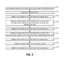
- FIG. 5is a flowchart of illustrative steps that may be used to operate a pixel with storage capacitors to obtain CDS and non-CDS samples in accordance with an embodiment of the present invention.
- FIG. 6is a flowchart of illustrative steps that may be used to operate a pixel with storage capacitors to obtain multiple CDS samples in accordance with an embodiment of the present invention.
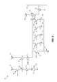
- FIG. 7is a diagram of an illustrative image pixel with multiple substrate layers that shows how an interconnect layer can be interposed between a source follower transistor and a sampling transistor in accordance with an embodiment of the present invention.
- FIG. 8is a diagram of an illustrative image pixel with multiple substrate layers that shows how an interconnect layer can be interposed between a source follower transistor and a floating diffusion region in accordance with an embodiment of the present invention.
- FIG. 9is a diagram of an illustrative image pixel with multiple substrate layers that shows how an interconnect layer can be interposed between a transfer transistor and a floating diffusion region in accordance with an embodiment of the present invention.
- Electronic devicessuch as digital cameras, computers, cellular telephones, and other electronic devices include image sensors that gather incoming image light to capture an image.
- the image sensorsmay include arrays of imaging pixels.
- the pixels in the image sensorsmay include photosensitive elements such as photodiodes that convert the incoming image light into image signals.
- Image sensorsmay have any number of pixels (e.g., hundreds or thousands or more).
- a typical image sensormay, for example, have hundreds of thousands or millions of pixels (e.g., megapixels).
- Image sensorsmay include control circuitry such as circuitry for operating the imaging pixels and readout circuitry for reading out image signals corresponding to the electric charge generated by the photosensitive elements.
- FIG. 1is a diagram of an illustrative imaging system that uses an image sensor with a global shutter.
- Imaging system 10 of FIG. 1may be a portable electronic device such as a camera, a cellular telephone, a video camera, or other imaging device that captures digital image data.
- Camera module 12may be used to convert incoming light into digital image data.
- Camera module 12may include one or more lenses 14 and one or more corresponding image sensors 16 .
- Image sensor 16may be an image sensor integrated circuit die with an array of image pixels 30 .
- Image pixels 30may each include a shutter element for controlling when charge is acquired on the image pixel.
- lens 14may focus light from a scene onto an image pixel array in image sensor 16 .
- Image sensor 16may provide corresponding digital image data to control circuitry such as storage and processing circuitry 18 .
- Circuitry 18may include one or more integrated circuits (e.g., image processing circuits, microprocessors, storage devices such as random-access memory and non-volatile memory, etc.) and may be implemented using components that are separate from camera module 12 and/or that form part of camera module 12 (e.g., circuits that form part of an integrated circuit that includes image sensors 16 or an integrated circuit within module 12 that is associated with image sensors 16 ). Image data that has been captured by camera module 12 may be further processed and/or stored using processing circuitry 18 . Processed image data may, if desired, be provided to external equipment (e.g., a computer or other device) using wired and/or wireless communications paths coupled to processing circuitry 18 . Processing circuitry 18 may be used in controlling the operation of image sensors 16 .
- integrated circuitse.g., image processing circuits, microprocessors, storage devices such as random-access memory and non-volatile memory, etc.
- FIG. 2is a circuit diagram of an illustrative image pixel 30 .
- pixel 30may include a photosensitive element such as photodiode 20 .
- a positive power supply voltage Vaamay be supplied at positive power supply terminals 22 and 23 .
- Incoming lightmay be collected by photodiode 20 after passing through a color filter structure.
- Photodiode 20generates charge (e.g., electrons) in response to receiving impinging photons. The amount of charge that is collected by photodiode 20 depends on the intensity of the impinging light and the exposure duration (or integration time).
- Pixel 30may include a floating diffusion region and a reset transistor for resetting the charge at the floating diffusion region.
- reset transistor 26Before an image is acquired, reset transistor 26 (RST 1 ) may be turned on to reset charge storage node 28 (sometimes referred to as floating diffusion region FD 1 ) to Vaa. Reset transistor 26 may be turned off after FD 1 has been reset to allow charge to be stored in FD 1 .
- Charge generated in photodiode 20may be stored in charge storage region 28 (FD 1 ).
- Pixel 30may include a transfer gate (transistor) 38 .
- Transfer transistor 38 ( 38 )may be turned on to transfer charge from photodiode 20 to floating diffusion region 28 .
- Floating diffusion region 28may be a doped semiconductor region (e.g., a region in a silicon substrate that is doped by ion implantation, impurity diffusion, or other doping process).
- Pixel 30may also include a source-follower transistor 40 (SF 1 ) that is coupled to power supply voltage Vaa at terminal 23 .
- SF 1may also be coupled to sampling transistor 42 (SAMP).
- Pixel 30may include a number of capacitors, such as capacitors 52 , 54 , 56 , and 58 (C 1 , C 2 , C 3 , and C 4 respectively).
- Capacitors 52 , 54 , 56 , and 58may be used to store charge from FD 1 .
- Each capacitormay be associated with a respective transistor.
- transistor 60 (S 1 )may be associated with storage capacitor 52
- transistor 62 (S 2 )may be associated with storage capacitor 54
- transistor 64 (S 3 )may be associated with storage capacitor 56
- transistor 66 (S 4 )may be associated with storage capacitor 58 .
- An additional floating diffusion region 68 (FD 2 ) and reset transistor 70 (RST 2 )may be provided in pixel 30 .
- Reset transistor 70may be asserted to couple floating diffusion region 68 to power supply terminal 74 , which may reset the charge at FD 2 .
- Floating diffusion region 68may be a doped semiconductor region (e.g., a region in a silicon substrate that is doped by ion implantation, impurity diffusion, or other doping process).
- Pixel 30may also include charge readout circuitry.
- the charge readout circuitrymay include row-select transistor 76 (RS) and source-follower transistor 78 (SF 2 ). SF 2 may be coupled to power supply terminal 79 .
- Transistor 76may have a gate that is controlled by a row select signal. When the row select signal is asserted, transistor 76 is turned on and a corresponding signal Vout (e.g., an output signal having a magnitude that is proportional to the amount of charge at floating diffusion node 68 ) is passed onto output path 80 .
- Voute.g., an output signal having a magnitude that is proportional to the amount of charge at floating diffusion node 68
- a column readout pathsuch as output line 80 may be associated with each column of pixels 30 (e.g., each image pixel 30 in a column may be coupled to output line 80 through an associated row-select transistor 76 ).
- the row select signalmay be asserted to read out signal Vout from a selected image pixel onto column readout path 80 .
- Image data Voutmay be fed to processing circuitry 18 for further processing.
- the circuitry of FIG. 2is merely illustrative. If desired, pixel 30 may include other pixel circuitry.
- pixel 30may include a pixel reset transistor that is coupled between photodiode 20 and a power supply terminal. This type of pixel reset transistor may reset photodiode 20 to the power supply voltage when turned on and allow the photodiode to accumulate photo-generated charge when turned off.
- pixel 30may also be provided with an additional transistor used to implement a dual conversion gain mode.
- pixel 30may be operable in a high conversion gain mode and in a low conversion gain mode. If the additional transistor is disabled, pixel 30 will be placed in a high conversion gain mode. If the additional transistor is enabled, pixel 30 will be placed in a low conversion gain mode.
- the additional transistormay be coupled to a capacitor. When the additional transistor is turned on, the capacitor may be switched into use to provide floating diffusion FD with additional capacitance. This results in lower conversion gain for pixel 30 . When the additional transistor is turned off, the additional loading of the capacitor is removed and the pixel reverts to a relatively higher pixel conversion gain configuration.
- positive power supply terminals 22 , 23 , 74 , and 79are depicted as all being separate entities. It should be noted that this example is merely illustrative. If desired, one, two, three, or four power supply terminals may be provided. More than one line may be coupled to any or all power supply terminals in the pixel. The power supply terminals may each provide the same power supply voltage or may provide different power supply voltages if desired.
- capacitors C 1 , C 2 , C 3 , and C 4may be used to store charge from floating diffusion 28 .
- charge from floating diffusion 28may be stored in a storage capacitor.
- a storage capacitormay be selected to store charge from floating diffusion 28 by asserting the transistor that is associated with the desired storage capacitor.
- S 1may be turned on while RST 2 , S 2 , S 3 , and S 4 are all turned off.
- charge from FD 1may be stored in C 1 when SAMP is turned on.
- S 2 and SAMPmay be turned on while RST 2 , S 1 , S 3 , and S 4 are all turned off to store charge in C 2 .
- S 3 and SAMPmay be turned on while RST 2 , S 1 , S 2 , and S 4 are all turned off to store charge in C 3 .
- S 4 and SAMPmay be turned on while RST 2 , S 1 , S 2 , and S 3 are all turned off to store charge in C 4 .
- various samples of charge from FD 1may be stored in pixel 30 at the same time. For example, samples may be stored in C 1 , C 2 , C 3 , and C 4 simultaneously.
- the respective transistore.g., S 1 , S 2 , S 3 , or S 4
- row select transistor 76may be asserted.
- RST 2may be briefly turned on to reset FD 2 .
- S 1 and RSmay be turned on.
- the charge from C 1may then be sampled from FD 2 and output via output line 80 .
- asserting S 2 , S 3 , or S 4individually will sample the charge at C 2 , C 3 , or C 4 .
- Sampling transistor 42may be turned off throughout the read out of the pixel.
- the pixel arrangement shown in FIG. 2offers many advantages. Charge from various samples may be stored in the storage capacitors. This may allow implementation of a global shutter. In a global shutter, every pixel in an image sensor accumulates charge simultaneously. For complementary metal-oxide semiconductor (CMOS) image sensors, the charge may then be stored in an intermediate charge storage region before being read out. In FIG. 2 , multiple intermediate charge storage regions are provided. This may allow high dynamic range images (which require at least two samples with different integration times) to be obtained with a global shutter.
- CMOScomplementary metal-oxide semiconductor
- the arrangement of pixel 30may also allow for correlated double sampling (CDS) to be implemented with a global shutter.
- CDScorrelated double sampling
- charge storage regionsare reset (e.g., when FD 1 and FD 2 are reset by reset transistors RST 1 and RST 2 )
- reset noisesometimes referred to as kTC noise
- the charge at a floating diffusion regionmay be sampled after reset and before charge transfer from the photodiode.
- the charge at the floating diffusion regionmay be sampled again after charge transfer from the photodiode.
- the first sample valuemay be subtracted from the second sample value to determine how much charge was generated by the photodiode (by eliminating charge at the floating diffusion region that is unassociated with incident light).
- correlated double samplingmay be used.
- the reset valuemay be stored on a first storage capacitor and the sample value may be stored on a second storage capacitor.
- FIG. 3An illustrative timing diagram for operation of pixel 30 in FIG. 2 is shown in FIG. 3 .
- the timing diagram of FIG. 3is merely an example, and it should be understood that a wide variety of other timing schemes may be used with pixel 30 .
- the timing diagram of FIG. 3begins with a first integration time (t int1 ).
- Photodiode 20may accumulate photo-generated charge during t int1 , as well as during a second integration time (t int2 ) and a third integration time (t int3 ).
- FD 1 and FD 2may be reset by turning on reset transistors RST 1 and RST 2 at assertions 82 and 84 . This may couple FD 1 and FD 2 to power supply voltage terminals 22 and 74 , respectively, and ensure that no excess charge is present in the floating diffusion regions.
- S 1may also be turned on at assertion 88 .
- the reset level at FD 1may be sampled.
- sampling transistor SAMPmay be asserted at assertion 86 . Because RST 2 , S 2 , S 3 , and S 4 are all turned off during assertions 86 and 88 , the charge from FD 1 will be stored in C 1 when SAMP and S 1 are asserted.
- reset transistor RST 2may be asserted at assertion 90 .
- S 2may be asserted at assertion 96 .
- the transfer transistor (TX)may be turned on at assertion 92 . This will transfer charge from photodiode 20 to FD 1 .
- the end of assertion 92coincides with the end of t int1 and the beginning of t int2 .
- the charge at FD 1corresponds to the amount of charge accumulated in photodiode 20 during t int1 .
- This valuemay be sampled by asserting sample transistor SAMP at assertion 94 . Because RST 2 , S 1 , S 3 , and S 4 are all turned off during assertions 94 and 96 , the charge from FD 1 will be stored in C 2 when SAMP and S 2 are asserted.
- reset transistor RST 2may be asserted at assertion 98 and S 3 may be asserted at assertion 104 .
- the transfer transistor (TX)may be turned on at assertion 100 . This will transfer charge from photodiode 20 to FD 1 .
- the end of assertion 100coincides with the end of t int2 and the beginning of t int3 .
- the charge at FD 1corresponds to the amount of charge accumulated in photodiode 20 during t int2 .
- This valuemay be sampled by asserting sample transistor SAMP at assertion 102 . Because RST 2 , S 1 , S 2 , and S 4 are all turned off during assertions 102 and 104 , the charge from FD 1 will be stored in C 3 when SAMP and S 3 are asserted.
- reset transistor RST 2may be asserted at assertion 106 and S 4 may be asserted at assertion 112 .
- the transfer transistor (TX)may be turned on at assertion 108 . This will transfer charge from photodiode 20 to FD 1 .
- the end of assertion 108coincides with the end of t int3 .
- the charge at FD 1corresponds to the amount of charge accumulated in photodiode 20 during t int3 .
- This valuemay be sampled by asserting sample transistor SAMP and transistor S 4 at assertion 110 . Because RST 2 , S 1 , S 2 , and S 3 are all turned off during assertions 110 and 112 , the charge from FD 1 will be stored in C 4 when SAMP and S 4 are asserted.
- each storage capacitormay have a corresponding sample.
- C 1may have the reset value stored
- C 2may have the t int1 sample stored
- C 3may have the t int2 sample stored
- C 4may have the t int3 stored.
- the sampling of pixel 30may be completed globally, meaning every pixel in image sensor 16 may simultaneously follow the timing diagram in FIG. 3 .
- t int1is shown as being longer than t int2 and t int3
- t int2is shown as being longer than t int3 .
- this exampleis merely illustrative.
- FIG. 4is a timing diagram of pixel 30 during sample read out. This portion of the pixel operation may not be completed globally. For example, the samples of each row of pixels may be read sequentially as opposed to simultaneously.
- reset transistor RST 2may be asserted at assertion 120 to reset FD 2 .
- S 1may also be asserted at assertion 122 to read out the charge stored in storage capacitor C 1 .
- FD 2may be reset again at assertion 124 .
- S 2may also be turned on at assertion 126 to read out the charge stored in storage capacitor C 2 .
- FD 2may be reset at assertion 128 .
- S 1may also be asserted at assertion 130 to read out the charge stored in storage capacitor C 1 .
- FD 2may be reset again at assertion 132 .
- S 3may also be turned on at assertion 134 to read out the charge stored in storage capacitor C 3 .
- FD 2may be reset at assertion 136 .
- S 1may also be asserted at assertion 138 to read out the charge stored in storage capacitor C 1 .
- FD 2may be reset again at assertion 140 .
- S 4may also be turned on at assertion 142 to read out the charge stored in storage capacitor C 4 .
- Sampling C 1 at assertions 130 and 138may help eliminate noise associated with the reset value of capacitors C 1 , C 2 , C 3 , and C 4 .
- C 1Before assertion 122 , C 1 may store charge associated with the reset level of FD 1 (as described in connection with FIG. 3 ).
- Sampling C 1 at assertion 122enables use of a correlated double sampling (CDS) technique to account for reset noise at FD 1 .
- CDScorrelated double sampling
- sampling C 1 at assertions 130 and 138will not account for FD 1 reset noise, the sampling may help account for the noise associated with RST 2 . However, these samplings may be omitted if desired (e.g., assertions 128 , 130 , 136 , and 138 may be omitted during read out).
- pixel 30may have one storage capacitor, two storage capacitors, three storage capacitors, four storage capacitors, five storage capacitors, six storage capacitors, seven storage capacitors, eight storage capacitors, or more than eight storage capacitors.
- only the first samplemay be corrected for reset noise of the first floating diffusion region.
- the longest integration timemay be completed first.
- the longest integration timemay be associated with low light levels and thus may be the most sensitive to reset noise.
- the most sensitive sampleis corrected.
- the subsequent samplesmay be less sensitive to reset noise, and not accounting for the reset noise may not substantially affect the image quality.
- the first integration timemay be the shortest integration time, the longest integration time, or an intermediate integration time.
- each integration timemay have any desired length, and the integration times may be arranged in any desired order.
- sampling the reset level for only the first integration periodis merely illustrative.
- a pixel with four capacitorsmay sample two reset values and two sample values (e.g., two different integration periods and their respective reset values may be sampled).
- one storage capacitoris required for sampling an integration time without accounting for FD 1 reset noise (non-CDS samples), while two storage capacitors are required for sampling an integration time and accounting for reset noise (CDS samples). Any combination of these samples may be used, limited only by how many capacitors are present in the pixel. For example, if pixel 30 includes four capacitors, the image sensor may be used to obtain four non-CDS samples, one CDS sample and two non-CDS samples (e.g., FIG. 3 ), or two CDS samples. Pixel 30 may include two capacitors. In these embodiments, pixel 30 may be used to obtain one CDS sample or two non-CDS samples. Pixel 30 may include three storage capacitors.
- pixel 30may be used to obtain three non-CDS samples or one CDS sample and one non-CDS sample. At least two samples are required for a high dynamic range (HDR) image. More samples may increase the dynamic range of the image. By requiring two storage capacitors, CDS samples may limit how many samples can be acquired by a given pixel (possibly reducing dynamic range), but will result in a less noisy image. The specific scene to be imaged or the preferences of the user of the imaging system may dictate what sampling scheme is used.
- HDRhigh dynamic range
- FIGS. 5 and 6Illustrative methods of operating an image pixel such as image pixel 30 from FIG. 2 are shown in FIGS. 5 and 6 .
- a flowchartshows steps for collecting one CDS sample and two non-CDS samples in storage capacitors.
- the photodiodemay begin accumulating charge for a first integration time (e.g., t int1 ).
- FD 1may be reset (e.g., using reset transistor 26 ). After resetting the charge at FD 1 , the charge at FD 1 may be sampled and the charge stored in storage capacitor C 1 at step 506 .
- chargemay be transferred from the photodiode to FD 1 .
- Chargemay also start accumulating for a second integration time (e.g., t int2 ).
- the charge at FD 1(which accumulated in the photodiode during t int1 ) may be sampled and the charge stored in capacitor C 2 .
- chargemay be transferred from the photodiode to FD 1 .
- Chargemay also start accumulating for a third integration time (e.g., t int3 ).
- the charge at FD 1(which accumulated in the photodiode during t int2 ) may be sampled and the charge stored in capacitor C 3 .
- chargemay be transferred from the photodiode to FD 1 .
- the charge at FD 1(which accumulated in the photodiode during t int3 ) may be sampled and the charge stored in capacitor C 4 .
- This methodenables the collection of one CDS sample (in capacitors C 1 and C 2 ) and two non-CDS samples (in capacitors C 3 and C 4 , respectively).
- a flowchartshows steps for collecting two CDS samples in storage capacitors.
- the photodiodemay begin accumulating charge for a first integration time (e.g., t int1 ).
- FD 1may be reset (e.g., using reset transistor 26 ).
- the charge at FD 1may be sampled and the charge stored in storage capacitor C 1 at step 606 .
- chargemay be transferred from the photodiode to FD 1 .
- the charge at FD 1may be sampled and the charge stored in storage capacitor C 2 .
- chargemay start accumulating for a second integration time (e.g., t int2 ).
- FD 1may be reset (e.g., using reset transistor 26 ).
- the charge at FD 1may be sampled and the charge stored in storage capacitor C 3 at step 616 .
- chargemay be transferred from the photodiode to FD 1 .
- the charge at FD 1may be sampled and the charge stored in storage capacitor C 4 . This method enables the collection of two CDS samples, one that is stored in C 1 and C 2 , and another that is stored in C 3 and C 4 .
- Photodiode 20may be formed in a substrate.
- the substratemay be a wafer, which is a layer of semiconductor material such as silicon.
- the substratemay be crystalline silicon or another desired material.
- Photodiode 20may be formed from n-type doped silicon.
- the substrate surrounding photodiode 20may be p-type doped silicon.
- the photodiodemay be formed from p-type doped silicon and be surrounded by n-type doped silicon.
- Photodiode 20may be covered by a passivation layer, a color filter layer, a planarization layer, and a microlens.
- the passivation layer and planarization layermay be formed from dielectric materials.
- the color filter layermay be a part of a larger color filter array.
- each pixel in image sensor 14may have an individual color filter layer that is part of the color filter array.
- Image sensor 14may include a Bayer color filter array in which vertically and horizontally adjacent color filters in the array are of different colors.
- the Bayer color filter arrayincludes red, green, and blue color filters. A single red, green, blue, cyan, magenta, yellow, near-infrared, infrared, or clear color filter may be formed over photodiode 20 .
- the color filter formed over photodiode 20may have areas that pass colored light and areas that are clear (i.e., that pass visible spectrum light).
- a microlensmay be formed over each pixel in image sensor 14 . Each microlens may direct light towards a respective photodiode.
- the pixel circuitry in the pixel of FIG. 2may all be formed in a single substrate (e.g., a single wafer). However, the storage capacitors C 1 , C 2 , C 3 , and C 4 may take up space in the substrate and limit the amount of space available for photodiode 20 . Therefore, in certain embodiments, two substrates may be used to form the pixel circuitry of pixels such as pixel 30 .
- the substrate layersmay be silicon wafers or another desired semiconductor material.
- an upper substrate layer 150 in pixel 30may be connected to a lower substrate layer 152 .
- Upper and lower substrate layers 150 and 152may be crystalline silicon or any other desired material.
- An interconnect layermay be used to connect upper substrate layer 150 to lower substrate layer 152 .
- Interconnect layer 154may be formed from a conductive material such as metal (e.g., copper). In certain embodiments, the interconnect layer may include solder.
- the interconnect layermay also be a through silicon via (TSV).
- interconnect layer 154may couple source follower transistor 40 (SF 1 ) to sampling transistor 42 (SAMP). Interconnect layer 154 may be coupled directly to SF 1 and SAMP without any intervening transistors.
- the interconnect layermay enable photodiode 20 to have a larger size than if all of the pixel circuitry was in a single wafer.
- Another advantage of interconnect layer 154is that it may act as a reflector for photodiode 20 . As photons pass through photodiode 36 , some of the photons may be absorbed by the photodiode and converted to charge. However, some photons may pass through the photodiode without being converted to charge. These photons may reflect off of interconnect layer 154 and travel upwards towards the photodiode. This increases the probability that the photon will be converted to charge by the photodiode.
- Interconnect layer 154does not necessarily have to be positioned between transistors 40 and 42 .
- the interconnect layermay be positioned between FD 1 and SF 1 .
- Interconnect layer 154may be coupled directly to SF 1 and FD 1 without any intervening transistors.
- interconnect layer 154may be positioned between FD 1 and transfer transistor 38 (TX), as shown in FIG. 9 .
- TXtransfer transistor 38
- an imaging pixelmay include an upper substrate layer, a lower substrate layer, a floating diffusion region, a photodiode in the upper substrate layer that is coupled to the floating diffusion region, an interconnect layer interposed between the upper substrate layer and the lower substrate layer that couples the upper substrate layer to the lower substrate layer, and a first storage capacitor in the lower substrate layer.
- the imaging pixelmay also include a source follower transistor coupled to the floating diffusion region, an additional floating diffusion region, an additional source follower transistor coupled to the additional floating diffusion region, and a sampling transistor coupled between the source follower transistor and the additional floating diffusion region.
- the interconnect layermay be interposed between the source follower transistor and the sampling transistor.
- the floating diffusion region and the source follower transistormay be formed in the upper substrate layer, and the sampling transistor, the additional floating diffusion region, and the additional source follower transistor may be formed in the lower substrate layer.
- the imaging pixelmay also include second and third storage capacitors formed in the lower substrate layer.
- the imaging pixelmay include a source follower transistor formed in the lower substrate layer that is coupled to the floating diffusion region.
- the floating diffusion regionmay be formed in the upper substrate layer, and the interconnect layer may be interposed between the floating diffusion region and the source follower transistor.
- the imaging pixelmay also include second and third storage capacitors formed in the lower substrate layer.
- the imaging pixelmay include a transfer transistor formed in the upper substrate layer that is coupled to the floating diffusion region.
- the floating diffusion regionmay be formed in the lower substrate layer and the interconnect layer may be interposed between the transfer transistor and the floating diffusion region.
- the imaging pixelmay also include second and third storage capacitors formed in the lower substrate layer.
- an imaging pixelmay include a first floating diffusion region, a photodiode coupled to the first floating diffusion region, a first source follower transistor coupled to the first floating diffusion region, a second floating diffusion region, a second source follower transistor coupled to the second floating diffusion region, a first storage capacitor, a second storage capacitor, and a third storage capacitor.
- the imaging pixelmay also include a sampling transistor interposed between the second floating diffusion region and the first source follower transistor.
- the imaging pixelmay also include a first reset transistor interposed between the first floating diffusion region and a first positive power supply terminal and a second reset transistor interposed between the second floating diffusion region and a second positive power supply terminal.
- the imaging pixelmay also include a transistor interposed between the sampling transistor and the first storage capacitor, a transistor interposed between the sampling transistor and the second storage capacitor, and a transistor interposed between the sampling transistor and the third storage capacitor.
- the imaging pixelmay also include a row select transistor interposed between an output line and the second source follower transistor.
- a method of operating an imaging pixelmay be provided.
- the imaging pixelmay include a photodiode, a floating diffusion region, a first storage capacitor, a second storage capacitor, and a third storage capacitor.
- the methodmay include accumulating a first amount of charge for a first time period with the photodiode, resetting the floating diffusion region to a power supply voltage, sampling a second amount of charge at the floating diffusion region and storing the second amount of charge in the first storage capacitor after resetting the floating diffusion region to the power supply voltage, transferring the first amount of charge to the floating diffusion region, sampling the first amount of charge at the floating diffusion region and storing the first amount of charge in the second storage capacitor after transferring the first amount of charge to the floating diffusion region, accumulating a third amount of charge for a second time period with the photodiode, transferring the third amount of charge to the floating diffusion region, and sampling the third amount of charge at the floating diffusion region and storing the third amount of charge in the third storage capacitor after transferring
- the imaging pixelmay also include a fourth storage capacitor.
- the methodmay also include accumulating a fourth amount of charge for a third time period with the photodiode, transferring the fourth amount of charge to the floating diffusion region, and sampling the fourth amount of charge at the floating diffusion region and storing the fourth amount of charge in the fourth storage capacitor after transferring the fourth amount of charge to the floating diffusion region.
- the methodmay also include resetting the floating diffusion region to the power supply voltage before transferring the third amount of charge to the floating diffusion region and after sampling the second amount of charge at the floating diffusion region, and sampling a fourth amount of charge at the floating diffusion region and storing the fourth amount of charge in the fourth storage capacitor after resetting the floating diffusion region to the power supply voltage and before transferring the third amount of charge to the floating diffusion region.
- the first time periodmay be longer than the second time period.
- the imaging pixelmay also include a first source follower transistor coupled to the floating diffusion region, an additional floating diffusion region, and a second source follower transistor coupled to the additional floating diffusion region.
- the imaging pixelmay also include a transistor interposed between the first source follower transistor and the additional floating diffusion region, and sampling the first amount of charge at the floating diffusion region and storing the first amount of charge in the second storage capacitor may include turning on the transistor.
Landscapes
- Engineering & Computer Science (AREA)
- Multimedia (AREA)
- Signal Processing (AREA)
- Solid State Image Pick-Up Elements (AREA)
- Transforming Light Signals Into Electric Signals (AREA)
Abstract
Description
- This relates generally to imaging systems, and more particularly, to imaging systems with global shutter functionality.
- Modern electronic devices such a cellular telephones, cameras, and computers often use digital image sensors. Imagers (i.e., image sensors) often include a two-dimensional array of image sensing pixels. Each pixel typically includes a photosensor such as a photodiode that receives incident photons (light) and converts the photons into electrical signals.
- Conventional image sensors are fabricated on a semiconductor substrate using complementary metal-oxide-semiconductor (CMOS) technology or charge-coupled device (CCD) technology. In CMOS image sensors, a rolling shutter or a global shutter may be used. In a global shutter, every pixel in the image sensor may simultaneously capture an image, whereas in a rolling shutter each row of pixels may sequentially capture an image. In CMOS image sensors with a global shutter, a charge storage region is typically incorporated into each pixel to store charge from the photodiode until read out. However, these pixels may not be able to acquire high dynamic range (HDR) images, which limits the functionality of the image sensor. Additionally, these pixels may not be able to acquire images using correlated double sampling (CDS) techniques. This may increase noise in the pixels and decrease the image quality of the image sensor.
- It would therefore be desirable to be able to provide improved CMOS image sensors with global shutter functionality.
FIG. 1 is a diagram of an illustrative imaging system that may include an image sensor having image pixels with a global shutter in accordance with an embodiment of the present invention.FIG. 2 is a diagram of an illustrative image pixel that uses at least one storage capacitor for a global shutter in accordance with an embodiment of the present invention.FIG. 3 is an illustrative timing diagram for collecting image samples with a pixel such as the pixel inFIG. 2 in accordance with an embodiment of the present invention.FIG. 4 is an illustrative timing diagram for reading out image samples with a pixel such as the pixel inFIG. 2 in accordance with an embodiment of the present invention.FIG. 5 is a flowchart of illustrative steps that may be used to operate a pixel with storage capacitors to obtain CDS and non-CDS samples in accordance with an embodiment of the present invention.FIG. 6 is a flowchart of illustrative steps that may be used to operate a pixel with storage capacitors to obtain multiple CDS samples in accordance with an embodiment of the present invention.FIG. 7 is a diagram of an illustrative image pixel with multiple substrate layers that shows how an interconnect layer can be interposed between a source follower transistor and a sampling transistor in accordance with an embodiment of the present invention.FIG. 8 is a diagram of an illustrative image pixel with multiple substrate layers that shows how an interconnect layer can be interposed between a source follower transistor and a floating diffusion region in accordance with an embodiment of the present invention.FIG. 9 is a diagram of an illustrative image pixel with multiple substrate layers that shows how an interconnect layer can be interposed between a transfer transistor and a floating diffusion region in accordance with an embodiment of the present invention.- Electronic devices such as digital cameras, computers, cellular telephones, and other electronic devices include image sensors that gather incoming image light to capture an image. The image sensors may include arrays of imaging pixels. The pixels in the image sensors may include photosensitive elements such as photodiodes that convert the incoming image light into image signals. Image sensors may have any number of pixels (e.g., hundreds or thousands or more). A typical image sensor may, for example, have hundreds of thousands or millions of pixels (e.g., megapixels). Image sensors may include control circuitry such as circuitry for operating the imaging pixels and readout circuitry for reading out image signals corresponding to the electric charge generated by the photosensitive elements.
FIG. 1 is a diagram of an illustrative imaging system that uses an image sensor with a global shutter.Imaging system 10 ofFIG. 1 may be a portable electronic device such as a camera, a cellular telephone, a video camera, or other imaging device that captures digital image data.Camera module 12 may be used to convert incoming light into digital image data.Camera module 12 may include one ormore lenses 14 and one or morecorresponding image sensors 16.Image sensor 16 may be an image sensor integrated circuit die with an array ofimage pixels 30.Image pixels 30 may each include a shutter element for controlling when charge is acquired on the image pixel.- During image capture operations,
lens 14 may focus light from a scene onto an image pixel array inimage sensor 16.Image sensor 16 may provide corresponding digital image data to control circuitry such as storage andprocessing circuitry 18. Circuitry 18 may include one or more integrated circuits (e.g., image processing circuits, microprocessors, storage devices such as random-access memory and non-volatile memory, etc.) and may be implemented using components that are separate fromcamera module 12 and/or that form part of camera module12 (e.g., circuits that form part of an integrated circuit that includesimage sensors 16 or an integrated circuit withinmodule 12 that is associated with image sensors16). Image data that has been captured bycamera module 12 may be further processed and/or stored usingprocessing circuitry 18. Processed image data may, if desired, be provided to external equipment (e.g., a computer or other device) using wired and/or wireless communications paths coupled toprocessing circuitry 18.Processing circuitry 18 may be used in controlling the operation ofimage sensors 16.FIG. 2 is a circuit diagram of anillustrative image pixel 30. As shown inFIG. 2 ,pixel 30 may include a photosensitive element such asphotodiode 20. A positive power supply voltage Vaa may be supplied at positivepower supply terminals photodiode 20 after passing through a color filter structure. Photodiode20 generates charge (e.g., electrons) in response to receiving impinging photons. The amount of charge that is collected byphotodiode 20 depends on the intensity of the impinging light and the exposure duration (or integration time).Pixel 30 may include a floating diffusion region and a reset transistor for resetting the charge at the floating diffusion region. Before an image is acquired, reset transistor26 (RST1) may be turned on to reset charge storage node28 (sometimes referred to as floating diffusion region FD1) to Vaa.Reset transistor 26 may be turned off after FD1 has been reset to allow charge to be stored in FD1.- Charge generated in
photodiode 20 may be stored in charge storage region28 (FD1).Pixel 30 may include a transfer gate (transistor)38. Transfer transistor38 (38) may be turned on to transfer charge fromphotodiode 20 to floatingdiffusion region 28.Floating diffusion region 28 may be a doped semiconductor region (e.g., a region in a silicon substrate that is doped by ion implantation, impurity diffusion, or other doping process). Pixel 30 may also include a source-follower transistor40 (SF1) that is coupled to power supply voltage Vaa atterminal 23. SF1 may also be coupled to sampling transistor42 (SAMP).Pixel 30 may include a number of capacitors, such ascapacitors Capacitors storage capacitor 52, transistor62 (S2) may be associated withstorage capacitor 54, transistor64 (S3) may be associated withstorage capacitor 56, and transistor66 (S4) may be associated withstorage capacitor 58.- An additional floating diffusion region68 (FD2) and reset transistor70 (RST2) may be provided in
pixel 30.Reset transistor 70 may be asserted to couple floatingdiffusion region 68 topower supply terminal 74, which may reset the charge at FD2.Floating diffusion region 68 may be a doped semiconductor region (e.g., a region in a silicon substrate that is doped by ion implantation, impurity diffusion, or other doping process). Pixel 30 may also include charge readout circuitry. The charge readout circuitry may include row-select transistor76 (RS) and source-follower transistor78 (SF2). SF2 may be coupled topower supply terminal 79.Transistor 76 may have a gate that is controlled by a row select signal. When the row select signal is asserted,transistor 76 is turned on and a corresponding signal Vout (e.g., an output signal having a magnitude that is proportional to the amount of charge at floating diffusion node68) is passed ontooutput path 80.- In a typical image pixel array configuration, there are numerous rows and columns of
pixels 30. A column readout path such asoutput line 80 may be associated with each column of pixels30 (e.g., eachimage pixel 30 in a column may be coupled tooutput line 80 through an associated row-select transistor76). The row select signal may be asserted to read out signal Vout from a selected image pixel ontocolumn readout path 80. Image data Vout may be fed to processingcircuitry 18 for further processing. The circuitry ofFIG. 2 is merely illustrative. If desired,pixel 30 may include other pixel circuitry. - For example, although not shown in
FIG. 2 ,pixel 30 may include a pixel reset transistor that is coupled betweenphotodiode 20 and a power supply terminal. This type of pixel reset transistor may resetphotodiode 20 to the power supply voltage when turned on and allow the photodiode to accumulate photo-generated charge when turned off. - If desired,
pixel 30 may also be provided with an additional transistor used to implement a dual conversion gain mode. In particular,pixel 30 may be operable in a high conversion gain mode and in a low conversion gain mode. If the additional transistor is disabled,pixel 30 will be placed in a high conversion gain mode. If the additional transistor is enabled,pixel 30 will be placed in a low conversion gain mode. The additional transistor may be coupled to a capacitor. When the additional transistor is turned on, the capacitor may be switched into use to provide floating diffusion FD with additional capacitance. This results in lower conversion gain forpixel 30. When the additional transistor is turned off, the additional loading of the capacitor is removed and the pixel reverts to a relatively higher pixel conversion gain configuration. - In
FIG. 2 , positivepower supply terminals - During operation of
pixel 30, capacitors C1, C2, C3, and C4 may be used to store charge from floatingdiffusion 28. When samplingtransistor 42 is asserted, charge from floatingdiffusion 28 may be stored in a storage capacitor. A storage capacitor may be selected to store charge from floatingdiffusion 28 by asserting the transistor that is associated with the desired storage capacitor. For example, S1 may be turned on while RST2, S2, S3, and S4 are all turned off. In this example, charge from FD1 may be stored in C1 when SAMP is turned on. In another example, S2 and SAMP may be turned on while RST2, S1, S3, and S4 are all turned off to store charge in C2. In yet another example, S3 and SAMP may be turned on while RST2, S1, S2, and S4 are all turned off to store charge in C3. Finally, S4 and SAMP may be turned on while RST2, S1, S2, and S3 are all turned off to store charge in C4. Using this scheme, various samples of charge from FD1 may be stored inpixel 30 at the same time. For example, samples may be stored in C1, C2, C3, and C4 simultaneously. - When read out of the charges stored in the storage capacitors is desired, the respective transistor (e.g., S1, S2, S3, or S4) and row
select transistor 76 may be asserted. For example, RST2 may be briefly turned on to reset FD2. Subsequently, S1 and RS may be turned on. The charge from C1 may then be sampled from FD2 and output viaoutput line 80. Similarly, asserting S2, S3, or S4 individually will sample the charge at C2, C3, or C4. Samplingtransistor 42 may be turned off throughout the read out of the pixel. - The pixel arrangement shown in
FIG. 2 offers many advantages. Charge from various samples may be stored in the storage capacitors. This may allow implementation of a global shutter. In a global shutter, every pixel in an image sensor accumulates charge simultaneously. For complementary metal-oxide semiconductor (CMOS) image sensors, the charge may then be stored in an intermediate charge storage region before being read out. InFIG. 2 , multiple intermediate charge storage regions are provided. This may allow high dynamic range images (which require at least two samples with different integration times) to be obtained with a global shutter. - The arrangement of
pixel 30 may also allow for correlated double sampling (CDS) to be implemented with a global shutter. When charge storage regions are reset (e.g., when FD1 and FD2 are reset by reset transistors RST1 and RST2), reset noise (sometimes referred to as kTC noise) may be present. To account for this noise, the charge at a floating diffusion region may be sampled after reset and before charge transfer from the photodiode. The charge at the floating diffusion region may be sampled again after charge transfer from the photodiode. The first sample value may be subtracted from the second sample value to determine how much charge was generated by the photodiode (by eliminating charge at the floating diffusion region that is unassociated with incident light). Becausepixel 30 has multiple storage capacitors, correlated double sampling may be used. For example, the reset value may be stored on a first storage capacitor and the sample value may be stored on a second storage capacitor. - An illustrative timing diagram for operation of
pixel 30 inFIG. 2 is shown inFIG. 3 . The timing diagram ofFIG. 3 is merely an example, and it should be understood that a wide variety of other timing schemes may be used withpixel 30. - The timing diagram of
FIG. 3 begins with a first integration time (tint1).Photodiode 20 may accumulate photo-generated charge during tint1, as well as during a second integration time (tint2) and a third integration time (tint3). Before sampling the charge fromphotodiode 20, FD1 and FD2 may be reset by turning on reset transistors RST1 and RST2 atassertions supply voltage terminals assertion 88. - After resetting FD1 and FD2, the reset level at FD1 may be sampled. To sample the reset level at FD1, sampling transistor SAMP may be asserted at
assertion 86. Because RST2, S2, S3, and S4 are all turned off duringassertions - After storing the reset level in storage capacitor C1, reset transistor RST2 may be asserted at
assertion 90. At the same time, S2 may be asserted atassertion 96. Next, the transfer transistor (TX) may be turned on atassertion 92. This will transfer charge fromphotodiode 20 to FD1. The end ofassertion 92 coincides with the end of tint1and the beginning of tint2. Immediately afterassertion 92, the charge at FD1 corresponds to the amount of charge accumulated inphotodiode 20 during tint1. This value may be sampled by asserting sample transistor SAMP atassertion 94. Because RST2, S1, S3, and S4 are all turned off duringassertions - After storing the tint1sample in storage capacitor C2, reset transistor RST2 may be asserted at
assertion 98 and S3 may be asserted atassertion 104. Next, the transfer transistor (TX) may be turned on atassertion 100. This will transfer charge fromphotodiode 20 to FD1. The end ofassertion 100 coincides with the end of tint2and the beginning of tint3. Immediately afterassertion 100, the charge at FD1 corresponds to the amount of charge accumulated inphotodiode 20 during tint2. This value may be sampled by asserting sample transistor SAMP atassertion 102. Because RST2, S1, S2, and S4 are all turned off duringassertions - After storing the tint2sample in storage capacitor C3, reset transistor RST2 may be asserted at
assertion 106 and S4 may be asserted atassertion 112. Next, the transfer transistor (TX) may be turned on at assertion108. This will transfer charge fromphotodiode 20 to FD1. The end of assertion108 coincides with the end of tint3. Immediately after assertion108, the charge at FD1 corresponds to the amount of charge accumulated inphotodiode 20 during tint3. This value may be sampled by asserting sample transistor SAMP and transistor S4 atassertion 110. Because RST2, S1, S2, and S3 are all turned off duringassertions - After storing the tint3sample in storage capacitor C4, each storage capacitor may have a corresponding sample. C1 may have the reset value stored, C2 may have the tint1sample stored, C3 may have the tint2sample stored, and C4 may have the tint3stored. The sampling of
pixel 30 may be completed globally, meaning every pixel inimage sensor 16 may simultaneously follow the timing diagram inFIG. 3 . In the example ofFIG. 3 , tint1is shown as being longer than tint2and tint3, while tint2is shown as being longer than tint3. However, this example is merely illustrative. FIG. 4 is a timing diagram ofpixel 30 during sample read out. This portion of the pixel operation may not be completed globally. For example, the samples of each row of pixels may be read sequentially as opposed to simultaneously. As shown inFIG. 4 , reset transistor RST2 may be asserted atassertion 120 to reset FD2. S1 may also be asserted atassertion 122 to read out the charge stored in storage capacitor C1. FD2 may be reset again atassertion 124. S2 may also be turned on atassertion 126 to read out the charge stored in storage capacitor C2.- After reading out the charges stored in storage capacitor C1 and C2, FD2 may be reset at
assertion 128. S1 may also be asserted atassertion 130 to read out the charge stored in storage capacitor C1. FD2 may be reset again atassertion 132. S3 may also be turned on atassertion 134 to read out the charge stored in storage capacitor C3. After reading out the charges stored in storage capacitor C1 and C3, FD2 may be reset atassertion 136. S1 may also be asserted atassertion 138 to read out the charge stored in storage capacitor C1. FD2 may be reset again atassertion 140. S4 may also be turned on atassertion 142 to read out the charge stored in storage capacitor C4. - Sampling C1 at
assertions assertion 122, C1 may store charge associated with the reset level of FD1 (as described in connection withFIG. 3 ). Sampling C1 atassertion 122 enables use of a correlated double sampling (CDS) technique to account for reset noise at FD1. After C1 is sampled atassertion 122, the reset level of FD1 is no longer available for sampling. However, there may also be noise associated with the reset of capacitors C1, C2, C3, and C4 and FD2. Although sampling C1 atassertions assertions - In the example of
FIG. 2 , four storage capacitors are depicted. However, this example is merely illustrative. If desired,pixel 30 may have one storage capacitor, two storage capacitors, three storage capacitors, four storage capacitors, five storage capacitors, six storage capacitors, seven storage capacitors, eight storage capacitors, or more than eight storage capacitors. - In certain embodiments, only the first sample (from the first integration time) may be corrected for reset noise of the first floating diffusion region. In these embodiments, the longest integration time may be completed first. The longest integration time may be associated with low light levels and thus may be the most sensitive to reset noise. By making the longest integration time the first integration time, the most sensitive sample is corrected. The subsequent samples may be less sensitive to reset noise, and not accounting for the reset noise may not substantially affect the image quality.
- The relative lengths of the integration times of
FIG. 3 are purely illustrative. If desired, the first integration time may be the shortest integration time, the longest integration time, or an intermediate integration time. In general, each integration time may have any desired length, and the integration times may be arranged in any desired order. Additionally, sampling the reset level for only the first integration period is merely illustrative. If desired, a pixel with four capacitors may sample two reset values and two sample values (e.g., two different integration periods and their respective reset values may be sampled). - In general, one storage capacitor is required for sampling an integration time without accounting for FD1 reset noise (non-CDS samples), while two storage capacitors are required for sampling an integration time and accounting for reset noise (CDS samples). Any combination of these samples may be used, limited only by how many capacitors are present in the pixel. For example, if
pixel 30 includes four capacitors, the image sensor may be used to obtain four non-CDS samples, one CDS sample and two non-CDS samples (e.g.,FIG. 3 ), or two CDS samples.Pixel 30 may include two capacitors. In these embodiments,pixel 30 may be used to obtain one CDS sample or two non-CDS samples.Pixel 30 may include three storage capacitors. In these embodiments,pixel 30 may be used to obtain three non-CDS samples or one CDS sample and one non-CDS sample. At least two samples are required for a high dynamic range (HDR) image. More samples may increase the dynamic range of the image. By requiring two storage capacitors, CDS samples may limit how many samples can be acquired by a given pixel (possibly reducing dynamic range), but will result in a less noisy image. The specific scene to be imaged or the preferences of the user of the imaging system may dictate what sampling scheme is used. - Illustrative methods of operating an image pixel such as
image pixel 30 fromFIG. 2 are shown inFIGS. 5 and 6 . InFIG. 5 , a flowchart shows steps for collecting one CDS sample and two non-CDS samples in storage capacitors. Atstep 502 inFIG. 5 , the photodiode may begin accumulating charge for a first integration time (e.g., tint1). Atstep 504, FD1 may be reset (e.g., using reset transistor26). After resetting the charge at FD1, the charge at FD1 may be sampled and the charge stored in storage capacitor C1 atstep 506. Atstep 508, charge may be transferred from the photodiode to FD1. Charge may also start accumulating for a second integration time (e.g., tint2). Atstep 510, the charge at FD1 (which accumulated in the photodiode during tint1) may be sampled and the charge stored in capacitor C2. Atstep 512, charge may be transferred from the photodiode to FD1. Charge may also start accumulating for a third integration time (e.g., tint3). Atstep 514, the charge at FD1 (which accumulated in the photodiode during tint2) may be sampled and the charge stored in capacitor C3. Atstep 516, charge may be transferred from the photodiode to FD1. Atstep 518, the charge at FD1 (which accumulated in the photodiode during tint3) may be sampled and the charge stored in capacitor C4. This method enables the collection of one CDS sample (in capacitors C1 and C2) and two non-CDS samples (in capacitors C3 and C4, respectively). - In
FIG. 6 , a flowchart shows steps for collecting two CDS samples in storage capacitors. Atstep 602 inFIG. 6 , the photodiode may begin accumulating charge for a first integration time (e.g., tint1). Atstep 604, FD1 may be reset (e.g., using reset transistor26). After resetting the charge at FD1, the charge at FD1 may be sampled and the charge stored in storage capacitor C1 atstep 606. Atstep 608, charge may be transferred from the photodiode to FD1. Atstep 610, the charge at FD1 may be sampled and the charge stored in storage capacitor C2. Atstep 612, charge may start accumulating for a second integration time (e.g., tint2). Atstep 614, FD1 may be reset (e.g., using reset transistor26). After resetting the charge at FD1, the charge at FD1 may be sampled and the charge stored in storage capacitor C3 atstep 616. Atstep 618, charge may be transferred from the photodiode to FD1. Atstep 620, the charge at FD1 may be sampled and the charge stored in storage capacitor C4. This method enables the collection of two CDS samples, one that is stored in C1 and C2, and another that is stored in C3 and C4. Photodiode 20 may be formed in a substrate. The substrate may be a wafer, which is a layer of semiconductor material such as silicon. The substrate may be crystalline silicon or another desired material.Photodiode 20 may be formed from n-type doped silicon. Thesubstrate surrounding photodiode 20 may be p-type doped silicon. In certain embodiments, the photodiode may be formed from p-type doped silicon and be surrounded by n-type doped silicon.Photodiode 20 may be covered by a passivation layer, a color filter layer, a planarization layer, and a microlens. The passivation layer and planarization layer may be formed from dielectric materials. The color filter layer may be a part of a larger color filter array. For example, each pixel inimage sensor 14 may have an individual color filter layer that is part of the color filter array.Image sensor 14 may include a Bayer color filter array in which vertically and horizontally adjacent color filters in the array are of different colors. The Bayer color filter array includes red, green, and blue color filters. A single red, green, blue, cyan, magenta, yellow, near-infrared, infrared, or clear color filter may be formed overphotodiode 20. In certain embodiments, the color filter formed overphotodiode 20 may have areas that pass colored light and areas that are clear (i.e., that pass visible spectrum light). A microlens may be formed over each pixel inimage sensor 14. Each microlens may direct light towards a respective photodiode.- The pixel circuitry in the pixel of
FIG. 2 may all be formed in a single substrate (e.g., a single wafer). However, the storage capacitors C1, C2, C3, and C4 may take up space in the substrate and limit the amount of space available forphotodiode 20. Therefore, in certain embodiments, two substrates may be used to form the pixel circuitry of pixels such aspixel 30. The substrate layers may be silicon wafers or another desired semiconductor material. - As shown in
FIG. 7 , anupper substrate layer 150 inpixel 30 may be connected to alower substrate layer 152. Upper andlower substrate layers upper substrate layer 150 tolower substrate layer 152.Interconnect layer 154 may be formed from a conductive material such as metal (e.g., copper). In certain embodiments, the interconnect layer may include solder. The interconnect layer may also be a through silicon via (TSV). - As shown in
FIG. 7 ,interconnect layer 154 may couple source follower transistor40 (SF1) to sampling transistor42 (SAMP).Interconnect layer 154 may be coupled directly to SF1 and SAMP without any intervening transistors. The interconnect layer may enablephotodiode 20 to have a larger size than if all of the pixel circuitry was in a single wafer. Another advantage ofinterconnect layer 154 is that it may act as a reflector forphotodiode 20. As photons pass through photodiode36, some of the photons may be absorbed by the photodiode and converted to charge. However, some photons may pass through the photodiode without being converted to charge. These photons may reflect off ofinterconnect layer 154 and travel upwards towards the photodiode. This increases the probability that the photon will be converted to charge by the photodiode. Interconnect layer 154 does not necessarily have to be positioned betweentransistors FIG. 8 the interconnect layer may be positioned between FD1 and SF1.Interconnect layer 154 may be coupled directly to SF1 and FD1 without any intervening transistors. In yet another embodiment,interconnect layer 154 may be positioned between FD1 and transfer transistor38 (TX), as shown inFIG. 9 .Interconnect layer 154 may be coupled directly to TX and FD1 without any intervening transistors.- In various embodiments of the invention, an imaging pixel may include an upper substrate layer, a lower substrate layer, a floating diffusion region, a photodiode in the upper substrate layer that is coupled to the floating diffusion region, an interconnect layer interposed between the upper substrate layer and the lower substrate layer that couples the upper substrate layer to the lower substrate layer, and a first storage capacitor in the lower substrate layer.
- The imaging pixel may also include a source follower transistor coupled to the floating diffusion region, an additional floating diffusion region, an additional source follower transistor coupled to the additional floating diffusion region, and a sampling transistor coupled between the source follower transistor and the additional floating diffusion region. The interconnect layer may be interposed between the source follower transistor and the sampling transistor. The floating diffusion region and the source follower transistor may be formed in the upper substrate layer, and the sampling transistor, the additional floating diffusion region, and the additional source follower transistor may be formed in the lower substrate layer. The imaging pixel may also include second and third storage capacitors formed in the lower substrate layer.
- In other embodiments, the imaging pixel may include a source follower transistor formed in the lower substrate layer that is coupled to the floating diffusion region. The floating diffusion region may be formed in the upper substrate layer, and the interconnect layer may be interposed between the floating diffusion region and the source follower transistor. The imaging pixel may also include second and third storage capacitors formed in the lower substrate layer.
- In yet another embodiment, the imaging pixel may include a transfer transistor formed in the upper substrate layer that is coupled to the floating diffusion region. The floating diffusion region may be formed in the lower substrate layer and the interconnect layer may be interposed between the transfer transistor and the floating diffusion region. The imaging pixel may also include second and third storage capacitors formed in the lower substrate layer.
- In various embodiments of the invention, an imaging pixel may include a first floating diffusion region, a photodiode coupled to the first floating diffusion region, a first source follower transistor coupled to the first floating diffusion region, a second floating diffusion region, a second source follower transistor coupled to the second floating diffusion region, a first storage capacitor, a second storage capacitor, and a third storage capacitor.
- The imaging pixel may also include a sampling transistor interposed between the second floating diffusion region and the first source follower transistor. The imaging pixel may also include a first reset transistor interposed between the first floating diffusion region and a first positive power supply terminal and a second reset transistor interposed between the second floating diffusion region and a second positive power supply terminal. The imaging pixel may also include a transistor interposed between the sampling transistor and the first storage capacitor, a transistor interposed between the sampling transistor and the second storage capacitor, and a transistor interposed between the sampling transistor and the third storage capacitor. The imaging pixel may also include a row select transistor interposed between an output line and the second source follower transistor.
- In various embodiments of the invention, a method of operating an imaging pixel may be provided. The imaging pixel may include a photodiode, a floating diffusion region, a first storage capacitor, a second storage capacitor, and a third storage capacitor. The method may include accumulating a first amount of charge for a first time period with the photodiode, resetting the floating diffusion region to a power supply voltage, sampling a second amount of charge at the floating diffusion region and storing the second amount of charge in the first storage capacitor after resetting the floating diffusion region to the power supply voltage, transferring the first amount of charge to the floating diffusion region, sampling the first amount of charge at the floating diffusion region and storing the first amount of charge in the second storage capacitor after transferring the first amount of charge to the floating diffusion region, accumulating a third amount of charge for a second time period with the photodiode, transferring the third amount of charge to the floating diffusion region, and sampling the third amount of charge at the floating diffusion region and storing the third amount of charge in the third storage capacitor after transferring the third amount of charge to the floating diffusion region.
- In certain embodiments, the imaging pixel may also include a fourth storage capacitor. The method may also include accumulating a fourth amount of charge for a third time period with the photodiode, transferring the fourth amount of charge to the floating diffusion region, and sampling the fourth amount of charge at the floating diffusion region and storing the fourth amount of charge in the fourth storage capacitor after transferring the fourth amount of charge to the floating diffusion region. The method may also include resetting the floating diffusion region to the power supply voltage before transferring the third amount of charge to the floating diffusion region and after sampling the second amount of charge at the floating diffusion region, and sampling a fourth amount of charge at the floating diffusion region and storing the fourth amount of charge in the fourth storage capacitor after resetting the floating diffusion region to the power supply voltage and before transferring the third amount of charge to the floating diffusion region.
- The first time period may be longer than the second time period. The imaging pixel may also include a first source follower transistor coupled to the floating diffusion region, an additional floating diffusion region, and a second source follower transistor coupled to the additional floating diffusion region. The imaging pixel may also include a transistor interposed between the first source follower transistor and the additional floating diffusion region, and sampling the first amount of charge at the floating diffusion region and storing the first amount of charge in the second storage capacitor may include turning on the transistor.
- The foregoing is merely illustrative of the principles of this invention and various modifications can be made by those skilled in the art without departing from the scope and spirit of the invention.
Claims (20)
Priority Applications (3)
| Application Number | Priority Date | Filing Date | Title |
|---|---|---|---|
| US14/877,722US9654712B2 (en) | 2015-10-07 | 2015-10-07 | Pixels with a global shutter and high dynamic range |
| CN201621092340.2UCN206283595U (en) | 2015-10-07 | 2016-09-29 | imaging pixel |
| DE202016105510.5UDE202016105510U1 (en) | 2015-10-07 | 2016-10-05 | Pixel with global shutter and high dynamic range |
Applications Claiming Priority (1)
| Application Number | Priority Date | Filing Date | Title |
|---|---|---|---|
| US14/877,722US9654712B2 (en) | 2015-10-07 | 2015-10-07 | Pixels with a global shutter and high dynamic range |
Publications (2)
| Publication Number | Publication Date |
|---|---|
| US20170104946A1true US20170104946A1 (en) | 2017-04-13 |
| US9654712B2 US9654712B2 (en) | 2017-05-16 |
Family
ID=57281591
Family Applications (1)
| Application Number | Title | Priority Date | Filing Date |
|---|---|---|---|
| US14/877,722Active2035-10-27US9654712B2 (en) | 2015-10-07 | 2015-10-07 | Pixels with a global shutter and high dynamic range |
Country Status (3)
| Country | Link |
|---|---|
| US (1) | US9654712B2 (en) |
| CN (1) | CN206283595U (en) |
| DE (1) | DE202016105510U1 (en) |
Cited By (49)
| Publication number | Priority date | Publication date | Assignee | Title |
|---|---|---|---|---|
| US20170048469A1 (en)* | 2016-05-11 | 2017-02-16 | SmartSens Technology (US) Inc. | Imaging apparatus comprising 3d stacked global shutter |
| US20170180660A1 (en)* | 2016-04-29 | 2017-06-22 | SmartSens Technology (US) Inc. | Imaging apparatus, imaging method and method for reading out image sensor |
| US20190057995A1 (en)* | 2017-08-16 | 2019-02-21 | Facebook Technologies, Llc | Stacked photo sensor assembly with pixel level interconnect |
| WO2019036237A1 (en)* | 2017-08-16 | 2019-02-21 | Facebook Technologies, Llc | Detection circuit for photo sensor with stacked substrates |
| CN110166718A (en)* | 2019-05-24 | 2019-08-23 | 上海砺芯微电子有限公司 | High dynamic range back-illuminated type charge-domain correlated-double-sampling global shutter image sensor pixel |
| US10609312B2 (en) | 2016-03-01 | 2020-03-31 | Semiconductor Components Industries, Llc | Imaging pixels with a fully depleted charge transfer path |
| US10791292B1 (en)* | 2019-04-30 | 2020-09-29 | Semiconductor Components Industries, Llc | Image sensors having high dynamic range imaging pixels |
| US10897586B2 (en) | 2018-06-28 | 2021-01-19 | Facebook Technologies, Llc | Global shutter image sensor |
| US10903260B2 (en) | 2018-06-11 | 2021-01-26 | Facebook Technologies, Llc | Multi-photodiode pixel cell |
| US10917589B2 (en) | 2017-06-26 | 2021-02-09 | Facebook Technologies, Llc | Digital pixel with extended dynamic range |
| US10931884B2 (en) | 2018-08-20 | 2021-02-23 | Facebook Technologies, Llc | Pixel sensor having adaptive exposure time |
| US10951849B2 (en) | 2017-06-26 | 2021-03-16 | Facebook Technologies, Llc | Digital pixel image sensor |
| US10969273B2 (en) | 2018-03-19 | 2021-04-06 | Facebook Technologies, Llc | Analog-to-digital converter having programmable quantization resolution |
| US11004881B2 (en) | 2018-04-03 | 2021-05-11 | Facebook Technologies, Llc | Global shutter image sensor |
| US11089210B2 (en) | 2018-06-11 | 2021-08-10 | Facebook Technologies, Llc | Configurable image sensor |
| US11089217B2 (en)* | 2018-07-06 | 2021-08-10 | Canon Kabushiki Kaisha | Image-pickup apparatus and control method thereof |
| US11089241B2 (en) | 2018-06-11 | 2021-08-10 | Facebook Technologies, Llc | Pixel cell with multiple photodiodes |
| US11102430B2 (en) | 2018-12-10 | 2021-08-24 | Facebook Technologies, Llc | Pixel sensor having multiple photodiodes |
| US20210368090A1 (en)* | 2016-09-23 | 2021-11-25 | Samsung Electronics Co., Ltd. | Solid-state imaging device |
| US11189656B2 (en)* | 2016-02-19 | 2021-11-30 | Semiconductor Energy Laboratory Co., Ltd. | Imaging device and electronic device |
| US11218660B1 (en) | 2019-03-26 | 2022-01-04 | Facebook Technologies, Llc | Pixel sensor having shared readout structure |
| US11233085B2 (en) | 2018-05-09 | 2022-01-25 | Facebook Technologies, Llc | Multi-photo pixel cell having vertical gate structure |
| US20220191416A1 (en)* | 2020-12-14 | 2022-06-16 | Omnivision Technologies, Inc. | Pixel level expandable memory array for voltage domain global shutter |
| US20220191418A1 (en)* | 2020-12-10 | 2022-06-16 | Samsung Electronics Co., Ltd. | Image sensor |
| US11393867B2 (en) | 2017-12-06 | 2022-07-19 | Facebook Technologies, Llc | Multi-photodiode pixel cell |
| US11463636B2 (en) | 2018-06-27 | 2022-10-04 | Facebook Technologies, Llc | Pixel sensor having multiple photodiodes |
| CN115336256A (en)* | 2020-04-21 | 2022-11-11 | 索尼半导体解决方案公司 | Solid-state imaging element and imaging device |
| US11523081B2 (en)* | 2020-03-19 | 2022-12-06 | Kabushiki Kaisha Toshiba | Solid-state imaging device |
| US11595602B2 (en) | 2018-11-05 | 2023-02-28 | Meta Platforms Technologies, Llc | Image sensor post processing |
| US20230139176A1 (en)* | 2020-03-31 | 2023-05-04 | Sony Semiconductor Solutions Corporation | Imaging device and electronic apparatus |
| US11665451B2 (en)* | 2019-11-27 | 2023-05-30 | Samsung Electronics Co., Ltd. | Image sensor, imaging device having the image sensor, and operating method thereof |
| EP4131937A4 (en)* | 2020-03-31 | 2023-10-11 | Sony Semiconductor Solutions Corporation | IMAGING DEVICE AND CONTROL METHOD THEREFOR |
| US11792540B2 (en)* | 2020-09-18 | 2023-10-17 | Samsung Electronics Co., Ltd. | Image sensor |
| EP4246958A4 (en)* | 2020-11-12 | 2024-01-17 | Sony Semiconductor Solutions Corporation | IMAGE CAPTURE DEVICE |
| US11902685B1 (en) | 2020-04-28 | 2024-02-13 | Meta Platforms Technologies, Llc | Pixel sensor having hierarchical memory |
| US11906353B2 (en) | 2018-06-11 | 2024-02-20 | Meta Platforms Technologies, Llc | Digital pixel with extended dynamic range |
| US11910114B2 (en) | 2020-07-17 | 2024-02-20 | Meta Platforms Technologies, Llc | Multi-mode image sensor |
| US11910119B2 (en) | 2017-06-26 | 2024-02-20 | Meta Platforms Technologies, Llc | Digital pixel with extended dynamic range |
| US11927475B2 (en) | 2017-08-17 | 2024-03-12 | Meta Platforms Technologies, Llc | Detecting high intensity light in photo sensor |
| US11936998B1 (en) | 2019-10-17 | 2024-03-19 | Meta Platforms Technologies, Llc | Digital pixel sensor having extended dynamic range |
| US11943561B2 (en) | 2019-06-13 | 2024-03-26 | Meta Platforms Technologies, Llc | Non-linear quantization at pixel sensor |
| US20240114258A1 (en)* | 2022-09-30 | 2024-04-04 | Omnivision Technologies, Inc. | Method of operation for visibile-infrared image capture with imaging system |
| US11956560B2 (en) | 2020-10-09 | 2024-04-09 | Meta Platforms Technologies, Llc | Digital pixel sensor having reduced quantization operation |
| US11956413B2 (en) | 2018-08-27 | 2024-04-09 | Meta Platforms Technologies, Llc | Pixel sensor having multiple photodiodes and shared comparator |
| US12022218B2 (en) | 2020-12-29 | 2024-06-25 | Meta Platforms Technologies, Llc | Digital image sensor using a single-input comparator based quantizer |
| US12047697B2 (en) | 2021-02-18 | 2024-07-23 | Semiconductor Components Industries, Llc | Pixel circuitry with voltage-domain sampling |
| EP4351126A4 (en)* | 2021-05-27 | 2024-09-25 | Nuvoton Technology Corporation Japan | SOLID-STATE IMAGING DEVICE, IMAGING DEVICE, AND DISTANCE MEASURING AND IMAGING DEVICE |
| US12142625B2 (en) | 2022-09-30 | 2024-11-12 | Omnivision Technologies, Inc. | Imaging system with selective readout for visible-infrared image capture |
| US12200390B2 (en) | 2023-02-24 | 2025-01-14 | Omnivision Technologies, Inc. | Multiple read image sensors, and associated methods for the same |
Families Citing this family (9)
| Publication number | Priority date | Publication date | Assignee | Title |
|---|---|---|---|---|
| US7568628B2 (en) | 2005-03-11 | 2009-08-04 | Hand Held Products, Inc. | Bar code reading device with global electronic shutter control |
| US7770799B2 (en) | 2005-06-03 | 2010-08-10 | Hand Held Products, Inc. | Optical reader having reduced specular reflection read failures |
| US10014333B2 (en)* | 2015-08-26 | 2018-07-03 | Semiconductor Components Industries, Llc | Back-side illuminated pixels with interconnect layers |
| US10218924B2 (en)* | 2017-04-12 | 2019-02-26 | Omnivision Technologies, Inc. | Low noise CMOS image sensor by stack architecture |
| EP3445039B1 (en)* | 2017-08-16 | 2021-03-31 | Facebook Technologies, LLC | Detection circuit for photo sensor with stacked substrates |
| US10917596B2 (en) | 2018-08-29 | 2021-02-09 | Himax Imaging Limited | Pixel circuit for generating output signals in response to incident radiation |
| KR20210156467A (en)* | 2020-06-18 | 2021-12-27 | 삼성전자주식회사 | Image sensor |
| CN113851495A (en)* | 2020-06-28 | 2021-12-28 | 宁波飞芯电子科技有限公司 | An image sensor and electronic device |
| KR20220027552A (en) | 2020-08-27 | 2022-03-08 | 삼성전자주식회사 | Image sensor |
Citations (8)
| Publication number | Priority date | Publication date | Assignee | Title |
|---|---|---|---|---|
| US20040096124A1 (en)* | 2002-11-15 | 2004-05-20 | Junichi Nakamura | Wide dynamic range pinned photodiode active pixel sensor (aps) |
| US20070035649A1 (en)* | 2005-08-10 | 2007-02-15 | Micron Technology, Inc. | Image pixel reset through dual conversion gain gate |
| US20080007638A1 (en)* | 2006-07-05 | 2008-01-10 | Olympus Corporation | Solid-state imaging apparatus |
| US20110019049A1 (en)* | 2009-07-27 | 2011-01-27 | Samsung Electronics Co., Ltd. | Photo detecting apparatus and unit pixel thereof |
| US20120268566A1 (en)* | 2011-04-21 | 2012-10-25 | Samsung Electronics Co., Ltd. | Three-dimensional color image sensors having spaced-apart multi-pixel color regions therein |
| US20130016203A1 (en)* | 2011-07-13 | 2013-01-17 | Saylor Stephen D | Biometric imaging devices and associated methods |
| US20140078368A1 (en)* | 2012-09-20 | 2014-03-20 | Aptina Imaging Corporation | Triple conversion gain image sensor pixels |
| US8890047B2 (en)* | 2011-09-21 | 2014-11-18 | Aptina Imaging Corporation | Stacked-chip imaging systems |
Family Cites Families (2)
| Publication number | Priority date | Publication date | Assignee | Title |
|---|---|---|---|---|
| US7960768B2 (en) | 2008-01-17 | 2011-06-14 | Aptina Imaging Corporation | 3D backside illuminated image sensor with multiplexed pixel structure |
| US8368157B2 (en) | 2010-04-06 | 2013-02-05 | Aptina Imaging Coporation | Backside illumination image sensors with reflective light guides |
- 2015
- 2015-10-07USUS14/877,722patent/US9654712B2/enactiveActive
- 2016
- 2016-09-29CNCN201621092340.2Upatent/CN206283595U/enactiveActive
- 2016-10-05DEDE202016105510.5Upatent/DE202016105510U1/enactiveActive
Patent Citations (8)
| Publication number | Priority date | Publication date | Assignee | Title |
|---|---|---|---|---|
| US20040096124A1 (en)* | 2002-11-15 | 2004-05-20 | Junichi Nakamura | Wide dynamic range pinned photodiode active pixel sensor (aps) |
| US20070035649A1 (en)* | 2005-08-10 | 2007-02-15 | Micron Technology, Inc. | Image pixel reset through dual conversion gain gate |
| US20080007638A1 (en)* | 2006-07-05 | 2008-01-10 | Olympus Corporation | Solid-state imaging apparatus |
| US20110019049A1 (en)* | 2009-07-27 | 2011-01-27 | Samsung Electronics Co., Ltd. | Photo detecting apparatus and unit pixel thereof |
| US20120268566A1 (en)* | 2011-04-21 | 2012-10-25 | Samsung Electronics Co., Ltd. | Three-dimensional color image sensors having spaced-apart multi-pixel color regions therein |
| US20130016203A1 (en)* | 2011-07-13 | 2013-01-17 | Saylor Stephen D | Biometric imaging devices and associated methods |
| US8890047B2 (en)* | 2011-09-21 | 2014-11-18 | Aptina Imaging Corporation | Stacked-chip imaging systems |
| US20140078368A1 (en)* | 2012-09-20 | 2014-03-20 | Aptina Imaging Corporation | Triple conversion gain image sensor pixels |
Cited By (63)
| Publication number | Priority date | Publication date | Assignee | Title |
|---|---|---|---|---|
| US11189656B2 (en)* | 2016-02-19 | 2021-11-30 | Semiconductor Energy Laboratory Co., Ltd. | Imaging device and electronic device |
| US10609312B2 (en) | 2016-03-01 | 2020-03-31 | Semiconductor Components Industries, Llc | Imaging pixels with a fully depleted charge transfer path |
| US20170180660A1 (en)* | 2016-04-29 | 2017-06-22 | SmartSens Technology (US) Inc. | Imaging apparatus, imaging method and method for reading out image sensor |
| US10116890B2 (en)* | 2016-04-29 | 2018-10-30 | SmartSens Technology (US) Inc. | Imaging apparatus and imaging method using difference between reset signal and pixel signal stored to two capacitors |
| US20170048469A1 (en)* | 2016-05-11 | 2017-02-16 | SmartSens Technology (US) Inc. | Imaging apparatus comprising 3d stacked global shutter |
| US10304888B2 (en)* | 2016-05-11 | 2019-05-28 | SmartSens Technology (Cayman) Co. Ltd. | Imaging apparatus comprising 3D stacked global shutter |
| US20210368090A1 (en)* | 2016-09-23 | 2021-11-25 | Samsung Electronics Co., Ltd. | Solid-state imaging device |
| US12034016B2 (en)* | 2016-09-23 | 2024-07-09 | Samsung Electronics Co., Ltd. | Solid-state imaging device |
| US10951849B2 (en) | 2017-06-26 | 2021-03-16 | Facebook Technologies, Llc | Digital pixel image sensor |
| US10917589B2 (en) | 2017-06-26 | 2021-02-09 | Facebook Technologies, Llc | Digital pixel with extended dynamic range |
| US11910119B2 (en) | 2017-06-26 | 2024-02-20 | Meta Platforms Technologies, Llc | Digital pixel with extended dynamic range |
| US10825854B2 (en)* | 2017-08-16 | 2020-11-03 | Facebook Technologies, Llc | Stacked photo sensor assembly with pixel level interconnect |
| US10608101B2 (en) | 2017-08-16 | 2020-03-31 | Facebook Technologies, Llc | Detection circuit for photo sensor with stacked substrates |
| WO2019036237A1 (en)* | 2017-08-16 | 2019-02-21 | Facebook Technologies, Llc | Detection circuit for photo sensor with stacked substrates |
| US20190057995A1 (en)* | 2017-08-16 | 2019-02-21 | Facebook Technologies, Llc | Stacked photo sensor assembly with pixel level interconnect |
| US11927475B2 (en) | 2017-08-17 | 2024-03-12 | Meta Platforms Technologies, Llc | Detecting high intensity light in photo sensor |
| US11393867B2 (en) | 2017-12-06 | 2022-07-19 | Facebook Technologies, Llc | Multi-photodiode pixel cell |
| US10969273B2 (en) | 2018-03-19 | 2021-04-06 | Facebook Technologies, Llc | Analog-to-digital converter having programmable quantization resolution |
| US11004881B2 (en) | 2018-04-03 | 2021-05-11 | Facebook Technologies, Llc | Global shutter image sensor |
| US11233085B2 (en) | 2018-05-09 | 2022-01-25 | Facebook Technologies, Llc | Multi-photo pixel cell having vertical gate structure |
| US11089241B2 (en) | 2018-06-11 | 2021-08-10 | Facebook Technologies, Llc | Pixel cell with multiple photodiodes |
| US11906353B2 (en) | 2018-06-11 | 2024-02-20 | Meta Platforms Technologies, Llc | Digital pixel with extended dynamic range |
| US11089210B2 (en) | 2018-06-11 | 2021-08-10 | Facebook Technologies, Llc | Configurable image sensor |
| US10903260B2 (en) | 2018-06-11 | 2021-01-26 | Facebook Technologies, Llc | Multi-photodiode pixel cell |
| US11463636B2 (en) | 2018-06-27 | 2022-10-04 | Facebook Technologies, Llc | Pixel sensor having multiple photodiodes |
| US11863886B2 (en) | 2018-06-27 | 2024-01-02 | Meta Platforms Technologies, Llc | Pixel sensor having multiple photodiodes |
| US11595598B2 (en) | 2018-06-28 | 2023-02-28 | Meta Platforms Technologies, Llc | Global shutter image sensor |
| US10897586B2 (en) | 2018-06-28 | 2021-01-19 | Facebook Technologies, Llc | Global shutter image sensor |
| US11089217B2 (en)* | 2018-07-06 | 2021-08-10 | Canon Kabushiki Kaisha | Image-pickup apparatus and control method thereof |
| US10931884B2 (en) | 2018-08-20 | 2021-02-23 | Facebook Technologies, Llc | Pixel sensor having adaptive exposure time |
| US11974044B2 (en) | 2018-08-20 | 2024-04-30 | Meta Platforms Technologies, Llc | Pixel sensor having adaptive exposure time |
| US11956413B2 (en) | 2018-08-27 | 2024-04-09 | Meta Platforms Technologies, Llc | Pixel sensor having multiple photodiodes and shared comparator |
| US11595602B2 (en) | 2018-11-05 | 2023-02-28 | Meta Platforms Technologies, Llc | Image sensor post processing |
| US11102430B2 (en) | 2018-12-10 | 2021-08-24 | Facebook Technologies, Llc | Pixel sensor having multiple photodiodes |
| US11218660B1 (en) | 2019-03-26 | 2022-01-04 | Facebook Technologies, Llc | Pixel sensor having shared readout structure |
| US11877080B2 (en) | 2019-03-26 | 2024-01-16 | Meta Platforms Technologies, Llc | Pixel sensor having shared readout structure |
| US10791292B1 (en)* | 2019-04-30 | 2020-09-29 | Semiconductor Components Industries, Llc | Image sensors having high dynamic range imaging pixels |
| CN110166718A (en)* | 2019-05-24 | 2019-08-23 | 上海砺芯微电子有限公司 | High dynamic range back-illuminated type charge-domain correlated-double-sampling global shutter image sensor pixel |
| US11943561B2 (en) | 2019-06-13 | 2024-03-26 | Meta Platforms Technologies, Llc | Non-linear quantization at pixel sensor |
| US11936998B1 (en) | 2019-10-17 | 2024-03-19 | Meta Platforms Technologies, Llc | Digital pixel sensor having extended dynamic range |
| US11665451B2 (en)* | 2019-11-27 | 2023-05-30 | Samsung Electronics Co., Ltd. | Image sensor, imaging device having the image sensor, and operating method thereof |
| US11523081B2 (en)* | 2020-03-19 | 2022-12-06 | Kabushiki Kaisha Toshiba | Solid-state imaging device |
| US12047685B2 (en) | 2020-03-31 | 2024-07-23 | Sony Semiconductor Solutions Corporation | Imaging apparatus and control method therefor |
| EP4131937A4 (en)* | 2020-03-31 | 2023-10-11 | Sony Semiconductor Solutions Corporation | IMAGING DEVICE AND CONTROL METHOD THEREFOR |
| US20230139176A1 (en)* | 2020-03-31 | 2023-05-04 | Sony Semiconductor Solutions Corporation | Imaging device and electronic apparatus |
| US11974057B2 (en) | 2020-04-21 | 2024-04-30 | Sony Semiconductor Solutions Corporation | Solid-state imaging element and imaging device |
| EP4142280A4 (en)* | 2020-04-21 | 2023-09-20 | Sony Semiconductor Solutions Corporation | Solid-state image capturing element, and image capturing device |
| CN115336256A (en)* | 2020-04-21 | 2022-11-11 | 索尼半导体解决方案公司 | Solid-state imaging element and imaging device |
| US11902685B1 (en) | 2020-04-28 | 2024-02-13 | Meta Platforms Technologies, Llc | Pixel sensor having hierarchical memory |
| US11910114B2 (en) | 2020-07-17 | 2024-02-20 | Meta Platforms Technologies, Llc | Multi-mode image sensor |
| US11792540B2 (en)* | 2020-09-18 | 2023-10-17 | Samsung Electronics Co., Ltd. | Image sensor |
| US11956560B2 (en) | 2020-10-09 | 2024-04-09 | Meta Platforms Technologies, Llc | Digital pixel sensor having reduced quantization operation |
| EP4246958A4 (en)* | 2020-11-12 | 2024-01-17 | Sony Semiconductor Solutions Corporation | IMAGE CAPTURE DEVICE |
| US11924570B2 (en)* | 2020-12-10 | 2024-03-05 | Samsung Electronics Co., Ltd. | Image sensor |
| US20220191418A1 (en)* | 2020-12-10 | 2022-06-16 | Samsung Electronics Co., Ltd. | Image sensor |
| US20220191416A1 (en)* | 2020-12-14 | 2022-06-16 | Omnivision Technologies, Inc. | Pixel level expandable memory array for voltage domain global shutter |
| US12022218B2 (en) | 2020-12-29 | 2024-06-25 | Meta Platforms Technologies, Llc | Digital image sensor using a single-input comparator based quantizer |
| US12047697B2 (en) | 2021-02-18 | 2024-07-23 | Semiconductor Components Industries, Llc | Pixel circuitry with voltage-domain sampling |
| EP4351126A4 (en)* | 2021-05-27 | 2024-09-25 | Nuvoton Technology Corporation Japan | SOLID-STATE IMAGING DEVICE, IMAGING DEVICE, AND DISTANCE MEASURING AND IMAGING DEVICE |
| US20240114258A1 (en)* | 2022-09-30 | 2024-04-04 | Omnivision Technologies, Inc. | Method of operation for visibile-infrared image capture with imaging system |
| US12142625B2 (en) | 2022-09-30 | 2024-11-12 | Omnivision Technologies, Inc. | Imaging system with selective readout for visible-infrared image capture |
| US12279060B2 (en)* | 2022-09-30 | 2025-04-15 | Omnivision Technologies, Inc. | Method of operation for visible-infrared image capture with imaging system |
| US12200390B2 (en) | 2023-02-24 | 2025-01-14 | Omnivision Technologies, Inc. | Multiple read image sensors, and associated methods for the same |
Also Published As
| Publication number | Publication date |
|---|---|
| CN206283595U (en) | 2017-06-27 |
| US9654712B2 (en) | 2017-05-16 |
| DE202016105510U1 (en) | 2016-10-21 |
Similar Documents
| Publication | Publication Date | Title |
|---|---|---|
| US9654712B2 (en) | Pixels with a global shutter and high dynamic range | |
| US10904467B2 (en) | Imaging systems having dual storage gate overflow capabilities | |
| US10440297B2 (en) | Image sensors having high dynamic range functionalities | |
| US10313613B2 (en) | High dynamic range image sensors with flicker and fixed pattern noise mitigation | |
| CN204633945U (en) | Image sensor, imaging system and processor system | |
| US9888198B2 (en) | Imaging systems having image sensor pixel arrays with sub-pixel resolution capabilities | |
| US10559614B2 (en) | Dual conversion gain circuitry with buried channels | |
| US20170366766A1 (en) | Image sensors having high dynamic range functionalities | |
| US10033947B2 (en) | Multi-port image pixels | |
| KR102239944B1 (en) | Image sensors having dark pixels | |
| CN107210311B (en) | Solid-state imaging devices and electronic equipment | |
| US10834342B2 (en) | Image sensors with reduced noise | |
| US11445140B2 (en) | Imaging systems with adjustable amplifier circuitry | |
| US20210144319A1 (en) | Systems and methods for generating high dynamic range images | |
| US10630897B2 (en) | Image sensors with charge overflow capabilities | |
| US9853080B2 (en) | Pixels with multiple charge storage regions | |
| CN112291490B (en) | Imaging system and method for generating image signal with reduced dark current noise using image pixels | |
| US10623655B2 (en) | Image sensors with light flicker mitigation capabilities | |
| US10785426B2 (en) | Apparatus and methods for generating high dynamic range images | |
| US12407954B2 (en) | Image sensors having high dynamic range pixels | |
| US11722802B2 (en) | Imaging systems with adjustable amplifier circuitry | |
| US10477126B1 (en) | Dual eclipse circuit for reduced image sensor shading |
Legal Events
| Date | Code | Title | Description |
|---|---|---|---|
| AS | Assignment | Owner name:SEMICONDUCTOR COMPONENTS INDUSTRIES, LLC, ARIZONA Free format text:ASSIGNMENT OF ASSIGNORS INTEREST;ASSIGNOR:HONG, SUNGKWON C.;REEL/FRAME:036752/0373 Effective date:20151007 | |
| AS | Assignment | Owner name:DEUTSCHE BANK AG NEW YORK BRANCH, NEW YORK Free format text:SECURITY INTEREST;ASSIGNOR:SEMICONDUCTOR COMPONENTS INDUSTRIES, LLC;REEL/FRAME:038620/0087 Effective date:20160415 | |
| AS | Assignment | Owner name:DEUTSCHE BANK AG NEW YORK BRANCH, AS COLLATERAL AGENT, NEW YORK Free format text:CORRECTIVE ASSIGNMENT TO CORRECT THE INCORRECT PATENT NUMBER 5859768 AND TO RECITE COLLATERAL AGENT ROLE OF RECEIVING PARTY IN THE SECURITY INTEREST PREVIOUSLY RECORDED ON REEL 038620 FRAME 0087. ASSIGNOR(S) HEREBY CONFIRMS THE SECURITY INTEREST;ASSIGNOR:SEMICONDUCTOR COMPONENTS INDUSTRIES, LLC;REEL/FRAME:039853/0001 Effective date:20160415 Owner name:DEUTSCHE BANK AG NEW YORK BRANCH, AS COLLATERAL AG Free format text:CORRECTIVE ASSIGNMENT TO CORRECT THE INCORRECT PATENT NUMBER 5859768 AND TO RECITE COLLATERAL AGENT ROLE OF RECEIVING PARTY IN THE SECURITY INTEREST PREVIOUSLY RECORDED ON REEL 038620 FRAME 0087. ASSIGNOR(S) HEREBY CONFIRMS THE SECURITY INTEREST;ASSIGNOR:SEMICONDUCTOR COMPONENTS INDUSTRIES, LLC;REEL/FRAME:039853/0001 Effective date:20160415 | |
| STCF | Information on status: patent grant | Free format text:PATENTED CASE | |
| MAFP | Maintenance fee payment | Free format text:PAYMENT OF MAINTENANCE FEE, 4TH YEAR, LARGE ENTITY (ORIGINAL EVENT CODE: M1551); ENTITY STATUS OF PATENT OWNER: LARGE ENTITY Year of fee payment:4 | |
| AS | Assignment | Owner name:FAIRCHILD SEMICONDUCTOR CORPORATION, ARIZONA Free format text:RELEASE OF SECURITY INTEREST IN PATENTS RECORDED AT REEL 038620, FRAME 0087;ASSIGNOR:DEUTSCHE BANK AG NEW YORK BRANCH, AS COLLATERAL AGENT;REEL/FRAME:064070/0001 Effective date:20230622 Owner name:SEMICONDUCTOR COMPONENTS INDUSTRIES, LLC, ARIZONA Free format text:RELEASE OF SECURITY INTEREST IN PATENTS RECORDED AT REEL 038620, FRAME 0087;ASSIGNOR:DEUTSCHE BANK AG NEW YORK BRANCH, AS COLLATERAL AGENT;REEL/FRAME:064070/0001 Effective date:20230622 | |
| MAFP | Maintenance fee payment | Free format text:PAYMENT OF MAINTENANCE FEE, 8TH YEAR, LARGE ENTITY (ORIGINAL EVENT CODE: M1552); ENTITY STATUS OF PATENT OWNER: LARGE ENTITY Year of fee payment:8 |