US20170098797A1 - Display apparatus - Google Patents
Display apparatusDownload PDFInfo
- Publication number
- US20170098797A1 US20170098797A1US15/158,419US201615158419AUS2017098797A1US 20170098797 A1US20170098797 A1US 20170098797A1US 201615158419 AUS201615158419 AUS 201615158419AUS 2017098797 A1US2017098797 A1US 2017098797A1
- Authority
- US
- United States
- Prior art keywords
- metal line
- display
- display apparatus
- substrate
- sealing member
- Prior art date
- Legal status (The legal status is an assumption and is not a legal conclusion. Google has not performed a legal analysis and makes no representation as to the accuracy of the status listed.)
- Granted
Links
- 239000002184metalSubstances0.000claimsabstractdescription189
- 229910052751metalInorganic materials0.000claimsabstractdescription189
- 238000007789sealingMethods0.000claimsabstractdescription109
- 239000000758substrateSubstances0.000claimsabstractdescription84
- 239000003990capacitorSubstances0.000claimsdescription19
- 239000000463materialSubstances0.000claimsdescription15
- 239000011521glassSubstances0.000claimsdescription14
- 239000010409thin filmSubstances0.000claimsdescription14
- 239000010410layerSubstances0.000description71
- 239000010408filmSubstances0.000description52
- 238000009413insulationMethods0.000description33
- 229910045601alloyInorganic materials0.000description11
- 239000000956alloySubstances0.000description11
- 239000011229interlayerSubstances0.000description11
- 230000004913activationEffects0.000description9
- 229910052782aluminiumInorganic materials0.000description8
- 229910052750molybdenumInorganic materials0.000description8
- 239000002356single layerSubstances0.000description7
- 238000000034methodMethods0.000description6
- -1regionSubstances0.000description6
- 239000003566sealing materialSubstances0.000description5
- 125000006850spacer groupChemical group0.000description5
- 229910052779NeodymiumInorganic materials0.000description4
- VYPSYNLAJGMNEJ-UHFFFAOYSA-NSilicium dioxideChemical compoundO=[Si]=OVYPSYNLAJGMNEJ-UHFFFAOYSA-N0.000description4
- 239000011230binding agentSubstances0.000description4
- 229910052804chromiumInorganic materials0.000description4
- 229910052802copperInorganic materials0.000description4
- 229910052737goldInorganic materials0.000description4
- 239000004615ingredientSubstances0.000description4
- 239000004973liquid crystal related substanceSubstances0.000description4
- 229910052759nickelInorganic materials0.000description4
- 229910052763palladiumInorganic materials0.000description4
- 229910052697platinumInorganic materials0.000description4
- 229910052709silverInorganic materials0.000description4
- 229910052721tungstenInorganic materials0.000description4
- 101100489584Solanum lycopersicum TFT1 geneProteins0.000description3
- 238000001354calcinationMethods0.000description3
- 239000004020conductorSubstances0.000description3
- 238000010438heat treatmentMethods0.000description3
- 239000000155meltSubstances0.000description3
- 239000011241protective layerSubstances0.000description3
- 229910052581Si3N4Inorganic materials0.000description2
- 101100214488Solanum lycopersicum TFT2 geneProteins0.000description2
- 238000001505atmospheric-pressure chemical vapour depositionMethods0.000description2
- 239000000356contaminantSubstances0.000description2
- 230000007547defectEffects0.000description2
- 230000032798delaminationEffects0.000description2
- 238000002347injectionMethods0.000description2
- 239000007924injectionSubstances0.000description2
- 238000004518low pressure chemical vapour depositionMethods0.000description2
- 229910044991metal oxideInorganic materials0.000description2
- 150000004706metal oxidesChemical class0.000description2
- 238000000623plasma-assisted chemical vapour depositionMethods0.000description2
- 239000004065semiconductorSubstances0.000description2
- HQVNEWCFYHHQES-UHFFFAOYSA-Nsilicon nitrideChemical compoundN12[Si]34N5[Si]62N3[Si]51N64HQVNEWCFYHHQES-UHFFFAOYSA-N0.000description2
- 229910052814silicon oxideInorganic materials0.000description2
- 238000005245sinteringMethods0.000description2
- 238000009461vacuum packagingMethods0.000description2
- 239000011358absorbing materialSubstances0.000description1
- 239000000853adhesiveSubstances0.000description1
- 230000001070adhesive effectEffects0.000description1
- 229910021417amorphous siliconInorganic materials0.000description1
- QVGXLLKOCUKJST-UHFFFAOYSA-Natomic oxygenChemical compound[O]QVGXLLKOCUKJST-UHFFFAOYSA-N0.000description1
- 229910052681coesiteInorganic materials0.000description1
- 229910052906cristobaliteInorganic materials0.000description1
- 230000005684electric fieldEffects0.000description1
- 230000005611electricityEffects0.000description1
- 238000005516engineering processMethods0.000description1
- 239000000945fillerSubstances0.000description1
- 239000007789gasSubstances0.000description1
- 230000005525hole transportEffects0.000description1
- 239000012535impuritySubstances0.000description1
- 229910010272inorganic materialInorganic materials0.000description1
- 239000011147inorganic materialSubstances0.000description1
- 150000002500ionsChemical class0.000description1
- 230000001678irradiating effectEffects0.000description1
- 239000002346layers by functionSubstances0.000description1
- 230000008018meltingEffects0.000description1
- 238000002844meltingMethods0.000description1
- 150000004767nitridesChemical class0.000description1
- 239000001301oxygenSubstances0.000description1
- 229910052760oxygenInorganic materials0.000description1
- 230000000149penetrating effectEffects0.000description1
- 230000035515penetrationEffects0.000description1
- 229920003023plasticPolymers0.000description1
- 229910021420polycrystalline siliconInorganic materials0.000description1
- 229920005591polysiliconPolymers0.000description1
- 239000000843powderSubstances0.000description1
- 230000002062proliferating effectEffects0.000description1
- 238000007650screen-printingMethods0.000description1
- 230000035939shockEffects0.000description1
- 239000000377silicon dioxideSubstances0.000description1
- 235000012239silicon dioxideNutrition0.000description1
- 229910052682stishoviteInorganic materials0.000description1
- 229910052905tridymiteInorganic materials0.000description1
Images


Classifications
- H01L51/5246—
- H—ELECTRICITY
- H10—SEMICONDUCTOR DEVICES; ELECTRIC SOLID-STATE DEVICES NOT OTHERWISE PROVIDED FOR
- H10K—ORGANIC ELECTRIC SOLID-STATE DEVICES
- H10K59/00—Integrated devices, or assemblies of multiple devices, comprising at least one organic light-emitting element covered by group H10K50/00
- H10K59/10—OLED displays
- H10K59/12—Active-matrix OLED [AMOLED] displays
- H10K59/131—Interconnections, e.g. wiring lines or terminals
- H01L27/3262—
- H01L27/3276—
- H01L51/525—
- H—ELECTRICITY
- H10—SEMICONDUCTOR DEVICES; ELECTRIC SOLID-STATE DEVICES NOT OTHERWISE PROVIDED FOR
- H10K—ORGANIC ELECTRIC SOLID-STATE DEVICES
- H10K50/00—Organic light-emitting devices
- H10K50/80—Constructional details
- H10K50/84—Passivation; Containers; Encapsulations
- H10K50/842—Containers
- H10K50/8426—Peripheral sealing arrangements, e.g. adhesives, sealants
- H—ELECTRICITY
- H10—SEMICONDUCTOR DEVICES; ELECTRIC SOLID-STATE DEVICES NOT OTHERWISE PROVIDED FOR
- H10K—ORGANIC ELECTRIC SOLID-STATE DEVICES
- H10K59/00—Integrated devices, or assemblies of multiple devices, comprising at least one organic light-emitting element covered by group H10K50/00
- H10K59/10—OLED displays
- H10K59/12—Active-matrix OLED [AMOLED] displays
- H10K59/121—Active-matrix OLED [AMOLED] displays characterised by the geometry or disposition of pixel elements
- H10K59/1213—Active-matrix OLED [AMOLED] displays characterised by the geometry or disposition of pixel elements the pixel elements being TFTs
- H—ELECTRICITY
- H10—SEMICONDUCTOR DEVICES; ELECTRIC SOLID-STATE DEVICES NOT OTHERWISE PROVIDED FOR
- H10K—ORGANIC ELECTRIC SOLID-STATE DEVICES
- H10K59/00—Integrated devices, or assemblies of multiple devices, comprising at least one organic light-emitting element covered by group H10K50/00
- H10K59/80—Constructional details
- H10K59/87—Passivation; Containers; Encapsulations
- H10K59/871—Self-supporting sealing arrangements
- H10K59/8722—Peripheral sealing arrangements, e.g. adhesives, sealants
- H—ELECTRICITY
- H10—SEMICONDUCTOR DEVICES; ELECTRIC SOLID-STATE DEVICES NOT OTHERWISE PROVIDED FOR
- H10K—ORGANIC ELECTRIC SOLID-STATE DEVICES
- H10K59/00—Integrated devices, or assemblies of multiple devices, comprising at least one organic light-emitting element covered by group H10K50/00
- H10K59/80—Constructional details
- H10K59/87—Passivation; Containers; Encapsulations
- H10K59/871—Self-supporting sealing arrangements
- H10K59/8723—Vertical spacers, e.g. arranged between the sealing arrangement and the OLED
- H01L27/124—
- H—ELECTRICITY
- H10—SEMICONDUCTOR DEVICES; ELECTRIC SOLID-STATE DEVICES NOT OTHERWISE PROVIDED FOR
- H10D—INORGANIC ELECTRIC SEMICONDUCTOR DEVICES
- H10D86/00—Integrated devices formed in or on insulating or conducting substrates, e.g. formed in silicon-on-insulator [SOI] substrates or on stainless steel or glass substrates
- H10D86/40—Integrated devices formed in or on insulating or conducting substrates, e.g. formed in silicon-on-insulator [SOI] substrates or on stainless steel or glass substrates characterised by multiple TFTs
- H10D86/441—Interconnections, e.g. scanning lines
- H—ELECTRICITY
- H10—SEMICONDUCTOR DEVICES; ELECTRIC SOLID-STATE DEVICES NOT OTHERWISE PROVIDED FOR
- H10D—INORGANIC ELECTRIC SEMICONDUCTOR DEVICES
- H10D86/00—Integrated devices formed in or on insulating or conducting substrates, e.g. formed in silicon-on-insulator [SOI] substrates or on stainless steel or glass substrates
- H10D86/40—Integrated devices formed in or on insulating or conducting substrates, e.g. formed in silicon-on-insulator [SOI] substrates or on stainless steel or glass substrates characterised by multiple TFTs
- H10D86/451—Integrated devices formed in or on insulating or conducting substrates, e.g. formed in silicon-on-insulator [SOI] substrates or on stainless steel or glass substrates characterised by multiple TFTs characterised by the compositions or shapes of the interlayer dielectrics
- H—ELECTRICITY
- H10—SEMICONDUCTOR DEVICES; ELECTRIC SOLID-STATE DEVICES NOT OTHERWISE PROVIDED FOR
- H10D—INORGANIC ELECTRIC SEMICONDUCTOR DEVICES
- H10D86/00—Integrated devices formed in or on insulating or conducting substrates, e.g. formed in silicon-on-insulator [SOI] substrates or on stainless steel or glass substrates
- H10D86/40—Integrated devices formed in or on insulating or conducting substrates, e.g. formed in silicon-on-insulator [SOI] substrates or on stainless steel or glass substrates characterised by multiple TFTs
- H10D86/60—Integrated devices formed in or on insulating or conducting substrates, e.g. formed in silicon-on-insulator [SOI] substrates or on stainless steel or glass substrates characterised by multiple TFTs wherein the TFTs are in active matrices
- H—ELECTRICITY
- H10—SEMICONDUCTOR DEVICES; ELECTRIC SOLID-STATE DEVICES NOT OTHERWISE PROVIDED FOR
- H10K—ORGANIC ELECTRIC SOLID-STATE DEVICES
- H10K50/00—Organic light-emitting devices
- H10K50/80—Constructional details
- H10K50/84—Passivation; Containers; Encapsulations
- H10K50/842—Containers
- H10K50/8428—Vertical spacers, e.g. arranged between the sealing arrangement and the OLED
- H—ELECTRICITY
- H10—SEMICONDUCTOR DEVICES; ELECTRIC SOLID-STATE DEVICES NOT OTHERWISE PROVIDED FOR
- H10K—ORGANIC ELECTRIC SOLID-STATE DEVICES
- H10K59/00—Integrated devices, or assemblies of multiple devices, comprising at least one organic light-emitting element covered by group H10K50/00
- H10K59/10—OLED displays
- H10K59/12—Active-matrix OLED [AMOLED] displays
- H10K59/124—Insulating layers formed between TFT elements and OLED elements
Definitions
- aspects of one or more example embodiments of the present inventionrelate to a display apparatus.
- display apparatusessuch as an organic light-emitting display (OLED) apparatus or a liquid-crystal display (LCD) apparatus including a thin film transistor (TFT) are popular to utilize as display apparatuses for various types of mobile devices such as digital cameras, video cameras, camcorders, portable information terminals, or smartphones.
- OLEDorganic light-emitting display
- LCDliquid-crystal display
- TFTthin film transistor
- Such display apparatusesmay utilize sealing to protect internal components of the display device from external contaminants.
- a plurality of substrates utilized in a display apparatusmay be bonded together, through a method of applying sealing material between the substrates and hardening the sealing material using any suitable method, such as by irradiating a laser beam thereto from a laser.
- a metal linemay be arranged below the sealing material in order to increase adhesion of an upper substrate to a lower substrate. As the width of the metal line arranged below the sealing material expands, the sealing material may be unevenly formed, however, which in turn may increase a risk of cutting defects of a substrate.
- a display apparatusincludes: a display substrate; a display on the display substrate, the display comprising a display device; a sealing substrate on the display substrate; a sealing member bonding the display substrate and the sealing substrate, the sealing member surrounding the display; a first metal line below the sealing member and surrounding the display; a second metal line on the display substrate and spaced apart from the first metal line; and one or more connectors connecting the first metal line and the second metal line with each other.
- the second metal lineincludes a first portion extending in a lengthwise direction of the display and a second portion extending in a widthwise direction of the display.
- the display apparatusfurther includes two or more connectors connecting the first metal line to the second metal line, wherein the two or more connectors are provided at both ends of each of the first portion and the second portion of the second metal line.
- the two or more connectorsare spaced apart from one another by a first distance along the lengthwise direction of the display between the first portion of the second metal line and the first metal line, and spaced apart from one another by a second distance along the widthwise direction of the display between the second portion of the second metal line and the first metal line.
- first distanceis equal to the second distance.
- first distanceis different from the second distance.
- the displayincludes a thin film transistor comprising a gate electrode, a source electrode, and a drain electrode, and a capacitor including a plurality of capacitor electrodes; and the first metal line and the second metal line are on a same layer as any one of the gate electrode, the source electrode, the drain electrode, and the plurality of capacitor electrodes.
- the first metal line and the second metal lineinclude a same material as a material in any one of the gate electrode, the source electrode, the drain electrode, and the plurality of capacitor electrodes.
- the display apparatusfurther includes a plurality of insulating layers between the display substrate and the sealing member, wherein the first metal line and the second metal line are between the plurality of insulating layers and the sealing member.
- the first metal line and the second metal lineare at different layers.
- the first metal line and the second metal lineare at a same layer.
- the first metal lineis spaced from the second metal line by 30 ⁇ m or more.
- the sealing memberincludes glass frit.
- the display deviceis an organic light-emitting device including a first electrode, an intermediate layer comprising an organic light-emitting layer, and a second electrode consecutively stacked on one another, respectively.
- FIG. 1is a schematic plan view of a display apparatus, according to some example embodiments of the present invention.
- FIG. 2is a schematic plan view of the display apparatus, according to some example embodiments of the present invention.
- FIG. 3Ais a partial cross-sectional view of the display apparatus, cut along the line I-I′ shown in FIG. 2 ;
- FIG. 3Bis a partial cross-sectional view of the display apparatus, cut along the line II-II′ shown in FIG. 2
- FIG. 4is a partial cross-sectional view of the display apparatus, cut along a lengthwise direction, according to some example embodiments of the present invention.
- FIG. 5is a partial cross-sectional view of the display apparatus, cut along a lengthwise direction, according to some example embodiments of the present invention.
- FIG. 6Ais a partial cross-sectional view of the display apparatus, cut along the line I-I′ shown in FIG. 2 , according to some example embodiments of the present invention.
- FIG. 6Bis a partial cross-sectional view of the display apparatus, cut along the line II-II′ shown in FIG. 2 , according to some example embodiments of the present invention.
- spatially relative termssuch as “beneath,” “below,” “lower,” “under,” “above,” “upper,” and the like, may be used herein for ease of explanation to describe one element or feature's relationship to another element(s) or feature(s) as illustrated in the figures. It will be understood that the spatially relative terms are intended to encompass different orientations of the device in use or in operation, in addition to the orientation depicted in the figures. For example, if the device in the figures is turned over, elements described as “below” or “beneath” or “under” other elements or features would then be oriented “above” the other elements or features. Thus, the example terms “below” and “under” can encompass both an orientation of above and below. The device may be otherwise oriented (e.g., rotated 90 degrees or at other orientations) and the spatially relative descriptors used herein should be interpreted accordingly.
- the term “substantially,” “about,” and similar termsare used as terms of approximation and not as terms of degree, and are intended to account for the inherent deviations in measured or calculated values that would be recognized by those of ordinary skill in the art. Further, the use of “may” when describing embodiments of the present invention refers to “one or more embodiments of the present invention.” As used herein, the terms “use,” “using,” and “used” may be considered synonymous with the terms “utilize,” “utilizing,” and “utilized,” respectively. Also, the term “exemplary” is intended to refer to an example or illustration.
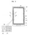
- FIG. 1is a schematic plan view of a display apparatus 1 , according to an example embodiment.
- FIG. 2is a schematic plan view of the display apparatus 1 , according to an example embodiment.
- the display apparatus 1may include a display substrate 20 provided with a display (or display area) DA, a sealing substrate 30 arranged to face (or overlap with) the display substrate 20 , and a sealing portion (or sealing area) SA bonding the display substrate 20 and the sealing substrate 30 together.
- the display apparatus 1may include a first metal line 310 which surrounds the display DA (e.g., circumferentially or around a periphery of the display DA) and a second metal line 320 , which is arranged to be spaced apart from the first metal line 310 .
- the display substrate 20may include a transparent glass material with Sio 2 as a main component.
- the material of the display substrate 20is not limited thereto, and the display substrate 20 may include various materials such as transparent plastic material or metal.
- the display DAmay be arranged on the display substrate 20 .
- an array of pixelsmay be formed, and the pixels may be controlled by thin film transistors, respectively.
- the display DAmay include a display device 210 .
- the display device 210may include a display device, which may produce an image by using an organic light-emitting diode (OLED) device, a liquid crystal display device, or an electrophoretic display device.
- OLEDorganic light-emitting diode
- pixels of the display DAmay include a thin film transistor and a liquid crystal layer which may be controlled by the thin film transistors respectively, and a backlight overlapping the display DA may be arranged.
- the sealing substrate 30may block external contaminants, moisture, or air from affecting the display device 210 , which is included in the display DA.
- a polarizing film or/and a color filtermay be further provided, depending on circumstances.
- the sealing portion SAis a portion by which the display substrate 20 and the sealing substrate 30 bind together.
- the sealing portion SAmay include a sealing member 300 and the first metal line 310 .
- a cutting area CMmay be a portion to be cut and divide an entire panel of display apparatuses into individual display apparatuses.
- the cutting area CMmay include the second metal line 320 , which may be arranged to be spaced apart from the first metal line 310 by a distance (e.g., a predetermined distance), and a connector 330 , which may connect the first metal line 310 and the second metal line 320 with each other.
- the sealing portion SAmay prevent or reduce instances of oxygen or moisture penetrating into the display DA and may improve mechanical strength of the display apparatus by bonding the display substrate 20 and the sealing substrate 30 together.
- the sealing portion SAmay be arranged to continuously surrounding the display DA (e.g., circumferentially or around a periphery of the display DA).
- the sealing portion SAmay be arranged continuously along or around an edge of the display substrate 20 and the sealing substrate 30 .
- the first metal line 310may be a metal layer arranged or formed below the sealing member 300 .
- the first metal line 310may transfer heat to the sealing member 300 by absorbing or/and reflecting a laser beam, the first metal line 310 may increase effective seal width or/and help harden the sealing member 300 evenly with just a low intensity of energy source.
- the effective seal widthmay refer to a width with which the sealing member 300 may connect the display substrate 20 to the sealing substrate 30 and block the flow of air and moisture after the sealing member 300 is melted and sintered again by absorbing heat energy.
- the second metal line 320may be a metal layer arranged to be spaced apart from the first metal line 310 by a distance (e.g., a predetermined distance).
- the second metal line 320may be arranged at an outer edge of the sealing portion SA.
- the outer edge of the sealing portion SAmay refer to an area which is far away (or furthest away) from the display DA.
- the first metal line 310may be formed continuously along the edge of the display DA while being arranged below the sealing portion SA.
- the second metal line 320may be arranged to be spaced apart from the first metal line 310 , and may be formed to surround the first metal line 310 around the edges of the display DA.
- the second metal line 320may include a 2 - 1 metal line 321 extending in a lengthwise direction of the display apparatus 1 and a 2 - 2 metal line 322 line extending in a widthwise direction of the display apparatus 1 .
- the 2 - 1 metal line 321 and the 2 - 2 metal line 322may be arranged alternately in a circumferential direction of the display apparatus 1 .
- the second metal line 320may be arranged to surround the first metal line 310 around the edges of the display DA.
- the connector 330is a connecting member, which may interconnect the first metal line 310 and the second metal line 320 with each other.
- the connector 330may be a metal layer, and may electrically connect the first metal line 310 and the second metal line 320 with each other while being arranged between the first metal line 310 and the second metal line 320 .
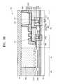
- FIG. 3Ais a partial cross-sectional view of the display apparatus 1 , cut along the line I-I′ shown in FIG. 2
- FIG. 3Bis a partial cross-sectional view of the display apparatus 1 , cut along the line II-II′ shown in FIG. 2
- the display apparatus 1will be described by using an OLED as an example, but is not limited thereto and may include any particular display apparatus, which produces an image by application of electricity thereto (e.g., a liquid crystal display device (LCD), a field emission display device (FED), or an electronic paper display device (EPD)).
- LCDliquid crystal display device
- FEDfield emission display device
- EPDelectronic paper display device
- the display apparatus 1may include the display DA displaying an image, the sealing portion SA sealing the display DA, and the cutting area CM to be cut and divide the entire panel of display apparatuses into individual display apparatuses.
- the display substrate 20may further include a buffer layer 211 .
- the buffer layer 211may prevent an impurity ion from proliferating on a top surface of the display substrate 20 and keep moisture or external air from infiltrating the display substrate 20 , and planarize a surface of the display substrate 20 .
- the buffer layer 211may be omitted.
- the buffer layer 211may be formed by using various methods such as a plasma-enhanced chemical vapor deposition (PECVD), an atmospheric pressure CVD (APCVD), or a low pressure CVD (LPCVD).
- PECVDplasma-enhanced chemical vapor deposition
- APCVDatmospheric pressure CVD
- LPCVDlow pressure CVD
- the display DAmay be provided with the display device 210 which produces an image, as shown in FIG. 1 .
- the display device 210may be an OLED, an LCD, or an electrophoretic display device.
- the display device 210may be an OLED display device, as an example.
- a first thin film transistor TFT 1 and a second thin film transistor TFT 2may each include an activation layer 212 , a gate electrode 214 , a source electrode 216 and a drain electrode 217 .
- a first gate insulation film 213 a for insulating the gate electrode 214 and the activation layer 212 from each othermay be between the gate electrode 214 and the activation layer 212 .
- the gate electrode 214may overlap a part of the activation layer 212 on the first gate insulation film 213 a .
- the first thin film transistor TFT 1may be arranged or formed below the OLED, and may be a driving thin film transistor for driving the OLED.
- the activation layer 212may be arranged on the buffer layer 211 .
- the activation layer 212may include an inorganic semiconductor such as amorphous silicon or polysilicon or an organic semiconductor.
- a first gate insulation film 213 amay be provided on the buffer layer 211 , covering the activation layer 212 .
- a second gate insulation film 213 bmay be formed on the first gate insulation film 213 a and covers the gate electrode 214 .
- the gate electrode 214may include a single layer or layers including Au, Ag, Cu, Ni, Pt, Pd, Al, Mo, Cr, an alloy of Al and Nd or an alloy of Mo and W.
- the first gate insulation film 213 a and the second gate insulation film 213 bmay include an inorganic film such as silicon oxide, silicon nitride, and metal oxide, and such film may include a single layer or layers.
- An interlayer insulation film 215may be formed on the second gate insulation film 213 b .
- the interlayer insulation film 215may include an inorganic film such as silicon oxide and silicon nitride.
- the interlayer insulation film 215may include an organic film.
- the source electrode 216 and the drain electrode 217may be formed on the interlayer insulation film 215 . Each of the source electrode 216 and the drain electrode 217 may contact the activation layer 212 through a contact hole.
- the source electrode 216 and the drain electrode 217may include a metal, an alloy, a metal nitride, a conductive metal oxide, or a transparent conductive material.
- a structure of the thin film transistoris not limited thereto, and other thin film transistor structures may be possible.
- the thin film transistormay be a top gate transistor, or a bottom gate transistor with the gate electrode 214 below the activation layer 212 .
- a capacitor 230may be included in the display DA.
- the capacitor 230may store a data signal supplied to the display device 210 or compensate for a voltage drop of the display device 210 .
- the capacitor 230may include a first capacitor electrode 230 A, a second capacitor electrode 230 B, and the second gate insulation film 213 b therebetween.
- the first and second capacitor electrode 230 A and 230 Bmay include the same material as the gate electrode 214 .
- a planarizing film 218may be arranged on the interlayer insulation film 215 while covering the first and second thin film transistors TFT 1 and TFT 2 and the capacitor 230 .
- the planarizing film 218may eliminate a step of a layer therebelow and planarize the surface of the layer therebelow so as to increase a light-emitting efficiency of the OLED, which is arranged on the planarizing film 218 .
- the planarizing film 218may have a penetration hole which exposes a portion of the drain electrode 217 .
- embodiments of the present inventionare not limited to the structure previously described, and according to some example embodiments, either one of the planarizing film 218 and the interlayer insulation film 215 may be omitted, depending on circumstances.
- the OLEDmay be arranged on the planarizing film 218 , and may include a first electrode 221 , an intermediate layer 220 including an organic light-emitting layer, and a second electrode 222 .
- a pixel-defining film 219may be arranged on the planarizing film 218 and cover a portion of the first electrode 221 , and may define a pixel area and a non-pixel area.
- a hole and an electron injected at the first electrode 221 and the second electrode 222 of the OLEDmay combine with the organic light-emitting layer of the intermediate layer 220 to produce light.
- the intermediate layer 220may include the organic light-emitting layer.
- the intermediate layer 220may include the organic light-emitting layer and may further include at least one of a hole injection layer (HIL), a hole transport layer (HTL), an electron transport layer (ETL), and an electron injection layer (EIL).
- HILhole injection layer
- HTLhole transport layer
- ETLelectron transport layer
- EILelectron injection layer
- the present inventionis not limited thereto, and the intermediate layer 220 may include the organic light-emitting layer and may further include other various functional layers.
- the second electrode 222may be formed on the intermediate layer 220 .
- the second electrode 222may form an electric field with the first electrode 221 to enable the intermediate layer 220 to emit light.
- the first electrode 221may be patterned in each pixel, and the second electrode 222 may be formed so as to have a common voltage applied to all pixels.
- the second electrode 222may be electrically connected through a power wiring 240 and a circuit wiring 241 which are provided at the edges of the display 22 .
- the first electrode 221 and the second electrode 222may include a transparent electrode or a reflective electrode.
- the first electrode 221may function as an anode electrode while the second electrode 222 may function as a cathode electrode, but not limited thereto.
- the first electrode 221may function as a cathode electrode while the second electrode 222 may function as an anode electrode.
- the display DAmay include a plurality of the OLEDs.
- a pixelmay be formed for each OLED, and each pixel may produce red, green, blue or white color.
- a protective layermay be formed on the second electrode 222 and may cover and protect the OLED.
- the protective layermay use an inorganic insulation film and/or an organic insulation film.
- a spacer 223may be arranged between the display substrate 20 and the sealing substrate 30 and keep a distance between the display substrate 20 and the sealing substrate 30 .
- the spacer 223may be arranged to prevent a reduction in display capacity of the display apparatus 1 due to an external shock.
- the spacer 223may be arranged on the pixel-defining film 219 .
- the spacer 223may be arranged while protruding toward the sealing substrate 30 from the pixel-defining film 219 .
- the second electrode 222 and/or the protective layermay be arranged on the spacer 223 .
- the sealing substrate 30may be provided as a transparent component, as previously described. Accordingly, it is possible to have an image produced on the display device exposed externally through the sealing substrate 30 .
- the sealing member 300may be arranged to surround the display device 210 between the display substrate 20 and the sealing substrate 30 , and may seal a space between the display substrate 20 and the sealing substrate 30 .
- the sealing member 300may be an inorganic material.
- the sealing member 300may be a glass frit, and the glass frit may be applied over the sealing member 300 by using a dispenser or a screen printing method.
- glass fritrefers to a glass ingredient in the form of powder, but the present invention is not limited thereto.
- glass fritmay include a paste including not only such main material as SiO2 but also a laser or an infrared absorbing material, an organic binder, and a filler for reducing thermal expansion coefficient. The laser beam is irradiated to the sealing member 300 , which in turn melts and hardens the sealing member 300 to bond the display substrate 20 and the sealing substrate 30 together.
- the sealing member 300e.g., glass frit
- a thicknesse.g., a predetermined thickness
- the sealing substrate 30by aligning the sealing substrate 30 above the display substrate 20 , putting them into a vacuum sintering furnace, and heating just the glass frit-applied portion surgically (e.g., with precision) with the laser beam while heating them at an appropriate temperature below the melting point of the glass frit, it may possible to melt the glass frit and bond the display substrate 20 and the sealing substrate 30 together.
- the laser-assisted vacuum packaging methodwhen the laser beam is irradiated onto the sealing member 300 and the sealing member 300 melts, a relatively large number of air bubbles may occur.
- the area where sources of air bubbles such as moisture or binder ingredients are removed sufficientlymay be 30 ⁇ m-40 ⁇ m away from the surface of the sealing member 300 .
- the sources of air bubblesremain without being removed sufficiently in the inside of the sealing member 300 , a relatively large number of air bubbles may occur when the sealing member 300 melts.
- a pin-hole which has been trapped inside the sealing member 300may expand in a vacuum sintering furnace due to a difference in pressure, or a small amount of binder ingredients which have still remained without being removed in the phase of the pre-calcination burn, and thus air bubbles may be generated by gas.
- air bubbles, which occurred at the sealing member 300are placed at a bonding surface of the display substrate and sealing substrate 20 and 30 , and the sealing member 300 , it may reduce an effective contact area of the display substrate and sealing substrate 20 and 30 and the sealing member 300 , which may result in a decrease in adhesive strength of the sealing member 300 .
- air bubbles occurring inside the sealing member 300may be placed mainly at an area between display substrate 20 and the sealing member 300 , e.g., the space below the sealing member 300 where air bubbles have not been sufficiently removed. Accordingly, by removing air bubbles at the area between a top surface of the display substrate 20 and a bottom surface of the sealing member 300 or by expelling air bubbles upwardly to the top surface of the sealing member 300 , it may be possible to prevent a reduction in the effective contact area between the display substrate 20 and the sealing member 300 .
- the first metal line 310is a metal layer which is arranged below the sealing member 300 , and may transfer heat to the space below the sealing member 300 by absorbing or/and reflecting laser light. Accordingly, by removing air bubbles or expelling air bubbles upwardly to the top surface of the sealing member 300 , it may be possible to prevent a reduction in the effective contact area of the display substrate 20 and the sealing member 300 .
- the first metal line 310may be formed to have the same width as that of the sealing member 300 and a uniform thickness so as to produce uniform heat energy all over the first metal line 310 .
- the first metal line 310may apply uniform heat amount all over the sealing member 300 , by being present or positioned below the sealing member 300 .
- the present inventionis not limited thereto, and the width and a placement of the first metal line 310 may vary according to a shape and a number of the air bubbles placed at the space below the sealing member 300 , so as to apply the heat amount exclusively to a part of the bottom of the sealing member 300 .
- One or more first metal lines 310may be provided depending on a location to which the heat is applied.
- the first metal line 310may include a conductive material or metal with resistance, an alloy or a combination of both so as to produce heat when an electric current goes through the first metal line 310 .
- the first metal line 310may be formed on the same layer as any one of the gate electrode 214 , the source electrode 216 , the drain electrode 217 or the first and second capacitor electrodes 230 A and 230 B.
- the first metal line 310may include the same material as any one of the gate electrode 214 , the source electrode 216 , the drain electrode 217 or the first and second capacitor electrodes 230 A and 230 B (e.g., a single layer or a plurality of layers including, for example, Au, Ag, Cu, Ni, Pt, Pd, Al, Mo, Cr, an alloy of Al and Nd or an alloy of Mo and W).
- the first metal line 310may be arranged below the sealing member 300 in a lengthwise direction of the sealing member 300 .
- the first metal line 310may be arranged between the second gate insulation film 213 b and the interlayer insulation film 215 , and may be extended in a lengthwise direction of the sealing portion SA in which the sealing member 300 is placed.
- the first metal line 310may be arranged at any location (e.g., any random location) between the sealing member 300 and the display substrate 20 (e.g., between the second gate insulation film 213 b and the sealing member 300 ).
- the second metal line 320may be arranged to be spaced apart from the first metal line 310 by a distance (e.g., a predetermined distance) so as to be electrically connected to the first metal line 310 . Accordingly, by reducing resistance which occurs from the first metal line 310 , it may be possible to prevent or reduce instances of a delamination, which may be caused by an electrostatic discharge (ESD) of the sealing member 300 and the display substrate 20 .
- ESDelectrostatic discharge
- the second metal line 320may be arranged to be spaced apart from the first metal line 310 so as to be formed surrounding the first metal line 310 .
- the second metal line 320may include the 2 - 1 metal line 321 (i.e., a first portion of the second metal line 320 ) extending in a lengthwise direction of the display DA and the 2 - 2 metal line 322 (i.e., a second portion of the second metal line 320 ) extending in a widthwise direction of the display DA.
- the 2 - 1 metal line 321 and the 2 - 2 metal line 322may be arranged alternately along a circumferential direction (or around the periphery) of display DA.
- the second metal line 320may be arranged so as to surround the first metal line 310 .
- the 2 - 1 metal line 321 and the 2 - 2 metal line 322may be arranged to be spaced apart as shown in FIG. 2 , but the present invention is not limited thereto.
- the second metal line 320may be formed continuously so as to surround the first metal line 310 .
- the second metal line 320may be formed to include a width (e.g., a predetermined width) (e.g., a width of more than 50 ⁇ m) so as to reduce resistance that may be caused from the first metal line 310 .
- a widthe.g., a predetermined width
- a width of more than 50 ⁇ me.g., a width of more than 50 ⁇ m
- the second metal line 320may include a conductive material or metal with resistance, an alloy or a combination of both. In an example embodiment, the second metal line 320 may be formed on the same layer as any one of the gate electrode 214 , the source electrode 216 , the drain electrode 217 or the first and second capacitor electrodes 230 A and 230 B.
- the second metal line 320may include the same material as any one of the gate electrode 214 , the source electrode 216 , the drain electrode 217 or the first and second capacitor electrodes 230 A and 230 B (e.g., a single-layer film or multi-layer film including Au, Ag, Cu, Ni, Pt, Pd, Al, Mo, Cr, an alloy of Al and Nd or an alloy of Mo and W).
- the second metal line 320may include either a same material as that of the first metal line 310 or of a different material from that of the first metal line 310 .
- the second metal line 320may be arranged on the same layer as the first metal line 310 .
- the second metal line 320may be arranged to be spaced apart from the first metal line 310 by a distance (e.g., a predetermined distance) between the second gate insulation film 213 b and the interlayer insulation film 215 .
- a distancee.g., a predetermined distance
- embodiments of the present inventionare not limited thereto, and the second metal line 320 may be arranged on a different layer from the first metal line 310 .
- the second metal line 320may be arranged between the first gate insulation film 213 a and the second gate insulation film 213 b.
- the connector 330is the connecting member that may be arranged between the first metal line 310 and the second metal line 320 to electrically connect the first metal line 310 and the second metal line 320 with each other.
- the connector 330may include the same material as that of the first metal line 310 or the second metal line 320 (e.g., the single-layer film or the multi-layer film including Au, Ag, Cu, Ni, Pt, Pd, Al, Mo, Cr, an alloy of Al and Nd or an alloy of Mo and W).
- the first metal line 310 and the second metal line 320 , and the connector 330will be described in more detail hereinafter, by referring to the figures.
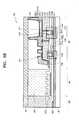
- FIG. 4is a partial cross-sectional view of the display apparatus 1 , cut along a lengthwise direction thereof, according to an example embodiment.
- FIG. 5is a partial cross-sectional view of the display apparatus 1 , cut along a lengthwise direction thereof, according to another example embodiment.
- the connector 330may connect the first metal line 310 , the 2 - 1 metal line 321 and the 2 - 2 metal line 322 , respectively.
- the connector 330will be described by focusing on the connector 330 which connects the first metal line 310 and the 2 - 1 metal line 321 for the convenience of explanation.
- the first metal line 310 and the 2 - 1 metal line 321may be arranged to be spaced apart by a distance (e.g., a predetermined distance) (e.g., a first distance T) and the connector 330 may be arranged between the first metal line 310 and the 2 - 1 metal line 321 so as to connect the first metal line 310 and the 2 - 1 metal line 321 .
- a distancee.g., a predetermined distance
- the connector 330may be arranged between the first metal line 310 and the 2 - 1 metal line 321 so as to connect the first metal line 310 and the 2 - 1 metal line 321 .
- the first distance Tmay be 30 ⁇ m or more.
- the connector 330may include a plurality of the connecting members 331 through 335 , and the connecting members 331 through 335 may be arranged to be spaced apart from one another by a distance (e.g., a predetermined distance) (e.g., a second distance M) along a lengthwise direction of the display DA.
- a distancee.g., a predetermined distance
- a second distance Me.g., a second distance M
- a first connecting member 331 and a second connecting member 332may be arranged to be spaced apart by a 2 - 1 distance M 1
- a second connecting member 332 and a third connecting member 333may be arranged to be spaced apart by a 2 - 2 distance M 2 .
- the 2 - 1 distance M 1 and the 2 - 2 distance M 2may be formed identically (or substantially identically) or differently.
- the connector 330may include the third and fourth connecting members 330 A and 330 B, and may be arranged at both ends of the 2 - 1 metal line 321 so as to be spaced apart.
- a width D 2 of the third and fourth connecting members 330 A and 330 Bmay be formed to be larger than a width D 1 of the first connecting member 331 as shown in FIG. 4 , but example embodiments of the present invention are not limited thereto.
- FIG. 6Ais a partial cross-sectional view of the display apparatus 1 , cut along the line I-I′ shown in FIG. 2 , according to another example embodiment.
- FIG. 6Bis a partial cross-sectional view of the display apparatus 1 , cut along the line II′ shown in FIG. 2 , according to another example embodiment.
- descriptions of essentially identical configurations as those described in FIGS. 3A and 3Bmay be omitted.
- the first metal line 310 and the second metal line 320may be arranged on the same layer or on different layers between the sealing member 300 and the display substrate 20 .
- the first metal line 310may be arranged between the second gate insulation film 213 b and the interlayer insulation film 215 .
- the second metal line 320may be arranged between the first gate insulation film 213 a and the second gate insulation film 213 b .
- example embodiments of the present inventionare not limited thereto, and the first metal line 310 and the second metal line 320 may be arranged on any different layers provided between the sealing member 300 and the display substrate 20 .
- the first metal line 310 and the second metal line 320may be electrically connected.
- the contact hole Hmay be formed on a portion of the second gate insulation film 213 b .
- the first metal line 310 and the second metal line 320may be electrically connected, as the first metal line 310 contacts the second metal line 320 by using the contact hole H.
- the display apparatus 1may improve the delamination which may be caused by the ESD and cutting defects of the substrate simultaneously, by including the first metal line 310 provided below the sealing member 300 and the second metal line 320 , which is arranged to be spaced apart from the first metal line 310 .
Landscapes
- Physics & Mathematics (AREA)
- Microelectronics & Electronic Packaging (AREA)
- Engineering & Computer Science (AREA)
- Optics & Photonics (AREA)
- Nonlinear Science (AREA)
- Geometry (AREA)
- Mathematical Physics (AREA)
- General Physics & Mathematics (AREA)
- Crystallography & Structural Chemistry (AREA)
- Chemical & Material Sciences (AREA)
- Electroluminescent Light Sources (AREA)
- Devices For Indicating Variable Information By Combining Individual Elements (AREA)
- Electromagnetism (AREA)
- Display Devices Of Pinball Game Machines (AREA)
- Electrochromic Elements, Electrophoresis, Or Variable Reflection Or Absorption Elements (AREA)
Abstract
Description
- This application claims priority to and the benefit of Korean Patent Application No. 10-2015-0140616, filed on Oct. 6, 2015, in the Korean Intellectual Property Office, the disclosure of which is incorporated herein in its entirety by reference.
- 1. Field
- Aspects of one or more example embodiments of the present invention relate to a display apparatus.
- 2. Description of the Related Art
- Generally, display apparatuses such as an organic light-emitting display (OLED) apparatus or a liquid-crystal display (LCD) apparatus including a thin film transistor (TFT) are popular to utilize as display apparatuses for various types of mobile devices such as digital cameras, video cameras, camcorders, portable information terminals, or smartphones.
- Such display apparatuses may utilize sealing to protect internal components of the display device from external contaminants. For example, a plurality of substrates utilized in a display apparatus may be bonded together, through a method of applying sealing material between the substrates and hardening the sealing material using any suitable method, such as by irradiating a laser beam thereto from a laser.
- A metal line may be arranged below the sealing material in order to increase adhesion of an upper substrate to a lower substrate. As the width of the metal line arranged below the sealing material expands, the sealing material may be unevenly formed, however, which in turn may increase a risk of cutting defects of a substrate.
- It is to be understood that this Background section is intended to provide useful background for understanding the technology and as such, the Background section of the present disclosure may include ideas, concepts, or recognitions that do not constitute prior art.
- Additional aspects will be set forth in part in the description which follows and, in part, will be apparent from the description, or may be learned by practice of the following example embodiments.
- According to one or more example embodiments of the present invention, a display apparatus includes: a display substrate; a display on the display substrate, the display comprising a display device; a sealing substrate on the display substrate; a sealing member bonding the display substrate and the sealing substrate, the sealing member surrounding the display; a first metal line below the sealing member and surrounding the display; a second metal line on the display substrate and spaced apart from the first metal line; and one or more connectors connecting the first metal line and the second metal line with each other.
- According to some embodiments, the second metal line includes a first portion extending in a lengthwise direction of the display and a second portion extending in a widthwise direction of the display.
- According to some embodiments, the display apparatus further includes two or more connectors connecting the first metal line to the second metal line, wherein the two or more connectors are provided at both ends of each of the first portion and the second portion of the second metal line.
- According to some embodiments, the two or more connectors are spaced apart from one another by a first distance along the lengthwise direction of the display between the first portion of the second metal line and the first metal line, and spaced apart from one another by a second distance along the widthwise direction of the display between the second portion of the second metal line and the first metal line.
- According to some embodiments, first distance is equal to the second distance.
- According to some embodiments, first distance is different from the second distance.
- According to some embodiments, the display includes a thin film transistor comprising a gate electrode, a source electrode, and a drain electrode, and a capacitor including a plurality of capacitor electrodes; and the first metal line and the second metal line are on a same layer as any one of the gate electrode, the source electrode, the drain electrode, and the plurality of capacitor electrodes.
- According to some embodiments, the first metal line and the second metal line include a same material as a material in any one of the gate electrode, the source electrode, the drain electrode, and the plurality of capacitor electrodes.
- According to some embodiments, the display apparatus further includes a plurality of insulating layers between the display substrate and the sealing member, wherein the first metal line and the second metal line are between the plurality of insulating layers and the sealing member.
- According to some embodiments, the first metal line and the second metal line are at different layers.
- According to some embodiments, the first metal line and the second metal line are at a same layer.
- According to some embodiments, the first metal line is spaced from the second metal line by 30 μm or more.
- According to some embodiments, the sealing member includes glass frit.
- According to some embodiments, the display device is an organic light-emitting device including a first electrode, an intermediate layer comprising an organic light-emitting layer, and a second electrode consecutively stacked on one another, respectively.
- These and/or other aspects and features of example embodiments of the present invention will become more apparent and more readily appreciated from the following description of the example embodiments, taken in conjunction with the accompanying drawings in which:
FIG. 1 is a schematic plan view of a display apparatus, according to some example embodiments of the present invention;FIG. 2 is a schematic plan view of the display apparatus, according to some example embodiments of the present invention;FIG. 3A is a partial cross-sectional view of the display apparatus, cut along the line I-I′ shown inFIG. 2 ;FIG. 3B is a partial cross-sectional view of the display apparatus, cut along the line II-II′ shown inFIG. 2 FIG. 4 is a partial cross-sectional view of the display apparatus, cut along a lengthwise direction, according to some example embodiments of the present invention;FIG. 5 is a partial cross-sectional view of the display apparatus, cut along a lengthwise direction, according to some example embodiments of the present invention;FIG. 6A is a partial cross-sectional view of the display apparatus, cut along the line I-I′ shown inFIG. 2 , according to some example embodiments of the present invention; andFIG. 6B is a partial cross-sectional view of the display apparatus, cut along the line II-II′ shown inFIG. 2 , according to some example embodiments of the present invention.- As the invention allows for various changes and numerous embodiments, example embodiments will be illustrated in the drawings and described in more detail in the written description. Aspects and features of the present invention and ways to achieve those will become more clearly understood, when referring to example embodiments described later in more detail with drawings. This invention may, however, be embodied in many different forms and should not be construed as limited to the example embodiments set forth herein.
- Hereinafter, aspects of example embodiments of the present invention will be described in more detail by explaining example embodiments of the present invention with reference to the attached drawings. In explaining example embodiments of the present invention by referring to the drawings, the same reference numerals will be given to virtually the same or corresponding components, and some redundant explanation may be omitted.
- It will be understood that although the terms “first,” “second,” etc. may be used herein to describe various components, these components should not be limited by these terms. These components are only used to distinguish one component from another. Thus, a first element, component, region, layer or section described below could be termed a second element, component, region, layer or section, without departing from the spirit and scope of the present invention.
- As used herein, the singular forms “a,” “an” and “the” are intended to include the plural forms as well, unless the context clearly indicates otherwise.
- It will be understood that the terms “comprises” and/or “comprising” used herein specify the presence of stated features or components, but do not preclude the presence or addition of one or more other features or components.
- It will be further understood that when a layer, region, or component is referred to as being “formed on” another layer, region, or component, it can be directly or indirectly formed on the other layer, region, or component. That is, for example, intervening layers, regions, or components may be present, unless stated otherwise.
- In the drawings, sizes of components may be magnified or minimized for the convenience of explanation. For example, as size and thickness of each component shown in the drawings may be presented arbitrarily for the convenience of explanation, the present invention is not limited thereto.
- Spatially relative terms, such as “beneath,” “below,” “lower,” “under,” “above,” “upper,” and the like, may be used herein for ease of explanation to describe one element or feature's relationship to another element(s) or feature(s) as illustrated in the figures. It will be understood that the spatially relative terms are intended to encompass different orientations of the device in use or in operation, in addition to the orientation depicted in the figures. For example, if the device in the figures is turned over, elements described as “below” or “beneath” or “under” other elements or features would then be oriented “above” the other elements or features. Thus, the example terms “below” and “under” can encompass both an orientation of above and below. The device may be otherwise oriented (e.g., rotated 90 degrees or at other orientations) and the spatially relative descriptors used herein should be interpreted accordingly.
- It will be understood that when an element or layer is referred to as being “on,” “connected to,” or “coupled to” another element or layer, it can be directly on, connected to, or coupled to the other element or layer, or one or more intervening elements or layers may be present. In addition, it will also be understood that when an element or layer is referred to as being “between” two elements or layers, it can be the only element or layer between the two elements or layers, or one or more intervening elements or layers may also be present.
- As used herein, the term “substantially,” “about,” and similar terms are used as terms of approximation and not as terms of degree, and are intended to account for the inherent deviations in measured or calculated values that would be recognized by those of ordinary skill in the art. Further, the use of “may” when describing embodiments of the present invention refers to “one or more embodiments of the present invention.” As used herein, the terms “use,” “using,” and “used” may be considered synonymous with the terms “utilize,” “utilizing,” and “utilized,” respectively. Also, the term “exemplary” is intended to refer to an example or illustration.
- Unless otherwise defined, all terms (including technical and scientific terms) used herein have the same meaning as commonly understood by one of ordinary skill in the art to which the present invention belongs. It will be further understood that terms, such as those defined in commonly used dictionaries, should be interpreted as having a meaning that is consistent with their meaning in the context of the relevant art and/or the present specification, and should not be interpreted in an idealized or overly formal sense, unless expressly so defined herein.
FIG. 1 is a schematic plan view of adisplay apparatus 1, according to an example embodiment.FIG. 2 is a schematic plan view of thedisplay apparatus 1, according to an example embodiment.- Referring to
FIGS. 1 and 2 , thedisplay apparatus 1, according to an example embodiment, may include adisplay substrate 20 provided with a display (or display area) DA, a sealingsubstrate 30 arranged to face (or overlap with) thedisplay substrate 20, and a sealing portion (or sealing area) SA bonding thedisplay substrate 20 and the sealingsubstrate 30 together. In some embodiments, below the sealing portion SA, thedisplay apparatus 1 may include afirst metal line 310 which surrounds the display DA (e.g., circumferentially or around a periphery of the display DA) and asecond metal line 320, which is arranged to be spaced apart from thefirst metal line 310. - The
display substrate 20 may include a transparent glass material with Sio2as a main component. However, the material of thedisplay substrate 20 is not limited thereto, and thedisplay substrate 20 may include various materials such as transparent plastic material or metal. - The display DA may be arranged on the
display substrate 20. On the display DA, an array of pixels may be formed, and the pixels may be controlled by thin film transistors, respectively. The display DA may include adisplay device 210. In some embodiments, thedisplay device 210 may include a display device, which may produce an image by using an organic light-emitting diode (OLED) device, a liquid crystal display device, or an electrophoretic display device. In some embodiments, pixels of the display DA may include a thin film transistor and a liquid crystal layer which may be controlled by the thin film transistors respectively, and a backlight overlapping the display DA may be arranged. - The sealing
substrate 30 may block external contaminants, moisture, or air from affecting thedisplay device 210, which is included in the display DA. On the sealingsubstrate 30, a polarizing film or/and a color filter may be further provided, depending on circumstances. - The sealing portion SA is a portion by which the
display substrate 20 and the sealingsubstrate 30 bind together. The sealing portion SA may include a sealingmember 300 and thefirst metal line 310. A cutting area CM may be a portion to be cut and divide an entire panel of display apparatuses into individual display apparatuses. The cutting area CM may include thesecond metal line 320, which may be arranged to be spaced apart from thefirst metal line 310 by a distance (e.g., a predetermined distance), and aconnector 330, which may connect thefirst metal line 310 and thesecond metal line 320 with each other. - The sealing portion SA may prevent or reduce instances of oxygen or moisture penetrating into the display DA and may improve mechanical strength of the display apparatus by bonding the
display substrate 20 and the sealingsubstrate 30 together. In an example embodiment, the sealing portion SA may be arranged to continuously surrounding the display DA (e.g., circumferentially or around a periphery of the display DA). For example, the sealing portion SA may be arranged continuously along or around an edge of thedisplay substrate 20 and the sealingsubstrate 30. - The
first metal line 310 may be a metal layer arranged or formed below the sealingmember 300. As thefirst metal line 310 may transfer heat to the sealingmember 300 by absorbing or/and reflecting a laser beam, thefirst metal line 310 may increase effective seal width or/and help harden the sealingmember 300 evenly with just a low intensity of energy source. In this case, the effective seal width may refer to a width with which the sealingmember 300 may connect thedisplay substrate 20 to the sealingsubstrate 30 and block the flow of air and moisture after the sealingmember 300 is melted and sintered again by absorbing heat energy. - The
second metal line 320 may be a metal layer arranged to be spaced apart from thefirst metal line 310 by a distance (e.g., a predetermined distance). Thesecond metal line 320 may be arranged at an outer edge of the sealing portion SA. In this case, the outer edge of the sealing portion SA may refer to an area which is far away (or furthest away) from the display DA. - From a different perspective, the
first metal line 310 may be formed continuously along the edge of the display DA while being arranged below the sealing portion SA. In this case, thesecond metal line 320 may be arranged to be spaced apart from thefirst metal line 310, and may be formed to surround thefirst metal line 310 around the edges of the display DA. - In an example embodiment, the
second metal line 320 may include a2-1metal line 321 extending in a lengthwise direction of thedisplay apparatus 1 and a2-2metal line 322 line extending in a widthwise direction of thedisplay apparatus 1. In this case, the2-1metal line 321 and the2-2metal line 322 may be arranged alternately in a circumferential direction of thedisplay apparatus 1. Accordingly, thesecond metal line 320 may be arranged to surround thefirst metal line 310 around the edges of the display DA. - The
connector 330 is a connecting member, which may interconnect thefirst metal line 310 and thesecond metal line 320 with each other. Theconnector 330 may be a metal layer, and may electrically connect thefirst metal line 310 and thesecond metal line 320 with each other while being arranged between thefirst metal line 310 and thesecond metal line 320. FIG. 3A is a partial cross-sectional view of thedisplay apparatus 1, cut along the line I-I′ shown inFIG. 2 , andFIG. 3B is a partial cross-sectional view of thedisplay apparatus 1, cut along the line II-II′ shown inFIG. 2 . In the present embodiment, thedisplay apparatus 1 will be described by using an OLED as an example, but is not limited thereto and may include any particular display apparatus, which produces an image by application of electricity thereto (e.g., a liquid crystal display device (LCD), a field emission display device (FED), or an electronic paper display device (EPD)).- Referring to
FIGS. 3A and 3B , thedisplay apparatus 1 may include the display DA displaying an image, the sealing portion SA sealing the display DA, and the cutting area CM to be cut and divide the entire panel of display apparatuses into individual display apparatuses. - The
display substrate 20 may further include abuffer layer 211. Thebuffer layer 211 may prevent an impurity ion from proliferating on a top surface of thedisplay substrate 20 and keep moisture or external air from infiltrating thedisplay substrate 20, and planarize a surface of thedisplay substrate 20. According to some example embodiments, thebuffer layer 211 may be omitted. Thebuffer layer 211 may be formed by using various methods such as a plasma-enhanced chemical vapor deposition (PECVD), an atmospheric pressure CVD (APCVD), or a low pressure CVD (LPCVD). - The display DA may be provided with the
display device 210 which produces an image, as shown inFIG. 1 . As previously described in some detail, thedisplay device 210 may be an OLED, an LCD, or an electrophoretic display device. However, according to some embodiments, thedisplay device 210 may be an OLED display device, as an example. - A first thin film transistor TFT1 and a second thin film transistor TFT2 may each include an
activation layer 212, agate electrode 214, asource electrode 216 and adrain electrode 217. A firstgate insulation film 213afor insulating thegate electrode 214 and theactivation layer 212 from each other may be between thegate electrode 214 and theactivation layer 212. Thegate electrode 214 may overlap a part of theactivation layer 212 on the firstgate insulation film 213a. The first thin film transistor TFT1 may be arranged or formed below the OLED, and may be a driving thin film transistor for driving the OLED. - The
activation layer 212 may be arranged on thebuffer layer 211. Theactivation layer 212 may include an inorganic semiconductor such as amorphous silicon or polysilicon or an organic semiconductor. - A first
gate insulation film 213amay be provided on thebuffer layer 211, covering theactivation layer 212. A secondgate insulation film 213bmay be formed on the firstgate insulation film 213aand covers thegate electrode 214. - The
gate electrode 214 may include a single layer or layers including Au, Ag, Cu, Ni, Pt, Pd, Al, Mo, Cr, an alloy of Al and Nd or an alloy of Mo and W. - The first
gate insulation film 213aand the secondgate insulation film 213bmay include an inorganic film such as silicon oxide, silicon nitride, and metal oxide, and such film may include a single layer or layers. - An
interlayer insulation film 215 may be formed on the secondgate insulation film 213b. Theinterlayer insulation film 215 may include an inorganic film such as silicon oxide and silicon nitride. Theinterlayer insulation film 215 may include an organic film. - The
source electrode 216 and thedrain electrode 217 may be formed on theinterlayer insulation film 215. Each of thesource electrode 216 and thedrain electrode 217 may contact theactivation layer 212 through a contact hole. Thesource electrode 216 and thedrain electrode 217 may include a metal, an alloy, a metal nitride, a conductive metal oxide, or a transparent conductive material. - A structure of the thin film transistor is not limited thereto, and other thin film transistor structures may be possible. For example, the thin film transistor may be a top gate transistor, or a bottom gate transistor with the
gate electrode 214 below theactivation layer 212. - A
capacitor 230 may be included in the display DA. Thecapacitor 230 may store a data signal supplied to thedisplay device 210 or compensate for a voltage drop of thedisplay device 210. - The
capacitor 230 may include a first capacitor electrode230A, a second capacitor electrode230B, and the secondgate insulation film 213btherebetween. The first and second capacitor electrode230A and230B may include the same material as thegate electrode 214. - A
planarizing film 218 may be arranged on theinterlayer insulation film 215 while covering the first and second thin film transistors TFT1 and TFT2 and thecapacitor 230. Theplanarizing film 218 may eliminate a step of a layer therebelow and planarize the surface of the layer therebelow so as to increase a light-emitting efficiency of the OLED, which is arranged on theplanarizing film 218. In some embodiments, theplanarizing film 218 may have a penetration hole which exposes a portion of thedrain electrode 217. - However, embodiments of the present invention are not limited to the structure previously described, and according to some example embodiments, either one of the
planarizing film 218 and theinterlayer insulation film 215 may be omitted, depending on circumstances. - The OLED may be arranged on the
planarizing film 218, and may include afirst electrode 221, anintermediate layer 220 including an organic light-emitting layer, and asecond electrode 222. A pixel-definingfilm 219 may be arranged on theplanarizing film 218 and cover a portion of thefirst electrode 221, and may define a pixel area and a non-pixel area. - A hole and an electron injected at the
first electrode 221 and thesecond electrode 222 of the OLED may combine with the organic light-emitting layer of theintermediate layer 220 to produce light. - The
intermediate layer 220 may include the organic light-emitting layer. In another example embodiment, theintermediate layer 220 may include the organic light-emitting layer and may further include at least one of a hole injection layer (HIL), a hole transport layer (HTL), an electron transport layer (ETL), and an electron injection layer (EIL). However, the present invention is not limited thereto, and theintermediate layer 220 may include the organic light-emitting layer and may further include other various functional layers. - The
second electrode 222 may be formed on theintermediate layer 220. Thesecond electrode 222 may form an electric field with thefirst electrode 221 to enable theintermediate layer 220 to emit light. Thefirst electrode 221 may be patterned in each pixel, and thesecond electrode 222 may be formed so as to have a common voltage applied to all pixels. Thesecond electrode 222 may be electrically connected through apower wiring 240 and acircuit wiring 241 which are provided at the edges of the display22. - The
first electrode 221 and thesecond electrode 222 may include a transparent electrode or a reflective electrode. Thefirst electrode 221 may function as an anode electrode while thesecond electrode 222 may function as a cathode electrode, but not limited thereto. For example, thefirst electrode 221 may function as a cathode electrode while thesecond electrode 222 may function as an anode electrode. - Although the drawings of the present invention only show just one OLED, the display DA may include a plurality of the OLEDs. A pixel may be formed for each OLED, and each pixel may produce red, green, blue or white color.
- A protective layer may be formed on the
second electrode 222 and may cover and protect the OLED. The protective layer may use an inorganic insulation film and/or an organic insulation film. - A
spacer 223 may be arranged between thedisplay substrate 20 and the sealingsubstrate 30 and keep a distance between thedisplay substrate 20 and the sealingsubstrate 30. Thespacer 223 may be arranged to prevent a reduction in display capacity of thedisplay apparatus 1 due to an external shock. - In some embodiments, the
spacer 223 may be arranged on the pixel-definingfilm 219. Thespacer 223 may be arranged while protruding toward the sealingsubstrate 30 from the pixel-definingfilm 219. - The
second electrode 222 and/or the protective layer may be arranged on thespacer 223. - The sealing
substrate 30 may be provided as a transparent component, as previously described. Accordingly, it is possible to have an image produced on the display device exposed externally through the sealingsubstrate 30. - In the sealing portion SA, the sealing
member 300 may be arranged to surround thedisplay device 210 between thedisplay substrate 20 and the sealingsubstrate 30, and may seal a space between thedisplay substrate 20 and the sealingsubstrate 30. - According to some example embodiments, the sealing
member 300 may be an inorganic material. For example, the sealingmember 300 may be a glass frit, and the glass frit may be applied over the sealingmember 300 by using a dispenser or a screen printing method. Generally, glass frit refers to a glass ingredient in the form of powder, but the present invention is not limited thereto. According to some example embodiments of the present invention, glass frit may include a paste including not only such main material as SiO2 but also a laser or an infrared absorbing material, an organic binder, and a filler for reducing thermal expansion coefficient. The laser beam is irradiated to the sealingmember 300, which in turn melts and hardens the sealingmember 300 to bond thedisplay substrate 20 and the sealingsubstrate 30 together. - In an example embodiment, with a laser-assisted vacuum packaging method, in order to bond the
display substrate 20 and the sealingsubstrate 30 together by using the sealingmember 300, it may be possible to apply the sealing member300 (e.g., glass frit) having a thickness (e.g., a predetermined thickness) along the edges of thedisplay substrate 20, and to remove a binder ingredient in the glass frit by heating and pre-calcinating the glass frit-applied sealing member. Then, by aligning the sealingsubstrate 30 above thedisplay substrate 20, putting them into a vacuum sintering furnace, and heating just the glass frit-applied portion surgically (e.g., with precision) with the laser beam while heating them at an appropriate temperature below the melting point of the glass frit, it may possible to melt the glass frit and bond thedisplay substrate 20 and the sealingsubstrate 30 together. - However, in using the laser-assisted vacuum packaging method, when the laser beam is irradiated onto the sealing
member 300 and the sealingmember 300 melts, a relatively large number of air bubbles may occur. In a phase of a pre-calcination, the area where sources of air bubbles such as moisture or binder ingredients are removed sufficiently may be 30 μm-40 μm away from the surface of the sealingmember 300. As the sources of air bubbles remain without being removed sufficiently in the inside of the sealingmember 300, a relatively large number of air bubbles may occur when the sealingmember 300 melts. - That is, as the sealing
member 300 is melted by the laser beam, a pin-hole which has been trapped inside the sealingmember 300 may expand in a vacuum sintering furnace due to a difference in pressure, or a small amount of binder ingredients which have still remained without being removed in the phase of the pre-calcination burn, and thus air bubbles may be generated by gas. In the case that air bubbles, which occurred at the sealingmember 300, are placed at a bonding surface of the display substrate and sealingsubstrate member 300, it may reduce an effective contact area of the display substrate and sealingsubstrate member 300, which may result in a decrease in adhesive strength of the sealingmember 300. For example, air bubbles occurring inside the sealingmember 300 may be placed mainly at an area betweendisplay substrate 20 and the sealingmember 300, e.g., the space below the sealingmember 300 where air bubbles have not been sufficiently removed. Accordingly, by removing air bubbles at the area between a top surface of thedisplay substrate 20 and a bottom surface of the sealingmember 300 or by expelling air bubbles upwardly to the top surface of the sealingmember 300, it may be possible to prevent a reduction in the effective contact area between thedisplay substrate 20 and the sealingmember 300. - The
first metal line 310 is a metal layer which is arranged below the sealingmember 300, and may transfer heat to the space below the sealingmember 300 by absorbing or/and reflecting laser light. Accordingly, by removing air bubbles or expelling air bubbles upwardly to the top surface of the sealingmember 300, it may be possible to prevent a reduction in the effective contact area of thedisplay substrate 20 and the sealingmember 300. - The
first metal line 310 may be formed to have the same width as that of the sealingmember 300 and a uniform thickness so as to produce uniform heat energy all over thefirst metal line 310. Thefirst metal line 310 may apply uniform heat amount all over the sealingmember 300, by being present or positioned below the sealingmember 300. However, the present invention is not limited thereto, and the width and a placement of thefirst metal line 310 may vary according to a shape and a number of the air bubbles placed at the space below the sealingmember 300, so as to apply the heat amount exclusively to a part of the bottom of the sealingmember 300. One or morefirst metal lines 310 may be provided depending on a location to which the heat is applied. - The
first metal line 310 may include a conductive material or metal with resistance, an alloy or a combination of both so as to produce heat when an electric current goes through thefirst metal line 310. In an example embodiment, thefirst metal line 310 may be formed on the same layer as any one of thegate electrode 214, thesource electrode 216, thedrain electrode 217 or the first and second capacitor electrodes230A and230B. In this case, thefirst metal line 310 may include the same material as any one of thegate electrode 214, thesource electrode 216, thedrain electrode 217 or the first and second capacitor electrodes230A and230B (e.g., a single layer or a plurality of layers including, for example, Au, Ag, Cu, Ni, Pt, Pd, Al, Mo, Cr, an alloy of Al and Nd or an alloy of Mo and W). - The
first metal line 310 may be arranged below the sealingmember 300 in a lengthwise direction of the sealingmember 300. In an example embodiment, thefirst metal line 310 may be arranged between the secondgate insulation film 213band theinterlayer insulation film 215, and may be extended in a lengthwise direction of the sealing portion SA in which the sealingmember 300 is placed. However, embodiments of the present invention are not limited thereto, and thefirst metal line 310 may be arranged at any location (e.g., any random location) between the sealingmember 300 and the display substrate20 (e.g., between the secondgate insulation film 213band the sealing member300). - The
second metal line 320 may be arranged to be spaced apart from thefirst metal line 310 by a distance (e.g., a predetermined distance) so as to be electrically connected to thefirst metal line 310. Accordingly, by reducing resistance which occurs from thefirst metal line 310, it may be possible to prevent or reduce instances of a delamination, which may be caused by an electrostatic discharge (ESD) of the sealingmember 300 and thedisplay substrate 20. - The
second metal line 320 may be arranged to be spaced apart from thefirst metal line 310 so as to be formed surrounding thefirst metal line 310. In an example embodiment, as shown inFIG. 2 , thesecond metal line 320 may include the2-1 metal line321 (i.e., a first portion of the second metal line320) extending in a lengthwise direction of the display DA and the2-2 metal line322 (i.e., a second portion of the second metal line320) extending in a widthwise direction of the display DA. In this case, the2-1metal line 321 and the2-2metal line 322 may be arranged alternately along a circumferential direction (or around the periphery) of display DA. Accordingly, thesecond metal line 320 may be arranged so as to surround thefirst metal line 310. The2-1metal line 321 and the2-2metal line 322 may be arranged to be spaced apart as shown inFIG. 2 , but the present invention is not limited thereto. Thesecond metal line 320 may be formed continuously so as to surround thefirst metal line 310. - The
second metal line 320 may be formed to include a width (e.g., a predetermined width) (e.g., a width of more than 50 μm) so as to reduce resistance that may be caused from thefirst metal line 310. - In some embodiments, the
second metal line 320 may include a conductive material or metal with resistance, an alloy or a combination of both. In an example embodiment, thesecond metal line 320 may be formed on the same layer as any one of thegate electrode 214, thesource electrode 216, thedrain electrode 217 or the first and second capacitor electrodes230A and230B. In this case, thesecond metal line 320 may include the same material as any one of thegate electrode 214, thesource electrode 216, thedrain electrode 217 or the first and second capacitor electrodes230A and230B (e.g., a single-layer film or multi-layer film including Au, Ag, Cu, Ni, Pt, Pd, Al, Mo, Cr, an alloy of Al and Nd or an alloy of Mo and W). In this case, thesecond metal line 320 may include either a same material as that of thefirst metal line 310 or of a different material from that of thefirst metal line 310. - The
second metal line 320 may be arranged on the same layer as thefirst metal line 310. For example, in the case that thefirst metal line 310 is arranged between the secondgate insulation film 213band theinterlayer insulation film 215, thesecond metal line 320 may be arranged to be spaced apart from thefirst metal line 310 by a distance (e.g., a predetermined distance) between the secondgate insulation film 213band theinterlayer insulation film 215. However, embodiments of the present invention are not limited thereto, and thesecond metal line 320 may be arranged on a different layer from thefirst metal line 310. For example, if thefirst metal line 310 is arranged between the secondgate insulation film 213band theinterlayer insulation film 215, thesecond metal line 320 may be arranged between the firstgate insulation film 213aand the secondgate insulation film 213b. - The
connector 330 is the connecting member that may be arranged between thefirst metal line 310 and thesecond metal line 320 to electrically connect thefirst metal line 310 and thesecond metal line 320 with each other. Theconnector 330 may include the same material as that of thefirst metal line 310 or the second metal line320 (e.g., the single-layer film or the multi-layer film including Au, Ag, Cu, Ni, Pt, Pd, Al, Mo, Cr, an alloy of Al and Nd or an alloy of Mo and W). A relative placement relationship among thefirst metal line 310 and thesecond metal line 320, and theconnector 330 will be described in more detail hereinafter, by referring to the figures. FIG. 4 is a partial cross-sectional view of thedisplay apparatus 1, cut along a lengthwise direction thereof, according to an example embodiment.FIG. 5 is a partial cross-sectional view of thedisplay apparatus 1, cut along a lengthwise direction thereof, according to another example embodiment. As shown inFIG. 1 , theconnector 330 may connect thefirst metal line 310, the2-1metal line 321 and the2-2metal line 322, respectively. In this case, because a connective relationship of thefirst metal line 310, the2-1metal line 321 and the2-2metal line 322 by theconnector 330 is identical or substantially identical, hereinafter theconnector 330 will be described by focusing on theconnector 330 which connects thefirst metal line 310 and the2-1metal line 321 for the convenience of explanation.- Referring to
FIGS. 1 and 4 , thefirst metal line 310 and the2-1metal line 321 may be arranged to be spaced apart by a distance (e.g., a predetermined distance) (e.g., a first distance T) and theconnector 330 may be arranged between thefirst metal line 310 and the2-1metal line 321 so as to connect thefirst metal line 310 and the2-1metal line 321. In an example embodiment, the first distance T may be 30 μm or more. - In an example embodiment, as shown in
FIG. 4 , theconnector 330 may include a plurality of the connectingmembers 331 through335, and the connectingmembers 331 through335 may be arranged to be spaced apart from one another by a distance (e.g., a predetermined distance) (e.g., a second distance M) along a lengthwise direction of the display DA. For example, a first connectingmember 331 and a second connectingmember 332 may be arranged to be spaced apart by a2-1 distance M1, and a second connectingmember 332 and a third connectingmember 333 may be arranged to be spaced apart by a2-2 distance M2. In this case, the2-1 distance M1 and the2-2 distance M2 may be formed identically (or substantially identically) or differently. - In another example embodiment, as shown in
FIG. 5 , theconnector 330 may include the third and fourth connecting members330A and330B, and may be arranged at both ends of the2-1metal line 321 so as to be spaced apart. In this case, a width D2 of the third and fourth connecting members330A and330B may be formed to be larger than a width D1 of the first connectingmember 331 as shown inFIG. 4 , but example embodiments of the present invention are not limited thereto. FIG. 6A is a partial cross-sectional view of thedisplay apparatus 1, cut along the line I-I′ shown inFIG. 2 , according to another example embodiment.FIG. 6B is a partial cross-sectional view of thedisplay apparatus 1, cut along the line II′ shown inFIG. 2 , according to another example embodiment. For the convenience of explanation, descriptions of essentially identical configurations as those described inFIGS. 3A and 3B may be omitted.- As previously described in some detail regarding the placement of the
first metal line 310 and thesecond metal line 320, thefirst metal line 310 and thesecond metal line 320 may be arranged on the same layer or on different layers between the sealingmember 300 and thedisplay substrate 20. - In an example embodiment, referring to
FIGS. 6A and 6B , thefirst metal line 310 may be arranged between the secondgate insulation film 213band theinterlayer insulation film 215. In this case, thesecond metal line 320 may be arranged between the firstgate insulation film 213aand the secondgate insulation film 213b. However, example embodiments of the present invention are not limited thereto, and thefirst metal line 310 and thesecond metal line 320 may be arranged on any different layers provided between the sealingmember 300 and thedisplay substrate 20. - Even in the case that the
first metal line 310 and thesecond metal line 320 are arranged on different layers, thefirst metal line 310 and thesecond metal line 320 may be electrically connected. In an example embodiment, as shown inFIG. 6A , the contact hole H may be formed on a portion of the secondgate insulation film 213b. Thefirst metal line 310 and thesecond metal line 320 may be electrically connected, as thefirst metal line 310 contacts thesecond metal line 320 by using the contact hole H. - As previously described in some detail, the
display apparatus 1 according to example embodiments of the present invention may improve the delamination which may be caused by the ESD and cutting defects of the substrate simultaneously, by including thefirst metal line 310 provided below the sealingmember 300 and thesecond metal line 320, which is arranged to be spaced apart from thefirst metal line 310. - Although the
display apparatus 1 and the sealing portion SA according to one or more example embodiments have been described with reference to the figures, the aforementioned embodiments are merely examples. It will be understood by those of ordinary skill in the art that various changes in form and details may be made therein without departing from the spirit and scope as defined by the following claims, and their equivalents.
Claims (14)
Applications Claiming Priority (2)
| Application Number | Priority Date | Filing Date | Title |
|---|---|---|---|
| KR1020150140616AKR102439308B1 (en) | 2015-10-06 | 2015-10-06 | display |
| KR10-2015-0140616 | 2015-10-06 |
Publications (2)
| Publication Number | Publication Date |
|---|---|
| US20170098797A1true US20170098797A1 (en) | 2017-04-06 |
| US11469396B2 US11469396B2 (en) | 2022-10-11 |
Family
ID=58447615
Family Applications (1)
| Application Number | Title | Priority Date | Filing Date |
|---|---|---|---|
| US15/158,419ActiveUS11469396B2 (en) | 2015-10-06 | 2016-05-18 | Display apparatus |
Country Status (2)
| Country | Link |
|---|---|
| US (1) | US11469396B2 (en) |
| KR (1) | KR102439308B1 (en) |
Cited By (9)
| Publication number | Priority date | Publication date | Assignee | Title |
|---|---|---|---|---|
| WO2018014632A1 (en) | 2016-07-19 | 2018-01-25 | Boe Technology Group Co., Ltd. | Display substrate, display panel, display apparatus, and method of fabricating display substrate and display panel |
| US10217960B2 (en)* | 2017-01-19 | 2019-02-26 | Shenzhen China Star Optoelectronics Technology Co., Ltd. | OLED encapsulation method |
| CN109791316A (en)* | 2017-07-18 | 2019-05-21 | 京东方科技集团股份有限公司 | Display panel, display equipment, detect display panel sealant layer in crack method and manufacture display panel method |
| US20190157611A1 (en)* | 2016-06-14 | 2019-05-23 | Leander Kilian Gross | Method and device for encapsulating components |
| JP2020505632A (en)* | 2017-08-09 | 2020-02-20 | クンシャン ゴー−ビシオノクス オプト−エレクトロニクス カンパニー リミテッドKunshan Go−Visionox Opto−Electronics Co., Ltd. | Array substrate and its manufacturing method, display panel and its manufacturing method |
| JP2020507817A (en)* | 2017-08-09 | 2020-03-12 | クンシャン ゴー−ビシオノクス オプト−エレクトロニクス カンパニー リミテッドKunshan Go−Visionox Opto−Electronics Co., Ltd. | Array substrate and method of manufacturing the same, and display panel and method of manufacturing the same |
| US20200144351A1 (en)* | 2018-11-01 | 2020-05-07 | Wuhan Tianma Micro-Electronics Co., Ltd. | Display panel and display device |
| JP2020527289A (en)* | 2018-01-19 | 2020-09-03 | 昆山国顕光電有限公司Kunshan Go−Visionox Opto−Electronics Co., Ltd. | Package structure |
| US20220384400A1 (en)* | 2021-05-27 | 2022-12-01 | Samsung Display Co., Ltd. | Mother panel for display panel |
Citations (93)
| Publication number | Priority date | Publication date | Assignee | Title |
|---|---|---|---|---|
| US5335103A (en)* | 1992-02-21 | 1994-08-02 | Samsung Electronics Co., Ltd. | Double seal pattern for a liquid crystal device with curved ends |
| US5684555A (en)* | 1994-12-19 | 1997-11-04 | Kabushiki Kaisha Toshiba | Liquid crystal display panel |
| US5739880A (en)* | 1995-12-01 | 1998-04-14 | Hitachi, Ltd. | Liquid crystal display device having a shielding film for shielding light from a light source |
| US5995189A (en)* | 1995-12-21 | 1999-11-30 | Semiconductor Energy Laboratory Co., Ltd. | Liquid-crystal display device |
| US6072556A (en)* | 1997-10-06 | 2000-06-06 | Semiconductor Energy Laboratory Co., Ltd. | Liquid crystal display with an adjustment layer to even out height difference in the sealant region |
| US6313541B1 (en)* | 1999-06-08 | 2001-11-06 | Winbond Electronics Corp. | Bone-pad with pad edge strengthening structure |
| US6359606B1 (en)* | 1997-08-29 | 2002-03-19 | Seiko Epson Corporation | Active matrix display |
| US6573968B2 (en)* | 1999-12-16 | 2003-06-03 | Lg. Philips Lcd Co., Ltd. | Seal pattern for liquid crystal display device and related method |
| US6587160B2 (en)* | 1997-10-14 | 2003-07-01 | Samsung Electronics Co., Ltd. | Liquid crystal displays |
| US6665037B2 (en)* | 2000-06-15 | 2003-12-16 | Seiko Epson Corporation | Electro-optic device and electronic apparatus |
| US6720944B1 (en)* | 1998-07-27 | 2004-04-13 | Seiko Epson Corporation | Electro-optical device, method of manufacturing same, projector and electronic apparatus |
| US6731369B2 (en)* | 2001-08-21 | 2004-05-04 | Lg.Philips Lcd Co., Ltd. | Liquid crystal display device having improved adhesion of a seal pattern |
| US6734942B2 (en)* | 2001-03-14 | 2004-05-11 | Koninklijke Philips Electronics N.V. | Liquid crystal display device |
| US6737289B2 (en)* | 2001-03-02 | 2004-05-18 | Lg. Philips Lcd Co., Ltd. | Liquid crystal display panel and method for fabricating the same |
| US6858944B2 (en)* | 2002-10-31 | 2005-02-22 | Taiwan Semiconductor Manufacturing Company | Bonding pad metal layer geometry design |
| US6859247B2 (en)* | 2000-09-29 | 2005-02-22 | Seiko Epson Corporation | Electro-optical apparatus and projection-type display apparatus |
| US6919949B2 (en)* | 2002-05-23 | 2005-07-19 | Lg.Philips Lcd Co., Ltd. | Seal pattern for liquid crystal display device including inner seal with first and second openings |
| US6922226B2 (en)* | 1999-12-31 | 2005-07-26 | Lg. Philips Lcd Co. Ltd. | Liquid crystal display device implementing improved electrical lines and the fabricating method |
| US20050190335A1 (en)* | 2004-02-27 | 2005-09-01 | Nec Lcd Technologies, Ltd. | Liquid crystal display device having an injection hole for liquid crystal |
| US7019718B2 (en)* | 2000-07-25 | 2006-03-28 | Semiconductor Energy Laboratory Co., Ltd. | Display device |
| US20060066772A1 (en)* | 2004-09-27 | 2006-03-30 | Kabushiki Kaisha Toshiba | Display apparatus and information terminal |
| US7145290B2 (en)* | 2003-11-29 | 2006-12-05 | Samsung Sdi Co., Ltd. | Organic electroluminescent devices |
| US7187423B2 (en)* | 1999-11-19 | 2007-03-06 | Sharp Kabushiki Kaisha | Display and method for repairing defects thereof |
| US7199855B2 (en)* | 1999-05-24 | 2007-04-03 | Sharp Kabushiki Kaisha | Liquid crystal display and method of fabricating the same |
| US7212263B2 (en)* | 2003-12-23 | 2007-05-01 | Lg. Philips Lcd Co., Ltd. | Liquid crystal display device and fabrication method thereof |
| US20070096631A1 (en)* | 2005-11-01 | 2007-05-03 | Un-Cheol Sung | Flat panel display and fabricating method thereof |
| US7294034B2 (en)* | 2000-01-24 | 2007-11-13 | Kabushiki Kaisha Toshiba | Image display apparatus, method of manufacturing the same, and sealing-material applying device |
| US7432994B2 (en)* | 2003-11-20 | 2008-10-07 | Chunghwa Picture Tubes, Ltd. | Liquid crystal display device and fabrication method thereof |
| US7436473B2 (en)* | 2002-11-27 | 2008-10-14 | Samsung Electronics Co., Ltd. | Liquid crystal display and manufacturing method thereof |
| US7515241B2 (en)* | 2004-04-23 | 2009-04-07 | Samsung Electronics Co., Ltd. | Bonding structure for flat panel display and method having outer and inner walls of a predetermined interval having sealant and bonded to upper and lower substrates for unimpeded cell gap between the substrates and the inner separation wall |
| US7538488B2 (en)* | 2004-02-14 | 2009-05-26 | Samsung Mobile Display Co., Ltd. | Flat panel display |
| US7667798B2 (en)* | 2007-01-22 | 2010-02-23 | Hitachi Displays, Ltd. | Liquid crystal display device |
| US7675175B2 (en)* | 2004-06-15 | 2010-03-09 | Oki Semiconductor Co., Ltd. | Semiconductor device having isolated pockets of insulation in conductive seal ring |
| US20100079065A1 (en)* | 2008-09-26 | 2010-04-01 | Toshiba Mobile Display Co., Ltd. | Display device |
| US7782437B2 (en)* | 2004-07-15 | 2010-08-24 | Sharp Kabushiki Kaisha | LCD panel having a broad-gap region including a dent within sealed substrates at a non-display region which includes an electrical transfer section and light transmitting portion spaced from a corner of the two substrates within the dent |
| US7837530B2 (en)* | 2006-03-29 | 2010-11-23 | Samsung Mobile Display Co., Ltd. | Method of sealing an organic light emitting display by means of a glass frit seal assembly |
| US7898632B2 (en)* | 2005-12-28 | 2011-03-01 | Seiko Epson Corporation | Electro-optical device, manufacturing method thereof, and electronic apparatus |
| US7920225B2 (en)* | 2006-02-09 | 2011-04-05 | Nissha Printing Co., Ltd. | Electronic apparatus with protective panel |
| US7986393B2 (en)* | 2008-03-14 | 2011-07-26 | Toshiba Matsushita Display Technology Co., Ltd. | Liquid crystal display device |
| US8039852B2 (en)* | 2005-09-27 | 2011-10-18 | Mitsubishi Electric Corporation | Thin film transistor for a liquid crystal device in which a sealing pattern is electrically connected to a common electrode wiring |
| US8044398B2 (en)* | 2008-01-15 | 2011-10-25 | Samsung Electronics Co., Ltd. | Display substrate |
| US8049412B2 (en)* | 2008-02-28 | 2011-11-01 | Samsung Mobile Display Co., Ltd. | Organic light emitting display device |
| US20110273423A1 (en)* | 2010-05-06 | 2011-11-10 | Pai-Hung Hsu | Liquid crystal display panel |
| US8063561B2 (en)* | 2006-01-26 | 2011-11-22 | Samsung Mobile Display Co., Ltd. | Organic light emitting display device |
| US20120074838A1 (en)* | 2010-09-28 | 2012-03-29 | Ensil Tech Co., Ltd. | Flat panel display and method of manufacturing the same |
| US8164257B2 (en)* | 2006-01-25 | 2012-04-24 | Samsung Mobile Display Co., Ltd. | Organic light emitting display and method of fabricating the same |
| US8243225B2 (en)* | 2007-12-27 | 2012-08-14 | Nissha Printing Co., Ltd. | Electronic device having protection panel |
| US8248568B2 (en)* | 2008-04-28 | 2012-08-21 | Hitachi Displays, Ltd. | Liquid crystal display device |
| US8299705B2 (en)* | 2006-01-26 | 2012-10-30 | Samsung Display Co., Ltd. | Organic light emitting display device and manufacturing method thereof |
| US8298033B2 (en)* | 2006-06-16 | 2012-10-30 | Lg Display Co., Ltd. | Display panel assembly and method of manufacturing the same |
| US8334963B2 (en)* | 2006-06-07 | 2012-12-18 | Sharp Kabushiki Kaisha | Display comprising a plurality of spacer rows having first and second protruding portions and method of manufacturing the same |
| US8339564B2 (en)* | 2009-03-04 | 2012-12-25 | Sony Corporation | Liquid crystal display and method of manufacturing the same |
| US20130003006A1 (en)* | 2011-06-29 | 2013-01-03 | Chimei Innolux Corporation | System for display images |
| US20130033834A1 (en)* | 2011-08-03 | 2013-02-07 | Ensil Tech Co., Ltd. | Flat Panel Display Apparatus, Mother Substrate for Flat Panel Display Apparatus, Method of Manufacturing Flat Panel Display Apparatus, and Method of Manufacturing Mother Substrate for Flat Panel Display Apparatus |
| US8395909B2 (en)* | 2009-11-12 | 2013-03-12 | Chunghwa Picture Tubes, Ltd. | Display module |
| US8507157B2 (en)* | 2010-08-31 | 2013-08-13 | Samsung Display Co., Ltd. | Mask for hardening sealant and method of manufacturing flat display device using the mask |
| US8525401B2 (en)* | 2011-03-15 | 2013-09-03 | Samsung Display Co., Ltd. | Display panel with secured mechanical reliability |
| US8552643B2 (en)* | 2009-12-11 | 2013-10-08 | Canon Kabushiki Kaisha | Display apparatus |
| US8564198B2 (en)* | 2011-06-16 | 2013-10-22 | Samsung Display Co., Ltd. | Display apparatus including enhanced sealing portion |
| US8614776B2 (en)* | 2010-10-26 | 2013-12-24 | Samsung Display Co., Ltd. | Display panel, display apparatus having the same, method of manufacturing the same and method of cutting the same |
| US8665191B2 (en)* | 2007-10-24 | 2014-03-04 | Samsung Display Co., Ltd. | Organic light emitting display |
| US8749135B2 (en)* | 2011-05-17 | 2014-06-10 | Au Optronics Corporation | Mother substrate structure of light emitting devices, light emitting device and method of fabricating the same |
| US8836901B2 (en)* | 2004-06-03 | 2014-09-16 | Lg Display Co., Ltd. | Substrate for liquid crystal display device including peripheral lines having openings and fabricating method thereof |
| US8890830B2 (en)* | 2012-07-24 | 2014-11-18 | Samsung Display Co., Ltd. | Display device-integrated touch screen panel |
| US8913221B2 (en)* | 2010-04-16 | 2014-12-16 | Sharp Kabushiki Kaisha | Display device |
| US8926389B2 (en)* | 2012-05-11 | 2015-01-06 | Semiconductor Energy Laboratory Co., Ltd. | Light-emitting device and manufacturing method thereof |
| US20150102293A1 (en)* | 2013-10-14 | 2015-04-16 | Samsung Display Co., Ltd. | Display apparatus |
| US9048350B2 (en)* | 2011-11-28 | 2015-06-02 | Semiconductor Energy Laboratory Co., Ltd. | Sealed body, light-emitting module and method of manufacturing sealed body |
| US9063381B2 (en)* | 2012-06-14 | 2015-06-23 | Japan Display Inc. | Liquid crystal display device having particular sealing structure |
| US9105594B2 (en)* | 2001-08-08 | 2015-08-11 | Semiconductor Energy Laboratory Co., Ltd. | Display device |
| US9252388B2 (en)* | 2012-11-14 | 2016-02-02 | Samsung Display Co., Ltd. | Organic light emitting diode (OLED) display |
| US9258853B2 (en)* | 2011-08-26 | 2016-02-09 | Semiconductor Energy Laboratory Co., Ltd. | Light-emitting device, electronic device, lighting device, and method for manufacturing the light-emitting device |
| US9257668B2 (en)* | 2013-09-23 | 2016-02-09 | Samsung Display Co., Ltd. | Organic light-emitting diode (OLED) display and method for manufacturing the same |
| US9281494B2 (en)* | 2010-07-29 | 2016-03-08 | Samsung Display Co., Ltd. | Display device and organic light emitting diode display |
| US9304359B2 (en)* | 2008-12-15 | 2016-04-05 | Japan Display Inc. | Liquid crystal display device |
| US9323294B2 (en)* | 2009-12-01 | 2016-04-26 | Japan Display Inc. | Touch panel and display device with touch panel |
| US9323372B2 (en)* | 2009-12-03 | 2016-04-26 | Samsung Display Co., Ltd. | Flat panel display integrated with touch screen panel |
| US9331304B2 (en)* | 2013-05-21 | 2016-05-03 | Samsung Display Co., Ltd. | Organic light-emitting display device and method of manufacturing the same |
| US9379353B2 (en)* | 2014-04-10 | 2016-06-28 | Au Optronics Corp. | Display panel |
| US9448441B2 (en)* | 2012-05-25 | 2016-09-20 | Sharp Kabushiki Kaisha | Liquid crystal display device |
| US9453997B2 (en)* | 2011-12-02 | 2016-09-27 | Amazon Technologies, Inc. | Electrowetting display device |
| US9502683B2 (en)* | 2014-06-24 | 2016-11-22 | Samsung Display Co., Ltd. | Sealing portion structure for display device |
| US9570703B2 (en)* | 2014-03-17 | 2017-02-14 | Samsung Display Co., Ltd. | Organic light emitting display with reinforced sealing structure |
| US9570702B2 (en)* | 2014-04-28 | 2017-02-14 | Samsung Display Co., Ltd. | Display apparatus with a seal including a gas hole adjacent to a display portion and method of manufacturing the same |
| US9627656B2 (en)* | 2013-01-03 | 2017-04-18 | Samsung Display Co., Ltd. | Organic light-emitting display apparatus and method of manufacturing the same |
| US9633871B2 (en)* | 2011-08-24 | 2017-04-25 | Semiconductor Energy Laboratory Co., Ltd. | Light-emitting device |
| US9660003B2 (en)* | 2013-08-30 | 2017-05-23 | Japan Display Inc. | Display device |
| US9666755B2 (en)* | 2011-11-29 | 2017-05-30 | Semiconductor Energy Laboratory Co., Ltd. | Method of manufacturing sealed body and method of manufacturing light-emitting device |
| US9685488B2 (en)* | 2014-02-21 | 2017-06-20 | Samsung Display Co., Ltd. | Organic light emitting display device and method of manufacturing the same |
| US9735390B2 (en)* | 2014-11-18 | 2017-08-15 | Samsung Display Co., Ltd. | Organic light-emitting display apparatus and method of manufacturing the same |
| US9818975B2 (en)* | 2015-04-03 | 2017-11-14 | Samsung Display Co., Ltd. | Organic light-emitting display apparatus for increasing contact area between sealing member and insulating layers |
| US9853242B2 (en)* | 2012-07-30 | 2017-12-26 | Semiconductor Energy Laboratory Co., Ltd. | Sealing structure and organic electroluminescence device |
| US9905796B2 (en)* | 2015-03-20 | 2018-02-27 | Samsung Display Co., Ltd. | Display apparatus |
Family Cites Families (27)
| Publication number | Priority date | Publication date | Assignee | Title |
|---|---|---|---|---|
| JPH05203966A (en)* | 1992-01-29 | 1993-08-13 | Seiko Instr Inc | Color liquid crystal electrooptical device |
| KR100628259B1 (en)* | 2000-11-22 | 2006-09-27 | 엘지.필립스 엘시디 주식회사 | Liquid crystal display panel |
| JP3702859B2 (en)* | 2001-04-16 | 2005-10-05 | セイコーエプソン株式会社 | Electro-optical device and electronic apparatus |
| KR100771949B1 (en)* | 2001-11-07 | 2007-10-31 | 엘지.필립스 엘시디 주식회사 | Seal Pattern for Ultra-thin Liquid Crystal Display |
| KR100675630B1 (en)* | 2002-12-31 | 2007-02-01 | 엘지.필립스 엘시디 주식회사 | Liquid crystal display panel and manufacturing method thereof |
| SG142140A1 (en)* | 2003-06-27 | 2008-05-28 | Semiconductor Energy Lab | Display device and method of manufacturing thereof |
| KR100652057B1 (en)* | 2004-04-02 | 2006-12-01 | 엘지.필립스 엘시디 주식회사 | Liquid Crystal Display and Repair Method Using The Same |
| KR100700644B1 (en) | 2004-11-29 | 2007-03-27 | 삼성에스디아이 주식회사 | Organic Electroluminescence Display Device Having the Second Electrode Power Resources Suppling Line and Fabricating of the same |
| JP4229075B2 (en)* | 2005-03-07 | 2009-02-25 | セイコーエプソン株式会社 | Organic electroluminescence device and electronic device |
| TWI288846B (en)* | 2006-06-16 | 2007-10-21 | Innolux Display Corp | Liquid crystal display |
| KR20080020760A (en)* | 2006-09-01 | 2008-03-06 | 엘지.필립스 엘시디 주식회사 | Flat panel display and manufacturing method thereof |
| KR20080051788A (en) | 2006-12-07 | 2008-06-11 | 삼성전자주식회사 | Manufacturing method and ultraviolet exposure apparatus of liquid crystal display panel |
| KR101084262B1 (en)* | 2009-12-15 | 2011-11-16 | 삼성모바일디스플레이주식회사 | Liquid crystal panel and its manufacturing method |
| US20120002145A1 (en)* | 2010-07-02 | 2012-01-05 | Chimei Innolux Corporation | System for displaying images |
| KR20120044021A (en)* | 2010-10-27 | 2012-05-07 | 삼성모바일디스플레이주식회사 | Flat panel display apparatus and method of manufacturing flat panel display apparatus |
| KR101818449B1 (en) | 2010-12-15 | 2018-01-16 | 엘지디스플레이 주식회사 | Method of cutting liquid crystal display panel and fabricating liquid crystal display device |
| KR101894270B1 (en)* | 2011-08-12 | 2018-10-15 | 삼성디스플레이 주식회사 | Thin film transistor substrate, method of manufacturing the same and display apparatus having the same |
| JP2014119705A (en)* | 2012-12-19 | 2014-06-30 | Sony Corp | Moisture-proof structure and display device |
| JP5952920B2 (en)* | 2013-01-21 | 2016-07-13 | シャープ株式会社 | Active matrix substrate and display device |
| US9825253B2 (en)* | 2013-06-28 | 2017-11-21 | Samsung Display Co., Ltd. | Organic light-emitting display apparatus and method of manufacturing the same |
| WO2015008697A1 (en)* | 2013-07-19 | 2015-01-22 | 堺ディスプレイプロダクト株式会社 | Display panel and display device |
| KR102135882B1 (en)* | 2013-07-22 | 2020-07-22 | 삼성디스플레이 주식회사 | Organic light emitting display device |
| KR102126714B1 (en)* | 2013-09-03 | 2020-06-26 | 삼성디스플레이 주식회사 | Display panel and organic light emitting display apparatus comprising the same |
| KR20150042622A (en)* | 2013-10-11 | 2015-04-21 | 삼성디스플레이 주식회사 | Organic light-emitting display apparatus |
| KR102230485B1 (en)* | 2013-12-30 | 2021-03-23 | 삼성디스플레이 주식회사 | Display panel and method of manufacturing the same |
| CN104298016A (en)* | 2014-10-28 | 2015-01-21 | 合肥鑫晟光电科技有限公司 | Array substrate, preparing method of array substrate, display panel and display device |
| KR102349282B1 (en)* | 2015-03-27 | 2022-01-11 | 삼성디스플레이 주식회사 | Display apparatus and method for manufacturing the same |
- 2015
- 2015-10-06KRKR1020150140616Apatent/KR102439308B1/enactiveActive
- 2016
- 2016-05-18USUS15/158,419patent/US11469396B2/enactiveActive
Patent Citations (93)
| Publication number | Priority date | Publication date | Assignee | Title |
|---|---|---|---|---|
| US5335103A (en)* | 1992-02-21 | 1994-08-02 | Samsung Electronics Co., Ltd. | Double seal pattern for a liquid crystal device with curved ends |
| US5684555A (en)* | 1994-12-19 | 1997-11-04 | Kabushiki Kaisha Toshiba | Liquid crystal display panel |
| US5739880A (en)* | 1995-12-01 | 1998-04-14 | Hitachi, Ltd. | Liquid crystal display device having a shielding film for shielding light from a light source |
| US5995189A (en)* | 1995-12-21 | 1999-11-30 | Semiconductor Energy Laboratory Co., Ltd. | Liquid-crystal display device |
| US6359606B1 (en)* | 1997-08-29 | 2002-03-19 | Seiko Epson Corporation | Active matrix display |
| US6072556A (en)* | 1997-10-06 | 2000-06-06 | Semiconductor Energy Laboratory Co., Ltd. | Liquid crystal display with an adjustment layer to even out height difference in the sealant region |
| US6587160B2 (en)* | 1997-10-14 | 2003-07-01 | Samsung Electronics Co., Ltd. | Liquid crystal displays |
| US6720944B1 (en)* | 1998-07-27 | 2004-04-13 | Seiko Epson Corporation | Electro-optical device, method of manufacturing same, projector and electronic apparatus |
| US7199855B2 (en)* | 1999-05-24 | 2007-04-03 | Sharp Kabushiki Kaisha | Liquid crystal display and method of fabricating the same |
| US6313541B1 (en)* | 1999-06-08 | 2001-11-06 | Winbond Electronics Corp. | Bone-pad with pad edge strengthening structure |
| US7187423B2 (en)* | 1999-11-19 | 2007-03-06 | Sharp Kabushiki Kaisha | Display and method for repairing defects thereof |
| US6573968B2 (en)* | 1999-12-16 | 2003-06-03 | Lg. Philips Lcd Co., Ltd. | Seal pattern for liquid crystal display device and related method |
| US6922226B2 (en)* | 1999-12-31 | 2005-07-26 | Lg. Philips Lcd Co. Ltd. | Liquid crystal display device implementing improved electrical lines and the fabricating method |
| US7294034B2 (en)* | 2000-01-24 | 2007-11-13 | Kabushiki Kaisha Toshiba | Image display apparatus, method of manufacturing the same, and sealing-material applying device |
| US6665037B2 (en)* | 2000-06-15 | 2003-12-16 | Seiko Epson Corporation | Electro-optic device and electronic apparatus |
| US7019718B2 (en)* | 2000-07-25 | 2006-03-28 | Semiconductor Energy Laboratory Co., Ltd. | Display device |
| US6859247B2 (en)* | 2000-09-29 | 2005-02-22 | Seiko Epson Corporation | Electro-optical apparatus and projection-type display apparatus |
| US6737289B2 (en)* | 2001-03-02 | 2004-05-18 | Lg. Philips Lcd Co., Ltd. | Liquid crystal display panel and method for fabricating the same |
| US6734942B2 (en)* | 2001-03-14 | 2004-05-11 | Koninklijke Philips Electronics N.V. | Liquid crystal display device |
| US9105594B2 (en)* | 2001-08-08 | 2015-08-11 | Semiconductor Energy Laboratory Co., Ltd. | Display device |
| US6731369B2 (en)* | 2001-08-21 | 2004-05-04 | Lg.Philips Lcd Co., Ltd. | Liquid crystal display device having improved adhesion of a seal pattern |
| US6919949B2 (en)* | 2002-05-23 | 2005-07-19 | Lg.Philips Lcd Co., Ltd. | Seal pattern for liquid crystal display device including inner seal with first and second openings |
| US6858944B2 (en)* | 2002-10-31 | 2005-02-22 | Taiwan Semiconductor Manufacturing Company | Bonding pad metal layer geometry design |
| US7436473B2 (en)* | 2002-11-27 | 2008-10-14 | Samsung Electronics Co., Ltd. | Liquid crystal display and manufacturing method thereof |
| US7432994B2 (en)* | 2003-11-20 | 2008-10-07 | Chunghwa Picture Tubes, Ltd. | Liquid crystal display device and fabrication method thereof |
| US7145290B2 (en)* | 2003-11-29 | 2006-12-05 | Samsung Sdi Co., Ltd. | Organic electroluminescent devices |
| US7212263B2 (en)* | 2003-12-23 | 2007-05-01 | Lg. Philips Lcd Co., Ltd. | Liquid crystal display device and fabrication method thereof |
| US7538488B2 (en)* | 2004-02-14 | 2009-05-26 | Samsung Mobile Display Co., Ltd. | Flat panel display |
| US20050190335A1 (en)* | 2004-02-27 | 2005-09-01 | Nec Lcd Technologies, Ltd. | Liquid crystal display device having an injection hole for liquid crystal |
| US7515241B2 (en)* | 2004-04-23 | 2009-04-07 | Samsung Electronics Co., Ltd. | Bonding structure for flat panel display and method having outer and inner walls of a predetermined interval having sealant and bonded to upper and lower substrates for unimpeded cell gap between the substrates and the inner separation wall |
| US8836901B2 (en)* | 2004-06-03 | 2014-09-16 | Lg Display Co., Ltd. | Substrate for liquid crystal display device including peripheral lines having openings and fabricating method thereof |
| US7675175B2 (en)* | 2004-06-15 | 2010-03-09 | Oki Semiconductor Co., Ltd. | Semiconductor device having isolated pockets of insulation in conductive seal ring |
| US7782437B2 (en)* | 2004-07-15 | 2010-08-24 | Sharp Kabushiki Kaisha | LCD panel having a broad-gap region including a dent within sealed substrates at a non-display region which includes an electrical transfer section and light transmitting portion spaced from a corner of the two substrates within the dent |
| US20060066772A1 (en)* | 2004-09-27 | 2006-03-30 | Kabushiki Kaisha Toshiba | Display apparatus and information terminal |
| US8039852B2 (en)* | 2005-09-27 | 2011-10-18 | Mitsubishi Electric Corporation | Thin film transistor for a liquid crystal device in which a sealing pattern is electrically connected to a common electrode wiring |
| US20070096631A1 (en)* | 2005-11-01 | 2007-05-03 | Un-Cheol Sung | Flat panel display and fabricating method thereof |
| US7898632B2 (en)* | 2005-12-28 | 2011-03-01 | Seiko Epson Corporation | Electro-optical device, manufacturing method thereof, and electronic apparatus |
| US8164257B2 (en)* | 2006-01-25 | 2012-04-24 | Samsung Mobile Display Co., Ltd. | Organic light emitting display and method of fabricating the same |
| US8063561B2 (en)* | 2006-01-26 | 2011-11-22 | Samsung Mobile Display Co., Ltd. | Organic light emitting display device |
| US8299705B2 (en)* | 2006-01-26 | 2012-10-30 | Samsung Display Co., Ltd. | Organic light emitting display device and manufacturing method thereof |
| US7920225B2 (en)* | 2006-02-09 | 2011-04-05 | Nissha Printing Co., Ltd. | Electronic apparatus with protective panel |
| US7837530B2 (en)* | 2006-03-29 | 2010-11-23 | Samsung Mobile Display Co., Ltd. | Method of sealing an organic light emitting display by means of a glass frit seal assembly |
| US8334963B2 (en)* | 2006-06-07 | 2012-12-18 | Sharp Kabushiki Kaisha | Display comprising a plurality of spacer rows having first and second protruding portions and method of manufacturing the same |
| US8298033B2 (en)* | 2006-06-16 | 2012-10-30 | Lg Display Co., Ltd. | Display panel assembly and method of manufacturing the same |
| US7667798B2 (en)* | 2007-01-22 | 2010-02-23 | Hitachi Displays, Ltd. | Liquid crystal display device |
| US8665191B2 (en)* | 2007-10-24 | 2014-03-04 | Samsung Display Co., Ltd. | Organic light emitting display |
| US8243225B2 (en)* | 2007-12-27 | 2012-08-14 | Nissha Printing Co., Ltd. | Electronic device having protection panel |
| US8044398B2 (en)* | 2008-01-15 | 2011-10-25 | Samsung Electronics Co., Ltd. | Display substrate |
| US8049412B2 (en)* | 2008-02-28 | 2011-11-01 | Samsung Mobile Display Co., Ltd. | Organic light emitting display device |
| US7986393B2 (en)* | 2008-03-14 | 2011-07-26 | Toshiba Matsushita Display Technology Co., Ltd. | Liquid crystal display device |
| US8248568B2 (en)* | 2008-04-28 | 2012-08-21 | Hitachi Displays, Ltd. | Liquid crystal display device |
| US20100079065A1 (en)* | 2008-09-26 | 2010-04-01 | Toshiba Mobile Display Co., Ltd. | Display device |
| US9304359B2 (en)* | 2008-12-15 | 2016-04-05 | Japan Display Inc. | Liquid crystal display device |
| US8339564B2 (en)* | 2009-03-04 | 2012-12-25 | Sony Corporation | Liquid crystal display and method of manufacturing the same |
| US8395909B2 (en)* | 2009-11-12 | 2013-03-12 | Chunghwa Picture Tubes, Ltd. | Display module |
| US9323294B2 (en)* | 2009-12-01 | 2016-04-26 | Japan Display Inc. | Touch panel and display device with touch panel |
| US9323372B2 (en)* | 2009-12-03 | 2016-04-26 | Samsung Display Co., Ltd. | Flat panel display integrated with touch screen panel |
| US8552643B2 (en)* | 2009-12-11 | 2013-10-08 | Canon Kabushiki Kaisha | Display apparatus |
| US8913221B2 (en)* | 2010-04-16 | 2014-12-16 | Sharp Kabushiki Kaisha | Display device |
| US20110273423A1 (en)* | 2010-05-06 | 2011-11-10 | Pai-Hung Hsu | Liquid crystal display panel |
| US9281494B2 (en)* | 2010-07-29 | 2016-03-08 | Samsung Display Co., Ltd. | Display device and organic light emitting diode display |
| US8507157B2 (en)* | 2010-08-31 | 2013-08-13 | Samsung Display Co., Ltd. | Mask for hardening sealant and method of manufacturing flat display device using the mask |
| US20120074838A1 (en)* | 2010-09-28 | 2012-03-29 | Ensil Tech Co., Ltd. | Flat panel display and method of manufacturing the same |
| US8614776B2 (en)* | 2010-10-26 | 2013-12-24 | Samsung Display Co., Ltd. | Display panel, display apparatus having the same, method of manufacturing the same and method of cutting the same |
| US8525401B2 (en)* | 2011-03-15 | 2013-09-03 | Samsung Display Co., Ltd. | Display panel with secured mechanical reliability |
| US8749135B2 (en)* | 2011-05-17 | 2014-06-10 | Au Optronics Corporation | Mother substrate structure of light emitting devices, light emitting device and method of fabricating the same |
| US8564198B2 (en)* | 2011-06-16 | 2013-10-22 | Samsung Display Co., Ltd. | Display apparatus including enhanced sealing portion |
| US20130003006A1 (en)* | 2011-06-29 | 2013-01-03 | Chimei Innolux Corporation | System for display images |
| US20130033834A1 (en)* | 2011-08-03 | 2013-02-07 | Ensil Tech Co., Ltd. | Flat Panel Display Apparatus, Mother Substrate for Flat Panel Display Apparatus, Method of Manufacturing Flat Panel Display Apparatus, and Method of Manufacturing Mother Substrate for Flat Panel Display Apparatus |
| US9633871B2 (en)* | 2011-08-24 | 2017-04-25 | Semiconductor Energy Laboratory Co., Ltd. | Light-emitting device |
| US9258853B2 (en)* | 2011-08-26 | 2016-02-09 | Semiconductor Energy Laboratory Co., Ltd. | Light-emitting device, electronic device, lighting device, and method for manufacturing the light-emitting device |
| US9048350B2 (en)* | 2011-11-28 | 2015-06-02 | Semiconductor Energy Laboratory Co., Ltd. | Sealed body, light-emitting module and method of manufacturing sealed body |
| US9666755B2 (en)* | 2011-11-29 | 2017-05-30 | Semiconductor Energy Laboratory Co., Ltd. | Method of manufacturing sealed body and method of manufacturing light-emitting device |
| US9453997B2 (en)* | 2011-12-02 | 2016-09-27 | Amazon Technologies, Inc. | Electrowetting display device |
| US8926389B2 (en)* | 2012-05-11 | 2015-01-06 | Semiconductor Energy Laboratory Co., Ltd. | Light-emitting device and manufacturing method thereof |
| US9448441B2 (en)* | 2012-05-25 | 2016-09-20 | Sharp Kabushiki Kaisha | Liquid crystal display device |
| US9063381B2 (en)* | 2012-06-14 | 2015-06-23 | Japan Display Inc. | Liquid crystal display device having particular sealing structure |
| US8890830B2 (en)* | 2012-07-24 | 2014-11-18 | Samsung Display Co., Ltd. | Display device-integrated touch screen panel |
| US9853242B2 (en)* | 2012-07-30 | 2017-12-26 | Semiconductor Energy Laboratory Co., Ltd. | Sealing structure and organic electroluminescence device |
| US9252388B2 (en)* | 2012-11-14 | 2016-02-02 | Samsung Display Co., Ltd. | Organic light emitting diode (OLED) display |
| US9627656B2 (en)* | 2013-01-03 | 2017-04-18 | Samsung Display Co., Ltd. | Organic light-emitting display apparatus and method of manufacturing the same |
| US9331304B2 (en)* | 2013-05-21 | 2016-05-03 | Samsung Display Co., Ltd. | Organic light-emitting display device and method of manufacturing the same |
| US9660003B2 (en)* | 2013-08-30 | 2017-05-23 | Japan Display Inc. | Display device |
| US9257668B2 (en)* | 2013-09-23 | 2016-02-09 | Samsung Display Co., Ltd. | Organic light-emitting diode (OLED) display and method for manufacturing the same |
| US20150102293A1 (en)* | 2013-10-14 | 2015-04-16 | Samsung Display Co., Ltd. | Display apparatus |
| US9685488B2 (en)* | 2014-02-21 | 2017-06-20 | Samsung Display Co., Ltd. | Organic light emitting display device and method of manufacturing the same |
| US9570703B2 (en)* | 2014-03-17 | 2017-02-14 | Samsung Display Co., Ltd. | Organic light emitting display with reinforced sealing structure |
| US9379353B2 (en)* | 2014-04-10 | 2016-06-28 | Au Optronics Corp. | Display panel |
| US9570702B2 (en)* | 2014-04-28 | 2017-02-14 | Samsung Display Co., Ltd. | Display apparatus with a seal including a gas hole adjacent to a display portion and method of manufacturing the same |
| US9502683B2 (en)* | 2014-06-24 | 2016-11-22 | Samsung Display Co., Ltd. | Sealing portion structure for display device |
| US9735390B2 (en)* | 2014-11-18 | 2017-08-15 | Samsung Display Co., Ltd. | Organic light-emitting display apparatus and method of manufacturing the same |
| US9905796B2 (en)* | 2015-03-20 | 2018-02-27 | Samsung Display Co., Ltd. | Display apparatus |
| US9818975B2 (en)* | 2015-04-03 | 2017-11-14 | Samsung Display Co., Ltd. | Organic light-emitting display apparatus for increasing contact area between sealing member and insulating layers |
Cited By (18)
| Publication number | Priority date | Publication date | Assignee | Title |
|---|---|---|---|---|
| US20190157611A1 (en)* | 2016-06-14 | 2019-05-23 | Leander Kilian Gross | Method and device for encapsulating components |
| US11152590B2 (en)* | 2016-06-14 | 2021-10-19 | Leander Gross | Method and device for encapsulating components |
| WO2018014632A1 (en) | 2016-07-19 | 2018-01-25 | Boe Technology Group Co., Ltd. | Display substrate, display panel, display apparatus, and method of fabricating display substrate and display panel |
| EP3488478A4 (en)* | 2016-07-19 | 2020-05-27 | Boe Technology Group Co. Ltd. | Display substrate, display panel, display apparatus, and method of fabricating display substrate and display panel |
| US10217960B2 (en)* | 2017-01-19 | 2019-02-26 | Shenzhen China Star Optoelectronics Technology Co., Ltd. | OLED encapsulation method |
| EP3655816A4 (en)* | 2017-07-18 | 2021-01-13 | BOE Technology Group Co., Ltd. | DISPLAY PANEL, DISPLAY APPARATUS, METHOD OF DETECTING A CRACK IN A SEALING LAYER OF A DISPLAY PANEL, AND METHOD OF MANUFACTURING A DISPLAY PANEL |
| CN109791316A (en)* | 2017-07-18 | 2019-05-21 | 京东方科技集团股份有限公司 | Display panel, display equipment, detect display panel sealant layer in crack method and manufacture display panel method |
| US11108012B2 (en)* | 2017-07-18 | 2021-08-31 | Boe Technology Group Co., Ltd. | Display panel, display apparatus, method of detecting crack in sealant layer of display panel, and method of fabricating display panel |
| JP2020505632A (en)* | 2017-08-09 | 2020-02-20 | クンシャン ゴー−ビシオノクス オプト−エレクトロニクス カンパニー リミテッドKunshan Go−Visionox Opto−Electronics Co., Ltd. | Array substrate and its manufacturing method, display panel and its manufacturing method |
| EP3667729A4 (en)* | 2017-08-09 | 2020-07-29 | Kunshan Go-Visionox Opto-Electronics Co., Ltd. | ARRAY SUBSTRATE AND MANUFACTURING METHOD THEREFOR AND DISPLAY BOARD AND MANUFACTURING METHOD THEREFOR |
| JP2020507817A (en)* | 2017-08-09 | 2020-03-12 | クンシャン ゴー−ビシオノクス オプト−エレクトロニクス カンパニー リミテッドKunshan Go−Visionox Opto−Electronics Co., Ltd. | Array substrate and method of manufacturing the same, and display panel and method of manufacturing the same |
| JP7000437B2 (en) | 2017-08-09 | 2022-01-19 | クンシャン ゴー-ビシオノクス オプト-エレクトロニクス カンパニー リミテッド | Array substrate and its manufacturing method, display panel and its manufacturing method |
| US11362302B2 (en) | 2017-08-09 | 2022-06-14 | Kunshan Go-Visionox Opto-Electronics Co., Ltd. | Array substrate, manufacturing method thereof and display panel |
| JP2020527289A (en)* | 2018-01-19 | 2020-09-03 | 昆山国顕光電有限公司Kunshan Go−Visionox Opto−Electronics Co., Ltd. | Package structure |
| JP7261796B2 (en) | 2018-01-19 | 2023-04-20 | 昆山国顕光電有限公司 | package structure |
| US10700152B2 (en)* | 2018-11-01 | 2020-06-30 | Wuhan Tianma Micro-Electronics Co., Ltd. | Display panel and display device |
| US20200144351A1 (en)* | 2018-11-01 | 2020-05-07 | Wuhan Tianma Micro-Electronics Co., Ltd. | Display panel and display device |
| US20220384400A1 (en)* | 2021-05-27 | 2022-12-01 | Samsung Display Co., Ltd. | Mother panel for display panel |
Also Published As
| Publication number | Publication date |
|---|---|
| KR102439308B1 (en) | 2022-09-02 |
| US11469396B2 (en) | 2022-10-11 |
| KR20170041341A (en) | 2017-04-17 |
Similar Documents
| Publication | Publication Date | Title |
|---|---|---|
| US11469396B2 (en) | Display apparatus | |
| KR102541445B1 (en) | display device | |
| KR102424974B1 (en) | display device | |
| US10141383B2 (en) | Organic light emitting display device and method for manufacturing the same | |
| US9356084B2 (en) | Display device and method of manufacturing the same | |
| US7622861B2 (en) | Organic electroluminescent display device having two sealed EL display panels | |
| US9570702B2 (en) | Display apparatus with a seal including a gas hole adjacent to a display portion and method of manufacturing the same | |
| US9536929B2 (en) | Display device and method of manufacturing the same | |
| CN108630823A (en) | Display device | |
| TW201445793A (en) | Organic light emitting display device with flexible substrate | |
| US8674601B2 (en) | Flat panel display apparatus having sealing member partially overlapping outermost pixels and method of manufacturing the same | |
| KR20080088031A (en) | Display device and manufacturing method thereof | |
| US9905796B2 (en) | Display apparatus | |
| JP2009123645A (en) | Organic EL display device and manufacturing method thereof | |
| KR20140140960A (en) | Organic light emitting diode display | |
| US11289675B2 (en) | Display panel with support structure and method of manufacturing the same | |
| US9832858B2 (en) | Display device | |
| KR102169018B1 (en) | Display apparutus | |
| JP5260029B2 (en) | Manufacturing method of organic EL display device | |
| JP2008268713A (en) | Display device and manufacturing method thereof |
Legal Events
| Date | Code | Title | Description |
|---|---|---|---|
| AS | Assignment | Owner name:SAMSUNG DISPLAY CO., LTD., KOREA, REPUBLIC OF Free format text:ASSIGNMENT OF ASSIGNORS INTEREST;ASSIGNORS:EOM, TAEJONG;KIM, DOHOON;REEL/FRAME:038709/0169 Effective date:20160324 | |
| STPP | Information on status: patent application and granting procedure in general | Free format text:RESPONSE TO NON-FINAL OFFICE ACTION ENTERED AND FORWARDED TO EXAMINER | |
| STPP | Information on status: patent application and granting procedure in general | Free format text:FINAL REJECTION MAILED | |
| STPP | Information on status: patent application and granting procedure in general | Free format text:ADVISORY ACTION MAILED | |
| STPP | Information on status: patent application and granting procedure in general | Free format text:DOCKETED NEW CASE - READY FOR EXAMINATION | |
| STPP | Information on status: patent application and granting procedure in general | Free format text:NON FINAL ACTION MAILED | |
| STPP | Information on status: patent application and granting procedure in general | Free format text:RESPONSE TO NON-FINAL OFFICE ACTION ENTERED AND FORWARDED TO EXAMINER | |
| STPP | Information on status: patent application and granting procedure in general | Free format text:RESPONSE TO NON-FINAL OFFICE ACTION ENTERED AND FORWARDED TO EXAMINER | |
| STPP | Information on status: patent application and granting procedure in general | Free format text:FINAL REJECTION MAILED | |
| STPP | Information on status: patent application and granting procedure in general | Free format text:RESPONSE AFTER FINAL ACTION FORWARDED TO EXAMINER | |
| STPP | Information on status: patent application and granting procedure in general | Free format text:ADVISORY ACTION MAILED | |
| STPP | Information on status: patent application and granting procedure in general | Free format text:DOCKETED NEW CASE - READY FOR EXAMINATION | |
| STPP | Information on status: patent application and granting procedure in general | Free format text:NON FINAL ACTION MAILED | |
| STPP | Information on status: patent application and granting procedure in general | Free format text:RESPONSE TO NON-FINAL OFFICE ACTION ENTERED AND FORWARDED TO EXAMINER | |
| STPP | Information on status: patent application and granting procedure in general | Free format text:NOTICE OF ALLOWANCE MAILED -- APPLICATION RECEIVED IN OFFICE OF PUBLICATIONS | |
| STPP | Information on status: patent application and granting procedure in general | Free format text:NOTICE OF ALLOWANCE MAILED -- APPLICATION RECEIVED IN OFFICE OF PUBLICATIONS | |
| STPP | Information on status: patent application and granting procedure in general | Free format text:PUBLICATIONS -- ISSUE FEE PAYMENT VERIFIED | |
| STCF | Information on status: patent grant | Free format text:PATENTED CASE |