US20170098501A1 - 2D and 3D inductors antenna and trausformers fabricating photoactive substrates - Google Patents
2D and 3D inductors antenna and trausformers fabricating photoactive substratesDownload PDFInfo
- Publication number
- US20170098501A1 US20170098501A1US15/308,583US201515308583AUS2017098501A1US 20170098501 A1US20170098501 A1US 20170098501A1US 201515308583 AUS201515308583 AUS 201515308583AUS 2017098501 A1US2017098501 A1US 2017098501A1
- Authority
- US
- United States
- Prior art keywords
- glass
- inductive
- inductive device
- ceramic
- substrate
- Prior art date
- Legal status (The legal status is an assumption and is not a legal conclusion. Google has not performed a legal analysis and makes no representation as to the accuracy of the status listed.)
- Granted
Links
- 239000000758substrateSubstances0.000titleclaimsabstractdescription51
- 239000011521glassSubstances0.000claimsabstractdescription54
- 239000006089photosensitive glassSubstances0.000claimsabstractdescription23
- VYPSYNLAJGMNEJ-UHFFFAOYSA-NSilicium dioxideChemical compoundO=[Si]=OVYPSYNLAJGMNEJ-UHFFFAOYSA-N0.000claimsabstractdescription15
- 229910000420cerium oxideInorganic materials0.000claimsabstractdescription9
- 238000005530etchingMethods0.000claimsabstractdescription9
- BMMGVYCKOGBVEV-UHFFFAOYSA-Noxo(oxoceriooxy)ceriumChemical compound[Ce]=O.O=[Ce]=OBMMGVYCKOGBVEV-UHFFFAOYSA-N0.000claimsabstractdescription9
- 238000013461designMethods0.000claimsabstractdescription8
- TWNQGVIAIRXVLR-UHFFFAOYSA-Noxo(oxoalumanyloxy)alumaneChemical compoundO=[Al]O[Al]=OTWNQGVIAIRXVLR-UHFFFAOYSA-N0.000claimsabstractdescription8
- 238000010438heat treatmentMethods0.000claimsabstractdescription7
- FUJCRWPEOMXPAD-UHFFFAOYSA-Nlithium oxideChemical compound[Li+].[Li+].[O-2]FUJCRWPEOMXPAD-UHFFFAOYSA-N0.000claimsabstractdescription6
- 229910001947lithium oxideInorganic materials0.000claimsabstractdescription6
- 239000000377silicon dioxideSubstances0.000claimsabstractdescription6
- 239000002178crystalline materialSubstances0.000claimsabstractdescription5
- 230000003213activating effectEffects0.000claimsabstractdescription4
- 238000001816coolingMethods0.000claimsabstractdescription4
- 230000009477glass transitionEffects0.000claimsabstractdescription4
- 230000000873masking effectEffects0.000claimsabstractdescription4
- 230000001939inductive effectEffects0.000claimsdescription76
- 239000000919ceramicSubstances0.000claimsdescription26
- 229910052751metalInorganic materials0.000claimsdescription26
- 239000002184metalSubstances0.000claimsdescription26
- 238000000034methodMethods0.000claimsdescription24
- 239000000463materialSubstances0.000claimsdescription21
- 239000011248coating agentSubstances0.000claimsdescription13
- 238000000576coating methodMethods0.000claimsdescription13
- 239000006112glass ceramic compositionSubstances0.000claimsdescription11
- RYGMFSIKBFXOCR-UHFFFAOYSA-NCopperChemical compound[Cu]RYGMFSIKBFXOCR-UHFFFAOYSA-N0.000claimsdescription7
- 229910052802copperInorganic materials0.000claimsdescription7
- 239000010949copperSubstances0.000claimsdescription7
- 150000002739metalsChemical class0.000claimsdescription7
- 230000035699permeabilityEffects0.000claimsdescription3
- 238000003860storageMethods0.000claimsdescription2
- 238000004519manufacturing processMethods0.000abstractdescription11
- 239000002241glass-ceramicSubstances0.000description17
- KRHYYFGTRYWZRS-UHFFFAOYSA-NFluoraneChemical compoundFKRHYYFGTRYWZRS-UHFFFAOYSA-N0.000description8
- 230000008569processEffects0.000description8
- 239000012071phaseSubstances0.000description6
- 239000006090FoturanSubstances0.000description4
- XUIMIQQOPSSXEZ-UHFFFAOYSA-NSiliconChemical compound[Si]XUIMIQQOPSSXEZ-UHFFFAOYSA-N0.000description4
- BQCADISMDOOEFD-UHFFFAOYSA-NSilverChemical group[Ag]BQCADISMDOOEFD-UHFFFAOYSA-N0.000description4
- QPJSUIGXIBEQAC-UHFFFAOYSA-Nn-(2,4-dichloro-5-propan-2-yloxyphenyl)acetamideChemical compoundCC(C)OC1=CC(NC(C)=O)=C(Cl)C=C1ClQPJSUIGXIBEQAC-UHFFFAOYSA-N0.000description4
- 239000010703siliconSubstances0.000description4
- 229910052710siliconInorganic materials0.000description4
- 229910052709silverInorganic materials0.000description4
- 239000004332silverSubstances0.000description4
- FOIXSVOLVBLSDH-UHFFFAOYSA-NSilver ionChemical compound[Ag+]FOIXSVOLVBLSDH-UHFFFAOYSA-N0.000description3
- 229910045601alloyInorganic materials0.000description3
- 239000000956alloySubstances0.000description3
- 230000008901benefitEffects0.000description3
- JKWMSGQKBLHBQQ-UHFFFAOYSA-Ndiboron trioxideChemical compoundO=BOB=OJKWMSGQKBLHBQQ-UHFFFAOYSA-N0.000description3
- 239000004065semiconductorSubstances0.000description3
- -1silver ionsChemical class0.000description3
- 239000000243solutionSubstances0.000description3
- PXHVJJICTQNCMI-UHFFFAOYSA-NNickelChemical compound[Ni]PXHVJJICTQNCMI-UHFFFAOYSA-N0.000description2
- 229910000413arsenic oxideInorganic materials0.000description2
- 230000015572biosynthetic processEffects0.000description2
- 239000002131composite materialSubstances0.000description2
- 230000007423decreaseEffects0.000description2
- KTTMEOWBIWLMSE-UHFFFAOYSA-Ndiarsenic trioxideChemical compoundO1[As](O2)O[As]3O[As]1O[As]2O3KTTMEOWBIWLMSE-UHFFFAOYSA-N0.000description2
- 239000003989dielectric materialSubstances0.000description2
- 238000004049embossingMethods0.000description2
- 238000011049fillingMethods0.000description2
- 239000000203mixtureSubstances0.000description2
- 238000012545processingMethods0.000description2
- 229910052814silicon oxideInorganic materials0.000description2
- NDVLTYZPCACLMA-UHFFFAOYSA-Nsilver oxideChemical compound[O-2].[Ag+].[Ag+]NDVLTYZPCACLMA-UHFFFAOYSA-N0.000description2
- 229910000108silver(I,III) oxideInorganic materials0.000description2
- KKCBUQHMOMHUOY-UHFFFAOYSA-Nsodium oxideChemical compound[O-2].[Na+].[Na+]KKCBUQHMOMHUOY-UHFFFAOYSA-N0.000description2
- 230000009466transformationEffects0.000description2
- VYZAMTAEIAYCRO-UHFFFAOYSA-NChromiumChemical compound[Cr]VYZAMTAEIAYCRO-UHFFFAOYSA-N0.000description1
- 229910000640Fe alloyInorganic materials0.000description1
- 238000010521absorption reactionMethods0.000description1
- 239000002253acidSubstances0.000description1
- 230000001154acute effectEffects0.000description1
- 229910052783alkali metalInorganic materials0.000description1
- 150000001340alkali metalsChemical class0.000description1
- OUFSPJHSJZZGCE-UHFFFAOYSA-Naluminum lithium silicateChemical compound[Li+].[Al+3].[O-][Si]([O-])([O-])[O-]OUFSPJHSJZZGCE-UHFFFAOYSA-N0.000description1
- ADCOVFLJGNWWNZ-UHFFFAOYSA-Nantimony trioxideInorganic materialsO=[Sb]O[Sb]=OADCOVFLJGNWWNZ-UHFFFAOYSA-N0.000description1
- 238000013459approachMethods0.000description1
- 238000003491arrayMethods0.000description1
- 229960002594arsenic trioxideDrugs0.000description1
- 230000005540biological transmissionEffects0.000description1
- 229910052810boron oxideInorganic materials0.000description1
- 238000006243chemical reactionMethods0.000description1
- 239000000470constituentSubstances0.000description1
- BERDEBHAJNAUOM-UHFFFAOYSA-Ncopper(I) oxideInorganic materials[Cu]O[Cu]BERDEBHAJNAUOM-UHFFFAOYSA-N0.000description1
- 239000013078crystalSubstances0.000description1
- 238000002425crystallisationMethods0.000description1
- 230000008025crystallizationEffects0.000description1
- KRFJLUBVMFXRPN-UHFFFAOYSA-Ncuprous oxideChemical compound[O-2].[Cu+].[Cu+]KRFJLUBVMFXRPN-UHFFFAOYSA-N0.000description1
- 230000007547defectEffects0.000description1
- XUCJHNOBJLKZNU-UHFFFAOYSA-Mdilithium;hydroxideChemical compound[Li+].[Li+].[OH-]XUCJHNOBJLKZNU-UHFFFAOYSA-M0.000description1
- 238000005516engineering processMethods0.000description1
- 230000005284excitationEffects0.000description1
- 238000001914filtrationMethods0.000description1
- 229910052736halogenInorganic materials0.000description1
- 150000002367halogensChemical class0.000description1
- 238000003384imaging methodMethods0.000description1
- 230000006698inductionEffects0.000description1
- 238000002347injectionMethods0.000description1
- 239000007924injectionSubstances0.000description1
- 238000001746injection mouldingMethods0.000description1
- 238000010884ion-beam techniqueMethods0.000description1
- 230000007246mechanismEffects0.000description1
- 239000007769metal materialSubstances0.000description1
- 238000004377microelectronicMethods0.000description1
- 238000005459micromachiningMethods0.000description1
- 238000003801millingMethods0.000description1
- 229910052759nickelInorganic materials0.000description1
- 230000006911nucleationEffects0.000description1
- 238000010899nucleationMethods0.000description1
- 230000003287optical effectEffects0.000description1
- 238000012634optical imagingMethods0.000description1
- 238000004806packaging method and processMethods0.000description1
- 238000000206photolithographyMethods0.000description1
- 238000001020plasma etchingMethods0.000description1
- 239000004033plasticSubstances0.000description1
- 229920003023plasticPolymers0.000description1
- 238000007747platingMethods0.000description1
- 239000010453quartzSubstances0.000description1
- 239000005368silicate glassSubstances0.000description1
- 229910001923silver oxideInorganic materials0.000description1
- VFWRGKJLLYDFBY-UHFFFAOYSA-Nsilver;hydrateChemical compoundO.[Ag].[Ag]VFWRGKJLLYDFBY-UHFFFAOYSA-N0.000description1
- 239000000126substanceSubstances0.000description1
- YEAUATLBSVJFOY-UHFFFAOYSA-Ntetraantimony hexaoxideChemical compoundO1[Sb](O2)O[Sb]3O[Sb]1O[Sb]2O3YEAUATLBSVJFOY-UHFFFAOYSA-N0.000description1
- 239000011573trace mineralSubstances0.000description1
- 235000013619trace mineralNutrition0.000description1
- 238000012546transferMethods0.000description1
- 238000001947vapour-phase growthMethods0.000description1
- 229910000859α-FeInorganic materials0.000description1
Images


Classifications
- H—ELECTRICITY
- H01—ELECTRIC ELEMENTS
- H01F—MAGNETS; INDUCTANCES; TRANSFORMERS; SELECTION OF MATERIALS FOR THEIR MAGNETIC PROPERTIES
- H01F41/00—Apparatus or processes specially adapted for manufacturing or assembling magnets, inductances or transformers; Apparatus or processes specially adapted for manufacturing materials characterised by their magnetic properties
- H01F41/02—Apparatus or processes specially adapted for manufacturing or assembling magnets, inductances or transformers; Apparatus or processes specially adapted for manufacturing materials characterised by their magnetic properties for manufacturing cores, coils, or magnets
- H01F41/04—Apparatus or processes specially adapted for manufacturing or assembling magnets, inductances or transformers; Apparatus or processes specially adapted for manufacturing materials characterised by their magnetic properties for manufacturing cores, coils, or magnets for manufacturing coils
- H01F41/041—Printed circuit coils
- H01F41/042—Printed circuit coils by thin film techniques
- H—ELECTRICITY
- H01—ELECTRIC ELEMENTS
- H01F—MAGNETS; INDUCTANCES; TRANSFORMERS; SELECTION OF MATERIALS FOR THEIR MAGNETIC PROPERTIES
- H01F27/00—Details of transformers or inductances, in general
- H01F27/28—Coils; Windings; Conductive connections
- H01F27/2804—Printed windings
- C—CHEMISTRY; METALLURGY
- C03—GLASS; MINERAL OR SLAG WOOL
- C03C—CHEMICAL COMPOSITION OF GLASSES, GLAZES OR VITREOUS ENAMELS; SURFACE TREATMENT OF GLASS; SURFACE TREATMENT OF FIBRES OR FILAMENTS MADE FROM GLASS, MINERALS OR SLAGS; JOINING GLASS TO GLASS OR OTHER MATERIALS
- C03C10/00—Devitrified glass ceramics, i.e. glass ceramics having a crystalline phase dispersed in a glassy phase and constituting at least 50% by weight of the total composition
- C03C10/0009—Devitrified glass ceramics, i.e. glass ceramics having a crystalline phase dispersed in a glassy phase and constituting at least 50% by weight of the total composition containing silica as main constituent
- C—CHEMISTRY; METALLURGY
- C03—GLASS; MINERAL OR SLAG WOOL
- C03C—CHEMICAL COMPOSITION OF GLASSES, GLAZES OR VITREOUS ENAMELS; SURFACE TREATMENT OF GLASS; SURFACE TREATMENT OF FIBRES OR FILAMENTS MADE FROM GLASS, MINERALS OR SLAGS; JOINING GLASS TO GLASS OR OTHER MATERIALS
- C03C15/00—Surface treatment of glass, not in the form of fibres or filaments, by etching
- C—CHEMISTRY; METALLURGY
- C03—GLASS; MINERAL OR SLAG WOOL
- C03C—CHEMICAL COMPOSITION OF GLASSES, GLAZES OR VITREOUS ENAMELS; SURFACE TREATMENT OF GLASS; SURFACE TREATMENT OF FIBRES OR FILAMENTS MADE FROM GLASS, MINERALS OR SLAGS; JOINING GLASS TO GLASS OR OTHER MATERIALS
- C03C17/00—Surface treatment of glass, not in the form of fibres or filaments, by coating
- C03C17/34—Surface treatment of glass, not in the form of fibres or filaments, by coating with at least two coatings having different compositions
- C03C17/36—Surface treatment of glass, not in the form of fibres or filaments, by coating with at least two coatings having different compositions at least one coating being a metal
- C03C17/3602—Surface treatment of glass, not in the form of fibres or filaments, by coating with at least two coatings having different compositions at least one coating being a metal the metal being present as a layer
- C03C17/3605—Coatings of the type glass/metal/inorganic compound
- C—CHEMISTRY; METALLURGY
- C03—GLASS; MINERAL OR SLAG WOOL
- C03C—CHEMICAL COMPOSITION OF GLASSES, GLAZES OR VITREOUS ENAMELS; SURFACE TREATMENT OF GLASS; SURFACE TREATMENT OF FIBRES OR FILAMENTS MADE FROM GLASS, MINERALS OR SLAGS; JOINING GLASS TO GLASS OR OTHER MATERIALS
- C03C17/00—Surface treatment of glass, not in the form of fibres or filaments, by coating
- C03C17/34—Surface treatment of glass, not in the form of fibres or filaments, by coating with at least two coatings having different compositions
- C03C17/36—Surface treatment of glass, not in the form of fibres or filaments, by coating with at least two coatings having different compositions at least one coating being a metal
- C03C17/3602—Surface treatment of glass, not in the form of fibres or filaments, by coating with at least two coatings having different compositions at least one coating being a metal the metal being present as a layer
- C03C17/3642—Surface treatment of glass, not in the form of fibres or filaments, by coating with at least two coatings having different compositions at least one coating being a metal the metal being present as a layer the multilayer coating containing a metal layer
- C—CHEMISTRY; METALLURGY
- C03—GLASS; MINERAL OR SLAG WOOL
- C03C—CHEMICAL COMPOSITION OF GLASSES, GLAZES OR VITREOUS ENAMELS; SURFACE TREATMENT OF GLASS; SURFACE TREATMENT OF FIBRES OR FILAMENTS MADE FROM GLASS, MINERALS OR SLAGS; JOINING GLASS TO GLASS OR OTHER MATERIALS
- C03C23/00—Other surface treatment of glass not in the form of fibres or filaments
- C03C23/007—Other surface treatment of glass not in the form of fibres or filaments by thermal treatment
- C—CHEMISTRY; METALLURGY
- C03—GLASS; MINERAL OR SLAG WOOL
- C03C—CHEMICAL COMPOSITION OF GLASSES, GLAZES OR VITREOUS ENAMELS; SURFACE TREATMENT OF GLASS; SURFACE TREATMENT OF FIBRES OR FILAMENTS MADE FROM GLASS, MINERALS OR SLAGS; JOINING GLASS TO GLASS OR OTHER MATERIALS
- C03C3/00—Glass compositions
- C03C3/04—Glass compositions containing silica
- C03C3/076—Glass compositions containing silica with 40% to 90% silica, by weight
- C03C3/095—Glass compositions containing silica with 40% to 90% silica, by weight containing rare earths
- C—CHEMISTRY; METALLURGY
- C03—GLASS; MINERAL OR SLAG WOOL
- C03C—CHEMICAL COMPOSITION OF GLASSES, GLAZES OR VITREOUS ENAMELS; SURFACE TREATMENT OF GLASS; SURFACE TREATMENT OF FIBRES OR FILAMENTS MADE FROM GLASS, MINERALS OR SLAGS; JOINING GLASS TO GLASS OR OTHER MATERIALS
- C03C4/00—Compositions for glass with special properties
- C03C4/04—Compositions for glass with special properties for photosensitive glass
- H—ELECTRICITY
- H01—ELECTRIC ELEMENTS
- H01F—MAGNETS; INDUCTANCES; TRANSFORMERS; SELECTION OF MATERIALS FOR THEIR MAGNETIC PROPERTIES
- H01F17/00—Fixed inductances of the signal type
- H01F17/0006—Printed inductances
- H01F17/0013—Printed inductances with stacked layers
- H—ELECTRICITY
- H01—ELECTRIC ELEMENTS
- H01F—MAGNETS; INDUCTANCES; TRANSFORMERS; SELECTION OF MATERIALS FOR THEIR MAGNETIC PROPERTIES
- H01F41/00—Apparatus or processes specially adapted for manufacturing or assembling magnets, inductances or transformers; Apparatus or processes specially adapted for manufacturing materials characterised by their magnetic properties
- H01F41/02—Apparatus or processes specially adapted for manufacturing or assembling magnets, inductances or transformers; Apparatus or processes specially adapted for manufacturing materials characterised by their magnetic properties for manufacturing cores, coils, or magnets
- H01F41/04—Apparatus or processes specially adapted for manufacturing or assembling magnets, inductances or transformers; Apparatus or processes specially adapted for manufacturing materials characterised by their magnetic properties for manufacturing cores, coils, or magnets for manufacturing coils
- H01F41/041—Printed circuit coils
- H—ELECTRICITY
- H01—ELECTRIC ELEMENTS
- H01F—MAGNETS; INDUCTANCES; TRANSFORMERS; SELECTION OF MATERIALS FOR THEIR MAGNETIC PROPERTIES
- H01F41/00—Apparatus or processes specially adapted for manufacturing or assembling magnets, inductances or transformers; Apparatus or processes specially adapted for manufacturing materials characterised by their magnetic properties
- H01F41/02—Apparatus or processes specially adapted for manufacturing or assembling magnets, inductances or transformers; Apparatus or processes specially adapted for manufacturing materials characterised by their magnetic properties for manufacturing cores, coils, or magnets
- H01F41/04—Apparatus or processes specially adapted for manufacturing or assembling magnets, inductances or transformers; Apparatus or processes specially adapted for manufacturing materials characterised by their magnetic properties for manufacturing cores, coils, or magnets for manufacturing coils
- H01F41/12—Insulating of windings
- H01F41/122—Insulating between turns or between winding layers
- H—ELECTRICITY
- H01—ELECTRIC ELEMENTS
- H01L—SEMICONDUCTOR DEVICES NOT COVERED BY CLASS H10
- H01L21/00—Processes or apparatus adapted for the manufacture or treatment of semiconductor or solid state devices or of parts thereof
- H01L21/02—Manufacture or treatment of semiconductor devices or of parts thereof
- H01L21/04—Manufacture or treatment of semiconductor devices or of parts thereof the devices having potential barriers, e.g. a PN junction, depletion layer or carrier concentration layer
- H01L21/48—Manufacture or treatment of parts, e.g. containers, prior to assembly of the devices, using processes not provided for in a single one of the groups H01L21/18 - H01L21/326 or H10D48/04 - H10D48/07
- H01L21/4814—Conductive parts
- H01L21/4846—Leads on or in insulating or insulated substrates, e.g. metallisation
- H—ELECTRICITY
- H01—ELECTRIC ELEMENTS
- H01L—SEMICONDUCTOR DEVICES NOT COVERED BY CLASS H10
- H01L23/00—Details of semiconductor or other solid state devices
- H01L23/12—Mountings, e.g. non-detachable insulating substrates
- H01L23/14—Mountings, e.g. non-detachable insulating substrates characterised by the material or its electrical properties
- H01L23/15—Ceramic or glass substrates
- H—ELECTRICITY
- H01—ELECTRIC ELEMENTS
- H01L—SEMICONDUCTOR DEVICES NOT COVERED BY CLASS H10
- H01L23/00—Details of semiconductor or other solid state devices
- H01L23/48—Arrangements for conducting electric current to or from the solid state body in operation, e.g. leads, terminal arrangements ; Selection of materials therefor
- H01L23/488—Arrangements for conducting electric current to or from the solid state body in operation, e.g. leads, terminal arrangements ; Selection of materials therefor consisting of soldered or bonded constructions
- H01L23/498—Leads, i.e. metallisations or lead-frames on insulating substrates, e.g. chip carriers
- H01L23/49822—Multilayer substrates
- H—ELECTRICITY
- H05—ELECTRIC TECHNIQUES NOT OTHERWISE PROVIDED FOR
- H05K—PRINTED CIRCUITS; CASINGS OR CONSTRUCTIONAL DETAILS OF ELECTRIC APPARATUS; MANUFACTURE OF ASSEMBLAGES OF ELECTRICAL COMPONENTS
- H05K3/00—Apparatus or processes for manufacturing printed circuits
- H05K3/10—Apparatus or processes for manufacturing printed circuits in which conductive material is applied to the insulating support in such a manner as to form the desired conductive pattern
- H05K3/107—Apparatus or processes for manufacturing printed circuits in which conductive material is applied to the insulating support in such a manner as to form the desired conductive pattern by filling grooves in the support with conductive material
- C—CHEMISTRY; METALLURGY
- C03—GLASS; MINERAL OR SLAG WOOL
- C03C—CHEMICAL COMPOSITION OF GLASSES, GLAZES OR VITREOUS ENAMELS; SURFACE TREATMENT OF GLASS; SURFACE TREATMENT OF FIBRES OR FILAMENTS MADE FROM GLASS, MINERALS OR SLAGS; JOINING GLASS TO GLASS OR OTHER MATERIALS
- C03C2218/00—Methods for coating glass
- C03C2218/30—Aspects of methods for coating glass not covered above
- C03C2218/34—Masking
- H—ELECTRICITY
- H01—ELECTRIC ELEMENTS
- H01F—MAGNETS; INDUCTANCES; TRANSFORMERS; SELECTION OF MATERIALS FOR THEIR MAGNETIC PROPERTIES
- H01F27/00—Details of transformers or inductances, in general
- H01F27/28—Coils; Windings; Conductive connections
- H01F27/2804—Printed windings
- H01F2027/2809—Printed windings on stacked layers
- H—ELECTRICITY
- H05—ELECTRIC TECHNIQUES NOT OTHERWISE PROVIDED FOR
- H05K—PRINTED CIRCUITS; CASINGS OR CONSTRUCTIONAL DETAILS OF ELECTRIC APPARATUS; MANUFACTURE OF ASSEMBLAGES OF ELECTRICAL COMPONENTS
- H05K3/00—Apparatus or processes for manufacturing printed circuits
- H05K3/0011—Working of insulating substrates or insulating layers
- H05K3/0017—Etching of the substrate by chemical or physical means
- H05K3/0023—Etching of the substrate by chemical or physical means by exposure and development of a photosensitive insulating layer
Definitions
- the present inventionrelates to creating an inductive current device in a photo definable glass structure, in particular, creating Inductors, Antenna, and Transformers devices and arrays in glass ceramic substrates for electronic, microwave and radiofrequency in general.
- Photosensitive glass structureshave been suggested for a number of micromachining and microfabrication processes such as integrated electronic elements in conjunction with other elements systems or subsystems.
- Silicon microfabrication of traditional glassis expensive and low yield while injection modeling or embossing processes produce inconsistent shapes.
- Silicon microfabrication processesrely on expensive capital equipment; photolithography and reactive ion etching or ion beam milling tools that generally cost in excess of one million dollars each and require an ultra-clean, high-production silicon fabrication facility costing millions to billions more.
- Injection molding and embossingare less costly methods of producing a three dimensional shapes but generate defects with in the transfer or have differences due to the stochastic curing process.
- the present inventionprovides creates a cost effective glass ceramic inductive individual or array device. Where glass ceramic substrate has demonstrated capability to form such structures through the processing of both the vertical as well as horizontal planes either separately or at the same time to form, two or three-dimensional inductive devices.
- the present inventionincludes a method to fabricate a substrate with one or more, two or three dimensional inductive device by preparing a photosensitive glass substrate and further coating or filling with one or more metals.
- a method of fabrication and devicemade by preparing a photosensitive glass ceramic composite substrate comprising at least silica, lithium oxide, aluminum oxide, and cerium oxide, masking a design layout comprising one or more, two or three dimensional inductive device in the photosensitive glass substrate, exposing at least one portion of the photosensitive glass substrate to an activating energy source, exposing the photosensitive glass substrate to a heating phase of at least ten minutes above its glass transition temperature, cooling the photosensitive glass substrate to transform at least part of the exposed glass to a crystalline material to form a glass-crystalline substrate and etching the glass-crystalline substrate with an etchant solution to form one or more angled channels or through holes that are then used in the inductive device.
- the present inventionprovides a method to fabricate an inductive device created in or on photo-definable glass comprising the steps of: preparing a photosensitive glass substrate comprising at least silica, lithium oxide, aluminum oxide, and cerium oxide; masking a design layout comprising one or more structures to form one or more electrical conduction paths on the photosensitive glass substrate; exposing at least one portion of the photosensitive glass substrate to an activating energy source; exposing the photosensitive glass substrate to a heating phase of at least ten minutes above its glass transition temperature; cooling the photosensitive glass substrate to transform at least part of the exposed glass to a crystalline material to form a glass-crystalline substrate; etching the glass-crystalline substrate with an etchant solution to form the one or more angled channels in the device; wherein the glass-crystalline substrate adjacent to the trenches may also be converted to a ceramic phase; coating the one or more angled channels with one or more metals; coating all or part of the inductor structure with a dielectric media; removing all or part of the dielectric media to provide
- the inductive devicestores current and functions as a current storage device.
- the one or more metalsare designed to operate as an inductor at the appropriate frequencies.
- the inductive devicehas a magnetic permeability greater than or equal to copper for frequencies greater than 100 MHz.
- the inductive devicehas a magnetic permeability greater than copper for frequencies less than 100 MHz.
- the ceramic phasecan be etched from one side or both sides to partially or fully remove the glass-ceramic material.
- the methodcan further include the step of converting at least a portion of the glass into ceramic and etching away the ceramic to at least partially expose the metal structure.
- the methodcan further include the step of converting at least a portion of the glass into ceramic and etching away the ceramic to fully expose the metal structure.
- the present inventionalso includes an inductive device having a glass-ceramic material surrounding one or more inductive coils wherein the one or more inductive coils are at least partially surround by air.
- the one or more inductive coilsinclude one or more angled channels in the glass-crystalline substrate with a metal coating over at least a portion of the one or more angled channels.
- the inductive elementis further surrounded by a magnetically permeable material.
- the inductive elementdoes not touch the magnetically permeable material.
- the inductive elementcomprises a cavity filled with a magnetically permeable material on one side, both sides or through the glass-ceramic material.
- the one or more inductorsinteract with each other.
- the one or more inductorsshare a magnetically permeable material.
- the metal coatingmay reside partially through, fully through, or on top of the glass-ceramic material, or a combination there of
- the inductive device offurther includes 1 or more second metal layer on any surface.
- the present inventionalso includes an inductive device having a glass-crystalline substrate surrounding one or more inductive coils wherein the one or more inductive coils are at least partially surround by air.
- the inductive deviceincludes one or more inductive coils are that are supported by one or more rails on the glass-crystalline substrate.
- the inductive deviceincludes one or more inductive coils are that are positioned in one or more pits in the glass-crystalline substrate.
- the inductive devicemay include a metal coating, a multilayer metal coating, an alloy coating, a multilayer alloy coating.
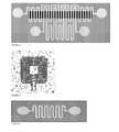
- FIG. 1shows a coreless transformer design
- FIG. 2shows interlocking square spirals etched into APEX® glass.
- FIG. 3Atop view of an inductive device in/on APEX® glass.
- FIG. 3Bside view of an inductive device in/on APEX® glass.
- FIG. 4Ais an image of a free-standing copper RF antenna bridge structure.
- FIG. 4Bis an image of a free-standing coil.
- FIG. 5is an image of a partially etched inductor, where the surrounding ceramic has been partially etched away to allow mostly air to surround the inductive device.
- FIG. 6is an isometric image of a fully etched inductor, where the surrounding ceramic has been fully etched away to allow only air to surround the inductive device.
- FIG. 7A and 7Bare side image of a fully etched inductor, where the surrounding ceramic has been fully etched away to allow only air to surround the inductive device.
- FIG. 1shows a coreless transformer design.
- FIG. 2shows interlocking square spirals etched into APEX® glass.
- FIG. 3Atop view of an inductive device in/on APEX® glass.
- FIG. 3Bside view of an inductive device in/on APEX® glass.
- FIG. 4Ais an image of a free-standing copper RF antenna bridge structure.
- FIG. 4Bis an image of a free-standing coil.
- FIG. 5is an image of a partially etched inductor, where the surrounding ceramic has been partially etched away to allow mostly air to surround the inductive device.
- FIG. 6is an isometric image of a fully etched inductor, where the surrounding ceramic has been fully etched away to allow only air to surround the inductive device.
- FIG. 7A and 7Bare side image of a fully etched inductor, where the surrounding ceramic has been fully etched away to allow only air to surround the inductive device.
- APEX® Glass ceramicis processed using first generation semiconductor equipment in a simple three step process and the final material can be fashioned into either glass, ceramic, or contain regions of both glass and ceramic.
- the APEX® Glass ceramicpossesses several benefits over current materials, including: easily fabricated high density vias, demonstrated microfluidic capability, micro-lens or micro-lens array, high Young's modulus for stiffer packages, halogen free manufacturing, and economical manufacturing.
- Photoetchable glasseshave several advantages for the fabrication of a wide variety of microsystems components.
- Microstructureshave been produced relatively inexpensively with these glasses using conventional semiconductor processing equipment.
- glasseshave high temperature stability, good mechanical and electrically properties, and have better chemical resistance than plastics and many metals.
- FOTURAN®made by Schott Corporation and imported into the U.S. only by Invenios Inc.
- FOTURAN®comprises a lithium-aluminum-silicate glass containing traces of silver ions plus other trace elements specifically silicon oxide (SiO 2 ) of 75-85% by weight, lithium oxide (Li 2 O) of 7-11% by weight, aluminum oxide (Al 2 O 3 ) of 3-6% by weight, sodium oxide (Na 2 O) of 1-2% by weight, 0.2-0.5% by weight antimonium trioxide (Sb2O3) or arsenic oxide (As 2 O 3 ), silver oxide (Ag 2 O) of 0.05-0.15% by weight, and cerium oxide (CeO 2 ) of 0.01-0.04% by weight.
- APEX® Glass ceramic“APEX® glass” or simply “APEX®” is used to denote one embodiment of the glass ceramic composition of the present invention.
- the cerium oxideWhen exposed to UV-light within the absorption band of cerium oxide the cerium oxide acts as sensitizers, absorbing a photon and losing an electron that reduces neighboring silver oxide to form silver atoms, e.g.,
- the silver atomscoalesce into silver nanoclusters during the baking process and induce nucleation sites for crystallization of the surrounding glass. If exposed to UV light through a mask, only the exposed regions of the glass will crystallize during subsequent heat treatment.
- This heat treatmentmust be performed at a temperature near the glass transformation temperature (e.g., greater than 465° C. in air for FOTURAN®).
- the crystalline phaseis more soluble in etchants, such as hydrofluoric acid (HF), than the unexposed vitreous, amorphous regions.
- etchantssuch as hydrofluoric acid (HF)
- HFhydrofluoric acid
- the crystalline regions of FOTURAN®are etched about 20 times faster than the amorphous regions in 10% HF, enabling microstructures with wall slopes ratios of about 20:1 when the exposed regions are removed.
- the shaped glass structurecontains at least one or more, two or three-dimensional inductive device.
- the inductive deviceis formed by making a series of connected loops to form a free-standing inductor.
- the loopscan be either rectangular, circular, elliptical, fractal or other shapes that create and pattern that generates induction.
- the patterned regions of the APEX® glasscan be filled with metal, alloys, composites, glass or other magnetic media, by a number of methods including plating or vapor phase deposition.
- the magnetic permittivity of the media combined with the dimensions and number of structures (loops, turns or other inductive element) in the deviceprovide the inductance of devices. Depending on the frequency of operation the inductive device design will require different magnetic permittivity materials.
- the present inventionprovides a single material approach for the fabrication of optical microstructures with photo-definable/photopatternable APEX® glass for use in imaging applications by the shaped APEX® glass structures that are used for lenses and includes through-layer or in-layer designs.
- glass ceramics materialshave had limited success in microstructure formation plagued by performance, uniformity, usability by others and availability issues.
- Past glass-ceramic materialshave yield etch aspect-ratio of approximately 15:1 in contrast APEX® ⁇ glass has an average etch aspect ratio greater than 50:1. This allows users to create smaller and deeper features. Additionally, our manufacturing process enables product yields of greater than 90% (legacy glass yields are closer to 50%).
- legacy glass ceramicsapproximately only 30% of the glass is converted into the ceramic state, whereas with APEXTM Glass ceramic this conversion is closer to 70%.
- APEX® compositionprovides three main mechanisms for its enhanced performance: (1) The higher amount of silver leads to the formation of smaller ceramic crystals which are etched faster at the grain boundaries, (2) the decrease in silica content (the main constituent etched by the HF acid) decreases the undesired etching of unexposed material, and (3) the higher total weight percent of the alkali metals and boron oxide produces a much more homogeneous glass during manufacturing.
- the present inventionincludes a method for fabricating a glass ceramic structure for use in forming inductive structures used in electromagnetic transmission, transformers and filtering applications.
- the present inventionincludes an inductive structures created in the multiple planes of a glass-ceramic substrate, such process employing the (a) exposure to excitation energy such that the exposure occurs at various angles by either altering the orientation of the substrate or of the energy source, (b) a bake step and (c) an etch step. Angle sizes can be either acute or obtuse.
- the curved and digital structuresare difficult, if not infeasible to create in most glass, ceramic or silicon substrates.
- the present inventionhas created the capability to create such structures in both the vertical as well as horizontal plane for glass-ceramic substrates.
- the present inventionincludes a method for fabricating of an inductive structure on or in a glass ceramic.
- Ceramicization of the glassis accomplished by exposing the entire glass substrate to approximately 20 J/cm 2 of 310 nm light. When trying to create glass spaces within the ceramic, users expose all of the material, except where the glass is to remain glass.
- the present inventionprovides a quartz/chrome mask containing a variety of concentric circles with different diameters.
- the present inventionincludes a method for fabricating an inductive device in or on glass ceramic structure electrical microwave and radio frequency applications.
- the glass ceramic substratemay be a photosensitive glass substrate having a wide number of compositional variations including but not limited to: 60-76 weight % silica; at least 3 weight % K 2 O with 6 weight %-16 weight % of a combination of K 2 O and Na 2 O; 0.003-1 weight % of at least one oxide selected from the group consisting of Ag 2 O and Au 2 O; 0.003-2 weight % Cu 2 O; 0.75 weight %-7 weight % B 2 O 3 , and 6-7 weight % Al 2 O 3 ; with the combination of B 2 O 3 ; and Al 2 O 3 not exceeding 13 weight %; 8-15 weight % Li 2 O; and 0.001-0.1 weight % CeO 2 .
- This and other varied compositionsare generally referred to as the APEX® glass.
- the exposed portionmay be transformed into a crystalline material by heating the glass substrate to a temperature near the glass transformation temperature.
- the anisotropic-etch ratio of the exposed portion to the unexposed portionis at least 30:1 when the glass is exposed to a broad spectrum mid-ultraviolet (about 308-312 nm) flood lamp to provide a shaped glass structure that have an aspect ratio of at least 30:1, and to create an inductive structure.
- the mask for the exposurecan be of a halftone mask that provides a continuous grey scale to the exposure to form a curved structure for the creation of an inductive structure/device.
- a digital maskcan also be used with the flood exposure and can be used to produce the creation of a inductive structure/device.
- the exposed glassis then baked typically in a two-step process. Temperature range heated between of 420° C.-520° C. for between 10 minutes to 2 hours, for the coalescing of silver ions into silver nanoparticles and temperature range heated between 520° C.-620° C. for between 10 minutes and 2 hours allowing the lithium oxide to form around the silver nanoparticles.
- the glass plateis then etched.
- the glass substrateis etched in an etchant, of HF solution, typically 5% to 10% by volume, wherein the etch ratio of exposed portion to that of the unexposed portion is at least 30:1 when exposed with a broad spectrum mid-ultraviolet flood light, and greater than 30:1 when exposed with a laser, to provide a shaped glass structure with an anisotropic-etch ratio of at least 30:1.
- an etchantof HF solution, typically 5% to 10% by volume, wherein the etch ratio of exposed portion to that of the unexposed portion is at least 30:1 when exposed with a broad spectrum mid-ultraviolet flood light, and greater than 30:1 when exposed with a laser, to provide a shaped glass structure with an anisotropic-etch ratio of at least 30:1.
- the material surrounding the inductive deviceis converted to ceramic before metal filling.
- the metallic material used to fill the etched structuresis metal other than copper (i.e. nickel, iron alloys).
- the surface of the inductive deviceis coated with a dielectric material.
- the surface of the inductive deviceis patterned first with a dielectric material and then with a patterned metal.
- an inductive deviceconsisting of multiple unique inductive components. Said device where different inductive components are selectively plated with different metals into different etched features.
Landscapes
- Engineering & Computer Science (AREA)
- Power Engineering (AREA)
- Chemical & Material Sciences (AREA)
- Manufacturing & Machinery (AREA)
- Microelectronics & Electronic Packaging (AREA)
- Life Sciences & Earth Sciences (AREA)
- Chemical Kinetics & Catalysis (AREA)
- General Chemical & Material Sciences (AREA)
- Geochemistry & Mineralogy (AREA)
- Materials Engineering (AREA)
- Organic Chemistry (AREA)
- Physics & Mathematics (AREA)
- General Physics & Mathematics (AREA)
- Condensed Matter Physics & Semiconductors (AREA)
- Ceramic Engineering (AREA)
- Computer Hardware Design (AREA)
- Dispersion Chemistry (AREA)
- Crystallography & Structural Chemistry (AREA)
- Thermal Sciences (AREA)
- Inorganic Chemistry (AREA)
- Glass Compositions (AREA)
- Manufacturing Cores, Coils, And Magnets (AREA)
- Coils Or Transformers For Communication (AREA)
Abstract
Description
- The present invention relates to creating an inductive current device in a photo definable glass structure, in particular, creating Inductors, Antenna, and Transformers devices and arrays in glass ceramic substrates for electronic, microwave and radiofrequency in general.
- Photosensitive glass structures have been suggested for a number of micromachining and microfabrication processes such as integrated electronic elements in conjunction with other elements systems or subsystems. Silicon microfabrication of traditional glass is expensive and low yield while injection modeling or embossing processes produce inconsistent shapes. Silicon microfabrication processes rely on expensive capital equipment; photolithography and reactive ion etching or ion beam milling tools that generally cost in excess of one million dollars each and require an ultra-clean, high-production silicon fabrication facility costing millions to billions more. Injection molding and embossing are less costly methods of producing a three dimensional shapes but generate defects with in the transfer or have differences due to the stochastic curing process.
- The present invention provides creates a cost effective glass ceramic inductive individual or array device. Where glass ceramic substrate has demonstrated capability to form such structures through the processing of both the vertical as well as horizontal planes either separately or at the same time to form, two or three-dimensional inductive devices.
- The present invention includes a method to fabricate a substrate with one or more, two or three dimensional inductive device by preparing a photosensitive glass substrate and further coating or filling with one or more metals.
- A method of fabrication and device made by preparing a photosensitive glass ceramic composite substrate comprising at least silica, lithium oxide, aluminum oxide, and cerium oxide, masking a design layout comprising one or more, two or three dimensional inductive device in the photosensitive glass substrate, exposing at least one portion of the photosensitive glass substrate to an activating energy source, exposing the photosensitive glass substrate to a heating phase of at least ten minutes above its glass transition temperature, cooling the photosensitive glass substrate to transform at least part of the exposed glass to a crystalline material to form a glass-crystalline substrate and etching the glass-crystalline substrate with an etchant solution to form one or more angled channels or through holes that are then used in the inductive device.
- The present invention provides a method to fabricate an inductive device created in or on photo-definable glass comprising the steps of: preparing a photosensitive glass substrate comprising at least silica, lithium oxide, aluminum oxide, and cerium oxide; masking a design layout comprising one or more structures to form one or more electrical conduction paths on the photosensitive glass substrate; exposing at least one portion of the photosensitive glass substrate to an activating energy source; exposing the photosensitive glass substrate to a heating phase of at least ten minutes above its glass transition temperature; cooling the photosensitive glass substrate to transform at least part of the exposed glass to a crystalline material to form a glass-crystalline substrate; etching the glass-crystalline substrate with an etchant solution to form the one or more angled channels in the device; wherein the glass-crystalline substrate adjacent to the trenches may also be converted to a ceramic phase; coating the one or more angled channels with one or more metals; coating all or part of the inductor structure with a dielectric media; removing all or part of the dielectric media to provide electrical contact or free standing inductive device; and wherein the metal is connected to a circuitry through a surface or buried contact.
- The inductive device stores current and functions as a current storage device. The one or more metals are designed to operate as an inductor at the appropriate frequencies. The inductive device has a magnetic permeability greater than or equal to copper for frequencies greater than 100 MHz. The inductive device has a magnetic permeability greater than copper for frequencies less than 100 MHz. The ceramic phase can be etched from one side or both sides to partially or fully remove the glass-ceramic material. The method can further include the step of converting at least a portion of the glass into ceramic and etching away the ceramic to at least partially expose the metal structure. The method can further include the step of converting at least a portion of the glass into ceramic and etching away the ceramic to fully expose the metal structure.
- The present invention also includes an inductive device having a glass-ceramic material surrounding one or more inductive coils wherein the one or more inductive coils are at least partially surround by air.
- The one or more inductive coils include one or more angled channels in the glass-crystalline substrate with a metal coating over at least a portion of the one or more angled channels. The inductive element is further surrounded by a magnetically permeable material. The inductive element does not touch the magnetically permeable material. The inductive element comprises a cavity filled with a magnetically permeable material on one side, both sides or through the glass-ceramic material. The one or more inductors interact with each other. The one or more inductors share a magnetically permeable material. The metal coating may reside partially through, fully through, or on top of the glass-ceramic material, or a combination there of The inductive device of further includes 1 or more second metal layer on any surface.
- The present invention also includes an inductive device having a glass-crystalline substrate surrounding one or more inductive coils wherein the one or more inductive coils are at least partially surround by air. The inductive device includes one or more inductive coils are that are supported by one or more rails on the glass-crystalline substrate. The inductive device includes one or more inductive coils are that are positioned in one or more pits in the glass-crystalline substrate. The inductive device may include a metal coating, a multilayer metal coating, an alloy coating, a multilayer alloy coating.
- For a more complete understanding of the features and advantages of the present invention, reference is now made to the detailed description of the invention along with the accompanying figures and in which:
FIG. 1 shows a coreless transformer design.FIG. 2 shows interlocking square spirals etched into APEX® glass.FIG. 3A top view of an inductive device in/on APEX® glass.FIG. 3B side view of an inductive device in/on APEX® glass.FIG. 4A is an image of a free-standing copper RF antenna bridge structure.FIG. 4B is an image of a free-standing coil.FIG. 5 is an image of a partially etched inductor, where the surrounding ceramic has been partially etched away to allow mostly air to surround the inductive device.FIG. 6 is an isometric image of a fully etched inductor, where the surrounding ceramic has been fully etched away to allow only air to surround the inductive device.FIG. 7A and 7B are side image of a fully etched inductor, where the surrounding ceramic has been fully etched away to allow only air to surround the inductive device.- While the making and using of various embodiments of the present invention are discussed in detail below, it should be appreciated that the present invention provides many applicable inventive concepts that can be embodied in a wide variety of specific contexts. The specific embodiments discussed herein are merely illustrative of specific ways to make and use the invention and do not restrict the scope of the invention.
- To facilitate the understanding of this invention, a number of terms are defined below. Terms defined herein have meanings as commonly understood by a person of ordinary skill in the areas relevant to the present invention. Terms such as “a”, “an” and “the” are not intended to refer to only a singular entity, but include the general class of which a specific example may be used for illustration. The terminology herein is used to describe specific embodiments of the invention, but their usage does not delimit the invention, except as outlined in the claims.
FIG. 1 shows a coreless transformer design.FIG. 2 shows interlocking square spirals etched into APEX® glass.FIG. 3A top view of an inductive device in/on APEX® glass.FIG. 3B side view of an inductive device in/on APEX® glass.FIG. 4A is an image of a free-standing copper RF antenna bridge structure.FIG. 4B is an image of a free-standing coil.FIG. 5 is an image of a partially etched inductor, where the surrounding ceramic has been partially etched away to allow mostly air to surround the inductive device.FIG. 6 is an isometric image of a fully etched inductor, where the surrounding ceramic has been fully etched away to allow only air to surround the inductive device.FIG. 7A and 7B are side image of a fully etched inductor, where the surrounding ceramic has been fully etched away to allow only air to surround the inductive device.- To address these needs, the present inventors developed a glass ceramic (APEX®) Glass ceramic) as a novel packaging and substrate material for semiconductors, RF electronics, microwave electronics, and optical imaging. APEX® Glass ceramic is processed using first generation semiconductor equipment in a simple three step process and the final material can be fashioned into either glass, ceramic, or contain regions of both glass and ceramic. The APEX® Glass ceramic possesses several benefits over current materials, including: easily fabricated high density vias, demonstrated microfluidic capability, micro-lens or micro-lens array, high Young's modulus for stiffer packages, halogen free manufacturing, and economical manufacturing. Photoetchable glasses have several advantages for the fabrication of a wide variety of microsystems components. Microstructures have been produced relatively inexpensively with these glasses using conventional semiconductor processing equipment. In general, glasses have high temperature stability, good mechanical and electrically properties, and have better chemical resistance than plastics and many metals. To our knowledge, the only commercially available photoetchable glass is FOTURAN®, made by Schott Corporation and imported into the U.S. only by Invenios Inc. FOTURAN® comprises a lithium-aluminum-silicate glass containing traces of silver ions plus other trace elements specifically silicon oxide (SiO2) of 75-85% by weight, lithium oxide (Li2O) of 7-11% by weight, aluminum oxide (Al2O3) of 3-6% by weight, sodium oxide (Na2O) of 1-2% by weight, 0.2-0.5% by weight antimonium trioxide (Sb2O3) or arsenic oxide (As2O3), silver oxide (Ag2O) of 0.05-0.15% by weight, and cerium oxide (CeO2) of 0.01-0.04% by weight. As used herein the terms “APEX® Glass ceramic”, “APEX® glass” or simply “APEX®” is used to denote one embodiment of the glass ceramic composition of the present invention.
- When exposed to UV-light within the absorption band of cerium oxide the cerium oxide acts as sensitizers, absorbing a photon and losing an electron that reduces neighboring silver oxide to form silver atoms, e.g.,
Ce3++Ag+=Ce4++Ag0- The silver atoms coalesce into silver nanoclusters during the baking process and induce nucleation sites for crystallization of the surrounding glass. If exposed to UV light through a mask, only the exposed regions of the glass will crystallize during subsequent heat treatment.
- This heat treatment must be performed at a temperature near the glass transformation temperature (e.g., greater than 465° C. in air for FOTURAN®). The crystalline phase is more soluble in etchants, such as hydrofluoric acid (HF), than the unexposed vitreous, amorphous regions. In particular, the crystalline regions of FOTURAN® are etched about 20 times faster than the amorphous regions in 10% HF, enabling microstructures with wall slopes ratios of about 20:1 when the exposed regions are removed. See T. R. Dietrich et al., “Fabrication technologies for microsystems utilizing photoetchable glass,” Microelectronic Engineering 30, 497 (1996), which is incorporated herein by reference. Preferably, the shaped glass structure contains at least one or more, two or three-dimensional inductive device. The inductive device is formed by making a series of connected loops to form a free-standing inductor. The loops can be either rectangular, circular, elliptical, fractal or other shapes that create and pattern that generates induction. The patterned regions of the APEX® glass can be filled with metal, alloys, composites, glass or other magnetic media, by a number of methods including plating or vapor phase deposition. The magnetic permittivity of the media combined with the dimensions and number of structures (loops, turns or other inductive element) in the device provide the inductance of devices. Depending on the frequency of operation the inductive device design will require different magnetic permittivity materials. At low frequencies, less than 100 MHz devices can use ferrites or other high different magnetic permittivity materials. At higher frequencies >100 MHz high different magnetic permittivity materials can generate eddy currents creating large electrical losses. So at higher frequency operations material such as copper or other similar material is the media of choice for inductive devices. Once the inductive device has been generated the supporting APEX® glass can be left in place or removed to create a free-standing structure. The present invention provides a single material approach for the fabrication of optical microstructures with photo-definable/photopatternable APEX® glass for use in imaging applications by the shaped APEX® glass structures that are used for lenses and includes through-layer or in-layer designs.
- Generally, glass ceramics materials have had limited success in microstructure formation plagued by performance, uniformity, usability by others and availability issues. Past glass-ceramic materials have yield etch aspect-ratio of approximately 15:1 in contrast APEX®β glass has an average etch aspect ratio greater than 50:1. This allows users to create smaller and deeper features. Additionally, our manufacturing process enables product yields of greater than 90% (legacy glass yields are closer to 50%). Lastly, in legacy glass ceramics, approximately only 30% of the glass is converted into the ceramic state, whereas with APEX™ Glass ceramic this conversion is closer to 70%.
- APEX® composition provides three main mechanisms for its enhanced performance: (1) The higher amount of silver leads to the formation of smaller ceramic crystals which are etched faster at the grain boundaries, (2) the decrease in silica content (the main constituent etched by the HF acid) decreases the undesired etching of unexposed material, and (3) the higher total weight percent of the alkali metals and boron oxide produces a much more homogeneous glass during manufacturing.
- The present invention includes a method for fabricating a glass ceramic structure for use in forming inductive structures used in electromagnetic transmission, transformers and filtering applications. The present invention includes an inductive structures created in the multiple planes of a glass-ceramic substrate, such process employing the (a) exposure to excitation energy such that the exposure occurs at various angles by either altering the orientation of the substrate or of the energy source, (b) a bake step and (c) an etch step. Angle sizes can be either acute or obtuse. The curved and digital structures are difficult, if not infeasible to create in most glass, ceramic or silicon substrates. The present invention has created the capability to create such structures in both the vertical as well as horizontal plane for glass-ceramic substrates. The present invention includes a method for fabricating of an inductive structure on or in a glass ceramic.
- Ceramicization of the glass is accomplished by exposing the entire glass substrate to approximately 20 J/cm2of 310 nm light. When trying to create glass spaces within the ceramic, users expose all of the material, except where the glass is to remain glass. In one embodiment, the present invention provides a quartz/chrome mask containing a variety of concentric circles with different diameters.
- The present invention includes a method for fabricating an inductive device in or on glass ceramic structure electrical microwave and radio frequency applications. The glass ceramic substrate may be a photosensitive glass substrate having a wide number of compositional variations including but not limited to: 60-76 weight % silica; at least 3 weight % K2O with 6 weight %-16 weight % of a combination of K2O and Na2O; 0.003-1 weight % of at least one oxide selected from the group consisting of Ag2O and Au2O; 0.003-2 weight % Cu2O; 0.75 weight %-7 weight % B2O3, and 6-7 weight % Al2O3; with the combination of B2O3; and Al2O3not exceeding 13 weight %; 8-15 weight % Li2O; and 0.001-0.1 weight % CeO2. This and other varied compositions are generally referred to as the APEX® glass.
- The exposed portion may be transformed into a crystalline material by heating the glass substrate to a temperature near the glass transformation temperature. When etching the glass substrate in an etchant such as hydrofluoric acid, the anisotropic-etch ratio of the exposed portion to the unexposed portion is at least 30:1 when the glass is exposed to a broad spectrum mid-ultraviolet (about 308-312 nm) flood lamp to provide a shaped glass structure that have an aspect ratio of at least 30:1, and to create an inductive structure. The mask for the exposure can be of a halftone mask that provides a continuous grey scale to the exposure to form a curved structure for the creation of an inductive structure/device. A digital mask can also be used with the flood exposure and can be used to produce the creation of a inductive structure/device. The exposed glass is then baked typically in a two-step process. Temperature range heated between of 420° C.-520° C. for between 10 minutes to 2 hours, for the coalescing of silver ions into silver nanoparticles and temperature range heated between 520° C.-620° C. for between 10 minutes and 2 hours allowing the lithium oxide to form around the silver nanoparticles. The glass plate is then etched. The glass substrate is etched in an etchant, of HF solution, typically 5% to 10% by volume, wherein the etch ratio of exposed portion to that of the unexposed portion is at least 30:1 when exposed with a broad spectrum mid-ultraviolet flood light, and greater than 30:1 when exposed with a laser, to provide a shaped glass structure with an anisotropic-etch ratio of at least 30:1.
- Where the material surrounding the inductive device is converted to ceramic before metal filling. Where the metallic material used to fill the etched structures is metal other than copper (i.e. nickel, iron alloys). Where the surface of the inductive device is coated with a dielectric material. Where the surface of the inductive device is patterned first with a dielectric material and then with a patterned metal.
- For embodiments that are surrounded by the ceramic phase: Where the ceramic is etched from one side or both sides to partially or fully remove the glass-ceramic material to partially expose the metal structures. An inductive device consisting of multiple unique inductive components. Said device where different inductive components are selectively plated with different metals into different etched features.
Claims (18)
Priority Applications (1)
| Application Number | Priority Date | Filing Date | Title |
|---|---|---|---|
| US15/308,583US10665377B2 (en) | 2014-05-05 | 2015-05-05 | 2D and 3D inductors antenna and transformers fabricating photoactive substrates |
Applications Claiming Priority (3)
| Application Number | Priority Date | Filing Date | Title |
|---|---|---|---|
| US201461988615P | 2014-05-05 | 2014-05-05 | |
| US15/308,583US10665377B2 (en) | 2014-05-05 | 2015-05-05 | 2D and 3D inductors antenna and transformers fabricating photoactive substrates |
| PCT/US2015/029222WO2015171597A1 (en) | 2014-05-05 | 2015-05-05 | 2d and 3d inductors antenna and transformers fabricating photoactive substrates |
Related Parent Applications (1)
| Application Number | Title | Priority Date | Filing Date |
|---|---|---|---|
| PCT/US2015/029222A-371-Of-InternationalWO2015171597A1 (en) | 2014-05-05 | 2015-05-05 | 2d and 3d inductors antenna and transformers fabricating photoactive substrates |
Related Child Applications (1)
| Application Number | Title | Priority Date | Filing Date |
|---|---|---|---|
| US16/850,571ContinuationUS11929199B2 (en) | 2014-05-05 | 2020-04-16 | 2D and 3D inductors fabricating photoactive substrates |
Publications (2)
| Publication Number | Publication Date |
|---|---|
| US20170098501A1true US20170098501A1 (en) | 2017-04-06 |
| US10665377B2 US10665377B2 (en) | 2020-05-26 |
Family
ID=54392897
Family Applications (2)
| Application Number | Title | Priority Date | Filing Date |
|---|---|---|---|
| US15/308,583Active2035-06-28US10665377B2 (en) | 2014-05-05 | 2015-05-05 | 2D and 3D inductors antenna and transformers fabricating photoactive substrates |
| US16/850,571Active2036-10-23US11929199B2 (en) | 2014-05-05 | 2020-04-16 | 2D and 3D inductors fabricating photoactive substrates |
Family Applications After (1)
| Application Number | Title | Priority Date | Filing Date |
|---|---|---|---|
| US16/850,571Active2036-10-23US11929199B2 (en) | 2014-05-05 | 2020-04-16 | 2D and 3D inductors fabricating photoactive substrates |
Country Status (5)
| Country | Link |
|---|---|
| US (2) | US10665377B2 (en) |
| EP (2) | EP3140838B1 (en) |
| JP (1) | JP6574207B2 (en) |
| KR (1) | KR101940981B1 (en) |
| WO (1) | WO2015171597A1 (en) |
Cited By (18)
| Publication number | Priority date | Publication date | Assignee | Title |
|---|---|---|---|---|
| US10070533B2 (en) | 2015-09-30 | 2018-09-04 | 3D Glass Solutions, Inc. | Photo-definable glass with integrated electronics and ground plane |
| WO2018200804A1 (en)* | 2017-04-28 | 2018-11-01 | 3D Glass Solutions, Inc. | Rf circulator |
| WO2019118761A1 (en)* | 2017-12-15 | 2019-06-20 | 3D Glass Solutions, Inc. | Coupled transmission line resonate rf filter |
| WO2019231947A1 (en)* | 2018-05-29 | 2019-12-05 | 3D Glass Solutions, Inc. | Low insertion loss rf transmission line |
| EP3649733A4 (en)* | 2017-07-07 | 2020-05-13 | 3D Glass Solutions, Inc. | 2D AND 3D RF EMBOSSED ELEMENT DEVICES FOR RF SYSTEM IN GROUP PHOTOACTIVE GLASS SUBSTRATES |
| US11076489B2 (en) | 2018-04-10 | 2021-07-27 | 3D Glass Solutions, Inc. | RF integrated power condition capacitor |
| US11139582B2 (en) | 2018-09-17 | 2021-10-05 | 3D Glass Solutions, Inc. | High efficiency compact slotted antenna with a ground plane |
| US11161773B2 (en) | 2016-04-08 | 2021-11-02 | 3D Glass Solutions, Inc. | Methods of fabricating photosensitive substrates suitable for optical coupler |
| KR20210142753A (en)* | 2019-04-18 | 2021-11-25 | 3디 글래스 솔루션즈 인코포레이티드 | High-efficiency die dicing and release |
| US11264167B2 (en) | 2016-02-25 | 2022-03-01 | 3D Glass Solutions, Inc. | 3D capacitor and capacitor array fabricating photoactive substrates |
| US20220068554A1 (en)* | 2020-09-03 | 2022-03-03 | Murata Manufacturing Co., Ltd. | Electronic component and electronic component module |
| US11270843B2 (en) | 2018-12-28 | 2022-03-08 | 3D Glass Solutions, Inc. | Annular capacitor RF, microwave and MM wave systems |
| US20220377904A1 (en)* | 2019-10-14 | 2022-11-24 | 3D Glass Solutions, Inc. | High temperature printed circuit board substrate |
| US11594457B2 (en) | 2018-12-28 | 2023-02-28 | 3D Glass Solutions, Inc. | Heterogenous integration for RF, microwave and MM wave systems in photoactive glass substrates |
| WO2023091295A1 (en)* | 2021-11-18 | 2023-05-25 | Corning Incorporated | Methods for producing localized crystallization in glass articles and glass articles formed therefrom |
| US11677373B2 (en) | 2018-01-04 | 2023-06-13 | 3D Glass Solutions, Inc. | Impedence matching conductive structure for high efficiency RF circuits |
| US11929199B2 (en) | 2014-05-05 | 2024-03-12 | 3D Glass Solutions, Inc. | 2D and 3D inductors fabricating photoactive substrates |
| US12009143B2 (en)* | 2018-08-08 | 2024-06-11 | Endress+Hauser Flowtec Ag | Method of producing a coil device, coil device, measuring transducer with coil device, instrument having a measuring transducer |
Families Citing this family (5)
| Publication number | Priority date | Publication date | Assignee | Title |
|---|---|---|---|---|
| KR101887106B1 (en)* | 2016-10-31 | 2018-08-09 | 아비코전자 주식회사 | Micro Inductor and Method of Manufacturing the Same |
| WO2020014661A1 (en) | 2018-07-13 | 2020-01-16 | Knowles Cazenovia, Inc. | Millimeter wave filter array |
| JP7140435B2 (en) | 2019-04-05 | 2022-09-21 | スリーディー グラス ソリューションズ,インク | Glass-based empty substrate integrated waveguide device |
| KR20220164800A (en)* | 2020-04-17 | 2022-12-13 | 3디 글래스 솔루션즈 인코포레이티드 | broadband inductor |
| US20240014794A1 (en)* | 2020-05-26 | 2024-01-11 | 3D Glass Solutions, Inc. | Impedence Matching Conductive Structure for High Efficiency RF Circuits |
Citations (14)
| Publication number | Priority date | Publication date | Assignee | Title |
|---|---|---|---|---|
| US3904991A (en)* | 1973-02-12 | 1975-09-09 | Tokyo Shibaura Electric Co | Stripline directional coupler having bent coupling arms |
| US5371466A (en)* | 1992-07-29 | 1994-12-06 | The Regents Of The University Of California | MRI RF ground breaker assembly |
| US6373369B2 (en)* | 1999-07-26 | 2002-04-16 | Taiwan Semiconductor Manufacturing Company | High efficiency thin film inductor |
| US6686824B1 (en)* | 1998-05-29 | 2004-02-03 | Nissha Printing Co., Ltd. | Toroidal printed coil |
| US20040155748A1 (en)* | 2003-02-02 | 2004-08-12 | Dietrich Steingroever | Transformer for producing high electrical currents |
| US20060283948A1 (en)* | 2005-06-20 | 2006-12-21 | Denso Corporation | Antenna coil, resonant antenna having antenna coil, and card type wireless device having resonant antenna |
| US20070296520A1 (en)* | 2005-04-18 | 2007-12-27 | Murata Manufacturing Co., Ltd. | High-frequency module |
| US20090243783A1 (en)* | 2006-08-28 | 2009-10-01 | Avago Technologies Ecbu (Singapore) Pte. Ltd. | Minimizing Electromagnetic Interference in Coil Transducers |
| US20100058583A1 (en)* | 2005-06-21 | 2010-03-11 | Florent Cros | Method of manufacturing implantable wireless sensor for in vivo pressure measurement |
| US20100237462A1 (en)* | 2009-03-18 | 2010-09-23 | Benjamin Beker | Package Level Tuning Techniques for Propagation Channels of High-Speed Signals |
| US7948342B2 (en)* | 2008-07-24 | 2011-05-24 | Cutt-A-Watt Enterprises, Llc | Electromotive rectification system |
| US20140203891A1 (en)* | 2012-01-16 | 2014-07-24 | Murata Manufacturing Co., Ltd. | Rf signal blocking device |
| US20150048901A1 (en)* | 2013-08-19 | 2015-02-19 | Harris Corporation | Microelectromechanical systems comprising differential inductors and methods for making the same |
| US9449753B2 (en)* | 2013-08-30 | 2016-09-20 | Qualcomm Incorporated | Varying thickness inductor |
Family Cites Families (300)
| Publication number | Priority date | Publication date | Assignee | Title |
|---|---|---|---|---|
| NL69675C (en) | 1943-12-08 | |||
| GB619779A (en) | 1946-01-18 | 1949-03-15 | Gen Aniline & Film Corp | Improvements in iron powder and cores produced therefrom |
| FR958680A (en) | 1946-09-09 | 1950-03-17 | ||
| US2515941A (en) | 1946-09-09 | 1950-07-18 | Corning Glass Works | Photosensitive opal glass |
| BE493137A (en) | 1949-01-07 | |||
| BE513836A (en) | 1951-08-30 | |||
| US2628160A (en) | 1951-08-30 | 1953-02-10 | Corning Glass Works | Sculpturing glass |
| US2971853A (en) | 1953-03-05 | 1961-02-14 | Corning Glass Works | Ceramic body and method of making it |
| US3281264A (en) | 1963-01-31 | 1966-10-25 | Coast Metals Inc | Method of gold-plating aluminum |
| US3292115A (en) | 1964-09-11 | 1966-12-13 | Hazeltine Research Inc | Easily fabricated waveguide structures |
| GB1407151A (en) | 1973-02-13 | 1975-09-24 | Okikiolu G O | System assemblies of energized components having tapering form for developing progressively increasing electromagnetic energy fields |
| US3993401A (en) | 1975-02-10 | 1976-11-23 | Minnesota Mining And Manufacturing Company | Retroreflective material including geometric fresnel zone plates |
| US3985531A (en) | 1975-03-19 | 1976-10-12 | Corning Glass Works | Spontaneously-formed fluormica glass-ceramics |
| US4029605A (en) | 1975-12-08 | 1977-06-14 | Hercules Incorporated | Metallizing compositions |
| US4413061A (en) | 1978-02-06 | 1983-11-01 | International Business Machines Corporation | Glass-ceramic structures and sintered multilayer substrates thereof with circuit patterns of gold, silver or copper |
| JPS56155587A (en) | 1980-05-02 | 1981-12-01 | Fujitsu Ltd | Printed circuit board |
| JPS57200042A (en) | 1981-06-02 | 1982-12-08 | Hoya Corp | Exposure method for chemically machinable photosensitive glass |
| US4537612A (en) | 1982-04-01 | 1985-08-27 | Corning Glass Works | Colored photochromic glasses and method |
| JPS5939949U (en)* | 1982-09-08 | 1984-03-14 | アルプス電気株式会社 | High frequency circuit equipment |
| US4647940A (en) | 1982-09-27 | 1987-03-03 | Rogers Corporation | Parallel plate waveguide antenna |
| US5078771A (en) | 1989-02-07 | 1992-01-07 | Canyon Materials, Inc. | Method of making high energy beam sensitive glasses |
| US4514053A (en) | 1983-08-04 | 1985-04-30 | Corning Glass Works | Integral photosensitive optical device and method |
| JPS61149905A (en) | 1984-12-25 | 1986-07-08 | Fujitsu Ltd | Optical multiplexer and demultiplexer |
| JPS61231529A (en) | 1985-04-08 | 1986-10-15 | Agency Of Ind Science & Technol | Optical control type optical switch device |
| JPS62202840A (en) | 1986-03-03 | 1987-09-07 | Toshiba Corp | Working of photosensitive glass |
| US4692015A (en) | 1986-03-14 | 1987-09-08 | Xerox Corporation | Short focal lens array with multi-magnification properties |
| JPS63128699A (en) | 1986-11-19 | 1988-06-01 | 株式会社日立製作所 | Light-sensitive glass-ceramic multilayer interconnection board |
| US4788165A (en) | 1987-10-07 | 1988-11-29 | Corning Glass Works | Copper-exuding, boroaluminosilicate glasses |
| CA1320507C (en) | 1987-10-07 | 1993-07-20 | Elizabeth A. Boylan | Thermal writing on glass or glass-ceramic substrates and copper-exuding glasses |
| US4942076A (en) | 1988-11-03 | 1990-07-17 | Micro Substrates, Inc. | Ceramic substrate with metal filled via holes for hybrid microcircuits and method of making the same |
| JP2737292B2 (en) | 1989-09-01 | 1998-04-08 | 富士通株式会社 | Copper paste and metallizing method using the same |
| US5147740A (en) | 1990-08-09 | 1992-09-15 | Rockwell International Corporation | Structure and process for fabricating conductive patterns having sub-half micron dimensions |
| US5215610A (en) | 1991-04-04 | 1993-06-01 | International Business Machines Corporation | Method for fabricating superconductor packages |
| BE1004844A7 (en) | 1991-04-12 | 1993-02-09 | Laude Lucien Diego | Metallisation methods surface using metal powder. |
| US5212120A (en) | 1991-06-10 | 1993-05-18 | Corning Incorporated | Photosensitive glass |
| US5395498A (en) | 1991-11-06 | 1995-03-07 | Gombinsky; Moshe | Method for separating biological macromolecules and means therfor |
| JPH05139787A (en) | 1991-11-19 | 1993-06-08 | Seikosha Co Ltd | Working method for photosensitive glass |
| US5374291A (en) | 1991-12-10 | 1994-12-20 | Director-General Of Agency Of Industrial Science And Technology | Method of processing photosensitive glass |
| JPH05206706A (en) | 1992-01-30 | 1993-08-13 | Reader Denshi Kk | Interdigital type band pass filter |
| US6258497B1 (en) | 1992-07-29 | 2001-07-10 | International Business Machines Corporation | Precise endpoint detection for etching processes |
| US5312674A (en)* | 1992-07-31 | 1994-05-17 | Hughes Aircraft Company | Low-temperature-cofired-ceramic (LTCC) tape structures including cofired ferromagnetic elements, drop-in components and multi-layer transformer |
| US6017681A (en) | 1992-11-09 | 2000-01-25 | Fujitsu Limited | Method of coupling optical parts and method of forming a mirror |
| GB2290171B (en) | 1994-06-03 | 1998-01-21 | Plessey Semiconductors Ltd | Inductor chip device |
| JPH0826767A (en) | 1994-07-13 | 1996-01-30 | Nippon Glass Kk | Soda lime-silica photosensitive glass and its production |
| JPH08179155A (en) | 1994-12-26 | 1996-07-12 | Ricoh Co Ltd | Method for coupling lens and optical fiber and method for producing lens substrate |
| JP3438383B2 (en) | 1995-03-03 | 2003-08-18 | ソニー株式会社 | Polishing method and polishing apparatus used therefor |
| CA2704228C (en) | 1995-03-10 | 2013-10-22 | Meso Scale Technologies, Llc | Multi-array, multi-specific electrochemiluminescence testing |
| US5919607A (en) | 1995-10-26 | 1999-07-06 | Brown University Research Foundation | Photo-encoded selective etching for glass based microtechnology applications |
| US5733370A (en)* | 1996-01-16 | 1998-03-31 | Seagate Technology, Inc. | Method of manufacturing a bicrystal cluster magnetic recording medium |
| JPH107435A (en)* | 1996-06-26 | 1998-01-13 | Ngk Spark Plug Co Ltd | Glass ceramic wiring substrate and its production |
| DE69739727D1 (en) | 1996-09-26 | 2010-02-11 | Asahi Glass Co Ltd | Protective plate for a plasma display and method of making the same |
| US6562523B1 (en) | 1996-10-31 | 2003-05-13 | Canyon Materials, Inc. | Direct write all-glass photomask blanks |
| JPH10199728A (en) | 1997-01-07 | 1998-07-31 | Murata Mfg Co Ltd | Thin-film coil component and method of manufacturing the same |
| US5850623A (en) | 1997-03-14 | 1998-12-15 | Eastman Chemical Company | Method for standardizing raman spectrometers to obtain stable and transferable calibrations |
| JP2000512810A (en) | 1997-04-25 | 2000-09-26 | コーニンクレッカ フィリップス エレクトロニクス エヌ ヴィ | Method of manufacturing encapsulated multilayer capacitor and encapsulated multilayer capacitor |
| US5998224A (en) | 1997-05-16 | 1999-12-07 | Abbott Laboratories | Magnetically assisted binding assays utilizing a magnetically responsive reagent |
| US6287965B1 (en) | 1997-07-28 | 2001-09-11 | Samsung Electronics Co, Ltd. | Method of forming metal layer using atomic layer deposition and semiconductor device having the metal layer as barrier metal layer or upper or lower electrode of capacitor |
| US6417754B1 (en) | 1997-12-08 | 2002-07-09 | The Regents Of The University Of California | Three-dimensional coil inductor |
| JPH11176815A (en) | 1997-12-15 | 1999-07-02 | Ricoh Co Ltd | Dry etching end point determination method and dry etching apparatus |
| US6598291B2 (en) | 1998-03-20 | 2003-07-29 | Viasystems, Inc. | Via connector and method of making same |
| US6115521A (en) | 1998-05-07 | 2000-09-05 | Trw Inc. | Fiber/waveguide-mirror-lens alignment device |
| US6171886B1 (en) | 1998-06-30 | 2001-01-09 | Eastman Kodak Company | Method of making integrated hybrid silicon-based micro-actuator devices |
| US6046641A (en) | 1998-07-22 | 2000-04-04 | Eni Technologies, Inc. | Parallel HV MOSFET high power stable amplifier |
| JP2000114818A (en) | 1998-10-07 | 2000-04-21 | Hitachi Metals Ltd | Concentrated constant nonreversible circuit element |
| JP2000199827A (en) | 1998-10-27 | 2000-07-18 | Sony Corp | Optical wave guide device and its manufacture |
| US6136210A (en) | 1998-11-02 | 2000-10-24 | Xerox Corporation | Photoetching of acoustic lenses for acoustic ink printing |
| JP2000228615A (en)* | 1999-02-05 | 2000-08-15 | Tokin Corp | Lc bandpass filter |
| US6511793B1 (en) | 1999-03-24 | 2003-01-28 | Lg Electronics Inc. | Method of manufacturing microstructure using photosensitive glass substrate |
| US6485690B1 (en) | 1999-05-27 | 2002-11-26 | Orchid Biosciences, Inc. | Multiple fluid sample processor and system |
| JP3756041B2 (en) | 1999-05-27 | 2006-03-15 | Hoya株式会社 | Manufacturing method of multilayer printed wiring board |
| FR2795745B1 (en) | 1999-06-30 | 2001-08-03 | Saint Gobain Vitrage | PROCESS FOR DEPOSITING A TUNGSTENE AND / OR MOLYBDENE LAYER ON A GLASS, CERAMIC OR VITROCERAMIC SUBSTRATE, AND SUBSTRATE THUS COATED |
| JP2001033664A (en) | 1999-07-21 | 2001-02-09 | Hitachi Cable Ltd | Optical fiber block |
| US7179638B2 (en) | 1999-07-30 | 2007-02-20 | Large Scale Biology Corporation | Microarrays and their manufacture by slicing |
| US6538775B1 (en) | 1999-09-16 | 2003-03-25 | Reveo, Inc. | Holographically-formed polymer dispersed liquid crystals with multiple gratings |
| US6403286B1 (en) | 1999-11-04 | 2002-06-11 | Corning Incorporated | High aspect ratio patterning of glass film |
| JP2001206735A (en) | 2000-01-25 | 2001-07-31 | Central Glass Co Ltd | Plating method |
| JP4200631B2 (en) | 2000-03-29 | 2008-12-24 | 沖電気工業株式会社 | On-chip coil and its manufacturing method |
| US6579817B2 (en) | 2000-04-26 | 2003-06-17 | Matsushita Electric Industrial Co., Ltd. | Dielectric ceramic composition and method for producing the same, and device for communication apparatus using the same |
| US6329702B1 (en) | 2000-07-06 | 2001-12-11 | Tyco Electronics Corporation | High frequency carrier |
| US6495411B1 (en) | 2000-07-13 | 2002-12-17 | Promos Technology Inc. | Technique to improve deep trench capacitance by increasing surface thereof |
| US6510264B2 (en) | 2000-07-31 | 2003-01-21 | Corning Incorporated | Bulk internal bragg gratings and optical devices |
| US7829348B2 (en) | 2000-09-22 | 2010-11-09 | Iowa State University Research Foundation, Inc. | Raman-active reagents and the use thereof |
| CA2425476C (en) | 2000-10-10 | 2011-02-01 | Biotrove, Inc. | Apparatus for assay, synthesis and storage, and methods of manufacture, use, and manipulation thereof |
| US7033821B2 (en) | 2000-11-08 | 2006-04-25 | Surface Logix, Inc. | Device for monitoring cell motility in real-time |
| KR100392956B1 (en) | 2000-12-30 | 2003-07-28 | 엘지전자 주식회사 | Method of Fabricating the Barrier Rib on Plasma Display Panel |
| KR100368930B1 (en) | 2001-03-29 | 2003-01-24 | 한국과학기술원 | Three-Dimensional Metal Devices Highly Suspended above Semiconductor Substrate, Their Circuit Model, and Method for Manufacturing the Same |
| US6932933B2 (en) | 2001-03-30 | 2005-08-23 | The Aerospace Corporation | Ultraviolet method of embedding structures in photocerams |
| US6824974B2 (en) | 2001-06-11 | 2004-11-30 | Genorx, Inc. | Electronic detection of biological molecules using thin layers |
| US6771860B2 (en) | 2001-06-29 | 2004-08-03 | Xanoptix, Inc. | Module mounted aligning optical connector |
| DK2461156T3 (en) | 2001-06-29 | 2020-08-03 | Meso Scale Technologies Llc | Device for luminescence test measurements |
| CN1630946A (en) | 2001-07-12 | 2005-06-22 | 株式会社日立制作所 | electronic circuit components |
| US6843902B1 (en) | 2001-07-20 | 2005-01-18 | The Regents Of The University Of California | Methods for fabricating metal nanowires |
| US20030025227A1 (en) | 2001-08-02 | 2003-02-06 | Zograph, Llc | Reproduction of relief patterns |
| CA2500453A1 (en) | 2001-09-28 | 2003-04-03 | Biovalve Technologies, Inc. | Microneedle with membrane |
| KR100814806B1 (en) | 2001-10-15 | 2008-03-19 | 삼성에스디아이 주식회사 | Spacer manufacturing method and flat panel display element having this spacer |
| JP2003209411A (en) | 2001-10-30 | 2003-07-25 | Matsushita Electric Ind Co Ltd | High frequency module and method of manufacturing high frequency module |
| US20040171076A1 (en) | 2001-12-20 | 2004-09-02 | Dejneka Matthew J. | Detectable micro to nano sized structures, methods of manufacture and use |
| US7064103B2 (en) | 2002-01-04 | 2006-06-20 | Becton, Dickinson And Company | Binding protein as biosensors |
| US6867089B2 (en) | 2002-01-28 | 2005-03-15 | Nanya Technology Corporation | Method of forming a bottle-shaped trench in a semiconductor substrate |
| US7470518B2 (en) | 2002-02-12 | 2008-12-30 | Cellectricon Ab | Systems and method for rapidly changing the solution environment around sensors |
| US20030156819A1 (en) | 2002-02-15 | 2003-08-21 | Mark Pruss | Optical waveguide |
| WO2003079082A2 (en) | 2002-03-14 | 2003-09-25 | Corning Incorporated | Fiber array and methods of fabrication |
| WO2003093809A1 (en) | 2002-04-30 | 2003-11-13 | University Of Maryland, Baltimore | Fluorescence sensing |
| JP2003329877A (en) | 2002-05-14 | 2003-11-19 | Nippon Sheet Glass Co Ltd | Optical module |
| US20030231076A1 (en) | 2002-06-03 | 2003-12-18 | Matsushita Electric Industrial Co., Ltd. | Structure of non-reciprocal circuit element |
| US6580054B1 (en) | 2002-06-10 | 2003-06-17 | New Wave Research | Scribing sapphire substrates with a solid state UV laser |
| KR100846383B1 (en) | 2002-06-29 | 2008-07-15 | 주식회사 하이닉스반도체 | Capacitor Manufacturing Method |
| JP2005538377A (en) | 2002-09-11 | 2005-12-15 | シナメム コーポレイション | Membrane-based assay |
| US6911373B2 (en) | 2002-09-20 | 2005-06-28 | Intel Corporation | Ultra-high capacitance device based on nanostructures |
| US6875544B1 (en) | 2002-10-03 | 2005-04-05 | Sandia Corporation | Method for the fabrication of three-dimensional microstructures by deep X-ray lithography |
| US20040184705A1 (en) | 2003-01-08 | 2004-09-23 | Mikihiro Shimada | Optical waveguide component and method of manufacturing the same |
| US6783920B2 (en) | 2003-01-15 | 2004-08-31 | The Aerospace Corporation | Photosensitive glass variable laser exposure patterning method |
| US7601491B2 (en) | 2003-02-06 | 2009-10-13 | Becton, Dickinson And Company | Pretreatment method for extraction of nucleic acid from biological samples and kits therefor |
| WO2004073039A2 (en) | 2003-02-11 | 2004-08-26 | Oplink Communications, Inc. | Ultra broadband inductor assembly |
| US7150569B2 (en) | 2003-02-24 | 2006-12-19 | Nor Spark Plug Co., Ltd. | Optical device mounted substrate assembly |
| EP1609206B1 (en) | 2003-03-04 | 2010-07-28 | Rohm and Haas Electronic Materials, L.L.C. | Coaxial waveguide microstructures and methods of formation thereof |
| US20040198582A1 (en) | 2003-04-01 | 2004-10-07 | Borrelli Nicholas F. | Optical elements and methods of making optical elements |
| US6909137B2 (en) | 2003-04-07 | 2005-06-21 | International Business Machines Corporation | Method of creating deep trench capacitor using a P+ metal electrode |
| US7579077B2 (en) | 2003-05-05 | 2009-08-25 | Nanosys, Inc. | Nanofiber surfaces for use in enhanced surface area applications |
| EP1487019A1 (en) | 2003-06-12 | 2004-12-15 | Koninklijke Philips Electronics N.V. | Electronic device and method of manufacturing thereof |
| KR100495219B1 (en) | 2003-06-25 | 2005-06-14 | 삼성전기주식회사 | An ic chip internal type power amplifier module |
| JP2005057211A (en)* | 2003-08-07 | 2005-03-03 | Tdk Corp | Coil component |
| CN100512603C (en) | 2003-09-09 | 2009-07-08 | Hoya株式会社 | Method for manufacturing double-sided printed glass board |
| JP4523299B2 (en) | 2003-10-31 | 2010-08-11 | 学校法人早稲田大学 | Thin film capacitor manufacturing method |
| US7335972B2 (en) | 2003-11-13 | 2008-02-26 | Sandia Corporation | Heterogeneously integrated microsystem-on-a-chip |
| US20050170670A1 (en) | 2003-11-17 | 2005-08-04 | King William P. | Patterning of sacrificial materials |
| KR100780610B1 (en) | 2003-11-28 | 2007-11-29 | 주식회사 하이닉스반도체 | Semiconductor device manufacturing method |
| US6830221B1 (en) | 2003-12-19 | 2004-12-14 | The Aerospace Corporation | Integrated glass ceramic spacecraft |
| US7316063B2 (en) | 2004-01-12 | 2008-01-08 | Micron Technology, Inc. | Methods of fabricating substrates including at least one conductive via |
| JP4153442B2 (en) | 2004-02-02 | 2008-09-24 | シャープ株式会社 | Manufacturing method of optical module |
| WO2005094440A2 (en) | 2004-03-18 | 2005-10-13 | Nanosys Inc. | Nanofiber surface based capacitors |
| JP4394999B2 (en) | 2004-04-12 | 2010-01-06 | 大日本印刷株式会社 | Passive element built-in wiring board and manufacturing method thereof |
| CN1262500C (en) | 2004-04-16 | 2006-07-05 | 武汉理工大学 | Method for preparing microcrystalline glass/glass carrier material having nano holes in high density |
| DE102004059252A1 (en) | 2004-06-09 | 2006-01-19 | Schott Ag | Optically active structure application method for Fresnel lens manufacture, involves photographic structuring photosensitive resist layer, coating substrate with optically active layer and lifting-off resist layer |
| US7176152B2 (en) | 2004-06-09 | 2007-02-13 | Ferro Corporation | Lead-free and cadmium-free conductive copper thick film pastes |
| JP4622359B2 (en) | 2004-07-22 | 2011-02-02 | コニカミノルタホールディングス株式会社 | Inkjet head manufacturing method |
| US7064045B2 (en) | 2004-08-30 | 2006-06-20 | Miradia Inc. | Laser based method and device for forming spacer structures for packaging optical reflection devices |
| US7132054B1 (en) | 2004-09-08 | 2006-11-07 | Sandia Corporation | Method to fabricate hollow microneedle arrays |
| US7259106B2 (en)* | 2004-09-10 | 2007-08-21 | Versatilis Llc | Method of making a microelectronic and/or optoelectronic circuitry sheet |
| US20060147344A1 (en) | 2004-09-30 | 2006-07-06 | The University Of Cincinnati | Fully packed capillary electrophoretic separation microchips with self-assembled silica colloidal particles in microchannels and their preparation methods |
| JP4843611B2 (en) | 2004-10-01 | 2011-12-21 | デ,ロシェモント,エル.,ピエール | Ceramic antenna module and manufacturing method thereof |
| JP4795677B2 (en) | 2004-12-02 | 2011-10-19 | ルネサスエレクトロニクス株式会社 | Semiconductor device, semiconductor module using the same, and manufacturing method of semiconductor device |
| JP2006179564A (en) | 2004-12-21 | 2006-07-06 | Nec Corp | Semiconductor connection substrate, method of manufacturing the same semiconductor apparatus, semiconductor device, and semiconductor substrate |
| DE102005003594B4 (en) | 2004-12-31 | 2016-02-18 | Schott Ag | Method for producing an optical component, component produced according to the method, and device comprising such components |
| KR100682919B1 (en) | 2005-01-20 | 2007-02-15 | 삼성전자주식회사 | Formation method of fine metal thin film pattern, biomaterial fixing substrate and biochip |
| US7714688B2 (en) | 2005-01-20 | 2010-05-11 | Avx Corporation | High Q planar inductors and IPD applications |
| US7964380B2 (en) | 2005-01-21 | 2011-06-21 | Argylia Technologies | Nanoparticles for manipulation of biopolymers and methods of thereof |
| KR20060092643A (en) | 2005-02-18 | 2006-08-23 | 주식회사 하이닉스반도체 | Semiconductor memory device and manufacturing method thereof |
| JP2006236516A (en) | 2005-02-28 | 2006-09-07 | Hitachi Ltd | Optical head, optical information reproducing apparatus and manufacturing method thereof |
| JP2006324489A (en) | 2005-05-19 | 2006-11-30 | Matsushita Electric Ind Co Ltd | Chip coil and manufacturing method thereof |
| US7355704B2 (en) | 2005-06-13 | 2008-04-08 | Solaris Nanosciences, Inc. | Chemical and biological sensing using metallic particles in amplifying and absorbing media |
| US7755291B2 (en) | 2005-06-27 | 2010-07-13 | Osram Sylvania Inc. | Incandescent lamp that emits infrared light and a method of making the lamp |
| US7247542B2 (en)* | 2005-08-10 | 2007-07-24 | Integrated Crystal Technology, Inc. | Fabrication method of spiral inductor on porous glass substrate |
| DE102005039323B4 (en) | 2005-08-19 | 2009-09-03 | Infineon Technologies Ag | Guideway arrangement and associated production method |
| US7410763B2 (en) | 2005-09-01 | 2008-08-12 | Intel Corporation | Multiplex data collection and analysis in bioanalyte detection |
| JP2006032982A (en) | 2005-09-02 | 2006-02-02 | Semiconductor Energy Lab Co Ltd | Heating processing method of thin film |
| US20070080458A1 (en)* | 2005-10-11 | 2007-04-12 | Tsuyoshi Ogawa | Hybrid module and method of manufacturing the same |
| TW200721064A (en) | 2005-11-29 | 2007-06-01 | Novatek Microelectronics Corp | Timing controller chip |
| US8003408B2 (en) | 2005-12-29 | 2011-08-23 | Intel Corporation | Modification of metal nanoparticles for improved analyte detection by surface enhanced Raman spectroscopy (SERS) |
| GB2434913A (en) | 2006-02-02 | 2007-08-08 | Xsil Technology Ltd | Support for wafer singulation |
| US7812416B2 (en) | 2006-05-22 | 2010-10-12 | Cardiomems, Inc. | Methods and apparatus having an integrated circuit attached to fused silica |
| JP2007318002A (en) | 2006-05-29 | 2007-12-06 | Matsushita Electric Ind Co Ltd | Solid-state imaging device and manufacturing method thereof |
| JP4821452B2 (en)* | 2006-06-20 | 2011-11-24 | 富士電機株式会社 | Ultra-compact power converter and manufacturing method thereof |
| US8192795B2 (en) | 2006-06-28 | 2012-06-05 | Northwestern University | Etching and hole arrays |
| US7990679B2 (en) | 2006-07-14 | 2011-08-02 | Dais Analytic Corporation | Nanoparticle ultracapacitor |
| JP4620643B2 (en) | 2006-08-16 | 2011-01-26 | 富士通オプティカルコンポーネンツ株式会社 | Inductor wiring board, inductor wiring method, and bias T circuit |
| US7965180B2 (en) | 2006-09-28 | 2011-06-21 | Semiconductor Energy Laboratory Co., Ltd. | Wireless sensor device |
| US7847669B2 (en) | 2006-12-06 | 2010-12-07 | Georgia Tech Research Corporation | Micro-electromechanical switched tunable inductor |
| US7556440B2 (en) | 2006-12-22 | 2009-07-07 | Lightwire Inc. | Dual-lensed unitary optical receiver assembly |
| WO2008099772A1 (en) | 2007-02-14 | 2008-08-21 | Murata Manufacturing Co., Ltd. | Laminated ceramic capacitor and method for manufacturing the same |
| JP5463908B2 (en) | 2007-03-01 | 2014-04-09 | 日本電気株式会社 | Capacitor-mounted interposer and manufacturing method thereof |
| KR100849791B1 (en) | 2007-03-12 | 2008-07-31 | 삼성전기주식회사 | Capacitor embedded printed circuit board |
| JP2008225339A (en) | 2007-03-15 | 2008-09-25 | Hitachi Cable Ltd | Optical system connection structure, optical member, and optical transmission module |
| TWI347616B (en) | 2007-03-22 | 2011-08-21 | Ind Tech Res Inst | Inductor devices |
| CN101641749B (en) | 2007-03-26 | 2011-05-04 | 株式会社村田制作所 | Photosensitive dielectric paste and electronic part made with the same |
| US8096147B2 (en) | 2007-03-28 | 2012-01-17 | Life Bioscience, Inc. | Methods to fabricate a photoactive substrate suitable for shaped glass structures |
| JP4458296B2 (en)* | 2007-03-30 | 2010-04-28 | Tdk株式会社 | Dielectric resonator, dielectric filter, and characteristic adjustment method thereof |
| US8143431B2 (en) | 2007-06-05 | 2012-03-27 | Air Products And Chemicals, Inc. | Low temperature thermal conductive inks |
| WO2008154931A1 (en) | 2007-06-18 | 2008-12-24 | Danmarks Tekniske Universitet (Technical University Of Denmark) | Adsorbent beads suitable for use in separation of biological molecules |
| TW200905703A (en) | 2007-07-27 | 2009-02-01 | Delta Electronics Inc | Magnetic device and manufacturing method thereof |
| WO2009029733A2 (en) | 2007-08-28 | 2009-03-05 | Life Biosciences, Inc. | Method of providing a pattern of biological-binding areas for biological testing |
| US8211625B2 (en) | 2007-11-07 | 2012-07-03 | Massachusetts Institute Of Technology | Method of forming a locally periodic 3D structure with larger-scale variation in periodic properties and applications thereof |
| JP5133047B2 (en) | 2007-12-28 | 2013-01-30 | 太陽誘電株式会社 | Manufacturing method of electronic parts |
| US7792823B2 (en) | 2008-01-15 | 2010-09-07 | International Business Machines Corporation | Maintained symbol table only index |
| US8129763B2 (en) | 2008-02-07 | 2012-03-06 | International Business Machines Corporation | Metal-oxide-semiconductor device including a multiple-layer energy filter |
| US8569678B2 (en) | 2008-03-04 | 2013-10-29 | The Regents Of The University Of California | Micron-scale lens array having diffracting structures |
| US8603626B2 (en) | 2008-03-12 | 2013-12-10 | Dai Nippon Printing Co., Ltd. | Decorative sheet for three-dimensional work |
| US8076162B2 (en) | 2008-04-07 | 2011-12-13 | Life Bioscience, Inc. | Method of providing particles having biological-binding areas for biological applications |
| WO2010009058A1 (en) | 2008-07-15 | 2010-01-21 | Gridshift, Inc. | Electrochemical devices, systems, and methods |
| WO2010011939A2 (en) | 2008-07-25 | 2010-01-28 | Life Bioscience, Inc. | Assay plates, methods and systems having one or more etched features |
| KR101031134B1 (en) | 2008-09-11 | 2011-04-27 | 주식회사 동부하이텍 | Contact of semiconductor device and manufacturing method thereof |
| JP5325799B2 (en)* | 2009-01-22 | 2013-10-23 | 日本碍子株式会社 | Small inductor and method for manufacturing the same |
| WO2010114654A1 (en) | 2009-04-03 | 2010-10-07 | Research Triangle Institute | Cantilever-based mems optical scanning apparatus, system, and method |
| KR100941691B1 (en) | 2009-04-10 | 2010-02-12 | (주)제이스 | Photosensitve glass wafer and method for manufacturing potosensitve glass wafer and semiconductor probe chip |
| US7989248B2 (en)* | 2009-07-02 | 2011-08-02 | Advanced Microfab, LLC | Method of forming monolithic CMOS-MEMS hybrid integrated, packaged structures |
| SG10201500620PA (en) | 2009-07-24 | 2015-03-30 | Amazentis Sa | Compounds, compositions and methods for protecting brain health in neurodegenerative disorders |
| US8140038B2 (en) | 2009-10-14 | 2012-03-20 | Issc Technologies Corp. | Adaptive receivers |
| US8759965B2 (en) | 2009-10-14 | 2014-06-24 | Stmicroelectronics, Inc. | Modular low stress package technology |
| US8502066B2 (en)* | 2009-11-05 | 2013-08-06 | Guardian Industries Corp. | High haze transparent contact including insertion layer for solar cells, and/or method of making the same |
| TWI410380B (en) | 2009-11-11 | 2013-10-01 | Ind Tech Res Inst | Method and system of manufacturing photosensitive glass microstructure |
| KR101616045B1 (en) | 2009-11-19 | 2016-04-28 | 삼성전자주식회사 | Method for fabricating semiconductor device |
| US8479375B2 (en) | 2010-01-13 | 2013-07-09 | The Aerospace Corporation | Method of making an embedded electromagnetic device |
| US20110217657A1 (en) | 2010-02-10 | 2011-09-08 | Life Bioscience, Inc. | Methods to fabricate a photoactive substrate suitable for microfabrication |
| DE112011100505T5 (en)* | 2010-02-10 | 2013-03-28 | Life Bioscience, Inc. | METHOD FOR PRODUCING A PHOTOACTIVE SUBSTRATE SUITABLE FOR MICRO-PRODUCTION |
| EP2543065A4 (en) | 2010-03-03 | 2018-01-24 | Georgia Tech Research Corporation | Through-package-via (tpv) structures on inorganic interposer and methods for fabricating same |
| JP5868574B2 (en) | 2010-03-15 | 2016-02-24 | 富士通株式会社 | Semiconductor device and manufacturing method thereof |
| US8411459B2 (en) | 2010-06-10 | 2013-04-02 | Taiwan Semiconductor Manufacturing Company, Ltd | Interposer-on-glass package structures |
| US9564320B2 (en) | 2010-06-18 | 2017-02-07 | Soraa, Inc. | Large area nitride crystal and method for making it |
| JPWO2012017857A1 (en)* | 2010-08-05 | 2013-10-03 | 株式会社フジクラ | Electronic circuit chip and method for manufacturing electronic circuit chip |
| US8492818B2 (en) | 2010-09-14 | 2013-07-23 | International Business Machines Corporation | High capacitance trench capacitor |
| JP5644340B2 (en) | 2010-10-04 | 2014-12-24 | 株式会社デンソー | Capacitor structure and manufacturing method thereof |
| US20130233202A1 (en) | 2010-12-03 | 2013-09-12 | Ei Du Pont De Nemours And Company | Inks and processes for preparing copper indium gallium sulfide/selenide coatings and films |
| US8502340B2 (en) | 2010-12-09 | 2013-08-06 | Tessera, Inc. | High density three-dimensional integrated capacitors |
| US8835217B2 (en) | 2010-12-22 | 2014-09-16 | Intel Corporation | Device packaging with substrates having embedded lines and metal defined pads |
| US8802545B2 (en) | 2011-03-14 | 2014-08-12 | Plasma-Therm Llc | Method and apparatus for plasma dicing a semi-conductor wafer |
| JP2012194455A (en) | 2011-03-17 | 2012-10-11 | Enplas Corp | Lens array |
| US8247269B1 (en) | 2011-06-29 | 2012-08-21 | Fairchild Semiconductor Corporation | Wafer level embedded and stacked die power system-in-package packages |
| US8772920B2 (en) | 2011-07-13 | 2014-07-08 | Oracle International Corporation | Interconnection and assembly of three-dimensional chip packages |
| US8497558B2 (en) | 2011-07-14 | 2013-07-30 | Infineon Technologies Ag | System and method for wafer level packaging |
| KR101167691B1 (en) | 2011-08-09 | 2012-07-20 | 주식회사 비티엔아이티솔루션스 | Multilayer capacitor having photosensitive glass, fabrication method thereof, and the use the same |
| GB201114686D0 (en) | 2011-08-25 | 2011-10-12 | Crown Packaging Technology Inc | Package for containing food |
| US9287614B2 (en) | 2011-08-31 | 2016-03-15 | The Regents Of The University Of Michigan | Micromachined millimeter-wave frequency scanning array |
| JP2013062473A (en) | 2011-09-15 | 2013-04-04 | Toppan Printing Co Ltd | Wiring board and manufacturing method therefor |
| US8809998B2 (en) | 2011-10-26 | 2014-08-19 | International Business Machines Corporation | Semiconductor device including in wafer inductors, related method and design structure |
| US9293269B2 (en) | 2012-02-08 | 2016-03-22 | Dais Analytic Corporation | Ultracapacitor tolerating electric field of sufficient strength |
| US9285554B2 (en) | 2012-02-10 | 2016-03-15 | International Business Machines Corporation | Through-substrate optical coupling to photonics chips |
| US20130207745A1 (en)* | 2012-02-13 | 2013-08-15 | Qualcomm Incorporated | 3d rf l-c filters using through glass vias |
| JP6011958B2 (en) | 2012-03-28 | 2016-10-25 | 株式会社エンプラス | Optical receptacle and optical module having the same |
| JP2013217989A (en) | 2012-04-04 | 2013-10-24 | Hitachi Chemical Co Ltd | Optical fiber connector |
| US8896521B2 (en) | 2012-04-24 | 2014-11-25 | Qualcomm Mems Technologies, Inc. | Metal-insulator-metal capacitors on glass substrates |
| US20130308906A1 (en) | 2012-05-21 | 2013-11-21 | LaXense, Inc. | System and method for dense coupling between optical devices and an optical fiber array |
| US8815638B2 (en) | 2012-06-19 | 2014-08-26 | E I Du Pont De Nemours And Company | Method of manufacturing thick-film electrode |
| US10115671B2 (en) | 2012-08-03 | 2018-10-30 | Snaptrack, Inc. | Incorporation of passives and fine pitch through via for package on package |
| US20140035935A1 (en) | 2012-08-03 | 2014-02-06 | Qualcomm Mems Technologies, Inc. | Passives via bar |
| US9755305B2 (en) | 2012-08-16 | 2017-09-05 | Ethertronics, Inc. | Active antenna adapted for impedance matching and band switching using a shared component |
| WO2014028022A1 (en) | 2012-08-16 | 2014-02-20 | Hewlett-Packard Development Company, L.P. | Diagonal openings in photodefinable glass |
| US8872349B2 (en) | 2012-09-11 | 2014-10-28 | Intel Corporation | Bridge interconnect with air gap in package assembly |
| US20150277047A1 (en) | 2012-09-12 | 2015-10-01 | Life Bioscience, Inc. | Methods of fabricating photoactive substrates suitable for electromagnetic transmission and filtering applications |
| US20140097913A1 (en) | 2012-10-09 | 2014-04-10 | Mesaplexx Pty Ltd | Multi-mode filter |
| US20140104284A1 (en) | 2012-10-16 | 2014-04-17 | Qualcomm Mems Technologies, Inc. | Through substrate via inductors |
| KR102239142B1 (en) | 2012-10-19 | 2021-04-09 | 럿거스, 더 스테이트 유니버시티 오브 뉴저지 | In situ exfoliation method to fabricate a graphene-reinforced polymer matrix composite |
| US20140144681A1 (en) | 2012-11-27 | 2014-05-29 | Qualcomm Mems Technologies, Inc. | Adhesive metal nitride on glass and related methods |
| US9035457B2 (en) | 2012-11-29 | 2015-05-19 | United Microelectronics Corp. | Substrate with integrated passive devices and method of manufacturing the same |
| TWI565989B (en) | 2012-12-14 | 2017-01-11 | 鴻海精密工業股份有限公司 | Optical fiber connector |
| US20140247269A1 (en) | 2013-03-04 | 2014-09-04 | Qualcomm Mems Technologies, Inc. | High density, low loss 3-d through-glass inductor with magnetic core |
| US20140272688A1 (en) | 2013-03-15 | 2014-09-18 | Photronics, Inc. | Grayscale lithography of photo definable glass |
| JP5688549B2 (en)* | 2013-04-10 | 2015-03-25 | パナソニック インテレクチュアル プロパティ コーポレーション オブアメリカPanasonic Intellectual Property Corporation of America | Coil module and electronic device |
| US9425761B2 (en) | 2013-05-31 | 2016-08-23 | Qualcomm Incorporated | High pass filters and low pass filters using through glass via technology |
| JP6015567B2 (en)* | 2013-06-12 | 2016-10-26 | 株式会社デンソー | Feedthrough capacitor |
| US9202888B2 (en) | 2013-06-18 | 2015-12-01 | Stephen P. Barlow | Trench high electron mobility transistor device |
| US9293245B2 (en)* | 2013-08-05 | 2016-03-22 | Qualcomm Mems Technologies, Inc. | Integration of a coil and a discontinuous magnetic core |
| WO2015019989A1 (en) | 2013-08-07 | 2015-02-12 | Hoya株式会社 | Photosensitive glass molded article and method for manufacturing same |
| JPWO2015033826A1 (en) | 2013-09-04 | 2017-03-02 | Hoya株式会社 | Silicate ceramics, plate substrate and method for manufacturing plate substrate |
| KR20160036666A (en) | 2013-09-27 | 2016-04-04 | 인텔 코포레이션 | Die package with superposer substrate for passive components |
| EP3055871A1 (en) | 2013-10-07 | 2016-08-17 | Koninklijke Philips N.V. | Precision batch production method for manufacturing ferrite rods |
| JP2017504828A (en) | 2013-12-19 | 2017-02-09 | スリーエム イノベイティブ プロパティズ カンパニー | Multimode optical connector |
| KR101519760B1 (en) | 2013-12-27 | 2015-05-12 | 전자부품연구원 | Method of forming metal line and metal line substrate fabricated thereby |
| US20150201495A1 (en) | 2014-01-14 | 2015-07-16 | Qualcomm Incorporated | Stacked conductive interconnect inductor |
| JP2017508177A (en) | 2014-01-24 | 2017-03-23 | スリーディー グラス ソリューションズ,インク3D Glass Solutions,Inc | Method for fabricating photoactive substrates for microlenses and arrays |
| US9548350B2 (en) | 2014-02-10 | 2017-01-17 | Qualcomm Incorporated | High quality factor capacitors and methods for fabricating high quality factor capacitors |
| EP3140838B1 (en) | 2014-05-05 | 2021-08-25 | 3D Glass Solutions, Inc. | Inductive device in a photo-definable glass structure |
| KR102301055B1 (en)* | 2014-05-12 | 2021-09-14 | 삼성전자주식회사 | Apparatus for radiating signal in transmitting device |
| KR102233579B1 (en) | 2014-08-12 | 2021-03-30 | 삼성전자주식회사 | Pellicle for an extreme ultraviolet(euv) lithography |
| US9647306B2 (en) | 2015-03-04 | 2017-05-09 | Skyworks Solutions, Inc. | RF filter comprising N coaxial resonators arranged in a specified interdigitation pattern |
| US20160265974A1 (en) | 2015-03-09 | 2016-09-15 | Corning Incorporated | Glass waveguide spectrophotometer |
| US9385083B1 (en) | 2015-05-22 | 2016-07-05 | Hrl Laboratories, Llc | Wafer-level die to package and die to die interconnects suspended over integrated heat sinks |
| US9853624B2 (en) | 2015-06-26 | 2017-12-26 | Qorvo Us, Inc. | SAW resonator with resonant cavities |
| US9712131B2 (en) | 2015-09-15 | 2017-07-18 | Karl L. Thorup | High isolation power combiner/splitter and coupler |
| US10070533B2 (en) | 2015-09-30 | 2018-09-04 | 3D Glass Solutions, Inc. | Photo-definable glass with integrated electronics and ground plane |
| DE112015007202T5 (en) | 2015-12-21 | 2018-09-06 | Intel Corporation | MICROELECTRONIC DEVICES WITH EMBEDDED SUBSTRATE ROOMS FOR DATA TRANSMISSION FROM DEVICE TO DEVICE |
| KR20180097179A (en) | 2016-01-21 | 2018-08-30 | 어플라이드 머티어리얼스, 인코포레이티드 | Process and Chemistry of Plating of Silicon Through Vias |
| EP3414210A4 (en) | 2016-01-31 | 2019-11-27 | 3D Glass Solutions, Inc. | MULTI-LAYER PHOTODEFINABLE GLASS COMPRISING INTEGRATED DEVICES |
| KR20180134868A (en) | 2016-02-25 | 2018-12-19 | 3디 글래스 솔루션즈 인코포레이티드 | A photoactive substrate for fabricating 3D capacitors and capacitor arrays |
| US9819991B1 (en) | 2016-02-29 | 2017-11-14 | Amazon Technologies, Inc. | Adaptive impedance matching interface |
| US11161773B2 (en) | 2016-04-08 | 2021-11-02 | 3D Glass Solutions, Inc. | Methods of fabricating photosensitive substrates suitable for optical coupler |
| US10281424B2 (en) | 2016-06-27 | 2019-05-07 | Robert Bosch Gmbh | Electrode arrangement with improved electron transfer rates for redox of molecules |
| WO2018004669A1 (en) | 2016-07-01 | 2018-01-04 | Intel Corporation | Techniques for monolithic co-integration of thin-film bulk acoustic resonator devices and iii-n semiconductor transistor devices |
| US9635757B1 (en) | 2016-08-11 | 2017-04-25 | Unimicron Technology Corp. | Circuit board and manufacturing method thereof |
| EP3327806B1 (en) | 2016-11-24 | 2021-07-21 | Murata Integrated Passive Solutions | Integrated electronic component suitable for broadband biasing |
| US10453913B2 (en) | 2017-04-26 | 2019-10-22 | Samsung Electronics Co., Ltd. | Capacitor, semiconductor device and methods of manufacturing the capacitor and the semiconductor device |
| KR102273624B1 (en) | 2017-04-28 | 2021-07-07 | 3디 글래스 솔루션즈 인코포레이티드 | Rf Circulator |
| US10367243B2 (en) | 2017-05-02 | 2019-07-30 | Bae Systems Information And Electronic Systems Integration Inc. | Miniature LTCC coupled stripline resonator filters for digital receivers |
| JP6503408B2 (en) | 2017-05-02 | 2019-04-17 | オリンパス株式会社 | Waveguide, image transmission device with a waveguide, endoscope with a waveguide and endoscope system |
| WO2018209422A1 (en) | 2017-05-15 | 2018-11-22 | Valorbec Societe En Commandite | Contactless air-filled substrate integrated waveguide devices and methods |
| JP7083600B2 (en) | 2017-05-25 | 2022-06-13 | 凸版印刷株式会社 | Glass circuit board with built-in capacitor and its manufacturing method |
| KR102418671B1 (en) | 2017-07-07 | 2022-07-12 | 3디 글래스 솔루션즈 인코포레이티드 | 2d and 3d rf lumped element devices for rf system in a package photoactive glass substrates |
| TW202441595A (en) | 2017-07-24 | 2024-10-16 | 美商康寧公司 | Precision structured glass articles, integrated circuit packages, optical devices, microfluidic devices, and methods for making the same |
| JP2019106429A (en) | 2017-12-11 | 2019-06-27 | 凸版印刷株式会社 | Glass wiring substrate, method for manufacturing the same, and semiconductor device |
| JP7008824B2 (en) | 2017-12-15 | 2022-01-25 | スリーディー グラス ソリューションズ,インク | Connection transmission line resonant RF filter |
| EP3735743A4 (en) | 2018-01-04 | 2021-03-03 | 3D Glass Solutions, Inc. | Impedance matching conductive structure for high efficiency rf circuits |
| EP3643148A4 (en) | 2018-04-10 | 2021-03-31 | 3D Glass Solutions, Inc. | INTEGRATED RF POWER CONDITIONING CAPACITOR |
| US10903545B2 (en) | 2018-05-29 | 2021-01-26 | 3D Glass Solutions, Inc. | Method of making a mechanically stabilized radio frequency transmission line device |
| EP3637448A4 (en) | 2018-08-21 | 2020-10-07 | Shenzhen Weitongbo Technology Co., Ltd. | CAPACITOR AND MANUFACTURING METHOD FOR IT |
| US11552008B2 (en) | 2018-11-28 | 2023-01-10 | Intel Corporation | Asymmetric cored integrated circuit package supports |
| US10680633B1 (en) | 2018-12-21 | 2020-06-09 | Analog Devices International Unlimited Compnay | Data acquisition system-in-package |
| US10714434B1 (en) | 2018-12-29 | 2020-07-14 | Intel Corporation | Integrated magnetic inductors for embedded-multi-die interconnect bridge substrates |
| US11502124B2 (en) | 2019-01-16 | 2022-11-15 | Intel Coropration | Filter-centric III-N films enabling RF filter integration with III-N transistors |
| KR102700523B1 (en) | 2019-07-08 | 2024-08-30 | 양쯔 메모리 테크놀로지스 씨오., 엘티디. | Structure and method for forming capacitors for 3D NAND |
| CN210668058U (en) | 2019-12-09 | 2020-06-02 | 梅州市成就电子科技有限公司 | A Broadband Conical Inductor |
| US11320847B2 (en) | 2020-02-28 | 2022-05-03 | Qualcomm Incorporated | Voltage regulation integrated circuit (IC) with circuit components in an integrated three-dimensional (3D) inductor core and related methods of fabrication |
- 2015
- 2015-05-05EPEP15789595.4Apatent/EP3140838B1/enactiveActive
- 2015-05-05KRKR1020167033854Apatent/KR101940981B1/enactiveActive
- 2015-05-05USUS15/308,583patent/US10665377B2/enactiveActive
- 2015-05-05WOPCT/US2015/029222patent/WO2015171597A1/enactiveApplication Filing
- 2015-05-05JPJP2016567006Apatent/JP6574207B2/enactiveActive
- 2015-05-05EPEP21185226.4Apatent/EP3920200A1/enactivePending
- 2020
- 2020-04-16USUS16/850,571patent/US11929199B2/enactiveActive
Patent Citations (14)
| Publication number | Priority date | Publication date | Assignee | Title |
|---|---|---|---|---|
| US3904991A (en)* | 1973-02-12 | 1975-09-09 | Tokyo Shibaura Electric Co | Stripline directional coupler having bent coupling arms |
| US5371466A (en)* | 1992-07-29 | 1994-12-06 | The Regents Of The University Of California | MRI RF ground breaker assembly |
| US6686824B1 (en)* | 1998-05-29 | 2004-02-03 | Nissha Printing Co., Ltd. | Toroidal printed coil |
| US6373369B2 (en)* | 1999-07-26 | 2002-04-16 | Taiwan Semiconductor Manufacturing Company | High efficiency thin film inductor |
| US20040155748A1 (en)* | 2003-02-02 | 2004-08-12 | Dietrich Steingroever | Transformer for producing high electrical currents |
| US20070296520A1 (en)* | 2005-04-18 | 2007-12-27 | Murata Manufacturing Co., Ltd. | High-frequency module |
| US20060283948A1 (en)* | 2005-06-20 | 2006-12-21 | Denso Corporation | Antenna coil, resonant antenna having antenna coil, and card type wireless device having resonant antenna |
| US20100058583A1 (en)* | 2005-06-21 | 2010-03-11 | Florent Cros | Method of manufacturing implantable wireless sensor for in vivo pressure measurement |
| US20090243783A1 (en)* | 2006-08-28 | 2009-10-01 | Avago Technologies Ecbu (Singapore) Pte. Ltd. | Minimizing Electromagnetic Interference in Coil Transducers |
| US7948342B2 (en)* | 2008-07-24 | 2011-05-24 | Cutt-A-Watt Enterprises, Llc | Electromotive rectification system |
| US20100237462A1 (en)* | 2009-03-18 | 2010-09-23 | Benjamin Beker | Package Level Tuning Techniques for Propagation Channels of High-Speed Signals |
| US20140203891A1 (en)* | 2012-01-16 | 2014-07-24 | Murata Manufacturing Co., Ltd. | Rf signal blocking device |
| US20150048901A1 (en)* | 2013-08-19 | 2015-02-19 | Harris Corporation | Microelectromechanical systems comprising differential inductors and methods for making the same |
| US9449753B2 (en)* | 2013-08-30 | 2016-09-20 | Qualcomm Incorporated | Varying thickness inductor |
Cited By (45)
| Publication number | Priority date | Publication date | Assignee | Title |
|---|---|---|---|---|
| US11929199B2 (en) | 2014-05-05 | 2024-03-12 | 3D Glass Solutions, Inc. | 2D and 3D inductors fabricating photoactive substrates |
| US10201091B2 (en) | 2015-09-30 | 2019-02-05 | 3D Glass Solutions, Inc. | Photo-definable glass with integrated electronics and ground plane |
| US10070533B2 (en) | 2015-09-30 | 2018-09-04 | 3D Glass Solutions, Inc. | Photo-definable glass with integrated electronics and ground plane |
| US11264167B2 (en) | 2016-02-25 | 2022-03-01 | 3D Glass Solutions, Inc. | 3D capacitor and capacitor array fabricating photoactive substrates |
| US11161773B2 (en) | 2016-04-08 | 2021-11-02 | 3D Glass Solutions, Inc. | Methods of fabricating photosensitive substrates suitable for optical coupler |
| KR20190126914A (en)* | 2017-04-28 | 2019-11-12 | 3디 글래스 솔루션즈 인코포레이티드 | RF Circulator |
| JP2022177191A (en)* | 2017-04-28 | 2022-11-30 | スリーディー グラス ソリューションズ,インク | RF circulator |
| JP2020520135A (en)* | 2017-04-28 | 2020-07-02 | スリーディー グラス ソリューションズ,インク3D Glass Solutions,Inc | RF circulator |
| JP2022084783A (en)* | 2017-04-28 | 2022-06-07 | スリーディー グラス ソリューションズ,インク | RF circulator |
| KR102273624B1 (en) | 2017-04-28 | 2021-07-07 | 3디 글래스 솔루션즈 인코포레이티드 | Rf Circulator |
| JP7546933B2 (en) | 2017-04-28 | 2024-09-09 | スリーディー グラス ソリューションズ,インク | RF Circulator |
| WO2018200804A1 (en)* | 2017-04-28 | 2018-11-01 | 3D Glass Solutions, Inc. | Rf circulator |
| US11101532B2 (en) | 2017-04-28 | 2021-08-24 | 3D Glass Solutions, Inc. | RF circulator |
| EP3649733A4 (en)* | 2017-07-07 | 2020-05-13 | 3D Glass Solutions, Inc. | 2D AND 3D RF EMBOSSED ELEMENT DEVICES FOR RF SYSTEM IN GROUP PHOTOACTIVE GLASS SUBSTRATES |
| US11342896B2 (en) | 2017-07-07 | 2022-05-24 | 3D Glass Solutions, Inc. | 2D and 3D RF lumped element devices for RF system in a package photoactive glass substrates |
| AU2018297035B2 (en)* | 2017-07-07 | 2021-02-25 | 3D Glass Solutions, Inc. | 2D and 3D RF lumped element devices for RF system in a package photoactive glass substrates |
| US10854946B2 (en) | 2017-12-15 | 2020-12-01 | 3D Glass Solutions, Inc. | Coupled transmission line resonate RF filter |
| KR20200096292A (en)* | 2017-12-15 | 2020-08-11 | 3디 글래스 솔루션즈 인코포레이티드 | Combined Transmission Line Resonant RF Filter |
| AU2018383659B2 (en)* | 2017-12-15 | 2021-09-23 | 3D Glass Solutions, Inc. | Coupled transmission line resonate RF filter |
| KR102419713B1 (en)* | 2017-12-15 | 2022-07-13 | 3디 글래스 솔루션즈 인코포레이티드 | Coupling Transmission Line Resonant RF Filter |
| US11367939B2 (en) | 2017-12-15 | 2022-06-21 | 3D Glass Solutions, Inc. | Coupled transmission line resonate RF filter |
| US11894594B2 (en) | 2017-12-15 | 2024-02-06 | 3D Glass Solutions, Inc. | Coupled transmission line resonate RF filter |
| EP3724946A4 (en)* | 2017-12-15 | 2020-12-30 | 3D Glass Solutions, Inc. | COUPLED TRANSMISSION LINE RESONANT RF FILTER |
| WO2019118761A1 (en)* | 2017-12-15 | 2019-06-20 | 3D Glass Solutions, Inc. | Coupled transmission line resonate rf filter |
| US11677373B2 (en) | 2018-01-04 | 2023-06-13 | 3D Glass Solutions, Inc. | Impedence matching conductive structure for high efficiency RF circuits |
| US11076489B2 (en) | 2018-04-10 | 2021-07-27 | 3D Glass Solutions, Inc. | RF integrated power condition capacitor |
| KR102161984B1 (en) | 2018-05-29 | 2020-10-07 | 3디 글래스 솔루션즈 인코포레이티드 | Low insertion loss RF transmission line |
| KR20210002356A (en)* | 2018-05-29 | 2021-01-07 | 3디 글래스 솔루션즈 인코포레이티드 | Low insertion loss rf transmission line |
| EP3645476A4 (en)* | 2018-05-29 | 2021-03-31 | 3D Glass Solutions, Inc. | LOW INSERTION LOW LOSS RF TRANSMISSION LINE |
| KR20200035154A (en)* | 2018-05-29 | 2020-04-01 | 3디 글래스 솔루션즈 인코포레이티드 | Low insertion loss RF transmission line |
| US10903545B2 (en) | 2018-05-29 | 2021-01-26 | 3D Glass Solutions, Inc. | Method of making a mechanically stabilized radio frequency transmission line device |
| KR102475010B1 (en) | 2018-05-29 | 2022-12-07 | 3디 글래스 솔루션즈 인코포레이티드 | Low insertion loss rf transmission line |
| WO2019231947A1 (en)* | 2018-05-29 | 2019-12-05 | 3D Glass Solutions, Inc. | Low insertion loss rf transmission line |
| US12009143B2 (en)* | 2018-08-08 | 2024-06-11 | Endress+Hauser Flowtec Ag | Method of producing a coil device, coil device, measuring transducer with coil device, instrument having a measuring transducer |
| US11139582B2 (en) | 2018-09-17 | 2021-10-05 | 3D Glass Solutions, Inc. | High efficiency compact slotted antenna with a ground plane |
| US11270843B2 (en) | 2018-12-28 | 2022-03-08 | 3D Glass Solutions, Inc. | Annular capacitor RF, microwave and MM wave systems |
| US11594457B2 (en) | 2018-12-28 | 2023-02-28 | 3D Glass Solutions, Inc. | Heterogenous integration for RF, microwave and MM wave systems in photoactive glass substrates |
| KR20210142753A (en)* | 2019-04-18 | 2021-11-25 | 3디 글래스 솔루션즈 인코포레이티드 | High-efficiency die dicing and release |
| KR20220165795A (en)* | 2019-04-18 | 2022-12-15 | 3디 글래스 솔루션즈 인코포레이티드 | High efficiency die dicing and release |
| KR102473256B1 (en) | 2019-04-18 | 2022-12-05 | 3디 글래스 솔루션즈 인코포레이티드 | High efficiency die dicing and release |
| KR102601781B1 (en) | 2019-04-18 | 2023-11-14 | 3디 글래스 솔루션즈 인코포레이티드 | High efficiency die dicing and release |
| US20220377904A1 (en)* | 2019-10-14 | 2022-11-24 | 3D Glass Solutions, Inc. | High temperature printed circuit board substrate |
| US11610728B2 (en)* | 2020-09-03 | 2023-03-21 | Murata Manufacturing Co., Ltd. | Electronic component and electronic component module |
| US20220068554A1 (en)* | 2020-09-03 | 2022-03-03 | Murata Manufacturing Co., Ltd. | Electronic component and electronic component module |
| WO2023091295A1 (en)* | 2021-11-18 | 2023-05-25 | Corning Incorporated | Methods for producing localized crystallization in glass articles and glass articles formed therefrom |
Also Published As
| Publication number | Publication date |
|---|---|
| US10665377B2 (en) | 2020-05-26 |
| JP6574207B2 (en) | 2019-09-11 |
| KR101940981B1 (en) | 2019-01-23 |
| EP3140838A1 (en) | 2017-03-15 |
| EP3140838A4 (en) | 2017-05-03 |
| US11929199B2 (en) | 2024-03-12 |
| WO2015171597A1 (en) | 2015-11-12 |
| KR20170029418A (en) | 2017-03-15 |
| EP3140838B1 (en) | 2021-08-25 |
| EP3920200A1 (en) | 2021-12-08 |
| US20200243248A1 (en) | 2020-07-30 |
| JP2017516307A (en) | 2017-06-15 |
Similar Documents
| Publication | Publication Date | Title |
|---|---|---|
| US11929199B2 (en) | 2D and 3D inductors fabricating photoactive substrates | |
| US10201091B2 (en) | Photo-definable glass with integrated electronics and ground plane | |
| US11264167B2 (en) | 3D capacitor and capacitor array fabricating photoactive substrates | |
| CA3067812C (en) | 2d and 3d rf lumped element devices for rf system in a package photoactive glass substrates | |
| CA3107810C (en) | Heterogenous integration for rf, microwave and mm wave systems in photoactive glass substrates | |
| US20170003421A1 (en) | Methods of Fabricating Photoactive Substrates for Micro-lenses and Arrays | |
| KR20210142753A (en) | High-efficiency die dicing and release | |
| US12165809B2 (en) | 3D capacitor and capacitor array fabricating photoactive substrates | |
| WO2023146729A1 (en) | 3d capacitor and capacitor array fabricating photoactive substrates |
Legal Events
| Date | Code | Title | Description |
|---|---|---|---|
| AS | Assignment | Owner name:3D GLASS SOLUTIONS, INC, NEW MEXICO Free format text:ASSIGNMENT OF ASSIGNORS INTEREST;ASSIGNORS:FLEMMING, JEB H.;BULLINGTON, JEFF A.;SIGNING DATES FROM 20140616 TO 20140623;REEL/FRAME:041711/0977 Owner name:3D GLASS SOLUTIONS, INC, NEW MEXICO Free format text:ASSIGNMENT OF ASSIGNORS INTEREST;ASSIGNORS:FLEMMING, JEB H;BULLINGTON, JEFF A;SIGNING DATES FROM 20140616 TO 20140623;REEL/FRAME:041713/0120 | |
| STPP | Information on status: patent application and granting procedure in general | Free format text:ADVISORY ACTION MAILED | |
| STPP | Information on status: patent application and granting procedure in general | Free format text:DOCKETED NEW CASE - READY FOR EXAMINATION | |
| AS | Assignment | Owner name:3D GLASS SOLUTIONS, INC., NEW MEXICO Free format text:ASSIGNMENT OF ASSIGNORS INTEREST;ASSIGNORS:FLEMMING, JEB H.;BULLINGTON, JEFF A.;COOK, ROGER;AND OTHERS;SIGNING DATES FROM 20190416 TO 20190417;REEL/FRAME:048926/0770 | |
| STPP | Information on status: patent application and granting procedure in general | Free format text:NON FINAL ACTION MAILED | |
| STPP | Information on status: patent application and granting procedure in general | Free format text:RESPONSE TO NON-FINAL OFFICE ACTION ENTERED AND FORWARDED TO EXAMINER | |
| STPP | Information on status: patent application and granting procedure in general | Free format text:FINAL REJECTION MAILED | |
| STPP | Information on status: patent application and granting procedure in general | Free format text:RESPONSE AFTER FINAL ACTION FORWARDED TO EXAMINER | |
| STPP | Information on status: patent application and granting procedure in general | Free format text:NOTICE OF ALLOWANCE MAILED -- APPLICATION RECEIVED IN OFFICE OF PUBLICATIONS | |
| STPP | Information on status: patent application and granting procedure in general | Free format text:PUBLICATIONS -- ISSUE FEE PAYMENT VERIFIED | |
| STCF | Information on status: patent grant | Free format text:PATENTED CASE | |
| AS | Assignment | Owner name:SILICON VALLEY BANK, CALIFORNIA Free format text:SECURITY INTEREST;ASSIGNOR:3D GLASS SOLUTIONS, INC.;REEL/FRAME:058815/0560 Effective date:20220127 | |
| MAFP | Maintenance fee payment | Free format text:PAYMENT OF MAINTENANCE FEE, 4TH YR, SMALL ENTITY (ORIGINAL EVENT CODE: M2551); ENTITY STATUS OF PATENT OWNER: SMALL ENTITY Year of fee payment:4 |