US20170054036A1 - Integrated Structures - Google Patents
Integrated StructuresDownload PDFInfo
- Publication number
- US20170054036A1 US20170054036A1US14/830,517US201514830517AUS2017054036A1US 20170054036 A1US20170054036 A1US 20170054036A1US 201514830517 AUS201514830517 AUS 201514830517AUS 2017054036 A1US2017054036 A1US 2017054036A1
- Authority
- US
- United States
- Prior art keywords
- extending
- conductive
- integrated structure
- channel
- region
- Prior art date
- Legal status (The legal status is an assumption and is not a legal conclusion. Google has not performed a legal analysis and makes no representation as to the accuracy of the status listed.)
- Granted
Links
- 239000000463materialSubstances0.000claimsabstractdescription264
- 239000000203mixtureSubstances0.000claimsabstractdescription56
- 229910052751metalInorganic materials0.000claimsdescription40
- 239000002184metalSubstances0.000claimsdescription40
- VYPSYNLAJGMNEJ-UHFFFAOYSA-NSilicium dioxideChemical compoundO=[Si]=OVYPSYNLAJGMNEJ-UHFFFAOYSA-N0.000claimsdescription20
- 239000004065semiconductorSubstances0.000claimsdescription20
- 239000012212insulatorSubstances0.000claimsdescription13
- 229910052710siliconInorganic materials0.000claimsdescription12
- 239000010703siliconSubstances0.000claimsdescription12
- 235000012239silicon dioxideNutrition0.000claimsdescription10
- 239000000377silicon dioxideSubstances0.000claimsdescription10
- 229910052732germaniumInorganic materials0.000claimsdescription7
- GNPVGFCGXDBREM-UHFFFAOYSA-Ngermanium atomChemical compound[Ge]GNPVGFCGXDBREM-UHFFFAOYSA-N0.000claimsdescription7
- 150000004767nitridesChemical class0.000claimsdescription6
- TWNQGVIAIRXVLR-UHFFFAOYSA-Noxo(oxoalumanyloxy)alumaneChemical compoundO=[Al]O[Al]=OTWNQGVIAIRXVLR-UHFFFAOYSA-N0.000claimsdescription6
- 229910052581Si3N4Inorganic materials0.000claimsdescription5
- HQVNEWCFYHHQES-UHFFFAOYSA-Nsilicon nitrideChemical compoundN12[Si]34N5[Si]62N3[Si]51N64HQVNEWCFYHHQES-UHFFFAOYSA-N0.000claimsdescription5
- 239000004020conductorSubstances0.000abstractdescription24
- 239000003989dielectric materialSubstances0.000description29
- 238000010276constructionMethods0.000description19
- XUIMIQQOPSSXEZ-UHFFFAOYSA-NSiliconChemical compound[Si]XUIMIQQOPSSXEZ-UHFFFAOYSA-N0.000description11
- 230000001681protective effectEffects0.000description7
- 125000006850spacer groupChemical group0.000description6
- 238000000034methodMethods0.000description5
- 239000000758substrateSubstances0.000description5
- -1etc.)Substances0.000description4
- RTAQQCXQSZGOHL-UHFFFAOYSA-NTitaniumChemical compound[Ti]RTAQQCXQSZGOHL-UHFFFAOYSA-N0.000description3
- 238000000151depositionMethods0.000description3
- 230000008021depositionEffects0.000description3
- 229910000449hafnium oxideInorganic materials0.000description3
- WIHZLLGSGQNAGK-UHFFFAOYSA-Nhafnium(4+);oxygen(2-)Chemical compound[O-2].[O-2].[Hf+4]WIHZLLGSGQNAGK-UHFFFAOYSA-N0.000description3
- 229910021332silicideInorganic materials0.000description3
- FVBUAEGBCNSCDD-UHFFFAOYSA-Nsilicide(4-)Chemical compound[Si-4]FVBUAEGBCNSCDD-UHFFFAOYSA-N0.000description3
- 239000010936titaniumSubstances0.000description3
- 229910052719titaniumInorganic materials0.000description3
- WFKWXMTUELFFGS-UHFFFAOYSA-NtungstenChemical compound[W]WFKWXMTUELFFGS-UHFFFAOYSA-N0.000description3
- 229910052721tungstenInorganic materials0.000description3
- 239000010937tungstenSubstances0.000description3
- 238000000429assemblyMethods0.000description2
- 230000000712assemblyEffects0.000description2
- 238000000231atomic layer depositionMethods0.000description2
- 238000005229chemical vapour depositionMethods0.000description2
- 238000004891communicationMethods0.000description2
- 150000002739metalsChemical class0.000description2
- RVTZCBVAJQQJTK-UHFFFAOYSA-Noxygen(2-);zirconium(4+)Chemical compound[O-2].[O-2].[Zr+4]RVTZCBVAJQQJTK-UHFFFAOYSA-N0.000description2
- 238000005240physical vapour depositionMethods0.000description2
- 229910021420polycrystalline siliconInorganic materials0.000description2
- 239000000126substanceSubstances0.000description2
- 229910001928zirconium oxideInorganic materials0.000description2
- RYGMFSIKBFXOCR-UHFFFAOYSA-NCopperChemical compound[Cu]RYGMFSIKBFXOCR-UHFFFAOYSA-N0.000description1
- PNEYBMLMFCGWSK-UHFFFAOYSA-Naluminium oxideInorganic materials[O-2].[O-2].[O-2].[Al+3].[Al+3]PNEYBMLMFCGWSK-UHFFFAOYSA-N0.000description1
- 230000004888barrier functionEffects0.000description1
- 230000015572biosynthetic processEffects0.000description1
- 229910052802copperInorganic materials0.000description1
- 239000010949copperSubstances0.000description1
- 238000013500data storageMethods0.000description1
- 238000009792diffusion processMethods0.000description1
- 238000005530etchingMethods0.000description1
- 238000002347injectionMethods0.000description1
- 239000007924injectionSubstances0.000description1
- 238000004519manufacturing processMethods0.000description1
- 229910021421monocrystalline siliconInorganic materials0.000description1
- 229920005591polysiliconPolymers0.000description1
- 239000003870refractory metalSubstances0.000description1
- 239000012056semi-solid materialSubstances0.000description1
- 239000007787solidSubstances0.000description1
- 239000011343solid materialSubstances0.000description1
- 229910052715tantalumInorganic materials0.000description1
- GUVRBAGPIYLISA-UHFFFAOYSA-Ntantalum atomChemical group[Ta]GUVRBAGPIYLISA-UHFFFAOYSA-N0.000description1
Images


Classifications
- H—ELECTRICITY
- H10—SEMICONDUCTOR DEVICES; ELECTRIC SOLID-STATE DEVICES NOT OTHERWISE PROVIDED FOR
- H10B—ELECTRONIC MEMORY DEVICES
- H10B43/00—EEPROM devices comprising charge-trapping gate insulators
- H10B43/20—EEPROM devices comprising charge-trapping gate insulators characterised by three-dimensional arrangements, e.g. with cells on different height levels
- H10B43/23—EEPROM devices comprising charge-trapping gate insulators characterised by three-dimensional arrangements, e.g. with cells on different height levels with source and drain on different levels, e.g. with sloping channels
- H10B43/27—EEPROM devices comprising charge-trapping gate insulators characterised by three-dimensional arrangements, e.g. with cells on different height levels with source and drain on different levels, e.g. with sloping channels the channels comprising vertical portions, e.g. U-shaped channels
- H01L29/7926—
- H01L27/1157—
- H01L27/11578—
- H01L29/42344—
- H—ELECTRICITY
- H10—SEMICONDUCTOR DEVICES; ELECTRIC SOLID-STATE DEVICES NOT OTHERWISE PROVIDED FOR
- H10D—INORGANIC ELECTRIC SEMICONDUCTOR DEVICES
- H10D30/00—Field-effect transistors [FET]
- H10D30/01—Manufacture or treatment
- H10D30/021—Manufacture or treatment of FETs having insulated gates [IGFET]
- H10D30/025—Manufacture or treatment of FETs having insulated gates [IGFET] of vertical IGFETs
- H—ELECTRICITY
- H10—SEMICONDUCTOR DEVICES; ELECTRIC SOLID-STATE DEVICES NOT OTHERWISE PROVIDED FOR
- H10D—INORGANIC ELECTRIC SEMICONDUCTOR DEVICES
- H10D30/00—Field-effect transistors [FET]
- H10D30/60—Insulated-gate field-effect transistors [IGFET]
- H10D30/63—Vertical IGFETs
- H—ELECTRICITY
- H10—SEMICONDUCTOR DEVICES; ELECTRIC SOLID-STATE DEVICES NOT OTHERWISE PROVIDED FOR
- H10D—INORGANIC ELECTRIC SEMICONDUCTOR DEVICES
- H10D48/00—Individual devices not covered by groups H10D1/00 - H10D44/00
- H10D48/30—Devices controlled by electric currents or voltages
- H10D48/32—Devices controlled by only the electric current supplied, or only the electric potential applied, to an electrode which does not carry the current to be rectified, amplified or switched
- H10D48/36—Unipolar devices
Definitions
- Integrated structures having vertically-stacked conductive levels over select devicesare Integrated structures having vertically-stacked conductive levels over select devices.
- Flash memoryprovides data storage for electronic systems. Flash memory is one type of memory, and has numerous uses in modern computers and devices. For instance, modern personal computers may have BIOS stored on a flash memory chip. As another example, it is becoming increasingly common for computers and other devices to utilize flash memory in solid state drives to replace conventional hard drives. As yet another example, flash memory is popular in wireless electronic devices because it enables manufacturers to support new communication protocols as they become standardized, and to provide the ability to remotely upgrade the devices for enhanced features.
- NANDmay be a basic architecture of integrated flash memory.
- a NAND cell unitcomprises at least one selecting device coupled in series to a serial combination of memory cells (with the serial combination commonly being referred to as a NAND string).
- NAND architecturemay be configured to comprise vertically-stacked memory cells. It is desired to develop improved NAND architecture, and improved methods of forming NAND architecture.
- FIGS. 1-5are diagrammatic cross-sectional views of example embodiment integrated structures.
- FIGS. 6-11are diagrammatic cross-sectional views of example embodiment process stages utilized in fabricating an example embodiment integrated structure.
- FIGS. 12 and 13are diagrammatic cross-sectional views of example embodiment process stages utilized in fabricating another example embodiment integrated structure.
- the process stage of FIG. 12may follow that of FIG. 9 .
- integrated structurescomprise monolithic channel material adjacent (or along) at least one select device and adjacent (or along) vertically-stacked memory cells over the select device. Example embodiments are described with reference to FIGS. 1-13 .
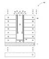
- a semiconductor construction (i.e., integrated structure) 10is shown to comprise a stack 15 of alternating first and second levels 18 and 20 .
- the levels 18are dielectric, and the levels 20 are conductive.
- the conductive levels 20may comprise, for example, one or more of various metals (for example, tungsten, titanium, etc.), metal-containing compositions (for example, metal nitride, metal carbide, metal silicide, etc.), and conductively-doped semiconductor materials (for example, conductively-doped silicon, conductively-doped germanium, etc.).
- the conductive levels 20may comprise n-type doped polycrystalline silicon (i.e., n-type doped polysilicon) of SONOS (semiconductor-oxide-nitride-oxide-semiconductor), or metal of MONOS (metal-oxide-nitride-oxide-semiconductor); with an example MONOS being TANOS (tantalum-alumina-nitride-oxide-semiconductor).
- SONOSsemiconductor-oxide-nitride-oxide-semiconductor
- MONOSmetal-oxide-nitride-oxide-semiconductor
- TANOStantalum-alumina-nitride-oxide-semiconductor
- the dielectric levels 18may comprise any suitable composition or combination of compositions; and may, for example, comprise silicon dioxide.
- the levels 18 and 20may be of any suitable thicknesses; and may, for example, have thicknesses within a range of from about 5 nm to about 300 nm.
- the levels 18may be of different thickness than the levels 20 , or may be the same thickness as the levels 20 .
- the stackis over select device gate material 16 .
- the select device gate material 16may comprise any suitable electrically conductive composition or combination of compositions; and may, for example, comprise conductively-doped semiconductor material, metal and/or metal-containing compositions.
- the select device gate materialis over insulative material 14 .
- Material 14may comprise, for example, one or more oxides; such as, for example, one or more of silicon dioxide, aluminum oxide, hafnium oxide, etc.
- Insulative material 14is over a conductive structure (e.g., line) 11 .
- the conductive structuremay comprise any suitable electrically conductive material; and may, for example, comprise one or more of metal (e.g., copper, titanium, tungsten, etc.), metal-containing composition (e.g., metal carbide, metal nitride, metal silicide, etc.) and conductively-doped semiconductor material (e.g., conductively-doped silicon, conductively-doped germanium, etc.).
- metale.g., copper, titanium, tungsten, etc.
- metal-containing compositione.g., metal carbide, metal nitride, metal silicide, etc.
- conductively-doped semiconductor materiale.g., conductively-doped silicon, conductively-doped germanium, etc.
- insulative material 14is shown between the conductive structure 11 and the select device gate material 16 , in other embodiments there may be multiple insulative materials between the conductive structure and the select device gate material.
- the conductive structure 11is supported by a base 12 .
- a breakis provided between the structure 11 and the base 12 to indicate that there may be additional materials and/or integrated circuit structures between the base and the structure 11 .
- the conductive structure 11may be part of the base (e.g., may be a conductively-doped region of the bulk silicon of a wafer).
- the base 12may comprise semiconductor material; and may, for example, comprise, consist essentially of, or consist of monocrystalline silicon.
- the base 12may be referred to as a semiconductor substrate.
- semiconductor substratemeans any construction comprising semiconductive material, including, but not limited to, bulk semiconductive materials such as a semiconductive wafer (either alone or in assemblies comprising other materials), and semiconductive material layers (either alone or in assemblies comprising other materials).
- substraterefers to any supporting structure, including, but not limited to, the semiconductor substrates described above.
- the base 12may correspond to a semiconductor substrate containing one or more materials associated with integrated circuit fabrication. Such materials may include, for example, one or more of refractory metal materials, barrier materials, diffusion materials, insulator materials, etc.
- An opening 22extends through stack 15 , select device gate material 16 and insulative material 14 .
- the openinghas opposing substantially vertical sidewalls 23 and 25 in the cross-sectional view of FIG. 1 .
- a first dielectric material 24extends vertically adjacent (i.e., along) the sidewalls 23 and 25 ; and is adjacent the conductive levels 20 of stack 15 , as well as adjacent the select device gate material 16 .
- the first dielectric materialmay comprise any suitable composition, and may, for example, comprise silicon dioxide, aluminum oxide (i.e., alumina), hafnium oxide, zirconium oxide, etc.
- the illustrated first dielectric materialbe replaced with two or more materials; with one of the materials being adjacent the bottom of opening 22 (e.g., adjacent select device gate material 16 ), and another of the materials being higher in the opening (e.g., adjacent the conductive levels 20 of stack 15 ). Accordingly, the illustrated dielectric material 24 may be replaced with at least two different dielectric materials in a one-atop-the-other configuration.
- a second dielectric material 26is adjacent the first dielectric material 24 , and is spaced from the conductive levels 20 by the first dielectric material.
- the second dielectric material 26is only within an upper portion of opening 22 , and not within a lower portion of the opening. Specifically, the second dielectric material extends along the conductive levels 20 of stack 15 , but does not extend along the select device gate material 16 .
- the second dielectric materialmay comprise any suitable composition, and may, for example, comprise charge trapping materials, such as silicon nitride, silicon oxynitride, etc.
- a third dielectric material 28is adjacent the second dielectric material 26 , and is spaced from the conductive levels 20 by the first and second dielectric materials.
- the third dielectric material 28is only within the upper portion of opening 22 ; and thus extends along the conductive levels 20 of stack 15 , but not along the select device gate material 16 .
- the third dielectric materialmay comprise any suitable composition, and may, for example, comprise silicon dioxide, aluminum oxide, hafnium oxide, zirconium oxide, etc.
- a channel material 30is adjacent the third dielectric material 28 , and is spaced from the conductive levels 20 by the first, second and third dielectric materials.
- the channel materialalso extends into a bottom of opening 22 along the select device gate material 16 , and is spaced from the select device gate material by the first dielectric material 24 .
- the channel material 30may be considered to be a vertically-extending monolithic channel material, at least as pertains to regions of the channel material adjacent sidewalls 23 and 25 .
- the monolithic channel materialextends vertically along the conductive layers 20 of stack 15 , and along the select device gate material 16 .
- the monolithic channel materialmay be considered to have a lower segment 30 a adjacent the select device gate material, and to have an upper segment 30 b adjacent the conductive levels 20 of stack 15 .
- the dielectric material 24may be considered to be a first material of a first vertically-extending region 32 ; with such first vertically-extending region being between the select device gate material 16 and the lower segment 30 a of the channel material.
- the dielectric materials 24 , 26 and 28may be considered together as forming a second vertically-extending region 34 ; with such second vertically-extending region being between the conductive levels 20 and the upper segment 30 b of the channel material.
- the second vertically-extending region 34has at least one different material than the first vertically extending region 32 , and is horizontally thicker than the first vertically-extending region.
- the channel material 30forms vertically-extending liners adjacent the sidewalls of opening 22 , and an insulator 36 is within a central region of the opening between the vertically-extending liners of material 30 .
- the insulator 36may include gas (for instance, air). Additionally, or alternatively, the insulator may include semisolid or solid material (for instance, silicon dioxide, silicon nitride, etc.).
- the channel material 30may be considered to form a first vertically-extending liner 37 along sidewall 23 of opening 22 , and to form a second vertically-extending liner 39 along the other sidewall 25 of the opening.
- Each vertically extending linermay be considered to have one side contacting insulator 36 , and a second side in opposing relation to said one side; with the second side contacting dielectric materials 24 and 28 .
- the various materials 24 , 26 and 28together with regions of conductive levels 20 and channel material 30 , form a first series of vertically-stacked memory cells 40 a and 40 b , and a second series of vertically-stacked memory cells 41 a and 41 b .
- the vertically-stacked memory cells 40 a and 40 bmay be considered to form a first NAND string
- the vertically-stacked memory cells 41 a and 41 bmay be considered to form a second NAND string.
- the number of memory cells in each NAND stringis determined by the number of conductive levels 20 .
- the stackmay comprise any suitable number of conductive levels.
- the stack 15may comprise 8 conductive levels, 16 conductive levels, 32 conductive levels, 64 conductive levels, 1024 conductive levels, etc.
- the select device gate material 16together with dielectric material 24 and the channel material 30 , forms select devices 42 and 43 .
- Such select devicesmay be source-side select gates (SGS) or drain-side select gates (SGDs).
- the memory cells 40 a , 40 b , 41 a and 41 bare part of a memory array formed over CMOS (complementary-metal-oxide-semiconductor) circuitry.
- the select devices 42 and 43are single-gated MOS (metal-oxide-semiconductor) devices. Such single-gated MOS may advantageously enable utilization of GIDL (gate-induced-drain-leakage) current injection for an erase operation tailored for the CMOS-under-array architecture.
- GIDLgate-induced-drain-leakage
- FIG. 1shows the channel material 30 directly contacting the conductive structure 11 .
- the channel materialmay be spaced from the conductive structure by one or more conductive materials of a conductive plug.
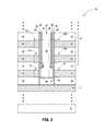
- FIG. 2shows a construction 10 a having a conductive plug 44 .
- the conductive plugis within a bottom region of opening 22 , with an uppermost surface of the plug being beneath the lowestmost conductive level 20 of stack 15 .
- the conductive plugextends along the entirety of the first vertically extending region 32 described above with reference to FIG. 1 , and accordingly the plug has an uppermost surface above select device gate material 16 .
- the conductive plug 44comprises conductive material 46 .
- Such conductive materialmay be homogeneous (as shown) or may comprise two or more different layers.
- the conductive materialmay comprise any suitable composition or combination of compositions; including, for example, one or more of various metals (for example, tungsten, titanium, etc.), metal-containing compositions (for example, metal nitride, metal carbide, metal silicide, etc.), and conductively-doped semiconductor materials (for example, conductively-doped silicon, conductively-doped germanium, etc.).
- the conductive material of structure 11may be referred to as a first conductive material
- the conductive material 46 of the plugmay be referred to as a second conductive material.
- Regions of the conductive material 46 of plug 44are channel material of MOS devices 42 and 43 , and it may be desired that at least such regions comprise semiconductor material (e.g., silicon, germanium, etc.).
- the channel material 30may comprise, consist essentially of, or consist of a first composition; and the conductive material 46 of plug 44 may comprise, consist essentially of, or consist of a second composition.
- the second compositionmay be the same as the first composition (for instance, both may comprise silicon), or the second composition may be different from the first composition (for instance, the second composition may comprise germanium while the first composition comprises silicon; the second composition may comprise silicon and germanium while the first composition consists of silicon, etc.).
- FIG. 3shows another construction ( 10 b ) having a conductive plug 44 between the channel material 30 and the conductive structure 11 .
- the embodiment of FIG. 3differs from that of FIG. 2 in that the conductive plug has an upper surface beneath the select device gate material 16 . Accordingly, the conductive material 46 of the plug is not utilized as channel material of MOS devices 42 and 43 .
- the constructions of FIGS. 1-3may be considered to comprise first channel regions along the conductive levels 20 and second channel regions along the select device gate material 16 .
- the first and second channel regionscomprise a same composition as one another and together form monolithic channel material across the conductive levels and the select device gate material in the constructions of FIGS. 1 and 3 .
- the first and second channel regionsmay comprise different compositions relative to one another in the construction of FIG. 2 (with the first channel region along the select device gate material comprising material 46 , and the second channel region along conductive levels 20 comprising material 30 ).
- a first vertically-extending dielectric regionis between the first channel region and the select device gate material in each of the constructions of FIGS.
- a second vertically-extending dielectric regionis between the second channel region and the conductive levels in each of the constructions of FIGS. 1-3 , with the second vertically-extending dielectric region comprising the vertically-extending materials 24 , 26 and 28 .
- FIGS. 1-3show single select gate devices under vertical strings of memory cells.
- two or more select gate devicesmay be utilized.
- FIG. 4shows a construction 10 c similar to that of FIG. 1 but comprising two vertically-stacked select gate device materials 16 a and 16 b .
- the materials 16 a and 16 bmay be the same composition as one another, or may be of different compositions relative to one another.
- the construction 10 ccomprises dielectric materials 14 a and 14 b ; with material 14 a being between select gate device material 16 a and conductive structure 11 , and with material 14 b separating the select device gate materials from one another.
- the materials 14 a and 14 bmay be the same composition as one another, or may be of different compositions relative to one another.
- FIG. 4is similar to that of FIG. 1 , in that the channel material 30 directly contacts the conductive structure 11 .
- multiple select gate arrangements of the type described with reference to FIG. 4may be utilized in conjunction with conductive plugs 44 of the types described with reference to FIGS. 2 and 3 .
- the vertically-stacked select gate device materialsare incorporated into two sets of vertically-stacked select gate devices; with one set being the devices 42 a and 42 b , and the other set being the devices 43 a and 43 b .
- the devices within each set(for instance, devices 42 a and 42 b ) may be electrically coupled with one another so that they are operated as a single entity, or may be electrically uncoupled relative to one another so that they may be operated separately and independently of one another.
- each set of select devicesis shown comprising two devices in the embodiment of FIG. 4 , in other embodiments the sets may comprise more than two devices.
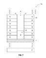
- FIG. 5shows a construction 10 d which more generically illustrates the various arrangements of memory cells and select devices of the embodiment of FIG. 4 .
- the construction 10 dcomprises a vertically-stacked memory region 48 over a select device region 50 .
- the memory regioncomprises a plurality of vertically-stacked memory cells 40 and 41
- the select device regioncomprises a plurality of select devices 42 and 43 .
- the select device regioncomprises vertically-stacked conductive levels 16 , alternating with vertically-stacked insulative levels 14 .
- At least two of the conductive levels 16may comprise a same composition as one another and/or at least two of the conductive levels 16 may comprise a different composition relative to one another.
- at least two of the insulative levels 14may comprise a same composition as one another and/or at least two of the insulative levels 14 may comprise a different composition relative to one another.
- Channel material 30extends monolithically through the vertically-stacked memory region and through the select device region.
- the channel materialcomprises a first (lower) segment 30 a spaced from the conductive levels 16 of the select device region by first vertically-extending region 32 , and comprises a second (upper) segment 30 b spaced from conductive levels 20 of the vertically-stacked memory region by second vertically-extending region 34 .
- the vertically-extending regions 32 and 34may comprise dielectric materials (for instance, the dielectric materials 24 , 26 and 28 described above with reference to FIGS. 1-4 ).
- region 34is horizontally thicker than the region 32 due to region 34 comprising more materials than region 32 (for instance, region 34 may comprise the vertically-extending materials 24 , 26 and 28 , while region 32 comprises only the vertically-extending material 24 ; as shown in FIG. 1 ).
- the select device regioncomprises two sets of vertically-stacked select devices (with one set comprising devices 42 , and the other set comprising devices 43 ). Each set is shown comprising two devices, but broken lines are provided within the select device region to indicate that there may be more than the illustrated number of devices within each set. For instance, in some embodiments there may be three select devices with each set, four select devices within each set, etc. If multiple select devices are within a vertically-extending set, at least two of the devices may be electrically coupled with one another and utilized as a common unit and/or at least two of the devices may be operated separately and independently of one another.
- FIG. 5is similar to that of FIG. 1 , in that the channel material 30 directly contacts the conductive structure 11 .
- the arrangement of FIG. 5may be utilized in conjunction with conductive plugs 44 of the types described with reference to FIGS. 2 and 3 .
- FIGS. 1-5show channel material 30 configured as a liner which partially fills opening 22 to leave a hollow within the opening (with such hollow being filled with insulator 36 ), in other embodiments the channel material may entirely fill opening 22 .
- FIGS. 1-5be formed utilizing any suitable processing.
- Example processingis described with reference to FIGS. 6-13 .
- a construction 10 ecomprises a stack 60 with alternating levels 62 and 63 .
- the levels 62 and 63may be identical to the levels 18 and 20 of FIG. 1 , or may be different.
- the constructionalso comprises a material 64 over conductive structure 11 , and a material 65 over the material 64 .
- the materials 64 and 65may be the same as materials 14 and 16 of FIG. 1 , or may be different.
- Opening 22is formed through materials 62 , 63 , 64 and 65 , and the sidewalls of the opening are lined with dielectric material 24 .
- the material 24does not extend across a bottom of opening 22 .
- Such configurationmay be achieved by, for example, utilizing an anisotropic etch after deposition of material 24 .
- material 66is provided at a bottom of opening 22 to form a plug 68 .
- the material 66may be a same composition as the material 46 described above with reference to FIG. 2 , or may be different.
- material 66is sacrificial, and accordingly may comprise anything suitable for being deposited and removed relative to other materials of construction 10 e .
- material 66becomes the plug 44 of FIGS. 2 and 3 , and accordingly may comprise any of the conductive compositions described above as being suitable for such plug.
- materials 26 and 28are deposited within opening 22 , and a protective spacer 70 is formed along material 28 .
- the protective spacermay comprise any suitable composition.
- the protective spacerextends along vertical sidewalls of opening 22 , but not along a bottom of the opening.
- the protective spacermay be formed in such configuration utilizing anisotropic etching subsequent to deposition of material of spacer 70 .
- the spacer 70together with materials 24 , 26 and 28 , narrows the opening 22 .
- the narrowed openingis extended through materials 26 and 28 with one or more etches.
- the extension of the narrowed opening through materials 26 and 28exposes plug material 66 .
- protective material 70 and plug material 66are removed.
- the protective material and plug materialcomprise a same composition as one another to simplify the removal of such materials.
- the protective material and plug materialboth comprise silicon.
- channel material 30is formed within opening 22 .
- Insulator 36is also shown within the opening. If the insulator is simply air, then the insulator does not have to be separately provided after formation of channel material 30 . If instead the insulator is dielectric material (for instance, silicon dioxide), the dielectric material may be provided with a deposition following the deposit of material 30 .
- dielectric materialfor instance, silicon dioxide
- FIG. 11may be identical to that of FIG. 1 if the materials 62 and 63 are the same as materials 18 and 20 of FIG. 1 , and if materials 64 and 65 are the same as materials 14 and 16 of FIG. 1 .
- materials 65 and 63may correspond to a sacrificial material which is ultimately replaced with conductive material corresponding to the conductive levels 16 and 20 of FIG. 1 .
- the material 65 and 63may be replaced with tantalum-containing material to form metal-containing conductive levels 16 and 20 in some embodiments.
- FIG. 10shows plug material 66 ( FIG. 9 ) entirely removed.
- the plug materialmay remain, and be incorporated into a construction of the type shown in FIG. 2 or of the type shown in FIG. 3 .
- FIG. 12shows an alternative processing stage to that of FIG. 10 , and shows some of the plug material 66 remaining as a plug 68 .
- FIG. 13shows a processing stage subsequent to that of FIG. 12 , and shows the channel material 30 and insulator 36 formed within opening 22 .
- the construction of FIG. 13may be identical to that of FIG. 3 if the materials 62 and 63 are the same as the materials 18 and 20 of FIG. 3 , if materials 64 and 65 are the same as materials 14 and 16 of FIG. 3 , and if the plug material 66 is the same as the plug material 46 of FIG. 3 .
- materials 65 and 63may correspond to sacrificial material which is ultimately replaced with conductive materials corresponding to the levels 16 and 20 of FIG. 3 .
- the structures described abovemay be incorporated into electronic systems.
- Such electronic systemsmay be used in, for example, memory modules, device drivers, power modules, communication modems, processor modules, and application-specific modules, and may include multilayer, multichip modules.
- the electronic systemsmay be any of a broad range of systems, such as, for example, cameras, wireless devices, displays, chip sets, set top boxes, games, lighting, vehicles, clocks, televisions, cell phones, personal computers, automobiles, industrial control systems, aircraft, etc.
- the various materials, substances, compositions, etc. described hereinmay be formed with any suitable methodologies, either now known or yet to be developed, including, for example, atomic layer deposition (ALD), chemical vapor deposition (CVD), physical vapor deposition (PVD), etc.
- ALDatomic layer deposition
- CVDchemical vapor deposition
- PVDphysical vapor deposition
- dielectricdielectric
- electrically insulativedielectrically insulative
- the termsare considered synonymous in this disclosure.
- the utilization of the term “dielectric” in some instances, and the term “electrically insulative” in other instances,may be to provide language variation within this disclosure to simplify antecedent basis within the claims that follow, and is not utilized to indicate any significant chemical or electrical differences.
- Some embodimentsinclude an integrated structure having a conductive material, a select device gate material over the conductive material and spaced from the conductive material by one or more insulative materials, and vertically-stacked conductive levels over the select device gate material.
- Vertically-extending monolithic channel materialis adjacent the select device gate material and the conductive levels.
- the monolithic channel materialcontains a lower segment along the select device gate material and an upper segment along the conductive levels.
- a first vertically-extending regionis between the lower segment of the monolithic channel material and the select device gate material.
- the first vertically-extending regioncontains a first material.
- a second vertically-extending regionis between the upper segment of the monolithic channel material and the conductive levels.
- the second vertically-extending regioncontains one or more vertically-extending materials which are different in composition from the first material.
- Some embodimentsinclude an integrated structure having a conductive material, two or more select devices over the conductive material, and vertically-stacked conductive levels over the select devices.
- Vertically-extending monolithic channel materialcontains a lower segment adjacent the select devices and an upper segment adjacent the conductive levels.
- a first vertically-extending regionis between the lower segment of the monolithic channel material and gates of the select devices.
- the first vertically-extending regioncomprises a first material.
- a second vertically-extending regionis between the upper segment of the monolithic channel material and the conductive levels.
- the second vertically-extending regioncomprises one or more vertically-extending materials which are different in composition from the first material.
- Some embodimentsinclude an integrated structure having a conductive material, a select device gate material over the conductive material and spaced from the conductive material by one or more insulative materials, and vertically-stacked conductive levels over the select device gate material.
- the conductive levelsare spaced from one another by intervening dielectric levels and comprise metal.
- An openingextends through the conductive levels and the select device gate material.
- the openinghas substantially vertical sidewalls which extend adjacent the conductive levels and adjacent the select device gate material.
- Channel materialis adjacent the sidewalls of the opening.
- the channel materialis horizontally spaced from the select device gate material by a first dielectric region, and is horizontally spaced from the conductive levels by a second dielectric region which is compositionally different from the first dielectric region.
- Some embodimentsinclude an integrated structure comprising vertically-stacked metal-containing conductive levels over a metal-containing select device gate material.
- a first channel regionis adjacent the select device gate material, and a second channel region is adjacent the conductive levels.
- a first vertically-extending dielectric regionis between the first channel region and the select device gate material, with the first vertically-extending dielectric region comprising a first material.
- a second vertically-extending dielectric regionis between the second channel region and the conductive levels, with the second vertically-extending dielectric region comprising a vertically-extending material which is different in composition from the first material.
Landscapes
- Semiconductor Memories (AREA)
- Non-Volatile Memory (AREA)
Abstract
Description
- Integrated structures having vertically-stacked conductive levels over select devices.
- Memory provides data storage for electronic systems. Flash memory is one type of memory, and has numerous uses in modern computers and devices. For instance, modern personal computers may have BIOS stored on a flash memory chip. As another example, it is becoming increasingly common for computers and other devices to utilize flash memory in solid state drives to replace conventional hard drives. As yet another example, flash memory is popular in wireless electronic devices because it enables manufacturers to support new communication protocols as they become standardized, and to provide the ability to remotely upgrade the devices for enhanced features.
- NAND may be a basic architecture of integrated flash memory. A NAND cell unit comprises at least one selecting device coupled in series to a serial combination of memory cells (with the serial combination commonly being referred to as a NAND string). NAND architecture may be configured to comprise vertically-stacked memory cells. It is desired to develop improved NAND architecture, and improved methods of forming NAND architecture.
FIGS. 1-5 are diagrammatic cross-sectional views of example embodiment integrated structures.FIGS. 6-11 are diagrammatic cross-sectional views of example embodiment process stages utilized in fabricating an example embodiment integrated structure.FIGS. 12 and 13 are diagrammatic cross-sectional views of example embodiment process stages utilized in fabricating another example embodiment integrated structure. The process stage ofFIG. 12 may follow that ofFIG. 9 .- In some embodiments, integrated structures comprise monolithic channel material adjacent (or along) at least one select device and adjacent (or along) vertically-stacked memory cells over the select device. Example embodiments are described with reference to
FIGS. 1-13 . - Referring to
FIG. 1 , a semiconductor construction (i.e., integrated structure)10 is shown to comprise astack 15 of alternating first andsecond levels levels 18 are dielectric, and thelevels 20 are conductive. Theconductive levels 20 may comprise, for example, one or more of various metals (for example, tungsten, titanium, etc.), metal-containing compositions (for example, metal nitride, metal carbide, metal silicide, etc.), and conductively-doped semiconductor materials (for example, conductively-doped silicon, conductively-doped germanium, etc.). For instance, theconductive levels 20 may comprise n-type doped polycrystalline silicon (i.e., n-type doped polysilicon) of SONOS (semiconductor-oxide-nitride-oxide-semiconductor), or metal of MONOS (metal-oxide-nitride-oxide-semiconductor); with an example MONOS being TANOS (tantalum-alumina-nitride-oxide-semiconductor). - The
dielectric levels 18 may comprise any suitable composition or combination of compositions; and may, for example, comprise silicon dioxide. - The
levels levels 18 may be of different thickness than thelevels 20, or may be the same thickness as thelevels 20. - The stack is over select
device gate material 16. The selectdevice gate material 16 may comprise any suitable electrically conductive composition or combination of compositions; and may, for example, comprise conductively-doped semiconductor material, metal and/or metal-containing compositions. - The select device gate material is over
insulative material 14.Material 14 may comprise, for example, one or more oxides; such as, for example, one or more of silicon dioxide, aluminum oxide, hafnium oxide, etc. Insulative material 14 is over a conductive structure (e.g., line)11. The conductive structure may comprise any suitable electrically conductive material; and may, for example, comprise one or more of metal (e.g., copper, titanium, tungsten, etc.), metal-containing composition (e.g., metal carbide, metal nitride, metal silicide, etc.) and conductively-doped semiconductor material (e.g., conductively-doped silicon, conductively-doped germanium, etc.).- Although one
insulative material 14 is shown between theconductive structure 11 and the selectdevice gate material 16, in other embodiments there may be multiple insulative materials between the conductive structure and the select device gate material. - The
conductive structure 11 is supported by abase 12. A break is provided between thestructure 11 and thebase 12 to indicate that there may be additional materials and/or integrated circuit structures between the base and thestructure 11. Also, it is to be understood that in some embodiments theconductive structure 11 may be part of the base (e.g., may be a conductively-doped region of the bulk silicon of a wafer). - The
base 12 may comprise semiconductor material; and may, for example, comprise, consist essentially of, or consist of monocrystalline silicon. Thebase 12 may be referred to as a semiconductor substrate. The term “semiconductor substrate” means any construction comprising semiconductive material, including, but not limited to, bulk semiconductive materials such as a semiconductive wafer (either alone or in assemblies comprising other materials), and semiconductive material layers (either alone or in assemblies comprising other materials). The term “substrate” refers to any supporting structure, including, but not limited to, the semiconductor substrates described above. In some applications, thebase 12 may correspond to a semiconductor substrate containing one or more materials associated with integrated circuit fabrication. Such materials may include, for example, one or more of refractory metal materials, barrier materials, diffusion materials, insulator materials, etc. - An
opening 22 extends throughstack 15, selectdevice gate material 16 andinsulative material 14. The opening has opposing substantiallyvertical sidewalls FIG. 1 . - A first
dielectric material 24 extends vertically adjacent (i.e., along) thesidewalls conductive levels 20 ofstack 15, as well as adjacent the selectdevice gate material 16. The first dielectric material may comprise any suitable composition, and may, for example, comprise silicon dioxide, aluminum oxide (i.e., alumina), hafnium oxide, zirconium oxide, etc. In some embodiments (not shown), the illustrated first dielectric material be replaced with two or more materials; with one of the materials being adjacent the bottom of opening22 (e.g., adjacent select device gate material16), and another of the materials being higher in the opening (e.g., adjacent theconductive levels 20 of stack15). Accordingly, the illustrateddielectric material 24 may be replaced with at least two different dielectric materials in a one-atop-the-other configuration. - A second
dielectric material 26 is adjacent the firstdielectric material 24, and is spaced from theconductive levels 20 by the first dielectric material. The seconddielectric material 26 is only within an upper portion of opening22, and not within a lower portion of the opening. Specifically, the second dielectric material extends along theconductive levels 20 ofstack 15, but does not extend along the selectdevice gate material 16. The second dielectric material may comprise any suitable composition, and may, for example, comprise charge trapping materials, such as silicon nitride, silicon oxynitride, etc. - A third
dielectric material 28 is adjacent the seconddielectric material 26, and is spaced from theconductive levels 20 by the first and second dielectric materials. The thirddielectric material 28 is only within the upper portion of opening22; and thus extends along theconductive levels 20 ofstack 15, but not along the selectdevice gate material 16. The third dielectric material may comprise any suitable composition, and may, for example, comprise silicon dioxide, aluminum oxide, hafnium oxide, zirconium oxide, etc. - A
channel material 30 is adjacent the thirddielectric material 28, and is spaced from theconductive levels 20 by the first, second and third dielectric materials. The channel material also extends into a bottom of opening22 along the selectdevice gate material 16, and is spaced from the select device gate material by the firstdielectric material 24. - In some embodiments, the
channel material 30 may be considered to be a vertically-extending monolithic channel material, at least as pertains to regions of the channel materialadjacent sidewalls conductive layers 20 ofstack 15, and along the selectdevice gate material 16. The monolithic channel material may be considered to have alower segment 30aadjacent the select device gate material, and to have anupper segment 30badjacent theconductive levels 20 ofstack 15. Thedielectric material 24 may be considered to be a first material of a first vertically-extendingregion 32; with such first vertically-extending region being between the selectdevice gate material 16 and thelower segment 30aof the channel material. Similarly, thedielectric materials region 34; with such second vertically-extending region being between theconductive levels 20 and theupper segment 30bof the channel material. - In the embodiment of
FIG. 1 , the second vertically-extendingregion 34 has at least one different material than the first vertically extendingregion 32, and is horizontally thicker than the first vertically-extending region. - The
channel material 30 forms vertically-extending liners adjacent the sidewalls of opening22, and aninsulator 36 is within a central region of the opening between the vertically-extending liners ofmaterial 30. Theinsulator 36 may include gas (for instance, air). Additionally, or alternatively, the insulator may include semisolid or solid material (for instance, silicon dioxide, silicon nitride, etc.). In some embodiments, thechannel material 30 may be considered to form a first vertically-extendingliner 37 alongsidewall 23 ofopening 22, and to form a second vertically-extendingliner 39 along theother sidewall 25 of the opening. Each vertically extending liner may be considered to have oneside contacting insulator 36, and a second side in opposing relation to said one side; with the second side contactingdielectric materials - The
various materials conductive levels 20 andchannel material 30, form a first series of vertically-stackedmemory cells memory cells memory cells memory cells - The number of memory cells in each NAND string is determined by the number of
conductive levels 20. The stack may comprise any suitable number of conductive levels. In some embodiments, thestack 15 may comprise 8 conductive levels, 16 conductive levels, 32 conductive levels, 64 conductive levels, 1024 conductive levels, etc. - The select
device gate material 16, together withdielectric material 24 and thechannel material 30, forms selectdevices memory cells select devices - The embodiment of
FIG. 1 shows thechannel material 30 directly contacting theconductive structure 11. In other embodiments the channel material may be spaced from the conductive structure by one or more conductive materials of a conductive plug. For instance,FIG. 2 shows aconstruction 10ahaving aconductive plug 44. The conductive plug is within a bottom region of opening22, with an uppermost surface of the plug being beneath the lowestmostconductive level 20 ofstack 15. In the embodiment ofFIG. 2 , the conductive plug extends along the entirety of the first vertically extendingregion 32 described above with reference toFIG. 1 , and accordingly the plug has an uppermost surface above selectdevice gate material 16. - The
conductive plug 44 comprisesconductive material 46. Such conductive material may be homogeneous (as shown) or may comprise two or more different layers. The conductive material may comprise any suitable composition or combination of compositions; including, for example, one or more of various metals (for example, tungsten, titanium, etc.), metal-containing compositions (for example, metal nitride, metal carbide, metal silicide, etc.), and conductively-doped semiconductor materials (for example, conductively-doped silicon, conductively-doped germanium, etc.). In some embodiments, the conductive material ofstructure 11 may be referred to as a first conductive material, and theconductive material 46 of the plug may be referred to as a second conductive material. - Regions of the
conductive material 46 ofplug 44 are channel material ofMOS devices - In some embodiments, the
channel material 30 may comprise, consist essentially of, or consist of a first composition; and theconductive material 46 ofplug 44 may comprise, consist essentially of, or consist of a second composition. The second composition may be the same as the first composition (for instance, both may comprise silicon), or the second composition may be different from the first composition (for instance, the second composition may comprise germanium while the first composition comprises silicon; the second composition may comprise silicon and germanium while the first composition consists of silicon, etc.). FIG. 3 shows another construction (10b) having aconductive plug 44 between thechannel material 30 and theconductive structure 11. The embodiment ofFIG. 3 differs from that ofFIG. 2 in that the conductive plug has an upper surface beneath the selectdevice gate material 16. Accordingly, theconductive material 46 of the plug is not utilized as channel material ofMOS devices - In some embodiments, the constructions of
FIGS. 1-3 may be considered to comprise first channel regions along theconductive levels 20 and second channel regions along the selectdevice gate material 16. The first and second channel regions comprise a same composition as one another and together form monolithic channel material across the conductive levels and the select device gate material in the constructions ofFIGS. 1 and 3 . In contrast, the first and second channel regions may comprise different compositions relative to one another in the construction ofFIG. 2 (with the first channel region along the select device gatematerial comprising material 46, and the second channel region alongconductive levels 20 comprising material30). A first vertically-extending dielectric region is between the first channel region and the select device gate material in each of the constructions ofFIGS. 1-3 , with the first vertically-extending dielectric region comprising thematerial 24. Also, a second vertically-extending dielectric region is between the second channel region and the conductive levels in each of the constructions ofFIGS. 1-3 , with the second vertically-extending dielectric region comprising the vertically-extendingmaterials - The embodiments of
FIGS. 1-3 show single select gate devices under vertical strings of memory cells. In other embodiments, two or more select gate devices may be utilized. For instance,FIG. 4 shows aconstruction 10csimilar to that ofFIG. 1 but comprising two vertically-stacked selectgate device materials materials - The
construction 10ccomprisesdielectric materials material 14abeing between selectgate device material 16aandconductive structure 11, and withmaterial 14bseparating the select device gate materials from one another. Thematerials - The embodiment of
FIG. 4 is similar to that ofFIG. 1 , in that thechannel material 30 directly contacts theconductive structure 11. In other embodiments, multiple select gate arrangements of the type described with reference toFIG. 4 may be utilized in conjunction withconductive plugs 44 of the types described with reference toFIGS. 2 and 3 . - The vertically-stacked select gate device materials are incorporated into two sets of vertically-stacked select gate devices; with one set being the
devices devices devices FIG. 4 , in other embodiments the sets may comprise more than two devices.FIG. 5 shows aconstruction 10dwhich more generically illustrates the various arrangements of memory cells and select devices of the embodiment ofFIG. 4 . - The
construction 10dcomprises a vertically-stackedmemory region 48 over aselect device region 50. The memory region comprises a plurality of vertically-stackedmemory cells select devices conductive levels 16, alternating with vertically-stackedinsulative levels 14. At least two of theconductive levels 16 may comprise a same composition as one another and/or at least two of theconductive levels 16 may comprise a different composition relative to one another. Also, at least two of theinsulative levels 14 may comprise a same composition as one another and/or at least two of theinsulative levels 14 may comprise a different composition relative to one another. Channel material 30 extends monolithically through the vertically-stacked memory region and through the select device region. The channel material comprises a first (lower)segment 30aspaced from theconductive levels 16 of the select device region by first vertically-extendingregion 32, and comprises a second (upper)segment 30bspaced fromconductive levels 20 of the vertically-stacked memory region by second vertically-extendingregion 34. The vertically-extendingregions dielectric materials FIGS. 1-4 ). Theregion 34 is horizontally thicker than theregion 32 due toregion 34 comprising more materials than region32 (for instance,region 34 may comprise the vertically-extendingmaterials region 32 comprises only the vertically-extendingmaterial 24; as shown inFIG. 1 ).- The select device region comprises two sets of vertically-stacked select devices (with one
set comprising devices 42, and the other set comprising devices43). Each set is shown comprising two devices, but broken lines are provided within the select device region to indicate that there may be more than the illustrated number of devices within each set. For instance, in some embodiments there may be three select devices with each set, four select devices within each set, etc. If multiple select devices are within a vertically-extending set, at least two of the devices may be electrically coupled with one another and utilized as a common unit and/or at least two of the devices may be operated separately and independently of one another. - The embodiment of
FIG. 5 is similar to that ofFIG. 1 , in that thechannel material 30 directly contacts theconductive structure 11. In other embodiments, the arrangement ofFIG. 5 may be utilized in conjunction withconductive plugs 44 of the types described with reference toFIGS. 2 and 3 . - Although the embodiments of
FIGS. 1-5 show channel material 30 configured as a liner which partially fills opening22 to leave a hollow within the opening (with such hollow being filled with insulator36), in other embodiments the channel material may entirely fillopening 22. - The structures described with reference to
FIGS. 1-5 be formed utilizing any suitable processing. Example processing is described with reference toFIGS. 6-13 . - Referring to
FIG. 6 , aconstruction 10ecomprises astack 60 with alternatinglevels levels levels FIG. 1 , or may be different. - The construction also comprises a material64 over
conductive structure 11, and a material65 over thematerial 64. Thematerials materials FIG. 1 , or may be different. Opening 22 is formed throughmaterials dielectric material 24. Thematerial 24 does not extend across a bottom ofopening 22. Such configuration may be achieved by, for example, utilizing an anisotropic etch after deposition ofmaterial 24.- Referring to
FIG. 7 ,material 66 is provided at a bottom of opening22 to form aplug 68. Thematerial 66 may be a same composition as thematerial 46 described above with reference toFIG. 2 , or may be different. In some embodiments,material 66 is sacrificial, and accordingly may comprise anything suitable for being deposited and removed relative to other materials ofconstruction 10e. In other embodiments,material 66 becomes theplug 44 ofFIGS. 2 and 3 , and accordingly may comprise any of the conductive compositions described above as being suitable for such plug. - Referring to
FIG. 8 ,materials protective spacer 70 is formed alongmaterial 28. The protective spacer may comprise any suitable composition. The protective spacer extends along vertical sidewalls of opening22, but not along a bottom of the opening. The protective spacer may be formed in such configuration utilizing anisotropic etching subsequent to deposition of material ofspacer 70. - The
spacer 70, together withmaterials opening 22. - Referring to
FIG. 9 , the narrowed opening is extended throughmaterials materials material 66. - Referring to
FIG. 10 ,protective material 70 and plug material66 (FIG. 9 ) are removed. In some embodiments, the protective material and plug material comprise a same composition as one another to simplify the removal of such materials. For instance, in some embodiments the protective material and plug material both comprise silicon. - Referring to
FIG. 11 ,channel material 30 is formed withinopening 22.Insulator 36 is also shown within the opening. If the insulator is simply air, then the insulator does not have to be separately provided after formation ofchannel material 30. If instead the insulator is dielectric material (for instance, silicon dioxide), the dielectric material may be provided with a deposition following the deposit ofmaterial 30. - The construction of
FIG. 11 may be identical to that ofFIG. 1 if thematerials materials FIG. 1 , and ifmaterials materials FIG. 1 . However, in someembodiments materials conductive levels FIG. 1 . For instance, thematerial conductive levels - The processing stage of
FIG. 10 shows plug material66 (FIG. 9 ) entirely removed. In other embodiments, the plug material may remain, and be incorporated into a construction of the type shown inFIG. 2 or of the type shown inFIG. 3 . For instance,FIG. 12 shows an alternative processing stage to that ofFIG. 10 , and shows some of theplug material 66 remaining as aplug 68. FIG. 13 shows a processing stage subsequent to that ofFIG. 12 , and shows thechannel material 30 andinsulator 36 formed withinopening 22. The construction ofFIG. 13 may be identical to that ofFIG. 3 if thematerials materials FIG. 3 , ifmaterials materials FIG. 3 , and if theplug material 66 is the same as theplug material 46 ofFIG. 3 . In some embodiments,materials levels FIG. 3 .- The structures described above may be incorporated into electronic systems. Such electronic systems may be used in, for example, memory modules, device drivers, power modules, communication modems, processor modules, and application-specific modules, and may include multilayer, multichip modules. The electronic systems may be any of a broad range of systems, such as, for example, cameras, wireless devices, displays, chip sets, set top boxes, games, lighting, vehicles, clocks, televisions, cell phones, personal computers, automobiles, industrial control systems, aircraft, etc.
- Unless specified otherwise, the various materials, substances, compositions, etc. described herein may be formed with any suitable methodologies, either now known or yet to be developed, including, for example, atomic layer deposition (ALD), chemical vapor deposition (CVD), physical vapor deposition (PVD), etc.
- Both of the terms “dielectric” and “electrically insulative” may be utilized to describe materials having insulative electrical properties. The terms are considered synonymous in this disclosure. The utilization of the term “dielectric” in some instances, and the term “electrically insulative” in other instances, may be to provide language variation within this disclosure to simplify antecedent basis within the claims that follow, and is not utilized to indicate any significant chemical or electrical differences.
- The particular orientation of the various embodiments in the drawings is for illustrative purposes only, and the embodiments may be rotated relative to the shown orientations in some applications. The description provided herein, and the claims that follow, pertain to any structures that have the described relationships between various features, regardless of whether the structures are in the particular orientation of the drawings, or are rotated relative to such orientation.
- The cross-sectional views of the accompanying illustrations only show features within the planes of the cross-sections, and do not show materials behind the planes of the cross-sections in order to simplify the drawings.
- When a structure is referred to above as being “on” or “against” another structure, it can be directly on the other structure or intervening structures may also be present. In contrast, when a structure is referred to as being “directly on” or “directly against” another structure, there are no intervening structures present. When a structure is referred to as being “connected” or “coupled” to another structure, it can be directly connected or coupled to the other structure, or intervening structures may be present. In contrast, when a structure is referred to as being “directly connected” or “directly coupled” to another structure, there are no intervening structures present.
- Some embodiments include an integrated structure having a conductive material, a select device gate material over the conductive material and spaced from the conductive material by one or more insulative materials, and vertically-stacked conductive levels over the select device gate material. Vertically-extending monolithic channel material is adjacent the select device gate material and the conductive levels. The monolithic channel material contains a lower segment along the select device gate material and an upper segment along the conductive levels. A first vertically-extending region is between the lower segment of the monolithic channel material and the select device gate material. The first vertically-extending region contains a first material. A second vertically-extending region is between the upper segment of the monolithic channel material and the conductive levels. The second vertically-extending region contains one or more vertically-extending materials which are different in composition from the first material.
- Some embodiments include an integrated structure having a conductive material, two or more select devices over the conductive material, and vertically-stacked conductive levels over the select devices. Vertically-extending monolithic channel material contains a lower segment adjacent the select devices and an upper segment adjacent the conductive levels. A first vertically-extending region is between the lower segment of the monolithic channel material and gates of the select devices. The first vertically-extending region comprises a first material. A second vertically-extending region is between the upper segment of the monolithic channel material and the conductive levels. The second vertically-extending region comprises one or more vertically-extending materials which are different in composition from the first material.
- Some embodiments include an integrated structure having a conductive material, a select device gate material over the conductive material and spaced from the conductive material by one or more insulative materials, and vertically-stacked conductive levels over the select device gate material. The conductive levels are spaced from one another by intervening dielectric levels and comprise metal. An opening extends through the conductive levels and the select device gate material. The opening has substantially vertical sidewalls which extend adjacent the conductive levels and adjacent the select device gate material. Channel material is adjacent the sidewalls of the opening. The channel material is horizontally spaced from the select device gate material by a first dielectric region, and is horizontally spaced from the conductive levels by a second dielectric region which is compositionally different from the first dielectric region.
- Some embodiments include an integrated structure comprising vertically-stacked metal-containing conductive levels over a metal-containing select device gate material. A first channel region is adjacent the select device gate material, and a second channel region is adjacent the conductive levels. A first vertically-extending dielectric region is between the first channel region and the select device gate material, with the first vertically-extending dielectric region comprising a first material. A second vertically-extending dielectric region is between the second channel region and the conductive levels, with the second vertically-extending dielectric region comprising a vertically-extending material which is different in composition from the first material.
- In compliance with the statute, the subject matter disclosed herein has been described in language more or less specific as to structural and methodical features. It is to be understood, however, that the claims are not limited to the specific features shown and described, since the means herein disclosed comprise example embodiments. The claims are thus to be afforded full scope as literally worded, and to be appropriately interpreted in accordance with the doctrine of equivalents.
Claims (26)
Priority Applications (7)
| Application Number | Priority Date | Filing Date | Title |
|---|---|---|---|
| US14/830,517US9741732B2 (en) | 2015-08-19 | 2015-08-19 | Integrated structures |
| US15/651,719US10256249B2 (en) | 2015-08-19 | 2017-07-17 | Integrated structures |
| US16/290,169US10355018B1 (en) | 2015-08-19 | 2019-03-01 | Integrated structures |
| US16/438,334US11081495B2 (en) | 2015-08-19 | 2019-06-11 | Integrated structures |
| US17/378,743US12185537B2 (en) | 2015-08-19 | 2021-07-18 | Integrated structures |
| US18/966,391US20250098169A1 (en) | 2015-08-19 | 2024-12-03 | Integrated Structures |
| US19/009,758US20250142827A1 (en) | 2015-08-19 | 2025-01-03 | Integrated Structures |
Applications Claiming Priority (1)
| Application Number | Priority Date | Filing Date | Title |
|---|---|---|---|
| US14/830,517US9741732B2 (en) | 2015-08-19 | 2015-08-19 | Integrated structures |
Related Child Applications (1)
| Application Number | Title | Priority Date | Filing Date |
|---|---|---|---|
| US15/651,719ContinuationUS10256249B2 (en) | 2015-08-19 | 2017-07-17 | Integrated structures |
Publications (2)
| Publication Number | Publication Date |
|---|---|
| US20170054036A1true US20170054036A1 (en) | 2017-02-23 |
| US9741732B2 US9741732B2 (en) | 2017-08-22 |
Family
ID=58158430
Family Applications (7)
| Application Number | Title | Priority Date | Filing Date |
|---|---|---|---|
| US14/830,517Active2035-10-14US9741732B2 (en) | 2015-08-19 | 2015-08-19 | Integrated structures |
| US15/651,719ActiveUS10256249B2 (en) | 2015-08-19 | 2017-07-17 | Integrated structures |
| US16/290,169ActiveUS10355018B1 (en) | 2015-08-19 | 2019-03-01 | Integrated structures |
| US16/438,334Active2035-08-30US11081495B2 (en) | 2015-08-19 | 2019-06-11 | Integrated structures |
| US17/378,743Active2037-05-24US12185537B2 (en) | 2015-08-19 | 2021-07-18 | Integrated structures |
| US18/966,391PendingUS20250098169A1 (en) | 2015-08-19 | 2024-12-03 | Integrated Structures |
| US19/009,758PendingUS20250142827A1 (en) | 2015-08-19 | 2025-01-03 | Integrated Structures |
Family Applications After (6)
| Application Number | Title | Priority Date | Filing Date |
|---|---|---|---|
| US15/651,719ActiveUS10256249B2 (en) | 2015-08-19 | 2017-07-17 | Integrated structures |
| US16/290,169ActiveUS10355018B1 (en) | 2015-08-19 | 2019-03-01 | Integrated structures |
| US16/438,334Active2035-08-30US11081495B2 (en) | 2015-08-19 | 2019-06-11 | Integrated structures |
| US17/378,743Active2037-05-24US12185537B2 (en) | 2015-08-19 | 2021-07-18 | Integrated structures |
| US18/966,391PendingUS20250098169A1 (en) | 2015-08-19 | 2024-12-03 | Integrated Structures |
| US19/009,758PendingUS20250142827A1 (en) | 2015-08-19 | 2025-01-03 | Integrated Structures |
Country Status (1)
| Country | Link |
|---|---|
| US (7) | US9741732B2 (en) |
Cited By (26)
| Publication number | Priority date | Publication date | Assignee | Title |
|---|---|---|---|---|
| US10186521B2 (en)* | 2016-09-16 | 2019-01-22 | Toshiba Memory Corporation | Semiconductor device and method for manufacturing semiconductor device |
| US10636808B2 (en) | 2017-07-13 | 2020-04-28 | Samsung Electronics Co., Ltd. | Vertical memory device having an epitaxial layer in contact with a channel layer |
| US20200266203A1 (en)* | 2019-02-15 | 2020-08-20 | Micron Technology, Inc. | Memory Arrays And Methods Used In Forming A Memory Array |
| US11075215B2 (en) | 2019-01-18 | 2021-07-27 | Micron Technology, Inc. | Memory arrays and methods used in forming a memory array |
| US11121145B1 (en) | 2020-03-03 | 2021-09-14 | Micron Technology, Inc. | Memory arrays comprising strings of memory cells and methods used in forming a memory array comprising strings of memory cells |
| US11139386B2 (en) | 2020-03-03 | 2021-10-05 | Micron Technology, Inc. | Memory arrays comprising strings of memory cells and methods used in forming a memory array comprising strings of memory cells |
| US11251190B2 (en) | 2020-05-13 | 2022-02-15 | Micron Technology, Inc. | Memory arrays comprising strings of memory cells and methods used in forming a memory array comprising strings of memory cells |
| US11257839B2 (en) | 2020-05-12 | 2022-02-22 | Micron Technology, Inc. | Memory arrays comprising strings of memory cells and methods used in forming a memory array comprising strings of memory cells |
| US11282847B2 (en) | 2020-05-13 | 2022-03-22 | Micron Technology, Inc. | Methods used in forming a memory array comprising strings of memory cells |
| US11282815B2 (en) | 2020-01-14 | 2022-03-22 | Micron Technology, Inc. | Methods of forming microelectronic devices, and related microelectronic devices and electronic systems |
| US11335602B2 (en) | 2020-06-18 | 2022-05-17 | Micron Technology, Inc. | Methods of forming microelectronic devices, and related microelectronic devices and electronic systems |
| US11380669B2 (en) | 2020-06-18 | 2022-07-05 | Micron Technology, Inc. | Methods of forming microelectronic devices |
| US11387243B2 (en) | 2020-05-13 | 2022-07-12 | Micron Technology, Inc. | Memory arrays comprising strings of memory cells and methods used in forming a memory array comprising strings of memory cells |
| US11393835B2 (en) | 2020-06-05 | 2022-07-19 | Micron Technology, Inc. | Memory arrays comprising strings of memory cells and methods used in forming a memory array comprising strings of memory cells |
| US11411012B2 (en) | 2020-05-13 | 2022-08-09 | Micron Technology, Inc. | Methods used in forming a memory array comprising strings of memory cells |
| US11417676B2 (en) | 2020-08-24 | 2022-08-16 | Micron Technology, Inc. | Methods of forming microelectronic devices and memory devices, and related microelectronic devices, memory devices, and electronic systems |
| US11557597B2 (en) | 2020-03-03 | 2023-01-17 | Micron Technology, Inc. | Memory arrays comprising strings of memory cells and methods used in forming a memory array comprising strings of memory cells |
| US11557569B2 (en) | 2020-06-18 | 2023-01-17 | Micron Technology, Inc. | Microelectronic devices including source structures overlying stack structures, and related electronic systems |
| US20230016742A1 (en)* | 2021-07-14 | 2023-01-19 | Micron Technology, Inc. | Transistor And Memory Circuitry Comprising Strings Of Memory Cells |
| US11563018B2 (en) | 2020-06-18 | 2023-01-24 | Micron Technology, Inc. | Microelectronic devices, and related methods, memory devices, and electronic systems |
| US11699652B2 (en) | 2020-06-18 | 2023-07-11 | Micron Technology, Inc. | Microelectronic devices and electronic systems |
| US11705367B2 (en) | 2020-06-18 | 2023-07-18 | Micron Technology, Inc. | Methods of forming microelectronic devices, and related microelectronic devices, memory devices, electronic systems, and additional methods |
| US11751408B2 (en) | 2021-02-02 | 2023-09-05 | Micron Technology, Inc. | Methods of forming microelectronic devices, and related microelectronic devices, memory devices, and electronic systems |
| US11758716B2 (en)* | 2018-09-05 | 2023-09-12 | Micron Technology, Inc. | Electronic devices including vertical memory cells and related methods |
| US11825658B2 (en) | 2020-08-24 | 2023-11-21 | Micron Technology, Inc. | Methods of forming microelectronic devices and memory devices |
| US12439592B2 (en) | 2021-10-13 | 2025-10-07 | Micron Technology, Inc. | Methods of forming microelectronic devices, and related microelectronic devices, memory devices, and electronic systems |
Families Citing this family (7)
| Publication number | Priority date | Publication date | Assignee | Title |
|---|---|---|---|---|
| US10446571B2 (en) | 2016-06-01 | 2019-10-15 | Micron Technology, Inc. | Memory circuitry comprising a vertical string of memory cells and a conductive via and method used in forming a vertical string of memory cells and a conductive via |
| US10825828B2 (en) | 2018-10-11 | 2020-11-03 | Micron Technology, Inc. | Semiconductor devices and systems with channel openings or pillars extending through a tier stack, and methods of formation |
| US10580795B1 (en) | 2019-08-15 | 2020-03-03 | Micron Technology, Inc. | Microelectronic devices including staircase structures, and related memory devices and electronic systems |
| US11309328B2 (en) | 2019-10-29 | 2022-04-19 | Micron Technology, Inc. | Methods of forming microelectronic devices, and related microelectronic devices, memory devices, and electronic systems |
| US11217601B2 (en) | 2019-10-29 | 2022-01-04 | Micron Technology, Inc. | Microelectronic devices including staircase structures, and related memory devices and electronic systems |
| US11424262B2 (en) | 2020-03-17 | 2022-08-23 | Micron Technology, Inc. | Microelectronic devices including staircase structures, and related memory devices and electronic systems |
| US20230320090A1 (en)* | 2022-04-01 | 2023-10-05 | Micron Technology, Inc. | Nand pillar memory device and method |
Citations (1)
| Publication number | Priority date | Publication date | Assignee | Title |
|---|---|---|---|---|
| US9455261B1 (en)* | 2015-07-10 | 2016-09-27 | Micron Technology, Inc. | Integrated structures |
Family Cites Families (23)
| Publication number | Priority date | Publication date | Assignee | Title |
|---|---|---|---|---|
| JP2010027870A (en)* | 2008-07-18 | 2010-02-04 | Toshiba Corp | Semiconductor memory and manufacturing method thereof |
| KR101524823B1 (en)* | 2009-01-05 | 2015-06-01 | 삼성전자주식회사 | 3-dimensional semiconductor device |
| KR101532366B1 (en)* | 2009-02-25 | 2015-07-01 | 삼성전자주식회사 | Semiconductor memory element |
| JP2010219409A (en)* | 2009-03-18 | 2010-09-30 | Toshiba Corp | Nonvolatile semiconductor storage device |
| JP4834750B2 (en)* | 2009-03-19 | 2011-12-14 | 株式会社東芝 | Semiconductor memory device |
| JP2011023464A (en)* | 2009-07-14 | 2011-02-03 | Toshiba Corp | Semiconductor memory device |
| KR101698193B1 (en)* | 2009-09-15 | 2017-01-19 | 삼성전자주식회사 | Three Dimensional Semiconductor Memory Device And Method Of Fabricating The Same |
| KR101585616B1 (en)* | 2009-12-16 | 2016-01-15 | 삼성전자주식회사 | Semiconductor device and method for fabricating the same |
| KR101660432B1 (en)* | 2010-06-07 | 2016-09-27 | 삼성전자 주식회사 | Semiconductor memory device having vertical structure |
| KR101175885B1 (en)* | 2011-02-17 | 2012-08-21 | 에스케이하이닉스 주식회사 | Semiconductor memory device and method of manufacturing the same |
| KR101809512B1 (en)* | 2011-03-09 | 2017-12-15 | 삼성전자 주식회사 | Non-volatile memory device and method for manufacturing the same |
| KR101845507B1 (en)* | 2011-05-03 | 2018-04-05 | 삼성전자주식회사 | Non-volatile memory device having vertical structure and method for manufacturing the same |
| JP5662237B2 (en)* | 2011-05-10 | 2015-01-28 | 株式会社日立製作所 | Semiconductor memory device |
| KR20130057670A (en)* | 2011-11-24 | 2013-06-03 | 삼성전자주식회사 | Semiconductor memory devices and methods for fabricating the same |
| US9343469B2 (en)* | 2012-06-27 | 2016-05-17 | Intel Corporation | Three dimensional NAND flash with self-aligned select gate |
| WO2014089795A1 (en)* | 2012-12-13 | 2014-06-19 | 中国科学院微电子研究所 | Vertical channel-type three-dimensional semiconductor memory device and preparation method therefor |
| KR102099294B1 (en)* | 2013-05-13 | 2020-04-09 | 삼성전자주식회사 | Semiconductor devices and methods of manufacturing the same |
| US9230980B2 (en)* | 2013-09-15 | 2016-01-05 | Sandisk Technologies Inc. | Single-semiconductor-layer channel in a memory opening for a three-dimensional non-volatile memory device |
| US9287379B2 (en) | 2014-05-19 | 2016-03-15 | Micron Technology, Inc. | Memory arrays |
| US9773803B2 (en) | 2014-09-08 | 2017-09-26 | Toshiba Memory Corporation | Non-volatile memory device and method of manufacturing same |
| US9553105B2 (en)* | 2015-03-10 | 2017-01-24 | Samsung Electronics Co., Ltd. | Semiconductor devices including gate insulation layers on channel materials |
| US9659949B2 (en) | 2015-03-23 | 2017-05-23 | Micron Technology, Inc. | Integrated structures |
| KR102421767B1 (en)* | 2015-08-07 | 2022-07-18 | 삼성전자주식회사 | Semiconductor device |
- 2015
- 2015-08-19USUS14/830,517patent/US9741732B2/enactiveActive
- 2017
- 2017-07-17USUS15/651,719patent/US10256249B2/enactiveActive
- 2019
- 2019-03-01USUS16/290,169patent/US10355018B1/enactiveActive
- 2019-06-11USUS16/438,334patent/US11081495B2/enactiveActive
- 2021
- 2021-07-18USUS17/378,743patent/US12185537B2/enactiveActive
- 2024
- 2024-12-03USUS18/966,391patent/US20250098169A1/enactivePending
- 2025
- 2025-01-03USUS19/009,758patent/US20250142827A1/enactivePending
Patent Citations (1)
| Publication number | Priority date | Publication date | Assignee | Title |
|---|---|---|---|---|
| US9455261B1 (en)* | 2015-07-10 | 2016-09-27 | Micron Technology, Inc. | Integrated structures |
Cited By (40)
| Publication number | Priority date | Publication date | Assignee | Title |
|---|---|---|---|---|
| US10186521B2 (en)* | 2016-09-16 | 2019-01-22 | Toshiba Memory Corporation | Semiconductor device and method for manufacturing semiconductor device |
| US10636808B2 (en) | 2017-07-13 | 2020-04-28 | Samsung Electronics Co., Ltd. | Vertical memory device having an epitaxial layer in contact with a channel layer |
| US11758716B2 (en)* | 2018-09-05 | 2023-09-12 | Micron Technology, Inc. | Electronic devices including vertical memory cells and related methods |
| US11075215B2 (en) | 2019-01-18 | 2021-07-27 | Micron Technology, Inc. | Memory arrays and methods used in forming a memory array |
| US20200266203A1 (en)* | 2019-02-15 | 2020-08-20 | Micron Technology, Inc. | Memory Arrays And Methods Used In Forming A Memory Array |
| US11678483B2 (en) | 2019-02-15 | 2023-06-13 | Micron Technology, Inc. | Memory arrays and methods used in forming a memory array |
| US11177269B2 (en)* | 2019-02-15 | 2021-11-16 | Micron Technology, Inc. | Memory arrays and methods used in forming a memory array |
| US11282815B2 (en) | 2020-01-14 | 2022-03-22 | Micron Technology, Inc. | Methods of forming microelectronic devices, and related microelectronic devices and electronic systems |
| US11710724B2 (en) | 2020-01-14 | 2023-07-25 | Micron Technology, Inc. | Methods of forming microelectronic devices, and related microelectronic devices and electronic systems |
| US12199070B2 (en) | 2020-01-14 | 2025-01-14 | Lodestar Licensing Group Llc | 3D NAND memory device devices and related electronic systems |
| US11121145B1 (en) | 2020-03-03 | 2021-09-14 | Micron Technology, Inc. | Memory arrays comprising strings of memory cells and methods used in forming a memory array comprising strings of memory cells |
| US11557597B2 (en) | 2020-03-03 | 2023-01-17 | Micron Technology, Inc. | Memory arrays comprising strings of memory cells and methods used in forming a memory array comprising strings of memory cells |
| US11139386B2 (en) | 2020-03-03 | 2021-10-05 | Micron Technology, Inc. | Memory arrays comprising strings of memory cells and methods used in forming a memory array comprising strings of memory cells |
| US11257839B2 (en) | 2020-05-12 | 2022-02-22 | Micron Technology, Inc. | Memory arrays comprising strings of memory cells and methods used in forming a memory array comprising strings of memory cells |
| US11282847B2 (en) | 2020-05-13 | 2022-03-22 | Micron Technology, Inc. | Methods used in forming a memory array comprising strings of memory cells |
| US11387243B2 (en) | 2020-05-13 | 2022-07-12 | Micron Technology, Inc. | Memory arrays comprising strings of memory cells and methods used in forming a memory array comprising strings of memory cells |
| US11411012B2 (en) | 2020-05-13 | 2022-08-09 | Micron Technology, Inc. | Methods used in forming a memory array comprising strings of memory cells |
| US11251190B2 (en) | 2020-05-13 | 2022-02-15 | Micron Technology, Inc. | Memory arrays comprising strings of memory cells and methods used in forming a memory array comprising strings of memory cells |
| US11393835B2 (en) | 2020-06-05 | 2022-07-19 | Micron Technology, Inc. | Memory arrays comprising strings of memory cells and methods used in forming a memory array comprising strings of memory cells |
| US11563018B2 (en) | 2020-06-18 | 2023-01-24 | Micron Technology, Inc. | Microelectronic devices, and related methods, memory devices, and electronic systems |
| US12205846B2 (en) | 2020-06-18 | 2025-01-21 | Micron Technology, Inc. | Methods of forming microelectronic devices, and related electronic systems |
| US11557569B2 (en) | 2020-06-18 | 2023-01-17 | Micron Technology, Inc. | Microelectronic devices including source structures overlying stack structures, and related electronic systems |
| US11699652B2 (en) | 2020-06-18 | 2023-07-11 | Micron Technology, Inc. | Microelectronic devices and electronic systems |
| US11705367B2 (en) | 2020-06-18 | 2023-07-18 | Micron Technology, Inc. | Methods of forming microelectronic devices, and related microelectronic devices, memory devices, electronic systems, and additional methods |
| US12261111B2 (en) | 2020-06-18 | 2025-03-25 | Micron Technology, Inc. | Memory devices and related methods of forming a memory device |
| US11335602B2 (en) | 2020-06-18 | 2022-05-17 | Micron Technology, Inc. | Methods of forming microelectronic devices, and related microelectronic devices and electronic systems |
| US11380669B2 (en) | 2020-06-18 | 2022-07-05 | Micron Technology, Inc. | Methods of forming microelectronic devices |
| US12154893B2 (en) | 2020-06-18 | 2024-11-26 | Micron Technology, Inc. | Base structures for microelectronic devices |
| US12096626B2 (en) | 2020-06-18 | 2024-09-17 | Micron Technology, Inc. | 3D NAND flash memory devices, and related electronic systems |
| US11929323B2 (en) | 2020-06-18 | 2024-03-12 | Micron Technology, Inc. | Methods of forming a microelectronic device |
| US12046582B2 (en) | 2020-06-18 | 2024-07-23 | Micron Technology, Inc. | Methods of forming microelectronic devices including source structures overlying stack structures |
| US11825658B2 (en) | 2020-08-24 | 2023-11-21 | Micron Technology, Inc. | Methods of forming microelectronic devices and memory devices |
| US11818893B2 (en) | 2020-08-24 | 2023-11-14 | Micron Technology, Inc. | Microelectronic devices, memory devices, and electronic systems |
| US12207473B2 (en) | 2020-08-24 | 2025-01-21 | Lodestar Licensing Group Llc | Memory devices |
| US11417676B2 (en) | 2020-08-24 | 2022-08-16 | Micron Technology, Inc. | Methods of forming microelectronic devices and memory devices, and related microelectronic devices, memory devices, and electronic systems |
| US12089422B2 (en) | 2021-02-02 | 2024-09-10 | Micron Technology, Inc. | Microelectronic devices, and related methods and memory devices |
| US11751408B2 (en) | 2021-02-02 | 2023-09-05 | Micron Technology, Inc. | Methods of forming microelectronic devices, and related microelectronic devices, memory devices, and electronic systems |
| US20230016742A1 (en)* | 2021-07-14 | 2023-01-19 | Micron Technology, Inc. | Transistor And Memory Circuitry Comprising Strings Of Memory Cells |
| US12408414B2 (en)* | 2021-07-14 | 2025-09-02 | Micron Technology, Inc. | Transistor and memory circuitry comprising strings of memory cells |
| US12439592B2 (en) | 2021-10-13 | 2025-10-07 | Micron Technology, Inc. | Methods of forming microelectronic devices, and related microelectronic devices, memory devices, and electronic systems |
Also Published As
| Publication number | Publication date |
|---|---|
| US20170317098A1 (en) | 2017-11-02 |
| US9741732B2 (en) | 2017-08-22 |
| US20210343743A1 (en) | 2021-11-04 |
| US20250142827A1 (en) | 2025-05-01 |
| US20190333934A1 (en) | 2019-10-31 |
| US20190198528A1 (en) | 2019-06-27 |
| US20250098169A1 (en) | 2025-03-20 |
| US11081495B2 (en) | 2021-08-03 |
| US10355018B1 (en) | 2019-07-16 |
| US12185537B2 (en) | 2024-12-31 |
| US10256249B2 (en) | 2019-04-09 |
Similar Documents
| Publication | Publication Date | Title |
|---|---|---|
| US12185537B2 (en) | Integrated structures | |
| US10600807B2 (en) | Integrated structures and methods of forming vertically-stacked memory cells | |
| US10541252B2 (en) | Memory arrays, and methods of forming memory arrays | |
| US9905575B2 (en) | Integrated structures comprising charge-storage regions along outer portions of vertically-extending channel material | |
| US10553611B2 (en) | Memory arrays and methods of fabricating integrated structure | |
| US10431591B2 (en) | NAND memory arrays | |
| US9741737B1 (en) | Integrated structures comprising vertical channel material and having conductively-doped semiconductor material directly against lower sidewalls of the channel material | |
| US20180286883A1 (en) | Methods of Forming Integrated Structures | |
| US20180358378A1 (en) | Integrated Structures and Methods of Forming Integrated Structures | |
| US9337208B2 (en) | Semiconductor memory array with air gaps between adjacent gate structures and method of manufacturing the same |
Legal Events
| Date | Code | Title | Description |
|---|---|---|---|
| AS | Assignment | Owner name:MICRON TECHNOLOGY, INC., IDAHO Free format text:ASSIGNMENT OF ASSIGNORS INTEREST;ASSIGNORS:DORHOUT, JUSTIN B.;DAYCOCK, DAVID;PAREKH, KUNAL R.;AND OTHERS;SIGNING DATES FROM 20150713 TO 20150819;REEL/FRAME:036365/0303 | |
| AS | Assignment | Owner name:U.S. BANK NATIONAL ASSOCIATION, AS COLLATERAL AGENT, CALIFORNIA Free format text:SECURITY INTEREST;ASSIGNOR:MICRON TECHNOLOGY, INC.;REEL/FRAME:038669/0001 Effective date:20160426 Owner name:U.S. BANK NATIONAL ASSOCIATION, AS COLLATERAL AGEN Free format text:SECURITY INTEREST;ASSIGNOR:MICRON TECHNOLOGY, INC.;REEL/FRAME:038669/0001 Effective date:20160426 | |
| AS | Assignment | Owner name:MORGAN STANLEY SENIOR FUNDING, INC., AS COLLATERAL AGENT, MARYLAND Free format text:PATENT SECURITY AGREEMENT;ASSIGNOR:MICRON TECHNOLOGY, INC.;REEL/FRAME:038954/0001 Effective date:20160426 Owner name:MORGAN STANLEY SENIOR FUNDING, INC., AS COLLATERAL Free format text:PATENT SECURITY AGREEMENT;ASSIGNOR:MICRON TECHNOLOGY, INC.;REEL/FRAME:038954/0001 Effective date:20160426 | |
| AS | Assignment | Owner name:U.S. BANK NATIONAL ASSOCIATION, AS COLLATERAL AGENT, CALIFORNIA Free format text:CORRECTIVE ASSIGNMENT TO CORRECT THE REPLACE ERRONEOUSLY FILED PATENT #7358718 WITH THE CORRECT PATENT #7358178 PREVIOUSLY RECORDED ON REEL 038669 FRAME 0001. ASSIGNOR(S) HEREBY CONFIRMS THE SECURITY INTEREST;ASSIGNOR:MICRON TECHNOLOGY, INC.;REEL/FRAME:043079/0001 Effective date:20160426 Owner name:U.S. BANK NATIONAL ASSOCIATION, AS COLLATERAL AGEN Free format text:CORRECTIVE ASSIGNMENT TO CORRECT THE REPLACE ERRONEOUSLY FILED PATENT #7358718 WITH THE CORRECT PATENT #7358178 PREVIOUSLY RECORDED ON REEL 038669 FRAME 0001. ASSIGNOR(S) HEREBY CONFIRMS THE SECURITY INTEREST;ASSIGNOR:MICRON TECHNOLOGY, INC.;REEL/FRAME:043079/0001 Effective date:20160426 | |
| FEPP | Fee payment procedure | Free format text:PAYOR NUMBER ASSIGNED (ORIGINAL EVENT CODE: ASPN) | |
| STCF | Information on status: patent grant | Free format text:PATENTED CASE | |
| AS | Assignment | Owner name:JPMORGAN CHASE BANK, N.A., AS COLLATERAL AGENT, ILLINOIS Free format text:SECURITY INTEREST;ASSIGNORS:MICRON TECHNOLOGY, INC.;MICRON SEMICONDUCTOR PRODUCTS, INC.;REEL/FRAME:047540/0001 Effective date:20180703 Owner name:JPMORGAN CHASE BANK, N.A., AS COLLATERAL AGENT, IL Free format text:SECURITY INTEREST;ASSIGNORS:MICRON TECHNOLOGY, INC.;MICRON SEMICONDUCTOR PRODUCTS, INC.;REEL/FRAME:047540/0001 Effective date:20180703 | |
| AS | Assignment | Owner name:MICRON TECHNOLOGY, INC., IDAHO Free format text:RELEASE BY SECURED PARTY;ASSIGNOR:U.S. BANK NATIONAL ASSOCIATION, AS COLLATERAL AGENT;REEL/FRAME:047243/0001 Effective date:20180629 | |
| AS | Assignment | Owner name:MICRON TECHNOLOGY, INC., IDAHO Free format text:RELEASE BY SECURED PARTY;ASSIGNOR:MORGAN STANLEY SENIOR FUNDING, INC., AS COLLATERAL AGENT;REEL/FRAME:050937/0001 Effective date:20190731 | |
| AS | Assignment | Owner name:MICRON TECHNOLOGY, INC., IDAHO Free format text:RELEASE BY SECURED PARTY;ASSIGNOR:JPMORGAN CHASE BANK, N.A., AS COLLATERAL AGENT;REEL/FRAME:051028/0001 Effective date:20190731 Owner name:MICRON SEMICONDUCTOR PRODUCTS, INC., IDAHO Free format text:RELEASE BY SECURED PARTY;ASSIGNOR:JPMORGAN CHASE BANK, N.A., AS COLLATERAL AGENT;REEL/FRAME:051028/0001 Effective date:20190731 | |
| MAFP | Maintenance fee payment | Free format text:PAYMENT OF MAINTENANCE FEE, 4TH YEAR, LARGE ENTITY (ORIGINAL EVENT CODE: M1551); ENTITY STATUS OF PATENT OWNER: LARGE ENTITY Year of fee payment:4 | |
| MAFP | Maintenance fee payment | Free format text:PAYMENT OF MAINTENANCE FEE, 8TH YEAR, LARGE ENTITY (ORIGINAL EVENT CODE: M1552); ENTITY STATUS OF PATENT OWNER: LARGE ENTITY Year of fee payment:8 |