US20160365488A1 - Flip-Chip LED Structure and Fabrication Method - Google Patents
Flip-Chip LED Structure and Fabrication MethodDownload PDFInfo
- Publication number
- US20160365488A1 US20160365488A1US15/236,434US201615236434AUS2016365488A1US 20160365488 A1US20160365488 A1US 20160365488A1US 201615236434 AUS201615236434 AUS 201615236434AUS 2016365488 A1US2016365488 A1US 2016365488A1
- Authority
- US
- United States
- Prior art keywords
- layer
- epitaxial
- flip
- substrate
- epitaxial layer
- Prior art date
- Legal status (The legal status is an assumption and is not a legal conclusion. Google has not performed a legal analysis and makes no representation as to the accuracy of the status listed.)
- Granted
Links
- 238000000034methodMethods0.000titleclaimsdescription21
- 238000004519manufacturing processMethods0.000titleclaimsdescription16
- 239000000758substrateSubstances0.000claimsabstractdescription53
- 229910052751metalInorganic materials0.000claimsabstractdescription32
- 239000002184metalSubstances0.000claimsabstractdescription32
- 239000004065semiconductorSubstances0.000claimsabstractdescription31
- 230000004888barrier functionEffects0.000claimsabstractdescription25
- 229910000679solderInorganic materials0.000claimsdescription12
- 239000004020conductorSubstances0.000claimsdescription8
- 239000013078crystalSubstances0.000claimsdescription8
- 239000007787solidSubstances0.000claimsdescription8
- 238000005530etchingMethods0.000claimsdescription4
- 238000000151depositionMethods0.000claims1
- 230000008569processEffects0.000description9
- 229910002601GaNInorganic materials0.000description8
- 238000005520cutting processMethods0.000description8
- JMASRVWKEDWRBT-UHFFFAOYSA-NGallium nitrideChemical compound[Ga]#NJMASRVWKEDWRBT-UHFFFAOYSA-N0.000description7
- 239000000463materialSubstances0.000description6
- VYPSYNLAJGMNEJ-UHFFFAOYSA-NSilicium dioxideChemical groupO=[Si]=OVYPSYNLAJGMNEJ-UHFFFAOYSA-N0.000description4
- GWEVSGVZZGPLCZ-UHFFFAOYSA-NTitan oxideChemical compoundO=[Ti]=OGWEVSGVZZGPLCZ-UHFFFAOYSA-N0.000description4
- 238000005253claddingMethods0.000description4
- 230000008901benefitEffects0.000description3
- 238000013461designMethods0.000description3
- 229910052594sapphireInorganic materials0.000description3
- 239000010980sapphireSubstances0.000description3
- 229910052782aluminiumInorganic materials0.000description2
- 229910052681coesiteInorganic materials0.000description2
- 229910052906cristobaliteInorganic materials0.000description2
- 238000005516engineering processMethods0.000description2
- 229910052737goldInorganic materials0.000description2
- 238000012986modificationMethods0.000description2
- 230000004048modificationEffects0.000description2
- 229910052703rhodiumInorganic materials0.000description2
- HBMJWWWQQXIZIP-UHFFFAOYSA-Nsilicon carbideChemical compound[Si+]#[C-]HBMJWWWQQXIZIP-UHFFFAOYSA-N0.000description2
- 239000000377silicon dioxideSubstances0.000description2
- 229910052709silverInorganic materials0.000description2
- 229910052682stishoviteInorganic materials0.000description2
- 229910052905tridymiteInorganic materials0.000description2
- 238000003466weldingMethods0.000description2
- 229910004205SiNXInorganic materials0.000description1
- XUIMIQQOPSSXEZ-UHFFFAOYSA-NSiliconChemical compound[Si]XUIMIQQOPSSXEZ-UHFFFAOYSA-N0.000description1
- ATJFFYVFTNAWJD-UHFFFAOYSA-NTinChemical compound[Sn]ATJFFYVFTNAWJD-UHFFFAOYSA-N0.000description1
- 238000013459approachMethods0.000description1
- 230000000903blocking effectEffects0.000description1
- 229910052804chromiumInorganic materials0.000description1
- 230000009194climbingEffects0.000description1
- 239000011248coating agentSubstances0.000description1
- 238000000576coating methodMethods0.000description1
- 238000004891communicationMethods0.000description1
- 150000001875compoundsChemical class0.000description1
- 238000013500data storageMethods0.000description1
- 230000007812deficiencyEffects0.000description1
- 238000010586diagramMethods0.000description1
- 238000009826distributionMethods0.000description1
- 230000000694effectsEffects0.000description1
- 238000005265energy consumptionMethods0.000description1
- 238000000407epitaxyMethods0.000description1
- 238000000227grindingMethods0.000description1
- 230000006872improvementEffects0.000description1
- 229910052759nickelInorganic materials0.000description1
- 230000003287optical effectEffects0.000description1
- 230000005693optoelectronicsEffects0.000description1
- TWNQGVIAIRXVLR-UHFFFAOYSA-Noxo(oxoalumanyloxy)alumaneChemical compoundO=[Al]O[Al]=OTWNQGVIAIRXVLR-UHFFFAOYSA-N0.000description1
- 230000002093peripheral effectEffects0.000description1
- 229910052697platinumInorganic materials0.000description1
- 230000009467reductionEffects0.000description1
- 238000007788rougheningMethods0.000description1
- 229910052710siliconInorganic materials0.000description1
- 239000010703siliconSubstances0.000description1
- 229910010271silicon carbideInorganic materials0.000description1
- 238000005476solderingMethods0.000description1
- 239000000126substanceSubstances0.000description1
- -1surface rougheningSubstances0.000description1
- 239000002699waste materialSubstances0.000description1
Images


Classifications
- H01L33/46—
- H—ELECTRICITY
- H10—SEMICONDUCTOR DEVICES; ELECTRIC SOLID-STATE DEVICES NOT OTHERWISE PROVIDED FOR
- H10H—INORGANIC LIGHT-EMITTING SEMICONDUCTOR DEVICES HAVING POTENTIAL BARRIERS
- H10H20/00—Individual inorganic light-emitting semiconductor devices having potential barriers, e.g. light-emitting diodes [LED]
- H10H20/80—Constructional details
- H10H20/84—Coatings, e.g. passivation layers or antireflective coatings
- H10H20/841—Reflective coatings, e.g. dielectric Bragg reflectors
- H01L33/38—
- H01L33/44—
- H—ELECTRICITY
- H10—SEMICONDUCTOR DEVICES; ELECTRIC SOLID-STATE DEVICES NOT OTHERWISE PROVIDED FOR
- H10H—INORGANIC LIGHT-EMITTING SEMICONDUCTOR DEVICES HAVING POTENTIAL BARRIERS
- H10H20/00—Individual inorganic light-emitting semiconductor devices having potential barriers, e.g. light-emitting diodes [LED]
- H10H20/01—Manufacture or treatment
- H10H20/011—Manufacture or treatment of bodies, e.g. forming semiconductor layers
- H10H20/013—Manufacture or treatment of bodies, e.g. forming semiconductor layers having light-emitting regions comprising only Group III-V materials
- H10H20/0137—Manufacture or treatment of bodies, e.g. forming semiconductor layers having light-emitting regions comprising only Group III-V materials the light-emitting regions comprising nitride materials
- H—ELECTRICITY
- H10—SEMICONDUCTOR DEVICES; ELECTRIC SOLID-STATE DEVICES NOT OTHERWISE PROVIDED FOR
- H10H—INORGANIC LIGHT-EMITTING SEMICONDUCTOR DEVICES HAVING POTENTIAL BARRIERS
- H10H20/00—Individual inorganic light-emitting semiconductor devices having potential barriers, e.g. light-emitting diodes [LED]
- H10H20/80—Constructional details
- H10H20/81—Bodies
- H10H20/819—Bodies characterised by their shape, e.g. curved or truncated substrates
- H10H20/821—Bodies characterised by their shape, e.g. curved or truncated substrates of the light-emitting regions, e.g. non-planar junctions
- H—ELECTRICITY
- H10—SEMICONDUCTOR DEVICES; ELECTRIC SOLID-STATE DEVICES NOT OTHERWISE PROVIDED FOR
- H10H—INORGANIC LIGHT-EMITTING SEMICONDUCTOR DEVICES HAVING POTENTIAL BARRIERS
- H10H20/00—Individual inorganic light-emitting semiconductor devices having potential barriers, e.g. light-emitting diodes [LED]
- H10H20/80—Constructional details
- H10H20/83—Electrodes
- H10H20/831—Electrodes characterised by their shape
- H—ELECTRICITY
- H10—SEMICONDUCTOR DEVICES; ELECTRIC SOLID-STATE DEVICES NOT OTHERWISE PROVIDED FOR
- H10H—INORGANIC LIGHT-EMITTING SEMICONDUCTOR DEVICES HAVING POTENTIAL BARRIERS
- H10H20/00—Individual inorganic light-emitting semiconductor devices having potential barriers, e.g. light-emitting diodes [LED]
- H10H20/80—Constructional details
- H10H20/84—Coatings, e.g. passivation layers or antireflective coatings
- H01L2933/0016—
- H01L2933/0025—
- H—ELECTRICITY
- H10—SEMICONDUCTOR DEVICES; ELECTRIC SOLID-STATE DEVICES NOT OTHERWISE PROVIDED FOR
- H10H—INORGANIC LIGHT-EMITTING SEMICONDUCTOR DEVICES HAVING POTENTIAL BARRIERS
- H10H20/00—Individual inorganic light-emitting semiconductor devices having potential barriers, e.g. light-emitting diodes [LED]
- H10H20/01—Manufacture or treatment
- H10H20/032—Manufacture or treatment of electrodes
- H—ELECTRICITY
- H10—SEMICONDUCTOR DEVICES; ELECTRIC SOLID-STATE DEVICES NOT OTHERWISE PROVIDED FOR
- H10H—INORGANIC LIGHT-EMITTING SEMICONDUCTOR DEVICES HAVING POTENTIAL BARRIERS
- H10H20/00—Individual inorganic light-emitting semiconductor devices having potential barriers, e.g. light-emitting diodes [LED]
- H10H20/01—Manufacture or treatment
- H10H20/034—Manufacture or treatment of coatings
- H—ELECTRICITY
- H10—SEMICONDUCTOR DEVICES; ELECTRIC SOLID-STATE DEVICES NOT OTHERWISE PROVIDED FOR
- H10H—INORGANIC LIGHT-EMITTING SEMICONDUCTOR DEVICES HAVING POTENTIAL BARRIERS
- H10H20/00—Individual inorganic light-emitting semiconductor devices having potential barriers, e.g. light-emitting diodes [LED]
- H10H20/80—Constructional details
- H10H20/83—Electrodes
- H10H20/832—Electrodes characterised by their material
- H10H20/835—Reflective materials
Definitions
- LEDsLight-emitting diodes
- III-V-group compound semiconductorsrepresented by GaN
- LEDsmay have low light-emitting efficiency.
- a large amount of energyis aggregated inside the device and cannot be emitted, resulting in energy waste and reduction of the LED service life. Therefore, a major concern is to improve the light-emitting efficiency of the semiconductor LEDs.
- many methods to improve LED light-emitting efficiencyhave been applied in device structures, such transparent substrate, surface roughening, metal reflector structure, flip-chip, etc. Featured with large current, low voltage, high light-emitting efficiency and no-wire bonding, flip chip arises increasing interests.
- the flip-chip LED chipis designed in rectangle shape and layered stack structure composed of a substrate, an epitaxial layer, a P-type ohmic contact layer (also reflective metal layer), an insulating layer and an N-type ohmic contact layer from bottom to up, where the metal layer is a large face structure. Therefore, the design of insulating layer is particularly important. Once the insulating layer is broken, it may cause short-circuit of P and N electrodes; the insulating layer inside the chip is stable and not readily broken. However, the insulating layer at the chip edge is more prone to breaking during chip cutting.
- a flip-chip LED chip with improved reliability and fabrication methodis provided, adopting a special barrier structure in chip design and fabrication process to radically solve internal short-circuit of the chip caused by overflow of solder paste or other solid crystal conductive materials.
- a barrier structureis fabricated at the epitaxial layer edge of the flip-chip LED chip to overcome easy breaking of the cladding material of conventional chip insulating layer during chip cutting. In this way, a new type of insulating protection structure is formed to effectively protect the chip side wall, thus avoiding short-circuit of the chip caused by overflow of solder paste or other solid crystal conductive materials and improving chip reliability.
- a flip-chip LED structurecomprises: a substrate; an epitaxial layer on the substrate, wherein, the epitaxial layer comprises: a first semiconductor layer, a second semiconductor layer and a light emitting layer between the first semiconductor layer and the second semiconductor layer; at least one opening structure, which is on the epitaxial layer edge and extends to the substrate surface, making parts of the side wall of the epitaxial layer and the substrate surface exposed, so that the epitaxial layer is divided into an epitaxial bulk layer and a barrier structure; and an insulating layer on the opening structure as the metal electrode isolating layer.
- the flip-chip LED structuremay also comprise an additional reflective layer on the epitaxial layer before at least one opening structure is formed, wherein, the reflective layer can be a metal reflective layer, a distributed Bragg reflective layer or an omni-directional reflective layer; it may also comprise a metal electrode on the epitaxial layer after the insulating layer is formed.
- the reflective layercan be a metal reflective layer, a distributed Bragg reflective layer or an omni-directional reflective layer; it may also comprise a metal electrode on the epitaxial layer after the insulating layer is formed.
- a fabrication method of a flip-chip LEDcomprising: 1) providing a substrate; 2) fabricating an epitaxial layer on the substrate, wherein, the epitaxial layer comprises: a first semiconductor layer, a second semiconductor layer and a light emitting layer between the first semiconductor layer and the second semiconductor layer; 3) etching at least one opening structure downward from the epitaxial layer surface through etching process, which extends to the substrate surface, making parts of the side wall of the epitaxial layer and the substrate surface exposed, so that the epitaxial layer is divided into an epitaxial bulk layer and a barrier structure; and 4) deposit an insulating layer on the opening structure as the metal electrode isolating layer.
- the aforesaid fabrication method of flip-chip LEDmay also comprise the process steps of: forming a reflective layer on the epitaxial layer before at least one opening structure is formed, wherein, the reflective layer can be a metal reflective layer, a distributed Bragg reflective layer or an omni-directional reflective layer; also, fabricate a metal electrode on the epitaxial layer after the insulating layer is formed.
- the opening structureis U-type, V-type, W-type or any of their combinations.
- the substratecan be a growth substrate, a heat-dissipating substrate, a bonding substrate or any of their combinations.
- the growth substrate materialcan be sapphire (Al 2 O 3 ), silicon carbide (SiC), gallium nitride (GaN) or any of their combinations.
- the metal reflective layercomprises Ag, Al, Rh or any of their combinations.
- the insulating layercan be SiO 2 , SiN x , TiO 2 or any of their combinations.
- the metal electrodecan be Ni/Au, Cr/Pt/Au, Ti/Al/Ti/Au or any of their combinations.
- a light-emitting systemincluding a plurality of the flip-chip LEDs described above.
- the light-emitting systemcan be used in the areas such as lighting, displays, etc.
- an openingis fabricated at the epitaxial layer edge of the flip-chip LED chip to form a peripheral or local barrier structure for insulating protection, which effectively protects the chip side wall and overcomes easy breaking of the cladding material of conventional chip insulating layer during chip cutting, thus avoiding short-circuit during usage of the chip due to overflow of solder paste or other solid crystal conductive materials and improving reliability and yield of the flip-chip LED chip.
- FIG. 1is a sectional view of an existing flip-chip LED.
- FIG. 2is a top view of an existing flip-chip LED.
- FIG. 3is a sectional view of the flip chip LED of Embodiment 1 of the present disclosure.
- FIG. 4is a top plan view of the flip chip LED of Embodiment 1 of the present disclosure.
- FIG. 5is schematic sectional view of a flip-chip LED according to Embodiment 2 illustrating a first step of a fabrication process.
- FIG. 6is schematic sectional view of the flip-chip LED according to Embodiment 2 illustrating a second step of a fabrication process.
- FIG. 7is schematic sectional view of the flip-chip LED according to Embodiment 2 illustrating a third step of a fabrication process.
- FIG. 8is schematic sectional view of the flip-chip LED according to Embodiment 2 illustrating a fourth step of a fabrication process.
- FIG. 9is schematic sectional view of the flip-chip LED according to Embodiment 2 illustrating a fifth step of a fabrication process.
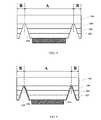
- FIG. 10is a sectional view of a flip chip LED of Embodiment 3 of the present disclosure.
- FIG. 11is a sectional view of a flip chip LED of Embodiment 4 of the present disclosure.
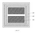
- FIG. 12is a top plan view of the flip chip LED of Embodiment 4 of the present disclosure.
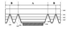
- 100growth substrate; 101 : N-type layer; 102 : light emitting layer; 103 : P-type layer; 104 : metal electrode; 105 : insulating layer; 106 : V-type opening structure; 107 : solder paste; 108 : reflective layer; 109 : W-type opening structure; A: epitaxial bulk layer; B: barrier structure.
- a GaN-based flip-chip LEDcomprises: a growth substrate 100 , an N-type layer 101 , a light emitting layer 102 , a P-type layer 103 , a metal electrode 104 , an insulating layer 105 , a V-type opening structure 106 , an epitaxial bulk layer A and a barrier structure B.
- the above GaN-based flip-chip LED structurecomprises a growth substrate 100 , which is a sapphire substrate; an epitaxial layer, formed on the light emitting layer 102 , wherein, the epitaxial layer comprises an N-type layer 101 , a light emitting layer 102 and a P-type layer 103 in successive; a V-type opening structure 106 , which is on the epitaxial layer edge and extends to the growth substrate 100 surface, making parts of the side wall of the epitaxial layer and the substrate surface exposed, so that the epitaxial layer is divided into an epitaxial bulk layer A and a barrier structure B.
- the barrier structure BAs the barrier structure B is isolated from the epitaxial bulk layer A, it can act as a “barrier wall” to increase soldering tin climbing difficulty as much as possible; in addition, as the chip cutting line is outside the B rather than in the V-type channel, the insulating layer inside the V-type channel is not prone to break due to cutting stress, thus effectively avoiding short circuit caused by overflow of the solder paste 107 in usage of the chip and improving reliability and yield of the flip-chip LED chip; a metal electrode 104 , formed on part of the epitaxial bulk layer A; an insulating layer 105 , formed on the V-type opening structure 106 , as the metal electrode isolating layer.
- FIGS. 5-9are the sectional schematic diagrams of the fabrication process of the flip-chip LED structure, details of which are as follows:
- the growth substrate 100is sapphire, used for forming the epitaxy substrate of the GaN-based flip-chip LED; however, it should be recognized that, the growth substrate 100 can be silicon carbide, gallium nitride, silicon or other substrates.
- the epitaxial layercomprises an N-GaN layer 101 , a light emitting layer 102 and a P-GaN 103 in successive; further, grow a GaN buffer layer on the growth substrate before growth of the epitaxial layer to get better lattice quality.
- V-type opening structure 106from the P-GaN-layer surface 103 of the epitaxial layer downwards, which extends to the growth substrate 100 surface, making parts of the side wall of the epitaxial layer the substrate surface exposed, so that the epitaxial layer is divided into an epitaxial bulk layer A and a barrier structure B, i.e., the barrier structure B is completely isolated from the epitaxial bulk layer A.
- the insulating layer 105is preferably a distributed Bragg reflective layer alternatively stacked by several layers of SiO 2 and TiO 2 ; thin and polish the sapphire growth substrate with grinding equipment, and cut the chip through cutting and splitting, wherein, the epitaxial bulk layer A of each chip at least remains a barrier structure B for insulating protection, which effectively protects the epitaxial layer side wall of the chip and overcomes easy break of the cladding material of the insulating layer in conventional chip during chip cutting, thus avoiding short circuit due to overflow of the solder paste or other solid crystal conductive materials in usage of the chip and improving reliability and yield of the flip-chip LED chip; in addition, as the barrier structure B is completely isolated from the epitaxial bulk layer A, even when the insulating layer cladding material breaks on the barrier structure B during chip cutting, it will not cause short circuit due to overflow of the solder
- the reflective layer 108can be a metal reflective layer, a distributed Bragg reflective layer or an omni-directional reflective layer; in this embodiment, the reflective layer 108 is preferably a metal reflective layer, and the metal reflective layer may comprise Ni, Pt, Ag, Al or Rh.
- the opening structure formed on the epitaxial layeris W-type (a variant of V-type, i.e., the opening structure is not limited to an one-dimensional grating, but can be a combination of two or several V-type barriers, and the barrier shape is not limited to V-type, but can be U-type or other curve shapes) rather than V-type; it should be noted that in the W-type opening structure 109 , the V-type opening that is far from the epitaxial layer edge extends to the substrate 100 surface, while the V-type opening in the W-type opening structure 109 close to the epitaxial layer edge is an concave structure for blocking and may not extend to the substrate 100 surface.
- W-typea variant of V-type, i.e., the opening structure is not limited to an one-dimensional grating, but can be a combination of two or several V-type barriers, and the barrier shape is not limited to V-type, but can be U-type or other curve shapes
Landscapes
- Led Device Packages (AREA)
- Led Devices (AREA)
Abstract
Description
- The present application is a continuation of, and claims priority to, PCT/CN2014/094876 filed on Dec. 25, 2014, which claims priority to Chinese Patent Application No. 201410248717.8 filed on Jun. 6, 2014. The disclosures of these applications are hereby incorporated by reference in their entirety.
- Light-emitting diodes (LEDs), due to long service life and low energy consumption, are applied in various fields. Especially, with great improvement of lighting performance indicators, LED application extends widely to optical display device, traffic sign, data storage device, communication device, lighting device, etc. The III-V-group compound semiconductors, represented by GaN, have huge application potential in optoelectronic device fields like high-brightness blue-light LED, blue-light laser and attract widespread concerns, thanks to wide band gap, high lighting efficiency, high electron saturation drift velocity and stable chemical property.
- However, current semiconductor LEDs may have low light-emitting efficiency. For normal un-packaged LED, a large amount of energy is aggregated inside the device and cannot be emitted, resulting in energy waste and reduction of the LED service life. Therefore, a major concern is to improve the light-emitting efficiency of the semiconductor LEDs. Based on application requirements, many methods to improve LED light-emitting efficiency have been applied in device structures, such transparent substrate, surface roughening, metal reflector structure, flip-chip, etc. Featured with large current, low voltage, high light-emitting efficiency and no-wire bonding, flip chip arises increasing interests.
- At present, the flip-chip LED chip is designed in rectangle shape and layered stack structure composed of a substrate, an epitaxial layer, a P-type ohmic contact layer (also reflective metal layer), an insulating layer and an N-type ohmic contact layer from bottom to up, where the metal layer is a large face structure. Therefore, the design of insulating layer is particularly important. Once the insulating layer is broken, it may cause short-circuit of P and N electrodes; the insulating layer inside the chip is stable and not readily broken. However, the insulating layer at the chip edge is more prone to breaking during chip cutting. In addition, in consideration of light-emitting efficiency and current distribution of chip, in particular for large size chip design, size of P and N metal electrodes, limit position, if solder paste welding is adopted in package, it may cause uneven solder paste coating, overflow out of welding plate area, etc. If the insulating layer at chip edge is damaged, it may cause poor circuit and electric leakage, as shown in
FIGS. 1 and 2 , thus influencing package yield and promotion application of flip-chip. - Various embodiments of the present disclose can overcome at least some of the deficiencies in existing technologies. In an aspect, a flip-chip LED chip with improved reliability and fabrication method is provided, adopting a special barrier structure in chip design and fabrication process to radically solve internal short-circuit of the chip caused by overflow of solder paste or other solid crystal conductive materials.
- In some embodiments, a barrier structure is fabricated at the epitaxial layer edge of the flip-chip LED chip to overcome easy breaking of the cladding material of conventional chip insulating layer during chip cutting. In this way, a new type of insulating protection structure is formed to effectively protect the chip side wall, thus avoiding short-circuit of the chip caused by overflow of solder paste or other solid crystal conductive materials and improving chip reliability.
- According to some embodiments, a flip-chip LED structure comprises: a substrate; an epitaxial layer on the substrate, wherein, the epitaxial layer comprises: a first semiconductor layer, a second semiconductor layer and a light emitting layer between the first semiconductor layer and the second semiconductor layer; at least one opening structure, which is on the epitaxial layer edge and extends to the substrate surface, making parts of the side wall of the epitaxial layer and the substrate surface exposed, so that the epitaxial layer is divided into an epitaxial bulk layer and a barrier structure; and an insulating layer on the opening structure as the metal electrode isolating layer.
- The flip-chip LED structure may also comprise an additional reflective layer on the epitaxial layer before at least one opening structure is formed, wherein, the reflective layer can be a metal reflective layer, a distributed Bragg reflective layer or an omni-directional reflective layer; it may also comprise a metal electrode on the epitaxial layer after the insulating layer is formed.
- In another aspect, a fabrication method of a flip-chip LED is provided, comprising: 1) providing a substrate; 2) fabricating an epitaxial layer on the substrate, wherein, the epitaxial layer comprises: a first semiconductor layer, a second semiconductor layer and a light emitting layer between the first semiconductor layer and the second semiconductor layer; 3) etching at least one opening structure downward from the epitaxial layer surface through etching process, which extends to the substrate surface, making parts of the side wall of the epitaxial layer and the substrate surface exposed, so that the epitaxial layer is divided into an epitaxial bulk layer and a barrier structure; and 4) deposit an insulating layer on the opening structure as the metal electrode isolating layer.
- The aforesaid fabrication method of flip-chip LED may also comprise the process steps of: forming a reflective layer on the epitaxial layer before at least one opening structure is formed, wherein, the reflective layer can be a metal reflective layer, a distributed Bragg reflective layer or an omni-directional reflective layer; also, fabricate a metal electrode on the epitaxial layer after the insulating layer is formed.
- In some embodiments, the opening structure is U-type, V-type, W-type or any of their combinations.
- In some embodiments, the substrate can be a growth substrate, a heat-dissipating substrate, a bonding substrate or any of their combinations.
- In some embodiments, the growth substrate material can be sapphire (Al2O3), silicon carbide (SiC), gallium nitride (GaN) or any of their combinations.
- In some embodiments, the metal reflective layer comprises Ag, Al, Rh or any of their combinations.
- In some embodiments, the insulating layer can be SiO2, SiNx, TiO2or any of their combinations.
- In some embodiments, the metal electrode can be Ni/Au, Cr/Pt/Au, Ti/Al/Ti/Au or any of their combinations.
- In another aspect, a light-emitting system is provided including a plurality of the flip-chip LEDs described above. The light-emitting system can be used in the areas such as lighting, displays, etc.
- Compared with existing technologies, various embodiments of the present disclosure can have one or more of the following advantages: an opening is fabricated at the epitaxial layer edge of the flip-chip LED chip to form a peripheral or local barrier structure for insulating protection, which effectively protects the chip side wall and overcomes easy breaking of the cladding material of conventional chip insulating layer during chip cutting, thus avoiding short-circuit during usage of the chip due to overflow of solder paste or other solid crystal conductive materials and improving reliability and yield of the flip-chip LED chip.
- Other features and advantages of various embodiments of the present disclosure will be described in detail in the following description.
FIG. 1 is a sectional view of an existing flip-chip LED.FIG. 2 is a top view of an existing flip-chip LED.FIG. 3 is a sectional view of the flip chip LED ofEmbodiment 1 of the present disclosure.FIG. 4 is a top plan view of the flip chip LED ofEmbodiment 1 of the present disclosure.FIG. 5 is schematic sectional view of a flip-chip LED according to Embodiment 2 illustrating a first step of a fabrication process.FIG. 6 is schematic sectional view of the flip-chip LED according to Embodiment 2 illustrating a second step of a fabrication process.FIG. 7 is schematic sectional view of the flip-chip LED according to Embodiment 2 illustrating a third step of a fabrication process.FIG. 8 is schematic sectional view of the flip-chip LED according to Embodiment 2 illustrating a fourth step of a fabrication process.FIG. 9 is schematic sectional view of the flip-chip LED according to Embodiment2 illustrating a fifth step of a fabrication process.FIG. 10 is a sectional view of a flip chip LED of Embodiment 3 of the present disclosure.FIG. 11 is a sectional view of a flip chip LED of Embodiment 4 of the present disclosure.FIG. 12 is a top plan view of the flip chip LED of Embodiment 4 of the present disclosure.- In the drawings:
- 100: growth substrate;101: N-type layer;102: light emitting layer;103: P-type layer;104: metal electrode;105: insulating layer;106: V-type opening structure;107: solder paste;108: reflective layer;109: W-type opening structure; A: epitaxial bulk layer; B: barrier structure.
- Various embodiments of the present disclosure will be described in detail with reference to the accompanying drawings and examples, to help understand and practice the disclosed embodiments, regarding how to solve technical problems using technical approaches for achieving the technical effects. It should be understood that the embodiments and their characteristics described in this disclosure may be combined with each other and such technical proposals are deemed to be within the scope of this disclosure without departing from the spirit of this disclosure.
- As shown in
FIGS. 3 and 4 , a GaN-based flip-chip LED, comprises: agrowth substrate 100, an N-type layer 101, alight emitting layer 102, a P-type layer 103, ametal electrode 104, aninsulating layer 105, a V-type opening structure 106, an epitaxial bulk layer A and a barrier structure B. - Specifically, the above GaN-based flip-chip LED structure comprises a
growth substrate 100, which is a sapphire substrate; an epitaxial layer, formed on thelight emitting layer 102, wherein, the epitaxial layer comprises an N-type layer 101, alight emitting layer 102 and a P-type layer 103 in successive; a V-type opening structure 106, which is on the epitaxial layer edge and extends to thegrowth substrate 100 surface, making parts of the side wall of the epitaxial layer and the substrate surface exposed, so that the epitaxial layer is divided into an epitaxial bulk layer A and a barrier structure B. As the barrier structure B is isolated from the epitaxial bulk layer A, it can act as a “barrier wall” to increase soldering tin climbing difficulty as much as possible; in addition, as the chip cutting line is outside the B rather than in the V-type channel, the insulating layer inside the V-type channel is not prone to break due to cutting stress, thus effectively avoiding short circuit caused by overflow of thesolder paste 107 in usage of the chip and improving reliability and yield of the flip-chip LED chip; ametal electrode 104, formed on part of the epitaxial bulk layer A; aninsulating layer 105, formed on the V-type opening structure 106, as the metal electrode isolating layer. FIGS. 5-9 are the sectional schematic diagrams of the fabrication process of the flip-chip LED structure, details of which are as follows:- As shown in
FIG. 5 , at first, provide agrowth substrate 100; in this embodiment, thegrowth substrate 100 is sapphire, used for forming the epitaxy substrate of the GaN-based flip-chip LED; however, it should be recognized that, thegrowth substrate 100 can be silicon carbide, gallium nitride, silicon or other substrates. - As shown in
FIG. 6 , grow an epitaxial layer on thegrowth substrate 100, wherein, the epitaxial layer comprises an N-GaN layer 101, alight emitting layer 102 and a P-GaN 103 in successive; further, grow a GaN buffer layer on the growth substrate before growth of the epitaxial layer to get better lattice quality. - As shown in
FIG. 7 , define the chip size via ICP etching process and etch a - V-
type opening structure 106 from the P-GaN-layer surface 103 of the epitaxial layer downwards, which extends to thegrowth substrate 100 surface, making parts of the side wall of the epitaxial layer the substrate surface exposed, so that the epitaxial layer is divided into an epitaxial bulk layer A and a barrier structure B, i.e., the barrier structure B is completely isolated from the epitaxial bulk layer A. - As shown in
FIG. 8 , fabricate ametal electrode 104 on part of the epitaxial bulk layer A surface, wherein, themetal electrode 104 prefers to be Cr/Pt/Au material. - As shown in
FIG. 9 , deposit an insulatinglayer 105 on the V-type opening structure 106, as the metal electrode isolating layer, wherein, the insulatinglayer 105 is preferably a distributed Bragg reflective layer alternatively stacked by several layers of SiO2and TiO2; thin and polish the sapphire growth substrate with grinding equipment, and cut the chip through cutting and splitting, wherein, the epitaxial bulk layer A of each chip at least remains a barrier structure B for insulating protection, which effectively protects the epitaxial layer side wall of the chip and overcomes easy break of the cladding material of the insulating layer in conventional chip during chip cutting, thus avoiding short circuit due to overflow of the solder paste or other solid crystal conductive materials in usage of the chip and improving reliability and yield of the flip-chip LED chip; in addition, as the barrier structure B is completely isolated from the epitaxial bulk layer A, even when the insulating layer cladding material breaks on the barrier structure B during chip cutting, it will not cause short circuit due to overflow of the solder paste or other solid crystal conductive materials during usage of the chip, thus effectively improving reliability and yield of the flip-chip LED chip. - As shown in
FIG. 10 , different fromEmbodiment 1, in this embodiment, before forming a V-type opening structure 106 on the epitaxial layer, form areflective layer 108 at first, wherein, thereflective layer 108 can be a metal reflective layer, a distributed Bragg reflective layer or an omni-directional reflective layer; in this embodiment, thereflective layer 108 is preferably a metal reflective layer, and the metal reflective layer may comprise Ni, Pt, Ag, Al or Rh. - As shown in
FIGS. 11 and 12 , different from Embodiment 3, in this embodiment, the opening structure formed on the epitaxial layer is W-type (a variant of V-type, i.e., the opening structure is not limited to an one-dimensional grating, but can be a combination of two or several V-type barriers, and the barrier shape is not limited to V-type, but can be U-type or other curve shapes) rather than V-type; it should be noted that in the W-type opening structure 109, the V-type opening that is far from the epitaxial layer edge extends to thesubstrate 100 surface, while the V-type opening in the W-type opening structure 109 close to the epitaxial layer edge is an concave structure for blocking and may not extend to thesubstrate 100 surface. - Although specific embodiments have been described above in detail, the description is merely for purposes of illustration. It should be appreciated, therefore, that many aspects described above are not intended as required or essential elements unless explicitly stated otherwise. Various modifications of, and equivalent acts corresponding to, the disclosed aspects of the exemplary embodiments, in addition to those described above, can be made by a person of ordinary skill in the art, having the benefit of the present disclosure, without departing from the spirit and scope of the disclosure defined in the following claims, the scope of which is to be accorded the broadest interpretation so as to encompass such modifications and equivalent structures.
Claims (17)
Priority Applications (1)
| Application Number | Priority Date | Filing Date | Title |
|---|---|---|---|
| US17/445,691US11888094B2 (en) | 2014-06-06 | 2021-08-23 | Flip-chip LED structure and fabrication method |
Applications Claiming Priority (3)
| Application Number | Priority Date | Filing Date | Title |
|---|---|---|---|
| CN201410248717.8ACN103996773B (en) | 2014-06-06 | 2014-06-06 | A kind of inverted light-emitting diode (LED) structure and preparation method thereof |
| CN201410248717.8 | 2014-06-06 | ||
| PCT/CN2014/094876WO2015184774A1 (en) | 2014-06-06 | 2014-12-25 | Flip light-emitting diode structure and method for manufacturing same |
Related Parent Applications (1)
| Application Number | Title | Priority Date | Filing Date |
|---|---|---|---|
| PCT/CN2014/094876ContinuationWO2015184774A1 (en) | 2014-06-06 | 2014-12-25 | Flip light-emitting diode structure and method for manufacturing same |
Related Child Applications (1)
| Application Number | Title | Priority Date | Filing Date |
|---|---|---|---|
| US17/445,691ContinuationUS11888094B2 (en) | 2014-06-06 | 2021-08-23 | Flip-chip LED structure and fabrication method |
Publications (2)
| Publication Number | Publication Date |
|---|---|
| US20160365488A1true US20160365488A1 (en) | 2016-12-15 |
| US11127886B2 US11127886B2 (en) | 2021-09-21 |
Family
ID=51310872
Family Applications (2)
| Application Number | Title | Priority Date | Filing Date |
|---|---|---|---|
| US15/236,434Active2035-04-01US11127886B2 (en) | 2014-06-06 | 2016-08-13 | Flip-chip LED with barrier structure |
| US17/445,691Active2035-02-22US11888094B2 (en) | 2014-06-06 | 2021-08-23 | Flip-chip LED structure and fabrication method |
Family Applications After (1)
| Application Number | Title | Priority Date | Filing Date |
|---|---|---|---|
| US17/445,691Active2035-02-22US11888094B2 (en) | 2014-06-06 | 2021-08-23 | Flip-chip LED structure and fabrication method |
Country Status (3)
| Country | Link |
|---|---|
| US (2) | US11127886B2 (en) |
| CN (1) | CN103996773B (en) |
| WO (1) | WO2015184774A1 (en) |
Cited By (1)
| Publication number | Priority date | Publication date | Assignee | Title |
|---|---|---|---|---|
| WO2024245198A1 (en)* | 2023-05-31 | 2024-12-05 | 京东方科技集团股份有限公司 | Light-emitting chip, display device, and manufacturing method |
Families Citing this family (9)
| Publication number | Priority date | Publication date | Assignee | Title |
|---|---|---|---|---|
| CN103996773B (en)* | 2014-06-06 | 2016-09-28 | 厦门市三安光电科技有限公司 | A kind of inverted light-emitting diode (LED) structure and preparation method thereof |
| JP2016174015A (en)* | 2015-03-16 | 2016-09-29 | 株式会社東芝 | Semiconductor light emitting device |
| JP2016174018A (en)* | 2015-03-16 | 2016-09-29 | 株式会社東芝 | Semiconductor light emitting element |
| CN106093710B (en)* | 2016-08-19 | 2018-12-18 | 江西师范大学 | A kind of spool intelligent monitoring and controlling device based on technology of Internet of things |
| CN107845721A (en)* | 2017-10-23 | 2018-03-27 | 山东晶泰星光电科技有限公司 | A kind of LED support for being used for upside-down mounting or vertical LED chip |
| JP7237536B2 (en)* | 2018-11-12 | 2023-03-13 | 株式会社ジャパンディスプレイ | Display device |
| CN113659048B (en)* | 2021-07-22 | 2023-10-20 | 厦门三安光电有限公司 | Flip-chip light emitting diode and preparation method thereof |
| CN113594326B (en)* | 2021-07-29 | 2022-12-20 | 厦门三安光电有限公司 | Light emitting diode, light emitting module and display device |
| CN113644169B (en)* | 2021-08-13 | 2023-07-28 | 福建兆元光电有限公司 | Red light LED chip and manufacturing method thereof |
Citations (4)
| Publication number | Priority date | Publication date | Assignee | Title |
|---|---|---|---|---|
| US20050189558A1 (en)* | 2004-03-01 | 2005-09-01 | Wen-Huang Liu | Flip-chip light-emitting device with micro-reflector |
| US20050281303A1 (en)* | 2004-06-18 | 2005-12-22 | Naochika Horio | Semiconductor light emitting device and manufacturing method thereof |
| US20120267662A1 (en)* | 2009-07-31 | 2012-10-25 | Osram Opto Semiconductors Gmbh | Light-emitting diode chip |
| US20150243706A1 (en)* | 2014-02-27 | 2015-08-27 | Seoul Viosys Co., Ltd. | Light emitting diode and method of fabricating the same |
Family Cites Families (14)
| Publication number | Priority date | Publication date | Assignee | Title |
|---|---|---|---|---|
| JP2003051610A (en)* | 2001-08-03 | 2003-02-21 | Nichia Chem Ind Ltd | LED element |
| JP4201609B2 (en)* | 2003-01-24 | 2008-12-24 | 三洋電機株式会社 | Semiconductor light emitting device and semiconductor device |
| CN1943050B (en)* | 2004-04-20 | 2012-02-22 | 昭和电工株式会社 | Compound semiconductor light-emitting device, wafer thereof, and method for manufacturing the wafer |
| US7723718B1 (en)* | 2005-10-11 | 2010-05-25 | SemiLEDs Optoelectronics Co., Ltd. | Epitaxial structure for metal devices |
| TWI318013B (en)* | 2006-09-05 | 2009-12-01 | Epistar Corp | A light emitting device and the manufacture method thereof |
| DE102009018603B9 (en)* | 2008-04-25 | 2021-01-14 | Samsung Electronics Co., Ltd. | Lighting device and manufacturing method thereof |
| WO2011126248A2 (en)* | 2010-04-06 | 2011-10-13 | Seoul Opto Device Co., Ltd. | Light emitting diode and method of fabricating the same |
| CN102544251B (en)* | 2010-12-27 | 2014-05-07 | 同方光电科技有限公司 | Manufacturing method of large-power vertical light-emitting diode |
| CN102339913B (en)* | 2011-09-30 | 2013-06-19 | 映瑞光电科技(上海)有限公司 | High-voltage LED (Light Emitting Diode) device and manufacturing method thereof |
| CN103531686A (en)* | 2012-07-02 | 2014-01-22 | 东莞市正光光电科技有限公司 | Light emitting element and manufacturing method thereof |
| CN103022334B (en)* | 2012-12-21 | 2016-01-13 | 映瑞光电科技(上海)有限公司 | A kind of high pressure flip LED chips and manufacture method thereof |
| CN203521451U (en)* | 2013-09-05 | 2014-04-02 | 深圳市智讯达光电科技有限公司 | Welding protection structure of flip-chip LED chip and flip-chip LED chip |
| CN103996773B (en)* | 2014-06-06 | 2016-09-28 | 厦门市三安光电科技有限公司 | A kind of inverted light-emitting diode (LED) structure and preparation method thereof |
| TWI583020B (en)* | 2015-07-06 | 2017-05-11 | 隆達電子股份有限公司 | Light-emitting element and light-emitting device |
- 2014
- 2014-06-06CNCN201410248717.8Apatent/CN103996773B/enactiveActive
- 2014-12-25WOPCT/CN2014/094876patent/WO2015184774A1/enactiveApplication Filing
- 2016
- 2016-08-13USUS15/236,434patent/US11127886B2/enactiveActive
- 2021
- 2021-08-23USUS17/445,691patent/US11888094B2/enactiveActive
Patent Citations (4)
| Publication number | Priority date | Publication date | Assignee | Title |
|---|---|---|---|---|
| US20050189558A1 (en)* | 2004-03-01 | 2005-09-01 | Wen-Huang Liu | Flip-chip light-emitting device with micro-reflector |
| US20050281303A1 (en)* | 2004-06-18 | 2005-12-22 | Naochika Horio | Semiconductor light emitting device and manufacturing method thereof |
| US20120267662A1 (en)* | 2009-07-31 | 2012-10-25 | Osram Opto Semiconductors Gmbh | Light-emitting diode chip |
| US20150243706A1 (en)* | 2014-02-27 | 2015-08-27 | Seoul Viosys Co., Ltd. | Light emitting diode and method of fabricating the same |
Cited By (1)
| Publication number | Priority date | Publication date | Assignee | Title |
|---|---|---|---|---|
| WO2024245198A1 (en)* | 2023-05-31 | 2024-12-05 | 京东方科技集团股份有限公司 | Light-emitting chip, display device, and manufacturing method |
Also Published As
| Publication number | Publication date |
|---|---|
| CN103996773A (en) | 2014-08-20 |
| US20210384383A1 (en) | 2021-12-09 |
| US11888094B2 (en) | 2024-01-30 |
| CN103996773B (en) | 2016-09-28 |
| WO2015184774A1 (en) | 2015-12-10 |
| US11127886B2 (en) | 2021-09-21 |
Similar Documents
| Publication | Publication Date | Title |
|---|---|---|
| US11888094B2 (en) | Flip-chip LED structure and fabrication method | |
| TWI720053B (en) | Light-emitting element and manufacturing method thereof | |
| US10403796B2 (en) | Light emitting device and method of fabricating the same | |
| US9391239B2 (en) | Light emitting diode | |
| KR101081135B1 (en) | Light emitting device, method for fabricating the light emitting device and light emitting device package | |
| KR101658838B1 (en) | Light emitting device and method for fabricating the same | |
| US10205057B2 (en) | Flip-chip light emitting diode and fabrication method | |
| EP2408025A1 (en) | Light emitting diode and manufacturing method thereof | |
| KR20110128545A (en) | Light emitting device, manufacturing method and light emitting device package | |
| US20120074384A1 (en) | Protection for the epitaxial structure of metal devices | |
| KR100649769B1 (en) | Semiconductor Light Emitting Diode and Manufacturing Method Thereof | |
| KR20110094810A (en) | Light emitting device, light emitting device manufacturing method and light emitting device package | |
| KR20110126793A (en) | Light emitting device, manufacturing method and light emitting device package | |
| EP2626916A1 (en) | Light emitting diode and manufacturing method thereof | |
| KR101091048B1 (en) | Semiconductor light emitting device | |
| KR101158077B1 (en) | High efficiency light emitting diode and method of fabricating the same | |
| US20140151630A1 (en) | Protection for the epitaxial structure of metal devices | |
| KR102217128B1 (en) | Light emitting diode and method of fabricating the same | |
| KR101138978B1 (en) | High efficiency light emitting diode and method of fabricating the same | |
| KR101340322B1 (en) | Lateral power LED | |
| US8728834B2 (en) | Semiconductor device and a method of manufacturing the same | |
| KR100785451B1 (en) | A light emitting device having a patterned transparent electrode layer and a method of manufacturing the same | |
| CN117393677A (en) | Light-emitting diode device and wafer structure | |
| KR20110101464A (en) | Light emitting device, light emitting device package and manufacturing method | |
| TW202131529A (en) | Light-emitting element and manufacturing method thereof |
Legal Events
| Date | Code | Title | Description |
|---|---|---|---|
| AS | Assignment | Owner name:XIAMEN SANAN OPTOELECTRONICS TECHNOLOGY CO., LTD., CHINA Free format text:ASSIGNMENT OF ASSIGNORS INTEREST;ASSIGNORS:HE, ANHE;LIN, SU-HUI;ZHENG, JIANSEN;AND OTHERS;SIGNING DATES FROM 20160624 TO 20160628;REEL/FRAME:039427/0257 Owner name:XIAMEN SANAN OPTOELECTRONICS TECHNOLOGY CO., LTD., Free format text:ASSIGNMENT OF ASSIGNORS INTEREST;ASSIGNORS:HE, ANHE;LIN, SU-HUI;ZHENG, JIANSEN;AND OTHERS;SIGNING DATES FROM 20160624 TO 20160628;REEL/FRAME:039427/0257 | |
| STPP | Information on status: patent application and granting procedure in general | Free format text:NON FINAL ACTION MAILED | |
| STPP | Information on status: patent application and granting procedure in general | Free format text:RESPONSE TO NON-FINAL OFFICE ACTION ENTERED AND FORWARDED TO EXAMINER | |
| STPP | Information on status: patent application and granting procedure in general | Free format text:FINAL REJECTION MAILED | |
| STPP | Information on status: patent application and granting procedure in general | Free format text:ADVISORY ACTION MAILED | |
| STPP | Information on status: patent application and granting procedure in general | Free format text:DOCKETED NEW CASE - READY FOR EXAMINATION | |
| STPP | Information on status: patent application and granting procedure in general | Free format text:NON FINAL ACTION MAILED | |
| STPP | Information on status: patent application and granting procedure in general | Free format text:FINAL REJECTION MAILED | |
| STPP | Information on status: patent application and granting procedure in general | Free format text:ADVISORY ACTION MAILED | |
| STPP | Information on status: patent application and granting procedure in general | Free format text:NON FINAL ACTION MAILED | |
| STPP | Information on status: patent application and granting procedure in general | Free format text:FINAL REJECTION MAILED | |
| STPP | Information on status: patent application and granting procedure in general | Free format text:RESPONSE AFTER FINAL ACTION FORWARDED TO EXAMINER | |
| STPP | Information on status: patent application and granting procedure in general | Free format text:EX PARTE QUAYLE ACTION MAILED | |
| STPP | Information on status: patent application and granting procedure in general | Free format text:RESPONSE TO EX PARTE QUAYLE ACTION ENTERED AND FORWARDED TO EXAMINER | |
| STPP | Information on status: patent application and granting procedure in general | Free format text:NOTICE OF ALLOWANCE MAILED -- APPLICATION RECEIVED IN OFFICE OF PUBLICATIONS | |
| STPP | Information on status: patent application and granting procedure in general | Free format text:PUBLICATIONS -- ISSUE FEE PAYMENT RECEIVED | |
| STCF | Information on status: patent grant | Free format text:PATENTED CASE | |
| AS | Assignment | Owner name:QUANZHOU SANAN SEMICONDUCTOR TECHNOLOGY CO., LTD., CHINA Free format text:ASSIGNMENT OF ASSIGNORS INTEREST;ASSIGNOR:XIAMEN SANAN OPTOELECTRONICS TECHNOLOGY CO., LTD.;REEL/FRAME:065302/0223 Effective date:20230919 | |
| MAFP | Maintenance fee payment | Free format text:PAYMENT OF MAINTENANCE FEE, 4TH YEAR, LARGE ENTITY (ORIGINAL EVENT CODE: M1551); ENTITY STATUS OF PATENT OWNER: LARGE ENTITY Year of fee payment:4 |