US20160336302A1 - Discontinuous patterned bonds for semiconductor devices and associated systems and methods - Google Patents
Discontinuous patterned bonds for semiconductor devices and associated systems and methodsDownload PDFInfo
- Publication number
- US20160336302A1 US20160336302A1US15/159,237US201615159237AUS2016336302A1US 20160336302 A1US20160336302 A1US 20160336302A1US 201615159237 AUS201615159237 AUS 201615159237AUS 2016336302 A1US2016336302 A1US 2016336302A1
- Authority
- US
- United States
- Prior art keywords
- substrate
- semiconductor device
- solid
- bond metal
- state transducer
- Prior art date
- Legal status (The legal status is an assumption and is not a legal conclusion. Google has not performed a legal analysis and makes no representation as to the accuracy of the status listed.)
- Granted
Links
Images


Classifications
- H—ELECTRICITY
- H01—ELECTRIC ELEMENTS
- H01L—SEMICONDUCTOR DEVICES NOT COVERED BY CLASS H10
- H01L25/00—Assemblies consisting of a plurality of semiconductor or other solid state devices
- H01L25/03—Assemblies consisting of a plurality of semiconductor or other solid state devices all the devices being of a type provided for in a single subclass of subclasses H10B, H10D, H10F, H10H, H10K or H10N, e.g. assemblies of rectifier diodes
- H01L25/04—Assemblies consisting of a plurality of semiconductor or other solid state devices all the devices being of a type provided for in a single subclass of subclasses H10B, H10D, H10F, H10H, H10K or H10N, e.g. assemblies of rectifier diodes the devices not having separate containers
- H01L25/075—Assemblies consisting of a plurality of semiconductor or other solid state devices all the devices being of a type provided for in a single subclass of subclasses H10B, H10D, H10F, H10H, H10K or H10N, e.g. assemblies of rectifier diodes the devices not having separate containers the devices being of a type provided for in group H10H20/00
- H01L25/0753—Assemblies consisting of a plurality of semiconductor or other solid state devices all the devices being of a type provided for in a single subclass of subclasses H10B, H10D, H10F, H10H, H10K or H10N, e.g. assemblies of rectifier diodes the devices not having separate containers the devices being of a type provided for in group H10H20/00 the devices being arranged next to each other
- H—ELECTRICITY
- H10—SEMICONDUCTOR DEVICES; ELECTRIC SOLID-STATE DEVICES NOT OTHERWISE PROVIDED FOR
- H10H—INORGANIC LIGHT-EMITTING SEMICONDUCTOR DEVICES HAVING POTENTIAL BARRIERS
- H10H20/00—Individual inorganic light-emitting semiconductor devices having potential barriers, e.g. light-emitting diodes [LED]
- H10H20/80—Constructional details
- H10H20/85—Packages
- H10H20/857—Interconnections, e.g. lead-frames, bond wires or solder balls
- H—ELECTRICITY
- H01—ELECTRIC ELEMENTS
- H01L—SEMICONDUCTOR DEVICES NOT COVERED BY CLASS H10
- H01L21/00—Processes or apparatus adapted for the manufacture or treatment of semiconductor or solid state devices or of parts thereof
- H01L21/02—Manufacture or treatment of semiconductor devices or of parts thereof
- H01L21/027—Making masks on semiconductor bodies for further photolithographic processing not provided for in group H01L21/18 or H01L21/34
- H—ELECTRICITY
- H01—ELECTRIC ELEMENTS
- H01L—SEMICONDUCTOR DEVICES NOT COVERED BY CLASS H10
- H01L21/00—Processes or apparatus adapted for the manufacture or treatment of semiconductor or solid state devices or of parts thereof
- H01L21/02—Manufacture or treatment of semiconductor devices or of parts thereof
- H01L21/04—Manufacture or treatment of semiconductor devices or of parts thereof the devices having potential barriers, e.g. a PN junction, depletion layer or carrier concentration layer
- H01L21/18—Manufacture or treatment of semiconductor devices or of parts thereof the devices having potential barriers, e.g. a PN junction, depletion layer or carrier concentration layer the devices having semiconductor bodies comprising elements of Group IV of the Periodic Table or AIIIBV compounds with or without impurities, e.g. doping materials
- H01L21/185—Joining of semiconductor bodies for junction formation
- H01L21/187—Joining of semiconductor bodies for junction formation by direct bonding
- H—ELECTRICITY
- H01—ELECTRIC ELEMENTS
- H01L—SEMICONDUCTOR DEVICES NOT COVERED BY CLASS H10
- H01L21/00—Processes or apparatus adapted for the manufacture or treatment of semiconductor or solid state devices or of parts thereof
- H01L21/02—Manufacture or treatment of semiconductor devices or of parts thereof
- H01L21/04—Manufacture or treatment of semiconductor devices or of parts thereof the devices having potential barriers, e.g. a PN junction, depletion layer or carrier concentration layer
- H01L21/18—Manufacture or treatment of semiconductor devices or of parts thereof the devices having potential barriers, e.g. a PN junction, depletion layer or carrier concentration layer the devices having semiconductor bodies comprising elements of Group IV of the Periodic Table or AIIIBV compounds with or without impurities, e.g. doping materials
- H01L21/20—Deposition of semiconductor materials on a substrate, e.g. epitaxial growth solid phase epitaxy
- H01L21/2003—Deposition of semiconductor materials on a substrate, e.g. epitaxial growth solid phase epitaxy characterised by the substrate
- H01L21/2007—Bonding of semiconductor wafers to insulating substrates or to semiconducting substrates using an intermediate insulating layer
- H—ELECTRICITY
- H01—ELECTRIC ELEMENTS
- H01L—SEMICONDUCTOR DEVICES NOT COVERED BY CLASS H10
- H01L21/00—Processes or apparatus adapted for the manufacture or treatment of semiconductor or solid state devices or of parts thereof
- H01L21/02—Manufacture or treatment of semiconductor devices or of parts thereof
- H01L21/04—Manufacture or treatment of semiconductor devices or of parts thereof the devices having potential barriers, e.g. a PN junction, depletion layer or carrier concentration layer
- H01L21/34—Manufacture or treatment of semiconductor devices or of parts thereof the devices having potential barriers, e.g. a PN junction, depletion layer or carrier concentration layer the devices having semiconductor bodies not provided for in groups H01L21/18, H10D48/04 and H10D48/07, with or without impurities, e.g. doping materials
- H01L21/44—Manufacture of electrodes on semiconductor bodies using processes or apparatus not provided for in groups H01L21/38 - H01L21/428
- H01L21/447—Manufacture of electrodes on semiconductor bodies using processes or apparatus not provided for in groups H01L21/38 - H01L21/428 involving the application of pressure, e.g. thermo-compression bonding
- H—ELECTRICITY
- H01—ELECTRIC ELEMENTS
- H01L—SEMICONDUCTOR DEVICES NOT COVERED BY CLASS H10
- H01L23/00—Details of semiconductor or other solid state devices
- H01L23/48—Arrangements for conducting electric current to or from the solid state body in operation, e.g. leads, terminal arrangements ; Selection of materials therefor
- H01L23/488—Arrangements for conducting electric current to or from the solid state body in operation, e.g. leads, terminal arrangements ; Selection of materials therefor consisting of soldered or bonded constructions
- H01L23/495—Lead-frames or other flat leads
- H01L23/49503—Lead-frames or other flat leads characterised by the die pad
- H01L23/49513—Lead-frames or other flat leads characterised by the die pad having bonding material between chip and die pad
- H—ELECTRICITY
- H01—ELECTRIC ELEMENTS
- H01L—SEMICONDUCTOR DEVICES NOT COVERED BY CLASS H10
- H01L24/00—Arrangements for connecting or disconnecting semiconductor or solid-state bodies; Methods or apparatus related thereto
- H01L24/01—Means for bonding being attached to, or being formed on, the surface to be connected, e.g. chip-to-package, die-attach, "first-level" interconnects; Manufacturing methods related thereto
- H01L24/02—Bonding areas ; Manufacturing methods related thereto
- H01L24/04—Structure, shape, material or disposition of the bonding areas prior to the connecting process
- H01L24/06—Structure, shape, material or disposition of the bonding areas prior to the connecting process of a plurality of bonding areas
- H—ELECTRICITY
- H01—ELECTRIC ELEMENTS
- H01L—SEMICONDUCTOR DEVICES NOT COVERED BY CLASS H10
- H01L24/00—Arrangements for connecting or disconnecting semiconductor or solid-state bodies; Methods or apparatus related thereto
- H01L24/80—Methods for connecting semiconductor or other solid state bodies using means for bonding being attached to, or being formed on, the surface to be connected
- H01L24/83—Methods for connecting semiconductor or other solid state bodies using means for bonding being attached to, or being formed on, the surface to be connected using a layer connector
- H—ELECTRICITY
- H01—ELECTRIC ELEMENTS
- H01L—SEMICONDUCTOR DEVICES NOT COVERED BY CLASS H10
- H01L24/00—Arrangements for connecting or disconnecting semiconductor or solid-state bodies; Methods or apparatus related thereto
- H01L24/93—Batch processes
- H01L24/94—Batch processes at wafer-level, i.e. with connecting carried out on a wafer comprising a plurality of undiced individual devices
- H—ELECTRICITY
- H01—ELECTRIC ELEMENTS
- H01L—SEMICONDUCTOR DEVICES NOT COVERED BY CLASS H10
- H01L24/00—Arrangements for connecting or disconnecting semiconductor or solid-state bodies; Methods or apparatus related thereto
- H01L24/93—Batch processes
- H01L24/95—Batch processes at chip-level, i.e. with connecting carried out on a plurality of singulated devices, i.e. on diced chips
- H01L24/97—Batch processes at chip-level, i.e. with connecting carried out on a plurality of singulated devices, i.e. on diced chips the devices being connected to a common substrate, e.g. interposer, said common substrate being separable into individual assemblies after connecting
- H01L33/0079—
- H01L33/0095—
- H01L33/486—
- H01L33/62—
- H—ELECTRICITY
- H10—SEMICONDUCTOR DEVICES; ELECTRIC SOLID-STATE DEVICES NOT OTHERWISE PROVIDED FOR
- H10F—INORGANIC SEMICONDUCTOR DEVICES SENSITIVE TO INFRARED RADIATION, LIGHT, ELECTROMAGNETIC RADIATION OF SHORTER WAVELENGTH OR CORPUSCULAR RADIATION
- H10F71/00—Manufacture or treatment of devices covered by this subclass
- H—ELECTRICITY
- H10—SEMICONDUCTOR DEVICES; ELECTRIC SOLID-STATE DEVICES NOT OTHERWISE PROVIDED FOR
- H10H—INORGANIC LIGHT-EMITTING SEMICONDUCTOR DEVICES HAVING POTENTIAL BARRIERS
- H10H20/00—Individual inorganic light-emitting semiconductor devices having potential barriers, e.g. light-emitting diodes [LED]
- H10H20/01—Manufacture or treatment
- H10H20/011—Manufacture or treatment of bodies, e.g. forming semiconductor layers
- H10H20/013—Manufacture or treatment of bodies, e.g. forming semiconductor layers having light-emitting regions comprising only Group III-V materials
- H10H20/0133—Manufacture or treatment of bodies, e.g. forming semiconductor layers having light-emitting regions comprising only Group III-V materials with a substrate not being Group III-V materials
- H—ELECTRICITY
- H10—SEMICONDUCTOR DEVICES; ELECTRIC SOLID-STATE DEVICES NOT OTHERWISE PROVIDED FOR
- H10H—INORGANIC LIGHT-EMITTING SEMICONDUCTOR DEVICES HAVING POTENTIAL BARRIERS
- H10H20/00—Individual inorganic light-emitting semiconductor devices having potential barriers, e.g. light-emitting diodes [LED]
- H10H20/01—Manufacture or treatment
- H10H20/011—Manufacture or treatment of bodies, e.g. forming semiconductor layers
- H10H20/018—Bonding of wafers
- H—ELECTRICITY
- H10—SEMICONDUCTOR DEVICES; ELECTRIC SOLID-STATE DEVICES NOT OTHERWISE PROVIDED FOR
- H10H—INORGANIC LIGHT-EMITTING SEMICONDUCTOR DEVICES HAVING POTENTIAL BARRIERS
- H10H20/00—Individual inorganic light-emitting semiconductor devices having potential barriers, e.g. light-emitting diodes [LED]
- H10H20/80—Constructional details
- H10H20/85—Packages
- H10H20/8506—Containers
- H—ELECTRICITY
- H01—ELECTRIC ELEMENTS
- H01L—SEMICONDUCTOR DEVICES NOT COVERED BY CLASS H10
- H01L2224/00—Indexing scheme for arrangements for connecting or disconnecting semiconductor or solid-state bodies and methods related thereto as covered by H01L24/00
- H01L2224/01—Means for bonding being attached to, or being formed on, the surface to be connected, e.g. chip-to-package, die-attach, "first-level" interconnects; Manufacturing methods related thereto
- H01L2224/26—Layer connectors, e.g. plate connectors, solder or adhesive layers; Manufacturing methods related thereto
- H01L2224/31—Structure, shape, material or disposition of the layer connectors after the connecting process
- H01L2224/32—Structure, shape, material or disposition of the layer connectors after the connecting process of an individual layer connector
- H01L2224/321—Disposition
- H01L2224/32151—Disposition the layer connector connecting between a semiconductor or solid-state body and an item not being a semiconductor or solid-state body, e.g. chip-to-substrate, chip-to-passive
- H01L2224/32221—Disposition the layer connector connecting between a semiconductor or solid-state body and an item not being a semiconductor or solid-state body, e.g. chip-to-substrate, chip-to-passive the body and the item being stacked
- H01L2224/32225—Disposition the layer connector connecting between a semiconductor or solid-state body and an item not being a semiconductor or solid-state body, e.g. chip-to-substrate, chip-to-passive the body and the item being stacked the item being non-metallic, e.g. insulating substrate with or without metallisation
- H—ELECTRICITY
- H01—ELECTRIC ELEMENTS
- H01L—SEMICONDUCTOR DEVICES NOT COVERED BY CLASS H10
- H01L2224/00—Indexing scheme for arrangements for connecting or disconnecting semiconductor or solid-state bodies and methods related thereto as covered by H01L24/00
- H01L2224/01—Means for bonding being attached to, or being formed on, the surface to be connected, e.g. chip-to-package, die-attach, "first-level" interconnects; Manufacturing methods related thereto
- H01L2224/26—Layer connectors, e.g. plate connectors, solder or adhesive layers; Manufacturing methods related thereto
- H01L2224/31—Structure, shape, material or disposition of the layer connectors after the connecting process
- H01L2224/32—Structure, shape, material or disposition of the layer connectors after the connecting process of an individual layer connector
- H01L2224/321—Disposition
- H01L2224/32151—Disposition the layer connector connecting between a semiconductor or solid-state body and an item not being a semiconductor or solid-state body, e.g. chip-to-substrate, chip-to-passive
- H01L2224/32221—Disposition the layer connector connecting between a semiconductor or solid-state body and an item not being a semiconductor or solid-state body, e.g. chip-to-substrate, chip-to-passive the body and the item being stacked
- H01L2224/32245—Disposition the layer connector connecting between a semiconductor or solid-state body and an item not being a semiconductor or solid-state body, e.g. chip-to-substrate, chip-to-passive the body and the item being stacked the item being metallic
- H—ELECTRICITY
- H01—ELECTRIC ELEMENTS
- H01L—SEMICONDUCTOR DEVICES NOT COVERED BY CLASS H10
- H01L2224/00—Indexing scheme for arrangements for connecting or disconnecting semiconductor or solid-state bodies and methods related thereto as covered by H01L24/00
- H01L2224/80—Methods for connecting semiconductor or other solid state bodies using means for bonding being attached to, or being formed on, the surface to be connected
- H01L2224/83—Methods for connecting semiconductor or other solid state bodies using means for bonding being attached to, or being formed on, the surface to be connected using a layer connector
- H01L2224/83001—Methods for connecting semiconductor or other solid state bodies using means for bonding being attached to, or being formed on, the surface to be connected using a layer connector involving a temporary auxiliary member not forming part of the bonding apparatus
- H01L2224/83005—Methods for connecting semiconductor or other solid state bodies using means for bonding being attached to, or being formed on, the surface to be connected using a layer connector involving a temporary auxiliary member not forming part of the bonding apparatus being a temporary or sacrificial substrate
- H—ELECTRICITY
- H01—ELECTRIC ELEMENTS
- H01L—SEMICONDUCTOR DEVICES NOT COVERED BY CLASS H10
- H01L2224/00—Indexing scheme for arrangements for connecting or disconnecting semiconductor or solid-state bodies and methods related thereto as covered by H01L24/00
- H01L2224/80—Methods for connecting semiconductor or other solid state bodies using means for bonding being attached to, or being formed on, the surface to be connected
- H01L2224/83—Methods for connecting semiconductor or other solid state bodies using means for bonding being attached to, or being formed on, the surface to be connected using a layer connector
- H01L2224/8312—Aligning
- H01L2224/83121—Active alignment, i.e. by apparatus steering, e.g. optical alignment using marks or sensors
- H—ELECTRICITY
- H01—ELECTRIC ELEMENTS
- H01L—SEMICONDUCTOR DEVICES NOT COVERED BY CLASS H10
- H01L2224/00—Indexing scheme for arrangements for connecting or disconnecting semiconductor or solid-state bodies and methods related thereto as covered by H01L24/00
- H01L2224/80—Methods for connecting semiconductor or other solid state bodies using means for bonding being attached to, or being formed on, the surface to be connected
- H01L2224/83—Methods for connecting semiconductor or other solid state bodies using means for bonding being attached to, or being formed on, the surface to be connected using a layer connector
- H01L2224/8312—Aligning
- H01L2224/83136—Aligning involving guiding structures, e.g. spacers or supporting members
- H01L2224/83138—Aligning involving guiding structures, e.g. spacers or supporting members the guiding structures being at least partially left in the finished device
- H01L2224/8314—Guiding structures outside the body
- H—ELECTRICITY
- H01—ELECTRIC ELEMENTS
- H01L—SEMICONDUCTOR DEVICES NOT COVERED BY CLASS H10
- H01L2224/00—Indexing scheme for arrangements for connecting or disconnecting semiconductor or solid-state bodies and methods related thereto as covered by H01L24/00
- H01L2224/80—Methods for connecting semiconductor or other solid state bodies using means for bonding being attached to, or being formed on, the surface to be connected
- H01L2224/83—Methods for connecting semiconductor or other solid state bodies using means for bonding being attached to, or being formed on, the surface to be connected using a layer connector
- H01L2224/8319—Arrangement of the layer connectors prior to mounting
- H01L2224/83193—Arrangement of the layer connectors prior to mounting wherein the layer connectors are disposed on both the semiconductor or solid-state body and another item or body to be connected to the semiconductor or solid-state body
- H—ELECTRICITY
- H01—ELECTRIC ELEMENTS
- H01L—SEMICONDUCTOR DEVICES NOT COVERED BY CLASS H10
- H01L24/00—Arrangements for connecting or disconnecting semiconductor or solid-state bodies; Methods or apparatus related thereto
- H01L24/01—Means for bonding being attached to, or being formed on, the surface to be connected, e.g. chip-to-package, die-attach, "first-level" interconnects; Manufacturing methods related thereto
- H01L24/26—Layer connectors, e.g. plate connectors, solder or adhesive layers; Manufacturing methods related thereto
- H01L24/31—Structure, shape, material or disposition of the layer connectors after the connecting process
- H01L24/32—Structure, shape, material or disposition of the layer connectors after the connecting process of an individual layer connector
- H—ELECTRICITY
- H01—ELECTRIC ELEMENTS
- H01L—SEMICONDUCTOR DEVICES NOT COVERED BY CLASS H10
- H01L2924/00—Indexing scheme for arrangements or methods for connecting or disconnecting semiconductor or solid-state bodies as covered by H01L24/00
- H01L2924/10—Details of semiconductor or other solid state devices to be connected
- H01L2924/11—Device type
- H01L2924/12—Passive devices, e.g. 2 terminal devices
- H01L2924/1204—Optical Diode
- H01L2924/12041—LED
- H—ELECTRICITY
- H01—ELECTRIC ELEMENTS
- H01L—SEMICONDUCTOR DEVICES NOT COVERED BY CLASS H10
- H01L2924/00—Indexing scheme for arrangements or methods for connecting or disconnecting semiconductor or solid-state bodies as covered by H01L24/00
- H01L2924/10—Details of semiconductor or other solid state devices to be connected
- H01L2924/11—Device type
- H01L2924/12—Passive devices, e.g. 2 terminal devices
- H01L2924/1204—Optical Diode
- H01L2924/12042—LASER
Definitions
- the present technologyis directed generally to discontinuous bonds for semiconductor devices, and associated systems and methods. Discontinuous bonds in accordance with the present technology are suitable for solid-state transducers, including light-emitting diodes.
- Solid state transducer devicesinclude light-emitting diodes (“LEDs”), organic light emitting diodes (“OLEDs”), and polymer light-emitting diodes (“PLEDS”).
- LEDslight-emitting diodes
- OLEDsorganic light emitting diodes
- PLEDSpolymer light-emitting diodes
- the energy efficiency and small size of solid state transducer deviceshas led to the proliferation of these devices in a multitude of products.
- Televisions, computer monitors, mobile phones, digital cameras, and other electronic devicesutilize LEDs for image generation, object illumination (e.g., camera flashes) and/or backlighting. LEDs are also used for signage, indoor and outdoor lighting, traffic lights, and other types of illumination. Improved fabrication techniques for these semiconductor devices have both lowered device cost and increased device efficiency.
- Manufacturing processes for solid-state transducer devices and other semiconductor devicesoften include the use of multiple substrates.
- semiconductor fabrication techniquesare used to construct LEDs on a device substrate.
- a bonding materialis then used to bond the device substrate to a carrier substrate, with the LEDs sandwiched therebetween.
- the device substratecan then be removed and the carrier substrate with the attached LEDs can be further processed to singulate individual LEDs.
- the bonding processcan produce significant stresses on the substrates and the attached LEDs. These stresses can flex and bow the substrates causing, warping, delamination or other separations, and/or can lead to misalignments during the singulation process. Additionally, singulating the LEDs through both the bonding material and the substrate can create significant stresses and complicate the singulation process. Accordingly, there is a need for a solid-state transducer device and a method of fabrication that can avoid these limitations.
- FIG. 1is a partially schematic, cross-sectional diagram of a portion of a device assembly configured in accordance with an embodiment of the present technology.
- FIG. 2is a partially schematic, cross-sectional diagram of a portion of a carrier assembly configured in accordance with an embodiment of the present technology.
- FIG. 3is a partially schematic, cross-sectional diagram of the device assembly of FIG. 1 having a pattern in accordance with an embodiment of the present technology.
- FIG. 4is a partially schematic, top plan view of the device assembly of FIG. 3 .
- FIG. 5is a partially schematic, cross-sectional diagram of a patterned carrier assembly configured in accordance with an embodiment of the present technology.
- FIG. 6is a partially schematic, top plan view of the carrier assembly of FIG. 5 .
- FIG. 7is a partially schematic, cross-sectional diagram of the device assembly and the carrier assembly of FIGS. 3 and 5 positioned in alignment prior to bonding.
- FIG. 8is a partially schematic, cross-sectional diagram of a bonded assembly configured in accordance with an embodiment of the present technology.
- FIG. 9is a partially schematic, cross-sectional diagram of the bonded assembly of FIG. 8 after the device substrate has been removed in accordance with an embodiment of the present technology.
- FIG. 10is a partially schematic, cross-sectional diagram of a device assembly and a carrier assembly prior to formation of a bonded assembly in accordance with an embodiment of the present technology.
- FIG. 11is a partially schematic, cross-sectional diagram of a bonded assembly configured in accordance with an embodiment of the present technology.
- FIG. 12is a partially schematic, cross-sectional diagram of a device assembly and a carrier assembly prior to formation of a bonded assembly in accordance with another embodiment of the present technology.
- FIG. 13is a partially schematic, cross-sectional diagram of a bonded assembly configured in accordance with an embodiment of the present technology.
- SSTssolid-state transducers
- other embodiments of the presently disclosed technologymay include other semiconductor devices, such as photocells, diodes, transistors, integrated circuits, etc.
- SSTgenerally refers to solid-state devices that include a semiconductor material as the active medium to convert electrical energy into electromagnetic radiation in the visible, ultraviolet, infrared, and/or other spectra.
- SST devicesinclude solid-state light emitters (e.g., LEDs, laser diodes, etc.) and/or other sources of emission other than electrical filaments, plasmas, or gases.
- SSTcan also include solid-state devices that convert electromagnetic radiation into electricity.
- substratecan refer to a wafer-level substrate or to a singulated device-level substrate.
- FIG. 1is a partially schematic, cross-sectional diagram of a portion of a wafer-level assembly, or device assembly 100 having a device substrate 102 , a transducer structure 104 and a first bond metal 106 in accordance with an embodiment of the present technology.
- FIG. 2is a partially schematic, cross-sectional diagram of a portion of a wafer-level assembly, or carrier assembly 200 , having a carrier substrate 208 and a second bond metal 206 in accordance with an embodiment of the present technology.
- the wafer-level assemblies of FIGS. 1 and 2may be constructed using various semiconductor fabrication techniques.
- the device substrate 102 and the carrier substrate 208can be made from silicon, polycrystalline aluminum nitride, sapphire, and/or other suitable materials including both metals and non-metals. Additionally, the device substrate 102 and/or the carrier substrate 208 may be a composite substrate or an engineered substrate. In such embodiments, the engineered substrate may include two or more materials bonded together, and/or materials chosen or engineered to improve fabrication or assembly of the device assembly 100 or carrier assembly 200 .
- the transducer structure 104can be formed via a variety of processes, including metal organic chemical vapor deposition (“MOCVD”), molecular beam epitaxy (“MBE”), liquid phase epitaxy (“LPE”), and/or hydride vapor phase epitaxy (“HVPE”).
- MOCVDmetal organic chemical vapor deposition
- MBEmolecular beam epitaxy
- LPEliquid phase epitaxy
- HVPEhydride vapor phase epitaxy
- the transducer structure 104may be formed using other suitable techniques, e.g., epitaxial growth techniques.
- the first bond metal 106 and the second bond metal 206 of FIGS. 1 and 2may be composed of any of a variety of suitable metals including copper, aluminum, gold, tin, nickel, palladium, indium, and/or various alloys including combinations of these and/or other metals.
- the first bond metal 106 and the second bond metal 206may be composed of the same metal or alloy.
- the first bond metal 106 and the second bond metal 206may be composed of different metals or alloys.
- a bonding material other than a metalmay be used in place of the bond metals 106 and 206 .
- Various semiconductor adhesivesfor example, may be used as a bonding material.
- FIG. 3is a partially schematic, cross-sectional diagram of the device assembly 100 of FIG. 1 after having been patterned in accordance with an embodiment of the present technology.
- the pattern formed in the device assembly 100includes a plurality of trenches 310 formed by removing sections of the first bond metal 106 and the transducer structure 104 .
- FIG. 4is a partially schematic, top plan view of the device assembly 100 of FIG. 3 . Referring to FIGS. 3 and 4 together, the trenches 310 can form a grid that separates the transducer structure 104 into a plurality of solid-state transducers (“SSTs”) 312 .
- SSTssolid-state transducers
- the pattern of the trenches 310 and the SSTs 312is shaped similarly to an inverted waffle shape, with sections or segments of the trenches 310 surrounding each of the SSTs 312 .
- the trenches 310can be formed by positioning a mask (not shown) over the areas above the SSTs 312 and etching (e.g., wet etching, dry etching, etc.) the exposed sections of the first bond metal 106 and the transducer structure 104 .
- the trenches 310can be formed using other suitable semiconductor fabrication techniques.
- FIG. 5is a partially schematic, cross-sectional diagram of a patterned carrier assembly 500 having a pattern in accordance with an embodiment of the present technology.
- the pattern in the carrier assembly 500includes a plurality of intermediate regions (e.g. recesses 514 ) separated by raised portions or projections 516 .
- FIG. 6is a partially schematic, top plan view of the carrier assembly 500 of FIG. 5 . Referring to FIGS. 5 and 6 together, the recesses 514 and the projections 516 form a waffle pattern with the projections 516 surrounding individual recesses 514 on all sides. As will be described in further detail below, the projections 516 can form dicing streets 617 that can be used to singulate the SSTs 312 .
- the recesses 514can be configured to have a depth of from about 5 to about 15 microns. In other embodiments, the depth of the recesses 514 may be smaller or larger than depths included in this range.
- the recesses 514can be formed in a manner similar to that used to form the trenches 310 in the device assembly 100 .
- a mask(not shown), for example, can be used to cover the projections 516 of the carrier substrate 208 , and exposed sections of the carrier substrate 208 can be etched to form the recesses 514 .
- the recesses 514can include blind ends 515 at least partially defined by the remaining carrier substrate 208 and/or the second bond metal 206 disposed in the recesses 514 to facilitate bonding with the device assembly 100 .
- FIG. 7is a partially schematic, cross-sectional diagram of the device assembly 100 of FIGS. 3 and 4 and the carrier assembly 500 of FIGS. 5 and 6 in alignment prior to bonding.
- the inverted waffle pattern of the device assembly 100is aligned with the waffle pattern of the carrier assembly 500 , prior to bonding.
- the projections 516 of the carrier assembly 500are aligned to be inserted into the trenches 310
- the SSTs 312 with attached sections of the first bond metal 106are aligned to be inserted into the recesses 514 .
- Optical alignment techniques and/or other semiconductor fabrication techniquescan be used to align the device assembly 100 to the carrier assembly 500 in two orthogonal directions, and can be used to position the device assembly 100 and the carrier assembly 500 in parallel planes to facilitate consistent bonds between these assemblies.
- the patterns of the assemblies described hereinare created with suitable fabrication tolerances to allow for the assemblies to be mated.
- the projections 516may be slightly narrower than the trenches 310 to avoid an interference between these components.
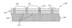
- FIG. 8is a partially schematic, cross-sectional diagram of a bonded assembly 800 , including the device assembly 100 and the carrier assembly 500 of FIG. 7 , configured in accordance with an embodiment of the present technology.
- the bonded assembly 800can be formed by bringing the device assembly 100 and the carrier assembly 500 together after alignment.
- the individual SSTs 312 of the device assembly 100are contained at least partially within the individual recesses 514 of the carrier assembly 500 .
- the first bond metal 106 of the device assembly 100 and the second bond metal 206 of the carrier assembly 500combine to form a bond metal structure 818 , which bonds the SST's 312 to the recesses 514 .
- the bond metal structure 818may be formed in a high temperature and pressure environment to facilitate bonding.
- the resulting bonded assembly 800includes a discontinuous bond 820 composed of individual bond sections or segments 821 between the SSTs 312 and the bond metal structure 818 in the recesses 514 .
- the projections 516 of the carrier assembly 500 that separate the recesses 514are not bonded to the device assembly 100 , and each individual projection 516 represents a discontinuity between the segments 821 of the discontinuous bond 820 .
- FIG. 9is a partially schematic, cross-sectional diagram of the bonded assembly 800 shown in FIG. 8 after the device substrate 102 (not shown in FIG. 9 ) has been removed in accordance with an embodiment of the present technology.
- the device substrate 102may be removed by various semiconductor fabrication techniques including backgrinding, etching, chemical-mechanical planarization and/or other suitable removal methods.
- the bonded assembly 800includes individual SSTs 312 separated by projections 516 .
- the projections 516run across the bonded assembly 800 , as shown in the overhead view of the carrier assembly 500 in FIG. 6 , to form the dicing streets 617 .
- a dicing saw or other singulation tool(not shown in FIG.
- Dicing the bonded assembly along the streets 617does not require the saw to singulate through more than one material, e.g., the saw need only cut through the carrier substrate 208 .
- Dicing through a single materialcan reduce the stresses on the bonded assembly 800 and can limit the potential for misalignments and defects caused by the singulation process. Additionally, the present technology further reduce stresses on the bonded assembly 800 by reducing or eliminating the need to singulate through a high stress bonding material.
- FIG. 10is a partially schematic, cross-sectional diagram of the device assembly 100 of FIG. 1 and a carrier assembly 1000 in alignment prior to bonding in accordance with an embodiment of the present technology.
- the carrier assembly 1000Similar to the carrier assembly 500 of FIGS. 5 and 6 , the carrier assembly 1000 includes a plurality of recesses 1014 separated by streets or projections 1016 .
- the recesses 1014 and the projections 1016form a waffle pattern with the projections 1016 surrounding individual recesses 1014 on all sides.
- the recesses 1014 in the carrier assembly 1000may be substantially filled with the second bond metal 206 to facilitate bonding with the device assembly 100 .
- FIG. 11is a partially schematic, cross-sectional diagram of a bonded assembly 1100 including the device assembly 100 and the carrier assembly 1000 of FIG. 10 configured in accordance with an embodiment of the present technology.
- the device assembly 100is brought together with and bonded to the carrier assembly 1000 .
- the resulting bonded assembly 1100includes a bond metal structure 1018 that is formed from the first bond metal 106 of the device assembly 100 and the second bond metal 206 of the carrier assembly 1000 .
- the bond metal structure 1018bonds the transducer structure 104 of the device assembly 100 to the carrier substrate 208 with a discontinuous bond 1120 .
- the discontinuous bond 1120includes bond segments 1121 between the transducer structure 104 and the recesses 1014 .
- the projections 1016 of the carrier assembly 1000are not bonded to the device assembly 100 . Accordingly, each individual projection 1016 represents a discontinuity between the bond segments 1121 of the discontinuous bond 1120 .
- FIG. 12is a partially schematic, cross-sectional diagram of the device assembly 100 of FIGS. 3 and 4 and the carrier assembly 200 of FIG. 2 in alignment prior to bonding.
- the trenches 310 , and the SSTs 312define an inverted waffle shape, with sections of the trenches 310 surrounding each of the SSTs 312 .
- FIG. 13is a partially schematic, cross-sectional diagram of a bonded assembly 1300 including the device assembly 100 and the carrier assembly 200 of FIG. 12 configured in accordance with an embodiment of the present technology.
- the device assembly 100 and the carrier assembly 200can be aligned and brought together to form the bonded assembly 1300 .
- Bonding the device assembly 100 with the carrier assembly 200combines the first bond metal 106 with the second bond metal 206 to form a bond metal structure 1318 .
- the SSTs 312 of the device assembly 100are bonded to the carrier assembly 200 with the bond metal structure 1318 .
- the trenches 310(or at least portions of the trenches 310 ) remain open, forming a void or gap.
- the bonded assembly 1300thereby includes a discontinuous bond 1320 composed of bond segments 1321 between the SSTs 312 and the carrier assembly 200 .
- the trenches 310 that separate the SSTs 312represent a discontinuity between the bond segments 1321 of the discontinuous bond 1320 .
- the discontinuous bonds of the present disclosuredecrease the mechanical stress across the bonded assemblies.
- the projections 516 of the carrier assembly 500are not bonded to the device assembly 100 , and the projections 516 represent discontinuities in the discontinuous bond 820 . The discontinuities can decrease stress across the bonded assembly 800 and reduce or eliminate bowing and warping.
- the bonded assemblies 1100 and 1300include similar stress reducing discontinuous bonds. Accordingly, the bonded assemblies of the present disclosure can be constructed on larger substrates because the lower stresses produce smaller amounts of bowing and warping for a given size substrate. In one embodiment, for example, the bonded assemblies can be constructed on eight inch diameter substrates. These larger wafers produce economies of scale not available with smaller wafers. Although the advantages of the systems and methods of the present technology may be more pronounced with larger diameter substrates, the advantages may also be present in smaller substrates. Accordingly, in other embodiments, the bonded assemblies may be constructed on smaller diameter substrates as well as larger diameter substrates.
- a further advantage of embodiments of the present technologyis that the second bond metal 206 can be contained during the fabrication process.
- the recesses 514can contain the second bond metal 206 within the projections 516 .
- the distribution of the second bond metal 206can be limited to only areas where it is needed for bonding. Accordingly, the second bond metal 206 can be prevented from migrating to other areas of the carrier assembly 500 , and either interfering with other components (which can cause defects, such as short circuits), or creating waste by migrating to areas not used for bonding.
- systems and methods in accordance with embodiments of the present disclosureincrease the efficiency and throughput with which SSTs and/or other semiconductor devices are manufactured.
- carrier assemblies, device assemblies and bonded assemblies disclosed hereincan include trenches, patterned recesses, and/or projections with different sizes and/or shapes. Rectangular recesses and SSTs, for example, may be used in some embodiments. Additionally, different materials may be used in place of those described herein, or additional components may be added or removed. For example, a bonding material may be applied to only one of either the carrier assembly or the device assembly prior to bonding. In particular embodiments the trenches surround a single SST.
- the smallest region enclosed by the trenchescan include multiple SSTs.
- Such a techniquecan be used, for example, in instances for which grouping multiple SSTs together without a bond discontinuity does not create an unacceptable warping and/or other effects, and/or instances for which the SSTs remain together as a functional unit after dicing.
- other embodimentsmay also exhibit such advantages and/or features, and not all embodiments need necessarily exhibit such advantages and/or features to fall within the scope of the technology. Accordingly, the disclosure and associated technology can encompass other embodiments not expressly shown or described herein.
Landscapes
- Engineering & Computer Science (AREA)
- Power Engineering (AREA)
- Microelectronics & Electronic Packaging (AREA)
- Computer Hardware Design (AREA)
- General Physics & Mathematics (AREA)
- Physics & Mathematics (AREA)
- Condensed Matter Physics & Semiconductors (AREA)
- Manufacturing & Machinery (AREA)
- Led Device Packages (AREA)
- Pressure Welding/Diffusion-Bonding (AREA)
- Dicing (AREA)
- Die Bonding (AREA)
- Pressure Sensors (AREA)
- Element Separation (AREA)
Abstract
Description
- This application is a continuation of U.S. application Ser. No. 14/738,663, filed Jun. 12, 2015, which is a continuation of U.S. application Ser. No. 14/305,387, filed Jun. 16, 2014, now U.S. Pat. No. 9,059,380, which is a divisional of U.S. application Ser. No. 13/220,462 filed Aug. 29, 2011, now U.S. Pat. No. 8,754,424, each of which is incorporated herein by reference.
- The present technology is directed generally to discontinuous bonds for semiconductor devices, and associated systems and methods. Discontinuous bonds in accordance with the present technology are suitable for solid-state transducers, including light-emitting diodes.
- Solid state transducer devices include light-emitting diodes (“LEDs”), organic light emitting diodes (“OLEDs”), and polymer light-emitting diodes (“PLEDS”). The energy efficiency and small size of solid state transducer devices has led to the proliferation of these devices in a multitude of products. Televisions, computer monitors, mobile phones, digital cameras, and other electronic devices utilize LEDs for image generation, object illumination (e.g., camera flashes) and/or backlighting. LEDs are also used for signage, indoor and outdoor lighting, traffic lights, and other types of illumination. Improved fabrication techniques for these semiconductor devices have both lowered device cost and increased device efficiency.
- Manufacturing processes for solid-state transducer devices and other semiconductor devices often include the use of multiple substrates. In one conventional method, semiconductor fabrication techniques are used to construct LEDs on a device substrate. A bonding material is then used to bond the device substrate to a carrier substrate, with the LEDs sandwiched therebetween. The device substrate can then be removed and the carrier substrate with the attached LEDs can be further processed to singulate individual LEDs.
- Although this fabrication method can yield reasonable results, the bonding process can produce significant stresses on the substrates and the attached LEDs. These stresses can flex and bow the substrates causing, warping, delamination or other separations, and/or can lead to misalignments during the singulation process. Additionally, singulating the LEDs through both the bonding material and the substrate can create significant stresses and complicate the singulation process. Accordingly, there is a need for a solid-state transducer device and a method of fabrication that can avoid these limitations.
FIG. 1 is a partially schematic, cross-sectional diagram of a portion of a device assembly configured in accordance with an embodiment of the present technology.FIG. 2 is a partially schematic, cross-sectional diagram of a portion of a carrier assembly configured in accordance with an embodiment of the present technology.FIG. 3 is a partially schematic, cross-sectional diagram of the device assembly ofFIG. 1 having a pattern in accordance with an embodiment of the present technology.FIG. 4 is a partially schematic, top plan view of the device assembly ofFIG. 3 .FIG. 5 is a partially schematic, cross-sectional diagram of a patterned carrier assembly configured in accordance with an embodiment of the present technology.FIG. 6 is a partially schematic, top plan view of the carrier assembly ofFIG. 5 .FIG. 7 is a partially schematic, cross-sectional diagram of the device assembly and the carrier assembly ofFIGS. 3 and 5 positioned in alignment prior to bonding.FIG. 8 is a partially schematic, cross-sectional diagram of a bonded assembly configured in accordance with an embodiment of the present technology.FIG. 9 is a partially schematic, cross-sectional diagram of the bonded assembly ofFIG. 8 after the device substrate has been removed in accordance with an embodiment of the present technology.FIG. 10 is a partially schematic, cross-sectional diagram of a device assembly and a carrier assembly prior to formation of a bonded assembly in accordance with an embodiment of the present technology.FIG. 11 is a partially schematic, cross-sectional diagram of a bonded assembly configured in accordance with an embodiment of the present technology.FIG. 12 is a partially schematic, cross-sectional diagram of a device assembly and a carrier assembly prior to formation of a bonded assembly in accordance with another embodiment of the present technology.FIG. 13 is a partially schematic, cross-sectional diagram of a bonded assembly configured in accordance with an embodiment of the present technology.- Specific details of several embodiments of wafer-level assemblies for semiconductor devices and associated systems and methods are described below. The embodiments below include solid-state transducers (“SSTs”). However, other embodiments of the presently disclosed technology may include other semiconductor devices, such as photocells, diodes, transistors, integrated circuits, etc. The term “SST” generally refers to solid-state devices that include a semiconductor material as the active medium to convert electrical energy into electromagnetic radiation in the visible, ultraviolet, infrared, and/or other spectra. For example, SST devices include solid-state light emitters (e.g., LEDs, laser diodes, etc.) and/or other sources of emission other than electrical filaments, plasmas, or gases. The term SST can also include solid-state devices that convert electromagnetic radiation into electricity. Additionally, depending upon the context in which it is used, the term “substrate” can refer to a wafer-level substrate or to a singulated device-level substrate. A person skilled in the relevant art will also understand that the technology may have additional embodiments, and that the technology may be practiced without several of the details of the embodiments described below with reference to
FIGS. 1-13 . FIG. 1 is a partially schematic, cross-sectional diagram of a portion of a wafer-level assembly, ordevice assembly 100 having adevice substrate 102, atransducer structure 104 and afirst bond metal 106 in accordance with an embodiment of the present technology. FIG.2 is a partially schematic, cross-sectional diagram of a portion of a wafer-level assembly, orcarrier assembly 200, having acarrier substrate 208 and asecond bond metal 206 in accordance with an embodiment of the present technology. The wafer-level assemblies ofFIGS. 1 and 2 may be constructed using various semiconductor fabrication techniques. Thedevice substrate 102 and thecarrier substrate 208, for example, can be made from silicon, polycrystalline aluminum nitride, sapphire, and/or other suitable materials including both metals and non-metals. Additionally, thedevice substrate 102 and/or thecarrier substrate 208 may be a composite substrate or an engineered substrate. In such embodiments, the engineered substrate may include two or more materials bonded together, and/or materials chosen or engineered to improve fabrication or assembly of thedevice assembly 100 orcarrier assembly 200. Thetransducer structure 104 can be formed via a variety of processes, including metal organic chemical vapor deposition (“MOCVD”), molecular beam epitaxy (“MBE”), liquid phase epitaxy (“LPE”), and/or hydride vapor phase epitaxy (“HVPE”). In other embodiments, at least a portion of thetransducer structure 104 may be formed using other suitable techniques, e.g., epitaxial growth techniques. Thefirst bond metal 106 and thesecond bond metal 206 ofFIGS. 1 and 2 may be composed of any of a variety of suitable metals including copper, aluminum, gold, tin, nickel, palladium, indium, and/or various alloys including combinations of these and/or other metals. In some embodiments, thefirst bond metal 106 and thesecond bond metal 206 may be composed of the same metal or alloy. In other embodiments, thefirst bond metal 106 and thesecond bond metal 206 may be composed of different metals or alloys. Furthermore, in yet other embodiments, a bonding material other than a metal may be used in place of thebond metals FIG. 3 is a partially schematic, cross-sectional diagram of thedevice assembly 100 ofFIG. 1 after having been patterned in accordance with an embodiment of the present technology. In the illustrated embodiment, the pattern formed in thedevice assembly 100 includes a plurality oftrenches 310 formed by removing sections of thefirst bond metal 106 and thetransducer structure 104.FIG. 4 is a partially schematic, top plan view of thedevice assembly 100 ofFIG. 3 . Referring toFIGS. 3 and 4 together, thetrenches 310 can form a grid that separates thetransducer structure 104 into a plurality of solid-state transducers (“SSTs”)312. The pattern of thetrenches 310 and theSSTs 312 is shaped similarly to an inverted waffle shape, with sections or segments of thetrenches 310 surrounding each of theSSTs 312. Thetrenches 310 can be formed by positioning a mask (not shown) over the areas above theSSTs 312 and etching (e.g., wet etching, dry etching, etc.) the exposed sections of thefirst bond metal 106 and thetransducer structure 104. In other embodiments, thetrenches 310 can be formed using other suitable semiconductor fabrication techniques.FIG. 5 is a partially schematic, cross-sectional diagram of apatterned carrier assembly 500 having a pattern in accordance with an embodiment of the present technology. In the illustrated embodiment, the pattern in thecarrier assembly 500 includes a plurality of intermediate regions (e.g. recesses514) separated by raised portions orprojections 516.FIG. 6 is a partially schematic, top plan view of thecarrier assembly 500 ofFIG. 5 . Referring toFIGS. 5 and 6 together, therecesses 514 and theprojections 516 form a waffle pattern with theprojections 516 surroundingindividual recesses 514 on all sides. As will be described in further detail below, theprojections 516 can form dicingstreets 617 that can be used to singulate theSSTs 312. In some embodiments, therecesses 514 can be configured to have a depth of from about 5 to about 15 microns. In other embodiments, the depth of therecesses 514 may be smaller or larger than depths included in this range. Therecesses 514 can be formed in a manner similar to that used to form thetrenches 310 in thedevice assembly 100. A mask (not shown), for example, can be used to cover theprojections 516 of thecarrier substrate 208, and exposed sections of thecarrier substrate 208 can be etched to form therecesses 514. Therecesses 514 can include blind ends515 at least partially defined by the remainingcarrier substrate 208 and/or thesecond bond metal 206 disposed in therecesses 514 to facilitate bonding with thedevice assembly 100.FIG. 7 is a partially schematic, cross-sectional diagram of thedevice assembly 100 ofFIGS. 3 and 4 and thecarrier assembly 500 ofFIGS. 5 and 6 in alignment prior to bonding. In the illustrated embodiment, the inverted waffle pattern of thedevice assembly 100 is aligned with the waffle pattern of thecarrier assembly 500, prior to bonding. In particular, theprojections 516 of thecarrier assembly 500 are aligned to be inserted into thetrenches 310, while theSSTs 312 with attached sections of thefirst bond metal 106 are aligned to be inserted into therecesses 514. Optical alignment techniques and/or other semiconductor fabrication techniques can be used to align thedevice assembly 100 to thecarrier assembly 500 in two orthogonal directions, and can be used to position thedevice assembly 100 and thecarrier assembly 500 in parallel planes to facilitate consistent bonds between these assemblies. Additionally, the patterns of the assemblies described herein are created with suitable fabrication tolerances to allow for the assemblies to be mated. For example, theprojections 516 may be slightly narrower than thetrenches 310 to avoid an interference between these components.FIG. 8 is a partially schematic, cross-sectional diagram of a bondedassembly 800, including thedevice assembly 100 and thecarrier assembly 500 ofFIG. 7 , configured in accordance with an embodiment of the present technology. Referring toFIGS. 7 and 8 together, the bondedassembly 800 can be formed by bringing thedevice assembly 100 and thecarrier assembly 500 together after alignment. When thedevice assembly 100 and thecarrier assembly 500 are brought fully together to create the bondedassembly 800, theindividual SSTs 312 of thedevice assembly 100 are contained at least partially within theindividual recesses 514 of thecarrier assembly 500. Thefirst bond metal 106 of thedevice assembly 100 and thesecond bond metal 206 of thecarrier assembly 500 combine to form abond metal structure 818, which bonds the SST's312 to therecesses 514. Thebond metal structure 818 may be formed in a high temperature and pressure environment to facilitate bonding. The resulting bondedassembly 800 includes adiscontinuous bond 820 composed of individual bond sections orsegments 821 between theSSTs 312 and thebond metal structure 818 in therecesses 514. In particular embodiments, theprojections 516 of thecarrier assembly 500 that separate therecesses 514 are not bonded to thedevice assembly 100, and eachindividual projection 516 represents a discontinuity between thesegments 821 of thediscontinuous bond 820.FIG. 9 is a partially schematic, cross-sectional diagram of the bondedassembly 800 shown inFIG. 8 after the device substrate102 (not shown inFIG. 9 ) has been removed in accordance with an embodiment of the present technology. Thedevice substrate 102 may be removed by various semiconductor fabrication techniques including backgrinding, etching, chemical-mechanical planarization and/or other suitable removal methods. After thedevice substrate 102 has been removed, the bondedassembly 800 includesindividual SSTs 312 separated byprojections 516. Theprojections 516 run across the bondedassembly 800, as shown in the overhead view of thecarrier assembly 500 inFIG. 6 , to form the dicingstreets 617. A dicing saw or other singulation tool (not shown inFIG. 9 ) is then used to cut through thecarrier substrate 208 along the dicingstreets 617 to singulate theSSTs 312. Dicing the bonded assembly along thestreets 617 does not require the saw to singulate through more than one material, e.g., the saw need only cut through thecarrier substrate 208. Dicing through a single material can reduce the stresses on the bondedassembly 800 and can limit the potential for misalignments and defects caused by the singulation process. Additionally, the present technology further reduce stresses on the bondedassembly 800 by reducing or eliminating the need to singulate through a high stress bonding material.FIG. 10 is a partially schematic, cross-sectional diagram of thedevice assembly 100 ofFIG. 1 and acarrier assembly 1000 in alignment prior to bonding in accordance with an embodiment of the present technology. Similar to thecarrier assembly 500 ofFIGS. 5 and 6 , thecarrier assembly 1000 includes a plurality ofrecesses 1014 separated by streets orprojections 1016. Therecesses 1014 and theprojections 1016 form a waffle pattern with theprojections 1016 surroundingindividual recesses 1014 on all sides. In the illustrated embodiment, therecesses 1014 in thecarrier assembly 1000 may be substantially filled with thesecond bond metal 206 to facilitate bonding with thedevice assembly 100.FIG. 11 is a partially schematic, cross-sectional diagram of a bondedassembly 1100 including thedevice assembly 100 and thecarrier assembly 1000 ofFIG. 10 configured in accordance with an embodiment of the present technology. Referring toFIGS. 10 and 11 together, after alignment, thedevice assembly 100 is brought together with and bonded to thecarrier assembly 1000. The resulting bondedassembly 1100 includes abond metal structure 1018 that is formed from thefirst bond metal 106 of thedevice assembly 100 and thesecond bond metal 206 of thecarrier assembly 1000. Thebond metal structure 1018 bonds thetransducer structure 104 of thedevice assembly 100 to thecarrier substrate 208 with adiscontinuous bond 1120. Thediscontinuous bond 1120 includesbond segments 1121 between thetransducer structure 104 and therecesses 1014. Theprojections 1016 of thecarrier assembly 1000 are not bonded to thedevice assembly 100. Accordingly, eachindividual projection 1016 represents a discontinuity between thebond segments 1121 of thediscontinuous bond 1120.FIG. 12 is a partially schematic, cross-sectional diagram of thedevice assembly 100 ofFIGS. 3 and 4 and thecarrier assembly 200 ofFIG. 2 in alignment prior to bonding. As previously discussed, thetrenches 310, and theSSTs 312 define an inverted waffle shape, with sections of thetrenches 310 surrounding each of theSSTs 312.FIG. 13 is a partially schematic, cross-sectional diagram of a bondedassembly 1300 including thedevice assembly 100 and thecarrier assembly 200 ofFIG. 12 configured in accordance with an embodiment of the present technology. As shown inFIG. 13 , thedevice assembly 100 and thecarrier assembly 200 can be aligned and brought together to form the bondedassembly 1300. Bonding thedevice assembly 100 with thecarrier assembly 200 combines thefirst bond metal 106 with thesecond bond metal 206 to form abond metal structure 1318. Accordingly, theSSTs 312 of thedevice assembly 100 are bonded to thecarrier assembly 200 with thebond metal structure 1318. In the illustrated bondedassembly 1300, the trenches310 (or at least portions of the trenches310) remain open, forming a void or gap. The bondedassembly 1300 thereby includes adiscontinuous bond 1320 composed ofbond segments 1321 between theSSTs 312 and thecarrier assembly 200. Thetrenches 310 that separate theSSTs 312 represent a discontinuity between thebond segments 1321 of thediscontinuous bond 1320.- Conventional semiconductor fabrication techniques typically produce significant stresses across wafers that can cause the wafers to bow or warp. This in turn can cause the wafer components to separate and/or become misaligned, potentially creating immediate or delayed defects in the components. These negative effects can be especially pronounced in larger wafers in which stresses can build up over larger distances. In contrast to the foregoing conventional techniques, the discontinuous bonds of the present disclosure decrease the mechanical stress across the bonded assemblies. As discussed above, in the bonded
assembly 800, for example, theprojections 516 of thecarrier assembly 500 are not bonded to thedevice assembly 100, and theprojections 516 represent discontinuities in thediscontinuous bond 820. The discontinuities can decrease stress across the bondedassembly 800 and reduce or eliminate bowing and warping. The bondedassemblies - A further advantage of embodiments of the present technology is that the
second bond metal 206 can be contained during the fabrication process. Therecesses 514, for example, can contain thesecond bond metal 206 within theprojections 516. By containing thesecond bond metal 206 within therecesses 514, the distribution of thesecond bond metal 206 can be limited to only areas where it is needed for bonding. Accordingly, thesecond bond metal 206 can be prevented from migrating to other areas of thecarrier assembly 500, and either interfering with other components (which can cause defects, such as short circuits), or creating waste by migrating to areas not used for bonding. By reducing defects and waste, systems and methods in accordance with embodiments of the present disclosure increase the efficiency and throughput with which SSTs and/or other semiconductor devices are manufactured. - From the foregoing it will be appreciated that specific embodiments of the disclosed technology have been described herein for purposes of illustration, but that various modifications may be made without deviating from the disclosure. For example, carrier assemblies, device assemblies and bonded assemblies disclosed herein can include trenches, patterned recesses, and/or projections with different sizes and/or shapes. Rectangular recesses and SSTs, for example, may be used in some embodiments. Additionally, different materials may be used in place of those described herein, or additional components may be added or removed. For example, a bonding material may be applied to only one of either the carrier assembly or the device assembly prior to bonding. In particular embodiments the trenches surround a single SST. In other embodiments, the smallest region enclosed by the trenches can include multiple SSTs. Such a technique can be used, for example, in instances for which grouping multiple SSTs together without a bond discontinuity does not create an unacceptable warping and/or other effects, and/or instances for which the SSTs remain together as a functional unit after dicing. Moreover, while various advantages and features associated with certain embodiments have been described above in the context of those embodiments, other embodiments may also exhibit such advantages and/or features, and not all embodiments need necessarily exhibit such advantages and/or features to fall within the scope of the technology. Accordingly, the disclosure and associated technology can encompass other embodiments not expressly shown or described herein.
Claims (21)
Priority Applications (4)
| Application Number | Priority Date | Filing Date | Title |
|---|---|---|---|
| US15/159,237US10242970B2 (en) | 2011-08-29 | 2016-05-19 | Discontinuous patterned bonds for semiconductor devices and associated systems and methods |
| US16/273,579US11222874B2 (en) | 2011-08-29 | 2019-02-12 | Discontinuous patterned bonds for semiconductor devices and associated systems and methods |
| US17/570,973US11901342B2 (en) | 2011-08-29 | 2022-01-07 | Discontinuous patterned bonds for semiconductor devices and associated systems and methods |
| US18/439,441US12394765B2 (en) | 2011-08-29 | 2024-02-12 | Discontinuous patterned bonds for semiconductor devices and associated systems and methods |
Applications Claiming Priority (4)
| Application Number | Priority Date | Filing Date | Title |
|---|---|---|---|
| US13/220,462US8754424B2 (en) | 2011-08-29 | 2011-08-29 | Discontinuous patterned bonds for semiconductor devices and associated systems and methods |
| US14/305,387US9059380B2 (en) | 2011-08-29 | 2014-06-16 | Discontinuous patterned bonds for semiconductor devices and associated systems and methods |
| US14/738,663US9362259B2 (en) | 2011-08-29 | 2015-06-12 | Discontinuous patterned bonds for semiconductor devices and associated systems and methods |
| US15/159,237US10242970B2 (en) | 2011-08-29 | 2016-05-19 | Discontinuous patterned bonds for semiconductor devices and associated systems and methods |
Related Parent Applications (1)
| Application Number | Title | Priority Date | Filing Date |
|---|---|---|---|
| US14/738,663ContinuationUS9362259B2 (en) | 2011-08-29 | 2015-06-12 | Discontinuous patterned bonds for semiconductor devices and associated systems and methods |
Related Child Applications (1)
| Application Number | Title | Priority Date | Filing Date |
|---|---|---|---|
| US16/273,579ContinuationUS11222874B2 (en) | 2011-08-29 | 2019-02-12 | Discontinuous patterned bonds for semiconductor devices and associated systems and methods |
Publications (2)
| Publication Number | Publication Date |
|---|---|
| US20160336302A1true US20160336302A1 (en) | 2016-11-17 |
| US10242970B2 US10242970B2 (en) | 2019-03-26 |
Family
ID=47742351
Family Applications (7)
| Application Number | Title | Priority Date | Filing Date |
|---|---|---|---|
| US13/220,462Active2031-11-07US8754424B2 (en) | 2011-08-29 | 2011-08-29 | Discontinuous patterned bonds for semiconductor devices and associated systems and methods |
| US14/305,387ActiveUS9059380B2 (en) | 2011-08-29 | 2014-06-16 | Discontinuous patterned bonds for semiconductor devices and associated systems and methods |
| US14/738,663ActiveUS9362259B2 (en) | 2011-08-29 | 2015-06-12 | Discontinuous patterned bonds for semiconductor devices and associated systems and methods |
| US15/159,237ActiveUS10242970B2 (en) | 2011-08-29 | 2016-05-19 | Discontinuous patterned bonds for semiconductor devices and associated systems and methods |
| US16/273,579Active2032-02-12US11222874B2 (en) | 2011-08-29 | 2019-02-12 | Discontinuous patterned bonds for semiconductor devices and associated systems and methods |
| US17/570,973Active2031-10-15US11901342B2 (en) | 2011-08-29 | 2022-01-07 | Discontinuous patterned bonds for semiconductor devices and associated systems and methods |
| US18/439,441ActiveUS12394765B2 (en) | 2011-08-29 | 2024-02-12 | Discontinuous patterned bonds for semiconductor devices and associated systems and methods |
Family Applications Before (3)
| Application Number | Title | Priority Date | Filing Date |
|---|---|---|---|
| US13/220,462Active2031-11-07US8754424B2 (en) | 2011-08-29 | 2011-08-29 | Discontinuous patterned bonds for semiconductor devices and associated systems and methods |
| US14/305,387ActiveUS9059380B2 (en) | 2011-08-29 | 2014-06-16 | Discontinuous patterned bonds for semiconductor devices and associated systems and methods |
| US14/738,663ActiveUS9362259B2 (en) | 2011-08-29 | 2015-06-12 | Discontinuous patterned bonds for semiconductor devices and associated systems and methods |
Family Applications After (3)
| Application Number | Title | Priority Date | Filing Date |
|---|---|---|---|
| US16/273,579Active2032-02-12US11222874B2 (en) | 2011-08-29 | 2019-02-12 | Discontinuous patterned bonds for semiconductor devices and associated systems and methods |
| US17/570,973Active2031-10-15US11901342B2 (en) | 2011-08-29 | 2022-01-07 | Discontinuous patterned bonds for semiconductor devices and associated systems and methods |
| US18/439,441ActiveUS12394765B2 (en) | 2011-08-29 | 2024-02-12 | Discontinuous patterned bonds for semiconductor devices and associated systems and methods |
Country Status (8)
| Country | Link |
|---|---|
| US (7) | US8754424B2 (en) |
| EP (1) | EP2751831B1 (en) |
| JP (1) | JP5964970B2 (en) |
| KR (1) | KR101637105B1 (en) |
| CN (1) | CN103765556B (en) |
| SG (1) | SG11201400096PA (en) |
| TW (1) | TWI497612B (en) |
| WO (1) | WO2013032688A2 (en) |
Cited By (1)
| Publication number | Priority date | Publication date | Assignee | Title |
|---|---|---|---|---|
| US11222874B2 (en) | 2011-08-29 | 2022-01-11 | Micron Technology, Inc. | Discontinuous patterned bonds for semiconductor devices and associated systems and methods |
Families Citing this family (11)
| Publication number | Priority date | Publication date | Assignee | Title |
|---|---|---|---|---|
| US8364746B2 (en) | 2005-10-21 | 2013-01-29 | T-Mobile Usa, Inc. | System and method for determining device location in an IP-based wireless telecommunications network |
| JP2012124473A (en)* | 2010-11-15 | 2012-06-28 | Ngk Insulators Ltd | Composite substrate and method for manufacturing the same |
| TWI546979B (en)* | 2012-03-05 | 2016-08-21 | 晶元光電股份有限公司 | Parallel bonded light emitting diode device and manufacturing method thereof |
| KR101824480B1 (en)* | 2014-12-03 | 2018-03-14 | 인텔 코포레이션 | Method of fabricating an electronic package |
| US10217729B2 (en) | 2016-09-30 | 2019-02-26 | Intel Corporation | Apparatus for micro pick and bond |
| US11056611B2 (en) | 2018-09-11 | 2021-07-06 | Facebook Technologies, Llc | Mesa formation for wafer-to-wafer bonding |
| US11342479B2 (en)* | 2018-09-11 | 2022-05-24 | Facebook Technologies, Llc | Reducing bowing of materials before wafer-to-wafer bonding for LED manufacturing |
| US11145786B2 (en) | 2018-09-11 | 2021-10-12 | Facebook Technologies, Llc | Methods for wafer-to-wafer bonding |
| JP7199307B2 (en)* | 2019-05-24 | 2023-01-05 | 株式会社ディスコ | Relocation method |
| DE102021108397A1 (en)* | 2021-04-01 | 2022-10-06 | OSRAM Opto Semiconductors Gesellschaft mit beschränkter Haftung | TRANSFER PROCESS FOR OPTOELECTRONIC SEMICONDUCTOR COMPONENTS |
| WO2025017863A1 (en)* | 2023-07-19 | 2025-01-23 | 三菱電機株式会社 | Semiconductor device and method for manufacturing semiconductor device |
Citations (6)
| Publication number | Priority date | Publication date | Assignee | Title |
|---|---|---|---|---|
| US20030096640A1 (en)* | 2001-01-11 | 2003-05-22 | Bae Hyon S. | Headset docking device |
| US6864570B2 (en)* | 1993-12-17 | 2005-03-08 | The Regents Of The University Of California | Method and apparatus for fabricating self-assembling microstructures |
| US20100032701A1 (en)* | 2008-08-05 | 2010-02-11 | Sharp Kabushiki Kaisha | Nitride semiconductor light emitting device and method of manufacturing the same |
| US20100096640A1 (en)* | 2007-01-05 | 2010-04-22 | Washington, University Of | Self-assembled heterogeneous integrated optical analysis system |
| US20100244071A1 (en)* | 2009-03-26 | 2010-09-30 | Toyoda Gosei Co., Ltd. | Method of manufacturing led lamp |
| US20100289046A1 (en)* | 2009-05-14 | 2010-11-18 | Kabushiki Kaisha Toshiba | Light emitting device and method for manufacturing same |
Family Cites Families (31)
| Publication number | Priority date | Publication date | Assignee | Title |
|---|---|---|---|---|
| US5545291A (en)* | 1993-12-17 | 1996-08-13 | The Regents Of The University Of California | Method for fabricating self-assembling microstructures |
| US5622305A (en)* | 1995-05-10 | 1997-04-22 | Lucent Technologies Inc. | Bonding scheme using group VB metallic layer |
| US6969635B2 (en)* | 2000-12-07 | 2005-11-29 | Reflectivity, Inc. | Methods for depositing, releasing and packaging micro-electromechanical devices on wafer substrates |
| US5814885A (en)* | 1997-04-28 | 1998-09-29 | International Business Machines Corporation | Very dense integrated circuit package |
| JPH11186670A (en)* | 1997-12-22 | 1999-07-09 | Canon Inc | Surface type optical device and manufacturing method thereof |
| US6448109B1 (en)* | 2000-11-15 | 2002-09-10 | Analog Devices, Inc. | Wafer level method of capping multiple MEMS elements |
| US7018575B2 (en)* | 2001-09-28 | 2006-03-28 | Hrl Laboratories, Llc | Method for assembly of complementary-shaped receptacle site and device microstructures |
| US7018867B2 (en)* | 2003-02-06 | 2006-03-28 | Intel Corporation | Fabricating stacked chips using fluidic templated-assembly |
| US6962835B2 (en)* | 2003-02-07 | 2005-11-08 | Ziptronix, Inc. | Method for room temperature metal direct bonding |
| JP4580633B2 (en) | 2003-11-14 | 2010-11-17 | スタンレー電気株式会社 | Semiconductor device and manufacturing method thereof |
| WO2006054233A2 (en)* | 2004-11-19 | 2006-05-26 | Koninklijke Philips Electronics N.V. | Light-emitting device with inorganic housing |
| JP5059739B2 (en)* | 2005-03-11 | 2012-10-31 | ソウル セミコンダクター カンパニー リミテッド | Light emitting diode package having an array of light emitting cells connected in series |
| US7542301B1 (en)* | 2005-06-22 | 2009-06-02 | Alien Technology Corporation | Creating recessed regions in a substrate and assemblies having such recessed regions |
| ATE405042T1 (en) | 2005-07-20 | 2008-08-15 | Alcatel Lucent | METHOD FOR ESTIMATING THE ARRIVAL TIME OF AN ACCESS BURST AND APPARATUS |
| JP2007095413A (en) | 2005-09-28 | 2007-04-12 | Toppan Printing Co Ltd | Top emission type organic electroluminescence device |
| JP2007095414A (en) | 2005-09-28 | 2007-04-12 | Toppan Printing Co Ltd | Method for manufacturing top emission type organic electroluminescence device |
| US7829909B2 (en) | 2005-11-15 | 2010-11-09 | Verticle, Inc. | Light emitting diodes and fabrication methods thereof |
| US7880382B2 (en) | 2006-03-08 | 2011-02-01 | Toppan Printing Co., Ltd. | Organic electroluminescence panel and manufacturing method of the same |
| JP4736125B2 (en)* | 2006-03-08 | 2011-07-27 | 凸版印刷株式会社 | Organic electroluminescence panel and manufacturing method thereof |
| US9159888B2 (en) | 2007-01-22 | 2015-10-13 | Cree, Inc. | Wafer level phosphor coating method and devices fabricated utilizing method |
| CN101276863B (en) | 2007-03-29 | 2011-02-09 | 晶元光电股份有限公司 | Light-emitting diode and its manufacturing method |
| US7784794B2 (en) | 2007-07-23 | 2010-08-31 | Wesley Gary Sitton | Paper archery tuner |
| US7943942B2 (en) | 2008-03-25 | 2011-05-17 | Lattice Power (Jiangxi) Corporation | Semiconductor light-emitting device with double-sided passivation |
| WO2010020071A1 (en) | 2008-08-19 | 2010-02-25 | Lattice Power (Jiangxi) Corporation | LIGHT-EMITTING DEVICE BASED ON STRAIN-ADJUSTABLE InGaAlN FILM |
| CN102067345A (en) | 2008-08-19 | 2011-05-18 | 晶能光电(江西)有限公司 | Method for fabricating semiconductor light-emitting device with double-sided passivation |
| US8173456B2 (en)* | 2009-07-05 | 2012-05-08 | Industrial Technology Research Institute | Method of manufacturing a light emitting diode element |
| JP5534763B2 (en) | 2009-09-25 | 2014-07-02 | 株式会社東芝 | Semiconductor light emitting device manufacturing method and semiconductor light emitting device |
| JP2011124311A (en)* | 2009-12-09 | 2011-06-23 | Toshiba Corp | Manufacturing method for semiconductor light-emitting element and laminated structure |
| US10672748B1 (en)* | 2010-06-02 | 2020-06-02 | Maxim Integrated Products, Inc. | Use of device assembly for a generalization of three-dimensional heterogeneous technologies integration |
| US8198109B2 (en)* | 2010-08-27 | 2012-06-12 | Quarkstar Llc | Manufacturing methods for solid state light sheet or strip with LEDs connected in series for general illumination |
| US8754424B2 (en) | 2011-08-29 | 2014-06-17 | Micron Technology, Inc. | Discontinuous patterned bonds for semiconductor devices and associated systems and methods |
- 2011
- 2011-08-29USUS13/220,462patent/US8754424B2/enactiveActive
- 2012
- 2012-08-14KRKR1020147008174Apatent/KR101637105B1/enactiveActive
- 2012-08-14JPJP2014528423Apatent/JP5964970B2/enactiveActive
- 2012-08-14WOPCT/US2012/050768patent/WO2013032688A2/enactiveApplication Filing
- 2012-08-14SGSG11201400096PApatent/SG11201400096PA/enunknown
- 2012-08-14EPEP12827286.1Apatent/EP2751831B1/enactiveActive
- 2012-08-14CNCN201280042112.2Apatent/CN103765556B/enactiveActive
- 2012-08-22TWTW101130522Apatent/TWI497612B/enactive
- 2014
- 2014-06-16USUS14/305,387patent/US9059380B2/enactiveActive
- 2015
- 2015-06-12USUS14/738,663patent/US9362259B2/enactiveActive
- 2016
- 2016-05-19USUS15/159,237patent/US10242970B2/enactiveActive
- 2019
- 2019-02-12USUS16/273,579patent/US11222874B2/enactiveActive
- 2022
- 2022-01-07USUS17/570,973patent/US11901342B2/enactiveActive
- 2024
- 2024-02-12USUS18/439,441patent/US12394765B2/enactiveActive
Patent Citations (6)
| Publication number | Priority date | Publication date | Assignee | Title |
|---|---|---|---|---|
| US6864570B2 (en)* | 1993-12-17 | 2005-03-08 | The Regents Of The University Of California | Method and apparatus for fabricating self-assembling microstructures |
| US20030096640A1 (en)* | 2001-01-11 | 2003-05-22 | Bae Hyon S. | Headset docking device |
| US20100096640A1 (en)* | 2007-01-05 | 2010-04-22 | Washington, University Of | Self-assembled heterogeneous integrated optical analysis system |
| US20100032701A1 (en)* | 2008-08-05 | 2010-02-11 | Sharp Kabushiki Kaisha | Nitride semiconductor light emitting device and method of manufacturing the same |
| US20100244071A1 (en)* | 2009-03-26 | 2010-09-30 | Toyoda Gosei Co., Ltd. | Method of manufacturing led lamp |
| US20100289046A1 (en)* | 2009-05-14 | 2010-11-18 | Kabushiki Kaisha Toshiba | Light emitting device and method for manufacturing same |
Cited By (3)
| Publication number | Priority date | Publication date | Assignee | Title |
|---|---|---|---|---|
| US11222874B2 (en) | 2011-08-29 | 2022-01-11 | Micron Technology, Inc. | Discontinuous patterned bonds for semiconductor devices and associated systems and methods |
| US11901342B2 (en) | 2011-08-29 | 2024-02-13 | Micron Technology, Inc. | Discontinuous patterned bonds for semiconductor devices and associated systems and methods |
| US12394765B2 (en) | 2011-08-29 | 2025-08-19 | Micron Technology, Inc. | Discontinuous patterned bonds for semiconductor devices and associated systems and methods |
Also Published As
| Publication number | Publication date |
|---|---|
| CN103765556A (en) | 2014-04-30 |
| CN103765556B (en) | 2016-09-07 |
| TW201316419A (en) | 2013-04-16 |
| US9059380B2 (en) | 2015-06-16 |
| US20150357314A1 (en) | 2015-12-10 |
| WO2013032688A2 (en) | 2013-03-07 |
| WO2013032688A3 (en) | 2013-07-11 |
| US11901342B2 (en) | 2024-02-13 |
| US20220130807A1 (en) | 2022-04-28 |
| JP5964970B2 (en) | 2016-08-03 |
| US20240186298A1 (en) | 2024-06-06 |
| KR101637105B1 (en) | 2016-07-06 |
| SG11201400096PA (en) | 2014-03-28 |
| TWI497612B (en) | 2015-08-21 |
| KR20140053388A (en) | 2014-05-07 |
| JP2014529908A (en) | 2014-11-13 |
| US9362259B2 (en) | 2016-06-07 |
| EP2751831A4 (en) | 2015-04-15 |
| US8754424B2 (en) | 2014-06-17 |
| US20130049016A1 (en) | 2013-02-28 |
| EP2751831B1 (en) | 2018-05-16 |
| US11222874B2 (en) | 2022-01-11 |
| US20190189597A1 (en) | 2019-06-20 |
| US10242970B2 (en) | 2019-03-26 |
| US12394765B2 (en) | 2025-08-19 |
| US20140295594A1 (en) | 2014-10-02 |
| EP2751831A2 (en) | 2014-07-09 |
Similar Documents
| Publication | Publication Date | Title |
|---|---|---|
| US12394765B2 (en) | Discontinuous patterned bonds for semiconductor devices and associated systems and methods | |
| US11837585B2 (en) | Wafer level packaging of light emitting diodes (LEDs) | |
| JP7136834B2 (en) | Wavelength conversion light emitting device with compact light source | |
| EP3025378B1 (en) | Method of separating light emitting devices formed on a substrate wafer | |
| US9666771B2 (en) | Method of forming a wavelength converted light emitting device | |
| KR20220152284A (en) | Laser lift-off handling system with metal grid |
Legal Events
| Date | Code | Title | Description |
|---|---|---|---|
| AS | Assignment | Owner name:MORGAN STANLEY SENIOR FUNDING, INC., MARYLAND Free format text:SUPPLEMENT NO. 4 TO PATENT SECURITY AGREEMENT;ASSIGNOR:MICRON TECHNOLOGY, INC.;REEL/FRAME:042405/0909 Effective date:20170425 | |
| AS | Assignment | Owner name:JPMORGAN CHASE BANK, N.A., AS COLLATERAL AGENT, ILLINOIS Free format text:SECURITY INTEREST;ASSIGNORS:MICRON TECHNOLOGY, INC.;MICRON SEMICONDUCTOR PRODUCTS, INC.;REEL/FRAME:047540/0001 Effective date:20180703 Owner name:JPMORGAN CHASE BANK, N.A., AS COLLATERAL AGENT, IL Free format text:SECURITY INTEREST;ASSIGNORS:MICRON TECHNOLOGY, INC.;MICRON SEMICONDUCTOR PRODUCTS, INC.;REEL/FRAME:047540/0001 Effective date:20180703 | |
| STCF | Information on status: patent grant | Free format text:PATENTED CASE | |
| AS | Assignment | Owner name:MICRON TECHNOLOGY, INC., IDAHO Free format text:RELEASE BY SECURED PARTY;ASSIGNOR:MORGAN STANLEY SENIOR FUNDING, INC., AS COLLATERAL AGENT;REEL/FRAME:050702/0451 Effective date:20190731 | |
| AS | Assignment | Owner name:MICRON TECHNOLOGY, INC., IDAHO Free format text:RELEASE BY SECURED PARTY;ASSIGNOR:JPMORGAN CHASE BANK, N.A., AS COLLATERAL AGENT;REEL/FRAME:051028/0001 Effective date:20190731 Owner name:MICRON SEMICONDUCTOR PRODUCTS, INC., IDAHO Free format text:RELEASE BY SECURED PARTY;ASSIGNOR:JPMORGAN CHASE BANK, N.A., AS COLLATERAL AGENT;REEL/FRAME:051028/0001 Effective date:20190731 | |
| MAFP | Maintenance fee payment | Free format text:PAYMENT OF MAINTENANCE FEE, 4TH YEAR, LARGE ENTITY (ORIGINAL EVENT CODE: M1551); ENTITY STATUS OF PATENT OWNER: LARGE ENTITY Year of fee payment:4 |