US20160312360A1 - Atomic layer deposition chamber with funnel-shaped gas dispersion channel and gas distribution plate - Google Patents
Atomic layer deposition chamber with funnel-shaped gas dispersion channel and gas distribution plateDownload PDFInfo
- Publication number
- US20160312360A1 US20160312360A1US14/734,838US201514734838AUS2016312360A1US 20160312360 A1US20160312360 A1US 20160312360A1US 201514734838 AUS201514734838 AUS 201514734838AUS 2016312360 A1US2016312360 A1US 2016312360A1
- Authority
- US
- United States
- Prior art keywords
- gas
- coupled
- substrate processing
- channel
- processing chamber
- Prior art date
- Legal status (The legal status is an assumption and is not a legal conclusion. Google has not performed a legal analysis and makes no representation as to the accuracy of the status listed.)
- Granted
Links
Images


Classifications
- C—CHEMISTRY; METALLURGY
- C23—COATING METALLIC MATERIAL; COATING MATERIAL WITH METALLIC MATERIAL; CHEMICAL SURFACE TREATMENT; DIFFUSION TREATMENT OF METALLIC MATERIAL; COATING BY VACUUM EVAPORATION, BY SPUTTERING, BY ION IMPLANTATION OR BY CHEMICAL VAPOUR DEPOSITION, IN GENERAL; INHIBITING CORROSION OF METALLIC MATERIAL OR INCRUSTATION IN GENERAL
- C23C—COATING METALLIC MATERIAL; COATING MATERIAL WITH METALLIC MATERIAL; SURFACE TREATMENT OF METALLIC MATERIAL BY DIFFUSION INTO THE SURFACE, BY CHEMICAL CONVERSION OR SUBSTITUTION; COATING BY VACUUM EVAPORATION, BY SPUTTERING, BY ION IMPLANTATION OR BY CHEMICAL VAPOUR DEPOSITION, IN GENERAL
- C23C16/00—Chemical coating by decomposition of gaseous compounds, without leaving reaction products of surface material in the coating, i.e. chemical vapour deposition [CVD] processes
- C23C16/44—Chemical coating by decomposition of gaseous compounds, without leaving reaction products of surface material in the coating, i.e. chemical vapour deposition [CVD] processes characterised by the method of coating
- C23C16/455—Chemical coating by decomposition of gaseous compounds, without leaving reaction products of surface material in the coating, i.e. chemical vapour deposition [CVD] processes characterised by the method of coating characterised by the method used for introducing gases into reaction chamber or for modifying gas flows in reaction chamber
- C23C16/45523—Pulsed gas flow or change of composition over time
- C23C16/45525—Atomic layer deposition [ALD]
- C23C16/45544—Atomic layer deposition [ALD] characterized by the apparatus
- C—CHEMISTRY; METALLURGY
- C23—COATING METALLIC MATERIAL; COATING MATERIAL WITH METALLIC MATERIAL; CHEMICAL SURFACE TREATMENT; DIFFUSION TREATMENT OF METALLIC MATERIAL; COATING BY VACUUM EVAPORATION, BY SPUTTERING, BY ION IMPLANTATION OR BY CHEMICAL VAPOUR DEPOSITION, IN GENERAL; INHIBITING CORROSION OF METALLIC MATERIAL OR INCRUSTATION IN GENERAL
- C23C—COATING METALLIC MATERIAL; COATING MATERIAL WITH METALLIC MATERIAL; SURFACE TREATMENT OF METALLIC MATERIAL BY DIFFUSION INTO THE SURFACE, BY CHEMICAL CONVERSION OR SUBSTITUTION; COATING BY VACUUM EVAPORATION, BY SPUTTERING, BY ION IMPLANTATION OR BY CHEMICAL VAPOUR DEPOSITION, IN GENERAL
- C23C16/00—Chemical coating by decomposition of gaseous compounds, without leaving reaction products of surface material in the coating, i.e. chemical vapour deposition [CVD] processes
- C23C16/44—Chemical coating by decomposition of gaseous compounds, without leaving reaction products of surface material in the coating, i.e. chemical vapour deposition [CVD] processes characterised by the method of coating
- C23C16/4401—Means for minimising impurities, e.g. dust, moisture or residual gas, in the reaction chamber
- C23C16/4405—Cleaning of reactor or parts inside the reactor by using reactive gases
- C—CHEMISTRY; METALLURGY
- C23—COATING METALLIC MATERIAL; COATING MATERIAL WITH METALLIC MATERIAL; CHEMICAL SURFACE TREATMENT; DIFFUSION TREATMENT OF METALLIC MATERIAL; COATING BY VACUUM EVAPORATION, BY SPUTTERING, BY ION IMPLANTATION OR BY CHEMICAL VAPOUR DEPOSITION, IN GENERAL; INHIBITING CORROSION OF METALLIC MATERIAL OR INCRUSTATION IN GENERAL
- C23C—COATING METALLIC MATERIAL; COATING MATERIAL WITH METALLIC MATERIAL; SURFACE TREATMENT OF METALLIC MATERIAL BY DIFFUSION INTO THE SURFACE, BY CHEMICAL CONVERSION OR SUBSTITUTION; COATING BY VACUUM EVAPORATION, BY SPUTTERING, BY ION IMPLANTATION OR BY CHEMICAL VAPOUR DEPOSITION, IN GENERAL
- C23C16/00—Chemical coating by decomposition of gaseous compounds, without leaving reaction products of surface material in the coating, i.e. chemical vapour deposition [CVD] processes
- C23C16/44—Chemical coating by decomposition of gaseous compounds, without leaving reaction products of surface material in the coating, i.e. chemical vapour deposition [CVD] processes characterised by the method of coating
- C23C16/4401—Means for minimising impurities, e.g. dust, moisture or residual gas, in the reaction chamber
- C23C16/4408—Means for minimising impurities, e.g. dust, moisture or residual gas, in the reaction chamber by purging residual gases from the reaction chamber or gas lines
- C—CHEMISTRY; METALLURGY
- C23—COATING METALLIC MATERIAL; COATING MATERIAL WITH METALLIC MATERIAL; CHEMICAL SURFACE TREATMENT; DIFFUSION TREATMENT OF METALLIC MATERIAL; COATING BY VACUUM EVAPORATION, BY SPUTTERING, BY ION IMPLANTATION OR BY CHEMICAL VAPOUR DEPOSITION, IN GENERAL; INHIBITING CORROSION OF METALLIC MATERIAL OR INCRUSTATION IN GENERAL
- C23C—COATING METALLIC MATERIAL; COATING MATERIAL WITH METALLIC MATERIAL; SURFACE TREATMENT OF METALLIC MATERIAL BY DIFFUSION INTO THE SURFACE, BY CHEMICAL CONVERSION OR SUBSTITUTION; COATING BY VACUUM EVAPORATION, BY SPUTTERING, BY ION IMPLANTATION OR BY CHEMICAL VAPOUR DEPOSITION, IN GENERAL
- C23C16/00—Chemical coating by decomposition of gaseous compounds, without leaving reaction products of surface material in the coating, i.e. chemical vapour deposition [CVD] processes
- C23C16/44—Chemical coating by decomposition of gaseous compounds, without leaving reaction products of surface material in the coating, i.e. chemical vapour deposition [CVD] processes characterised by the method of coating
- C23C16/4412—Details relating to the exhausts, e.g. pumps, filters, scrubbers, particle traps
- C—CHEMISTRY; METALLURGY
- C23—COATING METALLIC MATERIAL; COATING MATERIAL WITH METALLIC MATERIAL; CHEMICAL SURFACE TREATMENT; DIFFUSION TREATMENT OF METALLIC MATERIAL; COATING BY VACUUM EVAPORATION, BY SPUTTERING, BY ION IMPLANTATION OR BY CHEMICAL VAPOUR DEPOSITION, IN GENERAL; INHIBITING CORROSION OF METALLIC MATERIAL OR INCRUSTATION IN GENERAL
- C23C—COATING METALLIC MATERIAL; COATING MATERIAL WITH METALLIC MATERIAL; SURFACE TREATMENT OF METALLIC MATERIAL BY DIFFUSION INTO THE SURFACE, BY CHEMICAL CONVERSION OR SUBSTITUTION; COATING BY VACUUM EVAPORATION, BY SPUTTERING, BY ION IMPLANTATION OR BY CHEMICAL VAPOUR DEPOSITION, IN GENERAL
- C23C16/00—Chemical coating by decomposition of gaseous compounds, without leaving reaction products of surface material in the coating, i.e. chemical vapour deposition [CVD] processes
- C23C16/44—Chemical coating by decomposition of gaseous compounds, without leaving reaction products of surface material in the coating, i.e. chemical vapour deposition [CVD] processes characterised by the method of coating
- C23C16/448—Chemical coating by decomposition of gaseous compounds, without leaving reaction products of surface material in the coating, i.e. chemical vapour deposition [CVD] processes characterised by the method of coating characterised by the method used for generating reactive gas streams, e.g. by evaporation or sublimation of precursor materials
- C23C16/452—Chemical coating by decomposition of gaseous compounds, without leaving reaction products of surface material in the coating, i.e. chemical vapour deposition [CVD] processes characterised by the method of coating characterised by the method used for generating reactive gas streams, e.g. by evaporation or sublimation of precursor materials by activating reactive gas streams before their introduction into the reaction chamber, e.g. by ionisation or addition of reactive species
- C—CHEMISTRY; METALLURGY
- C23—COATING METALLIC MATERIAL; COATING MATERIAL WITH METALLIC MATERIAL; CHEMICAL SURFACE TREATMENT; DIFFUSION TREATMENT OF METALLIC MATERIAL; COATING BY VACUUM EVAPORATION, BY SPUTTERING, BY ION IMPLANTATION OR BY CHEMICAL VAPOUR DEPOSITION, IN GENERAL; INHIBITING CORROSION OF METALLIC MATERIAL OR INCRUSTATION IN GENERAL
- C23C—COATING METALLIC MATERIAL; COATING MATERIAL WITH METALLIC MATERIAL; SURFACE TREATMENT OF METALLIC MATERIAL BY DIFFUSION INTO THE SURFACE, BY CHEMICAL CONVERSION OR SUBSTITUTION; COATING BY VACUUM EVAPORATION, BY SPUTTERING, BY ION IMPLANTATION OR BY CHEMICAL VAPOUR DEPOSITION, IN GENERAL
- C23C16/00—Chemical coating by decomposition of gaseous compounds, without leaving reaction products of surface material in the coating, i.e. chemical vapour deposition [CVD] processes
- C23C16/44—Chemical coating by decomposition of gaseous compounds, without leaving reaction products of surface material in the coating, i.e. chemical vapour deposition [CVD] processes characterised by the method of coating
- C23C16/455—Chemical coating by decomposition of gaseous compounds, without leaving reaction products of surface material in the coating, i.e. chemical vapour deposition [CVD] processes characterised by the method of coating characterised by the method used for introducing gases into reaction chamber or for modifying gas flows in reaction chamber
- C23C16/45502—Flow conditions in reaction chamber
- C—CHEMISTRY; METALLURGY
- C23—COATING METALLIC MATERIAL; COATING MATERIAL WITH METALLIC MATERIAL; CHEMICAL SURFACE TREATMENT; DIFFUSION TREATMENT OF METALLIC MATERIAL; COATING BY VACUUM EVAPORATION, BY SPUTTERING, BY ION IMPLANTATION OR BY CHEMICAL VAPOUR DEPOSITION, IN GENERAL; INHIBITING CORROSION OF METALLIC MATERIAL OR INCRUSTATION IN GENERAL
- C23C—COATING METALLIC MATERIAL; COATING MATERIAL WITH METALLIC MATERIAL; SURFACE TREATMENT OF METALLIC MATERIAL BY DIFFUSION INTO THE SURFACE, BY CHEMICAL CONVERSION OR SUBSTITUTION; COATING BY VACUUM EVAPORATION, BY SPUTTERING, BY ION IMPLANTATION OR BY CHEMICAL VAPOUR DEPOSITION, IN GENERAL
- C23C16/00—Chemical coating by decomposition of gaseous compounds, without leaving reaction products of surface material in the coating, i.e. chemical vapour deposition [CVD] processes
- C23C16/44—Chemical coating by decomposition of gaseous compounds, without leaving reaction products of surface material in the coating, i.e. chemical vapour deposition [CVD] processes characterised by the method of coating
- C23C16/455—Chemical coating by decomposition of gaseous compounds, without leaving reaction products of surface material in the coating, i.e. chemical vapour deposition [CVD] processes characterised by the method of coating characterised by the method used for introducing gases into reaction chamber or for modifying gas flows in reaction chamber
- C23C16/45523—Pulsed gas flow or change of composition over time
- C23C16/45525—Atomic layer deposition [ALD]
- C23C16/45527—Atomic layer deposition [ALD] characterized by the ALD cycle, e.g. different flows or temperatures during half-reactions, unusual pulsing sequence, use of precursor mixtures or auxiliary reactants or activations
- C23C16/45536—Use of plasma, radiation or electromagnetic fields
- C23C16/4554—Plasma being used non-continuously in between ALD reactions
- C—CHEMISTRY; METALLURGY
- C23—COATING METALLIC MATERIAL; COATING MATERIAL WITH METALLIC MATERIAL; CHEMICAL SURFACE TREATMENT; DIFFUSION TREATMENT OF METALLIC MATERIAL; COATING BY VACUUM EVAPORATION, BY SPUTTERING, BY ION IMPLANTATION OR BY CHEMICAL VAPOUR DEPOSITION, IN GENERAL; INHIBITING CORROSION OF METALLIC MATERIAL OR INCRUSTATION IN GENERAL
- C23C—COATING METALLIC MATERIAL; COATING MATERIAL WITH METALLIC MATERIAL; SURFACE TREATMENT OF METALLIC MATERIAL BY DIFFUSION INTO THE SURFACE, BY CHEMICAL CONVERSION OR SUBSTITUTION; COATING BY VACUUM EVAPORATION, BY SPUTTERING, BY ION IMPLANTATION OR BY CHEMICAL VAPOUR DEPOSITION, IN GENERAL
- C23C16/00—Chemical coating by decomposition of gaseous compounds, without leaving reaction products of surface material in the coating, i.e. chemical vapour deposition [CVD] processes
- C23C16/44—Chemical coating by decomposition of gaseous compounds, without leaving reaction products of surface material in the coating, i.e. chemical vapour deposition [CVD] processes characterised by the method of coating
- C23C16/455—Chemical coating by decomposition of gaseous compounds, without leaving reaction products of surface material in the coating, i.e. chemical vapour deposition [CVD] processes characterised by the method of coating characterised by the method used for introducing gases into reaction chamber or for modifying gas flows in reaction chamber
- C23C16/45561—Gas plumbing upstream of the reaction chamber
- C—CHEMISTRY; METALLURGY
- C23—COATING METALLIC MATERIAL; COATING MATERIAL WITH METALLIC MATERIAL; CHEMICAL SURFACE TREATMENT; DIFFUSION TREATMENT OF METALLIC MATERIAL; COATING BY VACUUM EVAPORATION, BY SPUTTERING, BY ION IMPLANTATION OR BY CHEMICAL VAPOUR DEPOSITION, IN GENERAL; INHIBITING CORROSION OF METALLIC MATERIAL OR INCRUSTATION IN GENERAL
- C23C—COATING METALLIC MATERIAL; COATING MATERIAL WITH METALLIC MATERIAL; SURFACE TREATMENT OF METALLIC MATERIAL BY DIFFUSION INTO THE SURFACE, BY CHEMICAL CONVERSION OR SUBSTITUTION; COATING BY VACUUM EVAPORATION, BY SPUTTERING, BY ION IMPLANTATION OR BY CHEMICAL VAPOUR DEPOSITION, IN GENERAL
- C23C16/00—Chemical coating by decomposition of gaseous compounds, without leaving reaction products of surface material in the coating, i.e. chemical vapour deposition [CVD] processes
- C23C16/44—Chemical coating by decomposition of gaseous compounds, without leaving reaction products of surface material in the coating, i.e. chemical vapour deposition [CVD] processes characterised by the method of coating
- C23C16/455—Chemical coating by decomposition of gaseous compounds, without leaving reaction products of surface material in the coating, i.e. chemical vapour deposition [CVD] processes characterised by the method of coating characterised by the method used for introducing gases into reaction chamber or for modifying gas flows in reaction chamber
- C23C16/45563—Gas nozzles
- C23C16/45565—Shower nozzles
- C—CHEMISTRY; METALLURGY
- C23—COATING METALLIC MATERIAL; COATING MATERIAL WITH METALLIC MATERIAL; CHEMICAL SURFACE TREATMENT; DIFFUSION TREATMENT OF METALLIC MATERIAL; COATING BY VACUUM EVAPORATION, BY SPUTTERING, BY ION IMPLANTATION OR BY CHEMICAL VAPOUR DEPOSITION, IN GENERAL; INHIBITING CORROSION OF METALLIC MATERIAL OR INCRUSTATION IN GENERAL
- C23C—COATING METALLIC MATERIAL; COATING MATERIAL WITH METALLIC MATERIAL; SURFACE TREATMENT OF METALLIC MATERIAL BY DIFFUSION INTO THE SURFACE, BY CHEMICAL CONVERSION OR SUBSTITUTION; COATING BY VACUUM EVAPORATION, BY SPUTTERING, BY ION IMPLANTATION OR BY CHEMICAL VAPOUR DEPOSITION, IN GENERAL
- C23C16/00—Chemical coating by decomposition of gaseous compounds, without leaving reaction products of surface material in the coating, i.e. chemical vapour deposition [CVD] processes
- C23C16/44—Chemical coating by decomposition of gaseous compounds, without leaving reaction products of surface material in the coating, i.e. chemical vapour deposition [CVD] processes characterised by the method of coating
- C23C16/455—Chemical coating by decomposition of gaseous compounds, without leaving reaction products of surface material in the coating, i.e. chemical vapour deposition [CVD] processes characterised by the method of coating characterised by the method used for introducing gases into reaction chamber or for modifying gas flows in reaction chamber
- C23C16/45582—Expansion of gas before it reaches the substrate
- C—CHEMISTRY; METALLURGY
- C23—COATING METALLIC MATERIAL; COATING MATERIAL WITH METALLIC MATERIAL; CHEMICAL SURFACE TREATMENT; DIFFUSION TREATMENT OF METALLIC MATERIAL; COATING BY VACUUM EVAPORATION, BY SPUTTERING, BY ION IMPLANTATION OR BY CHEMICAL VAPOUR DEPOSITION, IN GENERAL; INHIBITING CORROSION OF METALLIC MATERIAL OR INCRUSTATION IN GENERAL
- C23C—COATING METALLIC MATERIAL; COATING MATERIAL WITH METALLIC MATERIAL; SURFACE TREATMENT OF METALLIC MATERIAL BY DIFFUSION INTO THE SURFACE, BY CHEMICAL CONVERSION OR SUBSTITUTION; COATING BY VACUUM EVAPORATION, BY SPUTTERING, BY ION IMPLANTATION OR BY CHEMICAL VAPOUR DEPOSITION, IN GENERAL
- C23C16/00—Chemical coating by decomposition of gaseous compounds, without leaving reaction products of surface material in the coating, i.e. chemical vapour deposition [CVD] processes
- C23C16/44—Chemical coating by decomposition of gaseous compounds, without leaving reaction products of surface material in the coating, i.e. chemical vapour deposition [CVD] processes characterised by the method of coating
- C23C16/455—Chemical coating by decomposition of gaseous compounds, without leaving reaction products of surface material in the coating, i.e. chemical vapour deposition [CVD] processes characterised by the method of coating characterised by the method used for introducing gases into reaction chamber or for modifying gas flows in reaction chamber
- C23C16/45587—Mechanical means for changing the gas flow
- C23C16/45591—Fixed means, e.g. wings, baffles
- H—ELECTRICITY
- H01—ELECTRIC ELEMENTS
- H01J—ELECTRIC DISCHARGE TUBES OR DISCHARGE LAMPS
- H01J37/00—Discharge tubes with provision for introducing objects or material to be exposed to the discharge, e.g. for the purpose of examination or processing thereof
- H01J37/32—Gas-filled discharge tubes
- H01J37/32009—Arrangements for generation of plasma specially adapted for examination or treatment of objects, e.g. plasma sources
- H01J37/32357—Generation remote from the workpiece, e.g. down-stream
- H—ELECTRICITY
- H01—ELECTRIC ELEMENTS
- H01J—ELECTRIC DISCHARGE TUBES OR DISCHARGE LAMPS
- H01J37/00—Discharge tubes with provision for introducing objects or material to be exposed to the discharge, e.g. for the purpose of examination or processing thereof
- H01J37/32—Gas-filled discharge tubes
- H01J37/32431—Constructional details of the reactor
- H01J37/3244—Gas supply means
- H01J37/32449—Gas control, e.g. control of the gas flow
- H—ELECTRICITY
- H01—ELECTRIC ELEMENTS
- H01J—ELECTRIC DISCHARGE TUBES OR DISCHARGE LAMPS
- H01J37/00—Discharge tubes with provision for introducing objects or material to be exposed to the discharge, e.g. for the purpose of examination or processing thereof
- H01J37/32—Gas-filled discharge tubes
- H01J37/32431—Constructional details of the reactor
- H01J37/32798—Further details of plasma apparatus not provided for in groups H01J37/3244 - H01J37/32788; special provisions for cleaning or maintenance of the apparatus
- H01J37/32816—Pressure
- H01J37/32834—Exhausting
Definitions
- Embodiments of the disclosuregenerally relate to apparatus and methods for atomic layer deposition.
- VLSIvery large scale integration
- ULSIultra large scale integration
- the multilevel interconnects that lie at the heart of VLSI and ULSI technologyuse precise processing of high aspect ratio features, such as vias and other interconnects. Reliable formation of these interconnects is very important to VLSI and ULSI success and to the continued effort to increase circuit density and quality of individual substrates.
- interconnectssuch as vias, trenches, contacts, and other features, as well as the dielectric materials between
- the widths of interconnectsdecrease while the thickness of the dielectric layers remain substantially constant, resulting in increased height-to-width aspect ratios of the features.
- Many traditional deposition processeshave difficulty filling submicron structures where the aspect ratio exceeds 4:1, and particularly where the aspect ratio exceeds 10:1. Therefore, there is a great amount of ongoing effort being directed at the formation of substantially void-free and seam-free submicron features having high aspect ratios.
- Atomic layer depositionis a deposition technique being explored for the deposition of material layers over features having high aspect ratios.
- ALDAtomic layer deposition
- One example of an ALD processincludes the sequential introduction of pulses of gases.
- one cycle for the sequential introduction of pulses of gasesmay contain a pulse of a first reactant gas, followed by a pulse of a purge gas and/or a pump evacuation, followed by a pulse of a second reactant gas, and followed by a pulse of a purge gas and/or a pump evacuation.
- gasas used herein is defined to include a single gas or a plurality of gases.
- Sequential introduction of separate pulses of the first reactant and the second reactantmay result in the alternating self-limiting absorption of monolayers of the reactants on the surface of the substrate and, thus, forms a monolayer of material for each cycle.
- the cyclemay be repeated to a desired thickness of the deposited material.
- a pulse of a purge gas and/or a pump evacuation between the pulses of the first reactant gas and the pulses of the second reactant gasserves to reduce the likelihood of gas phase reactions of the reactants due to excess amounts of the reactants remaining in the chamber.
- precursors and gasesare delivered using a funnel lid through which precursor is distributed through multiple injectors above a funnel shaped lid.
- the injectorsgenerate a circular motion of the injected gas which distributes through the funnel profile at the center of the lid.
- the rotational inertia of the gas/ALD precursor moleculesdistributes the molecules from center to edge resulting in improved uniformity deposition.
- the inventorshave observed a donut-shaped deposition profile near the center of the substrate being processed. The donut-shaped deposition profile is believed to be caused by the funnel shape of the lid and can lead to integration issues for customers.
- the inventorshave provided improved apparatus and methods for ALD processing of a substrate.
- a substrate processing chamberincludes: a chamber body; a chamber lid assembly having a housing enclosing a central channel that extends along a central axis and has an upper portion and a lower portion; a lid plate coupled to the housing and having a contoured bottom surface that extends downwardly and outwardly from a central opening coupled to the lower portion of the central channel to a peripheral portion of the lid plate; and a gas distribution plate disposed below the lid plate and having a plurality of apertures disposed through the gas distribution plate.
- a substrate processing chamberincludes: a chamber body; a chamber lid assembly having a housing enclosing a central channel that extends along a central axis and has an upper portion and a lower portion; a lid plate coupled to the housing and having a contoured bottom surface that extends downwardly and outwardly from a central opening coupled to the lower portion of the central channel to a peripheral portion of the lid plate; a gas distribution plate disposed below the lid plate and having a plurality of apertures disposed through the gas distribution plate; a remote plasma source fluidly coupled to the central channel; an isolation collar coupled between the remote plasma source and the housing, wherein the isolation collar has an inner channel extending through the isolation collar to fluidly couple the remote plasma source and the central channel; an exhaust conduit coupled to the isolation collar at a first end and to a main pumping channel at a second end; and a valve coupled to the exhaust conduit to selectively open or close the exhaust conduit.
- a method of processing a substrateincludes: flowing a first process gas into a gas dispersion channel and a reaction zone of a process chamber; flowing the first process gas through a plurality of apertures in a gas distribution plate disposed in the reaction zone and onto the substrate; flowing a cleaning gas into the gas dispersion channel and the reaction zone; exhausting the cleaning gas via an exhaust system; flowing a second process gas into the gas dispersion channel and the reaction zone; flowing the second process gas through the plurality of apertures in the gas distribution plate and onto the substrate; flowing the cleaning gas into the gas dispersion channel and the reaction zone; and exhausting the cleaning gas via the exhaust system.
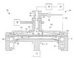
- FIG. 1depicts a schematic view of a process chamber in accordance with some embodiments of the present disclosure.
- FIG. 2depicts a schematic cross-sectional view of a process chamber in accordance with some embodiments of the present disclosure.
- FIG. 3depicts a schematic cross-sectional view of a lid assembly in accordance with some embodiments of the present disclosure.
- FIGS. 4A-Cdepict schematic views of apertures disposed through a gas distribution plate in accordance with embodiments of the present disclosure.
- FIG. 5depicts a flowchart illustrating a method of processing a substrate in accordance to some embodiments of the present disclosure.
- Embodiments of the present disclosureprovide apparatus and methods that may be used to clean substrate processing chambers, such as an atomic layer deposition (ALD) chamber, and to deposit materials during, for example, an ALD process.
- substrate processing chamberssuch as an atomic layer deposition (ALD) chamber
- Embodimentsinclude substrate processing chambers and gas delivery systems which include a remote plasma source and a gas distribution plate. Other embodiments provide methods for depositing materials using these gas delivery systems during ALD processes.
- suitable processing chambers for incorporation of the apparatuses described hereininclude high dielectric constant (i.e., high k) and metal ALD deposition chambers available from Applied Materials, Inc., of Santa Clara, Calif.
- the following process chamber descriptionis provided for context and exemplary purposes, and should not be interpreted or construed as limiting the scope of the disclosure.
- FIG. 1is a schematic view of a substrate processing chamber (process chamber 100 ) including a gas delivery system 130 adapted for ALD processes in accordance with some embodiments of the present disclosure.
- FIG. 2is a cross-sectional view of the process chamber 100 .
- Process chamber 100includes a chamber body 102 having a processing volume within the chamber body 102 and beneath the chamber lid assembly 132 .
- Slit valve 108 in the process chamber 100provides access for a robot (not shown) to deliver and retrieve a substrate 110 , such as a 200 mm or 300 mm semiconductor wafer or a glass substrate, to and from the process chamber 100 .
- a chamber liner 177is disposed along the walls of the process chamber 100 to protect the chamber from corrosive gases used during processing/cleaning.
- a substrate support 112supports the substrate 110 on a substrate receiving surface 111 in the process chamber 100 .
- the substrate support 112is mounted to a lift motor 114 for raising and lowering the substrate support 112 and the substrate 110 disposed on the substrate support.
- a lift plate 116(shown in FIG. 2 ), connected to a lift motor 118 , is mounted in the process chamber 100 to raise and lower lift pins 120 movably disposed through the substrate support 112 .
- the lift pins 120raise and lower the substrate 110 over the surface of the substrate support 112 .
- the substrate support 112may include a vacuum chuck (not shown), an electrostatic chuck (not shown), or a clamp ring (not shown) for securing the substrate 110 to the substrate support 112 during a deposition process.
- the temperature of the substrate support 112may be adjusted to control the temperature of the substrate 110 .
- substrate support 112may be heated using an embedded heating element, such as a resistive heater (not shown), or may be heated using radiant heat, such as heating lamps (not shown) disposed above the substrate support 112 .
- a purge ring 122may be disposed on the substrate support 112 to define a purge channel 124 which provides a purge gas to a peripheral portion of the substrate 110 to prevent deposition on the peripheral portion of the substrate 110 .
- Gas delivery system 130is disposed at an upper portion of the chamber body 102 to provide a gas, such as a process gas and/or a purge gas, to process chamber 100 .
- a vacuum system(not shown) is in communication with a pumping channel 179 to evacuate any desired gases from the process chamber 100 and to help maintain a desired pressure or pressure range inside the process chamber 100 .
- the chamber lid assembly 132includes a gas dispersion channel 134 extending through a central portion of the chamber lid assembly 132 .
- the gas dispersion channel 134extends perpendicularly toward the substrate receiving surface 111 and also extends along a central axis 133 of the gas dispersion channel 134 , through lid plate 170 , and to lower surface 160 .
- an upper portion of the gas dispersion channel 134is substantially cylindrical along central axis 133 and a lower portion of the gas dispersion channel 134 tapers away from central axis 133 .
- the lower surface 160is sized and shaped to substantially cover the substrate 110 disposed on the substrate receiving surface 111 of the substrate support 112 .
- the lower surface 160tapers from an outer edge of the lid plate 170 towards the gas dispersion channel 134 .
- the gas delivery system 130may provide one or more gasses to the gas dispersion channel 134 to process the substrate 110 .
- the gas delivery system 130may be coupled to the gas dispersion channel 134 via one gas inlet.
- the gas delivery systemmay be coupled to the gas dispersion channel 134 via a plurality of inlets.
- circular gas flow 174which illustrates the flow of process gases through the gas dispersion channel 134 , may contain various types of flow patterns.
- processing gasesmay be forced to make revolutions around central axis 133 of gas dispersion channel 134 while passing through the dispersion channel.
- the circular gas flow 174may contain various types of circular flow patterns, such as a vortex pattern, a helix pattern, a spiral pattern, or derivatives thereof.
- the process chamber 100further includes a gas distribution plate 125 having a plurality of apertures 126 disposed through the gas distribution plate 125 .
- the gas distribution plate 125extends to the surface of the gas dispersion channel 134 such that the only pathway from the gas dispersion channel 134 to the substrate is through the plurality of apertures 126 of the gas distribution plate 125 .
- the gas distribution plate 125advantageously creates a choked flow of gas through the gas distribution plate 125 resulting in a more uniform deposition on the substrate 110 and, thus, substantially eliminating the donut-shaped deposition caused by the rotational flow of gas.
- the gas distribution plate 125is formed of a non-corrosive ceramic material such as, for example, aluminum oxide or aluminum nitride.
- each of the plurality of apertures 126may have an equivalent fluid conductance.
- a density of the plurality of apertures 126(e.g., the number of apertures or the size of the openings of the apertures per unit area) may vary across the gas distribution plate 125 to achieve a desired deposition profile on the substrate 110 . For example, a higher density of apertures 126 may be disposed at a center of the gas distribution plate 125 to increase the deposition rate at the center of the substrate relative to the edge of the substrate to further improve deposition uniformity.
- FIGS. 4A-Cdepict different non-limiting embodiments of profiles of the plurality of apertures 126 .
- the aperture 126is a cylindrical through hole having curved edges 402 that surround the aperture.
- the aperture 126is a through hole having an upper portion 404 that tapers inwardly toward a center of the aperture, a cylindrical center portion 405 extending perpendicularly to an upper surface 127 of the gas distribution plate 125 , and a lower portion 406 that tapers outwardly from the center of the aperture.
- FIG. 4Athe aperture 126 is a cylindrical through hole having curved edges 402 that surround the aperture.
- the aperture 126is a through hole having an upper portion 404 that tapers inwardly toward a center of the aperture, a cylindrical center portion 405 extending perpendicularly to an upper surface 127 of the gas distribution plate 125 , and a lower portion 406 that tapers outwardly from the center of the aperture.
- the aperture 126is a through hole having an upper portion 408 having a countersunk hole, a cylindrical center portion 409 extending perpendicularly to the upper surface 127 of the gas distribution plate 125 , and a lower portion 410 that tapers outwardly from the center of the aperture.
- Other profiles of the plurality of apertures 126may alternatively be used to achieve optimal deposition uniformity during processing of the substrate 110 .
- the inventorsbelieve that the diameter of gas dispersion channel 134 , which is constant from the upper portion of gas dispersion channel 134 to a first point along central axis 133 and increasing from the first point to lower portion 135 of gas dispersion channel 134 , allows less of an adiabatic expansion of a gas through gas dispersion channel 134 which helps to control the temperature of the process gas contained in the circular gas flow 174 .
- a sudden adiabatic expansion of a gas delivered into gas dispersion channel 134may result in a drop in the temperature of the gas which may cause condensation of the gas and formation of droplets.
- Gas dispersion channel 134that gradually tapers is believed to provide less of an adiabatic expansion of a gas. Therefore, more heat may be transferred to or from the gas, and, thus, the temperature of the gas may be more easily controlled by controlling the temperature of chamber lid assembly 132 .
- Gas dispersion channel 134may gradually taper and contain one or more tapered inner surfaces, such as a tapered straight surface, a concave surface, a convex surface, or combinations thereof or may contain sections of one or more tapered inner surfaces (i.e., a portion tapered and a portion non-tapered).
- the upper portion of the gas dispersion channel 134is defined by an insert 300 disposed in an inner region of a housing 375 .
- the insert 300includes a cap 302 at an upper portion of the insert 300 and a central passageway that at least partially defines the gas dispersion channel 134 .
- the cap 302extends over the housing 375 to hold the insert 300 in place.
- the insert 300 and cap 302include a plurality of o-rings 385 disposed between the insert 300 and the housing 375 to ensure proper sealing.
- the insert 300includes a plurality of circumferential apertures which, when the insert 300 is inserted into the housing 375 , form a corresponding plurality of circumferential channels 360 , 365 , 370 .
- the plurality of circumferential channels 360 , 365 , 370are fluidly coupled to the gas dispersion channel 134 via a corresponding plurality of holes 340 , 345 , 350 .
- the gas delivery system 130is coupled to the gas dispersion channel 134 via a plurality of gas feed lines 310 , 315 , 320 .
- the gas feed lines gas feed lines 310 , 315 , 320are fluidly coupled to the plurality of circumferential channels 360 , 365 , 370 to provide one or more gases to the gas dispersion channel 134 .
- the process chamber 100further includes a chamber cleaning system including a remote plasma source (RPS) 190 , an isolation collar 192 coupled to the RPS 190 at one end and the cap 302 at an opposite end, a heater plate 198 coupled to an upper surface of the lid plate 170 , and a cleaning gas (i.e., purge gas) source 197 fluidly coupled to the RPS 190 .
- the cleaning gas sourcemay include any gas suitable for forming a plasma to clean the process chamber 100 .
- the cleaning gasmay be nitrogen trifluoride (NF 3 ).
- the isolation collar 192includes an inner channel 193 that is fluidly coupled to the gas dispersion channel 134 through a plurality of holes 285 disposed in a central portion of the cap 302 to flow a plasma from the RPS 190 through the gas dispersion channel 134 and into the reaction zone 164 .
- the heater plate 198may be formed of stainless steel and include a plurality of resistive heating elements dispersed throughout the plate.
- a cleaning gasis flowed through the gas dispersion channel 134 and the reaction zone 164 after a first gas is provided to the gas dispersion channel 134 by the gas delivery system 130 to quickly purge the first gas from the gas dispersion channel 134 and the reaction zone 164 .
- a second gasis provided by the gas delivery system 130 to the gas dispersion channel 134 and the cleaning gas is again flowed through the gas dispersion channel 134 to the reaction zone 164 to quickly purge the second gas from the gas dispersion channel 134 and the reaction zone 164 .
- the addition of the gas distribution plate 125chokes the flow of the cleaning gas to the pumping channel 179 and prolongs the cleaning process.
- an exhaust system 180having an exhaust conduit 184 coupled to the isolation collar 192 at a first end 186 and to the pumping channel 179 at a second end 188 .
- a valve 182is disposed in the exhaust conduit 184 to selectively fluidly couple the exhaust conduit 184 to the inner channel 193 .
- the valve 182may be a plunger type valve having a plunger 202 that is moveable between a first position (shown in FIG. 2 ) to fluidly couple the exhaust conduit 184 to the inner channel 193 and a second position to seal off the exhaust conduit 184 from the inner channel 193 .
- the valve 182is opened and the cleaning gas is rapidly exhausted to the pumping channel 179 .
- the isolation collar 192may be formed of any material that is non-reactive with the cleaning gas being used. In some embodiments, the isolation collar 192 may be formed of aluminum when the cleaning gas is NF 3 . In some embodiments, the isolation collar 192 and the insert 300 may be formed of aluminum and coated with a coating to prevent corrosion of the isolation collar 192 and the insert 300 from corrosive gases when used. For example, the coating may be formed of nickel or aluminum oxide.
- the RPS 190operates at a temperature less than or equal to about 40° C.
- a thermal isolation ring 394is disposed between the isolation collar 192 and the cap 302 .
- the thermal isolation ring 394is formed of a metal with low thermal conductivity (e.g., lower than the thermal conductivity of the isolation collar 192 and the cap 302 ).
- an o-ring 385may also be disposed between the isolation collar 192 and the cap 302 to further reduce the contact area between the isolation collar 192 and the cap 302 .
- the combination of the thermal isolation ring 394 and the o-ring 385acts as a thermal choke to ensure that the heat generated in the process chamber 100 does not adversely affect the RPS 190 .
- the process chamber 100may include a differential pumping line 250 to ensure that any process gases or byproducts trapped between o-rings 385 are exhausted to the pumping channel 179 .
- the differential pumping line 250is coupled to the lid plate 170 at a first end and to the housing 375 at a second end opposite the first end.
- the differential pumping lineis fluidly coupled to the gas dispersion channel 134 and to one or more channels 260 formed at areas between two or more o-rings 385 .
- the valve 182is opened to exhaust the gas dispersion channel 134 , the differential pumping line exhausts gases trapped between o-rings 385 .
- a portion of lower surface 160 of chamber lid assembly 132may be contoured or angled downwardly and outwardly from a central opening coupled to the gas dispersion channel 134 to a peripheral portion of chamber lid assembly 132 to help provide an improved velocity profile of a gas flow from gas dispersion channel 134 across the surface of substrate 110 (i.e., from the center of the substrate to the edge of the substrate).
- Lower surface 160may contain one or more surfaces, such as a straight surface, a concave surface, a convex surface, or combinations thereof. In one embodiment, lower surface 160 is convexly funnel-shaped.
- lower surface 160is downwardly and outwardly sloping toward an edge of the substrate receiving surface 111 to help reduce the variation in the velocity of the process gases traveling between lower surface 160 of chamber lid assembly 132 and substrate 110 while assisting to provide uniform exposure of the surface of substrate 110 to a reactant gas.
- the components and parts of chamber lid assembly 132may contain materials such as stainless steel, aluminum, nickel-plated aluminum, nickel, alloys thereof, or other suitable materials.
- lid plate 170may be independently fabricated, machined, forged, or otherwise made from a metal, such as aluminum, an aluminum alloy, steel, stainless steel, alloys thereof, or combinations thereof.
- inner surface 131 of gas dispersion channel 134 and lower surface 160 of chamber lid assembly 132may contain a mirror polished surface to help a flow of a gas along gas dispersion channel 134 and lower surface 160 of chamber lid assembly 132 .
- substrate 110is delivered to process chamber 100 through slit valve 108 by a robot (not shown).
- Substrate 110is positioned on substrate support 112 through cooperation of lift pins 120 and the robot.
- Substrate support 112raises substrate 110 into close opposition to a lower surface of the gas distribution plate 125 .
- a first gas flowmay be injected into gas dispersion channel 134 of process chamber 100 by the gas delivery system 130 together or separately (i.e., pulses) with a second gas flow.
- the first gas flowmay contain a continuous flow of a purge gas from a purge gas source and pulses of a reactant gas from a reactant gas source or may contain pulses of a reactant gas from the reactant gas source and pulses of a purge gas from the purge gas source.
- the second gas flowmay contain a continuous flow of a purge gas from a purge gas source and pulses of a reactant gas from a reactant gas source or may contain pulses of a reactant gas from a reactant gas source and pulses of a purge gas from a purge gas source.
- the circular gas flow 174travels through gas dispersion channel 134 and subsequently through the plurality of apertures 126 in the gas distribution plate 125 .
- the gasis then deposited on the surface of substrate 110 .
- Lower surface 160 of chamber lid assembly 132which is downwardly sloping, helps reduce the variation of the velocity of the gas flow across the surface of gas distribution plate 125 .
- Excess gas, by-products, etc.flow into the pumping channel 179 and are then exhausted from process chamber 100 .
- the heater plate 198may heat the chamber lid assembly 132 to a predetermined temperature to heat any solid byproducts that have accumulated on walls of the process chamber 100 (or a processing kit disposed in the chamber). As a result, any accumulated solid byproducts are vaporized.
- the vaporized byproductsare evacuated by a vacuum system (not shown) and pumping channel 179 .
- the predetermined temperatureis greater than or equal to 150° C.
- FIG. 5illustrates a method 500 of processing a substrate in accordance with some embodiments of the present disclosure.
- a first process gasis flowed from the gas delivery system 130 into the gas dispersion channel 134 and the reaction zone 164 .
- the first process gasis flowed through the plurality of apertures 126 in the gas distribution plate 125 and onto the substrate 110 .
- a cleaning gasis flowed into the gas dispersion channel 134 and the reaction zone 164 to purge the first process gas.
- the cleaning gasis exhausted via the exhaust system 180 .
- a second process gasis flowed into the gas dispersion channel 134 and the reaction zone 164 .
- the second process gasis flowed through the plurality of apertures 126 in the gas distribution plate 125 and onto the substrate 110 .
- the cleaning gasis flowed into the gas dispersion channel 134 and the reaction zone 164 to purge the second process gas.
- the cleaning gasis exhausted via the exhaust system 180 .
Landscapes
- Chemical & Material Sciences (AREA)
- Engineering & Computer Science (AREA)
- Metallurgy (AREA)
- Chemical Kinetics & Catalysis (AREA)
- Materials Engineering (AREA)
- Mechanical Engineering (AREA)
- General Chemical & Material Sciences (AREA)
- Organic Chemistry (AREA)
- Physics & Mathematics (AREA)
- Plasma & Fusion (AREA)
- Analytical Chemistry (AREA)
- Electromagnetism (AREA)
- Chemical Vapour Deposition (AREA)
- Crystals, And After-Treatments Of Crystals (AREA)
Abstract
Description
- This application claims benefit of U.S. provisional patent application Ser. No. 62/151,180, filed Apr. 22, 2015, which is herein incorporated by reference in its entirety.
- Embodiments of the disclosure generally relate to apparatus and methods for atomic layer deposition.
- Reliably producing submicron and smaller features is one of the key technologies for the next generation of very large scale integration (VLSI) and ultra large scale integration (ULSI) of semiconductor devices. However, as the fringes of circuit technology are pressed, the shrinking dimensions of interconnects in VLSI and ULSI technology have placed additional demands on the processing capabilities. The multilevel interconnects that lie at the heart of VLSI and ULSI technology use precise processing of high aspect ratio features, such as vias and other interconnects. Reliable formation of these interconnects is very important to VLSI and ULSI success and to the continued effort to increase circuit density and quality of individual substrates.
- As circuit densities increase, the widths of interconnects, such as vias, trenches, contacts, and other features, as well as the dielectric materials between, decrease while the thickness of the dielectric layers remain substantially constant, resulting in increased height-to-width aspect ratios of the features. Many traditional deposition processes have difficulty filling submicron structures where the aspect ratio exceeds 4:1, and particularly where the aspect ratio exceeds 10:1. Therefore, there is a great amount of ongoing effort being directed at the formation of substantially void-free and seam-free submicron features having high aspect ratios.
- Atomic layer deposition (ALD) is a deposition technique being explored for the deposition of material layers over features having high aspect ratios. One example of an ALD process includes the sequential introduction of pulses of gases. For instance, one cycle for the sequential introduction of pulses of gases may contain a pulse of a first reactant gas, followed by a pulse of a purge gas and/or a pump evacuation, followed by a pulse of a second reactant gas, and followed by a pulse of a purge gas and/or a pump evacuation. The term “gas” as used herein is defined to include a single gas or a plurality of gases. Sequential introduction of separate pulses of the first reactant and the second reactant may result in the alternating self-limiting absorption of monolayers of the reactants on the surface of the substrate and, thus, forms a monolayer of material for each cycle. The cycle may be repeated to a desired thickness of the deposited material. A pulse of a purge gas and/or a pump evacuation between the pulses of the first reactant gas and the pulses of the second reactant gas serves to reduce the likelihood of gas phase reactions of the reactants due to excess amounts of the reactants remaining in the chamber.
- In some chamber designs for ALD processing, precursors and gases are delivered using a funnel lid through which precursor is distributed through multiple injectors above a funnel shaped lid. The injectors generate a circular motion of the injected gas which distributes through the funnel profile at the center of the lid. The rotational inertia of the gas/ALD precursor molecules distributes the molecules from center to edge resulting in improved uniformity deposition. However, in some applications, the inventors have observed a donut-shaped deposition profile near the center of the substrate being processed. The donut-shaped deposition profile is believed to be caused by the funnel shape of the lid and can lead to integration issues for customers.
- Therefore, the inventors have provided improved apparatus and methods for ALD processing of a substrate.
- Methods and apparatus for processing a substrate are provided herein. In some embodiments, a substrate processing chamber includes: a chamber body; a chamber lid assembly having a housing enclosing a central channel that extends along a central axis and has an upper portion and a lower portion; a lid plate coupled to the housing and having a contoured bottom surface that extends downwardly and outwardly from a central opening coupled to the lower portion of the central channel to a peripheral portion of the lid plate; and a gas distribution plate disposed below the lid plate and having a plurality of apertures disposed through the gas distribution plate.
- In some embodiments, a substrate processing chamber includes: a chamber body; a chamber lid assembly having a housing enclosing a central channel that extends along a central axis and has an upper portion and a lower portion; a lid plate coupled to the housing and having a contoured bottom surface that extends downwardly and outwardly from a central opening coupled to the lower portion of the central channel to a peripheral portion of the lid plate; a gas distribution plate disposed below the lid plate and having a plurality of apertures disposed through the gas distribution plate; a remote plasma source fluidly coupled to the central channel; an isolation collar coupled between the remote plasma source and the housing, wherein the isolation collar has an inner channel extending through the isolation collar to fluidly couple the remote plasma source and the central channel; an exhaust conduit coupled to the isolation collar at a first end and to a main pumping channel at a second end; and a valve coupled to the exhaust conduit to selectively open or close the exhaust conduit.
- In some embodiments, a method of processing a substrate includes: flowing a first process gas into a gas dispersion channel and a reaction zone of a process chamber; flowing the first process gas through a plurality of apertures in a gas distribution plate disposed in the reaction zone and onto the substrate; flowing a cleaning gas into the gas dispersion channel and the reaction zone; exhausting the cleaning gas via an exhaust system; flowing a second process gas into the gas dispersion channel and the reaction zone; flowing the second process gas through the plurality of apertures in the gas distribution plate and onto the substrate; flowing the cleaning gas into the gas dispersion channel and the reaction zone; and exhausting the cleaning gas via the exhaust system.
- Other and further embodiments of the present disclosure are described below.
- Embodiments of the present disclosure, briefly summarized above and discussed in greater detail below, can be understood by reference to the illustrative embodiments of the disclosure depicted in the appended drawings. However, that the appended drawings illustrate only typical embodiments of the disclosure and are therefore not to be considered limiting of scope, for the disclosure may admit to other equally effective embodiments.
FIG. 1 depicts a schematic view of a process chamber in accordance with some embodiments of the present disclosure.FIG. 2 depicts a schematic cross-sectional view of a process chamber in accordance with some embodiments of the present disclosure.FIG. 3 depicts a schematic cross-sectional view of a lid assembly in accordance with some embodiments of the present disclosure.FIGS. 4A-C depict schematic views of apertures disposed through a gas distribution plate in accordance with embodiments of the present disclosure.FIG. 5 depicts a flowchart illustrating a method of processing a substrate in accordance to some embodiments of the present disclosure.- To facilitate understanding, identical reference numerals have been used, where possible, to designate identical elements that are common to the figures. The figures are not drawn to scale and may be simplified for clarity. Elements and features of one embodiment may be beneficially incorporated in other embodiments without further recitation.
- Embodiments of the present disclosure provide apparatus and methods that may be used to clean substrate processing chambers, such as an atomic layer deposition (ALD) chamber, and to deposit materials during, for example, an ALD process. Embodiments include substrate processing chambers and gas delivery systems which include a remote plasma source and a gas distribution plate. Other embodiments provide methods for depositing materials using these gas delivery systems during ALD processes. Examples of suitable processing chambers for incorporation of the apparatuses described herein include high dielectric constant (i.e., high k) and metal ALD deposition chambers available from Applied Materials, Inc., of Santa Clara, Calif. The following process chamber description is provided for context and exemplary purposes, and should not be interpreted or construed as limiting the scope of the disclosure.
FIG. 1 is a schematic view of a substrate processing chamber (process chamber100) including agas delivery system 130 adapted for ALD processes in accordance with some embodiments of the present disclosure.FIG. 2 is a cross-sectional view of theprocess chamber 100.Process chamber 100 includes achamber body 102 having a processing volume within thechamber body 102 and beneath thechamber lid assembly 132.Slit valve 108 in theprocess chamber 100 provides access for a robot (not shown) to deliver and retrieve asubstrate 110, such as a 200 mm or 300 mm semiconductor wafer or a glass substrate, to and from theprocess chamber 100. Achamber liner 177 is disposed along the walls of theprocess chamber 100 to protect the chamber from corrosive gases used during processing/cleaning.- A
substrate support 112 supports thesubstrate 110 on asubstrate receiving surface 111 in theprocess chamber 100. Thesubstrate support 112 is mounted to alift motor 114 for raising and lowering thesubstrate support 112 and thesubstrate 110 disposed on the substrate support. A lift plate116 (shown inFIG. 2 ), connected to alift motor 118, is mounted in theprocess chamber 100 to raise andlower lift pins 120 movably disposed through thesubstrate support 112. Thelift pins 120 raise and lower thesubstrate 110 over the surface of thesubstrate support 112. Thesubstrate support 112 may include a vacuum chuck (not shown), an electrostatic chuck (not shown), or a clamp ring (not shown) for securing thesubstrate 110 to thesubstrate support 112 during a deposition process. - The temperature of the
substrate support 112 may be adjusted to control the temperature of thesubstrate 110. For example,substrate support 112 may be heated using an embedded heating element, such as a resistive heater (not shown), or may be heated using radiant heat, such as heating lamps (not shown) disposed above thesubstrate support 112. Apurge ring 122 may be disposed on thesubstrate support 112 to define apurge channel 124 which provides a purge gas to a peripheral portion of thesubstrate 110 to prevent deposition on the peripheral portion of thesubstrate 110. Gas delivery system 130 is disposed at an upper portion of thechamber body 102 to provide a gas, such as a process gas and/or a purge gas, to processchamber 100. A vacuum system (not shown) is in communication with apumping channel 179 to evacuate any desired gases from theprocess chamber 100 and to help maintain a desired pressure or pressure range inside theprocess chamber 100.- In some embodiments, the
chamber lid assembly 132 includes agas dispersion channel 134 extending through a central portion of thechamber lid assembly 132. As shown inFIGS. 1 and 2 , thegas dispersion channel 134 extends perpendicularly toward thesubstrate receiving surface 111 and also extends along acentral axis 133 of thegas dispersion channel 134, throughlid plate 170, and tolower surface 160. In some embodiments, an upper portion of thegas dispersion channel 134 is substantially cylindrical alongcentral axis 133 and a lower portion of thegas dispersion channel 134 tapers away fromcentral axis 133. Thelower surface 160 is sized and shaped to substantially cover thesubstrate 110 disposed on thesubstrate receiving surface 111 of thesubstrate support 112. Thelower surface 160 tapers from an outer edge of thelid plate 170 towards thegas dispersion channel 134. Thegas delivery system 130 may provide one or more gasses to thegas dispersion channel 134 to process thesubstrate 110. In some embodiments, thegas delivery system 130 may be coupled to thegas dispersion channel 134 via one gas inlet. In some embodiments, such as that shown inFIG. 3 , the gas delivery system may be coupled to thegas dispersion channel 134 via a plurality of inlets. - As illustrated in
FIG. 3 ,circular gas flow 174, which illustrates the flow of process gases through thegas dispersion channel 134, may contain various types of flow patterns. In some embodiments, processing gases may be forced to make revolutions aroundcentral axis 133 ofgas dispersion channel 134 while passing through the dispersion channel. In such embodiments, thecircular gas flow 174 may contain various types of circular flow patterns, such as a vortex pattern, a helix pattern, a spiral pattern, or derivatives thereof. - Although providing a
circular gas flow 174 is beneficial for many applications, the inventors have discovered that in some applications, the circular gas flow can lead to non-uniform processing results. The inventors have observed the gas flow may lead to a donut-shaped deposition profile near a center of thesubstrate 110 being processed. The donut-shaped profile may be caused by the funnel shape ofgas dispersion channel 134. Therefore, in some embodiments, theprocess chamber 100 further includes agas distribution plate 125 having a plurality ofapertures 126 disposed through thegas distribution plate 125. Thegas distribution plate 125 extends to the surface of thegas dispersion channel 134 such that the only pathway from thegas dispersion channel 134 to the substrate is through the plurality ofapertures 126 of thegas distribution plate 125. Thegas distribution plate 125 advantageously creates a choked flow of gas through thegas distribution plate 125 resulting in a more uniform deposition on thesubstrate 110 and, thus, substantially eliminating the donut-shaped deposition caused by the rotational flow of gas. - In some embodiments, the
gas distribution plate 125 is formed of a non-corrosive ceramic material such as, for example, aluminum oxide or aluminum nitride. In some embodiments, each of the plurality ofapertures 126 may have an equivalent fluid conductance. In some embodiments, a density of the plurality of apertures126 (e.g., the number of apertures or the size of the openings of the apertures per unit area) may vary across thegas distribution plate 125 to achieve a desired deposition profile on thesubstrate 110. For example, a higher density ofapertures 126 may be disposed at a center of thegas distribution plate 125 to increase the deposition rate at the center of the substrate relative to the edge of the substrate to further improve deposition uniformity. - Although the plurality of
apertures 126 are depicted as cylindrical through holes, the plurality ofapertures 126 may have different profiles.FIGS. 4A-C depict different non-limiting embodiments of profiles of the plurality ofapertures 126. In the embodiment depicted inFIG. 4A , theaperture 126 is a cylindrical through hole havingcurved edges 402 that surround the aperture. In the embodiment depicted inFIG. 4B , theaperture 126 is a through hole having anupper portion 404 that tapers inwardly toward a center of the aperture, acylindrical center portion 405 extending perpendicularly to anupper surface 127 of thegas distribution plate 125, and alower portion 406 that tapers outwardly from the center of the aperture. In the embodiment depicted inFIG. 4C , theaperture 126 is a through hole having anupper portion 408 having a countersunk hole, acylindrical center portion 409 extending perpendicularly to theupper surface 127 of thegas distribution plate 125, and alower portion 410 that tapers outwardly from the center of the aperture. Other profiles of the plurality ofapertures 126 may alternatively be used to achieve optimal deposition uniformity during processing of thesubstrate 110. - Not wishing to be bound by theory, the inventors believe that the diameter of
gas dispersion channel 134, which is constant from the upper portion ofgas dispersion channel 134 to a first point alongcentral axis 133 and increasing from the first point tolower portion 135 ofgas dispersion channel 134, allows less of an adiabatic expansion of a gas throughgas dispersion channel 134 which helps to control the temperature of the process gas contained in thecircular gas flow 174. For example, a sudden adiabatic expansion of a gas delivered intogas dispersion channel 134 may result in a drop in the temperature of the gas which may cause condensation of the gas and formation of droplets. On the other hand, agas dispersion channel 134 that gradually tapers is believed to provide less of an adiabatic expansion of a gas. Therefore, more heat may be transferred to or from the gas, and, thus, the temperature of the gas may be more easily controlled by controlling the temperature ofchamber lid assembly 132.Gas dispersion channel 134 may gradually taper and contain one or more tapered inner surfaces, such as a tapered straight surface, a concave surface, a convex surface, or combinations thereof or may contain sections of one or more tapered inner surfaces (i.e., a portion tapered and a portion non-tapered). - As shown in
FIG. 3 , the upper portion of thegas dispersion channel 134 is defined by aninsert 300 disposed in an inner region of ahousing 375. Theinsert 300 includes acap 302 at an upper portion of theinsert 300 and a central passageway that at least partially defines thegas dispersion channel 134. Thecap 302 extends over thehousing 375 to hold theinsert 300 in place. Theinsert 300 andcap 302 include a plurality of o-rings 385 disposed between theinsert 300 and thehousing 375 to ensure proper sealing. Theinsert 300 includes a plurality of circumferential apertures which, when theinsert 300 is inserted into thehousing 375, form a corresponding plurality ofcircumferential channels circumferential channels gas dispersion channel 134 via a corresponding plurality ofholes FIG. 3 , thegas delivery system 130 is coupled to thegas dispersion channel 134 via a plurality ofgas feed lines gas feed lines circumferential channels gas dispersion channel 134. - Returning to
FIGS. 1 and 2 , theprocess chamber 100 further includes a chamber cleaning system including a remote plasma source (RPS)190, anisolation collar 192 coupled to theRPS 190 at one end and thecap 302 at an opposite end, aheater plate 198 coupled to an upper surface of thelid plate 170, and a cleaning gas (i.e., purge gas)source 197 fluidly coupled to theRPS 190. The cleaning gas source may include any gas suitable for forming a plasma to clean theprocess chamber 100. In some embodiments, for example, the cleaning gas may be nitrogen trifluoride (NF3). Theisolation collar 192 includes aninner channel 193 that is fluidly coupled to thegas dispersion channel 134 through a plurality ofholes 285 disposed in a central portion of thecap 302 to flow a plasma from theRPS 190 through thegas dispersion channel 134 and into thereaction zone 164. Theheater plate 198 may be formed of stainless steel and include a plurality of resistive heating elements dispersed throughout the plate. - Typically, a cleaning gas is flowed through the
gas dispersion channel 134 and thereaction zone 164 after a first gas is provided to thegas dispersion channel 134 by thegas delivery system 130 to quickly purge the first gas from thegas dispersion channel 134 and thereaction zone 164. Subsequently, a second gas is provided by thegas delivery system 130 to thegas dispersion channel 134 and the cleaning gas is again flowed through thegas dispersion channel 134 to thereaction zone 164 to quickly purge the second gas from thegas dispersion channel 134 and thereaction zone 164. However, the addition of thegas distribution plate 125 chokes the flow of the cleaning gas to thepumping channel 179 and prolongs the cleaning process. As such, the inventors have incorporated anexhaust system 180 having anexhaust conduit 184 coupled to theisolation collar 192 at afirst end 186 and to thepumping channel 179 at asecond end 188. Avalve 182 is disposed in theexhaust conduit 184 to selectively fluidly couple theexhaust conduit 184 to theinner channel 193. In some embodiments, for example, thevalve 182 may be a plunger type valve having aplunger 202 that is moveable between a first position (shown inFIG. 2 ) to fluidly couple theexhaust conduit 184 to theinner channel 193 and a second position to seal off theexhaust conduit 184 from theinner channel 193. Each time the cleaning gas is flowed through thegas dispersion channel 134 and thereaction zone 164, thevalve 182 is opened and the cleaning gas is rapidly exhausted to thepumping channel 179. - When a pressure inside of the
process chamber 100 exceeds a pressure inside of theRPS 190, processing gasses may flow up to and damage theRPS 190. The plurality ofholes 285 serve as a choke point to prevent a backflow of processing gases from flowing up through theinner channel 193 and into theRPS 190. Theisolation collar 192 may be formed of any material that is non-reactive with the cleaning gas being used. In some embodiments, theisolation collar 192 may be formed of aluminum when the cleaning gas is NF3. In some embodiments, theisolation collar 192 and theinsert 300 may be formed of aluminum and coated with a coating to prevent corrosion of theisolation collar 192 and theinsert 300 from corrosive gases when used. For example, the coating may be formed of nickel or aluminum oxide. - Referring to
FIG. 3 , theRPS 190 operates at a temperature less than or equal to about 40° C. In order advantageously insulate theRPS 190 from heat generated in theprocess chamber 100, athermal isolation ring 394 is disposed between theisolation collar 192 and thecap 302. Thethermal isolation ring 394 is formed of a metal with low thermal conductivity (e.g., lower than the thermal conductivity of theisolation collar 192 and the cap302). In addition, an o-ring 385 may also be disposed between theisolation collar 192 and thecap 302 to further reduce the contact area between theisolation collar 192 and thecap 302. The combination of thethermal isolation ring 394 and the o-ring 385 acts as a thermal choke to ensure that the heat generated in theprocess chamber 100 does not adversely affect theRPS 190. - In some embodiments, when the
lid plate 170 is heated above 100° C. theprocess chamber 100 may include adifferential pumping line 250 to ensure that any process gases or byproducts trapped between o-rings 385 are exhausted to thepumping channel 179. Thedifferential pumping line 250 is coupled to thelid plate 170 at a first end and to thehousing 375 at a second end opposite the first end. The differential pumping line is fluidly coupled to thegas dispersion channel 134 and to one ormore channels 260 formed at areas between two or more o-rings385. When thevalve 182 is opened to exhaust thegas dispersion channel 134, the differential pumping line exhausts gases trapped between o-rings385. - Returning to
FIG. 3 , a portion oflower surface 160 ofchamber lid assembly 132 may be contoured or angled downwardly and outwardly from a central opening coupled to thegas dispersion channel 134 to a peripheral portion ofchamber lid assembly 132 to help provide an improved velocity profile of a gas flow fromgas dispersion channel 134 across the surface of substrate110 (i.e., from the center of the substrate to the edge of the substrate).Lower surface 160 may contain one or more surfaces, such as a straight surface, a concave surface, a convex surface, or combinations thereof. In one embodiment,lower surface 160 is convexly funnel-shaped. - In one example,
lower surface 160 is downwardly and outwardly sloping toward an edge of thesubstrate receiving surface 111 to help reduce the variation in the velocity of the process gases traveling betweenlower surface 160 ofchamber lid assembly 132 andsubstrate 110 while assisting to provide uniform exposure of the surface ofsubstrate 110 to a reactant gas. The components and parts ofchamber lid assembly 132 may contain materials such as stainless steel, aluminum, nickel-plated aluminum, nickel, alloys thereof, or other suitable materials. In one embodiment,lid plate 170 may be independently fabricated, machined, forged, or otherwise made from a metal, such as aluminum, an aluminum alloy, steel, stainless steel, alloys thereof, or combinations thereof. - In some embodiments, inner surface131 of
gas dispersion channel 134 andlower surface 160 ofchamber lid assembly 132 may contain a mirror polished surface to help a flow of a gas alonggas dispersion channel 134 andlower surface 160 ofchamber lid assembly 132. - Referring to
FIGS. 1-3 , in a processing operation,substrate 110 is delivered to processchamber 100 throughslit valve 108 by a robot (not shown).Substrate 110 is positioned onsubstrate support 112 through cooperation of lift pins120 and the robot.Substrate support 112 raisessubstrate 110 into close opposition to a lower surface of thegas distribution plate 125. A first gas flow may be injected intogas dispersion channel 134 ofprocess chamber 100 by thegas delivery system 130 together or separately (i.e., pulses) with a second gas flow. The first gas flow may contain a continuous flow of a purge gas from a purge gas source and pulses of a reactant gas from a reactant gas source or may contain pulses of a reactant gas from the reactant gas source and pulses of a purge gas from the purge gas source. The second gas flow may contain a continuous flow of a purge gas from a purge gas source and pulses of a reactant gas from a reactant gas source or may contain pulses of a reactant gas from a reactant gas source and pulses of a purge gas from a purge gas source. - The
circular gas flow 174 travels throughgas dispersion channel 134 and subsequently through the plurality ofapertures 126 in thegas distribution plate 125. The gas is then deposited on the surface ofsubstrate 110.Lower surface 160 ofchamber lid assembly 132, which is downwardly sloping, helps reduce the variation of the velocity of the gas flow across the surface ofgas distribution plate 125. Excess gas, by-products, etc. flow into the pumpingchannel 179 and are then exhausted fromprocess chamber 100. Throughout the processing operation, theheater plate 198 may heat thechamber lid assembly 132 to a predetermined temperature to heat any solid byproducts that have accumulated on walls of the process chamber100 (or a processing kit disposed in the chamber). As a result, any accumulated solid byproducts are vaporized. The vaporized byproducts are evacuated by a vacuum system (not shown) and pumpingchannel 179. In some embodiments, the predetermined temperature is greater than or equal to 150° C. FIG. 5 illustrates amethod 500 of processing a substrate in accordance with some embodiments of the present disclosure. At505, a first process gas is flowed from thegas delivery system 130 into thegas dispersion channel 134 and thereaction zone 164. At510, the first process gas is flowed through the plurality ofapertures 126 in thegas distribution plate 125 and onto thesubstrate 110. At515, a cleaning gas is flowed into thegas dispersion channel 134 and thereaction zone 164 to purge the first process gas. At520, the cleaning gas is exhausted via theexhaust system 180. At525 a second process gas is flowed into thegas dispersion channel 134 and thereaction zone 164. At530, the second process gas is flowed through the plurality ofapertures 126 in thegas distribution plate 125 and onto thesubstrate 110. At535, the cleaning gas is flowed into thegas dispersion channel 134 and thereaction zone 164 to purge the second process gas. At540, the cleaning gas is exhausted via theexhaust system 180.- Other embodiments of a chamber adapted for atomic layer deposition incorporate one or more of these features.
- While the foregoing is directed to some embodiments of the present disclosure, other and further embodiments may be devised without departing from the basic scope thereof.
Claims (20)
Priority Applications (14)
| Application Number | Priority Date | Filing Date | Title |
|---|---|---|---|
| US14/734,838US11384432B2 (en) | 2015-04-22 | 2015-06-09 | Atomic layer deposition chamber with funnel-shaped gas dispersion channel and gas distribution plate |
| TW105112023ATWI693298B (en) | 2015-04-22 | 2016-04-18 | Atomic layer deposition chamber with funnel-shaped gas dispersion channel and gas distribution plate |
| TW109112814ATWI722871B (en) | 2015-04-22 | 2016-04-18 | Lid and lid assembly kit for substrate processing chamber |
| KR1020177033110AKR102631744B1 (en) | 2015-04-22 | 2016-04-19 | Atomic layer deposition chamber with funnel-shaped gas distribution channel and gas distribution plate |
| CN201680022766.7ACN107532297B (en) | 2015-04-22 | 2016-04-19 | Atomic layer deposition chamber with funnel-shaped gas distribution channel and gas distribution plate |
| PCT/US2016/028253WO2016172085A1 (en) | 2015-04-22 | 2016-04-19 | Atomic layer deposition chamber with funnel-shaped gas dispersion channel and gas distribution plate |
| IL284142AIL284142B2 (en) | 2015-04-22 | 2016-04-19 | Lids and lid kits for atomic layer deposition chambers |
| SG11201707640WASG11201707640WA (en) | 2015-04-22 | 2016-04-19 | Atomic layer deposition chamber with funnel-shaped gas dispersion channel and gas distribution plate |
| SG10202111772XASG10202111772XA (en) | 2015-04-22 | 2016-04-19 | Atomic layer deposition chamber with funnel-shaped gas dispersion channel and gas distribution plate |
| EP16783678.2AEP3286352B1 (en) | 2015-04-22 | 2016-04-19 | Atomic layer deposition chamber with funnel-shaped gas dispersion channel and gas distribution plate |
| KR1020217011571AKR102640272B1 (en) | 2015-04-22 | 2016-04-19 | Lids and lid kits for atomic layer deposition chambers |
| CN202110047033.1ACN112877675B (en) | 2015-04-22 | 2016-04-19 | Atomic layer deposition chamber with funnel-shaped gas dispersion channel and gas distribution plate |
| IL254759AIL254759B2 (en) | 2015-04-22 | 2017-09-27 | Atomic layer deposition chamber with funnel-shaped gas dispersion channel and gas distribution plate |
| US17/242,898US11932939B2 (en) | 2015-04-22 | 2021-04-28 | Lids and lid assembly kits for atomic layer deposition chambers |
Applications Claiming Priority (2)
| Application Number | Priority Date | Filing Date | Title |
|---|---|---|---|
| US201562151180P | 2015-04-22 | 2015-04-22 | |
| US14/734,838US11384432B2 (en) | 2015-04-22 | 2015-06-09 | Atomic layer deposition chamber with funnel-shaped gas dispersion channel and gas distribution plate |
Related Child Applications (1)
| Application Number | Title | Priority Date | Filing Date |
|---|---|---|---|
| US17/242,898ContinuationUS11932939B2 (en) | 2015-04-22 | 2021-04-28 | Lids and lid assembly kits for atomic layer deposition chambers |
Publications (2)
| Publication Number | Publication Date |
|---|---|
| US20160312360A1true US20160312360A1 (en) | 2016-10-27 |
| US11384432B2 US11384432B2 (en) | 2022-07-12 |
Family
ID=57144181
Family Applications (2)
| Application Number | Title | Priority Date | Filing Date |
|---|---|---|---|
| US14/734,838Active2037-07-21US11384432B2 (en) | 2015-04-22 | 2015-06-09 | Atomic layer deposition chamber with funnel-shaped gas dispersion channel and gas distribution plate |
| US17/242,898Active2036-07-28US11932939B2 (en) | 2015-04-22 | 2021-04-28 | Lids and lid assembly kits for atomic layer deposition chambers |
Family Applications After (1)
| Application Number | Title | Priority Date | Filing Date |
|---|---|---|---|
| US17/242,898Active2036-07-28US11932939B2 (en) | 2015-04-22 | 2021-04-28 | Lids and lid assembly kits for atomic layer deposition chambers |
Country Status (8)
| Country | Link |
|---|---|
| US (2) | US11384432B2 (en) |
| EP (1) | EP3286352B1 (en) |
| KR (2) | KR102631744B1 (en) |
| CN (2) | CN112877675B (en) |
| IL (2) | IL284142B2 (en) |
| SG (2) | SG10202111772XA (en) |
| TW (2) | TWI722871B (en) |
| WO (1) | WO2016172085A1 (en) |
Cited By (378)
| Publication number | Priority date | Publication date | Assignee | Title |
|---|---|---|---|---|
| US20170369994A1 (en)* | 2016-06-28 | 2017-12-28 | Wonik Ips Co., Ltd. | Apparatus for processing a wafer and method of depositing a thin film using the same |
| WO2018132788A1 (en)* | 2017-01-16 | 2018-07-19 | Larry Baxter | Method and apparatus for desublimation prevention in a direct contact heat exchanger |
| US20180269066A1 (en)* | 2017-03-14 | 2018-09-20 | Nano-Master, Inc. | Techniques and systems for continuous-flow plasma enhanced atomic layer deposition (PEALD) |
| US10147597B1 (en) | 2017-09-14 | 2018-12-04 | Lam Research Corporation | Turbulent flow spiral multi-zone precursor vaporizer |
| US10229833B2 (en) | 2016-11-01 | 2019-03-12 | Asm Ip Holding B.V. | Methods for forming a transition metal nitride film on a substrate by atomic layer deposition and related semiconductor device structures |
| US10240231B2 (en)* | 2015-04-30 | 2019-03-26 | Advanced Micro-Fabrication Equipment Inc, Shanghai | Chemical vapor deposition apparatus and its cleaning method |
| US10249524B2 (en) | 2017-08-09 | 2019-04-02 | Asm Ip Holding B.V. | Cassette holder assembly for a substrate cassette and holding member for use in such assembly |
| US10249577B2 (en) | 2016-05-17 | 2019-04-02 | Asm Ip Holding B.V. | Method of forming metal interconnection and method of fabricating semiconductor apparatus using the method |
| US10262859B2 (en) | 2016-03-24 | 2019-04-16 | Asm Ip Holding B.V. | Process for forming a film on a substrate using multi-port injection assemblies |
| US10269558B2 (en) | 2016-12-22 | 2019-04-23 | Asm Ip Holding B.V. | Method of forming a structure on a substrate |
| US10276355B2 (en) | 2015-03-12 | 2019-04-30 | Asm Ip Holding B.V. | Multi-zone reactor, system including the reactor, and method of using the same |
| US10283353B2 (en) | 2017-03-29 | 2019-05-07 | Asm Ip Holding B.V. | Method of reforming insulating film deposited on substrate with recess pattern |
| US10290508B1 (en) | 2017-12-05 | 2019-05-14 | Asm Ip Holding B.V. | Method for forming vertical spacers for spacer-defined patterning |
| US10312055B2 (en) | 2017-07-26 | 2019-06-04 | Asm Ip Holding B.V. | Method of depositing film by PEALD using negative bias |
| US10312129B2 (en) | 2015-09-29 | 2019-06-04 | Asm Ip Holding B.V. | Variable adjustment for precise matching of multiple chamber cavity housings |
| US10319588B2 (en) | 2017-10-10 | 2019-06-11 | Asm Ip Holding B.V. | Method for depositing a metal chalcogenide on a substrate by cyclical deposition |
| TWI662640B (en)* | 2016-11-15 | 2019-06-11 | 荷商Asm知識產權私人控股有限公司 | Gas supply unit and substrate processing apparatus including the gas supply unit |
| US10322384B2 (en) | 2015-11-09 | 2019-06-18 | Asm Ip Holding B.V. | Counter flow mixer for process chamber |
| US10340135B2 (en) | 2016-11-28 | 2019-07-02 | Asm Ip Holding B.V. | Method of topologically restricted plasma-enhanced cyclic deposition of silicon or metal nitride |
| US10340125B2 (en) | 2013-03-08 | 2019-07-02 | Asm Ip Holding B.V. | Pulsed remote plasma method and system |
| US10343920B2 (en) | 2016-03-18 | 2019-07-09 | Asm Ip Holding B.V. | Aligned carbon nanotubes |
| US10361201B2 (en) | 2013-09-27 | 2019-07-23 | Asm Ip Holding B.V. | Semiconductor structure and device formed using selective epitaxial process |
| US10366864B2 (en) | 2013-03-08 | 2019-07-30 | Asm Ip Holding B.V. | Method and system for in-situ formation of intermediate reactive species |
| US10364496B2 (en) | 2011-06-27 | 2019-07-30 | Asm Ip Holding B.V. | Dual section module having shared and unshared mass flow controllers |
| US10364493B2 (en) | 2016-08-25 | 2019-07-30 | Asm Ip Holding B.V. | Exhaust apparatus and substrate processing apparatus having an exhaust line with a first ring having at least one hole on a lateral side thereof placed in the exhaust line |
| US10367080B2 (en) | 2016-05-02 | 2019-07-30 | Asm Ip Holding B.V. | Method of forming a germanium oxynitride film |
| US10381219B1 (en) | 2018-10-25 | 2019-08-13 | Asm Ip Holding B.V. | Methods for forming a silicon nitride film |
| US10381226B2 (en) | 2016-07-27 | 2019-08-13 | Asm Ip Holding B.V. | Method of processing substrate |
| US10378106B2 (en) | 2008-11-14 | 2019-08-13 | Asm Ip Holding B.V. | Method of forming insulation film by modified PEALD |
| US10388513B1 (en) | 2018-07-03 | 2019-08-20 | Asm Ip Holding B.V. | Method for depositing silicon-free carbon-containing film as gap-fill layer by pulse plasma-assisted deposition |
| US10388509B2 (en) | 2016-06-28 | 2019-08-20 | Asm Ip Holding B.V. | Formation of epitaxial layers via dislocation filtering |
| US10395919B2 (en) | 2016-07-28 | 2019-08-27 | Asm Ip Holding B.V. | Method and apparatus for filling a gap |
| US10403504B2 (en) | 2017-10-05 | 2019-09-03 | Asm Ip Holding B.V. | Method for selectively depositing a metallic film on a substrate |
| US10407771B2 (en)* | 2014-10-06 | 2019-09-10 | Applied Materials, Inc. | Atomic layer deposition chamber with thermal lid |
| US10410943B2 (en) | 2016-10-13 | 2019-09-10 | Asm Ip Holding B.V. | Method for passivating a surface of a semiconductor and related systems |
| US10435790B2 (en) | 2016-11-01 | 2019-10-08 | Asm Ip Holding B.V. | Method of subatmospheric plasma-enhanced ALD using capacitively coupled electrodes with narrow gap |
| US10438965B2 (en) | 2014-12-22 | 2019-10-08 | Asm Ip Holding B.V. | Semiconductor device and manufacturing method thereof |
| US10446393B2 (en) | 2017-05-08 | 2019-10-15 | Asm Ip Holding B.V. | Methods for forming silicon-containing epitaxial layers and related semiconductor device structures |
| US10458018B2 (en) | 2015-06-26 | 2019-10-29 | Asm Ip Holding B.V. | Structures including metal carbide material, devices including the structures, and methods of forming same |
| US10468261B2 (en) | 2017-02-15 | 2019-11-05 | Asm Ip Holding B.V. | Methods for forming a metallic film on a substrate by cyclical deposition and related semiconductor device structures |
| US10468251B2 (en) | 2016-02-19 | 2019-11-05 | Asm Ip Holding B.V. | Method for forming spacers using silicon nitride film for spacer-defined multiple patterning |
| US10483099B1 (en) | 2018-07-26 | 2019-11-19 | Asm Ip Holding B.V. | Method for forming thermally stable organosilicon polymer film |
| US10480072B2 (en) | 2009-04-06 | 2019-11-19 | Asm Ip Holding B.V. | Semiconductor processing reactor and components thereof |
| US10501866B2 (en) | 2016-03-09 | 2019-12-10 | Asm Ip Holding B.V. | Gas distribution apparatus for improved film uniformity in an epitaxial system |
| US10504742B2 (en) | 2017-05-31 | 2019-12-10 | Asm Ip Holding B.V. | Method of atomic layer etching using hydrogen plasma |
| US10510536B2 (en) | 2018-03-29 | 2019-12-17 | Asm Ip Holding B.V. | Method of depositing a co-doped polysilicon film on a surface of a substrate within a reaction chamber |
| US10529554B2 (en) | 2016-02-19 | 2020-01-07 | Asm Ip Holding B.V. | Method for forming silicon nitride film selectively on sidewalls or flat surfaces of trenches |
| US10529563B2 (en) | 2017-03-29 | 2020-01-07 | Asm Ip Holdings B.V. | Method for forming doped metal oxide films on a substrate by cyclical deposition and related semiconductor device structures |
| US10529542B2 (en) | 2015-03-11 | 2020-01-07 | Asm Ip Holdings B.V. | Cross-flow reactor and method |
| US10535516B2 (en) | 2018-02-01 | 2020-01-14 | Asm Ip Holdings B.V. | Method for depositing a semiconductor structure on a surface of a substrate and related semiconductor structures |
| US10541333B2 (en) | 2017-07-19 | 2020-01-21 | Asm Ip Holding B.V. | Method for depositing a group IV semiconductor and related semiconductor device structures |
| US10541173B2 (en) | 2016-07-08 | 2020-01-21 | Asm Ip Holding B.V. | Selective deposition method to form air gaps |
| US10559458B1 (en) | 2018-11-26 | 2020-02-11 | Asm Ip Holding B.V. | Method of forming oxynitride film |
| US10561975B2 (en) | 2014-10-07 | 2020-02-18 | Asm Ip Holdings B.V. | Variable conductance gas distribution apparatus and method |
| US10566223B2 (en) | 2012-08-28 | 2020-02-18 | Asm Ip Holdings B.V. | Systems and methods for dynamic semiconductor process scheduling |
| KR20200000582U (en)* | 2017-08-10 | 2020-03-13 | 어플라이드 머티어리얼스, 인코포레이티드 | Shower head and process chamber containing same |
| US10590535B2 (en) | 2017-07-26 | 2020-03-17 | Asm Ip Holdings B.V. | Chemical treatment, deposition and/or infiltration apparatus and method for using the same |
| US10600673B2 (en) | 2015-07-07 | 2020-03-24 | Asm Ip Holding B.V. | Magnetic susceptor to baseplate seal |
| US10604847B2 (en) | 2014-03-18 | 2020-03-31 | Asm Ip Holding B.V. | Gas distribution system, reactor including the system, and methods of using the same |
| US10607895B2 (en) | 2017-09-18 | 2020-03-31 | Asm Ip Holdings B.V. | Method for forming a semiconductor device structure comprising a gate fill metal |
| US10605530B2 (en) | 2017-07-26 | 2020-03-31 | Asm Ip Holding B.V. | Assembly of a liner and a flange for a vertical furnace as well as the liner and the vertical furnace |
| US10612136B2 (en) | 2018-06-29 | 2020-04-07 | ASM IP Holding, B.V. | Temperature-controlled flange and reactor system including same |
| US10612137B2 (en) | 2016-07-08 | 2020-04-07 | Asm Ip Holdings B.V. | Organic reactants for atomic layer deposition |
| USD880437S1 (en) | 2018-02-01 | 2020-04-07 | Asm Ip Holding B.V. | Gas supply plate for semiconductor manufacturing apparatus |
| US10622375B2 (en) | 2016-11-07 | 2020-04-14 | Asm Ip Holding B.V. | Method of processing a substrate and a device manufactured by using the method |
| CN111052334A (en)* | 2017-08-30 | 2020-04-21 | 应用材料公司 | Integrated epitaxy and precleaning system |
| US10643904B2 (en) | 2016-11-01 | 2020-05-05 | Asm Ip Holdings B.V. | Methods for forming a semiconductor device and related semiconductor device structures |
| US10643826B2 (en) | 2016-10-26 | 2020-05-05 | Asm Ip Holdings B.V. | Methods for thermally calibrating reaction chambers |
| US10655221B2 (en) | 2017-02-09 | 2020-05-19 | Asm Ip Holding B.V. | Method for depositing oxide film by thermal ALD and PEALD |
| US10658205B2 (en) | 2017-09-28 | 2020-05-19 | Asm Ip Holdings B.V. | Chemical dispensing apparatus and methods for dispensing a chemical to a reaction chamber |
| US10658181B2 (en) | 2018-02-20 | 2020-05-19 | Asm Ip Holding B.V. | Method of spacer-defined direct patterning in semiconductor fabrication |
| US10665452B2 (en) | 2016-05-02 | 2020-05-26 | Asm Ip Holdings B.V. | Source/drain performance through conformal solid state doping |
| US10685834B2 (en) | 2017-07-05 | 2020-06-16 | Asm Ip Holdings B.V. | Methods for forming a silicon germanium tin layer and related semiconductor device structures |
| US10683571B2 (en) | 2014-02-25 | 2020-06-16 | Asm Ip Holding B.V. | Gas supply manifold and method of supplying gases to chamber using same |
| US10692741B2 (en) | 2017-08-08 | 2020-06-23 | Asm Ip Holdings B.V. | Radiation shield |
| US10707106B2 (en) | 2011-06-06 | 2020-07-07 | Asm Ip Holding B.V. | High-throughput semiconductor-processing apparatus equipped with multiple dual-chamber modules |
| US10714315B2 (en) | 2012-10-12 | 2020-07-14 | Asm Ip Holdings B.V. | Semiconductor reaction chamber showerhead |
| US10714385B2 (en) | 2016-07-19 | 2020-07-14 | Asm Ip Holding B.V. | Selective deposition of tungsten |
| US10714335B2 (en) | 2017-04-25 | 2020-07-14 | Asm Ip Holding B.V. | Method of depositing thin film and method of manufacturing semiconductor device |
| US10714350B2 (en) | 2016-11-01 | 2020-07-14 | ASM IP Holdings, B.V. | Methods for forming a transition metal niobium nitride film on a substrate by atomic layer deposition and related semiconductor device structures |
| US10731249B2 (en) | 2018-02-15 | 2020-08-04 | Asm Ip Holding B.V. | Method of forming a transition metal containing film on a substrate by a cyclical deposition process, a method for supplying a transition metal halide compound to a reaction chamber, and related vapor deposition apparatus |
| US10734497B2 (en) | 2017-07-18 | 2020-08-04 | Asm Ip Holding B.V. | Methods for forming a semiconductor device structure and related semiconductor device structures |
| US10734244B2 (en) | 2017-11-16 | 2020-08-04 | Asm Ip Holding B.V. | Method of processing a substrate and a device manufactured by the same |
| US10741385B2 (en) | 2016-07-28 | 2020-08-11 | Asm Ip Holding B.V. | Method and apparatus for filling a gap |
| US10755922B2 (en) | 2018-07-03 | 2020-08-25 | Asm Ip Holding B.V. | Method for depositing silicon-free carbon-containing film as gap-fill layer by pulse plasma-assisted deposition |
| US10767789B2 (en) | 2018-07-16 | 2020-09-08 | Asm Ip Holding B.V. | Diaphragm valves, valve components, and methods for forming valve components |
| US10770286B2 (en) | 2017-05-08 | 2020-09-08 | Asm Ip Holdings B.V. | Methods for selectively forming a silicon nitride film on a substrate and related semiconductor device structures |
| US10770336B2 (en) | 2017-08-08 | 2020-09-08 | Asm Ip Holding B.V. | Substrate lift mechanism and reactor including same |
| US10787741B2 (en) | 2014-08-21 | 2020-09-29 | Asm Ip Holding B.V. | Method and system for in situ formation of gas-phase compounds |
| US10797133B2 (en) | 2018-06-21 | 2020-10-06 | Asm Ip Holding B.V. | Method for depositing a phosphorus doped silicon arsenide film and related semiconductor device structures |
| US10804098B2 (en) | 2009-08-14 | 2020-10-13 | Asm Ip Holding B.V. | Systems and methods for thin-film deposition of metal oxides using excited nitrogen-oxygen species |
| US10811256B2 (en) | 2018-10-16 | 2020-10-20 | Asm Ip Holding B.V. | Method for etching a carbon-containing feature |
| USD900036S1 (en) | 2017-08-24 | 2020-10-27 | Asm Ip Holding B.V. | Heater electrical connector and adapter |
| US10818758B2 (en) | 2018-11-16 | 2020-10-27 | Asm Ip Holding B.V. | Methods for forming a metal silicate film on a substrate in a reaction chamber and related semiconductor device structures |
| US10829852B2 (en) | 2018-08-16 | 2020-11-10 | Asm Ip Holding B.V. | Gas distribution device for a wafer processing apparatus |
| US10832903B2 (en) | 2011-10-28 | 2020-11-10 | Asm Ip Holding B.V. | Process feed management for semiconductor substrate processing |
| US10847365B2 (en) | 2018-10-11 | 2020-11-24 | Asm Ip Holding B.V. | Method of forming conformal silicon carbide film by cyclic CVD |
| US10847371B2 (en) | 2018-03-27 | 2020-11-24 | Asm Ip Holding B.V. | Method of forming an electrode on a substrate and a semiconductor device structure including an electrode |
| US10844484B2 (en) | 2017-09-22 | 2020-11-24 | Asm Ip Holding B.V. | Apparatus for dispensing a vapor phase reactant to a reaction chamber and related methods |
| US10847366B2 (en) | 2018-11-16 | 2020-11-24 | Asm Ip Holding B.V. | Methods for depositing a transition metal chalcogenide film on a substrate by a cyclical deposition process |
| US10854498B2 (en) | 2011-07-15 | 2020-12-01 | Asm Ip Holding B.V. | Wafer-supporting device and method for producing same |
| US10851456B2 (en) | 2016-04-21 | 2020-12-01 | Asm Ip Holding B.V. | Deposition of metal borides |
| USD903477S1 (en) | 2018-01-24 | 2020-12-01 | Asm Ip Holdings B.V. | Metal clamp |
| US10858737B2 (en) | 2014-07-28 | 2020-12-08 | Asm Ip Holding B.V. | Showerhead assembly and components thereof |
| US10867788B2 (en) | 2016-12-28 | 2020-12-15 | Asm Ip Holding B.V. | Method of forming a structure on a substrate |
| US10865475B2 (en) | 2016-04-21 | 2020-12-15 | Asm Ip Holding B.V. | Deposition of metal borides and silicides |
| US10867786B2 (en) | 2018-03-30 | 2020-12-15 | Asm Ip Holding B.V. | Substrate processing method |
| CN112105759A (en)* | 2018-07-31 | 2020-12-18 | 应用材料公司 | Gas box for CVD chamber |
| US10872771B2 (en) | 2018-01-16 | 2020-12-22 | Asm Ip Holding B. V. | Method for depositing a material film on a substrate within a reaction chamber by a cyclical deposition process and related device structures |
| US10883175B2 (en) | 2018-08-09 | 2021-01-05 | Asm Ip Holding B.V. | Vertical furnace for processing substrates and a liner for use therein |
| US10886123B2 (en) | 2017-06-02 | 2021-01-05 | Asm Ip Holding B.V. | Methods for forming low temperature semiconductor layers and related semiconductor device structures |
| US10892156B2 (en) | 2017-05-08 | 2021-01-12 | Asm Ip Holding B.V. | Methods for forming a silicon nitride film on a substrate and related semiconductor device structures |
| US10896820B2 (en) | 2018-02-14 | 2021-01-19 | Asm Ip Holding B.V. | Method for depositing a ruthenium-containing film on a substrate by a cyclical deposition process |
| US10910262B2 (en) | 2017-11-16 | 2021-02-02 | Asm Ip Holding B.V. | Method of selectively depositing a capping layer structure on a semiconductor device structure |
| US10914004B2 (en) | 2018-06-29 | 2021-02-09 | Asm Ip Holding B.V. | Thin-film deposition method and manufacturing method of semiconductor device |
| US10923344B2 (en) | 2017-10-30 | 2021-02-16 | Asm Ip Holding B.V. | Methods for forming a semiconductor structure and related semiconductor structures |
| US10928731B2 (en) | 2017-09-21 | 2021-02-23 | Asm Ip Holding B.V. | Method of sequential infiltration synthesis treatment of infiltrateable material and structures and devices formed using same |
| US10941490B2 (en) | 2014-10-07 | 2021-03-09 | Asm Ip Holding B.V. | Multiple temperature range susceptor, assembly, reactor and system including the susceptor, and methods of using the same |
| US10975470B2 (en) | 2018-02-23 | 2021-04-13 | Asm Ip Holding B.V. | Apparatus for detecting or monitoring for a chemical precursor in a high temperature environment |
| US11001925B2 (en) | 2016-12-19 | 2021-05-11 | Asm Ip Holding B.V. | Substrate processing apparatus |
| US11015245B2 (en) | 2014-03-19 | 2021-05-25 | Asm Ip Holding B.V. | Gas-phase reactor and system having exhaust plenum and components thereof |
| US11018047B2 (en) | 2018-01-25 | 2021-05-25 | Asm Ip Holding B.V. | Hybrid lift pin |
| US11018002B2 (en) | 2017-07-19 | 2021-05-25 | Asm Ip Holding B.V. | Method for selectively depositing a Group IV semiconductor and related semiconductor device structures |
| US11024523B2 (en) | 2018-09-11 | 2021-06-01 | Asm Ip Holding B.V. | Substrate processing apparatus and method |
| US11022879B2 (en) | 2017-11-24 | 2021-06-01 | Asm Ip Holding B.V. | Method of forming an enhanced unexposed photoresist layer |
| US11031242B2 (en) | 2018-11-07 | 2021-06-08 | Asm Ip Holding B.V. | Methods for depositing a boron doped silicon germanium film |
| USD922229S1 (en) | 2019-06-05 | 2021-06-15 | Asm Ip Holding B.V. | Device for controlling a temperature of a gas supply unit |
| US11049751B2 (en) | 2018-09-14 | 2021-06-29 | Asm Ip Holding B.V. | Cassette supply system to store and handle cassettes and processing apparatus equipped therewith |
| US11053591B2 (en) | 2018-08-06 | 2021-07-06 | Asm Ip Holding B.V. | Multi-port gas injection system and reactor system including same |
| US11056344B2 (en) | 2017-08-30 | 2021-07-06 | Asm Ip Holding B.V. | Layer forming method |
| US11056567B2 (en) | 2018-05-11 | 2021-07-06 | Asm Ip Holding B.V. | Method of forming a doped metal carbide film on a substrate and related semiconductor device structures |
| US11069510B2 (en) | 2017-08-30 | 2021-07-20 | Asm Ip Holding B.V. | Substrate processing apparatus |
| US11081345B2 (en) | 2018-02-06 | 2021-08-03 | Asm Ip Holding B.V. | Method of post-deposition treatment for silicon oxide film |
| US11087997B2 (en) | 2018-10-31 | 2021-08-10 | Asm Ip Holding B.V. | Substrate processing apparatus for processing substrates |
| US11088002B2 (en) | 2018-03-29 | 2021-08-10 | Asm Ip Holding B.V. | Substrate rack and a substrate processing system and method |
| US11087959B2 (en) | 2020-01-09 | 2021-08-10 | Nano-Master, Inc. | Techniques for a hybrid design for efficient and economical plasma enhanced atomic layer deposition (PEALD) and plasma enhanced chemical vapor deposition (PECVD) |
| US11114294B2 (en) | 2019-03-08 | 2021-09-07 | Asm Ip Holding B.V. | Structure including SiOC layer and method of forming same |
| US11114283B2 (en) | 2018-03-16 | 2021-09-07 | Asm Ip Holding B.V. | Reactor, system including the reactor, and methods of manufacturing and using same |
| USD930782S1 (en) | 2019-08-22 | 2021-09-14 | Asm Ip Holding B.V. | Gas distributor |
| US11127567B2 (en)* | 2014-09-12 | 2021-09-21 | Lam Research Corporation | Systems and methods for suppressing parasitic plasma and reducing within-wafer non-uniformity |
| US11127617B2 (en) | 2017-11-27 | 2021-09-21 | Asm Ip Holding B.V. | Storage device for storing wafer cassettes for use with a batch furnace |
| US11127589B2 (en) | 2019-02-01 | 2021-09-21 | Asm Ip Holding B.V. | Method of topology-selective film formation of silicon oxide |
| USD931978S1 (en) | 2019-06-27 | 2021-09-28 | Asm Ip Holding B.V. | Showerhead vacuum transport |
| US11139308B2 (en) | 2015-12-29 | 2021-10-05 | Asm Ip Holding B.V. | Atomic layer deposition of III-V compounds to form V-NAND devices |
| US11139191B2 (en) | 2017-08-09 | 2021-10-05 | Asm Ip Holding B.V. | Storage apparatus for storing cassettes for substrates and processing apparatus equipped therewith |
| US11158513B2 (en) | 2018-12-13 | 2021-10-26 | Asm Ip Holding B.V. | Methods for forming a rhenium-containing film on a substrate by a cyclical deposition process and related semiconductor device structures |
| USD935572S1 (en) | 2019-05-24 | 2021-11-09 | Asm Ip Holding B.V. | Gas channel plate |
| US11171025B2 (en) | 2019-01-22 | 2021-11-09 | Asm Ip Holding B.V. | Substrate processing device |
| US11205585B2 (en) | 2016-07-28 | 2021-12-21 | Asm Ip Holding B.V. | Substrate processing apparatus and method of operating the same |
| WO2021257773A1 (en)* | 2020-06-17 | 2021-12-23 | Applied Materials, Inc. | High temperature chemical vapor deposition lid |
| US11217444B2 (en) | 2018-11-30 | 2022-01-04 | Asm Ip Holding B.V. | Method for forming an ultraviolet radiation responsive metal oxide-containing film |
| USD940837S1 (en) | 2019-08-22 | 2022-01-11 | Asm Ip Holding B.V. | Electrode |
| US11222772B2 (en) | 2016-12-14 | 2022-01-11 | Asm Ip Holding B.V. | Substrate processing apparatus |
| US11227789B2 (en) | 2019-02-20 | 2022-01-18 | Asm Ip Holding B.V. | Method and apparatus for filling a recess formed within a substrate surface |
| US11227782B2 (en) | 2019-07-31 | 2022-01-18 | Asm Ip Holding B.V. | Vertical batch furnace assembly |
| US11233133B2 (en) | 2015-10-21 | 2022-01-25 | Asm Ip Holding B.V. | NbMC layers |
| US11232963B2 (en) | 2018-10-03 | 2022-01-25 | Asm Ip Holding B.V. | Substrate processing apparatus and method |
| US11230766B2 (en) | 2018-03-29 | 2022-01-25 | Asm Ip Holding B.V. | Substrate processing apparatus and method |
| US11251068B2 (en) | 2018-10-19 | 2022-02-15 | Asm Ip Holding B.V. | Substrate processing apparatus and substrate processing method |
| US11251040B2 (en) | 2019-02-20 | 2022-02-15 | Asm Ip Holding B.V. | Cyclical deposition method including treatment step and apparatus for same |
| USD944946S1 (en) | 2019-06-14 | 2022-03-01 | Asm Ip Holding B.V. | Shower plate |
| US20220064797A1 (en)* | 2020-09-02 | 2022-03-03 | Applied Materials, Inc. | Showerhead design to control stray deposition |
| US11270899B2 (en) | 2018-06-04 | 2022-03-08 | Asm Ip Holding B.V. | Wafer handling chamber with moisture reduction |
| US11274369B2 (en) | 2018-09-11 | 2022-03-15 | Asm Ip Holding B.V. | Thin film deposition method |
| US11282698B2 (en) | 2019-07-19 | 2022-03-22 | Asm Ip Holding B.V. | Method of forming topology-controlled amorphous carbon polymer film |
| US11286562B2 (en) | 2018-06-08 | 2022-03-29 | Asm Ip Holding B.V. | Gas-phase chemical reactor and method of using same |
| US11289326B2 (en) | 2019-05-07 | 2022-03-29 | Asm Ip Holding B.V. | Method for reforming amorphous carbon polymer film |
| US11286558B2 (en) | 2019-08-23 | 2022-03-29 | Asm Ip Holding B.V. | Methods for depositing a molybdenum nitride film on a surface of a substrate by a cyclical deposition process and related semiconductor device structures including a molybdenum nitride film |
| USD947913S1 (en) | 2019-05-17 | 2022-04-05 | Asm Ip Holding B.V. | Susceptor shaft |
| US11295980B2 (en) | 2017-08-30 | 2022-04-05 | Asm Ip Holding B.V. | Methods for depositing a molybdenum metal film over a dielectric surface of a substrate by a cyclical deposition process and related semiconductor device structures |
| USD948463S1 (en) | 2018-10-24 | 2022-04-12 | Asm Ip Holding B.V. | Susceptor for semiconductor substrate supporting apparatus |
| USD949319S1 (en) | 2019-08-22 | 2022-04-19 | Asm Ip Holding B.V. | Exhaust duct |
| US11306395B2 (en) | 2017-06-28 | 2022-04-19 | Asm Ip Holding B.V. | Methods for depositing a transition metal nitride film on a substrate by atomic layer deposition and related deposition apparatus |
| US11315794B2 (en) | 2019-10-21 | 2022-04-26 | Asm Ip Holding B.V. | Apparatus and methods for selectively etching films |
| US11335591B2 (en) | 2019-05-28 | 2022-05-17 | Applied Materials, Inc. | Thermal process chamber lid with backside pumping |
| US11342216B2 (en) | 2019-02-20 | 2022-05-24 | Asm Ip Holding B.V. | Cyclical deposition method and apparatus for filling a recess formed within a substrate surface |
| US11339476B2 (en) | 2019-10-08 | 2022-05-24 | Asm Ip Holding B.V. | Substrate processing device having connection plates, substrate processing method |
| US11345999B2 (en) | 2019-06-06 | 2022-05-31 | Asm Ip Holding B.V. | Method of using a gas-phase reactor system including analyzing exhausted gas |
| US11355338B2 (en) | 2019-05-10 | 2022-06-07 | Asm Ip Holding B.V. | Method of depositing material onto a surface and structure formed according to the method |
| US11361990B2 (en) | 2018-05-28 | 2022-06-14 | Asm Ip Holding B.V. | Substrate processing method and device manufactured by using the same |
| US11374112B2 (en) | 2017-07-19 | 2022-06-28 | Asm Ip Holding B.V. | Method for depositing a group IV semiconductor and related semiconductor device structures |
| US11378337B2 (en) | 2019-03-28 | 2022-07-05 | Asm Ip Holding B.V. | Door opener and substrate processing apparatus provided therewith |
| US11384432B2 (en)* | 2015-04-22 | 2022-07-12 | Applied Materials, Inc. | Atomic layer deposition chamber with funnel-shaped gas dispersion channel and gas distribution plate |
| US11390946B2 (en) | 2019-01-17 | 2022-07-19 | Asm Ip Holding B.V. | Methods of forming a transition metal containing film on a substrate by a cyclical deposition process |
| US11390945B2 (en) | 2019-07-03 | 2022-07-19 | Asm Ip Holding B.V. | Temperature control assembly for substrate processing apparatus and method of using same |
| US11393690B2 (en) | 2018-01-19 | 2022-07-19 | Asm Ip Holding B.V. | Deposition method |
| US11390950B2 (en) | 2017-01-10 | 2022-07-19 | Asm Ip Holding B.V. | Reactor system and method to reduce residue buildup during a film deposition process |
| CN114783909A (en)* | 2022-03-31 | 2022-07-22 | 北京北方华创微电子装备有限公司 | Semiconductor processing equipment and process chamber thereof |
| US11401605B2 (en) | 2019-11-26 | 2022-08-02 | Asm Ip Holding B.V. | Substrate processing apparatus |
| US11414760B2 (en) | 2018-10-08 | 2022-08-16 | Asm Ip Holding B.V. | Substrate support unit, thin film deposition apparatus including the same, and substrate processing apparatus including the same |
| US11424119B2 (en) | 2019-03-08 | 2022-08-23 | Asm Ip Holding B.V. | Method for selective deposition of silicon nitride layer and structure including selectively-deposited silicon nitride layer |
| US11430640B2 (en) | 2019-07-30 | 2022-08-30 | Asm Ip Holding B.V. | Substrate processing apparatus |
| US11430674B2 (en) | 2018-08-22 | 2022-08-30 | Asm Ip Holding B.V. | Sensor array, apparatus for dispensing a vapor phase reactant to a reaction chamber and related methods |
| US11437241B2 (en) | 2020-04-08 | 2022-09-06 | Asm Ip Holding B.V. | Apparatus and methods for selectively etching silicon oxide films |
| US11443926B2 (en) | 2019-07-30 | 2022-09-13 | Asm Ip Holding B.V. | Substrate processing apparatus |
| US11447864B2 (en) | 2019-04-19 | 2022-09-20 | Asm Ip Holding B.V. | Layer forming method and apparatus |
| US11447861B2 (en) | 2016-12-15 | 2022-09-20 | Asm Ip Holding B.V. | Sequential infiltration synthesis apparatus and a method of forming a patterned structure |
| USD965044S1 (en) | 2019-08-19 | 2022-09-27 | Asm Ip Holding B.V. | Susceptor shaft |
| US11453943B2 (en) | 2016-05-25 | 2022-09-27 | Asm Ip Holding B.V. | Method for forming carbon-containing silicon/metal oxide or nitride film by ALD using silicon precursor and hydrocarbon precursor |
| USD965524S1 (en) | 2019-08-19 | 2022-10-04 | Asm Ip Holding B.V. | Susceptor support |
| US11469098B2 (en) | 2018-05-08 | 2022-10-11 | Asm Ip Holding B.V. | Methods for depositing an oxide film on a substrate by a cyclical deposition process and related device structures |
| US11473195B2 (en) | 2018-03-01 | 2022-10-18 | Asm Ip Holding B.V. | Semiconductor processing apparatus and a method for processing a substrate |
| US11476109B2 (en) | 2019-06-11 | 2022-10-18 | Asm Ip Holding B.V. | Method of forming an electronic structure using reforming gas, system for performing the method, and structure formed using the method |
| US11482533B2 (en) | 2019-02-20 | 2022-10-25 | Asm Ip Holding B.V. | Apparatus and methods for plug fill deposition in 3-D NAND applications |
| US11482412B2 (en) | 2018-01-19 | 2022-10-25 | Asm Ip Holding B.V. | Method for depositing a gap-fill layer by plasma-assisted deposition |
| US11482418B2 (en) | 2018-02-20 | 2022-10-25 | Asm Ip Holding B.V. | Substrate processing method and apparatus |
| US11488819B2 (en) | 2018-12-04 | 2022-11-01 | Asm Ip Holding B.V. | Method of cleaning substrate processing apparatus |
| US11488854B2 (en) | 2020-03-11 | 2022-11-01 | Asm Ip Holding B.V. | Substrate handling device with adjustable joints |
| US11495459B2 (en) | 2019-09-04 | 2022-11-08 | Asm Ip Holding B.V. | Methods for selective deposition using a sacrificial capping layer |
| US11492703B2 (en) | 2018-06-27 | 2022-11-08 | Asm Ip Holding B.V. | Cyclic deposition methods for forming metal-containing material and films and structures including the metal-containing material |
| US11499226B2 (en) | 2018-11-02 | 2022-11-15 | Asm Ip Holding B.V. | Substrate supporting unit and a substrate processing device including the same |
| US11501968B2 (en) | 2019-11-15 | 2022-11-15 | Asm Ip Holding B.V. | Method for providing a semiconductor device with silicon filled gaps |
| US11499222B2 (en) | 2018-06-27 | 2022-11-15 | Asm Ip Holding B.V. | Cyclic deposition methods for forming metal-containing material and films and structures including the metal-containing material |
| US11515187B2 (en) | 2020-05-01 | 2022-11-29 | Asm Ip Holding B.V. | Fast FOUP swapping with a FOUP handler |
| US11515188B2 (en) | 2019-05-16 | 2022-11-29 | Asm Ip Holding B.V. | Wafer boat handling device, vertical batch furnace and method |
| US11521851B2 (en) | 2020-02-03 | 2022-12-06 | Asm Ip Holding B.V. | Method of forming structures including a vanadium or indium layer |
| US11527403B2 (en) | 2019-12-19 | 2022-12-13 | Asm Ip Holding B.V. | Methods for filling a gap feature on a substrate surface and related semiconductor structures |
| US11527400B2 (en) | 2019-08-23 | 2022-12-13 | Asm Ip Holding B.V. | Method for depositing silicon oxide film having improved quality by peald using bis(diethylamino)silane |
| US11530483B2 (en) | 2018-06-21 | 2022-12-20 | Asm Ip Holding B.V. | Substrate processing system |
| US11532757B2 (en) | 2016-10-27 | 2022-12-20 | Asm Ip Holding B.V. | Deposition of charge trapping layers |
| US11530876B2 (en) | 2020-04-24 | 2022-12-20 | Asm Ip Holding B.V. | Vertical batch furnace assembly comprising a cooling gas supply |
| CN115572938A (en)* | 2022-07-18 | 2023-01-06 | 江西弘耀光学水晶有限公司 | High-precision optical lens coating method |
| US11551912B2 (en) | 2020-01-20 | 2023-01-10 | Asm Ip Holding B.V. | Method of forming thin film and method of modifying surface of thin film |
| US11551925B2 (en) | 2019-04-01 | 2023-01-10 | Asm Ip Holding B.V. | Method for manufacturing a semiconductor device |
| USD975665S1 (en) | 2019-05-17 | 2023-01-17 | Asm Ip Holding B.V. | Susceptor shaft |
| US11557474B2 (en) | 2019-07-29 | 2023-01-17 | Asm Ip Holding B.V. | Methods for selective deposition utilizing n-type dopants and/or alternative dopants to achieve high dopant incorporation |
| WO2023287699A1 (en)* | 2021-07-12 | 2023-01-19 | Applied Materials, Inc. | Improved showerhead pumping geometry for precursor containment |
| US11562901B2 (en) | 2019-09-25 | 2023-01-24 | Asm Ip Holding B.V. | Substrate processing method |
| US11572620B2 (en) | 2018-11-06 | 2023-02-07 | Asm Ip Holding B.V. | Methods for selectively depositing an amorphous silicon film on a substrate |
| US11581186B2 (en) | 2016-12-15 | 2023-02-14 | Asm Ip Holding B.V. | Sequential infiltration synthesis apparatus |
| US11587814B2 (en) | 2019-07-31 | 2023-02-21 | Asm Ip Holding B.V. | Vertical batch furnace assembly |
| US11587815B2 (en) | 2019-07-31 | 2023-02-21 | Asm Ip Holding B.V. | Vertical batch furnace assembly |
| US20230057538A1 (en)* | 2019-12-30 | 2023-02-23 | Jusung Engineering Co., Ltd. | Substrate processing method and substrate processing apparatus |
| USD979506S1 (en) | 2019-08-22 | 2023-02-28 | Asm Ip Holding B.V. | Insulator |
| US11594600B2 (en) | 2019-11-05 | 2023-02-28 | Asm Ip Holding B.V. | Structures with doped semiconductor layers and methods and systems for forming same |
| US11594450B2 (en) | 2019-08-22 | 2023-02-28 | Asm Ip Holding B.V. | Method for forming a structure with a hole |
| USD980813S1 (en) | 2021-05-11 | 2023-03-14 | Asm Ip Holding B.V. | Gas flow control plate for substrate processing apparatus |
| US11605544B2 (en) | 2020-09-18 | 2023-03-14 | Applied Materials, Inc. | Methods and systems for cleaning high aspect ratio structures |
| US11605528B2 (en) | 2019-07-09 | 2023-03-14 | Asm Ip Holding B.V. | Plasma device using coaxial waveguide, and substrate treatment method |
| USD980814S1 (en) | 2021-05-11 | 2023-03-14 | Asm Ip Holding B.V. | Gas distributor for substrate processing apparatus |
| US11610774B2 (en) | 2019-10-02 | 2023-03-21 | Asm Ip Holding B.V. | Methods for forming a topographically selective silicon oxide film by a cyclical plasma-enhanced deposition process |
| US11610775B2 (en) | 2016-07-28 | 2023-03-21 | Asm Ip Holding B.V. | Method and apparatus for filling a gap |
| US11615970B2 (en) | 2019-07-17 | 2023-03-28 | Asm Ip Holding B.V. | Radical assist ignition plasma system and method |
| USD981973S1 (en) | 2021-05-11 | 2023-03-28 | Asm Ip Holding B.V. | Reactor wall for substrate processing apparatus |
| US11626316B2 (en) | 2019-11-20 | 2023-04-11 | Asm Ip Holding B.V. | Method of depositing carbon-containing material on a surface of a substrate, structure formed using the method, and system for forming the structure |
| US11626308B2 (en) | 2020-05-13 | 2023-04-11 | Asm Ip Holding B.V. | Laser alignment fixture for a reactor system |
| US11629406B2 (en) | 2018-03-09 | 2023-04-18 | Asm Ip Holding B.V. | Semiconductor processing apparatus comprising one or more pyrometers for measuring a temperature of a substrate during transfer of the substrate |
| US11629407B2 (en) | 2019-02-22 | 2023-04-18 | Asm Ip Holding B.V. | Substrate processing apparatus and method for processing substrates |
| US11637014B2 (en) | 2019-10-17 | 2023-04-25 | Asm Ip Holding B.V. | Methods for selective deposition of doped semiconductor material |
| US11637011B2 (en) | 2019-10-16 | 2023-04-25 | Asm Ip Holding B.V. | Method of topology-selective film formation of silicon oxide |
| US11639811B2 (en) | 2017-11-27 | 2023-05-02 | Asm Ip Holding B.V. | Apparatus including a clean mini environment |
| US11640900B2 (en) | 2020-02-12 | 2023-05-02 | Nano-Master, Inc. | Electron cyclotron rotation (ECR)-enhanced hollow cathode plasma source (HCPS) |
| US11639548B2 (en) | 2019-08-21 | 2023-05-02 | Asm Ip Holding B.V. | Film-forming material mixed-gas forming device and film forming device |
| US11643724B2 (en) | 2019-07-18 | 2023-05-09 | Asm Ip Holding B.V. | Method of forming structures using a neutral beam |
| US11646204B2 (en) | 2020-06-24 | 2023-05-09 | Asm Ip Holding B.V. | Method for forming a layer provided with silicon |
| US11646205B2 (en) | 2019-10-29 | 2023-05-09 | Asm Ip Holding B.V. | Methods of selectively forming n-type doped material on a surface, systems for selectively forming n-type doped material, and structures formed using same |
| US11644758B2 (en) | 2020-07-17 | 2023-05-09 | Asm Ip Holding B.V. | Structures and methods for use in photolithography |
| US11646184B2 (en) | 2019-11-29 | 2023-05-09 | Asm Ip Holding B.V. | Substrate processing apparatus |
| US11658029B2 (en) | 2018-12-14 | 2023-05-23 | Asm Ip Holding B.V. | Method of forming a device structure using selective deposition of gallium nitride and system for same |
| US11658035B2 (en) | 2020-06-30 | 2023-05-23 | Asm Ip Holding B.V. | Substrate processing method |
| US11664267B2 (en) | 2019-07-10 | 2023-05-30 | Asm Ip Holding B.V. | Substrate support assembly and substrate processing device including the same |
| US11664199B2 (en) | 2018-10-19 | 2023-05-30 | Asm Ip Holding B.V. | Substrate processing apparatus and substrate processing method |
| US11664245B2 (en) | 2019-07-16 | 2023-05-30 | Asm Ip Holding B.V. | Substrate processing device |
| US11674220B2 (en) | 2020-07-20 | 2023-06-13 | Asm Ip Holding B.V. | Method for depositing molybdenum layers using an underlayer |
| US11680839B2 (en) | 2019-08-05 | 2023-06-20 | Asm Ip Holding B.V. | Liquid level sensor for a chemical source vessel |
| US11688603B2 (en) | 2019-07-17 | 2023-06-27 | Asm Ip Holding B.V. | Methods of forming silicon germanium structures |
| US11685991B2 (en) | 2018-02-14 | 2023-06-27 | Asm Ip Holding B.V. | Method for depositing a ruthenium-containing film on a substrate by a cyclical deposition process |
| USD990441S1 (en) | 2021-09-07 | 2023-06-27 | Asm Ip Holding B.V. | Gas flow control plate |
| USD990534S1 (en) | 2020-09-11 | 2023-06-27 | Asm Ip Holding B.V. | Weighted lift pin |
| US11705333B2 (en) | 2020-05-21 | 2023-07-18 | Asm Ip Holding B.V. | Structures including multiple carbon layers and methods of forming and using same |
| US11718913B2 (en) | 2018-06-04 | 2023-08-08 | Asm Ip Holding B.V. | Gas distribution system and reactor system including same |
| US20230253189A1 (en)* | 2020-07-13 | 2023-08-10 | Lam Research Corporation | Seal venting in a substrate processing chamber |
| US11725280B2 (en) | 2020-08-26 | 2023-08-15 | Asm Ip Holding B.V. | Method for forming metal silicon oxide and metal silicon oxynitride layers |
| US11725277B2 (en) | 2011-07-20 | 2023-08-15 | Asm Ip Holding B.V. | Pressure transmitter for a semiconductor processing environment |
| US11735422B2 (en) | 2019-10-10 | 2023-08-22 | Asm Ip Holding B.V. | Method of forming a photoresist underlayer and structure including same |
| US11742198B2 (en) | 2019-03-08 | 2023-08-29 | Asm Ip Holding B.V. | Structure including SiOCN layer and method of forming same |
| US11769682B2 (en) | 2017-08-09 | 2023-09-26 | Asm Ip Holding B.V. | Storage apparatus for storing cassettes for substrates and processing apparatus equipped therewith |
| US11767589B2 (en) | 2020-05-29 | 2023-09-26 | Asm Ip Holding B.V. | Substrate processing device |
| US11776846B2 (en) | 2020-02-07 | 2023-10-03 | Asm Ip Holding B.V. | Methods for depositing gap filling fluids and related systems and devices |
| US11781243B2 (en) | 2020-02-17 | 2023-10-10 | Asm Ip Holding B.V. | Method for depositing low temperature phosphorous-doped silicon |
| US11781221B2 (en) | 2019-05-07 | 2023-10-10 | Asm Ip Holding B.V. | Chemical source vessel with dip tube |
| US11804364B2 (en) | 2020-05-19 | 2023-10-31 | Asm Ip Holding B.V. | Substrate processing apparatus |
| US20230357927A1 (en)* | 2019-09-22 | 2023-11-09 | Applied Materials, Inc. | Ald cycle time reduction using process chamber lid with tunable pumping |
| US11814747B2 (en) | 2019-04-24 | 2023-11-14 | Asm Ip Holding B.V. | Gas-phase reactor system-with a reaction chamber, a solid precursor source vessel, a gas distribution system, and a flange assembly |
| US11823876B2 (en) | 2019-09-05 | 2023-11-21 | Asm Ip Holding B.V. | Substrate processing apparatus |
| US11823866B2 (en) | 2020-04-02 | 2023-11-21 | Asm Ip Holding B.V. | Thin film forming method |
| US11821078B2 (en) | 2020-04-15 | 2023-11-21 | Asm Ip Holding B.V. | Method for forming precoat film and method for forming silicon-containing film |
| US11827981B2 (en) | 2020-10-14 | 2023-11-28 | Asm Ip Holding B.V. | Method of depositing material on stepped structure |
| US11830730B2 (en) | 2017-08-29 | 2023-11-28 | Asm Ip Holding B.V. | Layer forming method and apparatus |
| US11830738B2 (en) | 2020-04-03 | 2023-11-28 | Asm Ip Holding B.V. | Method for forming barrier layer and method for manufacturing semiconductor device |
| US11828707B2 (en) | 2020-02-04 | 2023-11-28 | Asm Ip Holding B.V. | Method and apparatus for transmittance measurements of large articles |
| US11840761B2 (en) | 2019-12-04 | 2023-12-12 | Asm Ip Holding B.V. | Substrate processing apparatus |
| US11876356B2 (en) | 2020-03-11 | 2024-01-16 | Asm Ip Holding B.V. | Lockout tagout assembly and system and method of using same |
| US11873557B2 (en) | 2020-10-22 | 2024-01-16 | Asm Ip Holding B.V. | Method of depositing vanadium metal |
| US11887857B2 (en) | 2020-04-24 | 2024-01-30 | Asm Ip Holding B.V. | Methods and systems for depositing a layer comprising vanadium, nitrogen, and a further element |
| US11885020B2 (en) | 2020-12-22 | 2024-01-30 | Asm Ip Holding B.V. | Transition metal deposition method |
| US11885013B2 (en) | 2019-12-17 | 2024-01-30 | Asm Ip Holding B.V. | Method of forming vanadium nitride layer and structure including the vanadium nitride layer |
| USD1012873S1 (en) | 2020-09-24 | 2024-01-30 | Asm Ip Holding B.V. | Electrode for semiconductor processing apparatus |
| US11885023B2 (en) | 2018-10-01 | 2024-01-30 | Asm Ip Holding B.V. | Substrate retaining apparatus, system including the apparatus, and method of using same |
| US11891696B2 (en) | 2020-11-30 | 2024-02-06 | Asm Ip Holding B.V. | Injector configured for arrangement within a reaction chamber of a substrate processing apparatus |
| US11898243B2 (en) | 2020-04-24 | 2024-02-13 | Asm Ip Holding B.V. | Method of forming vanadium nitride-containing layer |
| US11901179B2 (en) | 2020-10-28 | 2024-02-13 | Asm Ip Holding B.V. | Method and device for depositing silicon onto substrates |
| US11915929B2 (en) | 2019-11-26 | 2024-02-27 | Asm Ip Holding B.V. | Methods for selectively forming a target film on a substrate comprising a first dielectric surface and a second metallic surface |
| US11923181B2 (en) | 2019-11-29 | 2024-03-05 | Asm Ip Holding B.V. | Substrate processing apparatus for minimizing the effect of a filling gas during substrate processing |
| US11929251B2 (en) | 2019-12-02 | 2024-03-12 | Asm Ip Holding B.V. | Substrate processing apparatus having electrostatic chuck and substrate processing method |
| US11946137B2 (en) | 2020-12-16 | 2024-04-02 | Asm Ip Holding B.V. | Runout and wobble measurement fixtures |
| US11959168B2 (en) | 2020-04-29 | 2024-04-16 | Asm Ip Holding B.V. | Solid source precursor vessel |
| US11961741B2 (en) | 2020-03-12 | 2024-04-16 | Asm Ip Holding B.V. | Method for fabricating layer structure having target topological profile |
| USD1023959S1 (en) | 2021-05-11 | 2024-04-23 | Asm Ip Holding B.V. | Electrode for substrate processing apparatus |
| US11967488B2 (en) | 2013-02-01 | 2024-04-23 | Asm Ip Holding B.V. | Method for treatment of deposition reactor |
| US11976359B2 (en) | 2020-01-06 | 2024-05-07 | Asm Ip Holding B.V. | Gas supply assembly, components thereof, and reactor system including same |
| US11986868B2 (en) | 2020-02-28 | 2024-05-21 | Asm Ip Holding B.V. | System dedicated for parts cleaning |
| US11987881B2 (en) | 2020-05-22 | 2024-05-21 | Asm Ip Holding B.V. | Apparatus for depositing thin films using hydrogen peroxide |
| US11996309B2 (en) | 2019-05-16 | 2024-05-28 | Asm Ip Holding B.V. | Wafer boat handling device, vertical batch furnace and method |
| US11993847B2 (en) | 2020-01-08 | 2024-05-28 | Asm Ip Holding B.V. | Injector |
| US11996292B2 (en) | 2019-10-25 | 2024-05-28 | Asm Ip Holding B.V. | Methods for filling a gap feature on a substrate surface and related semiconductor structures |
| US11996289B2 (en) | 2020-04-16 | 2024-05-28 | Asm Ip Holding B.V. | Methods of forming structures including silicon germanium and silicon layers, devices formed using the methods, and systems for performing the methods |
| US11993843B2 (en) | 2017-08-31 | 2024-05-28 | Asm Ip Holding B.V. | Substrate processing apparatus |
| TWI844439B (en)* | 2021-03-26 | 2024-06-01 | 美商應用材料股份有限公司 | Uniform in situ cleaning and deposition |
| US12009224B2 (en) | 2020-09-29 | 2024-06-11 | Asm Ip Holding B.V. | Apparatus and method for etching metal nitrides |
| US12009241B2 (en) | 2019-10-14 | 2024-06-11 | Asm Ip Holding B.V. | Vertical batch furnace assembly with detector to detect cassette |
| US12006572B2 (en) | 2019-10-08 | 2024-06-11 | Asm Ip Holding B.V. | Reactor system including a gas distribution assembly for use with activated species and method of using same |
| US12020934B2 (en) | 2020-07-08 | 2024-06-25 | Asm Ip Holding B.V. | Substrate processing method |
| US12025484B2 (en) | 2018-05-08 | 2024-07-02 | Asm Ip Holding B.V. | Thin film forming method |
| US12027365B2 (en) | 2020-11-24 | 2024-07-02 | Asm Ip Holding B.V. | Methods for filling a gap and related systems and devices |
| US12033885B2 (en) | 2020-01-06 | 2024-07-09 | Asm Ip Holding B.V. | Channeled lift pin |
| US12040199B2 (en) | 2018-11-28 | 2024-07-16 | Asm Ip Holding B.V. | Substrate processing apparatus for processing substrates |
| US12040200B2 (en) | 2017-06-20 | 2024-07-16 | Asm Ip Holding B.V. | Semiconductor processing apparatus and methods for calibrating a semiconductor processing apparatus |
| US12040177B2 (en) | 2020-08-18 | 2024-07-16 | Asm Ip Holding B.V. | Methods for forming a laminate film by cyclical plasma-enhanced deposition processes |
| US12051602B2 (en) | 2020-05-04 | 2024-07-30 | Asm Ip Holding B.V. | Substrate processing system for processing substrates with an electronics module located behind a door in a front wall of the substrate processing system |
| US12051567B2 (en) | 2020-10-07 | 2024-07-30 | Asm Ip Holding B.V. | Gas supply unit and substrate processing apparatus including gas supply unit |
| US12057314B2 (en) | 2020-05-15 | 2024-08-06 | Asm Ip Holding B.V. | Methods for silicon germanium uniformity control using multiple precursors |
| US12074022B2 (en) | 2020-08-27 | 2024-08-27 | Asm Ip Holding B.V. | Method and system for forming patterned structures using multiple patterning process |
| US12087586B2 (en) | 2020-04-15 | 2024-09-10 | Asm Ip Holding B.V. | Method of forming chromium nitride layer and structure including the chromium nitride layer |
| EP4136669A4 (en)* | 2020-04-15 | 2024-09-18 | MKS Instruments, Inc. | VALVE DEVICES AND RELATED METHODS FOR REACTIVE PROCESS GAS ISOLATION AND PURGE FACILITATION DURING ISOLATION |
| US12106944B2 (en) | 2020-06-02 | 2024-10-01 | Asm Ip Holding B.V. | Rotating substrate support |
| US12107005B2 (en) | 2020-10-06 | 2024-10-01 | Asm Ip Holding B.V. | Deposition method and an apparatus for depositing a silicon-containing material |
| US12112940B2 (en) | 2019-07-19 | 2024-10-08 | Asm Ip Holding B.V. | Method of forming topology-controlled amorphous carbon polymer film |
| US12125700B2 (en) | 2020-01-16 | 2024-10-22 | Asm Ip Holding B.V. | Method of forming high aspect ratio features |
| US12129545B2 (en) | 2020-12-22 | 2024-10-29 | Asm Ip Holding B.V. | Precursor capsule, a vessel and a method |
| US12131885B2 (en) | 2020-12-22 | 2024-10-29 | Asm Ip Holding B.V. | Plasma treatment device having matching box |
| US12148609B2 (en) | 2020-09-16 | 2024-11-19 | Asm Ip Holding B.V. | Silicon oxide deposition method |
| US12154824B2 (en) | 2020-08-14 | 2024-11-26 | Asm Ip Holding B.V. | Substrate processing method |
| US12159788B2 (en) | 2020-12-14 | 2024-12-03 | Asm Ip Holding B.V. | Method of forming structures for threshold voltage control |
| US12169361B2 (en) | 2019-07-30 | 2024-12-17 | Asm Ip Holding B.V. | Substrate processing apparatus and method |
| US12173404B2 (en) | 2020-03-17 | 2024-12-24 | Asm Ip Holding B.V. | Method of depositing epitaxial material, structure formed using the method, and system for performing the method |
| US12180586B2 (en) | 2021-08-13 | 2024-12-31 | NanoMaster, Inc. | Apparatus and methods for roll-to-roll (R2R) plasma enhanced/activated atomic layer deposition (PEALD/PAALD) |
| US12195852B2 (en) | 2020-11-23 | 2025-01-14 | Asm Ip Holding B.V. | Substrate processing apparatus with an injector |
| US12197125B2 (en) | 2020-12-22 | 2025-01-14 | Nano-Master, Inc. | Mask and reticle protection with atomic layer deposition (ALD) |
| US12209308B2 (en) | 2020-11-12 | 2025-01-28 | Asm Ip Holding B.V. | Reactor and related methods |
| US12211742B2 (en) | 2020-09-10 | 2025-01-28 | Asm Ip Holding B.V. | Methods for depositing gap filling fluid |
| USD1060598S1 (en) | 2021-12-03 | 2025-02-04 | Asm Ip Holding B.V. | Split showerhead cover |
| US12217946B2 (en) | 2020-10-15 | 2025-02-04 | Asm Ip Holding B.V. | Method of manufacturing semiconductor device, and substrate treatment apparatus using ether-CAT |
| US12218000B2 (en) | 2020-09-25 | 2025-02-04 | Asm Ip Holding B.V. | Semiconductor processing method |
| US12218269B2 (en) | 2020-02-13 | 2025-02-04 | Asm Ip Holding B.V. | Substrate processing apparatus including light receiving device and calibration method of light receiving device |
| US12217954B2 (en) | 2020-08-25 | 2025-02-04 | Asm Ip Holding B.V. | Method of cleaning a surface |
| US12221357B2 (en) | 2020-04-24 | 2025-02-11 | Asm Ip Holding B.V. | Methods and apparatus for stabilizing vanadium compounds |
| US12230531B2 (en) | 2018-04-09 | 2025-02-18 | Asm Ip Holding B.V. | Substrate supporting apparatus, substrate processing apparatus including the same, and substrate processing method |
| US12243742B2 (en) | 2020-04-21 | 2025-03-04 | Asm Ip Holding B.V. | Method for processing a substrate |
| US12243757B2 (en) | 2020-05-21 | 2025-03-04 | Asm Ip Holding B.V. | Flange and apparatus for processing substrates |
| US12243747B2 (en) | 2020-04-24 | 2025-03-04 | Asm Ip Holding B.V. | Methods of forming structures including vanadium boride and vanadium phosphide layers |
| US12241158B2 (en) | 2020-07-20 | 2025-03-04 | Asm Ip Holding B.V. | Method for forming structures including transition metal layers |
| US12247286B2 (en) | 2019-08-09 | 2025-03-11 | Asm Ip Holding B.V. | Heater assembly including cooling apparatus and method of using same |
| US12255053B2 (en) | 2020-12-10 | 2025-03-18 | Asm Ip Holding B.V. | Methods and systems for depositing a layer |
| US12252785B2 (en) | 2019-06-10 | 2025-03-18 | Asm Ip Holding B.V. | Method for cleaning quartz epitaxial chambers |
| US12266524B2 (en) | 2020-06-16 | 2025-04-01 | Asm Ip Holding B.V. | Method for depositing boron containing silicon germanium layers |
| US12272527B2 (en) | 2018-05-09 | 2025-04-08 | Asm Ip Holding B.V. | Apparatus for use with hydrogen radicals and method of using same |
| US12276023B2 (en) | 2017-08-04 | 2025-04-15 | Asm Ip Holding B.V. | Showerhead assembly for distributing a gas within a reaction chamber |
| US12278129B2 (en) | 2020-03-04 | 2025-04-15 | Asm Ip Holding B.V. | Alignment fixture for a reactor system |
| US12288710B2 (en) | 2020-12-18 | 2025-04-29 | Asm Ip Holding B.V. | Wafer processing apparatus with a rotatable table |
| US12322591B2 (en) | 2020-07-27 | 2025-06-03 | Asm Ip Holding B.V. | Thin film deposition process |
| US12378665B2 (en) | 2018-10-26 | 2025-08-05 | Asm Ip Holding B.V. | High temperature coatings for a preclean and etch apparatus and related methods |
| US12406846B2 (en) | 2020-05-26 | 2025-09-02 | Asm Ip Holding B.V. | Method for depositing boron and gallium containing silicon germanium layers |
| US12410515B2 (en) | 2020-01-29 | 2025-09-09 | Asm Ip Holding B.V. | Contaminant trap system for a reactor system |
| US12431334B2 (en) | 2020-02-13 | 2025-09-30 | Asm Ip Holding B.V. | Gas distribution assembly |
| US12431354B2 (en) | 2020-07-01 | 2025-09-30 | Asm Ip Holding B.V. | Silicon nitride and silicon oxide deposition methods using fluorine inhibitor |
| US12428726B2 (en) | 2019-10-08 | 2025-09-30 | Asm Ip Holding B.V. | Gas injection system and reactor system including same |
| US12442082B2 (en) | 2021-05-04 | 2025-10-14 | Asm Ip Holding B.V. | Reactor system comprising a tuning circuit |
Families Citing this family (8)
| Publication number | Priority date | Publication date | Assignee | Title |
|---|---|---|---|---|
| US11014853B2 (en)* | 2018-03-07 | 2021-05-25 | Applied Materials, Inc. | Y2O3—ZrO2 erosion resistant material for chamber components in plasma environments |
| US11417534B2 (en)* | 2018-09-21 | 2022-08-16 | Applied Materials, Inc. | Selective material removal |
| TWI833954B (en)* | 2019-05-28 | 2024-03-01 | 美商應用材料股份有限公司 | Apparatus for improved flow control in process chambers |
| CN119980191A (en)* | 2019-08-28 | 2025-05-13 | 朗姆研究公司 | Metal Deposition |
| TWI850452B (en)* | 2019-09-22 | 2024-08-01 | 美商應用材料股份有限公司 | Ald cycle time reduction using process chamber lid with tunable pumping |
| CN114787415B (en)* | 2019-12-17 | 2024-09-13 | 应用材料公司 | High density plasma enhanced chemical vapor deposition chamber |
| WO2024238572A2 (en)* | 2023-05-16 | 2024-11-21 | Eugenus, Inc. | Showerhead assembly for cyclic vapor deposition with enhanced gas mixing |
| USD1089130S1 (en) | 2024-01-19 | 2025-08-19 | Applied Materials, Inc. | Process chamber manifold |
Citations (72)
| Publication number | Priority date | Publication date | Assignee | Title |
|---|---|---|---|---|
| US4229655A (en)* | 1979-05-23 | 1980-10-21 | Nova Associates, Inc. | Vacuum chamber for treating workpieces with beams |
| JPS5764228A (en)* | 1980-10-08 | 1982-04-19 | Fuji Photo Film Co Ltd | Silver halide photographic material |
| US20030010451A1 (en)* | 2001-07-16 | 2003-01-16 | Applied Materials, Inc. | Lid assembly for a processing system to facilitate sequential deposition techniques |
| US20030019428A1 (en)* | 2001-04-28 | 2003-01-30 | Applied Materials, Inc. | Chemical vapor deposition chamber |
| US20030082307A1 (en)* | 2001-10-26 | 2003-05-01 | Applied Materials, Inc. | Integration of ALD tantalum nitride and alpha-phase tantalum for copper metallization application |
| US20030108674A1 (en)* | 2001-12-07 | 2003-06-12 | Applied Materials, Inc. | Cyclical deposition of refractory metal silicon nitride |
| US20030121608A1 (en)* | 2001-10-26 | 2003-07-03 | Applied Materials, Inc. | Gas delivery apparatus for atomic layer deposition |
| US20030140857A1 (en)* | 2002-01-28 | 2003-07-31 | Applied Materials, Inc. | Apparatus and method for low pressure CVD deposition of tungsten and tungsten nitride |
| US20030172872A1 (en)* | 2002-01-25 | 2003-09-18 | Applied Materials, Inc. | Apparatus for cyclical deposition of thin films |
| US20030221780A1 (en)* | 2002-01-26 | 2003-12-04 | Lei Lawrence C. | Clamshell and small volume chamber with fixed substrate support |
| US20030224217A1 (en)* | 2002-05-31 | 2003-12-04 | Applied Materials, Inc. | Metal nitride formation |
| US20030232511A1 (en)* | 2002-06-14 | 2003-12-18 | Applied Materials, Inc. | ALD metal oxide deposition process using direct oxidation |
| US20040048461A1 (en)* | 2002-09-11 | 2004-03-11 | Fusen Chen | Methods and apparatus for forming barrier layers in high aspect ratio vias |
| US20040069227A1 (en)* | 2002-10-09 | 2004-04-15 | Applied Materials, Inc. | Processing chamber configured for uniform gas flow |
| US20040083960A1 (en)* | 2002-08-15 | 2004-05-06 | Dando Ross S. | Reactors with isolated gas connectors and methods for depositing materials onto micro-device workpieces |
| US20040115898A1 (en)* | 2002-12-13 | 2004-06-17 | Applied Materials, Inc. | Deposition process for high aspect ratio trenches |
| US20040144311A1 (en)* | 2002-11-14 | 2004-07-29 | Ling Chen | Apparatus and method for hybrid chemical processing |
| US20040187304A1 (en)* | 2003-01-07 | 2004-09-30 | Applied Materials, Inc. | Enhancement of Cu line reliability using thin ALD TaN film to cap the Cu line |
| US20050205110A1 (en)* | 2004-02-26 | 2005-09-22 | Applied Materials, Inc. | Method for front end of line fabrication |
| US20050252449A1 (en)* | 2004-05-12 | 2005-11-17 | Nguyen Son T | Control of gas flow and delivery to suppress the formation of particles in an MOCVD/ALD system |
| US20050260347A1 (en)* | 2004-05-21 | 2005-11-24 | Narwankar Pravin K | Formation of a silicon oxynitride layer on a high-k dielectric material |
| US20060033678A1 (en)* | 2004-01-26 | 2006-02-16 | Applied Materials, Inc. | Integrated electroless deposition system |
| US20060051966A1 (en)* | 2004-02-26 | 2006-03-09 | Applied Materials, Inc. | In-situ chamber clean process to remove by-product deposits from chemical vapor etch chamber |
| US20060137608A1 (en)* | 2004-12-28 | 2006-06-29 | Choi Seung W | Atomic layer deposition apparatus |
| US20060162661A1 (en)* | 2005-01-22 | 2006-07-27 | Applied Materials, Inc. | Mixing energized and non-energized gases for silicon nitride deposition |
| US20060266288A1 (en)* | 2005-05-27 | 2006-11-30 | Applied Materials, Inc. | High plasma utilization for remote plasma clean |
| US20060286820A1 (en)* | 2005-06-21 | 2006-12-21 | Applied Materials, Inc. | Method for treating substrates and films with photoexcitation |
| US20070087579A1 (en)* | 2004-03-31 | 2007-04-19 | Hitachi Kokusai Electric Inc. | Semiconductor device manufacturing method |
| US20070119371A1 (en)* | 2005-11-04 | 2007-05-31 | Paul Ma | Apparatus and process for plasma-enhanced atomic layer deposition |
| US20070181057A1 (en)* | 2006-02-03 | 2007-08-09 | Applied Materials, Inc. | Epitaxial deposition process and apparatus |
| US20070215048A1 (en)* | 2006-03-16 | 2007-09-20 | Kenji Suzuki | Method and apparatus for reducing particle contamination in a deposition system |
| US20070235137A1 (en)* | 2006-03-28 | 2007-10-11 | Tokyo Electon Limited | Gas distribution system for a post-etch treatment system |
| US20070281106A1 (en)* | 2006-05-30 | 2007-12-06 | Applied Materials, Inc. | Process chamber for dielectric gapfill |
| US20070289534A1 (en)* | 2006-05-30 | 2007-12-20 | Applied Materials, Inc. | Process chamber for dielectric gapfill |
| US20080078744A1 (en)* | 2006-09-28 | 2008-04-03 | Lam Research Corporation | High chamber temperature process and chamber design for photo-resist stripping and post-metal etch passivation |
| US20080102208A1 (en)* | 2001-10-26 | 2008-05-01 | Dien-Yeh Wu | Vortex chamber lids for atomic layer deposition |
| US20080102203A1 (en)* | 2001-10-26 | 2008-05-01 | Dien-Yeh Wu | Vortex chamber lids for atomic layer deposition |
| US20080107809A1 (en)* | 2001-10-26 | 2008-05-08 | Dien-Yeh Wu | Vortex chamber lids for atomic layer deposition |
| US20080202425A1 (en)* | 2007-01-29 | 2008-08-28 | Applied Materials, Inc. | Temperature controlled lid assembly for tungsten nitride deposition |
| US20080202416A1 (en)* | 2006-01-19 | 2008-08-28 | Provencher Timothy J | High temperature ALD inlet manifold |
| US20080264337A1 (en)* | 2007-04-02 | 2008-10-30 | Hitachi Kokusai Electric Inc. | Substrate processing apparatus and method for manufacturing semiconductor device |
| US20090017227A1 (en)* | 2007-07-11 | 2009-01-15 | Applied Materials, Inc. | Remote Plasma Source for Pre-Treatment of Substrates Prior to Deposition |
| US20090084317A1 (en)* | 2007-09-28 | 2009-04-02 | Applied Materials, Inc. | Atomic layer deposition chamber and components |
| US20090104789A1 (en)* | 2007-10-22 | 2009-04-23 | Applied Materials, Inc. | Method and system for improving dielectric film quality for void free gap fill |
| US20090291563A1 (en)* | 2008-05-23 | 2009-11-26 | Tokyo Electron Limited | Plasma processing apparatus and plasma processing method |
| US20090314309A1 (en)* | 2008-06-19 | 2009-12-24 | Applied Materials, Inc. | Method and system for supplying a cleaning gas into a process chamber |
| US20100003406A1 (en)* | 2008-07-03 | 2010-01-07 | Applied Materials, Inc. | Apparatuses and methods for atomic layer deposition |
| US20100021631A1 (en)* | 2008-07-24 | 2010-01-28 | Yoshikazu Moriyama | Coating apparatus and coating method |
| US20100183825A1 (en)* | 2008-12-31 | 2010-07-22 | Cambridge Nanotech Inc. | Plasma atomic layer deposition system and method |
| US20100317198A1 (en)* | 2009-06-12 | 2010-12-16 | Novellus Systems, Inc. | Remote plasma processing of interface surfaces |
| US20110034035A1 (en)* | 2009-08-06 | 2011-02-10 | Applied Materials, Inc. | Stress management for tensile films |
| US20110081782A1 (en)* | 2009-10-05 | 2011-04-07 | Applied Materials, Inc. | Post-planarization densification |
| US20110115378A1 (en)* | 2009-11-18 | 2011-05-19 | Applied Materials, Inc. | Plasma source design |
| US20110136346A1 (en)* | 2009-12-04 | 2011-06-09 | Axcelis Technologies, Inc. | Substantially Non-Oxidizing Plasma Treatment Devices and Processes |
| US20110151677A1 (en)* | 2009-12-21 | 2011-06-23 | Applied Materials, Inc. | Wet oxidation process performed on a dielectric material formed from a flowable cvd process |
| US20110223334A1 (en)* | 2010-03-12 | 2011-09-15 | Applied Materials, Inc. | Atomic layer deposition chamber with multi inject |
| US20120211462A1 (en)* | 2011-02-22 | 2012-08-23 | Applied Materials, Inc. | Remotely-excited fluorine and water vapor etch |
| US20120238103A1 (en)* | 2011-03-14 | 2012-09-20 | Applied Materials, Inc. | Methods for etch of metal and metal-oxide films |
| US20130025787A1 (en)* | 2011-07-25 | 2013-01-31 | Seung-Kook Yang | Baffle and substrate treating apparatuses including the same |
| US20130034968A1 (en)* | 2011-08-01 | 2013-02-07 | Applied Materials, Inc. | Dry-etch for silicon-and-carbon-containing films |
| US20130045605A1 (en)* | 2011-08-18 | 2013-02-21 | Applied Materials, Inc. | Dry-etch for silicon-and-nitrogen-containing films |
| US20130052827A1 (en)* | 2011-08-26 | 2013-02-28 | Applied Materials, Inc. | Selective suppression of dry-etch rate of materials containing both silicon and oxygen |
| US20130059440A1 (en)* | 2011-09-01 | 2013-03-07 | Applied Materials, Inc. | Selective suppression of dry-etch rate of materials containing both silicon and nitrogen |
| US20130089988A1 (en)* | 2011-10-07 | 2013-04-11 | Applied Materials, Inc. | Selective etch of silicon by way of metastable hydrogen termination |
| US20130189840A1 (en)* | 2012-01-23 | 2013-07-25 | Applied Materials, Inc. | Methods for forming a contact metal layer in semiconductor devices |
| US20130260555A1 (en)* | 2012-03-28 | 2013-10-03 | Bhushan N. ZOPE | Method of enabling seamless cobalt gap-fill |
| US20140097270A1 (en)* | 2012-09-21 | 2014-04-10 | Applied Materials, Inc. | Chemical control features in wafer process equipment |
| US20140120723A1 (en)* | 2012-10-26 | 2014-05-01 | Xinyu Fu | Methods for depositing fluorine/carbon-free conformal tungsten |
| US8951429B1 (en)* | 2013-10-29 | 2015-02-10 | Applied Materials, Inc. | Tungsten oxide processing |
| US20150270119A1 (en)* | 2014-03-18 | 2015-09-24 | Hitachi Kokusai Electric Inc. | Substrate processing apparatus, method for manufacturing semiconductor device and computer-readable recording medium |
| US20160032457A1 (en)* | 2014-07-31 | 2016-02-04 | Hitachi Kokusai Electric Inc. | Atomic layer deposition processing apparatus to reduce heat energy conduction |
| US20160097119A1 (en)* | 2014-10-06 | 2016-04-07 | Applied Materials, Inc. | Atomic layer deposition chamber with thermal lid |
Family Cites Families (77)
| Publication number | Priority date | Publication date | Assignee | Title |
|---|---|---|---|---|
| US3144035A (en)* | 1963-02-01 | 1964-08-11 | Nat Res Corp | High vacuum system |
| CA1272661A (en)* | 1985-05-11 | 1990-08-14 | Yuji Chiba | Reaction apparatus |
| US4854263B1 (en)* | 1987-08-14 | 1997-06-17 | Applied Materials Inc | Inlet manifold and methods for increasing gas dissociation and for PECVD of dielectric films |
| US5359254A (en)* | 1990-06-26 | 1994-10-25 | Research Institute Of Applied Mechanics And Electrodynamics | Plasma compensation cathode |
| GB9202434D0 (en)* | 1992-02-05 | 1992-03-18 | Xaar Ltd | Method of and apparatus for forming nozzles |
| US5578132A (en)* | 1993-07-07 | 1996-11-26 | Tokyo Electron Kabushiki Kaisha | Apparatus for heat treating semiconductors at normal pressure and low pressure |
| US5512078A (en)* | 1994-03-24 | 1996-04-30 | Griffin; Stephen E. | Apparatus for making linearly tapered bores in quartz tubing with a controlled laser |
| EP0738788B1 (en)* | 1995-04-20 | 2003-08-13 | Ebara Corporation | Thin-Film vapor deposition apparatus |
| JP3380091B2 (en)* | 1995-06-09 | 2003-02-24 | 株式会社荏原製作所 | Reactive gas injection head and thin film vapor phase growth apparatus |
| KR100492258B1 (en)* | 1996-10-11 | 2005-09-02 | 가부시키가이샤 에바라 세이사꾸쇼 | Reaction gas ejection head |
| EP1008674B1 (en)* | 1997-04-11 | 2013-05-29 | Tokyo Electron Limited | Elecrode unit and processor |
| US6024799A (en)* | 1997-07-11 | 2000-02-15 | Applied Materials, Inc. | Chemical vapor deposition manifold |
| JP3314151B2 (en)* | 1998-01-05 | 2002-08-12 | 株式会社日立国際電気 | Plasma CVD apparatus and method for manufacturing semiconductor device |
| US6635578B1 (en)* | 1998-02-09 | 2003-10-21 | Applied Materials, Inc | Method of operating a dual chamber reactor with neutral density decoupled from ion density |
| US6454860B2 (en)* | 1998-10-27 | 2002-09-24 | Applied Materials, Inc. | Deposition reactor having vaporizing, mixing and cleaning capabilities |
| US6450116B1 (en)* | 1999-04-22 | 2002-09-17 | Applied Materials, Inc. | Apparatus for exposing a substrate to plasma radicals |
| US6565661B1 (en)* | 1999-06-04 | 2003-05-20 | Simplus Systems Corporation | High flow conductance and high thermal conductance showerhead system and method |
| KR100780143B1 (en)* | 2000-02-04 | 2007-11-27 | 아익스트론 아게 | Apparatus and methods for depositing one or more layers on a substrate |
| TW580735B (en)* | 2000-02-21 | 2004-03-21 | Hitachi Ltd | Plasma treatment apparatus and treating method of sample material |
| US6302965B1 (en)* | 2000-08-15 | 2001-10-16 | Applied Materials, Inc. | Dispersion plate for flowing vaporizes compounds used in chemical vapor deposition of films onto semiconductor surfaces |
| WO2003003414A2 (en)* | 2001-06-29 | 2003-01-09 | Tokyo Electron Limited | Directed gas injection apparatus for semiconductor processing |
| US20030116087A1 (en)* | 2001-12-21 | 2003-06-26 | Nguyen Anh N. | Chamber hardware design for titanium nitride atomic layer deposition |
| US6911391B2 (en)* | 2002-01-26 | 2005-06-28 | Applied Materials, Inc. | Integration of titanium and titanium nitride layers |
| JP4090347B2 (en) | 2002-03-18 | 2008-05-28 | 株式会社日立国際電気 | Semiconductor device manufacturing method and substrate processing apparatus |
| US20030213560A1 (en)* | 2002-05-16 | 2003-11-20 | Yaxin Wang | Tandem wafer processing system and process |
| US7217336B2 (en)* | 2002-06-20 | 2007-05-15 | Tokyo Electron Limited | Directed gas injection apparatus for semiconductor processing |
| US6962348B2 (en)* | 2002-07-29 | 2005-11-08 | Tokyo Electron Limited | Sealing apparatus having a single groove |
| US7032352B2 (en) | 2002-07-31 | 2006-04-25 | Zebuhr William H | Structure to limit damage due to failure |
| US7166200B2 (en)* | 2002-09-30 | 2007-01-23 | Tokyo Electron Limited | Method and apparatus for an improved upper electrode plate in a plasma processing system |
| US7384876B2 (en)* | 2002-12-20 | 2008-06-10 | Tokyo Electron Limited | Method and apparatus for determining consumable lifetime |
| US7270713B2 (en)* | 2003-01-07 | 2007-09-18 | Applied Materials, Inc. | Tunable gas distribution plate assembly |
| JP2004239251A (en)* | 2003-02-06 | 2004-08-26 | Aisan Ind Co Ltd | Fuel injection valve |
| US20040173313A1 (en)* | 2003-03-03 | 2004-09-09 | Bradley Beach | Fire polished showerhead electrode |
| US6942753B2 (en)* | 2003-04-16 | 2005-09-13 | Applied Materials, Inc. | Gas distribution plate assembly for large area plasma enhanced chemical vapor deposition |
| US6921437B1 (en)* | 2003-05-30 | 2005-07-26 | Aviza Technology, Inc. | Gas distribution system |
| US6852139B2 (en)* | 2003-07-11 | 2005-02-08 | Excellatron Solid State, Llc | System and method of producing thin-film electrolyte |
| US6886240B2 (en)* | 2003-07-11 | 2005-05-03 | Excellatron Solid State, Llc | Apparatus for producing thin-film electrolyte |
| JP2005109194A (en) | 2003-09-30 | 2005-04-21 | Japan Steel Works Ltd:The | CVD reaction chamber cleaning device |
| US7408225B2 (en) | 2003-10-09 | 2008-08-05 | Asm Japan K.K. | Apparatus and method for forming thin film using upstream and downstream exhaust mechanisms |
| TW200526800A (en)* | 2003-12-15 | 2005-08-16 | Applied Materials Inc | Edge flow faceplate for improvement of CVD film properties |
| US7892357B2 (en) | 2004-01-12 | 2011-02-22 | Axcelis Technologies, Inc. | Gas distribution plate assembly for plasma reactors |
| US20050218115A1 (en)* | 2004-02-06 | 2005-10-06 | Applied Materials, Inc. | Anti-clogging nozzle for semiconductor processing |
| US8083853B2 (en)* | 2004-05-12 | 2011-12-27 | Applied Materials, Inc. | Plasma uniformity control by gas diffuser hole design |
| US8328939B2 (en)* | 2004-05-12 | 2012-12-11 | Applied Materials, Inc. | Diffuser plate with slit valve compensation |
| US8074599B2 (en)* | 2004-05-12 | 2011-12-13 | Applied Materials, Inc. | Plasma uniformity control by gas diffuser curvature |
| US7651568B2 (en)* | 2005-03-28 | 2010-01-26 | Tokyo Electron Limited | Plasma enhanced atomic layer deposition system |
| JP4943669B2 (en)* | 2005-06-08 | 2012-05-30 | 東京エレクトロン株式会社 | Vacuum device seal structure |
| JP4997842B2 (en)* | 2005-10-18 | 2012-08-08 | 東京エレクトロン株式会社 | Processing equipment |
| US20070163716A1 (en) | 2006-01-19 | 2007-07-19 | Taiwan Semiconductor Manufacturing Co., Ltd. | Gas distribution apparatuses and methods for controlling gas distribution apparatuses |
| KR20070093197A (en)* | 2006-03-13 | 2007-09-18 | 삼성전자주식회사 | Shower head and thin film deposition apparatus including the same |
| KR101064354B1 (en)* | 2006-11-09 | 2011-09-14 | 가부시키가이샤 알박 | Barrier Film Formation Method |
| WO2008129977A1 (en)* | 2007-04-17 | 2008-10-30 | Ulvac, Inc. | Film forming apparatus |
| US8092606B2 (en)* | 2007-12-18 | 2012-01-10 | Asm Genitech Korea Ltd. | Deposition apparatus |
| JP5308679B2 (en)* | 2008-01-22 | 2013-10-09 | 東京エレクトロン株式会社 | Seal mechanism, seal groove, seal member, and substrate processing apparatus |
| WO2009104732A1 (en)* | 2008-02-20 | 2009-08-27 | 東京エレクトロン株式会社 | Gas supply device |
| JP5223377B2 (en)* | 2008-02-29 | 2013-06-26 | 東京エレクトロン株式会社 | Electrode for plasma processing apparatus, plasma processing apparatus and plasma processing method |
| JP2009239082A (en) | 2008-03-27 | 2009-10-15 | Tokyo Electron Ltd | Gas feeding device, treating device, and treating method |
| JP5243089B2 (en)* | 2008-04-09 | 2013-07-24 | 東京エレクトロン株式会社 | Seal structure of plasma processing apparatus, sealing method, and plasma processing apparatus |
| KR20110022036A (en)* | 2008-06-02 | 2011-03-04 | 맷슨 테크놀로지, 인크. | Substrate Processing Method |
| US8187381B2 (en) | 2008-08-22 | 2012-05-29 | Applied Materials, Inc. | Process gas delivery for semiconductor process chamber |
| EP2292953A1 (en)* | 2009-09-07 | 2011-03-09 | Fei Company | High-vacuum seal |
| TWI385272B (en) | 2009-09-25 | 2013-02-11 | Ind Tech Res Inst | Gas distribution plate and apparatus using the same |
| US20110303146A1 (en)* | 2009-12-28 | 2011-12-15 | Osamu Nishijima | Plasma doping apparatus |
| US8721791B2 (en)* | 2010-07-28 | 2014-05-13 | Applied Materials, Inc. | Showerhead support structure for improved gas flow |
| US20120220116A1 (en)* | 2011-02-25 | 2012-08-30 | Applied Materials, Inc. | Dry Chemical Cleaning For Semiconductor Processing |
| US9017481B1 (en)* | 2011-10-28 | 2015-04-28 | Asm America, Inc. | Process feed management for semiconductor substrate processing |
| US9466524B2 (en)* | 2012-01-31 | 2016-10-11 | Applied Materials, Inc. | Method of depositing metals using high frequency plasma |
| US9976215B2 (en)* | 2012-05-01 | 2018-05-22 | Taiwan Semiconductor Manufacturing Co., Ltd. | Semiconductor film formation apparatus and process |
| US10714315B2 (en)* | 2012-10-12 | 2020-07-14 | Asm Ip Holdings B.V. | Semiconductor reaction chamber showerhead |
| US20140261802A1 (en)* | 2013-03-13 | 2014-09-18 | Becquerel & Sievert Co., Ltd. | Vacuum isolation device |
| WO2014178160A1 (en)* | 2013-04-30 | 2014-11-06 | 東京エレクトロン株式会社 | Film formation device |
| JP5793170B2 (en) | 2013-09-30 | 2015-10-14 | 株式会社日立国際電気 | Semiconductor device manufacturing method, substrate processing apparatus, and program |
| US11302520B2 (en)* | 2014-06-28 | 2022-04-12 | Applied Materials, Inc. | Chamber apparatus for chemical etching of dielectric materials |
| JP5916909B1 (en)* | 2015-02-06 | 2016-05-11 | 株式会社日立国際電気 | Substrate processing apparatus, gas rectifier, semiconductor device manufacturing method and program |
| US11384432B2 (en)* | 2015-04-22 | 2022-07-12 | Applied Materials, Inc. | Atomic layer deposition chamber with funnel-shaped gas dispersion channel and gas distribution plate |
| US20190048467A1 (en)* | 2017-08-10 | 2019-02-14 | Applied Materials, Inc. | Showerhead and process chamber incorporating same |
| TWI838240B (en)* | 2019-05-28 | 2024-04-01 | 美商應用材料股份有限公司 | Thermal process chamber lid with backside pumping |
- 2015
- 2015-06-09USUS14/734,838patent/US11384432B2/enactiveActive
- 2016
- 2016-04-18TWTW109112814Apatent/TWI722871B/enactive
- 2016-04-18TWTW105112023Apatent/TWI693298B/enactive
- 2016-04-19ILIL284142Apatent/IL284142B2/enunknown
- 2016-04-19KRKR1020177033110Apatent/KR102631744B1/enactiveActive
- 2016-04-19SGSG10202111772XApatent/SG10202111772XA/enunknown
- 2016-04-19CNCN202110047033.1Apatent/CN112877675B/enactiveActive
- 2016-04-19CNCN201680022766.7Apatent/CN107532297B/enactiveActive
- 2016-04-19KRKR1020217011571Apatent/KR102640272B1/enactiveActive
- 2016-04-19WOPCT/US2016/028253patent/WO2016172085A1/ennot_activeCeased
- 2016-04-19SGSG11201707640WApatent/SG11201707640WA/enunknown
- 2016-04-19EPEP16783678.2Apatent/EP3286352B1/enactiveActive
- 2017
- 2017-09-27ILIL254759Apatent/IL254759B2/enunknown
- 2021
- 2021-04-28USUS17/242,898patent/US11932939B2/enactiveActive
Patent Citations (88)
| Publication number | Priority date | Publication date | Assignee | Title |
|---|---|---|---|---|
| US4229655A (en)* | 1979-05-23 | 1980-10-21 | Nova Associates, Inc. | Vacuum chamber for treating workpieces with beams |
| JPS5764228A (en)* | 1980-10-08 | 1982-04-19 | Fuji Photo Film Co Ltd | Silver halide photographic material |
| US20030019428A1 (en)* | 2001-04-28 | 2003-01-30 | Applied Materials, Inc. | Chemical vapor deposition chamber |
| US20030010451A1 (en)* | 2001-07-16 | 2003-01-16 | Applied Materials, Inc. | Lid assembly for a processing system to facilitate sequential deposition techniques |
| US20030079686A1 (en)* | 2001-10-26 | 2003-05-01 | Ling Chen | Gas delivery apparatus and method for atomic layer deposition |
| US20030082301A1 (en)* | 2001-10-26 | 2003-05-01 | Applied Materials, Inc. | Enhanced copper growth with ultrathin barrier layer for high performance interconnects |
| US20080102208A1 (en)* | 2001-10-26 | 2008-05-01 | Dien-Yeh Wu | Vortex chamber lids for atomic layer deposition |
| US20030121608A1 (en)* | 2001-10-26 | 2003-07-03 | Applied Materials, Inc. | Gas delivery apparatus for atomic layer deposition |
| US20030124262A1 (en)* | 2001-10-26 | 2003-07-03 | Ling Chen | Integration of ALD tantalum nitride and alpha-phase tantalum for copper metallization application |
| US20030082307A1 (en)* | 2001-10-26 | 2003-05-01 | Applied Materials, Inc. | Integration of ALD tantalum nitride and alpha-phase tantalum for copper metallization application |
| US20080102203A1 (en)* | 2001-10-26 | 2008-05-01 | Dien-Yeh Wu | Vortex chamber lids for atomic layer deposition |
| US20080107809A1 (en)* | 2001-10-26 | 2008-05-08 | Dien-Yeh Wu | Vortex chamber lids for atomic layer deposition |
| US20030108674A1 (en)* | 2001-12-07 | 2003-06-12 | Applied Materials, Inc. | Cyclical deposition of refractory metal silicon nitride |
| US20030172872A1 (en)* | 2002-01-25 | 2003-09-18 | Applied Materials, Inc. | Apparatus for cyclical deposition of thin films |
| US20030221780A1 (en)* | 2002-01-26 | 2003-12-04 | Lei Lawrence C. | Clamshell and small volume chamber with fixed substrate support |
| US20030140857A1 (en)* | 2002-01-28 | 2003-07-31 | Applied Materials, Inc. | Apparatus and method for low pressure CVD deposition of tungsten and tungsten nitride |
| US20030224217A1 (en)* | 2002-05-31 | 2003-12-04 | Applied Materials, Inc. | Metal nitride formation |
| US20030232511A1 (en)* | 2002-06-14 | 2003-12-18 | Applied Materials, Inc. | ALD metal oxide deposition process using direct oxidation |
| US20040083960A1 (en)* | 2002-08-15 | 2004-05-06 | Dando Ross S. | Reactors with isolated gas connectors and methods for depositing materials onto micro-device workpieces |
| US20040048461A1 (en)* | 2002-09-11 | 2004-03-11 | Fusen Chen | Methods and apparatus for forming barrier layers in high aspect ratio vias |
| US20040266175A1 (en)* | 2002-09-11 | 2004-12-30 | Applied Materials, Inc. | Methods and apparatus for forming barrier layers in high aspect ratio vias |
| US20040069227A1 (en)* | 2002-10-09 | 2004-04-15 | Applied Materials, Inc. | Processing chamber configured for uniform gas flow |
| US20040144311A1 (en)* | 2002-11-14 | 2004-07-29 | Ling Chen | Apparatus and method for hybrid chemical processing |
| US20040115898A1 (en)* | 2002-12-13 | 2004-06-17 | Applied Materials, Inc. | Deposition process for high aspect ratio trenches |
| US20040187304A1 (en)* | 2003-01-07 | 2004-09-30 | Applied Materials, Inc. | Enhancement of Cu line reliability using thin ALD TaN film to cap the Cu line |
| US20060033678A1 (en)* | 2004-01-26 | 2006-02-16 | Applied Materials, Inc. | Integrated electroless deposition system |
| US20050221552A1 (en)* | 2004-02-26 | 2005-10-06 | Applied Materials, Inc. | Substrate support for in-situ dry clean chamber for front end of line fabrication |
| US20050218507A1 (en)* | 2004-02-26 | 2005-10-06 | Applied Materials, Inc. | Lid assembly for front end of line fabrication |
| US20050205110A1 (en)* | 2004-02-26 | 2005-09-22 | Applied Materials, Inc. | Method for front end of line fabrication |
| US20050230350A1 (en)* | 2004-02-26 | 2005-10-20 | Applied Materials, Inc. | In-situ dry clean chamber for front end of line fabrication |
| US20060051966A1 (en)* | 2004-02-26 | 2006-03-09 | Applied Materials, Inc. | In-situ chamber clean process to remove by-product deposits from chemical vapor etch chamber |
| US20070087579A1 (en)* | 2004-03-31 | 2007-04-19 | Hitachi Kokusai Electric Inc. | Semiconductor device manufacturing method |
| US20050252449A1 (en)* | 2004-05-12 | 2005-11-17 | Nguyen Son T | Control of gas flow and delivery to suppress the formation of particles in an MOCVD/ALD system |
| US20050271812A1 (en)* | 2004-05-12 | 2005-12-08 | Myo Nyi O | Apparatuses and methods for atomic layer deposition of hafnium-containing high-k dielectric materials |
| US20050271813A1 (en)* | 2004-05-12 | 2005-12-08 | Shreyas Kher | Apparatuses and methods for atomic layer deposition of hafnium-containing high-k dielectric materials |
| US20050260347A1 (en)* | 2004-05-21 | 2005-11-24 | Narwankar Pravin K | Formation of a silicon oxynitride layer on a high-k dielectric material |
| US20060137608A1 (en)* | 2004-12-28 | 2006-06-29 | Choi Seung W | Atomic layer deposition apparatus |
| US20060162661A1 (en)* | 2005-01-22 | 2006-07-27 | Applied Materials, Inc. | Mixing energized and non-energized gases for silicon nitride deposition |
| US20060266288A1 (en)* | 2005-05-27 | 2006-11-30 | Applied Materials, Inc. | High plasma utilization for remote plasma clean |
| US20060286820A1 (en)* | 2005-06-21 | 2006-12-21 | Applied Materials, Inc. | Method for treating substrates and films with photoexcitation |
| US20070119371A1 (en)* | 2005-11-04 | 2007-05-31 | Paul Ma | Apparatus and process for plasma-enhanced atomic layer deposition |
| US20070128863A1 (en)* | 2005-11-04 | 2007-06-07 | Paul Ma | Apparatus and process for plasma-enhanced atomic layer deposition |
| US20070128862A1 (en)* | 2005-11-04 | 2007-06-07 | Paul Ma | Apparatus and process for plasma-enhanced atomic layer deposition |
| US20080268171A1 (en)* | 2005-11-04 | 2008-10-30 | Paul Ma | Apparatus and process for plasma-enhanced atomic layer deposition |
| US20070128864A1 (en)* | 2005-11-04 | 2007-06-07 | Paul Ma | Apparatus and process for plasma-enhanced atomic layer deposition |
| US20070119370A1 (en)* | 2005-11-04 | 2007-05-31 | Paul Ma | Apparatus and process for plasma-enhanced atomic layer deposition |
| US20080202416A1 (en)* | 2006-01-19 | 2008-08-28 | Provencher Timothy J | High temperature ALD inlet manifold |
| US20070181057A1 (en)* | 2006-02-03 | 2007-08-09 | Applied Materials, Inc. | Epitaxial deposition process and apparatus |
| US20070215048A1 (en)* | 2006-03-16 | 2007-09-20 | Kenji Suzuki | Method and apparatus for reducing particle contamination in a deposition system |
| US20070235137A1 (en)* | 2006-03-28 | 2007-10-11 | Tokyo Electon Limited | Gas distribution system for a post-etch treatment system |
| US20070289534A1 (en)* | 2006-05-30 | 2007-12-20 | Applied Materials, Inc. | Process chamber for dielectric gapfill |
| US20070281106A1 (en)* | 2006-05-30 | 2007-12-06 | Applied Materials, Inc. | Process chamber for dielectric gapfill |
| US20080078744A1 (en)* | 2006-09-28 | 2008-04-03 | Lam Research Corporation | High chamber temperature process and chamber design for photo-resist stripping and post-metal etch passivation |
| US20080202425A1 (en)* | 2007-01-29 | 2008-08-28 | Applied Materials, Inc. | Temperature controlled lid assembly for tungsten nitride deposition |
| US20080206987A1 (en)* | 2007-01-29 | 2008-08-28 | Gelatos Avgerinos V | Process for tungsten nitride deposition by a temperature controlled lid assembly |
| US20080264337A1 (en)* | 2007-04-02 | 2008-10-30 | Hitachi Kokusai Electric Inc. | Substrate processing apparatus and method for manufacturing semiconductor device |
| US20090017227A1 (en)* | 2007-07-11 | 2009-01-15 | Applied Materials, Inc. | Remote Plasma Source for Pre-Treatment of Substrates Prior to Deposition |
| US20090084317A1 (en)* | 2007-09-28 | 2009-04-02 | Applied Materials, Inc. | Atomic layer deposition chamber and components |
| US20090104789A1 (en)* | 2007-10-22 | 2009-04-23 | Applied Materials, Inc. | Method and system for improving dielectric film quality for void free gap fill |
| US20090291563A1 (en)* | 2008-05-23 | 2009-11-26 | Tokyo Electron Limited | Plasma processing apparatus and plasma processing method |
| US20090314309A1 (en)* | 2008-06-19 | 2009-12-24 | Applied Materials, Inc. | Method and system for supplying a cleaning gas into a process chamber |
| US20100003406A1 (en)* | 2008-07-03 | 2010-01-07 | Applied Materials, Inc. | Apparatuses and methods for atomic layer deposition |
| US20100021631A1 (en)* | 2008-07-24 | 2010-01-28 | Yoshikazu Moriyama | Coating apparatus and coating method |
| US20100183825A1 (en)* | 2008-12-31 | 2010-07-22 | Cambridge Nanotech Inc. | Plasma atomic layer deposition system and method |
| US20100317198A1 (en)* | 2009-06-12 | 2010-12-16 | Novellus Systems, Inc. | Remote plasma processing of interface surfaces |
| US20110034035A1 (en)* | 2009-08-06 | 2011-02-10 | Applied Materials, Inc. | Stress management for tensile films |
| US20110081782A1 (en)* | 2009-10-05 | 2011-04-07 | Applied Materials, Inc. | Post-planarization densification |
| US20110115378A1 (en)* | 2009-11-18 | 2011-05-19 | Applied Materials, Inc. | Plasma source design |
| US20110136346A1 (en)* | 2009-12-04 | 2011-06-09 | Axcelis Technologies, Inc. | Substantially Non-Oxidizing Plasma Treatment Devices and Processes |
| US20110151677A1 (en)* | 2009-12-21 | 2011-06-23 | Applied Materials, Inc. | Wet oxidation process performed on a dielectric material formed from a flowable cvd process |
| US20110223334A1 (en)* | 2010-03-12 | 2011-09-15 | Applied Materials, Inc. | Atomic layer deposition chamber with multi inject |
| US20120211462A1 (en)* | 2011-02-22 | 2012-08-23 | Applied Materials, Inc. | Remotely-excited fluorine and water vapor etch |
| US20120238103A1 (en)* | 2011-03-14 | 2012-09-20 | Applied Materials, Inc. | Methods for etch of metal and metal-oxide films |
| US20130025787A1 (en)* | 2011-07-25 | 2013-01-31 | Seung-Kook Yang | Baffle and substrate treating apparatuses including the same |
| US20130034968A1 (en)* | 2011-08-01 | 2013-02-07 | Applied Materials, Inc. | Dry-etch for silicon-and-carbon-containing films |
| US20130045605A1 (en)* | 2011-08-18 | 2013-02-21 | Applied Materials, Inc. | Dry-etch for silicon-and-nitrogen-containing films |
| US20130052827A1 (en)* | 2011-08-26 | 2013-02-28 | Applied Materials, Inc. | Selective suppression of dry-etch rate of materials containing both silicon and oxygen |
| US20130059440A1 (en)* | 2011-09-01 | 2013-03-07 | Applied Materials, Inc. | Selective suppression of dry-etch rate of materials containing both silicon and nitrogen |
| US20130089988A1 (en)* | 2011-10-07 | 2013-04-11 | Applied Materials, Inc. | Selective etch of silicon by way of metastable hydrogen termination |
| US20130189840A1 (en)* | 2012-01-23 | 2013-07-25 | Applied Materials, Inc. | Methods for forming a contact metal layer in semiconductor devices |
| US20130260555A1 (en)* | 2012-03-28 | 2013-10-03 | Bhushan N. ZOPE | Method of enabling seamless cobalt gap-fill |
| US20140097270A1 (en)* | 2012-09-21 | 2014-04-10 | Applied Materials, Inc. | Chemical control features in wafer process equipment |
| US20140120723A1 (en)* | 2012-10-26 | 2014-05-01 | Xinyu Fu | Methods for depositing fluorine/carbon-free conformal tungsten |
| US8951429B1 (en)* | 2013-10-29 | 2015-02-10 | Applied Materials, Inc. | Tungsten oxide processing |
| US20150270119A1 (en)* | 2014-03-18 | 2015-09-24 | Hitachi Kokusai Electric Inc. | Substrate processing apparatus, method for manufacturing semiconductor device and computer-readable recording medium |
| JP2015178644A (en)* | 2014-03-18 | 2015-10-08 | 株式会社日立国際電気 | Substrate processing apparatus, semiconductor device manufacturing method, program, and recording medium |
| US20160032457A1 (en)* | 2014-07-31 | 2016-02-04 | Hitachi Kokusai Electric Inc. | Atomic layer deposition processing apparatus to reduce heat energy conduction |
| US20160097119A1 (en)* | 2014-10-06 | 2016-04-07 | Applied Materials, Inc. | Atomic layer deposition chamber with thermal lid |
Cited By (499)
| Publication number | Priority date | Publication date | Assignee | Title |
|---|---|---|---|---|
| US10378106B2 (en) | 2008-11-14 | 2019-08-13 | Asm Ip Holding B.V. | Method of forming insulation film by modified PEALD |
| US10844486B2 (en) | 2009-04-06 | 2020-11-24 | Asm Ip Holding B.V. | Semiconductor processing reactor and components thereof |
| US10480072B2 (en) | 2009-04-06 | 2019-11-19 | Asm Ip Holding B.V. | Semiconductor processing reactor and components thereof |
| US10804098B2 (en) | 2009-08-14 | 2020-10-13 | Asm Ip Holding B.V. | Systems and methods for thin-film deposition of metal oxides using excited nitrogen-oxygen species |
| US10707106B2 (en) | 2011-06-06 | 2020-07-07 | Asm Ip Holding B.V. | High-throughput semiconductor-processing apparatus equipped with multiple dual-chamber modules |
| US10364496B2 (en) | 2011-06-27 | 2019-07-30 | Asm Ip Holding B.V. | Dual section module having shared and unshared mass flow controllers |
| US10854498B2 (en) | 2011-07-15 | 2020-12-01 | Asm Ip Holding B.V. | Wafer-supporting device and method for producing same |
| US11725277B2 (en) | 2011-07-20 | 2023-08-15 | Asm Ip Holding B.V. | Pressure transmitter for a semiconductor processing environment |
| US10832903B2 (en) | 2011-10-28 | 2020-11-10 | Asm Ip Holding B.V. | Process feed management for semiconductor substrate processing |
| US10566223B2 (en) | 2012-08-28 | 2020-02-18 | Asm Ip Holdings B.V. | Systems and methods for dynamic semiconductor process scheduling |
| US10714315B2 (en) | 2012-10-12 | 2020-07-14 | Asm Ip Holdings B.V. | Semiconductor reaction chamber showerhead |
| US11501956B2 (en) | 2012-10-12 | 2022-11-15 | Asm Ip Holding B.V. | Semiconductor reaction chamber showerhead |
| US11967488B2 (en) | 2013-02-01 | 2024-04-23 | Asm Ip Holding B.V. | Method for treatment of deposition reactor |
| US10366864B2 (en) | 2013-03-08 | 2019-07-30 | Asm Ip Holding B.V. | Method and system for in-situ formation of intermediate reactive species |
| US10340125B2 (en) | 2013-03-08 | 2019-07-02 | Asm Ip Holding B.V. | Pulsed remote plasma method and system |
| US10361201B2 (en) | 2013-09-27 | 2019-07-23 | Asm Ip Holding B.V. | Semiconductor structure and device formed using selective epitaxial process |
| US10683571B2 (en) | 2014-02-25 | 2020-06-16 | Asm Ip Holding B.V. | Gas supply manifold and method of supplying gases to chamber using same |
| US10604847B2 (en) | 2014-03-18 | 2020-03-31 | Asm Ip Holding B.V. | Gas distribution system, reactor including the system, and methods of using the same |
| US11015245B2 (en) | 2014-03-19 | 2021-05-25 | Asm Ip Holding B.V. | Gas-phase reactor and system having exhaust plenum and components thereof |
| US10858737B2 (en) | 2014-07-28 | 2020-12-08 | Asm Ip Holding B.V. | Showerhead assembly and components thereof |
| US10787741B2 (en) | 2014-08-21 | 2020-09-29 | Asm Ip Holding B.V. | Method and system for in situ formation of gas-phase compounds |
| US11127567B2 (en)* | 2014-09-12 | 2021-09-21 | Lam Research Corporation | Systems and methods for suppressing parasitic plasma and reducing within-wafer non-uniformity |
| US10407771B2 (en)* | 2014-10-06 | 2019-09-10 | Applied Materials, Inc. | Atomic layer deposition chamber with thermal lid |
| US10561975B2 (en) | 2014-10-07 | 2020-02-18 | Asm Ip Holdings B.V. | Variable conductance gas distribution apparatus and method |
| US11795545B2 (en) | 2014-10-07 | 2023-10-24 | Asm Ip Holding B.V. | Multiple temperature range susceptor, assembly, reactor and system including the susceptor, and methods of using the same |
| US10941490B2 (en) | 2014-10-07 | 2021-03-09 | Asm Ip Holding B.V. | Multiple temperature range susceptor, assembly, reactor and system including the susceptor, and methods of using the same |
| US10438965B2 (en) | 2014-12-22 | 2019-10-08 | Asm Ip Holding B.V. | Semiconductor device and manufacturing method thereof |
| US10529542B2 (en) | 2015-03-11 | 2020-01-07 | Asm Ip Holdings B.V. | Cross-flow reactor and method |
| US11742189B2 (en) | 2015-03-12 | 2023-08-29 | Asm Ip Holding B.V. | Multi-zone reactor, system including the reactor, and method of using the same |
| US10276355B2 (en) | 2015-03-12 | 2019-04-30 | Asm Ip Holding B.V. | Multi-zone reactor, system including the reactor, and method of using the same |
| US11384432B2 (en)* | 2015-04-22 | 2022-07-12 | Applied Materials, Inc. | Atomic layer deposition chamber with funnel-shaped gas dispersion channel and gas distribution plate |
| US11932939B2 (en) | 2015-04-22 | 2024-03-19 | Applied Materials, Inc. | Lids and lid assembly kits for atomic layer deposition chambers |
| US10240231B2 (en)* | 2015-04-30 | 2019-03-26 | Advanced Micro-Fabrication Equipment Inc, Shanghai | Chemical vapor deposition apparatus and its cleaning method |
| US11242598B2 (en) | 2015-06-26 | 2022-02-08 | Asm Ip Holding B.V. | Structures including metal carbide material, devices including the structures, and methods of forming same |
| US10458018B2 (en) | 2015-06-26 | 2019-10-29 | Asm Ip Holding B.V. | Structures including metal carbide material, devices including the structures, and methods of forming same |
| US10600673B2 (en) | 2015-07-07 | 2020-03-24 | Asm Ip Holding B.V. | Magnetic susceptor to baseplate seal |
| US10312129B2 (en) | 2015-09-29 | 2019-06-04 | Asm Ip Holding B.V. | Variable adjustment for precise matching of multiple chamber cavity housings |
| US11233133B2 (en) | 2015-10-21 | 2022-01-25 | Asm Ip Holding B.V. | NbMC layers |
| US10322384B2 (en) | 2015-11-09 | 2019-06-18 | Asm Ip Holding B.V. | Counter flow mixer for process chamber |
| US11139308B2 (en) | 2015-12-29 | 2021-10-05 | Asm Ip Holding B.V. | Atomic layer deposition of III-V compounds to form V-NAND devices |
| US11956977B2 (en) | 2015-12-29 | 2024-04-09 | Asm Ip Holding B.V. | Atomic layer deposition of III-V compounds to form V-NAND devices |
| US10529554B2 (en) | 2016-02-19 | 2020-01-07 | Asm Ip Holding B.V. | Method for forming silicon nitride film selectively on sidewalls or flat surfaces of trenches |
| US11676812B2 (en) | 2016-02-19 | 2023-06-13 | Asm Ip Holding B.V. | Method for forming silicon nitride film selectively on top/bottom portions |
| US10720322B2 (en) | 2016-02-19 | 2020-07-21 | Asm Ip Holding B.V. | Method for forming silicon nitride film selectively on top surface |
| US10468251B2 (en) | 2016-02-19 | 2019-11-05 | Asm Ip Holding B.V. | Method for forming spacers using silicon nitride film for spacer-defined multiple patterning |
| US10501866B2 (en) | 2016-03-09 | 2019-12-10 | Asm Ip Holding B.V. | Gas distribution apparatus for improved film uniformity in an epitaxial system |
| US10343920B2 (en) | 2016-03-18 | 2019-07-09 | Asm Ip Holding B.V. | Aligned carbon nanotubes |
| US12240760B2 (en) | 2016-03-18 | 2025-03-04 | Asm Ip Holding B.V. | Aligned carbon nanotubes |
| US10262859B2 (en) | 2016-03-24 | 2019-04-16 | Asm Ip Holding B.V. | Process for forming a film on a substrate using multi-port injection assemblies |
| US10865475B2 (en) | 2016-04-21 | 2020-12-15 | Asm Ip Holding B.V. | Deposition of metal borides and silicides |
| US10851456B2 (en) | 2016-04-21 | 2020-12-01 | Asm Ip Holding B.V. | Deposition of metal borides |
| US10665452B2 (en) | 2016-05-02 | 2020-05-26 | Asm Ip Holdings B.V. | Source/drain performance through conformal solid state doping |
| US11101370B2 (en) | 2016-05-02 | 2021-08-24 | Asm Ip Holding B.V. | Method of forming a germanium oxynitride film |
| US10367080B2 (en) | 2016-05-02 | 2019-07-30 | Asm Ip Holding B.V. | Method of forming a germanium oxynitride film |
| US10249577B2 (en) | 2016-05-17 | 2019-04-02 | Asm Ip Holding B.V. | Method of forming metal interconnection and method of fabricating semiconductor apparatus using the method |
| US11453943B2 (en) | 2016-05-25 | 2022-09-27 | Asm Ip Holding B.V. | Method for forming carbon-containing silicon/metal oxide or nitride film by ALD using silicon precursor and hydrocarbon precursor |
| US10388509B2 (en) | 2016-06-28 | 2019-08-20 | Asm Ip Holding B.V. | Formation of epitaxial layers via dislocation filtering |
| US20170369994A1 (en)* | 2016-06-28 | 2017-12-28 | Wonik Ips Co., Ltd. | Apparatus for processing a wafer and method of depositing a thin film using the same |
| US10612137B2 (en) | 2016-07-08 | 2020-04-07 | Asm Ip Holdings B.V. | Organic reactants for atomic layer deposition |
| US11094582B2 (en) | 2016-07-08 | 2021-08-17 | Asm Ip Holding B.V. | Selective deposition method to form air gaps |
| US10541173B2 (en) | 2016-07-08 | 2020-01-21 | Asm Ip Holding B.V. | Selective deposition method to form air gaps |
| US11649546B2 (en) | 2016-07-08 | 2023-05-16 | Asm Ip Holding B.V. | Organic reactants for atomic layer deposition |
| US11749562B2 (en) | 2016-07-08 | 2023-09-05 | Asm Ip Holding B.V. | Selective deposition method to form air gaps |
| US10714385B2 (en) | 2016-07-19 | 2020-07-14 | Asm Ip Holding B.V. | Selective deposition of tungsten |
| US10381226B2 (en) | 2016-07-27 | 2019-08-13 | Asm Ip Holding B.V. | Method of processing substrate |
| US10741385B2 (en) | 2016-07-28 | 2020-08-11 | Asm Ip Holding B.V. | Method and apparatus for filling a gap |
| US11107676B2 (en) | 2016-07-28 | 2021-08-31 | Asm Ip Holding B.V. | Method and apparatus for filling a gap |
| US11610775B2 (en) | 2016-07-28 | 2023-03-21 | Asm Ip Holding B.V. | Method and apparatus for filling a gap |
| US11694892B2 (en) | 2016-07-28 | 2023-07-04 | Asm Ip Holding B.V. | Method and apparatus for filling a gap |
| US10395919B2 (en) | 2016-07-28 | 2019-08-27 | Asm Ip Holding B.V. | Method and apparatus for filling a gap |
| US11205585B2 (en) | 2016-07-28 | 2021-12-21 | Asm Ip Holding B.V. | Substrate processing apparatus and method of operating the same |
| US10364493B2 (en) | 2016-08-25 | 2019-07-30 | Asm Ip Holding B.V. | Exhaust apparatus and substrate processing apparatus having an exhaust line with a first ring having at least one hole on a lateral side thereof placed in the exhaust line |
| US10410943B2 (en) | 2016-10-13 | 2019-09-10 | Asm Ip Holding B.V. | Method for passivating a surface of a semiconductor and related systems |
| US10943771B2 (en) | 2016-10-26 | 2021-03-09 | Asm Ip Holding B.V. | Methods for thermally calibrating reaction chambers |
| US10643826B2 (en) | 2016-10-26 | 2020-05-05 | Asm Ip Holdings B.V. | Methods for thermally calibrating reaction chambers |
| US11532757B2 (en) | 2016-10-27 | 2022-12-20 | Asm Ip Holding B.V. | Deposition of charge trapping layers |
| US10229833B2 (en) | 2016-11-01 | 2019-03-12 | Asm Ip Holding B.V. | Methods for forming a transition metal nitride film on a substrate by atomic layer deposition and related semiconductor device structures |
| US10714350B2 (en) | 2016-11-01 | 2020-07-14 | ASM IP Holdings, B.V. | Methods for forming a transition metal niobium nitride film on a substrate by atomic layer deposition and related semiconductor device structures |
| US10435790B2 (en) | 2016-11-01 | 2019-10-08 | Asm Ip Holding B.V. | Method of subatmospheric plasma-enhanced ALD using capacitively coupled electrodes with narrow gap |
| US10720331B2 (en) | 2016-11-01 | 2020-07-21 | ASM IP Holdings, B.V. | Methods for forming a transition metal nitride film on a substrate by atomic layer deposition and related semiconductor device structures |
| US11810788B2 (en) | 2016-11-01 | 2023-11-07 | Asm Ip Holding B.V. | Methods for forming a transition metal niobium nitride film on a substrate by atomic layer deposition and related semiconductor device structures |
| US10643904B2 (en) | 2016-11-01 | 2020-05-05 | Asm Ip Holdings B.V. | Methods for forming a semiconductor device and related semiconductor device structures |
| US10622375B2 (en) | 2016-11-07 | 2020-04-14 | Asm Ip Holding B.V. | Method of processing a substrate and a device manufactured by using the method |
| US10644025B2 (en) | 2016-11-07 | 2020-05-05 | Asm Ip Holding B.V. | Method of processing a substrate and a device manufactured by using the method |
| US11396702B2 (en) | 2016-11-15 | 2022-07-26 | Asm Ip Holding B.V. | Gas supply unit and substrate processing apparatus including the gas supply unit |
| US10934619B2 (en) | 2016-11-15 | 2021-03-02 | Asm Ip Holding B.V. | Gas supply unit and substrate processing apparatus including the gas supply unit |
| TWI662640B (en)* | 2016-11-15 | 2019-06-11 | 荷商Asm知識產權私人控股有限公司 | Gas supply unit and substrate processing apparatus including the gas supply unit |
| US10340135B2 (en) | 2016-11-28 | 2019-07-02 | Asm Ip Holding B.V. | Method of topologically restricted plasma-enhanced cyclic deposition of silicon or metal nitride |
| US11222772B2 (en) | 2016-12-14 | 2022-01-11 | Asm Ip Holding B.V. | Substrate processing apparatus |
| US11970766B2 (en) | 2016-12-15 | 2024-04-30 | Asm Ip Holding B.V. | Sequential infiltration synthesis apparatus |
| US11581186B2 (en) | 2016-12-15 | 2023-02-14 | Asm Ip Holding B.V. | Sequential infiltration synthesis apparatus |
| US11447861B2 (en) | 2016-12-15 | 2022-09-20 | Asm Ip Holding B.V. | Sequential infiltration synthesis apparatus and a method of forming a patterned structure |
| US11851755B2 (en) | 2016-12-15 | 2023-12-26 | Asm Ip Holding B.V. | Sequential infiltration synthesis apparatus and a method of forming a patterned structure |
| US12000042B2 (en) | 2016-12-15 | 2024-06-04 | Asm Ip Holding B.V. | Sequential infiltration synthesis apparatus and a method of forming a patterned structure |
| US11001925B2 (en) | 2016-12-19 | 2021-05-11 | Asm Ip Holding B.V. | Substrate processing apparatus |
| US10269558B2 (en) | 2016-12-22 | 2019-04-23 | Asm Ip Holding B.V. | Method of forming a structure on a substrate |
| US10784102B2 (en) | 2016-12-22 | 2020-09-22 | Asm Ip Holding B.V. | Method of forming a structure on a substrate |
| US11251035B2 (en) | 2016-12-22 | 2022-02-15 | Asm Ip Holding B.V. | Method of forming a structure on a substrate |
| US10867788B2 (en) | 2016-12-28 | 2020-12-15 | Asm Ip Holding B.V. | Method of forming a structure on a substrate |
| US12043899B2 (en) | 2017-01-10 | 2024-07-23 | Asm Ip Holding B.V. | Reactor system and method to reduce residue buildup during a film deposition process |
| US11390950B2 (en) | 2017-01-10 | 2022-07-19 | Asm Ip Holding B.V. | Reactor system and method to reduce residue buildup during a film deposition process |
| CN110678573A (en)* | 2017-01-16 | 2020-01-10 | 持续能源解决有限公司 | Method and device for preventing desublimation in direct contact heat exchanger |
| EP3568504A4 (en)* | 2017-01-16 | 2021-01-06 | Sustainable Energy Solutions, LLC | Method and apparatus for desublimation prevention in a direct contact heat exchanger |
| WO2018132788A1 (en)* | 2017-01-16 | 2018-07-19 | Larry Baxter | Method and apparatus for desublimation prevention in a direct contact heat exchanger |
| US10655221B2 (en) | 2017-02-09 | 2020-05-19 | Asm Ip Holding B.V. | Method for depositing oxide film by thermal ALD and PEALD |
| US12106965B2 (en) | 2017-02-15 | 2024-10-01 | Asm Ip Holding B.V. | Methods for forming a metallic film on a substrate by cyclical deposition and related semiconductor device structures |
| US10468261B2 (en) | 2017-02-15 | 2019-11-05 | Asm Ip Holding B.V. | Methods for forming a metallic film on a substrate by cyclical deposition and related semiconductor device structures |
| US10468262B2 (en) | 2017-02-15 | 2019-11-05 | Asm Ip Holding B.V. | Methods for forming a metallic film on a substrate by a cyclical deposition and related semiconductor device structures |
| US11410851B2 (en) | 2017-02-15 | 2022-08-09 | Asm Ip Holding B.V. | Methods for forming a metallic film on a substrate by cyclical deposition and related semiconductor device structures |
| US20180269066A1 (en)* | 2017-03-14 | 2018-09-20 | Nano-Master, Inc. | Techniques and systems for continuous-flow plasma enhanced atomic layer deposition (PEALD) |
| US20180269067A1 (en)* | 2017-03-14 | 2018-09-20 | Nano-Master, Inc. | Techniques and systems for continuous-flow plasma enhanced atomic layer deposition (PEALD) |
| US10366898B2 (en)* | 2017-03-14 | 2019-07-30 | Nano-Master, Inc. | Techniques and systems for continuous-flow plasma enhanced atomic layer deposition (PEALD) |
| US10361088B2 (en)* | 2017-03-14 | 2019-07-23 | Nano-Master, Inc. | Techniques and systems for continuous-flow plasma enhanced atomic layer deposition (PEALD) |
| US10529563B2 (en) | 2017-03-29 | 2020-01-07 | Asm Ip Holdings B.V. | Method for forming doped metal oxide films on a substrate by cyclical deposition and related semiconductor device structures |
| US11658030B2 (en) | 2017-03-29 | 2023-05-23 | Asm Ip Holding B.V. | Method for forming doped metal oxide films on a substrate by cyclical deposition and related semiconductor device structures |
| US10283353B2 (en) | 2017-03-29 | 2019-05-07 | Asm Ip Holding B.V. | Method of reforming insulating film deposited on substrate with recess pattern |
| US10714335B2 (en) | 2017-04-25 | 2020-07-14 | Asm Ip Holding B.V. | Method of depositing thin film and method of manufacturing semiconductor device |
| US10950432B2 (en) | 2017-04-25 | 2021-03-16 | Asm Ip Holding B.V. | Method of depositing thin film and method of manufacturing semiconductor device |
| US10892156B2 (en) | 2017-05-08 | 2021-01-12 | Asm Ip Holding B.V. | Methods for forming a silicon nitride film on a substrate and related semiconductor device structures |
| US11848200B2 (en) | 2017-05-08 | 2023-12-19 | Asm Ip Holding B.V. | Methods for selectively forming a silicon nitride film on a substrate and related semiconductor device structures |
| US10770286B2 (en) | 2017-05-08 | 2020-09-08 | Asm Ip Holdings B.V. | Methods for selectively forming a silicon nitride film on a substrate and related semiconductor device structures |
| US10446393B2 (en) | 2017-05-08 | 2019-10-15 | Asm Ip Holding B.V. | Methods for forming silicon-containing epitaxial layers and related semiconductor device structures |
| US10504742B2 (en) | 2017-05-31 | 2019-12-10 | Asm Ip Holding B.V. | Method of atomic layer etching using hydrogen plasma |
| US10886123B2 (en) | 2017-06-02 | 2021-01-05 | Asm Ip Holding B.V. | Methods for forming low temperature semiconductor layers and related semiconductor device structures |
| US12040200B2 (en) | 2017-06-20 | 2024-07-16 | Asm Ip Holding B.V. | Semiconductor processing apparatus and methods for calibrating a semiconductor processing apparatus |
| US11306395B2 (en) | 2017-06-28 | 2022-04-19 | Asm Ip Holding B.V. | Methods for depositing a transition metal nitride film on a substrate by atomic layer deposition and related deposition apparatus |
| US11976361B2 (en) | 2017-06-28 | 2024-05-07 | Asm Ip Holding B.V. | Methods for depositing a transition metal nitride film on a substrate by atomic layer deposition and related deposition apparatus |
| US10685834B2 (en) | 2017-07-05 | 2020-06-16 | Asm Ip Holdings B.V. | Methods for forming a silicon germanium tin layer and related semiconductor device structures |
| US11695054B2 (en) | 2017-07-18 | 2023-07-04 | Asm Ip Holding B.V. | Methods for forming a semiconductor device structure and related semiconductor device structures |
| US10734497B2 (en) | 2017-07-18 | 2020-08-04 | Asm Ip Holding B.V. | Methods for forming a semiconductor device structure and related semiconductor device structures |
| US11164955B2 (en) | 2017-07-18 | 2021-11-02 | Asm Ip Holding B.V. | Methods for forming a semiconductor device structure and related semiconductor device structures |
| US12363960B2 (en) | 2017-07-19 | 2025-07-15 | Asm Ip Holding B.V. | Method for depositing a Group IV semiconductor and related semiconductor device structures |
| US11004977B2 (en) | 2017-07-19 | 2021-05-11 | Asm Ip Holding B.V. | Method for depositing a group IV semiconductor and related semiconductor device structures |
| US11374112B2 (en) | 2017-07-19 | 2022-06-28 | Asm Ip Holding B.V. | Method for depositing a group IV semiconductor and related semiconductor device structures |
| US11018002B2 (en) | 2017-07-19 | 2021-05-25 | Asm Ip Holding B.V. | Method for selectively depositing a Group IV semiconductor and related semiconductor device structures |
| US10541333B2 (en) | 2017-07-19 | 2020-01-21 | Asm Ip Holding B.V. | Method for depositing a group IV semiconductor and related semiconductor device structures |
| US10605530B2 (en) | 2017-07-26 | 2020-03-31 | Asm Ip Holding B.V. | Assembly of a liner and a flange for a vertical furnace as well as the liner and the vertical furnace |
| US10312055B2 (en) | 2017-07-26 | 2019-06-04 | Asm Ip Holding B.V. | Method of depositing film by PEALD using negative bias |
| US11802338B2 (en) | 2017-07-26 | 2023-10-31 | Asm Ip Holding B.V. | Chemical treatment, deposition and/or infiltration apparatus and method for using the same |
| US10590535B2 (en) | 2017-07-26 | 2020-03-17 | Asm Ip Holdings B.V. | Chemical treatment, deposition and/or infiltration apparatus and method for using the same |
| US12276023B2 (en) | 2017-08-04 | 2025-04-15 | Asm Ip Holding B.V. | Showerhead assembly for distributing a gas within a reaction chamber |
| US10770336B2 (en) | 2017-08-08 | 2020-09-08 | Asm Ip Holding B.V. | Substrate lift mechanism and reactor including same |
| US10692741B2 (en) | 2017-08-08 | 2020-06-23 | Asm Ip Holdings B.V. | Radiation shield |
| US11587821B2 (en) | 2017-08-08 | 2023-02-21 | Asm Ip Holding B.V. | Substrate lift mechanism and reactor including same |
| US11417545B2 (en) | 2017-08-08 | 2022-08-16 | Asm Ip Holding B.V. | Radiation shield |
| US11769682B2 (en) | 2017-08-09 | 2023-09-26 | Asm Ip Holding B.V. | Storage apparatus for storing cassettes for substrates and processing apparatus equipped therewith |
| US10249524B2 (en) | 2017-08-09 | 2019-04-02 | Asm Ip Holding B.V. | Cassette holder assembly for a substrate cassette and holding member for use in such assembly |
| US11139191B2 (en) | 2017-08-09 | 2021-10-05 | Asm Ip Holding B.V. | Storage apparatus for storing cassettes for substrates and processing apparatus equipped therewith |
| US10672636B2 (en) | 2017-08-09 | 2020-06-02 | Asm Ip Holding B.V. | Cassette holder assembly for a substrate cassette and holding member for use in such assembly |
| KR200495609Y1 (en)* | 2017-08-10 | 2022-07-06 | 어플라이드 머티어리얼스, 인코포레이티드 | Showerhead and process chamber comprising same |
| KR20200000582U (en)* | 2017-08-10 | 2020-03-13 | 어플라이드 머티어리얼스, 인코포레이티드 | Shower head and process chamber containing same |
| USD900036S1 (en) | 2017-08-24 | 2020-10-27 | Asm Ip Holding B.V. | Heater electrical connector and adapter |
| US11830730B2 (en) | 2017-08-29 | 2023-11-28 | Asm Ip Holding B.V. | Layer forming method and apparatus |
| CN111052334A (en)* | 2017-08-30 | 2020-04-21 | 应用材料公司 | Integrated epitaxy and precleaning system |
| US11295980B2 (en) | 2017-08-30 | 2022-04-05 | Asm Ip Holding B.V. | Methods for depositing a molybdenum metal film over a dielectric surface of a substrate by a cyclical deposition process and related semiconductor device structures |
| CN117448783A (en)* | 2017-08-30 | 2024-01-26 | 应用材料公司 | Integrated epitaxy and pre-cleaning system |
| US11069510B2 (en) | 2017-08-30 | 2021-07-20 | Asm Ip Holding B.V. | Substrate processing apparatus |
| US11056344B2 (en) | 2017-08-30 | 2021-07-06 | Asm Ip Holding B.V. | Layer forming method |
| US11164737B2 (en)* | 2017-08-30 | 2021-11-02 | Applied Materials, Inc. | Integrated epitaxy and preclean system |
| US11581220B2 (en) | 2017-08-30 | 2023-02-14 | Asm Ip Holding B.V. | Methods for depositing a molybdenum metal film over a dielectric surface of a substrate by a cyclical deposition process and related semiconductor device structures |
| US12125698B2 (en) | 2017-08-30 | 2024-10-22 | Applied Materials, Inc. | Integrated epitaxy and preclean system |
| US11993843B2 (en) | 2017-08-31 | 2024-05-28 | Asm Ip Holding B.V. | Substrate processing apparatus |
| US10147597B1 (en) | 2017-09-14 | 2018-12-04 | Lam Research Corporation | Turbulent flow spiral multi-zone precursor vaporizer |
| US10607895B2 (en) | 2017-09-18 | 2020-03-31 | Asm Ip Holdings B.V. | Method for forming a semiconductor device structure comprising a gate fill metal |
| US10928731B2 (en) | 2017-09-21 | 2021-02-23 | Asm Ip Holding B.V. | Method of sequential infiltration synthesis treatment of infiltrateable material and structures and devices formed using same |
| US10844484B2 (en) | 2017-09-22 | 2020-11-24 | Asm Ip Holding B.V. | Apparatus for dispensing a vapor phase reactant to a reaction chamber and related methods |
| US11387120B2 (en) | 2017-09-28 | 2022-07-12 | Asm Ip Holding B.V. | Chemical dispensing apparatus and methods for dispensing a chemical to a reaction chamber |
| US10658205B2 (en) | 2017-09-28 | 2020-05-19 | Asm Ip Holdings B.V. | Chemical dispensing apparatus and methods for dispensing a chemical to a reaction chamber |
| US11094546B2 (en) | 2017-10-05 | 2021-08-17 | Asm Ip Holding B.V. | Method for selectively depositing a metallic film on a substrate |
| US12033861B2 (en) | 2017-10-05 | 2024-07-09 | Asm Ip Holding B.V. | Method for selectively depositing a metallic film on a substrate |
| US10403504B2 (en) | 2017-10-05 | 2019-09-03 | Asm Ip Holding B.V. | Method for selectively depositing a metallic film on a substrate |
| US10319588B2 (en) | 2017-10-10 | 2019-06-11 | Asm Ip Holding B.V. | Method for depositing a metal chalcogenide on a substrate by cyclical deposition |
| US10734223B2 (en) | 2017-10-10 | 2020-08-04 | Asm Ip Holding B.V. | Method for depositing a metal chalcogenide on a substrate by cyclical deposition |
| US12040184B2 (en) | 2017-10-30 | 2024-07-16 | Asm Ip Holding B.V. | Methods for forming a semiconductor structure and related semiconductor structures |
| US10923344B2 (en) | 2017-10-30 | 2021-02-16 | Asm Ip Holding B.V. | Methods for forming a semiconductor structure and related semiconductor structures |
| US10734244B2 (en) | 2017-11-16 | 2020-08-04 | Asm Ip Holding B.V. | Method of processing a substrate and a device manufactured by the same |
| US10910262B2 (en) | 2017-11-16 | 2021-02-02 | Asm Ip Holding B.V. | Method of selectively depositing a capping layer structure on a semiconductor device structure |
| US11022879B2 (en) | 2017-11-24 | 2021-06-01 | Asm Ip Holding B.V. | Method of forming an enhanced unexposed photoresist layer |
| US11127617B2 (en) | 2017-11-27 | 2021-09-21 | Asm Ip Holding B.V. | Storage device for storing wafer cassettes for use with a batch furnace |
| US11682572B2 (en) | 2017-11-27 | 2023-06-20 | Asm Ip Holdings B.V. | Storage device for storing wafer cassettes for use with a batch furnace |
| US11639811B2 (en) | 2017-11-27 | 2023-05-02 | Asm Ip Holding B.V. | Apparatus including a clean mini environment |
| US10290508B1 (en) | 2017-12-05 | 2019-05-14 | Asm Ip Holding B.V. | Method for forming vertical spacers for spacer-defined patterning |
| US10872771B2 (en) | 2018-01-16 | 2020-12-22 | Asm Ip Holding B. V. | Method for depositing a material film on a substrate within a reaction chamber by a cyclical deposition process and related device structures |
| US11501973B2 (en) | 2018-01-16 | 2022-11-15 | Asm Ip Holding B.V. | Method for depositing a material film on a substrate within a reaction chamber by a cyclical deposition process and related device structures |
| US11482412B2 (en) | 2018-01-19 | 2022-10-25 | Asm Ip Holding B.V. | Method for depositing a gap-fill layer by plasma-assisted deposition |
| US11972944B2 (en) | 2018-01-19 | 2024-04-30 | Asm Ip Holding B.V. | Method for depositing a gap-fill layer by plasma-assisted deposition |
| US12119228B2 (en) | 2018-01-19 | 2024-10-15 | Asm Ip Holding B.V. | Deposition method |
| US11393690B2 (en) | 2018-01-19 | 2022-07-19 | Asm Ip Holding B.V. | Deposition method |
| USD903477S1 (en) | 2018-01-24 | 2020-12-01 | Asm Ip Holdings B.V. | Metal clamp |
| US11018047B2 (en) | 2018-01-25 | 2021-05-25 | Asm Ip Holding B.V. | Hybrid lift pin |
| USD913980S1 (en) | 2018-02-01 | 2021-03-23 | Asm Ip Holding B.V. | Gas supply plate for semiconductor manufacturing apparatus |
| USD880437S1 (en) | 2018-02-01 | 2020-04-07 | Asm Ip Holding B.V. | Gas supply plate for semiconductor manufacturing apparatus |
| US10535516B2 (en) | 2018-02-01 | 2020-01-14 | Asm Ip Holdings B.V. | Method for depositing a semiconductor structure on a surface of a substrate and related semiconductor structures |
| US11081345B2 (en) | 2018-02-06 | 2021-08-03 | Asm Ip Holding B.V. | Method of post-deposition treatment for silicon oxide film |
| US11735414B2 (en) | 2018-02-06 | 2023-08-22 | Asm Ip Holding B.V. | Method of post-deposition treatment for silicon oxide film |
| US10896820B2 (en) | 2018-02-14 | 2021-01-19 | Asm Ip Holding B.V. | Method for depositing a ruthenium-containing film on a substrate by a cyclical deposition process |
| US11685991B2 (en) | 2018-02-14 | 2023-06-27 | Asm Ip Holding B.V. | Method for depositing a ruthenium-containing film on a substrate by a cyclical deposition process |
| US11387106B2 (en) | 2018-02-14 | 2022-07-12 | Asm Ip Holding B.V. | Method for depositing a ruthenium-containing film on a substrate by a cyclical deposition process |
| US10731249B2 (en) | 2018-02-15 | 2020-08-04 | Asm Ip Holding B.V. | Method of forming a transition metal containing film on a substrate by a cyclical deposition process, a method for supplying a transition metal halide compound to a reaction chamber, and related vapor deposition apparatus |
| US12173402B2 (en) | 2018-02-15 | 2024-12-24 | Asm Ip Holding B.V. | Method of forming a transition metal containing film on a substrate by a cyclical deposition process, a method for supplying a transition metal halide compound to a reaction chamber, and related vapor deposition apparatus |
| US10658181B2 (en) | 2018-02-20 | 2020-05-19 | Asm Ip Holding B.V. | Method of spacer-defined direct patterning in semiconductor fabrication |
| US11482418B2 (en) | 2018-02-20 | 2022-10-25 | Asm Ip Holding B.V. | Substrate processing method and apparatus |
| US10975470B2 (en) | 2018-02-23 | 2021-04-13 | Asm Ip Holding B.V. | Apparatus for detecting or monitoring for a chemical precursor in a high temperature environment |
| US11939673B2 (en) | 2018-02-23 | 2024-03-26 | Asm Ip Holding B.V. | Apparatus for detecting or monitoring for a chemical precursor in a high temperature environment |
| US11473195B2 (en) | 2018-03-01 | 2022-10-18 | Asm Ip Holding B.V. | Semiconductor processing apparatus and a method for processing a substrate |
| US11629406B2 (en) | 2018-03-09 | 2023-04-18 | Asm Ip Holding B.V. | Semiconductor processing apparatus comprising one or more pyrometers for measuring a temperature of a substrate during transfer of the substrate |
| US11114283B2 (en) | 2018-03-16 | 2021-09-07 | Asm Ip Holding B.V. | Reactor, system including the reactor, and methods of manufacturing and using same |
| US12020938B2 (en) | 2018-03-27 | 2024-06-25 | Asm Ip Holding B.V. | Method of forming an electrode on a substrate and a semiconductor device structure including an electrode |
| US10847371B2 (en) | 2018-03-27 | 2020-11-24 | Asm Ip Holding B.V. | Method of forming an electrode on a substrate and a semiconductor device structure including an electrode |
| US11398382B2 (en) | 2018-03-27 | 2022-07-26 | Asm Ip Holding B.V. | Method of forming an electrode on a substrate and a semiconductor device structure including an electrode |
| US11088002B2 (en) | 2018-03-29 | 2021-08-10 | Asm Ip Holding B.V. | Substrate rack and a substrate processing system and method |
| US10510536B2 (en) | 2018-03-29 | 2019-12-17 | Asm Ip Holding B.V. | Method of depositing a co-doped polysilicon film on a surface of a substrate within a reaction chamber |
| US11230766B2 (en) | 2018-03-29 | 2022-01-25 | Asm Ip Holding B.V. | Substrate processing apparatus and method |
| US10867786B2 (en) | 2018-03-30 | 2020-12-15 | Asm Ip Holding B.V. | Substrate processing method |
| US12230531B2 (en) | 2018-04-09 | 2025-02-18 | Asm Ip Holding B.V. | Substrate supporting apparatus, substrate processing apparatus including the same, and substrate processing method |
| US12025484B2 (en) | 2018-05-08 | 2024-07-02 | Asm Ip Holding B.V. | Thin film forming method |
| US11469098B2 (en) | 2018-05-08 | 2022-10-11 | Asm Ip Holding B.V. | Methods for depositing an oxide film on a substrate by a cyclical deposition process and related device structures |
| US12272527B2 (en) | 2018-05-09 | 2025-04-08 | Asm Ip Holding B.V. | Apparatus for use with hydrogen radicals and method of using same |
| US11056567B2 (en) | 2018-05-11 | 2021-07-06 | Asm Ip Holding B.V. | Method of forming a doped metal carbide film on a substrate and related semiconductor device structures |
| US11908733B2 (en) | 2018-05-28 | 2024-02-20 | Asm Ip Holding B.V. | Substrate processing method and device manufactured by using the same |
| US11361990B2 (en) | 2018-05-28 | 2022-06-14 | Asm Ip Holding B.V. | Substrate processing method and device manufactured by using the same |
| US11837483B2 (en) | 2018-06-04 | 2023-12-05 | Asm Ip Holding B.V. | Wafer handling chamber with moisture reduction |
| US11270899B2 (en) | 2018-06-04 | 2022-03-08 | Asm Ip Holding B.V. | Wafer handling chamber with moisture reduction |
| US11718913B2 (en) | 2018-06-04 | 2023-08-08 | Asm Ip Holding B.V. | Gas distribution system and reactor system including same |
| US11286562B2 (en) | 2018-06-08 | 2022-03-29 | Asm Ip Holding B.V. | Gas-phase chemical reactor and method of using same |
| US11296189B2 (en) | 2018-06-21 | 2022-04-05 | Asm Ip Holding B.V. | Method for depositing a phosphorus doped silicon arsenide film and related semiconductor device structures |
| US11530483B2 (en) | 2018-06-21 | 2022-12-20 | Asm Ip Holding B.V. | Substrate processing system |
| US10797133B2 (en) | 2018-06-21 | 2020-10-06 | Asm Ip Holding B.V. | Method for depositing a phosphorus doped silicon arsenide film and related semiconductor device structures |
| US11492703B2 (en) | 2018-06-27 | 2022-11-08 | Asm Ip Holding B.V. | Cyclic deposition methods for forming metal-containing material and films and structures including the metal-containing material |
| US11952658B2 (en) | 2018-06-27 | 2024-04-09 | Asm Ip Holding B.V. | Cyclic deposition methods for forming metal-containing material and films and structures including the metal-containing material |
| US11499222B2 (en) | 2018-06-27 | 2022-11-15 | Asm Ip Holding B.V. | Cyclic deposition methods for forming metal-containing material and films and structures including the metal-containing material |
| US11814715B2 (en) | 2018-06-27 | 2023-11-14 | Asm Ip Holding B.V. | Cyclic deposition methods for forming metal-containing material and films and structures including the metal-containing material |
| US11168395B2 (en) | 2018-06-29 | 2021-11-09 | Asm Ip Holding B.V. | Temperature-controlled flange and reactor system including same |
| US10914004B2 (en) | 2018-06-29 | 2021-02-09 | Asm Ip Holding B.V. | Thin-film deposition method and manufacturing method of semiconductor device |
| US10612136B2 (en) | 2018-06-29 | 2020-04-07 | ASM IP Holding, B.V. | Temperature-controlled flange and reactor system including same |
| US10388513B1 (en) | 2018-07-03 | 2019-08-20 | Asm Ip Holding B.V. | Method for depositing silicon-free carbon-containing film as gap-fill layer by pulse plasma-assisted deposition |
| US10755923B2 (en) | 2018-07-03 | 2020-08-25 | Asm Ip Holding B.V. | Method for depositing silicon-free carbon-containing film as gap-fill layer by pulse plasma-assisted deposition |
| US10755922B2 (en) | 2018-07-03 | 2020-08-25 | Asm Ip Holding B.V. | Method for depositing silicon-free carbon-containing film as gap-fill layer by pulse plasma-assisted deposition |
| US11646197B2 (en) | 2018-07-03 | 2023-05-09 | Asm Ip Holding B.V. | Method for depositing silicon-free carbon-containing film as gap-fill layer by pulse plasma-assisted deposition |
| US11923190B2 (en) | 2018-07-03 | 2024-03-05 | Asm Ip Holding B.V. | Method for depositing silicon-free carbon-containing film as gap-fill layer by pulse plasma-assisted deposition |
| US10767789B2 (en) | 2018-07-16 | 2020-09-08 | Asm Ip Holding B.V. | Diaphragm valves, valve components, and methods for forming valve components |
| US10483099B1 (en) | 2018-07-26 | 2019-11-19 | Asm Ip Holding B.V. | Method for forming thermally stable organosilicon polymer film |
| CN112105759B (en)* | 2018-07-31 | 2023-11-24 | 应用材料公司 | Gas box for CVD chamber |
| CN112105759A (en)* | 2018-07-31 | 2020-12-18 | 应用材料公司 | Gas box for CVD chamber |
| US11053591B2 (en) | 2018-08-06 | 2021-07-06 | Asm Ip Holding B.V. | Multi-port gas injection system and reactor system including same |
| US10883175B2 (en) | 2018-08-09 | 2021-01-05 | Asm Ip Holding B.V. | Vertical furnace for processing substrates and a liner for use therein |
| US10829852B2 (en) | 2018-08-16 | 2020-11-10 | Asm Ip Holding B.V. | Gas distribution device for a wafer processing apparatus |
| US11430674B2 (en) | 2018-08-22 | 2022-08-30 | Asm Ip Holding B.V. | Sensor array, apparatus for dispensing a vapor phase reactant to a reaction chamber and related methods |
| US11804388B2 (en) | 2018-09-11 | 2023-10-31 | Asm Ip Holding B.V. | Substrate processing apparatus and method |
| US11274369B2 (en) | 2018-09-11 | 2022-03-15 | Asm Ip Holding B.V. | Thin film deposition method |
| US11024523B2 (en) | 2018-09-11 | 2021-06-01 | Asm Ip Holding B.V. | Substrate processing apparatus and method |
| US11049751B2 (en) | 2018-09-14 | 2021-06-29 | Asm Ip Holding B.V. | Cassette supply system to store and handle cassettes and processing apparatus equipped therewith |
| US11885023B2 (en) | 2018-10-01 | 2024-01-30 | Asm Ip Holding B.V. | Substrate retaining apparatus, system including the apparatus, and method of using same |
| US11232963B2 (en) | 2018-10-03 | 2022-01-25 | Asm Ip Holding B.V. | Substrate processing apparatus and method |
| US11414760B2 (en) | 2018-10-08 | 2022-08-16 | Asm Ip Holding B.V. | Substrate support unit, thin film deposition apparatus including the same, and substrate processing apparatus including the same |
| US10847365B2 (en) | 2018-10-11 | 2020-11-24 | Asm Ip Holding B.V. | Method of forming conformal silicon carbide film by cyclic CVD |
| US10811256B2 (en) | 2018-10-16 | 2020-10-20 | Asm Ip Holding B.V. | Method for etching a carbon-containing feature |
| US11664199B2 (en) | 2018-10-19 | 2023-05-30 | Asm Ip Holding B.V. | Substrate processing apparatus and substrate processing method |
| US11251068B2 (en) | 2018-10-19 | 2022-02-15 | Asm Ip Holding B.V. | Substrate processing apparatus and substrate processing method |
| USD948463S1 (en) | 2018-10-24 | 2022-04-12 | Asm Ip Holding B.V. | Susceptor for semiconductor substrate supporting apparatus |
| US10381219B1 (en) | 2018-10-25 | 2019-08-13 | Asm Ip Holding B.V. | Methods for forming a silicon nitride film |
| US12378665B2 (en) | 2018-10-26 | 2025-08-05 | Asm Ip Holding B.V. | High temperature coatings for a preclean and etch apparatus and related methods |
| US11735445B2 (en) | 2018-10-31 | 2023-08-22 | Asm Ip Holding B.V. | Substrate processing apparatus for processing substrates |
| US11087997B2 (en) | 2018-10-31 | 2021-08-10 | Asm Ip Holding B.V. | Substrate processing apparatus for processing substrates |
| US11866823B2 (en) | 2018-11-02 | 2024-01-09 | Asm Ip Holding B.V. | Substrate supporting unit and a substrate processing device including the same |
| US11499226B2 (en) | 2018-11-02 | 2022-11-15 | Asm Ip Holding B.V. | Substrate supporting unit and a substrate processing device including the same |
| US11572620B2 (en) | 2018-11-06 | 2023-02-07 | Asm Ip Holding B.V. | Methods for selectively depositing an amorphous silicon film on a substrate |
| US11031242B2 (en) | 2018-11-07 | 2021-06-08 | Asm Ip Holding B.V. | Methods for depositing a boron doped silicon germanium film |
| US10818758B2 (en) | 2018-11-16 | 2020-10-27 | Asm Ip Holding B.V. | Methods for forming a metal silicate film on a substrate in a reaction chamber and related semiconductor device structures |
| US11798999B2 (en) | 2018-11-16 | 2023-10-24 | Asm Ip Holding B.V. | Methods for forming a metal silicate film on a substrate in a reaction chamber and related semiconductor device structures |
| US11411088B2 (en) | 2018-11-16 | 2022-08-09 | Asm Ip Holding B.V. | Methods for forming a metal silicate film on a substrate in a reaction chamber and related semiconductor device structures |
| US11244825B2 (en) | 2018-11-16 | 2022-02-08 | Asm Ip Holding B.V. | Methods for depositing a transition metal chalcogenide film on a substrate by a cyclical deposition process |
| US10847366B2 (en) | 2018-11-16 | 2020-11-24 | Asm Ip Holding B.V. | Methods for depositing a transition metal chalcogenide film on a substrate by a cyclical deposition process |
| US10559458B1 (en) | 2018-11-26 | 2020-02-11 | Asm Ip Holding B.V. | Method of forming oxynitride film |
| US12040199B2 (en) | 2018-11-28 | 2024-07-16 | Asm Ip Holding B.V. | Substrate processing apparatus for processing substrates |
| US11217444B2 (en) | 2018-11-30 | 2022-01-04 | Asm Ip Holding B.V. | Method for forming an ultraviolet radiation responsive metal oxide-containing film |
| US11488819B2 (en) | 2018-12-04 | 2022-11-01 | Asm Ip Holding B.V. | Method of cleaning substrate processing apparatus |
| US11158513B2 (en) | 2018-12-13 | 2021-10-26 | Asm Ip Holding B.V. | Methods for forming a rhenium-containing film on a substrate by a cyclical deposition process and related semiconductor device structures |
| US11769670B2 (en) | 2018-12-13 | 2023-09-26 | Asm Ip Holding B.V. | Methods for forming a rhenium-containing film on a substrate by a cyclical deposition process and related semiconductor device structures |
| US11658029B2 (en) | 2018-12-14 | 2023-05-23 | Asm Ip Holding B.V. | Method of forming a device structure using selective deposition of gallium nitride and system for same |
| US11390946B2 (en) | 2019-01-17 | 2022-07-19 | Asm Ip Holding B.V. | Methods of forming a transition metal containing film on a substrate by a cyclical deposition process |
| US11959171B2 (en) | 2019-01-17 | 2024-04-16 | Asm Ip Holding B.V. | Methods of forming a transition metal containing film on a substrate by a cyclical deposition process |
| US11171025B2 (en) | 2019-01-22 | 2021-11-09 | Asm Ip Holding B.V. | Substrate processing device |
| US11127589B2 (en) | 2019-02-01 | 2021-09-21 | Asm Ip Holding B.V. | Method of topology-selective film formation of silicon oxide |
| US11227789B2 (en) | 2019-02-20 | 2022-01-18 | Asm Ip Holding B.V. | Method and apparatus for filling a recess formed within a substrate surface |
| US11342216B2 (en) | 2019-02-20 | 2022-05-24 | Asm Ip Holding B.V. | Cyclical deposition method and apparatus for filling a recess formed within a substrate surface |
| US11615980B2 (en) | 2019-02-20 | 2023-03-28 | Asm Ip Holding B.V. | Method and apparatus for filling a recess formed within a substrate surface |
| US12176243B2 (en) | 2019-02-20 | 2024-12-24 | Asm Ip Holding B.V. | Method and apparatus for filling a recess formed within a substrate surface |
| US11482533B2 (en) | 2019-02-20 | 2022-10-25 | Asm Ip Holding B.V. | Apparatus and methods for plug fill deposition in 3-D NAND applications |
| US11251040B2 (en) | 2019-02-20 | 2022-02-15 | Asm Ip Holding B.V. | Cyclical deposition method including treatment step and apparatus for same |
| US11798834B2 (en) | 2019-02-20 | 2023-10-24 | Asm Ip Holding B.V. | Cyclical deposition method and apparatus for filling a recess formed within a substrate surface |
| US12410522B2 (en) | 2019-02-22 | 2025-09-09 | Asm Ip Holding B.V. | Substrate processing apparatus and method for processing substrates |
| US11629407B2 (en) | 2019-02-22 | 2023-04-18 | Asm Ip Holding B.V. | Substrate processing apparatus and method for processing substrates |
| US11901175B2 (en) | 2019-03-08 | 2024-02-13 | Asm Ip Holding B.V. | Method for selective deposition of silicon nitride layer and structure including selectively-deposited silicon nitride layer |
| US11742198B2 (en) | 2019-03-08 | 2023-08-29 | Asm Ip Holding B.V. | Structure including SiOCN layer and method of forming same |
| US11424119B2 (en) | 2019-03-08 | 2022-08-23 | Asm Ip Holding B.V. | Method for selective deposition of silicon nitride layer and structure including selectively-deposited silicon nitride layer |
| US11114294B2 (en) | 2019-03-08 | 2021-09-07 | Asm Ip Holding B.V. | Structure including SiOC layer and method of forming same |
| US11378337B2 (en) | 2019-03-28 | 2022-07-05 | Asm Ip Holding B.V. | Door opener and substrate processing apparatus provided therewith |
| US11551925B2 (en) | 2019-04-01 | 2023-01-10 | Asm Ip Holding B.V. | Method for manufacturing a semiconductor device |
| US11447864B2 (en) | 2019-04-19 | 2022-09-20 | Asm Ip Holding B.V. | Layer forming method and apparatus |
| US11814747B2 (en) | 2019-04-24 | 2023-11-14 | Asm Ip Holding B.V. | Gas-phase reactor system-with a reaction chamber, a solid precursor source vessel, a gas distribution system, and a flange assembly |
| US11781221B2 (en) | 2019-05-07 | 2023-10-10 | Asm Ip Holding B.V. | Chemical source vessel with dip tube |
| US11289326B2 (en) | 2019-05-07 | 2022-03-29 | Asm Ip Holding B.V. | Method for reforming amorphous carbon polymer film |
| US11355338B2 (en) | 2019-05-10 | 2022-06-07 | Asm Ip Holding B.V. | Method of depositing material onto a surface and structure formed according to the method |
| US11515188B2 (en) | 2019-05-16 | 2022-11-29 | Asm Ip Holding B.V. | Wafer boat handling device, vertical batch furnace and method |
| US11996309B2 (en) | 2019-05-16 | 2024-05-28 | Asm Ip Holding B.V. | Wafer boat handling device, vertical batch furnace and method |
| USD975665S1 (en) | 2019-05-17 | 2023-01-17 | Asm Ip Holding B.V. | Susceptor shaft |
| USD947913S1 (en) | 2019-05-17 | 2022-04-05 | Asm Ip Holding B.V. | Susceptor shaft |
| USD935572S1 (en) | 2019-05-24 | 2021-11-09 | Asm Ip Holding B.V. | Gas channel plate |
| US11335591B2 (en) | 2019-05-28 | 2022-05-17 | Applied Materials, Inc. | Thermal process chamber lid with backside pumping |
| US11715667B2 (en) | 2019-05-28 | 2023-08-01 | Applied Materials, Inc. | Thermal process chamber lid with backside pumping |
| US12387975B2 (en) | 2019-05-28 | 2025-08-12 | Applied Materials, Inc. | Thermal process chamber lid with backside pumping |
| USD922229S1 (en) | 2019-06-05 | 2021-06-15 | Asm Ip Holding B.V. | Device for controlling a temperature of a gas supply unit |
| US11345999B2 (en) | 2019-06-06 | 2022-05-31 | Asm Ip Holding B.V. | Method of using a gas-phase reactor system including analyzing exhausted gas |
| US12195855B2 (en) | 2019-06-06 | 2025-01-14 | Asm Ip Holding B.V. | Gas-phase reactor system including a gas detector |
| US11453946B2 (en) | 2019-06-06 | 2022-09-27 | Asm Ip Holding B.V. | Gas-phase reactor system including a gas detector |
| US12252785B2 (en) | 2019-06-10 | 2025-03-18 | Asm Ip Holding B.V. | Method for cleaning quartz epitaxial chambers |
| US11908684B2 (en) | 2019-06-11 | 2024-02-20 | Asm Ip Holding B.V. | Method of forming an electronic structure using reforming gas, system for performing the method, and structure formed using the method |
| US11476109B2 (en) | 2019-06-11 | 2022-10-18 | Asm Ip Holding B.V. | Method of forming an electronic structure using reforming gas, system for performing the method, and structure formed using the method |
| USD944946S1 (en) | 2019-06-14 | 2022-03-01 | Asm Ip Holding B.V. | Shower plate |
| USD931978S1 (en) | 2019-06-27 | 2021-09-28 | Asm Ip Holding B.V. | Showerhead vacuum transport |
| US11390945B2 (en) | 2019-07-03 | 2022-07-19 | Asm Ip Holding B.V. | Temperature control assembly for substrate processing apparatus and method of using same |
| US11746414B2 (en) | 2019-07-03 | 2023-09-05 | Asm Ip Holding B.V. | Temperature control assembly for substrate processing apparatus and method of using same |
| US11605528B2 (en) | 2019-07-09 | 2023-03-14 | Asm Ip Holding B.V. | Plasma device using coaxial waveguide, and substrate treatment method |
| US12107000B2 (en) | 2019-07-10 | 2024-10-01 | Asm Ip Holding B.V. | Substrate support assembly and substrate processing device including the same |
| US11664267B2 (en) | 2019-07-10 | 2023-05-30 | Asm Ip Holding B.V. | Substrate support assembly and substrate processing device including the same |
| US11664245B2 (en) | 2019-07-16 | 2023-05-30 | Asm Ip Holding B.V. | Substrate processing device |
| US11996304B2 (en) | 2019-07-16 | 2024-05-28 | Asm Ip Holding B.V. | Substrate processing device |
| US11615970B2 (en) | 2019-07-17 | 2023-03-28 | Asm Ip Holding B.V. | Radical assist ignition plasma system and method |
| US11688603B2 (en) | 2019-07-17 | 2023-06-27 | Asm Ip Holding B.V. | Methods of forming silicon germanium structures |
| US12129548B2 (en) | 2019-07-18 | 2024-10-29 | Asm Ip Holding B.V. | Method of forming structures using a neutral beam |
| US11643724B2 (en) | 2019-07-18 | 2023-05-09 | Asm Ip Holding B.V. | Method of forming structures using a neutral beam |
| US11282698B2 (en) | 2019-07-19 | 2022-03-22 | Asm Ip Holding B.V. | Method of forming topology-controlled amorphous carbon polymer film |
| US12112940B2 (en) | 2019-07-19 | 2024-10-08 | Asm Ip Holding B.V. | Method of forming topology-controlled amorphous carbon polymer film |
| US11557474B2 (en) | 2019-07-29 | 2023-01-17 | Asm Ip Holding B.V. | Methods for selective deposition utilizing n-type dopants and/or alternative dopants to achieve high dopant incorporation |
| US11430640B2 (en) | 2019-07-30 | 2022-08-30 | Asm Ip Holding B.V. | Substrate processing apparatus |
| US12169361B2 (en) | 2019-07-30 | 2024-12-17 | Asm Ip Holding B.V. | Substrate processing apparatus and method |
| US11443926B2 (en) | 2019-07-30 | 2022-09-13 | Asm Ip Holding B.V. | Substrate processing apparatus |
| US11876008B2 (en) | 2019-07-31 | 2024-01-16 | Asm Ip Holding B.V. | Vertical batch furnace assembly |
| US11587814B2 (en) | 2019-07-31 | 2023-02-21 | Asm Ip Holding B.V. | Vertical batch furnace assembly |
| US11587815B2 (en) | 2019-07-31 | 2023-02-21 | Asm Ip Holding B.V. | Vertical batch furnace assembly |
| US11227782B2 (en) | 2019-07-31 | 2022-01-18 | Asm Ip Holding B.V. | Vertical batch furnace assembly |
| US11680839B2 (en) | 2019-08-05 | 2023-06-20 | Asm Ip Holding B.V. | Liquid level sensor for a chemical source vessel |
| US12247286B2 (en) | 2019-08-09 | 2025-03-11 | Asm Ip Holding B.V. | Heater assembly including cooling apparatus and method of using same |
| USD965524S1 (en) | 2019-08-19 | 2022-10-04 | Asm Ip Holding B.V. | Susceptor support |
| USD965044S1 (en) | 2019-08-19 | 2022-09-27 | Asm Ip Holding B.V. | Susceptor shaft |
| US11639548B2 (en) | 2019-08-21 | 2023-05-02 | Asm Ip Holding B.V. | Film-forming material mixed-gas forming device and film forming device |
| US11594450B2 (en) | 2019-08-22 | 2023-02-28 | Asm Ip Holding B.V. | Method for forming a structure with a hole |
| USD940837S1 (en) | 2019-08-22 | 2022-01-11 | Asm Ip Holding B.V. | Electrode |
| USD979506S1 (en) | 2019-08-22 | 2023-02-28 | Asm Ip Holding B.V. | Insulator |
| US12040229B2 (en) | 2019-08-22 | 2024-07-16 | Asm Ip Holding B.V. | Method for forming a structure with a hole |
| USD930782S1 (en) | 2019-08-22 | 2021-09-14 | Asm Ip Holding B.V. | Gas distributor |
| USD949319S1 (en) | 2019-08-22 | 2022-04-19 | Asm Ip Holding B.V. | Exhaust duct |
| US11827978B2 (en) | 2019-08-23 | 2023-11-28 | Asm Ip Holding B.V. | Methods for depositing a molybdenum nitride film on a surface of a substrate by a cyclical deposition process and related semiconductor device structures including a molybdenum nitride film |
| US11898242B2 (en) | 2019-08-23 | 2024-02-13 | Asm Ip Holding B.V. | Methods for forming a polycrystalline molybdenum film over a surface of a substrate and related structures including a polycrystalline molybdenum film |
| US11286558B2 (en) | 2019-08-23 | 2022-03-29 | Asm Ip Holding B.V. | Methods for depositing a molybdenum nitride film on a surface of a substrate by a cyclical deposition process and related semiconductor device structures including a molybdenum nitride film |
| US12033849B2 (en) | 2019-08-23 | 2024-07-09 | Asm Ip Holding B.V. | Method for depositing silicon oxide film having improved quality by PEALD using bis(diethylamino)silane |
| US11527400B2 (en) | 2019-08-23 | 2022-12-13 | Asm Ip Holding B.V. | Method for depositing silicon oxide film having improved quality by peald using bis(diethylamino)silane |
| US11495459B2 (en) | 2019-09-04 | 2022-11-08 | Asm Ip Holding B.V. | Methods for selective deposition using a sacrificial capping layer |
| US11823876B2 (en) | 2019-09-05 | 2023-11-21 | Asm Ip Holding B.V. | Substrate processing apparatus |
| US12054826B2 (en)* | 2019-09-22 | 2024-08-06 | Applied Materials, Inc. | ALD cycle time reduction using process chamber lid with tunable pumping |
| US20230357927A1 (en)* | 2019-09-22 | 2023-11-09 | Applied Materials, Inc. | Ald cycle time reduction using process chamber lid with tunable pumping |
| US11562901B2 (en) | 2019-09-25 | 2023-01-24 | Asm Ip Holding B.V. | Substrate processing method |
| US12230497B2 (en) | 2019-10-02 | 2025-02-18 | Asm Ip Holding B.V. | Methods for forming a topographically selective silicon oxide film by a cyclical plasma-enhanced deposition process |
| US11610774B2 (en) | 2019-10-02 | 2023-03-21 | Asm Ip Holding B.V. | Methods for forming a topographically selective silicon oxide film by a cyclical plasma-enhanced deposition process |
| US12006572B2 (en) | 2019-10-08 | 2024-06-11 | Asm Ip Holding B.V. | Reactor system including a gas distribution assembly for use with activated species and method of using same |
| US11339476B2 (en) | 2019-10-08 | 2022-05-24 | Asm Ip Holding B.V. | Substrate processing device having connection plates, substrate processing method |
| US12428726B2 (en) | 2019-10-08 | 2025-09-30 | Asm Ip Holding B.V. | Gas injection system and reactor system including same |
| US11735422B2 (en) | 2019-10-10 | 2023-08-22 | Asm Ip Holding B.V. | Method of forming a photoresist underlayer and structure including same |
| US12009241B2 (en) | 2019-10-14 | 2024-06-11 | Asm Ip Holding B.V. | Vertical batch furnace assembly with detector to detect cassette |
| US11637011B2 (en) | 2019-10-16 | 2023-04-25 | Asm Ip Holding B.V. | Method of topology-selective film formation of silicon oxide |
| US11637014B2 (en) | 2019-10-17 | 2023-04-25 | Asm Ip Holding B.V. | Methods for selective deposition of doped semiconductor material |
| US11315794B2 (en) | 2019-10-21 | 2022-04-26 | Asm Ip Holding B.V. | Apparatus and methods for selectively etching films |
| US11996292B2 (en) | 2019-10-25 | 2024-05-28 | Asm Ip Holding B.V. | Methods for filling a gap feature on a substrate surface and related semiconductor structures |
| US11646205B2 (en) | 2019-10-29 | 2023-05-09 | Asm Ip Holding B.V. | Methods of selectively forming n-type doped material on a surface, systems for selectively forming n-type doped material, and structures formed using same |
| US11594600B2 (en) | 2019-11-05 | 2023-02-28 | Asm Ip Holding B.V. | Structures with doped semiconductor layers and methods and systems for forming same |
| US12266695B2 (en) | 2019-11-05 | 2025-04-01 | Asm Ip Holding B.V. | Structures with doped semiconductor layers and methods and systems for forming same |
| US11501968B2 (en) | 2019-11-15 | 2022-11-15 | Asm Ip Holding B.V. | Method for providing a semiconductor device with silicon filled gaps |
| US11626316B2 (en) | 2019-11-20 | 2023-04-11 | Asm Ip Holding B.V. | Method of depositing carbon-containing material on a surface of a substrate, structure formed using the method, and system for forming the structure |
| US11401605B2 (en) | 2019-11-26 | 2022-08-02 | Asm Ip Holding B.V. | Substrate processing apparatus |
| US11915929B2 (en) | 2019-11-26 | 2024-02-27 | Asm Ip Holding B.V. | Methods for selectively forming a target film on a substrate comprising a first dielectric surface and a second metallic surface |
| US11923181B2 (en) | 2019-11-29 | 2024-03-05 | Asm Ip Holding B.V. | Substrate processing apparatus for minimizing the effect of a filling gas during substrate processing |
| US11646184B2 (en) | 2019-11-29 | 2023-05-09 | Asm Ip Holding B.V. | Substrate processing apparatus |
| US11929251B2 (en) | 2019-12-02 | 2024-03-12 | Asm Ip Holding B.V. | Substrate processing apparatus having electrostatic chuck and substrate processing method |
| US11840761B2 (en) | 2019-12-04 | 2023-12-12 | Asm Ip Holding B.V. | Substrate processing apparatus |
| US11885013B2 (en) | 2019-12-17 | 2024-01-30 | Asm Ip Holding B.V. | Method of forming vanadium nitride layer and structure including the vanadium nitride layer |
| US12119220B2 (en) | 2019-12-19 | 2024-10-15 | Asm Ip Holding B.V. | Methods for filling a gap feature on a substrate surface and related semiconductor structures |
| US11527403B2 (en) | 2019-12-19 | 2022-12-13 | Asm Ip Holding B.V. | Methods for filling a gap feature on a substrate surface and related semiconductor structures |
| US12371786B2 (en)* | 2019-12-30 | 2025-07-29 | Jusung Engineering Co., Ltd. | Substrate processing method |
| US20230057538A1 (en)* | 2019-12-30 | 2023-02-23 | Jusung Engineering Co., Ltd. | Substrate processing method and substrate processing apparatus |
| US12033885B2 (en) | 2020-01-06 | 2024-07-09 | Asm Ip Holding B.V. | Channeled lift pin |
| US11976359B2 (en) | 2020-01-06 | 2024-05-07 | Asm Ip Holding B.V. | Gas supply assembly, components thereof, and reactor system including same |
| US11993847B2 (en) | 2020-01-08 | 2024-05-28 | Asm Ip Holding B.V. | Injector |
| US11087959B2 (en) | 2020-01-09 | 2021-08-10 | Nano-Master, Inc. | Techniques for a hybrid design for efficient and economical plasma enhanced atomic layer deposition (PEALD) and plasma enhanced chemical vapor deposition (PECVD) |
| US12125700B2 (en) | 2020-01-16 | 2024-10-22 | Asm Ip Holding B.V. | Method of forming high aspect ratio features |
| US11551912B2 (en) | 2020-01-20 | 2023-01-10 | Asm Ip Holding B.V. | Method of forming thin film and method of modifying surface of thin film |
| US12410515B2 (en) | 2020-01-29 | 2025-09-09 | Asm Ip Holding B.V. | Contaminant trap system for a reactor system |
| US11521851B2 (en) | 2020-02-03 | 2022-12-06 | Asm Ip Holding B.V. | Method of forming structures including a vanadium or indium layer |
| US11828707B2 (en) | 2020-02-04 | 2023-11-28 | Asm Ip Holding B.V. | Method and apparatus for transmittance measurements of large articles |
| US11776846B2 (en) | 2020-02-07 | 2023-10-03 | Asm Ip Holding B.V. | Methods for depositing gap filling fluids and related systems and devices |
| US11640900B2 (en) | 2020-02-12 | 2023-05-02 | Nano-Master, Inc. | Electron cyclotron rotation (ECR)-enhanced hollow cathode plasma source (HCPS) |
| US12218269B2 (en) | 2020-02-13 | 2025-02-04 | Asm Ip Holding B.V. | Substrate processing apparatus including light receiving device and calibration method of light receiving device |
| US12431334B2 (en) | 2020-02-13 | 2025-09-30 | Asm Ip Holding B.V. | Gas distribution assembly |
| US11781243B2 (en) | 2020-02-17 | 2023-10-10 | Asm Ip Holding B.V. | Method for depositing low temperature phosphorous-doped silicon |
| US11986868B2 (en) | 2020-02-28 | 2024-05-21 | Asm Ip Holding B.V. | System dedicated for parts cleaning |
| US12278129B2 (en) | 2020-03-04 | 2025-04-15 | Asm Ip Holding B.V. | Alignment fixture for a reactor system |
| US11488854B2 (en) | 2020-03-11 | 2022-11-01 | Asm Ip Holding B.V. | Substrate handling device with adjustable joints |
| US11876356B2 (en) | 2020-03-11 | 2024-01-16 | Asm Ip Holding B.V. | Lockout tagout assembly and system and method of using same |
| US11837494B2 (en) | 2020-03-11 | 2023-12-05 | Asm Ip Holding B.V. | Substrate handling device with adjustable joints |
| US11961741B2 (en) | 2020-03-12 | 2024-04-16 | Asm Ip Holding B.V. | Method for fabricating layer structure having target topological profile |
| US12173404B2 (en) | 2020-03-17 | 2024-12-24 | Asm Ip Holding B.V. | Method of depositing epitaxial material, structure formed using the method, and system for performing the method |
| US11823866B2 (en) | 2020-04-02 | 2023-11-21 | Asm Ip Holding B.V. | Thin film forming method |
| US11830738B2 (en) | 2020-04-03 | 2023-11-28 | Asm Ip Holding B.V. | Method for forming barrier layer and method for manufacturing semiconductor device |
| US11437241B2 (en) | 2020-04-08 | 2022-09-06 | Asm Ip Holding B.V. | Apparatus and methods for selectively etching silicon oxide films |
| US12087586B2 (en) | 2020-04-15 | 2024-09-10 | Asm Ip Holding B.V. | Method of forming chromium nitride layer and structure including the chromium nitride layer |
| EP4136669A4 (en)* | 2020-04-15 | 2024-09-18 | MKS Instruments, Inc. | VALVE DEVICES AND RELATED METHODS FOR REACTIVE PROCESS GAS ISOLATION AND PURGE FACILITATION DURING ISOLATION |
| US11821078B2 (en) | 2020-04-15 | 2023-11-21 | Asm Ip Holding B.V. | Method for forming precoat film and method for forming silicon-containing film |
| US11996289B2 (en) | 2020-04-16 | 2024-05-28 | Asm Ip Holding B.V. | Methods of forming structures including silicon germanium and silicon layers, devices formed using the methods, and systems for performing the methods |
| US12243742B2 (en) | 2020-04-21 | 2025-03-04 | Asm Ip Holding B.V. | Method for processing a substrate |
| US11898243B2 (en) | 2020-04-24 | 2024-02-13 | Asm Ip Holding B.V. | Method of forming vanadium nitride-containing layer |
| US12130084B2 (en) | 2020-04-24 | 2024-10-29 | Asm Ip Holding B.V. | Vertical batch furnace assembly comprising a cooling gas supply |
| US11530876B2 (en) | 2020-04-24 | 2022-12-20 | Asm Ip Holding B.V. | Vertical batch furnace assembly comprising a cooling gas supply |
| US12243747B2 (en) | 2020-04-24 | 2025-03-04 | Asm Ip Holding B.V. | Methods of forming structures including vanadium boride and vanadium phosphide layers |
| US11887857B2 (en) | 2020-04-24 | 2024-01-30 | Asm Ip Holding B.V. | Methods and systems for depositing a layer comprising vanadium, nitrogen, and a further element |
| US12221357B2 (en) | 2020-04-24 | 2025-02-11 | Asm Ip Holding B.V. | Methods and apparatus for stabilizing vanadium compounds |
| US11959168B2 (en) | 2020-04-29 | 2024-04-16 | Asm Ip Holding B.V. | Solid source precursor vessel |
| US11798830B2 (en) | 2020-05-01 | 2023-10-24 | Asm Ip Holding B.V. | Fast FOUP swapping with a FOUP handler |
| US11515187B2 (en) | 2020-05-01 | 2022-11-29 | Asm Ip Holding B.V. | Fast FOUP swapping with a FOUP handler |
| US12051602B2 (en) | 2020-05-04 | 2024-07-30 | Asm Ip Holding B.V. | Substrate processing system for processing substrates with an electronics module located behind a door in a front wall of the substrate processing system |
| US11626308B2 (en) | 2020-05-13 | 2023-04-11 | Asm Ip Holding B.V. | Laser alignment fixture for a reactor system |
| US12057314B2 (en) | 2020-05-15 | 2024-08-06 | Asm Ip Holding B.V. | Methods for silicon germanium uniformity control using multiple precursors |
| US11804364B2 (en) | 2020-05-19 | 2023-10-31 | Asm Ip Holding B.V. | Substrate processing apparatus |
| US12243757B2 (en) | 2020-05-21 | 2025-03-04 | Asm Ip Holding B.V. | Flange and apparatus for processing substrates |
| US11705333B2 (en) | 2020-05-21 | 2023-07-18 | Asm Ip Holding B.V. | Structures including multiple carbon layers and methods of forming and using same |
| US11987881B2 (en) | 2020-05-22 | 2024-05-21 | Asm Ip Holding B.V. | Apparatus for depositing thin films using hydrogen peroxide |
| US12406846B2 (en) | 2020-05-26 | 2025-09-02 | Asm Ip Holding B.V. | Method for depositing boron and gallium containing silicon germanium layers |
| US11767589B2 (en) | 2020-05-29 | 2023-09-26 | Asm Ip Holding B.V. | Substrate processing device |
| US12106944B2 (en) | 2020-06-02 | 2024-10-01 | Asm Ip Holding B.V. | Rotating substrate support |
| US12266524B2 (en) | 2020-06-16 | 2025-04-01 | Asm Ip Holding B.V. | Method for depositing boron containing silicon germanium layers |
| US11447866B2 (en) | 2020-06-17 | 2022-09-20 | Applied Materials, Inc. | High temperature chemical vapor deposition lid |
| US11732358B2 (en) | 2020-06-17 | 2023-08-22 | Applied Materials, Inc. | High temperature chemical vapor deposition lid |
| WO2021257773A1 (en)* | 2020-06-17 | 2021-12-23 | Applied Materials, Inc. | High temperature chemical vapor deposition lid |
| US11646204B2 (en) | 2020-06-24 | 2023-05-09 | Asm Ip Holding B.V. | Method for forming a layer provided with silicon |
| US11658035B2 (en) | 2020-06-30 | 2023-05-23 | Asm Ip Holding B.V. | Substrate processing method |
| US12431354B2 (en) | 2020-07-01 | 2025-09-30 | Asm Ip Holding B.V. | Silicon nitride and silicon oxide deposition methods using fluorine inhibitor |
| US12020934B2 (en) | 2020-07-08 | 2024-06-25 | Asm Ip Holding B.V. | Substrate processing method |
| US20230253189A1 (en)* | 2020-07-13 | 2023-08-10 | Lam Research Corporation | Seal venting in a substrate processing chamber |
| US11644758B2 (en) | 2020-07-17 | 2023-05-09 | Asm Ip Holding B.V. | Structures and methods for use in photolithography |
| US12055863B2 (en) | 2020-07-17 | 2024-08-06 | Asm Ip Holding B.V. | Structures and methods for use in photolithography |
| US12241158B2 (en) | 2020-07-20 | 2025-03-04 | Asm Ip Holding B.V. | Method for forming structures including transition metal layers |
| US11674220B2 (en) | 2020-07-20 | 2023-06-13 | Asm Ip Holding B.V. | Method for depositing molybdenum layers using an underlayer |
| US12322591B2 (en) | 2020-07-27 | 2025-06-03 | Asm Ip Holding B.V. | Thin film deposition process |
| US12154824B2 (en) | 2020-08-14 | 2024-11-26 | Asm Ip Holding B.V. | Substrate processing method |
| US12040177B2 (en) | 2020-08-18 | 2024-07-16 | Asm Ip Holding B.V. | Methods for forming a laminate film by cyclical plasma-enhanced deposition processes |
| US12217954B2 (en) | 2020-08-25 | 2025-02-04 | Asm Ip Holding B.V. | Method of cleaning a surface |
| US11725280B2 (en) | 2020-08-26 | 2023-08-15 | Asm Ip Holding B.V. | Method for forming metal silicon oxide and metal silicon oxynitride layers |
| US12074022B2 (en) | 2020-08-27 | 2024-08-27 | Asm Ip Holding B.V. | Method and system for forming patterned structures using multiple patterning process |
| US20220064797A1 (en)* | 2020-09-02 | 2022-03-03 | Applied Materials, Inc. | Showerhead design to control stray deposition |
| US12211742B2 (en) | 2020-09-10 | 2025-01-28 | Asm Ip Holding B.V. | Methods for depositing gap filling fluid |
| USD990534S1 (en) | 2020-09-11 | 2023-06-27 | Asm Ip Holding B.V. | Weighted lift pin |
| US12148609B2 (en) | 2020-09-16 | 2024-11-19 | Asm Ip Holding B.V. | Silicon oxide deposition method |
| US11605544B2 (en) | 2020-09-18 | 2023-03-14 | Applied Materials, Inc. | Methods and systems for cleaning high aspect ratio structures |
| US12170196B2 (en) | 2020-09-18 | 2024-12-17 | Applied Materials, Inc. | Methods and systems for cleaning high aspect ratio structures |
| USD1012873S1 (en) | 2020-09-24 | 2024-01-30 | Asm Ip Holding B.V. | Electrode for semiconductor processing apparatus |
| US12218000B2 (en) | 2020-09-25 | 2025-02-04 | Asm Ip Holding B.V. | Semiconductor processing method |
| US12009224B2 (en) | 2020-09-29 | 2024-06-11 | Asm Ip Holding B.V. | Apparatus and method for etching metal nitrides |
| US12107005B2 (en) | 2020-10-06 | 2024-10-01 | Asm Ip Holding B.V. | Deposition method and an apparatus for depositing a silicon-containing material |
| US12051567B2 (en) | 2020-10-07 | 2024-07-30 | Asm Ip Holding B.V. | Gas supply unit and substrate processing apparatus including gas supply unit |
| US11827981B2 (en) | 2020-10-14 | 2023-11-28 | Asm Ip Holding B.V. | Method of depositing material on stepped structure |
| US12217946B2 (en) | 2020-10-15 | 2025-02-04 | Asm Ip Holding B.V. | Method of manufacturing semiconductor device, and substrate treatment apparatus using ether-CAT |
| US11873557B2 (en) | 2020-10-22 | 2024-01-16 | Asm Ip Holding B.V. | Method of depositing vanadium metal |
| US11901179B2 (en) | 2020-10-28 | 2024-02-13 | Asm Ip Holding B.V. | Method and device for depositing silicon onto substrates |
| US12209308B2 (en) | 2020-11-12 | 2025-01-28 | Asm Ip Holding B.V. | Reactor and related methods |
| US12195852B2 (en) | 2020-11-23 | 2025-01-14 | Asm Ip Holding B.V. | Substrate processing apparatus with an injector |
| US12027365B2 (en) | 2020-11-24 | 2024-07-02 | Asm Ip Holding B.V. | Methods for filling a gap and related systems and devices |
| US11891696B2 (en) | 2020-11-30 | 2024-02-06 | Asm Ip Holding B.V. | Injector configured for arrangement within a reaction chamber of a substrate processing apparatus |
| US12255053B2 (en) | 2020-12-10 | 2025-03-18 | Asm Ip Holding B.V. | Methods and systems for depositing a layer |
| US12159788B2 (en) | 2020-12-14 | 2024-12-03 | Asm Ip Holding B.V. | Method of forming structures for threshold voltage control |
| US11946137B2 (en) | 2020-12-16 | 2024-04-02 | Asm Ip Holding B.V. | Runout and wobble measurement fixtures |
| US12288710B2 (en) | 2020-12-18 | 2025-04-29 | Asm Ip Holding B.V. | Wafer processing apparatus with a rotatable table |
| US12131885B2 (en) | 2020-12-22 | 2024-10-29 | Asm Ip Holding B.V. | Plasma treatment device having matching box |
| US12129545B2 (en) | 2020-12-22 | 2024-10-29 | Asm Ip Holding B.V. | Precursor capsule, a vessel and a method |
| US12197125B2 (en) | 2020-12-22 | 2025-01-14 | Nano-Master, Inc. | Mask and reticle protection with atomic layer deposition (ALD) |
| US11885020B2 (en) | 2020-12-22 | 2024-01-30 | Asm Ip Holding B.V. | Transition metal deposition method |
| TWI844439B (en)* | 2021-03-26 | 2024-06-01 | 美商應用材料股份有限公司 | Uniform in situ cleaning and deposition |
| US12347653B2 (en) | 2021-03-26 | 2025-07-01 | Applied Materials, Inc. | Uniform in situ cleaning and deposition |
| US12442082B2 (en) | 2021-05-04 | 2025-10-14 | Asm Ip Holding B.V. | Reactor system comprising a tuning circuit |
| USD1023959S1 (en) | 2021-05-11 | 2024-04-23 | Asm Ip Holding B.V. | Electrode for substrate processing apparatus |
| USD981973S1 (en) | 2021-05-11 | 2023-03-28 | Asm Ip Holding B.V. | Reactor wall for substrate processing apparatus |
| USD980813S1 (en) | 2021-05-11 | 2023-03-14 | Asm Ip Holding B.V. | Gas flow control plate for substrate processing apparatus |
| USD980814S1 (en) | 2021-05-11 | 2023-03-14 | Asm Ip Holding B.V. | Gas distributor for substrate processing apparatus |
| WO2023287699A1 (en)* | 2021-07-12 | 2023-01-19 | Applied Materials, Inc. | Improved showerhead pumping geometry for precursor containment |
| US12180586B2 (en) | 2021-08-13 | 2024-12-31 | NanoMaster, Inc. | Apparatus and methods for roll-to-roll (R2R) plasma enhanced/activated atomic layer deposition (PEALD/PAALD) |
| US12195850B2 (en) | 2021-08-13 | 2025-01-14 | Nano-Master, Inc. | Apparatus and methods for roll-to-roll (R2R) plasma enhanced/activated atomic layer deposition (PEALD/PAALD) |
| USD990441S1 (en) | 2021-09-07 | 2023-06-27 | Asm Ip Holding B.V. | Gas flow control plate |
| USD1060598S1 (en) | 2021-12-03 | 2025-02-04 | Asm Ip Holding B.V. | Split showerhead cover |
| US12444599B2 (en) | 2021-12-08 | 2025-10-14 | Asm Ip Holding B.V. | Method for forming an ultraviolet radiation responsive metal oxide-containing film |
| CN114783909A (en)* | 2022-03-31 | 2022-07-22 | 北京北方华创微电子装备有限公司 | Semiconductor processing equipment and process chamber thereof |
| CN115572938A (en)* | 2022-07-18 | 2023-01-06 | 江西弘耀光学水晶有限公司 | High-precision optical lens coating method |
Also Published As
| Publication number | Publication date |
|---|---|
| US11932939B2 (en) | 2024-03-19 |
| SG11201707640WA (en) | 2017-11-29 |
| IL284142B1 (en) | 2023-12-01 |
| IL254759B1 (en) | 2023-01-01 |
| KR20210046839A (en) | 2021-04-28 |
| KR20170140282A (en) | 2017-12-20 |
| TW201718927A (en) | 2017-06-01 |
| EP3286352B1 (en) | 2025-06-18 |
| US11384432B2 (en) | 2022-07-12 |
| CN107532297A (en) | 2018-01-02 |
| EP3286352A4 (en) | 2019-01-23 |
| WO2016172085A1 (en) | 2016-10-27 |
| IL284142B2 (en) | 2024-04-01 |
| US20210246552A1 (en) | 2021-08-12 |
| IL254759B2 (en) | 2023-05-01 |
| IL254759A (en) | 2017-12-31 |
| TWI693298B (en) | 2020-05-11 |
| SG10202111772XA (en) | 2021-12-30 |
| EP3286352A1 (en) | 2018-02-28 |
| CN107532297B (en) | 2021-02-02 |
| KR102631744B1 (en) | 2024-01-30 |
| TWI722871B (en) | 2021-03-21 |
| IL284142A (en) | 2021-07-29 |
| CN112877675A (en) | 2021-06-01 |
| TW202028525A (en) | 2020-08-01 |
| KR102640272B1 (en) | 2024-02-22 |
| CN112877675B (en) | 2024-03-08 |
Similar Documents
| Publication | Publication Date | Title |
|---|---|---|
| US11932939B2 (en) | Lids and lid assembly kits for atomic layer deposition chambers | |
| US12387975B2 (en) | Thermal process chamber lid with backside pumping | |
| KR102661401B1 (en) | Atomic layer deposition chamber with thermal lid | |
| US20190048467A1 (en) | Showerhead and process chamber incorporating same |
Legal Events
| Date | Code | Title | Description |
|---|---|---|---|
| AS | Assignment | Owner name:APPLIED MATERIALS, INC., CALIFORNIA Free format text:ASSIGNMENT OF ASSIGNORS INTEREST;ASSIGNORS:RASHEED, MUHAMMAD M.;GANDIKOTA, SRINIVAS;SANCHEZ, MARIO DAN;AND OTHERS;SIGNING DATES FROM 20150615 TO 20150623;REEL/FRAME:035969/0005 | |
| STCV | Information on status: appeal procedure | Free format text:NOTICE OF APPEAL FILED | |
| STPP | Information on status: patent application and granting procedure in general | Free format text:RESPONSE TO NON-FINAL OFFICE ACTION ENTERED AND FORWARDED TO EXAMINER | |
| STPP | Information on status: patent application and granting procedure in general | Free format text:RESPONSE TO NON-FINAL OFFICE ACTION ENTERED AND FORWARDED TO EXAMINER | |
| STPP | Information on status: patent application and granting procedure in general | Free format text:FINAL REJECTION MAILED | |
| STPP | Information on status: patent application and granting procedure in general | Free format text:DOCKETED NEW CASE - READY FOR EXAMINATION | |
| STPP | Information on status: patent application and granting procedure in general | Free format text:NON FINAL ACTION MAILED | |
| STPP | Information on status: patent application and granting procedure in general | Free format text:RESPONSE TO NON-FINAL OFFICE ACTION ENTERED AND FORWARDED TO EXAMINER | |
| STPP | Information on status: patent application and granting procedure in general | Free format text:NOTICE OF ALLOWANCE MAILED -- APPLICATION RECEIVED IN OFFICE OF PUBLICATIONS | |
| STPP | Information on status: patent application and granting procedure in general | Free format text:AWAITING TC RESP, ISSUE FEE PAYMENT VERIFIED | |
| STCF | Information on status: patent grant | Free format text:PATENTED CASE |