US20160307739A1 - Remote plasma generator using ceramic - Google Patents
Remote plasma generator using ceramicDownload PDFInfo
- Publication number
- US20160307739A1 US20160307739A1US15/010,151US201615010151AUS2016307739A1US 20160307739 A1US20160307739 A1US 20160307739A1US 201615010151 AUS201615010151 AUS 201615010151AUS 2016307739 A1US2016307739 A1US 2016307739A1
- Authority
- US
- United States
- Prior art keywords
- plasma
- protection
- plasma generator
- protection tube
- remote plasma
- Prior art date
- Legal status (The legal status is an assumption and is not a legal conclusion. Google has not performed a legal analysis and makes no representation as to the accuracy of the status listed.)
- Granted
Links
Images


Classifications
- H—ELECTRICITY
- H01—ELECTRIC ELEMENTS
- H01J—ELECTRIC DISCHARGE TUBES OR DISCHARGE LAMPS
- H01J37/00—Discharge tubes with provision for introducing objects or material to be exposed to the discharge, e.g. for the purpose of examination or processing thereof
- H01J37/32—Gas-filled discharge tubes
- H01J37/32431—Constructional details of the reactor
- H01J37/32458—Vessel
- H01J37/32467—Material
- H—ELECTRICITY
- H01—ELECTRIC ELEMENTS
- H01J—ELECTRIC DISCHARGE TUBES OR DISCHARGE LAMPS
- H01J37/00—Discharge tubes with provision for introducing objects or material to be exposed to the discharge, e.g. for the purpose of examination or processing thereof
- H01J37/32—Gas-filled discharge tubes
- H01J37/32009—Arrangements for generation of plasma specially adapted for examination or treatment of objects, e.g. plasma sources
- H01J37/32082—Radio frequency generated discharge
- H01J37/321—Radio frequency generated discharge the radio frequency energy being inductively coupled to the plasma
- H—ELECTRICITY
- H01—ELECTRIC ELEMENTS
- H01J—ELECTRIC DISCHARGE TUBES OR DISCHARGE LAMPS
- H01J37/00—Discharge tubes with provision for introducing objects or material to be exposed to the discharge, e.g. for the purpose of examination or processing thereof
- H01J37/32—Gas-filled discharge tubes
- H01J37/32009—Arrangements for generation of plasma specially adapted for examination or treatment of objects, e.g. plasma sources
- H01J37/32357—Generation remote from the workpiece, e.g. down-stream
- H—ELECTRICITY
- H01—ELECTRIC ELEMENTS
- H01J—ELECTRIC DISCHARGE TUBES OR DISCHARGE LAMPS
- H01J37/00—Discharge tubes with provision for introducing objects or material to be exposed to the discharge, e.g. for the purpose of examination or processing thereof
- H01J37/32—Gas-filled discharge tubes
- H01J37/32431—Constructional details of the reactor
- H01J37/32458—Vessel
- H01J37/32477—Vessel characterised by the means for protecting vessels or internal parts, e.g. coatings
- H01J37/32495—Means for protecting the vessel against plasma
- H—ELECTRICITY
- H01—ELECTRIC ELEMENTS
- H01J—ELECTRIC DISCHARGE TUBES OR DISCHARGE LAMPS
- H01J37/00—Discharge tubes with provision for introducing objects or material to be exposed to the discharge, e.g. for the purpose of examination or processing thereof
- H01J37/32—Gas-filled discharge tubes
- H01J37/32431—Constructional details of the reactor
- H01J37/3266—Magnetic control means
- H—ELECTRICITY
- H05—ELECTRIC TECHNIQUES NOT OTHERWISE PROVIDED FOR
- H05H—PLASMA TECHNIQUE; PRODUCTION OF ACCELERATED ELECTRICALLY-CHARGED PARTICLES OR OF NEUTRONS; PRODUCTION OR ACCELERATION OF NEUTRAL MOLECULAR OR ATOMIC BEAMS
- H05H1/00—Generating plasma; Handling plasma
- H05H1/24—Generating plasma
- H05H1/46—Generating plasma using applied electromagnetic fields, e.g. high frequency or microwave energy
- H—ELECTRICITY
- H05—ELECTRIC TECHNIQUES NOT OTHERWISE PROVIDED FOR
- H05H—PLASMA TECHNIQUE; PRODUCTION OF ACCELERATED ELECTRICALLY-CHARGED PARTICLES OR OF NEUTRONS; PRODUCTION OR ACCELERATION OF NEUTRAL MOLECULAR OR ATOMIC BEAMS
- H05H1/00—Generating plasma; Handling plasma
- H05H1/24—Generating plasma
- H05H1/2406—Generating plasma using dielectric barrier discharges, i.e. with a dielectric interposed between the electrodes
- H05H1/2443—Generating plasma using dielectric barrier discharges, i.e. with a dielectric interposed between the electrodes the plasma fluid flowing through a dielectric tube
- H05H1/2465—Generating plasma using dielectric barrier discharges, i.e. with a dielectric interposed between the electrodes the plasma fluid flowing through a dielectric tube the plasma being activated by inductive coupling, e.g. using coiled electrodes
- H—ELECTRICITY
- H05—ELECTRIC TECHNIQUES NOT OTHERWISE PROVIDED FOR
- H05H—PLASMA TECHNIQUE; PRODUCTION OF ACCELERATED ELECTRICALLY-CHARGED PARTICLES OR OF NEUTRONS; PRODUCTION OR ACCELERATION OF NEUTRAL MOLECULAR OR ATOMIC BEAMS
- H05H1/00—Generating plasma; Handling plasma
- H05H1/24—Generating plasma
- H05H1/46—Generating plasma using applied electromagnetic fields, e.g. high frequency or microwave energy
- H05H1/4645—Radiofrequency discharges
- H05H1/4652—Radiofrequency discharges using inductive coupling means, e.g. coils
- H05H2001/4682—
- H—ELECTRICITY
- H05—ELECTRIC TECHNIQUES NOT OTHERWISE PROVIDED FOR
- H05H—PLASMA TECHNIQUE; PRODUCTION OF ACCELERATED ELECTRICALLY-CHARGED PARTICLES OR OF NEUTRONS; PRODUCTION OR ACCELERATION OF NEUTRAL MOLECULAR OR ATOMIC BEAMS
- H05H2242/00—Auxiliary systems
- H05H2242/20—Power circuits
Definitions
- One or more embodiments described hereinrelate to a remote plasma generator using ceramic.
- a remote plasma generatorgenerates plasma outside of a process chamber for use by a semiconductor process performed in the process chamber. Attempts have been made to improve the corrosion resistance, abrasion resistance, and heat resistance of the generator using an aluminum anodizing coating layer. However, particles may be produced by the aluminum anodizing coating layer during the process. The particles may contaminate the process and cause the remote plasma generator to malfunction.
- a remote plasma generatorincludes a body including a gas injection port, a plasma exhaust port, and a plasma generation pipe through which discharge gas or plasma flow; a driver, coupled to the body, to generate a magnetic field and plasma in the body; and a protection tube, at an inner side of the plasma generation pipe, to protect the plasma generation pipe from plasma.
- the generatormay include a protection layer at a portion of an inner side of the body except for the inner side of the plasma generation pipe.
- the protection layermay include a coating layer having plasma corrosion resistance.
- the protection tubemay include yttrium oxide.
- a tolerance between the protection tube and the plasma generation pipemay be about 0.1 mm to about 10 mm.
- the generatormay include an adhesive layer between the plasma generation pipe and protection tube.
- the protection tubemay include a first bent portion extending from at least one of two end portions of the protection tube in a first direction and covering an end of the adhesive layer; and a second bent portion extending in a second direction crossing the first direction of the first bent portion.
- the protection tubemay include a first bent portion extending from at least one of two end portions of the protection tube in a first direction and covering an end of the adhesive layer; and a protection ring at an end of the first bent portion.
- the generatormay include a protection ring at least one of two end portions of the protection tube and covering an end of the adhesive layer, and the protection ring may have an outer circumference with a stepped portion and extends in a direction crossing a main surface thereof.
- the adhesive layermay include a silicone adhesive.
- the generatormay include a cooling channel formed in the body to circulate a cooling medium, and the cooling channel may have a first side connected to a cooling medium supply source and a second side connected to a cooling medium recovery device.
- the generatormay include a temperature sensor to measure a temperature of the protection tube; and a controller to receive a temperature signal from the temperature sensor and apply control signals to the cooling medium supply source and cooling medium recovery device.
- a remote plasma generatorincludes a body including a gas injection port and a plasma exhaust port; a driver electrode, fixed to the body, to receive an alternating-current (AC) voltage and to generate plasma in the body; a ground electrode fixed to the body and interposed between the driver electrode and the plasma exhaust port; and a protection layer to protect an inners side of the body from plasma.
- the protection layermay include yttrium oxide.
- the generatormay include an adhesive layer between the body and the protection layer.
- an apparatus for a plasma generatorincludes a pipe to transfer gas or plasma; and a protection layer on an inner surface the pipe, wherein the protection layer separates the inner surface of the pipe from the gas or plasma and includes a first portion extending in a first direction substantially parallel to the inner surface of the pipe and a second portion crossing the first direction, the second portion overlapping an end of the pipe and an end of a body adjacent to the end of the pipe, the protection layer including a material resistant to corrosion from the gas or plasma.
- the materialmay include yttrium oxide.
- the apparatusmay include a third portion contacting the second portion of the protection layer, wherein the third portion extends from the end of the second portion of the protection layer in the first direction.
- the third portionmay be integrally formed with the second portion.
- the third portionmay be a ring contacting the second portion of the protection layer.
- FIG. 1illustrates an embodiment of a remote plasma generator
- FIG. 2illustrates an embodiment of a substrate processing apparatus
- FIGS. 3 to 5illustrate embodiments of region A in FIG. 2 ;
- FIG. 6illustrates an embodiment of region B in FIG. 2 ;
- FIG. 7illustrates another embodiment of region B
- FIG. 8illustrates another embodiment of a remote plasma generator
- FIG. 9illustrates another embodiment of a substrate processing apparatus
- FIGS. 10 to 12illustrate embodiments of region C in FIG. 9 ;
- FIG. 13illustrates an embodiment of region D in FIG. 9 .
- FIG. 14illustrates an embodiment of a processing system.
- an elementWhen an element is referred to as being “connected” or “coupled” to another element, it can be directly connected or coupled to the another element or be indirectly connected or coupled to the another element with one or more intervening elements interposed therebetween.
- an elementwhen an element is referred to as “including” a component, this indicates that the element may further include another component instead of excluding another component unless there is different disclosure.
- FIG. 1illustrates an embodiment of a remote plasma generator 100
- FIG. 2is a cross-sectional view of an embodiment of a substrate processing apparatus 800 including the remote plasma generator 100 and a process chamber 200 .
- the remote plasma generator 100includes a body unit 110 , a driver unit 120 , a protection tube 130 , an adhesive member 140 , and a protection member 150 .
- the body unit 110has one side that includes a gas injection port 112 and another side that includes a plasma exhaust port 113 .
- the gas injection port 112receives discharge gas from a gas supply unit, and the plasma exhaust port 113 exhausts plasma to the process chamber 200 .
- the body unit 110may include a plasma generation pipe 111 between the gas injection port 112 and the plasma exhaust port 113 .
- the plasma generation pipe 111refers to a portion of the body unit 110 that includes a path through which the discharge gas or plasma is transmitted.
- a vertically cut section of the pathmay have one of various sectional shapes, e.g., circular shape, square shape, or elliptical shape.
- the body unit 110may include an ignition electrode for causing ignition during plasma discharge.
- the driver unit 120may be mounted on the body unit 110 and may include a magnetic core formed of a ferrite material, iron (Fe), or air. In one embodiment, the driver unit 120 may be a magnetic core fixed to the plasma generation pipe 111 .
- the driver unit 120may include a primary coil 121 and electrically connected to a power source unit 180 through a radio frequency cable 181 .
- the body unit 110may receive the discharge gas from the gas supply unit and may receive a radio frequency signal from the power source unit 180 . When current is supplied to the primary coil 121 , induced electromagnetic force is transmitted to the inside of the body unit 110 . The discharge gas is excited by an induced electric field in the body unit 110 to generate plasma.
- the discharge gas injected into the body unit 110may be an inert gas (e.g., helium (He), neon (Ne), argon (Ar), and nitrogen (N 2 )) or a mixture of an inert gas and clean dry air.
- an inert gase.g., helium (He), neon (Ne), argon (Ar), and nitrogen (N 2 )
- a mixture of an inert gas and clean dry aire.g., helium (He), neon (Ne), argon (Ar), and nitrogen (N 2 )
- a reactive gas or process gasmay be added to the discharge gas.
- the reactive gas or process gasmay be selected, for example, to perform one or more functions, e.g., cleaning, etching, atomic layer deposition (ALD), surface processing, or material decomposition.
- the reactive gas or process gasmay include, for example, SF 6 , CH 4 , CF 4 , O 2 , or NF 3 and may include a liquid precursor such as but not limited to tetra-ethyl-ortho-silicate (TEOS), tetrakis((ethylmethylamino)zirconium)), trimethyl aluminum, or hexamethyldisiloxane.
- TEOStetra-ethyl-ortho-silicate
- TEOStetrakis((ethylmethylamino)zirconium)
- trimethyl aluminumor hexamethyldisiloxane.
- the protection tube 130may prevent an inner wall of the plasma generation pipe 111 from being etched due to plasma.
- the protection tube 130may be manufactured in bulk by using a plasma corrosion resistance material, and added on an inner side of the plasma generation pipe 111 and mounted in the plasma generation pipe 111 .
- a coating layer having plasma corrosion resistancemay be formed on the inner side of the plasma generation pipe 111 , it may be difficult to effectively perform a coating operation on the inner side of the plasma generation pipe 111 due to a shape of the plasma generation pipe 111 and a size of a coating nozzle. Thus, it may be effective to manufacture the protection tube 130 in bulk by using a plasma corrosion resistance material.
- the protection tube 130 for protecting the remote plasma generator 100may be formed by selecting a plasma corrosion resistance material.
- the plasma corrosion resistance materialmay include, for example, a metal material (e.g., aluminum (Al), titanium (Ti), palladium (Pa), zirconium (Zr), hafnium (Hf), niobium (Nb), or yttrium (Y)), an alloy of the metal material, a ceramic material, or a combination thereof.
- the protection tube 130may be manufactured using yttrium oxide (Y 2 O 3 ) that is a ceramic material.
- Y 2 O 3yttrium oxide
- an anodizing coating layerhas been used to prevent damage to the inside of a semiconductor device, particles generated when the anodizing coating layer is etched due to plasma may act as a contamination source in the semiconductor device and cause malfunctions in the semiconductor device.
- yttrium oxidesince yttrium oxide has a higher plasma corrosion resistance than the anodizing coating layer, yttrium oxide may prevent the inside of the body unit 110 from being exposed to plasma and damaged, and may also reduce generation of particles due to the etching of a wall surface of the body unit 110 or a coating layer for protecting the body unit 110 . Therefore, yttrium oxide may reduce defects in the semiconductor device due to the particles.
- the protection tube 130when the protection tube 130 is manufactured in bulk using yttrium oxide as a material, the protection tube 130 may have a higher plasma corrosion resistance than when a yttrium oxide coating layer is used. However, when the protection tube 130 is manufactured in bulk using yttrium oxide, the protection tube 130 may have weak mechanical properties and may be deformed or damaged due to stress or heat. Thus, a tolerance between the plasma generation pipe 111 and the protection tube 130 may have to be managed or the adhesive member 140 may be interposed between the plasma generation pipe 111 and protection tube 130 .
- the protection tube 130 and the plasma generation pipe 111may be mounted with a tolerance of about 0.1 mm to about 10 mm therebetween, without using the adhesive member 140 .
- the protection tube 130is manufactured in bulk using a material such as yttrium oxide, which has weak mechanical properties and is easily deformed or damaged due to stress or heat, the protection tube 130 may be thermally deformed and broken when the tolerance is excessively small. Also, heat may not be efficiently transmitted when the tolerance is excessively large. Thus, an appropriate tolerance may be provided.
- the protection tube 130may have a thickness of about 1.7 mm or less.
- the difference in temperature inside and outside of the protection tube 130may increase when the protection tube 130 has a large thickness, e.g., above a predetermined value. Thus, the protection tube 130 may be damaged.
- the protection member 150 formed of a plasma corrosion resistance materialmay be formed on the remaining portion of the inner side of the body unit 110 , except for the inner side of the plasma generation pipe 111 on which the protection tube 130 is mounted.
- the protection member 150may include a coating layer formed of a plasma corrosion resistance material or manufactured in bulk using a plasma corrosion resistance material.
- an ignition electrodemay be formed in an upper portion of the body unit 110 . Because a lot of particles are generated around the ignition electrode, a cover unit, including a member formed of a plasma corrosion resistance material, may surround the ignition electrode in order to reduce the generation of the particles.
- the coating layer inside the body unit 110may be formed of a plasma corrosion resistance material using, for example, a plasma spray coating technique, a sputtering process, a beam evaporation process, or a chemical vapor deposition process.
- the protection member 150When the protection member 150 is manufactured in bulk using a plasma corrosion resistance material, the protection member 150 may be added on the inner side of the body unit 110 and mounted on the body unit 110 . Based on the shape of the inner side of the body unit 110 , the protection member 150 may be manufactured in bulk on a portion that is hard to coat because of the size of the coating nozzle. Thus, the protection member 150 may be mounted on the portion that is hard to coat and effectively protect the body unit 110 .
- the adhesive member 140may be provided between the protection tube 130 and the plasma generation pipe 111 to improve mechanical connection therebetween.
- the adhesive member 140may be, for example, a silicone adhesive.
- the adhesive member 140may function as a heating medium.
- the protection tube 130is formed of a material having a low thermal shock resistance, the adhesive member 140 may effectively prevent the protection tube 130 from being thermally deformed and broken.
- High-temperature heat generated in the body unit 110may be externally transmitted through the protection tube 130 , the adhesive member 140 , and the body unit 110 and cooled off by the cooling channel 170 disposed inside or outside the body unit 110 .
- FIGS. 3 to 5are enlarged cross-sectional views of various embodiments of region A in FIG. 2 , which corresponds to a plasma inlet prevention structure for preventing the adhesive member 140 from being etched due to plasma.
- the protection tube 130may include a first bent portion 131 and a second bent portion 132 to prevent plasma from being supplied to and damaging the adhesive member 140 .
- the first bent portion 131extends from at least one of two end portions of the protection tube 130 in a first direction and may cover an end of the adhesive member 140 .
- the second bent portion 132extends from an end portion of the first bent portion 131 in a second direction crossing the first direction.
- the protection tube 130 including the first bent portion 131 and the second bent portion 132therefore, forms a stepped structure in at least one of the two end portions thereof and covers the adhesive member 140 . As a result, plasma may be prevented from flowing into and damaging the adhesive member 140 .
- the protection ring 160may be manufactured, for example, from a ceramic material or yttrium oxide (Y 2 O 3 ). In one embodiment, the protection ring 160 may be formed of a plasma corrosion resistance material as described above.
- the protection tube 130 amay include a first bent portion 131 a which extends from at least one of two end portions of the protection tube 130 a in a direction to cover an end of the adhesive member 140 .
- the protection ring 160may be disposed in an end portion of the first bent portion 131 a .
- the protection tube 130 amay be combined with the protection ring 160 to form a stepped structure to prevent plasma from flowing into the adhesive member 140 .
- a protection ring 160 amay be disposed in at least one of two end portions of the protection tube 130 b .
- the protection ring 160 amay include a stepped portion formed at an outer circumference of the protection ring 160 a and extending in a direction perpendicular to a main surface of the protection ring 160 a .
- the protection ring 160 amay cover an end of the adhesive member 140 .
- the protection tube 130 bmay be combined with the protection ring 160 a to form a stepped structure to prevent plasma from flowing into the adhesive member 140 .
- FIGS. 6 and 7are enlarged cross-sectional views of embodiments of region B in FIG. 2 , which corresponds to a cooling channel to cool a remote plasma generator.
- FIG. 6illustrates a case in which the body unit 110 includes the cooling channel 170 between the plasma generation pipe 111 and the driver unit 120 .
- a cooling mediummay cool off the body unit 110 and the protection tube 130 and thus may prevent thermal deformation of the body unit 110 and the protection tube 130 from high temperatures.
- the cooling channel 170may have one side connected to a cooling medium supply unit 171 and another side connected to a cooling medium recovery unit 172 .
- the cooling channel 170may include a single channel or a plurality of channels, and may be configured to circulate around the plasma generation pipe 111 .
- the cooling channel 170may be a conduit formed through the plasma generation pipe 111 . T cross-section of the cooling channel 170 may not serve as a conduit in another embodiment.
- the cooling medium supply unit 171 and the cooling medium recovery unit 172may be connected to a controller 174 .
- the controller 174may receive a temperature signal from a temperature sensor 173 that measures the temperature of the protection tube 130 .
- the controller 170may then apply control signals to the cooling medium supply unit 171 and the cooling medium recovery unit 172 and control a flow rate of a cooling medium, which circulates in cooling channel 170 , in response to control signals.
- the cooling channel 170may be, for example, a spiral-type channel inside the plasma generation pipe 111 . This structure may increase the area of heat exchange to thereby improve transmission of heat.
- the substrate processing apparatus 800includes the remote plasma generator 100 and the process chamber 200 .
- the process chamber 200receives plasma through the plasma exhaust port 113 of the remote plasma generator 100 .
- a substrate support 210 for supporting a substrate 220 to be processedmay be provided in the process chamber 200 and electrically connected to a bias power source 230 through an impedance matching device 231 .
- At least one bias power source 230may be electrically connected to the substrate support 210 through the impedance matching device 231 .
- the substrate processing apparatus 900may be used in various processes, e.g., a cleaning process, ALD process, surface processing process, or etching process.
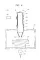
- FIG. 8is a perspective view of another embodiment of a remote plasma generator 300
- FIG. 9is a cross-sectional view of the substrate processing apparatus 900 including the remote plasma generator 300 and a process chamber 200 .
- the process chamber of FIG. 9may have the same configuration as the process chamber 200 of FIG. 2 , except for portions of the remote plasma generator 100 .
- the remote plasma generator 300includes a body unit 310 , a driver electrode 320 , a ground electrode 321 , a protection member 350 , an adhesive member 340 , and a cooling channel 370 .
- the driver electrode 320may be fixed to the body unit 310 . In FIG. 8 , the driver electrode 320 surrounds the body unit 310 . In one embodiment, the driver electrode 320 may include a plurality of electrodes spaced apart from one another on a side surface of the body unit 310 .
- the driver electrode 320may be electrically connected to a power source unit 380 and may receive an alternating current (AC) voltage for generating plasma from the power source unit 380 .
- the AC voltage applied to the driver electrode 320may be a voltage of several hundred V or higher and may have a frequency of several tens of kHz to several tens of MHz.
- the ground electrode 321may be fixed to the body unit 310 and interposed between the driver electrode 320 and the plasma exhaust port 313 . In FIG. 8 , the ground electrode 321 surrounds the body unit 310 . In one embodiment, the ground electrode 321 may include a plurality of electrodes spaced apart from one another on a side surface of the body unit 310 .
- the driver electrode 320When the driver electrode 320 receives an AC voltage from the power source unit 380 , an electric field is formed in the body unit 310 based on a difference in electric potential between the driver electrode 320 and the ground electrode 321 . Thus, plasma discharge may occur due to the discharge gas supplied through gas injection port 312 .
- the protection member 350may be on an inner side of the body unit 310 to prevent the body unit 310 from being damaged due to plasma.
- the protection member 350may include a coating layer of a plasma corrosion resistance material on an inner side of the body unit 350 .
- the protection member 350may be manufactured in bulk using a plasma corrosion resistance material and may be mounted on the inner side of the body unit 310 .
- the protection member 350may include a coating layer of yttrium oxide (Y 2 O 3 ) or may be manufactured in bulk using yttrium oxide.
- the protection member 350may be formed by using, for example, a metal material (e.g., aluminum (Al), titanium (Ti), palladium (Pa), zirconium (Zr), hafnium (Hf), niobium (Nb), or yttrium (Y)), an alloy of the metal material, a ceramic material, or a combination thereof.
- a metal materiale.g., aluminum (Al), titanium (Ti), palladium (Pa), zirconium (Zr), hafnium (Hf), niobium (Nb), or yttrium (Y)
- Alaluminum
- Tititanium
- Papalladium
- Zrzirconium
- Hfhafnium
- Nbniobium
- Yyttrium
- the adhesive member 340may be between the protection member 350 and the body unit 310 to improve mechanical connection therebetween.
- the adhesive member 340may be, for example, a silicone adhesive.
- the adhesive member 340may function as a heating medium.
- the protection member 350is formed of a material having a low thermal shock resistance, the adhesive member 340 may effectively prevent the protection member 350 from being thermally deformed and broken.
- High-temperature heat generated in the body unit 310may be externally transmitted through the protection member 350 , the adhesive member 340 , and the body unit 310 and cooled off by the cooling channel 370 inside or outside the body unit 310 .
- the remote plasma generator 300may include the cooling channel 370 .
- the cooling channel 370may include a single channel or a plurality of channels inside or outside the body unit 310 .
- the cooling channel 370may be, for example, a straight conduit or a spiral conduit.
- a controllermay receive a temperature signal from a sensor for measuring the temperature of the protection member 350 .
- the sensorapplies a control signal to a cooling medium supply unit and a cooling medium recovery unit, in order to control the flow rate of a cooling medium that circulates in the cooling channel 370 .
- FIGS. 10 to 13illustrate embodiments of a plasma inlet prevention structure for preventing the adhesive member 340 from being etched due to plasma.
- FIGS. 10 to 12are enlarged cross-sectional views of embodiments of region C in FIG. 9
- FIG. 13is an enlarged cross-sectional view of an embodiment of region D of FIG. 9 .
- the protection member 350includes a first bent portion 351 and a second bent portion 352 .
- the first bent portion 351extends from an end portion of the protection member 350 in a first direction and covers an end of the adhesive member 340 .
- the second bent portion 352extends from an end portion of the first direction of the first bent portion 351 in a second direction crossing the first direction.
- the protection member 350 including the first bent portion 351 and the second bent portion 352forms a stepped structure that covers the adhesive member 340 . This structure may prevent plasma from flowing into the adhesive member 340 .
- a protection ring 360 ais at an end portion of the protection member 350 and contacts an end of the adhesive member 340 .
- the protection ring 360 aincludes a stepped portion at an outer circumference of the protection ring 360 a and extends in a direction crossing a main surface of the protection ring 360 s .
- the protection member 350 bmay be combined with the protection ring 360 a to form a stepped structure to cover the adhesive member 340 to prevent plasma from flowing into the adhesive member 340 .
- a protection ring 360 bmay be at an end portion of the adhesive member 340 to prevent the adhesive member 340 from being exposed to plasma.
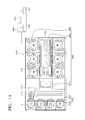
- FIG. 14illustrates an embodiment of a processing system 1000 which includes a substrate processing apparatus.
- the processing system 1000includes an index module 2000 and a process module 3000 .
- the index module 2000receives a substrate from the outside and transfers the substrate to the process module 3000 .
- the process module 3000performs one or more operations on the substrate.
- the index module 2000includes at least one load port 2100 and at least one transfer frame 2200 to facilitate transfer of the substrate.
- a container C including a substratemay be placed in the load port 2100 .
- At least one front opening unified pod (FOUP)may be used as the container C.
- the container Cmay be loaded into the load port 2100 from the outside or unloaded from the load port 2100 to the outside using an overhead transfer (OHT).
- OHToverhead transfer
- the transfer frame 2200transfers the substrate between the container C in the load port 2100 and the process module 3000 .
- the transfer frame 2200may include an index robot 2210 and an index rail 2220 .
- the index robot 2210transfers the substrate while moving on the index rail 2220 .
- the process module 3000performs one or more processes and may include a loadlock chamber 3100 , a transfer chamber 3200 , and a process chamber 4000 .
- the loadlock chamber 3100may include a first port connected to the index module 2000 and a second port connected to the transfer chamber 3200 , and may provide a space in which the substrate temporarily stays.
- the loadlock chamber 3100may have a buffer slot in which the substrate is placed.
- the loadlock chamber 3100may include a plurality of buffer slots formed in a vertical direction. A plurality of substrates may be stacked in the plurality of buffer slots.
- the index robot 2210may withdraw a substrate from the container C and place the substrate in the buffer slot.
- a transfer robot 3210 of the transfer chamber 3200may withdraw the substrate from the buffer slot and transfer the substrate to the process chamber 4000 .
- a pressure control systemmay be connected to the loadlock chamber 3100 .
- the pressure control systemmay control a pressure and facilitate the transfer of the substrate.
- the transfer chamber 3200transfers the substrate between the loadlock chamber 3100 and the process chamber 4000 , which are disposed around the transfer chamber 3200 .
- the transfer chamber 3200may include the transfer robot 3210 and a transfer rail 3220 .
- the transfer robot 3210may transfer the substrate while moving on the transfer rail 3220 .
- the process chamber 4000may be a substrate processing apparatus according to one or more embodiments described herein and may be disposed around the transfer chamber 3200 .
- the process chamber 4000may receive a substrate from the transfer chamber 3200 and process the substrate.
- the process module 3000may include a plurality of process chambers 4000 .
- the process chambers 4000may be, for example, in a row at one side of the transfer chamber 3200 and/or another side thereof along a lengthwise direction of the transfer chamber 3200 .
- the process chambers 4000may be stacked in a vertical direction.
- the process chambers 400may have a different arrangement taking into consideration, for example, factors, such as a footprint or process efficiency.
- a system controller 5000may be connected to the processing system 1000 .
- the system controller 5000may directly control the process chamber 4000 or control a computer (or controller) related to the process chamber 400 to control operations of the process system 1000 .
- the system controller 5000may collect data or perform a feedback operation to optimize performance of the processing system 1000 .
- the system controller 5000may include a central processing unit (CPU) 5100 , a memory 5200 , and a support circuit 5300 .
- the CPUS 100may be one of general-use computers used for industrial setting.
- the support circuit 5300may be normally connected to the CPU 5100 and include a cache, a clock circuit, an input/output circuit, and a power supply.
Landscapes
- Physics & Mathematics (AREA)
- Engineering & Computer Science (AREA)
- Plasma & Fusion (AREA)
- Chemical & Material Sciences (AREA)
- Analytical Chemistry (AREA)
- Spectroscopy & Molecular Physics (AREA)
- Electromagnetism (AREA)
- Fluid Mechanics (AREA)
- Plasma Technology (AREA)
- Drying Of Semiconductors (AREA)
Abstract
Description
- Korean Patent Application No. 10-2015-0052460, filed on Apr. 14, 2015, and entitled, “Remote Plasma Generator Capable of Reducing Particles by Using Ceramic,” is incorporated by reference herein in its entirety.
- 1. Field
- One or more embodiments described herein relate to a remote plasma generator using ceramic.
- 2. Description of the Related Art
- A remote plasma generator generates plasma outside of a process chamber for use by a semiconductor process performed in the process chamber. Attempts have been made to improve the corrosion resistance, abrasion resistance, and heat resistance of the generator using an aluminum anodizing coating layer. However, particles may be produced by the aluminum anodizing coating layer during the process. The particles may contaminate the process and cause the remote plasma generator to malfunction.
- In accordance with one or more embodiments, a remote plasma generator includes a body including a gas injection port, a plasma exhaust port, and a plasma generation pipe through which discharge gas or plasma flow; a driver, coupled to the body, to generate a magnetic field and plasma in the body; and a protection tube, at an inner side of the plasma generation pipe, to protect the plasma generation pipe from plasma. The generator may include a protection layer at a portion of an inner side of the body except for the inner side of the plasma generation pipe. The protection layer may include a coating layer having plasma corrosion resistance. The protection tube may include yttrium oxide.
- A tolerance between the protection tube and the plasma generation pipe may be about 0.1 mm to about 10 mm. The generator may include an adhesive layer between the plasma generation pipe and protection tube. The protection tube may include a first bent portion extending from at least one of two end portions of the protection tube in a first direction and covering an end of the adhesive layer; and a second bent portion extending in a second direction crossing the first direction of the first bent portion.
- The protection tube may include a first bent portion extending from at least one of two end portions of the protection tube in a first direction and covering an end of the adhesive layer; and a protection ring at an end of the first bent portion. The generator may include a protection ring at least one of two end portions of the protection tube and covering an end of the adhesive layer, and the protection ring may have an outer circumference with a stepped portion and extends in a direction crossing a main surface thereof. The adhesive layer may include a silicone adhesive.
- The generator may include a cooling channel formed in the body to circulate a cooling medium, and the cooling channel may have a first side connected to a cooling medium supply source and a second side connected to a cooling medium recovery device. The generator may include a temperature sensor to measure a temperature of the protection tube; and a controller to receive a temperature signal from the temperature sensor and apply control signals to the cooling medium supply source and cooling medium recovery device.
- In accordance with one or more other embodiments, a remote plasma generator includes a body including a gas injection port and a plasma exhaust port; a driver electrode, fixed to the body, to receive an alternating-current (AC) voltage and to generate plasma in the body; a ground electrode fixed to the body and interposed between the driver electrode and the plasma exhaust port; and a protection layer to protect an inners side of the body from plasma. The protection layer may include yttrium oxide. The generator may include an adhesive layer between the body and the protection layer.
- In accordance with one or more other embodiments, an apparatus for a plasma generator includes a pipe to transfer gas or plasma; and a protection layer on an inner surface the pipe, wherein the protection layer separates the inner surface of the pipe from the gas or plasma and includes a first portion extending in a first direction substantially parallel to the inner surface of the pipe and a second portion crossing the first direction, the second portion overlapping an end of the pipe and an end of a body adjacent to the end of the pipe, the protection layer including a material resistant to corrosion from the gas or plasma. The material may include yttrium oxide.
- The apparatus may include a third portion contacting the second portion of the protection layer, wherein the third portion extends from the end of the second portion of the protection layer in the first direction. The third portion may be integrally formed with the second portion. The third portion may be a ring contacting the second portion of the protection layer.
- Features will become apparent to those of skill in the art by describing in detail exemplary embodiments with reference to the attached drawings in which:
FIG. 1 illustrates an embodiment of a remote plasma generator;FIG. 2 illustrates an embodiment of a substrate processing apparatus;FIGS. 3 to 5 illustrate embodiments of region A inFIG. 2 ;FIG. 6 illustrates an embodiment of region B inFIG. 2 ;FIG. 7 illustrates another embodiment of region B;FIG. 8 illustrates another embodiment of a remote plasma generator;FIG. 9 illustrates another embodiment of a substrate processing apparatus;FIGS. 10 to 12 illustrate embodiments of region C inFIG. 9 ;FIG. 13 illustrates an embodiment of region D inFIG. 9 ; andFIG. 14 illustrates an embodiment of a processing system.- Example embodiments are described hereinafter with reference to the drawings; however, they may be embodied in different forms and should not be construed as limited to the embodiments set forth herein. Rather, these embodiments are provided so that this disclosure will be thorough and complete, and will fully convey exemplary implementations to those skilled in the art. The embodiments may be combined to form additional embodiments.
- It will also be understood that when a layer or element is referred to as being “on” another layer or substrate, it can be directly on the other layer or substrate, or intervening layers may also be present. Further, it will be understood that when a layer is referred to as being “under” another layer, it can be directly under, and one or more intervening layers may also be present. In addition, it will also be understood that when a layer is referred to as being “between” two layers, it can be the only layer between the two layers, or one or more intervening layers may also be present. Like reference numerals refer to like elements throughout.
- When an element is referred to as being “connected” or “coupled” to another element, it can be directly connected or coupled to the another element or be indirectly connected or coupled to the another element with one or more intervening elements interposed therebetween. In addition, when an element is referred to as “including” a component, this indicates that the element may further include another component instead of excluding another component unless there is different disclosure.
FIG. 1 illustrates an embodiment of aremote plasma generator 100, andFIG. 2 is a cross-sectional view of an embodiment of asubstrate processing apparatus 800 including theremote plasma generator 100 and aprocess chamber 200.- Referring to
FIGS. 1 and 2 , theremote plasma generator 100 includes abody unit 110, adriver unit 120, aprotection tube 130, anadhesive member 140, and aprotection member 150. - The
body unit 110 has one side that includes agas injection port 112 and another side that includes aplasma exhaust port 113. Thegas injection port 112 receives discharge gas from a gas supply unit, and theplasma exhaust port 113 exhausts plasma to theprocess chamber 200. Thebody unit 110 may include aplasma generation pipe 111 between thegas injection port 112 and theplasma exhaust port 113. In one embodiment, theplasma generation pipe 111 refers to a portion of thebody unit 110 that includes a path through which the discharge gas or plasma is transmitted. A vertically cut section of the path may have one of various sectional shapes, e.g., circular shape, square shape, or elliptical shape. Furthermore, thebody unit 110 may include an ignition electrode for causing ignition during plasma discharge. - The
driver unit 120 may be mounted on thebody unit 110 and may include a magnetic core formed of a ferrite material, iron (Fe), or air. In one embodiment, thedriver unit 120 may be a magnetic core fixed to theplasma generation pipe 111. Thedriver unit 120 may include aprimary coil 121 and electrically connected to apower source unit 180 through aradio frequency cable 181. Thebody unit 110 may receive the discharge gas from the gas supply unit and may receive a radio frequency signal from thepower source unit 180. When current is supplied to theprimary coil 121, induced electromagnetic force is transmitted to the inside of thebody unit 110. The discharge gas is excited by an induced electric field in thebody unit 110 to generate plasma. - The discharge gas injected into the
body unit 110 may be an inert gas (e.g., helium (He), neon (Ne), argon (Ar), and nitrogen (N2)) or a mixture of an inert gas and clean dry air. - A reactive gas or process gas may be added to the discharge gas. The reactive gas or process gas may be selected, for example, to perform one or more functions, e.g., cleaning, etching, atomic layer deposition (ALD), surface processing, or material decomposition. The reactive gas or process gas may include, for example, SF6, CH4, CF4, O2, or NF3and may include a liquid precursor such as but not limited to tetra-ethyl-ortho-silicate (TEOS), tetrakis((ethylmethylamino)zirconium)), trimethyl aluminum, or hexamethyldisiloxane.
- The
protection tube 130 may prevent an inner wall of theplasma generation pipe 111 from being etched due to plasma. Theprotection tube 130 may be manufactured in bulk by using a plasma corrosion resistance material, and added on an inner side of theplasma generation pipe 111 and mounted in theplasma generation pipe 111. - Although a coating layer having plasma corrosion resistance may be formed on the inner side of the
plasma generation pipe 111, it may be difficult to effectively perform a coating operation on the inner side of theplasma generation pipe 111 due to a shape of theplasma generation pipe 111 and a size of a coating nozzle. Thus, it may be effective to manufacture theprotection tube 130 in bulk by using a plasma corrosion resistance material. - The
protection tube 130 for protecting theremote plasma generator 100 may be formed by selecting a plasma corrosion resistance material. The plasma corrosion resistance material may include, for example, a metal material (e.g., aluminum (Al), titanium (Ti), palladium (Pa), zirconium (Zr), hafnium (Hf), niobium (Nb), or yttrium (Y)), an alloy of the metal material, a ceramic material, or a combination thereof. - In one embodiment, the
protection tube 130 may be manufactured using yttrium oxide (Y2O3) that is a ceramic material. Although an anodizing coating layer has been used to prevent damage to the inside of a semiconductor device, particles generated when the anodizing coating layer is etched due to plasma may act as a contamination source in the semiconductor device and cause malfunctions in the semiconductor device. - In contrast, since yttrium oxide has a higher plasma corrosion resistance than the anodizing coating layer, yttrium oxide may prevent the inside of the
body unit 110 from being exposed to plasma and damaged, and may also reduce generation of particles due to the etching of a wall surface of thebody unit 110 or a coating layer for protecting thebody unit 110. Therefore, yttrium oxide may reduce defects in the semiconductor device due to the particles. - In addition, when the
protection tube 130 is manufactured in bulk using yttrium oxide as a material, theprotection tube 130 may have a higher plasma corrosion resistance than when a yttrium oxide coating layer is used. However, when theprotection tube 130 is manufactured in bulk using yttrium oxide, theprotection tube 130 may have weak mechanical properties and may be deformed or damaged due to stress or heat. Thus, a tolerance between theplasma generation pipe 111 and theprotection tube 130 may have to be managed or theadhesive member 140 may be interposed between theplasma generation pipe 111 andprotection tube 130. - In an embodiment, the
protection tube 130 and theplasma generation pipe 111 may be mounted with a tolerance of about 0.1 mm to about 10 mm therebetween, without using theadhesive member 140. Where theprotection tube 130 is manufactured in bulk using a material such as yttrium oxide, which has weak mechanical properties and is easily deformed or damaged due to stress or heat, theprotection tube 130 may be thermally deformed and broken when the tolerance is excessively small. Also, heat may not be efficiently transmitted when the tolerance is excessively large. Thus, an appropriate tolerance may be provided. - In one embodiment, the
protection tube 130 may have a thickness of about 1.7 mm or less. When theprotection tube 130 is manufactured using a material having a low thermal shock resistance, the difference in temperature inside and outside of theprotection tube 130 may increase when theprotection tube 130 has a large thickness, e.g., above a predetermined value. Thus, theprotection tube 130 may be damaged. - In one embodiment, the
protection member 150 formed of a plasma corrosion resistance material may be formed on the remaining portion of the inner side of thebody unit 110, except for the inner side of theplasma generation pipe 111 on which theprotection tube 130 is mounted. Theprotection member 150 may include a coating layer formed of a plasma corrosion resistance material or manufactured in bulk using a plasma corrosion resistance material. Also, in an embodiment, an ignition electrode may be formed in an upper portion of thebody unit 110. Because a lot of particles are generated around the ignition electrode, a cover unit, including a member formed of a plasma corrosion resistance material, may surround the ignition electrode in order to reduce the generation of the particles. - The coating layer inside the
body unit 110 may be formed of a plasma corrosion resistance material using, for example, a plasma spray coating technique, a sputtering process, a beam evaporation process, or a chemical vapor deposition process. - When the
protection member 150 is manufactured in bulk using a plasma corrosion resistance material, theprotection member 150 may be added on the inner side of thebody unit 110 and mounted on thebody unit 110. Based on the shape of the inner side of thebody unit 110, theprotection member 150 may be manufactured in bulk on a portion that is hard to coat because of the size of the coating nozzle. Thus, theprotection member 150 may be mounted on the portion that is hard to coat and effectively protect thebody unit 110. - The
adhesive member 140 may be provided between theprotection tube 130 and theplasma generation pipe 111 to improve mechanical connection therebetween. Theadhesive member 140 may be, for example, a silicone adhesive. Theadhesive member 140 may function as a heating medium. When theprotection tube 130 is formed of a material having a low thermal shock resistance, theadhesive member 140 may effectively prevent theprotection tube 130 from being thermally deformed and broken. High-temperature heat generated in thebody unit 110 may be externally transmitted through theprotection tube 130, theadhesive member 140, and thebody unit 110 and cooled off by the coolingchannel 170 disposed inside or outside thebody unit 110. FIGS. 3 to 5 are enlarged cross-sectional views of various embodiments of region A inFIG. 2 , which corresponds to a plasma inlet prevention structure for preventing theadhesive member 140 from being etched due to plasma.- Referring to
FIG. 3 , theprotection tube 130 may include a firstbent portion 131 and a secondbent portion 132 to prevent plasma from being supplied to and damaging theadhesive member 140. The firstbent portion 131 extends from at least one of two end portions of theprotection tube 130 in a first direction and may cover an end of theadhesive member 140. The secondbent portion 132 extends from an end portion of the firstbent portion 131 in a second direction crossing the first direction. Theprotection tube 130 including the firstbent portion 131 and the secondbent portion 132, therefore, forms a stepped structure in at least one of the two end portions thereof and covers theadhesive member 140. As a result, plasma may be prevented from flowing into and damaging theadhesive member 140. - Referring to
FIG. 4 , plasma may be prevented from flowing into theadhesive member 140 using aprotection ring 160. Theprotection ring 160 may be manufactured, for example, from a ceramic material or yttrium oxide (Y2O3). In one embodiment, theprotection ring 160 may be formed of a plasma corrosion resistance material as described above. Theprotection tube 130amay include a firstbent portion 131awhich extends from at least one of two end portions of theprotection tube 130ain a direction to cover an end of theadhesive member 140. Theprotection ring 160 may be disposed in an end portion of the firstbent portion 131a. Theprotection tube 130amay be combined with theprotection ring 160 to form a stepped structure to prevent plasma from flowing into theadhesive member 140. - Referring to
FIG. 5 , aprotection ring 160amay be disposed in at least one of two end portions of theprotection tube 130b. Theprotection ring 160amay include a stepped portion formed at an outer circumference of theprotection ring 160aand extending in a direction perpendicular to a main surface of theprotection ring 160a. Theprotection ring 160amay cover an end of theadhesive member 140. Theprotection tube 130bmay be combined with theprotection ring 160ato form a stepped structure to prevent plasma from flowing into theadhesive member 140. FIGS. 6 and 7 are enlarged cross-sectional views of embodiments of region B inFIG. 2 , which corresponds to a cooling channel to cool a remote plasma generator.FIG. 6 illustrates a case in which thebody unit 110 includes the coolingchannel 170 between theplasma generation pipe 111 and thedriver unit 120. While circulating through the coolingchannel 170, a cooling medium may cool off thebody unit 110 and theprotection tube 130 and thus may prevent thermal deformation of thebody unit 110 and theprotection tube 130 from high temperatures. The coolingchannel 170 may have one side connected to a coolingmedium supply unit 171 and another side connected to a coolingmedium recovery unit 172. The coolingchannel 170 may include a single channel or a plurality of channels, and may be configured to circulate around theplasma generation pipe 111. Thus, the coolingchannel 170 may be a conduit formed through theplasma generation pipe 111. T cross-section of thecooling channel 170 may not serve as a conduit in another embodiment.- The cooling
medium supply unit 171 and the coolingmedium recovery unit 172 may be connected to acontroller 174. Thecontroller 174 may receive a temperature signal from atemperature sensor 173 that measures the temperature of theprotection tube 130. Thecontroller 170 may then apply control signals to the coolingmedium supply unit 171 and the coolingmedium recovery unit 172 and control a flow rate of a cooling medium, which circulates in coolingchannel 170, in response to control signals. - Referring to
FIG. 7 , the coolingchannel 170 may be, for example, a spiral-type channel inside theplasma generation pipe 111. This structure may increase the area of heat exchange to thereby improve transmission of heat. - Referring back to
FIG. 2 , thesubstrate processing apparatus 800 includes theremote plasma generator 100 and theprocess chamber 200. Theprocess chamber 200 receives plasma through theplasma exhaust port 113 of theremote plasma generator 100. Asubstrate support 210 for supporting asubstrate 220 to be processed may be provided in theprocess chamber 200 and electrically connected to abias power source 230 through animpedance matching device 231. At least onebias power source 230 may be electrically connected to thesubstrate support 210 through theimpedance matching device 231. Thesubstrate processing apparatus 900 may be used in various processes, e.g., a cleaning process, ALD process, surface processing process, or etching process. FIG. 8 is a perspective view of another embodiment of aremote plasma generator 300, andFIG. 9 is a cross-sectional view of thesubstrate processing apparatus 900 including theremote plasma generator 300 and aprocess chamber 200. The process chamber ofFIG. 9 may have the same configuration as theprocess chamber 200 ofFIG. 2 , except for portions of theremote plasma generator 100.- Referring to
FIGS. 8 and 9 , theremote plasma generator 300 includes abody unit 310, adriver electrode 320, aground electrode 321, aprotection member 350, anadhesive member 340, and acooling channel 370. - The
body unit 310 has one side that includes agas injection port 312 and another side that includes aplasma exhaust port 313. Thegas injection port 312 may receive discharge gas from a gas supply unit. Aplasma exhaust port 313 may exhaust plasma to theprocess chamber 200. InFIG. 8 , thebody unit 310 has a cylindrical shape. In another embodiment, thebody unit 310 may have another shape, e.g., a square shape or an elliptical shape. Also, thebody unit 310 may include an ignition electrode for causing ignition during plasma discharge. - The
driver electrode 320 may be fixed to thebody unit 310. InFIG. 8 , thedriver electrode 320 surrounds thebody unit 310. In one embodiment, thedriver electrode 320 may include a plurality of electrodes spaced apart from one another on a side surface of thebody unit 310. Thedriver electrode 320 may be electrically connected to apower source unit 380 and may receive an alternating current (AC) voltage for generating plasma from thepower source unit 380. For example, the AC voltage applied to thedriver electrode 320 may be a voltage of several hundred V or higher and may have a frequency of several tens of kHz to several tens of MHz. - The
ground electrode 321 may be fixed to thebody unit 310 and interposed between thedriver electrode 320 and theplasma exhaust port 313. InFIG. 8 , theground electrode 321 surrounds thebody unit 310. In one embodiment, theground electrode 321 may include a plurality of electrodes spaced apart from one another on a side surface of thebody unit 310. - When the
driver electrode 320 receives an AC voltage from thepower source unit 380, an electric field is formed in thebody unit 310 based on a difference in electric potential between thedriver electrode 320 and theground electrode 321. Thus, plasma discharge may occur due to the discharge gas supplied throughgas injection port 312. - The
protection member 350 may be on an inner side of thebody unit 310 to prevent thebody unit 310 from being damaged due to plasma. Theprotection member 350 may include a coating layer of a plasma corrosion resistance material on an inner side of thebody unit 350. In another embodiment, theprotection member 350 may be manufactured in bulk using a plasma corrosion resistance material and may be mounted on the inner side of thebody unit 310. In one embodiment, theprotection member 350 may include a coating layer of yttrium oxide (Y2O3) or may be manufactured in bulk using yttrium oxide. In addition to yttrium oxide, theprotection member 350 may be formed by using, for example, a metal material (e.g., aluminum (Al), titanium (Ti), palladium (Pa), zirconium (Zr), hafnium (Hf), niobium (Nb), or yttrium (Y)), an alloy of the metal material, a ceramic material, or a combination thereof. - The
adhesive member 340 may be between theprotection member 350 and thebody unit 310 to improve mechanical connection therebetween. Theadhesive member 340 may be, for example, a silicone adhesive. Theadhesive member 340 may function as a heating medium. When theprotection member 350 is formed of a material having a low thermal shock resistance, theadhesive member 340 may effectively prevent theprotection member 350 from being thermally deformed and broken. High-temperature heat generated in thebody unit 310 may be externally transmitted through theprotection member 350, theadhesive member 340, and thebody unit 310 and cooled off by the coolingchannel 370 inside or outside thebody unit 310. - The
remote plasma generator 300 may include thecooling channel 370. The coolingchannel 370 may include a single channel or a plurality of channels inside or outside thebody unit 310. The coolingchannel 370 may be, for example, a straight conduit or a spiral conduit. As described above with reference toFIGS. 6 and 7 , a controller may receive a temperature signal from a sensor for measuring the temperature of theprotection member 350. The sensor applies a control signal to a cooling medium supply unit and a cooling medium recovery unit, in order to control the flow rate of a cooling medium that circulates in thecooling channel 370. FIGS. 10 to 13 illustrate embodiments of a plasma inlet prevention structure for preventing theadhesive member 340 from being etched due to plasma.FIGS. 10 to 12 are enlarged cross-sectional views of embodiments of region C inFIG. 9 , andFIG. 13 is an enlarged cross-sectional view of an embodiment of region D ofFIG. 9 .- Referring to
FIG. 10 , to prevent plasma from flowing into theadhesive member 340, theprotection member 350 includes a firstbent portion 351 and a secondbent portion 352. The firstbent portion 351 extends from an end portion of theprotection member 350 in a first direction and covers an end of theadhesive member 340. The secondbent portion 352 extends from an end portion of the first direction of the firstbent portion 351 in a second direction crossing the first direction. Theprotection member 350 including the firstbent portion 351 and the secondbent portion 352 forms a stepped structure that covers theadhesive member 340. This structure may prevent plasma from flowing into theadhesive member 340. - Referring to
FIG. 11 , plasma may be prevented from flowing into theadhesive member 340 using aprotection ring 360. Aprotection member 350aincludes a firstbent portion 351athat extends from an end portion of theprotection member 350ain a direction and covers an end of theadhesive member 340. Theprotection ring 360 may be at an end portion of the firstbent portion 351a. Theprotection member 350 may be combined with theprotection ring 360 to form a stepped structure that covers theadhesive member 340. Thus, plasma may be prevented from flowing into theadhesive member 340. - Referring to
FIG. 12 , aprotection ring 360ais at an end portion of theprotection member 350 and contacts an end of theadhesive member 340. Theprotection ring 360aincludes a stepped portion at an outer circumference of theprotection ring 360aand extends in a direction crossing a main surface of the protection ring360s. Theprotection member 350bmay be combined with theprotection ring 360ato form a stepped structure to cover theadhesive member 340 to prevent plasma from flowing into theadhesive member 340. - Referring to
FIG. 13 , in a portion from which plasma is exhausted, aprotection ring 360bmay be at an end portion of theadhesive member 340 to prevent theadhesive member 340 from being exposed to plasma. FIG. 14 illustrates an embodiment of aprocessing system 1000 which includes a substrate processing apparatus. Referring toFIG. 14 , theprocessing system 1000 includes anindex module 2000 and aprocess module 3000. Theindex module 2000 receives a substrate from the outside and transfers the substrate to theprocess module 3000. Theprocess module 3000 performs one or more operations on the substrate.- The
index module 2000 includes at least oneload port 2100 and at least onetransfer frame 2200 to facilitate transfer of the substrate. A container C including a substrate may be placed in theload port 2100. At least one front opening unified pod (FOUP) may be used as the container C. The container C may be loaded into theload port 2100 from the outside or unloaded from theload port 2100 to the outside using an overhead transfer (OHT). - The
transfer frame 2200 transfers the substrate between the container C in theload port 2100 and theprocess module 3000. Thetransfer frame 2200 may include anindex robot 2210 and anindex rail 2220. Theindex robot 2210 transfers the substrate while moving on theindex rail 2220. - The
process module 3000 performs one or more processes and may include aloadlock chamber 3100, atransfer chamber 3200, and aprocess chamber 4000. Theloadlock chamber 3100 may include a first port connected to theindex module 2000 and a second port connected to thetransfer chamber 3200, and may provide a space in which the substrate temporarily stays. Theloadlock chamber 3100 may have a buffer slot in which the substrate is placed. Theloadlock chamber 3100 may include a plurality of buffer slots formed in a vertical direction. A plurality of substrates may be stacked in the plurality of buffer slots. Theindex robot 2210 may withdraw a substrate from the container C and place the substrate in the buffer slot. - A
transfer robot 3210 of thetransfer chamber 3200 may withdraw the substrate from the buffer slot and transfer the substrate to theprocess chamber 4000. A pressure control system may be connected to theloadlock chamber 3100. Thus, when theloadlock chamber 3100 receives a substrate from theindex module 2000 or transfers the substrate to theprocess module 3000, the pressure control system may control a pressure and facilitate the transfer of the substrate. - The
transfer chamber 3200 transfers the substrate between theloadlock chamber 3100 and theprocess chamber 4000, which are disposed around thetransfer chamber 3200. Thetransfer chamber 3200 may include thetransfer robot 3210 and atransfer rail 3220. Thetransfer robot 3210 may transfer the substrate while moving on thetransfer rail 3220. - The
process chamber 4000 may be a substrate processing apparatus according to one or more embodiments described herein and may be disposed around thetransfer chamber 3200. Theprocess chamber 4000 may receive a substrate from thetransfer chamber 3200 and process the substrate. - The
process module 3000 may include a plurality ofprocess chambers 4000. Theprocess chambers 4000 may be, for example, in a row at one side of thetransfer chamber 3200 and/or another side thereof along a lengthwise direction of thetransfer chamber 3200. Also, theprocess chambers 4000 may be stacked in a vertical direction. In another embodiment, the process chambers400 may have a different arrangement taking into consideration, for example, factors, such as a footprint or process efficiency. - A
system controller 5000 may be connected to theprocessing system 1000. Thesystem controller 5000 may directly control theprocess chamber 4000 or control a computer (or controller) related to the process chamber400 to control operations of theprocess system 1000. Thesystem controller 5000 may collect data or perform a feedback operation to optimize performance of theprocessing system 1000. - The
system controller 5000 may include a central processing unit (CPU)5100, amemory 5200, and asupport circuit 5300. TheCPUS 100 may be one of general-use computers used for industrial setting. Thesupport circuit 5300 may be normally connected to theCPU 5100 and include a cache, a clock circuit, an input/output circuit, and a power supply. - Example embodiments have been disclosed herein, and although specific terms are employed, they are used and are to be interpreted in a generic and descriptive sense only and not for purpose of limitation. In some instances, as would be apparent to one of skill in the art as of the filing of the present application, features, characteristics, and/or elements described in connection with a particular embodiment may be used singly or in combination with features, characteristics, and/or elements described in connection with other embodiments unless otherwise indicated. Accordingly, it will be understood by those of skill in the art that various changes in form and details may be made without departing from the spirit and scope of the invention as set forth in the following claims.
Claims (20)
Applications Claiming Priority (2)
| Application Number | Priority Date | Filing Date | Title |
|---|---|---|---|
| KR10-2015-0052460 | 2015-04-14 | ||
| KR1020150052460AKR102376982B1 (en) | 2015-04-14 | 2015-04-14 | Remote plasma generator for reducing particles by using ceramic |
Publications (2)
| Publication Number | Publication Date |
|---|---|
| US20160307739A1true US20160307739A1 (en) | 2016-10-20 |
| US9773645B2 US9773645B2 (en) | 2017-09-26 |
Family
ID=57129215
Family Applications (1)
| Application Number | Title | Priority Date | Filing Date |
|---|---|---|---|
| US15/010,151ActiveUS9773645B2 (en) | 2015-04-14 | 2016-01-29 | Remote plasma generator using ceramic |
Country Status (2)
| Country | Link |
|---|---|
| US (1) | US9773645B2 (en) |
| KR (1) | KR102376982B1 (en) |
Cited By (305)
| Publication number | Priority date | Publication date | Assignee | Title |
|---|---|---|---|---|
| WO2019241405A1 (en)* | 2018-06-14 | 2019-12-19 | Mks Instruments, Inc. | Radical output monitor for a remote plasma source and method of use |
| CN110612593A (en)* | 2017-05-31 | 2019-12-24 | 应用材料公司 | Remote Plasma Oxidation Chamber |
| US10720331B2 (en) | 2016-11-01 | 2020-07-21 | ASM IP Holdings, B.V. | Methods for forming a transition metal nitride film on a substrate by atomic layer deposition and related semiconductor device structures |
| US10767789B2 (en) | 2018-07-16 | 2020-09-08 | Asm Ip Holding B.V. | Diaphragm valves, valve components, and methods for forming valve components |
| US10784102B2 (en) | 2016-12-22 | 2020-09-22 | Asm Ip Holding B.V. | Method of forming a structure on a substrate |
| US10787741B2 (en) | 2014-08-21 | 2020-09-29 | Asm Ip Holding B.V. | Method and system for in situ formation of gas-phase compounds |
| US10797133B2 (en) | 2018-06-21 | 2020-10-06 | Asm Ip Holding B.V. | Method for depositing a phosphorus doped silicon arsenide film and related semiconductor device structures |
| US10804098B2 (en) | 2009-08-14 | 2020-10-13 | Asm Ip Holding B.V. | Systems and methods for thin-film deposition of metal oxides using excited nitrogen-oxygen species |
| US10818758B2 (en) | 2018-11-16 | 2020-10-27 | Asm Ip Holding B.V. | Methods for forming a metal silicate film on a substrate in a reaction chamber and related semiconductor device structures |
| US10832903B2 (en) | 2011-10-28 | 2020-11-10 | Asm Ip Holding B.V. | Process feed management for semiconductor substrate processing |
| US10829852B2 (en) | 2018-08-16 | 2020-11-10 | Asm Ip Holding B.V. | Gas distribution device for a wafer processing apparatus |
| US10844484B2 (en) | 2017-09-22 | 2020-11-24 | Asm Ip Holding B.V. | Apparatus for dispensing a vapor phase reactant to a reaction chamber and related methods |
| US10847366B2 (en) | 2018-11-16 | 2020-11-24 | Asm Ip Holding B.V. | Methods for depositing a transition metal chalcogenide film on a substrate by a cyclical deposition process |
| US10847371B2 (en) | 2018-03-27 | 2020-11-24 | Asm Ip Holding B.V. | Method of forming an electrode on a substrate and a semiconductor device structure including an electrode |
| US10844486B2 (en) | 2009-04-06 | 2020-11-24 | Asm Ip Holding B.V. | Semiconductor processing reactor and components thereof |
| US10851456B2 (en) | 2016-04-21 | 2020-12-01 | Asm Ip Holding B.V. | Deposition of metal borides |
| US10858737B2 (en) | 2014-07-28 | 2020-12-08 | Asm Ip Holding B.V. | Showerhead assembly and components thereof |
| US10867786B2 (en) | 2018-03-30 | 2020-12-15 | Asm Ip Holding B.V. | Substrate processing method |
| US10867788B2 (en) | 2016-12-28 | 2020-12-15 | Asm Ip Holding B.V. | Method of forming a structure on a substrate |
| US10865475B2 (en) | 2016-04-21 | 2020-12-15 | Asm Ip Holding B.V. | Deposition of metal borides and silicides |
| US10872771B2 (en) | 2018-01-16 | 2020-12-22 | Asm Ip Holding B. V. | Method for depositing a material film on a substrate within a reaction chamber by a cyclical deposition process and related device structures |
| US10886123B2 (en) | 2017-06-02 | 2021-01-05 | Asm Ip Holding B.V. | Methods for forming low temperature semiconductor layers and related semiconductor device structures |
| US10883175B2 (en) | 2018-08-09 | 2021-01-05 | Asm Ip Holding B.V. | Vertical furnace for processing substrates and a liner for use therein |
| US10892156B2 (en) | 2017-05-08 | 2021-01-12 | Asm Ip Holding B.V. | Methods for forming a silicon nitride film on a substrate and related semiconductor device structures |
| US10896820B2 (en) | 2018-02-14 | 2021-01-19 | Asm Ip Holding B.V. | Method for depositing a ruthenium-containing film on a substrate by a cyclical deposition process |
| US10910262B2 (en) | 2017-11-16 | 2021-02-02 | Asm Ip Holding B.V. | Method of selectively depositing a capping layer structure on a semiconductor device structure |
| US10914004B2 (en) | 2018-06-29 | 2021-02-09 | Asm Ip Holding B.V. | Thin-film deposition method and manufacturing method of semiconductor device |
| US10923344B2 (en) | 2017-10-30 | 2021-02-16 | Asm Ip Holding B.V. | Methods for forming a semiconductor structure and related semiconductor structures |
| US10928731B2 (en) | 2017-09-21 | 2021-02-23 | Asm Ip Holding B.V. | Method of sequential infiltration synthesis treatment of infiltrateable material and structures and devices formed using same |
| US10934619B2 (en) | 2016-11-15 | 2021-03-02 | Asm Ip Holding B.V. | Gas supply unit and substrate processing apparatus including the gas supply unit |
| US10943771B2 (en) | 2016-10-26 | 2021-03-09 | Asm Ip Holding B.V. | Methods for thermally calibrating reaction chambers |
| US10941490B2 (en) | 2014-10-07 | 2021-03-09 | Asm Ip Holding B.V. | Multiple temperature range susceptor, assembly, reactor and system including the susceptor, and methods of using the same |
| US10950432B2 (en) | 2017-04-25 | 2021-03-16 | Asm Ip Holding B.V. | Method of depositing thin film and method of manufacturing semiconductor device |
| USD913980S1 (en) | 2018-02-01 | 2021-03-23 | Asm Ip Holding B.V. | Gas supply plate for semiconductor manufacturing apparatus |
| US10975470B2 (en) | 2018-02-23 | 2021-04-13 | Asm Ip Holding B.V. | Apparatus for detecting or monitoring for a chemical precursor in a high temperature environment |
| US11004977B2 (en) | 2017-07-19 | 2021-05-11 | Asm Ip Holding B.V. | Method for depositing a group IV semiconductor and related semiconductor device structures |
| US11001925B2 (en) | 2016-12-19 | 2021-05-11 | Asm Ip Holding B.V. | Substrate processing apparatus |
| US11018002B2 (en) | 2017-07-19 | 2021-05-25 | Asm Ip Holding B.V. | Method for selectively depositing a Group IV semiconductor and related semiconductor device structures |
| US11018047B2 (en) | 2018-01-25 | 2021-05-25 | Asm Ip Holding B.V. | Hybrid lift pin |
| US11015245B2 (en) | 2014-03-19 | 2021-05-25 | Asm Ip Holding B.V. | Gas-phase reactor and system having exhaust plenum and components thereof |
| US11022879B2 (en) | 2017-11-24 | 2021-06-01 | Asm Ip Holding B.V. | Method of forming an enhanced unexposed photoresist layer |
| US11024523B2 (en) | 2018-09-11 | 2021-06-01 | Asm Ip Holding B.V. | Substrate processing apparatus and method |
| US11031242B2 (en) | 2018-11-07 | 2021-06-08 | Asm Ip Holding B.V. | Methods for depositing a boron doped silicon germanium film |
| USD922229S1 (en) | 2019-06-05 | 2021-06-15 | Asm Ip Holding B.V. | Device for controlling a temperature of a gas supply unit |
| US11049751B2 (en) | 2018-09-14 | 2021-06-29 | Asm Ip Holding B.V. | Cassette supply system to store and handle cassettes and processing apparatus equipped therewith |
| US11053591B2 (en) | 2018-08-06 | 2021-07-06 | Asm Ip Holding B.V. | Multi-port gas injection system and reactor system including same |
| US11056567B2 (en) | 2018-05-11 | 2021-07-06 | Asm Ip Holding B.V. | Method of forming a doped metal carbide film on a substrate and related semiconductor device structures |
| US11056344B2 (en) | 2017-08-30 | 2021-07-06 | Asm Ip Holding B.V. | Layer forming method |
| US11069510B2 (en) | 2017-08-30 | 2021-07-20 | Asm Ip Holding B.V. | Substrate processing apparatus |
| US11081345B2 (en) | 2018-02-06 | 2021-08-03 | Asm Ip Holding B.V. | Method of post-deposition treatment for silicon oxide film |
| US11087997B2 (en) | 2018-10-31 | 2021-08-10 | Asm Ip Holding B.V. | Substrate processing apparatus for processing substrates |
| US11088002B2 (en) | 2018-03-29 | 2021-08-10 | Asm Ip Holding B.V. | Substrate rack and a substrate processing system and method |
| US11094546B2 (en) | 2017-10-05 | 2021-08-17 | Asm Ip Holding B.V. | Method for selectively depositing a metallic film on a substrate |
| US11094582B2 (en) | 2016-07-08 | 2021-08-17 | Asm Ip Holding B.V. | Selective deposition method to form air gaps |
| US11101370B2 (en) | 2016-05-02 | 2021-08-24 | Asm Ip Holding B.V. | Method of forming a germanium oxynitride film |
| US11107676B2 (en) | 2016-07-28 | 2021-08-31 | Asm Ip Holding B.V. | Method and apparatus for filling a gap |
| US11114294B2 (en) | 2019-03-08 | 2021-09-07 | Asm Ip Holding B.V. | Structure including SiOC layer and method of forming same |
| US11114283B2 (en) | 2018-03-16 | 2021-09-07 | Asm Ip Holding B.V. | Reactor, system including the reactor, and methods of manufacturing and using same |
| USD930782S1 (en) | 2019-08-22 | 2021-09-14 | Asm Ip Holding B.V. | Gas distributor |
| US11127589B2 (en) | 2019-02-01 | 2021-09-21 | Asm Ip Holding B.V. | Method of topology-selective film formation of silicon oxide |
| US11127617B2 (en) | 2017-11-27 | 2021-09-21 | Asm Ip Holding B.V. | Storage device for storing wafer cassettes for use with a batch furnace |
| USD931978S1 (en) | 2019-06-27 | 2021-09-28 | Asm Ip Holding B.V. | Showerhead vacuum transport |
| US11139308B2 (en) | 2015-12-29 | 2021-10-05 | Asm Ip Holding B.V. | Atomic layer deposition of III-V compounds to form V-NAND devices |
| US11139191B2 (en) | 2017-08-09 | 2021-10-05 | Asm Ip Holding B.V. | Storage apparatus for storing cassettes for substrates and processing apparatus equipped therewith |
| US11158513B2 (en) | 2018-12-13 | 2021-10-26 | Asm Ip Holding B.V. | Methods for forming a rhenium-containing film on a substrate by a cyclical deposition process and related semiconductor device structures |
| US11164955B2 (en) | 2017-07-18 | 2021-11-02 | Asm Ip Holding B.V. | Methods for forming a semiconductor device structure and related semiconductor device structures |
| US11168395B2 (en) | 2018-06-29 | 2021-11-09 | Asm Ip Holding B.V. | Temperature-controlled flange and reactor system including same |
| USD935572S1 (en) | 2019-05-24 | 2021-11-09 | Asm Ip Holding B.V. | Gas channel plate |
| US11171025B2 (en) | 2019-01-22 | 2021-11-09 | Asm Ip Holding B.V. | Substrate processing device |
| US11205585B2 (en) | 2016-07-28 | 2021-12-21 | Asm Ip Holding B.V. | Substrate processing apparatus and method of operating the same |
| US11217444B2 (en) | 2018-11-30 | 2022-01-04 | Asm Ip Holding B.V. | Method for forming an ultraviolet radiation responsive metal oxide-containing film |
| US11222772B2 (en) | 2016-12-14 | 2022-01-11 | Asm Ip Holding B.V. | Substrate processing apparatus |
| USD940837S1 (en) | 2019-08-22 | 2022-01-11 | Asm Ip Holding B.V. | Electrode |
| US11227789B2 (en) | 2019-02-20 | 2022-01-18 | Asm Ip Holding B.V. | Method and apparatus for filling a recess formed within a substrate surface |
| US11227782B2 (en) | 2019-07-31 | 2022-01-18 | Asm Ip Holding B.V. | Vertical batch furnace assembly |
| US11230766B2 (en) | 2018-03-29 | 2022-01-25 | Asm Ip Holding B.V. | Substrate processing apparatus and method |
| US11233133B2 (en) | 2015-10-21 | 2022-01-25 | Asm Ip Holding B.V. | NbMC layers |
| US11232963B2 (en) | 2018-10-03 | 2022-01-25 | Asm Ip Holding B.V. | Substrate processing apparatus and method |
| US11242598B2 (en) | 2015-06-26 | 2022-02-08 | Asm Ip Holding B.V. | Structures including metal carbide material, devices including the structures, and methods of forming same |
| US11251068B2 (en) | 2018-10-19 | 2022-02-15 | Asm Ip Holding B.V. | Substrate processing apparatus and substrate processing method |
| US11251040B2 (en) | 2019-02-20 | 2022-02-15 | Asm Ip Holding B.V. | Cyclical deposition method including treatment step and apparatus for same |
| USD944946S1 (en) | 2019-06-14 | 2022-03-01 | Asm Ip Holding B.V. | Shower plate |
| US11270899B2 (en) | 2018-06-04 | 2022-03-08 | Asm Ip Holding B.V. | Wafer handling chamber with moisture reduction |
| US11274369B2 (en) | 2018-09-11 | 2022-03-15 | Asm Ip Holding B.V. | Thin film deposition method |
| US11282698B2 (en) | 2019-07-19 | 2022-03-22 | Asm Ip Holding B.V. | Method of forming topology-controlled amorphous carbon polymer film |
| US11286562B2 (en) | 2018-06-08 | 2022-03-29 | Asm Ip Holding B.V. | Gas-phase chemical reactor and method of using same |
| US11286558B2 (en) | 2019-08-23 | 2022-03-29 | Asm Ip Holding B.V. | Methods for depositing a molybdenum nitride film on a surface of a substrate by a cyclical deposition process and related semiconductor device structures including a molybdenum nitride film |
| US11289326B2 (en) | 2019-05-07 | 2022-03-29 | Asm Ip Holding B.V. | Method for reforming amorphous carbon polymer film |
| USD947913S1 (en) | 2019-05-17 | 2022-04-05 | Asm Ip Holding B.V. | Susceptor shaft |
| US11295980B2 (en) | 2017-08-30 | 2022-04-05 | Asm Ip Holding B.V. | Methods for depositing a molybdenum metal film over a dielectric surface of a substrate by a cyclical deposition process and related semiconductor device structures |
| USD948463S1 (en) | 2018-10-24 | 2022-04-12 | Asm Ip Holding B.V. | Susceptor for semiconductor substrate supporting apparatus |
| US11306395B2 (en) | 2017-06-28 | 2022-04-19 | Asm Ip Holding B.V. | Methods for depositing a transition metal nitride film on a substrate by atomic layer deposition and related deposition apparatus |
| USD949319S1 (en) | 2019-08-22 | 2022-04-19 | Asm Ip Holding B.V. | Exhaust duct |
| US11315794B2 (en) | 2019-10-21 | 2022-04-26 | Asm Ip Holding B.V. | Apparatus and methods for selectively etching films |
| US11342216B2 (en) | 2019-02-20 | 2022-05-24 | Asm Ip Holding B.V. | Cyclical deposition method and apparatus for filling a recess formed within a substrate surface |
| US11339476B2 (en) | 2019-10-08 | 2022-05-24 | Asm Ip Holding B.V. | Substrate processing device having connection plates, substrate processing method |
| US11345999B2 (en) | 2019-06-06 | 2022-05-31 | Asm Ip Holding B.V. | Method of using a gas-phase reactor system including analyzing exhausted gas |
| US11355338B2 (en) | 2019-05-10 | 2022-06-07 | Asm Ip Holding B.V. | Method of depositing material onto a surface and structure formed according to the method |
| US11361990B2 (en) | 2018-05-28 | 2022-06-14 | Asm Ip Holding B.V. | Substrate processing method and device manufactured by using the same |
| US11374112B2 (en) | 2017-07-19 | 2022-06-28 | Asm Ip Holding B.V. | Method for depositing a group IV semiconductor and related semiconductor device structures |
| US11378337B2 (en) | 2019-03-28 | 2022-07-05 | Asm Ip Holding B.V. | Door opener and substrate processing apparatus provided therewith |
| US11387120B2 (en) | 2017-09-28 | 2022-07-12 | Asm Ip Holding B.V. | Chemical dispensing apparatus and methods for dispensing a chemical to a reaction chamber |
| US11393690B2 (en) | 2018-01-19 | 2022-07-19 | Asm Ip Holding B.V. | Deposition method |
| US11390945B2 (en) | 2019-07-03 | 2022-07-19 | Asm Ip Holding B.V. | Temperature control assembly for substrate processing apparatus and method of using same |
| US11390950B2 (en) | 2017-01-10 | 2022-07-19 | Asm Ip Holding B.V. | Reactor system and method to reduce residue buildup during a film deposition process |
| US11390946B2 (en) | 2019-01-17 | 2022-07-19 | Asm Ip Holding B.V. | Methods of forming a transition metal containing film on a substrate by a cyclical deposition process |
| US11401605B2 (en) | 2019-11-26 | 2022-08-02 | Asm Ip Holding B.V. | Substrate processing apparatus |
| US11410851B2 (en) | 2017-02-15 | 2022-08-09 | Asm Ip Holding B.V. | Methods for forming a metallic film on a substrate by cyclical deposition and related semiconductor device structures |
| US11417545B2 (en) | 2017-08-08 | 2022-08-16 | Asm Ip Holding B.V. | Radiation shield |
| US11414760B2 (en) | 2018-10-08 | 2022-08-16 | Asm Ip Holding B.V. | Substrate support unit, thin film deposition apparatus including the same, and substrate processing apparatus including the same |
| US11424119B2 (en) | 2019-03-08 | 2022-08-23 | Asm Ip Holding B.V. | Method for selective deposition of silicon nitride layer and structure including selectively-deposited silicon nitride layer |
| US11430640B2 (en) | 2019-07-30 | 2022-08-30 | Asm Ip Holding B.V. | Substrate processing apparatus |
| US11430674B2 (en) | 2018-08-22 | 2022-08-30 | Asm Ip Holding B.V. | Sensor array, apparatus for dispensing a vapor phase reactant to a reaction chamber and related methods |
| US11437241B2 (en) | 2020-04-08 | 2022-09-06 | Asm Ip Holding B.V. | Apparatus and methods for selectively etching silicon oxide films |
| US11443926B2 (en) | 2019-07-30 | 2022-09-13 | Asm Ip Holding B.V. | Substrate processing apparatus |
| US11447864B2 (en) | 2019-04-19 | 2022-09-20 | Asm Ip Holding B.V. | Layer forming method and apparatus |
| US11447861B2 (en) | 2016-12-15 | 2022-09-20 | Asm Ip Holding B.V. | Sequential infiltration synthesis apparatus and a method of forming a patterned structure |
| US11453943B2 (en) | 2016-05-25 | 2022-09-27 | Asm Ip Holding B.V. | Method for forming carbon-containing silicon/metal oxide or nitride film by ALD using silicon precursor and hydrocarbon precursor |
| USD965044S1 (en) | 2019-08-19 | 2022-09-27 | Asm Ip Holding B.V. | Susceptor shaft |
| USD965524S1 (en) | 2019-08-19 | 2022-10-04 | Asm Ip Holding B.V. | Susceptor support |
| US11469098B2 (en) | 2018-05-08 | 2022-10-11 | Asm Ip Holding B.V. | Methods for depositing an oxide film on a substrate by a cyclical deposition process and related device structures |
| US11470711B2 (en)* | 2017-05-16 | 2022-10-11 | Fuji Corporation | Plasma generator with connector-cable detector |
| US11476109B2 (en) | 2019-06-11 | 2022-10-18 | Asm Ip Holding B.V. | Method of forming an electronic structure using reforming gas, system for performing the method, and structure formed using the method |
| US11473195B2 (en) | 2018-03-01 | 2022-10-18 | Asm Ip Holding B.V. | Semiconductor processing apparatus and a method for processing a substrate |
| US11482412B2 (en) | 2018-01-19 | 2022-10-25 | Asm Ip Holding B.V. | Method for depositing a gap-fill layer by plasma-assisted deposition |
| US11482533B2 (en) | 2019-02-20 | 2022-10-25 | Asm Ip Holding B.V. | Apparatus and methods for plug fill deposition in 3-D NAND applications |
| US11482418B2 (en) | 2018-02-20 | 2022-10-25 | Asm Ip Holding B.V. | Substrate processing method and apparatus |
| US11488819B2 (en) | 2018-12-04 | 2022-11-01 | Asm Ip Holding B.V. | Method of cleaning substrate processing apparatus |
| US11488854B2 (en) | 2020-03-11 | 2022-11-01 | Asm Ip Holding B.V. | Substrate handling device with adjustable joints |
| US11492703B2 (en) | 2018-06-27 | 2022-11-08 | Asm Ip Holding B.V. | Cyclic deposition methods for forming metal-containing material and films and structures including the metal-containing material |
| US11495459B2 (en) | 2019-09-04 | 2022-11-08 | Asm Ip Holding B.V. | Methods for selective deposition using a sacrificial capping layer |
| US11501956B2 (en) | 2012-10-12 | 2022-11-15 | Asm Ip Holding B.V. | Semiconductor reaction chamber showerhead |
| US11499226B2 (en) | 2018-11-02 | 2022-11-15 | Asm Ip Holding B.V. | Substrate supporting unit and a substrate processing device including the same |
| US11499222B2 (en) | 2018-06-27 | 2022-11-15 | Asm Ip Holding B.V. | Cyclic deposition methods for forming metal-containing material and films and structures including the metal-containing material |
| US11501968B2 (en) | 2019-11-15 | 2022-11-15 | Asm Ip Holding B.V. | Method for providing a semiconductor device with silicon filled gaps |
| US11515188B2 (en) | 2019-05-16 | 2022-11-29 | Asm Ip Holding B.V. | Wafer boat handling device, vertical batch furnace and method |
| US11515187B2 (en) | 2020-05-01 | 2022-11-29 | Asm Ip Holding B.V. | Fast FOUP swapping with a FOUP handler |
| US11521851B2 (en) | 2020-02-03 | 2022-12-06 | Asm Ip Holding B.V. | Method of forming structures including a vanadium or indium layer |
| US11527403B2 (en) | 2019-12-19 | 2022-12-13 | Asm Ip Holding B.V. | Methods for filling a gap feature on a substrate surface and related semiconductor structures |
| US11527400B2 (en) | 2019-08-23 | 2022-12-13 | Asm Ip Holding B.V. | Method for depositing silicon oxide film having improved quality by peald using bis(diethylamino)silane |
| US11530876B2 (en) | 2020-04-24 | 2022-12-20 | Asm Ip Holding B.V. | Vertical batch furnace assembly comprising a cooling gas supply |
| US11530483B2 (en) | 2018-06-21 | 2022-12-20 | Asm Ip Holding B.V. | Substrate processing system |
| US11532757B2 (en) | 2016-10-27 | 2022-12-20 | Asm Ip Holding B.V. | Deposition of charge trapping layers |
| US11551912B2 (en) | 2020-01-20 | 2023-01-10 | Asm Ip Holding B.V. | Method of forming thin film and method of modifying surface of thin film |
| US11551925B2 (en) | 2019-04-01 | 2023-01-10 | Asm Ip Holding B.V. | Method for manufacturing a semiconductor device |
| US11557474B2 (en) | 2019-07-29 | 2023-01-17 | Asm Ip Holding B.V. | Methods for selective deposition utilizing n-type dopants and/or alternative dopants to achieve high dopant incorporation |
| USD975665S1 (en) | 2019-05-17 | 2023-01-17 | Asm Ip Holding B.V. | Susceptor shaft |
| US11562901B2 (en) | 2019-09-25 | 2023-01-24 | Asm Ip Holding B.V. | Substrate processing method |
| US11572620B2 (en) | 2018-11-06 | 2023-02-07 | Asm Ip Holding B.V. | Methods for selectively depositing an amorphous silicon film on a substrate |
| US11581186B2 (en) | 2016-12-15 | 2023-02-14 | Asm Ip Holding B.V. | Sequential infiltration synthesis apparatus |
| US11587814B2 (en) | 2019-07-31 | 2023-02-21 | Asm Ip Holding B.V. | Vertical batch furnace assembly |
| US11587815B2 (en) | 2019-07-31 | 2023-02-21 | Asm Ip Holding B.V. | Vertical batch furnace assembly |
| US11587821B2 (en) | 2017-08-08 | 2023-02-21 | Asm Ip Holding B.V. | Substrate lift mechanism and reactor including same |
| US11594450B2 (en) | 2019-08-22 | 2023-02-28 | Asm Ip Holding B.V. | Method for forming a structure with a hole |
| US11594600B2 (en) | 2019-11-05 | 2023-02-28 | Asm Ip Holding B.V. | Structures with doped semiconductor layers and methods and systems for forming same |
| USD979506S1 (en) | 2019-08-22 | 2023-02-28 | Asm Ip Holding B.V. | Insulator |
| USD980814S1 (en) | 2021-05-11 | 2023-03-14 | Asm Ip Holding B.V. | Gas distributor for substrate processing apparatus |
| USD980813S1 (en) | 2021-05-11 | 2023-03-14 | Asm Ip Holding B.V. | Gas flow control plate for substrate processing apparatus |
| US11605528B2 (en) | 2019-07-09 | 2023-03-14 | Asm Ip Holding B.V. | Plasma device using coaxial waveguide, and substrate treatment method |
| US11610774B2 (en) | 2019-10-02 | 2023-03-21 | Asm Ip Holding B.V. | Methods for forming a topographically selective silicon oxide film by a cyclical plasma-enhanced deposition process |
| US11610775B2 (en) | 2016-07-28 | 2023-03-21 | Asm Ip Holding B.V. | Method and apparatus for filling a gap |
| USD981973S1 (en) | 2021-05-11 | 2023-03-28 | Asm Ip Holding B.V. | Reactor wall for substrate processing apparatus |
| US11615970B2 (en) | 2019-07-17 | 2023-03-28 | Asm Ip Holding B.V. | Radical assist ignition plasma system and method |
| US11626308B2 (en) | 2020-05-13 | 2023-04-11 | Asm Ip Holding B.V. | Laser alignment fixture for a reactor system |
| US11626316B2 (en) | 2019-11-20 | 2023-04-11 | Asm Ip Holding B.V. | Method of depositing carbon-containing material on a surface of a substrate, structure formed using the method, and system for forming the structure |
| US11629407B2 (en) | 2019-02-22 | 2023-04-18 | Asm Ip Holding B.V. | Substrate processing apparatus and method for processing substrates |
| US11629406B2 (en) | 2018-03-09 | 2023-04-18 | Asm Ip Holding B.V. | Semiconductor processing apparatus comprising one or more pyrometers for measuring a temperature of a substrate during transfer of the substrate |
| US11637011B2 (en) | 2019-10-16 | 2023-04-25 | Asm Ip Holding B.V. | Method of topology-selective film formation of silicon oxide |
| US11637014B2 (en) | 2019-10-17 | 2023-04-25 | Asm Ip Holding B.V. | Methods for selective deposition of doped semiconductor material |
| US11639811B2 (en) | 2017-11-27 | 2023-05-02 | Asm Ip Holding B.V. | Apparatus including a clean mini environment |
| US11639548B2 (en) | 2019-08-21 | 2023-05-02 | Asm Ip Holding B.V. | Film-forming material mixed-gas forming device and film forming device |
| US11646205B2 (en) | 2019-10-29 | 2023-05-09 | Asm Ip Holding B.V. | Methods of selectively forming n-type doped material on a surface, systems for selectively forming n-type doped material, and structures formed using same |
| US11643724B2 (en) | 2019-07-18 | 2023-05-09 | Asm Ip Holding B.V. | Method of forming structures using a neutral beam |
| US11646204B2 (en) | 2020-06-24 | 2023-05-09 | Asm Ip Holding B.V. | Method for forming a layer provided with silicon |
| US11646197B2 (en) | 2018-07-03 | 2023-05-09 | Asm Ip Holding B.V. | Method for depositing silicon-free carbon-containing film as gap-fill layer by pulse plasma-assisted deposition |
| US11644758B2 (en) | 2020-07-17 | 2023-05-09 | Asm Ip Holding B.V. | Structures and methods for use in photolithography |
| US11646184B2 (en) | 2019-11-29 | 2023-05-09 | Asm Ip Holding B.V. | Substrate processing apparatus |
| US11649546B2 (en) | 2016-07-08 | 2023-05-16 | Asm Ip Holding B.V. | Organic reactants for atomic layer deposition |
| US11658035B2 (en) | 2020-06-30 | 2023-05-23 | Asm Ip Holding B.V. | Substrate processing method |
| US11658030B2 (en) | 2017-03-29 | 2023-05-23 | Asm Ip Holding B.V. | Method for forming doped metal oxide films on a substrate by cyclical deposition and related semiconductor device structures |
| US11658029B2 (en) | 2018-12-14 | 2023-05-23 | Asm Ip Holding B.V. | Method of forming a device structure using selective deposition of gallium nitride and system for same |
| US11664267B2 (en) | 2019-07-10 | 2023-05-30 | Asm Ip Holding B.V. | Substrate support assembly and substrate processing device including the same |
| US11664245B2 (en) | 2019-07-16 | 2023-05-30 | Asm Ip Holding B.V. | Substrate processing device |
| US11664199B2 (en) | 2018-10-19 | 2023-05-30 | Asm Ip Holding B.V. | Substrate processing apparatus and substrate processing method |
| US11674220B2 (en) | 2020-07-20 | 2023-06-13 | Asm Ip Holding B.V. | Method for depositing molybdenum layers using an underlayer |
| US11676812B2 (en) | 2016-02-19 | 2023-06-13 | Asm Ip Holding B.V. | Method for forming silicon nitride film selectively on top/bottom portions |
| US11680839B2 (en) | 2019-08-05 | 2023-06-20 | Asm Ip Holding B.V. | Liquid level sensor for a chemical source vessel |
| USD990534S1 (en) | 2020-09-11 | 2023-06-27 | Asm Ip Holding B.V. | Weighted lift pin |
| US11685991B2 (en) | 2018-02-14 | 2023-06-27 | Asm Ip Holding B.V. | Method for depositing a ruthenium-containing film on a substrate by a cyclical deposition process |
| USD990441S1 (en) | 2021-09-07 | 2023-06-27 | Asm Ip Holding B.V. | Gas flow control plate |
| US11688603B2 (en) | 2019-07-17 | 2023-06-27 | Asm Ip Holding B.V. | Methods of forming silicon germanium structures |
| CN116390317A (en)* | 2023-04-19 | 2023-07-04 | 江苏神州半导体科技有限公司 | Remote plasma generator |
| US11705333B2 (en) | 2020-05-21 | 2023-07-18 | Asm Ip Holding B.V. | Structures including multiple carbon layers and methods of forming and using same |
| US11718913B2 (en) | 2018-06-04 | 2023-08-08 | Asm Ip Holding B.V. | Gas distribution system and reactor system including same |
| US11725277B2 (en) | 2011-07-20 | 2023-08-15 | Asm Ip Holding B.V. | Pressure transmitter for a semiconductor processing environment |
| US11725280B2 (en) | 2020-08-26 | 2023-08-15 | Asm Ip Holding B.V. | Method for forming metal silicon oxide and metal silicon oxynitride layers |
| US11735422B2 (en) | 2019-10-10 | 2023-08-22 | Asm Ip Holding B.V. | Method of forming a photoresist underlayer and structure including same |
| US11742189B2 (en) | 2015-03-12 | 2023-08-29 | Asm Ip Holding B.V. | Multi-zone reactor, system including the reactor, and method of using the same |
| US11742198B2 (en) | 2019-03-08 | 2023-08-29 | Asm Ip Holding B.V. | Structure including SiOCN layer and method of forming same |
| US11769682B2 (en) | 2017-08-09 | 2023-09-26 | Asm Ip Holding B.V. | Storage apparatus for storing cassettes for substrates and processing apparatus equipped therewith |
| US11767589B2 (en) | 2020-05-29 | 2023-09-26 | Asm Ip Holding B.V. | Substrate processing device |
| US11776846B2 (en) | 2020-02-07 | 2023-10-03 | Asm Ip Holding B.V. | Methods for depositing gap filling fluids and related systems and devices |
| US11781221B2 (en) | 2019-05-07 | 2023-10-10 | Asm Ip Holding B.V. | Chemical source vessel with dip tube |
| US11781243B2 (en) | 2020-02-17 | 2023-10-10 | Asm Ip Holding B.V. | Method for depositing low temperature phosphorous-doped silicon |
| US11802338B2 (en) | 2017-07-26 | 2023-10-31 | Asm Ip Holding B.V. | Chemical treatment, deposition and/or infiltration apparatus and method for using the same |
| US11804364B2 (en) | 2020-05-19 | 2023-10-31 | Asm Ip Holding B.V. | Substrate processing apparatus |
| US11810788B2 (en) | 2016-11-01 | 2023-11-07 | Asm Ip Holding B.V. | Methods for forming a transition metal niobium nitride film on a substrate by atomic layer deposition and related semiconductor device structures |
| US11814747B2 (en) | 2019-04-24 | 2023-11-14 | Asm Ip Holding B.V. | Gas-phase reactor system-with a reaction chamber, a solid precursor source vessel, a gas distribution system, and a flange assembly |
| US11823876B2 (en) | 2019-09-05 | 2023-11-21 | Asm Ip Holding B.V. | Substrate processing apparatus |
| US11823866B2 (en) | 2020-04-02 | 2023-11-21 | Asm Ip Holding B.V. | Thin film forming method |
| US11821078B2 (en) | 2020-04-15 | 2023-11-21 | Asm Ip Holding B.V. | Method for forming precoat film and method for forming silicon-containing film |
| US11828707B2 (en) | 2020-02-04 | 2023-11-28 | Asm Ip Holding B.V. | Method and apparatus for transmittance measurements of large articles |
| US11830738B2 (en) | 2020-04-03 | 2023-11-28 | Asm Ip Holding B.V. | Method for forming barrier layer and method for manufacturing semiconductor device |
| US11827981B2 (en) | 2020-10-14 | 2023-11-28 | Asm Ip Holding B.V. | Method of depositing material on stepped structure |
| US11830730B2 (en) | 2017-08-29 | 2023-11-28 | Asm Ip Holding B.V. | Layer forming method and apparatus |
| US11840761B2 (en) | 2019-12-04 | 2023-12-12 | Asm Ip Holding B.V. | Substrate processing apparatus |
| US11848200B2 (en) | 2017-05-08 | 2023-12-19 | Asm Ip Holding B.V. | Methods for selectively forming a silicon nitride film on a substrate and related semiconductor device structures |
| US11873557B2 (en) | 2020-10-22 | 2024-01-16 | Asm Ip Holding B.V. | Method of depositing vanadium metal |
| US11876356B2 (en) | 2020-03-11 | 2024-01-16 | Asm Ip Holding B.V. | Lockout tagout assembly and system and method of using same |
| US11885023B2 (en) | 2018-10-01 | 2024-01-30 | Asm Ip Holding B.V. | Substrate retaining apparatus, system including the apparatus, and method of using same |
| US11885020B2 (en) | 2020-12-22 | 2024-01-30 | Asm Ip Holding B.V. | Transition metal deposition method |
| US11885013B2 (en) | 2019-12-17 | 2024-01-30 | Asm Ip Holding B.V. | Method of forming vanadium nitride layer and structure including the vanadium nitride layer |
| US11887857B2 (en) | 2020-04-24 | 2024-01-30 | Asm Ip Holding B.V. | Methods and systems for depositing a layer comprising vanadium, nitrogen, and a further element |
| USD1012873S1 (en) | 2020-09-24 | 2024-01-30 | Asm Ip Holding B.V. | Electrode for semiconductor processing apparatus |
| US11891696B2 (en) | 2020-11-30 | 2024-02-06 | Asm Ip Holding B.V. | Injector configured for arrangement within a reaction chamber of a substrate processing apparatus |
| US11898243B2 (en) | 2020-04-24 | 2024-02-13 | Asm Ip Holding B.V. | Method of forming vanadium nitride-containing layer |
| US11901179B2 (en) | 2020-10-28 | 2024-02-13 | Asm Ip Holding B.V. | Method and device for depositing silicon onto substrates |
| US11915929B2 (en) | 2019-11-26 | 2024-02-27 | Asm Ip Holding B.V. | Methods for selectively forming a target film on a substrate comprising a first dielectric surface and a second metallic surface |
| US11923190B2 (en) | 2018-07-03 | 2024-03-05 | Asm Ip Holding B.V. | Method for depositing silicon-free carbon-containing film as gap-fill layer by pulse plasma-assisted deposition |
| US11923181B2 (en) | 2019-11-29 | 2024-03-05 | Asm Ip Holding B.V. | Substrate processing apparatus for minimizing the effect of a filling gas during substrate processing |
| US11929251B2 (en) | 2019-12-02 | 2024-03-12 | Asm Ip Holding B.V. | Substrate processing apparatus having electrostatic chuck and substrate processing method |
| US11946137B2 (en) | 2020-12-16 | 2024-04-02 | Asm Ip Holding B.V. | Runout and wobble measurement fixtures |
| US11961741B2 (en) | 2020-03-12 | 2024-04-16 | Asm Ip Holding B.V. | Method for fabricating layer structure having target topological profile |
| US11959168B2 (en) | 2020-04-29 | 2024-04-16 | Asm Ip Holding B.V. | Solid source precursor vessel |
| US11967488B2 (en) | 2013-02-01 | 2024-04-23 | Asm Ip Holding B.V. | Method for treatment of deposition reactor |
| USD1023959S1 (en) | 2021-05-11 | 2024-04-23 | Asm Ip Holding B.V. | Electrode for substrate processing apparatus |
| US11976359B2 (en) | 2020-01-06 | 2024-05-07 | Asm Ip Holding B.V. | Gas supply assembly, components thereof, and reactor system including same |
| US11986868B2 (en) | 2020-02-28 | 2024-05-21 | Asm Ip Holding B.V. | System dedicated for parts cleaning |
| US11987881B2 (en) | 2020-05-22 | 2024-05-21 | Asm Ip Holding B.V. | Apparatus for depositing thin films using hydrogen peroxide |
| US11996289B2 (en) | 2020-04-16 | 2024-05-28 | Asm Ip Holding B.V. | Methods of forming structures including silicon germanium and silicon layers, devices formed using the methods, and systems for performing the methods |
| US11996292B2 (en) | 2019-10-25 | 2024-05-28 | Asm Ip Holding B.V. | Methods for filling a gap feature on a substrate surface and related semiconductor structures |
| US11993847B2 (en) | 2020-01-08 | 2024-05-28 | Asm Ip Holding B.V. | Injector |
| US11996309B2 (en) | 2019-05-16 | 2024-05-28 | Asm Ip Holding B.V. | Wafer boat handling device, vertical batch furnace and method |
| US11993843B2 (en) | 2017-08-31 | 2024-05-28 | Asm Ip Holding B.V. | Substrate processing apparatus |
| US12002659B2 (en) | 2022-06-13 | 2024-06-04 | Applied Materials, Inc. | Apparatus for generating etchants for remote plasma processes |
| US12006572B2 (en) | 2019-10-08 | 2024-06-11 | Asm Ip Holding B.V. | Reactor system including a gas distribution assembly for use with activated species and method of using same |
| US12009241B2 (en) | 2019-10-14 | 2024-06-11 | Asm Ip Holding B.V. | Vertical batch furnace assembly with detector to detect cassette |
| US12009224B2 (en) | 2020-09-29 | 2024-06-11 | Asm Ip Holding B.V. | Apparatus and method for etching metal nitrides |
| US12020934B2 (en) | 2020-07-08 | 2024-06-25 | Asm Ip Holding B.V. | Substrate processing method |
| US12027365B2 (en) | 2020-11-24 | 2024-07-02 | Asm Ip Holding B.V. | Methods for filling a gap and related systems and devices |
| US12025484B2 (en) | 2018-05-08 | 2024-07-02 | Asm Ip Holding B.V. | Thin film forming method |
| US12033885B2 (en) | 2020-01-06 | 2024-07-09 | Asm Ip Holding B.V. | Channeled lift pin |
| US12040200B2 (en) | 2017-06-20 | 2024-07-16 | Asm Ip Holding B.V. | Semiconductor processing apparatus and methods for calibrating a semiconductor processing apparatus |
| US12040199B2 (en) | 2018-11-28 | 2024-07-16 | Asm Ip Holding B.V. | Substrate processing apparatus for processing substrates |
| US12040177B2 (en) | 2020-08-18 | 2024-07-16 | Asm Ip Holding B.V. | Methods for forming a laminate film by cyclical plasma-enhanced deposition processes |
| US12051602B2 (en) | 2020-05-04 | 2024-07-30 | Asm Ip Holding B.V. | Substrate processing system for processing substrates with an electronics module located behind a door in a front wall of the substrate processing system |
| US12051567B2 (en) | 2020-10-07 | 2024-07-30 | Asm Ip Holding B.V. | Gas supply unit and substrate processing apparatus including gas supply unit |
| US12057314B2 (en) | 2020-05-15 | 2024-08-06 | Asm Ip Holding B.V. | Methods for silicon germanium uniformity control using multiple precursors |
| US12074022B2 (en) | 2020-08-27 | 2024-08-27 | Asm Ip Holding B.V. | Method and system for forming patterned structures using multiple patterning process |
| US12087586B2 (en) | 2020-04-15 | 2024-09-10 | Asm Ip Holding B.V. | Method of forming chromium nitride layer and structure including the chromium nitride layer |
| US12106944B2 (en) | 2020-06-02 | 2024-10-01 | Asm Ip Holding B.V. | Rotating substrate support |
| US12107005B2 (en) | 2020-10-06 | 2024-10-01 | Asm Ip Holding B.V. | Deposition method and an apparatus for depositing a silicon-containing material |
| US12112940B2 (en) | 2019-07-19 | 2024-10-08 | Asm Ip Holding B.V. | Method of forming topology-controlled amorphous carbon polymer film |
| US12125700B2 (en) | 2020-01-16 | 2024-10-22 | Asm Ip Holding B.V. | Method of forming high aspect ratio features |
| US12131885B2 (en) | 2020-12-22 | 2024-10-29 | Asm Ip Holding B.V. | Plasma treatment device having matching box |
| US12129545B2 (en) | 2020-12-22 | 2024-10-29 | Asm Ip Holding B.V. | Precursor capsule, a vessel and a method |
| US12148609B2 (en) | 2020-09-16 | 2024-11-19 | Asm Ip Holding B.V. | Silicon oxide deposition method |
| US12154824B2 (en) | 2020-08-14 | 2024-11-26 | Asm Ip Holding B.V. | Substrate processing method |
| US12159788B2 (en) | 2020-12-14 | 2024-12-03 | Asm Ip Holding B.V. | Method of forming structures for threshold voltage control |
| US12169361B2 (en) | 2019-07-30 | 2024-12-17 | Asm Ip Holding B.V. | Substrate processing apparatus and method |
| US12173402B2 (en) | 2018-02-15 | 2024-12-24 | Asm Ip Holding B.V. | Method of forming a transition metal containing film on a substrate by a cyclical deposition process, a method for supplying a transition metal halide compound to a reaction chamber, and related vapor deposition apparatus |
| US12173404B2 (en) | 2020-03-17 | 2024-12-24 | Asm Ip Holding B.V. | Method of depositing epitaxial material, structure formed using the method, and system for performing the method |
| WO2025006287A1 (en)* | 2023-06-30 | 2025-01-02 | Advanced Energy Industries, Inc. | Gas flow diffusors for remote plasma sources |
| US12195852B2 (en) | 2020-11-23 | 2025-01-14 | Asm Ip Holding B.V. | Substrate processing apparatus with an injector |
| US12209308B2 (en) | 2020-11-12 | 2025-01-28 | Asm Ip Holding B.V. | Reactor and related methods |
| US12211742B2 (en) | 2020-09-10 | 2025-01-28 | Asm Ip Holding B.V. | Methods for depositing gap filling fluid |
| US12218269B2 (en) | 2020-02-13 | 2025-02-04 | Asm Ip Holding B.V. | Substrate processing apparatus including light receiving device and calibration method of light receiving device |
| US12218000B2 (en) | 2020-09-25 | 2025-02-04 | Asm Ip Holding B.V. | Semiconductor processing method |
| US12217954B2 (en) | 2020-08-25 | 2025-02-04 | Asm Ip Holding B.V. | Method of cleaning a surface |
| US12217946B2 (en) | 2020-10-15 | 2025-02-04 | Asm Ip Holding B.V. | Method of manufacturing semiconductor device, and substrate treatment apparatus using ether-CAT |
| USD1060598S1 (en) | 2021-12-03 | 2025-02-04 | Asm Ip Holding B.V. | Split showerhead cover |
| US12221357B2 (en) | 2020-04-24 | 2025-02-11 | Asm Ip Holding B.V. | Methods and apparatus for stabilizing vanadium compounds |
| US12230531B2 (en) | 2018-04-09 | 2025-02-18 | Asm Ip Holding B.V. | Substrate supporting apparatus, substrate processing apparatus including the same, and substrate processing method |
| US12240760B2 (en) | 2016-03-18 | 2025-03-04 | Asm Ip Holding B.V. | Aligned carbon nanotubes |
| US12243747B2 (en) | 2020-04-24 | 2025-03-04 | Asm Ip Holding B.V. | Methods of forming structures including vanadium boride and vanadium phosphide layers |
| US12243757B2 (en) | 2020-05-21 | 2025-03-04 | Asm Ip Holding B.V. | Flange and apparatus for processing substrates |
| US12243742B2 (en) | 2020-04-21 | 2025-03-04 | Asm Ip Holding B.V. | Method for processing a substrate |
| US12241158B2 (en) | 2020-07-20 | 2025-03-04 | Asm Ip Holding B.V. | Method for forming structures including transition metal layers |
| US12247286B2 (en) | 2019-08-09 | 2025-03-11 | Asm Ip Holding B.V. | Heater assembly including cooling apparatus and method of using same |
| US12252785B2 (en) | 2019-06-10 | 2025-03-18 | Asm Ip Holding B.V. | Method for cleaning quartz epitaxial chambers |
| US12255053B2 (en) | 2020-12-10 | 2025-03-18 | Asm Ip Holding B.V. | Methods and systems for depositing a layer |
| US12266524B2 (en) | 2020-06-16 | 2025-04-01 | Asm Ip Holding B.V. | Method for depositing boron containing silicon germanium layers |
| US12272527B2 (en) | 2018-05-09 | 2025-04-08 | Asm Ip Holding B.V. | Apparatus for use with hydrogen radicals and method of using same |
| WO2025075849A1 (en)* | 2023-10-05 | 2025-04-10 | Applied Materials, Inc. | Remote plasma source |
| US12276023B2 (en) | 2017-08-04 | 2025-04-15 | Asm Ip Holding B.V. | Showerhead assembly for distributing a gas within a reaction chamber |
| US12278129B2 (en) | 2020-03-04 | 2025-04-15 | Asm Ip Holding B.V. | Alignment fixture for a reactor system |
| US12288710B2 (en) | 2020-12-18 | 2025-04-29 | Asm Ip Holding B.V. | Wafer processing apparatus with a rotatable table |
| US12322591B2 (en) | 2020-07-27 | 2025-06-03 | Asm Ip Holding B.V. | Thin film deposition process |
| US12378665B2 (en) | 2018-10-26 | 2025-08-05 | Asm Ip Holding B.V. | High temperature coatings for a preclean and etch apparatus and related methods |
| US12406846B2 (en) | 2020-05-26 | 2025-09-02 | Asm Ip Holding B.V. | Method for depositing boron and gallium containing silicon germanium layers |
| US12410515B2 (en) | 2020-01-29 | 2025-09-09 | Asm Ip Holding B.V. | Contaminant trap system for a reactor system |
| US12428726B2 (en) | 2019-10-08 | 2025-09-30 | Asm Ip Holding B.V. | Gas injection system and reactor system including same |
| US12431334B2 (en) | 2020-02-13 | 2025-09-30 | Asm Ip Holding B.V. | Gas distribution assembly |
| US12431354B2 (en) | 2020-07-01 | 2025-09-30 | Asm Ip Holding B.V. | Silicon nitride and silicon oxide deposition methods using fluorine inhibitor |
| US12442082B2 (en) | 2021-05-04 | 2025-10-14 | Asm Ip Holding B.V. | Reactor system comprising a tuning circuit |
Families Citing this family (6)
| Publication number | Priority date | Publication date | Assignee | Title |
|---|---|---|---|---|
| KR101864113B1 (en) | 2017-02-02 | 2018-06-04 | (주)뉴젠텍 | A Plasma Source Block for Generating a Remote Plasma |
| KR101864114B1 (en) | 2017-02-22 | 2018-06-04 | (주)뉴젠텍 | A Plasma Block Module for Generating a Remote Plasma |
| KR101950024B1 (en)* | 2017-11-06 | 2019-02-20 | 주식회사 뉴파워 프라즈마 | Remote plasma generator |
| KR102034729B1 (en) | 2018-05-04 | 2019-10-21 | (주)뉴젠텍 | A Plasma Block for Generating and Guiding a Plasma |
| US11019715B2 (en) | 2018-07-13 | 2021-05-25 | Mks Instruments, Inc. | Plasma source having a dielectric plasma chamber with improved plasma resistance |
| KR20210155623A (en)* | 2020-06-16 | 2021-12-23 | 주식회사 뉴파워 프라즈마 | Plasma reaction apparatus and its cooling method |
Citations (1)
| Publication number | Priority date | Publication date | Assignee | Title |
|---|---|---|---|---|
| US4473736A (en)* | 1980-04-10 | 1984-09-25 | Agence Nationale De Valorisation De La Recherche (Anvar) | Plasma generator |
Family Cites Families (14)
| Publication number | Priority date | Publication date | Assignee | Title |
|---|---|---|---|---|
| JP2001244251A (en) | 2000-03-01 | 2001-09-07 | Hitachi Ltd | Plasma processing equipment |
| US6645585B2 (en)* | 2000-05-30 | 2003-11-11 | Kyocera Corporation | Container for treating with corrosive-gas and plasma and method for manufacturing the same |
| US6805952B2 (en)* | 2000-12-29 | 2004-10-19 | Lam Research Corporation | Low contamination plasma chamber components and methods for making the same |
| US6776873B1 (en) | 2002-02-14 | 2004-08-17 | Jennifer Y Sun | Yttrium oxide based surface coating for semiconductor IC processing vacuum chambers |
| US7311797B2 (en)* | 2002-06-27 | 2007-12-25 | Lam Research Corporation | Productivity enhancing thermal sprayed yttria-containing coating for plasma reactor |
| US7220497B2 (en)* | 2003-12-18 | 2007-05-22 | Lam Research Corporation | Yttria-coated ceramic components of semiconductor material processing apparatuses and methods of manufacturing the components |
| KR20070031168A (en) | 2005-09-14 | 2007-03-19 | 삼성전자주식회사 | Chamber of Semiconductor Manufacturing Equipment |
| JP5257917B2 (en)* | 2006-04-24 | 2013-08-07 | 株式会社ニューパワープラズマ | Inductively coupled plasma reactor with multiple magnetic cores |
| US8097105B2 (en)* | 2007-01-11 | 2012-01-17 | Lam Research Corporation | Extending lifetime of yttrium oxide as a plasma chamber material |
| KR101254574B1 (en)* | 2007-01-22 | 2013-04-15 | 주식회사 뉴파워 프라즈마 | Plasma processing apparatus having dual gas supplying channel |
| KR100980291B1 (en)* | 2008-01-29 | 2010-09-06 | 주식회사 뉴파워 프라즈마 | Induction Plasma Chamber with Multiple Discharge Tube Bridges |
| US20090302002A1 (en) | 2008-02-29 | 2009-12-10 | Applied Materials, Inc. | Method and apparatus for removing polymer from a substrate |
| DE102008061871B4 (en)* | 2008-12-15 | 2012-10-31 | Heraeus Quarzglas Gmbh & Co. Kg | Crucible for use in a crucible pulling process for quartz glass |
| KR20100078001A (en) | 2008-12-29 | 2010-07-08 | 주식회사 동부하이텍 | Method and apparatus for claening a high density plasma chemical vapordeposition |
- 2015
- 2015-04-14KRKR1020150052460Apatent/KR102376982B1/enactiveActive
- 2016
- 2016-01-29USUS15/010,151patent/US9773645B2/enactiveActive
Patent Citations (1)
| Publication number | Priority date | Publication date | Assignee | Title |
|---|---|---|---|---|
| US4473736A (en)* | 1980-04-10 | 1984-09-25 | Agence Nationale De Valorisation De La Recherche (Anvar) | Plasma generator |
Cited By (378)
| Publication number | Priority date | Publication date | Assignee | Title |
|---|---|---|---|---|
| US10844486B2 (en) | 2009-04-06 | 2020-11-24 | Asm Ip Holding B.V. | Semiconductor processing reactor and components thereof |
| US10804098B2 (en) | 2009-08-14 | 2020-10-13 | Asm Ip Holding B.V. | Systems and methods for thin-film deposition of metal oxides using excited nitrogen-oxygen species |
| US11725277B2 (en) | 2011-07-20 | 2023-08-15 | Asm Ip Holding B.V. | Pressure transmitter for a semiconductor processing environment |
| US10832903B2 (en) | 2011-10-28 | 2020-11-10 | Asm Ip Holding B.V. | Process feed management for semiconductor substrate processing |
| US11501956B2 (en) | 2012-10-12 | 2022-11-15 | Asm Ip Holding B.V. | Semiconductor reaction chamber showerhead |
| US11967488B2 (en) | 2013-02-01 | 2024-04-23 | Asm Ip Holding B.V. | Method for treatment of deposition reactor |
| US11015245B2 (en) | 2014-03-19 | 2021-05-25 | Asm Ip Holding B.V. | Gas-phase reactor and system having exhaust plenum and components thereof |
| US10858737B2 (en) | 2014-07-28 | 2020-12-08 | Asm Ip Holding B.V. | Showerhead assembly and components thereof |
| US10787741B2 (en) | 2014-08-21 | 2020-09-29 | Asm Ip Holding B.V. | Method and system for in situ formation of gas-phase compounds |
| US11795545B2 (en) | 2014-10-07 | 2023-10-24 | Asm Ip Holding B.V. | Multiple temperature range susceptor, assembly, reactor and system including the susceptor, and methods of using the same |
| US10941490B2 (en) | 2014-10-07 | 2021-03-09 | Asm Ip Holding B.V. | Multiple temperature range susceptor, assembly, reactor and system including the susceptor, and methods of using the same |
| US11742189B2 (en) | 2015-03-12 | 2023-08-29 | Asm Ip Holding B.V. | Multi-zone reactor, system including the reactor, and method of using the same |
| US11242598B2 (en) | 2015-06-26 | 2022-02-08 | Asm Ip Holding B.V. | Structures including metal carbide material, devices including the structures, and methods of forming same |
| US11233133B2 (en) | 2015-10-21 | 2022-01-25 | Asm Ip Holding B.V. | NbMC layers |
| US11956977B2 (en) | 2015-12-29 | 2024-04-09 | Asm Ip Holding B.V. | Atomic layer deposition of III-V compounds to form V-NAND devices |
| US11139308B2 (en) | 2015-12-29 | 2021-10-05 | Asm Ip Holding B.V. | Atomic layer deposition of III-V compounds to form V-NAND devices |
| US11676812B2 (en) | 2016-02-19 | 2023-06-13 | Asm Ip Holding B.V. | Method for forming silicon nitride film selectively on top/bottom portions |
| US12240760B2 (en) | 2016-03-18 | 2025-03-04 | Asm Ip Holding B.V. | Aligned carbon nanotubes |
| US10865475B2 (en) | 2016-04-21 | 2020-12-15 | Asm Ip Holding B.V. | Deposition of metal borides and silicides |
| US10851456B2 (en) | 2016-04-21 | 2020-12-01 | Asm Ip Holding B.V. | Deposition of metal borides |
| US11101370B2 (en) | 2016-05-02 | 2021-08-24 | Asm Ip Holding B.V. | Method of forming a germanium oxynitride film |
| US11453943B2 (en) | 2016-05-25 | 2022-09-27 | Asm Ip Holding B.V. | Method for forming carbon-containing silicon/metal oxide or nitride film by ALD using silicon precursor and hydrocarbon precursor |
| US11749562B2 (en) | 2016-07-08 | 2023-09-05 | Asm Ip Holding B.V. | Selective deposition method to form air gaps |
| US11094582B2 (en) | 2016-07-08 | 2021-08-17 | Asm Ip Holding B.V. | Selective deposition method to form air gaps |
| US11649546B2 (en) | 2016-07-08 | 2023-05-16 | Asm Ip Holding B.V. | Organic reactants for atomic layer deposition |
| US11205585B2 (en) | 2016-07-28 | 2021-12-21 | Asm Ip Holding B.V. | Substrate processing apparatus and method of operating the same |
| US11610775B2 (en) | 2016-07-28 | 2023-03-21 | Asm Ip Holding B.V. | Method and apparatus for filling a gap |
| US11107676B2 (en) | 2016-07-28 | 2021-08-31 | Asm Ip Holding B.V. | Method and apparatus for filling a gap |
| US11694892B2 (en) | 2016-07-28 | 2023-07-04 | Asm Ip Holding B.V. | Method and apparatus for filling a gap |
| US10943771B2 (en) | 2016-10-26 | 2021-03-09 | Asm Ip Holding B.V. | Methods for thermally calibrating reaction chambers |
| US11532757B2 (en) | 2016-10-27 | 2022-12-20 | Asm Ip Holding B.V. | Deposition of charge trapping layers |
| US10720331B2 (en) | 2016-11-01 | 2020-07-21 | ASM IP Holdings, B.V. | Methods for forming a transition metal nitride film on a substrate by atomic layer deposition and related semiconductor device structures |
| US11810788B2 (en) | 2016-11-01 | 2023-11-07 | Asm Ip Holding B.V. | Methods for forming a transition metal niobium nitride film on a substrate by atomic layer deposition and related semiconductor device structures |
| US10934619B2 (en) | 2016-11-15 | 2021-03-02 | Asm Ip Holding B.V. | Gas supply unit and substrate processing apparatus including the gas supply unit |
| US11396702B2 (en) | 2016-11-15 | 2022-07-26 | Asm Ip Holding B.V. | Gas supply unit and substrate processing apparatus including the gas supply unit |
| US11222772B2 (en) | 2016-12-14 | 2022-01-11 | Asm Ip Holding B.V. | Substrate processing apparatus |
| US12000042B2 (en) | 2016-12-15 | 2024-06-04 | Asm Ip Holding B.V. | Sequential infiltration synthesis apparatus and a method of forming a patterned structure |
| US11970766B2 (en) | 2016-12-15 | 2024-04-30 | Asm Ip Holding B.V. | Sequential infiltration synthesis apparatus |
| US11851755B2 (en) | 2016-12-15 | 2023-12-26 | Asm Ip Holding B.V. | Sequential infiltration synthesis apparatus and a method of forming a patterned structure |
| US11447861B2 (en) | 2016-12-15 | 2022-09-20 | Asm Ip Holding B.V. | Sequential infiltration synthesis apparatus and a method of forming a patterned structure |
| US11581186B2 (en) | 2016-12-15 | 2023-02-14 | Asm Ip Holding B.V. | Sequential infiltration synthesis apparatus |
| US11001925B2 (en) | 2016-12-19 | 2021-05-11 | Asm Ip Holding B.V. | Substrate processing apparatus |
| US10784102B2 (en) | 2016-12-22 | 2020-09-22 | Asm Ip Holding B.V. | Method of forming a structure on a substrate |
| US11251035B2 (en) | 2016-12-22 | 2022-02-15 | Asm Ip Holding B.V. | Method of forming a structure on a substrate |
| US10867788B2 (en) | 2016-12-28 | 2020-12-15 | Asm Ip Holding B.V. | Method of forming a structure on a substrate |
| US11390950B2 (en) | 2017-01-10 | 2022-07-19 | Asm Ip Holding B.V. | Reactor system and method to reduce residue buildup during a film deposition process |
| US12043899B2 (en) | 2017-01-10 | 2024-07-23 | Asm Ip Holding B.V. | Reactor system and method to reduce residue buildup during a film deposition process |
| US11410851B2 (en) | 2017-02-15 | 2022-08-09 | Asm Ip Holding B.V. | Methods for forming a metallic film on a substrate by cyclical deposition and related semiconductor device structures |
| US12106965B2 (en) | 2017-02-15 | 2024-10-01 | Asm Ip Holding B.V. | Methods for forming a metallic film on a substrate by cyclical deposition and related semiconductor device structures |
| US11658030B2 (en) | 2017-03-29 | 2023-05-23 | Asm Ip Holding B.V. | Method for forming doped metal oxide films on a substrate by cyclical deposition and related semiconductor device structures |
| US10950432B2 (en) | 2017-04-25 | 2021-03-16 | Asm Ip Holding B.V. | Method of depositing thin film and method of manufacturing semiconductor device |
| US11848200B2 (en) | 2017-05-08 | 2023-12-19 | Asm Ip Holding B.V. | Methods for selectively forming a silicon nitride film on a substrate and related semiconductor device structures |
| US10892156B2 (en) | 2017-05-08 | 2021-01-12 | Asm Ip Holding B.V. | Methods for forming a silicon nitride film on a substrate and related semiconductor device structures |
| US11470711B2 (en)* | 2017-05-16 | 2022-10-11 | Fuji Corporation | Plasma generator with connector-cable detector |
| US11615944B2 (en) | 2017-05-31 | 2023-03-28 | Applied Materials, Inc. | Remote plasma oxidation chamber |
| CN110612593A (en)* | 2017-05-31 | 2019-12-24 | 应用材料公司 | Remote Plasma Oxidation Chamber |
| US10886123B2 (en) | 2017-06-02 | 2021-01-05 | Asm Ip Holding B.V. | Methods for forming low temperature semiconductor layers and related semiconductor device structures |
| US12040200B2 (en) | 2017-06-20 | 2024-07-16 | Asm Ip Holding B.V. | Semiconductor processing apparatus and methods for calibrating a semiconductor processing apparatus |
| US11976361B2 (en) | 2017-06-28 | 2024-05-07 | Asm Ip Holding B.V. | Methods for depositing a transition metal nitride film on a substrate by atomic layer deposition and related deposition apparatus |
| US11306395B2 (en) | 2017-06-28 | 2022-04-19 | Asm Ip Holding B.V. | Methods for depositing a transition metal nitride film on a substrate by atomic layer deposition and related deposition apparatus |
| US11695054B2 (en) | 2017-07-18 | 2023-07-04 | Asm Ip Holding B.V. | Methods for forming a semiconductor device structure and related semiconductor device structures |
| US11164955B2 (en) | 2017-07-18 | 2021-11-02 | Asm Ip Holding B.V. | Methods for forming a semiconductor device structure and related semiconductor device structures |
| US11004977B2 (en) | 2017-07-19 | 2021-05-11 | Asm Ip Holding B.V. | Method for depositing a group IV semiconductor and related semiconductor device structures |
| US11018002B2 (en) | 2017-07-19 | 2021-05-25 | Asm Ip Holding B.V. | Method for selectively depositing a Group IV semiconductor and related semiconductor device structures |
| US12363960B2 (en) | 2017-07-19 | 2025-07-15 | Asm Ip Holding B.V. | Method for depositing a Group IV semiconductor and related semiconductor device structures |
| US11374112B2 (en) | 2017-07-19 | 2022-06-28 | Asm Ip Holding B.V. | Method for depositing a group IV semiconductor and related semiconductor device structures |
| US11802338B2 (en) | 2017-07-26 | 2023-10-31 | Asm Ip Holding B.V. | Chemical treatment, deposition and/or infiltration apparatus and method for using the same |
| US12276023B2 (en) | 2017-08-04 | 2025-04-15 | Asm Ip Holding B.V. | Showerhead assembly for distributing a gas within a reaction chamber |
| US11587821B2 (en) | 2017-08-08 | 2023-02-21 | Asm Ip Holding B.V. | Substrate lift mechanism and reactor including same |
| US11417545B2 (en) | 2017-08-08 | 2022-08-16 | Asm Ip Holding B.V. | Radiation shield |
| US11139191B2 (en) | 2017-08-09 | 2021-10-05 | Asm Ip Holding B.V. | Storage apparatus for storing cassettes for substrates and processing apparatus equipped therewith |
| US11769682B2 (en) | 2017-08-09 | 2023-09-26 | Asm Ip Holding B.V. | Storage apparatus for storing cassettes for substrates and processing apparatus equipped therewith |
| US11830730B2 (en) | 2017-08-29 | 2023-11-28 | Asm Ip Holding B.V. | Layer forming method and apparatus |
| US11295980B2 (en) | 2017-08-30 | 2022-04-05 | Asm Ip Holding B.V. | Methods for depositing a molybdenum metal film over a dielectric surface of a substrate by a cyclical deposition process and related semiconductor device structures |
| US11056344B2 (en) | 2017-08-30 | 2021-07-06 | Asm Ip Holding B.V. | Layer forming method |
| US11581220B2 (en) | 2017-08-30 | 2023-02-14 | Asm Ip Holding B.V. | Methods for depositing a molybdenum metal film over a dielectric surface of a substrate by a cyclical deposition process and related semiconductor device structures |
| US11069510B2 (en) | 2017-08-30 | 2021-07-20 | Asm Ip Holding B.V. | Substrate processing apparatus |
| US11993843B2 (en) | 2017-08-31 | 2024-05-28 | Asm Ip Holding B.V. | Substrate processing apparatus |
| US10928731B2 (en) | 2017-09-21 | 2021-02-23 | Asm Ip Holding B.V. | Method of sequential infiltration synthesis treatment of infiltrateable material and structures and devices formed using same |
| US10844484B2 (en) | 2017-09-22 | 2020-11-24 | Asm Ip Holding B.V. | Apparatus for dispensing a vapor phase reactant to a reaction chamber and related methods |
| US11387120B2 (en) | 2017-09-28 | 2022-07-12 | Asm Ip Holding B.V. | Chemical dispensing apparatus and methods for dispensing a chemical to a reaction chamber |
| US11094546B2 (en) | 2017-10-05 | 2021-08-17 | Asm Ip Holding B.V. | Method for selectively depositing a metallic film on a substrate |
| US12033861B2 (en) | 2017-10-05 | 2024-07-09 | Asm Ip Holding B.V. | Method for selectively depositing a metallic film on a substrate |
| US12040184B2 (en) | 2017-10-30 | 2024-07-16 | Asm Ip Holding B.V. | Methods for forming a semiconductor structure and related semiconductor structures |
| US10923344B2 (en) | 2017-10-30 | 2021-02-16 | Asm Ip Holding B.V. | Methods for forming a semiconductor structure and related semiconductor structures |
| US10910262B2 (en) | 2017-11-16 | 2021-02-02 | Asm Ip Holding B.V. | Method of selectively depositing a capping layer structure on a semiconductor device structure |
| US11022879B2 (en) | 2017-11-24 | 2021-06-01 | Asm Ip Holding B.V. | Method of forming an enhanced unexposed photoresist layer |
| US11682572B2 (en) | 2017-11-27 | 2023-06-20 | Asm Ip Holdings B.V. | Storage device for storing wafer cassettes for use with a batch furnace |
| US11639811B2 (en) | 2017-11-27 | 2023-05-02 | Asm Ip Holding B.V. | Apparatus including a clean mini environment |
| US11127617B2 (en) | 2017-11-27 | 2021-09-21 | Asm Ip Holding B.V. | Storage device for storing wafer cassettes for use with a batch furnace |
| US11501973B2 (en) | 2018-01-16 | 2022-11-15 | Asm Ip Holding B.V. | Method for depositing a material film on a substrate within a reaction chamber by a cyclical deposition process and related device structures |
| US10872771B2 (en) | 2018-01-16 | 2020-12-22 | Asm Ip Holding B. V. | Method for depositing a material film on a substrate within a reaction chamber by a cyclical deposition process and related device structures |
| US12119228B2 (en) | 2018-01-19 | 2024-10-15 | Asm Ip Holding B.V. | Deposition method |
| US11482412B2 (en) | 2018-01-19 | 2022-10-25 | Asm Ip Holding B.V. | Method for depositing a gap-fill layer by plasma-assisted deposition |
| US11393690B2 (en) | 2018-01-19 | 2022-07-19 | Asm Ip Holding B.V. | Deposition method |
| US11972944B2 (en) | 2018-01-19 | 2024-04-30 | Asm Ip Holding B.V. | Method for depositing a gap-fill layer by plasma-assisted deposition |
| US11018047B2 (en) | 2018-01-25 | 2021-05-25 | Asm Ip Holding B.V. | Hybrid lift pin |
| USD913980S1 (en) | 2018-02-01 | 2021-03-23 | Asm Ip Holding B.V. | Gas supply plate for semiconductor manufacturing apparatus |
| US11735414B2 (en) | 2018-02-06 | 2023-08-22 | Asm Ip Holding B.V. | Method of post-deposition treatment for silicon oxide film |
| US11081345B2 (en) | 2018-02-06 | 2021-08-03 | Asm Ip Holding B.V. | Method of post-deposition treatment for silicon oxide film |
| US10896820B2 (en) | 2018-02-14 | 2021-01-19 | Asm Ip Holding B.V. | Method for depositing a ruthenium-containing film on a substrate by a cyclical deposition process |
| US11387106B2 (en) | 2018-02-14 | 2022-07-12 | Asm Ip Holding B.V. | Method for depositing a ruthenium-containing film on a substrate by a cyclical deposition process |
| US11685991B2 (en) | 2018-02-14 | 2023-06-27 | Asm Ip Holding B.V. | Method for depositing a ruthenium-containing film on a substrate by a cyclical deposition process |
| US12173402B2 (en) | 2018-02-15 | 2024-12-24 | Asm Ip Holding B.V. | Method of forming a transition metal containing film on a substrate by a cyclical deposition process, a method for supplying a transition metal halide compound to a reaction chamber, and related vapor deposition apparatus |
| US11482418B2 (en) | 2018-02-20 | 2022-10-25 | Asm Ip Holding B.V. | Substrate processing method and apparatus |
| US11939673B2 (en) | 2018-02-23 | 2024-03-26 | Asm Ip Holding B.V. | Apparatus for detecting or monitoring for a chemical precursor in a high temperature environment |
| US10975470B2 (en) | 2018-02-23 | 2021-04-13 | Asm Ip Holding B.V. | Apparatus for detecting or monitoring for a chemical precursor in a high temperature environment |
| US11473195B2 (en) | 2018-03-01 | 2022-10-18 | Asm Ip Holding B.V. | Semiconductor processing apparatus and a method for processing a substrate |
| US11629406B2 (en) | 2018-03-09 | 2023-04-18 | Asm Ip Holding B.V. | Semiconductor processing apparatus comprising one or more pyrometers for measuring a temperature of a substrate during transfer of the substrate |
| US11114283B2 (en) | 2018-03-16 | 2021-09-07 | Asm Ip Holding B.V. | Reactor, system including the reactor, and methods of manufacturing and using same |
| US20210358721A1 (en)* | 2018-03-16 | 2021-11-18 | Asm Ip Holding B.V. | Reactor, system including the reactor, and methods of manufacturing and using same |
| US11398382B2 (en) | 2018-03-27 | 2022-07-26 | Asm Ip Holding B.V. | Method of forming an electrode on a substrate and a semiconductor device structure including an electrode |
| US12020938B2 (en) | 2018-03-27 | 2024-06-25 | Asm Ip Holding B.V. | Method of forming an electrode on a substrate and a semiconductor device structure including an electrode |
| US10847371B2 (en) | 2018-03-27 | 2020-11-24 | Asm Ip Holding B.V. | Method of forming an electrode on a substrate and a semiconductor device structure including an electrode |
| US11088002B2 (en) | 2018-03-29 | 2021-08-10 | Asm Ip Holding B.V. | Substrate rack and a substrate processing system and method |
| US11230766B2 (en) | 2018-03-29 | 2022-01-25 | Asm Ip Holding B.V. | Substrate processing apparatus and method |
| US10867786B2 (en) | 2018-03-30 | 2020-12-15 | Asm Ip Holding B.V. | Substrate processing method |
| US12230531B2 (en) | 2018-04-09 | 2025-02-18 | Asm Ip Holding B.V. | Substrate supporting apparatus, substrate processing apparatus including the same, and substrate processing method |
| US12025484B2 (en) | 2018-05-08 | 2024-07-02 | Asm Ip Holding B.V. | Thin film forming method |
| US11469098B2 (en) | 2018-05-08 | 2022-10-11 | Asm Ip Holding B.V. | Methods for depositing an oxide film on a substrate by a cyclical deposition process and related device structures |
| US12272527B2 (en) | 2018-05-09 | 2025-04-08 | Asm Ip Holding B.V. | Apparatus for use with hydrogen radicals and method of using same |
| US11056567B2 (en) | 2018-05-11 | 2021-07-06 | Asm Ip Holding B.V. | Method of forming a doped metal carbide film on a substrate and related semiconductor device structures |
| US11361990B2 (en) | 2018-05-28 | 2022-06-14 | Asm Ip Holding B.V. | Substrate processing method and device manufactured by using the same |
| US11908733B2 (en) | 2018-05-28 | 2024-02-20 | Asm Ip Holding B.V. | Substrate processing method and device manufactured by using the same |
| US11718913B2 (en) | 2018-06-04 | 2023-08-08 | Asm Ip Holding B.V. | Gas distribution system and reactor system including same |
| US11270899B2 (en) | 2018-06-04 | 2022-03-08 | Asm Ip Holding B.V. | Wafer handling chamber with moisture reduction |
| US11837483B2 (en) | 2018-06-04 | 2023-12-05 | Asm Ip Holding B.V. | Wafer handling chamber with moisture reduction |
| US11286562B2 (en) | 2018-06-08 | 2022-03-29 | Asm Ip Holding B.V. | Gas-phase chemical reactor and method of using same |
| JP7301075B2 (en) | 2018-06-14 | 2023-06-30 | エムケーエス インストゥルメンツ,インコーポレイテッド | Radical power monitor for remote plasma source and method of use |
| TWI809122B (en)* | 2018-06-14 | 2023-07-21 | 美商Mks儀器公司 | Radical output monitor for a remote plasma source and method of use |
| KR102697703B1 (en) | 2018-06-14 | 2024-08-23 | 엠케이에스 인스트루먼츠 인코포레이티드 | Radical Output Monitor and Method of Use for Remote Plasma Sources |
| CN112335342A (en)* | 2018-06-14 | 2021-02-05 | Mks仪器公司 | Radical output monitor for remote plasma source and method of use |
| JP2021530076A (en)* | 2018-06-14 | 2021-11-04 | エムケーエス インストゥルメンツ,インコーポレイテッド | Radical output monitor for remote plasma source and how to use it |
| US11114287B2 (en) | 2018-06-14 | 2021-09-07 | Mks Instruments, Inc. | Radical output monitor for a remote plasma source and method of use |
| WO2019241405A1 (en)* | 2018-06-14 | 2019-12-19 | Mks Instruments, Inc. | Radical output monitor for a remote plasma source and method of use |
| KR20210009428A (en)* | 2018-06-14 | 2021-01-26 | 엠케이에스 인스트루먼츠 인코포레이티드 | Radical Output Monitor and How to Use for Remote Plasma Sources |
| US11530483B2 (en) | 2018-06-21 | 2022-12-20 | Asm Ip Holding B.V. | Substrate processing system |
| US10797133B2 (en) | 2018-06-21 | 2020-10-06 | Asm Ip Holding B.V. | Method for depositing a phosphorus doped silicon arsenide film and related semiconductor device structures |
| US11296189B2 (en) | 2018-06-21 | 2022-04-05 | Asm Ip Holding B.V. | Method for depositing a phosphorus doped silicon arsenide film and related semiconductor device structures |
| US11814715B2 (en) | 2018-06-27 | 2023-11-14 | Asm Ip Holding B.V. | Cyclic deposition methods for forming metal-containing material and films and structures including the metal-containing material |
| US11492703B2 (en) | 2018-06-27 | 2022-11-08 | Asm Ip Holding B.V. | Cyclic deposition methods for forming metal-containing material and films and structures including the metal-containing material |
| US11952658B2 (en) | 2018-06-27 | 2024-04-09 | Asm Ip Holding B.V. | Cyclic deposition methods for forming metal-containing material and films and structures including the metal-containing material |
| US11499222B2 (en) | 2018-06-27 | 2022-11-15 | Asm Ip Holding B.V. | Cyclic deposition methods for forming metal-containing material and films and structures including the metal-containing material |
| US10914004B2 (en) | 2018-06-29 | 2021-02-09 | Asm Ip Holding B.V. | Thin-film deposition method and manufacturing method of semiconductor device |
| US11168395B2 (en) | 2018-06-29 | 2021-11-09 | Asm Ip Holding B.V. | Temperature-controlled flange and reactor system including same |
| US11923190B2 (en) | 2018-07-03 | 2024-03-05 | Asm Ip Holding B.V. | Method for depositing silicon-free carbon-containing film as gap-fill layer by pulse plasma-assisted deposition |
| US11646197B2 (en) | 2018-07-03 | 2023-05-09 | Asm Ip Holding B.V. | Method for depositing silicon-free carbon-containing film as gap-fill layer by pulse plasma-assisted deposition |
| US10767789B2 (en) | 2018-07-16 | 2020-09-08 | Asm Ip Holding B.V. | Diaphragm valves, valve components, and methods for forming valve components |
| US11053591B2 (en) | 2018-08-06 | 2021-07-06 | Asm Ip Holding B.V. | Multi-port gas injection system and reactor system including same |
| US10883175B2 (en) | 2018-08-09 | 2021-01-05 | Asm Ip Holding B.V. | Vertical furnace for processing substrates and a liner for use therein |
| US10829852B2 (en) | 2018-08-16 | 2020-11-10 | Asm Ip Holding B.V. | Gas distribution device for a wafer processing apparatus |
| US11430674B2 (en) | 2018-08-22 | 2022-08-30 | Asm Ip Holding B.V. | Sensor array, apparatus for dispensing a vapor phase reactant to a reaction chamber and related methods |
| US11024523B2 (en) | 2018-09-11 | 2021-06-01 | Asm Ip Holding B.V. | Substrate processing apparatus and method |
| US11274369B2 (en) | 2018-09-11 | 2022-03-15 | Asm Ip Holding B.V. | Thin film deposition method |
| US11804388B2 (en) | 2018-09-11 | 2023-10-31 | Asm Ip Holding B.V. | Substrate processing apparatus and method |
| US11049751B2 (en) | 2018-09-14 | 2021-06-29 | Asm Ip Holding B.V. | Cassette supply system to store and handle cassettes and processing apparatus equipped therewith |
| US11885023B2 (en) | 2018-10-01 | 2024-01-30 | Asm Ip Holding B.V. | Substrate retaining apparatus, system including the apparatus, and method of using same |
| US11232963B2 (en) | 2018-10-03 | 2022-01-25 | Asm Ip Holding B.V. | Substrate processing apparatus and method |
| US11414760B2 (en) | 2018-10-08 | 2022-08-16 | Asm Ip Holding B.V. | Substrate support unit, thin film deposition apparatus including the same, and substrate processing apparatus including the same |
| US11251068B2 (en) | 2018-10-19 | 2022-02-15 | Asm Ip Holding B.V. | Substrate processing apparatus and substrate processing method |
| US11664199B2 (en) | 2018-10-19 | 2023-05-30 | Asm Ip Holding B.V. | Substrate processing apparatus and substrate processing method |
| USD948463S1 (en) | 2018-10-24 | 2022-04-12 | Asm Ip Holding B.V. | Susceptor for semiconductor substrate supporting apparatus |
| US12378665B2 (en) | 2018-10-26 | 2025-08-05 | Asm Ip Holding B.V. | High temperature coatings for a preclean and etch apparatus and related methods |
| US11735445B2 (en) | 2018-10-31 | 2023-08-22 | Asm Ip Holding B.V. | Substrate processing apparatus for processing substrates |
| US11087997B2 (en) | 2018-10-31 | 2021-08-10 | Asm Ip Holding B.V. | Substrate processing apparatus for processing substrates |
| US11866823B2 (en) | 2018-11-02 | 2024-01-09 | Asm Ip Holding B.V. | Substrate supporting unit and a substrate processing device including the same |
| US11499226B2 (en) | 2018-11-02 | 2022-11-15 | Asm Ip Holding B.V. | Substrate supporting unit and a substrate processing device including the same |
| US11572620B2 (en) | 2018-11-06 | 2023-02-07 | Asm Ip Holding B.V. | Methods for selectively depositing an amorphous silicon film on a substrate |
| US11031242B2 (en) | 2018-11-07 | 2021-06-08 | Asm Ip Holding B.V. | Methods for depositing a boron doped silicon germanium film |
| US11244825B2 (en) | 2018-11-16 | 2022-02-08 | Asm Ip Holding B.V. | Methods for depositing a transition metal chalcogenide film on a substrate by a cyclical deposition process |
| US10818758B2 (en) | 2018-11-16 | 2020-10-27 | Asm Ip Holding B.V. | Methods for forming a metal silicate film on a substrate in a reaction chamber and related semiconductor device structures |
| US11411088B2 (en) | 2018-11-16 | 2022-08-09 | Asm Ip Holding B.V. | Methods for forming a metal silicate film on a substrate in a reaction chamber and related semiconductor device structures |
| US10847366B2 (en) | 2018-11-16 | 2020-11-24 | Asm Ip Holding B.V. | Methods for depositing a transition metal chalcogenide film on a substrate by a cyclical deposition process |
| US11798999B2 (en) | 2018-11-16 | 2023-10-24 | Asm Ip Holding B.V. | Methods for forming a metal silicate film on a substrate in a reaction chamber and related semiconductor device structures |
| US12040199B2 (en) | 2018-11-28 | 2024-07-16 | Asm Ip Holding B.V. | Substrate processing apparatus for processing substrates |
| US11217444B2 (en) | 2018-11-30 | 2022-01-04 | Asm Ip Holding B.V. | Method for forming an ultraviolet radiation responsive metal oxide-containing film |
| US11488819B2 (en) | 2018-12-04 | 2022-11-01 | Asm Ip Holding B.V. | Method of cleaning substrate processing apparatus |
| US11769670B2 (en) | 2018-12-13 | 2023-09-26 | Asm Ip Holding B.V. | Methods for forming a rhenium-containing film on a substrate by a cyclical deposition process and related semiconductor device structures |
| US11158513B2 (en) | 2018-12-13 | 2021-10-26 | Asm Ip Holding B.V. | Methods for forming a rhenium-containing film on a substrate by a cyclical deposition process and related semiconductor device structures |
| US11658029B2 (en) | 2018-12-14 | 2023-05-23 | Asm Ip Holding B.V. | Method of forming a device structure using selective deposition of gallium nitride and system for same |
| US11959171B2 (en) | 2019-01-17 | 2024-04-16 | Asm Ip Holding B.V. | Methods of forming a transition metal containing film on a substrate by a cyclical deposition process |
| US11390946B2 (en) | 2019-01-17 | 2022-07-19 | Asm Ip Holding B.V. | Methods of forming a transition metal containing film on a substrate by a cyclical deposition process |
| US11171025B2 (en) | 2019-01-22 | 2021-11-09 | Asm Ip Holding B.V. | Substrate processing device |
| US11127589B2 (en) | 2019-02-01 | 2021-09-21 | Asm Ip Holding B.V. | Method of topology-selective film formation of silicon oxide |
| US12176243B2 (en) | 2019-02-20 | 2024-12-24 | Asm Ip Holding B.V. | Method and apparatus for filling a recess formed within a substrate surface |
| US11798834B2 (en) | 2019-02-20 | 2023-10-24 | Asm Ip Holding B.V. | Cyclical deposition method and apparatus for filling a recess formed within a substrate surface |
| US11615980B2 (en) | 2019-02-20 | 2023-03-28 | Asm Ip Holding B.V. | Method and apparatus for filling a recess formed within a substrate surface |
| US11227789B2 (en) | 2019-02-20 | 2022-01-18 | Asm Ip Holding B.V. | Method and apparatus for filling a recess formed within a substrate surface |
| US11482533B2 (en) | 2019-02-20 | 2022-10-25 | Asm Ip Holding B.V. | Apparatus and methods for plug fill deposition in 3-D NAND applications |
| US11342216B2 (en) | 2019-02-20 | 2022-05-24 | Asm Ip Holding B.V. | Cyclical deposition method and apparatus for filling a recess formed within a substrate surface |
| US11251040B2 (en) | 2019-02-20 | 2022-02-15 | Asm Ip Holding B.V. | Cyclical deposition method including treatment step and apparatus for same |
| US11629407B2 (en) | 2019-02-22 | 2023-04-18 | Asm Ip Holding B.V. | Substrate processing apparatus and method for processing substrates |
| US12410522B2 (en) | 2019-02-22 | 2025-09-09 | Asm Ip Holding B.V. | Substrate processing apparatus and method for processing substrates |
| US11742198B2 (en) | 2019-03-08 | 2023-08-29 | Asm Ip Holding B.V. | Structure including SiOCN layer and method of forming same |
| US11424119B2 (en) | 2019-03-08 | 2022-08-23 | Asm Ip Holding B.V. | Method for selective deposition of silicon nitride layer and structure including selectively-deposited silicon nitride layer |
| US11901175B2 (en) | 2019-03-08 | 2024-02-13 | Asm Ip Holding B.V. | Method for selective deposition of silicon nitride layer and structure including selectively-deposited silicon nitride layer |
| US11114294B2 (en) | 2019-03-08 | 2021-09-07 | Asm Ip Holding B.V. | Structure including SiOC layer and method of forming same |
| US11378337B2 (en) | 2019-03-28 | 2022-07-05 | Asm Ip Holding B.V. | Door opener and substrate processing apparatus provided therewith |
| US11551925B2 (en) | 2019-04-01 | 2023-01-10 | Asm Ip Holding B.V. | Method for manufacturing a semiconductor device |
| US11447864B2 (en) | 2019-04-19 | 2022-09-20 | Asm Ip Holding B.V. | Layer forming method and apparatus |
| US11814747B2 (en) | 2019-04-24 | 2023-11-14 | Asm Ip Holding B.V. | Gas-phase reactor system-with a reaction chamber, a solid precursor source vessel, a gas distribution system, and a flange assembly |
| US11289326B2 (en) | 2019-05-07 | 2022-03-29 | Asm Ip Holding B.V. | Method for reforming amorphous carbon polymer film |
| US11781221B2 (en) | 2019-05-07 | 2023-10-10 | Asm Ip Holding B.V. | Chemical source vessel with dip tube |
| US11355338B2 (en) | 2019-05-10 | 2022-06-07 | Asm Ip Holding B.V. | Method of depositing material onto a surface and structure formed according to the method |
| US11515188B2 (en) | 2019-05-16 | 2022-11-29 | Asm Ip Holding B.V. | Wafer boat handling device, vertical batch furnace and method |
| US11996309B2 (en) | 2019-05-16 | 2024-05-28 | Asm Ip Holding B.V. | Wafer boat handling device, vertical batch furnace and method |
| USD947913S1 (en) | 2019-05-17 | 2022-04-05 | Asm Ip Holding B.V. | Susceptor shaft |
| USD975665S1 (en) | 2019-05-17 | 2023-01-17 | Asm Ip Holding B.V. | Susceptor shaft |
| USD935572S1 (en) | 2019-05-24 | 2021-11-09 | Asm Ip Holding B.V. | Gas channel plate |
| USD922229S1 (en) | 2019-06-05 | 2021-06-15 | Asm Ip Holding B.V. | Device for controlling a temperature of a gas supply unit |
| US11345999B2 (en) | 2019-06-06 | 2022-05-31 | Asm Ip Holding B.V. | Method of using a gas-phase reactor system including analyzing exhausted gas |
| US12195855B2 (en) | 2019-06-06 | 2025-01-14 | Asm Ip Holding B.V. | Gas-phase reactor system including a gas detector |
| US11453946B2 (en) | 2019-06-06 | 2022-09-27 | Asm Ip Holding B.V. | Gas-phase reactor system including a gas detector |
| US12252785B2 (en) | 2019-06-10 | 2025-03-18 | Asm Ip Holding B.V. | Method for cleaning quartz epitaxial chambers |
| US11476109B2 (en) | 2019-06-11 | 2022-10-18 | Asm Ip Holding B.V. | Method of forming an electronic structure using reforming gas, system for performing the method, and structure formed using the method |
| US11908684B2 (en) | 2019-06-11 | 2024-02-20 | Asm Ip Holding B.V. | Method of forming an electronic structure using reforming gas, system for performing the method, and structure formed using the method |
| USD944946S1 (en) | 2019-06-14 | 2022-03-01 | Asm Ip Holding B.V. | Shower plate |
| USD931978S1 (en) | 2019-06-27 | 2021-09-28 | Asm Ip Holding B.V. | Showerhead vacuum transport |
| US11746414B2 (en) | 2019-07-03 | 2023-09-05 | Asm Ip Holding B.V. | Temperature control assembly for substrate processing apparatus and method of using same |
| US11390945B2 (en) | 2019-07-03 | 2022-07-19 | Asm Ip Holding B.V. | Temperature control assembly for substrate processing apparatus and method of using same |
| US11605528B2 (en) | 2019-07-09 | 2023-03-14 | Asm Ip Holding B.V. | Plasma device using coaxial waveguide, and substrate treatment method |
| US11664267B2 (en) | 2019-07-10 | 2023-05-30 | Asm Ip Holding B.V. | Substrate support assembly and substrate processing device including the same |
| US12107000B2 (en) | 2019-07-10 | 2024-10-01 | Asm Ip Holding B.V. | Substrate support assembly and substrate processing device including the same |
| US11664245B2 (en) | 2019-07-16 | 2023-05-30 | Asm Ip Holding B.V. | Substrate processing device |
| US11996304B2 (en) | 2019-07-16 | 2024-05-28 | Asm Ip Holding B.V. | Substrate processing device |
| US11688603B2 (en) | 2019-07-17 | 2023-06-27 | Asm Ip Holding B.V. | Methods of forming silicon germanium structures |
| US11615970B2 (en) | 2019-07-17 | 2023-03-28 | Asm Ip Holding B.V. | Radical assist ignition plasma system and method |
| US11643724B2 (en) | 2019-07-18 | 2023-05-09 | Asm Ip Holding B.V. | Method of forming structures using a neutral beam |
| US12129548B2 (en) | 2019-07-18 | 2024-10-29 | Asm Ip Holding B.V. | Method of forming structures using a neutral beam |
| US12112940B2 (en) | 2019-07-19 | 2024-10-08 | Asm Ip Holding B.V. | Method of forming topology-controlled amorphous carbon polymer film |
| US11282698B2 (en) | 2019-07-19 | 2022-03-22 | Asm Ip Holding B.V. | Method of forming topology-controlled amorphous carbon polymer film |
| US11557474B2 (en) | 2019-07-29 | 2023-01-17 | Asm Ip Holding B.V. | Methods for selective deposition utilizing n-type dopants and/or alternative dopants to achieve high dopant incorporation |
| US11430640B2 (en) | 2019-07-30 | 2022-08-30 | Asm Ip Holding B.V. | Substrate processing apparatus |
| US11443926B2 (en) | 2019-07-30 | 2022-09-13 | Asm Ip Holding B.V. | Substrate processing apparatus |
| US12169361B2 (en) | 2019-07-30 | 2024-12-17 | Asm Ip Holding B.V. | Substrate processing apparatus and method |
| US11587815B2 (en) | 2019-07-31 | 2023-02-21 | Asm Ip Holding B.V. | Vertical batch furnace assembly |
| US11876008B2 (en) | 2019-07-31 | 2024-01-16 | Asm Ip Holding B.V. | Vertical batch furnace assembly |
| US11587814B2 (en) | 2019-07-31 | 2023-02-21 | Asm Ip Holding B.V. | Vertical batch furnace assembly |
| US11227782B2 (en) | 2019-07-31 | 2022-01-18 | Asm Ip Holding B.V. | Vertical batch furnace assembly |
| US11680839B2 (en) | 2019-08-05 | 2023-06-20 | Asm Ip Holding B.V. | Liquid level sensor for a chemical source vessel |
| US12247286B2 (en) | 2019-08-09 | 2025-03-11 | Asm Ip Holding B.V. | Heater assembly including cooling apparatus and method of using same |
| USD965524S1 (en) | 2019-08-19 | 2022-10-04 | Asm Ip Holding B.V. | Susceptor support |
| USD965044S1 (en) | 2019-08-19 | 2022-09-27 | Asm Ip Holding B.V. | Susceptor shaft |
| US11639548B2 (en) | 2019-08-21 | 2023-05-02 | Asm Ip Holding B.V. | Film-forming material mixed-gas forming device and film forming device |
| US11594450B2 (en) | 2019-08-22 | 2023-02-28 | Asm Ip Holding B.V. | Method for forming a structure with a hole |
| USD949319S1 (en) | 2019-08-22 | 2022-04-19 | Asm Ip Holding B.V. | Exhaust duct |
| USD979506S1 (en) | 2019-08-22 | 2023-02-28 | Asm Ip Holding B.V. | Insulator |
| US12040229B2 (en) | 2019-08-22 | 2024-07-16 | Asm Ip Holding B.V. | Method for forming a structure with a hole |
| USD940837S1 (en) | 2019-08-22 | 2022-01-11 | Asm Ip Holding B.V. | Electrode |
| USD930782S1 (en) | 2019-08-22 | 2021-09-14 | Asm Ip Holding B.V. | Gas distributor |
| US11898242B2 (en) | 2019-08-23 | 2024-02-13 | Asm Ip Holding B.V. | Methods for forming a polycrystalline molybdenum film over a surface of a substrate and related structures including a polycrystalline molybdenum film |
| US11827978B2 (en) | 2019-08-23 | 2023-11-28 | Asm Ip Holding B.V. | Methods for depositing a molybdenum nitride film on a surface of a substrate by a cyclical deposition process and related semiconductor device structures including a molybdenum nitride film |
| US12033849B2 (en) | 2019-08-23 | 2024-07-09 | Asm Ip Holding B.V. | Method for depositing silicon oxide film having improved quality by PEALD using bis(diethylamino)silane |
| US11527400B2 (en) | 2019-08-23 | 2022-12-13 | Asm Ip Holding B.V. | Method for depositing silicon oxide film having improved quality by peald using bis(diethylamino)silane |
| US11286558B2 (en) | 2019-08-23 | 2022-03-29 | Asm Ip Holding B.V. | Methods for depositing a molybdenum nitride film on a surface of a substrate by a cyclical deposition process and related semiconductor device structures including a molybdenum nitride film |
| US11495459B2 (en) | 2019-09-04 | 2022-11-08 | Asm Ip Holding B.V. | Methods for selective deposition using a sacrificial capping layer |
| US11823876B2 (en) | 2019-09-05 | 2023-11-21 | Asm Ip Holding B.V. | Substrate processing apparatus |
| US11562901B2 (en) | 2019-09-25 | 2023-01-24 | Asm Ip Holding B.V. | Substrate processing method |
| US11610774B2 (en) | 2019-10-02 | 2023-03-21 | Asm Ip Holding B.V. | Methods for forming a topographically selective silicon oxide film by a cyclical plasma-enhanced deposition process |
| US12230497B2 (en) | 2019-10-02 | 2025-02-18 | Asm Ip Holding B.V. | Methods for forming a topographically selective silicon oxide film by a cyclical plasma-enhanced deposition process |
| US11339476B2 (en) | 2019-10-08 | 2022-05-24 | Asm Ip Holding B.V. | Substrate processing device having connection plates, substrate processing method |
| US12006572B2 (en) | 2019-10-08 | 2024-06-11 | Asm Ip Holding B.V. | Reactor system including a gas distribution assembly for use with activated species and method of using same |
| US12428726B2 (en) | 2019-10-08 | 2025-09-30 | Asm Ip Holding B.V. | Gas injection system and reactor system including same |
| US11735422B2 (en) | 2019-10-10 | 2023-08-22 | Asm Ip Holding B.V. | Method of forming a photoresist underlayer and structure including same |
| US12009241B2 (en) | 2019-10-14 | 2024-06-11 | Asm Ip Holding B.V. | Vertical batch furnace assembly with detector to detect cassette |
| US11637011B2 (en) | 2019-10-16 | 2023-04-25 | Asm Ip Holding B.V. | Method of topology-selective film formation of silicon oxide |
| US11637014B2 (en) | 2019-10-17 | 2023-04-25 | Asm Ip Holding B.V. | Methods for selective deposition of doped semiconductor material |
| US11315794B2 (en) | 2019-10-21 | 2022-04-26 | Asm Ip Holding B.V. | Apparatus and methods for selectively etching films |
| US11996292B2 (en) | 2019-10-25 | 2024-05-28 | Asm Ip Holding B.V. | Methods for filling a gap feature on a substrate surface and related semiconductor structures |
| US11646205B2 (en) | 2019-10-29 | 2023-05-09 | Asm Ip Holding B.V. | Methods of selectively forming n-type doped material on a surface, systems for selectively forming n-type doped material, and structures formed using same |
| US11594600B2 (en) | 2019-11-05 | 2023-02-28 | Asm Ip Holding B.V. | Structures with doped semiconductor layers and methods and systems for forming same |
| US12266695B2 (en) | 2019-11-05 | 2025-04-01 | Asm Ip Holding B.V. | Structures with doped semiconductor layers and methods and systems for forming same |
| US11501968B2 (en) | 2019-11-15 | 2022-11-15 | Asm Ip Holding B.V. | Method for providing a semiconductor device with silicon filled gaps |
| US11626316B2 (en) | 2019-11-20 | 2023-04-11 | Asm Ip Holding B.V. | Method of depositing carbon-containing material on a surface of a substrate, structure formed using the method, and system for forming the structure |
| US11401605B2 (en) | 2019-11-26 | 2022-08-02 | Asm Ip Holding B.V. | Substrate processing apparatus |
| US11915929B2 (en) | 2019-11-26 | 2024-02-27 | Asm Ip Holding B.V. | Methods for selectively forming a target film on a substrate comprising a first dielectric surface and a second metallic surface |
| US11646184B2 (en) | 2019-11-29 | 2023-05-09 | Asm Ip Holding B.V. | Substrate processing apparatus |
| US11923181B2 (en) | 2019-11-29 | 2024-03-05 | Asm Ip Holding B.V. | Substrate processing apparatus for minimizing the effect of a filling gas during substrate processing |
| US11929251B2 (en) | 2019-12-02 | 2024-03-12 | Asm Ip Holding B.V. | Substrate processing apparatus having electrostatic chuck and substrate processing method |
| US11840761B2 (en) | 2019-12-04 | 2023-12-12 | Asm Ip Holding B.V. | Substrate processing apparatus |
| US11885013B2 (en) | 2019-12-17 | 2024-01-30 | Asm Ip Holding B.V. | Method of forming vanadium nitride layer and structure including the vanadium nitride layer |
| US12119220B2 (en) | 2019-12-19 | 2024-10-15 | Asm Ip Holding B.V. | Methods for filling a gap feature on a substrate surface and related semiconductor structures |
| US11527403B2 (en) | 2019-12-19 | 2022-12-13 | Asm Ip Holding B.V. | Methods for filling a gap feature on a substrate surface and related semiconductor structures |
| US12033885B2 (en) | 2020-01-06 | 2024-07-09 | Asm Ip Holding B.V. | Channeled lift pin |
| US11976359B2 (en) | 2020-01-06 | 2024-05-07 | Asm Ip Holding B.V. | Gas supply assembly, components thereof, and reactor system including same |
| US11993847B2 (en) | 2020-01-08 | 2024-05-28 | Asm Ip Holding B.V. | Injector |
| US12125700B2 (en) | 2020-01-16 | 2024-10-22 | Asm Ip Holding B.V. | Method of forming high aspect ratio features |
| US11551912B2 (en) | 2020-01-20 | 2023-01-10 | Asm Ip Holding B.V. | Method of forming thin film and method of modifying surface of thin film |
| US12410515B2 (en) | 2020-01-29 | 2025-09-09 | Asm Ip Holding B.V. | Contaminant trap system for a reactor system |
| US11521851B2 (en) | 2020-02-03 | 2022-12-06 | Asm Ip Holding B.V. | Method of forming structures including a vanadium or indium layer |
| US11828707B2 (en) | 2020-02-04 | 2023-11-28 | Asm Ip Holding B.V. | Method and apparatus for transmittance measurements of large articles |
| US11776846B2 (en) | 2020-02-07 | 2023-10-03 | Asm Ip Holding B.V. | Methods for depositing gap filling fluids and related systems and devices |
| US12431334B2 (en) | 2020-02-13 | 2025-09-30 | Asm Ip Holding B.V. | Gas distribution assembly |
| US12218269B2 (en) | 2020-02-13 | 2025-02-04 | Asm Ip Holding B.V. | Substrate processing apparatus including light receiving device and calibration method of light receiving device |
| US11781243B2 (en) | 2020-02-17 | 2023-10-10 | Asm Ip Holding B.V. | Method for depositing low temperature phosphorous-doped silicon |
| US11986868B2 (en) | 2020-02-28 | 2024-05-21 | Asm Ip Holding B.V. | System dedicated for parts cleaning |
| US12278129B2 (en) | 2020-03-04 | 2025-04-15 | Asm Ip Holding B.V. | Alignment fixture for a reactor system |
| US11837494B2 (en) | 2020-03-11 | 2023-12-05 | Asm Ip Holding B.V. | Substrate handling device with adjustable joints |
| US11876356B2 (en) | 2020-03-11 | 2024-01-16 | Asm Ip Holding B.V. | Lockout tagout assembly and system and method of using same |
| US11488854B2 (en) | 2020-03-11 | 2022-11-01 | Asm Ip Holding B.V. | Substrate handling device with adjustable joints |
| US11961741B2 (en) | 2020-03-12 | 2024-04-16 | Asm Ip Holding B.V. | Method for fabricating layer structure having target topological profile |
| US12173404B2 (en) | 2020-03-17 | 2024-12-24 | Asm Ip Holding B.V. | Method of depositing epitaxial material, structure formed using the method, and system for performing the method |
| US11823866B2 (en) | 2020-04-02 | 2023-11-21 | Asm Ip Holding B.V. | Thin film forming method |
| US11830738B2 (en) | 2020-04-03 | 2023-11-28 | Asm Ip Holding B.V. | Method for forming barrier layer and method for manufacturing semiconductor device |
| US11437241B2 (en) | 2020-04-08 | 2022-09-06 | Asm Ip Holding B.V. | Apparatus and methods for selectively etching silicon oxide films |
| US12087586B2 (en) | 2020-04-15 | 2024-09-10 | Asm Ip Holding B.V. | Method of forming chromium nitride layer and structure including the chromium nitride layer |
| US11821078B2 (en) | 2020-04-15 | 2023-11-21 | Asm Ip Holding B.V. | Method for forming precoat film and method for forming silicon-containing film |
| US11996289B2 (en) | 2020-04-16 | 2024-05-28 | Asm Ip Holding B.V. | Methods of forming structures including silicon germanium and silicon layers, devices formed using the methods, and systems for performing the methods |
| US12243742B2 (en) | 2020-04-21 | 2025-03-04 | Asm Ip Holding B.V. | Method for processing a substrate |
| US12130084B2 (en) | 2020-04-24 | 2024-10-29 | Asm Ip Holding B.V. | Vertical batch furnace assembly comprising a cooling gas supply |
| US11530876B2 (en) | 2020-04-24 | 2022-12-20 | Asm Ip Holding B.V. | Vertical batch furnace assembly comprising a cooling gas supply |
| US11887857B2 (en) | 2020-04-24 | 2024-01-30 | Asm Ip Holding B.V. | Methods and systems for depositing a layer comprising vanadium, nitrogen, and a further element |
| US12243747B2 (en) | 2020-04-24 | 2025-03-04 | Asm Ip Holding B.V. | Methods of forming structures including vanadium boride and vanadium phosphide layers |
| US12221357B2 (en) | 2020-04-24 | 2025-02-11 | Asm Ip Holding B.V. | Methods and apparatus for stabilizing vanadium compounds |
| US11898243B2 (en) | 2020-04-24 | 2024-02-13 | Asm Ip Holding B.V. | Method of forming vanadium nitride-containing layer |
| US11959168B2 (en) | 2020-04-29 | 2024-04-16 | Asm Ip Holding B.V. | Solid source precursor vessel |
| US11798830B2 (en) | 2020-05-01 | 2023-10-24 | Asm Ip Holding B.V. | Fast FOUP swapping with a FOUP handler |
| US11515187B2 (en) | 2020-05-01 | 2022-11-29 | Asm Ip Holding B.V. | Fast FOUP swapping with a FOUP handler |
| US12051602B2 (en) | 2020-05-04 | 2024-07-30 | Asm Ip Holding B.V. | Substrate processing system for processing substrates with an electronics module located behind a door in a front wall of the substrate processing system |
| US11626308B2 (en) | 2020-05-13 | 2023-04-11 | Asm Ip Holding B.V. | Laser alignment fixture for a reactor system |
| US12057314B2 (en) | 2020-05-15 | 2024-08-06 | Asm Ip Holding B.V. | Methods for silicon germanium uniformity control using multiple precursors |
| US11804364B2 (en) | 2020-05-19 | 2023-10-31 | Asm Ip Holding B.V. | Substrate processing apparatus |
| US11705333B2 (en) | 2020-05-21 | 2023-07-18 | Asm Ip Holding B.V. | Structures including multiple carbon layers and methods of forming and using same |
| US12243757B2 (en) | 2020-05-21 | 2025-03-04 | Asm Ip Holding B.V. | Flange and apparatus for processing substrates |
| US11987881B2 (en) | 2020-05-22 | 2024-05-21 | Asm Ip Holding B.V. | Apparatus for depositing thin films using hydrogen peroxide |
| US12406846B2 (en) | 2020-05-26 | 2025-09-02 | Asm Ip Holding B.V. | Method for depositing boron and gallium containing silicon germanium layers |
| US11767589B2 (en) | 2020-05-29 | 2023-09-26 | Asm Ip Holding B.V. | Substrate processing device |
| US12106944B2 (en) | 2020-06-02 | 2024-10-01 | Asm Ip Holding B.V. | Rotating substrate support |
| US12266524B2 (en) | 2020-06-16 | 2025-04-01 | Asm Ip Holding B.V. | Method for depositing boron containing silicon germanium layers |
| US11646204B2 (en) | 2020-06-24 | 2023-05-09 | Asm Ip Holding B.V. | Method for forming a layer provided with silicon |
| US11658035B2 (en) | 2020-06-30 | 2023-05-23 | Asm Ip Holding B.V. | Substrate processing method |
| US12431354B2 (en) | 2020-07-01 | 2025-09-30 | Asm Ip Holding B.V. | Silicon nitride and silicon oxide deposition methods using fluorine inhibitor |
| US12020934B2 (en) | 2020-07-08 | 2024-06-25 | Asm Ip Holding B.V. | Substrate processing method |
| US11644758B2 (en) | 2020-07-17 | 2023-05-09 | Asm Ip Holding B.V. | Structures and methods for use in photolithography |
| US12055863B2 (en) | 2020-07-17 | 2024-08-06 | Asm Ip Holding B.V. | Structures and methods for use in photolithography |
| US12241158B2 (en) | 2020-07-20 | 2025-03-04 | Asm Ip Holding B.V. | Method for forming structures including transition metal layers |
| US11674220B2 (en) | 2020-07-20 | 2023-06-13 | Asm Ip Holding B.V. | Method for depositing molybdenum layers using an underlayer |
| US12322591B2 (en) | 2020-07-27 | 2025-06-03 | Asm Ip Holding B.V. | Thin film deposition process |
| US12154824B2 (en) | 2020-08-14 | 2024-11-26 | Asm Ip Holding B.V. | Substrate processing method |
| US12040177B2 (en) | 2020-08-18 | 2024-07-16 | Asm Ip Holding B.V. | Methods for forming a laminate film by cyclical plasma-enhanced deposition processes |
| US12217954B2 (en) | 2020-08-25 | 2025-02-04 | Asm Ip Holding B.V. | Method of cleaning a surface |
| US11725280B2 (en) | 2020-08-26 | 2023-08-15 | Asm Ip Holding B.V. | Method for forming metal silicon oxide and metal silicon oxynitride layers |
| US12074022B2 (en) | 2020-08-27 | 2024-08-27 | Asm Ip Holding B.V. | Method and system for forming patterned structures using multiple patterning process |
| US12211742B2 (en) | 2020-09-10 | 2025-01-28 | Asm Ip Holding B.V. | Methods for depositing gap filling fluid |
| USD990534S1 (en) | 2020-09-11 | 2023-06-27 | Asm Ip Holding B.V. | Weighted lift pin |
| US12148609B2 (en) | 2020-09-16 | 2024-11-19 | Asm Ip Holding B.V. | Silicon oxide deposition method |
| USD1012873S1 (en) | 2020-09-24 | 2024-01-30 | Asm Ip Holding B.V. | Electrode for semiconductor processing apparatus |
| US12218000B2 (en) | 2020-09-25 | 2025-02-04 | Asm Ip Holding B.V. | Semiconductor processing method |
| US12009224B2 (en) | 2020-09-29 | 2024-06-11 | Asm Ip Holding B.V. | Apparatus and method for etching metal nitrides |
| US12107005B2 (en) | 2020-10-06 | 2024-10-01 | Asm Ip Holding B.V. | Deposition method and an apparatus for depositing a silicon-containing material |
| US12051567B2 (en) | 2020-10-07 | 2024-07-30 | Asm Ip Holding B.V. | Gas supply unit and substrate processing apparatus including gas supply unit |
| US11827981B2 (en) | 2020-10-14 | 2023-11-28 | Asm Ip Holding B.V. | Method of depositing material on stepped structure |
| US12217946B2 (en) | 2020-10-15 | 2025-02-04 | Asm Ip Holding B.V. | Method of manufacturing semiconductor device, and substrate treatment apparatus using ether-CAT |
| US11873557B2 (en) | 2020-10-22 | 2024-01-16 | Asm Ip Holding B.V. | Method of depositing vanadium metal |
| US11901179B2 (en) | 2020-10-28 | 2024-02-13 | Asm Ip Holding B.V. | Method and device for depositing silicon onto substrates |
| US12209308B2 (en) | 2020-11-12 | 2025-01-28 | Asm Ip Holding B.V. | Reactor and related methods |
| US12195852B2 (en) | 2020-11-23 | 2025-01-14 | Asm Ip Holding B.V. | Substrate processing apparatus with an injector |
| US12027365B2 (en) | 2020-11-24 | 2024-07-02 | Asm Ip Holding B.V. | Methods for filling a gap and related systems and devices |
| US11891696B2 (en) | 2020-11-30 | 2024-02-06 | Asm Ip Holding B.V. | Injector configured for arrangement within a reaction chamber of a substrate processing apparatus |
| US12255053B2 (en) | 2020-12-10 | 2025-03-18 | Asm Ip Holding B.V. | Methods and systems for depositing a layer |
| US12159788B2 (en) | 2020-12-14 | 2024-12-03 | Asm Ip Holding B.V. | Method of forming structures for threshold voltage control |
| US11946137B2 (en) | 2020-12-16 | 2024-04-02 | Asm Ip Holding B.V. | Runout and wobble measurement fixtures |
| US12288710B2 (en) | 2020-12-18 | 2025-04-29 | Asm Ip Holding B.V. | Wafer processing apparatus with a rotatable table |
| US11885020B2 (en) | 2020-12-22 | 2024-01-30 | Asm Ip Holding B.V. | Transition metal deposition method |
| US12129545B2 (en) | 2020-12-22 | 2024-10-29 | Asm Ip Holding B.V. | Precursor capsule, a vessel and a method |
| US12131885B2 (en) | 2020-12-22 | 2024-10-29 | Asm Ip Holding B.V. | Plasma treatment device having matching box |
| US12442082B2 (en) | 2021-05-04 | 2025-10-14 | Asm Ip Holding B.V. | Reactor system comprising a tuning circuit |
| USD980813S1 (en) | 2021-05-11 | 2023-03-14 | Asm Ip Holding B.V. | Gas flow control plate for substrate processing apparatus |
| USD981973S1 (en) | 2021-05-11 | 2023-03-28 | Asm Ip Holding B.V. | Reactor wall for substrate processing apparatus |
| USD980814S1 (en) | 2021-05-11 | 2023-03-14 | Asm Ip Holding B.V. | Gas distributor for substrate processing apparatus |
| USD1023959S1 (en) | 2021-05-11 | 2024-04-23 | Asm Ip Holding B.V. | Electrode for substrate processing apparatus |
| USD990441S1 (en) | 2021-09-07 | 2023-06-27 | Asm Ip Holding B.V. | Gas flow control plate |
| USD1060598S1 (en) | 2021-12-03 | 2025-02-04 | Asm Ip Holding B.V. | Split showerhead cover |
| US12444599B2 (en) | 2021-12-08 | 2025-10-14 | Asm Ip Holding B.V. | Method for forming an ultraviolet radiation responsive metal oxide-containing film |
| US12002659B2 (en) | 2022-06-13 | 2024-06-04 | Applied Materials, Inc. | Apparatus for generating etchants for remote plasma processes |
| CN116390317A (en)* | 2023-04-19 | 2023-07-04 | 江苏神州半导体科技有限公司 | Remote plasma generator |
| WO2025006287A1 (en)* | 2023-06-30 | 2025-01-02 | Advanced Energy Industries, Inc. | Gas flow diffusors for remote plasma sources |
| WO2025075849A1 (en)* | 2023-10-05 | 2025-04-10 | Applied Materials, Inc. | Remote plasma source |
Also Published As
| Publication number | Publication date |
|---|---|
| KR102376982B1 (en) | 2022-03-21 |
| KR20160122497A (en) | 2016-10-24 |
| US9773645B2 (en) | 2017-09-26 |
Similar Documents
| Publication | Publication Date | Title |
|---|---|---|
| US9773645B2 (en) | Remote plasma generator using ceramic | |
| US11743973B2 (en) | Placing table and plasma processing apparatus | |
| US11948826B2 (en) | High power electrostatic chuck design with radio frequency coupling | |
| JP6593004B2 (en) | Plasma processing equipment | |
| US10854492B2 (en) | Edge ring assembly for improving feature profile tilting at extreme edge of wafer | |
| KR102383357B1 (en) | Mounting table and substrate processing apparatus | |
| US9564298B2 (en) | Semiconductor manufacturing apparatus and semiconductor device manufacturing method using the same | |
| US9011637B2 (en) | Plasma processing apparatus and method of manufacturing semiconductor device | |
| US10304664B2 (en) | Systems and methods of treating a substrate | |
| US20170301578A1 (en) | Focus ring assembly and a method of processing a substrate using the same | |
| JP5396256B2 (en) | Plasma processing equipment | |
| US20170110294A1 (en) | System and method for treating substrate | |
| CN106165062A (en) | Plasma reactors for treating exhaust gases from process equipment | |
| CN107731681B (en) | Plasma etching method and plasma etching system | |
| JP5638449B2 (en) | Inductively coupled plasma processing equipment | |
| US11521884B2 (en) | Electrostatic chuck sidewall gas curtain | |
| KR102225604B1 (en) | A substrate processing apparatus | |
| JP6541355B2 (en) | Cooling structure and parallel plate etching apparatus | |
| JP7752762B2 (en) | Cryogenic electrostatic chuck and method of controlling same | |
| KR102728811B1 (en) | Support unit and substrate processing apparatus including same | |
| KR101342991B1 (en) | Plasma etching apparatus and system for processing a substrate including the same | |
| TW202220023A (en) | Substrate treating apparatus | |
| JP2018156763A (en) | Antenna for plasma generation and plasma processing apparatus including the same | |
| JP2007115883A (en) | Substrate processing equipment |
Legal Events
| Date | Code | Title | Description |
|---|---|---|---|
| AS | Assignment | Owner name:DANDAN CO., LTD., KOREA, REPUBLIC OF Free format text:ASSIGNMENT OF ASSIGNORS INTEREST;ASSIGNORS:LEE, JA-WOO;JEON, CHUNG-HUAN;LEE, HEOK-JAE;AND OTHERS;SIGNING DATES FROM 20151102 TO 20160118;REEL/FRAME:037618/0541 Owner name:SAMSUNG ELECTRONICS CO., LTD., KOREA, REPUBLIC OF Free format text:ASSIGNMENT OF ASSIGNORS INTEREST;ASSIGNORS:LEE, JA-WOO;JEON, CHUNG-HUAN;LEE, HEOK-JAE;AND OTHERS;SIGNING DATES FROM 20151102 TO 20160118;REEL/FRAME:037618/0541 Owner name:NEW POWER PLASMA CO., LTD., KOREA, REPUBLIC OF Free format text:ASSIGNMENT OF ASSIGNORS INTEREST;ASSIGNORS:LEE, JA-WOO;JEON, CHUNG-HUAN;LEE, HEOK-JAE;AND OTHERS;SIGNING DATES FROM 20151102 TO 20160118;REEL/FRAME:037618/0541 | |
| STCF | Information on status: patent grant | Free format text:PATENTED CASE | |
| MAFP | Maintenance fee payment | Free format text:PAYMENT OF MAINTENANCE FEE, 4TH YEAR, LARGE ENTITY (ORIGINAL EVENT CODE: M1551); ENTITY STATUS OF PATENT OWNER: LARGE ENTITY Year of fee payment:4 | |
| MAFP | Maintenance fee payment | Free format text:PAYMENT OF MAINTENANCE FEE, 8TH YEAR, LARGE ENTITY (ORIGINAL EVENT CODE: M1552); ENTITY STATUS OF PATENT OWNER: LARGE ENTITY Year of fee payment:8 |