US20160293761A1 - Finfets having strained channels, and methods of fabricating finfets having strained channels - Google Patents
Finfets having strained channels, and methods of fabricating finfets having strained channelsDownload PDFInfo
- Publication number
- US20160293761A1 US20160293761A1US15/180,860US201615180860AUS2016293761A1US 20160293761 A1US20160293761 A1US 20160293761A1US 201615180860 AUS201615180860 AUS 201615180860AUS 2016293761 A1US2016293761 A1US 2016293761A1
- Authority
- US
- United States
- Prior art keywords
- layer
- fin
- finfet
- fins
- spacer layer
- Prior art date
- Legal status (The legal status is an assumption and is not a legal conclusion. Google has not performed a legal analysis and makes no representation as to the accuracy of the status listed.)
- Granted
Links
Images


Classifications
- H01L29/7848—
- H—ELECTRICITY
- H10—SEMICONDUCTOR DEVICES; ELECTRIC SOLID-STATE DEVICES NOT OTHERWISE PROVIDED FOR
- H10D—INORGANIC ELECTRIC SEMICONDUCTOR DEVICES
- H10D86/00—Integrated devices formed in or on insulating or conducting substrates, e.g. formed in silicon-on-insulator [SOI] substrates or on stainless steel or glass substrates
- H10D86/201—Integrated devices formed in or on insulating or conducting substrates, e.g. formed in silicon-on-insulator [SOI] substrates or on stainless steel or glass substrates the substrates comprising an insulating layer on a semiconductor body, e.g. SOI
- H10D86/215—Integrated devices formed in or on insulating or conducting substrates, e.g. formed in silicon-on-insulator [SOI] substrates or on stainless steel or glass substrates the substrates comprising an insulating layer on a semiconductor body, e.g. SOI comprising FinFETs
- G—PHYSICS
- G06—COMPUTING OR CALCULATING; COUNTING
- G06N—COMPUTING ARRANGEMENTS BASED ON SPECIFIC COMPUTATIONAL MODELS
- G06N3/00—Computing arrangements based on biological models
- G06N3/02—Neural networks
- G06N3/04—Architecture, e.g. interconnection topology
- G—PHYSICS
- G10—MUSICAL INSTRUMENTS; ACOUSTICS
- G10L—SPEECH ANALYSIS TECHNIQUES OR SPEECH SYNTHESIS; SPEECH RECOGNITION; SPEECH OR VOICE PROCESSING TECHNIQUES; SPEECH OR AUDIO CODING OR DECODING
- G10L15/00—Speech recognition
- G10L15/08—Speech classification or search
- G10L15/16—Speech classification or search using artificial neural networks
- H—ELECTRICITY
- H01—ELECTRIC ELEMENTS
- H01L—SEMICONDUCTOR DEVICES NOT COVERED BY CLASS H10
- H01L21/00—Processes or apparatus adapted for the manufacture or treatment of semiconductor or solid state devices or of parts thereof
- H01L21/02—Manufacture or treatment of semiconductor devices or of parts thereof
- H01L21/04—Manufacture or treatment of semiconductor devices or of parts thereof the devices having potential barriers, e.g. a PN junction, depletion layer or carrier concentration layer
- H01L21/18—Manufacture or treatment of semiconductor devices or of parts thereof the devices having potential barriers, e.g. a PN junction, depletion layer or carrier concentration layer the devices having semiconductor bodies comprising elements of Group IV of the Periodic Table or AIIIBV compounds with or without impurities, e.g. doping materials
- H01L21/28—Manufacture of electrodes on semiconductor bodies using processes or apparatus not provided for in groups H01L21/20 - H01L21/268
- H01L21/28008—Making conductor-insulator-semiconductor electrodes
- H01L21/28017—Making conductor-insulator-semiconductor electrodes the insulator being formed after the semiconductor body, the semiconductor being silicon
- H01L21/28026—Making conductor-insulator-semiconductor electrodes the insulator being formed after the semiconductor body, the semiconductor being silicon characterised by the conductor
- H01L21/28123—Lithography-related aspects, e.g. sub-lithography lengths; Isolation-related aspects, e.g. to solve problems arising at the crossing with the side of the device isolation; Planarisation aspects
- H01L21/28132—Lithography-related aspects, e.g. sub-lithography lengths; Isolation-related aspects, e.g. to solve problems arising at the crossing with the side of the device isolation; Planarisation aspects conducting part of electrode is difined by a sidewall spacer or a similar technique, e.g. oxidation under mask, plating
- H—ELECTRICITY
- H01—ELECTRIC ELEMENTS
- H01L—SEMICONDUCTOR DEVICES NOT COVERED BY CLASS H10
- H01L21/00—Processes or apparatus adapted for the manufacture or treatment of semiconductor or solid state devices or of parts thereof
- H01L21/02—Manufacture or treatment of semiconductor devices or of parts thereof
- H01L21/04—Manufacture or treatment of semiconductor devices or of parts thereof the devices having potential barriers, e.g. a PN junction, depletion layer or carrier concentration layer
- H01L21/18—Manufacture or treatment of semiconductor devices or of parts thereof the devices having potential barriers, e.g. a PN junction, depletion layer or carrier concentration layer the devices having semiconductor bodies comprising elements of Group IV of the Periodic Table or AIIIBV compounds with or without impurities, e.g. doping materials
- H01L21/30—Treatment of semiconductor bodies using processes or apparatus not provided for in groups H01L21/20 - H01L21/26
- H01L21/302—Treatment of semiconductor bodies using processes or apparatus not provided for in groups H01L21/20 - H01L21/26 to change their surface-physical characteristics or shape, e.g. etching, polishing, cutting
- H01L21/306—Chemical or electrical treatment, e.g. electrolytic etching
- H01L21/30625—With simultaneous mechanical treatment, e.g. mechanico-chemical polishing
- H—ELECTRICITY
- H01—ELECTRIC ELEMENTS
- H01L—SEMICONDUCTOR DEVICES NOT COVERED BY CLASS H10
- H01L21/00—Processes or apparatus adapted for the manufacture or treatment of semiconductor or solid state devices or of parts thereof
- H01L21/02—Manufacture or treatment of semiconductor devices or of parts thereof
- H01L21/04—Manufacture or treatment of semiconductor devices or of parts thereof the devices having potential barriers, e.g. a PN junction, depletion layer or carrier concentration layer
- H01L21/18—Manufacture or treatment of semiconductor devices or of parts thereof the devices having potential barriers, e.g. a PN junction, depletion layer or carrier concentration layer the devices having semiconductor bodies comprising elements of Group IV of the Periodic Table or AIIIBV compounds with or without impurities, e.g. doping materials
- H01L21/30—Treatment of semiconductor bodies using processes or apparatus not provided for in groups H01L21/20 - H01L21/26
- H01L21/302—Treatment of semiconductor bodies using processes or apparatus not provided for in groups H01L21/20 - H01L21/26 to change their surface-physical characteristics or shape, e.g. etching, polishing, cutting
- H01L21/306—Chemical or electrical treatment, e.g. electrolytic etching
- H01L21/308—Chemical or electrical treatment, e.g. electrolytic etching using masks
- H01L21/3083—Chemical or electrical treatment, e.g. electrolytic etching using masks characterised by their size, orientation, disposition, behaviour, shape, in horizontal or vertical plane
- H—ELECTRICITY
- H01—ELECTRIC ELEMENTS
- H01L—SEMICONDUCTOR DEVICES NOT COVERED BY CLASS H10
- H01L21/00—Processes or apparatus adapted for the manufacture or treatment of semiconductor or solid state devices or of parts thereof
- H01L21/02—Manufacture or treatment of semiconductor devices or of parts thereof
- H01L21/04—Manufacture or treatment of semiconductor devices or of parts thereof the devices having potential barriers, e.g. a PN junction, depletion layer or carrier concentration layer
- H01L21/18—Manufacture or treatment of semiconductor devices or of parts thereof the devices having potential barriers, e.g. a PN junction, depletion layer or carrier concentration layer the devices having semiconductor bodies comprising elements of Group IV of the Periodic Table or AIIIBV compounds with or without impurities, e.g. doping materials
- H01L21/30—Treatment of semiconductor bodies using processes or apparatus not provided for in groups H01L21/20 - H01L21/26
- H01L21/31—Treatment of semiconductor bodies using processes or apparatus not provided for in groups H01L21/20 - H01L21/26 to form insulating layers thereon, e.g. for masking or by using photolithographic techniques; After treatment of these layers; Selection of materials for these layers
- H01L21/3105—After-treatment
- H01L21/311—Etching the insulating layers by chemical or physical means
- H01L21/31144—Etching the insulating layers by chemical or physical means using masks
- H01L27/1211—
- H01L29/0649—
- H01L29/0847—
- H01L29/1037—
- H01L29/1608—
- H01L29/161—
- H01L29/165—
- H01L29/785—
- H—ELECTRICITY
- H10—SEMICONDUCTOR DEVICES; ELECTRIC SOLID-STATE DEVICES NOT OTHERWISE PROVIDED FOR
- H10D—INORGANIC ELECTRIC SEMICONDUCTOR DEVICES
- H10D30/00—Field-effect transistors [FET]
- H10D30/01—Manufacture or treatment
- H10D30/021—Manufacture or treatment of FETs having insulated gates [IGFET]
- H10D30/024—Manufacture or treatment of FETs having insulated gates [IGFET] of fin field-effect transistors [FinFET]
- H10D30/0245—Manufacture or treatment of FETs having insulated gates [IGFET] of fin field-effect transistors [FinFET] by further thinning the channel after patterning the channel, e.g. using sacrificial oxidation on fins
- H—ELECTRICITY
- H10—SEMICONDUCTOR DEVICES; ELECTRIC SOLID-STATE DEVICES NOT OTHERWISE PROVIDED FOR
- H10D—INORGANIC ELECTRIC SEMICONDUCTOR DEVICES
- H10D30/00—Field-effect transistors [FET]
- H10D30/60—Insulated-gate field-effect transistors [IGFET]
- H10D30/62—Fin field-effect transistors [FinFET]
- H10D30/6219—Fin field-effect transistors [FinFET] characterised by the source or drain electrodes
- H—ELECTRICITY
- H10—SEMICONDUCTOR DEVICES; ELECTRIC SOLID-STATE DEVICES NOT OTHERWISE PROVIDED FOR
- H10D—INORGANIC ELECTRIC SEMICONDUCTOR DEVICES
- H10D30/00—Field-effect transistors [FET]
- H10D30/60—Insulated-gate field-effect transistors [IGFET]
- H10D30/791—Arrangements for exerting mechanical stress on the crystal lattice of the channel regions
- H10D30/797—Arrangements for exerting mechanical stress on the crystal lattice of the channel regions being in source or drain regions, e.g. SiGe source or drain
- H—ELECTRICITY
- H10—SEMICONDUCTOR DEVICES; ELECTRIC SOLID-STATE DEVICES NOT OTHERWISE PROVIDED FOR
- H10D—INORGANIC ELECTRIC SEMICONDUCTOR DEVICES
- H10D62/00—Semiconductor bodies, or regions thereof, of devices having potential barriers
- H10D62/01—Manufacture or treatment
- H10D62/021—Forming source or drain recesses by etching e.g. recessing by etching and then refilling
- H—ELECTRICITY
- H10—SEMICONDUCTOR DEVICES; ELECTRIC SOLID-STATE DEVICES NOT OTHERWISE PROVIDED FOR
- H10D—INORGANIC ELECTRIC SEMICONDUCTOR DEVICES
- H10D62/00—Semiconductor bodies, or regions thereof, of devices having potential barriers
- H10D62/10—Shapes, relative sizes or dispositions of the regions of the semiconductor bodies; Shapes of the semiconductor bodies
- H10D62/113—Isolations within a component, i.e. internal isolations
- H10D62/115—Dielectric isolations, e.g. air gaps
- H—ELECTRICITY
- H10—SEMICONDUCTOR DEVICES; ELECTRIC SOLID-STATE DEVICES NOT OTHERWISE PROVIDED FOR
- H10D—INORGANIC ELECTRIC SEMICONDUCTOR DEVICES
- H10D62/00—Semiconductor bodies, or regions thereof, of devices having potential barriers
- H10D62/10—Shapes, relative sizes or dispositions of the regions of the semiconductor bodies; Shapes of the semiconductor bodies
- H10D62/17—Semiconductor regions connected to electrodes not carrying current to be rectified, amplified or switched, e.g. channel regions
- H10D62/213—Channel regions of field-effect devices
- H10D62/221—Channel regions of field-effect devices of FETs
- H10D62/235—Channel regions of field-effect devices of FETs of IGFETs
- H10D62/292—Non-planar channels of IGFETs
- H—ELECTRICITY
- H10—SEMICONDUCTOR DEVICES; ELECTRIC SOLID-STATE DEVICES NOT OTHERWISE PROVIDED FOR
- H10D—INORGANIC ELECTRIC SEMICONDUCTOR DEVICES
- H10D64/00—Electrodes of devices having potential barriers
- H10D64/01—Manufacture or treatment
- H10D64/018—Spacers formed inside holes at the prospective gate locations, e.g. holes left by removing dummy gates
- H—ELECTRICITY
- H10—SEMICONDUCTOR DEVICES; ELECTRIC SOLID-STATE DEVICES NOT OTHERWISE PROVIDED FOR
- H10D—INORGANIC ELECTRIC SEMICONDUCTOR DEVICES
- H10D64/00—Electrodes of devices having potential barriers
- H10D64/20—Electrodes characterised by their shapes, relative sizes or dispositions
- H10D64/23—Electrodes carrying the current to be rectified, amplified, oscillated or switched, e.g. sources, drains, anodes or cathodes
- H10D64/251—Source or drain electrodes for field-effect devices
- H10D64/258—Source or drain electrodes for field-effect devices characterised by the relative positions of the source or drain electrodes with respect to the gate electrode
- H10D64/259—Source or drain electrodes being self-aligned with the gate electrode and having bottom surfaces higher than the interface between the channel and the gate dielectric
- H—ELECTRICITY
- H10—SEMICONDUCTOR DEVICES; ELECTRIC SOLID-STATE DEVICES NOT OTHERWISE PROVIDED FOR
- H10D—INORGANIC ELECTRIC SEMICONDUCTOR DEVICES
- H10D84/00—Integrated devices formed in or on semiconductor substrates that comprise only semiconducting layers, e.g. on Si wafers or on GaAs-on-Si wafers
- H10D84/01—Manufacture or treatment
- H10D84/0123—Integrating together multiple components covered by H10D12/00 or H10D30/00, e.g. integrating multiple IGBTs
- H10D84/0126—Integrating together multiple components covered by H10D12/00 or H10D30/00, e.g. integrating multiple IGBTs the components including insulated gates, e.g. IGFETs
- H10D84/0135—Manufacturing their gate conductors
- H—ELECTRICITY
- H10—SEMICONDUCTOR DEVICES; ELECTRIC SOLID-STATE DEVICES NOT OTHERWISE PROVIDED FOR
- H10D—INORGANIC ELECTRIC SEMICONDUCTOR DEVICES
- H10D84/00—Integrated devices formed in or on semiconductor substrates that comprise only semiconducting layers, e.g. on Si wafers or on GaAs-on-Si wafers
- H10D84/01—Manufacture or treatment
- H10D84/0123—Integrating together multiple components covered by H10D12/00 or H10D30/00, e.g. integrating multiple IGBTs
- H10D84/0126—Integrating together multiple components covered by H10D12/00 or H10D30/00, e.g. integrating multiple IGBTs the components including insulated gates, e.g. IGFETs
- H10D84/0147—Manufacturing their gate sidewall spacers
- H—ELECTRICITY
- H10—SEMICONDUCTOR DEVICES; ELECTRIC SOLID-STATE DEVICES NOT OTHERWISE PROVIDED FOR
- H10D—INORGANIC ELECTRIC SEMICONDUCTOR DEVICES
- H10D84/00—Integrated devices formed in or on semiconductor substrates that comprise only semiconducting layers, e.g. on Si wafers or on GaAs-on-Si wafers
- H10D84/01—Manufacture or treatment
- H10D84/02—Manufacture or treatment characterised by using material-based technologies
- H10D84/03—Manufacture or treatment characterised by using material-based technologies using Group IV technology, e.g. silicon technology or silicon-carbide [SiC] technology
- H10D84/038—Manufacture or treatment characterised by using material-based technologies using Group IV technology, e.g. silicon technology or silicon-carbide [SiC] technology using silicon technology, e.g. SiGe
- H—ELECTRICITY
- H01—ELECTRIC ELEMENTS
- H01L—SEMICONDUCTOR DEVICES NOT COVERED BY CLASS H10
- H01L2924/00—Indexing scheme for arrangements or methods for connecting or disconnecting semiconductor or solid-state bodies as covered by H01L24/00
- H01L2924/10—Details of semiconductor or other solid state devices to be connected
- H01L2924/11—Device type
- H01L2924/13—Discrete devices, e.g. 3 terminal devices
- H01L2924/1304—Transistor
- H01L2924/1306—Field-effect transistor [FET]
- H01L2924/13067—FinFET, source/drain region shapes fins on the silicon surface
- H—ELECTRICITY
- H10—SEMICONDUCTOR DEVICES; ELECTRIC SOLID-STATE DEVICES NOT OTHERWISE PROVIDED FOR
- H10D—INORGANIC ELECTRIC SEMICONDUCTOR DEVICES
- H10D62/00—Semiconductor bodies, or regions thereof, of devices having potential barriers
- H10D62/60—Impurity distributions or concentrations
- H10D62/605—Planar doped, e.g. atomic-plane doped or delta-doped
Definitions
- the present disclosurerelates to methods of forming semiconductor devices having one or more fin structures (“fins”), and to semiconductor devices having one or more fins. Some embodiments described in the present disclosure relate to finFETs having strained channels and/or to methods for fabricating finFETs having strained channels.
- Transistorsare fundamental device elements of many modern digital processors and memory devices, and have found numerous applications in various areas of electronics including data processing, data storage, and high-power applications.
- transistor typesinclude, for example, bipolar junction transistors (BJT), junction field-effect transistors (JFET), metal-oxide-semiconductor field-effect transistors (MOSFET), vertical channel or trench field-effect transistors, and superjunction or multi-drain transistors.
- BJTbipolar junction transistors
- JFETjunction field-effect transistors
- MOSFETmetal-oxide-semiconductor field-effect transistors
- vertical channel or trench field-effect transistorsand superjunction or multi-drain transistors.
- finFETfin field-effect transistor
- the channel of a finFETis formed in a three-dimensional fin that may extend from a surface of a substrate. FinFETs have favorable electrostatic properties for complimentary MOS (CMOS) scaling to smaller sizes. Because the fin is a three-dimensional structure, the transistor's channel can be formed on three or more surfaces of the fin, so that the finFET can exhibit a high current switching capability for a given surface area occupied on substrate. Since the channel and device can be raised from the substrate surface, there can be reduced electric field coupling between adjacent devices as compared to conventional planer MOSFETs.
- CMOScomplimentary MOS
- the second type of transistoris called a fully-depleted, silicon-on-insulator or “FD-SOI” FET.
- the channel, source, and drain of an FD-SOI FETare formed in a thin planar semiconductor layer that overlies a thin insulator. Because the semiconductor layer and the underlying insulator are thin, the body of the transistor (which lies below the thin insulator) can act as a second gate.
- the thin layer of semiconductor on insulatorpermits higher body biasing voltages that can boost performance.
- the thin insulatoralso reduces leakage current to the transistor's body region relative to the leakage current that would otherwise occur in bulk FET devices.
- FET performancemay be improved by adjusting the strain in the FET's channel to increase carrier mobility within the channel.
- device performancemay be improved by applying compressive strain to a p-channel device, and/or by applying tensile strain to an n-channel device.
- channel strainmay be induced by straining the FET's source and/or drain regions, such that the strain is transferred through the source and/or drain regions to the channel.
- a method for forming fins of a finFETcomprising: forming one or more layers over a semiconductor fin; etching the one or more layers in a region adjacent the fin to expose at least a portion of the fin; and etching the fin to a height determined, at least in part, by at least one of the one or more layers.
- the etching of the finis self-limited by at least a level of one of the one or more layers and by a width of an opening defined by the fin.
- the width of the finis between approximately 3 nm and approximately 10 nm.
- etching the fincomprises etching the fin to approximately an adjacent surface of at least one of the one or more layers.
- the one or more layerscomprise a first layer covering the fin and a second layer covering the fin and the first layer.
- etching the one or more layerscomprises removing a portion of the second layer to expose the first layer in the region adjacent the fin.
- removing the portion of the second layercomprises: planarizing the second layer; and performing a timed etch of the second layer to etch back a surface of the second layer to a level below the top of the fin.
- the methodfurther comprises forming the first layer as a spacer layer at the fin and at a gate conductor for the fin, wherein etching the one or more layers in the region adjacent the fin comprises etching the first layer to a height determined, at least in part, by a level of the second layer adjacent the fin.
- etching the first layercomprises etching the first layer to approximately a surface of the second layer.
- the etching of the first layer in the region adjacent the finis self-limited by at least a level of the second layer and a width of the first layer in the region adjacent the fin.
- the spacer layercomprises a nitride and etching the one or more layers further comprises etching the first layer at the gate conductor to form gate spacers.
- the methodfurther comprises removing the second layer after etching the first layer in the region adjacent the fin and before etching the fin.
- etching the fincomprises etching the fin to approximately an edge of the first layer adjacent the fin.
- the etching of the finis self-limited, at least in part, by a location of the edge of the first layer and by a width of an opening defined by the fin.
- etching the fincomprises etching the fin to approximately a surface of the second layer.
- the etching of the finis self-limited by at least a height of the first layer adjacent the fin and by a width of an opening defined by the fin.
- forming the one or more layerscomprises: conformally depositing the first layer over the fin to a thickness between approximately 5 nm and approximately 10 nm; and depositing the second layer to cover the fin and the first layer.
- the methodfurther comprises forming a spacer layer for a gate structure of the finFET in a same deposition step in which the first layer is deposited over the fin.
- etching the fincomprises etching the fin at source and drain regions of the finFET, and the method further comprises growing strain-inducing material at the source and drain regions.
- a lattice parameter of the strain-inducing materialdiffers from a lattice parameter of the fin.
- the strain-inducing materialimparts a strain in a channel of the finFET.
- the finis formed from bulk silicon and the strain-inducing material comprises silicon germanium and/or silicon carbide.
- the one or more layersfurther comprise a conformal insulating layer
- the methodfurther comprises forming the conformal insulating layer on the fin prior to forming the first layer over the fin, and wherein etching the one or more layers comprises etching the conformal insulating layer.
- the insulating layerforms a gate insulator for the finFET.
- the second layercomprises an organic planarization layer.
- a finFETcomprising: a fin having recessed source and drain regions; a spacer layer formed adjacent the side walls of the recessed source and drain regions; and strain-inducing material formed at the source and drain regions, wherein a height of the fin at the recessed source and drain regions is approximately equal to a height of the spacer layer adjacent the side walls of the recessed source and drain regions.
- a width of the finis between approximately 3 nm and approximately 10 nm.
- the strain-inducing materialcomprises epitaxially-grown material.
- the strain-inducing materialis configured to impart strain to a channel region of the finFET.
- a lattice parameter of the strain-inducing materialdiffers from a lattice parameter of the fin.
- the spacer layercomprises a conformal spacer layer, wherein the conformal spacer layer is also formed at a gate structure of the finFET.
- the finFETfurther comprises a conformal oxide layer disposed on the side surfaces of the fin, between the fin and the spacer layer.
- the spacer layercomprises one or more nitrides.
- the finFETfurther comprises a gate structure formed adjacent the fin, wherein a portion of the spacer layer is formed adjacent the gate and is configured as a gate spacer.
- the finFETis formed on a silicon-on-insulator (SOI) substrate.
- SOIsilicon-on-insulator
- the finFETis formed on a buried oxide (BOX) layer of the SOI substrate.
- BOXburied oxide
- an integrated circuitcomprises a plurality of the finFETs, wherein heights of the recessed source and drain regions of the fins are uniform across the integrated circuit to within ⁇ 2 nm.
- a method for self-limited etching of a narrow, raised structurecomprising: forming the narrow, raised structure to have a width less than approximately 10 nm; depositing material adjacent the narrow, raised structure; removing a portion of the material to reveal a portion of the narrow, raised structure; and etching the narrow, raised structure to a level approximately equal to a level of the material adjacent the narrow, raised structure.
- the narrow, raised structurecomprises a fin for a finFET transistor.
- the narrow, raised structurefurther comprises a conformal insulating layer formed over the fin.
- depositing the materialcomprises forming a conformal layer of the material over the narrow, raised structure.
- depositing the materialcomprises forming a planarized layer of the material over the narrow, raised structure.
- removing a portion of the materialcomprises etching a surface of the planarized layer to a level below an upper surface of the narrow, raised structure.
- FIG. 1shows an elevation view of an FD-SOI FET
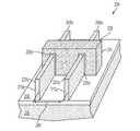
- FIG. 2shows a perspective view of a finFET, according to some embodiments
- FIG. 3shows a flowchart of a semiconductor processing method, according to some embodiments
- FIG. 4shows a perspective view of a finFET 402 after a portion of a fabrication process, according to some embodiments
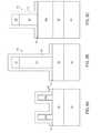
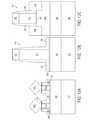
- FIGS. 5A, 5B, and 5Cshow cross-sectional views of finFET 402 along A-A′, B-B′, and C-C′, respectively, at the same stage of the fabrication process as illustrated in FIG. 4 , according to some embodiments;
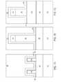
- FIGS. 6A, 6B, and 6Cshow cross-sectional views of finFET 402 along A-A′, B-B′, and C-C′, respectively, after another portion of a fabrication process, according to some embodiments;
- FIGS. 7A, 7B, and 7Cshow cross-sectional views of finFET 402 along A-A′, B-B′, and C-C′, respectively, after another portion of a fabrication process, according to some embodiments;
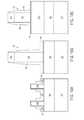
- FIGS. 8A, 8B, and 8Cshow cross-sectional views of finFET 402 along A-A′, B-B′, and C-C′, respectively, after another portion of a fabrication process, according to some embodiments;
- FIGS. 9A, 9B, and 9Cshow cross-sectional views of finFET 402 along A-A′, B-B′, and C-C′, respectively, after another portion of a fabrication process, according to some embodiments;
- FIGS. 10A, 10B, and 10Cshow cross-sectional views of finFET 402 along A-A′, B-B′, and C-C′, respectively, after another portion of a fabrication process, according to some embodiments;
- FIGS. 11A, 11B, and 11Cshow cross-sectional views of finFET 402 along A-A′, B-B′, and C-C′, respectively, after another portion of a fabrication process, according to some embodiments.
- FIGS. 12A, 12B, and 12Cshow cross-sectional views of finFET 402 along A-A′, B-B′, and C-C′, respectively, after another portion of a fabrication process, according to some embodiments.
- the FD-SOI FETmay comprise a source region 120 , a gate structure 130 , 135 , a drain region 140 , and a channel region 150 .
- the source, channel, and drain regionsmay be formed in a thin semiconductor layer 112 that is formed adjacent an insulating layer 105 (e.g., a thin insulating layer or buried oxide layer).
- the insulating layer 105may be formed adjacent a substrate layer 110 .
- the substrate layer 110 , insulating layer 105 , and thin semiconductor layer 112may collectively form a silicon-on-insulator (SOI) substrate 114 .
- the semiconductor layer 112 and insulating layer 105are ultrathin, e.g., less than about 35 nm or less than about 20 nm. Such devices may be referred to as ultra-thin body and buried oxide (UTBB) devices.
- UTBBultra-thin body and buried oxide
- the insulating layer 105may be less than about 30 nm in thickness, with a preferred thickness of about 25 nm for some embodiments, and the semiconductor layer 112 may be less than about 10 nm, with a preferred thickness of about 7 nm for some embodiments, for example.
- trench isolation structures 170comprising electrically-insulating material may be formed around one or more FD-SOI FETs.
- the gate structuremay comprise a gate conductor 130 and a thin gate insulator 135 .
- integrated source S, gate G, drain D, and body B interconnectsmay be formed to provide electrical connections to the source, gate, drain, and back body regions of the FD-SOI FET.
- the source region 120 and drain region 140 of an FD-SOI FETmay be doped with acceptor or donor impurities to form regions of a first conductivity type (e.g., p-type or n-type).
- the channel region 150may be doped to be of an opposite conductivity type, and may be of a same conductivity type as a back body region 115 (e.g., partially-depleted SOI or PD-SOI).
- the channel region 150may be undoped (FD-SOI).
- An FD-SOI FETcan exhibit reduced leakage currents compared to bulk FET devices and offer flexible bias strategies for improving speed or reducing threshold voltages for low-voltage applications.
- a finFET 200is depicted in the perspective view of FIG. 2 , according to some embodiments.
- a finFETmay be fabricated on a bulk semiconductor substrate 206 , e.g., a bulk silicon substrate, and comprise one or more fin-like structures ( 215 a , 215 b ) that run in a length direction along a surface of the substrate and extend in a height direction normal to the substrate surface.
- the fins 215may have narrow widths, e.g., less than 50 nanometers.
- the fins 215may pass through the insulating layer 205 , but be attached to the semiconducting substrate 206 at a lower region (e.g., “base”) of the fin.
- a gate structure 230comprising a conductive gate material 231 (e.g., polysilicon) and a gate insulator ( 235 a , 235 b ) (e.g., an oxide and/or a high dielectric constant material) may be formed over a region of the fin.
- the finFETmay further include a source region ( 220 a , 220 b ) and drain region ( 240 a , 240 b ) adjacent to the gate.
- a finFETmay also include integrated source S, gate G, drain D, and body B interconnects (not shown) to provide electrical connections to the source, gate, drain, and back body regions of the device.
- the entire fin portion encased by the gate structuremay be inverted and form a bulk channel rather than a surface channel.
- a metallic filmmay be deposited between a gate electrode 231 and gate oxide 235 (e.g., to improve gate conductance and/or gate switching speeds).
- FinFETs like the finFET depicted in FIG. 2may exhibit favorable electrostatic properties for scaling to high-density, low-power, integrated circuits. Because the fin and channel are raised from the substrate, cross-coupling between proximal devices may be reduced relative to cross-coupling between conventional FETs.
- the fins 215may be formed from the bulk substrate 206 by an etching process, and therefore may be attached to the substrate 206 at base regions of the fins, regions which are occluded in the drawing by the adjacent insulator 205 .
- the insulator 205may be formed after the etching of the fins 215 . Because the fins 215 are attached to the semiconductor substrate, leakage current and cross-coupling may occur via the base region of the fin.
- finFETsmay be formed on an SOI substrate.
- the finsWhen a finFET is formed on an SOI substrate, the fins may be attached to the thin semiconductor layer of the SOI substrate at base regions of the fins, or the fins may be formed by etching through the insulating layer of the SOI substrate such that the base regions of the fins are attached to the substrate layer of the SOI substrate.
- Source, channel, and drain regions of a finFETmay be doped with donor or acceptor impurities to create different regions of different conductivity types.
- source region 220 and drain region 240may be doped to be of a first conductivity type and the channel region 250 may be doped to be of an opposite conductivity type (or may be undoped).
- source region and drain regionas used may include extension regions of the fins that lie between source and drain contact regions and the channel region of the finFET device.
- the finFETmay further include a body region that may be of a same conductivity type as the channel region, or undoped (e.g., like the channel region).
- the doping of source and drain regions in a finFETmay be of various geometries.
- vertical portions of the fin 215may be doped to form source 220 and drain 240 regions.
- outer sheath portions of a fin 215may be doped to form source and drain regions.
- Some techniques for forming a strained film on and/or in the source/drain regions of a finFETinvolve etching the fins to reduce the fin height, and selectively forming strain-inducing material on the etched fins.
- the inventorshave recognized that with such techniques, careful control over the etch-back of the fins is desirable, for several reasons.
- An over-etched finmay lead to insufficient channel strain, because there may not be enough remaining fin to sufficiently impart strain to the channel region, or the fin may be totally removed leaving no seed for subsequent growth of the strain-inducing material.
- An under-etched finmay lead to insufficient channel strain, because it may not be possible to grow enough strain-inducing material to sufficiently strain the fin and impart that strain to the channel region.
- lack of uniformity in the etch-back of the fins across a wafer or chipmay lead undesirably to widely varying channel strains and performance of finFETs at different locations on the wafer or chip.
- the inventorshave conceived of techniques and structures for carefully controlling the etch-back of fins.
- the etch-back of finsmay be limited by one or more layers formed adjacent the fins. As a result, the heights of the etched-back fins and the strain applied to the finFET channels may be more uniform when this technique is used.
- self-limiting techniques for etching back finsmay be highly tolerant to variations in the etch rate at different locations on a wafer or chip.
- FIG. 3shows a flowchart that provides an overview of a semiconductor processing method 300 , according to some embodiments.
- one or more layersmay be formed over a substrate.
- the one or more layersmay be etched at least in regions adjacent to one or more fins.
- the one or more finsmay be etched to a height, determined, at least in part, by at least one of the one or more layers.
- FIG. 4shows a cross-sectional view of a finFET 402 at a stage of fabrication prior to performing the acts of semiconductor processing method 300 , according to some embodiments.
- FIGS. 5A, 5B , and SCshow cross-sections of finFET 402 along A-A′, B-B′, and C-C′, respectively, at the same stage of fabrication as illustrated in FIG. 4 , according to some embodiments.
- FinFET 402may be formed on an SOI substrate 414 having a substrate layer (e.g., silicon substrate layer) 410 and a buried insulating layer 405 (e.g., buried oxide layer).
- Buried insulator 405may include, but is not limited to, one or more layers of silicon oxide and/or any other suitable electrically-insulating material.
- FIG. 4illustrates an SOI substrate 414
- the techniques described hereinare not limited to devices formed on SOI substrates, and may be applied to devices formed on bulk substrates (e.g., bulk silicon substrates), and/or any other suitable substrates.
- FinFET 402may include one or more fins 415 .
- the fin(s)may be formed on the substrate by any suitable process (e.g., using sidewall image transfer (SIT) techniques, a mandrel process, lithographically patterning a resist and etching portions of the substrate to form the fin(s), or by patterning and etching trenches and depositing semiconductor material in the trenches to form the fins).
- lithographic patterningmay be done using extreme ultraviolet (EUV) lithography.
- the fins ( 415 a , 415 b )may have widths between approximately 3 nm and approximately 15 nm, and between approximately 3 nm and approximately 10 nm in some embodiments.
- the finsmay have heights between approximately 20 nm and approximately 50 nm.
- finFET 402may include a base layer 450 formed over the substrate.
- base layer 450may be formed over one or more fins 415 and/or over buried insulator 405 .
- the base layermay be disposed adjacent to and/or on a top surface of a fin.
- the base layermay be disposed adjacent to and/or on side surfaces of a fin.
- the base layerconformally coats the fin, and forms a substantially uniformly-thick layer on exposed surfaces of the fin. In the example of FIG.
- base layer 450is disposed adjacent to and on the top and side surfaces of fins 415 a and 415 b , such that base layer 450 covers fins 415 a and 415 b , and also covers portions of buried insulator 405 .
- Base layer 450may include one or more layers and/or materials (e.g., insulating materials), including, but not limited to, silicon oxide, ethylene-type oxide (e.g., ethylene oxide, ethylene glycol oxide), any other suitable oxide, and/or any other suitable insulating material.
- base layer 450may have a thickness between approximately 2 nm and approximately 4 nm.
- Base layer 450may exhibit etch selectivity over the fin material. For example, some embodiments of base layer 450 may be etched with a dry or wet etching process that does not appreciably etch the fin material, so as to remove the base layer and leave the fin.
- the base layer 450forms a gate oxide layer of the gate structure 430 .
- Base layer 450may be formed over the substrate by any suitable process that deposits or otherwise forms a layer of suitable material at least over one or more fins. In some embodiments, the base layer may be formed locally on the substrate to cover one or more fins within a selected region of the substrate.
- FinFET 402may include a gate structure 430 .
- the gate structure 430may at least partially surround at least a portion of the finFET's one or more fins 415 and the base layer 450 .
- the gate structuremay be formed by depositing one or more layers over the substrate, and by using lithographic techniques to pattern a gate structure over the fins.
- a polysilicon layermay be deposited over the fins, and may be planarized.
- a hard mask(e.g., a silicon nitride mask) may be deposited and patterned over the poly-silicon layer. The hard mask may be patterned using photolithography techniques and etching. The pattern of the hard mask may be transferred to the polysilicon via etching to form the gate structure.
- gate structure 430may include a gate portion 433 , a gate insulator 450 , and a spacer structure 480 .
- gate portion 433may comprise a gate conductor.
- a gate conductormay include one or more layers and/or materials (e.g., one or more layers of polysilicon and/or metallic material) configured such that a voltage applied thereto controls a current between the finFET's source and drain.
- a spacer structure 480may include one or more layers and/or materials (e.g., one or more nitride layers) disposed at sidewalls of the gate portion adjacent source and drain regions of the finFET.
- a gate insulator 450may include one or more layers and/or materials disposed adjacent to the finFET channel and configured to insulate the gate portion from the channel (e.g., one or more layers of silicon oxide, ethylene-type oxide, and/or any other suitable insulating material). Other suitable techniques and materials may be used in other embodiments to form the gate structure.
- gate portion 433may include a sacrificial gate.
- a sacrificial gatemay include one or more layers and/or materials formed as a “dummy gate” for the finFET 402 , and subsequently removed prior to formation of the finFET's final gate structure.
- FIGS. 6A-12Cdepict various stages in the formation of finFET 402 , according to some embodiments.
- FIGS. 6A-12Adepicts a cross-section of finFET 402 along A-A′.
- FIGS. 6B-12Bshows a cross-section of finFET 402 along B-B′.
- FIGS. 6C-12Cdepicts a cross-section of finFET 402 along C-C′.
- one or more layersmay be formed over the substrate.
- the one or more layers formed over the substratemay include a spacer layer 480 .
- spacer layer 480may be formed adjacent gate portion 433 and/or adjacent one or more fins 415 .
- spacer layer 480may be disposed on one or more exposed surfaces of gate portion 433 , and may also be disposed on one or more surfaces of a hard mask 470 at a top surface of the gate structure.
- the spacer layermay also be disposed at one or more exposed surfaces of a fin and/or on base layer 450 adjacent one or more fins.
- spacer layer 480may conformally cover one or more fins 415 and/or base layer 450 at a substantially uniform thickness. In some embodiments, spacer layer 480 may have a thickness between approximately 5 nm and 15 nm, between approximately 5 nm and approximately 10 nm, or between approximately 6 nm and approximately 9 nm.
- spacer layer 480may include, but is not limited to, a nitride (e.g., silicon nitride, SiOCN, SiPCN, and/or any other suitable nitride), a boron silicide (SiB), any material suitable for forming a gate spacer structure, and/or any other suitable material.
- a nitridee.g., silicon nitride, SiOCN, SiPCN, and/or any other suitable nitride
- SiBboron silicide
- portions of spacer layer 480may be formed adjacent a gate portion 433 of finFET 400 , and may function as gate spacers. In some embodiments, portions of spacer layer 480 formed adjacent the finFET's gate portion 433 may have a thickness between approximately 5 and 10 nm. In some embodiments, a layer thickness of 5-10 nm adjacent to the finFET's gate structure may facilitate proper formation of the finFET source and drain regions. For example, a spacer layer 480 thickness of 5-10 nm may be used to carefully locate source and drain junctions, and subsequently used for gate conductor replacement.
- FIGS. 6A-6Cillustrate cross-sections of finFET 402 after formation of spacer layer 480 , according to some embodiments.
- spacer layer 480is formed adjacent to top and side surfaces of fins 415 a and 415 b , such that spacer layer 480 covers the fins and the portions of base layer 450 formed on the fins.
- spacer layer 480is formed adjacent to side and top surfaces of gate portion 433 and hard mask 470 , such that spacer layer 480 covers gate portion 433 and hard mask 470 .
- hard mask 470may be removed before spacer layer 480 is formed.
- spacer layer 480is formed on base layer 450 over buried insulator 405 at least in regions adjacent to the fins 415 and/or the gate structure 430 .
- the one or more layers formed over the substrate in act 302may include a second layer 485 .
- the second layer 485may exhibit etch selectivity over the spacer layer 480 .
- second layer 485may be formed on spacer layer 480 .
- portions of second layer 485may be formed adjacent a top surface and/or one or more side surfaces of a fin 415 .
- portions of second layermay be formed adjacent a top surface and/or one or more side surfaces of gate structure 430 .
- second layer 485may be a planarizing layer that covers fins 415 , portions of regions adjacent the fins 415 , and all or some of the gate structure 430 .
- second layer 485may comprise an organic planarization layer (OPL).
- OPLorganic planarization layer
- the OPLmay comprise polyimide, polymethyl methacrylate, polymethylisopropenyl ketone, photoresists, or any suitable polymer.
- the OPLmay comprise a spin-on glass.
- the second layer 485may comprise a developable organic planarization layer (developable OPL).
- the developable OPLmay include a light-sensitive material which, when exposed to radiation (e.g., electromagnetic radiation), is chemically altered such that a layer at the exposed surface of the developable organic PL may be removed using a developing solvent.
- the light-sensitive materialmay comprise polyacrylate resin, epoxy resin, phenol resin, polyamide resin, polyimide resin, unsaturated polyester resin, polyphenylenether resin, polyphenylenesulfide resin, benzocyclobutene (BCB), and/or any organic polymer and a photo-active compound having a molecular structure that can attach to the molecular structure of the organic polymer.
- polyacrylate resinepoxy resin, phenol resin, polyamide resin, polyimide resin, unsaturated polyester resin, polyphenylenether resin, polyphenylenesulfide resin, benzocyclobutene (BCB), and/or any organic polymer and a photo-active compound having a molecular structure that can attach to the molecular structure of the organic polymer.
- second layer 485may comprise one or more materials having a thickness which can be accurately and uniformly reduced by a timed etch process.
- the one or more materialsmay include, but are not limited to organic planarization layer (OPL) and/or organic development layer (ODL).
- second layer 485may be planarized.
- Second layer 485may be planarized using any suitable planarization technique, including, but not limited to, chemical-mechanical polishing. After planarization, the top surface of second layer 485 may be substantially flat.
- the thickness of second layer 485may be between approximately 100 nm and 2 ⁇ m. The thickness of the second layer 485 may be predetermined with high accuracy. In some embodiments, the thickness of the second layer 485 may be measured after planarization, e.g., by ellipsometry.
- FIGS. 7A-7Cillustrate cross-sections of finFET 402 after formation of second layer 485 , according to some embodiments.
- second layer 485is formed over spacer layer 480 in at least regions where the fins 415 and the gate structures 430 are located.
- second layer 485is planarized.
- the one or more layers formed in act 302 of method 300include a spacer layer 480 and a second layer 485
- some embodimentsare not limited to formation of spacer layer 480 and second layer 485 .
- the number of layers formed in act 302may be one, three, or more than three.
- one or more layersmay be etched in a region adjacent a fin.
- the one or more etched layersmay include second layer 485 , which may be etched using a first etch process.
- the first etch processmay be anisotropic. Though, in some embodiments, the first etch process may be isotropic.
- the first etch processmay include, but is not limited to, a timed etch process, and/or any other suitable type of etch process.
- a timed etch processthe extent (e.g., depth) to which a layer is etched may be controlled approximately based on the etch time and the etch rate.
- the etch rate of second layer 485 during the first etch processmay be approximately uniform across the wafer and/or chip.
- the first etch processmay be controlled such that, at the completion of the first etch process, a top surface of second layer 485 is below a top surface of a fin 415 in a region adjacent the fin (e.g., a height of second layer 485 above the substrate may be less than a height of a fin above the substrate, at least in a region adjacent to the fin).
- a selected amount of the fin 415can be exposed above the second layer 485 , as depicted in FIG. 8A .
- the first etch processmay etch second layer 485 without etching spacer layer 480 or with negligible etching of spacer layer 480 .
- exposed surfaces of second layer 485may be etched at a higher rate than exposed surfaces of spacer layer 480 (e.g., the etch rate of second layer 485 during the first etch process may be at least 3, 5, 10, 20, 50, or 100 times higher than the etch rate of spacer layer 480 ).
- the etch rate of second layer 485 during the first etch processmay be at least 3, 5, 10, 20, 50, or 100 times higher than the etch rate of spacer layer 480 ).
- portions of spacer layer 480may remain above the second layer 485 after the first etch process.
- the different etch rates for the first and second layersmay be determined by the characteristics of the first and second layers (e.g., materials, geometry), and/or by characteristics of the first etch process.
- the first etch processmay be performed during a processing sequence for patterning the spacer layer 480 (e.g., gate spacer patterning).
- the first etch processmay not add any additional masking steps to the finFET fabrication process.
- the first etchadds a timing requirement to an etch to reveal the gate structure during a gate spacer patterning process.
- FIGS. 8A-8Cillustrate cross-sections of finFET 402 after etching second layer 485 , according to some embodiments.
- second layer 485has been etched to a depth below the top surfaces of fins 415 a and 415 b , such that the top surface of second layer 485 is below the top surfaces of the fins in regions adjacent to the fins.
- the second layer 485is etched back to reveal approximately one-half of the fin height.
- the surface of the second layer 485is etched back to a level approximately half way between the top and bottom of the fin.
- the revealed height of the fincan be controlled to within about ⁇ 5 nm in some embodiments, and to within about ⁇ 2 nm in some embodiments. Since the second layer is planarized before the etch, the amount of fin revealed is uniform across the substrate to within ⁇ 10 nm in some embodiments, and within ⁇ 5 nm in some embodiments.
- the one or more layers etched in act 304may further include spacer layer 480 , which may be etched using a second etch process.
- the second etch processmay be anisotropic. Though, in some embodiments, the second etch process may be isotropic. In some implementations, the second etch process may be mostly anisotropic, but include some isotropic etching.
- the second etch processmay etch spacer layer 480 without etching (or with negligible etching of) second layer 485 , base layer 450 , and/or fins 415 .
- exposed surfaces of spacer layer 480may be etched at a higher rate than exposed surfaces of second layer 485 , base layer 450 , and/or fins 415 (e.g., the etch rate of spacer layer 480 may be at least 3, 5, 10, 20, 50, or 100 times higher than the etch rates of second layer 485 , base layer 450 , and/or fins 415 .
- the different etch rates for the first layer and the other layers and/or structuresmay be determined by characteristics (e.g., materials, geometry) of the layers and/or structures, and/or by characteristics of the second etch process.
- the second etch processmay comprise, but is not limited to, a self-limiting etch process.
- the extent (e.g., depth) to which at least some portions of an etched layer are etchedmay be determined, at least in part, by characteristics of layers and/or structures adjacent the etched layer (e.g., by the presence and/or etch rate of a fin structure, gate structure, and/or layer above and/or adjacent to the etched layer), and/or by the width of an exposed surface of the etched layer.
- etchingmay not occur, may be negligible, or may occur slowly when the width of an exposed surface of the etched layer is less than a threshold width.
- the second etch processmay be self-limited, at least in part, by second layer 485 .
- the height of the etched spacer layer 480may be determined, at least in part, by a thinness of the spacer layer 480 and presence of second layer 485 and base layer 450 adjacent to the spacer layer.
- the exposed spacer layer 480may be etched back to a level substantially co-planar with a top surface of second layer 485 , according to some embodiments. Because of the thinness of the spacer layer 480 and presence of adjacent layers which do not appreciably etch, the spacer layer etching may self limit at approximately the surface of the second layer 485 . When this surface is reached, the etch rate of the spacer layer 480 may reduce significantly, e.g., by a factor of two or more.
- the second etch processmay additionally etch spacer layer 480 in a region adjacent to gate structure 430 to form gate spacers.
- the forming of the gate spacersmay be done simultaneously with etch back of the spacer layer 480 at the fins.
- a same etch processing stepmay be applied to form the gate spacers and to etch back spacer layer 480 in a region adjacent to a fin 415 .
- FIGS. 9A-9Cillustrate cross-sections of finFET 402 after etching spacer layer 480 , according to some embodiments.
- spacer layer 480is etched to approximately the surface of second layer 485 in the regions adjacent fins 415 a and 415 b , such that the surface of spacer layer 480 is substantially co-planar with the surface of second layer 485 (e.g., the height of spacer layer 480 is within approximately ⁇ 2 nm of the height of second layer 485 in some embodiments, and within approximately ⁇ 1 nm of the height of second layer 485 in some embodiments) in the regions adjacent the fins.
- FIGS. 9A-9Cillustrate cross-sections of finFET 402 after etching spacer layer 480 , according to some embodiments.
- spacer layer 480is etched to approximately the surface of second layer 485 in the regions adjacent fins 415 a and 415 b , such that the surface of spacer layer 480 is substantially co-planar with the surface of
- the etch-back of spacer layer 480removes spacer layer 480 from the top of fin 415 and from the upper portions of the sides of fin 415 .
- the etch-back of spacer layer 480may be self-limited to approximately the surface of second layer 485 near the fins because the width of the exposed surface of spacer layer 480 near the fins may be quite small (e.g., between approximately 5 nm and 15 nm, or between approximately 5 nm and 10 nm) making it difficult for the etchant to reach the portions of spacer layer 480 below the surface of second layer 485 , and because the layers adjacent to the exposed surface of spacer layer 480 (e.g., second layer 485 and base layer 450 ) may have low etch rates during the second etch process.
- the etch to remove the spacer layermay be isotropic, so that exposed regions of the spacer layer etch more quickly than narrow regions sandwiched between layers having low etch rates.
- a third etch processmay or may not be performed to etch second layer 485 .
- the third etch processmay result in the removal of second layer 485 from the wafer or chip.
- the third etch processmay include any suitable etch technique, including, but not limited to, the same etch technique used in the first etch process, a timed etch technique, a self-limited etch technique, and/or any other suitable etch technique.
- the third etch processmay remove second layer 485 without etching base layer 450 (or with negligible etching of base layer 450 ).
- the third etch processmay also remove exposed regions base layer 450 , and the etching of base layer 450 may be self-limited.
- the third etch processmay be anisotropic.
- the second etch processmay be isotropic.
- the remaining portions of second layer 485may remain on the wafer or chip at least until the etch-back of the fins 415 is performed.
- FIGS. 10A-10Cillustrate cross-sections of finFET 402 after removal of second layer 485 , according to some embodiments.
- portions of spacer layer 480remain in regions adjacent gate structure 430 (e.g., as gate spacers) and in regions adjacent to the sides of fins 415 .
- one or more finsmay be etched to a height determined, at least in part, by one or more of the layers formed in act 302 .
- the fins 415may be etched back using any suitable etch technique, including, but not limited to, anisotropic etching and/or isotropic etching.
- anisotropic etching and/or isotropic etchingmay result in enhanced channel strain and/or result in the source/drain regions of the finFET being positioned closer to the channel region, because isotropic etching may remove some portions of fin 415 located below the gate spacers in a region adjacent to the finFET channel.
- a fin etch processmay etch one or more fins 415 and the portions of base layer 450 covering the fins 415 without etching spacer layer 480 and/or second layer 485 (or with negligible etching of spacer layer 480 and/or second layer 485 ).
- exposed surfaces of fin 415 and base layer 450may be etched at a higher rate than exposed surfaces of spacer layer 480 and/or second layer 485 (e.g., the etch rate of the fins 415 and/or base layer 450 may be at least 3, 5, 10, 20, 50, or 100 times higher than the etch rates of spacer layer 480 and/or second layer 485 ).
- the different etch rates for the respective layers and structuresmay be determined by characteristics (e.g., geometry, materials) of the layers and/or structures, and/or by characteristics of the fin etch process.
- the fin etch processmay include, but is not limited to, at least one self-limiting etch process, and/or any other suitable type of etch process.
- the fin etch processmay comprise two self-limiting etches.
- a first self-limiting etchmay be used to etch back the base layer 450 to a height of approximately the spacer layer 480 at the sides of the fins.
- the base layer etch processmay be self-limited, at least in part, by a thinness of the base layer and the presence of the spacer layer 480 and/or the second layer 485 .
- the height of the etched base layer 450may be determined, at least in part, by spacer layer 480 and/or second layer 485 (e.g., the top surface of base layer 450 may be substantially co-planar with a top surface of spacer layer 480 and/or a top surface of second layer 485 ) adjacent to a fin 415 , as depicted in FIG. 11A .
- a second self-limiting etchmay then be used to etch back the fin to a height of approximately the spacer layer 480 at the sides of the fins.
- the fin etch processmay be self-limited, at least in part, by a thinness of the fin and the presence of the spacer layer 480 and/or second layer 485 .
- the height of the etched fin 415may be determined, at least in part, by spacer layer 480 and/or second layer 485 (e.g., the top surface of the etched fin 415 may be substantially co-planar with a top surface of spacer layer 480 and/or a top surface of second layer 485 ) adjacent to a fin 415 , as depicted in FIG. 11A .
- the fin etch processmay comprise a single self-limiting etch, in which both the base layer 450 and the fin 415 are etched back to a height of approximately the space layer 480 at the sides of the fins.
- the combined etch processmay be self-limited, at least in part, by a thinness of the base layer and fin together, and by the presence of the spacer layer 480 and/or the second layer 485 .
- the height of the etched base layer 450 and the fin 415may be determined, at least in part, by spacer layer 480 and/or second layer 485 (e.g., the top surface of base layer 450 and the top surface of fin 415 may be substantially co-planar with a top surface of spacer layer 480 and/or a top surface of second layer 485 ) adjacent to a fin 415 , as depicted in FIG. 11A .
- the self-limiting etchesmay result in an etched layer height that is below a height of adjacent layers.
- the etched fin 415may self-limit to a height that is a few nanometers (e.g., approximately 1 to 5 nanometers) below the upper surface of the spacer layer 480 . Accordingly, the height of the spacer layer may be increased to account for the difference in etch heights between the etched layer and non-etched layers.
- FIGS. 11A-11Cillustrate cross-sections of finFET 402 after etching one or more fins 415 , according to some embodiments.
- base layer 450 and fins 415are etched to approximately the surface of spacer layer 480 in the regions adjacent the sides of the fins.
- the top surfaces of the fins (and the top portions of base layer 450 adjacent the sides of the fins)may be substantially co-planar with the top edges of spacer layer 480 adjacent the sides of the fins (e.g., the height of the fins 415 and base layer 450 may be within approximately 1-2 nm of the top edges of the spacer layer 480 ).
- the height of the etched fins 415may be between approximately 20 nm and 50 nm.
- the etch-back of the fins 415may be self-limited to approximately the top edges of spacer layer 480 adjacent the fins, (1) because the width of the opening formed by the base layer 450 (between the spacer layer 480 and the fin 415 ) may be quite small (e.g., approximately 2 nm-4 nm), making it difficult for the etchant to reach portions of base layer 450 , and because the layers adjacent to the top surface of the base layer 450 may have low etch rates during the base layer etch process, (2) because the width of the opening formed by the fin 415 (between portions of the spacer layer 480 and portions of the base layer 450 adjacent to the sides of the fin) may be quite small (e.g., approximately 3 nm-10 nm), making it difficult for the etchant to reach portions of fin 415 , and because the layers adjacent to the top surface of the fin 415 may have low etch rates during the fin etch process, and/or (
- some portions 416 of the fins 415 covered by gate structure 430 and/or the gate spacersmay be etched during etch back of the fins.
- an isotropic etch processmay be used in addition to an anisotropic etch to increase the amount of portions 416 removed.
- an optional etch processmay be performed to etch portions of spacer layer 480 .
- this optional etch processmay result in the removal of spacer layer 480 from regions adjacent the fins 415 .
- this optional etch processmay not result in the removal of the gate spacers.
- This optional etch processmay include any suitable etching technique, including, but not limited to, the same etch technique used in the second etch process, a timed etch technique, and/or any other suitable etch technique.
- the optional etch processmay be anisotropic.
- the optional etch processmay not be performed, and portions of spacer layer 480 may remain in regions adjacent to the fins 415 at the end of the finFET fabrication process.
- method 300may include an act (not illustrated in FIG. 3 ) of inducing strain in the finFET channel.
- the channel strainmay be induced using any suitable technique, including, but not limited to, selectively forming (e.g., growing or depositing) strain-inducing material in and/or on the exposed portions of the fins 415 .
- a materiale.g., SiGe
- SiGemay be formed under compressive stress at the source and/or drain regions of a finFET using an epitaxial growth process, thereby inducing strain in the finFET's channel.
- a materiale.g., SiN and/or SiC
- a materialmay be formed under tensile stress at the source and/or drain regions of an finFET using an epitaxial growth process, thereby inducing an opposite strain in the finFET's channel. Accordingly, appropriate channel strains may be induced for p-channel and n-channel devices of CMOS integrated circuits.
- FIGS. 12A-12Cillustrate cross-sections of finFET 402 after growing strain-inducing materials ( 490 a , 490 b ) at source and drain regions of the fins 415 .
- a material 490 a , 490 b formed under compressive stress on the source and drain regionsimparts compressive strain to the channel region of the finFET.
- a material 490 a , 490 b formed under tensile stress on the source and drain regionsimparts tensile strain to the channel region of the finFET.
- Imparting opposite strains on a same substratemay be done by masking a first portion of the fins during a first epitaxial growth of strain-inducing material at a second portion of the fins, and masking the second portion of the fins during a second epitaxial growth of strain-inducing material at the first portion of the fins.
- the technology described hereinmay be embodied as a method, of which at least one example has been provided.
- the acts performed as part of the methodmay be ordered in any suitable way. Accordingly, embodiments may be constructed in which acts are performed in an order different than illustrated, which may include performing some acts simultaneously, even though shown as sequential acts in illustrative embodiments. Additionally, a method may include more acts than those illustrated, in some embodiments, and fewer acts than those illustrated in other embodiments. Additional acts of a method not illustrated in FIG. 3 may include, but are not limited to, doping the drain/source regions of the device (e.g., by ion implantation), replacing a sacrificial gate with a gate conductor, and/or any other suitable act.
- an act of “forming” a layermay include any suitable process that deposits, grows, coats, transfers, or otherwise forms a layer of material on a wafer or die, including, but not limited to, epitaxy, physical vapor deposition (PVD), chemical vapor deposition (CVD), electrochemical deposition (ECD), molecular beam epitaxy (MBE), sputtering, e-beam evaporation, and/or atomic layer deposition (ALD).
- PVDphysical vapor deposition
- CVDchemical vapor deposition
- ECDelectrochemical deposition
- MBEmolecular beam epitaxy
- ALDatomic layer deposition
- forming a layermay comprise additive processes (processes which add material to the wafer or die), modification processes (processes which modify properties of material on the wafer or die), and/or removal processes (processes which remove material from the wafer or die, e.g., etching).
- additive processesprocesses which add material to the wafer or die
- modification processesprocesses which modify properties of material on the wafer or die
- removal processesprocesses which remove material from the wafer or die, e.g., etching
- an act of “etching” a material or a layermay include any suitable process that removes material from a wafer or die, including, but not limited to, wet etching, dry etching, plasma etching, isotropic etching, anisotropic etching, timed etching, and/or self-limited etching.
- a portion of the waferis protected from the etchant by a masking material (“mask”) which resists the etching, including, but not limited to a patterned photoresist or hard mask.
- strained source/drainmay refer to a source region and/or a drain region that is compressively or tensiley strained, e.g., by the formation of a strain-inducing material at the source/drain region.
- recessed source/drainmay refer to a source region and/or a drain region formed, at least in part, by recessing (e.g., etching) a structure, including, without limitation, a fin.
- recessinge.g., etching
- the process of recessing the structure (e.g., fin) that forms at least a portion of the source region and/or drain regionmay leave one or more indicia of the structure's recessed nature on the remaining portion of the recessed structure or elsewhere on the semiconductor device.
- the “top” of a finmay refer to a surface of the fin that is farthest from the substrate surface over which the fin is formed. In some embodiments, the top of the fin may be approximately parallel to the substrate surface over which the fin is formed.
- CMOS devicesmay be formed by applying the above-described technique (e.g., method 300 ) during formation of n-channel finFETs and during formation of p-channel finFETs.
- a semiconductor processing methodcomprising: conformally depositing a first layer over a fin configured to form a portion of a finFET; depositing a second layer to cover the fin and the first layer; etching the second layer to expose the first layer in a region adjacent the fin; and etching the first layer in the region adjacent the fin to approximately a surface of the second layer.
- the transistorsmay be incorporated as part of microprocessing or memory circuitry for digital or analog signal processing devices.
- the transistorsmay be incorporated in logic circuitry, in some implementations.
- the transistorsmay be used in consumer electronic devices such as smart phones, computers, televisions, sensors, microprocessors, microcontrollers, field-programmable gate arrays, digital signal processors, application specific integrated circuits, logic chips, analog chips, and digital signal processing chips.
- the methods and structuresmay be employed for variations of finFET devices in some embodiments.
- the methods and structuresmay be employed for the fabrication of tri-gate, pi-gate, or omega-gate transistors.
- the methods and structuresmay be employed for the fabrication of gate-all-around (GAA) transistors.
- GAAgate-all-around
- the terms “approximately,” “substantially,” and “about”may be used to mean within ⁇ 20% of a target dimension in some embodiments, within ⁇ 10% of a target dimension in some embodiments, within ⁇ 5% of a target dimension in some embodiments, and yet within ⁇ 2% of a target dimension in some embodiments.
- the terms “approximately,” “substantially,” and “about”may include the target dimension.
Landscapes
- Engineering & Computer Science (AREA)
- Physics & Mathematics (AREA)
- General Physics & Mathematics (AREA)
- Power Engineering (AREA)
- Microelectronics & Electronic Packaging (AREA)
- Computer Hardware Design (AREA)
- Manufacturing & Machinery (AREA)
- Condensed Matter Physics & Semiconductors (AREA)
- Theoretical Computer Science (AREA)
- Health & Medical Sciences (AREA)
- Artificial Intelligence (AREA)
- Evolutionary Computation (AREA)
- Computational Linguistics (AREA)
- General Engineering & Computer Science (AREA)
- Software Systems (AREA)
- Molecular Biology (AREA)
- Computing Systems (AREA)
- Multimedia (AREA)
- Acoustics & Sound (AREA)
- Mathematical Physics (AREA)
- General Health & Medical Sciences (AREA)
- Human Computer Interaction (AREA)
- Audiology, Speech & Language Pathology (AREA)
- Data Mining & Analysis (AREA)
- Biophysics (AREA)
- Biomedical Technology (AREA)
- Life Sciences & Earth Sciences (AREA)
- Thin Film Transistor (AREA)
Abstract
Description
- 1. Technical Field
- The present disclosure relates to methods of forming semiconductor devices having one or more fin structures (“fins”), and to semiconductor devices having one or more fins. Some embodiments described in the present disclosure relate to finFETs having strained channels and/or to methods for fabricating finFETs having strained channels.
- 2. Discussion of the Related Art
- Transistors are fundamental device elements of many modern digital processors and memory devices, and have found numerous applications in various areas of electronics including data processing, data storage, and high-power applications. Currently, there are a variety of transistor types and designs that may be used for different applications. Various transistor types include, for example, bipolar junction transistors (BJT), junction field-effect transistors (JFET), metal-oxide-semiconductor field-effect transistors (MOSFET), vertical channel or trench field-effect transistors, and superjunction or multi-drain transistors.
- Two types of transistors which have emerged within the MOSFET family of transistors show promise for scaling to ultra-high density and nanometer-scale channel lengths. One of these transistor types is a so-called fin field-effect transistor or “finFET.” The channel of a finFET is formed in a three-dimensional fin that may extend from a surface of a substrate. FinFETs have favorable electrostatic properties for complimentary MOS (CMOS) scaling to smaller sizes. Because the fin is a three-dimensional structure, the transistor's channel can be formed on three or more surfaces of the fin, so that the finFET can exhibit a high current switching capability for a given surface area occupied on substrate. Since the channel and device can be raised from the substrate surface, there can be reduced electric field coupling between adjacent devices as compared to conventional planer MOSFETs.
- The second type of transistor is called a fully-depleted, silicon-on-insulator or “FD-SOI” FET. The channel, source, and drain of an FD-SOI FET are formed in a thin planar semiconductor layer that overlies a thin insulator. Because the semiconductor layer and the underlying insulator are thin, the body of the transistor (which lies below the thin insulator) can act as a second gate. The thin layer of semiconductor on insulator permits higher body biasing voltages that can boost performance. The thin insulator also reduces leakage current to the transistor's body region relative to the leakage current that would otherwise occur in bulk FET devices.
- FET performance may be improved by adjusting the strain in the FET's channel to increase carrier mobility within the channel. For silicon FETs, device performance may be improved by applying compressive strain to a p-channel device, and/or by applying tensile strain to an n-channel device. In some cases, channel strain may be induced by straining the FET's source and/or drain regions, such that the strain is transferred through the source and/or drain regions to the channel.
- According to some embodiments, a method for forming fins of a finFET is provided, the method comprising: forming one or more layers over a semiconductor fin; etching the one or more layers in a region adjacent the fin to expose at least a portion of the fin; and etching the fin to a height determined, at least in part, by at least one of the one or more layers.
- In some embodiments, the etching of the fin is self-limited by at least a level of one of the one or more layers and by a width of an opening defined by the fin.
- In some embodiments, the width of the fin is between approximately 3 nm and approximately 10 nm.
- In some embodiments, etching the fin comprises etching the fin to approximately an adjacent surface of at least one of the one or more layers.
- In some embodiments, the one or more layers comprise a first layer covering the fin and a second layer covering the fin and the first layer.
- In some embodiments, etching the one or more layers comprises removing a portion of the second layer to expose the first layer in the region adjacent the fin.
- In some embodiments, removing the portion of the second layer comprises: planarizing the second layer; and performing a timed etch of the second layer to etch back a surface of the second layer to a level below the top of the fin.
- In some embodiments, the method further comprises forming the first layer as a spacer layer at the fin and at a gate conductor for the fin, wherein etching the one or more layers in the region adjacent the fin comprises etching the first layer to a height determined, at least in part, by a level of the second layer adjacent the fin.
- In some embodiments, etching the first layer comprises etching the first layer to approximately a surface of the second layer.
- In some embodiments, the etching of the first layer in the region adjacent the fin is self-limited by at least a level of the second layer and a width of the first layer in the region adjacent the fin.
- In some embodiments, the spacer layer comprises a nitride and etching the one or more layers further comprises etching the first layer at the gate conductor to form gate spacers.
- In some embodiments, the method further comprises removing the second layer after etching the first layer in the region adjacent the fin and before etching the fin.
- In some embodiments, etching the fin comprises etching the fin to approximately an edge of the first layer adjacent the fin.
- In some embodiments, the etching of the fin is self-limited, at least in part, by a location of the edge of the first layer and by a width of an opening defined by the fin.
- In some embodiments, etching the fin comprises etching the fin to approximately a surface of the second layer.
- In some embodiments, the etching of the fin is self-limited by at least a height of the first layer adjacent the fin and by a width of an opening defined by the fin.
- In some embodiments, forming the one or more layers comprises: conformally depositing the first layer over the fin to a thickness between approximately 5 nm and approximately 10 nm; and depositing the second layer to cover the fin and the first layer.
- In some embodiments, the method further comprises forming a spacer layer for a gate structure of the finFET in a same deposition step in which the first layer is deposited over the fin.
- In some embodiments, etching the fin comprises etching the fin at source and drain regions of the finFET, and the method further comprises growing strain-inducing material at the source and drain regions.
- In some embodiments, a lattice parameter of the strain-inducing material differs from a lattice parameter of the fin.
- In some embodiments, the strain-inducing material imparts a strain in a channel of the finFET.
- In some embodiments, the fin is formed from bulk silicon and the strain-inducing material comprises silicon germanium and/or silicon carbide.
- In some embodiments, the one or more layers further comprise a conformal insulating layer, wherein the method further comprises forming the conformal insulating layer on the fin prior to forming the first layer over the fin, and wherein etching the one or more layers comprises etching the conformal insulating layer.
- In some embodiments, the insulating layer forms a gate insulator for the finFET.
- In some embodiments, the second layer comprises an organic planarization layer.
- According to some embodiments, a finFET is provided, comprising: a fin having recessed source and drain regions; a spacer layer formed adjacent the side walls of the recessed source and drain regions; and strain-inducing material formed at the source and drain regions, wherein a height of the fin at the recessed source and drain regions is approximately equal to a height of the spacer layer adjacent the side walls of the recessed source and drain regions.
- In some embodiments, a width of the fin is between approximately 3 nm and approximately 10 nm.
- In some embodiments, the strain-inducing material comprises epitaxially-grown material.
- In some embodiments, the strain-inducing material is configured to impart strain to a channel region of the finFET.
- In some embodiments, a lattice parameter of the strain-inducing material differs from a lattice parameter of the fin.
- In some embodiments, the spacer layer comprises a conformal spacer layer, wherein the conformal spacer layer is also formed at a gate structure of the finFET.
- In some embodiments, the finFET further comprises a conformal oxide layer disposed on the side surfaces of the fin, between the fin and the spacer layer.
- In some embodiments, the spacer layer comprises one or more nitrides.
- In some embodiments, the finFET further comprises a gate structure formed adjacent the fin, wherein a portion of the spacer layer is formed adjacent the gate and is configured as a gate spacer.
- In some embodiments, the finFET is formed on a silicon-on-insulator (SOI) substrate.
- In some embodiments, the finFET is formed on a buried oxide (BOX) layer of the SOI substrate.
- In some embodiments, an integrated circuit comprises a plurality of the finFETs, wherein heights of the recessed source and drain regions of the fins are uniform across the integrated circuit to within ±2 nm.
- According to some embodiments, a method for self-limited etching of a narrow, raised structure is provided, comprising: forming the narrow, raised structure to have a width less than approximately 10 nm; depositing material adjacent the narrow, raised structure; removing a portion of the material to reveal a portion of the narrow, raised structure; and etching the narrow, raised structure to a level approximately equal to a level of the material adjacent the narrow, raised structure.
- In some embodiments, the narrow, raised structure comprises a fin for a finFET transistor.
- In some embodiments, the narrow, raised structure further comprises a conformal insulating layer formed over the fin.
- In some embodiments, depositing the material comprises forming a conformal layer of the material over the narrow, raised structure.
- In some embodiments, depositing the material comprises forming a planarized layer of the material over the narrow, raised structure.
- In some embodiments, removing a portion of the material comprises etching a surface of the planarized layer to a level below an upper surface of the narrow, raised structure.
- One of ordinary skill in the art will understand that the figures, described herein, are for illustration purposes only. It is to be understood that in some instances various aspects of the illustrated embodiments may be shown exaggerated or enlarged to facilitate an understanding of the embodiments. In the drawings, like reference characters generally refer to like features, functionally similar elements and/or structurally similar elements throughout the various figures. The drawings are not necessarily to scale, emphasis instead being placed upon illustrating the principles of the teachings. Where the drawings relate to fabrication of integrated devices, an illustrated device may be representative of a large plurality of devices that may be fabricated in parallel. The drawings are not intended to limit the scope of the present teachings in any way.
FIG. 1 shows an elevation view of an FD-SOI FET;FIG. 2 shows a perspective view of a finFET, according to some embodiments;FIG. 3 shows a flowchart of a semiconductor processing method, according to some embodiments;FIG. 4 shows a perspective view of afinFET 402 after a portion of a fabrication process, according to some embodiments;FIGS. 5A, 5B, and 5C show cross-sectional views offinFET 402 along A-A′, B-B′, and C-C′, respectively, at the same stage of the fabrication process as illustrated inFIG. 4 , according to some embodiments;FIGS. 6A, 6B, and 6C show cross-sectional views offinFET 402 along A-A′, B-B′, and C-C′, respectively, after another portion of a fabrication process, according to some embodiments;FIGS. 7A, 7B, and 7C show cross-sectional views offinFET 402 along A-A′, B-B′, and C-C′, respectively, after another portion of a fabrication process, according to some embodiments;FIGS. 8A, 8B, and 8C show cross-sectional views offinFET 402 along A-A′, B-B′, and C-C′, respectively, after another portion of a fabrication process, according to some embodiments;FIGS. 9A, 9B, and 9C show cross-sectional views offinFET 402 along A-A′, B-B′, and C-C′, respectively, after another portion of a fabrication process, according to some embodiments;FIGS. 10A, 10B, and 10C show cross-sectional views offinFET 402 along A-A′, B-B′, and C-C′, respectively, after another portion of a fabrication process, according to some embodiments;FIGS. 11A, 11B, and 11C show cross-sectional views offinFET 402 along A-A′, B-B′, and C-C′, respectively, after another portion of a fabrication process, according to some embodiments; andFIGS. 12A, 12B, and 12C show cross-sectional views offinFET 402 along A-A′, B-B′, and C-C′, respectively, after another portion of a fabrication process, according to some embodiments.- An example of a fully-depleted silicon-on-insulator (FD-SOI)
FET 100 is depicted inFIG. 1 , according to some embodiments. The FD-SOI FET may comprise asource region 120, agate structure drain region 140, and achannel region 150. The source, channel, and drain regions may be formed in athin semiconductor layer 112 that is formed adjacent an insulating layer105 (e.g., a thin insulating layer or buried oxide layer). The insulatinglayer 105 may be formed adjacent asubstrate layer 110. In some embodiments, thesubstrate layer 110, insulatinglayer 105, andthin semiconductor layer 112 may collectively form a silicon-on-insulator (SOI)substrate 114. In some implementations, thesemiconductor layer 112 and insulatinglayer 105 are ultrathin, e.g., less than about 35 nm or less than about 20 nm. Such devices may be referred to as ultra-thin body and buried oxide (UTBB) devices. In a UTBB structure, the insulatinglayer 105 may be less than about 30 nm in thickness, with a preferred thickness of about 25 nm for some embodiments, and thesemiconductor layer 112 may be less than about 10 nm, with a preferred thickness of about 7 nm for some embodiments, for example. In some embodiments,trench isolation structures 170 comprising electrically-insulating material may be formed around one or more FD-SOI FETs. The gate structure may comprise agate conductor 130 and athin gate insulator 135. According to some embodiments, integrated source S, gate G, drain D, and body B interconnects may be formed to provide electrical connections to the source, gate, drain, and back body regions of the FD-SOI FET. - In some embodiments, the
source region 120 and drainregion 140 of an FD-SOI FET may be doped with acceptor or donor impurities to form regions of a first conductivity type (e.g., p-type or n-type). Thechannel region 150 may be doped to be of an opposite conductivity type, and may be of a same conductivity type as a back body region115 (e.g., partially-depleted SOI or PD-SOI). In some implementations, thechannel region 150 may be undoped (FD-SOI). An FD-SOI FET can exhibit reduced leakage currents compared to bulk FET devices and offer flexible bias strategies for improving speed or reducing threshold voltages for low-voltage applications. - An example of a
finFET 200 is depicted in the perspective view ofFIG. 2 , according to some embodiments. In some embodiments, a finFET may be fabricated on abulk semiconductor substrate 206, e.g., a bulk silicon substrate, and comprise one or more fin-like structures (215a,215b) that run in a length direction along a surface of the substrate and extend in a height direction normal to the substrate surface. The fins215 may have narrow widths, e.g., less than 50 nanometers. There may be an electrically-insulatinglayer 205, e.g., an oxide layer, on a surface of thesubstrate 206. The fins215 may pass through the insulatinglayer 205, but be attached to thesemiconducting substrate 206 at a lower region (e.g., “base”) of the fin. Agate structure 230 comprising a conductive gate material231 (e.g., polysilicon) and a gate insulator (235a,235b) (e.g., an oxide and/or a high dielectric constant material) may be formed over a region of the fin. The finFET may further include a source region (220a,220b) and drain region (240a,240b) adjacent to the gate. A finFET may also include integrated source S, gate G, drain D, and body B interconnects (not shown) to provide electrical connections to the source, gate, drain, and back body regions of the device. - In some embodiments, during operation of the finFET, the entire fin portion encased by the gate structure may be inverted and form a bulk channel rather than a surface channel. In some embodiments, a metallic film may be deposited between a
gate electrode 231 and gate oxide235 (e.g., to improve gate conductance and/or gate switching speeds). - FinFETs like the finFET depicted in
FIG. 2 may exhibit favorable electrostatic properties for scaling to high-density, low-power, integrated circuits. Because the fin and channel are raised from the substrate, cross-coupling between proximal devices may be reduced relative to cross-coupling between conventional FETs. For the device shown inFIG. 2 , the fins215 may be formed from thebulk substrate 206 by an etching process, and therefore may be attached to thesubstrate 206 at base regions of the fins, regions which are occluded in the drawing by theadjacent insulator 205. Theinsulator 205 may be formed after the etching of the fins215. Because the fins215 are attached to the semiconductor substrate, leakage current and cross-coupling may occur via the base region of the fin. - Alternatively, in some embodiments finFETs may be formed on an SOI substrate.
- When a finFET is formed on an SOI substrate, the fins may be attached to the thin semiconductor layer of the SOI substrate at base regions of the fins, or the fins may be formed by etching through the insulating layer of the SOI substrate such that the base regions of the fins are attached to the substrate layer of the SOI substrate.
- Source, channel, and drain regions of a finFET may be doped with donor or acceptor impurities to create different regions of different conductivity types. Several different configurations of source, channel, and drain regions are possible. According to some embodiments, source region220 and drain region240 may be doped to be of a first conductivity type and the channel region250 may be doped to be of an opposite conductivity type (or may be undoped). The terms “source region” and “drain region” as used may include extension regions of the fins that lie between source and drain contact regions and the channel region of the finFET device.
- The finFET may further include a body region that may be of a same conductivity type as the channel region, or undoped (e.g., like the channel region). The doping of source and drain regions in a finFET may be of various geometries. In some embodiments, vertical portions of the fin215 may be doped to form source220 and drain240 regions. Alternatively, according to some embodiments, outer sheath portions of a fin215 may be doped to form source and drain regions.
- As has been consistent since the early days of semiconductor device manufacturing, minimum feature sizes of semiconductor devices continue to shrink with successive generations of devices, or manufacturing “nodes,” allowing a corresponding increase in the density of devices on an integrated circuit. This trend has been recognized and represented by the well-known Moore's law relationship. As finFETs reduce in size, the length of the channel decreases, and as the length of the channel decreases, “short-channel effects” can interfere with the finFET's operation and performance. The use of SOI substrates in the fabrication of finFET's may reduce short-channel effects, but can present difficulties for channel strain engineering. For example, it can be difficult to control the amount of source and drain recess for an SOI finFET, and this can significantly impact the effectiveness of subsequently formed straining material (e.g., embedding a strained film in the source/drain regions through selective epitaxial growth) may be difficult.
- Some techniques for forming a strained film on and/or in the source/drain regions of a finFET involve etching the fins to reduce the fin height, and selectively forming strain-inducing material on the etched fins. The inventors have recognized that with such techniques, careful control over the etch-back of the fins is desirable, for several reasons. An over-etched fin may lead to insufficient channel strain, because there may not be enough remaining fin to sufficiently impart strain to the channel region, or the fin may be totally removed leaving no seed for subsequent growth of the strain-inducing material. An under-etched fin may lead to insufficient channel strain, because it may not be possible to grow enough strain-inducing material to sufficiently strain the fin and impart that strain to the channel region. Furthermore, lack of uniformity in the etch-back of the fins across a wafer or chip may lead undesirably to widely varying channel strains and performance of finFETs at different locations on the wafer or chip.
- To address difficulties associated with etch back of fins, the inventors have conceived of techniques and structures for carefully controlling the etch-back of fins. In some embodiments, the etch-back of fins may be limited by one or more layers formed adjacent the fins. As a result, the heights of the etched-back fins and the strain applied to the finFET channels may be more uniform when this technique is used. In some embodiments, self-limiting techniques for etching back fins may be highly tolerant to variations in the etch rate at different locations on a wafer or chip.
FIG. 3 shows a flowchart that provides an overview of asemiconductor processing method 300, according to some embodiments. Instep 302, one or more layers may be formed over a substrate. Atstep 304, the one or more layers may be etched at least in regions adjacent to one or more fins. Atstep 306, the one or more fins may be etched to a height, determined, at least in part, by at least one of the one or more layers. These steps ofmethod 300 are described in further detail below. In some implementations, there may be more or fewer acts than those depicted inFIG. 3 . In some embodiments,method 300 may be used to control etch-back of finFET fins during fabrication of a finFET, such asfinFET 402 illustrated inFIG. 4 .FIG. 4 shows a cross-sectional view of afinFET 402 at a stage of fabrication prior to performing the acts ofsemiconductor processing method 300, according to some embodiments.FIGS. 5A, 5B , and SC show cross-sections offinFET 402 along A-A′, B-B′, and C-C′, respectively, at the same stage of fabrication as illustrated inFIG. 4 , according to some embodiments. In some embodiments,FinFET 402 may be formed on anSOI substrate 414 having a substrate layer (e.g., silicon substrate layer)410 and a buried insulating layer405 (e.g., buried oxide layer).Buried insulator 405 may include, but is not limited to, one or more layers of silicon oxide and/or any other suitable electrically-insulating material. AlthoughFIG. 4 illustrates anSOI substrate 414, the techniques described herein are not limited to devices formed on SOI substrates, and may be applied to devices formed on bulk substrates (e.g., bulk silicon substrates), and/or any other suitable substrates.FinFET 402 may include one or more fins415. The fin(s) may be formed on the substrate by any suitable process (e.g., using sidewall image transfer (SIT) techniques, a mandrel process, lithographically patterning a resist and etching portions of the substrate to form the fin(s), or by patterning and etching trenches and depositing semiconductor material in the trenches to form the fins). In some implementations, lithographic patterning may be done using extreme ultraviolet (EUV) lithography. In some embodiments, the fins (415a,415b) may have widths between approximately 3 nm and approximately 15 nm, and between approximately 3 nm and approximately 10 nm in some embodiments. In some embodiments, the fins may have heights between approximately 20 nm and approximately 50 nm.- In some embodiments,
finFET 402 may include abase layer 450 formed over the substrate. In some embodiments,base layer 450 may be formed over one or more fins415 and/or over buriedinsulator 405. In some embodiments, the base layer may be disposed adjacent to and/or on a top surface of a fin. In some embodiments, the base layer may be disposed adjacent to and/or on side surfaces of a fin. In some implementations, the base layer conformally coats the fin, and forms a substantially uniformly-thick layer on exposed surfaces of the fin. In the example ofFIG. 4 ,base layer 450 is disposed adjacent to and on the top and side surfaces offins base layer 450covers fins insulator 405. Base layer 450 may include one or more layers and/or materials (e.g., insulating materials), including, but not limited to, silicon oxide, ethylene-type oxide (e.g., ethylene oxide, ethylene glycol oxide), any other suitable oxide, and/or any other suitable insulating material. In some embodiments,base layer 450 may have a thickness between approximately 2 nm and approximately 4 nm.Base layer 450 may exhibit etch selectivity over the fin material. For example, some embodiments ofbase layer 450 may be etched with a dry or wet etching process that does not appreciably etch the fin material, so as to remove the base layer and leave the fin. In some embodiments, thebase layer 450 forms a gate oxide layer of thegate structure 430.Base layer 450 may be formed over the substrate by any suitable process that deposits or otherwise forms a layer of suitable material at least over one or more fins. In some embodiments, the base layer may be formed locally on the substrate to cover one or more fins within a selected region of the substrate.FinFET 402 may include agate structure 430. Thegate structure 430 may at least partially surround at least a portion of the finFET's one or more fins415 and thebase layer 450. In some embodiments, the gate structure may be formed by depositing one or more layers over the substrate, and by using lithographic techniques to pattern a gate structure over the fins. For example, a polysilicon layer may be deposited over the fins, and may be planarized. A hard mask (e.g., a silicon nitride mask) may be deposited and patterned over the poly-silicon layer. The hard mask may be patterned using photolithography techniques and etching. The pattern of the hard mask may be transferred to the polysilicon via etching to form the gate structure.- In some embodiments,
gate structure 430 may include agate portion 433, agate insulator 450, and aspacer structure 480. In some embodiments,gate portion 433 may comprise a gate conductor. A gate conductor may include one or more layers and/or materials (e.g., one or more layers of polysilicon and/or metallic material) configured such that a voltage applied thereto controls a current between the finFET's source and drain. Aspacer structure 480 may include one or more layers and/or materials (e.g., one or more nitride layers) disposed at sidewalls of the gate portion adjacent source and drain regions of the finFET. Agate insulator 450 may include one or more layers and/or materials disposed adjacent to the finFET channel and configured to insulate the gate portion from the channel (e.g., one or more layers of silicon oxide, ethylene-type oxide, and/or any other suitable insulating material). Other suitable techniques and materials may be used in other embodiments to form the gate structure. - In some embodiments,
gate portion 433 may include a sacrificial gate. A sacrificial gate may include one or more layers and/or materials formed as a “dummy gate” for thefinFET 402, and subsequently removed prior to formation of the finFET's final gate structure. - Acts302-306 of
semiconductor processing method 300 are illustrated inFIGS. 6A-12C , which depict various stages in the formation offinFET 402, according to some embodiments. Each ofFIGS. 6A-12A depicts a cross-section offinFET 402 along A-A′. Each ofFIGS. 6B-12B shows a cross-section offinFET 402 along B-B′. Each ofFIGS. 6C-12C depicts a cross-section offinFET 402 along C-C′. - In
act 302, according to some embodiments, one or more layers may be formed over the substrate. In some embodiments, the one or more layers formed over the substrate may include aspacer layer 480. In some embodiments,spacer layer 480 may be formedadjacent gate portion 433 and/or adjacent one or more fins415. In some embodiments,spacer layer 480 may be disposed on one or more exposed surfaces ofgate portion 433, and may also be disposed on one or more surfaces of ahard mask 470 at a top surface of the gate structure. The spacer layer may also be disposed at one or more exposed surfaces of a fin and/or onbase layer 450 adjacent one or more fins. In some embodiments,spacer layer 480 may conformally cover one or more fins415 and/orbase layer 450 at a substantially uniform thickness. In some embodiments,spacer layer 480 may have a thickness between approximately 5 nm and 15 nm, between approximately 5 nm and approximately 10 nm, or between approximately 6 nm and approximately 9 nm. - In some embodiments,
spacer layer 480 may include, but is not limited to, a nitride (e.g., silicon nitride, SiOCN, SiPCN, and/or any other suitable nitride), a boron silicide (SiB), any material suitable for forming a gate spacer structure, and/or any other suitable material. - In some embodiments, portions of
spacer layer 480 may be formed adjacent agate portion 433 of finFET400, and may function as gate spacers. In some embodiments, portions ofspacer layer 480 formed adjacent the finFET'sgate portion 433 may have a thickness between approximately 5 and 10 nm. In some embodiments, a layer thickness of 5-10 nm adjacent to the finFET's gate structure may facilitate proper formation of the finFET source and drain regions. For example, aspacer layer 480 thickness of 5-10 nm may be used to carefully locate source and drain junctions, and subsequently used for gate conductor replacement. FIGS. 6A-6C illustrate cross-sections offinFET 402 after formation ofspacer layer 480, according to some embodiments. In the example ofFIG. 6A ,spacer layer 480 is formed adjacent to top and side surfaces offins spacer layer 480 covers the fins and the portions ofbase layer 450 formed on the fins. In the example ofFIGS. 6B-6C ,spacer layer 480 is formed adjacent to side and top surfaces ofgate portion 433 andhard mask 470, such thatspacer layer 480 coversgate portion 433 andhard mask 470. Though, in some embodiments,hard mask 470 may be removed beforespacer layer 480 is formed. In addition, in the example ofFIGS. 6A-6C ,spacer layer 480 is formed onbase layer 450 over buriedinsulator 405 at least in regions adjacent to the fins415 and/or thegate structure 430.- In some embodiments, the one or more layers formed over the substrate in
act 302 may include asecond layer 485. Thesecond layer 485 may exhibit etch selectivity over thespacer layer 480. In some embodiments,second layer 485 may be formed onspacer layer 480. In some embodiments, portions ofsecond layer 485 may be formed adjacent a top surface and/or one or more side surfaces of a fin415. In some embodiments, portions of second layer may be formed adjacent a top surface and/or one or more side surfaces ofgate structure 430. In some embodiments,second layer 485 may be a planarizing layer that covers fins415, portions of regions adjacent the fins415, and all or some of thegate structure 430. - In some embodiments,
second layer 485 may comprise an organic planarization layer (OPL). The OPL may comprise polyimide, polymethyl methacrylate, polymethylisopropenyl ketone, photoresists, or any suitable polymer. In some embodiments, the OPL may comprise a spin-on glass. In some embodiments, thesecond layer 485 may comprise a developable organic planarization layer (developable OPL). In some embodiments, the developable OPL may include a light-sensitive material which, when exposed to radiation (e.g., electromagnetic radiation), is chemically altered such that a layer at the exposed surface of the developable organic PL may be removed using a developing solvent. The light-sensitive material may comprise polyacrylate resin, epoxy resin, phenol resin, polyamide resin, polyimide resin, unsaturated polyester resin, polyphenylenether resin, polyphenylenesulfide resin, benzocyclobutene (BCB), and/or any organic polymer and a photo-active compound having a molecular structure that can attach to the molecular structure of the organic polymer. - In some embodiments,
second layer 485 may comprise one or more materials having a thickness which can be accurately and uniformly reduced by a timed etch process. The one or more materials may include, but are not limited to organic planarization layer (OPL) and/or organic development layer (ODL). - In some embodiments,
second layer 485 may be planarized.Second layer 485 may be planarized using any suitable planarization technique, including, but not limited to, chemical-mechanical polishing. After planarization, the top surface ofsecond layer 485 may be substantially flat. In some embodiments, the thickness ofsecond layer 485 may be between approximately 100 nm and 2 μm. The thickness of thesecond layer 485 may be predetermined with high accuracy. In some embodiments, the thickness of thesecond layer 485 may be measured after planarization, e.g., by ellipsometry. FIGS. 7A-7C illustrate cross-sections offinFET 402 after formation ofsecond layer 485, according to some embodiments. In the example ofFIGS. 7A-7C ,second layer 485 is formed overspacer layer 480 in at least regions where the fins415 and thegate structures 430 are located. In the example ofFIGS. 7A-7C ,second layer 485 is planarized.- While an embodiment has been described in which the one or more layers formed in
act 302 ofmethod 300 include aspacer layer 480 and asecond layer 485, some embodiments are not limited to formation ofspacer layer 480 andsecond layer 485. In some embodiments, the number of layers formed inact 302 may be one, three, or more than three. - In
act 304, according to some embodiments, one or more layers may be etched in a region adjacent a fin. In some embodiments, the one or more etched layers may includesecond layer 485, which may be etched using a first etch process. The first etch process may be anisotropic. Though, in some embodiments, the first etch process may be isotropic. - In some embodiments, the first etch process may include, but is not limited to, a timed etch process, and/or any other suitable type of etch process. In a timed etch process, the extent (e.g., depth) to which a layer is etched may be controlled approximately based on the etch time and the etch rate. The etch rate of
second layer 485 during the first etch process may be approximately uniform across the wafer and/or chip. In some embodiments, the first etch process may be controlled such that, at the completion of the first etch process, a top surface ofsecond layer 485 is below a top surface of a fin415 in a region adjacent the fin (e.g., a height ofsecond layer 485 above the substrate may be less than a height of a fin above the substrate, at least in a region adjacent to the fin). By knowing the thickness of thesecond layer 485, and timing the etch correctly, a selected amount of the fin415 (and base layer and spacer layer covering the fin) can be exposed above thesecond layer 485, as depicted inFIG. 8A . - In some embodiments, the first etch process may etch
second layer 485 without etchingspacer layer 480 or with negligible etching ofspacer layer 480. For example, during the first etch process, exposed surfaces ofsecond layer 485 may be etched at a higher rate than exposed surfaces of spacer layer480 (e.g., the etch rate ofsecond layer 485 during the first etch process may be at least 3, 5, 10, 20, 50, or 100 times higher than the etch rate of spacer layer480). Thus, portions ofspacer layer 480 may remain above thesecond layer 485 after the first etch process. The different etch rates for the first and second layers may be determined by the characteristics of the first and second layers (e.g., materials, geometry), and/or by characteristics of the first etch process. - In some embodiments, the first etch process may be performed during a processing sequence for patterning the spacer layer480 (e.g., gate spacer patterning). Thus, in some embodiments, the first etch process may not add any additional masking steps to the finFET fabrication process. In some implementations, the first etch adds a timing requirement to an etch to reveal the gate structure during a gate spacer patterning process.
FIGS. 8A-8C illustrate cross-sections offinFET 402 after etchingsecond layer 485, according to some embodiments. In the example ofFIGS. 8A-8C ,second layer 485 has been etched to a depth below the top surfaces offins second layer 485 is below the top surfaces of the fins in regions adjacent to the fins. In some embodiments, thesecond layer 485 is etched back to reveal approximately one-half of the fin height. For example, the surface of thesecond layer 485 is etched back to a level approximately half way between the top and bottom of the fin. Because the etching of the second layer can be carefully controlled, the revealed height of the fin can be controlled to within about ±5 nm in some embodiments, and to within about ±2 nm in some embodiments. Since the second layer is planarized before the etch, the amount of fin revealed is uniform across the substrate to within ±10 nm in some embodiments, and within ±5 nm in some embodiments.- In some embodiments, the one or more layers etched in
act 304 may further includespacer layer 480, which may be etched using a second etch process. The second etch process may be anisotropic. Though, in some embodiments, the second etch process may be isotropic. In some implementations, the second etch process may be mostly anisotropic, but include some isotropic etching. - In some embodiments, the second etch process may etch
spacer layer 480 without etching (or with negligible etching of)second layer 485,base layer 450, and/or fins415. For example, during the second etch process, exposed surfaces ofspacer layer 480 may be etched at a higher rate than exposed surfaces ofsecond layer 485,base layer 450, and/or fins415 (e.g., the etch rate ofspacer layer 480 may be at least 3, 5, 10, 20, 50, or 100 times higher than the etch rates ofsecond layer 485,base layer 450, and/or fins415. The different etch rates for the first layer and the other layers and/or structures may be determined by characteristics (e.g., materials, geometry) of the layers and/or structures, and/or by characteristics of the second etch process. - In some embodiments, the second etch process may comprise, but is not limited to, a self-limiting etch process. In a self-limiting etch process, the extent (e.g., depth) to which at least some portions of an etched layer are etched may be determined, at least in part, by characteristics of layers and/or structures adjacent the etched layer (e.g., by the presence and/or etch rate of a fin structure, gate structure, and/or layer above and/or adjacent to the etched layer), and/or by the width of an exposed surface of the etched layer. In some embodiments, etching may not occur, may be negligible, or may occur slowly when the width of an exposed surface of the etched layer is less than a threshold width.
- In some embodiments, the second etch process may be self-limited, at least in part, by
second layer 485. Thus, the height of the etchedspacer layer 480 may be determined, at least in part, by a thinness of thespacer layer 480 and presence ofsecond layer 485 andbase layer 450 adjacent to the spacer layer. The exposedspacer layer 480 may be etched back to a level substantially co-planar with a top surface ofsecond layer 485, according to some embodiments. Because of the thinness of thespacer layer 480 and presence of adjacent layers which do not appreciably etch, the spacer layer etching may self limit at approximately the surface of thesecond layer 485. When this surface is reached, the etch rate of thespacer layer 480 may reduce significantly, e.g., by a factor of two or more. - In some embodiments, the second etch process may additionally etch
spacer layer 480 in a region adjacent togate structure 430 to form gate spacers. The forming of the gate spacers may be done simultaneously with etch back of thespacer layer 480 at the fins. Thus, in some embodiments, a same etch processing step may be applied to form the gate spacers and to etch backspacer layer 480 in a region adjacent to a fin415. FIGS. 9A-9C illustrate cross-sections offinFET 402 after etchingspacer layer 480, according to some embodiments. In the example ofFIG. 9A ,spacer layer 480 is etched to approximately the surface ofsecond layer 485 in the regionsadjacent fins spacer layer 480 is substantially co-planar with the surface of second layer485 (e.g., the height ofspacer layer 480 is within approximately ±2 nm of the height ofsecond layer 485 in some embodiments, and within approximately ±1 nm of the height ofsecond layer 485 in some embodiments) in the regions adjacent the fins. Thus, in the example ofFIGS. 9A and 9C , the etch-back ofspacer layer 480 removesspacer layer 480 from the top of fin415 and from the upper portions of the sides of fin415. The etch-back ofspacer layer 480 may be self-limited to approximately the surface ofsecond layer 485 near the fins because the width of the exposed surface ofspacer layer 480 near the fins may be quite small (e.g., between approximately 5 nm and 15 nm, or between approximately 5 nm and 10 nm) making it difficult for the etchant to reach the portions ofspacer layer 480 below the surface ofsecond layer 485, and because the layers adjacent to the exposed surface of spacer layer480 (e.g.,second layer 485 and base layer450) may have low etch rates during the second etch process. In some embodiments, the etch to remove the spacer layer may be isotropic, so that exposed regions of the spacer layer etch more quickly than narrow regions sandwiched between layers having low etch rates.- In some embodiments, after etching
spacer layer 480, a third etch process may or may not be performed to etchsecond layer 485. In some embodiments, the third etch process may result in the removal ofsecond layer 485 from the wafer or chip. The third etch process may include any suitable etch technique, including, but not limited to, the same etch technique used in the first etch process, a timed etch technique, a self-limited etch technique, and/or any other suitable etch technique. In some embodiments, the third etch process may removesecond layer 485 without etching base layer450 (or with negligible etching of base layer450). In some embodiments, the third etch process may also remove exposedregions base layer 450, and the etching ofbase layer 450 may be self-limited. In some embodiments, the third etch process may be anisotropic. Though, in some embodiments, the second etch process may be isotropic. - In some embodiments, after etching
spacer layer 480, the remaining portions ofsecond layer 485 may remain on the wafer or chip at least until the etch-back of the fins415 is performed. FIGS. 10A-10C illustrate cross-sections offinFET 402 after removal ofsecond layer 485, according to some embodiments. In the example ofFIGS. 10A-10C , portions ofspacer layer 480 remain in regions adjacent gate structure430 (e.g., as gate spacers) and in regions adjacent to the sides of fins415.- In
act 306, according to some embodiments, one or more fins may be etched to a height determined, at least in part, by one or more of the layers formed inact 302. The fins415 may be etched back using any suitable etch technique, including, but not limited to, anisotropic etching and/or isotropic etching. In some embodiments, isotropic etching of the fins may result in enhanced channel strain and/or result in the source/drain regions of the finFET being positioned closer to the channel region, because isotropic etching may remove some portions of fin415 located below the gate spacers in a region adjacent to the finFET channel. - In some embodiments, a fin etch process may etch one or more fins415 and the portions of
base layer 450 covering the fins415 without etchingspacer layer 480 and/or second layer485 (or with negligible etching ofspacer layer 480 and/or second layer485). For example, during the fin etch process, exposed surfaces of fin415 andbase layer 450 may be etched at a higher rate than exposed surfaces ofspacer layer 480 and/or second layer485 (e.g., the etch rate of the fins415 and/orbase layer 450 may be at least 3, 5, 10, 20, 50, or 100 times higher than the etch rates ofspacer layer 480 and/or second layer485). The different etch rates for the respective layers and structures may be determined by characteristics (e.g., geometry, materials) of the layers and/or structures, and/or by characteristics of the fin etch process. - In some embodiments, the fin etch process may include, but is not limited to, at least one self-limiting etch process, and/or any other suitable type of etch process. According to some embodiments, the fin etch process may comprise two self-limiting etches. A first self-limiting etch may be used to etch back the
base layer 450 to a height of approximately thespacer layer 480 at the sides of the fins. In some embodiments, the base layer etch process may be self-limited, at least in part, by a thinness of the base layer and the presence of thespacer layer 480 and/or thesecond layer 485. Thus, the height of the etchedbase layer 450 may be determined, at least in part, byspacer layer 480 and/or second layer485 (e.g., the top surface ofbase layer 450 may be substantially co-planar with a top surface ofspacer layer 480 and/or a top surface of second layer485) adjacent to a fin415, as depicted inFIG. 11A . - A second self-limiting etch may then be used to etch back the fin to a height of approximately the
spacer layer 480 at the sides of the fins. In some embodiments, the fin etch process may be self-limited, at least in part, by a thinness of the fin and the presence of thespacer layer 480 and/orsecond layer 485. Thus, the height of the etched fin415 may be determined, at least in part, byspacer layer 480 and/or second layer485 (e.g., the top surface of the etched fin415 may be substantially co-planar with a top surface ofspacer layer 480 and/or a top surface of second layer485) adjacent to a fin415, as depicted inFIG. 11A . - According to some embodiments, the fin etch process may comprise a single self-limiting etch, in which both the
base layer 450 and the fin415 are etched back to a height of approximately thespace layer 480 at the sides of the fins. In some embodiments, the combined etch process may be self-limited, at least in part, by a thinness of the base layer and fin together, and by the presence of thespacer layer 480 and/or thesecond layer 485. Thus, the height of the etchedbase layer 450 and the fin415 may be determined, at least in part, byspacer layer 480 and/or second layer485 (e.g., the top surface ofbase layer 450 and the top surface of fin415 may be substantially co-planar with a top surface ofspacer layer 480 and/or a top surface of second layer485) adjacent to a fin415, as depicted inFIG. 11A . - In some implementations, the self-limiting etches may result in an etched layer height that is below a height of adjacent layers. For example, the etched fin415 may self-limit to a height that is a few nanometers (e.g., approximately 1 to 5 nanometers) below the upper surface of the
spacer layer 480. Accordingly, the height of the spacer layer may be increased to account for the difference in etch heights between the etched layer and non-etched layers. FIGS. 11A-11C illustrate cross-sections offinFET 402 after etching one or more fins415, according to some embodiments. In the example ofFIGS. 11A and 11C ,base layer 450 and fins415 are etched to approximately the surface ofspacer layer 480 in the regions adjacent the sides of the fins. The top surfaces of the fins (and the top portions ofbase layer 450 adjacent the sides of the fins) may be substantially co-planar with the top edges ofspacer layer 480 adjacent the sides of the fins (e.g., the height of the fins415 andbase layer 450 may be within approximately 1-2 nm of the top edges of the spacer layer480). In some embodiments, the height of the etched fins415 may be between approximately 20 nm and 50 nm.- The etch-back of the fins415 (and the portions of base layer450 adjacent to the sides of the fins) may be self-limited to approximately the top edges of spacer layer480 adjacent the fins, (1) because the width of the opening formed by the base layer450 (between the spacer layer480 and the fin415) may be quite small (e.g., approximately 2 nm-4 nm), making it difficult for the etchant to reach portions of base layer450, and because the layers adjacent to the top surface of the base layer450 may have low etch rates during the base layer etch process, (2) because the width of the opening formed by the fin415 (between portions of the spacer layer480 and portions of the base layer450 adjacent to the sides of the fin) may be quite small (e.g., approximately 3 nm-10 nm), making it difficult for the etchant to reach portions of fin415, and because the layers adjacent to the top surface of the fin415 may have low etch rates during the fin etch process, and/or (3) because the width of the opening formed by the base layer450 and the fin415 together (between portions of spacer layer480 adjacent to the sides of the fin) may be small (e.g., approximately 7 nm-18 nm), making it difficult for the etchant to reach portions of base layer450 and fin415, and because the layers adjacent to the top surfaces of fin415 and base layer450 may have low etch rates during the combined etch process.
- As can be seen in
FIG. 11C , someportions 416 of the fins415 covered bygate structure 430 and/or the gate spacers may be etched during etch back of the fins. In some embodiments, an isotropic etch process may be used in addition to an anisotropic etch to increase the amount ofportions 416 removed. - In some embodiments, after etching one or more fins415, an optional etch process may be performed to etch portions of
spacer layer 480. In some embodiments, this optional etch process may result in the removal ofspacer layer 480 from regions adjacent the fins415. In some embodiments, this optional etch process may not result in the removal of the gate spacers. This optional etch process may include any suitable etching technique, including, but not limited to, the same etch technique used in the second etch process, a timed etch technique, and/or any other suitable etch technique. In some embodiments, the optional etch process may be anisotropic. In some embodiments, the optional etch process may not be performed, and portions ofspacer layer 480 may remain in regions adjacent to the fins415 at the end of the finFET fabrication process. - In some embodiments,
method 300 may include an act (not illustrated inFIG. 3 ) of inducing strain in the finFET channel. The channel strain may be induced using any suitable technique, including, but not limited to, selectively forming (e.g., growing or depositing) strain-inducing material in and/or on the exposed portions of the fins415. In some embodiments, a material (e.g., SiGe) may be formed under compressive stress at the source and/or drain regions of a finFET using an epitaxial growth process, thereby inducing strain in the finFET's channel. In some embodiments, a material (e.g., SiN and/or SiC) may be formed under tensile stress at the source and/or drain regions of an finFET using an epitaxial growth process, thereby inducing an opposite strain in the finFET's channel. Accordingly, appropriate channel strains may be induced for p-channel and n-channel devices of CMOS integrated circuits. FIGS. 12A-12C illustrate cross-sections offinFET 402 after growing strain-inducing materials (490a,490b) at source and drain regions of the fins415. According to some embodiments, a material490a,490bformed under compressive stress on the source and drain regions imparts compressive strain to the channel region of the finFET. In some embodiments, a material490a,490bformed under tensile stress on the source and drain regions imparts tensile strain to the channel region of the finFET. Imparting opposite strains on a same substrate may be done by masking a first portion of the fins during a first epitaxial growth of strain-inducing material at a second portion of the fins, and masking the second portion of the fins during a second epitaxial growth of strain-inducing material at the first portion of the fins.- The technology described herein may be embodied as a method, of which at least one example has been provided. The acts performed as part of the method may be ordered in any suitable way. Accordingly, embodiments may be constructed in which acts are performed in an order different than illustrated, which may include performing some acts simultaneously, even though shown as sequential acts in illustrative embodiments. Additionally, a method may include more acts than those illustrated, in some embodiments, and fewer acts than those illustrated in other embodiments. Additional acts of a method not illustrated in
FIG. 3 may include, but are not limited to, doping the drain/source regions of the device (e.g., by ion implantation), replacing a sacrificial gate with a gate conductor, and/or any other suitable act. - Although embodiments of the techniques described herein have been described as conferring particular benefits, some embodiments of the techniques described herein may confer only one, fewer than all, or none of the described benefits.
- Although embodiments of the techniques described herein have been described in relation to finFETs with strained source/drain regions, the techniques described herein are not limited in this regard. The techniques described herein may be applied, for example, to any finFET fabrication process wherein precise control of the etch-back of the fins is desired.
- As used herein, an act of “forming” a layer may include any suitable process that deposits, grows, coats, transfers, or otherwise forms a layer of material on a wafer or die, including, but not limited to, epitaxy, physical vapor deposition (PVD), chemical vapor deposition (CVD), electrochemical deposition (ECD), molecular beam epitaxy (MBE), sputtering, e-beam evaporation, and/or atomic layer deposition (ALD). In some embodiments, forming a layer may comprise additive processes (processes which add material to the wafer or die), modification processes (processes which modify properties of material on the wafer or die), and/or removal processes (processes which remove material from the wafer or die, e.g., etching).
- As used herein, an act of “etching” a material or a layer may include any suitable process that removes material from a wafer or die, including, but not limited to, wet etching, dry etching, plasma etching, isotropic etching, anisotropic etching, timed etching, and/or self-limited etching. In some etch processes, a portion of the wafer is protected from the etchant by a masking material (“mask”) which resists the etching, including, but not limited to a patterned photoresist or hard mask.
- As used herein, “strained source/drain” may refer to a source region and/or a drain region that is compressively or tensiley strained, e.g., by the formation of a strain-inducing material at the source/drain region.
- As used herein, “recessed source/drain” may refer to a source region and/or a drain region formed, at least in part, by recessing (e.g., etching) a structure, including, without limitation, a fin. In some embodiments, the process of recessing the structure (e.g., fin) that forms at least a portion of the source region and/or drain region may leave one or more indicia of the structure's recessed nature on the remaining portion of the recessed structure or elsewhere on the semiconductor device.
- As used herein, the “top” of a fin may refer to a surface of the fin that is farthest from the substrate surface over which the fin is formed. In some embodiments, the top of the fin may be approximately parallel to the substrate surface over which the fin is formed.
- In some embodiments, the techniques described herein may be used to form semiconductor devices as components in integrated circuits. In some embodiments, CMOS devices may be formed by applying the above-described technique (e.g., method300) during formation of n-channel finFETs and during formation of p-channel finFETs.
- According to an aspect of the present disclosure, a semiconductor processing method is provided, comprising: conformally depositing a first layer over a fin configured to form a portion of a finFET; depositing a second layer to cover the fin and the first layer; etching the second layer to expose the first layer in a region adjacent the fin; and etching the first layer in the region adjacent the fin to approximately a surface of the second layer.
- Although the drawings depict one or a few transistor structures, it will be appreciated that a large number of transistors can be fabricated in parallel following the described semiconductor manufacturing processes. The transistors may be incorporated as part of microprocessing or memory circuitry for digital or analog signal processing devices. The transistors may be incorporated in logic circuitry, in some implementations. The transistors may be used in consumer electronic devices such as smart phones, computers, televisions, sensors, microprocessors, microcontrollers, field-programmable gate arrays, digital signal processors, application specific integrated circuits, logic chips, analog chips, and digital signal processing chips.
- Although some of the foregoing methods and structures are described in connection with “finFETs,” the methods and structures may be employed for variations of finFET devices in some embodiments. For example, according to some implementations, the methods and structures may be employed for the fabrication of tri-gate, pi-gate, or omega-gate transistors. In some embodiments, the methods and structures may be employed for the fabrication of gate-all-around (GAA) transistors.
- The terms “approximately,” “substantially,” and “about” may be used to mean within ±20% of a target dimension in some embodiments, within ±10% of a target dimension in some embodiments, within ±5% of a target dimension in some embodiments, and yet within ±2% of a target dimension in some embodiments. The terms “approximately,” “substantially,” and “about” may include the target dimension.
- Also, the phraseology and terminology used herein is for the purpose of description and should not be regarded as limiting. The use of “including,” “comprising,” or “having,” “containing,” “involving,” and variations thereof herein, is meant to encompass the items listed thereafter and equivalents thereof as well as additional items.
- Having thus described at least one illustrative embodiment of the invention, various alterations, modifications, and improvements will readily occur to those skilled in the art. Such alterations, modifications, and improvements are intended to be within the spirit and scope of the invention. Accordingly, the foregoing description is by way of example only and is not intended as limiting. The invention is limited only as defined in the following claims and the equivalents thereto.
Claims (12)
Priority Applications (1)
| Application Number | Priority Date | Filing Date | Title |
|---|---|---|---|
| US15/180,860US10355020B2 (en) | 2014-06-18 | 2016-06-13 | FinFETs having strained channels, and methods of fabricating finFETs having strained channels |
Applications Claiming Priority (2)
| Application Number | Priority Date | Filing Date | Title |
|---|---|---|---|
| US14/308,045US9391200B2 (en) | 2014-06-18 | 2014-06-18 | FinFETs having strained channels, and methods of fabricating finFETs having strained channels |
| US15/180,860US10355020B2 (en) | 2014-06-18 | 2016-06-13 | FinFETs having strained channels, and methods of fabricating finFETs having strained channels |
Related Parent Applications (2)
| Application Number | Title | Priority Date | Filing Date |
|---|---|---|---|
| US14/308,045DivisionUS9391200B2 (en) | 2014-06-18 | 2014-06-18 | FinFETs having strained channels, and methods of fabricating finFETs having strained channels |
| US14/308,054DivisionUS9627532B2 (en) | 2014-06-18 | 2014-06-18 | Methods and apparatus for training an artificial neural network for use in speech recognition |
Publications (2)
| Publication Number | Publication Date |
|---|---|
| US20160293761A1true US20160293761A1 (en) | 2016-10-06 |
| US10355020B2 US10355020B2 (en) | 2019-07-16 |
Family
ID=54870428
Family Applications (2)
| Application Number | Title | Priority Date | Filing Date |
|---|---|---|---|
| US14/308,045Active2034-07-04US9391200B2 (en) | 2014-06-18 | 2014-06-18 | FinFETs having strained channels, and methods of fabricating finFETs having strained channels |
| US15/180,860Expired - Fee RelatedUS10355020B2 (en) | 2014-06-18 | 2016-06-13 | FinFETs having strained channels, and methods of fabricating finFETs having strained channels |
Family Applications Before (1)
| Application Number | Title | Priority Date | Filing Date |
|---|---|---|---|
| US14/308,045Active2034-07-04US9391200B2 (en) | 2014-06-18 | 2014-06-18 | FinFETs having strained channels, and methods of fabricating finFETs having strained channels |
Country Status (1)
| Country | Link |
|---|---|
| US (2) | US9391200B2 (en) |
Cited By (9)
| Publication number | Priority date | Publication date | Assignee | Title |
|---|---|---|---|---|
| US20150115371A1 (en)* | 2013-10-29 | 2015-04-30 | Globalfoundries Inc. | Finfet semiconductor structures and methods of fabricating same |
| US20170141220A1 (en)* | 2015-11-16 | 2017-05-18 | Taiwan Semiconductor Manufacturing Company, Ltd. | Integrated Circuit Structure with Substrate Isolation and Un-Doped Channel |
| US20170194442A1 (en)* | 2015-12-30 | 2017-07-06 | Taiwan Semiconductor Manufacturing Company, Ltd. | Conformal Source and Drain Contacts for Multi-Gate Field Effect Transistors |
| US9793401B1 (en)* | 2016-05-25 | 2017-10-17 | International Business Machines Corporation | Vertical field effect transistor including extension and stressors |
| CN107546127A (en)* | 2016-06-28 | 2018-01-05 | 联华电子股份有限公司 | Semiconductor element and manufacturing method thereof |
| CN108109965A (en)* | 2017-12-08 | 2018-06-01 | 深圳市晶特智造科技有限公司 | It is superimposed three-dimensional transistor and preparation method thereof |
| CN109872953A (en)* | 2017-12-04 | 2019-06-11 | 中芯国际集成电路制造(上海)有限公司 | Semiconductor devices and forming method thereof |
| US10355020B2 (en)* | 2014-06-18 | 2019-07-16 | International Business Machines Corporation | FinFETs having strained channels, and methods of fabricating finFETs having strained channels |
| US10453940B1 (en) | 2018-06-26 | 2019-10-22 | International Business Machines Corporation | Vertical field effect transistor with strained channel region extension |
Families Citing this family (28)
| Publication number | Priority date | Publication date | Assignee | Title |
|---|---|---|---|---|
| US20150372107A1 (en)* | 2014-06-18 | 2015-12-24 | Stmicroelectronics, Inc. | Semiconductor devices having fins, and methods of forming semiconductor devices having fins |
| US10559690B2 (en)* | 2014-09-18 | 2020-02-11 | International Business Machines Corporation | Embedded source/drain structure for tall FinFET and method of formation |
| US9536985B2 (en)* | 2014-09-29 | 2017-01-03 | Globalfoundries Inc. | Epitaxial growth of material on source/drain regions of FinFET structure |
| US10164108B2 (en)* | 2014-10-17 | 2018-12-25 | Taiwan Semiconductor Manufacturing Co., Ltd. | Fin field effect transistor (FinFET) device and method for forming the same |
| US9666716B2 (en)* | 2014-12-15 | 2017-05-30 | Sang U. Kim | FinFET transistor |
| US9543304B2 (en)* | 2015-04-02 | 2017-01-10 | Stmicroelectronics, Inc. | Vertical junction FinFET device and method for manufacture |
| KR102310076B1 (en)* | 2015-04-23 | 2021-10-08 | 삼성전자주식회사 | Semiconductor devices having a source/drain ofasymmetrical shape |
| US10366988B2 (en) | 2015-08-14 | 2019-07-30 | International Business Machines Corporation | Selective contact etch for unmerged epitaxial source/drain regions |
| US9680018B2 (en)* | 2015-09-21 | 2017-06-13 | International Business Machines Corporation | Method of forming high-germanium content silicon germanium alloy fins on insulator |
| US9530887B1 (en)* | 2016-02-25 | 2016-12-27 | Taiwan Semiconductor Manufacturing Co., Ltd. | Fin-type field effect transistor device and manufacturing method thereof |
| US9865504B2 (en)* | 2016-03-04 | 2018-01-09 | Taiwan Semiconductor Manufacturing Company, Ltd. | Semiconductor device and manufacturing method thereof |
| US10002867B2 (en)* | 2016-03-07 | 2018-06-19 | Taiwan Semiconductor Manufacturing Co., Ltd. | Fin-type field effect transistor structure and manufacturing method thereof |
| WO2017153193A1 (en)* | 2016-03-11 | 2017-09-14 | Imec Vzw | Method for providing a target layer surrounding a vertical nanostructure |
| US10163898B2 (en)* | 2016-04-25 | 2018-12-25 | Taiwan Semiconductor Manufacturing Company, Ltd. | FinFETs and methods of forming FinFETs |
| CN116110941A (en)* | 2016-04-25 | 2023-05-12 | 应用材料公司 | Forming horizontal surrounding gate element nanowire air gap spacing |
| US10541128B2 (en)* | 2016-08-19 | 2020-01-21 | International Business Machines Corporation | Method for making VFET devices with ILD protection |
| US9704990B1 (en) | 2016-09-19 | 2017-07-11 | International Business Machines Corporation | Vertical FET with strained channel |
| US9960275B1 (en)* | 2016-10-28 | 2018-05-01 | Applied Materials, Inc. | Method of fabricating air-gap spacer for N7/N5 finFET and beyond |
| US10068804B2 (en)* | 2017-02-02 | 2018-09-04 | Globalfoundries Inc. | Methods, apparatus and system for providing adjustable fin height for a FinFET device |
| US10840354B2 (en)* | 2017-02-06 | 2020-11-17 | International Business Machines Corporation | Approach to bottom dielectric isolation for vertical transport fin field effect transistors |
| US10269652B2 (en) | 2017-03-22 | 2019-04-23 | International Business Machines Corporation | Vertical transistor top epitaxy source/drain and contact structure |
| CN109148577B (en)* | 2017-06-16 | 2021-07-13 | 中芯国际集成电路制造(上海)有限公司 | Semiconductor device and method of forming the same |
| US10403551B2 (en)* | 2017-11-08 | 2019-09-03 | Taiwan Semiconductor Manufacturing Co., Ltd. | Source/drain features with an etch stop layer |
| US11462436B2 (en) | 2017-11-30 | 2022-10-04 | Intel Corporation | Continuous gate and fin spacer for advanced integrated circuit structure fabrication |
| US10262862B1 (en)* | 2017-12-21 | 2019-04-16 | Nanya Technology Corporation | Method of forming fine interconnection for semiconductor devices |
| US10461172B2 (en) | 2017-12-21 | 2019-10-29 | International Business Machines Corporation | Vertical transistors having improved gate length control using uniformly deposited spacers |
| US10461194B2 (en) | 2018-03-23 | 2019-10-29 | International Business Machines Corporation | Threshold voltage control using channel digital etch |
| US10971605B2 (en)* | 2018-10-22 | 2021-04-06 | Taiwan Semiconductor Manufacturing Co., Ltd. | Dummy dielectric fin design for parasitic capacitance reduction |
Citations (49)
| Publication number | Priority date | Publication date | Assignee | Title |
|---|---|---|---|---|
| US7074662B2 (en)* | 2003-07-24 | 2006-07-11 | Samsung Electronics Co., Ltd. | Methods for fabricating fin field effect transistors using a protective layer to reduce etching damage |
| US20080048262A1 (en)* | 2006-08-22 | 2008-02-28 | Samsung Electronics Co., Ltd | Fin field effect transistor and method of forming the same |
| US20080265321A1 (en)* | 2007-04-27 | 2008-10-30 | Chen-Hua Yu | Fin Field-Effect Transistors |
| US20110316080A1 (en)* | 2009-12-30 | 2011-12-29 | Institute of Microelectronics, Chinese Academy of Sciences | Fin transistor structure and method of fabricating the same |
| US20120280250A1 (en)* | 2011-05-04 | 2012-11-08 | Globalfoundries Inc. | Spacer as hard mask scheme for in-situ doping in cmos finfets |
| US20130056795A1 (en)* | 2011-09-06 | 2013-03-07 | Taiwan Semiconductor Manufacturing Company, Ltd. | FinFET Design Controlling Channel Thickness |
| US20130187228A1 (en)* | 2012-01-19 | 2013-07-25 | Globalfoundries Inc. | FinFET Semiconductor Devices with Improved Source/Drain Resistance and Methods of Making Same |
| US20130200470A1 (en)* | 2012-02-07 | 2013-08-08 | An-Chi Liu | Semiconductor structure and method of fabricating the same |
| US20140065782A1 (en)* | 2012-08-30 | 2014-03-06 | Chih Wei Lu | Method of making a finfet device |
| US20140264604A1 (en)* | 2013-03-13 | 2014-09-18 | Taiwan Semiconductor Manufacturing Company, Ltd. | FinFET Having Source-Drain Sidewall Spacers with Reduced Heights |
| US8900941B2 (en)* | 2012-05-02 | 2014-12-02 | Globalfoundries Inc. | Methods of forming spacers on FinFETs and other semiconductor devices |
| US20140374827A1 (en)* | 2013-06-24 | 2014-12-25 | Samsung Electronics Co., Ltd. | Semiconductor device and method for fabricating the same |
| US20150060960A1 (en)* | 2013-09-04 | 2015-03-05 | Globalfoundries Inc. | Methods of forming contact structures on finfet semiconductor devices and the resulting devices |
| US20150084102A1 (en)* | 2013-09-24 | 2015-03-26 | Samsung Electronics Co., Ltd. | Semiconductor device |
| US20150091059A1 (en)* | 2013-09-30 | 2015-04-02 | United Microelectronics Corp. | PROCESS FOR FABRICATING FIN-TYPE FIELD EFFECT TRANSISTOR (FinFET) STRUCTURE AND PRODUCT THEREOF |
| US20150108544A1 (en)* | 2013-01-14 | 2015-04-23 | Taiwan Semiconductor Manufacturing Company, Ltd. | Fin Spacer Protected Source and Drain Regions in FinFETs |
| US20150132908A1 (en)* | 2013-11-12 | 2015-05-14 | Samsung Electronics Co., Ltd. | Method for fabricating semiconductor device |
| US20150162433A1 (en)* | 2013-12-05 | 2015-06-11 | Stmicroelectronics (Crolles 2) Sas | Method for the formation of a finfet device with epitaxially grown source-drain regions having a reduced leakage path |
| US20150200267A1 (en)* | 2014-01-15 | 2015-07-16 | Taiwan Semiconductor Manufacturing Company Limited | Semiconductor device and formation thereof |
| US9123744B1 (en)* | 2014-03-07 | 2015-09-01 | United Microelectronics Corp. | Semiconductor device and method for fabricating the same |
| US20150270398A1 (en)* | 2014-03-24 | 2015-09-24 | Stmicroelectronics, Inc. | Methods of forming isolated channel regions for a finfet semiconductor device and the resulting device |
| US20150279995A1 (en)* | 2014-03-26 | 2015-10-01 | Shigenobu Maeda | Semiconductor devices and methods of fabricating the same |
| US20150303198A1 (en)* | 2014-04-16 | 2015-10-22 | Taiwan Semiconductor Manufacturing Company, Ltd. | Method and structure for finfet device |
| US20150318399A1 (en)* | 2014-04-30 | 2015-11-05 | Yeong-Jong Jeong | Semiconductor device and method of fabricating the same |
| US20150372140A1 (en)* | 2014-06-18 | 2015-12-24 | Stmicroelectronics, Inc. | Finfets having strained channels, and methods of fabricating finfets having strained channels |
| US20150380515A1 (en)* | 2014-06-30 | 2015-12-31 | Globalfoundries Inc. | Multi-phase source/drain/gate spacer-epi formation |
| US20160064379A1 (en)* | 2014-09-03 | 2016-03-03 | Semiconductor Manufacturing International (Shanghai) Corporation | Fin field-effect transistors and fabrication methods thereof |
| US9324713B1 (en)* | 2015-03-16 | 2016-04-26 | Globalfoundries Inc. | Eliminating field oxide loss prior to FinFET source/drain epitaxial growth |
| US20160190317A1 (en)* | 2014-12-31 | 2016-06-30 | Stmicroelectronics, Inc. | Hetero-channel finfet |
| US20160315172A1 (en)* | 2015-04-24 | 2016-10-27 | GlobalFoundries, Inc. | Finfet devices having asymmetrical epitaxially-grown source and drain regions and methods of forming the same |
| US20160359021A1 (en)* | 2015-06-04 | 2016-12-08 | Samsung Electronics Co., Ltd. | Semiconductor devices and methods of manufacturing the same |
| US20170084709A1 (en)* | 2013-09-27 | 2017-03-23 | Taiwan Semiconductor Manufacturing Company, Ltd. | Raised epitaxial ldd in mugfets and methods for forming the same |
| US9698058B2 (en)* | 2014-04-25 | 2017-07-04 | Taiwan Semiconductor Manufacturing Company, Ltd. | Structure and method for FinFET device |
| US9723337B2 (en)* | 2013-03-15 | 2017-08-01 | Ricoh Company, Limited | Distribution control system and distribution system |
| US9748389B1 (en)* | 2016-03-25 | 2017-08-29 | Taiwan Semiconductor Manufacturing Co., Ltd. | Method for semiconductor device fabrication with improved source drain epitaxy |
| US9748382B1 (en)* | 2016-10-24 | 2017-08-29 | International Business Machines Corporation | Self aligned top extension formation for vertical transistors |
| US20170309714A1 (en)* | 2015-10-20 | 2017-10-26 | Globalfoundries Inc. | Method of forming a semiconductor device with a gate contact positioned above the active region |
| US9806078B1 (en)* | 2016-11-02 | 2017-10-31 | Globalfoundries Inc. | FinFET spacer formation on gate sidewalls, between the channel and source/drain regions |
| US20170338326A1 (en)* | 2016-03-24 | 2017-11-23 | Taiwan Semiconductor Manufacturing Company, Ltd. | Two-Step Dummy Gate Formation |
| US20170345911A1 (en)* | 2016-05-31 | 2017-11-30 | Samsung Electronics Co., Ltd. | Semiconductor device and method for fabricating the same |
| US9837536B2 (en)* | 2015-02-13 | 2017-12-05 | Taiwan Semiconductor Manufacturing Co., Ltd. | Semiconductor device including fin structures and manufacturing method therof |
| US9847224B2 (en)* | 2014-02-03 | 2017-12-19 | Samsung Electronics Co., Ltd. | Semiconductor devices and methods of manufacturing the same |
| US9859166B1 (en)* | 2017-01-24 | 2018-01-02 | International Business Machines Corporation | Vertical field effect transistor having U-shaped top spacer |
| US9887094B1 (en)* | 2017-05-03 | 2018-02-06 | Globalfoundries Inc. | Methods of forming EPI semiconductor material on the source/drain regions of a FinFET device |
| US9929267B2 (en)* | 2015-04-30 | 2018-03-27 | Semiconductor Manufacturing International (Shanghai) Corporation | N-type fin field-effect transistor and fabrication method thereof |
| US9935017B2 (en)* | 2014-07-21 | 2018-04-03 | Samsung Electronics Co., Ltd. | Methods of manufacturing semiconductor devices by forming source/drain regions before gate electrode separation |
| US20180114695A1 (en)* | 2015-06-22 | 2018-04-26 | Intel Corporation | Dual height glass for finfet doping |
| US10020307B1 (en)* | 2017-02-10 | 2018-07-10 | Globalfoundries Inc. | Integrated circuit structure including laterally recessed source/drain epitaxial region and method of forming same |
| US20180254219A1 (en)* | 2017-03-06 | 2018-09-06 | Samsung Electronics Co., Ltd. | Methods of manufacturing finfet semiconductor devices |
Family Cites Families (31)
| Publication number | Priority date | Publication date | Assignee | Title |
|---|---|---|---|---|
| US5792705A (en)* | 1996-06-28 | 1998-08-11 | Taiwan Semiconductor Manufacturing Company, Ltd. | Optimized planarization process for SOG filled vias |
| JP3669351B2 (en)* | 2001-10-04 | 2005-07-06 | セイコーエプソン株式会社 | Electro-optical device and electronic apparatus |
| US8097924B2 (en)* | 2003-10-31 | 2012-01-17 | Taiwan Semiconductor Manufacturing Company, Ltd. | Ultra-shallow junction MOSFET having a high-k gate dielectric and in-situ doped selective epitaxy source/drain extensions and a method of making same |
| US7393733B2 (en)* | 2004-12-01 | 2008-07-01 | Amberwave Systems Corporation | Methods of forming hybrid fin field-effect transistor structures |
| US7939889B2 (en)* | 2007-10-16 | 2011-05-10 | Taiwan Semiconductor Manufacturing Company, Ltd. | Reducing resistance in source and drain regions of FinFETs |
| US8598003B2 (en)* | 2009-12-21 | 2013-12-03 | Intel Corporation | Semiconductor device having doped epitaxial region and its methods of fabrication |
| JP5661445B2 (en)* | 2010-12-14 | 2015-01-28 | ルネサスエレクトロニクス株式会社 | Semiconductor integrated circuit device and manufacturing method thereof |
| US9012284B2 (en)* | 2011-12-23 | 2015-04-21 | Intel Corporation | Nanowire transistor devices and forming techniques |
| US8637931B2 (en)* | 2011-12-27 | 2014-01-28 | International Business Machines Corporation | finFET with merged fins and vertical silicide |
| US8872284B2 (en)* | 2012-03-20 | 2014-10-28 | Taiwan Semiconductor Manufacturing Company, Ltd. | FinFET with metal gate stressor |
| US9018713B2 (en)* | 2012-06-25 | 2015-04-28 | International Business Machines Corporation | Plural differential pair employing FinFET structure |
| CN103779229B (en)* | 2012-10-26 | 2016-12-21 | 中国科学院微电子研究所 | Semiconductor structure and manufacturing method thereof |
| US8946050B2 (en)* | 2012-10-30 | 2015-02-03 | Globalfoundries Inc. | Double trench well formation in SRAM cells |
| KR102017616B1 (en)* | 2013-01-02 | 2019-09-03 | 삼성전자주식회사 | Field effect transistor |
| US9536792B2 (en)* | 2013-01-10 | 2017-01-03 | United Microelectronics Corp. | Complementary metal oxide semiconductor field effect transistor, metal oxide semiconductor field effect transistor and manufacturing method thereof |
| US8884344B2 (en)* | 2013-03-08 | 2014-11-11 | International Business Machines Corporation | Self-aligned contacts for replacement metal gate transistors |
| US20140264607A1 (en)* | 2013-03-13 | 2014-09-18 | International Business Machines Corporation | Iii-v finfets on silicon substrate |
| KR102038486B1 (en)* | 2013-04-09 | 2019-10-30 | 삼성전자 주식회사 | Semiconductor device and method for fabricating the same |
| US20140315371A1 (en)* | 2013-04-17 | 2014-10-23 | International Business Machines Corporation | Methods of forming isolation regions for bulk finfet semiconductor devices |
| US9412664B2 (en)* | 2013-05-06 | 2016-08-09 | International Business Machines Corporation | Dual material finFET on single substrate |
| US9105497B2 (en)* | 2013-09-04 | 2015-08-11 | Globalfoundries Inc. | Methods of forming gate structures for transistor devices for CMOS applications |
| US9236480B2 (en)* | 2013-10-02 | 2016-01-12 | Globalfoundries Inc. | Methods of forming finFET semiconductor devices using a replacement gate technique and the resulting devices |
| KR102130056B1 (en)* | 2013-11-15 | 2020-07-03 | 삼성전자주식회사 | Semiconductor device having fin field effect transistor and methods of forming the same |
| US9496398B2 (en)* | 2014-01-15 | 2016-11-15 | Taiwan Semiconductor Manufacturing Company, Ltd. | Epitaxial source/drain regions in FinFETs and methods for forming the same |
| US20150214331A1 (en)* | 2014-01-30 | 2015-07-30 | Globalfoundries Inc. | Replacement metal gate including dielectric gate material |
| US9391077B2 (en)* | 2014-02-10 | 2016-07-12 | International Business Machines Corporation | SiGe and Si FinFET structures and methods for making the same |
| KR102170856B1 (en)* | 2014-02-19 | 2020-10-29 | 삼성전자주식회사 | Semiconductor device and method for fabricating the same |
| US9412822B2 (en)* | 2014-03-07 | 2016-08-09 | Globalfoundries Inc. | Methods of forming stressed channel regions for a FinFET semiconductor device and the resulting device |
| US9324867B2 (en)* | 2014-05-19 | 2016-04-26 | International Business Machines Corporation | Method to controllably etch silicon recess for ultra shallow junctions |
| KR102526580B1 (en)* | 2016-01-11 | 2023-04-27 | 삼성전자주식회사 | Semiconductor devices and methods of manufacturing the same |
| US10326003B2 (en)* | 2016-11-28 | 2019-06-18 | Taiwan Semiconductor Manufacturing Company, Ltd. | FinFET device and methods of forming |
- 2014
- 2014-06-18USUS14/308,045patent/US9391200B2/enactiveActive
- 2016
- 2016-06-13USUS15/180,860patent/US10355020B2/ennot_activeExpired - Fee Related
Patent Citations (52)
| Publication number | Priority date | Publication date | Assignee | Title |
|---|---|---|---|---|
| US7074662B2 (en)* | 2003-07-24 | 2006-07-11 | Samsung Electronics Co., Ltd. | Methods for fabricating fin field effect transistors using a protective layer to reduce etching damage |
| US20080048262A1 (en)* | 2006-08-22 | 2008-02-28 | Samsung Electronics Co., Ltd | Fin field effect transistor and method of forming the same |
| US20080265321A1 (en)* | 2007-04-27 | 2008-10-30 | Chen-Hua Yu | Fin Field-Effect Transistors |
| US20110316080A1 (en)* | 2009-12-30 | 2011-12-29 | Institute of Microelectronics, Chinese Academy of Sciences | Fin transistor structure and method of fabricating the same |
| US20120280250A1 (en)* | 2011-05-04 | 2012-11-08 | Globalfoundries Inc. | Spacer as hard mask scheme for in-situ doping in cmos finfets |
| US20130056795A1 (en)* | 2011-09-06 | 2013-03-07 | Taiwan Semiconductor Manufacturing Company, Ltd. | FinFET Design Controlling Channel Thickness |
| US20130187228A1 (en)* | 2012-01-19 | 2013-07-25 | Globalfoundries Inc. | FinFET Semiconductor Devices with Improved Source/Drain Resistance and Methods of Making Same |
| US20130200470A1 (en)* | 2012-02-07 | 2013-08-08 | An-Chi Liu | Semiconductor structure and method of fabricating the same |
| US8900941B2 (en)* | 2012-05-02 | 2014-12-02 | Globalfoundries Inc. | Methods of forming spacers on FinFETs and other semiconductor devices |
| US20140065782A1 (en)* | 2012-08-30 | 2014-03-06 | Chih Wei Lu | Method of making a finfet device |
| US9166010B2 (en)* | 2012-08-30 | 2015-10-20 | Taiwan Semiconductor Manufacturing Company, Ltd. | FinFET device with epitaxial structure |
| US20150108544A1 (en)* | 2013-01-14 | 2015-04-23 | Taiwan Semiconductor Manufacturing Company, Ltd. | Fin Spacer Protected Source and Drain Regions in FinFETs |
| US20160005656A1 (en)* | 2013-01-14 | 2016-01-07 | Taiwan Semiconductor Manufacturing Company, Ltd. | Fin Spacer Protected Source and Drain Regions in FinFETs |
| US20140264604A1 (en)* | 2013-03-13 | 2014-09-18 | Taiwan Semiconductor Manufacturing Company, Ltd. | FinFET Having Source-Drain Sidewall Spacers with Reduced Heights |
| US9723337B2 (en)* | 2013-03-15 | 2017-08-01 | Ricoh Company, Limited | Distribution control system and distribution system |
| US20140374827A1 (en)* | 2013-06-24 | 2014-12-25 | Samsung Electronics Co., Ltd. | Semiconductor device and method for fabricating the same |
| US20150060960A1 (en)* | 2013-09-04 | 2015-03-05 | Globalfoundries Inc. | Methods of forming contact structures on finfet semiconductor devices and the resulting devices |
| US20150084102A1 (en)* | 2013-09-24 | 2015-03-26 | Samsung Electronics Co., Ltd. | Semiconductor device |
| US20170084709A1 (en)* | 2013-09-27 | 2017-03-23 | Taiwan Semiconductor Manufacturing Company, Ltd. | Raised epitaxial ldd in mugfets and methods for forming the same |
| US20150091059A1 (en)* | 2013-09-30 | 2015-04-02 | United Microelectronics Corp. | PROCESS FOR FABRICATING FIN-TYPE FIELD EFFECT TRANSISTOR (FinFET) STRUCTURE AND PRODUCT THEREOF |
| US20150132908A1 (en)* | 2013-11-12 | 2015-05-14 | Samsung Electronics Co., Ltd. | Method for fabricating semiconductor device |
| US20150162433A1 (en)* | 2013-12-05 | 2015-06-11 | Stmicroelectronics (Crolles 2) Sas | Method for the formation of a finfet device with epitaxially grown source-drain regions having a reduced leakage path |
| US20150200267A1 (en)* | 2014-01-15 | 2015-07-16 | Taiwan Semiconductor Manufacturing Company Limited | Semiconductor device and formation thereof |
| US9847224B2 (en)* | 2014-02-03 | 2017-12-19 | Samsung Electronics Co., Ltd. | Semiconductor devices and methods of manufacturing the same |
| US9123744B1 (en)* | 2014-03-07 | 2015-09-01 | United Microelectronics Corp. | Semiconductor device and method for fabricating the same |
| US20150270398A1 (en)* | 2014-03-24 | 2015-09-24 | Stmicroelectronics, Inc. | Methods of forming isolated channel regions for a finfet semiconductor device and the resulting device |
| US20150279995A1 (en)* | 2014-03-26 | 2015-10-01 | Shigenobu Maeda | Semiconductor devices and methods of fabricating the same |
| US20150303198A1 (en)* | 2014-04-16 | 2015-10-22 | Taiwan Semiconductor Manufacturing Company, Ltd. | Method and structure for finfet device |
| US9698058B2 (en)* | 2014-04-25 | 2017-07-04 | Taiwan Semiconductor Manufacturing Company, Ltd. | Structure and method for FinFET device |
| US20150318399A1 (en)* | 2014-04-30 | 2015-11-05 | Yeong-Jong Jeong | Semiconductor device and method of fabricating the same |
| US20150372140A1 (en)* | 2014-06-18 | 2015-12-24 | Stmicroelectronics, Inc. | Finfets having strained channels, and methods of fabricating finfets having strained channels |
| US9391200B2 (en)* | 2014-06-18 | 2016-07-12 | Stmicroelectronics, Inc. | FinFETs having strained channels, and methods of fabricating finFETs having strained channels |
| US20150380515A1 (en)* | 2014-06-30 | 2015-12-31 | Globalfoundries Inc. | Multi-phase source/drain/gate spacer-epi formation |
| US9935017B2 (en)* | 2014-07-21 | 2018-04-03 | Samsung Electronics Co., Ltd. | Methods of manufacturing semiconductor devices by forming source/drain regions before gate electrode separation |
| US20160064379A1 (en)* | 2014-09-03 | 2016-03-03 | Semiconductor Manufacturing International (Shanghai) Corporation | Fin field-effect transistors and fabrication methods thereof |
| US20160190317A1 (en)* | 2014-12-31 | 2016-06-30 | Stmicroelectronics, Inc. | Hetero-channel finfet |
| US9837536B2 (en)* | 2015-02-13 | 2017-12-05 | Taiwan Semiconductor Manufacturing Co., Ltd. | Semiconductor device including fin structures and manufacturing method therof |
| US9324713B1 (en)* | 2015-03-16 | 2016-04-26 | Globalfoundries Inc. | Eliminating field oxide loss prior to FinFET source/drain epitaxial growth |
| US20160315172A1 (en)* | 2015-04-24 | 2016-10-27 | GlobalFoundries, Inc. | Finfet devices having asymmetrical epitaxially-grown source and drain regions and methods of forming the same |
| US9929267B2 (en)* | 2015-04-30 | 2018-03-27 | Semiconductor Manufacturing International (Shanghai) Corporation | N-type fin field-effect transistor and fabrication method thereof |
| US20160359021A1 (en)* | 2015-06-04 | 2016-12-08 | Samsung Electronics Co., Ltd. | Semiconductor devices and methods of manufacturing the same |
| US20180114695A1 (en)* | 2015-06-22 | 2018-04-26 | Intel Corporation | Dual height glass for finfet doping |
| US20170309714A1 (en)* | 2015-10-20 | 2017-10-26 | Globalfoundries Inc. | Method of forming a semiconductor device with a gate contact positioned above the active region |
| US20170338326A1 (en)* | 2016-03-24 | 2017-11-23 | Taiwan Semiconductor Manufacturing Company, Ltd. | Two-Step Dummy Gate Formation |
| US9748389B1 (en)* | 2016-03-25 | 2017-08-29 | Taiwan Semiconductor Manufacturing Co., Ltd. | Method for semiconductor device fabrication with improved source drain epitaxy |
| US20170345911A1 (en)* | 2016-05-31 | 2017-11-30 | Samsung Electronics Co., Ltd. | Semiconductor device and method for fabricating the same |
| US9748382B1 (en)* | 2016-10-24 | 2017-08-29 | International Business Machines Corporation | Self aligned top extension formation for vertical transistors |
| US9806078B1 (en)* | 2016-11-02 | 2017-10-31 | Globalfoundries Inc. | FinFET spacer formation on gate sidewalls, between the channel and source/drain regions |
| US9859166B1 (en)* | 2017-01-24 | 2018-01-02 | International Business Machines Corporation | Vertical field effect transistor having U-shaped top spacer |
| US10020307B1 (en)* | 2017-02-10 | 2018-07-10 | Globalfoundries Inc. | Integrated circuit structure including laterally recessed source/drain epitaxial region and method of forming same |
| US20180254219A1 (en)* | 2017-03-06 | 2018-09-06 | Samsung Electronics Co., Ltd. | Methods of manufacturing finfet semiconductor devices |
| US9887094B1 (en)* | 2017-05-03 | 2018-02-06 | Globalfoundries Inc. | Methods of forming EPI semiconductor material on the source/drain regions of a FinFET device |
Non-Patent Citations (1)
| Title |
|---|
| Choi, et al., "Spacer FinFET: nanoscale double-gate CMOS technology for the terabit era", Solid-State Electronics 46 (2002)1595-1601* |
Cited By (16)
| Publication number | Priority date | Publication date | Assignee | Title |
|---|---|---|---|---|
| US10096488B2 (en)* | 2013-10-29 | 2018-10-09 | Globalfoundries Inc. | FinFET semiconductor structures and methods of fabricating same |
| US20170263733A1 (en)* | 2013-10-29 | 2017-09-14 | Globalfoundries Inc. | Finfet semiconductor structures and methods of fabricating same |
| US9812336B2 (en)* | 2013-10-29 | 2017-11-07 | Globalfoundries Inc. | FinFET semiconductor structures and methods of fabricating same |
| US20150115371A1 (en)* | 2013-10-29 | 2015-04-30 | Globalfoundries Inc. | Finfet semiconductor structures and methods of fabricating same |
| US10355020B2 (en)* | 2014-06-18 | 2019-07-16 | International Business Machines Corporation | FinFETs having strained channels, and methods of fabricating finFETs having strained channels |
| US20170141220A1 (en)* | 2015-11-16 | 2017-05-18 | Taiwan Semiconductor Manufacturing Company, Ltd. | Integrated Circuit Structure with Substrate Isolation and Un-Doped Channel |
| US9960273B2 (en)* | 2015-11-16 | 2018-05-01 | Taiwan Semiconductor Manufacturing Company, Ltd. | Integrated circuit structure with substrate isolation and un-doped channel |
| US20170194442A1 (en)* | 2015-12-30 | 2017-07-06 | Taiwan Semiconductor Manufacturing Company, Ltd. | Conformal Source and Drain Contacts for Multi-Gate Field Effect Transistors |
| US11063128B2 (en)* | 2015-12-30 | 2021-07-13 | Taiwan Semiconductor Manufacturing Company, Ltd. | Conformal source and drain contacts for multi-gate field effect transistors |
| US10164033B2 (en)* | 2015-12-30 | 2018-12-25 | Taiwan Semiconductor Manufacturing Company, Ltd. | Conformal source and drain contacts for multi-gate field effect transistors |
| US20190123157A1 (en)* | 2015-12-30 | 2019-04-25 | Taiwan Semiconductor Manufacturing Company, Ltd. | Conformal Source and Drain Contacts for Multi-Gate Field Effect Transistors |
| US9793401B1 (en)* | 2016-05-25 | 2017-10-17 | International Business Machines Corporation | Vertical field effect transistor including extension and stressors |
| CN107546127A (en)* | 2016-06-28 | 2018-01-05 | 联华电子股份有限公司 | Semiconductor element and manufacturing method thereof |
| CN109872953A (en)* | 2017-12-04 | 2019-06-11 | 中芯国际集成电路制造(上海)有限公司 | Semiconductor devices and forming method thereof |
| CN108109965A (en)* | 2017-12-08 | 2018-06-01 | 深圳市晶特智造科技有限公司 | It is superimposed three-dimensional transistor and preparation method thereof |
| US10453940B1 (en) | 2018-06-26 | 2019-10-22 | International Business Machines Corporation | Vertical field effect transistor with strained channel region extension |
Also Published As
| Publication number | Publication date |
|---|---|
| US9391200B2 (en) | 2016-07-12 |
| US10355020B2 (en) | 2019-07-16 |
| US20150372140A1 (en) | 2015-12-24 |
Similar Documents
| Publication | Publication Date | Title |
|---|---|---|
| US10355020B2 (en) | FinFETs having strained channels, and methods of fabricating finFETs having strained channels | |
| US12015083B2 (en) | Thin-sheet FinFET device | |
| US10418488B2 (en) | Method to form strained channel in thin box SOI structures by elastic strain relaxation of the substrate | |
| US6709982B1 (en) | Double spacer FinFET formation | |
| US6645797B1 (en) | Method for forming fins in a FinFET device using sacrificial carbon layer | |
| US9660057B2 (en) | Method of forming a reduced resistance fin structure | |
| KR101822102B1 (en) | Integrated fin-based field effect transistor (finfet) and method of fabrication of same | |
| US10224326B2 (en) | Fin cut during replacement gate formation | |
| CN107256844B (en) | Full Substrate Isolated FINFET Transistors | |
| US9202919B1 (en) | FinFETs and techniques for controlling source and drain junction profiles in finFETs | |
| US8866204B2 (en) | Method to form finFET/trigate devices on bulk semiconductor wafers | |
| US20150255457A1 (en) | Methods and apparatus to form fin structures of different compositions on a same wafer via mandrel and diffusion | |
| US20160260741A1 (en) | Semiconductor devices having fins, and methods of forming semiconductor devices having fins | |
| TWI511292B (en) | Method of forming a fin field effect transistor device having an alternative channel material | |
| CN105322019A (en) | Semiconductor device with a vertical channel | |
| WO2004053963A1 (en) | Damascene gate process with sacrificial oxide in semiconductor devices | |
| US20150325692A1 (en) | Fin field effect transistor (finfet) device including a set of merged fins formed adjacent a set of unmerged fins | |
| US20150380258A1 (en) | Method for controlling height of a fin structure | |
| US20220285343A1 (en) | Integration of multiple fin stuctures on a single substrate | |
| US9793378B2 (en) | Fin field effect transistor device with reduced overlap capacitance and enhanced mechanical stability | |
| CN104952730B (en) | Semiconductor structure and forming method thereof | |
| US20150054079A1 (en) | Three-Dimensional Field-Effect Transistor on Bulk Silicon Substrate |
Legal Events
| Date | Code | Title | Description |
|---|---|---|---|
| AS | Assignment | Owner name:INTERNATIONAL BUSINESS MACHINES CORPORATION, NEW Y Free format text:ASSIGNMENT OF ASSIGNORS INTEREST;ASSIGNOR:YEH, CHUN-CHEN;REEL/FRAME:038899/0069 Effective date:20140613 Owner name:STMICROELECTRONICS, INC., TEXAS Free format text:ASSIGNMENT OF ASSIGNORS INTEREST;ASSIGNOR:LIU, QING;REEL/FRAME:038899/0414 Effective date:20140613 Owner name:GLOBALFOUNDRIES INC., CAYMAN ISLANDS Free format text:ASSIGNMENT OF ASSIGNORS INTEREST;ASSIGNORS:CAI, XIUYU;XIE, RUILONG;SIGNING DATES FROM 20140613 TO 20140616;REEL/FRAME:038899/0618 | |
| AS | Assignment | Owner name:WILMINGTON TRUST, NATIONAL ASSOCIATION, DELAWARE Free format text:SECURITY AGREEMENT;ASSIGNOR:GLOBALFOUNDRIES INC.;REEL/FRAME:049490/0001 Effective date:20181127 | |
| STPP | Information on status: patent application and granting procedure in general | Free format text:NOTICE OF ALLOWANCE MAILED -- APPLICATION RECEIVED IN OFFICE OF PUBLICATIONS | |
| STPP | Information on status: patent application and granting procedure in general | Free format text:PUBLICATIONS -- ISSUE FEE PAYMENT VERIFIED | |
| STCF | Information on status: patent grant | Free format text:PATENTED CASE | |
| AS | Assignment | Owner name:GLOBALFOUNDRIES INC., CAYMAN ISLANDS Free format text:RELEASE BY SECURED PARTY;ASSIGNOR:WILMINGTON TRUST, NATIONAL ASSOCIATION;REEL/FRAME:054479/0842 Effective date:20200410 Owner name:TAIWAN SEMICONDUCTOR MANUFACTURING CO., LTD., TAIWAN Free format text:ASSIGNMENT OF ASSIGNORS INTEREST;ASSIGNOR:GLOBALFOUNDRIES INC.;REEL/FRAME:054482/0862 Effective date:20200515 | |
| AS | Assignment | Owner name:GLOBALFOUNDRIES INC., CAYMAN ISLANDS Free format text:RELEASE BY SECURED PARTY;ASSIGNOR:WILMINGTON TRUST, NATIONAL ASSOCIATION;REEL/FRAME:054636/0001 Effective date:20201117 | |
| FEPP | Fee payment procedure | Free format text:MAINTENANCE FEE REMINDER MAILED (ORIGINAL EVENT CODE: REM.); ENTITY STATUS OF PATENT OWNER: LARGE ENTITY | |
| LAPS | Lapse for failure to pay maintenance fees | Free format text:PATENT EXPIRED FOR FAILURE TO PAY MAINTENANCE FEES (ORIGINAL EVENT CODE: EXP.); ENTITY STATUS OF PATENT OWNER: LARGE ENTITY | |
| STCH | Information on status: patent discontinuation | Free format text:PATENT EXPIRED DUE TO NONPAYMENT OF MAINTENANCE FEES UNDER 37 CFR 1.362 | |
| FP | Lapsed due to failure to pay maintenance fee | Effective date:20230716 |