US20160211165A1 - Moveable edge coupling ring for edge process control during semiconductor wafer processing - Google Patents
Moveable edge coupling ring for edge process control during semiconductor wafer processingDownload PDFInfo
- Publication number
- US20160211165A1 US20160211165A1US14/598,943US201514598943AUS2016211165A1US 20160211165 A1US20160211165 A1US 20160211165A1US 201514598943 AUS201514598943 AUS 201514598943AUS 2016211165 A1US2016211165 A1US 2016211165A1
- Authority
- US
- United States
- Prior art keywords
- edge coupling
- coupling ring
- substrate
- actuator
- processing system
- Prior art date
- Legal status (The legal status is an assumption and is not a legal conclusion. Google has not performed a legal analysis and makes no representation as to the accuracy of the status listed.)
- Granted
Links
- 230000008878couplingEffects0.000titleclaimsabstractdescription163
- 238000010168coupling processMethods0.000titleclaimsabstractdescription163
- 238000005859coupling reactionMethods0.000titleclaimsabstractdescription163
- 238000012545processingMethods0.000titleclaimsabstractdescription102
- 239000004065semiconductorSubstances0.000titledescription8
- 238000004886process controlMethods0.000title1
- 239000000758substrateSubstances0.000claimsabstractdescription114
- NJPPVKZQTLUDBO-UHFFFAOYSA-NnovaluronChemical compoundC1=C(Cl)C(OC(F)(F)C(OC(F)(F)F)F)=CC=C1NC(=O)NC(=O)C1=C(F)C=CC=C1FNJPPVKZQTLUDBO-UHFFFAOYSA-N0.000claimsabstractdescription41
- 238000000034methodMethods0.000claimsdescription44
- 238000005530etchingMethods0.000claimsdescription23
- 230000003628erosive effectEffects0.000claimsdescription19
- 239000007789gasSubstances0.000claimsdescription19
- 230000008569processEffects0.000claimsdescription17
- 238000011282treatmentMethods0.000claimsdescription16
- 230000001808coupling effectEffects0.000claimsdescription12
- 239000012159carrier gasSubstances0.000claimsdescription3
- 230000004044responseEffects0.000claimsdescription3
- 235000012431wafersNutrition0.000description9
- 238000004519manufacturing processMethods0.000description7
- 239000000463materialSubstances0.000description3
- 239000002243precursorSubstances0.000description3
- VYPSYNLAJGMNEJ-UHFFFAOYSA-NSilicium dioxideChemical compoundO=[Si]=OVYPSYNLAJGMNEJ-UHFFFAOYSA-N0.000description2
- 238000000231atomic layer depositionMethods0.000description2
- 238000005229chemical vapour depositionMethods0.000description2
- 238000010586diagramMethods0.000description2
- 239000002184metalSubstances0.000description2
- 229910052751metalInorganic materials0.000description2
- 239000000203mixtureSubstances0.000description2
- 238000005240physical vapour depositionMethods0.000description2
- 238000000623plasma-assisted chemical vapour depositionMethods0.000description2
- 238000010926purgeMethods0.000description2
- 238000012546transferMethods0.000description2
- 230000008859changeEffects0.000description1
- 238000004140cleaningMethods0.000description1
- 238000004891communicationMethods0.000description1
- 238000001816coolingMethods0.000description1
- 238000000151depositionMethods0.000description1
- 230000008021depositionEffects0.000description1
- 238000009826distributionMethods0.000description1
- 230000005684electric fieldEffects0.000description1
- 239000012530fluidSubstances0.000description1
- 238000010438heat treatmentMethods0.000description1
- 238000007689inspectionMethods0.000description1
- 238000005468ion implantationMethods0.000description1
- 239000010410layerSubstances0.000description1
- 238000005259measurementMethods0.000description1
- 150000002739metalsChemical class0.000description1
- 238000012986modificationMethods0.000description1
- 230000004048modificationEffects0.000description1
- -1oxidesSubstances0.000description1
- 238000007747platingMethods0.000description1
- 239000000376reactantSubstances0.000description1
- 229910052710siliconInorganic materials0.000description1
- 239000010703siliconSubstances0.000description1
- 235000012239silicon dioxideNutrition0.000description1
- 239000000377silicon dioxideSubstances0.000description1
Images


Classifications
- H—ELECTRICITY
- H01—ELECTRIC ELEMENTS
- H01L—SEMICONDUCTOR DEVICES NOT COVERED BY CLASS H10
- H01L21/00—Processes or apparatus adapted for the manufacture or treatment of semiconductor or solid state devices or of parts thereof
- H01L21/67—Apparatus specially adapted for handling semiconductor or electric solid state devices during manufacture or treatment thereof; Apparatus specially adapted for handling wafers during manufacture or treatment of semiconductor or electric solid state devices or components ; Apparatus not specifically provided for elsewhere
- H01L21/683—Apparatus specially adapted for handling semiconductor or electric solid state devices during manufacture or treatment thereof; Apparatus specially adapted for handling wafers during manufacture or treatment of semiconductor or electric solid state devices or components ; Apparatus not specifically provided for elsewhere for supporting or gripping
- H01L21/687—Apparatus specially adapted for handling semiconductor or electric solid state devices during manufacture or treatment thereof; Apparatus specially adapted for handling wafers during manufacture or treatment of semiconductor or electric solid state devices or components ; Apparatus not specifically provided for elsewhere for supporting or gripping using mechanical means, e.g. chucks, clamps or pinches
- H01L21/68714—Apparatus specially adapted for handling semiconductor or electric solid state devices during manufacture or treatment thereof; Apparatus specially adapted for handling wafers during manufacture or treatment of semiconductor or electric solid state devices or components ; Apparatus not specifically provided for elsewhere for supporting or gripping using mechanical means, e.g. chucks, clamps or pinches the wafers being placed on a susceptor, stage or support
- H01L21/68721—Apparatus specially adapted for handling semiconductor or electric solid state devices during manufacture or treatment thereof; Apparatus specially adapted for handling wafers during manufacture or treatment of semiconductor or electric solid state devices or components ; Apparatus not specifically provided for elsewhere for supporting or gripping using mechanical means, e.g. chucks, clamps or pinches the wafers being placed on a susceptor, stage or support characterised by edge clamping, e.g. clamping ring
- H—ELECTRICITY
- H01—ELECTRIC ELEMENTS
- H01L—SEMICONDUCTOR DEVICES NOT COVERED BY CLASS H10
- H01L21/00—Processes or apparatus adapted for the manufacture or treatment of semiconductor or solid state devices or of parts thereof
- H01L21/67—Apparatus specially adapted for handling semiconductor or electric solid state devices during manufacture or treatment thereof; Apparatus specially adapted for handling wafers during manufacture or treatment of semiconductor or electric solid state devices or components ; Apparatus not specifically provided for elsewhere
- H01L21/67005—Apparatus not specifically provided for elsewhere
- H01L21/67011—Apparatus for manufacture or treatment
- H01L21/67017—Apparatus for fluid treatment
- H01L21/67063—Apparatus for fluid treatment for etching
- H01L21/67069—Apparatus for fluid treatment for etching for drying etching
- H—ELECTRICITY
- H01—ELECTRIC ELEMENTS
- H01J—ELECTRIC DISCHARGE TUBES OR DISCHARGE LAMPS
- H01J37/00—Discharge tubes with provision for introducing objects or material to be exposed to the discharge, e.g. for the purpose of examination or processing thereof
- H01J37/32—Gas-filled discharge tubes
- H01J37/32431—Constructional details of the reactor
- H01J37/32623—Mechanical discharge control means
- H01J37/32642—Focus rings
- H—ELECTRICITY
- H01—ELECTRIC ELEMENTS
- H01L—SEMICONDUCTOR DEVICES NOT COVERED BY CLASS H10
- H01L21/00—Processes or apparatus adapted for the manufacture or treatment of semiconductor or solid state devices or of parts thereof
- H01L21/02—Manufacture or treatment of semiconductor devices or of parts thereof
- H01L21/04—Manufacture or treatment of semiconductor devices or of parts thereof the devices having potential barriers, e.g. a PN junction, depletion layer or carrier concentration layer
- H01L21/18—Manufacture or treatment of semiconductor devices or of parts thereof the devices having potential barriers, e.g. a PN junction, depletion layer or carrier concentration layer the devices having semiconductor bodies comprising elements of Group IV of the Periodic Table or AIIIBV compounds with or without impurities, e.g. doping materials
- H01L21/30—Treatment of semiconductor bodies using processes or apparatus not provided for in groups H01L21/20 - H01L21/26
- H01L21/302—Treatment of semiconductor bodies using processes or apparatus not provided for in groups H01L21/20 - H01L21/26 to change their surface-physical characteristics or shape, e.g. etching, polishing, cutting
- H01L21/306—Chemical or electrical treatment, e.g. electrolytic etching
- H01L21/3065—Plasma etching; Reactive-ion etching
- H—ELECTRICITY
- H01—ELECTRIC ELEMENTS
- H01L—SEMICONDUCTOR DEVICES NOT COVERED BY CLASS H10
- H01L21/00—Processes or apparatus adapted for the manufacture or treatment of semiconductor or solid state devices or of parts thereof
- H01L21/02—Manufacture or treatment of semiconductor devices or of parts thereof
- H01L21/04—Manufacture or treatment of semiconductor devices or of parts thereof the devices having potential barriers, e.g. a PN junction, depletion layer or carrier concentration layer
- H01L21/18—Manufacture or treatment of semiconductor devices or of parts thereof the devices having potential barriers, e.g. a PN junction, depletion layer or carrier concentration layer the devices having semiconductor bodies comprising elements of Group IV of the Periodic Table or AIIIBV compounds with or without impurities, e.g. doping materials
- H01L21/30—Treatment of semiconductor bodies using processes or apparatus not provided for in groups H01L21/20 - H01L21/26
- H01L21/31—Treatment of semiconductor bodies using processes or apparatus not provided for in groups H01L21/20 - H01L21/26 to form insulating layers thereon, e.g. for masking or by using photolithographic techniques; After treatment of these layers; Selection of materials for these layers
- H01L21/3105—After-treatment
- H01L21/311—Etching the insulating layers by chemical or physical means
- H01L21/31105—Etching inorganic layers
- H01L21/31111—Etching inorganic layers by chemical means
- H01L21/31116—Etching inorganic layers by chemical means by dry-etching
- H—ELECTRICITY
- H01—ELECTRIC ELEMENTS
- H01L—SEMICONDUCTOR DEVICES NOT COVERED BY CLASS H10
- H01L21/00—Processes or apparatus adapted for the manufacture or treatment of semiconductor or solid state devices or of parts thereof
- H01L21/02—Manufacture or treatment of semiconductor devices or of parts thereof
- H01L21/04—Manufacture or treatment of semiconductor devices or of parts thereof the devices having potential barriers, e.g. a PN junction, depletion layer or carrier concentration layer
- H01L21/18—Manufacture or treatment of semiconductor devices or of parts thereof the devices having potential barriers, e.g. a PN junction, depletion layer or carrier concentration layer the devices having semiconductor bodies comprising elements of Group IV of the Periodic Table or AIIIBV compounds with or without impurities, e.g. doping materials
- H01L21/30—Treatment of semiconductor bodies using processes or apparatus not provided for in groups H01L21/20 - H01L21/26
- H01L21/31—Treatment of semiconductor bodies using processes or apparatus not provided for in groups H01L21/20 - H01L21/26 to form insulating layers thereon, e.g. for masking or by using photolithographic techniques; After treatment of these layers; Selection of materials for these layers
- H01L21/3205—Deposition of non-insulating-, e.g. conductive- or resistive-, layers on insulating layers; After-treatment of these layers
- H01L21/321—After treatment
- H01L21/3213—Physical or chemical etching of the layers, e.g. to produce a patterned layer from a pre-deposited extensive layer
- H01L21/32133—Physical or chemical etching of the layers, e.g. to produce a patterned layer from a pre-deposited extensive layer by chemical means only
- H01L21/32135—Physical or chemical etching of the layers, e.g. to produce a patterned layer from a pre-deposited extensive layer by chemical means only by vapour etching only
- H01L21/32136—Physical or chemical etching of the layers, e.g. to produce a patterned layer from a pre-deposited extensive layer by chemical means only by vapour etching only using plasmas
- H—ELECTRICITY
- H01—ELECTRIC ELEMENTS
- H01L—SEMICONDUCTOR DEVICES NOT COVERED BY CLASS H10
- H01L21/00—Processes or apparatus adapted for the manufacture or treatment of semiconductor or solid state devices or of parts thereof
- H01L21/67—Apparatus specially adapted for handling semiconductor or electric solid state devices during manufacture or treatment thereof; Apparatus specially adapted for handling wafers during manufacture or treatment of semiconductor or electric solid state devices or components ; Apparatus not specifically provided for elsewhere
- H01L21/67005—Apparatus not specifically provided for elsewhere
- H01L21/67242—Apparatus for monitoring, sorting or marking
- H01L21/67253—Process monitoring, e.g. flow or thickness monitoring
- H—ELECTRICITY
- H01—ELECTRIC ELEMENTS
- H01L—SEMICONDUCTOR DEVICES NOT COVERED BY CLASS H10
- H01L21/00—Processes or apparatus adapted for the manufacture or treatment of semiconductor or solid state devices or of parts thereof
- H01L21/67—Apparatus specially adapted for handling semiconductor or electric solid state devices during manufacture or treatment thereof; Apparatus specially adapted for handling wafers during manufacture or treatment of semiconductor or electric solid state devices or components ; Apparatus not specifically provided for elsewhere
- H01L21/683—Apparatus specially adapted for handling semiconductor or electric solid state devices during manufacture or treatment thereof; Apparatus specially adapted for handling wafers during manufacture or treatment of semiconductor or electric solid state devices or components ; Apparatus not specifically provided for elsewhere for supporting or gripping
- H01L21/687—Apparatus specially adapted for handling semiconductor or electric solid state devices during manufacture or treatment thereof; Apparatus specially adapted for handling wafers during manufacture or treatment of semiconductor or electric solid state devices or components ; Apparatus not specifically provided for elsewhere for supporting or gripping using mechanical means, e.g. chucks, clamps or pinches
- H01L21/68714—Apparatus specially adapted for handling semiconductor or electric solid state devices during manufacture or treatment thereof; Apparatus specially adapted for handling wafers during manufacture or treatment of semiconductor or electric solid state devices or components ; Apparatus not specifically provided for elsewhere for supporting or gripping using mechanical means, e.g. chucks, clamps or pinches the wafers being placed on a susceptor, stage or support
- H01L21/68735—Apparatus specially adapted for handling semiconductor or electric solid state devices during manufacture or treatment thereof; Apparatus specially adapted for handling wafers during manufacture or treatment of semiconductor or electric solid state devices or components ; Apparatus not specifically provided for elsewhere for supporting or gripping using mechanical means, e.g. chucks, clamps or pinches the wafers being placed on a susceptor, stage or support characterised by edge profile or support profile
- H—ELECTRICITY
- H01—ELECTRIC ELEMENTS
- H01L—SEMICONDUCTOR DEVICES NOT COVERED BY CLASS H10
- H01L21/00—Processes or apparatus adapted for the manufacture or treatment of semiconductor or solid state devices or of parts thereof
- H01L21/67—Apparatus specially adapted for handling semiconductor or electric solid state devices during manufacture or treatment thereof; Apparatus specially adapted for handling wafers during manufacture or treatment of semiconductor or electric solid state devices or components ; Apparatus not specifically provided for elsewhere
- H01L21/683—Apparatus specially adapted for handling semiconductor or electric solid state devices during manufacture or treatment thereof; Apparatus specially adapted for handling wafers during manufacture or treatment of semiconductor or electric solid state devices or components ; Apparatus not specifically provided for elsewhere for supporting or gripping
- H01L21/687—Apparatus specially adapted for handling semiconductor or electric solid state devices during manufacture or treatment thereof; Apparatus specially adapted for handling wafers during manufacture or treatment of semiconductor or electric solid state devices or components ; Apparatus not specifically provided for elsewhere for supporting or gripping using mechanical means, e.g. chucks, clamps or pinches
- H01L21/68714—Apparatus specially adapted for handling semiconductor or electric solid state devices during manufacture or treatment thereof; Apparatus specially adapted for handling wafers during manufacture or treatment of semiconductor or electric solid state devices or components ; Apparatus not specifically provided for elsewhere for supporting or gripping using mechanical means, e.g. chucks, clamps or pinches the wafers being placed on a susceptor, stage or support
- H01L21/68742—Apparatus specially adapted for handling semiconductor or electric solid state devices during manufacture or treatment thereof; Apparatus specially adapted for handling wafers during manufacture or treatment of semiconductor or electric solid state devices or components ; Apparatus not specifically provided for elsewhere for supporting or gripping using mechanical means, e.g. chucks, clamps or pinches the wafers being placed on a susceptor, stage or support characterised by a lifting arrangement, e.g. lift pins
- H—ELECTRICITY
- H01—ELECTRIC ELEMENTS
- H01L—SEMICONDUCTOR DEVICES NOT COVERED BY CLASS H10
- H01L21/00—Processes or apparatus adapted for the manufacture or treatment of semiconductor or solid state devices or of parts thereof
- H01L21/67—Apparatus specially adapted for handling semiconductor or electric solid state devices during manufacture or treatment thereof; Apparatus specially adapted for handling wafers during manufacture or treatment of semiconductor or electric solid state devices or components ; Apparatus not specifically provided for elsewhere
- H01L21/683—Apparatus specially adapted for handling semiconductor or electric solid state devices during manufacture or treatment thereof; Apparatus specially adapted for handling wafers during manufacture or treatment of semiconductor or electric solid state devices or components ; Apparatus not specifically provided for elsewhere for supporting or gripping
- H01L21/687—Apparatus specially adapted for handling semiconductor or electric solid state devices during manufacture or treatment thereof; Apparatus specially adapted for handling wafers during manufacture or treatment of semiconductor or electric solid state devices or components ; Apparatus not specifically provided for elsewhere for supporting or gripping using mechanical means, e.g. chucks, clamps or pinches
- H01L21/68714—Apparatus specially adapted for handling semiconductor or electric solid state devices during manufacture or treatment thereof; Apparatus specially adapted for handling wafers during manufacture or treatment of semiconductor or electric solid state devices or components ; Apparatus not specifically provided for elsewhere for supporting or gripping using mechanical means, e.g. chucks, clamps or pinches the wafers being placed on a susceptor, stage or support
- H01L21/68785—Apparatus specially adapted for handling semiconductor or electric solid state devices during manufacture or treatment thereof; Apparatus specially adapted for handling wafers during manufacture or treatment of semiconductor or electric solid state devices or components ; Apparatus not specifically provided for elsewhere for supporting or gripping using mechanical means, e.g. chucks, clamps or pinches the wafers being placed on a susceptor, stage or support characterised by the mechanical construction of the susceptor, stage or support
Definitions
- the present disclosurerelates to substrate processing systems, and more particularly to edge coupling rings of substrate processing systems.
- Substrate processing systemsmay be used to perform etching and/or other treatment of substrates such as semiconductor wafers.
- a substratemay be arranged on a pedestal in a processing chamber of the substrate processing system.
- PECVDplasma enhanced chemical vapor deposition
- a gas mixture including one or more precursorsis introduced into the processing chamber and plasma is struck to etch the substrate.
- Edge coupling ringshave been used to adjust an etch rate and/or etch profile of the plasma near a radially outer edge of the substrate.
- the edge coupling ringis typically located on the pedestal around the radially outer edge of the substrate.
- Process conditions at the radially outer edge of the substratecan be modified by changing a position of the edge coupling ring, a shape or profile of an inner edge of the edge coupling ring, a height of the edge coupling ring relative to an upper surface of the substrate, a material of the edge coupling ring, etc.
- edge coupling ringrequires the processing chamber to be opened, which is undesirable. In other words, an edge coupling effect of the edge coupling ring cannot be altered without opening the processing chamber. When the edge coupling ring is eroded by plasma during etching, the edge coupling effect changes. Correcting erosion of the edge coupling ring requires the processing chamber to be opened in order to replace the edge coupling ring.
- a substrate processing systemmay include a pedestal 20 and an edge coupling ring 30 .
- the edge coupling ring 30may include a single piece or two or more portions.
- the edge coupling ring 30includes a first annular portion 32 arranged near a radially outer edge of a substrate 33 .
- a second annular portion 34is located radially inwardly from the first annular portion below the substrate 33 .
- a third annular portion 36is arranged below the first annular portion 32 .
- plasma 42is directed at the substrate 33 to etch the exposed portions of the substrate 33 .
- the edge coupling ring 30is arranged to help shape the plasma such that uniform etching of the substrate 33 occurs.
- an upper surface of a radially inner portion of the edge coupling ring 30may exhibit erosion as identified at 48 .
- plasma 42may tend to etch a radially outer edge of the substrate 33 at a faster rate than etching of radially inner portions thereof as can be seen at 44 .
- a substrate processing systemincludes a processing chamber.
- a pedestalis arranged in the processing chamber.
- An edge coupling ringis arranged adjacent to the pedestal and around a radially outer edge of the substrate.
- An actuatoris configured to selectively move a first portion of the edge coupling ring relative to the substrate to alter an edge coupling profile of the edge coupling ring.
- a gas delivery systemis configured to deliver process gas and carrier gas to the processing chamber.
- a plasma generatoris configured to create plasma in the processing chamber to etch the substrate.
- the actuatormoves the first portion of the edge coupling ring without requiring the processing chamber to be opened.
- the edge coupling ringfurther comprises a second portion.
- the actuatoris configured to move the first portion of the edge coupling ring relative the second portion of the edge coupling ring.
- the actuatorincludes a piezoelectric actuator.
- the actuatorincludes a stepper motor actuator.
- the actuatorincludes a pneumatic drive actuator.
- a controlleris configured to move the edge coupling ring in response to erosion of a plasma-facing surface of the edge coupling ring.
- the controllerautomatically moves the edge coupling ring after the edge coupling ring is exposed to a predetermined number of etching cycles.
- the controllerautomatically moves the edge coupling ring after the edge coupling ring is exposed to a predetermined period of etching.
- the actuatormoves the first portion of the edge coupling ring vertically relative to the substrate.
- the actuatormoves the first portion of the edge coupling ring horizontally relative to the substrate.
- a sensoris configured to communicate with the controller and to detect the erosion of the edge coupling ring.
- a robotis configured to communicate with the controller and to adjust a position of the sensor.
- the sensorincludes a depth gauge.
- the sensorincludes a laser interferometer.
- the actuatorselectively tilts the edge coupling ring relative to the substrate.
- the actuatoris located outside of the processing chamber.
- a rod memberconnects the actuator to the edge coupling ring through a wall of the processing chamber.
- a sealis arranged between the rod member and the wall of the processing chamber.
- a controlleris configured to move the edge coupling ring to a first position for a first treatment of the substrate using a first edge coupling effect and then to a second position for a second treatment of the substrate using a second edge coupling effect.
- a method for adjusting an edge coupling profile of an edge coupling ring in a substrate processing systemincludes arranging an edge coupling ring adjacent to a pedestal in a processing chamber.
- the edge coupling ringis arranged around a radially outer edge of the substrate.
- the methodincludes selectively moving a first portion of the edge coupling ring relative to the substrate using an actuator to alter an edge coupling profile of the edge coupling ring.
- the methodincludes delivering process gas and carrier gas to the processing chamber.
- the methodincludes creating plasma in the processing chamber to etch the substrate.
- the methodincludes moving the first portion of the edge coupling ring using the actuator without requiring the processing chamber to be opened.
- the edge coupling ringfurther comprises a second portion.
- the actuatoris configured to move the first portion of the edge coupling ring relative the second portion of the edge coupling ring.
- the actuatoris selected from a group consisting of a piezoelectric actuator, a stepper motor actuator, and a pneumatic drive actuator.
- the methodincludes moving the edge coupling ring in response to erosion of a plasma-facing surface of the edge coupling ring.
- the methodincludes automatically moving the edge coupling ring after the edge coupling ring is exposed to a predetermined number of etching cycles.
- the methodincludes automatically moving the edge coupling ring after the edge coupling ring is exposed to a predetermined period of etching.
- the methodincludes moving the first portion of the edge coupling ring vertically relative to the substrate.
- the methodincludes moving the first portion of the edge coupling ring horizontally relative to the substrate.
- the methodincludes using a sensor to sense erosion of the edge coupling ring.
- the sensoris selected from a group consisting of a depth gauge and a laser interferometer.
- the methodincludes selectively tilting the edge coupling ring relative to the substrate.
- the actuatoris located outside of the processing chamber.
- the methodincludes moving the edge coupling ring to a first position for a first treatment of the substrate using a first edge coupling effect and moving the edge coupling ring to a second position for a second treatment of the substrate using a second edge coupling effect.
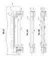
- FIG. 1is a side cross-sectional view of a pedestal and an edge coupling ring according to the prior art
- FIG. 2is a side cross-sectional view of a pedestal and an edge coupling ring according to the prior art after erosion of the edge coupling ring has occurred;
- FIG. 3is a side cross-sectional view of an example of a pedestal, an edge coupling ring and an actuator according to the present disclosure
- FIG. 4is a side cross-sectional view of the pedestal, the edge coupling ring and the actuator of FIG. 3 after erosion of the edge coupling ring has occurred;
- FIG. 5is a side cross-sectional view of the pedestal, the edge coupling ring and the actuator of FIG. 3 after erosion of the edge coupling ring has occurred and the actuator is moved;
- FIG. 6is a side cross-sectional view of another example of a pedestal, an edge coupling ring and an actuator located in another position according to the present disclosure
- FIG. 7is a side cross-sectional view of another example of a pedestal, an edge coupling ring and a piezoelectric actuator according to the present disclosure
- FIG. 8is a side cross-sectional view of the pedestal, the edge coupling ring and the piezoelectric actuator of FIG. 7 after erosion has occurred and the piezoelectric actuator is moved;
- FIG. 9is a functional block diagram of an example of a substrate processing chamber including a pedestal, an edge coupling ring and an actuator according to the present disclosure
- FIG. 10is a flowchart illustrating steps of an example of a method for operating the actuator to move the edge coupling ring according to the present disclosure
- FIG. 11is a flowchart illustrating steps of another example of a method for operating the actuator to move the edge coupling ring according to the present disclosure
- FIG. 12is a functional block diagram of an example of a processing chamber including an edge coupling ring movable by actuators arranged outside of the processing chamber according to the present disclosure
- FIG. 13A and 13Billustrates an example of side-to-side tilting of an edge coupling ring according to the present disclosure
- FIG. 14illustrates an example of a method for moving an edge coupling ring during processing of a substrate.
- the present disclosureallows one or more portions of an edge coupling ring to be moved vertically and/or horizontally relative to a substrate or pedestal in a substrate processing system.
- the movementchanges an edge coupling effect of the plasma relative to the substrate during etching or other substrate treatment without requiring the processing chamber to be opened.
- a substrate processing systemincludes a pedestal 20 and an edge coupling ring 60 .
- the edge coupling ring 60may be made of a single portion or two or more portions may be used.
- the edge coupling ring 60includes a first annular portion 72 arranged radially outside of the substrate 33 .
- a second annular portion 74is located radially inwardly from the first annular portion 72 below the substrate 33 .
- a third annular portion 76is arranged below the first annular portion 72 .
- An actuator 80may be arranged in various locations to move one or more portions of the edge coupling ring 60 relative to the substrate 33 as will be described further below.
- the actuator 80is arranged between the first annular portion 72 of the edge coupling ring 60 and the third annular portion 76 of the edge coupling ring 60 .
- the actuator 80may include a piezoelectric actuator, a stepper motor, a pneumatic drive, or other suitable actuator.
- one, two, three, or four or more actuatorsare used.
- multiple actuatorsare arranged uniformly around the edge coupling ring 60 .
- the actuator(s) 80may be arranged inside or outside of the processing chamber.
- plasma 82is directed at the substrate 33 to etch the exposed portions of the substrate 33 .
- the edge coupling ring 60is arranged to help shape the plasma electric field such that uniform etching of the substrate 33 occurs.
- one or more portions of the edge coupling ring 60may be eroded by the plasma 82 .
- non-uniform etching of the substrate 33may occur near a radially outer edge of the substrate 33 .
- the processwould need to be stopped, the processing chamber opened and the edge coupling ring replaced.
- the actuator 80is used to move one or more portions of the edge coupling ring 60 to alter the position of the one or more portions of the edge coupling ring 60 .
- the actuator 80may be used to move the first annular portion 72 of the edge coupling ring 60 .
- the actuator 80moves the first annular portion 72 of the edge coupling ring 60 in an upward or vertical direction such that an edge 86 of the first annular portion 72 of the edge coupling ring 60 is higher relative to the radially outer edge of the substrate 33 .
- etch uniformity near the radially outer edge of the substrate 33is improved.
- the actuatormay be arranged in one or more other locations and may move in other directions such as horizontal, diagonal, etc. Horizontal movement of the portion of the edge coupling ring may be performed to center the edge coupling effect relative to the substrate.
- an actuator 110is arranged radially outside of the edge coupling ring 60 .
- the actuator 110moves in a vertical (or an up/down) direction as well as in a horizontal (or side to side) direction.
- Horizontal repositioningmay be used when etching of the substrates shows a horizontal offset of the edge coupling ring relative to the substrates. The horizontal offset may be corrected without opening the processing chamber.
- tilting of the edge coupling ringmay be performed by actuating some of the actuators differently than others of the actuators to correct or create side-to-side asymmetry.
- the actuator 110may also be attached to a radially outer wall or other structure identified at 114 .
- the actuator 110may be supported from below by a wall or other structure identified at 116 .
- FIG. 7-8another example of an edge coupling ring 150 and a piezoelectric actuator 154 is shown.
- the piezoelectric actuator 154moves the edge coupling ring 150 .
- the piezoelectric actuator 154is mounted in the first annular portion 72 and the third annular portion 76 of the edge coupling ring 60 .
- the piezoelectric actuator 154moves the first annular portion 72 of the edge coupling ring 150 to adjust a position of an edge 156 of the first annular portion 72 .
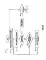
- the substrate processing chamber 500includes a processing chamber 502 that encloses other components of the substrate processing chamber 500 and contains the RF plasma.
- the substrate processing chamber 500includes an upper electrode 504 and a pedestal 506 including a lower electrode 507 .
- An edge coupling ring 503is supported by the pedestal 506 and is arranged around the substrate 508 .
- One or more actuators 505may be used to move the edge coupling ring 503 .
- a substrate 508is arranged on the pedestal 506 between the upper electrode 504 and the lower electrode 507 .
- the upper electrode 504may include a showerhead 509 that introduces and distributes process gases.
- the showerhead 509may include a stem portion including one end connected to a top surface of the processing chamber.
- a base portionis generally cylindrical and extends radially outwardly from an opposite end of the stem portion at a location that is spaced from the top surface of the processing chamber.
- a substrate-facing surface or faceplate of the base portion of the showerheadincludes a plurality of holes through which process gas or purge gas flows.
- the upper electrode 504may include a conducting plate and the process gases may be introduced in another manner.
- the lower electrode 507may be arranged in a non-conductive pedestal.
- the pedestal 506may include an electrostatic chuck that includes a conductive plate that acts as the lower electrode 507 .
- An RF generating system 510generates and outputs an RF voltage to one of the upper electrode 504 and the lower electrode 507 .
- the other one of the upper electrode 504 and the lower electrode 507may be DC grounded, AC grounded or floating.
- the RF generating system 510may include an RF voltage generator 511 that generates the RF voltage that is fed by a matching and distribution network 512 to the upper electrode 504 or the lower electrode 507 .
- the plasmamay be generated inductively or remotely.
- a gas delivery system 530includes one or more gas sources 532 - 1 , 532 - 2 , . . . , and 532 -N (collectively gas sources 532 ), where N is an integer greater than zero.
- the gas sourcessupply one or more precursors and mixtures thereof.
- the gas sourcesmay also supply purge gas. Vaporized precursor may also be used.
- the gas sources 532are connected by valves 534 - 1 , 534 - 2 , . . . , and 534 -N (collectively valves 534 ) and mass flow controllers 536 - 1 , 536 - 2 , . . .
- a manifold 540An output of the manifold 540 is fed to the processing chamber 502 .
- the output of the manifold 540is fed to the showerhead 509 .
- a heater 542may be connected to a heater coil (not shown) arranged in the pedestal 506 .
- the heater 542may be used to control a temperature of the pedestal 506 and the substrate 508 .
- a valve 550 and pump 552may be used to evacuate reactants from the processing chamber 502 .
- a controller 560may be used to control components of the substrate processing chamber 500 .
- the controller 560may also be used to control the actuator 505 to adjust a position of one or more portions of the edge coupling ring 503 .
- a robot 570 and a sensor 572may be used to measure erosion of the edge coupling ring.
- the sensor 572may include a depth gauge.
- the robot 570may move the depth gauge in contact with the edge coupling ring to measure erosion.
- a laser interferometer(with or without the robot 570 ) may be used to measure erosion without direct contact.
- the robot 570may be omitted if the laser interferometer can be positioned with a direct line of sight to the edge coupling ring.
- FIG. 10an example of a method 600 for operating the actuator to move the edge coupling ring is shown.
- 610at least part of an edge coupling ring is positioned in a first location relative to the substrate.
- the substrate processing systemis operated. The operation may include etching or other treatment of a substrate.
- controldetermines whether a predetermined period of etching or a predetermined number etching cycles have occurred. If the predetermined period or number of cycles is not exceeded as determined at 618 , control returns to 614 .
- controldetermines at 624 whether a maximum predetermined etching period is up, a maximum number of etching cycles has occurred and/or a maximum # of actuator moves have occurred.
- controlmoves at least part of the edge coupling ring using the actuator. Movement of the edge coupling ring can be performed automatically, manually or a combination thereof without opening the processing chamber. If 624 is true, control sends a message or otherwise indicates that the edge coupling ring should be serviced/replaced.
- FIG. 11an example of a method 700 for operating the actuator to move the edge coupling ring is shown.
- At 710at least part of an edge coupling ring is positioned in a first location relative to the substrate.
- the substrate processing systemis operated. The operation may include etching or other treatment of a substrate.
- controldetermines whether a predetermined amount of erosion of the edge coupling ring has occurred using a sensor such as a depth gauge or laser interferometer. If 718 is false, control returns to 714 .
- controldetermines at 724 whether a maximum amount of erosion has occurred. If 724 is false, control moves at least part of the edge coupling ring using the actuator. Movement of the edge coupling ring can be performed automatically, manually or a combination thereof without opening the processing chamber. If 724 is true, control sends a message or otherwise indicates that the edge coupling ring should be serviced/replaced.
- a determination of whether or not the edge coupling ring needs to be movedmay be based on inspection of etching patterns of the substrates after processing.
- the actuatormay be used to adjust the edge coupling profile of the edge coupling ring without opening the chamber.
- a processing chamber 800includes an edge coupling ring 60 arranged on a pedestal 20 .
- the edge coupling ring 60includes one or more portions that are movable by one or more actuators 804 arranged outside of the processing chamber 800 .
- the portion 72is movable.
- the actuators 804may be connected by mechanical linkage 810 to the portion 72 of the edge coupling ring 60 .
- the mechanical linkage 810may include a rod member.
- the mechanical linkage 810may pass through a hole 811 in a wall 814 of the processing chamber 800 .
- a seal 812such as an “O”-ring may be used.
- the mechanical linkage 810may pass through holes 815 in one or more structures such as the portion 76 of the edge coupling ring 60 .
- FIG. 13A and 13Bside-to-side tilting of an edge coupling ring 830 is shown. Side-to-side tilting may be used to correct side-to-side misalignment.
- portions 830 - 1 and 830 - 2 of an edge coupling ring 830 on opposite sides of the substrateare arranged in a first arrangement 840 .
- the portions 830 - 1 and 830 - 2may be generally aligned with portions 832 - 1 and 832 - 2 of the edge coupling ring 830 .
- Actuators 836 - 1 and 836 - 2are arranged between the portions 830 - 1 and 832 - 1 and 830 - 2 and 832 - 2 , respectively.
- the actuators 836 - 1 and 836 - 2move the respective portions of the edge coupling ring 830 such that the edge coupling ring 830 moves to a second arrangement 850 that is different than the first arrangement 840 shown in FIG. 13A .
- the substratesmay be inspected after treatment and the tilt relative to the substrate may be adjusted as needed without opening the processing chamber.
- a method 900 for moving an edge coupling ring during processing of a substrateis shown.
- different treatmentsmay be performed on a single substrate in the same processing chamber.
- the edge coupling effect of the edge coupling ringmay be adjusted between the multiple treatments performed on the substrate in the same processing chamber before proceeding to a subsequent substrate.
- a substrateis positioned on a pedestal and a position of the edge coupling ring is adjusted if needed.
- treatment of the substrateis performed. If processing of the substrate is done as determined at 918 , the substrate is moved from the pedestal at 922 .
- controldetermines whether another substrate needs to be processed. If 924 is true, the method returns to 910 . Otherwise the method ends.
- the methoddetermines whether adjustment of the edge coupling ring is required at 930 . If 930 is false, the method returns to 914 . If 930 is true, at least part of the edge coupling ring is moved using one or more actuators at 934 and the method returns to 914 . As can be appreciated, the edge coupling ring can be adjusted between treatments of the same substrate in the same processing chamber.
- a controlleris part of a system, which may be part of the above-described examples.
- Such systemscan comprise semiconductor processing equipment, including a processing tool or tools, chamber or chambers, a platform or platforms for processing, and/or specific processing components (a wafer pedestal, a gas flow system, etc.).
- These systemsmay be integrated with electronics for controlling their operation before, during, and after processing of a semiconductor wafer or substrate.
- the electronicsmay be referred to as the “controller,” which may control various components or subparts of the system or systems.
- the controllermay be programmed to control any of the processes disclosed herein, including the delivery of processing gases, temperature settings (e.g., heating and/or cooling), pressure settings, vacuum settings, power settings, radio frequency (RF) generator settings, RF matching circuit settings, frequency settings, flow rate settings, fluid delivery settings, positional and operation settings, wafer transfers into and out of a tool and other transfer tools and/or load locks connected to or interfaced with a specific system.
- temperature settingse.g., heating and/or cooling
- RFradio frequency
- the controllermay be defined as electronics having various integrated circuits, logic, memory, and/or software that receive instructions, issue instructions, control operation, enable cleaning operations, enable endpoint measurements, and the like.
- the integrated circuitsmay include chips in the form of firmware that store program instructions, digital signal processors (DSPs), chips defined as application specific integrated circuits (ASICs), and/or one or more microprocessors, or microcontrollers that execute program instructions (e.g., software).
- Program instructionsmay be instructions communicated to the controller in the form of various individual settings (or program files), defining operational parameters for carrying out a particular process on or for a semiconductor wafer or to a system.
- the operational parametersmay, in some embodiments, be part of a recipe defined by process engineers to accomplish one or more processing steps during the fabrication of one or more layers, materials, metals, oxides, silicon, silicon dioxide, surfaces, circuits, and/or dies of a wafer.
- the controllermay be a part of or coupled to a computer that is integrated with the system, coupled to the system, otherwise networked to the system, or a combination thereof.
- the controllermay be in the “cloud” or all or a part of a fab host computer system, which can allow for remote access of the wafer processing.
- the computermay enable remote access to the system to monitor current progress of fabrication operations, examine a history of past fabrication operations, examine trends or performance metrics from a plurality of fabrication operations, to change parameters of current processing, to set processing steps to follow a current processing, or to start a new process.
- a remote computere.g. a server
- the remote computermay include a user interface that enables entry or programming of parameters and/or settings, which are then communicated to the system from the remote computer.
- the controllerreceives instructions in the form of data, which specify parameters for each of the processing steps to be performed during one or more operations. It should be understood that the parameters may be specific to the type of process to be performed and the type of tool that the controller is configured to interface with or control.
- the controllermay be distributed, such as by comprising one or more discrete controllers that are networked together and working towards a common purpose, such as the processes and controls described herein.
- An example of a distributed controller for such purposeswould be one or more integrated circuits on a chamber in communication with one or more integrated circuits located remotely (such as at the platform level or as part of a remote computer) that combine to control a process on the chamber.
- example systemsmay include a plasma etch chamber or module, a deposition chamber or module, a spin-rinse chamber or module, a metal plating chamber or module, a clean chamber or module, a bevel edge etch chamber or module, a physical vapor deposition (PVD) chamber or module, a chemical vapor deposition (CVD) chamber or module, an atomic layer deposition (ALD) chamber or module, an atomic layer etch (ALE) chamber or module, an ion implantation chamber or module, a track chamber or module, and any other semiconductor processing systems that may be associated or used in the fabrication and/or manufacturing of semiconductor wafers.
- PVDphysical vapor deposition
- CVDchemical vapor deposition
- ALDatomic layer deposition
- ALEatomic layer etch
- the controllermight communicate with one or more of other tool circuits or modules, other tool components, cluster tools, other tool interfaces, adjacent tools, neighboring tools, tools located throughout a factory, a main computer, another controller, or tools used in material transport that bring containers of wafers to and from tool locations and/or load ports in a semiconductor manufacturing factory.
Landscapes
- Engineering & Computer Science (AREA)
- Physics & Mathematics (AREA)
- Power Engineering (AREA)
- Condensed Matter Physics & Semiconductors (AREA)
- General Physics & Mathematics (AREA)
- Manufacturing & Machinery (AREA)
- Computer Hardware Design (AREA)
- Microelectronics & Electronic Packaging (AREA)
- Chemical & Material Sciences (AREA)
- Plasma & Fusion (AREA)
- Analytical Chemistry (AREA)
- Container, Conveyance, Adherence, Positioning, Of Wafer (AREA)
- Chemical Kinetics & Catalysis (AREA)
- General Chemical & Material Sciences (AREA)
- Inorganic Chemistry (AREA)
- Drying Of Semiconductors (AREA)
Abstract
Description
- The present disclosure relates to substrate processing systems, and more particularly to edge coupling rings of substrate processing systems.
- The background description provided here is for the purpose of generally presenting the context of the disclosure. Work of the presently named inventors, to the extent it is described in this background section, as well as aspects of the description that may not otherwise qualify as prior art at the time of filing, are neither expressly nor impliedly admitted as prior art against the present disclosure.
- Substrate processing systems may be used to perform etching and/or other treatment of substrates such as semiconductor wafers. A substrate may be arranged on a pedestal in a processing chamber of the substrate processing system. For example during etching in a plasma enhanced chemical vapor deposition (PECVD) process, a gas mixture including one or more precursors is introduced into the processing chamber and plasma is struck to etch the substrate.
- Edge coupling rings have been used to adjust an etch rate and/or etch profile of the plasma near a radially outer edge of the substrate. The edge coupling ring is typically located on the pedestal around the radially outer edge of the substrate. Process conditions at the radially outer edge of the substrate can be modified by changing a position of the edge coupling ring, a shape or profile of an inner edge of the edge coupling ring, a height of the edge coupling ring relative to an upper surface of the substrate, a material of the edge coupling ring, etc.
- Changing the edge coupling ring requires the processing chamber to be opened, which is undesirable. In other words, an edge coupling effect of the edge coupling ring cannot be altered without opening the processing chamber. When the edge coupling ring is eroded by plasma during etching, the edge coupling effect changes. Correcting erosion of the edge coupling ring requires the processing chamber to be opened in order to replace the edge coupling ring.
- Referring now to
FIGS. 1-2 , a substrate processing system may include apedestal 20 and anedge coupling ring 30. Theedge coupling ring 30 may include a single piece or two or more portions. In the example inFIGS. 1-2 , theedge coupling ring 30 includes a firstannular portion 32 arranged near a radially outer edge of asubstrate 33. A secondannular portion 34 is located radially inwardly from the first annular portion below thesubstrate 33. A thirdannular portion 36 is arranged below the firstannular portion 32. During use,plasma 42 is directed at thesubstrate 33 to etch the exposed portions of thesubstrate 33. Theedge coupling ring 30 is arranged to help shape the plasma such that uniform etching of thesubstrate 33 occurs. - In
FIG. 2 , after theedge coupling ring 30 has been used, an upper surface of a radially inner portion of theedge coupling ring 30 may exhibit erosion as identified at48. As a result,plasma 42 may tend to etch a radially outer edge of thesubstrate 33 at a faster rate than etching of radially inner portions thereof as can be seen at44. - A substrate processing system includes a processing chamber. A pedestal is arranged in the processing chamber. An edge coupling ring is arranged adjacent to the pedestal and around a radially outer edge of the substrate. An actuator is configured to selectively move a first portion of the edge coupling ring relative to the substrate to alter an edge coupling profile of the edge coupling ring.
- In other features, a gas delivery system is configured to deliver process gas and carrier gas to the processing chamber. A plasma generator is configured to create plasma in the processing chamber to etch the substrate. The actuator moves the first portion of the edge coupling ring without requiring the processing chamber to be opened.
- In other features, the edge coupling ring further comprises a second portion. The actuator is configured to move the first portion of the edge coupling ring relative the second portion of the edge coupling ring. The actuator includes a piezoelectric actuator. The actuator includes a stepper motor actuator. The actuator includes a pneumatic drive actuator.
- In other features, a controller is configured to move the edge coupling ring in response to erosion of a plasma-facing surface of the edge coupling ring. The controller automatically moves the edge coupling ring after the edge coupling ring is exposed to a predetermined number of etching cycles. The controller automatically moves the edge coupling ring after the edge coupling ring is exposed to a predetermined period of etching.
- In other features, the actuator moves the first portion of the edge coupling ring vertically relative to the substrate. The actuator moves the first portion of the edge coupling ring horizontally relative to the substrate. A sensor is configured to communicate with the controller and to detect the erosion of the edge coupling ring.
- In other features, a robot is configured to communicate with the controller and to adjust a position of the sensor. The sensor includes a depth gauge. The sensor includes a laser interferometer. The actuator selectively tilts the edge coupling ring relative to the substrate. The actuator is located outside of the processing chamber. A rod member connects the actuator to the edge coupling ring through a wall of the processing chamber.
- In other features, a seal is arranged between the rod member and the wall of the processing chamber. A controller is configured to move the edge coupling ring to a first position for a first treatment of the substrate using a first edge coupling effect and then to a second position for a second treatment of the substrate using a second edge coupling effect.
- A method for adjusting an edge coupling profile of an edge coupling ring in a substrate processing system includes arranging an edge coupling ring adjacent to a pedestal in a processing chamber. The edge coupling ring is arranged around a radially outer edge of the substrate. The method includes selectively moving a first portion of the edge coupling ring relative to the substrate using an actuator to alter an edge coupling profile of the edge coupling ring.
- In other features, the method includes delivering process gas and carrier gas to the processing chamber. The method includes creating plasma in the processing chamber to etch the substrate. The method includes moving the first portion of the edge coupling ring using the actuator without requiring the processing chamber to be opened. The edge coupling ring further comprises a second portion. The actuator is configured to move the first portion of the edge coupling ring relative the second portion of the edge coupling ring. The actuator is selected from a group consisting of a piezoelectric actuator, a stepper motor actuator, and a pneumatic drive actuator.
- In other features, the method includes moving the edge coupling ring in response to erosion of a plasma-facing surface of the edge coupling ring. The method includes automatically moving the edge coupling ring after the edge coupling ring is exposed to a predetermined number of etching cycles. The method includes automatically moving the edge coupling ring after the edge coupling ring is exposed to a predetermined period of etching. The method includes moving the first portion of the edge coupling ring vertically relative to the substrate. The method includes moving the first portion of the edge coupling ring horizontally relative to the substrate.
- In other features, the method includes using a sensor to sense erosion of the edge coupling ring. The sensor is selected from a group consisting of a depth gauge and a laser interferometer. The method includes selectively tilting the edge coupling ring relative to the substrate. The actuator is located outside of the processing chamber.
- In other features, the method includes moving the edge coupling ring to a first position for a first treatment of the substrate using a first edge coupling effect and moving the edge coupling ring to a second position for a second treatment of the substrate using a second edge coupling effect.
- Further areas of applicability of the present disclosure will become apparent from the detailed description, the claims and the drawings. The detailed description and specific examples are intended for purposes of illustration only and are not intended to limit the scope of the disclosure.
- The present disclosure will become more fully understood from the detailed description and the accompanying drawings, wherein:
FIG. 1 is a side cross-sectional view of a pedestal and an edge coupling ring according to the prior art;FIG. 2 is a side cross-sectional view of a pedestal and an edge coupling ring according to the prior art after erosion of the edge coupling ring has occurred;FIG. 3 is a side cross-sectional view of an example of a pedestal, an edge coupling ring and an actuator according to the present disclosure;FIG. 4 is a side cross-sectional view of the pedestal, the edge coupling ring and the actuator ofFIG. 3 after erosion of the edge coupling ring has occurred;FIG. 5 is a side cross-sectional view of the pedestal, the edge coupling ring and the actuator ofFIG. 3 after erosion of the edge coupling ring has occurred and the actuator is moved;FIG. 6 is a side cross-sectional view of another example of a pedestal, an edge coupling ring and an actuator located in another position according to the present disclosure;FIG. 7 is a side cross-sectional view of another example of a pedestal, an edge coupling ring and a piezoelectric actuator according to the present disclosure;FIG. 8 is a side cross-sectional view of the pedestal, the edge coupling ring and the piezoelectric actuator ofFIG. 7 after erosion has occurred and the piezoelectric actuator is moved;FIG. 9 is a functional block diagram of an example of a substrate processing chamber including a pedestal, an edge coupling ring and an actuator according to the present disclosure;FIG. 10 is a flowchart illustrating steps of an example of a method for operating the actuator to move the edge coupling ring according to the present disclosure;FIG. 11 is a flowchart illustrating steps of another example of a method for operating the actuator to move the edge coupling ring according to the present disclosure;FIG. 12 is a functional block diagram of an example of a processing chamber including an edge coupling ring movable by actuators arranged outside of the processing chamber according to the present disclosure;FIG. 13A and 13B illustrates an example of side-to-side tilting of an edge coupling ring according to the present disclosure; andFIG. 14 illustrates an example of a method for moving an edge coupling ring during processing of a substrate.- In the drawings, reference numbers may be reused to identify similar and/or identical elements.
- The present disclosure allows one or more portions of an edge coupling ring to be moved vertically and/or horizontally relative to a substrate or pedestal in a substrate processing system. The movement changes an edge coupling effect of the plasma relative to the substrate during etching or other substrate treatment without requiring the processing chamber to be opened.
- Referring now to
FIGS. 3-5 , a substrate processing system includes apedestal 20 and anedge coupling ring 60. Theedge coupling ring 60 may be made of a single portion or two or more portions may be used. In the example inFIGS. 3-5 , theedge coupling ring 60 includes a firstannular portion 72 arranged radially outside of thesubstrate 33. A secondannular portion 74 is located radially inwardly from the firstannular portion 72 below thesubstrate 33. A thirdannular portion 76 is arranged below the firstannular portion 72. - An
actuator 80 may be arranged in various locations to move one or more portions of theedge coupling ring 60 relative to thesubstrate 33 as will be described further below. For example only, inFIG. 3 theactuator 80 is arranged between the firstannular portion 72 of theedge coupling ring 60 and the thirdannular portion 76 of theedge coupling ring 60. In some examples, theactuator 80 may include a piezoelectric actuator, a stepper motor, a pneumatic drive, or other suitable actuator. In some examples, one, two, three, or four or more actuators are used. In some examples, multiple actuators are arranged uniformly around theedge coupling ring 60. The actuator(s)80 may be arranged inside or outside of the processing chamber. - During use,
plasma 82 is directed at thesubstrate 33 to etch the exposed portions of thesubstrate 33. Theedge coupling ring 60 is arranged to help shape the plasma electric field such that uniform etching of thesubstrate 33 occurs. As can be seen at84 and86 inFIG. 4 , one or more portions of theedge coupling ring 60 may be eroded by theplasma 82. As a result of the erosion, non-uniform etching of thesubstrate 33 may occur near a radially outer edge of thesubstrate 33. Normally, the process would need to be stopped, the processing chamber opened and the edge coupling ring replaced. - In
FIG. 5 , theactuator 80 is used to move one or more portions of theedge coupling ring 60 to alter the position of the one or more portions of theedge coupling ring 60. For example, theactuator 80 may be used to move the firstannular portion 72 of theedge coupling ring 60. In this example, theactuator 80 moves the firstannular portion 72 of theedge coupling ring 60 in an upward or vertical direction such that anedge 86 of the firstannular portion 72 of theedge coupling ring 60 is higher relative to the radially outer edge of thesubstrate 33. As a result, etch uniformity near the radially outer edge of thesubstrate 33 is improved. - Referring now to
FIG. 6 , as can be appreciated, the actuator may be arranged in one or more other locations and may move in other directions such as horizontal, diagonal, etc. Horizontal movement of the portion of the edge coupling ring may be performed to center the edge coupling effect relative to the substrate. InFIG. 6 , anactuator 110 is arranged radially outside of theedge coupling ring 60. In addition, theactuator 110 moves in a vertical (or an up/down) direction as well as in a horizontal (or side to side) direction. Horizontal repositioning may be used when etching of the substrates shows a horizontal offset of the edge coupling ring relative to the substrates. The horizontal offset may be corrected without opening the processing chamber. Likewise, tilting of the edge coupling ring may be performed by actuating some of the actuators differently than others of the actuators to correct or create side-to-side asymmetry. - Rather than locating the
actuator 110 between annular portions of the edge coupling ring, theactuator 110 may also be attached to a radially outer wall or other structure identified at114. Alternately, theactuator 110 may be supported from below by a wall or other structure identified at116. - Referring now to
FIG. 7-8 , another example of anedge coupling ring 150 and apiezoelectric actuator 154 is shown. In this example, thepiezoelectric actuator 154 moves theedge coupling ring 150. Thepiezoelectric actuator 154 is mounted in the firstannular portion 72 and the thirdannular portion 76 of theedge coupling ring 60. InFIG. 8 , thepiezoelectric actuator 154 moves the firstannular portion 72 of theedge coupling ring 150 to adjust a position of anedge 156 of the firstannular portion 72. - Referring now to
FIG. 9 , an example of asubstrate processing chamber 500 for performing etching using RF plasma is shown. Thesubstrate processing chamber 500 includes aprocessing chamber 502 that encloses other components of thesubstrate processing chamber 500 and contains the RF plasma. Thesubstrate processing chamber 500 includes anupper electrode 504 and apedestal 506 including alower electrode 507. Anedge coupling ring 503 is supported by thepedestal 506 and is arranged around thesubstrate 508. One ormore actuators 505 may be used to move theedge coupling ring 503. During operation, asubstrate 508 is arranged on thepedestal 506 between theupper electrode 504 and thelower electrode 507. - For example only, the
upper electrode 504 may include ashowerhead 509 that introduces and distributes process gases. Theshowerhead 509 may include a stem portion including one end connected to a top surface of the processing chamber. A base portion is generally cylindrical and extends radially outwardly from an opposite end of the stem portion at a location that is spaced from the top surface of the processing chamber. A substrate-facing surface or faceplate of the base portion of the showerhead includes a plurality of holes through which process gas or purge gas flows. Alternately, theupper electrode 504 may include a conducting plate and the process gases may be introduced in another manner. Thelower electrode 507 may be arranged in a non-conductive pedestal. Alternately, thepedestal 506 may include an electrostatic chuck that includes a conductive plate that acts as thelower electrode 507. - An
RF generating system 510 generates and outputs an RF voltage to one of theupper electrode 504 and thelower electrode 507. The other one of theupper electrode 504 and thelower electrode 507 may be DC grounded, AC grounded or floating. For example only, theRF generating system 510 may include an RF voltage generator511 that generates the RF voltage that is fed by a matching anddistribution network 512 to theupper electrode 504 or thelower electrode 507. In other examples, the plasma may be generated inductively or remotely. - A
gas delivery system 530 includes one or more gas sources532-1,532-2, . . . , and532-N (collectively gas sources532), where N is an integer greater than zero. The gas sources supply one or more precursors and mixtures thereof. The gas sources may also supply purge gas. Vaporized precursor may also be used. Thegas sources 532 are connected by valves534-1,534-2, . . . , and534-N (collectively valves534) and mass flow controllers536-1,536-2, . . . , and536-N (collectively mass flow controllers536) to amanifold 540. An output of the manifold540 is fed to theprocessing chamber 502. For example only, the output of the manifold540 is fed to theshowerhead 509. - A
heater 542 may be connected to a heater coil (not shown) arranged in thepedestal 506. Theheater 542 may be used to control a temperature of thepedestal 506 and thesubstrate 508. Avalve 550 and pump552 may be used to evacuate reactants from theprocessing chamber 502. Acontroller 560 may be used to control components of thesubstrate processing chamber 500. Thecontroller 560 may also be used to control theactuator 505 to adjust a position of one or more portions of theedge coupling ring 503. - A
robot 570 and asensor 572 may be used to measure erosion of the edge coupling ring. In some examples, thesensor 572 may include a depth gauge. Therobot 570 may move the depth gauge in contact with the edge coupling ring to measure erosion. Alternately, a laser interferometer (with or without the robot570) may be used to measure erosion without direct contact. Therobot 570 may be omitted if the laser interferometer can be positioned with a direct line of sight to the edge coupling ring. - Referring now to
FIG. 10 , an example of amethod 600 for operating the actuator to move the edge coupling ring is shown. At610, at least part of an edge coupling ring is positioned in a first location relative to the substrate. At614, the substrate processing system is operated. The operation may include etching or other treatment of a substrate. At618, control determines whether a predetermined period of etching or a predetermined number etching cycles have occurred. If the predetermined period or number of cycles is not exceeded as determined at618, control returns to614. - When the predetermined period or number of cycles are up, control determines at624 whether a maximum predetermined etching period is up, a maximum number of etching cycles has occurred and/or a maximum # of actuator moves have occurred.
- If624 is false, control moves at least part of the edge coupling ring using the actuator. Movement of the edge coupling ring can be performed automatically, manually or a combination thereof without opening the processing chamber. If624 is true, control sends a message or otherwise indicates that the edge coupling ring should be serviced/replaced.
- Referring now to
FIG. 11 , an example of amethod 700 for operating the actuator to move the edge coupling ring is shown. At710, at least part of an edge coupling ring is positioned in a first location relative to the substrate. At714, the substrate processing system is operated. The operation may include etching or other treatment of a substrate. At718, control determines whether a predetermined amount of erosion of the edge coupling ring has occurred using a sensor such as a depth gauge or laser interferometer. If718 is false, control returns to714. - When the predetermined amount of erosion has occurred, control determines at724 whether a maximum amount of erosion has occurred. If724 is false, control moves at least part of the edge coupling ring using the actuator. Movement of the edge coupling ring can be performed automatically, manually or a combination thereof without opening the processing chamber. If724 is true, control sends a message or otherwise indicates that the edge coupling ring should be serviced/replaced.
- In addition to the foregoing, a determination of whether or not the edge coupling ring needs to be moved may be based on inspection of etching patterns of the substrates after processing. The actuator may be used to adjust the edge coupling profile of the edge coupling ring without opening the chamber.
- Referring now to
FIG. 12 , aprocessing chamber 800 includes anedge coupling ring 60 arranged on apedestal 20. Theedge coupling ring 60 includes one or more portions that are movable by one ormore actuators 804 arranged outside of theprocessing chamber 800. In this example, theportion 72 is movable. Theactuators 804 may be connected bymechanical linkage 810 to theportion 72 of theedge coupling ring 60. For example, themechanical linkage 810 may include a rod member. Themechanical linkage 810 may pass through ahole 811 in awall 814 of theprocessing chamber 800. Aseal 812 such as an “O”-ring may be used. Themechanical linkage 810 may pass throughholes 815 in one or more structures such as theportion 76 of theedge coupling ring 60. - Referring now to
FIG. 13A and 13B , side-to-side tilting of anedge coupling ring 830 is shown. Side-to-side tilting may be used to correct side-to-side misalignment. InFIG. 13A , portions830-1 and830-2 of anedge coupling ring 830 on opposite sides of the substrate are arranged in afirst arrangement 840. The portions830-1 and830-2 may be generally aligned with portions832-1 and832-2 of theedge coupling ring 830. Actuators836-1 and836-2 are arranged between the portions830-1 and832-1 and830-2 and832-2, respectively. - In
FIG. 13B , the actuators836-1 and836-2 move the respective portions of theedge coupling ring 830 such that theedge coupling ring 830 moves to asecond arrangement 850 that is different than thefirst arrangement 840 shown inFIG. 13A . As can be appreciated, the substrates may be inspected after treatment and the tilt relative to the substrate may be adjusted as needed without opening the processing chamber. - Referring now to
FIG. 14 , amethod 900 for moving an edge coupling ring during processing of a substrate is shown. In other words, different treatments may be performed on a single substrate in the same processing chamber. The edge coupling effect of the edge coupling ring may be adjusted between the multiple treatments performed on the substrate in the same processing chamber before proceeding to a subsequent substrate. At910, a substrate is positioned on a pedestal and a position of the edge coupling ring is adjusted if needed. At914, treatment of the substrate is performed. If processing of the substrate is done as determined at918, the substrate is moved from the pedestal at922. At924, control determines whether another substrate needs to be processed. If924 is true, the method returns to910. Otherwise the method ends. - If918 is false and the substrate needs additional treatment, the method determines whether adjustment of the edge coupling ring is required at930. If930 is false, the method returns to914. If930 is true, at least part of the edge coupling ring is moved using one or more actuators at934 and the method returns to914. As can be appreciated, the edge coupling ring can be adjusted between treatments of the same substrate in the same processing chamber.
- The foregoing description is. merely illustrative in nature and is in no way intended to limit the disclosure, its application, or uses. The broad teachings of the disclosure can be implemented in a variety of forms. Therefore, while this disclosure includes particular examples, the true scope of the disclosure should not be so limited since other modifications will become apparent upon a study of the drawings, the specification, and the following claims. As used herein, the phrase at least one of A, B, and C should be construed to mean a logical (A OR B OR C), using a non-exclusive. logical OR, and should not be construed to mean “at least one of A, at least one of B, and at least one of C.” It should be understood that one or more steps within a method may be executed in different order (or concurrently) without altering the principles of the present disclosure.
- In some implementations, a controller is part of a system, which may be part of the above-described examples. Such systems can comprise semiconductor processing equipment, including a processing tool or tools, chamber or chambers, a platform or platforms for processing, and/or specific processing components (a wafer pedestal, a gas flow system, etc.). These systems may be integrated with electronics for controlling their operation before, during, and after processing of a semiconductor wafer or substrate. The electronics may be referred to as the “controller,” which may control various components or subparts of the system or systems. The controller, depending on the processing requirements and/or the type of system, may be programmed to control any of the processes disclosed herein, including the delivery of processing gases, temperature settings (e.g., heating and/or cooling), pressure settings, vacuum settings, power settings, radio frequency (RF) generator settings, RF matching circuit settings, frequency settings, flow rate settings, fluid delivery settings, positional and operation settings, wafer transfers into and out of a tool and other transfer tools and/or load locks connected to or interfaced with a specific system.
- Broadly speaking, the controller may be defined as electronics having various integrated circuits, logic, memory, and/or software that receive instructions, issue instructions, control operation, enable cleaning operations, enable endpoint measurements, and the like. The integrated circuits may include chips in the form of firmware that store program instructions, digital signal processors (DSPs), chips defined as application specific integrated circuits (ASICs), and/or one or more microprocessors, or microcontrollers that execute program instructions (e.g., software). Program instructions may be instructions communicated to the controller in the form of various individual settings (or program files), defining operational parameters for carrying out a particular process on or for a semiconductor wafer or to a system. The operational parameters may, in some embodiments, be part of a recipe defined by process engineers to accomplish one or more processing steps during the fabrication of one or more layers, materials, metals, oxides, silicon, silicon dioxide, surfaces, circuits, and/or dies of a wafer.
- The controller, in some implementations, may be a part of or coupled to a computer that is integrated with the system, coupled to the system, otherwise networked to the system, or a combination thereof. For example, the controller may be in the “cloud” or all or a part of a fab host computer system, which can allow for remote access of the wafer processing. The computer may enable remote access to the system to monitor current progress of fabrication operations, examine a history of past fabrication operations, examine trends or performance metrics from a plurality of fabrication operations, to change parameters of current processing, to set processing steps to follow a current processing, or to start a new process. In some examples, a remote computer (e.g. a server) can provide process recipes to a system over a network, which may include a local network or the Internet. The remote computer may include a user interface that enables entry or programming of parameters and/or settings, which are then communicated to the system from the remote computer. In some examples, the controller receives instructions in the form of data, which specify parameters for each of the processing steps to be performed during one or more operations. It should be understood that the parameters may be specific to the type of process to be performed and the type of tool that the controller is configured to interface with or control. Thus as described above, the controller may be distributed, such as by comprising one or more discrete controllers that are networked together and working towards a common purpose, such as the processes and controls described herein. An example of a distributed controller for such purposes would be one or more integrated circuits on a chamber in communication with one or more integrated circuits located remotely (such as at the platform level or as part of a remote computer) that combine to control a process on the chamber.
- Without limitation, example systems may include a plasma etch chamber or module, a deposition chamber or module, a spin-rinse chamber or module, a metal plating chamber or module, a clean chamber or module, a bevel edge etch chamber or module, a physical vapor deposition (PVD) chamber or module, a chemical vapor deposition (CVD) chamber or module, an atomic layer deposition (ALD) chamber or module, an atomic layer etch (ALE) chamber or module, an ion implantation chamber or module, a track chamber or module, and any other semiconductor processing systems that may be associated or used in the fabrication and/or manufacturing of semiconductor wafers.
- As noted above, depending on the process step or steps to be performed by the tool, the controller might communicate with one or more of other tool circuits or modules, other tool components, cluster tools, other tool interfaces, adjacent tools, neighboring tools, tools located throughout a factory, a main computer, another controller, or tools used in material transport that bring containers of wafers to and from tool locations and/or load ports in a semiconductor manufacturing factory.
Claims (18)
Priority Applications (21)
| Application Number | Priority Date | Filing Date | Title |
|---|---|---|---|
| US14/598,943US11605546B2 (en) | 2015-01-16 | 2015-01-16 | Moveable edge coupling ring for edge process control during semiconductor wafer processing |
| US14/705,430US10658222B2 (en) | 2015-01-16 | 2015-05-06 | Moveable edge coupling ring for edge process control during semiconductor wafer processing |
| JP2016004302AJP6783521B2 (en) | 2015-01-16 | 2016-01-13 | Movable edge coupling ring for edge processing control during semiconductor wafer processing |
| KR1020160004905AKR102537053B1 (en) | 2015-01-16 | 2016-01-14 | Moveable edge coupling ring for edge process control during semiconductor wafer processing |
| SG10201906516XASG10201906516XA (en) | 2015-01-16 | 2016-01-15 | Moveable edge coupling ring for edge process control during semiconductor wafer processing |
| SG10201600319VASG10201600319VA (en) | 2015-01-16 | 2016-01-15 | Moveable edge coupling ring for edge process control during semiconductor wafer processing |
| SG10201808035YASG10201808035YA (en) | 2015-01-16 | 2016-01-15 | Moveable edge coupling ring for edge process control during semiconductor wafer processing |
| TW105101160ATWI704645B (en) | 2015-01-16 | 2016-01-15 | Moveable edge coupling ring for edge process control during semiconductor wafer processing |
| TW107134225ATWI717638B (en) | 2015-01-16 | 2016-01-15 | Moveable edge coupling ring for edge process control during semiconductor wafer processing |
| TW109146436ATWI766510B (en) | 2015-01-16 | 2016-01-15 | Moveable edge coupling ring for edge process control during semiconductor wafer processing |
| CN201811243095.4ACN110010432A (en) | 2015-01-16 | 2016-01-18 | A kind of edge ring |
| CN201610032252.1ACN105810609B (en) | 2015-01-16 | 2016-01-18 | Movable edge coupling ring to control edge processing during semiconductor wafer processing |
| US15/609,570US20170263478A1 (en) | 2015-01-16 | 2017-05-31 | Detection System for Tunable/Replaceable Edge Coupling Ring |
| US16/131,822US20190013232A1 (en) | 2015-01-16 | 2018-09-14 | Moveable edge ring design |
| KR1020180114808AKR20180110653A (en) | 2015-01-16 | 2018-09-27 | Moveable edge coupling ring for edge process control during semiconductor wafer processing |
| JP2018186353AJP6863941B2 (en) | 2015-01-16 | 2018-10-01 | Movable edge coupling ring for edge processing control during semiconductor wafer processing |
| JP2021005504AJP2021073705A (en) | 2015-01-16 | 2021-01-18 | Movable edge coupling ring for edge processing control during semiconductor wafer processing |
| US17/181,571US12027410B2 (en) | 2015-01-16 | 2021-02-22 | Edge ring arrangement with moveable edge rings |
| KR1020210079769AKR20210080300A (en) | 2015-01-16 | 2021-06-21 | Moveable edge coupling ring for edge process control during semiconductor wafer processing |
| KR1020230128782AKR20230144988A (en) | 2015-01-16 | 2023-09-26 | Moveable edge coupling ring for edge process control during semiconductor wafer processing |
| US18/758,576US20240355667A1 (en) | 2015-01-16 | 2024-06-28 | Edge ring arrangement with moveable edge rings |
Applications Claiming Priority (1)
| Application Number | Priority Date | Filing Date | Title |
|---|---|---|---|
| US14/598,943US11605546B2 (en) | 2015-01-16 | 2015-01-16 | Moveable edge coupling ring for edge process control during semiconductor wafer processing |
Related Child Applications (1)
| Application Number | Title | Priority Date | Filing Date |
|---|---|---|---|
| US14/705,430Continuation-In-PartUS10658222B2 (en) | 2015-01-16 | 2015-05-06 | Moveable edge coupling ring for edge process control during semiconductor wafer processing |
Publications (2)
| Publication Number | Publication Date |
|---|---|
| US20160211165A1true US20160211165A1 (en) | 2016-07-21 |
| US11605546B2 US11605546B2 (en) | 2023-03-14 |
Family
ID=56408376
Family Applications (1)
| Application Number | Title | Priority Date | Filing Date |
|---|---|---|---|
| US14/598,943Active2036-07-23US11605546B2 (en) | 2015-01-16 | 2015-01-16 | Moveable edge coupling ring for edge process control during semiconductor wafer processing |
Country Status (1)
| Country | Link |
|---|---|
| US (1) | US11605546B2 (en) |
Cited By (47)
| Publication number | Priority date | Publication date | Assignee | Title |
|---|---|---|---|---|
| US9947517B1 (en) | 2016-12-16 | 2018-04-17 | Applied Materials, Inc. | Adjustable extended electrode for edge uniformity control |
| US10017857B2 (en) | 2015-05-02 | 2018-07-10 | Applied Materials, Inc. | Method and apparatus for controlling plasma near the edge of a substrate |
| CN108345178A (en)* | 2017-01-25 | 2018-07-31 | 上海微电子装备(集团)股份有限公司 | A kind of silicon chip edge protection device |
| CN109659216A (en)* | 2017-10-11 | 2019-04-19 | 东京毅力科创株式会社 | Plasma processing apparatus, the lift control method of focusing ring and program |
| US10312121B2 (en) | 2016-03-29 | 2019-06-04 | Lam Research Corporation | Systems and methods for aligning measurement device in substrate processing systems |
| US10410832B2 (en)* | 2016-08-19 | 2019-09-10 | Lam Research Corporation | Control of on-wafer CD uniformity with movable edge ring and gas injection adjustment |
| US10438833B2 (en) | 2016-02-16 | 2019-10-08 | Lam Research Corporation | Wafer lift ring system for wafer transfer |
| CN110504202A (en)* | 2018-05-17 | 2019-11-26 | 细美事有限公司 | Transmission unit and substrate board treatment including the transmission unit |
| US10553404B2 (en) | 2017-02-01 | 2020-02-04 | Applied Materials, Inc. | Adjustable extended electrode for edge uniformity control |
| US10600623B2 (en) | 2018-05-28 | 2020-03-24 | Applied Materials, Inc. | Process kit with adjustable tuning ring for edge uniformity control |
| US10651015B2 (en) | 2016-02-12 | 2020-05-12 | Lam Research Corporation | Variable depth edge ring for etch uniformity control |
| US10665490B2 (en) | 2018-07-04 | 2020-05-26 | Samsung Electronics Co., Ltd. | Apparatus and methods for edge ring replacement, inspection and alignment using image sensors |
| US10699878B2 (en) | 2016-02-12 | 2020-06-30 | Lam Research Corporation | Chamber member of a plasma source and pedestal with radially outward positioned lift pins for translation of a substrate c-ring |
| US10825659B2 (en) | 2016-01-07 | 2020-11-03 | Lam Research Corporation | Substrate processing chamber including multiple gas injection points and dual injector |
| US20210043495A1 (en)* | 2019-08-05 | 2021-02-11 | Kioxia Corporation | Plasma processing device and plasma processing method |
| US10957561B2 (en) | 2015-07-30 | 2021-03-23 | Lam Research Corporation | Gas delivery system |
| US10964584B2 (en) | 2019-05-20 | 2021-03-30 | Applied Materials, Inc. | Process kit ring adaptor |
| US11011353B2 (en) | 2016-03-29 | 2021-05-18 | Lam Research Corporation | Systems and methods for performing edge ring characterization |
| US11043400B2 (en) | 2017-12-21 | 2021-06-22 | Applied Materials, Inc. | Movable and removable process kit |
| US11075105B2 (en) | 2017-09-21 | 2021-07-27 | Applied Materials, Inc. | In-situ apparatus for semiconductor process module |
| US11098406B2 (en) | 2018-01-04 | 2021-08-24 | Samsung Electronics Co., Ltd. | Substrate support unit and deposition apparatus including the same |
| US11101115B2 (en) | 2019-04-19 | 2021-08-24 | Applied Materials, Inc. | Ring removal from processing chamber |
| US11211269B2 (en) | 2019-07-19 | 2021-12-28 | Applied Materials, Inc. | Multi-object capable loadlock system |
| US11279032B2 (en) | 2019-04-11 | 2022-03-22 | Applied Materials, Inc. | Apparatus, systems, and methods for improved joint coordinate teaching accuracy of robots |
| US11289310B2 (en) | 2018-11-21 | 2022-03-29 | Applied Materials, Inc. | Circuits for edge ring control in shaped DC pulsed plasma process device |
| USD954769S1 (en) | 2020-06-02 | 2022-06-14 | Applied Materials, Inc. | Enclosure system shelf |
| US11370114B2 (en) | 2019-12-09 | 2022-06-28 | Applied Materials, Inc. | Autoteach enclosure system |
| US11393710B2 (en) | 2016-01-26 | 2022-07-19 | Applied Materials, Inc. | Wafer edge ring lifting solution |
| US11443923B2 (en)* | 2019-09-25 | 2022-09-13 | Taiwan Semiconductor Manufacturing Company Ltd. | Apparatus for fabricating a semiconductor structure and method of fabricating a semiconductor structure |
| US20220384223A1 (en)* | 2021-05-27 | 2022-12-01 | Tokyo Electron Limited | Board processing equipment and recovery processing method |
| US20230009579A1 (en)* | 2019-12-19 | 2023-01-12 | Sumco Corporation | Vapor deposition device and vapor deposition method |
| USD980176S1 (en) | 2020-06-02 | 2023-03-07 | Applied Materials, Inc. | Substrate processing system carrier |
| US11605546B2 (en) | 2015-01-16 | 2023-03-14 | Lam Research Corporation | Moveable edge coupling ring for edge process control during semiconductor wafer processing |
| US20230083737A1 (en)* | 2017-12-05 | 2023-03-16 | Lam Research Corporation | System, method, and user interface for edge ring wear compensation |
| US11626305B2 (en) | 2019-06-25 | 2023-04-11 | Applied Materials, Inc. | Sensor-based correction of robot-held object |
| WO2023078628A1 (en)* | 2021-11-02 | 2023-05-11 | Asml Netherlands B.V. | Wafer edge inspection of charged particle inspection system |
| US11935773B2 (en) | 2018-06-14 | 2024-03-19 | Applied Materials, Inc. | Calibration jig and calibration method |
| US12009236B2 (en) | 2019-04-22 | 2024-06-11 | Applied Materials, Inc. | Sensors and system for in-situ edge ring erosion monitor |
| US12027410B2 (en) | 2015-01-16 | 2024-07-02 | Lam Research Corporation | Edge ring arrangement with moveable edge rings |
| US12027397B2 (en) | 2020-03-23 | 2024-07-02 | Applied Materials, Inc | Enclosure system shelf including alignment features |
| US12094752B2 (en) | 2016-01-26 | 2024-09-17 | Applied Materials, Inc. | Wafer edge ring lifting solution |
| US12159795B2 (en) | 2021-03-08 | 2024-12-03 | Applied Materials, Inc. | Enclosure system having walls comprising sidewalls and radio-frequency identifier holder coupled to rear wall |
| US12165905B2 (en) | 2019-05-20 | 2024-12-10 | Applied Materials, Inc. | Process kit enclosure system |
| US12183554B2 (en) | 2017-11-21 | 2024-12-31 | Lam Research Corporation | Bottom and middle edge rings |
| US12215966B2 (en)* | 2019-12-06 | 2025-02-04 | Applied Materials, Inc. | Methods and systems of optical inspection of electronic device manufacturing machines |
| TWI883052B (en)* | 2019-09-25 | 2025-05-11 | 美商蘭姆研究公司 | Systems and methods for autonomous process control and optimization of semiconductor equipment using light interferometry and reflectometry |
| US12444579B2 (en) | 2020-03-23 | 2025-10-14 | Lam Research Corporation | Mid-ring erosion compensation in substrate processing systems |
Citations (8)
| Publication number | Priority date | Publication date | Assignee | Title |
|---|---|---|---|---|
| JP2001230239A (en)* | 2000-02-15 | 2001-08-24 | Tokyo Electron Ltd | Apparatus and method for treating |
| US20020072240A1 (en)* | 2000-12-07 | 2002-06-13 | Semiconductor Leading Edge Technologies, Inc. | Plasma etching apparatus with focus ring and plasma etching method |
| US20030201069A1 (en)* | 2000-09-18 | 2003-10-30 | Johnson Wayne L. | Tunable focus ring for plasma processing |
| US20040053428A1 (en)* | 2002-09-18 | 2004-03-18 | Steger Robert J. | Method and apparatus for the compensation of edge ring wear in a plasma processing chamber |
| US20080236749A1 (en)* | 2007-03-28 | 2008-10-02 | Tokyo Electron Limited | Plasma processing apparatus |
| US20090078196A1 (en)* | 2005-03-14 | 2009-03-26 | Tokyo Electron Limited | Treatment device, treatment device consumable parts management method, treatment system, and treatment system consumable parts management method |
| US20120305184A1 (en)* | 2011-05-31 | 2012-12-06 | Applied Materials, Inc. | Dynamic ion radical sieve and ion radical aperture for an inductively coupled plasma (icp) reactor |
| US20150340209A1 (en)* | 2014-05-20 | 2015-11-26 | Micron Technology, Inc. | Focus ring replacement method for a plasma reactor, and associated systems and methods |
Family Cites Families (27)
| Publication number | Priority date | Publication date | Assignee | Title |
|---|---|---|---|---|
| JP2638443B2 (en) | 1993-08-31 | 1997-08-06 | 日本電気株式会社 | Dry etching method and dry etching apparatus |
| US5762714A (en) | 1994-10-18 | 1998-06-09 | Applied Materials, Inc. | Plasma guard for chamber equipped with electrostatic chuck |
| JP2713276B2 (en) | 1995-12-07 | 1998-02-16 | 日本電気株式会社 | Semiconductor device manufacturing apparatus and semiconductor device manufacturing method using the same |
| US6022809A (en) | 1998-12-03 | 2000-02-08 | Taiwan Semiconductor Manufacturing Company, Ltd. | Composite shadow ring for an etch chamber and method of using |
| US6206976B1 (en) | 1999-08-27 | 2001-03-27 | Lucent Technologies Inc. | Deposition apparatus and related method with controllable edge exclusion |
| US6589352B1 (en) | 1999-12-10 | 2003-07-08 | Applied Materials, Inc. | Self aligning non contact shadow ring process kit |
| US6744212B2 (en) | 2002-02-14 | 2004-06-01 | Lam Research Corporation | Plasma processing apparatus and method for confining an RF plasma under very high gas flow and RF power density conditions |
| US7311784B2 (en) | 2002-11-26 | 2007-12-25 | Tokyo Electron Limited | Plasma processing device |
| US6898558B2 (en) | 2002-12-31 | 2005-05-24 | Tokyo Electron Limited | Method and apparatus for monitoring a material processing system |
| US7968469B2 (en) | 2007-01-30 | 2011-06-28 | Applied Materials, Inc. | Method of processing a workpiece in a plasma reactor with variable height ground return path to control plasma ion density uniformity |
| US7988813B2 (en) | 2007-03-12 | 2011-08-02 | Tokyo Electron Limited | Dynamic control of process chemistry for improved within-substrate process uniformity |
| US7832354B2 (en) | 2007-09-05 | 2010-11-16 | Applied Materials, Inc. | Cathode liner with wafer edge gas injection in a plasma reactor chamber |
| US7824146B2 (en) | 2007-09-07 | 2010-11-02 | Advanced Technology Development Facility | Automated systems and methods for adapting semiconductor fabrication tools to process wafers of different diameters |
| US8999106B2 (en) | 2007-12-19 | 2015-04-07 | Applied Materials, Inc. | Apparatus and method for controlling edge performance in an inductively coupled plasma chamber |
| JP2009188173A (en) | 2008-02-06 | 2009-08-20 | Tokyo Electron Ltd | Substrate treatment method and substrate treatment apparatus |
| JP2010034416A (en) | 2008-07-30 | 2010-02-12 | Hitachi High-Technologies Corp | Plasma processing apparatus and plasma processing method |
| US8409995B2 (en) | 2009-08-07 | 2013-04-02 | Tokyo Electron Limited | Substrate processing apparatus, positioning method and focus ring installation method |
| JP5584517B2 (en) | 2010-05-12 | 2014-09-03 | 東京エレクトロン株式会社 | Plasma processing apparatus and semiconductor device manufacturing method |
| JP5948026B2 (en) | 2011-08-17 | 2016-07-06 | 東京エレクトロン株式会社 | Semiconductor manufacturing apparatus and processing method |
| US8933628B2 (en) | 2011-10-28 | 2015-01-13 | Applied Materials, Inc. | Inductively coupled plasma source with phase control |
| US8900469B2 (en) | 2011-12-19 | 2014-12-02 | Applied Materials, Inc. | Etch rate detection for anti-reflective coating layer and absorber layer etching |
| US20140273460A1 (en) | 2013-03-13 | 2014-09-18 | Applied Materials, Inc. | Passive control for through silicon via tilt in icp chamber |
| US9425077B2 (en) | 2013-03-15 | 2016-08-23 | Taiwan Semiconductor Manufacturing Co., Ltd. | Semiconductor apparatus with transportable edge ring for substrate transport |
| WO2015099892A1 (en) | 2013-12-23 | 2015-07-02 | Applied Materials, Inc. | Extreme edge and skew control in icp plasma reactor |
| JP6204869B2 (en) | 2014-04-09 | 2017-09-27 | 東京エレクトロン株式会社 | Plasma processing apparatus and plasma processing method |
| US10658222B2 (en) | 2015-01-16 | 2020-05-19 | Lam Research Corporation | Moveable edge coupling ring for edge process control during semiconductor wafer processing |
| US11605546B2 (en) | 2015-01-16 | 2023-03-14 | Lam Research Corporation | Moveable edge coupling ring for edge process control during semiconductor wafer processing |
- 2015
- 2015-01-16USUS14/598,943patent/US11605546B2/enactiveActive
Patent Citations (8)
| Publication number | Priority date | Publication date | Assignee | Title |
|---|---|---|---|---|
| JP2001230239A (en)* | 2000-02-15 | 2001-08-24 | Tokyo Electron Ltd | Apparatus and method for treating |
| US20030201069A1 (en)* | 2000-09-18 | 2003-10-30 | Johnson Wayne L. | Tunable focus ring for plasma processing |
| US20020072240A1 (en)* | 2000-12-07 | 2002-06-13 | Semiconductor Leading Edge Technologies, Inc. | Plasma etching apparatus with focus ring and plasma etching method |
| US20040053428A1 (en)* | 2002-09-18 | 2004-03-18 | Steger Robert J. | Method and apparatus for the compensation of edge ring wear in a plasma processing chamber |
| US20090078196A1 (en)* | 2005-03-14 | 2009-03-26 | Tokyo Electron Limited | Treatment device, treatment device consumable parts management method, treatment system, and treatment system consumable parts management method |
| US20080236749A1 (en)* | 2007-03-28 | 2008-10-02 | Tokyo Electron Limited | Plasma processing apparatus |
| US20120305184A1 (en)* | 2011-05-31 | 2012-12-06 | Applied Materials, Inc. | Dynamic ion radical sieve and ion radical aperture for an inductively coupled plasma (icp) reactor |
| US20150340209A1 (en)* | 2014-05-20 | 2015-11-26 | Micron Technology, Inc. | Focus ring replacement method for a plasma reactor, and associated systems and methods |
Cited By (67)
| Publication number | Priority date | Publication date | Assignee | Title |
|---|---|---|---|---|
| US11605546B2 (en) | 2015-01-16 | 2023-03-14 | Lam Research Corporation | Moveable edge coupling ring for edge process control during semiconductor wafer processing |
| US12027410B2 (en) | 2015-01-16 | 2024-07-02 | Lam Research Corporation | Edge ring arrangement with moveable edge rings |
| US10017857B2 (en) | 2015-05-02 | 2018-07-10 | Applied Materials, Inc. | Method and apparatus for controlling plasma near the edge of a substrate |
| US10957561B2 (en) | 2015-07-30 | 2021-03-23 | Lam Research Corporation | Gas delivery system |
| US10825659B2 (en) | 2016-01-07 | 2020-11-03 | Lam Research Corporation | Substrate processing chamber including multiple gas injection points and dual injector |
| US12094752B2 (en) | 2016-01-26 | 2024-09-17 | Applied Materials, Inc. | Wafer edge ring lifting solution |
| US11393710B2 (en) | 2016-01-26 | 2022-07-19 | Applied Materials, Inc. | Wafer edge ring lifting solution |
| US10651015B2 (en) | 2016-02-12 | 2020-05-12 | Lam Research Corporation | Variable depth edge ring for etch uniformity control |
| US11342163B2 (en) | 2016-02-12 | 2022-05-24 | Lam Research Corporation | Variable depth edge ring for etch uniformity control |
| US10699878B2 (en) | 2016-02-12 | 2020-06-30 | Lam Research Corporation | Chamber member of a plasma source and pedestal with radially outward positioned lift pins for translation of a substrate c-ring |
| US10438833B2 (en) | 2016-02-16 | 2019-10-08 | Lam Research Corporation | Wafer lift ring system for wafer transfer |
| US11011353B2 (en) | 2016-03-29 | 2021-05-18 | Lam Research Corporation | Systems and methods for performing edge ring characterization |
| US10312121B2 (en) | 2016-03-29 | 2019-06-04 | Lam Research Corporation | Systems and methods for aligning measurement device in substrate processing systems |
| US11424103B2 (en)* | 2016-08-19 | 2022-08-23 | Lam Research Corporation | Control of on-wafer cd uniformity with movable edge ring and gas injection adjustment |
| US10410832B2 (en)* | 2016-08-19 | 2019-09-10 | Lam Research Corporation | Control of on-wafer CD uniformity with movable edge ring and gas injection adjustment |
| US10103010B2 (en) | 2016-12-16 | 2018-10-16 | Applied Materials, Inc. | Adjustable extended electrode for edge uniformity control |
| US10504702B2 (en) | 2016-12-16 | 2019-12-10 | Applied Materials, Inc. | Adjustable extended electrode for edge uniformity control |
| US9947517B1 (en) | 2016-12-16 | 2018-04-17 | Applied Materials, Inc. | Adjustable extended electrode for edge uniformity control |
| CN108345178B (en)* | 2017-01-25 | 2020-11-13 | 上海微电子装备(集团)股份有限公司 | Silicon chip edge protection device |
| CN108345178A (en)* | 2017-01-25 | 2018-07-31 | 上海微电子装备(集团)股份有限公司 | A kind of silicon chip edge protection device |
| US10991556B2 (en) | 2017-02-01 | 2021-04-27 | Applied Materials, Inc. | Adjustable extended electrode for edge uniformity control |
| US10553404B2 (en) | 2017-02-01 | 2020-02-04 | Applied Materials, Inc. | Adjustable extended electrode for edge uniformity control |
| TWI771346B (en)* | 2017-02-01 | 2022-07-21 | 美商應用材料股份有限公司 | Process kit for substrate processing chamber and processing chamber |
| US11075105B2 (en) | 2017-09-21 | 2021-07-27 | Applied Materials, Inc. | In-situ apparatus for semiconductor process module |
| US11887879B2 (en) | 2017-09-21 | 2024-01-30 | Applied Materials, Inc. | In-situ apparatus for semiconductor process module |
| US12315704B2 (en) | 2017-10-11 | 2025-05-27 | Tokyo Electron Limited | Plasma processing apparatus, and method and program for controlling elevation of focus ring |
| CN109659216A (en)* | 2017-10-11 | 2019-04-19 | 东京毅力科创株式会社 | Plasma processing apparatus, the lift control method of focusing ring and program |
| US12183554B2 (en) | 2017-11-21 | 2024-12-31 | Lam Research Corporation | Bottom and middle edge rings |
| US12237203B2 (en)* | 2017-12-05 | 2025-02-25 | Lam Research Corporation | System, method, and user interface for edge ring wear compensation |
| US20230083737A1 (en)* | 2017-12-05 | 2023-03-16 | Lam Research Corporation | System, method, and user interface for edge ring wear compensation |
| US11043400B2 (en) | 2017-12-21 | 2021-06-22 | Applied Materials, Inc. | Movable and removable process kit |
| US11098406B2 (en) | 2018-01-04 | 2021-08-24 | Samsung Electronics Co., Ltd. | Substrate support unit and deposition apparatus including the same |
| CN110504202A (en)* | 2018-05-17 | 2019-11-26 | 细美事有限公司 | Transmission unit and substrate board treatment including the transmission unit |
| US11201037B2 (en) | 2018-05-28 | 2021-12-14 | Applied Materials, Inc. | Process kit with adjustable tuning ring for edge uniformity control |
| US11728143B2 (en) | 2018-05-28 | 2023-08-15 | Applied Materials, Inc. | Process kit with adjustable tuning ring for edge uniformity control |
| US10790123B2 (en) | 2018-05-28 | 2020-09-29 | Applied Materials, Inc. | Process kit with adjustable tuning ring for edge uniformity control |
| US10600623B2 (en) | 2018-05-28 | 2020-03-24 | Applied Materials, Inc. | Process kit with adjustable tuning ring for edge uniformity control |
| US11935773B2 (en) | 2018-06-14 | 2024-03-19 | Applied Materials, Inc. | Calibration jig and calibration method |
| US12148645B2 (en) | 2018-06-14 | 2024-11-19 | Applied Materials, Inc. | Calibration jig and calibration method |
| US10665490B2 (en) | 2018-07-04 | 2020-05-26 | Samsung Electronics Co., Ltd. | Apparatus and methods for edge ring replacement, inspection and alignment using image sensors |
| US11289310B2 (en) | 2018-11-21 | 2022-03-29 | Applied Materials, Inc. | Circuits for edge ring control in shaped DC pulsed plasma process device |
| US12334311B2 (en) | 2018-11-21 | 2025-06-17 | Applied Materials, Inc. | Circuits for edge ring control in shaped dc pulsed plasma process device |
| US11279032B2 (en) | 2019-04-11 | 2022-03-22 | Applied Materials, Inc. | Apparatus, systems, and methods for improved joint coordinate teaching accuracy of robots |
| US11101115B2 (en) | 2019-04-19 | 2021-08-24 | Applied Materials, Inc. | Ring removal from processing chamber |
| US12009236B2 (en) | 2019-04-22 | 2024-06-11 | Applied Materials, Inc. | Sensors and system for in-situ edge ring erosion monitor |
| US11842917B2 (en) | 2019-05-20 | 2023-12-12 | Applied Materials, Inc. | Process kit ring adaptor |
| US12165905B2 (en) | 2019-05-20 | 2024-12-10 | Applied Materials, Inc. | Process kit enclosure system |
| US10964584B2 (en) | 2019-05-20 | 2021-03-30 | Applied Materials, Inc. | Process kit ring adaptor |
| US11626305B2 (en) | 2019-06-25 | 2023-04-11 | Applied Materials, Inc. | Sensor-based correction of robot-held object |
| US12142503B2 (en) | 2019-06-25 | 2024-11-12 | Applied Materials, Inc. | Sensor-based correction of robot-held object |
| US11211269B2 (en) | 2019-07-19 | 2021-12-28 | Applied Materials, Inc. | Multi-object capable loadlock system |
| US20210043495A1 (en)* | 2019-08-05 | 2021-02-11 | Kioxia Corporation | Plasma processing device and plasma processing method |
| TWI883052B (en)* | 2019-09-25 | 2025-05-11 | 美商蘭姆研究公司 | Systems and methods for autonomous process control and optimization of semiconductor equipment using light interferometry and reflectometry |
| US11443923B2 (en)* | 2019-09-25 | 2022-09-13 | Taiwan Semiconductor Manufacturing Company Ltd. | Apparatus for fabricating a semiconductor structure and method of fabricating a semiconductor structure |
| US12424470B2 (en) | 2019-09-25 | 2025-09-23 | Lam Research Corporation | Systems and methods for autonomous process control and optimization of semiconductor equipment using light interferometry and reflectometry |
| US12215966B2 (en)* | 2019-12-06 | 2025-02-04 | Applied Materials, Inc. | Methods and systems of optical inspection of electronic device manufacturing machines |
| US12076863B2 (en) | 2019-12-09 | 2024-09-03 | Applied Materials, Inc. | Autoteach system |
| US11370114B2 (en) | 2019-12-09 | 2022-06-28 | Applied Materials, Inc. | Autoteach enclosure system |
| US20230009579A1 (en)* | 2019-12-19 | 2023-01-12 | Sumco Corporation | Vapor deposition device and vapor deposition method |
| US12027397B2 (en) | 2020-03-23 | 2024-07-02 | Applied Materials, Inc | Enclosure system shelf including alignment features |
| US12444579B2 (en) | 2020-03-23 | 2025-10-14 | Lam Research Corporation | Mid-ring erosion compensation in substrate processing systems |
| USD954769S1 (en) | 2020-06-02 | 2022-06-14 | Applied Materials, Inc. | Enclosure system shelf |
| USD980176S1 (en) | 2020-06-02 | 2023-03-07 | Applied Materials, Inc. | Substrate processing system carrier |
| US12159795B2 (en) | 2021-03-08 | 2024-12-03 | Applied Materials, Inc. | Enclosure system having walls comprising sidewalls and radio-frequency identifier holder coupled to rear wall |
| US20220384223A1 (en)* | 2021-05-27 | 2022-12-01 | Tokyo Electron Limited | Board processing equipment and recovery processing method |
| TWI867347B (en)* | 2021-11-02 | 2024-12-21 | 荷蘭商Asml荷蘭公司 | Wafer edge inspection of charged particle inspection system |
| WO2023078628A1 (en)* | 2021-11-02 | 2023-05-11 | Asml Netherlands B.V. | Wafer edge inspection of charged particle inspection system |
Also Published As
| Publication number | Publication date |
|---|---|
| US11605546B2 (en) | 2023-03-14 |
Similar Documents
| Publication | Publication Date | Title |
|---|---|---|
| US12027410B2 (en) | Edge ring arrangement with moveable edge rings | |
| US11605546B2 (en) | Moveable edge coupling ring for edge process control during semiconductor wafer processing | |
| US11424103B2 (en) | Control of on-wafer cd uniformity with movable edge ring and gas injection adjustment | |
| JP7530874B2 (en) | Movable edge ring design | |
| US10541168B2 (en) | Edge ring centering method using ring dynamic alignment data | |
| US11008655B2 (en) | Components such as edge rings including chemical vapor deposition (CVD) diamond coating with high purity SP3 bonds for plasma processing systems | |
| JP2020512701A (en) | Bottom and middle edge rings | |
| JP7608471B2 (en) | High precision edge ring centering for substrate processing systems | |
| US20220285136A1 (en) | Edge ring systems for substrate processing systems |
Legal Events
| Date | Code | Title | Description |
|---|---|---|---|
| AS | Assignment | Owner name:LAM RESEARCH CORPORATION, CALIFORNIA Free format text:ASSIGNMENT OF ASSIGNORS INTEREST;ASSIGNORS:MCCHESNEY, JON;PATERSON, ALEX;REEL/FRAME:034782/0546 Effective date:20150115 | |
| STPP | Information on status: patent application and granting procedure in general | Free format text:NON FINAL ACTION MAILED | |
| STPP | Information on status: patent application and granting procedure in general | Free format text:RESPONSE TO NON-FINAL OFFICE ACTION ENTERED AND FORWARDED TO EXAMINER | |
| STPP | Information on status: patent application and granting procedure in general | Free format text:FINAL REJECTION MAILED | |
| STCV | Information on status: appeal procedure | Free format text:NOTICE OF APPEAL FILED | |
| STCV | Information on status: appeal procedure | Free format text:APPEAL BRIEF (OR SUPPLEMENTAL BRIEF) ENTERED AND FORWARDED TO EXAMINER | |
| STPP | Information on status: patent application and granting procedure in general | Free format text:NON FINAL ACTION MAILED | |
| STCV | Information on status: appeal procedure | Free format text:APPEAL BRIEF (OR SUPPLEMENTAL BRIEF) ENTERED AND FORWARDED TO EXAMINER | |
| STCV | Information on status: appeal procedure | Free format text:EXAMINER'S ANSWER TO APPEAL BRIEF MAILED | |
| STCV | Information on status: appeal procedure | Free format text:APPEAL READY FOR REVIEW | |
| STCV | Information on status: appeal procedure | Free format text:ON APPEAL -- AWAITING DECISION BY THE BOARD OF APPEALS | |
| STCV | Information on status: appeal procedure | Free format text:BOARD OF APPEALS DECISION RENDERED | |
| STPP | Information on status: patent application and granting procedure in general | Free format text:NOTICE OF ALLOWANCE MAILED -- APPLICATION RECEIVED IN OFFICE OF PUBLICATIONS | |
| STCF | Information on status: patent grant | Free format text:PATENTED CASE |