US20160199944A1 - Method and system for scribing brittle material followed by chemical etching - Google Patents
Method and system for scribing brittle material followed by chemical etchingDownload PDFInfo
- Publication number
- US20160199944A1 US20160199944A1US14/985,365US201514985365AUS2016199944A1US 20160199944 A1US20160199944 A1US 20160199944A1US 201514985365 AUS201514985365 AUS 201514985365AUS 2016199944 A1US2016199944 A1US 2016199944A1
- Authority
- US
- United States
- Prior art keywords
- transparent material
- laser
- metal layer
- laser beam
- transparent
- Prior art date
- Legal status (The legal status is an assumption and is not a legal conclusion. Google has not performed a legal analysis and makes no representation as to the accuracy of the status listed.)
- Granted
Links
- 238000000034methodMethods0.000titleclaimsdescription55
- 239000000463materialSubstances0.000titledescription24
- 238000003486chemical etchingMethods0.000titledescription2
- 239000000758substrateSubstances0.000claimsabstractdescription90
- 229910052751metalInorganic materials0.000claimsabstractdescription78
- 239000002184metalSubstances0.000claimsabstractdescription78
- 229920002120photoresistant polymerPolymers0.000claimsabstractdescription48
- 238000001312dry etchingMethods0.000claimsabstractdescription14
- 239000012780transparent materialSubstances0.000claimsdescription126
- 238000012545processingMethods0.000claimsdescription41
- 239000011521glassSubstances0.000claimsdescription35
- 230000015572biosynthetic processEffects0.000claimsdescription25
- 230000003287optical effectEffects0.000claimsdescription25
- WGTYBPLFGIVFAS-UHFFFAOYSA-Mtetramethylammonium hydroxideChemical compound[OH-].C[N+](C)(C)CWGTYBPLFGIVFAS-UHFFFAOYSA-M0.000claimsdescription16
- KRHYYFGTRYWZRS-UHFFFAOYSA-NFluoraneChemical compoundFKRHYYFGTRYWZRS-UHFFFAOYSA-N0.000claimsdescription14
- 230000008569processEffects0.000claimsdescription14
- 239000010980sapphireSubstances0.000claimsdescription14
- 229910052594sapphireInorganic materials0.000claimsdescription14
- 230000006378damageEffects0.000claimsdescription13
- 238000005530etchingMethods0.000claimsdescription13
- 239000000919ceramicSubstances0.000claimsdescription12
- 230000015556catabolic processEffects0.000claimsdescription9
- GRYLNZFGIOXLOG-UHFFFAOYSA-NNitric acidChemical compoundO[N+]([O-])=OGRYLNZFGIOXLOG-UHFFFAOYSA-N0.000claimsdescription8
- 239000005388borosilicate glassSubstances0.000claimsdescription8
- 229910017604nitric acidInorganic materials0.000claimsdescription8
- 238000001039wet etchingMethods0.000claimsdescription8
- 229910003327LiNbO3Inorganic materials0.000claimsdescription7
- 229910012463LiTaO3Inorganic materials0.000claimsdescription7
- 239000004855amberSubstances0.000claimsdescription7
- 239000005345chemically strengthened glassSubstances0.000claimsdescription7
- 239000005346heat strengthened glassSubstances0.000claimsdescription7
- SBIBMFFZSBJNJF-UHFFFAOYSA-Nselenium;zincChemical compound[Se]=[Zn]SBIBMFFZSBJNJF-UHFFFAOYSA-N0.000claimsdescription7
- 229910052710siliconInorganic materials0.000claimsdescription7
- 239000010703siliconSubstances0.000claimsdescription7
- PXBRQCKWGAHEHS-UHFFFAOYSA-NdichlorodifluoromethaneChemical compoundFC(F)(Cl)ClPXBRQCKWGAHEHS-UHFFFAOYSA-N0.000claimsdescription6
- 239000007789gasSubstances0.000claimsdescription6
- KWYUFKZDYYNOTN-UHFFFAOYSA-MPotassium hydroxideChemical compound[OH-].[K+]KWYUFKZDYYNOTN-UHFFFAOYSA-M0.000claimsdescription4
- ONRPGGOGHKMHDT-UHFFFAOYSA-Nbenzene-1,2-diol;ethane-1,2-diamineChemical compoundNCCN.OC1=CC=CC=C1OONRPGGOGHKMHDT-UHFFFAOYSA-N0.000claimsdescription4
- QPJSUIGXIBEQAC-UHFFFAOYSA-Nn-(2,4-dichloro-5-propan-2-yloxyphenyl)acetamideChemical compoundCC(C)OC1=CC(NC(C)=O)=C(Cl)C=C1ClQPJSUIGXIBEQAC-UHFFFAOYSA-N0.000claimsdescription4
- 238000012544monitoring processMethods0.000claimsdescription2
- 238000003631wet chemical etchingMethods0.000abstractdescription4
- 230000003313weakening effectEffects0.000abstractdescription2
- 238000005520cutting processMethods0.000description12
- 210000001624hipAnatomy0.000description12
- 239000010432diamondSubstances0.000description11
- 229910003460diamondInorganic materials0.000description11
- 230000000694effectsEffects0.000description11
- 239000000523sampleSubstances0.000description7
- 238000000926separation methodMethods0.000description6
- 235000012431wafersNutrition0.000description6
- 238000002679ablationMethods0.000description5
- 239000010438graniteSubstances0.000description5
- 238000003754machiningMethods0.000description5
- 238000004519manufacturing processMethods0.000description5
- 239000000126substanceSubstances0.000description5
- 238000000608laser ablationMethods0.000description4
- 238000009825accumulationMethods0.000description3
- 238000013459approachMethods0.000description3
- 230000008901benefitEffects0.000description3
- 238000003776cleavage reactionMethods0.000description3
- 238000005553drillingMethods0.000description3
- 239000010437gemSubstances0.000description3
- 229910001751gemstoneInorganic materials0.000description3
- 230000009021linear effectEffects0.000description3
- 230000007017scissionEffects0.000description3
- 229910018503SF6Inorganic materials0.000description2
- PNEYBMLMFCGWSK-UHFFFAOYSA-Naluminium oxideInorganic materials[O-2].[O-2].[O-2].[Al+3].[Al+3]PNEYBMLMFCGWSK-UHFFFAOYSA-N0.000description2
- 238000003491arrayMethods0.000description2
- 238000007906compressionMethods0.000description2
- 230000006835compressionEffects0.000description2
- 230000001747exhibiting effectEffects0.000description2
- 239000012530fluidSubstances0.000description2
- 238000000227grindingMethods0.000description2
- 230000003993interactionEffects0.000description2
- 238000012986modificationMethods0.000description2
- 230000004048modificationEffects0.000description2
- 230000009022nonlinear effectEffects0.000description2
- 239000002245particleSubstances0.000description2
- 230000035939shockEffects0.000description2
- 239000000243solutionSubstances0.000description2
- 239000004575stoneSubstances0.000description2
- SFZCNBIFKDRMGX-UHFFFAOYSA-Nsulfur hexafluorideChemical compoundFS(F)(F)(F)(F)FSFZCNBIFKDRMGX-UHFFFAOYSA-N0.000description2
- TXEYQDLBPFQVAA-UHFFFAOYSA-NtetrafluoromethaneChemical compoundFC(F)(F)FTXEYQDLBPFQVAA-UHFFFAOYSA-N0.000description2
- XLYOFNOQVPJJNP-UHFFFAOYSA-NwaterSubstancesOXLYOFNOQVPJJNP-UHFFFAOYSA-N0.000description2
- KZBUYRJDOAKODT-UHFFFAOYSA-NChlorineChemical compoundClClKZBUYRJDOAKODT-UHFFFAOYSA-N0.000description1
- ZAMOUSCENKQFHK-UHFFFAOYSA-NChlorine atomChemical compound[Cl]ZAMOUSCENKQFHK-UHFFFAOYSA-N0.000description1
- 238000010521absorption reactionMethods0.000description1
- 239000002253acidSubstances0.000description1
- 230000009471actionEffects0.000description1
- 230000000712assemblyEffects0.000description1
- 238000000429assemblyMethods0.000description1
- 230000000903blocking effectEffects0.000description1
- 239000003795chemical substances by applicationSubstances0.000description1
- 239000000460chlorineSubstances0.000description1
- 229910052801chlorineInorganic materials0.000description1
- 238000004140cleaningMethods0.000description1
- 238000000576coating methodMethods0.000description1
- 239000011365complex materialSubstances0.000description1
- 230000002153concerted effectEffects0.000description1
- 230000003750conditioning effectEffects0.000description1
- 238000011109contaminationMethods0.000description1
- 238000007796conventional methodMethods0.000description1
- 238000001816coolingMethods0.000description1
- 229910052593corundumInorganic materials0.000description1
- 239000006059cover glassSubstances0.000description1
- 239000013078crystalSubstances0.000description1
- 239000006063culletSubstances0.000description1
- 239000008367deionised waterSubstances0.000description1
- 239000003989dielectric materialSubstances0.000description1
- 238000009792diffusion processMethods0.000description1
- 239000006185dispersionSubstances0.000description1
- 238000004090dissolutionMethods0.000description1
- 238000001035dryingMethods0.000description1
- 238000005516engineering processMethods0.000description1
- 239000000835fiberSubstances0.000description1
- 238000001914filtrationMethods0.000description1
- 230000005484gravityEffects0.000description1
- 238000010438heat treatmentMethods0.000description1
- 238000002347injectionMethods0.000description1
- 239000007924injectionSubstances0.000description1
- 238000009413insulationMethods0.000description1
- 239000012212insulatorSubstances0.000description1
- 238000013507mappingMethods0.000description1
- 238000005259measurementMethods0.000description1
- 238000006263metalation reactionMethods0.000description1
- 238000004377microelectronicMethods0.000description1
- 239000000203mixtureSubstances0.000description1
- QKCGXXHCELUCKW-UHFFFAOYSA-Nn-[4-[4-(dinaphthalen-2-ylamino)phenyl]phenyl]-n-naphthalen-2-ylnaphthalen-2-amineChemical compoundC1=CC=CC2=CC(N(C=3C=CC(=CC=3)C=3C=CC(=CC=3)N(C=3C=C4C=CC=CC4=CC=3)C=3C=C4C=CC=CC4=CC=3)C3=CC4=CC=CC=C4C=C3)=CC=C21QKCGXXHCELUCKW-UHFFFAOYSA-N0.000description1
- GVGCUCJTUSOZKP-UHFFFAOYSA-Nnitrogen trifluorideChemical compoundFN(F)FGVGCUCJTUSOZKP-UHFFFAOYSA-N0.000description1
- 239000003921oilSubstances0.000description1
- 238000010895photoacoustic effectMethods0.000description1
- 238000005498polishingMethods0.000description1
- 238000012805post-processingMethods0.000description1
- 238000007781pre-processingMethods0.000description1
- 238000007639printingMethods0.000description1
- 238000003672processing methodMethods0.000description1
- 230000005855radiationEffects0.000description1
- 238000007670refiningMethods0.000description1
- 230000000284resting effectEffects0.000description1
- 239000004065semiconductorSubstances0.000description1
- 238000004513sizingMethods0.000description1
- 239000007787solidSubstances0.000description1
- 229960000909sulfur hexafluorideDrugs0.000description1
- 239000013077target materialSubstances0.000description1
- 230000002123temporal effectEffects0.000description1
- 230000003685thermal hair damageEffects0.000description1
- 238000013519translationMethods0.000description1
- 239000011800void materialSubstances0.000description1
- 229910001845yogo sapphireInorganic materials0.000description1
Images


Classifications
- B—PERFORMING OPERATIONS; TRANSPORTING
- B23—MACHINE TOOLS; METAL-WORKING NOT OTHERWISE PROVIDED FOR
- B23K—SOLDERING OR UNSOLDERING; WELDING; CLADDING OR PLATING BY SOLDERING OR WELDING; CUTTING BY APPLYING HEAT LOCALLY, e.g. FLAME CUTTING; WORKING BY LASER BEAM
- B23K26/00—Working by laser beam, e.g. welding, cutting or boring
- B23K26/02—Positioning or observing the workpiece, e.g. with respect to the point of impact; Aligning, aiming or focusing the laser beam
- B23K26/06—Shaping the laser beam, e.g. by masks or multi-focusing
- B23K26/062—Shaping the laser beam, e.g. by masks or multi-focusing by direct control of the laser beam
- B23K26/0622—Shaping the laser beam, e.g. by masks or multi-focusing by direct control of the laser beam by shaping pulses
- B—PERFORMING OPERATIONS; TRANSPORTING
- B23—MACHINE TOOLS; METAL-WORKING NOT OTHERWISE PROVIDED FOR
- B23K—SOLDERING OR UNSOLDERING; WELDING; CLADDING OR PLATING BY SOLDERING OR WELDING; CUTTING BY APPLYING HEAT LOCALLY, e.g. FLAME CUTTING; WORKING BY LASER BEAM
- B23K26/00—Working by laser beam, e.g. welding, cutting or boring
- B23K26/36—Removing material
- B23K26/40—Removing material taking account of the properties of the material involved
- B23K26/402—Removing material taking account of the properties of the material involved involving non-metallic material, e.g. isolators
- B—PERFORMING OPERATIONS; TRANSPORTING
- B23—MACHINE TOOLS; METAL-WORKING NOT OTHERWISE PROVIDED FOR
- B23K—SOLDERING OR UNSOLDERING; WELDING; CLADDING OR PLATING BY SOLDERING OR WELDING; CUTTING BY APPLYING HEAT LOCALLY, e.g. FLAME CUTTING; WORKING BY LASER BEAM
- B23K2103/00—Materials to be soldered, welded or cut
- B23K2103/50—Inorganic material, e.g. metals, not provided for in B23K2103/02 – B23K2103/26
- B—PERFORMING OPERATIONS; TRANSPORTING
- B23—MACHINE TOOLS; METAL-WORKING NOT OTHERWISE PROVIDED FOR
- B23K—SOLDERING OR UNSOLDERING; WELDING; CLADDING OR PLATING BY SOLDERING OR WELDING; CUTTING BY APPLYING HEAT LOCALLY, e.g. FLAME CUTTING; WORKING BY LASER BEAM
- B23K26/00—Working by laser beam, e.g. welding, cutting or boring
- B23K26/02—Positioning or observing the workpiece, e.g. with respect to the point of impact; Aligning, aiming or focusing the laser beam
- B23K26/06—Shaping the laser beam, e.g. by masks or multi-focusing
- B23K26/062—Shaping the laser beam, e.g. by masks or multi-focusing by direct control of the laser beam
- B23K26/0622—Shaping the laser beam, e.g. by masks or multi-focusing by direct control of the laser beam by shaping pulses
- B23K26/0624—Shaping the laser beam, e.g. by masks or multi-focusing by direct control of the laser beam by shaping pulses using ultrashort pulses, i.e. pulses of 1ns or less
- B—PERFORMING OPERATIONS; TRANSPORTING
- B23—MACHINE TOOLS; METAL-WORKING NOT OTHERWISE PROVIDED FOR
- B23K—SOLDERING OR UNSOLDERING; WELDING; CLADDING OR PLATING BY SOLDERING OR WELDING; CUTTING BY APPLYING HEAT LOCALLY, e.g. FLAME CUTTING; WORKING BY LASER BEAM
- B23K26/00—Working by laser beam, e.g. welding, cutting or boring
- B23K26/36—Removing material
- B23K26/361—Removing material for deburring or mechanical trimming
- B—PERFORMING OPERATIONS; TRANSPORTING
- B23—MACHINE TOOLS; METAL-WORKING NOT OTHERWISE PROVIDED FOR
- B23K—SOLDERING OR UNSOLDERING; WELDING; CLADDING OR PLATING BY SOLDERING OR WELDING; CUTTING BY APPLYING HEAT LOCALLY, e.g. FLAME CUTTING; WORKING BY LASER BEAM
- B23K26/00—Working by laser beam, e.g. welding, cutting or boring
- B23K26/36—Removing material
- B23K26/362—Laser etching
- B23K26/364—Laser etching for making a groove or trench, e.g. for scribing a break initiation groove
- G—PHYSICS
- G03—PHOTOGRAPHY; CINEMATOGRAPHY; ANALOGOUS TECHNIQUES USING WAVES OTHER THAN OPTICAL WAVES; ELECTROGRAPHY; HOLOGRAPHY
- G03F—PHOTOMECHANICAL PRODUCTION OF TEXTURED OR PATTERNED SURFACES, e.g. FOR PRINTING, FOR PROCESSING OF SEMICONDUCTOR DEVICES; MATERIALS THEREFOR; ORIGINALS THEREFOR; APPARATUS SPECIALLY ADAPTED THEREFOR
- G03F7/00—Photomechanical, e.g. photolithographic, production of textured or patterned surfaces, e.g. printing surfaces; Materials therefor, e.g. comprising photoresists; Apparatus specially adapted therefor
- G03F7/26—Processing photosensitive materials; Apparatus therefor
- G03F7/36—Imagewise removal not covered by groups G03F7/30 - G03F7/34, e.g. using gas streams, using plasma
- B—PERFORMING OPERATIONS; TRANSPORTING
- B23—MACHINE TOOLS; METAL-WORKING NOT OTHERWISE PROVIDED FOR
- B23K—SOLDERING OR UNSOLDERING; WELDING; CLADDING OR PLATING BY SOLDERING OR WELDING; CUTTING BY APPLYING HEAT LOCALLY, e.g. FLAME CUTTING; WORKING BY LASER BEAM
- B23K2103/00—Materials to be soldered, welded or cut
- B23K2103/50—Inorganic material, e.g. metals, not provided for in B23K2103/02 – B23K2103/26
- B23K2103/54—Glass
- B—PERFORMING OPERATIONS; TRANSPORTING
- B23—MACHINE TOOLS; METAL-WORKING NOT OTHERWISE PROVIDED FOR
- B23K—SOLDERING OR UNSOLDERING; WELDING; CLADDING OR PLATING BY SOLDERING OR WELDING; CUTTING BY APPLYING HEAT LOCALLY, e.g. FLAME CUTTING; WORKING BY LASER BEAM
- B23K2103/00—Materials to be soldered, welded or cut
- B23K2103/50—Inorganic material, e.g. metals, not provided for in B23K2103/02 – B23K2103/26
- B23K2103/56—Inorganic material, e.g. metals, not provided for in B23K2103/02 – B23K2103/26 semiconducting
Definitions
- the present disclosureis related to systems and methods for the laser processing of materials. More particularly, the present disclosure is related to systems and methods for the singulation and/or cleaving of wafers, substrates, and plates containing passive or active electronic or electrical devices created upon said materials.
- the singulation, dicing, scribing, cleaving, cutting, and facet treatment of wafers or glass panelsis a critical processing step that typically relies on diamond or conventional, ablative or breakdown (stealth) laser scribing and cutting, with speeds of up to 30 cm/sec for LEDs, LED devices (such as lighting assemblies) and illuminated devices (such as LED displays) as some examples.
- diamond or conventional, ablative or breakdown (stealth) laser scribing and cuttingwith speeds of up to 30 cm/sec for LEDs, LED devices (such as lighting assemblies) and illuminated devices (such as LED displays) as some examples.
- Laser ablative machininghas been developed for singulation, dicing, scribing, cleaving, cutting, and facet treatment, to overcome some of the limitations associated with diamond cutting.
- known laser processing methodshave disadvantages, particularly in transparent materials, such as slow processing speed, generation of cracks, contamination by ablation debris, and moderated sized kerf width.
- thermal transport during the laser interactioncan lead to large regions of collateral thermal damage (i.e. heat affected zone).
- Laser ablation processescan be improved by selecting lasers with wavelengths that are strongly absorbed by the medium (for example, deep UV excimer lasers or far-infrared CO 2 laser).
- the mediumfor example, deep UV excimer lasers or far-infrared CO 2 laser.
- the aforementioned disadvantagescannot be eliminated due to the aggressive interactions inherent in this physical ablation process. This is amply demonstrated by the failings of UV processing in certain LED applications where damage has driven the industry to focus on traditional scribe and break followed by etching to remove the damaged zones left over from the ablative scribe or the diamond scribe tool, depending upon the particular work-around technology employed.
- laser ablationcan also be improved at the surface of transparent media by reducing the duration of the laser pulse.
- Thisis especially advantageous for lasers that are transparent inside the processing medium.
- the high laser intensityinduces nonlinear absorption effects to provide a dynamic opacity that can be controlled to accurately deposit appropriate laser energy into a small volume of the material as defined by the focal volume.
- the short duration of the pulseoffers several further advantages over longer duration laser pulses such as eliminating plasma creation and therefor plasma reflections thereby reducing collateral damage through the small component of thermal diffusion and other heat transport effects during the much shorter time scale of such laser pulses.
- Femtosecond and picosecond laser ablationtherefore, offer significant benefits in machining of both opaque and transparent materials.
- the machining of transparent materials with pulses even as short as tens to hundreds of femtosecondsis also associated with the formation of rough surfaces, slow throughput and micro-cracks in the vicinity of laser-formed kerf, hole or trench that is especially problematic for brittle materials like alumina (Al 2 O 3 ), glasses, doped dielectrics and optical crystals.
- ablation debriswill contaminate the nearby sample and surrounding devices and surfaces.
- multi-pass femtosecond cuttinghas been discussed in Japan, utilizing a fiber laser approach. This approach suffers from the need to make multiple passes and therefore results in low processing throughput.
- the transparent materialmay be selected from the group consisting of glass, borosilicate glass, amber glass, chemically or heat strengthened glass, sapphire, LiNbO 3 , Silicon, Ti: Sapphire, LiTaO 3 , transparent ceramics (including the optical ceramic ALON), crystalline rods, GaN, SiC and ZnSe.
- a burst of ultrafast laser pulsesis focused such that a beam waist is formed external to the material being processed, such that a primary focus does not form within the material, while a sufficient energy density is formed within an extended region within the material to support the formation of a continuous filament, without causing optical breakdown within the material.
- Filaments formed according to this methodmay exhibit lengths exceeding up to 10 mm with a 1:1 correspondence in the length of the modified zone (in that the filament is the agent of modification, so the modified zone tracks 1:1 with the extent of the filament) and a taper-free profile when viewed with the long axis in cross-section.
- an uncorrected or aberrated optical focusing elementis employed to produce an external beam waist while producing distributed focusing (elongated focus) of the incident beam within the material.
- Various systemsare described that facilitate the formation of filament arrays within transparent substrates for cleaving/singulation and/or marking. Optical monitoring of the filaments may be employed to provide feedback to facilitate active control of the process.
- a method of laser processing a transparent materialcomprising:
- a laser sourceconfigured to provide a laser beam comprising bursts of laser pulses
- one or more focusing elementsconfigured to externally focus the laser beam relative to the transparent material to form a beam waist at a location external to the transparent material while avoiding the formation of an external plasma channel;
- the laser beam and one or more focusing elementsare configured to produce sufficient energy density within the transparent material to form a continuous laser filament therein without causing optical breakdown;
- control and processing unitoperatively coupled to the means for varying the relative position between the laser beam and the transparent material
- control and processing unitis configured to control the relative position between the laser beam and the transparent material for the formation of an array of continuous laser filaments within the transparent material
- the array of continuous laser filamentsextending continuously from a first surface of the transparent material to a second surface of the transparent material;
- a method of processing a transparent materialcomprising the steps of:
- the transparent materialhas a metal layer formed in engagement with the transparent material and the metal layer has a photoresist layer formed in engagement with the metal layer,
- the laser beamincludes a burst of laser pulses, the burst of laser pulses may be a single pulse or multiple pulses;
- the laser pulsesare focused such that sufficient energy density is maintained within the transparent material to form a continuous laser filament therein without causing optical breakdown;
- the power of the filament-forming laser beamis reduced below the threshold for the simultaneous of the filament within and through the transparent material while maintaining sufficient power to ablate and irradiate the photoresist layer and the metal layer with the low-power laser beam at one or more locations such that the metal layer is locally ablated by the laser beam thereby removing the metal layer in proximity to a hole through the transparent material formed by the continuous laser filament;
- a method of processing a transparent materialcomprising the steps of:
- the transparent materialhas a metal layer formed in engagement with the transparent material and the metal layer has a photoresist layer formed in engagement with the metal layer;
- the laser beamincludes a burst of laser pulses, the burst of laser pulses may be a single pulse or multiple pulses;
- the laser pulsesare focused such that sufficient energy density is maintained within the transparent material to form a continuous laser filament therein without causing optical breakdown;
- the power of the filament-forming laser beamis reduced below the threshold for the simultaneous of the filament within and through the transparent material while maintaining sufficient power to ablate and irradiate the photoresist layer and the metal layer with the low-power laser beam at one or more locations such that the metal layer is locally ablated by the laser beam thereby removing the metal layer in proximity to a hole through the transparent material formed by the continuous laser filament;
- a method of processing a transparent materialcomprising the steps of:
- the transparent materialincludes a metal layer in engagement with the transparent material, and, a photoresist layer resides in engagement with the metal layer;
- the laser beamhaving a plurality of bursts and each of the bursts include a plurality of pulses;
- a transparent materialhaving a continuous laser filament formed there
- a transparent materialhaving a continuous laser filament formed therein, the continuous laser filament having a length exceeding approximately 1 mm.
- a transparent substrateexhibiting a post-cleave or post-singulation break strength that exceeds approximately 50 MPa.
- Very fine closed form structurescan be scribed via filamentation in the transparent substrate very quickly, the modified zone can be etched via dry or wet chemical etching to release the closed form.
- the transparent materialis selected from the group consisting of glass, borosilicate glass, amber glass, chemically or heat strengthened glass, sapphire, LiNbO 3 , Silicon, Ti: Sapphire, LiTaO 3 , transparent ceramics (like ALON) crystalline rods, GaN, SiC and ZnSe.
- the dry etchantsinclude, but are not limited to, the following: Carbon Tetrafluoride CF 4 , Sulfur Hexafluoride SF 6 , Nitrogen Trifluoride NF 3 , Chlorine Cl 2 , and Dichlordifluoro methane CCl 2 F 2 .
- the wet etchantsinclude, but are not limited to, the following: Nitric acid (HNO3) and Hydrofluoric acid (HF), Potassium hydroxide (KOH), Ethylenediamine pyrocatechol (EDP), and Tetramethylammonium hydroxide (TMAH).
- FIG. 1illustrates optical configurations for the formation of filaments in which long homogeneous filaments are formed by focusing the beam energy such that it is “dumped” into a focus above and/or below the target transparent material (forming an “optical reservoir”) in order to modulate the amount of energy passed into the desired filament zone.
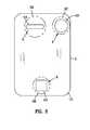
- FIG. 2is a diagrammatic illustration of a substrate with scribed closed form where the closed form is the desired part.
- FIG. 2Ais an enlarged portion of FIG. 1 illustrating the spacing between orifices/holes.
- FIG. 2Bis a diagrammatic cross-sectional view taken along the lines of 1 B- 1 B of FIG. 2A .
- FIG. 3is a diagrammatic illustration of a substrate with scribed closed form where the body is the desired part and the internal features will be cut out.
- FIG. 3Ais an enlargement of the slot illustrated in FIG. 3 .
- FIG. 3Bis an enlargement of a portion of FIG. 3A illustrating orifices and the crack line.
- FIG. 3Cis an enlargement of the circle cutout illustrated in FIG. 3 .
- FIG. 3Dis an enlargement of a portion of FIG. 3C illustrating orifices and the path of the crack line.
- FIG. 3Eis an enlargement of the square cutout of FIG. 3 .
- FIG. 3Fis an enlargement of a portion of FIG. 3E illustrating orifices and the path of the crack line.
- FIG. 4is another diagrammatic illustration of a closed form release (hard disk).
- FIG. 4Ais an enlargement of a portion of FIG. 4 illustrating orifices and the crack line.
- FIG. 5Ais an illustration of two sections cut from a transparent tube.
- FIG. 5Bis an enlargement of a portion of the tube illustrating orifices in the transparent tube and microcracks between the orifices.
- FIG. 6Ashows a plane of cleavage accomplished by successively drilling orifices through the transparent material
- FIG. 6Bshows an angled cut through a gemstone.
- FIGS. 7A-7Eshow the angled cut outs which make angled edges.
- FIGS. 8A-8Dillustrate different glass parts with cut outs.
- FIGS. 9A and 9Bare perspective and side views, respectively, of a via hole drilling in substrate.
- FIG. 10illustrates an embodiment for producing filaments that is suitable for wafer size substrate machining
- FIGS. 11A and 11Bare top and front views, respectively, of the layout of an example laser system suitable for part scribing
- FIG. 12is a side schematic view of a transparent substrate illustrating an incoming laser beam entering an aberrated focus lens, a metal layer engaging the bottom surface of the transparent substrate, photoresist engaging the metal layer, the principal focal waist of the laser beam residing on the surface of the photoresist, and secondary focal waists within the transparent substrate;
- FIG. 13is a side schematic view illustrating a transparent substrate with holes therethrough, the metal layer engaging the transparent substrate, photoresist engaging the metal layer, being wet etched—the transparent substrate, metal layer and photoresist are submersed in a chemical etchant;
- FIG. 13Ais a top view of the transparent substrate illustrated in FIG. 13 illustrating a plurality of holes through the substrate with a crack line formed between the holes thereof;
- FIG. 14is a side schematic view illustrating a transparent substrate with holes therethrough being dry etched, the transparent substrate has a metal layer in engagement with a surface of the transparent substrate and a layer of photoresist is in engagement with the metal layer.
- FIG. 1illustrates optical configurations for the formation of filaments in which long homogeneous filaments 220 are formed by focusing the beam energy such that it is “dumped” into a focus above and/or below the transparent target material (forming an optical reservoir 220 ) in order to modulate the amount of energy passed into the desired filament zone.
- Incoming laser beam 160passes through a distributed focus assembly 150 which creates foci above or below 210 the target substrate 215 .
- the filamentWhile optical break down which is the consequence of a tight focus inside the material (plasma void forms and laser focuses) the filament is the result of very mild focus using a NA of less than 0.4 where the focusing element only helps formation of the filament. While geometrical focus might have a 100 to 200 ⁇ m point spread function on the surface of target, the pulses self focus themselves to the 1 ⁇ m diameter range which in linear optics is possible by using a NA of 1 or higher (100 ⁇ objective oil immersed). While the terms “filament” or “plasma channel” are usually used as the standard terms for defining this process, some in the art describe this process as an “elongated focus” to describe the same effect. Elongated focus is the result of using ultrafast pulses. It is impossible to elongate, for example, long laser pulses and observe the same effect.
- 30 MHzis our standard burst frequency and single or multiple pulses can be picked at 100 kHz frequency to form the burst envelope.
- the single or multiple pulsescan be further amplified to reach 50 W average power at less than 15 ps.
- the burst envelopehas is 1-6 pulses therein and exceeds the critical power necessary to make filaments in the glass substrate.
- FIG. 2is a diagrammatic illustration of a substrate with scribed closed form where the closed form is the desired part.
- the closed form(desired part) is the part in the middle of FIG. 2 denoted by reference numeral 2 .
- product 2is the closed form that is the desired part formed via filamentation scribing on the main substrate 1 .
- solid line 21 Srepresents the scribed line which is cut into the surface 1 S of the substrate 1 .
- An example closed formcan be, but is not limited, to a smartphone cover glass or auto windshield, mirrors, architectural windows, etc.
- FIG. 2Ais an enlarged portion of FIG. 2 illustrating the spacing between holes (orifices) 21 B.
- Orifices 21 Bare approximately 1 ⁇ m diameter.
- Microcracks 21 Care illustrated between the orifices 21 B in FIG. 2A .
- Microcracks 21 Care created by a shock wave due to photoacoustic compression.
- the spacing between the holes (orifices)is 2-10 ⁇ m center to center as illustrated by reference numeral 25 depending on the type of form (sample type), substrate thickness and orifice depth.
- FIG. 2Bis a diagrammatic cross-sectional view taken along the lines of 1 B- 1 B of FIG. 2A .
- Orifice 21 Bextends completely through the substrate. All of the orifices drilled in the transparent substrate are substantially cylindrically shaped with no taper. Desired closed form can be released via different technique such as weakening the cut region by resting the sample in water for OH exchange, heating, cooling, or applying air pressure.
- One main aspect disclosed hereinis to use dry or wet chemical etching to remove the desired part from the body.
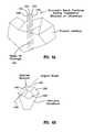
- FIG. 3is a diagrammatic illustration of a substrate 1 S with scribed closed forms, 33 , 43 , and 53 where the body 1 S is the desired part and the internal feature(s) are cut out (removed from the substrate).
- the closed formssuch as any one or a combination of slot 3 , circle 4 and cutout 5 made on the part 2
- any one or a combination of slot 3 , circle 4 and cutout 5can be dissolved and destroyed, to release any one or a combination of slot 3 , circle 4 and cutout 5 from the main body.
- the crack line of slot 3 , circle 4 or cutout 5are etched via Hydrofluoric acid bath for some time. This etching leads to much faster dissolution of the laser irradiated area causing full separation along the filament scribed line and the inner closed form drops by itself under its own weight.
- Circlescan be released with radii from 1 to 50 mm by creating a zone of photoacoustic compressed material in the substrate, then dropping in etching solution.
- FIG. 3Ais an enlargement of the slot 3 illustrated in FIG. 3 .
- FIG. 3Bis an enlargement of a portion of FIG. 3A illustrating orifices 33 and microcracks 33 C.
- FIG. 3Cis an enlargement of the circle cutout 4 illustrated in FIG. 3 .
- FIG. 3Dis an enlargement of a portion of FIG. 3C illustrating orifices 43 microcracks 43 C.
- FIG. 3Eis an enlargement of the square cutout 5 of FIG. 3 .
- FIG. 3Fis an enlargement of a portion of FIG. 3E illustrating orifices 53 and microcracks 53 C.
- the chemical bathis used to remove the cutouts.
- FIG. 4is another diagrammatic illustration of a closed form release. After the substrate is scribed, the platter is released from the main body (main portion) of the substrate 60 and also the central disk 80 is also released from the platter.
- FIG. 4Ais an enlargement of a portion of FIG. 4 illustrating orifices 81 E and microcracks 89 C.
- Orifices 81 Eextend through substrate 60 . All of the orifices 81 E drilled in the transparent substrate are substantially cylindrically shaped with no taper.
- Reference numeral 81 I in FIG. 4represents an inner scribed line in the shape of a circle and reference numeral 81 E represents an outer scribed line in the shape of a circle.
- scribedit is meant that the substrate includes orifices.
- Scribed circles 81 I, 81 Eare made in a matter of a second in the glass substrate 60 by the method of ultrafast burst filamentation to form perforations in the shapes of the circles. After etching the central circle 85 drops by itself under its own weight or just an air pressure or mechanical finger touch, and the disk 80 also releases from the cullet frame.
- disk 80is cut with a precision of 1 ⁇ m and with a facet roughness less than 1 ⁇ m. Since ultrafast burst filament scribing cuts the parts without any microcracks or edge chipping, there is no need for grinding.
- FIG. 5Ais an illustration of a spirally cut borosilicate tube.
- borosilicate glass rings sections 75 , 77are cut from a transparent tube 70 .
- FIG. 12Bis an enlargement of a portion of the tube illustrating orifices 12 D in the transparent tube 70 and microcracks 12 C between the orifices. The cut can be performed in a spiral motion to make a glass spring structure or tube itself can be a rod to make thin disks.
- FIG. 6Aa series of tightly spaced orifices 156 , 151 , 152 , 153 , 154 drilled through a gemstone such as diamond can be arranged so as to form a plane of cleavage 155 . Due to filament formation very narrow curtain of modified zone form the plane of cleavage. Placing the gemstone in the appropriate etching solution, the etching acid moves in the orifices due to the capillary effect and creates a good separation of the material. Using this technique, much less of the valuable stone is lost during cutting process.
- FIG. 6Bpresents the final stone after a few cuts.
- FIGS. 7A-Eshow the angled cut-out approach for making internal features with angled edges requiring no post singulation processing to achieve the desired angular result.
- the beam tracks 137 , 142is accomplished via rotation around the theta axis 136 with a fixed incidence angle from the laser beam, equal to the slope desired on the final part edge 765 .
- This non-limiting embodimentenables angled cutting and translation of the rotary stage as an apparatus to support the creation of complex cutouts via filament arrays.
- FIG. 7Eillustrates an example implementation of the formation of a chamfered part 140 via processing with multiple filament forming beams 142 at different angles.
- the beam and filament pathscan be controlled to form chamfered or bevel edges of various degrees.
- the edgemay be straight. By straight it is meant that it is perpendicular (normal) to the surface of the substrate.
- the beamcan be split and directed through optics to achieve multiple beam paths arriving at the target exhibiting angles of incidence other than normal, along with a normally incident beam, such that a three-face edge or chamfer is created.
- chamferscan be created with two or more faces, depending, for example, on the degree of splitting tolerated by the process.
- FIG. 7ESome example configurations are illustrated in FIG. 7E . After filament formation the samples are put in an etching bath for separation.
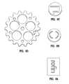
- FIGS. 8A-Dpresent very fine cut outs of variety of shapes in the substrate. Instead of marking the alphabet and numbers, business cards or advertisement logos can be made on the substrate instead of just marking. Very fine structures such as curved or angled channels, reservoirs, gears and such can be made in glass. This opens up huge applications in regard to glass and similar materials in MEMs production where making fine parts is costly and time consuming. The parts even can have metal coatings, and they can still be etched in the chemical bath or dry etch. Channels 50 ⁇ m wide are achieved in 200 ⁇ m thick glass and the etched cleave line always follows the scribed line.
- FIGS. 9A and Bare a top and isometric view of via hole drilling. Holes can be used for mass filtration, via holes in glass are also used inside microelectronics chips such as CPUs as insulators between the levels and interconnect through holes. Holes in sandwich glasses for material injection or for example on
- the mass separation device 68is simply a generally planar glass substrate 70 with an array of identically sized orifices 69 A (holes) drilled therethrough as illustrated in FIG. 10 .
- the material to be separated(whether gas, fluid or solid particles) is brought in contact with the planar face of the substrate 70 as a stream, such that the material passes over the orifice array 69 with a force sufficient to pass particles through the orifices in the substrate and beyond the bottom face of the device 68 .
- a force that is perpendicular to the plane of the deviceworks the fastest although any angle of the stream will work to a degree.
- the size of the orifices drilled in the substratewill be dictated by the geometric specifics of the item being separated.
- via holes in glassare in huge demand for interconnects in semiconductor devices. Due to very high frequencies used in CPUs, using long wires to connect the circuits results in radiation. To avoid stacks of chips, very thin layers of glass are used as insulation layers between the chips. From level to level connections are made using through via holes. More than 100 thousand holes are sometimes needed in one sample. Holes made by laser ablation using ultrafast burst filamentation the holes (mini circles) can be scribed and later removed via chemical etching. This speeds up the manufacturing and reduces the cost per part.
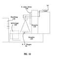
- FIG. 10illustrates the layout of an example laser system suitable for part singulation.
- Laser 72is capable of delivering burst pulses, for example, with energies in the range of approximately 1 ⁇ J-50 mJ, at a repetition rate of up to approximately 2.5 MHz.
- Granite riser 118is designed to be a reactive mass for dampening mechanical vibrations, as is commonly used in industry. This could be a bridge on which the optics above the stage can translate along one axis, X or Y relative to the stage, and in coordination with it.
- Granite base 120provides a reactive mass that may support any or all components of system.
- handling apparatus 122is vibrationally decoupled from the system for stability reasons.
- Z axis motor drive 124is provided for translating the optics (conditioning and focusing and scan optics if needed) in the Z axis relative to the servo controlled X-Y stage 84 .
- This motioncan be coordinated with the XY stage 84 and X or Y motion in the overhead granite bridge, and the XY motion of the stage on the granite base 120 , which holds the sample material to be processed.
- Stage 84includes, for example, XY and Theta stages with a tilt axis, gamma (“yaw”).
- the motion of stages 84is coordinated by a control computing system, for example, to create a part shape desired from a larger mother sheet.
- Metrology device 108provides post processing or preprocessing (or both) measurements, for example, for mapping, sizing, and/or checking edges quality post cut.
- FIG. 11Ais a schematic top view of an example laser system for cutting glass hard disk drive platters 180 using laser machining.
- X-Y motion of the laser head 177is illustrated in FIG. 10A wherein the laser head 177 is illustrated schematically above glass substrate 170 .
- Glass substrate 170is supported by beams 171 , 172 above a granite (or other dimensionally stable) support 120 .
- Rails 175 , 176support the movable arm 178 which is movable in the X direction along the rails 175 , 176 as illustrated in FIG. 10A .
- Movable arm 178is driven by a motor and a controller which precisely positions the movable arm 178 in the X direction.
- FIG. 11Bis a schematic side view of the example laser system for cutting glass hard disk drive platters illustrated in FIG. 11A .
- Movable arm 178includes rail means and the laser head 177 includes a motor 177 M or other means for positioning the laser head 177 in the Y direction. Further the laser head in movable in the Z direction for adjusting the beam waists as desired. Vertical rail 177 V enables movement of the laser head 177 in the vertical direction (the Z direction). Still further, it is understood that a selected distributive-focus lens may be adapted for use with the laser head 177 . Glass hard disk drive platters 180 are illustrated in FIG. 25A and in FIG. 4 .
- the hard disk just describedwas just an example, it can be almost any part made of brittle material in flat or curved form.
- FIG. 12is a side schematic view of a transparent substrate 150 T illustrating an incoming laser beam 150 I entering an aberrated focus lens 150 , a metal layer 150 M engaging the bottom surface of the transparent substrate, photoresist 150 R engaging the metal layer 150 M, the principal focal waist 150 P of the laser beam residing on the surface of the photoresist 150 R, and secondary focal waists 150 S within the transparent substrate 150 T.
- FIG. 13is a side schematic view illustrating a transparent substrate 150 T with holes 150 H therethrough, the metal layer 150 M engaging the transparent substrate 150 T, photoresist 150 R engaging the metal layer 150 M, being wet etched—the transparent substrate 150 T, metal layer 150 M and photoresist 150 R are submersed in a chemical etchant 301 .
- the desired portion of the transparent substrate 180is separated from the remainder portion of the transparent substrate 150 T by gravity after the transparent substrate resides in the etchant for a sufficient time.
- Supports 302 A, 302 B and 301 Creside beneath the remainder portion of the transparent substrate.
- the remainder portionis the portion that is left behind after the desired portion has been removed therefrom.
- the arrangement illustrated in FIG. 13is within a container 303 full of etchant 301 .
- the etchantresides within the holes 150 H of the substrate and weakens exposed surfaces of the holes 150 H of the transparent substrate 150 T.
- the wet etchantmay be any of those previously identified herein suitable for use with transparent substrates identified herein.
- FIG. 13Ais a top view of the transparent substrate 150 T illustrated in FIG. 13 illustrating a plurality of holes through the substrate with crack lines 151 C, 152 C formed between the holes 150 H thereof.
- the holes 150 Hare very small diameter holes as explained herein with other drawing figures. Holes 150 H are closely spaced together. Holes 150 H are made by laser filamentation. Preferably, the spacing between the holes (orifices) is 2-10 ⁇ m center to center. Holes 150 H are less than or equal to approximately 1 ⁇ m in diameter. Crack lines 151 C, 152 C are formed between adjacent holes 150 H resulting in a smooth surface when the desired part 180 is separated from the substrate 150 T.
- the desired partin this example a disk 180 , may be separated when removed from the bath 301 under its own weight or the slight urging of a mechanical device, a mechanical finger (not shown), or air pressure.
- the capillary effectassists in drawing the wet etchant 301 into the holes 150 H which extend through the substrate.
- the capillary effectis present due to the extremely small diameter holes that are made by the filamentation process described herein. Still referring to FIG. 13 the holes 150 H are filled with etchant 301 .
- the etchant symbol(the fluid symbol) is not used in the holes 150 H because it would be difficult to see in drawing FIG. 13 .
- Etchant 301 within the holes 150 Hweakens the transparent material along the crack line of the transparent material facilitating separation of the parts with smooth edges.
- FIG. 14is a side schematic view illustrating a transparent substrate 150 T with holes 150 H therethrough being dry etched, the transparent substrate 150 T has a metal layer 150 M in engagement with a surface of the transparent substrate and a layer of photoresist 150 R in engagement with the metal layer 150 M. Electrodes 190 A, 190 C are excited by an RF voltage source which acts on the gas/plasma 150 G between the electrodes which excites the dry etchant.
- the etchantresides within the holes 150 H of the substrate and weakens exposed surfaces of the holes 150 H of the transparent substrate 150 T.
- the dry etchantmay be any of those etchants previously identified herein suitable for use on the transparent substrates identified herein. None herein limits the type of dry etching that is used.
- An exemplary method of laser processing a transparent material 150 Tincludes the following the steps.
- the transparent materialhas a metal layer 150 M formed in engagement with the transparent material and the metal layer 150 M has a photoresist layer 150 R formed in engagement with the metal layer 150 M.
- a laser beam 150 IFIG. 12
- the laser beamincludes a burst of laser pulses, the burst of laser pulses may be a single pulse or multiple pulses.
- the laser pulsesare focused such that sufficient energy density is maintained within the transparent material to form a continuous laser filament therein without causing optical breakdown.
- the processrequires simultaneously forming the continuous laser filament ( 220 , FIG. 1 ) within the transparent material and simultaneously forming a low-power laser beam to ablate the photoresist layer 150 R and the metal layer 150 M, the power of the filament-forming laser beam is reduced below the threshold for the simultaneous of the filament within and through the transparent material while maintaining sufficient power to ablate and irradiate the photoresist layer 150 R and the metal layer 150 M with the low-power laser beam at one or more locations such that the metal layer 150 M is locally ablated by the laser beam thereby removing the metal layer 150 M in proximity to a hole 150 H through the transparent material 150 T formed by the continuous laser filament.
- the continuous laser filamentis formed within and through the substrate at the same time the photoresist layer and the metal layer are ablated and removed.
- the holesmay be etched using a wet or dry process.
- the processrequires selectively etching the hole 150 H through the transparent material while the remaining photoresist 150 R avoids damage to the metal layer.
- the photoresisteffectively eliminates collateral damage to the metal layer by preventing exposure of the wet or dry etchant to the metal layer.
- the photoresist layer and the metal layerare removed in proximity to holes 150 H as shown in FIGS. 13 and 14 . It should be noted that various masks can be used in both the wet etching process and the dry etching process.
- the photoresist layer and the metal layerare removed simultaneously with the formation of a filament(s). See FIG. 14 .
- the inventionis also suitable for printing metal on a transparent material.
- the transparent materialreceives a layer of metal thereon and then a layer of photoresist is applied to the metal.
- a maskis then applied to the metal layer.
- the maskprevents light from reaching the photoresist underneath the mask.
- the maskforms, for instance, the letter A.
- Suitable lightis applied to the photoresist which is exposed and not covered by the mask. Since the invention teaches simultaneous ablation of the photoresist, ablation of the metal, and formation of holes through the transparent material by photoacoustic compression, techniques for etching the metal and the transparent material can be used to produce a high quality letter A.
Landscapes
- Physics & Mathematics (AREA)
- Optics & Photonics (AREA)
- Engineering & Computer Science (AREA)
- Mechanical Engineering (AREA)
- Plasma & Fusion (AREA)
- Chemical & Material Sciences (AREA)
- Inorganic Chemistry (AREA)
- Laser Beam Processing (AREA)
- Re-Forming, After-Treatment, Cutting And Transporting Of Glass Products (AREA)
- Surface Treatment Of Glass (AREA)
- General Physics & Mathematics (AREA)
Abstract
Description
- This patent application claims the benefit and priority of U.S. provisional patent application Ser. No. 62/103,031 filed Jan. 13, 2015. U.S. provisional patent application Ser. No. 62/103,031 filed Jan. 13, 2015 is incorporated herein by reference hereto in its entirety.
- U.S. patent application Ser. No. 13/640,140, filed Jan. 31, 2013, U.S. patent application Ser. No. 14/336,912, filed Jul. 21, 2014, and U.S. patent application Ser. No. 14/336,819, filed Jul. 21, 2014 are hereby incorporated herein by reference hereto as if fully written herein.
- The present disclosure is related to systems and methods for the laser processing of materials. More particularly, the present disclosure is related to systems and methods for the singulation and/or cleaving of wafers, substrates, and plates containing passive or active electronic or electrical devices created upon said materials.
- In current manufacturing, the singulation, dicing, scribing, cleaving, cutting, and facet treatment of wafers or glass panels is a critical processing step that typically relies on diamond or conventional, ablative or breakdown (stealth) laser scribing and cutting, with speeds of up to 30 cm/sec for LEDs, LED devices (such as lighting assemblies) and illuminated devices (such as LED displays) as some examples.
- In the diamond cutting process, after diamond cutting is performed, a mechanical roller applies stress to propagate cracks that cleave the sample. This process creates poor quality edges, microcracks, wide kerf width, and substantial debris that are major disadvantages in the lifetime, efficiency, quality, and reliability of the product, while also incurring additional cleaning and polishing steps. The cost of de-ionized water to run the diamond scribers are more than the cost of ownership of the scriber and the technique is not environmentally friendly since water becomes contaminated and needs refining, which further adds to the production cost.
- Laser ablative machining has been developed for singulation, dicing, scribing, cleaving, cutting, and facet treatment, to overcome some of the limitations associated with diamond cutting. Unfortunately, known laser processing methods have disadvantages, particularly in transparent materials, such as slow processing speed, generation of cracks, contamination by ablation debris, and moderated sized kerf width. Furthermore, thermal transport during the laser interaction can lead to large regions of collateral thermal damage (i.e. heat affected zone).
- Laser ablation processes can be improved by selecting lasers with wavelengths that are strongly absorbed by the medium (for example, deep UV excimer lasers or far-infrared CO2laser). However, the aforementioned disadvantages cannot be eliminated due to the aggressive interactions inherent in this physical ablation process. This is amply demonstrated by the failings of UV processing in certain LED applications where damage has driven the industry to focus on traditional scribe and break followed by etching to remove the damaged zones left over from the ablative scribe or the diamond scribe tool, depending upon the particular work-around technology employed.
- Alternatively, laser ablation can also be improved at the surface of transparent media by reducing the duration of the laser pulse. This is especially advantageous for lasers that are transparent inside the processing medium. When focused onto or inside transparent materials, the high laser intensity induces nonlinear absorption effects to provide a dynamic opacity that can be controlled to accurately deposit appropriate laser energy into a small volume of the material as defined by the focal volume. The short duration of the pulse offers several further advantages over longer duration laser pulses such as eliminating plasma creation and therefor plasma reflections thereby reducing collateral damage through the small component of thermal diffusion and other heat transport effects during the much shorter time scale of such laser pulses.
- Femtosecond and picosecond laser ablation, therefore, offer significant benefits in machining of both opaque and transparent materials. However, in general, the machining of transparent materials with pulses even as short as tens to hundreds of femtoseconds is also associated with the formation of rough surfaces, slow throughput and micro-cracks in the vicinity of laser-formed kerf, hole or trench that is especially problematic for brittle materials like alumina (Al2O3), glasses, doped dielectrics and optical crystals. Further, ablation debris will contaminate the nearby sample and surrounding devices and surfaces. Recently, multi-pass femtosecond cutting has been discussed in Japan, utilizing a fiber laser approach. This approach suffers from the need to make multiple passes and therefore results in low processing throughput.
- Although laser processing has been successful in overcoming many of the limitations associated with diamond cutting, as mentioned above, new material compositions have rendered the wafers and panels incapable of being laser scribed. Furthermore, the size of the devices and dice on the wafers are getting smaller and closer to each other that limit the utility of both diamond and conventional laser-based scribing. For example, 30 μm is a feasible scribing width, while 15 μm is challenging for these conventional methods. Moreover, as diamond scribing uses mechanical force to scribe the substrate, thin samples are very difficult to scribe. Due to the use of increasingly exotic and complex material stacks in the fabrication of wafer-based devices, the laser scribing techniques previously applied will simply no longer work due to the opacity of the stack.
- Systems and methods are described for forming continuous laser filaments in transparent materials. The transparent material may be selected from the group consisting of glass, borosilicate glass, amber glass, chemically or heat strengthened glass, sapphire, LiNbO3, Silicon, Ti: Sapphire, LiTaO3, transparent ceramics (including the optical ceramic ALON), crystalline rods, GaN, SiC and ZnSe.
- A burst of ultrafast laser pulses is focused such that a beam waist is formed external to the material being processed, such that a primary focus does not form within the material, while a sufficient energy density is formed within an extended region within the material to support the formation of a continuous filament, without causing optical breakdown within the material. Filaments formed according to this method may exhibit lengths exceeding up to 10 mm with a 1:1 correspondence in the length of the modified zone (in that the filament is the agent of modification, so the modified zone tracks 1:1 with the extent of the filament) and a taper-free profile when viewed with the long axis in cross-section. In some embodiments, an uncorrected or aberrated optical focusing element is employed to produce an external beam waist while producing distributed focusing (elongated focus) of the incident beam within the material. Various systems are described that facilitate the formation of filament arrays within transparent substrates for cleaving/singulation and/or marking. Optical monitoring of the filaments may be employed to provide feedback to facilitate active control of the process.
- Accordingly, in a first aspect, there is provided a method of laser processing a transparent material, the method comprising:
- a laser source configured to provide a laser beam comprising bursts of laser pulses;
- one or more focusing elements configured to externally focus the laser beam relative to the transparent material to form a beam waist at a location external to the transparent material while avoiding the formation of an external plasma channel;
- the laser beam and one or more focusing elements are configured to produce sufficient energy density within the transparent material to form a continuous laser filament therein without causing optical breakdown;
- means for varying a relative position between the laser beam and the transparent material;
- a control and processing unit operatively coupled to the means for varying the relative position between the laser beam and the transparent material;
- the control and processing unit is configured to control the relative position between the laser beam and the transparent material for the formation of an array of continuous laser filaments within the transparent material;
- the array of continuous laser filaments extending continuously from a first surface of the transparent material to a second surface of the transparent material; and,
- selectively wet or dry etching the array of continuous laser filaments for releasing the closed form
- In another aspect, there is provided a method of processing a transparent material, comprising the steps of:
- the transparent material has a metal layer formed in engagement with the transparent material and the metal layer has a photoresist layer formed in engagement with the metal layer,
- providing a laser beam, the laser beam includes a burst of laser pulses, the burst of laser pulses may be a single pulse or multiple pulses;
- externally focusing the laser beam relative to the transparent material to form a beam waist at a location that is external to the transparent material while avoiding the formation of an external plasma channel;
- the laser pulses are focused such that sufficient energy density is maintained within the transparent material to form a continuous laser filament therein without causing optical breakdown;
- simultaneously forming the continuous laser filament within the transparent material and simultaneously forming a low-power laser beam to ablate the photoresist layer and the metal layer, the power of the filament-forming laser beam is reduced below the threshold for the simultaneous of the filament within and through the transparent material while maintaining sufficient power to ablate and irradiate the photoresist layer and the metal layer with the low-power laser beam at one or more locations such that the metal layer is locally ablated by the laser beam thereby removing the metal layer in proximity to a hole through the transparent material formed by the continuous laser filament; and,
- selectively etching the hole through the substrate of the transparent material while the photoresist avoids damage to damage to the metal layer.
- In another aspect, there is provided a method of processing a transparent material, comprising the steps of:
- the transparent material has a metal layer formed in engagement with the transparent material and the metal layer has a photoresist layer formed in engagement with the metal layer;
- providing a laser beam, the laser beam includes a burst of laser pulses, the burst of laser pulses may be a single pulse or multiple pulses;
- externally focusing the laser beam relative to the transparent material to form a beam waist at a location that is external to the transparent material while avoiding the formation of an external plasma channel;
- the laser pulses are focused such that sufficient energy density is maintained within the transparent material to form a continuous laser filament therein without causing optical breakdown;
- simultaneously forming the continuous laser filament within the transparent material and simultaneously forming a low-power laser beam to ablate the photoresist layer and the metal layer, the power of the filament-forming laser beam is reduced below the threshold for the simultaneous of the filament within and through the transparent material while maintaining sufficient power to ablate and irradiate the photoresist layer and the metal layer with the low-power laser beam at one or more locations such that the metal layer is locally ablated by the laser beam thereby removing the metal layer in proximity to a hole through the transparent material formed by the continuous laser filament;
- creating a plurality of holes through the transparent substrate and removing a portion of the metal layer and a portion of the photoresist layer in proximity to each one of the holes of the plurality of holes through the substrate; and,
- selectively etching the hole through the substrate of the transparent material while the photoresist avoids damage to damage to the metal layer.
- In another aspect, there is provided a method of processing a transparent material, comprising the steps of:
- the transparent material includes a metal layer in engagement with the transparent material, and, a photoresist layer resides in engagement with the metal layer;
- providing a laser beam, the laser beam having a plurality of bursts and each of the bursts include a plurality of pulses;
- generating an initial waist of the laser beam outside the transparent material using an uncorrected or aberrated optical focusing element;
- generating a weakly focused laser beam distributed within the transparent material;
- producing a spatially extended and spatially homogenous filament in the transparent material;
- forming an array of filaments within the transparent substrate;
- removing a portion of the metal layer and a portion of the photoresist proximate each of the continuous laser filaments; and,
- selectively dry or wet etching the array of continuous laser filaments.
- In another aspect there is provided a transparent material having a continuous laser filament formed there
- In another aspect there is provided a transparent material having a continuous laser filament formed therein, the continuous laser filament having a length exceeding approximately 1 mm.
- In another aspect, there is provided a transparent substrate exhibiting a post-cleave or post-singulation break strength that exceeds approximately 50 MPa.
- Very fine closed form structures can be scribed via filamentation in the transparent substrate very quickly, the modified zone can be etched via dry or wet chemical etching to release the closed form.
- The transparent material is selected from the group consisting of glass, borosilicate glass, amber glass, chemically or heat strengthened glass, sapphire, LiNbO3, Silicon, Ti: Sapphire, LiTaO3, transparent ceramics (like ALON) crystalline rods, GaN, SiC and ZnSe.
- The dry etchants include, but are not limited to, the following: Carbon Tetrafluoride CF4, Sulfur Hexafluoride SF6, Nitrogen Trifluoride NF3, Chlorine Cl2, and Dichlordifluoro methane CCl2F2. The wet etchants include, but are not limited to, the following: Nitric acid (HNO3) and Hydrofluoric acid (HF), Potassium hydroxide (KOH), Ethylenediamine pyrocatechol (EDP), and Tetramethylammonium hydroxide (TMAH).
- A further understanding of the functional and advantageous aspects of the disclosure can be realized by reference to the following detailed description and drawings.
FIG. 1 illustrates optical configurations for the formation of filaments in which long homogeneous filaments are formed by focusing the beam energy such that it is “dumped” into a focus above and/or below the target transparent material (forming an “optical reservoir”) in order to modulate the amount of energy passed into the desired filament zone.FIG. 2 is a diagrammatic illustration of a substrate with scribed closed form where the closed form is the desired part.FIG. 2A is an enlarged portion ofFIG. 1 illustrating the spacing between orifices/holes.FIG. 2B is a diagrammatic cross-sectional view taken along the lines of1B-1B ofFIG. 2A .FIG. 3 is a diagrammatic illustration of a substrate with scribed closed form where the body is the desired part and the internal features will be cut out.FIG. 3A is an enlargement of the slot illustrated inFIG. 3 .FIG. 3B is an enlargement of a portion ofFIG. 3A illustrating orifices and the crack line.FIG. 3C is an enlargement of the circle cutout illustrated inFIG. 3 .FIG. 3D is an enlargement of a portion ofFIG. 3C illustrating orifices and the path of the crack line.FIG. 3E is an enlargement of the square cutout ofFIG. 3 .FIG. 3F is an enlargement of a portion ofFIG. 3E illustrating orifices and the path of the crack line.FIG. 4 is another diagrammatic illustration of a closed form release (hard disk).FIG. 4A is an enlargement of a portion ofFIG. 4 illustrating orifices and the crack line.FIG. 5A is an illustration of two sections cut from a transparent tube.FIG. 5B is an enlargement of a portion of the tube illustrating orifices in the transparent tube and microcracks between the orifices.FIG. 6A shows a plane of cleavage accomplished by successively drilling orifices through the transparent material; andFIG. 6B shows an angled cut through a gemstone.FIGS. 7A-7E show the angled cut outs which make angled edges.FIGS. 8A-8D illustrate different glass parts with cut outs.FIGS. 9A and 9B are perspective and side views, respectively, of a via hole drilling in substrate.FIG. 10 illustrates an embodiment for producing filaments that is suitable for wafer size substrate machiningFIGS. 11A and 11B are top and front views, respectively, of the layout of an example laser system suitable for part scribing;FIG. 12 is a side schematic view of a transparent substrate illustrating an incoming laser beam entering an aberrated focus lens, a metal layer engaging the bottom surface of the transparent substrate, photoresist engaging the metal layer, the principal focal waist of the laser beam residing on the surface of the photoresist, and secondary focal waists within the transparent substrate;FIG. 13 is a side schematic view illustrating a transparent substrate with holes therethrough, the metal layer engaging the transparent substrate, photoresist engaging the metal layer, being wet etched—the transparent substrate, metal layer and photoresist are submersed in a chemical etchant;FIG. 13A is a top view of the transparent substrate illustrated inFIG. 13 illustrating a plurality of holes through the substrate with a crack line formed between the holes thereof; and,FIG. 14 is a side schematic view illustrating a transparent substrate with holes therethrough being dry etched, the transparent substrate has a metal layer in engagement with a surface of the transparent substrate and a layer of photoresist is in engagement with the metal layer.- Embodiments of the disclosure will now be described by way of example only.
FIG. 1 illustrates optical configurations for the formation of filaments in which longhomogeneous filaments 220 are formed by focusing the beam energy such that it is “dumped” into a focus above and/or below the transparent target material (forming an optical reservoir220) in order to modulate the amount of energy passed into the desired filament zone.Incoming laser beam 160 passes through a distributedfocus assembly 150 which creates foci above or below210 thetarget substrate 215.- The propagation of ultrafast laser pulses in transparent optical media is complicated by the strong reshaping of the spatial and temporal profile of the laser pulse through a combined action of linear and nonlinear effects such as group-velocity dispersion (GVD), linear diffraction, self-phase modulation (SPM), self-focusing, multiphoton/tunnel ionization (MPI/TI) of electrons from the valence band to the conduction band, plasma defocusing, and self-steepening. See SL Chin et al. Canadian Journal of Physics, 83, 863-905 (2005). These effects play out to varying degrees that depend on the laser parameters, material nonlinear properties, and the focusing condition into the material. Due to the dependence of nonlinear refractive index to intensity, during the propagation of intense laser pulses, the central part of the pulse moves slower than the surrounding parts of the pulse due to variable refractive index that causes the pulse to self-focus. In the self focusing region due to MPI/TI plasma generated, plasma acts as negative lens and defocuses the pulse but due to high intensity self-focusing occurs again. The balancing act between focusing and defocusing creates a long plasma channel that is known as filament. Using a low per pulse energy filament leaves traces of refractive index modification in the material. The filament is surrounded by background energy that pumps energy to form the filament. This background energy is known as a filament reservoir in the art. Blocking or disturbing a portion of reservoir will have the effect of losing the filament. For this reason the space separation between the filaments is crucial for filament forming. Otherwise damage and cracks form in the substrate instead of scribing. During filament formation a photoacoustic effect takes place which is inherent of plasma generation. This opens up less than 1 μm diameter confined holes into the substrate and depending on the laser input power can reach up to 10 mm long without changing the diameter. For this reason it is possible to stack many sheets of flat substrates and scribe all of them in single motion. Filaments can form using a single pulse ultrafast laser inside the material as far as higher than critical peak power for that specified material is used. While using multiple pulses as train of pulses or burst helps for much better filament formation due to heat accumulation and consecutive photoacoustic shock wave generation. While optical break down which is the consequence of a tight focus inside the material (plasma void forms and laser focuses) the filament is the result of very mild focus using a NA of less than 0.4 where the focusing element only helps formation of the filament. While geometrical focus might have a 100 to 200 μm point spread function on the surface of target, the pulses self focus themselves to the 1 μm diameter range which in linear optics is possible by using a NA of 1 or higher (100× objective oil immersed). While the terms “filament” or “plasma channel” are usually used as the standard terms for defining this process, some in the art describe this process as an “elongated focus” to describe the same effect. Elongated focus is the result of using ultrafast pulses. It is impossible to elongate, for example, long laser pulses and observe the same effect.
- Others in the art describe this process as “burst ultrafast filament formation” and claim that the first pulse makes a waveguide and that consecutive pulses follow the waveguide.
- Meanwhile the heat accumulation effect would disappear if a burst frequency of 1 MHz or lower is used. Heat accumulation works very well to produce well pronounced filaments when 30 to 60 MHz burst frequency. At this condition a narrow crack less than 100 nm wide forms from filament to filament. This creates a curtain (crack wall) all the way from top to bottom of the sample along the scribe line. Applying leak detector dye proved that dye can pass through the scribe line and end up on another surface. The capillary effect enables dye to travel all the way inside the crack curtain and filament channels.
- While we disclose use of a 30 MHz seeder in the Rofin StarPico model, 30 MHz is our standard burst frequency and single or multiple pulses can be picked at 100 kHz frequency to form the burst envelope. The single or multiple pulses can be further amplified to reach 50 W average power at less than 15 ps. The burst envelope has is 1-6 pulses therein and exceeds the critical power necessary to make filaments in the glass substrate.
FIG. 2 is a diagrammatic illustration of a substrate with scribed closed form where the closed form is the desired part. The closed form (desired part) is the part in the middle ofFIG. 2 denoted byreference numeral 2.- There are clearly two strategies when the main body or closed form is the desired part. As shown in
FIG. 2 ,product 2 is the closed form that is the desired part formed via filamentation scribing on themain substrate 1. Referring toFIG. 2 ,solid line 21S represents the scribed line which is cut into thesurface 1S of thesubstrate 1. An example closed form can be, but is not limited, to a smartphone cover glass or auto windshield, mirrors, architectural windows, etc. FIG. 2A is an enlarged portion ofFIG. 2 illustrating the spacing between holes (orifices)21B.Orifices 21B are approximately 1 μm diameter.Microcracks 21C are illustrated between theorifices 21B inFIG. 2A .Microcracks 21C are created by a shock wave due to photoacoustic compression. The spacing between the holes (orifices) is 2-10 μm center to center as illustrated byreference numeral 25 depending on the type of form (sample type), substrate thickness and orifice depth.FIG. 2B is a diagrammatic cross-sectional view taken along the lines of1B-1B ofFIG. 2A .Orifice 21B extends completely through the substrate. All of the orifices drilled in the transparent substrate are substantially cylindrically shaped with no taper. Desired closed form can be released via different technique such as weakening the cut region by resting the sample in water for OH exchange, heating, cooling, or applying air pressure. One main aspect disclosed herein is to use dry or wet chemical etching to remove the desired part from the body.FIG. 3 is a diagrammatic illustration of asubstrate 1S with scribed closed forms,33,43, and53 where thebody 1S is the desired part and the internal feature(s) are cut out (removed from the substrate). As shown inFIG. 3 , when the closed forms such as any one or a combination ofslot 3,circle 4 andcutout 5 made on thepart 2 is not the desired part, any one or a combination ofslot 3,circle 4 andcutout 5 can be dissolved and destroyed, to release any one or a combination ofslot 3,circle 4 andcutout 5 from the main body. The crack line ofslot 3,circle 4 orcutout 5 are etched via Hydrofluoric acid bath for some time. This etching leads to much faster dissolution of the laser irradiated area causing full separation along the filament scribed line and the inner closed form drops by itself under its own weight.- Circles (circular cut-outs), for example, can be released with radii from 1 to 50 mm by creating a zone of photoacoustic compressed material in the substrate, then dropping in etching solution.
FIG. 3A is an enlargement of theslot 3 illustrated inFIG. 3 .FIG. 3B is an enlargement of a portion ofFIG. 3A illustrating orifices 33 andmicrocracks 33C.FIG. 3C is an enlargement of thecircle cutout 4 illustrated inFIG. 3 .FIG. 3D is an enlargement of a portion ofFIG. 3C illustrating orifices 43microcracks 43C.FIG. 3E is an enlargement of thesquare cutout 5 ofFIG. 3 .FIG. 3F is an enlargement of a portion ofFIG. 3E illustrating orifices 53 andmicrocracks 53C. In all of the examples the chemical bath is used to remove the cutouts.- Scribing glass in two circles to form a disk used for hard disk drive is challenging for industry. In the related art, after diamond roller scribing, facet quality is very poor necessitating grinding that adds to product cost.
FIG. 4 is another diagrammatic illustration of a closed form release. After the substrate is scribed, the platter is released from the main body (main portion) of thesubstrate 60 and also thecentral disk 80 is also released from the platter. FIG. 4A is an enlargement of a portion ofFIG. 4 illustrating orifices 81E and microcracks89C.Orifices 81E extend throughsubstrate 60. All of theorifices 81E drilled in the transparent substrate are substantially cylindrically shaped with no taper.- Reference numeral81I in
FIG. 4 , represents an inner scribed line in the shape of a circle andreference numeral 81E represents an outer scribed line in the shape of a circle. By scribed it is meant that the substrate includes orifices. - Scribed circles81I,81E are made in a matter of a second in the
glass substrate 60 by the method of ultrafast burst filamentation to form perforations in the shapes of the circles. After etching the central circle85 drops by itself under its own weight or just an air pressure or mechanical finger touch, and thedisk 80 also releases from the cullet frame. - Still referring to
FIG. 4 ,disk 80 is cut with a precision of 1 μm and with a facet roughness less than 1 μm. Since ultrafast burst filament scribing cuts the parts without any microcracks or edge chipping, there is no need for grinding. FIG. 5A , is an illustration of a spirally cut borosilicate tube. One can see the applicability of being able to cleanly, cut curved surfaces from transparent materials. Here borosilicate glass ringssections transparent tube 70.FIG. 12B is an enlargement of a portion of thetube illustrating orifices 12D in thetransparent tube 70 andmicrocracks 12C between the orifices. The cut can be performed in a spiral motion to make a glass spring structure or tube itself can be a rod to make thin disks.- As shown in
FIG. 6A a series of tightly spacedorifices cleavage 155. Due to filament formation very narrow curtain of modified zone form the plane of cleavage. Placing the gemstone in the appropriate etching solution, the etching acid moves in the orifices due to the capillary effect and creates a good separation of the material. Using this technique, much less of the valuable stone is lost during cutting process.FIG. 6B presents the final stone after a few cuts. FIGS. 7A-E show the angled cut-out approach for making internal features with angled edges requiring no post singulation processing to achieve the desired angular result. InFIGS. 7A-E , the beam tracks137,142 is accomplished via rotation around thetheta axis 136 with a fixed incidence angle from the laser beam, equal to the slope desired on the final part edge765. This non-limiting embodiment enables angled cutting and translation of the rotary stage as an apparatus to support the creation of complex cutouts via filament arrays.FIG. 7E illustrates an example implementation of the formation of achamfered part 140 via processing with multiplefilament forming beams 142 at different angles. It is to be understood that the beam and filament paths can be controlled to form chamfered or bevel edges of various degrees. Further, it is understood that the edge may be straight. By straight it is meant that it is perpendicular (normal) to the surface of the substrate. In the case of concerted (parallel) formation, the beam can be split and directed through optics to achieve multiple beam paths arriving at the target exhibiting angles of incidence other than normal, along with a normally incident beam, such that a three-face edge or chamfer is created.- It is to be understood that chamfers can be created with two or more faces, depending, for example, on the degree of splitting tolerated by the process. Some example configurations are illustrated in
FIG. 7E . After filament formation the samples are put in an etching bath for separation. FIGS. 8A-D present very fine cut outs of variety of shapes in the substrate. Instead of marking the alphabet and numbers, business cards or advertisement logos can be made on the substrate instead of just marking. Very fine structures such as curved or angled channels, reservoirs, gears and such can be made in glass. This opens up huge applications in regard to glass and similar materials in MEMs production where making fine parts is costly and time consuming. The parts even can have metal coatings, and they can still be etched in the chemical bath or dry etch. Channels 50 μm wide are achieved in 200 μm thick glass and the etched cleave line always follows the scribed line.FIGS. 9A and B are a top and isometric view of via hole drilling. Holes can be used for mass filtration, via holes in glass are also used inside microelectronics chips such as CPUs as insulators between the levels and interconnect through holes. Holes in sandwich glasses for material injection or for example on- As shown in
FIGS. 9A and B themass separation device 68 is simply a generallyplanar glass substrate 70 with an array of identicallysized orifices 69A (holes) drilled therethrough as illustrated inFIG. 10 . In operation, the material to be separated (whether gas, fluid or solid particles) is brought in contact with the planar face of thesubstrate 70 as a stream, such that the material passes over theorifice array 69 with a force sufficient to pass particles through the orifices in the substrate and beyond the bottom face of thedevice 68. In theory, a force that is perpendicular to the plane of the device works the fastest although any angle of the stream will work to a degree. The size of the orifices drilled in the substrate will be dictated by the geometric specifics of the item being separated. - There is a huge demand to make holes of 50 to 1000 μm diameter in 50 μm up to 5 mm thick transparent material. It seems the current method is the best and most efficient way of making these via holes. As another example, via holes in glass are in huge demand for interconnects in semiconductor devices. Due to very high frequencies used in CPUs, using long wires to connect the circuits results in radiation. To avoid stacks of chips, very thin layers of glass are used as insulation layers between the chips. From level to level connections are made using through via holes. More than 100 thousand holes are sometimes needed in one sample. Holes made by laser ablation using ultrafast burst filamentation the holes (mini circles) can be scribed and later removed via chemical etching. This speeds up the manufacturing and reduces the cost per part.
FIG. 10 illustrates the layout of an example laser system suitable for part singulation.Laser 72 is capable of delivering burst pulses, for example, with energies in the range of approximately 1 μJ-50 mJ, at a repetition rate of up to approximately 2.5 MHz.Granite riser 118 is designed to be a reactive mass for dampening mechanical vibrations, as is commonly used in industry. This could be a bridge on which the optics above the stage can translate along one axis, X or Y relative to the stage, and in coordination with it.Granite base 120 provides a reactive mass that may support any or all components of system. In some embodiments,handling apparatus 122 is vibrationally decoupled from the system for stability reasons.- Z
axis motor drive 124 is provided for translating the optics (conditioning and focusing and scan optics if needed) in the Z axis relative to the servo controlledX-Y stage 84. This motion can be coordinated with theXY stage 84 and X or Y motion in the overhead granite bridge, and the XY motion of the stage on thegranite base 120, which holds the sample material to be processed. Stage 84 includes, for example, XY and Theta stages with a tilt axis, gamma (“yaw”). The motion ofstages 84 is coordinated by a control computing system, for example, to create a part shape desired from a larger mother sheet.Metrology device 108 provides post processing or preprocessing (or both) measurements, for example, for mapping, sizing, and/or checking edges quality post cut.FIG. 11A is a schematic top view of an example laser system for cutting glass harddisk drive platters 180 using laser machining. X-Y motion of thelaser head 177 is illustrated inFIG. 10A wherein thelaser head 177 is illustrated schematically aboveglass substrate 170.Glass substrate 170 is supported bybeams support 120.Rails movable arm 178 which is movable in the X direction along therails FIG. 10A .Movable arm 178 is driven by a motor and a controller which precisely positions themovable arm 178 in the X direction. Similarly, the laser head is driven by a motor and a controller and is precisely movable and positioned along themovable arm 178 in the Y direction as illustrated inFIGS. 11A and 11B .FIG. 11B is a schematic side view of the example laser system for cutting glass hard disk drive platters illustrated inFIG. 11A .Movable arm 178 includes rail means and thelaser head 177 includes amotor 177M or other means for positioning thelaser head 177 in the Y direction. Further the laser head in movable in the Z direction for adjusting the beam waists as desired.Vertical rail 177V enables movement of thelaser head 177 in the vertical direction (the Z direction). Still further, it is understood that a selected distributive-focus lens may be adapted for use with thelaser head 177. Glass harddisk drive platters 180 are illustrated inFIG. 25A and inFIG. 4 .- Multiple sheets of big size glass containing many disks are left in the chemical bath. As such, the central circle and platter releases from the main substrate with great facet quality and precision. The hard disk just described was just an example, it can be almost any part made of brittle material in flat or curved form.
FIG. 12 is a side schematic view of atransparent substrate 150T illustrating anincoming laser beam 150I entering anaberrated focus lens 150, ametal layer 150M engaging the bottom surface of the transparent substrate,photoresist 150R engaging themetal layer 150M, the principalfocal waist 150P of the laser beam residing on the surface of thephotoresist 150R, and secondaryfocal waists 150S within thetransparent substrate 150T.FIG. 13 is a side schematic view illustrating atransparent substrate 150T withholes 150H therethrough, themetal layer 150M engaging thetransparent substrate 150T,photoresist 150R engaging themetal layer 150M, being wet etched—thetransparent substrate 150T,metal layer 150M andphotoresist 150R are submersed in achemical etchant 301. The desired portion of thetransparent substrate 180 is separated from the remainder portion of thetransparent substrate 150T by gravity after the transparent substrate resides in the etchant for a sufficient time.Supports - The arrangement illustrated in
FIG. 13 is within acontainer 303 full ofetchant 301. The etchant resides within theholes 150H of the substrate and weakens exposed surfaces of theholes 150H of thetransparent substrate 150T. The wet etchant may be any of those previously identified herein suitable for use with transparent substrates identified herein. FIG. 13A is a top view of thetransparent substrate 150T illustrated inFIG. 13 illustrating a plurality of holes through the substrate withcrack lines holes 150H thereof. Theholes 150H are very small diameter holes as explained herein with other drawing figures.Holes 150H are closely spaced together.Holes 150H are made by laser filamentation. Preferably, the spacing between the holes (orifices) is 2-10 μm center to center.Holes 150H are less than or equal to approximately 1 μm in diameter. Crack lines151C,152C are formed betweenadjacent holes 150H resulting in a smooth surface when the desiredpart 180 is separated from thesubstrate 150T. The desired part, in this example adisk 180, may be separated when removed from thebath 301 under its own weight or the slight urging of a mechanical device, a mechanical finger (not shown), or air pressure.- Referring to
FIG. 13 the capillary effect assists in drawing thewet etchant 301 into theholes 150H which extend through the substrate. The capillary effect is present due to the extremely small diameter holes that are made by the filamentation process described herein. Still referring toFIG. 13 theholes 150H are filled withetchant 301. The etchant symbol (the fluid symbol) is not used in theholes 150H because it would be difficult to see in drawingFIG. 13 .Etchant 301 within theholes 150H weakens the transparent material along the crack line of the transparent material facilitating separation of the parts with smooth edges. FIG. 14 is a side schematic view illustrating atransparent substrate 150T withholes 150H therethrough being dry etched, thetransparent substrate 150T has ametal layer 150M in engagement with a surface of the transparent substrate and a layer ofphotoresist 150R in engagement with themetal layer 150M.Electrodes plasma 150G between the electrodes which excites the dry etchant. The etchant resides within theholes 150H of the substrate and weakens exposed surfaces of theholes 150H of thetransparent substrate 150T. The dry etchant may be any of those etchants previously identified herein suitable for use on the transparent substrates identified herein. Nothing herein limits the type of dry etching that is used.- An exemplary method of laser processing a
transparent material 150T, includes the following the steps. The transparent material has ametal layer 150M formed in engagement with the transparent material and themetal layer 150M has aphotoresist layer 150R formed in engagement with themetal layer 150M. Alaser beam 150I (FIG. 12 ), the laser beam includes a burst of laser pulses, the burst of laser pulses may be a single pulse or multiple pulses. Externally focusing the laser beam relative to thetransparent material 150T to form abeam waist 150P at a location that is external to the transparent material while avoiding the formation of an external plasma channel. The laser pulses are focused such that sufficient energy density is maintained within the transparent material to form a continuous laser filament therein without causing optical breakdown. The process requires simultaneously forming the continuous laser filament (220,FIG. 1 ) within the transparent material and simultaneously forming a low-power laser beam to ablate thephotoresist layer 150R and themetal layer 150M, the power of the filament-forming laser beam is reduced below the threshold for the simultaneous of the filament within and through the transparent material while maintaining sufficient power to ablate and irradiate thephotoresist layer 150R and themetal layer 150M with the low-power laser beam at one or more locations such that themetal layer 150M is locally ablated by the laser beam thereby removing themetal layer 150M in proximity to ahole 150H through thetransparent material 150T formed by the continuous laser filament. The continuous laser filament is formed within and through the substrate at the same time the photoresist layer and the metal layer are ablated and removed. Once the photoresist layer and the metal layer are removed, the holes may be etched using a wet or dry process. The process requires selectively etching thehole 150H through the transparent material while the remainingphotoresist 150R avoids damage to the metal layer. The photoresist effectively eliminates collateral damage to the metal layer by preventing exposure of the wet or dry etchant to the metal layer. The photoresist layer and the metal layer are removed in proximity toholes 150H as shown inFIGS. 13 and 14 . It should be noted that various masks can be used in both the wet etching process and the dry etching process. The photoresist layer and the metal layer are removed simultaneously with the formation of a filament(s). SeeFIG. 14 . - The invention is also suitable for printing metal on a transparent material. The transparent material receives a layer of metal thereon and then a layer of photoresist is applied to the metal. A mask is then applied to the metal layer. The mask prevents light from reaching the photoresist underneath the mask. The mask forms, for instance, the letter A. Suitable light is applied to the photoresist which is exposed and not covered by the mask. Since the invention teaches simultaneous ablation of the photoresist, ablation of the metal, and formation of holes through the transparent material by photoacoustic compression, techniques for etching the metal and the transparent material can be used to produce a high quality letter A.
Claims (24)
Priority Applications (1)
| Application Number | Priority Date | Filing Date | Title |
|---|---|---|---|
| US14/985,365US10391588B2 (en) | 2015-01-13 | 2015-12-30 | Method and system for scribing brittle material followed by chemical etching |
Applications Claiming Priority (2)
| Application Number | Priority Date | Filing Date | Title |
|---|---|---|---|
| US201562103031P | 2015-01-13 | 2015-01-13 | |
| US14/985,365US10391588B2 (en) | 2015-01-13 | 2015-12-30 | Method and system for scribing brittle material followed by chemical etching |
Publications (2)
| Publication Number | Publication Date |
|---|---|
| US20160199944A1true US20160199944A1 (en) | 2016-07-14 |
| US10391588B2 US10391588B2 (en) | 2019-08-27 |
Family
ID=56366866
Family Applications (1)
| Application Number | Title | Priority Date | Filing Date |
|---|---|---|---|
| US14/985,365Active2037-04-01US10391588B2 (en) | 2015-01-13 | 2015-12-30 | Method and system for scribing brittle material followed by chemical etching |
Country Status (6)
| Country | Link |
|---|---|
| US (1) | US10391588B2 (en) |
| EP (1) | EP3102358A4 (en) |
| JP (1) | JP6734202B2 (en) |
| KR (1) | KR101972466B1 (en) |
| CN (1) | CN106132627B (en) |
| WO (1) | WO2016114934A1 (en) |
Cited By (26)
| Publication number | Priority date | Publication date | Assignee | Title |
|---|---|---|---|---|
| WO2018213294A1 (en)* | 2017-05-15 | 2018-11-22 | The Trustees Of The University Of Pennsylvania | Systems and methods for laser cleaving diamonds |
| EP3560594A1 (en)* | 2018-04-27 | 2019-10-30 | Schott Ag | Microfluidic cell and method for its manufacture |
| DE102018110211A1 (en)* | 2018-04-27 | 2019-10-31 | Schott Ag | Method for producing fine structures in the volume of a substrate made of brittle-hard material |
| US10580725B2 (en) | 2017-05-25 | 2020-03-03 | Corning Incorporated | Articles having vias with geometry attributes and methods for fabricating the same |
| US10626040B2 (en)* | 2017-06-15 | 2020-04-21 | Corning Incorporated | Articles capable of individual singulation |
| CN111496389A (en)* | 2019-01-31 | 2020-08-07 | 大族激光科技产业集团股份有限公司 | Method, equipment and product for forming specific contour separation on transparent planar substrate |
| US10756003B2 (en) | 2016-06-29 | 2020-08-25 | Corning Incorporated | Inorganic wafer having through-holes attached to semiconductor wafer |
| US10794679B2 (en) | 2016-06-29 | 2020-10-06 | Corning Incorporated | Method and system for measuring geometric parameters of through holes |
| US20200388538A1 (en)* | 2017-04-20 | 2020-12-10 | Siltectra Gmbh | Method for Producing Wafers with Modification Lines of Defined Orientation |
| US11078112B2 (en) | 2017-05-25 | 2021-08-03 | Corning Incorporated | Silica-containing substrates with vias having an axially variable sidewall taper and methods for forming the same |
| US11077525B2 (en) | 2018-04-04 | 2021-08-03 | Infineon Technologies Ag | Method of processing a silicon carbide containing crystalline substrate, silicon carbide chip, and processing chamber |
| US11114309B2 (en) | 2016-06-01 | 2021-09-07 | Corning Incorporated | Articles and methods of forming vias in substrates |
| US11152294B2 (en) | 2018-04-09 | 2021-10-19 | Corning Incorporated | Hermetic metallized via with improved reliability |
| US20210379699A1 (en)* | 2019-02-25 | 2021-12-09 | Wsoptics Technologies Gmbh | Processes and devices for beam processing of plate-shaped or tubular workpieces |
| US11256042B2 (en) | 2018-04-03 | 2022-02-22 | Corning Research & Development Corporation | Waveguide substrates and waveguide substrate assemblies having waveguide routing schemes and methods for fabricating the same |
| US11372169B2 (en) | 2018-04-03 | 2022-06-28 | Corning Research & Development Corporation | Waveguide substrates and waveguide substrate connector assemblies having waveguides and alignment features and methods of fabricating the same |
| CN114888443A (en)* | 2022-03-30 | 2022-08-12 | 北京理工大学 | Method for high-dimensional precision engraving on two sides of transparent material by femtosecond laser |
| US11478874B2 (en) | 2019-04-05 | 2022-10-25 | Tdk Corporation | Method of processing inorganic material substrate, device, and method of manufacturing device |
| US11554984B2 (en) | 2018-02-22 | 2023-01-17 | Corning Incorporated | Alkali-free borosilicate glasses with low post-HF etch roughness |
| US11609395B2 (en) | 2021-01-11 | 2023-03-21 | Corning Research & Development Corporation | Waveguide substrates and assemblies including the same |
| US11760682B2 (en) | 2019-02-21 | 2023-09-19 | Corning Incorporated | Glass or glass ceramic articles with copper-metallized through holes and processes for making the same |
| CN117900641A (en)* | 2024-03-20 | 2024-04-19 | 山西东玉玻璃股份有限公司 | Etching forming equipment for handheld part of glassware |
| US12180108B2 (en) | 2017-12-19 | 2024-12-31 | Corning Incorporated | Methods for etching vias in glass-based articles employing positive charge organic molecules |
| US12200875B2 (en) | 2018-09-20 | 2025-01-14 | Industrial Technology Research Institute | Copper metallization for through-glass vias on thin glass |
| US12318869B2 (en) | 2020-12-09 | 2025-06-03 | Schott Ag | Method of structuring a glass element and structured glass element produced thereby |
| EP4575669A1 (en)* | 2023-12-19 | 2025-06-25 | Nivarox-FAR S.A. | Method for producing an opening on a glass or sapphire timepiece component |
Families Citing this family (25)
| Publication number | Priority date | Publication date | Assignee | Title |
|---|---|---|---|---|
| JP7082042B2 (en) | 2015-07-10 | 2022-06-07 | コーニング インコーポレイテッド | A method for continuously forming holes in a flexible substrate sheet and related products. |
| CN106946466A (en)* | 2016-09-05 | 2017-07-14 | 江苏大学 | Strengthened glass processes the method and device in hole |
| AU2017382875B2 (en)* | 2016-12-22 | 2022-10-13 | Magic Leap, Inc. | Methods and systems for fabrication of shaped fiber elements using laser ablation |
| DE102018100299A1 (en)* | 2017-01-27 | 2018-08-02 | Schott Ag | Structured plate-shaped glass element and method for its production |
| JP6888808B2 (en)* | 2017-03-30 | 2021-06-16 | 三星ダイヤモンド工業株式会社 | Brittle material substrate with resin layer Dividing method and dividing device |
| JP6888809B2 (en)* | 2017-03-30 | 2021-06-16 | 三星ダイヤモンド工業株式会社 | Brittle material substrate with metal film Dividing method and dividing device |
| CN107459266B (en)* | 2017-08-09 | 2020-10-20 | 维达力实业(深圳)有限公司 | Cover plate glass and manufacturing method thereof |
| WO2020021705A1 (en)* | 2018-07-27 | 2020-01-30 | Hoya株式会社 | Manufacturing method for glass substrate and manufacturing method for magnetic disc |
| CN109669232B (en)* | 2019-01-17 | 2021-01-12 | 上海大学 | Single crystal semiconductor core optical fiber and method for manufacturing the same |
| CN109693032A (en)* | 2019-02-27 | 2019-04-30 | 大族激光科技产业集团股份有限公司 | Laser cutting method and device |
| CN113853359A (en)* | 2019-05-14 | 2021-12-28 | 肖特玻璃科技(苏州)有限公司 | Thin glass substrate having high bending strength and method for manufacturing the same |
| LT6791B (en) | 2019-05-15 | 2020-12-28 | Uab "Altechna R&D" | Method and device for processing of transparent materials |
| CN113905885A (en)* | 2019-05-29 | 2022-01-07 | 中央硝子株式会社 | Coating deletion for electrical connections |
| US11011424B2 (en)* | 2019-08-06 | 2021-05-18 | Applied Materials, Inc. | Hybrid wafer dicing approach using a spatially multi-focused laser beam laser scribing process and plasma etch process |
| DE102019121827A1 (en)* | 2019-08-13 | 2021-02-18 | Trumpf Laser- Und Systemtechnik Gmbh | Laser etching with varying etching selectivity |
| KR102115131B1 (en) | 2020-02-14 | 2020-05-25 | 채점식 | Antibacterial Mask for Protecting Respiratory Organs |
| CN111360415B (en)* | 2020-03-20 | 2021-03-30 | 吉林大学 | Method for preparing diamond vortex optical beam generator by using chemical treatment to assist laser processing and application of diamond vortex optical beam generator |
| DE102020111728B4 (en)* | 2020-04-29 | 2022-06-23 | Schott Ag | Electro-optical converter component with a spacer, and spacer wafer for the production of an electro-optical converter component |
| DE102020118939A1 (en)* | 2020-07-17 | 2022-01-20 | Schott Ag | Glass wafer and glass element for pressure sensors |
| CN114643428A (en)* | 2020-12-17 | 2022-06-21 | 钛昇科技股份有限公司 | Through-hole formation method of substrate |
| DE102020134197A1 (en)* | 2020-12-18 | 2022-06-23 | Trumpf Laser- Und Systemtechnik Gmbh | Device and method for separating a material |
| WO2023099946A1 (en) | 2021-12-02 | 2023-06-08 | Uab Altechna R&D | Pulsed laser beam shaping device for laser processing of a material transparent for the laser beam |
| US20240174544A1 (en)* | 2022-11-30 | 2024-05-30 | Corning Incorporated | Methods of laser cutting material |
| JPWO2024162131A1 (en)* | 2023-02-01 | 2024-08-08 | ||
| CN119368936A (en)* | 2024-09-13 | 2025-01-28 | 台晶(宁波)电子有限公司 | A method for processing the shape of an ultra-thin quartz wafer |
Family Cites Families (85)
| Publication number | Priority date | Publication date | Assignee | Title |
|---|---|---|---|---|
| JPS5089735A (en) | 1973-12-17 | 1975-07-18 | ||
| JPS5271092A (en) | 1975-12-09 | 1977-06-14 | Mitsubishi Heavy Ind Ltd | Transporting and loading method of cargos |
| US5107510A (en) | 1989-09-29 | 1992-04-21 | Seguin Herb J J | Apparatus and method for burst-mode operation of a pulsed laser |
| RU2024441C1 (en) | 1992-04-02 | 1994-12-15 | Владимир Степанович Кондратенко | Process of cutting of nonmetal materials |
| US5567336A (en) | 1994-10-24 | 1996-10-22 | Matsushita Electric Industrial Co., Ltd. | Laser ablation forward metal deposition with electrostatic assisted bonding |
| US7218448B1 (en) | 1997-03-17 | 2007-05-15 | The Regents Of The University Of Colorado | Extended depth of field optical systems |
| JP2724993B2 (en) | 1995-08-31 | 1998-03-09 | 株式会社小松製作所 | Laser processing device and laser device |
| US6407360B1 (en) | 1998-08-26 | 2002-06-18 | Samsung Electronics, Co., Ltd. | Laser cutting apparatus and method |
| US6333485B1 (en) | 1998-12-11 | 2001-12-25 | International Business Machines Corporation | Method for minimizing sample damage during the ablation of material using a focused ultrashort pulsed beam |
| WO2001025137A1 (en) | 1999-10-04 | 2001-04-12 | Nanostream, Inc. | Modular microfluidic devices comprising layered circuit board-type substrates |
| CA2332154C (en) | 2000-01-25 | 2009-09-15 | Peter R. Herman | Burst-ultrafast laser machining method |
| US6552301B2 (en) | 2000-01-25 | 2003-04-22 | Peter R. Herman | Burst-ultrafast laser machining method |
| US6417485B1 (en) | 2000-05-30 | 2002-07-09 | Igor Troitski | Method and laser system controlling breakdown process development and space structure of laser radiation for production of high quality laser-induced damage images |
| SG108262A1 (en) | 2001-07-06 | 2005-01-28 | Inst Data Storage | Method and apparatus for cutting a multi-layer substrate by dual laser irradiation |
| JP4345278B2 (en) | 2001-09-14 | 2009-10-14 | セイコーエプソン株式会社 | PATTERNING METHOD, FILM FORMING METHOD, PATTERNING APPARATUS, ORGANIC ELECTROLUMINESCENCE ELEMENT MANUFACTURING METHOD, COLOR FILTER MANUFACTURING METHOD, ELECTRO-OPTICAL DEVICE MANUFACTURING METHOD, AND ELECTRONIC DEVICE MANUFACTURING METHOD |
| EP2400539B1 (en)* | 2002-03-12 | 2017-07-26 | Hamamatsu Photonics K.K. | Substrate dividing method |
| DE10213044B3 (en) | 2002-03-22 | 2004-01-29 | Freie Universität Berlin, Körperschaft des öffentlichen Rechts | Processes for material processing and / or material analysis with lasers |
| CA2428187C (en) | 2002-05-08 | 2012-10-02 | National Research Council Of Canada | Method of fabricating sub-micron structures in transparent dielectric materials |
| CN1241253C (en) | 2002-06-24 | 2006-02-08 | 丰田合成株式会社 | Semiconductor element and mfg method |
| US20040017428A1 (en) | 2002-07-25 | 2004-01-29 | John Cronin | Method of using a sacrificial layer to create smooth exit holes using a laser drilling system |
| US7063596B2 (en) | 2003-06-09 | 2006-06-20 | David Benderly | Vibratory material removal system, tool and method |
| JP2005028438A (en) | 2003-07-11 | 2005-02-03 | Disco Abrasive Syst Ltd | Processing device using laser beam |
| CN101862907B (en) | 2003-07-18 | 2014-01-22 | 浜松光子学株式会社 | Laser beam machining method, laser beam machining apparatus, and laser machined product |
| JP4934942B2 (en)* | 2003-07-23 | 2012-05-23 | ソニー株式会社 | Peeling method |
| US7060933B2 (en) | 2004-06-08 | 2006-06-13 | Igor Troitski | Method and laser system for production of laser-induced images inside and on the surface of transparent material |
| US7211184B2 (en) | 2004-08-04 | 2007-05-01 | Ast Management Inc. | Capillary electrophoresis devices |
| JP4692717B2 (en) | 2004-11-02 | 2011-06-01 | 澁谷工業株式会社 | Brittle material cleaving device |
| US7303977B2 (en)* | 2004-11-10 | 2007-12-04 | Intel Corporation | Laser micromachining method |
| JP4776911B2 (en) | 2004-11-19 | 2011-09-21 | キヤノン株式会社 | Laser processing apparatus and laser processing method |
| US20060207976A1 (en) | 2005-01-21 | 2006-09-21 | Bovatsek James M | Laser material micromachining with green femtosecond pulses |
| JP2006305803A (en) | 2005-04-27 | 2006-11-09 | Japan Drilling Co Ltd | Processing method and apparatus for rock or concrete |
| DE102005039833A1 (en) | 2005-08-22 | 2007-03-01 | Rowiak Gmbh | Device and method for material separation with laser pulses |
| US7626138B2 (en) | 2005-09-08 | 2009-12-01 | Imra America, Inc. | Transparent material processing with an ultrashort pulse laser |
| US9138913B2 (en) | 2005-09-08 | 2015-09-22 | Imra America, Inc. | Transparent material processing with an ultrashort pulse laser |
| JP2007184421A (en)* | 2006-01-06 | 2007-07-19 | Mitsubishi Heavy Ind Ltd | Solar cell module and method of manufacturing same |
| US8835802B2 (en) | 2006-01-24 | 2014-09-16 | Stephen C. Baer | Cleaving wafers from silicon crystals |
| JP2007212666A (en)* | 2006-02-08 | 2007-08-23 | Sony Corp | Method for patterning alignment layer |
| JP2007275902A (en)* | 2006-04-03 | 2007-10-25 | Seiko Epson Corp | Laser scribing method, electro-optical device, electronic equipment |
| JP2007307599A (en) | 2006-05-20 | 2007-11-29 | Sumitomo Electric Ind Ltd | Through-hole molded body and laser processing method |
| US8624157B2 (en) | 2006-05-25 | 2014-01-07 | Electro Scientific Industries, Inc. | Ultrashort laser pulse wafer scribing |
| US20070298529A1 (en) | 2006-05-31 | 2007-12-27 | Toyoda Gosei, Co., Ltd. | Semiconductor light-emitting device and method for separating semiconductor light-emitting devices |
| JP2009061667A (en)* | 2007-09-06 | 2009-03-26 | Canon Inc | Silicon substrate processing method and liquid discharge head manufacturing method |
| JP2009066627A (en) | 2007-09-13 | 2009-04-02 | Aisin Seiki Co Ltd | Polishing method using laser beam machining, polishing device, and polished cutting tool |
| WO2009139337A1 (en)* | 2008-05-13 | 2009-11-19 | 旭硝子株式会社 | Substrate with oxide layer and manufacturing method thereof |
| JP5071868B2 (en)* | 2008-08-11 | 2012-11-14 | オムロン株式会社 | Laser processing method, laser processing apparatus, optical element manufacturing method, and optical element |
| WO2010067042A1 (en) | 2008-12-13 | 2010-06-17 | M-Solv Limited | Method and apparatus for laser machining relatively narrow and relatively wide structures |
| JP5271092B2 (en) | 2009-01-09 | 2013-08-21 | エヌイーシーコンピュータテクノ株式会社 | Electrical equipment |
| US10307862B2 (en) | 2009-03-27 | 2019-06-04 | Electro Scientific Industries, Inc | Laser micromachining with tailored bursts of short laser pulses |
| US20100279067A1 (en) | 2009-04-30 | 2010-11-04 | Robert Sabia | Glass sheet having enhanced edge strength |
| JP2011000631A (en)* | 2009-06-22 | 2011-01-06 | Seiko Epson Corp | Laser beam machining method and laser beam machining apparatus |
| US20120234807A1 (en) | 2009-12-07 | 2012-09-20 | J.P. Sercel Associates Inc. | Laser scribing with extended depth affectation into a workplace |
| JP6121901B2 (en)* | 2010-07-12 | 2017-04-26 | ロフィン−シナー テクノロジーズ インコーポレーテッド | Material processing by laser filament formation |
| JP5089735B2 (en) | 2010-07-15 | 2012-12-05 | 株式会社レーザーシステム | Laser processing equipment |
| CN103025474B (en)* | 2010-07-26 | 2015-04-01 | 浜松光子学株式会社 | Laser processing method |
| WO2012094737A1 (en) | 2011-01-10 | 2012-07-19 | UNIVERSITé LAVAL | Laser reinforced direct bonding of optical components |
| US20120235969A1 (en) | 2011-03-15 | 2012-09-20 | Qualcomm Mems Technologies, Inc. | Thin film through-glass via and methods for forming same |
| WO2013106164A1 (en) | 2012-01-13 | 2013-07-18 | Imra America, Inc. | Methods and systems for laser processing of coated substrates |
| US20130293482A1 (en) | 2012-05-04 | 2013-11-07 | Qualcomm Mems Technologies, Inc. | Transparent through-glass via |
| US8842358B2 (en) | 2012-08-01 | 2014-09-23 | Gentex Corporation | Apparatus, method, and process with laser induced channel edge |
| CN102785031B (en) | 2012-08-15 | 2015-04-01 | 武汉隽龙科技有限公司 | Method and device for cutting transparent material by using ultra-short pulse laser |
| US20140079570A1 (en) | 2012-09-17 | 2014-03-20 | GM Global Technology Operations LLC | Launch torus torque converter |
| DE102012110971B4 (en) | 2012-11-14 | 2025-03-20 | Schott Ag | Method for producing linearly arranged damage points in a transparent workpiece and method and device for separating a workpiece |
| WO2014079478A1 (en) | 2012-11-20 | 2014-05-30 | Light In Light Srl | High speed laser processing of transparent materials |
| US9701564B2 (en) | 2013-01-15 | 2017-07-11 | Corning Incorporated | Systems and methods of glass cutting by inducing pulsed laser perforations into glass articles |
| EP2754524B1 (en) | 2013-01-15 | 2015-11-25 | Corning Laser Technologies GmbH | Method of and apparatus for laser based processing of flat substrates being wafer or glass element using a laser beam line |
| JP6208430B2 (en) | 2013-01-25 | 2017-10-04 | 株式会社ディスコ | Laser processing method |
| EP2950968A4 (en) | 2013-02-04 | 2016-10-19 | Newport Corp | Method and apparatus for laser cutting transparent and semitransparent substrates |
| WO2014134470A1 (en) | 2013-02-28 | 2014-09-04 | Ipg Photonics Corporation | Laser system and method for processing sapphire |
| JP6062287B2 (en)* | 2013-03-01 | 2017-01-18 | 株式会社ディスコ | Wafer processing method |
| WO2014144322A1 (en) | 2013-03-15 | 2014-09-18 | Kinestral Technologies, Inc. | Laser cutting strengthened glass |
| EP2781296B1 (en) | 2013-03-21 | 2020-10-21 | Corning Laser Technologies GmbH | Device and method for cutting out contours from flat substrates using a laser |
| KR101857335B1 (en) | 2013-04-04 | 2018-05-11 | 엘피케이에프 레이저 앤드 일렉트로닉스 악티엔게젤샤프트 | Method and device for providing through-openings in a substrate and a substrate produced in said manner |
| CN105189024B (en) | 2013-04-04 | 2018-01-30 | Lpkf激光电子股份公司 | Method and apparatus for separating substrates |
| US20150034613A1 (en) | 2013-08-02 | 2015-02-05 | Rofin-Sinar Technologies Inc. | System for performing laser filamentation within transparent materials |
| US9102011B2 (en) | 2013-08-02 | 2015-08-11 | Rofin-Sinar Technologies Inc. | Method and apparatus for non-ablative, photoacoustic compression machining in transparent materials using filamentation by burst ultrafast laser pulses |
| US20150121960A1 (en) | 2013-11-04 | 2015-05-07 | Rofin-Sinar Technologies Inc. | Method and apparatus for machining diamonds and gemstones using filamentation by burst ultrafast laser pulses |
| DE102013223637B4 (en) | 2013-11-20 | 2018-02-01 | Trumpf Laser- Und Systemtechnik Gmbh | A method of treating a laser transparent substrate for subsequently separating the substrate |
| US10144088B2 (en) | 2013-12-03 | 2018-12-04 | Rofin-Sinar Technologies Llc | Method and apparatus for laser processing of silicon by filamentation of burst ultrafast laser pulses |
| CN107241904B (en) | 2013-12-17 | 2019-08-30 | 康宁股份有限公司 | The 3D of glass shapes |
| US20150166393A1 (en) | 2013-12-17 | 2015-06-18 | Corning Incorporated | Laser cutting of ion-exchangeable glass substrates |
| US9815730B2 (en) | 2013-12-17 | 2017-11-14 | Corning Incorporated | Processing 3D shaped transparent brittle substrate |
| MX2017000440A (en) | 2014-07-11 | 2017-08-16 | Corning Inc | Systems and methods of glass cutting by inducing pulsed laser perforations into glass articles. |
| CN208586209U (en) | 2014-07-14 | 2019-03-08 | 康宁股份有限公司 | A system for forming contoured multiple defects in a workpiece |
| DE102014116958B9 (en) | 2014-11-19 | 2017-10-05 | Trumpf Laser- Und Systemtechnik Gmbh | Optical system for beam shaping of a laser beam, laser processing system, method for material processing and use of a common elongated focus zone for laser material processing |
| KR102138964B1 (en) | 2014-11-19 | 2020-07-28 | 트룸프 레이저-운트 시스템테크닉 게엠베하 | System for asymmetric optical beam shaping |
- 2015
- 2015-12-30EPEP15878300.1Apatent/EP3102358A4/ennot_activeWithdrawn
- 2015-12-30KRKR1020167023915Apatent/KR101972466B1/enactiveActive
- 2015-12-30USUS14/985,365patent/US10391588B2/enactiveActive
- 2015-12-30JPJP2016571355Apatent/JP6734202B2/enactiveActive
- 2015-12-30WOPCT/US2015/068205patent/WO2016114934A1/ennot_activeCeased
- 2015-12-30CNCN201580016322.8Apatent/CN106132627B/enactiveActive
Cited By (38)
| Publication number | Priority date | Publication date | Assignee | Title |
|---|---|---|---|---|
| US11114309B2 (en) | 2016-06-01 | 2021-09-07 | Corning Incorporated | Articles and methods of forming vias in substrates |
| US10756003B2 (en) | 2016-06-29 | 2020-08-25 | Corning Incorporated | Inorganic wafer having through-holes attached to semiconductor wafer |
| US11774233B2 (en) | 2016-06-29 | 2023-10-03 | Corning Incorporated | Method and system for measuring geometric parameters of through holes |
| US10794679B2 (en) | 2016-06-29 | 2020-10-06 | Corning Incorporated | Method and system for measuring geometric parameters of through holes |
| US11869810B2 (en) | 2017-04-20 | 2024-01-09 | Siltectra Gmbh | Method for reducing the thickness of solid-state layers provided with components |
| US20200388538A1 (en)* | 2017-04-20 | 2020-12-10 | Siltectra Gmbh | Method for Producing Wafers with Modification Lines of Defined Orientation |
| US12159805B2 (en)* | 2017-04-20 | 2024-12-03 | Siltectra Gmbh | Method for producing wafers with modification lines of defined orientation |
| US20200164469A1 (en)* | 2017-05-15 | 2020-05-28 | The Trustees Of The University Of Pennsylvania | Systems and methods for laser cleaving diamonds |
| WO2018213294A1 (en)* | 2017-05-15 | 2018-11-22 | The Trustees Of The University Of Pennsylvania | Systems and methods for laser cleaving diamonds |
| US12145216B2 (en)* | 2017-05-15 | 2024-11-19 | The Trustees Of The University Of Pennsylvania | Systems and methods for laser cleaving diamonds |
| US10580725B2 (en) | 2017-05-25 | 2020-03-03 | Corning Incorporated | Articles having vias with geometry attributes and methods for fabricating the same |
| US11062986B2 (en) | 2017-05-25 | 2021-07-13 | Corning Incorporated | Articles having vias with geometry attributes and methods for fabricating the same |
| US11078112B2 (en) | 2017-05-25 | 2021-08-03 | Corning Incorporated | Silica-containing substrates with vias having an axially variable sidewall taper and methods for forming the same |
| US11972993B2 (en) | 2017-05-25 | 2024-04-30 | Corning Incorporated | Silica-containing substrates with vias having an axially variable sidewall taper and methods for forming the same |
| US10626040B2 (en)* | 2017-06-15 | 2020-04-21 | Corning Incorporated | Articles capable of individual singulation |
| US12180108B2 (en) | 2017-12-19 | 2024-12-31 | Corning Incorporated | Methods for etching vias in glass-based articles employing positive charge organic molecules |
| US11554984B2 (en) | 2018-02-22 | 2023-01-17 | Corning Incorporated | Alkali-free borosilicate glasses with low post-HF etch roughness |
| US11372169B2 (en) | 2018-04-03 | 2022-06-28 | Corning Research & Development Corporation | Waveguide substrates and waveguide substrate connector assemblies having waveguides and alignment features and methods of fabricating the same |
| US11256042B2 (en) | 2018-04-03 | 2022-02-22 | Corning Research & Development Corporation | Waveguide substrates and waveguide substrate assemblies having waveguide routing schemes and methods for fabricating the same |
| US11077525B2 (en) | 2018-04-04 | 2021-08-03 | Infineon Technologies Ag | Method of processing a silicon carbide containing crystalline substrate, silicon carbide chip, and processing chamber |
| US11152294B2 (en) | 2018-04-09 | 2021-10-19 | Corning Incorporated | Hermetic metallized via with improved reliability |
| US11201109B2 (en) | 2018-04-09 | 2021-12-14 | Corning Incorporated | Hermetic metallized via with improved reliability |
| US12131985B2 (en) | 2018-04-09 | 2024-10-29 | Corning Incorporated | Hermetic metallized via with improved reliability |
| DE102018110211A1 (en)* | 2018-04-27 | 2019-10-31 | Schott Ag | Method for producing fine structures in the volume of a substrate made of brittle-hard material |
| EP3560594A1 (en)* | 2018-04-27 | 2019-10-30 | Schott Ag | Microfluidic cell and method for its manufacture |
| US11534754B2 (en) | 2018-04-27 | 2022-12-27 | Schott Ag | Method for producing fine structures in the volume of a substrate composed of hard brittle material |
| DE102018110210A1 (en)* | 2018-04-27 | 2019-10-31 | Schott Ag | Microfluidic cell and method for its production |
| US12172157B2 (en) | 2018-04-27 | 2024-12-24 | Schott Ag | Method for producing fine structures in the volume of a substrate composed of hard brittle material |
| US12200875B2 (en) | 2018-09-20 | 2025-01-14 | Industrial Technology Research Institute | Copper metallization for through-glass vias on thin glass |
| CN111496389A (en)* | 2019-01-31 | 2020-08-07 | 大族激光科技产业集团股份有限公司 | Method, equipment and product for forming specific contour separation on transparent planar substrate |
| US11760682B2 (en) | 2019-02-21 | 2023-09-19 | Corning Incorporated | Glass or glass ceramic articles with copper-metallized through holes and processes for making the same |
| US20210379699A1 (en)* | 2019-02-25 | 2021-12-09 | Wsoptics Technologies Gmbh | Processes and devices for beam processing of plate-shaped or tubular workpieces |
| US11478874B2 (en) | 2019-04-05 | 2022-10-25 | Tdk Corporation | Method of processing inorganic material substrate, device, and method of manufacturing device |
| US12318869B2 (en) | 2020-12-09 | 2025-06-03 | Schott Ag | Method of structuring a glass element and structured glass element produced thereby |
| US11609395B2 (en) | 2021-01-11 | 2023-03-21 | Corning Research & Development Corporation | Waveguide substrates and assemblies including the same |
| CN114888443A (en)* | 2022-03-30 | 2022-08-12 | 北京理工大学 | Method for high-dimensional precision engraving on two sides of transparent material by femtosecond laser |
| EP4575669A1 (en)* | 2023-12-19 | 2025-06-25 | Nivarox-FAR S.A. | Method for producing an opening on a glass or sapphire timepiece component |
| CN117900641A (en)* | 2024-03-20 | 2024-04-19 | 山西东玉玻璃股份有限公司 | Etching forming equipment for handheld part of glassware |
Also Published As
| Publication number | Publication date |
|---|---|
| KR20160117531A (en) | 2016-10-10 |
| JP2018509298A (en) | 2018-04-05 |
| US10391588B2 (en) | 2019-08-27 |
| EP3102358A1 (en) | 2016-12-14 |
| EP3102358A4 (en) | 2017-10-25 |
| WO2016114934A1 (en) | 2016-07-21 |
| CN106132627A (en) | 2016-11-16 |
| KR101972466B1 (en) | 2019-04-25 |
| CN106132627B (en) | 2018-09-07 |
| JP6734202B2 (en) | 2020-08-05 |
Similar Documents
| Publication | Publication Date | Title |
|---|---|---|
| US10391588B2 (en) | Method and system for scribing brittle material followed by chemical etching | |
| US10010971B1 (en) | Method and apparatus for performing laser curved filamentation within transparent materials | |
| US20240261893A1 (en) | Method for laser processing a transparent material | |
| JP6646609B2 (en) | Material processing method by laser filament formation | |
| JP6381753B2 (en) | Method and apparatus for non-ablation photoacoustic compression processing of transparent materials using filamentation by bursts of ultrafast laser pulses | |
| JP5784273B2 (en) | Laser processing method, cutting method, and method for dividing structure having multilayer substrate | |
| KR20190116996A (en) | Apparatus and method for laser machining transparent workpieces using phase shifted focal lines | |
| US20160318790A1 (en) | Method and system for scribing heat processed transparent materials | |
| JP5280825B2 (en) | Substrate table and laser processing apparatus using the same | |
| TW201026619A (en) | Method of cutting mother glass substrate for display panel and substrate of brittle material, and method of manufacturing display |
Legal Events
| Date | Code | Title | Description |
|---|---|---|---|
| AS | Assignment | Owner name:ROFIN-SINAR TECHNOLOGIES INC., MICHIGAN Free format text:ASSIGNMENT OF ASSIGNORS INTEREST;ASSIGNOR:HOSSEINI, S. ABBAS;REEL/FRAME:037406/0323 Effective date:20151230 | |
| AS | Assignment | Owner name:BARCLAYS BANK PLC, AS COLLATERAL AGENT, NEW YORK Free format text:NOTICE OF GRANT OF SECURITY INTEREST IN PATENTS;ASSIGNOR:ROFIN-SINAR TECHNOLOGIES INC.;REEL/FRAME:040574/0944 Effective date:20161107 | |
| AS | Assignment | Owner name:ROFIN-SINAR TECHNOLOGIES LLC, MICHIGAN Free format text:CHANGE OF NAME;ASSIGNOR:ROFIN-SINAR TECHNOLOGIES INC.;REEL/FRAME:042301/0266 Effective date:20170331 | |
| STCB | Information on status: application discontinuation | Free format text:ABANDONMENT FOR FAILURE TO CORRECT DRAWINGS/OATH/NONPUB REQUEST | |
| STPP | Information on status: patent application and granting procedure in general | Free format text:PUBLICATIONS -- ISSUE FEE PAYMENT VERIFIED | |
| STCF | Information on status: patent grant | Free format text:PATENTED CASE | |
| AS | Assignment | Owner name:ROFIN-SINAR TECHNOLOGIES INC., CALIFORNIA Free format text:PATENT RELEASE AND REASSIGNMENT - RELEASE OF REEL/FRAME 040574/0944;ASSIGNOR:BARCLAYS BANK PLC, AS COLLATERAL AGENT;REEL/FRAME:060561/0511 Effective date:20220701 | |
| MAFP | Maintenance fee payment | Free format text:PAYMENT OF MAINTENANCE FEE, 4TH YEAR, LARGE ENTITY (ORIGINAL EVENT CODE: M1551); ENTITY STATUS OF PATENT OWNER: LARGE ENTITY Year of fee payment:4 |