US20160197013A1 - Self-aligned via interconnect structures - Google Patents
Self-aligned via interconnect structuresDownload PDFInfo
- Publication number
- US20160197013A1 US20160197013A1US15/070,242US201615070242AUS2016197013A1US 20160197013 A1US20160197013 A1US 20160197013A1US 201615070242 AUS201615070242 AUS 201615070242AUS 2016197013 A1US2016197013 A1US 2016197013A1
- Authority
- US
- United States
- Prior art keywords
- self
- via interconnect
- wiring structure
- metal
- interconnect structure
- Prior art date
- Legal status (The legal status is an assumption and is not a legal conclusion. Google has not performed a legal analysis and makes no representation as to the accuracy of the status listed.)
- Granted
Links
- 238000000034methodMethods0.000claimsabstractdescription74
- 239000000463materialSubstances0.000claimsabstractdescription49
- 239000002184metalSubstances0.000claimsabstractdescription20
- 229910052751metalInorganic materials0.000claimsabstractdescription20
- 239000003989dielectric materialSubstances0.000claimsabstractdescription18
- 229910001092metal group alloyInorganic materials0.000claimsabstractdescription13
- 230000004888barrier functionEffects0.000claimsdescription30
- 238000000151depositionMethods0.000claimsdescription13
- 229910017052cobaltInorganic materials0.000claimsdescription12
- 239000010941cobaltSubstances0.000claimsdescription12
- GUTLYIVDDKVIGB-UHFFFAOYSA-Ncobalt atomChemical compound[Co]GUTLYIVDDKVIGB-UHFFFAOYSA-N0.000claimsdescription12
- 238000005530etchingMethods0.000claimsdescription9
- 230000008021depositionEffects0.000claimsdescription7
- 239000000956alloySubstances0.000claimsdescription5
- 238000009713electroplatingMethods0.000claimsdescription5
- 230000015572biosynthetic processEffects0.000claimsdescription4
- 239000007769metal materialSubstances0.000claimsdescription4
- 230000000873masking effectEffects0.000claimsdescription3
- 238000004519manufacturing processMethods0.000abstractdescription7
- 238000005229chemical vapour depositionMethods0.000description11
- 239000010949copperSubstances0.000description9
- RYGMFSIKBFXOCR-UHFFFAOYSA-NCopperChemical compound[Cu]RYGMFSIKBFXOCR-UHFFFAOYSA-N0.000description8
- 229910052802copperInorganic materials0.000description8
- 238000012545processingMethods0.000description8
- 238000005516engineering processMethods0.000description7
- 238000001459lithographyMethods0.000description5
- 239000004020conductorSubstances0.000description4
- 230000003247decreasing effectEffects0.000description4
- 239000004065semiconductorSubstances0.000description4
- 235000012431wafersNutrition0.000description4
- 238000000231atomic layer depositionMethods0.000description3
- 239000010408filmSubstances0.000description3
- 230000000670limiting effectEffects0.000description3
- 208000012868OvergrowthDiseases0.000description2
- ATJFFYVFTNAWJD-UHFFFAOYSA-NTinChemical compound[Sn]ATJFFYVFTNAWJD-UHFFFAOYSA-N0.000description2
- QVGXLLKOCUKJST-UHFFFAOYSA-Natomic oxygenChemical compound[O]QVGXLLKOCUKJST-UHFFFAOYSA-N0.000description2
- 239000007795chemical reaction productSubstances0.000description2
- 238000004140cleaningMethods0.000description2
- 239000001301oxygenSubstances0.000description2
- 229910052760oxygenInorganic materials0.000description2
- 238000001020plasma etchingMethods0.000description2
- 238000005498polishingMethods0.000description2
- 239000000047productSubstances0.000description2
- 239000000126substanceSubstances0.000description2
- 238000001039wet etchingMethods0.000description2
- UFHFLCQGNIYNRP-UHFFFAOYSA-NHydrogenChemical compound[H][H]UFHFLCQGNIYNRP-UHFFFAOYSA-N0.000description1
- 238000013459approachMethods0.000description1
- 238000004380ashingMethods0.000description1
- 230000015556catabolic processEffects0.000description1
- 239000000919ceramicSubstances0.000description1
- 238000005137deposition processMethods0.000description1
- -1e.g.Substances0.000description1
- 239000001257hydrogenSubstances0.000description1
- 229910052739hydrogenInorganic materials0.000description1
- 238000003384imaging methodMethods0.000description1
- 239000013067intermediate productSubstances0.000description1
- 150000002500ionsChemical class0.000description1
- 238000012986modificationMethods0.000description1
- 230000004048modificationEffects0.000description1
- 230000036961partial effectEffects0.000description1
- 238000000059patterningMethods0.000description1
- 239000000758substrateSubstances0.000description1
- 239000010409thin filmSubstances0.000description1
- 230000036962time dependentEffects0.000description1
- 238000012546transferMethods0.000description1
- 238000007740vapor depositionMethods0.000description1
Images
Classifications
- H—ELECTRICITY
- H01—ELECTRIC ELEMENTS
- H01L—SEMICONDUCTOR DEVICES NOT COVERED BY CLASS H10
- H01L21/00—Processes or apparatus adapted for the manufacture or treatment of semiconductor or solid state devices or of parts thereof
- H01L21/70—Manufacture or treatment of devices consisting of a plurality of solid state components formed in or on a common substrate or of parts thereof; Manufacture of integrated circuit devices or of parts thereof
- H01L21/71—Manufacture of specific parts of devices defined in group H01L21/70
- H01L21/768—Applying interconnections to be used for carrying current between separate components within a device comprising conductors and dielectrics
- H01L21/76897—Formation of self-aligned vias or contact plugs, i.e. involving a lithographically uncritical step
- H—ELECTRICITY
- H01—ELECTRIC ELEMENTS
- H01L—SEMICONDUCTOR DEVICES NOT COVERED BY CLASS H10
- H01L21/00—Processes or apparatus adapted for the manufacture or treatment of semiconductor or solid state devices or of parts thereof
- H01L21/02—Manufacture or treatment of semiconductor devices or of parts thereof
- H01L21/04—Manufacture or treatment of semiconductor devices or of parts thereof the devices having potential barriers, e.g. a PN junction, depletion layer or carrier concentration layer
- H01L21/18—Manufacture or treatment of semiconductor devices or of parts thereof the devices having potential barriers, e.g. a PN junction, depletion layer or carrier concentration layer the devices having semiconductor bodies comprising elements of Group IV of the Periodic Table or AIIIBV compounds with or without impurities, e.g. doping materials
- H01L21/28—Manufacture of electrodes on semiconductor bodies using processes or apparatus not provided for in groups H01L21/20 - H01L21/268
- H01L21/283—Deposition of conductive or insulating materials for electrodes conducting electric current
- H01L21/288—Deposition of conductive or insulating materials for electrodes conducting electric current from a liquid, e.g. electrolytic deposition
- H01L21/2885—Deposition of conductive or insulating materials for electrodes conducting electric current from a liquid, e.g. electrolytic deposition using an external electrical current, i.e. electro-deposition
- H—ELECTRICITY
- H01—ELECTRIC ELEMENTS
- H01L—SEMICONDUCTOR DEVICES NOT COVERED BY CLASS H10
- H01L21/00—Processes or apparatus adapted for the manufacture or treatment of semiconductor or solid state devices or of parts thereof
- H01L21/02—Manufacture or treatment of semiconductor devices or of parts thereof
- H01L21/04—Manufacture or treatment of semiconductor devices or of parts thereof the devices having potential barriers, e.g. a PN junction, depletion layer or carrier concentration layer
- H01L21/18—Manufacture or treatment of semiconductor devices or of parts thereof the devices having potential barriers, e.g. a PN junction, depletion layer or carrier concentration layer the devices having semiconductor bodies comprising elements of Group IV of the Periodic Table or AIIIBV compounds with or without impurities, e.g. doping materials
- H01L21/30—Treatment of semiconductor bodies using processes or apparatus not provided for in groups H01L21/20 - H01L21/26
- H01L21/31—Treatment of semiconductor bodies using processes or apparatus not provided for in groups H01L21/20 - H01L21/26 to form insulating layers thereon, e.g. for masking or by using photolithographic techniques; After treatment of these layers; Selection of materials for these layers
- H01L21/3105—After-treatment
- H01L21/311—Etching the insulating layers by chemical or physical means
- H01L21/31105—Etching inorganic layers
- H01L21/31111—Etching inorganic layers by chemical means
- H—ELECTRICITY
- H01—ELECTRIC ELEMENTS
- H01L—SEMICONDUCTOR DEVICES NOT COVERED BY CLASS H10
- H01L21/00—Processes or apparatus adapted for the manufacture or treatment of semiconductor or solid state devices or of parts thereof
- H01L21/70—Manufacture or treatment of devices consisting of a plurality of solid state components formed in or on a common substrate or of parts thereof; Manufacture of integrated circuit devices or of parts thereof
- H01L21/71—Manufacture of specific parts of devices defined in group H01L21/70
- H01L21/768—Applying interconnections to be used for carrying current between separate components within a device comprising conductors and dielectrics
- H01L21/76801—Applying interconnections to be used for carrying current between separate components within a device comprising conductors and dielectrics characterised by the formation and the after-treatment of the dielectrics, e.g. smoothing
- H01L21/76802—Applying interconnections to be used for carrying current between separate components within a device comprising conductors and dielectrics characterised by the formation and the after-treatment of the dielectrics, e.g. smoothing by forming openings in dielectrics
- H—ELECTRICITY
- H01—ELECTRIC ELEMENTS
- H01L—SEMICONDUCTOR DEVICES NOT COVERED BY CLASS H10
- H01L21/00—Processes or apparatus adapted for the manufacture or treatment of semiconductor or solid state devices or of parts thereof
- H01L21/70—Manufacture or treatment of devices consisting of a plurality of solid state components formed in or on a common substrate or of parts thereof; Manufacture of integrated circuit devices or of parts thereof
- H01L21/71—Manufacture of specific parts of devices defined in group H01L21/70
- H01L21/768—Applying interconnections to be used for carrying current between separate components within a device comprising conductors and dielectrics
- H01L21/76801—Applying interconnections to be used for carrying current between separate components within a device comprising conductors and dielectrics characterised by the formation and the after-treatment of the dielectrics, e.g. smoothing
- H01L21/76829—Applying interconnections to be used for carrying current between separate components within a device comprising conductors and dielectrics characterised by the formation and the after-treatment of the dielectrics, e.g. smoothing characterised by the formation of thin functional dielectric layers, e.g. dielectric etch-stop, barrier, capping or liner layers
- H01L21/76834—Applying interconnections to be used for carrying current between separate components within a device comprising conductors and dielectrics characterised by the formation and the after-treatment of the dielectrics, e.g. smoothing characterised by the formation of thin functional dielectric layers, e.g. dielectric etch-stop, barrier, capping or liner layers formation of thin insulating films on the sidewalls or on top of conductors
- H—ELECTRICITY
- H01—ELECTRIC ELEMENTS
- H01L—SEMICONDUCTOR DEVICES NOT COVERED BY CLASS H10
- H01L21/00—Processes or apparatus adapted for the manufacture or treatment of semiconductor or solid state devices or of parts thereof
- H01L21/70—Manufacture or treatment of devices consisting of a plurality of solid state components formed in or on a common substrate or of parts thereof; Manufacture of integrated circuit devices or of parts thereof
- H01L21/71—Manufacture of specific parts of devices defined in group H01L21/70
- H01L21/768—Applying interconnections to be used for carrying current between separate components within a device comprising conductors and dielectrics
- H01L21/76838—Applying interconnections to be used for carrying current between separate components within a device comprising conductors and dielectrics characterised by the formation and the after-treatment of the conductors
- H01L21/76841—Barrier, adhesion or liner layers
- H01L21/76843—Barrier, adhesion or liner layers formed in openings in a dielectric
- H01L21/76846—Layer combinations
- H—ELECTRICITY
- H01—ELECTRIC ELEMENTS
- H01L—SEMICONDUCTOR DEVICES NOT COVERED BY CLASS H10
- H01L21/00—Processes or apparatus adapted for the manufacture or treatment of semiconductor or solid state devices or of parts thereof
- H01L21/70—Manufacture or treatment of devices consisting of a plurality of solid state components formed in or on a common substrate or of parts thereof; Manufacture of integrated circuit devices or of parts thereof
- H01L21/71—Manufacture of specific parts of devices defined in group H01L21/70
- H01L21/768—Applying interconnections to be used for carrying current between separate components within a device comprising conductors and dielectrics
- H01L21/76838—Applying interconnections to be used for carrying current between separate components within a device comprising conductors and dielectrics characterised by the formation and the after-treatment of the conductors
- H01L21/76841—Barrier, adhesion or liner layers
- H01L21/76843—Barrier, adhesion or liner layers formed in openings in a dielectric
- H01L21/76849—Barrier, adhesion or liner layers formed in openings in a dielectric the layer being positioned on top of the main fill metal
- H—ELECTRICITY
- H01—ELECTRIC ELEMENTS
- H01L—SEMICONDUCTOR DEVICES NOT COVERED BY CLASS H10
- H01L21/00—Processes or apparatus adapted for the manufacture or treatment of semiconductor or solid state devices or of parts thereof
- H01L21/70—Manufacture or treatment of devices consisting of a plurality of solid state components formed in or on a common substrate or of parts thereof; Manufacture of integrated circuit devices or of parts thereof
- H01L21/71—Manufacture of specific parts of devices defined in group H01L21/70
- H01L21/768—Applying interconnections to be used for carrying current between separate components within a device comprising conductors and dielectrics
- H01L21/76838—Applying interconnections to be used for carrying current between separate components within a device comprising conductors and dielectrics characterised by the formation and the after-treatment of the conductors
- H01L21/76877—Filling of holes, grooves or trenches, e.g. vias, with conductive material
- H01L21/76879—Filling of holes, grooves or trenches, e.g. vias, with conductive material by selective deposition of conductive material in the vias, e.g. selective C.V.D. on semiconductor material, plating
- H—ELECTRICITY
- H01—ELECTRIC ELEMENTS
- H01L—SEMICONDUCTOR DEVICES NOT COVERED BY CLASS H10
- H01L21/00—Processes or apparatus adapted for the manufacture or treatment of semiconductor or solid state devices or of parts thereof
- H01L21/70—Manufacture or treatment of devices consisting of a plurality of solid state components formed in or on a common substrate or of parts thereof; Manufacture of integrated circuit devices or of parts thereof
- H01L21/71—Manufacture of specific parts of devices defined in group H01L21/70
- H01L21/768—Applying interconnections to be used for carrying current between separate components within a device comprising conductors and dielectrics
- H01L21/76838—Applying interconnections to be used for carrying current between separate components within a device comprising conductors and dielectrics characterised by the formation and the after-treatment of the conductors
- H01L21/76885—By forming conductive members before deposition of protective insulating material, e.g. pillars, studs
- H—ELECTRICITY
- H01—ELECTRIC ELEMENTS
- H01L—SEMICONDUCTOR DEVICES NOT COVERED BY CLASS H10
- H01L23/00—Details of semiconductor or other solid state devices
- H01L23/52—Arrangements for conducting electric current within the device in operation from one component to another, i.e. interconnections, e.g. wires, lead frames
- H01L23/522—Arrangements for conducting electric current within the device in operation from one component to another, i.e. interconnections, e.g. wires, lead frames including external interconnections consisting of a multilayer structure of conductive and insulating layers inseparably formed on the semiconductor body
- H01L23/5226—Via connections in a multilevel interconnection structure
- H—ELECTRICITY
- H01—ELECTRIC ELEMENTS
- H01L—SEMICONDUCTOR DEVICES NOT COVERED BY CLASS H10
- H01L23/00—Details of semiconductor or other solid state devices
- H01L23/52—Arrangements for conducting electric current within the device in operation from one component to another, i.e. interconnections, e.g. wires, lead frames
- H01L23/522—Arrangements for conducting electric current within the device in operation from one component to another, i.e. interconnections, e.g. wires, lead frames including external interconnections consisting of a multilayer structure of conductive and insulating layers inseparably formed on the semiconductor body
- H01L23/528—Layout of the interconnection structure
- H—ELECTRICITY
- H01—ELECTRIC ELEMENTS
- H01L—SEMICONDUCTOR DEVICES NOT COVERED BY CLASS H10
- H01L23/00—Details of semiconductor or other solid state devices
- H01L23/52—Arrangements for conducting electric current within the device in operation from one component to another, i.e. interconnections, e.g. wires, lead frames
- H01L23/522—Arrangements for conducting electric current within the device in operation from one component to another, i.e. interconnections, e.g. wires, lead frames including external interconnections consisting of a multilayer structure of conductive and insulating layers inseparably formed on the semiconductor body
- H01L23/532—Arrangements for conducting electric current within the device in operation from one component to another, i.e. interconnections, e.g. wires, lead frames including external interconnections consisting of a multilayer structure of conductive and insulating layers inseparably formed on the semiconductor body characterised by the materials
- H01L23/53204—Conductive materials
- H01L23/53209—Conductive materials based on metals, e.g. alloys, metal silicides
- H01L23/53228—Conductive materials based on metals, e.g. alloys, metal silicides the principal metal being copper
- H01L23/53238—Additional layers associated with copper layers, e.g. adhesion, barrier, cladding layers
- H—ELECTRICITY
- H01—ELECTRIC ELEMENTS
- H01L—SEMICONDUCTOR DEVICES NOT COVERED BY CLASS H10
- H01L23/00—Details of semiconductor or other solid state devices
- H01L23/52—Arrangements for conducting electric current within the device in operation from one component to another, i.e. interconnections, e.g. wires, lead frames
- H01L23/522—Arrangements for conducting electric current within the device in operation from one component to another, i.e. interconnections, e.g. wires, lead frames including external interconnections consisting of a multilayer structure of conductive and insulating layers inseparably formed on the semiconductor body
- H01L23/532—Arrangements for conducting electric current within the device in operation from one component to another, i.e. interconnections, e.g. wires, lead frames including external interconnections consisting of a multilayer structure of conductive and insulating layers inseparably formed on the semiconductor body characterised by the materials
- H01L23/53204—Conductive materials
- H01L23/53209—Conductive materials based on metals, e.g. alloys, metal silicides
- H01L23/53257—Conductive materials based on metals, e.g. alloys, metal silicides the principal metal being a refractory metal
- H—ELECTRICITY
- H01—ELECTRIC ELEMENTS
- H01L—SEMICONDUCTOR DEVICES NOT COVERED BY CLASS H10
- H01L23/00—Details of semiconductor or other solid state devices
- H01L23/52—Arrangements for conducting electric current within the device in operation from one component to another, i.e. interconnections, e.g. wires, lead frames
- H01L23/522—Arrangements for conducting electric current within the device in operation from one component to another, i.e. interconnections, e.g. wires, lead frames including external interconnections consisting of a multilayer structure of conductive and insulating layers inseparably formed on the semiconductor body
- H01L23/532—Arrangements for conducting electric current within the device in operation from one component to another, i.e. interconnections, e.g. wires, lead frames including external interconnections consisting of a multilayer structure of conductive and insulating layers inseparably formed on the semiconductor body characterised by the materials
- H01L23/5329—Insulating materials
- H01L23/53295—Stacked insulating layers
- H—ELECTRICITY
- H01—ELECTRIC ELEMENTS
- H01L—SEMICONDUCTOR DEVICES NOT COVERED BY CLASS H10
- H01L2924/00—Indexing scheme for arrangements or methods for connecting or disconnecting semiconductor or solid-state bodies as covered by H01L24/00
- H01L2924/0001—Technical content checked by a classifier
- H01L2924/0002—Not covered by any one of groups H01L24/00, H01L24/00 and H01L2224/00
Definitions
- the inventionrelates to semiconductor structures and, more particularly, to self-aligned via interconnect structures and methods of manufacturing thereof.
- via contact resistancebecomes a performance limiting factor; that is, the via contact resistance becomes very high, particularly in back end of the line (BEOL) via interconnect structures.
- dual-damascene fill processesrequire PVD liner/barrier deposition. Due to the line width requirements in scaled technologies, e.g., sub 22 nm, the liner/barrier deposition will displace the primary conductor. As the PVD liner/barrier materials, e.g., TaN and Ta, have higher resistance than the primary conductors, e.g., Cu, dual-damascene fill processes have become a major contributor to increased contact resistance. This increased contact resistance, in turn, leads to decreased performance of the semiconductor device.
- PVD liner/barrier materialse.g., TaN and Ta
- the primary conductorse.g., Cu
- dual-damascene fill processeshave become a major contributor to increased contact resistance. This increased contact resistance, in turn, leads to decreased performance of the semiconductor device.
- a methodin an aspect of the invention, includes forming a wiring structure in a dielectric material.
- the methodfurther includes forming a cap layer over a surface of the wiring structure and the dielectric material.
- the methodfurther includes forming an opening in the cap layer to expose a portion of the wiring structure.
- the methodfurther includes selectively growing a metal or metal-alloy via interconnect structure material on the exposed portion of the wiring structure, through the opening in the cap layer.
- the methodfurther includes forming an upper wiring structure in electrical contact with the metal or metal-alloy via interconnect structure.
- a methodincludes: forming a wiring structure within a dielectric material; forming a dielectric masking layer over the wiring structure and the dielectric material; forming an opening in the dielectric masking layer, exposing a portion of the wiring structure; overfilling the opening with metal or metal-alloy material to form a via interconnect structure in direct electrical contact with the wiring structure; and forming an upper wiring structure in electrical contact with the via interconnect structure, within a trench formed in an upper dielectric material.
- a methodincludes: forming a wiring structure in a dielectric layer; depositing a dielectric cap layer over the wiring structure and the dielectric layer; etching an opening in the dielectric layer, exposing a surface of the wiring structure; forming a self-aligned via interconnect structure in direct electrical contact with the metal material of the wiring structure by overfilling the opening with a metal or metal-alloy growth process; depositing an interlevel dielectric material over the self-aligned via interconnect structure and the dielectric cap layer; etching a trench within the interlevel dielectric material to expose one or more surfaces of the self-aligned via interconnect structure; depositing a barrier material and liner material over the exposed one or more surfaces of the self-aligned via interconnect structure and on sidewalls of the trench; and electroplating a metal or metal-alloy material on the liner material to complete formation of an upper wiring structure, in electrical contact with the via interconnect structure.
- a structurein an aspect of the invention, includes a self-aligned cobalt interconnect structure between and in electrical contact with an upper wiring layer and a lower wiring layer.
- the self-aligned cobalt interconnect structureis an overgrowth of cobalt within an opening of a dielectric cap material on the lower wiring layer.
- FIGS. 1, 2 a and 2 b - 6show structures and respective processing steps in accordance with aspects of the present invention.
- FIG. 7shows an alternative structure and respective processing steps in accordance with aspects of the present invention.
- the inventionrelates to semiconductor structures and, more particularly, to self-aligned via interconnect structures and methods of manufacturing thereof. More specifically, the present invention relates to self-aligned inverted via interconnect structures formed with selective CVD cobalt processes, which are self-aligned to underlying metal wiring structures.
- the self-aligned inverted via interconnecte.g., cobalt via
- the self-aligned inverted via interconnect structurecan be deposited by a selective metal growth process formed through a via in a dielectric cap layer formed over the upper wiring structure.
- the selective metal growth processis a selective cobalt growth process, which overfills the opening in the dielectric cap layer and can even be allowed to grow laterally on the surface of the dielectric cap layer.
- the self-aligned inverted via interconnect structureintroduces minimal interfacial resistance to the underlying wiring level. This is due to the fact that the self-aligned inverted via interconnect structure does not require a barrier material and a liner material at the interface with the underlying wiring structure. That is, by using the self-aligned inverted via interconnect structure, it is now possible to eliminate the liner/barrier interface between the via and underlying wire structure. Moreover, the self-aligned inverted via interconnect structure does not displace any primary conductive material in a via and, in fact, increases a contact area with an upper wiring structure, hence reducing the interfacial resistance with the upper wiring structure.
- the self-aligned inverted via interconnect structurecan be manufactured in a number of ways using a number of different tools.
- the methodologies and toolsare used to form structures with dimensions in the micrometer and nanometer scale.
- the methodologies, i.e., technologies, employed to manufacture the optimized wireshave been adopted from integrated circuit (IC) technology.
- the structures, e.g., self-aligned inverted via interconnect structureare built on wafers and are realized in films of material patterned by photolithographic processes on the top of a wafer.
- the fabrication of the self-aligned inverted via interconnect structureuses three basic building blocks: (i) deposition of thin films of material on a substrate, (ii) applying a patterned mask on top of the films by photolithographic imaging, and (iii) etching the films selectively to the mask.
- FIG. 1shows a structure and respective processing steps in accordance with aspects of the present invention.
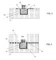
- FIG. 1shows a structure 10 comprising an interlevel dielectric layer 12 .
- the interlevel dielectric layer 12can be, for example, an oxide material or other low-k dielectric material.
- a wiring structure 14is formed within the dielectric layer 12 using conventional lithography, etching and deposition processes.
- the formation of the wiring structure 14begins with the deposition and patterning of a resist on the interlevel dielectric layer 12 .
- the resistpatterned by exposure to energy (light) to form a pattern (openings), which corresponds to the dimensions of the wiring structure 14 .
- a reactive ion etching (RIE) processis performed through the resist pattern to form a trench.
- the resistcan then be removed using conventional etchants and/or stripping techniques, e.g., oxygen ashing.
- a barrier/liner material 16 ′is formed within the opening.
- the barrier/liner material 16 ′can be a combination of a barrier metal or metal alloy material and a liner metal or metal alloy material.
- the barrier/liner material 16 ′is deposited using either plasma vapor deposition (PVD), chemical vapor deposition (CVD) or atomic layer deposition (ALD) processes.
- PVDplasma vapor deposition
- CVDchemical vapor deposition
- ALDatomic layer deposition
- the PVD processprovides a dense layer of barrier/liner material 16 ′, thus providing significantly improved barrier performance due to increased barrier density.
- the copper fillwill not leak into the interlevel dielectric layer thereby preventing time-dependent dielectric breakdown TDDB.
- oxygenwill not leak into the copper fill thereby decreasing interconnect resistance and increasing via interconnect and wiring structure lifetime.
- the barrier materialcan be TaN or TiN with the liner material being Ta or Ti, respectively, or Co.
- a seed layeris deposited on the barrier/liner material 16 ′ followed by a deposition of wiring metal to form the wiring structure 14 .
- a seed layer of coppercan be deposited using a PVD process, followed by an electroplating of copper material (both of represented at reference numeral 16 ′′).
- other metal materialscan also be used for the wiring structure 14 .
- any residual barrier/liner material 16 ′ and wiring material 16 ′′can be removed from the upper surface of the interlevel dielectric layer 12 using a chemical mechanical polishing (CMP) process.
- CMPchemical mechanical polishing
- the CMP processwill also planarize the wiring structure 14 and the interlevel dielectric layer 12 , for subsequent processing.
- FIG. 2 ashows a cross sectional view of a structure and respective processing steps in accordance with aspects of the present invention
- FIG. 2 bshows a top down view of the structure of FIG. 2 a
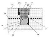
- a cap layer 18is shown deposited on the planarized surface of the wiring structure 14 and the interlevel dielectric layer 12 .
- the cap layer 18is represented in a partial transparent view to show the underlying structures, e.g., wiring structure 14 and the interlevel dielectric layer 12 , for descriptive purposes only.
- the cap layer 18is a thin dielectric hard mask layer of, e.g., SiN or SiNC; although other capping materials are also contemplated by the present invention.
- the thin dielectric hard mask layercan have a thickness of about 25 nm or less, by way of one non-limiting illustrative example.
- the cap layer 18can be deposited using a conventional chemical vapor deposition (CVD) process.
- An opening 20is formed in the cap layer 18 using conventional lithography and etching processes, e.g., a wet etching process. As shown in FIG. 2 b , the opening 20 crosses over the wiring structure 14 in order to expose a surface thereof.
- the opening 20can be a slot pattern, crossing over a segment of the underlying wiring structure 14 to expose a portion thereof for further processing.
- the slot 20can be formed orthogonal to the underlying wiring structure 14 . In this way, subsequently formed structures, e.g., via and wiring structure, can be self-aligned with the underlying wiring structure 14 .
- the exposed surface of the wiring structure 14undergoes a cleaning process, prior to a selective CVD Co growth. More specifically, in embodiments, the exposed surface of the wiring structure 14 is cleaned with a hydrogen plasma process to remove any oxide that formed on the surface of the wiring structure 14 when exposed to air, e.g., after the wet etching process. After the cleaning process to remove oxide, a selective CVD Co growth process overfills the opening 20 , which is in direct electrical contact with the exposed metal surface of the wiring structure 14 . The selective CVD Co growth process will overfill the opening 20 , forming a self-aligned inverted via interconnect structure 22 . In embodiments, the selective CVD Co growth will not nucleate on the interlevel dielectric layer 12 or the cap layer 18 .
- the structuree.g., self-aligned inverted via interconnect structure 22 and underlying metal wiring structure, will exhibit decreased contact resistance.
- the self-aligned inverted via interconnect structure 22can be used to prevent electromigration, e.g., the transport of material caused by the gradual movement of ions in a conductor due to the momentum transfer between conducting electrons and diffusing metal atoms.
- the self-aligned inverted via interconnect structure 22can prevent two types of failure modes for via interconnect structures and wiring structures: (i) via depletion; and (ii) line depletion.
- Via depletionoccurs when electrons flow from a wiring line below into the via interconnect structure above.
- line depletionoccurs when electrons flow from the via interconnect structure down to the wiring line below.
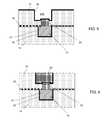
- an interlevel dielectric material 24is deposited on the self-aligned inverted via interconnect structure 22 and the cap layer 18 .
- the interlevel dielectric material 24can be an oxide material deposited using a conventional CVD process.
- An opening (trench) 24 ais formed in the interlevel dielectric material 24 , exposing one or more surfaces of the self-aligned inverted via interconnect structure 22 .
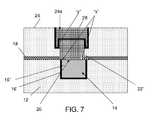
- the opening (trench) 24 acan be formed at different depths, exposing more or less surface area of the self-aligned inverted via interconnect structure 22 as shown representatively in both FIG. 4 and FIG. 7 , in order to adjust the surface contact resistance between the self-aligned inverted via interconnect structure 22 and an upper wiring structure.
- the opening (trench) 24 ais formed using conventional lithography and etching processes, as described herein.
- barrier/liner material 26is formed on the surfaces of the interlevel dielectric material 24 , in addition to any exposed surfaces of the self-aligned inverted via interconnect structure 22 within the opening (trench) 24 a .
- the barrier/liner material 26can be a combination of a barrier material and a liner material.
- the barrier materialcan be TaN or TiN with the liner material being Ta, Ti or Co, respectively.
- the barrier/liner material 26can be deposited on exposed surfaces of the self-aligned inverted via interconnect structure 22 and surfaces of the interlevel dielectric material 24 (including sidewalls of the opening (trench) 24 a , using a conventional PVD process.
- an upper wiring structure 28is formed in direct contact with the barrier/liner material 26 and hence in electrical contact with the self-aligned inverted via interconnect structure 22 within the opening (trench) 24 a .
- the upper wiring structure 28is formed by a deposition of a seed layer, followed by an electroplating process for the remaining portions of the wiring structure 28 .
- a seed layer of copperis deposited using a PVD process, followed by an electroplating of copper material (both represented at reference numeral 28 ).
- other metal materialscan also be used for the upper wiring structure 28 .
- Any residual barrier/liner material 26 and wiring material of the wiring structure 28can be removed from the upper surface of the interlevel dielectric layer 24 using a chemical mechanical polishing (CMP) process.
- CMPchemical mechanical polishing
- the CMP processwill also planarize the material of the wiring structure 28 and the interlevel dielectric layer 24 , for subsequent processing.
- the upper wiring structure 28is self-aligned with the self-aligned inverted via interconnect structure 22 , with an increased contact surface area (compared to conventional structures).
- This increased contact surface areawill reduce the interfacial resistance with the upper wiring structure 28 (i.e., an inverted via-gouging approach).
- the barrier/liner material 26 at the interface between the wiring structure 28 and the self-aligned inverted via interconnect structure 22will minimize electromigration.
- the surface contact areascan be adjusted by forming a deeper opening (trench) 24 a as described with respect to FIG. 7 .
- FIG. 7shows an alternative structure and respective fabrication processes in accordance with aspects of the invention.
- the self-aligned inverted via interconnect structure 22 ′is shown to be overgrown, e.g., larger than the opening 20 .
- the self-aligned inverted via interconnect structure 22 ′can be formed by a lateral overgrowth of the cobalt onto edges of the opening 20 , on the cap layer 18 , e.g., the cobalt overlaps onto the cap layer 18 by “x” distance on one or both sides.
- distance “x”can equal any overlap of the upper wiring structure 28 , thereby effectively increasing the contact area between the self-aligned inverted via interconnect structure 22 ′ and the upper wiring structure 28 . This increased contact surface area, in turn, will decrease the contact resistance of the structure.
- a contact area between the wiring structure 28 and the self-aligned inverted via interconnect structure 22can be increased.
- the opening 24 acan be deeper than shown in FIG. 6 , for example, to expose more surface area of the self-aligned inverted via interconnect structure 22 ′ (as represented by dimension “y”).
- This deeper opening 24 awill also effectively increase the contact surface area between the self-aligned inverted via interconnect structure 22 ′ and the upper wiring structure 28 , hence decreasing the resistance of the structure (i.e., inverted via-gouging).
- the method(s) as described aboveis used in the fabrication of integrated circuit chips.
- the resulting integrated circuit chipscan be distributed by the fabricator in raw wafer form (that is, as a single wafer that has multiple unpackaged chips), as a bare die, or in a packaged form.
- the chipis mounted in a single chip package (such as a plastic carrier, with leads that are affixed to a motherboard or other higher level carrier) or in a multichip package (such as a ceramic carrier that has either or both surface interconnections or buried interconnections).
- the chipis then integrated with other chips, discrete circuit elements, and/or other signal processing devices as part of either (a) an intermediate product, such as a motherboard, or (b) an end product.
- the end productcan be any product that includes integrated circuit chips, ranging from toys and other low-end applications to advanced computer products having a display, a keyboard or other input device, and a central processor.
Landscapes
- Engineering & Computer Science (AREA)
- Physics & Mathematics (AREA)
- Microelectronics & Electronic Packaging (AREA)
- General Physics & Mathematics (AREA)
- Computer Hardware Design (AREA)
- Condensed Matter Physics & Semiconductors (AREA)
- Power Engineering (AREA)
- Manufacturing & Machinery (AREA)
- Chemical & Material Sciences (AREA)
- Chemical Kinetics & Catalysis (AREA)
- General Chemical & Material Sciences (AREA)
- Inorganic Chemistry (AREA)
- Geometry (AREA)
- Internal Circuitry In Semiconductor Integrated Circuit Devices (AREA)
Abstract
Description
- The invention relates to semiconductor structures and, more particularly, to self-aligned via interconnect structures and methods of manufacturing thereof.
- Scaling of semiconductor devices is becoming ever more difficult in sub-22 nm technologies. For example, as structures continue to scale downward, via contact resistance becomes a performance limiting factor; that is, the via contact resistance becomes very high, particularly in back end of the line (BEOL) via interconnect structures.
- By way of example, dual-damascene fill processes require PVD liner/barrier deposition. Due to the line width requirements in scaled technologies, e.g.,
sub 22 nm, the liner/barrier deposition will displace the primary conductor. As the PVD liner/barrier materials, e.g., TaN and Ta, have higher resistance than the primary conductors, e.g., Cu, dual-damascene fill processes have become a major contributor to increased contact resistance. This increased contact resistance, in turn, leads to decreased performance of the semiconductor device. - Also, as process technologies continue to shrink towards 14-nanometers (nm) and beyond, it is becoming difficult to build self-aligned fine pitch vias with current lithography processes. This is mainly due to the size of the underlying wiring lines, e.g., width of the underling wiring structure, as well as current capabilities of lithography tool optics for 32 nm and smaller dimension technologies.
- In an aspect of the invention, a method includes forming a wiring structure in a dielectric material. The method further includes forming a cap layer over a surface of the wiring structure and the dielectric material. The method further includes forming an opening in the cap layer to expose a portion of the wiring structure. The method further includes selectively growing a metal or metal-alloy via interconnect structure material on the exposed portion of the wiring structure, through the opening in the cap layer. The method further includes forming an upper wiring structure in electrical contact with the metal or metal-alloy via interconnect structure.
- In an aspect of the invention, a method includes: forming a wiring structure within a dielectric material; forming a dielectric masking layer over the wiring structure and the dielectric material; forming an opening in the dielectric masking layer, exposing a portion of the wiring structure; overfilling the opening with metal or metal-alloy material to form a via interconnect structure in direct electrical contact with the wiring structure; and forming an upper wiring structure in electrical contact with the via interconnect structure, within a trench formed in an upper dielectric material.
- In an aspect of the invention, a method includes: forming a wiring structure in a dielectric layer; depositing a dielectric cap layer over the wiring structure and the dielectric layer; etching an opening in the dielectric layer, exposing a surface of the wiring structure; forming a self-aligned via interconnect structure in direct electrical contact with the metal material of the wiring structure by overfilling the opening with a metal or metal-alloy growth process; depositing an interlevel dielectric material over the self-aligned via interconnect structure and the dielectric cap layer; etching a trench within the interlevel dielectric material to expose one or more surfaces of the self-aligned via interconnect structure; depositing a barrier material and liner material over the exposed one or more surfaces of the self-aligned via interconnect structure and on sidewalls of the trench; and electroplating a metal or metal-alloy material on the liner material to complete formation of an upper wiring structure, in electrical contact with the via interconnect structure.
- In an aspect of the invention, a structure includes a self-aligned cobalt interconnect structure between and in electrical contact with an upper wiring layer and a lower wiring layer. The self-aligned cobalt interconnect structure is an overgrowth of cobalt within an opening of a dielectric cap material on the lower wiring layer.
- The present invention is described in the detailed description which follows, in reference to the noted plurality of drawings by way of non-limiting examples of exemplary embodiments of the present invention.
FIGS. 1, 2 aand2b-6 show structures and respective processing steps in accordance with aspects of the present invention; andFIG. 7 shows an alternative structure and respective processing steps in accordance with aspects of the present invention.- The invention relates to semiconductor structures and, more particularly, to self-aligned via interconnect structures and methods of manufacturing thereof. More specifically, the present invention relates to self-aligned inverted via interconnect structures formed with selective CVD cobalt processes, which are self-aligned to underlying metal wiring structures. In embodiments, the self-aligned inverted via interconnect, e.g., cobalt via, is formed between an upper copper wiring structure and a lower copper wiring structure; although, other materials are also contemplated for use with the wiring structures. In embodiments, the self-aligned inverted via interconnect structure can be deposited by a selective metal growth process formed through a via in a dielectric cap layer formed over the upper wiring structure. In embodiments, the selective metal growth process is a selective cobalt growth process, which overfills the opening in the dielectric cap layer and can even be allowed to grow laterally on the surface of the dielectric cap layer.
- In embodiments, the self-aligned inverted via interconnect structure introduces minimal interfacial resistance to the underlying wiring level. This is due to the fact that the self-aligned inverted via interconnect structure does not require a barrier material and a liner material at the interface with the underlying wiring structure. That is, by using the self-aligned inverted via interconnect structure, it is now possible to eliminate the liner/barrier interface between the via and underlying wire structure. Moreover, the self-aligned inverted via interconnect structure does not displace any primary conductive material in a via and, in fact, increases a contact area with an upper wiring structure, hence reducing the interfacial resistance with the upper wiring structure.
- The self-aligned inverted via interconnect structure can be manufactured in a number of ways using a number of different tools. In general, though, the methodologies and tools are used to form structures with dimensions in the micrometer and nanometer scale. The methodologies, i.e., technologies, employed to manufacture the optimized wires have been adopted from integrated circuit (IC) technology. For example, the structures, e.g., self-aligned inverted via interconnect structure, are built on wafers and are realized in films of material patterned by photolithographic processes on the top of a wafer. In particular, the fabrication of the self-aligned inverted via interconnect structure uses three basic building blocks: (i) deposition of thin films of material on a substrate, (ii) applying a patterned mask on top of the films by photolithographic imaging, and (iii) etching the films selectively to the mask.
FIG. 1 shows a structure and respective processing steps in accordance with aspects of the present invention. In particular,FIG. 1 shows astructure 10 comprising an interleveldielectric layer 12. In embodiments, the interleveldielectric layer 12 can be, for example, an oxide material or other low-k dielectric material. Awiring structure 14 is formed within thedielectric layer 12 using conventional lithography, etching and deposition processes. For example, the formation of thewiring structure 14 begins with the deposition and patterning of a resist on the interleveldielectric layer 12. The resist patterned by exposure to energy (light) to form a pattern (openings), which corresponds to the dimensions of thewiring structure 14. A reactive ion etching (RIE) process is performed through the resist pattern to form a trench. The resist can then be removed using conventional etchants and/or stripping techniques, e.g., oxygen ashing.- A barrier/
liner material 16′ is formed within the opening. In embodiments, the barrier/liner material 16′ can be a combination of a barrier metal or metal alloy material and a liner metal or metal alloy material. In embodiments, the barrier/liner material 16′ is deposited using either plasma vapor deposition (PVD), chemical vapor deposition (CVD) or atomic layer deposition (ALD) processes. The PVD process provides a dense layer of barrier/liner material 16′, thus providing significantly improved barrier performance due to increased barrier density. Specifically, compared to CVD or ALD processes, in PVD processes, the copper fill will not leak into the interlevel dielectric layer thereby preventing time-dependent dielectric breakdown TDDB. Also, due to the increased barrier density, oxygen will not leak into the copper fill thereby decreasing interconnect resistance and increasing via interconnect and wiring structure lifetime. - In embodiments, the barrier material can be TaN or TiN with the liner material being Ta or Ti, respectively, or Co. A seed layer is deposited on the barrier/
liner material 16′ followed by a deposition of wiring metal to form thewiring structure 14. By way of example, a seed layer of copper can be deposited using a PVD process, followed by an electroplating of copper material (both of represented atreference numeral 16″). In embodiments, other metal materials can also be used for thewiring structure 14. - Still referring to
FIG. 1 , any residual barrier/liner material 16′ andwiring material 16″ can be removed from the upper surface of the interleveldielectric layer 12 using a chemical mechanical polishing (CMP) process. The CMP process will also planarize thewiring structure 14 and the interleveldielectric layer 12, for subsequent processing. FIG. 2a shows a cross sectional view of a structure and respective processing steps in accordance with aspects of the present invention; whereas,FIG. 2b shows a top down view of the structure ofFIG. 2a . In both of these views, acap layer 18 is shown deposited on the planarized surface of thewiring structure 14 and the interleveldielectric layer 12. InFIG. 2b , thecap layer 18 is represented in a partial transparent view to show the underlying structures, e.g.,wiring structure 14 and the interleveldielectric layer 12, for descriptive purposes only.- In embodiments, the
cap layer 18 is a thin dielectric hard mask layer of, e.g., SiN or SiNC; although other capping materials are also contemplated by the present invention. The thin dielectric hard mask layer can have a thickness of about 25 nm or less, by way of one non-limiting illustrative example. In embodiments, thecap layer 18 can be deposited using a conventional chemical vapor deposition (CVD) process. Anopening 20 is formed in thecap layer 18 using conventional lithography and etching processes, e.g., a wet etching process. As shown inFIG. 2b , theopening 20 crosses over thewiring structure 14 in order to expose a surface thereof. In embodiments, theopening 20 can be a slot pattern, crossing over a segment of theunderlying wiring structure 14 to expose a portion thereof for further processing. By way of further example, theslot 20 can be formed orthogonal to theunderlying wiring structure 14. In this way, subsequently formed structures, e.g., via and wiring structure, can be self-aligned with theunderlying wiring structure 14. - In
FIG. 3 , the exposed surface of thewiring structure 14 undergoes a cleaning process, prior to a selective CVD Co growth. More specifically, in embodiments, the exposed surface of thewiring structure 14 is cleaned with a hydrogen plasma process to remove any oxide that formed on the surface of thewiring structure 14 when exposed to air, e.g., after the wet etching process. After the cleaning process to remove oxide, a selective CVD Co growth process overfills theopening 20, which is in direct electrical contact with the exposed metal surface of thewiring structure 14. The selective CVD Co growth process will overfill theopening 20, forming a self-aligned inverted viainterconnect structure 22. In embodiments, the selective CVD Co growth will not nucleate on the interleveldielectric layer 12 or thecap layer 18. - By utilizing the processes described herein, it is no longer necessary to form a barrier/liner material at the interface between the
wiring structure 14 and the self-aligned inverted viainterconnect structure 22. By not using the barrier/liner material, the structure, e.g., self-aligned inverted viainterconnect structure 22 and underlying metal wiring structure, will exhibit decreased contact resistance. Also, advantageously, the self-aligned inverted viainterconnect structure 22 can be used to prevent electromigration, e.g., the transport of material caused by the gradual movement of ions in a conductor due to the momentum transfer between conducting electrons and diffusing metal atoms. In fact, the self-aligned inverted viainterconnect structure 22 can prevent two types of failure modes for via interconnect structures and wiring structures: (i) via depletion; and (ii) line depletion. Via depletion occurs when electrons flow from a wiring line below into the via interconnect structure above. On the other hand, line depletion occurs when electrons flow from the via interconnect structure down to the wiring line below. - In
FIG. 4 , an interleveldielectric material 24 is deposited on the self-aligned inverted viainterconnect structure 22 and thecap layer 18. In embodiments, the interleveldielectric material 24 can be an oxide material deposited using a conventional CVD process. An opening (trench)24ais formed in the interleveldielectric material 24, exposing one or more surfaces of the self-aligned inverted viainterconnect structure 22. Depending on the designed contact resistance, the opening (trench)24acan be formed at different depths, exposing more or less surface area of the self-aligned inverted viainterconnect structure 22 as shown representatively in bothFIG. 4 andFIG. 7 , in order to adjust the surface contact resistance between the self-aligned inverted viainterconnect structure 22 and an upper wiring structure. In embodiments, the opening (trench)24ais formed using conventional lithography and etching processes, as described herein. - In
FIG. 5 , following the formation of the opening (trench)24a, barrier/liner material 26 is formed on the surfaces of the interleveldielectric material 24, in addition to any exposed surfaces of the self-aligned inverted viainterconnect structure 22 within the opening (trench)24a. In embodiments, the barrier/liner material 26 can be a combination of a barrier material and a liner material. For example, the barrier material can be TaN or TiN with the liner material being Ta, Ti or Co, respectively. In embodiments, the barrier/liner material 26 can be deposited on exposed surfaces of the self-aligned inverted viainterconnect structure 22 and surfaces of the interlevel dielectric material24 (including sidewalls of the opening (trench)24a, using a conventional PVD process. - In
FIG. 6 , anupper wiring structure 28 is formed in direct contact with the barrier/liner material 26 and hence in electrical contact with the self-aligned inverted viainterconnect structure 22 within the opening (trench)24a. In embodiments, theupper wiring structure 28 is formed by a deposition of a seed layer, followed by an electroplating process for the remaining portions of thewiring structure 28. By way of more specific example, a seed layer of copper is deposited using a PVD process, followed by an electroplating of copper material (both represented at reference numeral28). In embodiments, other metal materials can also be used for theupper wiring structure 28. Any residual barrier/liner material 26 and wiring material of thewiring structure 28 can be removed from the upper surface of the interleveldielectric layer 24 using a chemical mechanical polishing (CMP) process. The CMP process will also planarize the material of thewiring structure 28 and the interleveldielectric layer 24, for subsequent processing. - In this way, the
upper wiring structure 28 is self-aligned with the self-aligned inverted viainterconnect structure 22, with an increased contact surface area (compared to conventional structures). This increased contact surface area will reduce the interfacial resistance with the upper wiring structure28 (i.e., an inverted via-gouging approach). Also, the barrier/liner material 26 at the interface between thewiring structure 28 and the self-aligned inverted viainterconnect structure 22 will minimize electromigration. Moreover, the surface contact areas can be adjusted by forming a deeper opening (trench)24aas described with respect toFIG. 7 . FIG. 7 shows an alternative structure and respective fabrication processes in accordance with aspects of the invention. InFIG. 7 , the self-aligned inverted viainterconnect structure 22′ is shown to be overgrown, e.g., larger than theopening 20. For example, the self-aligned inverted viainterconnect structure 22′ can be formed by a lateral overgrowth of the cobalt onto edges of theopening 20, on thecap layer 18, e.g., the cobalt overlaps onto thecap layer 18 by “x” distance on one or both sides. In embodiments, distance “x” can equal any overlap of theupper wiring structure 28, thereby effectively increasing the contact area between the self-aligned inverted viainterconnect structure 22′ and theupper wiring structure 28. This increased contact surface area, in turn, will decrease the contact resistance of the structure.- Also, by adjusting the depth of the opening (trench)24a, a contact area between the
wiring structure 28 and the self-aligned inverted viainterconnect structure 22 can be increased. For example, as further shown inFIG. 7 , the opening24acan be deeper than shown inFIG. 6 , for example, to expose more surface area of the self-aligned inverted viainterconnect structure 22′ (as represented by dimension “y”). Thisdeeper opening 24awill also effectively increase the contact surface area between the self-aligned inverted viainterconnect structure 22′ and theupper wiring structure 28, hence decreasing the resistance of the structure (i.e., inverted via-gouging). - The method(s) as described above is used in the fabrication of integrated circuit chips. The resulting integrated circuit chips can be distributed by the fabricator in raw wafer form (that is, as a single wafer that has multiple unpackaged chips), as a bare die, or in a packaged form. In the latter case the chip is mounted in a single chip package (such as a plastic carrier, with leads that are affixed to a motherboard or other higher level carrier) or in a multichip package (such as a ceramic carrier that has either or both surface interconnections or buried interconnections). In any case the chip is then integrated with other chips, discrete circuit elements, and/or other signal processing devices as part of either (a) an intermediate product, such as a motherboard, or (b) an end product. The end product can be any product that includes integrated circuit chips, ranging from toys and other low-end applications to advanced computer products having a display, a keyboard or other input device, and a central processor.
- The descriptions of the various embodiments of the present invention have been presented for purposes of illustration, but are not intended to be exhaustive or limited to the embodiments disclosed. Many modifications and variations will be apparent to those of ordinary skill in the art without departing from the scope and spirit of the described embodiments. The terminology used herein was chosen to best explain the principles of the embodiments, the practical application or technical improvement over technologies found in the marketplace, or to enable others of ordinary skill in the art to understand the embodiments disclosed herein.
Claims (14)
1. A method, comprising:
forming a wiring structure in a dielectric layer;
depositing a dielectric cap layer over the wiring structure and the dielectric layer;
etching an opening in the dielectric layer, exposing a surface of the wiring structure;
forming a self-aligned via interconnect structure in direct electrical contact with the metal material of the wiring structure by overfilling the opening larger than the opening with a metal or metal-alloy growth process;
depositing an interlevel dielectric material over the self-aligned via interconnect structure and the dielectric cap layer;
etching a trench within the interlevel dielectric material to expose one or more surfaces of the self-aligned via interconnect structure;
depositing a barrier material and liner material over the exposed one or more surfaces of the self-aligned via interconnect structure and on sidewalls of the trench; and
electroplating a metal or metal-alloy material on the liner material to complete formation of an upper wiring structure, in electrical contact with the via interconnect structure.
2. The method ofclaim 1 , wherein the metal or metal-alloy growth process is a selective cobalt growth process which overfills the opening.
3. The method ofclaim 1 , wherein the selective cobalt growth process laterally overgrows onto edges of the opening.
4. The method ofclaim 3 , wherein the selective cobalt growth process forms the self-aligned via interconnect structure onto a surface of the dielectric cap layer18.
5. The method ofclaim 4 , wherein the self-aligned via interconnect structure is cobalt.
6. The method ofclaim 5 , wherein the upper wiring structure is formed to overlap the self-aligned via interconnect structure by “x” distance on one side.
7. The method ofclaim 5 , wherein the upper wiring structure is formed to overlap the self-aligned via interconnect structure by “x” distance on both sides.
8. The method ofclaim 7 , wherein the “x” distance is an equal overlap of the upper wiring structure
9. The method ofclaim 1 , wherein an interface between the self-aligned via interconnect structure and the wiring structure is devoid of a liner material and a barrier material.
10. The method ofclaim 1 , wherein the etching of the trench within the interlevel dielectric material extends beyond an upper portion of the self-aligned via interconnect structure.
11. The method ofclaim 1 , wherein the forming of the dielectric cap layer is a deposition of dielectric masking material.
12. The method ofclaim 1 , wherein the forming of the opening in the dielectric cap layer comprises forming a slot exposing the portion of the wiring structure.
13. The method ofclaim 12 , wherein the slot is formed orthogonal to the wiring structure.
14. The method ofclaim 1 , wherein an interface between the metal or metal-alloy via interconnect structure and the wiring structure is devoid of a barrier material and liner material.
Priority Applications (2)
| Application Number | Priority Date | Filing Date | Title |
|---|---|---|---|
| US15/070,242US10395984B2 (en) | 2014-12-08 | 2016-03-15 | Self-aligned via interconnect structures |
| US16/460,250US11348832B2 (en) | 2014-12-08 | 2019-07-02 | Self-aligned via interconnect structures |
Applications Claiming Priority (2)
| Application Number | Priority Date | Filing Date | Title |
|---|---|---|---|
| US14/563,554US10727122B2 (en) | 2014-12-08 | 2014-12-08 | Self-aligned via interconnect structures |
| US15/070,242US10395984B2 (en) | 2014-12-08 | 2016-03-15 | Self-aligned via interconnect structures |
Related Parent Applications (1)
| Application Number | Title | Priority Date | Filing Date |
|---|---|---|---|
| US14/563,554DivisionUS10727122B2 (en) | 2014-12-08 | 2014-12-08 | Self-aligned via interconnect structures |
Related Child Applications (1)
| Application Number | Title | Priority Date | Filing Date |
|---|---|---|---|
| US16/460,250ContinuationUS11348832B2 (en) | 2014-12-08 | 2019-07-02 | Self-aligned via interconnect structures |
Publications (2)
| Publication Number | Publication Date |
|---|---|
| US20160197013A1true US20160197013A1 (en) | 2016-07-07 |
| US10395984B2 US10395984B2 (en) | 2019-08-27 |
Family
ID=56094969
Family Applications (4)
| Application Number | Title | Priority Date | Filing Date |
|---|---|---|---|
| US14/563,554Expired - Fee RelatedUS10727122B2 (en) | 2014-12-08 | 2014-12-08 | Self-aligned via interconnect structures |
| US15/070,231AbandonedUS20160197038A1 (en) | 2014-12-08 | 2016-03-15 | Self-aligned via interconnect structures |
| US15/070,242ActiveUS10395984B2 (en) | 2014-12-08 | 2016-03-15 | Self-aligned via interconnect structures |
| US16/460,250ActiveUS11348832B2 (en) | 2014-12-08 | 2019-07-02 | Self-aligned via interconnect structures |
Family Applications Before (2)
| Application Number | Title | Priority Date | Filing Date |
|---|---|---|---|
| US14/563,554Expired - Fee RelatedUS10727122B2 (en) | 2014-12-08 | 2014-12-08 | Self-aligned via interconnect structures |
| US15/070,231AbandonedUS20160197038A1 (en) | 2014-12-08 | 2016-03-15 | Self-aligned via interconnect structures |
Family Applications After (1)
| Application Number | Title | Priority Date | Filing Date |
|---|---|---|---|
| US16/460,250ActiveUS11348832B2 (en) | 2014-12-08 | 2019-07-02 | Self-aligned via interconnect structures |
Country Status (1)
| Country | Link |
|---|---|
| US (4) | US10727122B2 (en) |
Cited By (7)
| Publication number | Priority date | Publication date | Assignee | Title |
|---|---|---|---|---|
| WO2019066855A1 (en)* | 2017-09-28 | 2019-04-04 | Intel Corporation | Interconnects having a portion without a liner material and related structures, devices, and methods |
| US10727122B2 (en) | 2014-12-08 | 2020-07-28 | International Business Machines Corporation | Self-aligned via interconnect structures |
| CN112309964A (en)* | 2019-07-31 | 2021-02-02 | 台湾积体电路制造股份有限公司 | Semiconductor device structure and forming method thereof |
| US11393753B2 (en) | 2019-11-27 | 2022-07-19 | Samsung Electronics Co., Ltd. | Interconnection structure of integrated circuit semiconductor device |
| WO2023066279A1 (en)* | 2021-10-20 | 2023-04-27 | 京东方科技集团股份有限公司 | Display substrate and display device |
| US20230144050A1 (en)* | 2021-11-05 | 2023-05-11 | International Business Machines Corporation | Phase change memory with encapsulated phase change element |
| EP4307356A4 (en)* | 2021-04-28 | 2025-01-08 | Changxin Memory Technologies, Inc. | SEMICONDUCTOR STRUCTURE AND MANUFACTURING METHODS |
Families Citing this family (62)
| Publication number | Priority date | Publication date | Assignee | Title |
|---|---|---|---|---|
| US9799555B1 (en)* | 2016-06-07 | 2017-10-24 | Globalfoundries Inc. | Cobalt interconnects covered by a metal cap |
| TWI729457B (en) | 2016-06-14 | 2021-06-01 | 美商應用材料股份有限公司 | Oxidative volumetric expansion of metals and metal containing compounds |
| US9768063B1 (en)* | 2016-06-30 | 2017-09-19 | Lam Research Corporation | Dual damascene fill |
| US10573522B2 (en) | 2016-08-16 | 2020-02-25 | Lam Research Corporation | Method for preventing line bending during metal fill process |
| US10083834B2 (en)* | 2016-09-30 | 2018-09-25 | Applied Materials, Inc. | Methods of forming self-aligned vias |
| TWI719262B (en) | 2016-11-03 | 2021-02-21 | 美商應用材料股份有限公司 | Deposition and treatment of films for patterning |
| TWI687978B (en) | 2016-11-08 | 2020-03-11 | 美商應用材料股份有限公司 | Geometric control of bottom-up pillars for patterning applications |
| US20180138123A1 (en) | 2016-11-15 | 2018-05-17 | Globalfoundries Inc. | Interconnect structure and method of forming the same |
| DE112016007569T5 (en)* | 2016-12-30 | 2019-11-28 | Intel Corporation | SELF-ADJUSTED HARD MASKS WITH CONVERTED LINERS |
| TW201839897A (en) | 2017-02-22 | 2018-11-01 | 美商應用材料股份有限公司 | Critical dimension control for self-aligned contact patterning |
| US10424507B2 (en) | 2017-04-04 | 2019-09-24 | Mirocmaterials LLC | Fully self-aligned via |
| WO2018200212A1 (en) | 2017-04-25 | 2018-11-01 | Applied Materials, Inc. | Selective deposition of tungsten for simplified process flow of tungsten oxide pillar formation |
| US10840186B2 (en) | 2017-06-10 | 2020-11-17 | Applied Materials, Inc. | Methods of forming self-aligned vias and air gaps |
| TW201906035A (en)* | 2017-06-24 | 2019-02-01 | 美商微材料有限責任公司 | Method of producing fully self-aligned vias and contacts |
| US10510602B2 (en) | 2017-08-31 | 2019-12-17 | Mirocmaterials LLC | Methods of producing self-aligned vias |
| WO2019046402A1 (en) | 2017-08-31 | 2019-03-07 | Micromaterials Llc | Methods of producing self-aligned grown via |
| US10600688B2 (en) | 2017-09-06 | 2020-03-24 | Micromaterials Llc | Methods of producing self-aligned vias |
| TWI723282B (en) | 2017-09-16 | 2021-04-01 | 美商應用材料股份有限公司 | Volumetric expansion of metal-containing films by silicidation |
| US11031285B2 (en)* | 2017-10-06 | 2021-06-08 | Invensas Bonding Technologies, Inc. | Diffusion barrier collar for interconnects |
| CN110034017A (en) | 2017-12-07 | 2019-07-19 | 微材料有限责任公司 | Method for making metal and barrier layer-liner controllably be recessed |
| EP3499557A1 (en) | 2017-12-15 | 2019-06-19 | Micromaterials LLC | Selectively etched self-aligned via processes |
| US10340183B1 (en)* | 2018-01-02 | 2019-07-02 | Globalfoundries Inc. | Cobalt plated via integration scheme |
| US10741497B2 (en) | 2018-02-15 | 2020-08-11 | Globalfoundries Inc. | Contact and interconnect structures |
| KR20190104902A (en) | 2018-03-02 | 2019-09-11 | 마이크로머티어리얼즈 엘엘씨 | Methods for removing metal oxides |
| TW202002219A (en)* | 2018-05-08 | 2020-01-01 | 美商微材料有限責任公司 | Selective removal process to create high aspect ratio fully self-aligned via |
| TW202011547A (en) | 2018-05-16 | 2020-03-16 | 美商微材料有限責任公司 | A method for creating a fully self-aligned via |
| TW202011523A (en)* | 2018-05-16 | 2020-03-16 | 美商微材料有限責任公司 | Method for increasing the verticality of pillars |
| US10395986B1 (en)* | 2018-05-30 | 2019-08-27 | International Business Machines Corporation | Fully aligned via employing selective metal deposition |
| WO2019236350A1 (en)* | 2018-06-08 | 2019-12-12 | Micromaterials Llc | A method for creating a fully self-aligned via |
| CN110660775A (en)* | 2018-06-28 | 2020-01-07 | 晟碟信息科技(上海)有限公司 | Semiconductor device including through-hole in mold pillar |
| US10636737B2 (en)* | 2018-08-21 | 2020-04-28 | Qualcomm Incorporated | Structure and method of metal wraparound for low via resistance |
| KR102661847B1 (en)* | 2018-09-11 | 2024-04-30 | 삼성전자주식회사 | Semiconductor device |
| US11380581B2 (en)* | 2018-11-09 | 2022-07-05 | Globalfoundries U.S. Inc. | Interconnect structures of semiconductor devices having a via structure through an upper conductive line |
| US12148623B2 (en)* | 2018-11-19 | 2024-11-19 | Lam Research Corporation | Deposition of tungsten on molybdenum templates |
| US11101175B2 (en) | 2018-11-21 | 2021-08-24 | International Business Machines Corporation | Tall trenches for via chamferless and self forming barrier |
| CN113366144B (en) | 2019-01-28 | 2023-07-07 | 朗姆研究公司 | Deposition of metal films |
| US10832947B2 (en) | 2019-02-28 | 2020-11-10 | International Business Machines Corporation | Fully aligned via formation without metal recessing |
| US10903117B2 (en) | 2019-03-04 | 2021-01-26 | International Business Machines Corporation | Fabricating vias with lower resistance |
| WO2020178973A1 (en)* | 2019-03-05 | 2020-09-10 | 株式会社Kokusai Electric | Method for producing semiconductor device, substrate processing apparatus and program |
| US11164938B2 (en) | 2019-03-26 | 2021-11-02 | Micromaterials Llc | DRAM capacitor module |
| WO2021046058A1 (en) | 2019-09-03 | 2021-03-11 | Lam Research Corporation | Molybdenum deposition |
| US11276637B2 (en)* | 2019-09-17 | 2022-03-15 | Taiwan Semiconductor Manufacturing Co., Ltd. | Barrier-free interconnect structure and manufacturing method thereof |
| US11437274B2 (en) | 2019-09-25 | 2022-09-06 | Micromaterials Llc | Fully self-aligned via |
| US11244859B2 (en) | 2019-10-10 | 2022-02-08 | International Business Machines Corporation | Interconnects having a via-to-line spacer for preventing short circuit events between a conductive via and an adjacent line |
| US12327762B2 (en) | 2019-10-15 | 2025-06-10 | Lam Research Corporation | Molybdenum fill |
| US11139201B2 (en) | 2019-11-04 | 2021-10-05 | International Business Machines Corporation | Top via with hybrid metallization |
| US11424185B2 (en) | 2019-12-30 | 2022-08-23 | Taiwan Semiconductor Manufacturing Co., Ltd. | Semiconductor device and manufacturing method thereof |
| US11239418B2 (en)* | 2020-01-06 | 2022-02-01 | International Business Machines Corporation | Memory device having a ring heater |
| US11205591B2 (en) | 2020-01-09 | 2021-12-21 | International Business Machines Corporation | Top via interconnect with self-aligned barrier layer |
| US11152257B2 (en) | 2020-01-16 | 2021-10-19 | International Business Machines Corporation | Barrier-less prefilled via formation |
| US11239278B2 (en) | 2020-02-04 | 2022-02-01 | International Business Machines Corporation | Bottom conductive structure with a limited top contact area |
| US11244854B2 (en) | 2020-03-24 | 2022-02-08 | International Business Machines Corporation | Dual damascene fully aligned via in interconnects |
| US11183455B2 (en) | 2020-04-15 | 2021-11-23 | International Business Machines Corporation | Interconnects with enlarged contact area |
| US11244853B2 (en) | 2020-04-23 | 2022-02-08 | International Business Machines Corporation | Fully aligned via interconnects with partially removed etch stop layer |
| CN113161321B (en)* | 2020-04-28 | 2024-10-15 | 台湾积体电路制造股份有限公司 | Semiconductor structure and method for forming semiconductor structure |
| US11398385B2 (en)* | 2020-05-08 | 2022-07-26 | Taiwan Semiconductor Manufacturing Company, Ltd. | Semiconductor device and method |
| US11361987B2 (en) | 2020-05-14 | 2022-06-14 | International Business Machines Corporation | Forming decoupled interconnects |
| US12051643B2 (en)* | 2020-05-19 | 2024-07-30 | Taiwan Semiconductor Manufacturing Company Limited | Hybrid via interconnect structure |
| US11658041B2 (en)* | 2020-05-28 | 2023-05-23 | Applied Materials, Inc. | Methods of modifying portions of layer stacks |
| JP7661711B2 (en)* | 2021-02-05 | 2025-04-15 | 富士電機株式会社 | Silicon carbide semiconductor device |
| KR20230014496A (en) | 2021-07-21 | 2023-01-30 | 삼성전자주식회사 | Semiconductor device |
| US12431431B2 (en)* | 2022-06-01 | 2025-09-30 | Taiwan Semiconductor Manufacturing Company, Ltd. | Conductive structure interconnects with downward projections |
Citations (23)
| Publication number | Priority date | Publication date | Assignee | Title |
|---|---|---|---|---|
| US20010045662A1 (en)* | 1999-05-25 | 2001-11-29 | Kabushiki Kaisha Toshiba | Semiconductor device and method for manufacturing the same |
| US20020013045A1 (en)* | 1998-07-07 | 2002-01-31 | Roger Palmans | Method for forming copper-containing metal studs |
| US20020058405A1 (en)* | 2000-08-31 | 2002-05-16 | Ying Huang | A structure to reduce line-line capacitance with low k material |
| US20020106887A1 (en)* | 2001-02-02 | 2002-08-08 | Ching-Yu Chang | Method of forming a dual damascene structure by patterning a sacrificial layer to define the plug portions of the structure |
| US20030008497A1 (en)* | 2001-07-03 | 2003-01-09 | Taiwan Semiconductor Manufacturing Co., Ltd | Thermal annealing/hydrogen containing plasma method for forming structurally stable low contact resistance damascene conductor structure |
| US6876079B2 (en)* | 2001-02-27 | 2005-04-05 | Sony Corporation | Semiconductor device and method of manufacturing the same |
| US20050170632A1 (en)* | 2003-12-31 | 2005-08-04 | Shim Sang C. | Methods of manufacturing multi-level metal lines in semiconductor devices |
| US20060211235A1 (en)* | 2005-03-17 | 2006-09-21 | Nec Electronics Corporation | Semiconductor device and manufacturing process therefor |
| US7163887B2 (en)* | 2002-02-28 | 2007-01-16 | Fujitsu Limited | Method for fabricating a semiconductor device |
| US20080061403A1 (en)* | 2006-09-08 | 2008-03-13 | Zhong-Xiang He | Dielectric layers for metal lines in semiconductor chips |
| US20080064221A1 (en)* | 2006-09-11 | 2008-03-13 | Hynix Semiconductor Inc. | Method for fabricating semiconductor device including plug |
| US20080081466A1 (en)* | 2006-09-28 | 2008-04-03 | Mie Matsuo | Method for Fabricating Semiconductor Device |
| US20090302477A1 (en)* | 2008-06-06 | 2009-12-10 | Yakov Shor | Integrated circuit with embedded contacts |
| US20100261345A1 (en)* | 2009-04-10 | 2010-10-14 | Samsung Electronics Co., Ltd | Method of manufacturing a semiconductor device |
| US20100295188A1 (en)* | 2009-05-20 | 2010-11-25 | Hynix Semiconductor Inc. | Semiconductor device having deep contact structure and method of manufacturing the same |
| US20110042752A1 (en)* | 2009-08-20 | 2011-02-24 | Sony Corporation | Semiconductor device and method for manufacturing the same |
| US20120142188A1 (en)* | 2005-10-18 | 2012-06-07 | Taiwan Semiconductor Manufacturing Co. Ltd. | Anchored damascene structures |
| US20130043591A1 (en)* | 2011-08-17 | 2013-02-21 | International Business Machines Corporation | Tungsten metallization: structure and fabrication of same |
| US20130082393A1 (en)* | 2010-06-14 | 2013-04-04 | Renesas Electronics Corporation | Semiconductor device and method of manufacturing the same |
| US20140183738A1 (en)* | 2012-12-28 | 2014-07-03 | Christopher J. Jezewski | Cobalt based interconnects and methods of fabrication thereof |
| US20140264926A1 (en)* | 2013-03-12 | 2014-09-18 | Taiwan Semiconductor Manufacturing Company, Ltd. | Method and Apparatus for Back End of Line Semiconductor Device Processing |
| US8921150B2 (en)* | 2012-12-06 | 2014-12-30 | Taiwan Semiconductor Manufacturing Co., Ltd. | Process to achieve contact protrusion for single damascene via |
| US9397045B2 (en)* | 2014-10-16 | 2016-07-19 | Taiwan Semiconductor Manufacturing Co., Ltd | Structure and formation method of damascene structure |
Family Cites Families (116)
| Publication number | Priority date | Publication date | Assignee | Title |
|---|---|---|---|---|
| US4996133A (en) | 1987-07-31 | 1991-02-26 | Texas Instruments Incorporated | Self-aligned tungsten-filled via process and via formed thereby |
| US4764484A (en) | 1987-10-08 | 1988-08-16 | Standard Microsystems Corporation | Method for fabricating self-aligned, conformal metallization of semiconductor wafer |
| GB2233820A (en) | 1989-06-26 | 1991-01-16 | Philips Nv | Providing an electrode on a semiconductor device |
| US5904697A (en) | 1995-02-24 | 1999-05-18 | Heartport, Inc. | Devices and methods for performing a vascular anastomosis |
| US20100065963A1 (en) | 1995-05-26 | 2010-03-18 | Formfactor, Inc. | Method of wirebonding that utilizes a gas flow within a capillary from which a wire is played out |
| US5783485A (en) | 1996-07-19 | 1998-07-21 | Motorola, Inc. | Process for fabricating a metallized interconnect |
| JPH10104663A (en) | 1996-09-27 | 1998-04-24 | Semiconductor Energy Lab Co Ltd | Electrooptic device and its formation |
| US6213755B1 (en) | 1997-12-02 | 2001-04-10 | Kabushiki Kaisha Katsuron | Apparatus for manufacturing a molding continuously |
| US6316801B1 (en)* | 1998-03-04 | 2001-11-13 | Nec Corporation | Semiconductor device having capacitive element structure and multilevel interconnection structure and method of fabricating the same |
| US6452276B1 (en)* | 1998-04-30 | 2002-09-17 | International Business Machines Corporation | Ultra thin, single phase, diffusion barrier for metal conductors |
| US6406939B1 (en) | 1998-05-02 | 2002-06-18 | Charles W. C. Lin | Flip chip assembly with via interconnection |
| US6326300B1 (en)* | 1998-09-21 | 2001-12-04 | Taiwan Semiconductor Manufacturing Company | Dual damascene patterned conductor layer formation method |
| US6180523B1 (en) | 1998-10-13 | 2001-01-30 | Industrial Technology Research Institute | Copper metallization of USLI by electroless process |
| US6245670B1 (en)* | 1999-02-19 | 2001-06-12 | Advanced Micro Devices, Inc. | Method for filling a dual damascene opening having high aspect ratio to minimize electromigration failure |
| US6342733B1 (en) | 1999-07-27 | 2002-01-29 | International Business Machines Corporation | Reduced electromigration and stressed induced migration of Cu wires by surface coating |
| US7494927B2 (en) | 2000-05-15 | 2009-02-24 | Asm International N.V. | Method of growing electrical conductors |
| US6891627B1 (en) | 2000-09-20 | 2005-05-10 | Kla-Tencor Technologies Corp. | Methods and systems for determining a critical dimension and overlay of a specimen |
| KR100366635B1 (en) | 2000-11-01 | 2003-01-09 | 삼성전자 주식회사 | Metal layer of semiconductor device and manufacturing method thereof |
| US6977224B2 (en)* | 2000-12-28 | 2005-12-20 | Intel Corporation | Method of electroless introduction of interconnect structures |
| US6271084B1 (en)* | 2001-01-16 | 2001-08-07 | Taiwan Semiconductor Manufacturing Company | Method of fabricating a metal-insulator-metal (MIM), capacitor structure using a damascene process |
| US6624018B1 (en)* | 2001-04-23 | 2003-09-23 | Taiwan Semiconductor Manufacturing Company | Method of fabricating a DRAM device featuring alternate fin type capacitor structures |
| US6656785B2 (en)* | 2001-10-15 | 2003-12-02 | Taiwan Semiconductor Manufacturing Co. Ltd | MIM process for logic-based embedded RAM |
| US6888251B2 (en)* | 2002-07-01 | 2005-05-03 | International Business Machines Corporation | Metal spacer in single and dual damascene processing |
| JP2004039916A (en)* | 2002-07-04 | 2004-02-05 | Nec Electronics Corp | Semiconductor device and its manufacturing method |
| JP4343571B2 (en) | 2002-07-31 | 2009-10-14 | 株式会社ルネサステクノロジ | Manufacturing method of semiconductor device |
| JP4454242B2 (en) | 2003-03-25 | 2010-04-21 | 株式会社ルネサステクノロジ | Semiconductor device and manufacturing method thereof |
| US6958540B2 (en) | 2003-06-23 | 2005-10-25 | International Business Machines Corporation | Dual damascene interconnect structures having different materials for line and via conductors |
| JP4850392B2 (en) | 2004-02-17 | 2012-01-11 | 三洋電機株式会社 | Manufacturing method of semiconductor device |
| US7018515B2 (en) | 2004-03-24 | 2006-03-28 | Applied Materials, Inc. | Selectable dual position magnetron |
| US8003122B2 (en) | 2004-03-31 | 2011-08-23 | Cordis Corporation | Device for local and/or regional delivery employing liquid formulations of therapeutic agents |
| US7425436B2 (en) | 2004-07-30 | 2008-09-16 | Promega Corporation | Covalent tethering of functional groups to proteins and substrates therefor |
| US7476618B2 (en) | 2004-10-26 | 2009-01-13 | Asm Japan K.K. | Selective formation of metal layers in an integrated circuit |
| JP4443379B2 (en) | 2004-10-26 | 2010-03-31 | 三洋電機株式会社 | Manufacturing method of semiconductor device |
| US8133534B2 (en) | 2004-11-22 | 2012-03-13 | Wisconsin Alumni Research Foundation | Methods and compositions for forming patterns with isolated or discrete features using block copolymer materials |
| US8575021B2 (en) | 2004-11-22 | 2013-11-05 | Intermolecular, Inc. | Substrate processing including a masking layer |
| US7485967B2 (en) | 2005-03-10 | 2009-02-03 | Sanyo Electric Co., Ltd. | Semiconductor device with via hole for electric connection |
| US7335588B2 (en) | 2005-04-15 | 2008-02-26 | International Business Machines Corporation | Interconnect structure and method of fabrication of same |
| US8618221B2 (en) | 2005-10-14 | 2013-12-31 | Wisconsin Alumni Research Foundation | Directed assembly of triblock copolymers |
| US8679587B2 (en) | 2005-11-29 | 2014-03-25 | State of Oregon acting by and through the State Board of Higher Education action on Behalf of Oregon State University | Solution deposition of inorganic materials and electronic devices made comprising the inorganic materials |
| KR100671646B1 (en) | 2006-01-25 | 2007-01-19 | 삼성에스디아이 주식회사 | Organic electroluminescent display and manufacturing method thereof |
| US8585753B2 (en) | 2006-03-04 | 2013-11-19 | John James Scanlon | Fibrillated biodegradable prosthesis |
| US8481977B2 (en) | 2006-03-24 | 2013-07-09 | Goldeneye, Inc. | LED light source with thermally conductive luminescent matrix |
| US20070224235A1 (en) | 2006-03-24 | 2007-09-27 | Barron Tenney | Medical devices having nanoporous coatings for controlled therapeutic agent delivery |
| US8258057B2 (en) | 2006-03-30 | 2012-09-04 | Intel Corporation | Copper-filled trench contact for transistor performance improvement |
| US8492168B2 (en) | 2006-04-18 | 2013-07-23 | Advanced Liquid Logic Inc. | Droplet-based affinity assays |
| US8613889B2 (en) | 2006-04-13 | 2013-12-24 | Advanced Liquid Logic, Inc. | Droplet-based washing |
| US7439014B2 (en) | 2006-04-18 | 2008-10-21 | Advanced Liquid Logic, Inc. | Droplet-based surface modification and washing |
| US8189100B2 (en) | 2006-07-25 | 2012-05-29 | Qualcomm Incorporated | Mobile device with dual digital camera sensors and methods of using the same |
| US8506984B2 (en) | 2006-07-26 | 2013-08-13 | Cordis Corporation | Therapeutic agent elution control process |
| DE102006044691B4 (en) | 2006-09-22 | 2012-06-21 | Infineon Technologies Ag | Method for producing a terminal conductive structure of a component |
| US7999174B2 (en) | 2006-10-09 | 2011-08-16 | Solexel, Inc. | Solar module structures and assembly methods for three-dimensional thin-film solar cells |
| US7470619B1 (en)* | 2006-12-01 | 2008-12-30 | Hrl Laboratories, Llc | Interconnect with high aspect ratio plugged vias |
| KR100881621B1 (en)* | 2007-01-12 | 2009-02-04 | 삼성전자주식회사 | Semiconductor device and method of forming the same |
| US20080197499A1 (en) | 2007-02-15 | 2008-08-21 | International Business Machines Corporation | Structure for metal cap applications |
| US7863067B2 (en) | 2007-03-14 | 2011-01-04 | Taiwan Semiconductor Manufacturing Company, Ltd. | Silicon substrate with reduced surface roughness |
| US7898037B2 (en)* | 2007-04-18 | 2011-03-01 | Taiwan Semiconductor Manufacturing Company, Ltd. | Contact scheme for MOSFETs |
| CN101330039B (en)* | 2007-06-18 | 2010-06-09 | 中芯国际集成电路制造(上海)有限公司 | Method for eliminating load effect using through-hole plug |
| JP4874884B2 (en) | 2007-07-11 | 2012-02-15 | 株式会社東芝 | Magnetic recording element and magnetic recording apparatus |
| US7815839B2 (en) | 2007-07-25 | 2010-10-19 | United Technologies Corporation | Hybrid mandrels |
| RU2496067C2 (en) | 2007-10-19 | 2013-10-20 | Шелл Интернэшнл Рисерч Маатсхаппий Б.В. | Cryogenic treatment of gas |
| JP2009117591A (en)* | 2007-11-06 | 2009-05-28 | Panasonic Corp | Wiring structure and method for forming the same |
| US8420254B2 (en) | 2007-12-25 | 2013-04-16 | Byd Co. Ltd. | End cover assembly for an electrochemical cell |
| US7892968B2 (en)* | 2008-01-21 | 2011-02-22 | International Business Machines Corporation | Via gouging methods and related semiconductor structure |
| US7830010B2 (en) | 2008-04-03 | 2010-11-09 | International Business Machines Corporation | Surface treatment for selective metal cap applications |
| US20090260823A1 (en) | 2008-04-18 | 2009-10-22 | Robert George Prince-Wright | Mines and tunnels for use in treating subsurface hydrocarbon containing formations |
| US7956466B2 (en) | 2008-05-09 | 2011-06-07 | International Business Machines Corporation | Structure for interconnect structure containing various capping materials for electrical fuse and other related applications |
| US7875948B2 (en) | 2008-10-21 | 2011-01-25 | Jaroslav Hynecek | Backside illuminated image sensor |
| US7867891B2 (en)* | 2008-12-10 | 2011-01-11 | Intel Corporation | Dual metal interconnects for improved gap-fill, reliability, and reduced capacitance |
| US8071534B2 (en) | 2009-01-28 | 2011-12-06 | Clean Technology International Corporation | Material for facilitating thermal treatments of biological tissues and method of energy targeting leading to thermal treatment of biological tissues |
| US8203187B2 (en) | 2009-03-03 | 2012-06-19 | Macronix International Co., Ltd. | 3D memory array arranged for FN tunneling program and erase |
| US8427200B2 (en) | 2009-04-14 | 2013-04-23 | Monolithic 3D Inc. | 3D semiconductor device |
| US8058137B1 (en) | 2009-04-14 | 2011-11-15 | Monolithic 3D Inc. | Method for fabrication of a semiconductor device and structure |
| US8754533B2 (en) | 2009-04-14 | 2014-06-17 | Monolithic 3D Inc. | Monolithic three-dimensional semiconductor device and structure |
| US8669778B1 (en) | 2009-04-14 | 2014-03-11 | Monolithic 3D Inc. | Method for design and manufacturing of a 3D semiconductor device |
| US8409963B2 (en) | 2009-04-28 | 2013-04-02 | CDA Procesing Limited Liability Company | Methods of embedding thin-film capacitors into semiconductor packages using temporary carrier layers |
| US8164190B2 (en)* | 2009-06-25 | 2012-04-24 | International Business Machines Corporation | Structure of power grid for semiconductor devices and method of making the same |
| WO2011001596A1 (en) | 2009-07-03 | 2011-01-06 | シャープ株式会社 | Method for forming organic layer, method for producing organic electroluminescence element, organic electroluminescence element, and organic electroluminescence display device |
| US8148728B2 (en) | 2009-10-12 | 2012-04-03 | Monolithic 3D, Inc. | Method for fabrication of a semiconductor device and structure |
| US8742476B1 (en) | 2012-11-27 | 2014-06-03 | Monolithic 3D Inc. | Semiconductor device and structure |
| US8584703B2 (en) | 2009-12-01 | 2013-11-19 | Integenx Inc. | Device with diaphragm valve |
| US8691687B2 (en)* | 2010-01-07 | 2014-04-08 | International Business Machines Corporation | Superfilled metal contact vias for semiconductor devices |
| US8377722B2 (en) | 2010-02-10 | 2013-02-19 | International Business Machines Corporation | Methods of forming structures with a focused ion beam for use in atomic force probing and structures for use in atomic force probing |
| US8461035B1 (en) | 2010-09-30 | 2013-06-11 | Monolithic 3D Inc. | Method for fabrication of a semiconductor device and structure |
| US8492886B2 (en) | 2010-02-16 | 2013-07-23 | Monolithic 3D Inc | 3D integrated circuit with logic |
| US8541819B1 (en) | 2010-12-09 | 2013-09-24 | Monolithic 3D Inc. | Semiconductor device and structure |
| US8642416B2 (en) | 2010-07-30 | 2014-02-04 | Monolithic 3D Inc. | Method of forming three dimensional integrated circuit devices using layer transfer technique |
| US8659944B2 (en) | 2010-09-01 | 2014-02-25 | Macronix International Co., Ltd. | Memory architecture of 3D array with diode in memory string |
| US8569810B2 (en) | 2010-12-07 | 2013-10-29 | International Business Machines Corporation | Metal semiconductor alloy contact with low resistance |
| US20120153483A1 (en)* | 2010-12-20 | 2012-06-21 | Akolkar Rohan N | Barrierless single-phase interconnect |
| US8481405B2 (en) | 2010-12-24 | 2013-07-09 | Io Semiconductor, Inc. | Trap rich layer with through-silicon-vias in semiconductor devices |
| US8441038B1 (en) | 2011-01-20 | 2013-05-14 | Xilinx, Inc. | Nano relay with floating bridge |
| US8563396B2 (en) | 2011-01-29 | 2013-10-22 | International Business Machines Corporation | 3D integration method using SOI substrates and structures produced thereby |
| JP5356431B2 (en) | 2011-02-17 | 2013-12-04 | 株式会社東芝 | Magnetoresistive element, magnetic head assembly, and magnetic recording apparatus |
| US8492237B2 (en) | 2011-03-08 | 2013-07-23 | International Business Machines Corporation | Methods of fabricating a bipolar junction transistor with a self-aligned emitter and base |
| US8716863B2 (en)* | 2011-07-13 | 2014-05-06 | Taiwan Semiconductor Manufacturing Company, Ltd. | Structure and method for high performance interconnect |
| US8513738B2 (en) | 2011-07-21 | 2013-08-20 | International Business Machines Corporation | ESD field-effect transistor and integrated diffusion resistor |
| US8610099B2 (en) | 2011-08-15 | 2013-12-17 | Unity Semiconductor Corporation | Planar resistive memory integration |
| US8790966B2 (en) | 2011-10-18 | 2014-07-29 | Globalfoundries Singapore Pte. Ltd. | High voltage device |
| TW201320079A (en) | 2011-11-08 | 2013-05-16 | Ind Tech Res Inst | Nonvolatile random access memory and operation method thereof |
| US8614145B2 (en) | 2011-12-14 | 2013-12-24 | Sematech, Inc. | Through substrate via formation processing using sacrificial material |
| US8557632B1 (en) | 2012-04-09 | 2013-10-15 | Monolithic 3D Inc. | Method for fabrication of a semiconductor device and structure |
| US8652962B2 (en) | 2012-06-19 | 2014-02-18 | Taiwan Semiconductor Manufacturing Co., Ltd. | Etch damage and ESL free dual damascene metal interconnect |
| US8586473B1 (en) | 2012-06-26 | 2013-11-19 | GlobalFoundries, Inc. | Methods for fabricating integrated circuits with ruthenium-lined copper |
| US8618795B1 (en) | 2012-06-29 | 2013-12-31 | General Electric Company | Sensor assembly for use in medical position and orientation tracking |
| US8759976B2 (en) | 2012-08-09 | 2014-06-24 | International Business Machines Corporation | Structure with sub-lithographic random conductors as a physical unclonable function |
| US8669176B1 (en) | 2012-08-28 | 2014-03-11 | Globalfoundries Inc. | BEOL integration scheme for copper CMP to prevent dendrite formation |
| US8623758B1 (en) | 2012-10-22 | 2014-01-07 | Globalfoundries Inc. | Subtractive metal multi-layer barrier layer for interconnect structure |
| US8686428B1 (en) | 2012-11-16 | 2014-04-01 | Monolithic 3D Inc. | Semiconductor device and structure |
| US8574929B1 (en) | 2012-11-16 | 2013-11-05 | Monolithic 3D Inc. | Method to form a 3D semiconductor device and structure |
| US8674470B1 (en) | 2012-12-22 | 2014-03-18 | Monolithic 3D Inc. | Semiconductor device and structure |
| US9385058B1 (en) | 2012-12-29 | 2016-07-05 | Monolithic 3D Inc. | Semiconductor device and structure |
| US9312204B2 (en) | 2013-09-27 | 2016-04-12 | Intel Corporation | Methods of forming parallel wires of different metal materials through double patterning and fill techniques |
| US9123785B1 (en)* | 2014-03-10 | 2015-09-01 | Intermolecular, Inc. | Method to etch Cu/Ta/TaN selectively using dilute aqueous HF/HCI solution |
| US9219033B2 (en)* | 2014-03-21 | 2015-12-22 | Taiwan Semiconductor Manufacturing Co., Ltd. | Via pre-fill on back-end-of-the-line interconnect layer |
| US10727122B2 (en) | 2014-12-08 | 2020-07-28 | International Business Machines Corporation | Self-aligned via interconnect structures |
| US10128184B2 (en)* | 2015-07-01 | 2018-11-13 | Zhuhai Chuangfeixin Technology Co., Ltd. | Antifuse structure in via hole in interplayer dielectric |
- 2014
- 2014-12-08USUS14/563,554patent/US10727122B2/ennot_activeExpired - Fee Related
- 2016
- 2016-03-15USUS15/070,231patent/US20160197038A1/ennot_activeAbandoned
- 2016-03-15USUS15/070,242patent/US10395984B2/enactiveActive
- 2019
- 2019-07-02USUS16/460,250patent/US11348832B2/enactiveActive
Patent Citations (26)
| Publication number | Priority date | Publication date | Assignee | Title |
|---|---|---|---|---|
| US20020013045A1 (en)* | 1998-07-07 | 2002-01-31 | Roger Palmans | Method for forming copper-containing metal studs |
| US20010045662A1 (en)* | 1999-05-25 | 2001-11-29 | Kabushiki Kaisha Toshiba | Semiconductor device and method for manufacturing the same |
| US20020058405A1 (en)* | 2000-08-31 | 2002-05-16 | Ying Huang | A structure to reduce line-line capacitance with low k material |
| US20020106887A1 (en)* | 2001-02-02 | 2002-08-08 | Ching-Yu Chang | Method of forming a dual damascene structure by patterning a sacrificial layer to define the plug portions of the structure |
| US6440842B1 (en)* | 2001-02-02 | 2002-08-27 | Macronix International Co. Ltd. | Method of forming a dual damascene structure by patterning a sacrificial layer to define the plug portions of the structure |
| US6876079B2 (en)* | 2001-02-27 | 2005-04-05 | Sony Corporation | Semiconductor device and method of manufacturing the same |
| US20030008497A1 (en)* | 2001-07-03 | 2003-01-09 | Taiwan Semiconductor Manufacturing Co., Ltd | Thermal annealing/hydrogen containing plasma method for forming structurally stable low contact resistance damascene conductor structure |
| US7163887B2 (en)* | 2002-02-28 | 2007-01-16 | Fujitsu Limited | Method for fabricating a semiconductor device |
| US20050170632A1 (en)* | 2003-12-31 | 2005-08-04 | Shim Sang C. | Methods of manufacturing multi-level metal lines in semiconductor devices |
| US20060211235A1 (en)* | 2005-03-17 | 2006-09-21 | Nec Electronics Corporation | Semiconductor device and manufacturing process therefor |
| US8368220B2 (en)* | 2005-10-18 | 2013-02-05 | Taiwan Semiconductor Manufacturing Co. Ltd. | Anchored damascene structures |
| US20120142188A1 (en)* | 2005-10-18 | 2012-06-07 | Taiwan Semiconductor Manufacturing Co. Ltd. | Anchored damascene structures |
| US20080061403A1 (en)* | 2006-09-08 | 2008-03-13 | Zhong-Xiang He | Dielectric layers for metal lines in semiconductor chips |
| US20080064221A1 (en)* | 2006-09-11 | 2008-03-13 | Hynix Semiconductor Inc. | Method for fabricating semiconductor device including plug |
| US20080081466A1 (en)* | 2006-09-28 | 2008-04-03 | Mie Matsuo | Method for Fabricating Semiconductor Device |
| US20090302477A1 (en)* | 2008-06-06 | 2009-12-10 | Yakov Shor | Integrated circuit with embedded contacts |
| US20100261345A1 (en)* | 2009-04-10 | 2010-10-14 | Samsung Electronics Co., Ltd | Method of manufacturing a semiconductor device |
| US20100295188A1 (en)* | 2009-05-20 | 2010-11-25 | Hynix Semiconductor Inc. | Semiconductor device having deep contact structure and method of manufacturing the same |
| US20110042752A1 (en)* | 2009-08-20 | 2011-02-24 | Sony Corporation | Semiconductor device and method for manufacturing the same |
| US20130082393A1 (en)* | 2010-06-14 | 2013-04-04 | Renesas Electronics Corporation | Semiconductor device and method of manufacturing the same |
| US20130043591A1 (en)* | 2011-08-17 | 2013-02-21 | International Business Machines Corporation | Tungsten metallization: structure and fabrication of same |
| US8921150B2 (en)* | 2012-12-06 | 2014-12-30 | Taiwan Semiconductor Manufacturing Co., Ltd. | Process to achieve contact protrusion for single damascene via |
| US20140183738A1 (en)* | 2012-12-28 | 2014-07-03 | Christopher J. Jezewski | Cobalt based interconnects and methods of fabrication thereof |
| US9514983B2 (en)* | 2012-12-28 | 2016-12-06 | Intel Corporation | Cobalt based interconnects and methods of fabrication thereof |
| US20140264926A1 (en)* | 2013-03-12 | 2014-09-18 | Taiwan Semiconductor Manufacturing Company, Ltd. | Method and Apparatus for Back End of Line Semiconductor Device Processing |
| US9397045B2 (en)* | 2014-10-16 | 2016-07-19 | Taiwan Semiconductor Manufacturing Co., Ltd | Structure and formation method of damascene structure |
Cited By (12)
| Publication number | Priority date | Publication date | Assignee | Title |
|---|---|---|---|---|
| US10727122B2 (en) | 2014-12-08 | 2020-07-28 | International Business Machines Corporation | Self-aligned via interconnect structures |
| US11348832B2 (en) | 2014-12-08 | 2022-05-31 | International Business Machines Corporation | Self-aligned via interconnect structures |
| WO2019066855A1 (en)* | 2017-09-28 | 2019-04-04 | Intel Corporation | Interconnects having a portion without a liner material and related structures, devices, and methods |
| US11264325B2 (en) | 2017-09-28 | 2022-03-01 | Intel Corporation | Interconnects having a portion without a liner material and related structures, devices, and methods |
| US11837542B2 (en) | 2017-09-28 | 2023-12-05 | Intel Corporation | Interconnects having a portion without a liner material and related structures, devices, and methods |
| CN112309964A (en)* | 2019-07-31 | 2021-02-02 | 台湾积体电路制造股份有限公司 | Semiconductor device structure and forming method thereof |
| US11393753B2 (en) | 2019-11-27 | 2022-07-19 | Samsung Electronics Co., Ltd. | Interconnection structure of integrated circuit semiconductor device |
| US12230568B2 (en) | 2019-11-27 | 2025-02-18 | Samsung Electronics Co., Ltd. | Interconnection structure of integrated circuit semiconductor device |
| EP4307356A4 (en)* | 2021-04-28 | 2025-01-08 | Changxin Memory Technologies, Inc. | SEMICONDUCTOR STRUCTURE AND MANUFACTURING METHODS |
| WO2023066279A1 (en)* | 2021-10-20 | 2023-04-27 | 京东方科技集团股份有限公司 | Display substrate and display device |
| US20230144050A1 (en)* | 2021-11-05 | 2023-05-11 | International Business Machines Corporation | Phase change memory with encapsulated phase change element |
| US12310262B2 (en)* | 2021-11-05 | 2025-05-20 | International Business Machines Corporation | Phase change memory with encapsulated phase change element |
Also Published As
| Publication number | Publication date |
|---|---|
| US20160163587A1 (en) | 2016-06-09 |
| US11348832B2 (en) | 2022-05-31 |
| US20190326170A1 (en) | 2019-10-24 |
| US10395984B2 (en) | 2019-08-27 |
| US10727122B2 (en) | 2020-07-28 |
| US20160197038A1 (en) | 2016-07-07 |
Similar Documents
| Publication | Publication Date | Title |
|---|---|---|
| US11348832B2 (en) | Self-aligned via interconnect structures | |
| US9613861B2 (en) | Damascene wires with top via structures | |
| US10177028B1 (en) | Method for manufacturing fully aligned via structures having relaxed gapfills | |
| US10573593B2 (en) | Metal interconnects for super (skip) via integration | |
| US9805972B1 (en) | Skip via structures | |
| US10290580B2 (en) | Hybrid copper structure for advance interconnect usage | |
| US9484257B2 (en) | Semiconductor devices and methods of manufacture thereof | |
| US9502350B1 (en) | Interconnect scaling method including forming dielectric layer over subtractively etched first conductive layer and forming second conductive material on dielectric layer | |
| TW201830533A (en) | Semiconductor device with interconnect structure | |
| US11114338B2 (en) | Fully aligned via in ground rule region | |
| US11233191B2 (en) | Integrated circuits with embedded memory structures and methods for fabricating the same | |
| TW201419446A (en) | Method for forming interconnect structure of integrated circuit and semiconductor device | |
| US10833149B2 (en) | Capacitors | |
| US11881431B2 (en) | Anti-fuse with laterally extended liner | |
| US9831124B1 (en) | Interconnect structures | |
| US11315872B1 (en) | Self-aligned top via | |
| US9601432B1 (en) | Advanced metallization for damage repair |
Legal Events
| Date | Code | Title | Description |
|---|---|---|---|
| AS | Assignment | Owner name:INTERNATIONAL BUSINESS MACHINES CORPORATION, NEW Y Free format text:ASSIGNMENT OF ASSIGNORS INTEREST;ASSIGNORS:BACKES, BENJAMIN C.;COHEN, BRIAN A.;NAG, JOYEETA;AND OTHERS;SIGNING DATES FROM 20141204 TO 20141205;REEL/FRAME:037987/0765 | |
| STPP | Information on status: patent application and granting procedure in general | Free format text:FINAL REJECTION MAILED | |
| STPP | Information on status: patent application and granting procedure in general | Free format text:RESPONSE AFTER FINAL ACTION FORWARDED TO EXAMINER | |
| STPP | Information on status: patent application and granting procedure in general | Free format text:NOTICE OF ALLOWANCE MAILED -- APPLICATION RECEIVED IN OFFICE OF PUBLICATIONS | |
| STPP | Information on status: patent application and granting procedure in general | Free format text:AWAITING TC RESP., ISSUE FEE NOT PAID | |
| STPP | Information on status: patent application and granting procedure in general | Free format text:PUBLICATIONS -- ISSUE FEE PAYMENT VERIFIED | |
| STCF | Information on status: patent grant | Free format text:PATENTED CASE | |
| MAFP | Maintenance fee payment | Free format text:PAYMENT OF MAINTENANCE FEE, 4TH YEAR, LARGE ENTITY (ORIGINAL EVENT CODE: M1551); ENTITY STATUS OF PATENT OWNER: LARGE ENTITY Year of fee payment:4 |