US20160169488A1 - Printed circuit board aperture based illumination system for pattern projection - Google Patents
Printed circuit board aperture based illumination system for pattern projectionDownload PDFInfo
- Publication number
- US20160169488A1 US20160169488A1US14/567,766US201414567766AUS2016169488A1US 20160169488 A1US20160169488 A1US 20160169488A1US 201414567766 AUS201414567766 AUS 201414567766AUS 2016169488 A1US2016169488 A1US 2016169488A1
- Authority
- US
- United States
- Prior art keywords
- light
- circuit board
- printed circuit
- emitting diodes
- aperture
- Prior art date
- Legal status (The legal status is an assumption and is not a legal conclusion. Google has not performed a legal analysis and makes no representation as to the accuracy of the status listed.)
- Granted
Links
Images


Classifications
- F—MECHANICAL ENGINEERING; LIGHTING; HEATING; WEAPONS; BLASTING
- F21—LIGHTING
- F21V—FUNCTIONAL FEATURES OR DETAILS OF LIGHTING DEVICES OR SYSTEMS THEREOF; STRUCTURAL COMBINATIONS OF LIGHTING DEVICES WITH OTHER ARTICLES, NOT OTHERWISE PROVIDED FOR
- F21V19/00—Fastening of light sources or lamp holders
- F21V19/001—Fastening of light sources or lamp holders the light sources being semiconductors devices, e.g. LEDs
- F21V19/0015—Fastening arrangements intended to retain light sources
- F—MECHANICAL ENGINEERING; LIGHTING; HEATING; WEAPONS; BLASTING
- F21—LIGHTING
- F21V—FUNCTIONAL FEATURES OR DETAILS OF LIGHTING DEVICES OR SYSTEMS THEREOF; STRUCTURAL COMBINATIONS OF LIGHTING DEVICES WITH OTHER ARTICLES, NOT OTHERWISE PROVIDED FOR
- F21V11/00—Screens not covered by groups F21V1/00, F21V3/00, F21V7/00 or F21V9/00
- F21V11/08—Screens not covered by groups F21V1/00, F21V3/00, F21V7/00 or F21V9/00 using diaphragms containing one or more apertures
- F21V11/12—Screens not covered by groups F21V1/00, F21V3/00, F21V7/00 or F21V9/00 using diaphragms containing one or more apertures of slot type
- F—MECHANICAL ENGINEERING; LIGHTING; HEATING; WEAPONS; BLASTING
- F21—LIGHTING
- F21V—FUNCTIONAL FEATURES OR DETAILS OF LIGHTING DEVICES OR SYSTEMS THEREOF; STRUCTURAL COMBINATIONS OF LIGHTING DEVICES WITH OTHER ARTICLES, NOT OTHERWISE PROVIDED FOR
- F21V5/00—Refractors for light sources
- F21V5/04—Refractors for light sources of lens shape
- F21V5/048—Refractors for light sources of lens shape the lens being a simple lens adapted to cooperate with a point-like source for emitting mainly in one direction and having an axis coincident with the main light transmission direction, e.g. convergent or divergent lenses, plano-concave or plano-convex lenses
- H—ELECTRICITY
- H05—ELECTRIC TECHNIQUES NOT OTHERWISE PROVIDED FOR
- H05K—PRINTED CIRCUITS; CASINGS OR CONSTRUCTIONAL DETAILS OF ELECTRIC APPARATUS; MANUFACTURE OF ASSEMBLAGES OF ELECTRICAL COMPONENTS
- H05K1/00—Printed circuits
- H05K1/02—Details
- H05K1/0274—Optical details, e.g. printed circuits comprising integral optical means
- H—ELECTRICITY
- H05—ELECTRIC TECHNIQUES NOT OTHERWISE PROVIDED FOR
- H05K—PRINTED CIRCUITS; CASINGS OR CONSTRUCTIONAL DETAILS OF ELECTRIC APPARATUS; MANUFACTURE OF ASSEMBLAGES OF ELECTRICAL COMPONENTS
- H05K1/00—Printed circuits
- H05K1/02—Details
- H05K1/14—Structural association of two or more printed circuits
- H05K1/147—Structural association of two or more printed circuits at least one of the printed circuits being bent or folded, e.g. by using a flexible printed circuit
- H—ELECTRICITY
- H05—ELECTRIC TECHNIQUES NOT OTHERWISE PROVIDED FOR
- H05K—PRINTED CIRCUITS; CASINGS OR CONSTRUCTIONAL DETAILS OF ELECTRIC APPARATUS; MANUFACTURE OF ASSEMBLAGES OF ELECTRICAL COMPONENTS
- H05K1/00—Printed circuits
- H05K1/18—Printed circuits structurally associated with non-printed electric components
- H05K1/182—Printed circuits structurally associated with non-printed electric components associated with components mounted in the printed circuit board, e.g. insert mounted components [IMC]
- H05K1/183—Components mounted in and supported by recessed areas of the printed circuit board
- F21Y2101/02—
- F—MECHANICAL ENGINEERING; LIGHTING; HEATING; WEAPONS; BLASTING
- F21—LIGHTING
- F21Y—INDEXING SCHEME ASSOCIATED WITH SUBCLASSES F21K, F21L, F21S and F21V, RELATING TO THE FORM OR THE KIND OF THE LIGHT SOURCES OR OF THE COLOUR OF THE LIGHT EMITTED
- F21Y2115/00—Light-generating elements of semiconductor light sources
- F21Y2115/10—Light-emitting diodes [LED]
- H—ELECTRICITY
- H05—ELECTRIC TECHNIQUES NOT OTHERWISE PROVIDED FOR
- H05K—PRINTED CIRCUITS; CASINGS OR CONSTRUCTIONAL DETAILS OF ELECTRIC APPARATUS; MANUFACTURE OF ASSEMBLAGES OF ELECTRICAL COMPONENTS
- H05K2201/00—Indexing scheme relating to printed circuits covered by H05K1/00
- H05K2201/09—Shape and layout
- H05K2201/09009—Substrate related
- H05K2201/09063—Holes or slots in insulating substrate not used for electrical connections
- H—ELECTRICITY
- H05—ELECTRIC TECHNIQUES NOT OTHERWISE PROVIDED FOR
- H05K—PRINTED CIRCUITS; CASINGS OR CONSTRUCTIONAL DETAILS OF ELECTRIC APPARATUS; MANUFACTURE OF ASSEMBLAGES OF ELECTRICAL COMPONENTS
- H05K2201/00—Indexing scheme relating to printed circuits covered by H05K1/00
- H05K2201/09—Shape and layout
- H05K2201/09009—Substrate related
- H05K2201/09072—Hole or recess under component or special relationship between hole and component
- H—ELECTRICITY
- H05—ELECTRIC TECHNIQUES NOT OTHERWISE PROVIDED FOR
- H05K—PRINTED CIRCUITS; CASINGS OR CONSTRUCTIONAL DETAILS OF ELECTRIC APPARATUS; MANUFACTURE OF ASSEMBLAGES OF ELECTRICAL COMPONENTS
- H05K2201/00—Indexing scheme relating to printed circuits covered by H05K1/00
- H05K2201/09—Shape and layout
- H05K2201/09818—Shape or layout details not covered by a single group of H05K2201/09009 - H05K2201/09809
- H05K2201/09845—Stepped hole, via, edge, bump or conductor
- H—ELECTRICITY
- H05—ELECTRIC TECHNIQUES NOT OTHERWISE PROVIDED FOR
- H05K—PRINTED CIRCUITS; CASINGS OR CONSTRUCTIONAL DETAILS OF ELECTRIC APPARATUS; MANUFACTURE OF ASSEMBLAGES OF ELECTRICAL COMPONENTS
- H05K2201/00—Indexing scheme relating to printed circuits covered by H05K1/00
- H05K2201/09—Shape and layout
- H05K2201/09818—Shape or layout details not covered by a single group of H05K2201/09009 - H05K2201/09809
- H05K2201/09854—Hole or via having special cross-section, e.g. elliptical
- H—ELECTRICITY
- H05—ELECTRIC TECHNIQUES NOT OTHERWISE PROVIDED FOR
- H05K—PRINTED CIRCUITS; CASINGS OR CONSTRUCTIONAL DETAILS OF ELECTRIC APPARATUS; MANUFACTURE OF ASSEMBLAGES OF ELECTRICAL COMPONENTS
- H05K2201/00—Indexing scheme relating to printed circuits covered by H05K1/00
- H05K2201/10—Details of components or other objects attached to or integrated in a printed circuit board
- H05K2201/10007—Types of components
- H05K2201/10106—Light emitting diode [LED]
- H—ELECTRICITY
- H05—ELECTRIC TECHNIQUES NOT OTHERWISE PROVIDED FOR
- H05K—PRINTED CIRCUITS; CASINGS OR CONSTRUCTIONAL DETAILS OF ELECTRIC APPARATUS; MANUFACTURE OF ASSEMBLAGES OF ELECTRICAL COMPONENTS
- H05K2203/00—Indexing scheme relating to apparatus or processes for manufacturing printed circuits covered by H05K3/00
- H05K2203/16—Inspection; Monitoring; Aligning
- H05K2203/167—Using mechanical means for positioning, alignment or registration, e.g. using rod-in-hole alignment
- H—ELECTRICITY
- H05—ELECTRIC TECHNIQUES NOT OTHERWISE PROVIDED FOR
- H05K—PRINTED CIRCUITS; CASINGS OR CONSTRUCTIONAL DETAILS OF ELECTRIC APPARATUS; MANUFACTURE OF ASSEMBLAGES OF ELECTRICAL COMPONENTS
- H05K3/00—Apparatus or processes for manufacturing printed circuits
- H05K3/46—Manufacturing multilayer circuits
- H05K3/4688—Composite multilayer circuits, i.e. comprising insulating layers having different properties
- H05K3/4691—Rigid-flexible multilayer circuits comprising rigid and flexible layers, e.g. having in the bending regions only flexible layers
Definitions
- front soldered light-emitting diodemeans a light-emitting diode that is soldered to the top surface of a printed circuit board, flexible circuit board, or foldable circuit board.
- the aperture and receptacleare created directly in the printed circuit board 210 by exploiting one of the metal layers of the printed circuit board. Both the receptacle and the aperture of the metal layer can be created by shaping the aperture and receptacle during fabrication. Materials used during fabrication include FR4 for the substrate and copper for the metal layers but the embodiments of the invention are not limited to these materials.
- the minimum thickness of the aperturedepends on the thickness of the metal layer on which the aperture is fabricated. However, the maximum thickness of the assembly including the light-emitting diode and printed circuit board may be about one millimeter in accordance with embodiments of the invention.
Landscapes
- Engineering & Computer Science (AREA)
- Microelectronics & Electronic Packaging (AREA)
- General Engineering & Computer Science (AREA)
- Fastening Of Light Sources Or Lamp Holders (AREA)
- Led Device Packages (AREA)
- Optical Couplings Of Light Guides (AREA)
Abstract
Description
- Not applicable.
- Not applicable.
- Conventionally, light-emitting diodes are part of complex devices (e.g., traffic light, media players, camera, cell phone, or scanners). The complex devices are becoming smaller and smaller as technological advancements allow mass production at the micron level. A complex device may include several light-emitting diodes that are soldered to multiple layers of the complex device. Typically, electrical contacts of the light-emitting diodes are attached via solder or electrically conductive adhesive to the complex device. The electrical contacts of the light-emitting diodes may be connected at several locations in the complex device.
- The electrical contacts of the light emitting diodes receive power from a power source. The power source may include electrical outlets, batteries or alternative forms of energy (e.g. wind, solar, water). The electrical contacts may be electrically connected to the power source via wire bonds. Electrical power provided from the power source to the complex device may cause light to be emitted from the light-emitting diodes.
- As the complex devices become smaller and thinner obtaining the appropriate dimensions for shaping the beam of light generated by the light-emitting diodes presents some challenges. One of the challenges is providing enough space for the contact, wires, and beam of light while maintaining the appropriate alignment of the light-emitting diodes within the complex devices.
- The embodiments of the invention overcoming these and other problems in the industry relate in one regard to devices for, among other things, providing the proper alignment of several components of complex devices in a smaller area without sacrificing the properties of the projected light generated by the light-emitting diodes.
- In one embodiment, the complex devices include a light-emitting diode pattern projection system. The light-emitting diode pattern projection system has one or more light-emitting diodes and a printed circuit board. The printed circuit board has one or more apertures and one or more receptacles. The one or more receptacles are positioned behind the one or more apertures and receive the one or more light-emitting diodes.
- In another embodiment, a complex device includes a printed circuit board, a flexible circuit member, and one or more light-emitting diodes. The printed circuit board has one or more receptacles. The flexible circuit member is coupled to the printed circuit board. In some embodiments, the flexible circuit member has at least one aperture. The one or more light-emitting diodes are positioned within the one or more receptacles of the printed circuit board. In some embodiments, the one or more light-emitting diodes are aligned with the receptacle via the flexible circuit member. The one or more light-emitting diodes may be soldered to the flexible circuit member. In an alternate embodiment, the one or more light-emitting diodes are soldered to the printed circuit board.
- Accordingly, embodiments of the invention provide a pattern projection device that integrates a beam shaping aperture in a printed circuit board of the complex device (e.g., scanner, barcode reader, or an optical module). The printed circuit board with receptacle offer self-alignment for the light emitting diodes. Moreover, the rigid-flex printed circuit boards (which are not just a flexible printed circuit board but a combination of a rigid printed circuit board and a flexible printed circuit board that can be “folded”) can be used to realize a one piece foldable light-emitting diode and beam shaping aperture structure. By adding a lens system to the aperture structure, a complex device providing a sharp edged illumination (aiming/good read) pattern can be manufactured. In other words, the beam shaping aperture in front of the light-emitting diode allows the complex device to select part of the light rays emitted by the light emitting diode. These light rays can be redirected by an additional lens system (beam shaping) to project a light pattern.
- This Summary is provided to introduce a selection of concepts in a simplified form that are further described below in the Detailed Description. This Summary is not intended to identify key features or essential features of the claimed subject matter, nor is it intended to be used as an aid in determining the scope of the claimed subject matter.
- Illustrative embodiments of the invention are described in detail below with reference to the attached figures, which are incorporated by reference herein and wherein:
FIG. 1 illustrates an exemplary aperture and printed circuit board of a complex device in accordance with embodiments of the invention;FIG. 2 illustrates an exemplary configuration of a light emitting diode projection system in accordance with embodiments of the invention;FIG. 3 illustrates an exemplary buffer zone in the complex device in accordance with embodiments of the invention;FIG. 4 illustrates an exemplary rigid printed circuit board and flexible circuit board in accordance with embodiments of the invention; andFIG. 5 illustrates an exemplary foldable circuit board providing self-alignment in accordance with embodiments of the invention.- Embodiments of the invention provide devices having apertures that select a portion of the light generated by light-emitting diodes. The apertures are etched or machined (not limited to this fabrication techniques) into printed circuit boards of the devices. The printed circuit board layer with apertures may also include receptacles for hosting the light-emitting diodes and aligning it to the apertures (at least in one direction). The devices configured in accordance with embodiments of the invention may be used as scanners, cameras, media players, optical modules, etc.
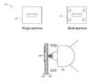
- As utilized herein, the term “aperture” means a surface that does not stop light and refers to describe both a “single aperture” or a “multi-aperture.”
- As utilized herein, the term “front soldered light-emitting diode” means a light-emitting diode that is soldered to the top surface of a printed circuit board, flexible circuit board, or foldable circuit board.
- As utilized herein, the term “back soldered light-emitting diode” means a light-emitting diode that is soldered to the back surface of a printed circuit board, flexible circuit board, or foldable circuit board.
- In some embodiments, the printed circuit board stack may include a layer made by a flexible substrate (flexible circuit component). The flexible circuit component in addition to the receptacle may be used to align light-emitting diodes with the aperture of the printed circuit board. The flexible circuit component may have the light-emitting diodes soldered on it.
- In one embodiment, the entire complex device may be fabricated as a molded interconnected device. The device is created based on a three-dimensional molded (or laser patterned) substrate on which electrical connections and wires are implemented. A fabrication process called “MIPTEC” by Panasonic Corporation may be used to achieve very high precision fabrication of three-dimensional ceramic or resin substrates. Accuracy for fabrication is in the range of tens of micron. Wire bonding and flip-chip mounting of the light emitting diode die may also be used.
- The three-dimensional fabrication provides precise alignment between the apertures and the light emitting diodes in a very compact size (e.g., possible to design a printed circuit board, light-emitting diodes, and aperture assembly with less than one millimeter thickness). The assembly may be made of ceramic material to dissipate the heat from the light-emitting diodes, which may be front-soldered or back-soldered.
- In accordance with embodiments of the invention, the devices may be fabricated to be used as illumination system for the reading of 1D barcodes. The device may have one or more of the following characteristics: illumination pattern with sharp edges, compact size (aperture-LED distance about 0.2 mm, total track less than 10 mm), precise and reliable alignment between the aperture and the other components of the system, high mechanical robustness, and low cost realization.
FIG. 1 illustrates anexemplary aperture 110 and printedcircuit board 120 of a complex device in accordance with embodiments of the invention. In one embodiment, the complex device may be included inside apattern projection system 100 for an aiming system or for providing visual feedback to the user. Thepattern projection system 100 includes the printed circuit board, which is etched or machined with theaperture 110 and alens system 140.- A desired pattern for illuminating, aiming, or providing visual feedback may be projected by the
pattern projection system 100. The shape of the projected pattern depends both on thelenses 140 and on theaperture 110. The light-emitting diodes130 (e.g., front-soldered light-emitting diodes or back-soldered light-emitting diodes) may be soldered to the printedcircuit board 120. - In one embodiment, the light-emitting
diodes 130 are chosen to maintain small compact dimensions and high efficiency in light extraction. In particular, a small emitting area is a key factor for achieving a compact system. Soldering a light-emitting diode on the front surface of the printedcircuit board 120 is a front-soldered light-emitting diode. Alternatively, soldering a light-emitting diode on the back surface of the printedcircuit board 120 is the back-soldered light-emitting diodes. - The
pattern projection system 100 is composed of one or morelight emitting diodes 130, an aperture, and one or more lenses. The assembly of all the parts in one structure guarantees the correct alignment between all the components and provides the needed mechanical robustness. In some embodiments, the aperture is created directly in the printed circuit board during the fabrication processes. Accordingly, the printedcircuit board 120 may be an optical component of thepattern projection system 100. - In some embodiments, the lenses of the
pattern projection system 100 are optimized for reducing the aberrations of the projected pattern, obtaining sharp edges, uniform light intensity and high efficiency. The optical structure may include one or more lenses that are spherical, aspherical or free-form. The lenses may be made from a plastic material or glass. - In some embodiments, a back-soldered light-emitting diode is placed in a receptacle of a printed circuit board. The printed circuit board is fabricated with one or more receptacles and one or more apertures. The receptacles may be shaped to align the light-emitting diodes with the apertures.
FIG. 2 illustrates an exemplary configuration of a light emittingdiode projection system 200 in accordance with embodiments of the invention. The light emittingdiode projection system 200 includes a printedcircuit board 210 having a receptacle and aperture. The light-emittingdiode 220 is place in the receptacle and the light generated by the light-emittingdiode 220 traverses the aperture of the printedcircuit board 210. In one embodiment, the light-emitting diode is a back-soldered light-emitting diode.- In one embodiment, the aperture and receptacle are created directly in the printed
circuit board 210 by exploiting one of the metal layers of the printed circuit board. Both the receptacle and the aperture of the metal layer can be created by shaping the aperture and receptacle during fabrication. Materials used during fabrication include FR4 for the substrate and copper for the metal layers but the embodiments of the invention are not limited to these materials. During fabrication of the light emittingdiode projection system 200, the minimum thickness of the aperture depends on the thickness of the metal layer on which the aperture is fabricated. However, the maximum thickness of the assembly including the light-emitting diode and printed circuit board may be about one millimeter in accordance with embodiments of the invention. - Accordingly, the printed circuit board is configured to provide, among other things, precise alignment between the aperture and the light-emitting diode and a compact light emitting diode projection system200 (i.e., printed-circuit board, light-emitting diode, aperture assembly may have less than one mm thickness).
- In other embodiments, a complex device may include a combination of more than one substrate with spacers for ensuring proper alignment. The substrates include a printed circuit board substrate, receptacle substrate, and aperture substrate. A front-soldered or back-soldered light-emitting diode is placed in a receptacle substrate above the printed circuit board substrate. The aperture substrate is placed above the receptacle substrate. The receptacles of the receptacle substrate may be shaped to align the light-emitting diodes with the apertures.
FIG. 3 illustrates an exemplary buffer zone in thecomplex device 300 in accordance with embodiments of the invention. Thecomplex device 300 may include several substrates (310,320, and330) that are aligned to position the light-emitting diode for a projection system. The substrates include a printedcircuit board layer 310, areceptacle substrate 320, and anaperture substrate 330.- The printed
circuit board substrate 310 may include a light-emitting diode. The light emitting diode is soldered to the printedcircuit board substrate 310. The printedcircuit board substrate 310 may include a plurality of pinholes to receive pins or contacts that align each of the substrates (310,320, and330). - Above the printed
circuit board substrate 310 is areceptacle substrate 320. The receptacle substrate may operate as a spacer between the printedcircuit board substrate 310 and theaperture substrate 330. Thereceptacle substrate 320 may include a receptacle for the light-emitting diode. The receptacle in thereceptacle substrate 320 may be used to align the light-emitting diode with the aperture of theaperture substrate 330. Additionally, thereceptacle substrate 320 may be used to alter a distance between the light-emitting diode and the aperture by increasing or decreasing the size of thereceptacle substrate 320. - In some embodiments, the aperture is created in
aperture substrate 330. Theaperture substrate 330 may consist of a substrate with one or more holes for light to pass through. Theaperture substrate 330 is positioned in front of the light emitting diode that soldered to the printedcircuit board substrate 310. Theaperture substrate 330 is also positioned in front of thereceptacle substrate 320. - In one embodiment, the aperture substrate is at a distance from the printed circuit board defined by the size of the
receptacle substrate 320. Both thereceptacle substrate 320 andaperture substrate 330 may be fabricated from FR4, plastic, or metal materials (but not limited to). The alignment of the substrates (310,320, and330) may be guaranteed by the mechanical structure (e.g., 2 or more pins passing through pinholes in all the layers. Optionally, the pins can be electrically conductive and used as electric contacts to connect the device to a driving circuit. - Accordingly, embodiments of the invention provide a complex device with small and thin apertures that are operable with either front-soldered light-emitting diodes or back-soldered light-emitting diodes.
- In other embodiments, the printed circuit board may include a flexible circuit attachment. Optionally, the flexible circuit attachment may be used to position the light emitting diode in a receptacle of the printed circuit board.
FIG. 4 illustrates an exemplary rigid printedcircuit board 430 andflexible circuit board 410 in accordance with embodiments of the invention. Thecomplex device 400 may include aflexible circuit board 410, light-emittingdiode 420, and printedcircuit board 430.- The
flexible circuit board 410 may be optionally engaged to align thelight emitting diode 420 and with an aperture of the printedcircuit board 430. The flexible circuit board, in some embodiments, is attached to the printedcircuit board 430 along one of the edges. Theflexible circuit board 410 is foldable to position the light-emittingdiode 420 in the receptacle of the printedcircuit board 430. - The printed
circuit board 430 is fabricated with the aperture and receptacle in certain embodiments. The printedcircuit board 430 may include an area for soldering the light-emittingdiode 420. After the light-emitting diode420 (e.g. back-soldered light-emitting diode) is positioned within the receptacle it may be soldered to the printed circuit board. - Accordingly, embodiments of the invention provide a flexible circuit board that may be engaged to align the light-emitting diode in the receptacle of the printed circuit board. The light-emitting diodes are then soldered to the printed circuit board. The light generated by the light-emitting diodes pass through an aperture of the printed circuit board.
- In one embodiment, a complex device may include a foldable circuit board that is fabricated with the aperture. The foldable circuit board may be a substrate that is positioned above the printed circuit board or in between other substrates of the printed circuit board. The foldable circuit board, in certain embodiments, may include wires that are soldered to light-emitting diodes. In some embodiments, the complex device includes the printed circuit board, the foldable circuit board, and one or more light-emitting diodes. The printed circuit board may have one or more receptacles. The foldable circuit member, in turn, is coupled to the printed circuit board. And the foldable circuit board may have at least one aperture. The one or more light-emitting diodes are positioned within the one or more receptacles of the printed circuit board.
FIG. 5 illustrates an exemplaryfoldable circuit board 510 providing self-alignment in accordance with embodiments of the invention. Thecomplex device 500 includes a printed circuit board with afoldable circuit board 510. In one embodiment, thefoldable circuit board 510 is a substrate that is positioned above the printed circuit board or in between other substrates of the printed circuit board. An aperture may be fabricated in thefoldable circuit board 510. And the printed circuit board may include one or more receptacles to receive the one or more light emitting diodes. The one or more light-emitting diodes are aligned with the one or more receptacles via thefoldable circuit board 510.- In one embodiment, the one or more light-emitting diodes are soldered to the
foldable circuit board 510. In other embodiments, the one or more light-emitting diodes are soldered to the printed circuit board. The one or more light-emitting diodes are selected from: front-soldered light emitting diodes or back-soldered light emitting diodes. - Accordingly, the
foldable circuit member 510 provides precise alignment of light-emitting diodes with the aperture of thefoldable circuit board 510 and the receptacle of the printed circuit board. The printed circuit board, foldable circuit board, light-emitting diode assembly may be fabricated in a compact size (e.g., at most one millimeter thickness). - In summary, several configurations for a light-emitting diodes projection system are explained above. The complex devices with light-emitting diode projection system may be scanning device in at least one embodiment. The scanning device includes one or more light-emitting diodes, and a printed circuit board. The printed circuit board is fabricated with one or more apertures and one or more receptacles, in one embodiment. The printed circuit board consists of: a base substrate, a receptacle substrate, and an aperture substrate. The one or more receptacles are positioned behind the aperture and configured to receive the one or more light-emitting diodes. A lens is disposed above the one or more apertures of the printed circuit board, which may be a ceramic material.
- The foregoing descriptions of the embodiments of the invention are illustrative, and modifications in configuration and implementation will occur to persons skilled in the art. Although the subject matter has been described in language specific to structural features or methodological acts, it is to be understood that the subject matter defined in the appended claims is not necessarily limited to the specific features or acts described above. Rather, the specific features and acts described above are disclosed as example forms of implementing the claims. The scope of the invention is accordingly intended to be limited only by the following claims.
Claims (20)
Priority Applications (3)
| Application Number | Priority Date | Filing Date | Title |
|---|---|---|---|
| US14/567,766US10775028B2 (en) | 2014-12-11 | 2014-12-11 | Printed circuit board aperture based illumination system for pattern projection |
| PCT/IB2015/059555WO2016092523A1 (en) | 2014-12-11 | 2015-12-11 | Printed circuit board aperture based illumination system for pattern projection |
| EP15819879.6AEP3231265B1 (en) | 2014-12-11 | 2015-12-11 | Printed circuit board aperture based illumination system for pattern projection |
Applications Claiming Priority (1)
| Application Number | Priority Date | Filing Date | Title |
|---|---|---|---|
| US14/567,766US10775028B2 (en) | 2014-12-11 | 2014-12-11 | Printed circuit board aperture based illumination system for pattern projection |
Publications (2)
| Publication Number | Publication Date |
|---|---|
| US20160169488A1true US20160169488A1 (en) | 2016-06-16 |
| US10775028B2 US10775028B2 (en) | 2020-09-15 |
Family
ID=55069034
Family Applications (1)
| Application Number | Title | Priority Date | Filing Date |
|---|---|---|---|
| US14/567,766ActiveUS10775028B2 (en) | 2014-12-11 | 2014-12-11 | Printed circuit board aperture based illumination system for pattern projection |
Country Status (3)
| Country | Link |
|---|---|
| US (1) | US10775028B2 (en) |
| EP (1) | EP3231265B1 (en) |
| WO (1) | WO2016092523A1 (en) |
Cited By (1)
| Publication number | Priority date | Publication date | Assignee | Title |
|---|---|---|---|---|
| US20220412726A1 (en)* | 2021-06-29 | 2022-12-29 | Beijing Xiaomi Mobile Software Co., Ltd. | Laser emitter, depth camera and electronic device |
Citations (18)
| Publication number | Priority date | Publication date | Assignee | Title |
|---|---|---|---|---|
| US5859418A (en)* | 1996-01-25 | 1999-01-12 | Symbol Technologies, Inc. | CCD-based bar code scanner with optical funnel |
| US20020024808A1 (en)* | 2000-03-14 | 2002-02-28 | Yoshinobu Suehiro | Light source device |
| US20040032728A1 (en)* | 2002-08-19 | 2004-02-19 | Robert Galli | Optical assembly for LED chip package |
| US20040227146A1 (en)* | 2003-05-14 | 2004-11-18 | Jiahn-Chang Wu | Solderless connection in LED module |
| US6999318B2 (en)* | 2003-07-28 | 2006-02-14 | Honeywell International Inc. | Heatsinking electronic devices |
| US7044620B2 (en)* | 2004-04-30 | 2006-05-16 | Guide Corporation | LED assembly with reverse circuit board |
| US20070041190A1 (en)* | 2005-08-17 | 2007-02-22 | Au Optronics Corp. | Bottom lighting module |
| US20080225508A1 (en)* | 2007-03-13 | 2008-09-18 | Lite-On Technology Corporation | Light-emitting device and electronic device using the same |
| US20080285303A1 (en)* | 2006-01-31 | 2008-11-20 | Fujitsu Limited | Optical module and manufacturing method thereof |
| US7556400B2 (en)* | 2006-03-20 | 2009-07-07 | Jiahn-Chang Wu | Backside accessible display |
| US20090297103A1 (en)* | 2008-06-02 | 2009-12-03 | Avago Technologies Fiber Ip (Singapore) Pte. Ltd. | Optical subassembly for an electro-optical assembly |
| US20100182788A1 (en)* | 2009-01-19 | 2010-07-22 | Osram Sylvania Inc. | Led lamp assembly |
| US20110163649A1 (en)* | 2008-06-10 | 2011-07-07 | Swan-Lite Manufacturing Co., Ltd. | Lighting Apparatus |
| US20120201007A1 (en)* | 2011-02-09 | 2012-08-09 | Taiwan Semiconductor Manufacturing Company, Ltd. | Systems and methods providing thermal spreading for an led module |
| US20130027953A1 (en)* | 2011-07-28 | 2013-01-31 | Visteon Global Technologies, Inc | Laser-formed baffle |
| US20140334159A1 (en)* | 2013-05-13 | 2014-11-13 | River Point, Llc | Medical Headlamp Optical Arrangement |
| US20150049484A1 (en)* | 2012-02-16 | 2015-02-19 | Osram Gmbh | Lighting module |
| US20160033713A1 (en)* | 2014-07-29 | 2016-02-04 | Szu-Wei Sun | Backlight Assembly with Brightness Enhancing Arrangement |
Family Cites Families (14)
| Publication number | Priority date | Publication date | Assignee | Title |
|---|---|---|---|---|
| US6384473B1 (en) | 2000-05-16 | 2002-05-07 | Sandia Corporation | Microelectronic device package with an integral window |
| US6949771B2 (en) | 2001-04-25 | 2005-09-27 | Agilent Technologies, Inc. | Light source |
| KR100419611B1 (en) | 2001-05-24 | 2004-02-25 | 삼성전기주식회사 | A Light Emitting Diode, a Lighting Emitting Device Using the Same and a Fabrication Process therefor |
| JP4226796B2 (en) | 2001-05-30 | 2009-02-18 | 株式会社日立製作所 | Liquid crystal display |
| JP4045781B2 (en) | 2001-08-28 | 2008-02-13 | 松下電工株式会社 | Light emitting device |
| JP4303610B2 (en) | 2003-05-19 | 2009-07-29 | 富士フイルム株式会社 | Multilayer wiring board, component mounting method, and imaging apparatus |
| WO2007002644A2 (en) | 2005-06-27 | 2007-01-04 | Lamina Lighting, Inc. | Light emitting diode package and method for making same |
| US8362603B2 (en) | 2006-09-14 | 2013-01-29 | Luminus Devices, Inc. | Flexible circuit light-emitting structures |
| KR100831593B1 (en) | 2007-04-23 | 2008-05-23 | 삼성전기주식회사 | Printed circuit board and manufacturing method thereof, via hole drilling apparatus |
| JP2009117661A (en) | 2007-11-07 | 2009-05-28 | Tokai Rika Co Ltd | Printed circuit board |
| JP5417844B2 (en) | 2008-03-06 | 2014-02-19 | 豊田合成株式会社 | LED lamp device and manufacturing method of LED lamp device |
| US8981629B2 (en) | 2008-08-26 | 2015-03-17 | Albeo Technologies, Inc. | Methods of integrating LED chips with heat sinks, and LED-based lighting assemblies made thereby |
| DE102008047406A1 (en) | 2008-09-09 | 2010-03-11 | Ibl-Hydronic | Film keyboard for control of e.g. vehicle, has printed circuit board connected with another board, so that distance of LED up to film is enlarged, where enlarged surface of film is illuminated at region of display element |
| DE202013011008U1 (en) | 2013-12-16 | 2014-07-18 | Balluff Gmbh | Optical transmitting and receiving unit for an optoelectronic sensor |
- 2014
- 2014-12-11USUS14/567,766patent/US10775028B2/enactiveActive
- 2015
- 2015-12-11EPEP15819879.6Apatent/EP3231265B1/enactiveActive
- 2015-12-11WOPCT/IB2015/059555patent/WO2016092523A1/enactiveApplication Filing
Patent Citations (18)
| Publication number | Priority date | Publication date | Assignee | Title |
|---|---|---|---|---|
| US5859418A (en)* | 1996-01-25 | 1999-01-12 | Symbol Technologies, Inc. | CCD-based bar code scanner with optical funnel |
| US20020024808A1 (en)* | 2000-03-14 | 2002-02-28 | Yoshinobu Suehiro | Light source device |
| US20040032728A1 (en)* | 2002-08-19 | 2004-02-19 | Robert Galli | Optical assembly for LED chip package |
| US20040227146A1 (en)* | 2003-05-14 | 2004-11-18 | Jiahn-Chang Wu | Solderless connection in LED module |
| US6999318B2 (en)* | 2003-07-28 | 2006-02-14 | Honeywell International Inc. | Heatsinking electronic devices |
| US7044620B2 (en)* | 2004-04-30 | 2006-05-16 | Guide Corporation | LED assembly with reverse circuit board |
| US20070041190A1 (en)* | 2005-08-17 | 2007-02-22 | Au Optronics Corp. | Bottom lighting module |
| US20080285303A1 (en)* | 2006-01-31 | 2008-11-20 | Fujitsu Limited | Optical module and manufacturing method thereof |
| US7556400B2 (en)* | 2006-03-20 | 2009-07-07 | Jiahn-Chang Wu | Backside accessible display |
| US20080225508A1 (en)* | 2007-03-13 | 2008-09-18 | Lite-On Technology Corporation | Light-emitting device and electronic device using the same |
| US20090297103A1 (en)* | 2008-06-02 | 2009-12-03 | Avago Technologies Fiber Ip (Singapore) Pte. Ltd. | Optical subassembly for an electro-optical assembly |
| US20110163649A1 (en)* | 2008-06-10 | 2011-07-07 | Swan-Lite Manufacturing Co., Ltd. | Lighting Apparatus |
| US20100182788A1 (en)* | 2009-01-19 | 2010-07-22 | Osram Sylvania Inc. | Led lamp assembly |
| US20120201007A1 (en)* | 2011-02-09 | 2012-08-09 | Taiwan Semiconductor Manufacturing Company, Ltd. | Systems and methods providing thermal spreading for an led module |
| US20130027953A1 (en)* | 2011-07-28 | 2013-01-31 | Visteon Global Technologies, Inc | Laser-formed baffle |
| US20150049484A1 (en)* | 2012-02-16 | 2015-02-19 | Osram Gmbh | Lighting module |
| US20140334159A1 (en)* | 2013-05-13 | 2014-11-13 | River Point, Llc | Medical Headlamp Optical Arrangement |
| US20160033713A1 (en)* | 2014-07-29 | 2016-02-04 | Szu-Wei Sun | Backlight Assembly with Brightness Enhancing Arrangement |
Cited By (1)
| Publication number | Priority date | Publication date | Assignee | Title |
|---|---|---|---|---|
| US20220412726A1 (en)* | 2021-06-29 | 2022-12-29 | Beijing Xiaomi Mobile Software Co., Ltd. | Laser emitter, depth camera and electronic device |
Also Published As
| Publication number | Publication date |
|---|---|
| EP3231265A1 (en) | 2017-10-18 |
| US10775028B2 (en) | 2020-09-15 |
| WO2016092523A1 (en) | 2016-06-16 |
| EP3231265B1 (en) | 2023-08-30 |
Similar Documents
| Publication | Publication Date | Title |
|---|---|---|
| US8128260B2 (en) | Spread lens with refraction parts, and lighting device | |
| US10741993B2 (en) | Laser component and method of producing a laser component | |
| TWI354914B (en) | Method for locating a light source relative to opt | |
| US10495278B2 (en) | Vehicle lighting device with adjustable alignment frame for an optical element and method for assembling a lighting device with an adjustable frame for an optical element | |
| US12230621B2 (en) | Optical navigation module performing lateral detection | |
| CN106885158B (en) | Lighting module and application thereof | |
| CN105737026B (en) | A kind of illumination module of bar code recognizing apparatus | |
| US20160349469A1 (en) | Manufacturing method of printed circuit board, printed circuit board, and optical device | |
| US8840274B1 (en) | Method and apparatus for a protective case including an optical system | |
| CN204190804U (en) | Back case assembly for mobile phone and mobile phone having same | |
| US10775028B2 (en) | Printed circuit board aperture based illumination system for pattern projection | |
| TWI603029B (en) | Light emitting module | |
| CN103926659A (en) | Optical communication module | |
| US8727641B2 (en) | Optical connector | |
| US20140153871A1 (en) | Optical coupling element and optical-electric converting module using same | |
| US9714753B2 (en) | Assembly for emitting light having an LED, a circuit board, and an optical element | |
| CN208239782U (en) | Irradiate mould group and its Multifunctional imaging device | |
| US20140327905A1 (en) | Method for detecting deviation of optial axis of lens and method for positioning lens to light source | |
| US9709243B2 (en) | LED traffic signal light module | |
| US20240255643A1 (en) | Distance measurement camera module | |
| JPS5982779A (en) | Mounting method of optical integrated circuit | |
| KR20190066700A (en) | Lens and light emitting package comprising the same | |
| CN104765107A (en) | Photoelectric conversion module | |
| US20060187980A1 (en) | Thin laser module | |
| US20140212098A1 (en) | Optical connector |
Legal Events
| Date | Code | Title | Description |
|---|---|---|---|
| AS | Assignment | Owner name:DATALOGIC IP TECH S.R.L., ITALY Free format text:ASSIGNMENT OF ASSIGNORS INTEREST;ASSIGNORS:CANINI, FEDERICO;GUAGLIUMI, ANNA;BOTTAZZI, DAVIDE;REEL/FRAME:036962/0295 Effective date:20151104 | |
| STPP | Information on status: patent application and granting procedure in general | Free format text:FINAL REJECTION MAILED | |
| STPP | Information on status: patent application and granting procedure in general | Free format text:DOCKETED NEW CASE - READY FOR EXAMINATION | |
| STPP | Information on status: patent application and granting procedure in general | Free format text:NON FINAL ACTION MAILED | |
| STPP | Information on status: patent application and granting procedure in general | Free format text:RESPONSE TO NON-FINAL OFFICE ACTION ENTERED AND FORWARDED TO EXAMINER | |
| STPP | Information on status: patent application and granting procedure in general | Free format text:FINAL REJECTION MAILED | |
| STPP | Information on status: patent application and granting procedure in general | Free format text:NOTICE OF ALLOWANCE MAILED -- APPLICATION RECEIVED IN OFFICE OF PUBLICATIONS | |
| STPP | Information on status: patent application and granting procedure in general | Free format text:NOTICE OF ALLOWANCE MAILED -- APPLICATION RECEIVED IN OFFICE OF PUBLICATIONS | |
| STPP | Information on status: patent application and granting procedure in general | Free format text:PUBLICATIONS -- ISSUE FEE PAYMENT VERIFIED | |
| STCF | Information on status: patent grant | Free format text:PATENTED CASE | |
| MAFP | Maintenance fee payment | Free format text:PAYMENT OF MAINTENANCE FEE, 4TH YEAR, LARGE ENTITY (ORIGINAL EVENT CODE: M1551); ENTITY STATUS OF PATENT OWNER: LARGE ENTITY Year of fee payment:4 |