US20160165153A1 - Ambient infrared detection in solid state sensors - Google Patents
Ambient infrared detection in solid state sensorsDownload PDFInfo
- Publication number
- US20160165153A1 US20160165153A1US14/993,256US201614993256AUS2016165153A1US 20160165153 A1US20160165153 A1US 20160165153A1US 201614993256 AUS201614993256 AUS 201614993256AUS 2016165153 A1US2016165153 A1US 2016165153A1
- Authority
- US
- United States
- Prior art keywords
- pixels
- image sensor
- sensor device
- region
- image
- Prior art date
- Legal status (The legal status is an assumption and is not a legal conclusion. Google has not performed a legal analysis and makes no representation as to the accuracy of the status listed.)
- Granted
Links
Images


Classifications
- G—PHYSICS
- G03—PHOTOGRAPHY; CINEMATOGRAPHY; ANALOGOUS TECHNIQUES USING WAVES OTHER THAN OPTICAL WAVES; ELECTROGRAPHY; HOLOGRAPHY
- G03B—APPARATUS OR ARRANGEMENTS FOR TAKING PHOTOGRAPHS OR FOR PROJECTING OR VIEWING THEM; APPARATUS OR ARRANGEMENTS EMPLOYING ANALOGOUS TECHNIQUES USING WAVES OTHER THAN OPTICAL WAVES; ACCESSORIES THEREFOR
- G03B13/00—Viewfinders; Focusing aids for cameras; Means for focusing for cameras; Autofocus systems for cameras
- G03B13/02—Viewfinders
- H—ELECTRICITY
- H04—ELECTRIC COMMUNICATION TECHNIQUE
- H04N—PICTORIAL COMMUNICATION, e.g. TELEVISION
- H04N5/00—Details of television systems
- H04N5/30—Transforming light or analogous information into electric information
- H04N5/33—Transforming infrared radiation
- H01L27/14621—
- H01L27/14623—
- H01L27/14625—
- H01L27/14649—
- H—ELECTRICITY
- H04—ELECTRIC COMMUNICATION TECHNIQUE
- H04N—PICTORIAL COMMUNICATION, e.g. TELEVISION
- H04N23/00—Cameras or camera modules comprising electronic image sensors; Control thereof
- H04N23/20—Cameras or camera modules comprising electronic image sensors; Control thereof for generating image signals from infrared radiation only
- H—ELECTRICITY
- H04—ELECTRIC COMMUNICATION TECHNIQUE
- H04N—PICTORIAL COMMUNICATION, e.g. TELEVISION
- H04N25/00—Circuitry of solid-state image sensors [SSIS]; Control thereof
- H04N25/70—SSIS architectures; Circuits associated therewith
- H04N25/76—Addressed sensors, e.g. MOS or CMOS sensors
- H04N5/374—
- H—ELECTRICITY
- H10—SEMICONDUCTOR DEVICES; ELECTRIC SOLID-STATE DEVICES NOT OTHERWISE PROVIDED FOR
- H10F—INORGANIC SEMICONDUCTOR DEVICES SENSITIVE TO INFRARED RADIATION, LIGHT, ELECTROMAGNETIC RADIATION OF SHORTER WAVELENGTH OR CORPUSCULAR RADIATION
- H10F39/00—Integrated devices, or assemblies of multiple devices, comprising at least one element covered by group H10F30/00, e.g. radiation detectors comprising photodiode arrays
- H10F39/10—Integrated devices
- H10F39/12—Image sensors
- H10F39/18—Complementary metal-oxide-semiconductor [CMOS] image sensors; Photodiode array image sensors
- H10F39/184—Infrared image sensors
- H—ELECTRICITY
- H10—SEMICONDUCTOR DEVICES; ELECTRIC SOLID-STATE DEVICES NOT OTHERWISE PROVIDED FOR
- H10F—INORGANIC SEMICONDUCTOR DEVICES SENSITIVE TO INFRARED RADIATION, LIGHT, ELECTROMAGNETIC RADIATION OF SHORTER WAVELENGTH OR CORPUSCULAR RADIATION
- H10F39/00—Integrated devices, or assemblies of multiple devices, comprising at least one element covered by group H10F30/00, e.g. radiation detectors comprising photodiode arrays
- H10F39/80—Constructional details of image sensors
- H10F39/805—Coatings
- H10F39/8053—Colour filters
- H—ELECTRICITY
- H10—SEMICONDUCTOR DEVICES; ELECTRIC SOLID-STATE DEVICES NOT OTHERWISE PROVIDED FOR
- H10F—INORGANIC SEMICONDUCTOR DEVICES SENSITIVE TO INFRARED RADIATION, LIGHT, ELECTROMAGNETIC RADIATION OF SHORTER WAVELENGTH OR CORPUSCULAR RADIATION
- H10F39/00—Integrated devices, or assemblies of multiple devices, comprising at least one element covered by group H10F30/00, e.g. radiation detectors comprising photodiode arrays
- H10F39/80—Constructional details of image sensors
- H10F39/805—Coatings
- H10F39/8057—Optical shielding
- H—ELECTRICITY
- H10—SEMICONDUCTOR DEVICES; ELECTRIC SOLID-STATE DEVICES NOT OTHERWISE PROVIDED FOR
- H10F—INORGANIC SEMICONDUCTOR DEVICES SENSITIVE TO INFRARED RADIATION, LIGHT, ELECTROMAGNETIC RADIATION OF SHORTER WAVELENGTH OR CORPUSCULAR RADIATION
- H10F39/00—Integrated devices, or assemblies of multiple devices, comprising at least one element covered by group H10F30/00, e.g. radiation detectors comprising photodiode arrays
- H10F39/80—Constructional details of image sensors
- H10F39/806—Optical elements or arrangements associated with the image sensors
Definitions
- the present inventionrelates generally to optical devices and in particular the present invention relates to image sensors.
- Image sensorsare used in many different types of electronic devices to capture an image.
- consumer devicessuch as video cameras and digital cameras as well as numerous scientific applications use image sensors to capture an image.
- An image sensoris comprised of photosensitive elements that sense incident illumination and produces an electrical signal indicative of that illumination.
- Each photosensitive elementis typically referred to as a picture element or pixel.
- Image sensorsinclude charge coupled devices (CCD) and complementary metal oxide semiconductor (CMOS) sensors. Imaging sensors may be capable of capturing grayscale and/or color images. Imaging sensors capable of capturing color images often employ a color filter array (CFA) to separate visible illumination of different color. For example, each of the pixels can be covered with a red, green, or blue filter according to a specific pattern. For example, the Bayer pattern has a repeating pattern of an alternating row of green and red and an alternating row of blue and green. As a result of the filtering, each pixel of the color image captured by a CMOS sensor with CFA responds to only the illumination of wavelengths determined by the color filter of the three primary light colors.
- CFAcolor filter array
- CFA color filtersare typically transparent to infrared illumination.
- an infrared-cutoff filteris typically placed in front of the sensor to ensure that only visible wavelength illumination reaches the sensor. This is done to make possible accurate color reproduction in captured images.
- White balanceis the compensation of an image for variation in color temperature of scene illuminant. Images are adjusted in such a way that gray objects will look gray when displayed on a standard output device with a predefined color temperature. Other colors displayed on the output device will also appear as they appeared during image capture. Without white balance, images captured using illuminants having a low temperature will exhibit a reddish cast when displayed on a standard RGB monitor with the color temperature of the white point of 6500 K. Illuminants of higher color temperature can create a bluish cast. The human eye can compensate for the different color temperatures. Both film and digital cameras, however, need to correct for different light sources in order to render an image in its true colors.
- the color correctioncan be accomplished manually by the camera user attaching a color correction filter over the lens.
- a digital cameracan correct the color temperature automatically by estimating the color temperature of the scene illuminant. Then the entire image is adjusted by the difference between the scene illuminant color temperature and the color temperature of the white point of the target output device (e.g., a standard display).
- the white balance algorithmhas to be informed as to the correct color temperature of the scene illuminant.
- the color temperature of the illuminantcan be reliably identified if one knows which objects in the scene are white. Determining the current lighting conditions in a digital camera may be difficult since cameras cannot reliably automatically identify which objects in the scene are white and which are not and thus must rely on other estimation techniques.
- illumination sourcesoften vary with respect to how much infrared radiation they emit. Having an estimate of how much infrared radiation is present in the scene compared to visible illumination can provide information about the nature of the illuminant. For example, incandescent lamps emit visible light accompanied with strong infrared content. Office fluorescent lighting typically emits very little infrared when compared to scene luminance.
- Outdoor daylightcontains moderate amounts of infrared compared to scene luminance.
- FIG. 1shows a cross-sectional view of one embodiment of a portion of an image sensor.
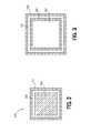
- FIG. 2shows a top view of one embodiment of an image sensor.
- FIG. 3shows a top view of the image sensor that is beneath the infrared filter.
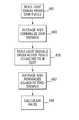
- FIG. 4shows a flowchart of one embodiment of an IR sensing method.
- FIG. 5shows a flowchart of one embodiment for determining IR avg .
- FIG. 6shows a block diagram of one embodiment of an imaging system of the present invention.
- FIG. 7shows a graph of pixel response for the IR-sensitive and IR-shielded pixels of an image sensor.
- FIG. 1illustrates a cross-sectional view of one embodiment of an image sensor. For purposes of clarity, not all of the layers are shown in this figure. For example, there may be metal interconnect layers formed between the layers shown as well as dielectric layers for insulation purposes.
- the sensoris comprised of a substrate 130 that incorporates a plurality of pixels or photodiodes 101 - 104 .
- the photodiodes 101 - 104are responsible for converting light into an electrical signal for use by the circuitry that reads the photodiode information. The higher the intensity of the light that strikes the photodiode 101 - 104 , the greater the charge collected.
- a color filter array (CFA) 112is positioned over the photodiodes 101 - 104 .
- This layercomprises the different color filters required for the color system that is used.
- the filtersmay be red 107 , green 106 , and blue 108 for an additive RGB system or cyan, yellow, magenta, and an extra green for a subtractive CYMG system.
- Each filter colorseparates out that particular color for that photodiode.
- the color filtersare formed in a “Bayer” color filter pattern that is well known in the art.
- An IR cutoff filter 120is positioned over the CFA 112 . This filter blocks IR light from reaching certain ones of the photodiodes 101 - 104 such that only visible light reaches the desired photodiodes 101 - 104 .
- a top view of the embodiments of the IR cutoff filter 120 of the present inventionare illustrated in FIGS. 2 and 3 that are described subsequently.
- a lens 113is positioned over the IR cutoff filter 120 .
- the lens 113is responsible for focusing light on the photodiodes 101 - 104 .
- a plurality of micro-lenses 150can be formed over the photodiodes 101 - 104 .
- Each micro-lens 150can be formed over a corresponding photodiode 101 - 103 .
- Each micro-lens 150focuses the incoming light rays onto its respective photodiode 101 - 104 in order to increase the light gathering efficiency of the photodiode 101 - 104 .
- FIG. 2illustrates a top view of one embodiment of the IR cutoff filter 203 over an image sensor.
- the IR filter 203is deposited directly on the sensor 200 or its protective cover in a patterned fashion.
- the active array pixel filter 203blocks IR from reaching the active pixel array under the filter 203 .
- a slot 205is formed in the periphery of the filter 203 over the array to allow IR to reach the pixels under the slot 205 .
- Optically “black” IR-sensitive (OBIR) pixels 300 as shown in FIG. 3are formed around the periphery of the sensor 200 .
- the OBIR pixels 300are covered with a filter that blocks all visible wavelengths of light from hitting the pixels but is transparent to IR illumination.
- the slot 205 of FIG. 2is only one embodiment of the IR cutoff filter.
- the opening or openings in the IR filtercan be of any shape that can be formed into the filter, thus exposing a predetermined quantity of pixels to IR illumination.
- a slotcan be positioned along only one side of the sensor.
- FIG. 3illustrates the composition of the sensor pixel array lying directly beneath the IR filter.
- This figureshows the regular active array of pixels 301 that is covered by an IR cutoff filter.
- This array 301is surrounded by a ring of OBIR pixels 300 that must be under the opening in the IR filter.
- the OBIR pixels 300are separated from the active pixel array 301 by a ring of barrier pixels 305 .
- the barrier pixels 305shield the active pixel array 301 from IR leaking into periphery active pixels in the active array 301 due to the long wavelength of IR.
- the barrier pixels 305may be shielded from both visible and IR illumination (using a metal layer) and also act to substantially stop any charge leakage from the OBIR pixels 300 into the active pixels 301 . This avoids contaminating the response of active pixels by IR generated charge.
- the OBIR pixels 300are the same type of pixels that are illustrated in FIG. 1 but are not covered by the IR cutoff filter as is the active array of pixels 301 . This allows the OBIR pixels 300 to receive IR illumination.
- FIG. 3also includes optically and IR black (OIRB) pixels 303 that are shielded from all light, both visible and IR. This can be accomplished by a metal layer. These pixels 303 may or may not be under the slot in the IR filter.
- the active pixel array 301is covered with the patterned array of color filters (e.g., Bayer CFA).
- FIG. 4illustrates a flowchart of one embodiment of a method for IR detection in accordance with the image sensors of FIGS. 2 and 3 .
- This methodreads the light signal from the OBIR pixels 401 . These signals are averaged and normalized by analog gain 403 to obtain IR avg as described later with reference to FIG. 5 .
- the light signals from the active pixels adjacent to the IR slot shown in FIG. 3are analyzed 405 . These signals are averaged and normalized 407 by analog gains to generate G avg . G avg is then used to calculate the ratio 409 of G avg /IR avg .
- G avg(avg( P ij green1)/Gain G 1+avg( P ij green2)/Gain G 2)/2 /T int activepixels (1)
- ‘P ij green1’is a light signal from a pixel located in row i and column j in the sensor array, covered by a green CFA filter and located in such rows i that contain pixels covered with green and red CFA filters
- ‘P ij green2’is a light signal from a pixel located in row i and column j in the sensor array, covered by a green CFA filter and located in such rows i that contain pixels covered with green and blue CFA filters
- ‘GainG1’is the gain applied to the green1 pixels
- ‘GainG2’is the gain applied to the green2 pixels
- ‘T int activepixels ’is the integration time the active pixels are receiving.
- GainR, GainB, GainG1, and GainG2 for the Bayer patternare the four typical gains of an image sensor.
- the gainsare applied to corresponding pixels in the Bayer pattern. Since OBIR pixels may only differ from regular pixels by having a black filter, the red, green1, green2, and blue pixel gains keep getting applied to OBIR pixels as well in order to simplify sensor design.
- the light signals from the active pixels adjacent to the IR slot shown in FIG. 3are analyzed 405 . These signals are then averaged and normalized 407 by analog gain to generate G avg .
- IR avgis discussed subsequently with reference to FIG. 5 .
- IR avgis then used to calculate the ratio 409 of G avg /IR avg . Alternate embodiments can calculate other ratios such as Y avg /IR avg where Y avg is the average luminance of pixels after demosaicing and, optionally, color correction.
- FIG. 5illustrates a flowchart of one embodiment for determining IR avg .
- the methodbegins with zeroing a row counter, r 501 .
- the signals from the OBIR pixelsare then read 503 . These signals are used to determine four averages of P ij from the OBIR pixels and are affected by Blue/Red/Green1/Green2 gain. These averages are denoted as IR avgR , IR avgB , IR avgG .
- IR avgG ( r )avg(avg( P ij green1)/Gain G 1, avg( P ij green2)/(Gain G 2)/ T int IR (2)
- IR avgR ( r )avg( P ij red)/Gain R/T int IR (3)
- IR avgB ( r )avg( P ij blue)/Gain B/T int IR (4)
- T int IRis the integration time OBIR and OIRB pixels are receiving, which is typically equal to T int active pixels. If pixel ring r contains no pixels of type green1 or green2, the corresponding term is excluded from the calculation of the average in (2).
- T sata saturation threshold 507 .
- Charge leakageis the result of the fact that infrared photons are absorbed at a higher depth than the visual wavelength photons due to solid state sensor construction typically having a longer average travel distance before the infrared photo-generated carriers are collected.
- the infrared-generated carrierscan leak under the optical shield of the OIRB pixels.
- the OIRB pixelscollect the infrared-generated charge and their response is increased. Illumination free of infrared will have no effect on OIRB pixel response. The magnitude of that component can then be determined in comparison to the visible light illumination of the edge pixels.
- OIRB pixelsare particularly effective in cases where levels of IR radiation are so high as to saturate responses of OBIR pixels.
- the exposure for active pixelsis typically selected to result in capture of visually pleasing images. Since OBIR pixels differ from active pixels only by having a different CFA filter, their exposure would typically be identical to that of the active pixels. This is true unless, optionally, the sensor is specifically designed to allow setting exposure of OBIR pixels independently from active pixels. In such an embodiment, the sensor would require a more complicated design.
- OBIR pixel responsecan be saturated if the scene illuminant has a high IR content. In such case, values of OIRB pixels should be read out instead of OBIR.
- T intIRT intactivepixels
- K iran IR sensitivity coefficient
- IR avg ( r )avg( IR avgR ( r ), IR avgB ( r ), IR avgG ( r ))/Kir( r ) (5)
- IR avgR , IR avgG , and/or IR avgBare less than T sat , or pixels of a certain type (e.g., affected by the blue or red gains) do not exist in ring r, these averages are excluded from the average.
- K ir for inner OIRB pixelsis typically substantially less than 1.
- the coefficientwould get progressively smaller due to reduced sensitivity of inner OIRB pixels.
- K ir (r)can be determined using a calibration procedure.
- the embodiment of the sensor of FIGS. 2 and 3is optimized for use during manufacture of a sensor array.
- the opening in the IR cutoff filtercan be added when the IR filter is formed over the sensor array.
- the IR detection embodimentscan also be used when a sensor array already has an IR cutoff filter covering the entire array of pixels.
- Such an IR detection embodimentrelies on the fact that spectral transmittance of reflective IR-cutoff filters is highly angle dependent. Such filters allow a small amount of IR illumination through when illuminated at an angle other than perpendicular to the filter plane.
- IR sensing in using a visible light sensoris that the level of IR can substantially differ from the level of visible illumination, sometimes by many orders of magnitude.
- OIRB pixelsthe IR is sensed in a high-dynamic-range fashion.
- the present embodimentsrequire only a few changes to the sensor such as forming a black filter over some pixels, a metal layer over other pixels, and forming “barrier” pixels.
- IR sensingthere are also alternative embodiments for IR sensing.
- the exposure of IR pixelscan be controlled independently from active pixels.
- the exposureis varied to avoid overexposure of IR pixels and the OIRB pixels are optional.
- the method for IR sensingis similar to the embodiment of FIGS. 2-5 but not all of the OIRB pixels are shielded completely.
- the pixels adjacent to the OIRB pixelshave a certain area (e.g., 50%) covered by metal.
- the next inner rowis covered by metal to a greater extent (e.g., 75%) and the next row is covered to an even greater amount (e.g., 100%).
- the OIRB pixelsare not used.
- special high dynamic range pixelsare used to sense IR.
- FIG. 6illustrates a block diagram of one embodiment of an imaging system of the present invention.
- the systemcomprises an image sensor 600 as described previously, coupled to a control circuit 601 .
- This systemcan represent a camera or some other imaging device.
- control circuit 601is a processor, microprocessor, or other controller circuitry that reads and processes the image from the image sensor device 600 .
- the imaging systemcan be a digital camera in which the image sensor device 600 is exposed to an image for recording.
- the control circuitry 601executes the above-described embodiments and reads the accumulated charges from the photodiodes of the image sensor device 600 .
- the control circuitry 601may then process this data into an image or simply store the data.
- the data from the systemcan be output to other systems over an I/O circuit 603 .
- the I/O circuit 603may be a Universal Serial Bus (USB) or some other type of bus that can connect the imaging system to a computer or other system.
- USBUniversal Serial Bus
- the embodiments discussed hereinprovide a way to measure the amount of infrared illumination that reaches an image sensor. Knowing the amount of infrared illumination is useful in automatic white balance algorithms.
- a large amount of infrared illuminationinforms the white balance algorithm that the scene is illuminated by an incandescent light source. The white balance algorithm can then shift the color temperature of the received image to adjust for the extra red color cast.
- a low amount of infraredinforms the white balance algorithm that the camera is imaging a scene illuminated by a fluorescent light source, such as office lighting, and the color temperature of the received image must be shifted to remove a greenish cast.
- a moderate amount of infraredindicates that the camera is used outdoors in daylight conditions. In this condition, the white balance would typically remove a blue color cast from the image, if any.
Landscapes
- Engineering & Computer Science (AREA)
- Multimedia (AREA)
- Signal Processing (AREA)
- Physics & Mathematics (AREA)
- General Physics & Mathematics (AREA)
- Color Television Image Signal Generators (AREA)
- Solid State Image Pick-Up Elements (AREA)
Abstract
Description
- This application is a continuation of U.S. application Ser. No. 14/063,069, filed Oct. 25, 2013 (allowed), which is a continuation of U.S. application Ser. No. 12/813,705, filed Jun. 11, 2010 and issued as U.S. Pat. No. 8,569,681 on Oct. 29, 2013, which is a divisional application of application Ser. No. 11/513,582, filed Aug. 31, 2006 and issued as U.S. Pat. No. 7,737,394 on Jun. 15, 2010, which applications are assigned to the assignee of the present invention and the entire contents of which are incorporated herein by reference.
- The present invention relates generally to optical devices and in particular the present invention relates to image sensors.
- Image sensors are used in many different types of electronic devices to capture an image. For example, consumer devices such as video cameras and digital cameras as well as numerous scientific applications use image sensors to capture an image. An image sensor is comprised of photosensitive elements that sense incident illumination and produces an electrical signal indicative of that illumination. Each photosensitive element is typically referred to as a picture element or pixel.
- Image sensors include charge coupled devices (CCD) and complementary metal oxide semiconductor (CMOS) sensors. Imaging sensors may be capable of capturing grayscale and/or color images. Imaging sensors capable of capturing color images often employ a color filter array (CFA) to separate visible illumination of different color. For example, each of the pixels can be covered with a red, green, or blue filter according to a specific pattern. For example, the Bayer pattern has a repeating pattern of an alternating row of green and red and an alternating row of blue and green. As a result of the filtering, each pixel of the color image captured by a CMOS sensor with CFA responds to only the illumination of wavelengths determined by the color filter of the three primary light colors.
- CFA color filters are typically transparent to infrared illumination. In video and still digital cameras, an infrared-cutoff filter is typically placed in front of the sensor to ensure that only visible wavelength illumination reaches the sensor. This is done to make possible accurate color reproduction in captured images.
- White balance is the compensation of an image for variation in color temperature of scene illuminant. Images are adjusted in such a way that gray objects will look gray when displayed on a standard output device with a predefined color temperature. Other colors displayed on the output device will also appear as they appeared during image capture. Without white balance, images captured using illuminants having a low temperature will exhibit a reddish cast when displayed on a standard RGB monitor with the color temperature of the white point of 6500 K. Illuminants of higher color temperature can create a bluish cast. The human eye can compensate for the different color temperatures. Both film and digital cameras, however, need to correct for different light sources in order to render an image in its true colors.
- In a film camera, the color correction can be accomplished manually by the camera user attaching a color correction filter over the lens. A digital camera can correct the color temperature automatically by estimating the color temperature of the scene illuminant. Then the entire image is adjusted by the difference between the scene illuminant color temperature and the color temperature of the white point of the target output device (e.g., a standard display). One problem with this approach is that the white balance algorithm has to be informed as to the correct color temperature of the scene illuminant.
- Various techniques exist in the art to determine the color temperature and spectral content of the illuminant. The color temperature of the illuminant can be reliably identified if one knows which objects in the scene are white. Determining the current lighting conditions in a digital camera may be difficult since cameras cannot reliably automatically identify which objects in the scene are white and which are not and thus must rely on other estimation techniques. However, illumination sources often vary with respect to how much infrared radiation they emit. Having an estimate of how much infrared radiation is present in the scene compared to visible illumination can provide information about the nature of the illuminant. For example, incandescent lamps emit visible light accompanied with strong infrared content. Office fluorescent lighting typically emits very little infrared when compared to scene luminance. Outdoor daylight contains moderate amounts of infrared compared to scene luminance. For the reasons stated above, and for other reasons stated below which will become apparent to those skilled in the art upon reading and understanding the present specification, there is a need in the art for detecting ambient infrared in a sensor equipped with an IR cut-off filter.
FIG. 1 shows a cross-sectional view of one embodiment of a portion of an image sensor.FIG. 2 shows a top view of one embodiment of an image sensor.FIG. 3 shows a top view of the image sensor that is beneath the infrared filter.FIG. 4 shows a flowchart of one embodiment of an IR sensing method.FIG. 5 shows a flowchart of one embodiment for determining IRavg.FIG. 6 shows a block diagram of one embodiment of an imaging system of the present invention.FIG. 7 shows a graph of pixel response for the IR-sensitive and IR-shielded pixels of an image sensor.- In the following detailed description of the invention, reference is made to the accompanying drawings that form a part hereof and in which is shown, by way of illustration, specific embodiments in which the invention may be practiced. In the drawings, like numerals describe substantially similar components throughout the several views. These embodiments are described in sufficient detail to enable those skilled in the art to practice the invention. Other embodiments may be utilized and structural, logical, and electrical changes may be made without departing from the scope of the present invention. The following detailed description is, therefore, not to be taken in a limiting sense, and the scope of the present invention is defined only by the appended claims and equivalents thereof.
FIG. 1 illustrates a cross-sectional view of one embodiment of an image sensor. For purposes of clarity, not all of the layers are shown in this figure. For example, there may be metal interconnect layers formed between the layers shown as well as dielectric layers for insulation purposes.- The sensor is comprised of a
substrate 130 that incorporates a plurality of pixels or photodiodes101-104. The photodiodes101-104 are responsible for converting light into an electrical signal for use by the circuitry that reads the photodiode information. The higher the intensity of the light that strikes the photodiode101-104, the greater the charge collected. - Optionally, a color filter array (CFA)112 is positioned over the photodiodes101-104. This layer comprises the different color filters required for the color system that is used. For example, the filters may be red107, green106, and blue108 for an additive RGB system or cyan, yellow, magenta, and an extra green for a subtractive CYMG system. Each filter color separates out that particular color for that photodiode. In one embodiment, the color filters are formed in a “Bayer” color filter pattern that is well known in the art.
- An
IR cutoff filter 120 is positioned over theCFA 112. This filter blocks IR light from reaching certain ones of the photodiodes101-104 such that only visible light reaches the desired photodiodes101-104. A top view of the embodiments of theIR cutoff filter 120 of the present invention are illustrated inFIGS. 2 and 3 that are described subsequently. - A
lens 113 is positioned over theIR cutoff filter 120. Thelens 113 is responsible for focusing light on the photodiodes101-104. - Optionally, a plurality of
micro-lenses 150 can be formed over the photodiodes101-104. Each micro-lens150 can be formed over a corresponding photodiode101-103. Each micro-lens150 focuses the incoming light rays onto its respective photodiode101-104 in order to increase the light gathering efficiency of the photodiode101-104. FIG. 2 illustrates a top view of one embodiment of theIR cutoff filter 203 over an image sensor. In this embodiment, theIR filter 203 is deposited directly on thesensor 200 or its protective cover in a patterned fashion. The activearray pixel filter 203 blocks IR from reaching the active pixel array under thefilter 203. Aslot 205 is formed in the periphery of thefilter 203 over the array to allow IR to reach the pixels under theslot 205. Optically “black” IR-sensitive (OBIR)pixels 300 as shown inFIG. 3 are formed around the periphery of thesensor 200. TheOBIR pixels 300 are covered with a filter that blocks all visible wavelengths of light from hitting the pixels but is transparent to IR illumination.- The
slot 205 ofFIG. 2 is only one embodiment of the IR cutoff filter. The opening or openings in the IR filter can be of any shape that can be formed into the filter, thus exposing a predetermined quantity of pixels to IR illumination. For example, a slot can be positioned along only one side of the sensor. FIG. 3 illustrates the composition of the sensor pixel array lying directly beneath the IR filter. This figure shows the regular active array ofpixels 301 that is covered by an IR cutoff filter. Thisarray 301 is surrounded by a ring ofOBIR pixels 300 that must be under the opening in the IR filter. TheOBIR pixels 300 are separated from theactive pixel array 301 by a ring ofbarrier pixels 305. Thebarrier pixels 305 shield theactive pixel array 301 from IR leaking into periphery active pixels in theactive array 301 due to the long wavelength of IR. Thebarrier pixels 305 may be shielded from both visible and IR illumination (using a metal layer) and also act to substantially stop any charge leakage from theOBIR pixels 300 into theactive pixels 301. This avoids contaminating the response of active pixels by IR generated charge.- The
OBIR pixels 300 are the same type of pixels that are illustrated inFIG. 1 but are not covered by the IR cutoff filter as is the active array ofpixels 301. This allows theOBIR pixels 300 to receive IR illumination. FIG. 3 also includes optically and IR black (OIRB)pixels 303 that are shielded from all light, both visible and IR. This can be accomplished by a metal layer. Thesepixels 303 may or may not be under the slot in the IR filter. Theactive pixel array 301 is covered with the patterned array of color filters (e.g., Bayer CFA).FIG. 4 illustrates a flowchart of one embodiment of a method for IR detection in accordance with the image sensors ofFIGS. 2 and 3 . This method reads the light signal from theOBIR pixels 401. These signals are averaged and normalized byanalog gain 403 to obtain IRavgas described later with reference toFIG. 5 .- After the averaging and normalization of the OBIR signals403, the light signals from the active pixels adjacent to the IR slot shown in
FIG. 3 are analyzed405. These signals are averaged and normalized407 by analog gains to generate Gavg. Gavgis then used to calculate theratio 409 of Gavg/IRavg. - Averaging the signals is accomplished by the equation:
Gavg=(avg(Pijgreen1)/GainG1+avg(Pijgreen2)/GainG2)/2/Tint activepixels (1)- where ‘Pijgreen1’ is a light signal from a pixel located in row i and column j in the sensor array, covered by a green CFA filter and located in such rows i that contain pixels covered with green and red CFA filters, ‘Pijgreen2’ is a light signal from a pixel located in row i and column j in the sensor array, covered by a green CFA filter and located in such rows i that contain pixels covered with green and blue CFA filters, ‘GainG1’ is the gain applied to the green1 pixels, ‘GainG2’ is the gain applied to the green2 pixels, and ‘Tint activepixels’ is the integration time the active pixels are receiving.
- During a normalization process, GainR, GainB, GainG1, and GainG2 for the Bayer pattern are the four typical gains of an image sensor. The gains are applied to corresponding pixels in the Bayer pattern. Since OBIR pixels may only differ from regular pixels by having a black filter, the red, green1, green2, and blue pixel gains keep getting applied to OBIR pixels as well in order to simplify sensor design.
- Referring again to
FIG. 4 , after the averaging and normalizing of the OBIR signals403, the light signals from the active pixels adjacent to the IR slot shown inFIG. 3 are analyzed405. These signals are then averaged and normalized407 by analog gain to generate Gavg. IRavgis discussed subsequently with reference toFIG. 5 . IRavgis then used to calculate theratio 409 of Gavg/IRavg. Alternate embodiments can calculate other ratios such as Yavg/IRavgwhere Yavgis the average luminance of pixels after demosaicing and, optionally, color correction. FIG. 5 illustrates a flowchart of one embodiment for determining IRavg. The method begins with zeroing a row counter,r 501. The signals from the OBIR pixels are then read503. These signals are used to determine four averages of Pijfrom the OBIR pixels and are affected by Blue/Red/Green1/Green2 gain. These averages are denoted as IRavgR, IRavgB, IRavgG.
IRavgG(r)=avg(avg(Pijgreen1)/GainG1, avg(Pijgreen2)/(GainG2)/Tint IR (2)
IRavgR(r)=avg(Pijred)/GainR/Tint IR (3)
IRavgB(r)=avg(Pijblue)/GainB/Tint IR (4)- where Pijare OBIR pixels from the rthinner pixel ring as detailed below. Tint IRis the integration time OBIR and OIRB pixels are receiving, which is typically equal to Tintactive pixels. If pixel ring r contains no pixels of type green1 or green2, the corresponding term is excluded from the calculation of the average in (2).
- These averages are compared to a
saturation threshold 507, Tsat. This threshold is determined by the maximum pixel value Dmaxthat can be read multiplied by a saturation constant, Ksat(i.e., Tsat=Ksat*Dmax). For example, a maximum pixel value of 1023 multiplied by a constant of 18%. If ring r contains no pixels affected by the blue or red gains, the comparison for the average value of that type of pixel is not performed. - If none of the averages are less than
T sat507, the pixels being considered are all close to IR saturation. Therefore, “more inner” OIRB pixels that are further from the OBIR pixels are then read509. The “more inner” OIRB pixels are read by incrementing therow counter 511 and repeating the OBIR pixel read503. This is repeated until non-saturated pixels are found. Since these pixels are shielded from visible and IR illumination, the signal generated by these pixels is due largely to charge and light leakage from adjacent OBIR pixels, seeFIG. 7 . Hence such signal may be substantially attenuated compared to OBIR pixel response thus allowing to assess IR illumination even when OBIR pixels are overexposed. - Charge leakage is the result of the fact that infrared photons are absorbed at a higher depth than the visual wavelength photons due to solid state sensor construction typically having a longer average travel distance before the infrared photo-generated carriers are collected. Thus, the infrared-generated carriers can leak under the optical shield of the OIRB pixels. The OIRB pixels collect the infrared-generated charge and their response is increased. Illumination free of infrared will have no effect on OIRB pixel response. The magnitude of that component can then be determined in comparison to the visible light illumination of the edge pixels.
- OIRB pixels are particularly effective in cases where levels of IR radiation are so high as to saturate responses of OBIR pixels. For example, as the image sensor operates, the exposure for active pixels is typically selected to result in capture of visually pleasing images. Since OBIR pixels differ from active pixels only by having a different CFA filter, their exposure would typically be identical to that of the active pixels. This is true unless, optionally, the sensor is specifically designed to allow setting exposure of OBIR pixels independently from active pixels. In such an embodiment, the sensor would require a more complicated design.
- When active pixels are exposed in a way optimal for image capture, OBIR pixel response can be saturated if the scene illuminant has a high IR content. In such case, values of OIRB pixels should be read out instead of OBIR.
- After non-saturated pixels are found, the average of the averages that are less than the saturation threshold Tsatis determined513. This is determined by the following equation where, typically, TintIR=Tintactivepixelsand Kiris an IR sensitivity coefficient:
IRavg(r)=avg(IRavgR(r),IRavgB(r),IRavgG(r))/Kir(r) (5)- In the formula above, if IRavgR, IRavgG, and/or IRavgBare less than Tsat, or pixels of a certain type (e.g., affected by the blue or red gains) do not exist in ring r, these averages are excluded from the average.
- If IR coefficient is set to 1 for OBIR, Kir(0) is defined as 1 for OBIR pixels, Kir(0)=1. Kirfor inner OIRB pixels is typically substantially less than 1. For example, the inner row of OIRB pixels could have Kir(1)=0.05. The next row, Kir(2) might have Kir(2)=0.0025. The coefficient would get progressively smaller due to reduced sensitivity of inner OIRB pixels. Kir(r) can be determined using a calibration procedure.
- One such calibration procedure illuminates the sensor with IR that has spectra expected to be encountered in actual operation. A flat field is then imaged. The sensor exposure and gains are adjusted to make responses of OIRB pixels equal to a constant (e.g., Tsat). Exposure Tint(r) is recorded for r=0, as Tint(0). Gains are then frozen. For each inner ring of OIRB pixels, exposure is adjusted to make their responses equal to Tsat. The OIRB pixels probably saturate in this condition. Tint(r) is recorded for r=1, 2, etc. If Kir(0)=1, Kir(r)=Tint(0)/Tint(r).
- The embodiment of the sensor of
FIGS. 2 and 3 is optimized for use during manufacture of a sensor array. The opening in the IR cutoff filter can be added when the IR filter is formed over the sensor array. - The IR detection embodiments can also be used when a sensor array already has an IR cutoff filter covering the entire array of pixels. Such an IR detection embodiment relies on the fact that spectral transmittance of reflective IR-cutoff filters is highly angle dependent. Such filters allow a small amount of IR illumination through when illuminated at an angle other than perpendicular to the filter plane.
- One problem solved by the present embodiments in IR sensing in using a visible light sensor is that the level of IR can substantially differ from the level of visible illumination, sometimes by many orders of magnitude. By using OBIR and OIRB pixels the IR is sensed in a high-dynamic-range fashion. The present embodiments require only a few changes to the sensor such as forming a black filter over some pixels, a metal layer over other pixels, and forming “barrier” pixels.
- There are also alternative embodiments for IR sensing. For example, the exposure of IR pixels can be controlled independently from active pixels. In this embodiment, the exposure is varied to avoid overexposure of IR pixels and the OIRB pixels are optional.
- In yet another embodiment, the method for IR sensing is similar to the embodiment of
FIGS. 2-5 but not all of the OIRB pixels are shielded completely. The pixels adjacent to the OIRB pixels have a certain area (e.g., 50%) covered by metal. The next inner row is covered by metal to a greater extent (e.g., 75%) and the next row is covered to an even greater amount (e.g., 100%). - In still another embodiment, the OIRB pixels are not used. In this embodiment, special high dynamic range pixels are used to sense IR.
FIG. 6 illustrates a block diagram of one embodiment of an imaging system of the present invention. The system comprises animage sensor 600 as described previously, coupled to acontrol circuit 601. This system can represent a camera or some other imaging device.- In one embodiment, the
control circuit 601 is a processor, microprocessor, or other controller circuitry that reads and processes the image from theimage sensor device 600. For example, the imaging system can be a digital camera in which theimage sensor device 600 is exposed to an image for recording. Thecontrol circuitry 601 executes the above-described embodiments and reads the accumulated charges from the photodiodes of theimage sensor device 600. Thecontrol circuitry 601 may then process this data into an image or simply store the data. - The data from the system can be output to other systems over an I/
O circuit 603. The I/O circuit 603 may be a Universal Serial Bus (USB) or some other type of bus that can connect the imaging system to a computer or other system. - In summary, the embodiments discussed herein provide a way to measure the amount of infrared illumination that reaches an image sensor. Knowing the amount of infrared illumination is useful in automatic white balance algorithms. A large amount of infrared illumination informs the white balance algorithm that the scene is illuminated by an incandescent light source. The white balance algorithm can then shift the color temperature of the received image to adjust for the extra red color cast. A low amount of infrared informs the white balance algorithm that the camera is imaging a scene illuminated by a fluorescent light source, such as office lighting, and the color temperature of the received image must be shifted to remove a greenish cast. A moderate amount of infrared indicates that the camera is used outdoors in daylight conditions. In this condition, the white balance would typically remove a blue color cast from the image, if any.
- Although specific embodiments have been illustrated and described herein, it will be appreciated by those of ordinary skill in the art that any arrangement that is calculated to achieve the same purpose may be substituted for the specific embodiments shown. Many adaptations of the invention will be apparent to those of ordinary skill in the art. Accordingly, this application is intended to cover any adaptations or variations of the invention. It is manifestly intended that this invention be limited only by the following claims and equivalents thereof.
Claims (20)
Priority Applications (1)
| Application Number | Priority Date | Filing Date | Title |
|---|---|---|---|
| US14/993,256US10084974B2 (en) | 2006-08-31 | 2016-01-12 | Ambient infrared detection in solid state sensors |
Applications Claiming Priority (4)
| Application Number | Priority Date | Filing Date | Title |
|---|---|---|---|
| US11/513,582US7737394B2 (en) | 2006-08-31 | 2006-08-31 | Ambient infrared detection in solid state sensors |
| US12/813,705US8569681B2 (en) | 2006-08-31 | 2010-06-11 | Ambient infrared detection in solid state sensors |
| US14/063,069US9252176B2 (en) | 2006-08-31 | 2013-10-25 | Ambient infrared detection in solid state sensors |
| US14/993,256US10084974B2 (en) | 2006-08-31 | 2016-01-12 | Ambient infrared detection in solid state sensors |
Related Parent Applications (1)
| Application Number | Title | Priority Date | Filing Date |
|---|---|---|---|
| US14/063,069ContinuationUS9252176B2 (en) | 2006-08-31 | 2013-10-25 | Ambient infrared detection in solid state sensors |
Publications (2)
| Publication Number | Publication Date |
|---|---|
| US20160165153A1true US20160165153A1 (en) | 2016-06-09 |
| US10084974B2 US10084974B2 (en) | 2018-09-25 |
Family
ID=39151673
Family Applications (4)
| Application Number | Title | Priority Date | Filing Date |
|---|---|---|---|
| US11/513,582Active2028-12-07US7737394B2 (en) | 2006-08-31 | 2006-08-31 | Ambient infrared detection in solid state sensors |
| US12/813,705Active2028-11-18US8569681B2 (en) | 2006-08-31 | 2010-06-11 | Ambient infrared detection in solid state sensors |
| US14/063,069Active2027-05-29US9252176B2 (en) | 2006-08-31 | 2013-10-25 | Ambient infrared detection in solid state sensors |
| US14/993,256Active2027-02-16US10084974B2 (en) | 2006-08-31 | 2016-01-12 | Ambient infrared detection in solid state sensors |
Family Applications Before (3)
| Application Number | Title | Priority Date | Filing Date |
|---|---|---|---|
| US11/513,582Active2028-12-07US7737394B2 (en) | 2006-08-31 | 2006-08-31 | Ambient infrared detection in solid state sensors |
| US12/813,705Active2028-11-18US8569681B2 (en) | 2006-08-31 | 2010-06-11 | Ambient infrared detection in solid state sensors |
| US14/063,069Active2027-05-29US9252176B2 (en) | 2006-08-31 | 2013-10-25 | Ambient infrared detection in solid state sensors |
Country Status (1)
| Country | Link |
|---|---|
| US (4) | US7737394B2 (en) |
Families Citing this family (43)
| Publication number | Priority date | Publication date | Assignee | Title |
|---|---|---|---|---|
| US8587562B2 (en)* | 2002-11-04 | 2013-11-19 | Neonode Inc. | Light-based touch screen using elliptical and parabolic reflectors |
| WO2007043036A1 (en) | 2005-10-11 | 2007-04-19 | Prime Sense Ltd. | Method and system for object reconstruction |
| US9330324B2 (en) | 2005-10-11 | 2016-05-03 | Apple Inc. | Error compensation in three-dimensional mapping |
| KR101331543B1 (en) | 2006-03-14 | 2013-11-20 | 프라임센스 엘티디. | Three-dimensional sensing using speckle patterns |
| US7965444B2 (en)* | 2006-08-31 | 2011-06-21 | Micron Technology, Inc. | Method and apparatus to improve filter characteristics of optical filters |
| US8494252B2 (en) | 2007-06-19 | 2013-07-23 | Primesense Ltd. | Depth mapping using optical elements having non-uniform focal characteristics |
| US8462207B2 (en) | 2009-02-12 | 2013-06-11 | Primesense Ltd. | Depth ranging with Moiré patterns |
| US8786682B2 (en) | 2009-03-05 | 2014-07-22 | Primesense Ltd. | Reference image techniques for three-dimensional sensing |
| US8726324B2 (en)* | 2009-03-27 | 2014-05-13 | Motorola Mobility Llc | Method for identifying image capture opportunities using a selected expert photo agent |
| JP2011029810A (en)* | 2009-07-23 | 2011-02-10 | Sony Ericsson Mobile Communications Ab | Imaging device, imaging method, imaging control program, and portable terminal device |
| WO2011013079A1 (en) | 2009-07-30 | 2011-02-03 | Primesense Ltd. | Depth mapping based on pattern matching and stereoscopic information |
| US8830227B2 (en) | 2009-12-06 | 2014-09-09 | Primesense Ltd. | Depth-based gain control |
| US8982182B2 (en) | 2010-03-01 | 2015-03-17 | Apple Inc. | Non-uniform spatial resource allocation for depth mapping |
| WO2012020380A1 (en) | 2010-08-11 | 2012-02-16 | Primesense Ltd. | Scanning projectors and image capture modules for 3d mapping |
| EP2643659B1 (en) | 2010-11-19 | 2019-12-25 | Apple Inc. | Depth mapping using time-coded illumination |
| GB2485996A (en)* | 2010-11-30 | 2012-06-06 | St Microelectronics Res & Dev | A combined proximity and ambient light sensor |
| GB2486000A (en) | 2010-11-30 | 2012-06-06 | St Microelectronics Res & Dev | Optical proximity detectors with arrangements for reducing internal light propagation from emitter to detector |
| US9167138B2 (en) | 2010-12-06 | 2015-10-20 | Apple Inc. | Pattern projection and imaging using lens arrays |
| JP5541137B2 (en)* | 2010-12-15 | 2014-07-09 | ソニー株式会社 | Imaging device, electronic device, solar battery, and manufacturing method of imaging device |
| CA2769358C (en)* | 2011-03-08 | 2016-06-07 | Research In Motion Limited | Quantum dot image sensor with dummy pixels used for intensity calculations |
| JP2014514736A (en)* | 2011-03-16 | 2014-06-19 | ケーエルエー−テンカー コーポレイション | EUV Actinic Reticle Inspection System Using Image Sensor with Thin Film Spectral Purity Filter Coating |
| US9030528B2 (en) | 2011-04-04 | 2015-05-12 | Apple Inc. | Multi-zone imaging sensor and lens array |
| JP2013143520A (en)* | 2012-01-12 | 2013-07-22 | Sony Corp | Image pickup unit and method of manufacturing image pickup unit |
| CN104160240B (en) | 2012-02-15 | 2017-02-22 | 苹果公司 | Scanning depth engine |
| US9158113B2 (en)* | 2012-03-14 | 2015-10-13 | Google Inc. | Integrated display and photosensor |
| DE102012021736B4 (en) | 2012-03-22 | 2021-08-05 | Volkswagen Aktiengesellschaft | Image sensor for visible and infrared light and camera system |
| US8872093B2 (en)* | 2012-04-18 | 2014-10-28 | Apple Inc. | Calibrated image-sensor-based ambient light sensor |
| US9437171B2 (en)* | 2012-12-05 | 2016-09-06 | Texas Instruments Incorporated | Local tone mapping for high dynamic range images |
| US8981512B1 (en)* | 2013-09-18 | 2015-03-17 | Omnivision Technologies, Inc. | Optical shield in a pixel cell planarization layer for black level correction |
| KR102071325B1 (en)* | 2013-09-27 | 2020-04-02 | 매그나칩 반도체 유한회사 | Optical sensor sensing illuminance and proximity |
| JP6429176B2 (en)* | 2014-09-16 | 2018-11-28 | 華為技術有限公司Huawei Technologies Co.,Ltd. | Image processing method and apparatus |
| KR102310586B1 (en)* | 2015-04-21 | 2021-10-13 | 에스케이하이닉스 주식회사 | 4-color pixel image sensor with decrease of ir pixel for near ir |
| US9972651B2 (en)* | 2015-08-03 | 2018-05-15 | Visera Technologies Company Limited | Spectrum-inspection device |
| US10412280B2 (en) | 2016-02-10 | 2019-09-10 | Microsoft Technology Licensing, Llc | Camera with light valve over sensor array |
| US10156665B2 (en)* | 2016-06-01 | 2018-12-18 | Microsoft Technology Licensing, Llc | Infrared cut-off filter |
| US10084979B2 (en)* | 2016-07-29 | 2018-09-25 | International Business Machines Corporation | Camera apparatus and system, method and recording medium for indicating camera field of view |
| US9917134B1 (en) | 2016-09-11 | 2018-03-13 | Himax Technologies Limited | Methods of fabricating an image sensor |
| US10484623B2 (en) | 2016-12-20 | 2019-11-19 | Microsoft Technology Licensing, Llc | Sensor with alternating visible and infrared sensitive pixels |
| US20180315791A1 (en) | 2017-04-30 | 2018-11-01 | Himax Technologies Limited | Image sensor structure |
| US9997548B1 (en)* | 2017-05-11 | 2018-06-12 | Himax Technologies Limited | Method of fabricating semiconductor display apparatus |
| CN107734319B (en)* | 2017-11-28 | 2019-09-06 | Oppo广东移动通信有限公司 | Image white balance processing method and device, storage medium and electronic device |
| CN107920236A (en)* | 2017-12-18 | 2018-04-17 | 广东欧珀移动通信有限公司 | Image white balance processing method and device, storage medium and electronic equipment |
| US12002837B2 (en)* | 2021-06-25 | 2024-06-04 | Microsoft Technology Licensing, Llc | Imaging sensor with near-infrared absorber |
Citations (5)
| Publication number | Priority date | Publication date | Assignee | Title |
|---|---|---|---|---|
| US4651001A (en)* | 1983-12-19 | 1987-03-17 | Kabushiki Kaisha Toshiba | Visible/infrared imaging device with stacked cell structure |
| US5926238A (en)* | 1992-12-11 | 1999-07-20 | Canon Kabushiki Kaisha | Image display device, semiconductor device and optical element |
| US20060237629A1 (en)* | 2005-04-20 | 2006-10-26 | Fuji Photo Film Co., Ltd. | Solid-state image sensor with an optical black area having pixels for detecting black level |
| US7154157B2 (en)* | 2002-12-30 | 2006-12-26 | Intel Corporation | Stacked semiconductor radiation sensors having color component and infrared sensing capability |
| US7456384B2 (en)* | 2004-12-10 | 2008-11-25 | Sony Corporation | Method and apparatus for acquiring physical information, method for manufacturing semiconductor device including array of plurality of unit components for detecting physical quantity distribution, light-receiving device and manufacturing method therefor, and solid-state imaging device and manufacturing method therefor |
Family Cites Families (20)
| Publication number | Priority date | Publication date | Assignee | Title |
|---|---|---|---|---|
| US4358186A (en)* | 1979-12-31 | 1982-11-09 | Polaroid Corporation | Method and apparatus for controlling exposure by selective use of blocking visible filter |
| US4428654A (en)* | 1981-04-20 | 1984-01-31 | Polaroid Corporation | Method and apparatus for simultaneously evaluating different spectral frequencies from different scene zones |
| EP0191135B1 (en)* | 1985-02-09 | 1991-04-17 | Dainippon Screen Mfg. Co., Ltd. | Method and apparatus for reproducing colour separation pictures by scanning |
| JPH0712089B2 (en) | 1988-03-24 | 1995-02-08 | 宇宙開発事業団 | Infrared sensor and infrared camera including the infrared sensor |
| JPH03209769A (en) | 1990-01-11 | 1991-09-12 | Mitsubishi Electric Corp | Infrared radiation image sensor |
| US5294198A (en)* | 1991-10-01 | 1994-03-15 | Cincinnati Electronics Corporation | Infrared inspection system and method employing emissivity indications |
| JP3529596B2 (en) | 1997-08-06 | 2004-05-24 | 株式会社東芝 | Infrared solid-state imaging device and method of manufacturing the same |
| US6590679B1 (en)* | 1998-02-04 | 2003-07-08 | Applied Science Fiction, Inc. | Multilinear array sensor with an infrared line |
| KR100313909B1 (en) | 1999-11-22 | 2001-11-17 | 구자홍 | IR sensor and method for fabricating the same |
| JP3946406B2 (en) | 2000-03-30 | 2007-07-18 | 株式会社東芝 | Manufacturing method of thermal infrared sensor |
| JP4508495B2 (en) | 2000-10-26 | 2010-07-21 | 株式会社デンソー | Infrared detector |
| US6759657B2 (en) | 2001-03-27 | 2004-07-06 | Kabushiki Kaisha Toshiba | Infrared sensor |
| US6793389B2 (en) | 2002-02-04 | 2004-09-21 | Delphi Technologies, Inc. | Monolithically-integrated infrared sensor |
| US6853806B2 (en)* | 2002-09-13 | 2005-02-08 | Olympus Optical Co., Ltd. | Camera with an exposure control function |
| US6818962B2 (en) | 2002-10-25 | 2004-11-16 | Omnivision International Holding Ltd | Image sensor having integrated thin film infrared filter |
| US7456884B2 (en) | 2003-08-05 | 2008-11-25 | Aptina Imaging Corporation | Method and circuit for determining the response curve knee point in active pixel image sensors with extended dynamic range |
| JP4286123B2 (en)* | 2003-12-22 | 2009-06-24 | 三洋電機株式会社 | Color image sensor and color signal processing circuit |
| US7509057B2 (en)* | 2004-02-25 | 2009-03-24 | Zilog, Inc. | IrDA transceiver module that also functions as remote control IR transmitter |
| US7609302B2 (en) | 2004-08-11 | 2009-10-27 | Micron Technology, Inc. | Correction of non-uniform sensitivity in an image array |
| TW200909790A (en)* | 2007-08-21 | 2009-03-01 | Radiant Innovation Inc | Method of detecting living-body body temperature |
- 2006
- 2006-08-31USUS11/513,582patent/US7737394B2/enactiveActive
- 2010
- 2010-06-11USUS12/813,705patent/US8569681B2/enactiveActive
- 2013
- 2013-10-25USUS14/063,069patent/US9252176B2/enactiveActive
- 2016
- 2016-01-12USUS14/993,256patent/US10084974B2/enactiveActive
Patent Citations (5)
| Publication number | Priority date | Publication date | Assignee | Title |
|---|---|---|---|---|
| US4651001A (en)* | 1983-12-19 | 1987-03-17 | Kabushiki Kaisha Toshiba | Visible/infrared imaging device with stacked cell structure |
| US5926238A (en)* | 1992-12-11 | 1999-07-20 | Canon Kabushiki Kaisha | Image display device, semiconductor device and optical element |
| US7154157B2 (en)* | 2002-12-30 | 2006-12-26 | Intel Corporation | Stacked semiconductor radiation sensors having color component and infrared sensing capability |
| US7456384B2 (en)* | 2004-12-10 | 2008-11-25 | Sony Corporation | Method and apparatus for acquiring physical information, method for manufacturing semiconductor device including array of plurality of unit components for detecting physical quantity distribution, light-receiving device and manufacturing method therefor, and solid-state imaging device and manufacturing method therefor |
| US20060237629A1 (en)* | 2005-04-20 | 2006-10-26 | Fuji Photo Film Co., Ltd. | Solid-state image sensor with an optical black area having pixels for detecting black level |
Also Published As
| Publication number | Publication date |
|---|---|
| US20100243899A1 (en) | 2010-09-30 |
| US8569681B2 (en) | 2013-10-29 |
| US9252176B2 (en) | 2016-02-02 |
| US10084974B2 (en) | 2018-09-25 |
| US7737394B2 (en) | 2010-06-15 |
| US20140048691A1 (en) | 2014-02-20 |
| US20080056707A1 (en) | 2008-03-06 |
Similar Documents
| Publication | Publication Date | Title |
|---|---|---|
| US10084974B2 (en) | Ambient infrared detection in solid state sensors | |
| US11962902B2 (en) | Image sensor and electronic apparatus | |
| US20220141439A1 (en) | Digital cameras with direct luminance and chrominance detection | |
| JP4324404B2 (en) | Solid-state imaging device and digital camera | |
| KR101639382B1 (en) | Apparatus and method for generating HDR image | |
| US10419685B2 (en) | Image processing apparatus, image processing method, and computer-readable recording medium | |
| US10416026B2 (en) | Image processing apparatus for correcting pixel value based on difference between spectral sensitivity characteristic of pixel of interest and reference spectral sensitivity, image processing method, and computer-readable recording medium | |
| JP2005033609A (en) | Solid-state image-taking device and digital camera | |
| JP4303922B2 (en) | Solid-state imaging device and imaging apparatus | |
| JP7316966B2 (en) | Imaging device | |
| JP4710319B2 (en) | Imaging apparatus and program thereof | |
| JP4724735B2 (en) | Solid-state imaging device and digital camera |
Legal Events
| Date | Code | Title | Description |
|---|---|---|---|
| AS | Assignment | Owner name:U.S. BANK NATIONAL ASSOCIATION, AS COLLATERAL AGENT, CALIFORNIA Free format text:SECURITY INTEREST;ASSIGNOR:MICRON TECHNOLOGY, INC.;REEL/FRAME:038669/0001 Effective date:20160426 Owner name:U.S. BANK NATIONAL ASSOCIATION, AS COLLATERAL AGEN Free format text:SECURITY INTEREST;ASSIGNOR:MICRON TECHNOLOGY, INC.;REEL/FRAME:038669/0001 Effective date:20160426 | |
| AS | Assignment | Owner name:MORGAN STANLEY SENIOR FUNDING, INC., AS COLLATERAL AGENT, MARYLAND Free format text:PATENT SECURITY AGREEMENT;ASSIGNOR:MICRON TECHNOLOGY, INC.;REEL/FRAME:038954/0001 Effective date:20160426 Owner name:MORGAN STANLEY SENIOR FUNDING, INC., AS COLLATERAL Free format text:PATENT SECURITY AGREEMENT;ASSIGNOR:MICRON TECHNOLOGY, INC.;REEL/FRAME:038954/0001 Effective date:20160426 | |
| AS | Assignment | Owner name:U.S. BANK NATIONAL ASSOCIATION, AS COLLATERAL AGENT, CALIFORNIA Free format text:CORRECTIVE ASSIGNMENT TO CORRECT THE REPLACE ERRONEOUSLY FILED PATENT #7358718 WITH THE CORRECT PATENT #7358178 PREVIOUSLY RECORDED ON REEL 038669 FRAME 0001. ASSIGNOR(S) HEREBY CONFIRMS THE SECURITY INTEREST;ASSIGNOR:MICRON TECHNOLOGY, INC.;REEL/FRAME:043079/0001 Effective date:20160426 Owner name:U.S. BANK NATIONAL ASSOCIATION, AS COLLATERAL AGEN Free format text:CORRECTIVE ASSIGNMENT TO CORRECT THE REPLACE ERRONEOUSLY FILED PATENT #7358718 WITH THE CORRECT PATENT #7358178 PREVIOUSLY RECORDED ON REEL 038669 FRAME 0001. ASSIGNOR(S) HEREBY CONFIRMS THE SECURITY INTEREST;ASSIGNOR:MICRON TECHNOLOGY, INC.;REEL/FRAME:043079/0001 Effective date:20160426 | |
| AS | Assignment | Owner name:JPMORGAN CHASE BANK, N.A., AS COLLATERAL AGENT, ILLINOIS Free format text:SECURITY INTEREST;ASSIGNORS:MICRON TECHNOLOGY, INC.;MICRON SEMICONDUCTOR PRODUCTS, INC.;REEL/FRAME:047540/0001 Effective date:20180703 Owner name:JPMORGAN CHASE BANK, N.A., AS COLLATERAL AGENT, IL Free format text:SECURITY INTEREST;ASSIGNORS:MICRON TECHNOLOGY, INC.;MICRON SEMICONDUCTOR PRODUCTS, INC.;REEL/FRAME:047540/0001 Effective date:20180703 | |
| AS | Assignment | Owner name:MICRON TECHNOLOGY, INC., IDAHO Free format text:RELEASE BY SECURED PARTY;ASSIGNOR:U.S. BANK NATIONAL ASSOCIATION, AS COLLATERAL AGENT;REEL/FRAME:047243/0001 Effective date:20180629 | |
| STCF | Information on status: patent grant | Free format text:PATENTED CASE | |
| AS | Assignment | Owner name:MICRON TECHNOLOGY, INC., IDAHO Free format text:RELEASE BY SECURED PARTY;ASSIGNOR:MORGAN STANLEY SENIOR FUNDING, INC., AS COLLATERAL AGENT;REEL/FRAME:050937/0001 Effective date:20190731 | |
| AS | Assignment | Owner name:MICRON TECHNOLOGY, INC., IDAHO Free format text:RELEASE BY SECURED PARTY;ASSIGNOR:JPMORGAN CHASE BANK, N.A., AS COLLATERAL AGENT;REEL/FRAME:051028/0001 Effective date:20190731 Owner name:MICRON SEMICONDUCTOR PRODUCTS, INC., IDAHO Free format text:RELEASE BY SECURED PARTY;ASSIGNOR:JPMORGAN CHASE BANK, N.A., AS COLLATERAL AGENT;REEL/FRAME:051028/0001 Effective date:20190731 | |
| MAFP | Maintenance fee payment | Free format text:PAYMENT OF MAINTENANCE FEE, 4TH YEAR, LARGE ENTITY (ORIGINAL EVENT CODE: M1551); ENTITY STATUS OF PATENT OWNER: LARGE ENTITY Year of fee payment:4 |