US20160118143A1 - Threshold voltage margin analysis - Google Patents
Threshold voltage margin analysisDownload PDFInfo
- Publication number
- US20160118143A1 US20160118143A1US14/681,618US201514681618AUS2016118143A1US 20160118143 A1US20160118143 A1US 20160118143A1US 201514681618 AUS201514681618 AUS 201514681618AUS 2016118143 A1US2016118143 A1US 2016118143A1
- Authority
- US
- United States
- Prior art keywords
- memory
- lwp
- controller
- page
- power loss
- Prior art date
- Legal status (The legal status is an assumption and is not a legal conclusion. Google has not performed a legal analysis and makes no representation as to the accuracy of the status listed.)
- Granted
Links
Images


Classifications
- G—PHYSICS
- G11—INFORMATION STORAGE
- G11C—STATIC STORES
- G11C29/00—Checking stores for correct operation ; Subsequent repair; Testing stores during standby or offline operation
- G11C29/04—Detection or location of defective memory elements, e.g. cell constructio details, timing of test signals
- G11C29/50—Marginal testing, e.g. race, voltage or current testing
- G11C29/50004—Marginal testing, e.g. race, voltage or current testing of threshold voltage
- G—PHYSICS
- G06—COMPUTING OR CALCULATING; COUNTING
- G06F—ELECTRIC DIGITAL DATA PROCESSING
- G06F11/00—Error detection; Error correction; Monitoring
- G06F11/07—Responding to the occurrence of a fault, e.g. fault tolerance
- G06F11/08—Error detection or correction by redundancy in data representation, e.g. by using checking codes
- G06F11/10—Adding special bits or symbols to the coded information, e.g. parity check, casting out 9's or 11's
- G06F11/1008—Adding special bits or symbols to the coded information, e.g. parity check, casting out 9's or 11's in individual solid state devices
- G06F11/1048—Adding special bits or symbols to the coded information, e.g. parity check, casting out 9's or 11's in individual solid state devices using arrangements adapted for a specific error detection or correction feature
- G—PHYSICS
- G06—COMPUTING OR CALCULATING; COUNTING
- G06F—ELECTRIC DIGITAL DATA PROCESSING
- G06F11/00—Error detection; Error correction; Monitoring
- G06F11/07—Responding to the occurrence of a fault, e.g. fault tolerance
- G06F11/08—Error detection or correction by redundancy in data representation, e.g. by using checking codes
- G06F11/10—Adding special bits or symbols to the coded information, e.g. parity check, casting out 9's or 11's
- G06F11/1008—Adding special bits or symbols to the coded information, e.g. parity check, casting out 9's or 11's in individual solid state devices
- G06F11/1068—Adding special bits or symbols to the coded information, e.g. parity check, casting out 9's or 11's in individual solid state devices in sector programmable memories, e.g. flash disk
- G—PHYSICS
- G11—INFORMATION STORAGE
- G11C—STATIC STORES
- G11C16/00—Erasable programmable read-only memories
- G11C16/02—Erasable programmable read-only memories electrically programmable
- G11C16/06—Auxiliary circuits, e.g. for writing into memory
- G11C16/34—Determination of programming status, e.g. threshold voltage, overprogramming or underprogramming, retention
- G11C16/3418—Disturbance prevention or evaluation; Refreshing of disturbed memory data
- G—PHYSICS
- G11—INFORMATION STORAGE
- G11C—STATIC STORES
- G11C16/00—Erasable programmable read-only memories
- G11C16/02—Erasable programmable read-only memories electrically programmable
- G11C16/06—Auxiliary circuits, e.g. for writing into memory
- G11C16/34—Determination of programming status, e.g. threshold voltage, overprogramming or underprogramming, retention
- G11C16/349—Arrangements for evaluating degradation, retention or wearout, e.g. by counting erase cycles
- G—PHYSICS
- G11—INFORMATION STORAGE
- G11C—STATIC STORES
- G11C29/00—Checking stores for correct operation ; Subsequent repair; Testing stores during standby or offline operation
- G11C29/04—Detection or location of defective memory elements, e.g. cell constructio details, timing of test signals
- G11C29/08—Functional testing, e.g. testing during refresh, power-on self testing [POST] or distributed testing
- G11C29/12—Built-in arrangements for testing, e.g. built-in self testing [BIST] or interconnection details
- G11C29/38—Response verification devices
- G11C29/42—Response verification devices using error correcting codes [ECC] or parity check
- G—PHYSICS
- G11—INFORMATION STORAGE
- G11C—STATIC STORES
- G11C29/00—Checking stores for correct operation ; Subsequent repair; Testing stores during standby or offline operation
- G11C29/52—Protection of memory contents; Detection of errors in memory contents
- G—PHYSICS
- G11—INFORMATION STORAGE
- G11C—STATIC STORES
- G11C5/00—Details of stores covered by group G11C11/00
- G11C5/14—Power supply arrangements, e.g. power down, chip selection or deselection, layout of wirings or power grids, or multiple supply levels
- G11C5/148—Details of power up or power down circuits, standby circuits or recovery circuits
Definitions
- the present disclosurerelates generally to semiconductor memory and methods, and more particularly, to memory cell threshold voltage margin analysis.
- Memory devicesare typically provided as internal, semiconductor, integrated circuits in computers or other electronic devices. There are many different types of memory including volatile and non-volatile memory. Volatile memory can require power to maintain its data (e.g., host data, error data, etc.) and includes random-access memory (RAM), dynamic random access memory (DRAM), and synchronous dynamic random access memory (SDRAM), among others.
- RAMrandom-access memory
- DRAMdynamic random access memory
- SDRAMsynchronous dynamic random access memory
- Non-volatile memorycan provide persistent data by retaining stored data when not powered and can include NAND flash memory, NOR flash memory, read only memory (ROM), Electrically Erasable Programmable ROM (EEPROM), Erasable Programmable ROM (EPROM), and resistance variable memory such as phase change random access memory (PCRAM), resistive random access memory (RRAM), and magnetoresistive random access memory (MRAM), among others.
- NAND flash memoryNOR flash memory
- ROMread only memory
- EEPROMElectrically Erasable Programmable ROM
- EPROMErasable Programmable ROM
- PCRAMphase change random access memory
- RRAMresistive random access memory
- MRAMmagnetoresistive random access memory
- a solid state drivecan include non-volatile memory (e.g., NAND flash memory and NOR flash memory), and/or can include volatile memory (e.g., DRAM and SRAM), among various other types of non-volatile and volatile memory.
- Memoryis used herein to refer to a group of memory cells, which may be arranged as a memory array, a memory device, a memory system, or other one of various configurations.
- An SSDcan be used to replace hard disk drives as the main storage volume for a computer, as the solid state drive can have advantages over hard drives in terms of performance, size, weight, ruggedness, operating temperature range, and power consumption.
- SSDscan have superior performance when compared to magnetic disk drives due to their lack of moving parts, which may avoid seek time, latency, and other electro-mechanical delays associated with magnetic disk drives.
- memory cellscan be left in an uncertain condition.
- Memorycan have memory cells that are partially (e.g., shallowly) programmed but appears to be erased.
- Memorycan have memory cells that are incompletely programmed to within a target threshold voltage range of an intended data state but perhaps only barely within so as to marginally pass a verification read.
- Memorycan have memory cells that are insufficiently programmed with respect to the target threshold voltage range of the intended data state, which can result in Error Correction Code (ECC) errors.
- ECCError Correction Code
- Condition of memory cells in progress of being programmed when a power loss occurscan vary depending on the data state being programmed, location of the memory cell with respect to an upper page, lower page, even page, odd page, and number of data states to which the memory cell is being programmed, among others.
- the various conditions of the memory cells of the memorycan affect data integrity of the memory device and performance of the host computing system in different ways.
- Detection of a number of ECC errors associated with a memorycan result in the host computing system identifying a portion of the memory (e.g., page) as being corrupted, which can cause the host computing system to waste time and energy attempting to correct the ECC errors and/or unnecessarily stop using the portion of the memory.
- Memory that has memory cells that are shallowly programmed (e.g., not fully erased) but appear to be erasedcan be sensitive to Program Disturb if the host computing system attempts to program new data to the memory cells on top of the shallowly programmed condition of the memory cells.
- Memory cells that are incompletely programmed within a threshold voltage range but pass a verification readcan be more susceptible to data retention issues under certain conditions such as at higher temperatures.
- Power loss while erasing data from a memorycan result in partially erased pages that are susceptible to Disturb and misplacement. Accordingly, apparatus and methods to assess and address memory cell conditions following a power loss can improve operation of a memory device.
- FIG. 1is a block diagram of an apparatus in the form of a computing system including at least one memory system in accordance with a number of embodiments of the present disclosure.
- FIG. 2illustrates a schematic diagram of a portion of a non-volatile memory array in accordance with a number of embodiments of the present disclosure.
- FIG. 3illustrates a diagram of read voltage threshold distributions for programmed states in accordance with a number of embodiments of the present disclosure.
- FIG. 4is a flow chart illustrating a method of operating memory in accordance with a number of embodiments of the present disclosure.
- An example embodiment apparatuscan include a memory and a controller coupled to the memory.
- the controlleris configured to determine a previous power loss of a memory to be an asynchronous power loss, and identify a portion of the memory last subject to programming operations during the determined asynchronous power loss.
- the controlleris further configured to perform a threshold voltage (Vt) margin analysis on the portion of the memory responsive to the determined asynchronous power loss.
- Vtthreshold voltage
- recovery from a power losscan include performing a threshold voltage (Vt) margin analysis to determine whether a particular portion of memory (e.g., a page, block, etc.) can be used for data operations (e.g., READ, programming such as WRITE, erase, etc.).
- Vt margin analysis performed after a power losscan be used to assess a condition of a particular portion of memory can mitigate data loss, help to avoid premature block retirement, and improve overall system performance by minimizing the time and energy associated with misguide corrective actions due to misdiagnosed and undiagnosed memory conditions.
- Vt margin analysiscan be performed after a power loss to determine if a read window budget is adequate when a last written page is tested with increased read voltage.
- a host computing system in communication with a memorycan notify a memory controller prior to an imminent power loss with sufficient lead time ahead of the power loss. In this manner, the memory device can exit in-progress operations in an orderly fashion.
- a scenario commonly referred to as an asynchronous power lossthere can be occasions when power to the memory is abruptly disconnected.
- a memory devicecan comprise a hold-up capacitance of sufficient size to provide the necessary stored energy to allow the memory to conclude in-progress operations.
- the cost of this hardware approachincludes the additional expense for hold-up capacitance and increased hardware footprint occupied by the hold-up capacitance.
- a power loss initiated by a host computing systemcan provide an indication (e.g., imprint) to a memory to indicate to the memory that the previous power down was initiated by the host, and thus orderly. Without this indication, the memory can proceed based on a previous power loss being an asynchronous power loss. Such an indication can be checked for by the memory upon power-up. Absent such an indication, the memory can proceed to determine whether any programming operations were in-process at the time of that power loss that left the memory in an uncertain or incorrect condition.
- an indicatione.g., imprint
- Memory device programming operationscan be performed in steps (e.g., via multiple programming pulses).
- the time to complete program and erase operationscan range from several hundred micro-seconds to a few milliseconds.
- the Vt state of a pagecan be a strong function of the point during a programming operation at which the power loss occurred.
- pagescan be partially programmed but read as erased (e.g., blank) pages by the memory controller (e.g., firmware). Continuing to use these partially-programmed pages can result in Disturb, and the page can be at increased risk of misplacement.
- the Vt of the pagesmay have reached an intended data state but the Read Window Budget (RWB) margins can be weaker resulting in data retention issues.
- RWBRead Window Budget
- Vtcan be in disarray resulting in uncorrectable errors (e.g., uncorrectable error correction code (ECC) errors).
- ECCuncorrectable error correction code
- Power loss during an intermediate stage of programmingcan be detected by the memory controller, which can trigger corrective action.
- power loss during initial and/or later stage of programmingmay not be detected using default read voltages, which can result in reliability issues when these pages are subsequently used for READ operations and/or programming operations.
- Vt of a memory cellcan be in an incompletely erased state with the memory cell appearing to be erased.
- the consequences of such memory cell conditionare similar to those associated with power loss during an early stage of programming previously described. Risks associated with memory cells not being fully programmed to an intended data or erased state can also increase proportional to the number of bits stored per memory cell since RWBs shrink as the number of Vt levels per memory cell increase.
- a memory controllercan be configured to identify a portion of the memory last subject to erase operations at the time of an asynchronous power loss, and perform a threshold voltage (Vt) margin analysis with respect to an erased state on the portion of the memory. For example, the controller can be configured to determine that the portion of the memory is indicated as being erased and that the portion of the memory is not fully programmed to the erased state. Similar to performing a Vt margin analysis on a last written page, a memory controller can be configured to perform an erase verify operation on the portion of the memory using a read voltage that is different (e.g., less) than a default erase verify operation read voltage, in order to determine whether a read window budget (RWB) associated with the erased data state is adequate. The controller can also be configured to increase the Vt for programming operations associated with the portion of the memory by a predetermined amount.
- Vtthreshold voltage
- the controllercan initially scan for the last written page (LWP) on the memory. If the last written page is ECC correctible, then the power loss may have happened at the final stage of programming. If there is adequate read window budget (RWB) margin when the LWP is tested with increased read voltage, a check can be performed, for example, by increasing the Lower Page read voltage by a pre-determined voltage amount or percentage to determine. If the LWP looks normal for the check, then one conclusion is that power loss did not happen during a final stage of programming.
- RWBread window budget
- one or more pages subsequent to the LWPcan be checked using a read voltage that is reduced from a default value.
- one or more pages subsequent to the LWPcan be checked using a read voltage adjusted to a lowest possible voltage corresponding to a particular data state.
- a source shiftcan be implemented to increase the Vt of a portion (e.g., entire page) by a pre-determined voltage value or percentage.
- This source shift approachprovides an extra guard band in the Vt in the vicinity of a data state in order to weed out portions of memory (e.g., one or more pages) that may be incompletely programmed but look as if in an erased state. Any uncorrectable error during the above-mentioned check(s) can be considered a probable candidate that an asynchronous power loss occurred while memory WRITE/ERASE operations were in-process.
- the memory and/or host computing systemcan take corrective actions such as to stop using the portion of memory (e.g., block), or can program dummy data on at least the pages determined as being affected by power loss and/or additional pages as a precaution. This approach helps preserve the RWB margins, minimize the misplacement, and ensure data integrity.
- FIG. 1is a block diagram of an apparatus in the form of a computing system 100 including at least one memory system 104 in accordance with a number of embodiments of the present disclosure.
- a memory system 104a controller 108 , or a memory device 110 might also be separately considered an “apparatus.”
- the memory system 104can be a solid state drive (SSD), for instance, and can include a host interface 106 , a controller 108 (e.g., a processor and/or other control circuitry), and a number of memory devices 110 - 1 , . . . , 110 -N (e.g., solid state memory devices such as charge-trapping NAND flash devices), which provide a storage volume for the memory system 104 .
- the memory system 104can be a single memory device.
- the controller 108can be coupled to the host interface 106 and to the memory devices 110 - 1 , . . . , 110 -N via a plurality of channels and can be used to send data between the memory system 104 and a host 102 .
- a hold-up capacitance 128may be coupled to the controller 108 and/or memory devices 110 - 1 , . . . , 110 -N.
- the hold-up capacitance 128may or may not be sufficient to provide enough energy for an orderly shut-down in the event of every power loss scenario.
- the memory system 104can be devoid of any hold-up capacitance 128 .
- the interface 106can be in the form of a standardized interface.
- the interface 106can be a serial advanced technology attachment (SATA), peripheral component interconnect express (PCIe), or a universal serial bus (USB), among other connectors and interfaces.
- SATAserial advanced technology attachment
- PCIeperipheral component interconnect express
- USBuniversal serial bus
- interface 106can provide an interface for passing control, address, data, and other signals between the memory system 104 and a host 102 having compatible receptors for the interface 106 .
- Host 102can be a host system such as a personal laptop computer, a desktop computer, a digital camera, a mobile telephone, or a memory card reader, among various other types of hosts.
- Host 102can include a system motherboard and/or backplane and can include a number of memory access devices (e.g., a number of processors).
- Host 102can also be a memory controller, such as where memory system 104 is a memory device (e.g., having an on-die controller).
- the controller 108can communicate with the memory devices 110 - 1 , . . . , 110 -N to control data READ, WRITE, and erase operations, among other operations.
- the memory devices 110 - 1 , . . . , 110 -Ncan include a plurality of memory arrays 107 on a single die, a plurality of memory arrays 107 on multiple dies, or a single memory array 107 on a single die.
- the controller 108can be on the same die or a different die than any or all of the memory devices 110 - 1 , . . . , 110 -N.
- FIG. 2illustrates a schematic diagram of a portion of a non-volatile memory array in accordance with a number of embodiments of the present disclosure.
- the memory arraycan be contained within the memory devices 110 - 1 , . . . , 110 -N illustrated in FIG. 1 .
- the embodiment of FIG. 2illustrates a NAND architecture non-volatile memory array.
- the memory array 201includes access lines (e.g., word lines 205 - 1 , . . . , 205 -N) and intersecting data lines (e.g., local bit lines 207 - 1 , 207 - 2 , 207 - 3 , . .
- the number of word lines 205 - 1 , . . . , 205 -N and the number of local bit lines 207 - 1 , 207 - 2 , 207 - 3 , . . . , 207 -Mcan be some power of two (e.g., 256 word lines by 4,096 bit lines).
- Memory array 201includes NAND strings 209 - 1 , 209 - 2 , 209 - 3 , . . . , 209 -M.
- Each NAND stringincludes non-volatile memory cells 211 - 1 , . . . , 211 -N, each communicatively coupled to a respective word line 205 - 1 , . . . , 205 -N.
- Each NAND string (and its constituent memory cells)is also associated with a local bit line 207 - 1 , 207 - 2 , 207 - 3 , . . . , 207 -M.
- each NAND string 209 - 1 , 209 - 2 , 209 - 3 , . . . , 209 -Mare coupled in series source to drain between a source select gate (SGS) (e.g., a field-effect transistor (FET) 213 ) and a drain select gate (SGD) (e.g., FET 219 ).
- SGSsource select gate
- FETfield-effect transistor
- SGDdrain select gate
- Each source select gate 213is configured to selectively couple a respective NAND string to a common source 223 responsive to a signal on source select line 217
- each drain select gate 219is configured to selectively couple a respective NAND string to a respective bit line responsive to a signal on drain select line 215 .
- a source of source select gate 213is coupled to a common source line 223 .
- the drain of source select gate 213is coupled to the source of the memory cell 211 - 1 of the corresponding NAND string 209 - 1 .
- the drain of drain select gate 219is coupled to bit line 207 - 1 of the corresponding NAND string 209 - 1 at drain contact 221 - 1 .
- the source of drain select gate 219is coupled to the drain of the last memory cell 211 -N (e.g., a floating-gate transistor) of the corresponding NAND string 209 - 1 .
- construction of the non-volatile memory cells 211 - 1 , . . . , 211 -Nincludes a source, a drain, a floating gate or other charge storage structure, and a control gate.
- the memory cells 211 - 1 , . . . , 211 -Nhave their control gates coupled to a word line, 205 - 1 , . . . , 205 -N, respectively.
- a NOR array architecturewould be similarly laid out, except that the string of memory cells would be coupled in parallel between the select gates.
- a NOR architecturecan provide for random access to the memory cells in the array (e.g., as opposed to page-based access as with a NAND architecture).
- a number (e.g., a subset or all) of cells coupled to a selected word linecan be written and/or read together as a group.
- a number of cells written and/or read togethercan correspond to a page of data.
- examples of high-level operationsare referred to as writing or reading operations (e.g., from the perspective of a controller), whereas, with respect to the memory cells, such operations are referred to as programming or sensing.
- a group of cells coupled to a particular word line and programmed together to respective statescan be referred to as a target page.
- a programming operationcan include applying a number of program pulses (e.g., 16V-20V) to a selected word line in order to increase the threshold voltage (Vt) of selected cells coupled to that selected word line to a desired program voltage level corresponding to a targeted state.
- a number of program pulsese.g., 16V-20V
- Vtthreshold voltage
- Read operationscan include sensing a voltage and/or current change of a bit line coupled to a selected cell in order to determine the state of the selected cell.
- the read operationcan include precharging a bit line and sensing the discharge when a selected cell begins to conduct. Two different types of read operations are described herein (e.g., those using a ramping read signal versus using a plurality of discrete read signals).
- Sensing the state of a selected cellcan include providing a ramping read signal (e.g., ⁇ 2V to +3V) to a selected word line, while providing a signal (e.g., a pass voltage such as 4.5V) to word lines coupled to the unselected cells of the string sufficient to place the unselected cells in a conducting state independent of the charge stored on the unselected cells.
- a signale.g., a pass voltage such as 4.5V
- sensing the state of a selected cellcould include applying discrete read signal levels (e.g., ⁇ 0.05V, 0.5V, and 2V) to a selected word line, and thus to the control gate of a selected cell.
- the bit line corresponding to the selected cell being read and/or verifiedcan be sensed to determine whether or not the selected cell conducts in response to the particular read signal applied to the selected word line.
- the state of a selected cellcan be determined by the word line voltage at which the bit line current reaches a particular reference current associated with a particular state.
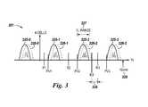
- FIG. 3illustrates a diagram 301 of a change in read voltage threshold distributions for programmed states based on a length of time after programming in accordance with a number of embodiments of the present disclosure.
- the example shown in FIG. 3can represent, for example, memory cells 110 - 1 , . . . , 110 -N previously described in connection with FIG. 1 .
- the example shown in FIG. 3represents two-bit, e.g., four-state, memory cells. However, embodiments of the present disclosure are not limited to this example of two-bit memory cells.
- FIG. 3illustrates a diagram of read voltage threshold distributions for programmed states in accordance with a number of embodiments of the present disclosure.
- the example shown in FIG. 3can represent, for example, memory cells 110 - 1 , . . . , 110 -N previously described in connection with FIG. 1 .
- the example shown in FIG. 3represents two-bit, e.g., four-state, memory cells.
- embodiments of the present disclosureare not limited to this example of two-bit memory cells.
- FIG. 3shows threshold voltage (Vt) distributions that represent four target states, e.g., L0, L1, L2, and L3, respectively, to which the memory cells can be programmed.
- Threshold voltage (Vt) distributions 325 - 0 , 325 - 1 , 325 - 2 , and 325 - 3correspond to each of the four target states.
- Threshold voltage (Vt) distributions 326 - 0 , 326 - 1 , 326 - 2 , and 326 - 3(shown in FIG.
- Vtthreshold voltage
- the memory cells in a selected blockcan be erased together such that they have a Vt level within Vt distribution 325 - 0 prior to being programmed.
- distribution 325 - 0can be referred to as an erased state and can represent a particular stored data state (target state L0), e.g., stored data such as binary “11”.
- Target data state L1can correspond to data 01
- target data state L2can correspond to data 00
- target data state L3can correspond to data 10.
- sensing voltagesare illustrated in FIG. 3 .
- Such sensing voltagescan include program verify voltages (e.g., PV 1 , PV 2 , PV 3 ) and/or read voltages (R 1 , R 2 , R 3 ).
- Voltage levels R 1 , R 2 , and R 3represent sensing voltages, e.g., read voltages, that can be used to distinguish between states L0, L1, L2, and L3 during a sensing operation.
- the unselected memory cells of the stringcan be biased with a pass voltage “Vpass” 329 so as to be in a conducting state.
- FIG. 3also shows a read voltage R 3 ′, which can be a reduced read voltage for pages subsequent to the last written page when determined that an asynchronous power loss did not occur during final programming of the last written page and therefore may have occurred during an early stage of programming one or more pages subsequent to the last written page.
- the alternate read voltage, R 3 ′can be reduced from a default read voltage (e.g., R 3 ) by a pre-determined voltage amount 328 .
- a reduced read voltageis illustrated in FIG. 3 for only one read level, R 3 , the other read levels, R 1 and/or R 2 , can also be reduced for performing a check pages subsequent to the last written page, as previously described.
- FIG. 4is a flow chart illustrating a method of operating memory in accordance with a number of embodiments of the present disclosure.
- the memorycan check whether a prior power loss was an asynchronous power loss. For example, the memory can look for an indication that the prior power loss was initiated by the host computing system (e.g., host 102 illustrated in FIG. 1 ). The absence of such indication can cause the memory to proceed with testing associated with asynchronous power loss such a Vt margin analysis. If the prior power loss was not an asynchronous power loss, the memory can proceed with programming a page subsequent to the last written page, as indicated at 474 in FIG. 4 , since the last written page was properly programmed where shut down of the memory was orderly.
- the host computing systeme.g., host 102 illustrated in FIG. 1
- the memorycan identify the last written page and determine whether errors associated with the last written page are ECC correctible, as shown at 462 in FIG. 4 . If the errors of the last written page are not ECC correctible, correction action can be taken in response, such as to stop using the block corresponding to the page having the ECC uncorrectable errors and/or programming dummy data to the last written page (and/or subsequent pages(s)), as shown at 464 in FIG. 4 .
- the last written pagecan be tested with increased read voltage (e.g., increased lower page read voltage) to determine whether RWB margin is adequate, as shown at 466 .
- increased read voltagee.g., increased lower page read voltage
- the corrective action shown at 468 and discussed abovecan be implemented to address the inadequate RWB.
- RWB margin of the last written pageis adequate when the last written page is tested with an increased read voltage (indicating the asynchronous power loss did not occur during a final stage of programming the last written page)
- one or more actionscan be taken with respect to pages subsequent to the last written page.
- one actioncan involve using a reduced read voltage for one or more pages subsequent to the last written page.
- Another actioncan involve implementing a source shifting to increase Vt by a predetermined amount for one or more pages subsequent to the last written page, as shown at 472 in FIG. 4 .
- correction actioncan be taken in response, such as to stop using the block corresponding to the page having the ECC uncorrectable errors and/or programming dummy data to the last written page (and/or subsequent pages(s)), as shown at 464 in FIG. 4 .
- the memorycan proceed with programming a page subsequent to the last written page, as indicated at 474 in FIG. 4 .
Landscapes
- Engineering & Computer Science (AREA)
- Theoretical Computer Science (AREA)
- Quality & Reliability (AREA)
- Physics & Mathematics (AREA)
- General Engineering & Computer Science (AREA)
- General Physics & Mathematics (AREA)
- Power Engineering (AREA)
- Read Only Memory (AREA)
Abstract
Description
- This application claims benefit of priority under 35 U.S.C. 119(e) to U.S. Provisional Application Ser. No. 62/068,364, filed Oct. 24, 2014, the specification of which is incorporated herein by reference.
- The present disclosure relates generally to semiconductor memory and methods, and more particularly, to memory cell threshold voltage margin analysis.
- Memory devices are typically provided as internal, semiconductor, integrated circuits in computers or other electronic devices. There are many different types of memory including volatile and non-volatile memory. Volatile memory can require power to maintain its data (e.g., host data, error data, etc.) and includes random-access memory (RAM), dynamic random access memory (DRAM), and synchronous dynamic random access memory (SDRAM), among others. Non-volatile memory can provide persistent data by retaining stored data when not powered and can include NAND flash memory, NOR flash memory, read only memory (ROM), Electrically Erasable Programmable ROM (EEPROM), Erasable Programmable ROM (EPROM), and resistance variable memory such as phase change random access memory (PCRAM), resistive random access memory (RRAM), and magnetoresistive random access memory (MRAM), among others.
- Memory devices can be combined together to form a storage volume of a memory system such as a solid state drive (SSD). A solid state drive can include non-volatile memory (e.g., NAND flash memory and NOR flash memory), and/or can include volatile memory (e.g., DRAM and SRAM), among various other types of non-volatile and volatile memory. Memory is used herein to refer to a group of memory cells, which may be arranged as a memory array, a memory device, a memory system, or other one of various configurations.
- An SSD can be used to replace hard disk drives as the main storage volume for a computer, as the solid state drive can have advantages over hard drives in terms of performance, size, weight, ruggedness, operating temperature range, and power consumption. For example, SSDs can have superior performance when compared to magnetic disk drives due to their lack of moving parts, which may avoid seek time, latency, and other electro-mechanical delays associated with magnetic disk drives.
- Upon power loss while writing data to a memory device, memory cells can be left in an uncertain condition. Memory can have memory cells that are partially (e.g., shallowly) programmed but appears to be erased. Memory can have memory cells that are incompletely programmed to within a target threshold voltage range of an intended data state but perhaps only barely within so as to marginally pass a verification read. Memory can have memory cells that are insufficiently programmed with respect to the target threshold voltage range of the intended data state, which can result in Error Correction Code (ECC) errors. Condition of memory cells in progress of being programmed when a power loss occurs can vary depending on the data state being programmed, location of the memory cell with respect to an upper page, lower page, even page, odd page, and number of data states to which the memory cell is being programmed, among others. Upon power-up, the various conditions of the memory cells of the memory can affect data integrity of the memory device and performance of the host computing system in different ways.
- Detection of a number of ECC errors associated with a memory can result in the host computing system identifying a portion of the memory (e.g., page) as being corrupted, which can cause the host computing system to waste time and energy attempting to correct the ECC errors and/or unnecessarily stop using the portion of the memory. Memory that has memory cells that are shallowly programmed (e.g., not fully erased) but appear to be erased can be sensitive to Program Disturb if the host computing system attempts to program new data to the memory cells on top of the shallowly programmed condition of the memory cells. Memory cells that are incompletely programmed within a threshold voltage range but pass a verification read can be more susceptible to data retention issues under certain conditions such as at higher temperatures.
- Power loss while erasing data from a memory (e.g., programming a memory cell to an erase state) can result in partially erased pages that are susceptible to Disturb and misplacement. Accordingly, apparatus and methods to assess and address memory cell conditions following a power loss can improve operation of a memory device.
FIG. 1 is a block diagram of an apparatus in the form of a computing system including at least one memory system in accordance with a number of embodiments of the present disclosure.FIG. 2 illustrates a schematic diagram of a portion of a non-volatile memory array in accordance with a number of embodiments of the present disclosure.FIG. 3 illustrates a diagram of read voltage threshold distributions for programmed states in accordance with a number of embodiments of the present disclosure.FIG. 4 is a flow chart illustrating a method of operating memory in accordance with a number of embodiments of the present disclosure.- The present disclosure is related to a threshold voltage margin analysis. An example embodiment apparatus can include a memory and a controller coupled to the memory. The controller is configured to determine a previous power loss of a memory to be an asynchronous power loss, and identify a portion of the memory last subject to programming operations during the determined asynchronous power loss. The controller is further configured to perform a threshold voltage (Vt) margin analysis on the portion of the memory responsive to the determined asynchronous power loss.
- According to various embodiments of the present disclosure, recovery from a power loss can include performing a threshold voltage (Vt) margin analysis to determine whether a particular portion of memory (e.g., a page, block, etc.) can be used for data operations (e.g., READ, programming such as WRITE, erase, etc.). Vt margin analysis performed after a power loss can be used to assess a condition of a particular portion of memory can mitigate data loss, help to avoid premature block retirement, and improve overall system performance by minimizing the time and energy associated with misguide corrective actions due to misdiagnosed and undiagnosed memory conditions. According to some embodiments, Vt margin analysis can be performed after a power loss to determine if a read window budget is adequate when a last written page is tested with increased read voltage.
- Ideally a host computing system in communication with a memory, such as a NAND Flash based memory device, can notify a memory controller prior to an imminent power loss with sufficient lead time ahead of the power loss. In this manner, the memory device can exit in-progress operations in an orderly fashion. However, there can be occasions when power to the memory is abruptly disconnected, a scenario commonly referred to as an asynchronous power loss.
- One previous hardware approach for facilitating an orderly shutdown of a memory in response to an imminent power loss is to provide sufficient hold-up capacitance to provide energy for accomplishing an orderly power down of the memory. For example, a memory device can comprise a hold-up capacitance of sufficient size to provide the necessary stored energy to allow the memory to conclude in-progress operations. However, the cost of this hardware approach includes the additional expense for hold-up capacitance and increased hardware footprint occupied by the hold-up capacitance.
- A power loss initiated by a host computing system can provide an indication (e.g., imprint) to a memory to indicate to the memory that the previous power down was initiated by the host, and thus orderly. Without this indication, the memory can proceed based on a previous power loss being an asynchronous power loss. Such an indication can be checked for by the memory upon power-up. Absent such an indication, the memory can proceed to determine whether any programming operations were in-process at the time of that power loss that left the memory in an uncertain or incorrect condition.
- Where memory device cost and/or size are more important considerations, such as for solid state drive (SSD) and smaller form factor NAND FLASH modules, providing hold-up capacitance can be an infeasible solution for managing sudden power loss. However, without hold-up capacitance an orderly power down of the memory may not be possible. If the memory is in-process of certain programming operations at the time of power loss (e.g., WRITE operation, ERASE operation, etc.) some portions (e.g., pages) of the memory can be left in an incompletely programmed and/or unstable condition. Continuing to use these portions of the memory device can create uncorrectable failures, trigger unnecessary retirement of portions of the memory device (e.g., blocks), and force the memory device to implement WRITE protect techniques.
- Memory device programming operations can be performed in steps (e.g., via multiple programming pulses). The time to complete program and erase operations can range from several hundred micro-seconds to a few milliseconds. The Vt state of a page can be a strong function of the point during a programming operation at which the power loss occurred. In the case of programming operations, if the power loss happens during an early stage of programming, pages can be partially programmed but read as erased (e.g., blank) pages by the memory controller (e.g., firmware). Continuing to use these partially-programmed pages can result in Disturb, and the page can be at increased risk of misplacement. If the power loss happens during a later stage of programming, the Vt of the pages may have reached an intended data state but the Read Window Budget (RWB) margins can be weaker resulting in data retention issues.
- If the power loss happens during an intermediate stage of programming, then the Vt can be in disarray resulting in uncorrectable errors (e.g., uncorrectable error correction code (ECC) errors). Power loss during an intermediate stage of programming can be detected by the memory controller, which can trigger corrective action. However, power loss during initial and/or later stage of programming may not be detected using default read voltages, which can result in reliability issues when these pages are subsequently used for READ operations and/or programming operations.
- If a power loss happens during an erase operation, the Vt of a memory cell can be in an incompletely erased state with the memory cell appearing to be erased. The consequences of such memory cell condition are similar to those associated with power loss during an early stage of programming previously described. Risks associated with memory cells not being fully programmed to an intended data or erased state can also increase proportional to the number of bits stored per memory cell since RWBs shrink as the number of Vt levels per memory cell increase.
- According to some embodiments, a memory controller can be configured to identify a portion of the memory last subject to erase operations at the time of an asynchronous power loss, and perform a threshold voltage (Vt) margin analysis with respect to an erased state on the portion of the memory. For example, the controller can be configured to determine that the portion of the memory is indicated as being erased and that the portion of the memory is not fully programmed to the erased state. Similar to performing a Vt margin analysis on a last written page, a memory controller can be configured to perform an erase verify operation on the portion of the memory using a read voltage that is different (e.g., less) than a default erase verify operation read voltage, in order to determine whether a read window budget (RWB) associated with the erased data state is adequate. The controller can also be configured to increase the Vt for programming operations associated with the portion of the memory by a predetermined amount.
- The present disclosure provides an effective way to accurately determine whether memory operations were in-process, and if an abrupt power down has left the memory in unstable or uncertain Vt state. According to various embodiments, the controller can initially scan for the last written page (LWP) on the memory. If the last written page is ECC correctible, then the power loss may have happened at the final stage of programming. If there is adequate read window budget (RWB) margin when the LWP is tested with increased read voltage, a check can be performed, for example, by increasing the Lower Page read voltage by a pre-determined voltage amount or percentage to determine. If the LWP looks normal for the check, then one conclusion is that power loss did not happen during a final stage of programming.
- If power loss did not happen during a final stage of programming, whether the power loss happened during the early stage of programming of one a page subsequent to LWP can be investigated. For instance, one or more pages subsequent to the LWP can be checked using a read voltage that is reduced from a default value. According to some embodiments, one or more pages subsequent to the LWP can be checked using a read voltage adjusted to a lowest possible voltage corresponding to a particular data state. Also, a source shift can be implemented to increase the Vt of a portion (e.g., entire page) by a pre-determined voltage value or percentage.
- This source shift approach provides an extra guard band in the Vt in the vicinity of a data state in order to weed out portions of memory (e.g., one or more pages) that may be incompletely programmed but look as if in an erased state. Any uncorrectable error during the above-mentioned check(s) can be considered a probable candidate that an asynchronous power loss occurred while memory WRITE/ERASE operations were in-process. The memory and/or host computing system can take corrective actions such as to stop using the portion of memory (e.g., block), or can program dummy data on at least the pages determined as being affected by power loss and/or additional pages as a precaution. This approach helps preserve the RWB margins, minimize the misplacement, and ensure data integrity.
- In the following detailed description of the present disclosure, reference is made to the accompanying drawings that form a part hereof, and in which is shown by way of illustration how a number of embodiments of the disclosure may be practiced. These embodiments are described in sufficient detail to enable those of ordinary skill in the art to practice the embodiments of this disclosure, and it is to be understood that other embodiments may be utilized and that process, electrical, and/or structural changes may be made without departing from the scope of the present disclosure. As used herein, the designators “N” and “M”, particularly with respect to reference numerals in the drawings, indicates that a number of the particular feature so designated can be included. As used herein, “a number of” a particular thing can refer to one or more of such things (e.g., a number of memory devices can refer to one or more memory devices).
- The figures herein follow a numbering convention in which the first digit or digits correspond to the drawing figure number and the remaining digits identify an element or component in the drawing. Similar elements or components between different figures may be identified by the use of similar digits. For example,321 may reference element “21” in
FIG. 3 , and a similar element may be referenced as421 inFIG. 4 . As will be appreciated, elements shown in the various embodiments herein can be added, exchanged, and/or eliminated so as to provide a number of additional embodiments of the present disclosure. In addition, as will be appreciated, the proportion and the relative scale of the elements provided in the figures are intended to illustrate certain embodiments of the present invention, and should not be taken in a limiting sense. FIG. 1 is a block diagram of an apparatus in the form of acomputing system 100 including at least onememory system 104 in accordance with a number of embodiments of the present disclosure. As used herein, amemory system 104, acontroller 108, or amemory device 110 might also be separately considered an “apparatus.” Thememory system 104 can be a solid state drive (SSD), for instance, and can include ahost interface 106, a controller108 (e.g., a processor and/or other control circuitry), and a number of memory devices110-1, . . . ,110-N (e.g., solid state memory devices such as charge-trapping NAND flash devices), which provide a storage volume for thememory system 104. Thememory system 104 can be a single memory device.- As illustrated in
FIG. 1 , thecontroller 108 can be coupled to thehost interface 106 and to the memory devices110-1, . . . ,110-N via a plurality of channels and can be used to send data between thememory system 104 and ahost 102. A hold-upcapacitance 128 may be coupled to thecontroller 108 and/or memory devices110-1, . . . ,110-N. The hold-upcapacitance 128 may or may not be sufficient to provide enough energy for an orderly shut-down in the event of every power loss scenario. According to some embodiments of the present disclosure, thememory system 104 can be devoid of any hold-upcapacitance 128. - The
interface 106 can be in the form of a standardized interface. For example, when thememory system 104 is used for data storage in acomputing system 100, theinterface 106 can be a serial advanced technology attachment (SATA), peripheral component interconnect express (PCIe), or a universal serial bus (USB), among other connectors and interfaces. In general, however,interface 106 can provide an interface for passing control, address, data, and other signals between thememory system 104 and ahost 102 having compatible receptors for theinterface 106. - Host102 can be a host system such as a personal laptop computer, a desktop computer, a digital camera, a mobile telephone, or a memory card reader, among various other types of hosts. Host102 can include a system motherboard and/or backplane and can include a number of memory access devices (e.g., a number of processors). Host102 can also be a memory controller, such as where
memory system 104 is a memory device (e.g., having an on-die controller). - The
controller 108 can communicate with the memory devices110-1, . . . ,110-N to control data READ, WRITE, and erase operations, among other operations. The memory devices110-1, . . . ,110-N can include a plurality ofmemory arrays 107 on a single die, a plurality ofmemory arrays 107 on multiple dies, or asingle memory array 107 on a single die. Thecontroller 108 can be on the same die or a different die than any or all of the memory devices110-1, . . . ,110-N. FIG. 2 illustrates a schematic diagram of a portion of a non-volatile memory array in accordance with a number of embodiments of the present disclosure. The memory array can be contained within the memory devices110-1, . . . ,110-N illustrated inFIG. 1 . The embodiment ofFIG. 2 illustrates a NAND architecture non-volatile memory array. However, embodiments described herein are not limited to this example. As shown inFIG. 2 , the memory array201 includes access lines (e.g., word lines205-1, . . . ,205-N) and intersecting data lines (e.g., local bit lines207-1,207-2,207-3, . . . ,207-M). For ease of addressing in the digital environment, the number of word lines205-1, . . . ,205-N and the number of local bit lines207-1,207-2,207-3, . . . ,207-M can be some power of two (e.g., 256 word lines by 4,096 bit lines).- Memory array201 includes NAND strings209-1,209-2,209-3, . . . ,209-M. Each NAND string includes non-volatile memory cells211-1, . . . ,211-N, each communicatively coupled to a respective word line205-1, . . . ,205-N. Each NAND string (and its constituent memory cells) is also associated with a local bit line207-1,207-2,207-3, . . . ,207-M. The memory cells211-1, . . . ,211-N of each NAND string209-1,209-2,209-3, . . . ,209-M are coupled in series source to drain between a source select gate (SGS) (e.g., a field-effect transistor (FET)213) and a drain select gate (SGD) (e.g., FET219). Each source
select gate 213 is configured to selectively couple a respective NAND string to a common source223 responsive to a signal on sourceselect line 217, while each drainselect gate 219 is configured to selectively couple a respective NAND string to a respective bit line responsive to a signal on drainselect line 215. - As shown in the embodiment illustrated in
FIG. 2 , a source of sourceselect gate 213 is coupled to a common source line223. The drain of sourceselect gate 213 is coupled to the source of the memory cell211-1 of the corresponding NAND string209-1. The drain of drainselect gate 219 is coupled to bit line207-1 of the corresponding NAND string209-1 at drain contact221-1. The source of drainselect gate 219 is coupled to the drain of the last memory cell211-N (e.g., a floating-gate transistor) of the corresponding NAND string209-1. - In a number of embodiments, construction of the non-volatile memory cells211-1, . . . ,211-N includes a source, a drain, a floating gate or other charge storage structure, and a control gate. The memory cells211-1, . . . ,211-N have their control gates coupled to a word line,205-1, . . . ,205-N, respectively. A NOR array architecture would be similarly laid out, except that the string of memory cells would be coupled in parallel between the select gates. Furthermore, a NOR architecture can provide for random access to the memory cells in the array (e.g., as opposed to page-based access as with a NAND architecture).
- A number (e.g., a subset or all) of cells coupled to a selected word line (e.g.,205-1, . . . ,205-N) can be written and/or read together as a group. A number of cells written and/or read together can correspond to a page of data. As used herein, examples of high-level operations are referred to as writing or reading operations (e.g., from the perspective of a controller), whereas, with respect to the memory cells, such operations are referred to as programming or sensing. A group of cells coupled to a particular word line and programmed together to respective states can be referred to as a target page. A programming operation can include applying a number of program pulses (e.g., 16V-20V) to a selected word line in order to increase the threshold voltage (Vt) of selected cells coupled to that selected word line to a desired program voltage level corresponding to a targeted state.
- Read operations can include sensing a voltage and/or current change of a bit line coupled to a selected cell in order to determine the state of the selected cell. The read operation can include precharging a bit line and sensing the discharge when a selected cell begins to conduct. Two different types of read operations are described herein (e.g., those using a ramping read signal versus using a plurality of discrete read signals).
- Sensing the state of a selected cell can include providing a ramping read signal (e.g., −2V to +3V) to a selected word line, while providing a signal (e.g., a pass voltage such as 4.5V) to word lines coupled to the unselected cells of the string sufficient to place the unselected cells in a conducting state independent of the charge stored on the unselected cells. Alternatively, sensing the state of a selected cell could include applying discrete read signal levels (e.g., −0.05V, 0.5V, and 2V) to a selected word line, and thus to the control gate of a selected cell. The bit line corresponding to the selected cell being read and/or verified can be sensed to determine whether or not the selected cell conducts in response to the particular read signal applied to the selected word line. For example, the state of a selected cell can be determined by the word line voltage at which the bit line current reaches a particular reference current associated with a particular state.
FIG. 3 illustrates a diagram301 of a change in read voltage threshold distributions for programmed states based on a length of time after programming in accordance with a number of embodiments of the present disclosure. The example shown inFIG. 3 can represent, for example, memory cells110-1, . . . ,110-N previously described in connection withFIG. 1 . The example shown inFIG. 3 represents two-bit, e.g., four-state, memory cells. However, embodiments of the present disclosure are not limited to this example of two-bit memory cells.FIG. 3 illustrates a diagram of read voltage threshold distributions for programmed states in accordance with a number of embodiments of the present disclosure. The example shown inFIG. 3 can represent, for example, memory cells110-1, . . . ,110-N previously described in connection withFIG. 1 . The example shown inFIG. 3 represents two-bit, e.g., four-state, memory cells. However, embodiments of the present disclosure are not limited to this example of two-bit memory cells.FIG. 3 shows threshold voltage (Vt) distributions that represent four target states, e.g., L0, L1, L2, and L3, respectively, to which the memory cells can be programmed. Threshold voltage (Vt) distributions325-0,325-1,325-2, and325-3 (shown inFIG. 3 using solid lines) correspond to each of the four target states. Threshold voltage (Vt) distributions326-0,326-1,326-2, and326-3 (shown inFIG. 3 using dotted lines) correspond to each of the four target states after source shifting is implemented, which shifts the threshold voltage (Vt) distributions to increased voltage levels (e.g., for pages subsequent to the last written page when determined that an asynchronous power loss did not occur during final programming of the last written page and therefore may have occurred during an early stage of programming one or more pages subsequent to the last written page.- In operation, the memory cells in a selected block can be erased together such that they have a Vt level within Vt distribution325-0 prior to being programmed. As such, distribution325-0 can be referred to as an erased state and can represent a particular stored data state (target state L0), e.g., stored data such as binary “11”. Target data state L1 can correspond to data 01, target data state L2 can correspond to
data 00, and target data state L3 can correspond todata 10. - A number of sensing voltages are illustrated in
FIG. 3 . Such sensing voltages can include program verify voltages (e.g., PV1, PV2, PV3) and/or read voltages (R1, R2, R3). Voltage levels R1, R2, and R3 represent sensing voltages, e.g., read voltages, that can be used to distinguish between states L0, L1, L2, and L3 during a sensing operation. In a sensing operation performed on a selected memory cell in a memory, the unselected memory cells of the string can be biased with a pass voltage “Vpass”329 so as to be in a conducting state. FIG. 3 also shows a read voltage R3′, which can be a reduced read voltage for pages subsequent to the last written page when determined that an asynchronous power loss did not occur during final programming of the last written page and therefore may have occurred during an early stage of programming one or more pages subsequent to the last written page. The alternate read voltage, R3′, can be reduced from a default read voltage (e.g., R3) by apre-determined voltage amount 328. Although a reduced read voltage is illustrated inFIG. 3 for only one read level, R3, the other read levels, R1 and/or R2, can also be reduced for performing a check pages subsequent to the last written page, as previously described.FIG. 4 is a flow chart illustrating a method of operating memory in accordance with a number of embodiments of the present disclosure. At460 the memory can check whether a prior power loss was an asynchronous power loss. For example, the memory can look for an indication that the prior power loss was initiated by the host computing system (e.g., host102 illustrated inFIG. 1 ). The absence of such indication can cause the memory to proceed with testing associated with asynchronous power loss such a Vt margin analysis. If the prior power loss was not an asynchronous power loss, the memory can proceed with programming a page subsequent to the last written page, as indicated at474 inFIG. 4 , since the last written page was properly programmed where shut down of the memory was orderly.- If the prior power loss was an asynchronous power loss, the memory can identify the last written page and determine whether errors associated with the last written page are ECC correctible, as shown at462 in
FIG. 4 . If the errors of the last written page are not ECC correctible, correction action can be taken in response, such as to stop using the block corresponding to the page having the ECC uncorrectable errors and/or programming dummy data to the last written page (and/or subsequent pages(s)), as shown at464 inFIG. 4 . - If errors associated with the last written page are ECC correctible, the last written page can be tested with increased read voltage (e.g., increased lower page read voltage) to determine whether RWB margin is adequate, as shown at466. When RWB margin of the last written page is not adequate, the corrective action shown at468 and discussed above can be implemented to address the inadequate RWB. Otherwise, when RWB margin of the last written page is adequate when the last written page is tested with an increased read voltage (indicating the asynchronous power loss did not occur during a final stage of programming the last written page), one or more actions can be taken with respect to pages subsequent to the last written page.
- As shown at470 in
FIG. 4 , one action can involve using a reduced read voltage for one or more pages subsequent to the last written page. Another action can involve implementing a source shifting to increase Vt by a predetermined amount for one or more pages subsequent to the last written page, as shown at472 inFIG. 4 . Thereafter, it can be determined whether one or more pages subsequent to the last written page are reading as an empty page(s). If not reading as an empty page(s), correction action can be taken in response, such as to stop using the block corresponding to the page having the ECC uncorrectable errors and/or programming dummy data to the last written page (and/or subsequent pages(s)), as shown at464 inFIG. 4 . If the one or more pages subsequent to the last written page are reading as an empty page(s), the memory can proceed with programming a page subsequent to the last written page, as indicated at474 inFIG. 4 . - Although specific embodiments have been illustrated and described herein, those of ordinary skill in the art will appreciate that an arrangement calculated to achieve the same results can be substituted for the specific embodiments shown. This disclosure is intended to cover adaptations or variations of a number of embodiments of the present disclosure. It is to be understood that the above description has been made in an illustrative fashion, and not a restrictive one. Combination of the above embodiments, and other embodiments not specifically described herein will be apparent to those of skill in the art upon reviewing the above description. The scope of the number of embodiments of the present disclosure includes other applications in which the above structures and methods are used. Therefore, the scope of a number of embodiments of the present disclosure should be determined with reference to the appended claims, along with the full range of equivalents to which such claims are entitled.
- In the foregoing Detailed Description, some features are grouped together in a single embodiment for the purpose of streamlining the disclosure. This method of disclosure is not to be interpreted as reflecting an intention that the disclosed embodiments of the present disclosure have to use more features than are expressly recited in each claim. Rather, as the following claims reflect, inventive subject matter lies in less than all features of a single disclosed embodiment. Thus, the following claims are hereby incorporated into the Detailed Description, with each claim standing on its own as a separate embodiment.
Claims (36)
Priority Applications (2)
| Application Number | Priority Date | Filing Date | Title |
|---|---|---|---|
| US14/681,618US9728278B2 (en) | 2014-10-24 | 2015-04-08 | Threshold voltage margin analysis |
| US15/642,410US10418122B2 (en) | 2014-10-24 | 2017-07-06 | Threshold voltage margin analysis |
Applications Claiming Priority (2)
| Application Number | Priority Date | Filing Date | Title |
|---|---|---|---|
| US201462068364P | 2014-10-24 | 2014-10-24 | |
| US14/681,618US9728278B2 (en) | 2014-10-24 | 2015-04-08 | Threshold voltage margin analysis |
Related Child Applications (1)
| Application Number | Title | Priority Date | Filing Date |
|---|---|---|---|
| US15/642,410ContinuationUS10418122B2 (en) | 2014-10-24 | 2017-07-06 | Threshold voltage margin analysis |
Publications (2)
| Publication Number | Publication Date |
|---|---|
| US20160118143A1true US20160118143A1 (en) | 2016-04-28 |
| US9728278B2 US9728278B2 (en) | 2017-08-08 |
Family
ID=55792513
Family Applications (2)
| Application Number | Title | Priority Date | Filing Date |
|---|---|---|---|
| US14/681,618Active2035-11-12US9728278B2 (en) | 2014-10-24 | 2015-04-08 | Threshold voltage margin analysis |
| US15/642,410Active2035-08-12US10418122B2 (en) | 2014-10-24 | 2017-07-06 | Threshold voltage margin analysis |
Family Applications After (1)
| Application Number | Title | Priority Date | Filing Date |
|---|---|---|---|
| US15/642,410Active2035-08-12US10418122B2 (en) | 2014-10-24 | 2017-07-06 | Threshold voltage margin analysis |
Country Status (1)
| Country | Link |
|---|---|
| US (2) | US9728278B2 (en) |
Cited By (12)
| Publication number | Priority date | Publication date | Assignee | Title |
|---|---|---|---|---|
| CN107766260A (en)* | 2016-08-19 | 2018-03-06 | 爱思开海力士有限公司 | Memory device, there is its storage system and its operating method |
| US9921898B1 (en) | 2016-12-27 | 2018-03-20 | Micron Technology, Inc. | Identifying asynchronous power loss |
| WO2019045921A1 (en)* | 2017-08-31 | 2019-03-07 | Micron Technology, Inc. | Responding to power loss |
| US10282110B2 (en)* | 2016-04-08 | 2019-05-07 | SK Hynix Inc. | Last written page indicator |
| CN110147332A (en)* | 2018-02-13 | 2019-08-20 | 纬颖科技服务股份有限公司 | The management method and memory device of catalogue data |
| US10418122B2 (en)* | 2014-10-24 | 2019-09-17 | Micron Technology, Inc. | Threshold voltage margin analysis |
| CN111324549A (en)* | 2018-12-14 | 2020-06-23 | 北京兆易创新科技股份有限公司 | Memory and control method and device thereof |
| CN113421601A (en)* | 2021-06-29 | 2021-09-21 | 长江存储科技有限责任公司 | Flash memory and operation method thereof |
| US11366592B2 (en)* | 2020-08-31 | 2022-06-21 | Micron Technology, Inc. | Selective dummy writes for asynchronous power loss handling in memory devices |
| US11443817B2 (en)* | 2020-01-28 | 2022-09-13 | Samsung Electronics Co., Ltd. | Nonvolatile memory device |
| US20240170090A1 (en)* | 2022-11-22 | 2024-05-23 | Micron Technology, Inc. | Power loss error detection using partial block handling |
| WO2025128201A1 (en)* | 2023-12-14 | 2025-06-19 | SK hynix NAND Product Solutions Corporation | Systems, methods, and media for recovering non-volatile memory devices from power loss |
Families Citing this family (6)
| Publication number | Priority date | Publication date | Assignee | Title |
|---|---|---|---|---|
| JP2020047339A (en)* | 2018-09-18 | 2020-03-26 | キオクシア株式会社 | Memory system |
| US10614898B1 (en)* | 2018-09-19 | 2020-04-07 | Sandisk Technologies Llc | Adaptive control of memory cell programming voltage |
| US10872639B2 (en) | 2018-12-31 | 2020-12-22 | Micron Technology, Inc. | Recovery of memory from asynchronous power loss |
| KR102610395B1 (en) | 2019-01-22 | 2023-12-05 | 삼성전자주식회사 | Memory system comprising non-volatile memory device |
| KR102632690B1 (en) | 2019-06-13 | 2024-02-01 | 삼성전자주식회사 | Nonvolatile memory device and the method for programing the same |
| US20250004647A1 (en)* | 2023-06-29 | 2025-01-02 | Micron Technology, Inc. | Reliability improvements using memory die binning |
Citations (31)
| Publication number | Priority date | Publication date | Assignee | Title |
|---|---|---|---|---|
| US5973957A (en)* | 1997-09-16 | 1999-10-26 | Intel Corporation | Sense amplifier comprising a preamplifier and a differential input latch for flash memories |
| US6243839B1 (en)* | 1996-01-22 | 2001-06-05 | Micron Technology, Inc. | Non-volatile memory system including apparatus for testing memory elements by writing and verifying data patterns |
| US6634004B1 (en)* | 2000-04-28 | 2003-10-14 | Mitsubishi Denki Kabushiki Kaisha | Threshold analysis system capable of deciding all threshold voltages included in memory device through single processing |
| US20060062049A1 (en)* | 2004-09-17 | 2006-03-23 | Seok-Heon Lee | Methods for programming user data and confirmation information in nonvolatile memory devices |
| US7254757B2 (en)* | 2003-11-12 | 2007-08-07 | Samsung Electronics Co., Ltd. | Flash memory test system and method capable of test time reduction |
| US7319615B1 (en)* | 2006-08-02 | 2008-01-15 | Spansion Llc | Ramp gate erase for dual bit flash memory |
| US20080195903A1 (en)* | 2007-02-14 | 2008-08-14 | Qimonda Flash Gmbh & Co. Kg | Non-volatile memory device with built-in test control unit and methods of testing and repairing a cell array |
| US20080307373A1 (en)* | 2007-05-02 | 2008-12-11 | Sony Corporation | Apparatus, method and computer program for managing circuit optimization information |
| US20100082177A1 (en)* | 2008-10-01 | 2010-04-01 | Korea Electric Power Corporation | System and Method For Controlling Multiple Facts |
| US7747900B2 (en)* | 2007-04-02 | 2010-06-29 | International Business Machines Corporation | Thresholding system power loss notifications in a data processing system based on vital product data |
| US20110150060A1 (en)* | 2009-12-23 | 2011-06-23 | Sun Microsystems, Inc. | Voltage Margin Monitoring for an ADC-Based Serializer/Deserializer in Mission Mode |
| US20110278949A1 (en)* | 2011-02-01 | 2011-11-17 | Tsai Ming-Chiu | High-power induction-type power supply system and its data transmission method |
| US20120041696A1 (en)* | 2010-08-10 | 2012-02-16 | Sensus Usa Inc. | Electric Utility Meter To Stimulate Enhanced Functionality |
| US20120101640A1 (en)* | 2009-01-30 | 2012-04-26 | Dewind Co. | Adaptive voltage control for wind turbines |
| US8179718B2 (en)* | 2008-07-04 | 2012-05-15 | Samsung Electronics Co., Ltd. | Memory device and memory programming method |
| US8243513B2 (en)* | 2007-05-02 | 2012-08-14 | Micron Technology, Inc. | Non-volatile multilevel memory cells with data read of reference cells |
| US8291297B2 (en)* | 2008-12-18 | 2012-10-16 | Intel Corporation | Data error recovery in non-volatile memory |
| US8365030B1 (en)* | 2009-03-30 | 2013-01-29 | Samsung Electronics Co., Ltd. | Nonvolatile memory devices and error correction methods thereof |
| US20130047132A1 (en)* | 2011-08-16 | 2013-02-21 | Samsung Electronics Co., Ltd. | Method of designing nonvolatile memory device |
| US20130054871A1 (en)* | 2011-08-26 | 2013-02-28 | Paul A. Lassa | Controller with extended status register and method of use therewith |
| US20140223399A1 (en)* | 2013-02-01 | 2014-08-07 | Fujitsu Limited | Circuit analysis device and circuit analysis method |
| US20140304560A1 (en)* | 2007-08-30 | 2014-10-09 | HGST, Inc. | Shutdowns and data recovery to avoid read errors weak pages in a non-volatile memory system |
| US20140365146A1 (en)* | 2013-06-11 | 2014-12-11 | Control4 Corporation | Systems and methods for investigating a load and obtaining load information |
| US9037946B2 (en)* | 2013-03-12 | 2015-05-19 | Sandisk Technologies Inc. | Detecting effect of corrupting event on preloaded data in non-volatile memory |
| US9142296B2 (en)* | 2012-08-27 | 2015-09-22 | SK Hynix Inc. | Nonvolatile memory device and method for driving the same |
| US9245653B2 (en)* | 2010-03-15 | 2016-01-26 | Intelligent Intellectual Property Holdings 2 Llc | Reduced level cell mode for non-volatile memory |
| US20160048150A1 (en)* | 2014-08-14 | 2016-02-18 | Bigwood Technology, Inc. | Method and apparatus for optimal power flow with voltage stability for large-scale electric power systems |
| US20160070336A1 (en)* | 2014-09-10 | 2016-03-10 | Kabushiki Kaisha Toshiba | Memory system and controller |
| US20160099078A1 (en)* | 2014-10-02 | 2016-04-07 | Sandisk Technologies Inc. | Data storage device having reflow awareness |
| US20160211033A1 (en)* | 2013-08-13 | 2016-07-21 | Empire Technology Development Llc | Memory systems |
| US9454420B1 (en)* | 2012-12-31 | 2016-09-27 | Sandisk Technologies Llc | Method and system of reading threshold voltage equalization |
Family Cites Families (48)
| Publication number | Priority date | Publication date | Assignee | Title |
|---|---|---|---|---|
| JPH0773685A (en) | 1993-09-06 | 1995-03-17 | Hitachi Ltd | Semiconductor non-volatile memory device |
| US6170066B1 (en)* | 1995-09-29 | 2001-01-02 | Intel Corporation | Power-off recovery management for sector based flash media managers |
| US6115291A (en) | 1998-12-29 | 2000-09-05 | Micron Technology, Inc. | Healing cells in a memory device |
| US6381550B1 (en) | 1999-05-28 | 2002-04-30 | Advanced Micro Devices, Inc. | Method of utilizing fast chip erase to screen endurance rejects |
| US6198662B1 (en) | 1999-06-24 | 2001-03-06 | Amic Technology, Inc. | Circuit and method for pre-erasing/erasing flash memory array |
| JP3888808B2 (en) | 1999-08-16 | 2007-03-07 | 富士通株式会社 | NAND nonvolatile memory |
| US6345001B1 (en) | 2000-09-14 | 2002-02-05 | Sandisk Corporation | Compressed event counting technique and application to a flash memory system |
| US6252803B1 (en) | 2000-10-23 | 2001-06-26 | Advanced Micro Devices, Inc. | Automatic program disturb with intelligent soft programming for flash cells |
| WO2002050829A1 (en)* | 2000-12-20 | 2002-06-27 | Koninklijke Philips Electronics N.V. | Power failure recovery mechanism for a recording and reproducing device |
| JP3802763B2 (en) | 2001-01-29 | 2006-07-26 | シャープ株式会社 | Nonvolatile semiconductor memory device and erasing method thereof |
| US6563741B2 (en) | 2001-01-30 | 2003-05-13 | Micron Technology, Inc. | Flash memory device and method of erasing |
| JP4205311B2 (en) | 2001-02-26 | 2009-01-07 | 富士通マイクロエレクトロニクス株式会社 | Semiconductor non-volatile memory using floating gate |
| US6426898B1 (en) | 2001-03-05 | 2002-07-30 | Micron Technology, Inc. | Method of reducing trapped holes induced by erase operations in the tunnel oxide of flash memory cells |
| US6549467B2 (en) | 2001-03-09 | 2003-04-15 | Micron Technology, Inc. | Non-volatile memory device with erase address register |
| JP4064154B2 (en) | 2001-05-31 | 2008-03-19 | 株式会社半導体エネルギー研究所 | Nonvolatile memory and electronic device using the same |
| US6614695B2 (en) | 2001-08-24 | 2003-09-02 | Micron Technology, Inc. | Non-volatile memory with block erase |
| US6515909B1 (en) | 2001-10-05 | 2003-02-04 | Micron Technology Inc. | Flash memory device with a variable erase pulse |
| US6907497B2 (en) | 2001-12-20 | 2005-06-14 | Kabushiki Kaisha Toshiba | Non-volatile semiconductor memory device |
| JP2003257192A (en) | 2002-03-06 | 2003-09-12 | Mitsubishi Electric Corp | Semiconductor storage device and nonvolatile semiconductor storage device |
| US6795348B2 (en) | 2002-05-29 | 2004-09-21 | Micron Technology, Inc. | Method and apparatus for erasing flash memory |
| JP2004103089A (en) | 2002-09-06 | 2004-04-02 | Sharp Corp | Nonvolatile semiconductor memory device and rewriting method thereof |
| US6831865B2 (en) | 2002-10-28 | 2004-12-14 | Sandisk Corporation | Maintaining erase counts in non-volatile storage systems |
| US7035967B2 (en) | 2002-10-28 | 2006-04-25 | Sandisk Corporation | Maintaining an average erase count in a non-volatile storage system |
| US6975538B2 (en) | 2003-10-08 | 2005-12-13 | Micron Technology, Inc. | Memory block erasing in a flash memory device |
| US7020017B2 (en) | 2004-04-06 | 2006-03-28 | Sandisk Corporation | Variable programming of non-volatile memory |
| US7149121B2 (en) | 2005-01-26 | 2006-12-12 | Macronix International Co., Ltd. | Method and apparatus for changing operating conditions of nonvolatile memory |
| US7224604B2 (en) | 2005-03-14 | 2007-05-29 | Sandisk Il Ltd. | Method of achieving wear leveling in flash memory using relative grades |
| US7613894B2 (en)* | 2005-09-02 | 2009-11-03 | Hong Yu Wang | Power loss recovery in non-volatile memory |
| US7679961B2 (en) | 2007-04-25 | 2010-03-16 | Micron Technology, Inc. | Programming and/or erasing a memory device in response to its program and/or erase history |
| US20090049334A1 (en)* | 2007-08-14 | 2009-02-19 | John Charles Elliott | Method and Apparatus to Harden an Internal Non-Volatile Data Function for Sector Size Conversion |
| US7916543B2 (en) | 2007-10-22 | 2011-03-29 | Micron Technology, Inc. | Memory cell operation |
| US7830718B2 (en)* | 2007-11-21 | 2010-11-09 | Micron Technology, Inc. | Mitigation of data corruption from back pattern and program disturb in a non-volatile memory device |
| TW201011755A (en)* | 2008-09-10 | 2010-03-16 | Skymedi Corp | Flash memory system and its data recovery method |
| US9612954B2 (en)* | 2008-12-31 | 2017-04-04 | Micron Technology, Inc. | Recovery for non-volatile memory after power loss |
| CN101876949B (en)* | 2009-11-30 | 2012-04-25 | 威盛电子股份有限公司 | Data storage system and method |
| US9202577B2 (en)* | 2012-03-30 | 2015-12-01 | Intel Corporation | Solid state drive management in power loss recovery |
| US8661301B1 (en)* | 2012-09-07 | 2014-02-25 | Storart Technology Co. Ltd. | Method for dodging bad page and bad block caused by suddenly power off |
| US9383795B2 (en)* | 2013-03-10 | 2016-07-05 | Seagate Technololgy Llc | Storage device power failure infrastructure |
| US9478271B2 (en)* | 2013-03-14 | 2016-10-25 | Seagate Technology Llc | Nonvolatile memory data recovery after power failure |
| KR102127284B1 (en)* | 2013-07-01 | 2020-06-26 | 삼성전자주식회사 | Nonvolatile memory device and managing method thereof |
| US9152330B2 (en)* | 2014-01-09 | 2015-10-06 | Netapp, Inc. | NVRAM data organization using self-describing entities for predictable recovery after power-loss |
| IN2014MU00845A (en)* | 2014-03-13 | 2015-09-25 | Sandisk Technologies Inc | |
| US9728278B2 (en)* | 2014-10-24 | 2017-08-08 | Micron Technology, Inc. | Threshold voltage margin analysis |
| US10025669B2 (en)* | 2014-12-23 | 2018-07-17 | Nuvoton Technology Corporation | Maintaining data-set coherency in non-volatile memory across power interruptions |
| US9558839B2 (en)* | 2015-03-09 | 2017-01-31 | Toshiba Corporation | Power fail saving modes in solid state drive with MLC memory |
| US10198217B2 (en)* | 2016-11-04 | 2019-02-05 | Alibaba Group Holding Limited | Method and system of enhanced reliability and error immunity in flash storage |
| US9921898B1 (en)* | 2016-12-27 | 2018-03-20 | Micron Technology, Inc. | Identifying asynchronous power loss |
| US10168905B1 (en)* | 2017-06-07 | 2019-01-01 | International Business Machines Corporation | Multi-channel nonvolatile memory power loss management |
- 2015
- 2015-04-08USUS14/681,618patent/US9728278B2/enactiveActive
- 2017
- 2017-07-06USUS15/642,410patent/US10418122B2/enactiveActive
Patent Citations (32)
| Publication number | Priority date | Publication date | Assignee | Title |
|---|---|---|---|---|
| US6243839B1 (en)* | 1996-01-22 | 2001-06-05 | Micron Technology, Inc. | Non-volatile memory system including apparatus for testing memory elements by writing and verifying data patterns |
| US5973957A (en)* | 1997-09-16 | 1999-10-26 | Intel Corporation | Sense amplifier comprising a preamplifier and a differential input latch for flash memories |
| US6634004B1 (en)* | 2000-04-28 | 2003-10-14 | Mitsubishi Denki Kabushiki Kaisha | Threshold analysis system capable of deciding all threshold voltages included in memory device through single processing |
| US7254757B2 (en)* | 2003-11-12 | 2007-08-07 | Samsung Electronics Co., Ltd. | Flash memory test system and method capable of test time reduction |
| US20060062049A1 (en)* | 2004-09-17 | 2006-03-23 | Seok-Heon Lee | Methods for programming user data and confirmation information in nonvolatile memory devices |
| US7085167B2 (en)* | 2004-09-17 | 2006-08-01 | Samsung Electronics Co., Ltd. | Methods for programming user data and confirmation information in nonvolatile memory devices |
| US7319615B1 (en)* | 2006-08-02 | 2008-01-15 | Spansion Llc | Ramp gate erase for dual bit flash memory |
| US20080195903A1 (en)* | 2007-02-14 | 2008-08-14 | Qimonda Flash Gmbh & Co. Kg | Non-volatile memory device with built-in test control unit and methods of testing and repairing a cell array |
| US7747900B2 (en)* | 2007-04-02 | 2010-06-29 | International Business Machines Corporation | Thresholding system power loss notifications in a data processing system based on vital product data |
| US8243513B2 (en)* | 2007-05-02 | 2012-08-14 | Micron Technology, Inc. | Non-volatile multilevel memory cells with data read of reference cells |
| US20080307373A1 (en)* | 2007-05-02 | 2008-12-11 | Sony Corporation | Apparatus, method and computer program for managing circuit optimization information |
| US20140304560A1 (en)* | 2007-08-30 | 2014-10-09 | HGST, Inc. | Shutdowns and data recovery to avoid read errors weak pages in a non-volatile memory system |
| US8179718B2 (en)* | 2008-07-04 | 2012-05-15 | Samsung Electronics Co., Ltd. | Memory device and memory programming method |
| US20100082177A1 (en)* | 2008-10-01 | 2010-04-01 | Korea Electric Power Corporation | System and Method For Controlling Multiple Facts |
| US8291297B2 (en)* | 2008-12-18 | 2012-10-16 | Intel Corporation | Data error recovery in non-volatile memory |
| US20120101640A1 (en)* | 2009-01-30 | 2012-04-26 | Dewind Co. | Adaptive voltage control for wind turbines |
| US8365030B1 (en)* | 2009-03-30 | 2013-01-29 | Samsung Electronics Co., Ltd. | Nonvolatile memory devices and error correction methods thereof |
| US20110150060A1 (en)* | 2009-12-23 | 2011-06-23 | Sun Microsystems, Inc. | Voltage Margin Monitoring for an ADC-Based Serializer/Deserializer in Mission Mode |
| US9245653B2 (en)* | 2010-03-15 | 2016-01-26 | Intelligent Intellectual Property Holdings 2 Llc | Reduced level cell mode for non-volatile memory |
| US20120041696A1 (en)* | 2010-08-10 | 2012-02-16 | Sensus Usa Inc. | Electric Utility Meter To Stimulate Enhanced Functionality |
| US20110278949A1 (en)* | 2011-02-01 | 2011-11-17 | Tsai Ming-Chiu | High-power induction-type power supply system and its data transmission method |
| US20130047132A1 (en)* | 2011-08-16 | 2013-02-21 | Samsung Electronics Co., Ltd. | Method of designing nonvolatile memory device |
| US20130054871A1 (en)* | 2011-08-26 | 2013-02-28 | Paul A. Lassa | Controller with extended status register and method of use therewith |
| US9142296B2 (en)* | 2012-08-27 | 2015-09-22 | SK Hynix Inc. | Nonvolatile memory device and method for driving the same |
| US9454420B1 (en)* | 2012-12-31 | 2016-09-27 | Sandisk Technologies Llc | Method and system of reading threshold voltage equalization |
| US20140223399A1 (en)* | 2013-02-01 | 2014-08-07 | Fujitsu Limited | Circuit analysis device and circuit analysis method |
| US9037946B2 (en)* | 2013-03-12 | 2015-05-19 | Sandisk Technologies Inc. | Detecting effect of corrupting event on preloaded data in non-volatile memory |
| US20140365146A1 (en)* | 2013-06-11 | 2014-12-11 | Control4 Corporation | Systems and methods for investigating a load and obtaining load information |
| US20160211033A1 (en)* | 2013-08-13 | 2016-07-21 | Empire Technology Development Llc | Memory systems |
| US20160048150A1 (en)* | 2014-08-14 | 2016-02-18 | Bigwood Technology, Inc. | Method and apparatus for optimal power flow with voltage stability for large-scale electric power systems |
| US20160070336A1 (en)* | 2014-09-10 | 2016-03-10 | Kabushiki Kaisha Toshiba | Memory system and controller |
| US20160099078A1 (en)* | 2014-10-02 | 2016-04-07 | Sandisk Technologies Inc. | Data storage device having reflow awareness |
Cited By (18)
| Publication number | Priority date | Publication date | Assignee | Title |
|---|---|---|---|---|
| US10418122B2 (en)* | 2014-10-24 | 2019-09-17 | Micron Technology, Inc. | Threshold voltage margin analysis |
| US10282110B2 (en)* | 2016-04-08 | 2019-05-07 | SK Hynix Inc. | Last written page indicator |
| CN107766260A (en)* | 2016-08-19 | 2018-03-06 | 爱思开海力士有限公司 | Memory device, there is its storage system and its operating method |
| US10942796B2 (en) | 2016-12-27 | 2021-03-09 | Micron Technology, Inc. | Identifying asynchronous power loss |
| US9921898B1 (en) | 2016-12-27 | 2018-03-20 | Micron Technology, Inc. | Identifying asynchronous power loss |
| US10303535B2 (en) | 2016-12-27 | 2019-05-28 | Micron Technology, Inc. | Identifying asynchronous power loss |
| US10430262B2 (en) | 2016-12-27 | 2019-10-01 | Micron Technology, Inc. | Identifying asynchronous power loss |
| WO2019045921A1 (en)* | 2017-08-31 | 2019-03-07 | Micron Technology, Inc. | Responding to power loss |
| CN110147332A (en)* | 2018-02-13 | 2019-08-20 | 纬颖科技服务股份有限公司 | The management method and memory device of catalogue data |
| US10782895B2 (en)* | 2018-02-13 | 2020-09-22 | Wiwynn Corporation | Management method of metadata for preventing data loss and memory device using the same |
| CN111324549A (en)* | 2018-12-14 | 2020-06-23 | 北京兆易创新科技股份有限公司 | Memory and control method and device thereof |
| US11443817B2 (en)* | 2020-01-28 | 2022-09-13 | Samsung Electronics Co., Ltd. | Nonvolatile memory device |
| US11366592B2 (en)* | 2020-08-31 | 2022-06-21 | Micron Technology, Inc. | Selective dummy writes for asynchronous power loss handling in memory devices |
| US20220276791A1 (en)* | 2020-08-31 | 2022-09-01 | Micron Technology, Inc. | Selective dummy writes for asynchronous power loss handling in memory devices |
| US11720259B2 (en)* | 2020-08-31 | 2023-08-08 | Micron Technology, Inc. | Selective dummy writes for asynchronous power loss handling in memory devices |
| CN113421601A (en)* | 2021-06-29 | 2021-09-21 | 长江存储科技有限责任公司 | Flash memory and operation method thereof |
| US20240170090A1 (en)* | 2022-11-22 | 2024-05-23 | Micron Technology, Inc. | Power loss error detection using partial block handling |
| WO2025128201A1 (en)* | 2023-12-14 | 2025-06-19 | SK hynix NAND Product Solutions Corporation | Systems, methods, and media for recovering non-volatile memory devices from power loss |
Also Published As
| Publication number | Publication date |
|---|---|
| US20170301408A1 (en) | 2017-10-19 |
| US9728278B2 (en) | 2017-08-08 |
| US10418122B2 (en) | 2019-09-17 |
Similar Documents
| Publication | Publication Date | Title |
|---|---|---|
| US10418122B2 (en) | Threshold voltage margin analysis | |
| KR102524916B1 (en) | Storage device and operating method thereof | |
| US11037639B2 (en) | Memory controller and method of operating the same for processing the failed read operation | |
| US9362003B2 (en) | System and method to decode data subject to a disturb condition | |
| US10910047B2 (en) | Storage device and method of operating the same | |
| KR102419173B1 (en) | Low voltage detection circuit and memory device including the same | |
| CN112447244B (en) | Memory device and method of operating the same | |
| US11133069B2 (en) | Memory controller to determine an optimal read voltage, operating method thereof and storage device including the same | |
| CN111128280B (en) | Memory device and method of operating the same | |
| US10650897B2 (en) | Storage device and method for operating the same | |
| KR102812834B1 (en) | Memory controller and operating method thereof | |
| US10991432B2 (en) | Storage device and method of operating the same | |
| US20200081775A1 (en) | Controller and method of operating the same | |
| US9152497B2 (en) | Data recovery from blocks with gate shorts | |
| US11961574B2 (en) | Memory device and method of operating the same | |
| US11061615B2 (en) | Memory system, memory controller and operating method thereof | |
| KR20140079913A (en) | Nonvolatile memory device and programming method thereof | |
| US20230060943A1 (en) | Memory device defect management | |
| US9412452B2 (en) | Semiconductor device | |
| US20240303187A1 (en) | Partially programmed block read operations | |
| KR102869319B1 (en) | Storage device and operating method thereof |
Legal Events
| Date | Code | Title | Description |
|---|---|---|---|
| AS | Assignment | Owner name:MICRON TECHNOLOGY, INC., IDAHO Free format text:ASSIGNMENT OF ASSIGNORS INTEREST;ASSIGNORS:MUCHHERLA, KISHORE K.;RATNAM, SAMPATH K.;RASHWAND, ABOLFAZL;SIGNING DATES FROM 20150112 TO 20150310;REEL/FRAME:035361/0633 | |
| AS | Assignment | Owner name:U.S. BANK NATIONAL ASSOCIATION, AS COLLATERAL AGENT, CALIFORNIA Free format text:SECURITY INTEREST;ASSIGNOR:MICRON TECHNOLOGY, INC.;REEL/FRAME:038669/0001 Effective date:20160426 Owner name:U.S. BANK NATIONAL ASSOCIATION, AS COLLATERAL AGEN Free format text:SECURITY INTEREST;ASSIGNOR:MICRON TECHNOLOGY, INC.;REEL/FRAME:038669/0001 Effective date:20160426 | |
| AS | Assignment | Owner name:MORGAN STANLEY SENIOR FUNDING, INC., AS COLLATERAL AGENT, MARYLAND Free format text:PATENT SECURITY AGREEMENT;ASSIGNOR:MICRON TECHNOLOGY, INC.;REEL/FRAME:038954/0001 Effective date:20160426 Owner name:MORGAN STANLEY SENIOR FUNDING, INC., AS COLLATERAL Free format text:PATENT SECURITY AGREEMENT;ASSIGNOR:MICRON TECHNOLOGY, INC.;REEL/FRAME:038954/0001 Effective date:20160426 | |
| FEPP | Fee payment procedure | Free format text:PAYOR NUMBER ASSIGNED (ORIGINAL EVENT CODE: ASPN); ENTITY STATUS OF PATENT OWNER: LARGE ENTITY | |
| AS | Assignment | Owner name:U.S. BANK NATIONAL ASSOCIATION, AS COLLATERAL AGENT, CALIFORNIA Free format text:CORRECTIVE ASSIGNMENT TO CORRECT THE REPLACE ERRONEOUSLY FILED PATENT #7358718 WITH THE CORRECT PATENT #7358178 PREVIOUSLY RECORDED ON REEL 038669 FRAME 0001. ASSIGNOR(S) HEREBY CONFIRMS THE SECURITY INTEREST;ASSIGNOR:MICRON TECHNOLOGY, INC.;REEL/FRAME:043079/0001 Effective date:20160426 Owner name:U.S. BANK NATIONAL ASSOCIATION, AS COLLATERAL AGEN Free format text:CORRECTIVE ASSIGNMENT TO CORRECT THE REPLACE ERRONEOUSLY FILED PATENT #7358718 WITH THE CORRECT PATENT #7358178 PREVIOUSLY RECORDED ON REEL 038669 FRAME 0001. ASSIGNOR(S) HEREBY CONFIRMS THE SECURITY INTEREST;ASSIGNOR:MICRON TECHNOLOGY, INC.;REEL/FRAME:043079/0001 Effective date:20160426 | |
| STCF | Information on status: patent grant | Free format text:PATENTED CASE | |
| AS | Assignment | Owner name:JPMORGAN CHASE BANK, N.A., AS COLLATERAL AGENT, ILLINOIS Free format text:SECURITY INTEREST;ASSIGNORS:MICRON TECHNOLOGY, INC.;MICRON SEMICONDUCTOR PRODUCTS, INC.;REEL/FRAME:047540/0001 Effective date:20180703 Owner name:JPMORGAN CHASE BANK, N.A., AS COLLATERAL AGENT, IL Free format text:SECURITY INTEREST;ASSIGNORS:MICRON TECHNOLOGY, INC.;MICRON SEMICONDUCTOR PRODUCTS, INC.;REEL/FRAME:047540/0001 Effective date:20180703 | |
| AS | Assignment | Owner name:MICRON TECHNOLOGY, INC., IDAHO Free format text:RELEASE BY SECURED PARTY;ASSIGNOR:U.S. BANK NATIONAL ASSOCIATION, AS COLLATERAL AGENT;REEL/FRAME:047243/0001 Effective date:20180629 | |
| AS | Assignment | Owner name:MICRON TECHNOLOGY, INC., IDAHO Free format text:RELEASE BY SECURED PARTY;ASSIGNOR:MORGAN STANLEY SENIOR FUNDING, INC., AS COLLATERAL AGENT;REEL/FRAME:050937/0001 Effective date:20190731 | |
| AS | Assignment | Owner name:MICRON TECHNOLOGY, INC., IDAHO Free format text:RELEASE BY SECURED PARTY;ASSIGNOR:JPMORGAN CHASE BANK, N.A., AS COLLATERAL AGENT;REEL/FRAME:051028/0001 Effective date:20190731 Owner name:MICRON SEMICONDUCTOR PRODUCTS, INC., IDAHO Free format text:RELEASE BY SECURED PARTY;ASSIGNOR:JPMORGAN CHASE BANK, N.A., AS COLLATERAL AGENT;REEL/FRAME:051028/0001 Effective date:20190731 | |
| MAFP | Maintenance fee payment | Free format text:PAYMENT OF MAINTENANCE FEE, 4TH YEAR, LARGE ENTITY (ORIGINAL EVENT CODE: M1551); ENTITY STATUS OF PATENT OWNER: LARGE ENTITY Year of fee payment:4 | |
| MAFP | Maintenance fee payment | Free format text:PAYMENT OF MAINTENANCE FEE, 8TH YEAR, LARGE ENTITY (ORIGINAL EVENT CODE: M1552); ENTITY STATUS OF PATENT OWNER: LARGE ENTITY Year of fee payment:8 |