US20160056018A1 - Electric pressure systems for control of plasma properties and uniformity - Google Patents
Electric pressure systems for control of plasma properties and uniformityDownload PDFInfo
- Publication number
- US20160056018A1 US20160056018A1US14/932,057US201514932057AUS2016056018A1US 20160056018 A1US20160056018 A1US 20160056018A1US 201514932057 AUS201514932057 AUS 201514932057AUS 2016056018 A1US2016056018 A1US 2016056018A1
- Authority
- US
- United States
- Prior art keywords
- plasma
- substrate
- potential
- chamber
- chamber wall
- Prior art date
- Legal status (The legal status is an assumption and is not a legal conclusion. Google has not performed a legal analysis and makes no representation as to the accuracy of the status listed.)
- Granted
Links
- 239000000758substrateSubstances0.000claimsabstractdescription74
- 238000012545processingMethods0.000claimsabstractdescription31
- 239000000203mixtureSubstances0.000claims4
- 150000002500ionsChemical class0.000abstractdescription58
- 238000000034methodMethods0.000abstractdescription11
- 230000008569processEffects0.000abstractdescription6
- 238000000151depositionMethods0.000abstractdescription5
- 238000005530etchingMethods0.000abstractdescription4
- 230000009977dual effectEffects0.000abstract1
- 239000007789gasSubstances0.000description16
- 239000002245particleSubstances0.000description7
- 239000004065semiconductorSubstances0.000description5
- 238000013459approachMethods0.000description4
- 238000012986modificationMethods0.000description3
- 230000004048modificationEffects0.000description3
- 230000008901benefitEffects0.000description2
- 230000015572biosynthetic processEffects0.000description2
- 239000000919ceramicSubstances0.000description2
- 230000008859changeEffects0.000description2
- 230000008878couplingEffects0.000description2
- 238000010168coupling processMethods0.000description2
- 238000005859coupling reactionMethods0.000description2
- 230000008021depositionEffects0.000description2
- 238000010586diagramMethods0.000description2
- 230000001939inductive effectEffects0.000description2
- 230000006978adaptationEffects0.000description1
- 229910001423beryllium ionInorganic materials0.000description1
- 239000003575carbonaceous materialSubstances0.000description1
- 238000013461designMethods0.000description1
- 230000005684electric fieldEffects0.000description1
- 239000007772electrode materialSubstances0.000description1
- 238000005516engineering processMethods0.000description1
- 239000007943implantSubstances0.000description1
- 230000006872improvementEffects0.000description1
- 239000000463materialSubstances0.000description1
- 239000002184metalSubstances0.000description1
- 230000007935neutral effectEffects0.000description1
- 238000000059patterningMethods0.000description1
- 238000009832plasma treatmentMethods0.000description1
- 239000010453quartzSubstances0.000description1
- 230000001846repelling effectEffects0.000description1
- 229910052710siliconInorganic materials0.000description1
- 239000010703siliconSubstances0.000description1
- VYPSYNLAJGMNEJ-UHFFFAOYSA-Nsilicon dioxideInorganic materialsO=[Si]=OVYPSYNLAJGMNEJ-UHFFFAOYSA-N0.000description1
Images


Classifications
- H—ELECTRICITY
- H01—ELECTRIC ELEMENTS
- H01J—ELECTRIC DISCHARGE TUBES OR DISCHARGE LAMPS
- H01J37/00—Discharge tubes with provision for introducing objects or material to be exposed to the discharge, e.g. for the purpose of examination or processing thereof
- H01J37/32—Gas-filled discharge tubes
- H01J37/32009—Arrangements for generation of plasma specially adapted for examination or treatment of objects, e.g. plasma sources
- H—ELECTRICITY
- H01—ELECTRIC ELEMENTS
- H01J—ELECTRIC DISCHARGE TUBES OR DISCHARGE LAMPS
- H01J37/00—Discharge tubes with provision for introducing objects or material to be exposed to the discharge, e.g. for the purpose of examination or processing thereof
- H01J37/32—Gas-filled discharge tubes
- H01J37/32431—Constructional details of the reactor
- H01J37/3244—Gas supply means
- H—ELECTRICITY
- H01—ELECTRIC ELEMENTS
- H01J—ELECTRIC DISCHARGE TUBES OR DISCHARGE LAMPS
- H01J37/00—Discharge tubes with provision for introducing objects or material to be exposed to the discharge, e.g. for the purpose of examination or processing thereof
- H01J37/32—Gas-filled discharge tubes
- H01J37/32431—Constructional details of the reactor
- H01J37/32532—Electrodes
- H01J37/32541—Shape
- H—ELECTRICITY
- H01—ELECTRIC ELEMENTS
- H01J—ELECTRIC DISCHARGE TUBES OR DISCHARGE LAMPS
- H01J37/00—Discharge tubes with provision for introducing objects or material to be exposed to the discharge, e.g. for the purpose of examination or processing thereof
- H01J37/32—Gas-filled discharge tubes
- H01J37/32431—Constructional details of the reactor
- H01J37/32532—Electrodes
- H01J37/32568—Relative arrangement or disposition of electrodes; moving means
- H—ELECTRICITY
- H01—ELECTRIC ELEMENTS
- H01J—ELECTRIC DISCHARGE TUBES OR DISCHARGE LAMPS
- H01J37/00—Discharge tubes with provision for introducing objects or material to be exposed to the discharge, e.g. for the purpose of examination or processing thereof
- H01J37/32—Gas-filled discharge tubes
- H01J37/32431—Constructional details of the reactor
- H01J37/32623—Mechanical discharge control means
- H01J37/32642—Focus rings
- H—ELECTRICITY
- H01—ELECTRIC ELEMENTS
- H01J—ELECTRIC DISCHARGE TUBES OR DISCHARGE LAMPS
- H01J37/00—Discharge tubes with provision for introducing objects or material to be exposed to the discharge, e.g. for the purpose of examination or processing thereof
- H01J37/32—Gas-filled discharge tubes
- H01J37/32431—Constructional details of the reactor
- H01J37/32697—Electrostatic control
- H—ELECTRICITY
- H01—ELECTRIC ELEMENTS
- H01J—ELECTRIC DISCHARGE TUBES OR DISCHARGE LAMPS
- H01J37/00—Discharge tubes with provision for introducing objects or material to be exposed to the discharge, e.g. for the purpose of examination or processing thereof
- H01J37/32—Gas-filled discharge tubes
- H01J37/32431—Constructional details of the reactor
- H01J37/32715—Workpiece holder
- H—ELECTRICITY
- H01—ELECTRIC ELEMENTS
- H01L—SEMICONDUCTOR DEVICES NOT COVERED BY CLASS H10
- H01L21/00—Processes or apparatus adapted for the manufacture or treatment of semiconductor or solid state devices or of parts thereof
- H01L21/02—Manufacture or treatment of semiconductor devices or of parts thereof
- H01L21/04—Manufacture or treatment of semiconductor devices or of parts thereof the devices having potential barriers, e.g. a PN junction, depletion layer or carrier concentration layer
- H01L21/18—Manufacture or treatment of semiconductor devices or of parts thereof the devices having potential barriers, e.g. a PN junction, depletion layer or carrier concentration layer the devices having semiconductor bodies comprising elements of Group IV of the Periodic Table or AIIIBV compounds with or without impurities, e.g. doping materials
- H01L21/30—Treatment of semiconductor bodies using processes or apparatus not provided for in groups H01L21/20 - H01L21/26
- H01L21/302—Treatment of semiconductor bodies using processes or apparatus not provided for in groups H01L21/20 - H01L21/26 to change their surface-physical characteristics or shape, e.g. etching, polishing, cutting
- H01L21/306—Chemical or electrical treatment, e.g. electrolytic etching
- H01L21/3065—Plasma etching; Reactive-ion etching
- H—ELECTRICITY
- H01—ELECTRIC ELEMENTS
- H01L—SEMICONDUCTOR DEVICES NOT COVERED BY CLASS H10
- H01L21/00—Processes or apparatus adapted for the manufacture or treatment of semiconductor or solid state devices or of parts thereof
- H01L21/67—Apparatus specially adapted for handling semiconductor or electric solid state devices during manufacture or treatment thereof; Apparatus specially adapted for handling wafers during manufacture or treatment of semiconductor or electric solid state devices or components ; Apparatus not specifically provided for elsewhere
- H01L21/67005—Apparatus not specifically provided for elsewhere
- H01L21/67011—Apparatus for manufacture or treatment
- H01L21/67017—Apparatus for fluid treatment
- H01L21/67063—Apparatus for fluid treatment for etching
- H01L21/67069—Apparatus for fluid treatment for etching for drying etching
Definitions
- This inventionrelates to semiconductor processing technology, and more particularly, to apparatus and methods for controlling plasma properties of a processing system for treating a substrate.
- Plasma uniformity control during plasma processing for treating semiconductor substratesis important to achieve patterning structures on a substrate or controlling the amount of material removed from or deposited on or into the substrate.
- a plasma processing systemmay include a large distance or gap between the plasma source and the substrate.
- a chamber wall of the plasma processingmay be disposed between the plasma source and the substrate.
- ions and electrons in the plasmamay be influenced by the potential difference between the plasma and the chamber wall.
- the ions proximate to the chamber wallmay migrate towards the chamber wall instead of the substrate.
- the loss of ions to the chamber wallmay alter the plasma density profile across the substrate that may introduce processing non-uniformities that may negatively impact semiconductor devices being built in or on the substrate. For example, a lower plasma density at the edge of the substrate may induce a lower etch or deposition rate at the edge of the substrate than at the center of the substrate.
- systems and methods that improve plasma density profile uniformitymay be desirable.
- the plasma processing systemmay include a plasma chamber that can receive and process the substrate using plasma for etching the substrate, doping the substrate, or depositing a film on the substrate.
- the plasma chambermay include one or more plasma sources that can emit electromagnetic energy to ionize gas that is delivered via a gas delivery system.
- the distance between the plasma and the substratemay sufficiently confine the charted particles in the plasma to enable a uniform plasma density.
- the charged particlesmay be attracted to chamber wall that prevent charged particles from reaching the substrate, particular at substrate edge region. The loss of the charge particles to such as boundary or chamber wall may result in plasma density non-uniformity that leads to substrate processing non-uniformity.
- One approach to minimizing charged particle (e.g., ions) lossmay be to alter the boundary potential at the chamber wall in a way that may push the charged particles away from the chamber wall.
- building a potential difference proximate to the chamber wallmay generate an electric pressure that prevents most charged particles from being lost to the chamber wall.
- the electric pressurepushes the ions away from the chamber wall.
- the boundary potentialmay be altered by including two ring electrodes, or their equivalents, that may be disposed between the plasma source(s) and the substrate.
- the two ring electrodesmay be coupled together via a power source (e.g., direct current, radio frequency, etc.).
- the boundary potential or plasma sheath at the chamber wallmay be altered by this arrangement in way that generates a sheath conditions that enable the electric pressure concept described above.
- the multi-ring assembly designmay be used with other plasma sources in a plasma processing chamber to reduce plasma density non-uniformity.
- the plasma source(s)may include, but is not limited to, inductive coupling sources, microwave sources, radio frequency sources, or a combination thereof.
- FIG. 1is an illustration of a representative embodiment of a plasma processing system that shows a schematic cross-sectional illustration of a plasma chamber that includes a perspective view of a ring electrode assembly.
- FIG. 2is another illustration of a cross section a plasma chamber that incorporates the chamber wall in to the ring electrode assembly.
- FIG. 3Ais an illustration of a cross section of the plasma chamber with a plasma potential profile in the plasma chamber that may be enabled by the ring electrode assembly.
- FIG. 3Bis an illustration of a cross section of the plasma chamber with a plasma potential profile in the plasma chamber that may be enabled by the ring electrode assembly.
- FIG. 3Cis an illustration of a cross section of the plasma chamber with a plasma potential profile in the plasma chamber that may be enabled by the ring electrode assembly.
- FIG. 3Dis an illustration of a cross section of the plasma chamber with a plasma potential profile in the plasma chamber that may be enabled by the ring electrode assembly.
- FIG. 4is a flow diagram for a method for implementing a boundary potential profile in the plasma chamber that minimizes ion loss from the plasma to the chamber wall.
- FIG. 5is an illustration of a cross section of the plasma chamber with a positive plasma potential profile in the plasma chamber.
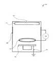
- FIG. 1depicts a plasma processing system 100 for treating substrates using plasma (not shown) that is generated in plasma chamber 102 .
- Plasmamay be generated in the plasma chamber 102 by ionizing gas that is provided by a gas delivery system 104 and exposing the gas to electromagnetic energy provided by a plasma power source 106 .
- a vacuum system 108may also maintain a sub-atmospheric pressure within the plasma chamber 102 during plasma generation.
- Plasma generationmay be done by applying electromagnetic energy to an electrically neutral gas to cause negatively charged electrons to be released from a gas molecule that is positively charged as result of the lost electron. Over time, the electromagnetic energy and the increasing electron collisions within the gas may increase the density of ionized molecules within the gas, such that the ionized molecules may be influenced by potential differences within the plasma chamber 102 . For example, the potential differences within the plasma chamber 102 may direct the ionize molecules towards a substrate (not shown). The ionized molecules 108 may interact with the substrate or treat the substrate in a way that may remove a portion of the substrate or may be deposited unto the substrate. In this way, patterns may be etched into the substrate or films may be deposited onto the substrate.
- Plasma density across the plasma chamber 102may impact the uniformity of the plasma treatment of the substrate.
- the plasma densitymay be ion molecule 108 density within a volume within the plasma chamber 102 .
- Plasma processing uniformitymay be impacted when the plasma density varies across the substrate such that higher plasma density at the center of the substrate may cause a higher etch rate than the etch rate at the edge of the substrate.
- this process non-uniformitymay be the result of ion loss to the chamber wall 110 , specifically for wide gap between plasma source and substrate.
- One approach to resolve the non-uniformitymay be to alter or generate a sheath or boundary potential (not shown) at the chamber wall 110 .
- a detailed view 112illustrates one embodiment of this approach in the plasma chamber 102 .
- the sheath or boundary potentialmay be altered by using a ring electrode assembly comprising a first ring electrode 114 and the second ring electrode 116 disposed between the plasma source electrode 118 and the substrate holder 120 that may be coupled to ground 122 .
- the plasma source electrode 118may include, but is not limited to, inductive coupling sources, microwave sources, radio frequency sources, hallow cathode plasma, alternating or direct current sources, or a combination thereof.
- the ring assemblymay also include a boundary potential source 124 that may be used to influence the boundary potential (not shown) along the chamber wall 110 .
- the boundary potentialwill be discussed in greater detail in the description of FIG. 3 .
- the boundary potentialmay generate a sheath voltage that attracts electrons 126 to a region proximate to the chamber wall 110 .
- This boundary potential formed by electrons 126may be used to push or repel ions 108 away from the chamber wall 110 and may improve the plasma density uniformity across the substrate holder 120 . The improvement in uniformity may be due to reducing the rate of ion 108 loss to the chamber wall 110 .
- the ion 108 density proximate to the edge of the substrate holder 120may be higher than without using the ring electrode assembly.
- the second ring electrode 116may be located adjacent to the substrate holder 122 during plasma processing. The positioning of the second ring electrode 116 is not intended to be limited to the embodiment shown in or described in the description of FIG. 1 .
- FIG. 2is another illustration 200 of a cross section of another embodiment of the ring electrode assembly that may be incorporated into the plasma chamber 102 .
- the layout of the chambermay be impacted by gas flow considerations, in addition to the plasma generation considerations. Hence, being able to reduce the amount of obstructions for gas flow in the plasma chamber 102 may be desirable.
- the components of the plasma chamber 102may be placed or designed to limit interference with gas flow.
- the first ring electrode 114may be incorporated into the chamber wall 110 to minimize the obstruction of gas or plasma flow within the plasma chamber 102 .
- the wall electrode 202may be electrically isolated from the remainder of the chamber wall 110 . This configuration may enable the application of a potential to the wall electrode 202 by the boundary power source 124 without charging non-wall electrode portions of the chamber wall 110 .
- the wall electrode 202may operate in a similar manner as the first ring electrode 114 as described in the description of FIG. 1 . In that the wall electrode 202 , in conjunction with the second electrode 116 , may induce a negative sheath potential proximate to the chamber wall 110 .
- the formation of the sheath or boundary potential layer (not shown) along the chamber wall 110may be the result of a thin region of electric fields (not shown) between the chamber wall 110 and the bulk plasma potential (not shown).
- the potential drop across thin regionis relatively sharp compared to the distribution of the bulk potential voltage; this will be shown and described in the description of FIGS. 3A-3D .
- the change of the potential profile in the plasma chamber 102can be varied by using different power sources powering the ring at different locations.
- the varying power to the first electrode 114 or 202 , pressure, and other plasma conditionscan result in varying potential profiles due to secondary electron emission emitted from the first electrode 114 or 202 and/or the second electrode 116 .
- the potential difference between boundary sheath potential and bulk plasma potentialmay be adjusted so that the potential profiles illustrated in FIGS. 3A-3D .
- a potential profile similar to FIG. 3Cmay form, in which a localized high potential is formed in between bulk plasma potential and the boundary sheath potential.
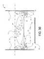
- FIG. 3Ais an illustration 300 of a cross section of the plasma chamber 102 with a plasma potential profile 302 that may be enabled by the ring electrode assembly of FIG. 1 or FIG. 2 .
- the plasma potential profile 302may be inverted during plasma processing without the ring electrode assembly to form a positive plasma potential profile (not shown).
- the illustrated plasma potential profile 302may be referred to as a negative plasma potential profile 302 , in that the potential of the bulk plasma region 304 may have a greater negative potential than the potential at or near the chamber wall 110 .
- the sheath potentialbeing measured from a voltage reference line 310 that may represent the potential reference value for the chamber wall 110 and the potential at the bulk plasma region 304 .
- the negative bulk plasma potentialmay be enabled by the boundary power supply 124 by applying a negative voltage to the first ring electrode 114 and connecting the second ring electrode 116 to the ground of the boundary power supply 124 .
- the potential from the ring electrode assemblye.g., first ring electrode 114 , second ring electrode 116 , etc.
- the potential from the ring electrode assemblymay assist in generating the negative bulk potential region 304 and the boundary sheath region 306 by attracting electrons 126 to the chamber wall 110 .
- At least a majority of the ions 108 adjacent to the sheath regions 306may be repelled or pushed away from the boundary sheath regions 306 .
- an electric pressure forcemay be emitted from the chamber wall 110 towards the bulk plasma region 304 that may prevent the ions 108 from being lost from the bulk plasma region 304 to the chamber wall 110 .
- the repelling or electric pressureis illustrated by the two arrows pointing from the chamber wall 110 towards the bulk potential region 304 .
- the rate of ion 108 loss to the chamber wall 110may be reduced, but may not be completely eliminated by the boundary sheath regions 306 .
- the lower rate of ion 108 lossmay increase the ion density in a region proximate to the chamber wall 110 and may result in a higher number of ions 108 that may be used to treat the edges of the substrate.
- the boundary sheath regions 306may be relatively thin compared to the bulk potential region 304 .
- the bulk potential region 304may be used to treat semiconductor substrates for etching, deposition, ion implant, and the like.
- the semiconductor substratemay be circular and have a diameter of at least 200 mm. Accordingly, the boundary sheath region 306 thickness may be substantially smaller than the substrate diameter by at least two orders of magnitude.
- the horizontal thickness of the boundary sheath region 306may be based on the plasma process conditions which may vary based, at least in part, on electron density, ion temperature (Ti), and electron temperature (Te). The horizontal thickness may be measured from the chamber wall 110 to a horizontal distance away from the chamber wall where the plasma potential profile relatively constant compared to the change in potential proximate to the chamber wall 110 .
- FIG. 3Bis an illustration 312 of a cross section of the plasma chamber with a negative dip plasma potential profile 314 in the plasma chamber 102 that may be enabled by the ring electrode assembly.
- the negative dip plasma potential profile 314may include a secondary boundary region 316 that may include electrons that are isolated from the boundary sheath region 306 by a potential dip 318 in the negative dip plasma potential profile 314 .
- FIG. 3Cis an illustration 320 of a cross section of the plasma chamber 102 with a negative double layer plasma potential profile 322 in the plasma chamber that may be enabled by the ring electrode assembly.
- the negative double layer plasma potential profile 322may include a potential dip 324 similar to the potential dip 318 in FIG. 3B , but the location of the potential dip 324 may offset from the chamber wall 110 by a potential gap distance 326 .
- the potential gap distance 326may enable the ions 308 to be at a higher density and further away from the chamber wall 110 than shown in the FIGS. 3A-3B embodiments.
- FIG. 3Dis an illustration 328 of a cross section of the plasma chamber with a negative-positive double sheath plasma potential profile 330 in the plasma chamber 102 that may be enabled by the ring electrode assembly.
- the negative double sheath plasma potential profile 330may have a bulk potential region 332 that has a positive potential compared to the boundary sheath region 306 . This is in contrast to the bulk potential regions 304 in FIGS. 3A-3C .
- the negative-positive double sheath plasma potential profile 330may also include a potential dip 334 that enables a lower secondary boundary layer 336 to form between the boundary sheath region 306 and the bulk potential region 332 , as shown in FIG. 3D .
- FIG. 4is a flow diagram 400 for a method for implementing a boundary potential profile in the plasma chamber 102 using the ring electrode assembly to minimize ion 108 loss from the bulk plasma region 304 to the chamber wall 110 .
- the first ring electrode 114 or 202 and the second ring electrode 116may be used in conjunction with the boundary power supply 124 to generate a boundary sheath potential region 306 along the chamber wall 110 that prevents at least a majority of the ions 108 from reaching the chamber wall 110 .
- the plasma chamber 102may receive a substrate that may be placed onto a substrate holder that is disposed within the plasma chamber 102 .
- the plasma chamber 102may be enclosed by at least one chamber wall 110 .
- the plasma chamber 102may also include a plasma source 118 configured to generate plasma using one or more gases that may be provided to the plasma chamber 102 via a gas delivery system 104 .
- the vacuum system 108may also be used to vary the pressure within the plasma chamber 102 and evacuate gas or particulates generated during substrate treatment.
- the plasma source 118may receive power from the plasma power source 106 and plasma may be formed inside the plasma chamber 102 .
- the plasmamay include several regions that may include different plasma density characteristics.
- One way to illustrate the plasma characteristicsmay be a region comprising a plasma potential profile 302 that may include a bulk plasma region 304 and the boundary sheath region 306 .
- the bulk plasma region 304may be proximate to the interior region of the plasma chamber 102 and the boundary sheath region 306 disposed between the chamber wall 110 and the bulk plasma region 304 .
- the plasma potential profilee.g., positive potential profile, see FIG. 5
- the plasma densitywill be higher near the center of the plasma chamber than the periphery of the plasma chamber 102 . This may lead to non-uniform processing of the substrate, whether the process is etching, depositing, implanting, or combination thereof.
- One approach to minimize ion 108 loss to the chamber wall 110may be to invert the positive plasma potential profile to form a negative plasma potential profile, as shown in FIG. 3 .
- the negative plasma potential profilemay form a sheath boundary region by attracting electrons in a way that repels or pushes ions 108 away from the chamber wall 110 .
- the plasma chamber 102may include a first electrode 114 or 202 and a second electrode 116 that are coupled to a potential source 124 .
- the potential source 124may apply a potential to an electrode assembly that incorporates the first electrode 114 or 202 and the second electrode 116 to generate the negative plasma potential profile shown in FIG. 3 .
- the applying of the potentialcomprises forming a negative electron sheath (e.g., boundary sheath region 306 ) proximate to the chamber wall 110 , the negative electron sheath comprising a positive potential region (e.g., boundary sheath region 306 ) proximate to the chamber wall 110 that may be at a higher potential than the bulk potential region 304 .
- the first ring electrode 114may be adjacent to or incorporated into the chamber wall 110 to alter the rate of loss of ions from the plasma region (e.g., bulk plasma region 304 ).
- the location of the first ring electrode 114may be between the plasma source 118 and the substrate holder 120 .
- the second ring electrode 116may be disposed below the first ring electrode 114 and above or adjacent to the substrate holder 120 .
- the second ring electrode 116comprises a focus ring surrounding the substrate holder 120 .
- the focus ringmay be designed to control the flow of plasma near the edge of the substrate and/or a portion of the backside of the substrate that may also be exposed to the plasma when positioned in the substrate holder 120 .
- the second ring electrode 116may be coupled to the ground terminal of the boundary power supply 124 .
- the first ring electrode 114 or 202may be coupled to a power output terminal of the boundary power supply 124 .
- the boundary power source 124 that may be coupled to the first ring electrode 114 or 202 and the second ring electrode 116may be of a variety of power sources.
- the ring electrode materialsmay include, but are not limited to, quartz, silicon, ceramic, metal coated with ceramic, and/or carbon based materials.
- One purpose of the boundary power source 124may be to impart a positive charge to the ring electrode assembly to attract electrons from the plasma.
- the boundary power source 124may include, but is not limited to, a continuous wave or a pulsed DC power source, an alternating current (AC) or a low-frequency radio frequency (RF) power from an RF power supply having a first terminal connected to the first ring electrode 114 or 202 and a second terminal connected to the second ring electrode 114 .
- the potential provided by the boundary power supplymay be between 250V and 500V.
- the potentialmay be at least 200V or less than 500V.
- the potentialmay be more than 500V or less than 200V.
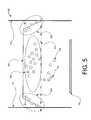
- FIG. 5is an illustration of a cross section 500 of the plasma chamber 102 with a positive plasma potential profile 502 that may be enabled when the ring assembly in FIG. 1 or FIG. 2 may not be used.
- the potential reference line 310may be used as a reference to quantify the plasma potential across the plasma chamber 102 .
- the positive potential profile 502represents the potential of the positive bulk plasma region 504 that may be generated by one or more plasma sources 118 in or coupled to the plasma chamber 102 . Although the regions of the positive potential profile 502 are shown as linear, in other embodiments, the plasma potential profile may also include non-linear regions to reflect non-linear conditions within the plasma.
- the loss of ions 108 to the chamber wall 110causes a lower plasma density proximate to the edge of the substrate 120 .
- the loss of ions 108being indicated by the arrows that indicate the ions 108 leaving the positive bulk plasma region 504 and travelling towards the chamber wall 110 .
- the loss of ions to the chamber wall 110may result in non-uniform process conditions across the substrate, particularly from the center of the substrate 120 to the edge of the substrate 120 .
- biasing the ring assembly in FIG. 1 or 2may alter the positive plasma potential profile 504 to become a negative plasma potential profile 302 .
- the ion 108 wall lossmay be minimized by the formation of the sheath boundary region 306 that may repel or push ions 108 away from the wall.
Landscapes
- Engineering & Computer Science (AREA)
- Physics & Mathematics (AREA)
- Plasma & Fusion (AREA)
- Chemical & Material Sciences (AREA)
- Analytical Chemistry (AREA)
- General Physics & Mathematics (AREA)
- Condensed Matter Physics & Semiconductors (AREA)
- Manufacturing & Machinery (AREA)
- Computer Hardware Design (AREA)
- Microelectronics & Electronic Packaging (AREA)
- Power Engineering (AREA)
- Chemical Vapour Deposition (AREA)
- Plasma Technology (AREA)
- Drying Of Semiconductors (AREA)
Abstract
Description
- This application claims the benefit of and priority to prior filed co-pending U.S. application Ser. No. 14/206,518 filed Mar. 12, 2014 and Provisional Application Ser. No. 61/794,073 filed Mar. 15, 2013, the entire contents of which are expressly incorporated herein by reference.
- This invention relates to semiconductor processing technology, and more particularly, to apparatus and methods for controlling plasma properties of a processing system for treating a substrate.
- Plasma uniformity control during plasma processing for treating semiconductor substrates is important to achieve patterning structures on a substrate or controlling the amount of material removed from or deposited on or into the substrate. A plasma processing system may include a large distance or gap between the plasma source and the substrate. A chamber wall of the plasma processing may be disposed between the plasma source and the substrate. As a result, ions and electrons in the plasma may be influenced by the potential difference between the plasma and the chamber wall. The ions proximate to the chamber wall may migrate towards the chamber wall instead of the substrate. The loss of ions to the chamber wall may alter the plasma density profile across the substrate that may introduce processing non-uniformities that may negatively impact semiconductor devices being built in or on the substrate. For example, a lower plasma density at the edge of the substrate may induce a lower etch or deposition rate at the edge of the substrate than at the center of the substrate. Hence, systems and methods that improve plasma density profile uniformity may be desirable.
- This disclosure relates to a plasma processing system for controlling plasma density near the edge or perimeter of a substrate that is being processed. The plasma processing system may include a plasma chamber that can receive and process the substrate using plasma for etching the substrate, doping the substrate, or depositing a film on the substrate.
- The plasma chamber may include one or more plasma sources that can emit electromagnetic energy to ionize gas that is delivered via a gas delivery system. The distance between the plasma and the substrate may sufficiently confine the charted particles in the plasma to enable a uniform plasma density. The charged particles may be attracted to chamber wall that prevent charged particles from reaching the substrate, particular at substrate edge region. The loss of the charge particles to such as boundary or chamber wall may result in plasma density non-uniformity that leads to substrate processing non-uniformity.
- One approach to minimizing charged particle (e.g., ions) loss may be to alter the boundary potential at the chamber wall in a way that may push the charged particles away from the chamber wall. In other words, building a potential difference proximate to the chamber wall may generate an electric pressure that prevents most charged particles from being lost to the chamber wall. The electric pressure pushes the ions away from the chamber wall. The boundary potential may be altered by including two ring electrodes, or their equivalents, that may be disposed between the plasma source(s) and the substrate. The two ring electrodes may be coupled together via a power source (e.g., direct current, radio frequency, etc.). The boundary potential or plasma sheath at the chamber wall may be altered by this arrangement in way that generates a sheath conditions that enable the electric pressure concept described above.
- The multi-ring assembly design may be used with other plasma sources in a plasma processing chamber to reduce plasma density non-uniformity. The plasma source(s) may include, but is not limited to, inductive coupling sources, microwave sources, radio frequency sources, or a combination thereof.
- The accompanying drawings, which are incorporated in and constitute a part of this specification, illustrate embodiments of the invention and, together with a general description of the invention given above, and the detailed description given below, serve to explain the invention. Additionally, the left most digit(s) of a reference number identifies the drawing in which the reference number first appears.
FIG. 1 is an illustration of a representative embodiment of a plasma processing system that shows a schematic cross-sectional illustration of a plasma chamber that includes a perspective view of a ring electrode assembly.FIG. 2 is another illustration of a cross section a plasma chamber that incorporates the chamber wall in to the ring electrode assembly.FIG. 3A is an illustration of a cross section of the plasma chamber with a plasma potential profile in the plasma chamber that may be enabled by the ring electrode assembly.FIG. 3B is an illustration of a cross section of the plasma chamber with a plasma potential profile in the plasma chamber that may be enabled by the ring electrode assembly.FIG. 3C is an illustration of a cross section of the plasma chamber with a plasma potential profile in the plasma chamber that may be enabled by the ring electrode assembly.FIG. 3D is an illustration of a cross section of the plasma chamber with a plasma potential profile in the plasma chamber that may be enabled by the ring electrode assembly.FIG. 4 is a flow diagram for a method for implementing a boundary potential profile in the plasma chamber that minimizes ion loss from the plasma to the chamber wall.FIG. 5 is an illustration of a cross section of the plasma chamber with a positive plasma potential profile in the plasma chamber.- The following Detailed Description refers to accompanying drawings to illustrate exemplary embodiments consistent with the present disclosure. References in the Detailed Description to “one embodiment,” “an embodiment,” “an exemplary embodiment,” etc., indicate that the exemplary embodiment described can include a particular feature, structure, or characteristic, but every exemplary embodiment does not necessarily include the particular feature, structure, or characteristic. Moreover, such phrases are not necessarily referring to the same embodiment. Further, when a particular feature, structure, or characteristic is described in connection with an embodiment, it is within the knowledge of those skilled in the relevant art(s) to affect such feature, structure, or characteristic in connection with other exemplary embodiments whether or not explicitly described.
- The exemplary embodiments described herein are provided for illustrative purposes, and are not limiting. Other embodiments are possible, and modifications can be made to exemplary embodiments within the scope of the present disclosure. Therefore, the Detailed Description is not meant to limit the present disclosure. Rather, the scope of the present disclosure is defined only in accordance with the following claims and their equivalents.
- The following Detailed Description of the exemplary embodiments will so fully reveal the general nature of the present disclosure that others can, by applying knowledge of those skilled in the relevant art(s), readily modify and/or adapt for various applications such exemplary embodiments, without undue experimentation, without departing from the scope of the present disclosure. Therefore, such adaptations and modifications are intended to be within the meaning and plurality of equivalents of the exemplary embodiments based upon the teaching and guidance presented herein. It is to be understood that the phraseology or terminology herein is for the purpose of description and not limitation, such that the terminology or phraseology of the present specification is to be interpreted by those skilled in relevant art(s) in light of the teachings herein.
FIG. 1 depicts aplasma processing system 100 for treating substrates using plasma (not shown) that is generated inplasma chamber 102. Plasma may be generated in theplasma chamber 102 by ionizing gas that is provided by agas delivery system 104 and exposing the gas to electromagnetic energy provided by aplasma power source 106. Avacuum system 108 may also maintain a sub-atmospheric pressure within theplasma chamber 102 during plasma generation.- Plasma generation may be done by applying electromagnetic energy to an electrically neutral gas to cause negatively charged electrons to be released from a gas molecule that is positively charged as result of the lost electron. Over time, the electromagnetic energy and the increasing electron collisions within the gas may increase the density of ionized molecules within the gas, such that the ionized molecules may be influenced by potential differences within the
plasma chamber 102. For example, the potential differences within theplasma chamber 102 may direct the ionize molecules towards a substrate (not shown). Theionized molecules 108 may interact with the substrate or treat the substrate in a way that may remove a portion of the substrate or may be deposited unto the substrate. In this way, patterns may be etched into the substrate or films may be deposited onto the substrate. - Plasma density across the
plasma chamber 102 may impact the uniformity of the plasma treatment of the substrate. The plasma density may beion molecule 108 density within a volume within theplasma chamber 102. Plasma processing uniformity may be impacted when the plasma density varies across the substrate such that higher plasma density at the center of the substrate may cause a higher etch rate than the etch rate at the edge of the substrate. Generally, this process non-uniformity may be the result of ion loss to thechamber wall 110, specifically for wide gap between plasma source and substrate. One approach to resolve the non-uniformity may be to alter or generate a sheath or boundary potential (not shown) at thechamber wall 110. Adetailed view 112 illustrates one embodiment of this approach in theplasma chamber 102. - In one embodiment, the sheath or boundary potential may be altered by using a ring electrode assembly comprising a
first ring electrode 114 and thesecond ring electrode 116 disposed between theplasma source electrode 118 and thesubstrate holder 120 that may be coupled toground 122. Theplasma source electrode 118 may include, but is not limited to, inductive coupling sources, microwave sources, radio frequency sources, hallow cathode plasma, alternating or direct current sources, or a combination thereof. - The ring assembly may also include a boundary
potential source 124 that may be used to influence the boundary potential (not shown) along thechamber wall 110. The boundary potential will be discussed in greater detail in the description ofFIG. 3 . In short, the boundary potential may generate a sheath voltage that attractselectrons 126 to a region proximate to thechamber wall 110. This boundary potential formed byelectrons 126 may be used to push or repelions 108 away from thechamber wall 110 and may improve the plasma density uniformity across thesubstrate holder 120. The improvement in uniformity may be due to reducing the rate ofion 108 loss to thechamber wall 110. In this way, theion 108 density proximate to the edge of thesubstrate holder 120 may be higher than without using the ring electrode assembly. In another embodiment, thesecond ring electrode 116 may be located adjacent to thesubstrate holder 122 during plasma processing. The positioning of thesecond ring electrode 116 is not intended to be limited to the embodiment shown in or described in the description ofFIG. 1 . FIG. 2 is anotherillustration 200 of a cross section of another embodiment of the ring electrode assembly that may be incorporated into theplasma chamber 102. In plasma processing systems, the layout of the chamber may be impacted by gas flow considerations, in addition to the plasma generation considerations. Hence, being able to reduce the amount of obstructions for gas flow in theplasma chamber 102 may be desirable. The components of theplasma chamber 102 may be placed or designed to limit interference with gas flow.- In the
FIG. 2 embodiment, thefirst ring electrode 114 may be incorporated into thechamber wall 110 to minimize the obstruction of gas or plasma flow within theplasma chamber 102. Thewall electrode 202 may be electrically isolated from the remainder of thechamber wall 110. This configuration may enable the application of a potential to thewall electrode 202 by theboundary power source 124 without charging non-wall electrode portions of thechamber wall 110. Thewall electrode 202 may operate in a similar manner as thefirst ring electrode 114 as described in the description ofFIG. 1 . In that thewall electrode 202, in conjunction with thesecond electrode 116, may induce a negative sheath potential proximate to thechamber wall 110. - The formation of the sheath or boundary potential layer (not shown) along the
chamber wall 110 may be the result of a thin region of electric fields (not shown) between thechamber wall 110 and the bulk plasma potential (not shown). The potential drop across thin region is relatively sharp compared to the distribution of the bulk potential voltage; this will be shown and described in the description ofFIGS. 3A-3D . - In
FIGS. 3A-3D , the change of the potential profile in theplasma chamber 102 can be varied by using different power sources powering the ring at different locations. The varying power to thefirst electrode first electrode second electrode 116. The potential difference between boundary sheath potential and bulk plasma potential may be adjusted so that the potential profiles illustrated inFIGS. 3A-3D . In another embodiment, if a localized field or secondary localized plasma potential from a localized plasma source was formed by a ring structure similar to thefirst electrode 114 adjacent to the wall, a potential profile similar toFIG. 3C may form, in which a localized high potential is formed in between bulk plasma potential and the boundary sheath potential. FIG. 3A is anillustration 300 of a cross section of theplasma chamber 102 with a plasmapotential profile 302 that may be enabled by the ring electrode assembly ofFIG. 1 orFIG. 2 . Generally, the plasmapotential profile 302 may be inverted during plasma processing without the ring electrode assembly to form a positive plasma potential profile (not shown). The illustrated plasmapotential profile 302 may be referred to as a negative plasmapotential profile 302, in that the potential of thebulk plasma region 304 may have a greater negative potential than the potential at or near thechamber wall 110. The sheath potential being measured from avoltage reference line 310 that may represent the potential reference value for thechamber wall 110 and the potential at thebulk plasma region 304.- The negative bulk plasma potential may be enabled by the
boundary power supply 124 by applying a negative voltage to thefirst ring electrode 114 and connecting thesecond ring electrode 116 to the ground of theboundary power supply 124. The potential from the ring electrode assembly (e.g.,first ring electrode 114,second ring electrode 116, etc.) may assist in generating the negative bulkpotential region 304 and theboundary sheath region 306 by attractingelectrons 126 to thechamber wall 110. At least a majority of theions 108 adjacent to thesheath regions 306 may be repelled or pushed away from theboundary sheath regions 306. In other words, an electric pressure force may be emitted from thechamber wall 110 towards thebulk plasma region 304 that may prevent theions 108 from being lost from thebulk plasma region 304 to thechamber wall 110. The repelling or electric pressure is illustrated by the two arrows pointing from thechamber wall 110 towards the bulkpotential region 304. The rate ofion 108 loss to thechamber wall 110 may be reduced, but may not be completely eliminated by theboundary sheath regions 306. The lower rate ofion 108 loss may increase the ion density in a region proximate to thechamber wall 110 and may result in a higher number ofions 108 that may be used to treat the edges of the substrate. - In one embodiment, the
boundary sheath regions 306 may be relatively thin compared to the bulkpotential region 304. The bulkpotential region 304 may be used to treat semiconductor substrates for etching, deposition, ion implant, and the like. In one specific embodiment, the semiconductor substrate may be circular and have a diameter of at least 200 mm. Accordingly, theboundary sheath region 306 thickness may be substantially smaller than the substrate diameter by at least two orders of magnitude. The horizontal thickness of theboundary sheath region 306 may be based on the plasma process conditions which may vary based, at least in part, on electron density, ion temperature (Ti), and electron temperature (Te). The horizontal thickness may be measured from thechamber wall 110 to a horizontal distance away from the chamber wall where the plasma potential profile relatively constant compared to the change in potential proximate to thechamber wall 110. FIG. 3B is anillustration 312 of a cross section of the plasma chamber with a negative dip plasmapotential profile 314 in theplasma chamber 102 that may be enabled by the ring electrode assembly. The negative dip plasmapotential profile 314 may include asecondary boundary region 316 that may include electrons that are isolated from theboundary sheath region 306 by apotential dip 318 in the negative dip plasmapotential profile 314.FIG. 3C is anillustration 320 of a cross section of theplasma chamber 102 with a negative double layer plasmapotential profile 322 in the plasma chamber that may be enabled by the ring electrode assembly. The negative double layer plasmapotential profile 322 may include apotential dip 324 similar to thepotential dip 318 inFIG. 3B , but the location of thepotential dip 324 may offset from thechamber wall 110 by apotential gap distance 326. In short, thepotential gap distance 326 may enable theions 308 to be at a higher density and further away from thechamber wall 110 than shown in theFIGS. 3A-3B embodiments.FIG. 3D is anillustration 328 of a cross section of the plasma chamber with a negative-positive double sheath plasmapotential profile 330 in theplasma chamber 102 that may be enabled by the ring electrode assembly. The negative double sheath plasmapotential profile 330 may have a bulkpotential region 332 that has a positive potential compared to theboundary sheath region 306. This is in contrast to the bulkpotential regions 304 inFIGS. 3A-3C . The negative-positive double sheath plasmapotential profile 330 may also include apotential dip 334 that enables a lowersecondary boundary layer 336 to form between theboundary sheath region 306 and the bulkpotential region 332, as shown inFIG. 3D .FIG. 4 is a flow diagram400 for a method for implementing a boundary potential profile in theplasma chamber 102 using the ring electrode assembly to minimizeion 108 loss from thebulk plasma region 304 to thechamber wall 110. Thefirst ring electrode second ring electrode 116 may be used in conjunction with theboundary power supply 124 to generate a boundary sheathpotential region 306 along thechamber wall 110 that prevents at least a majority of theions 108 from reaching thechamber wall 110.- At
block 402, theplasma chamber 102 may receive a substrate that may be placed onto a substrate holder that is disposed within theplasma chamber 102. Theplasma chamber 102 may be enclosed by at least onechamber wall 110. To generate plasma, theplasma chamber 102 may also include aplasma source 118 configured to generate plasma using one or more gases that may be provided to theplasma chamber 102 via agas delivery system 104. Thevacuum system 108 may also be used to vary the pressure within theplasma chamber 102 and evacuate gas or particulates generated during substrate treatment. - At
block 404, theplasma source 118 may receive power from theplasma power source 106 and plasma may be formed inside theplasma chamber 102. The plasma may include several regions that may include different plasma density characteristics. One way to illustrate the plasma characteristics may be a region comprising a plasmapotential profile 302 that may include abulk plasma region 304 and theboundary sheath region 306. Thebulk plasma region 304 may be proximate to the interior region of theplasma chamber 102 and theboundary sheath region 306 disposed between thechamber wall 110 and thebulk plasma region 304. However, the plasma potential profile (e.g., positive potential profile, seeFIG. 5 ) may induceion 108 loss to thechamber wall 110. Accordingly, the plasma density will be higher near the center of the plasma chamber than the periphery of theplasma chamber 102. This may lead to non-uniform processing of the substrate, whether the process is etching, depositing, implanting, or combination thereof. - One approach to minimize
ion 108 loss to thechamber wall 110 may be to invert the positive plasma potential profile to form a negative plasma potential profile, as shown inFIG. 3 . The negative plasma potential profile may form a sheath boundary region by attracting electrons in a way that repels or pushesions 108 away from thechamber wall 110. In one embodiment, theplasma chamber 102 may include afirst electrode second electrode 116 that are coupled to apotential source 124. - At
block 406, thepotential source 124 may apply a potential to an electrode assembly that incorporates thefirst electrode second electrode 116 to generate the negative plasma potential profile shown inFIG. 3 . The applying of the potential comprises forming a negative electron sheath (e.g., boundary sheath region306) proximate to thechamber wall 110, the negative electron sheath comprising a positive potential region (e.g., boundary sheath region306) proximate to thechamber wall 110 that may be at a higher potential than the bulkpotential region 304. - In one embodiment, the
first ring electrode 114 may be adjacent to or incorporated into thechamber wall 110 to alter the rate of loss of ions from the plasma region (e.g., bulk plasma region304). The location of thefirst ring electrode 114 may be between theplasma source 118 and thesubstrate holder 120. Thesecond ring electrode 116 may be disposed below thefirst ring electrode 114 and above or adjacent to thesubstrate holder 120. In one specific embodiment, thesecond ring electrode 116 comprises a focus ring surrounding thesubstrate holder 120. The focus ring may be designed to control the flow of plasma near the edge of the substrate and/or a portion of the backside of the substrate that may also be exposed to the plasma when positioned in thesubstrate holder 120. Thesecond ring electrode 116 may be coupled to the ground terminal of theboundary power supply 124. Thefirst ring electrode boundary power supply 124. - The
boundary power source 124 that may be coupled to thefirst ring electrode second ring electrode 116 may be of a variety of power sources. The ring electrode materials may include, but are not limited to, quartz, silicon, ceramic, metal coated with ceramic, and/or carbon based materials. One purpose of theboundary power source 124 may be to impart a positive charge to the ring electrode assembly to attract electrons from the plasma. Theboundary power source 124 may include, but is not limited to, a continuous wave or a pulsed DC power source, an alternating current (AC) or a low-frequency radio frequency (RF) power from an RF power supply having a first terminal connected to thefirst ring electrode second ring electrode 114. In one embodiment, the potential provided by the boundary power supply may be between 250V and 500V. In another embodiment, the potential may be at least 200V or less than 500V. In another embodiment, the potential may be more than 500V or less than 200V. FIG. 5 is an illustration of across section 500 of theplasma chamber 102 with a positive plasmapotential profile 502 that may be enabled when the ring assembly inFIG. 1 orFIG. 2 may not be used. Thepotential reference line 310 may be used as a reference to quantify the plasma potential across theplasma chamber 102. The positivepotential profile 502 represents the potential of the positivebulk plasma region 504 that may be generated by one ormore plasma sources 118 in or coupled to theplasma chamber 102. Although the regions of the positivepotential profile 502 are shown as linear, in other embodiments, the plasma potential profile may also include non-linear regions to reflect non-linear conditions within the plasma.- One concern with the positive
bulk plasma region 504 is due to the attraction of the relatively higherpotential ions 108 to thechamber wall 110 that may be at a lower potential than theions 108. Accordingly, the loss ofions 108 to thechamber wall 110 causes a lower plasma density proximate to the edge of thesubstrate 120. The loss ofions 108 being indicated by the arrows that indicate theions 108 leaving the positivebulk plasma region 504 and travelling towards thechamber wall 110. The loss of ions to thechamber wall 110 may result in non-uniform process conditions across the substrate, particularly from the center of thesubstrate 120 to the edge of thesubstrate 120. As noted above in the description ofFIG. 3 , biasing the ring assembly inFIG. 1 or2 may alter the positive plasmapotential profile 504 to become a negative plasmapotential profile 302. Theion 108 wall loss may be minimized by the formation of thesheath boundary region 306 that may repel or pushions 108 away from the wall. - It is to be appreciated that the Detailed Description section, and not the Abstract section, is intended to be used to interpret the claims. The Abstract section can set forth one or more, but not all exemplary embodiments, of the present disclosure, and thus, is not intended to limit the present disclosure and the appended claims in any way.
- While the present disclosure has been illustrated by the description of one or more embodiments thereof, and while the embodiments have been described in considerable detail, they are not intended to restrict or in any way limit the scope of the appended claims to such detail. Additional advantages and modifications will readily appear to those skilled in art. The invention in its broader aspects is therefore not limited to the specific details, representative apparatus and method and illustrative examples shown and described. Accordingly, departures may be made from such details without departing from the scope of the general inventive concept.
Claims (8)
Priority Applications (1)
| Application Number | Priority Date | Filing Date | Title |
|---|---|---|---|
| US14/932,057US11728135B2 (en) | 2013-03-15 | 2015-11-04 | Electric pressure systems for control of plasma properties and uniformity |
Applications Claiming Priority (3)
| Application Number | Priority Date | Filing Date | Title |
|---|---|---|---|
| US201361794073P | 2013-03-15 | 2013-03-15 | |
| US14/206,518US9209032B2 (en) | 2013-03-15 | 2014-03-12 | Electric pressure systems for control of plasma properties and uniformity |
| US14/932,057US11728135B2 (en) | 2013-03-15 | 2015-11-04 | Electric pressure systems for control of plasma properties and uniformity |
Related Parent Applications (1)
| Application Number | Title | Priority Date | Filing Date |
|---|---|---|---|
| US14/206,518DivisionUS9209032B2 (en) | 2013-03-15 | 2014-03-12 | Electric pressure systems for control of plasma properties and uniformity |
Publications (2)
| Publication Number | Publication Date |
|---|---|
| US20160056018A1true US20160056018A1 (en) | 2016-02-25 |
| US11728135B2 US11728135B2 (en) | 2023-08-15 |
Family
ID=51528993
Family Applications (2)
| Application Number | Title | Priority Date | Filing Date |
|---|---|---|---|
| US14/206,518Expired - Fee RelatedUS9209032B2 (en) | 2013-03-15 | 2014-03-12 | Electric pressure systems for control of plasma properties and uniformity |
| US14/932,057Active2035-05-14US11728135B2 (en) | 2013-03-15 | 2015-11-04 | Electric pressure systems for control of plasma properties and uniformity |
Family Applications Before (1)
| Application Number | Title | Priority Date | Filing Date |
|---|---|---|---|
| US14/206,518Expired - Fee RelatedUS9209032B2 (en) | 2013-03-15 | 2014-03-12 | Electric pressure systems for control of plasma properties and uniformity |
Country Status (1)
| Country | Link |
|---|---|
| US (2) | US9209032B2 (en) |
Cited By (1)
| Publication number | Priority date | Publication date | Assignee | Title |
|---|---|---|---|---|
| US20200402810A1 (en)* | 2018-02-13 | 2020-12-24 | Korea Basic Science Institute | Point etching module using annular surface dielectric barrier discharge apparatus and method for control etching profile of point etching module |
Families Citing this family (28)
| Publication number | Priority date | Publication date | Assignee | Title |
|---|---|---|---|---|
| US10510575B2 (en) | 2017-09-20 | 2019-12-17 | Applied Materials, Inc. | Substrate support with multiple embedded electrodes |
| KR102722787B1 (en)* | 2017-12-04 | 2024-10-25 | 포항공과대학교 산학협력단 | Expansion method for sheath and bulk of microwave plasma induced by Radio Frequency bias |
| US10555412B2 (en) | 2018-05-10 | 2020-02-04 | Applied Materials, Inc. | Method of controlling ion energy distribution using a pulse generator with a current-return output stage |
| US11476145B2 (en) | 2018-11-20 | 2022-10-18 | Applied Materials, Inc. | Automatic ESC bias compensation when using pulsed DC bias |
| KR102827481B1 (en) | 2019-01-22 | 2025-06-30 | 어플라이드 머티어리얼스, 인코포레이티드 | Feedback loop to control pulse voltage waveform |
| US11508554B2 (en) | 2019-01-24 | 2022-11-22 | Applied Materials, Inc. | High voltage filter assembly |
| WO2020185609A1 (en)* | 2019-03-14 | 2020-09-17 | Lam Research Corporation | Plasma etch tool for high aspect ratio etching |
| US11848176B2 (en) | 2020-07-31 | 2023-12-19 | Applied Materials, Inc. | Plasma processing using pulsed-voltage and radio-frequency power |
| US11901157B2 (en) | 2020-11-16 | 2024-02-13 | Applied Materials, Inc. | Apparatus and methods for controlling ion energy distribution |
| US11798790B2 (en) | 2020-11-16 | 2023-10-24 | Applied Materials, Inc. | Apparatus and methods for controlling ion energy distribution |
| US11495470B1 (en) | 2021-04-16 | 2022-11-08 | Applied Materials, Inc. | Method of enhancing etching selectivity using a pulsed plasma |
| US20220349050A1 (en)* | 2021-04-30 | 2022-11-03 | Applied Materials, Inc. | Method and apparatus with high conductance components for chamber cleaning |
| US11791138B2 (en) | 2021-05-12 | 2023-10-17 | Applied Materials, Inc. | Automatic electrostatic chuck bias compensation during plasma processing |
| US11948780B2 (en) | 2021-05-12 | 2024-04-02 | Applied Materials, Inc. | Automatic electrostatic chuck bias compensation during plasma processing |
| US11967483B2 (en) | 2021-06-02 | 2024-04-23 | Applied Materials, Inc. | Plasma excitation with ion energy control |
| US12394596B2 (en) | 2021-06-09 | 2025-08-19 | Applied Materials, Inc. | Plasma uniformity control in pulsed DC plasma chamber |
| US20220399185A1 (en) | 2021-06-09 | 2022-12-15 | Applied Materials, Inc. | Plasma chamber and chamber component cleaning methods |
| US11810760B2 (en) | 2021-06-16 | 2023-11-07 | Applied Materials, Inc. | Apparatus and method of ion current compensation |
| US11569066B2 (en) | 2021-06-23 | 2023-01-31 | Applied Materials, Inc. | Pulsed voltage source for plasma processing applications |
| US11776788B2 (en) | 2021-06-28 | 2023-10-03 | Applied Materials, Inc. | Pulsed voltage boost for substrate processing |
| US11476090B1 (en) | 2021-08-24 | 2022-10-18 | Applied Materials, Inc. | Voltage pulse time-domain multiplexing |
| US12106938B2 (en) | 2021-09-14 | 2024-10-01 | Applied Materials, Inc. | Distortion current mitigation in a radio frequency plasma processing chamber |
| US11694876B2 (en) | 2021-12-08 | 2023-07-04 | Applied Materials, Inc. | Apparatus and method for delivering a plurality of waveform signals during plasma processing |
| US11972924B2 (en) | 2022-06-08 | 2024-04-30 | Applied Materials, Inc. | Pulsed voltage source for plasma processing applications |
| US12315732B2 (en) | 2022-06-10 | 2025-05-27 | Applied Materials, Inc. | Method and apparatus for etching a semiconductor substrate in a plasma etch chamber |
| US12272524B2 (en) | 2022-09-19 | 2025-04-08 | Applied Materials, Inc. | Wideband variable impedance load for high volume manufacturing qualification and on-site diagnostics |
| US12111341B2 (en) | 2022-10-05 | 2024-10-08 | Applied Materials, Inc. | In-situ electric field detection method and apparatus |
| WO2024196889A1 (en)* | 2023-03-18 | 2024-09-26 | Matthew Steele | Plasma generation apparatus, system, and method |
Citations (13)
| Publication number | Priority date | Publication date | Assignee | Title |
|---|---|---|---|---|
| US5531862A (en)* | 1993-07-19 | 1996-07-02 | Hitachi, Ltd. | Method of and apparatus for removing foreign particles |
| US5817534A (en)* | 1995-12-04 | 1998-10-06 | Applied Materials, Inc. | RF plasma reactor with cleaning electrode for cleaning during processing of semiconductor wafers |
| US6124003A (en)* | 1998-04-02 | 2000-09-26 | Nissin Electric Co., Ltd. | Film depositing method and film depositing apparatus |
| US6184489B1 (en)* | 1998-04-13 | 2001-02-06 | Nec Corporation | Particle-removing apparatus for a semiconductor device manufacturing apparatus and method of removing particles |
| US20030168588A1 (en)* | 2002-03-05 | 2003-09-11 | Sumitomo Eaton Nova Corporation | Ion beam mass separation filter, mass separation method thereof and ion source using the same |
| US20050214477A1 (en)* | 2004-03-26 | 2005-09-29 | Applied Materials, Inc. | Chemical vapor deposition plasma process using an ion shower grid |
| US20050260354A1 (en)* | 2004-05-20 | 2005-11-24 | Varian Semiconductor Equipment Associates, Inc. | In-situ process chamber preparation methods for plasma ion implantation systems |
| US20070023398A1 (en)* | 2005-07-27 | 2007-02-01 | Hitachi High-Technologies Corporation | Plasma processing apparatus |
| US20080110747A1 (en)* | 1999-10-08 | 2008-05-15 | Applied Materials, Inc. | Self-ionized and inductively-coupled plasma for sputtering and resputtering |
| US20080142481A1 (en)* | 2006-12-18 | 2008-06-19 | White John M | In-situ particle collector |
| US20080180357A1 (en)* | 2007-01-25 | 2008-07-31 | Kawakami Masatoshi | Plasma processing apparatus |
| US20090242127A1 (en)* | 2008-03-28 | 2009-10-01 | Tokyo Electron Limited | Plasma etching apparatus and method, and computer-readable storage medium |
| US20140273538A1 (en)* | 2013-03-15 | 2014-09-18 | Tokyo Electron Limited | Non-ambipolar electric pressure plasma uniformity control |
Family Cites Families (10)
| Publication number | Priority date | Publication date | Assignee | Title |
|---|---|---|---|---|
| JPS6020440A (en)* | 1983-07-14 | 1985-02-01 | Tokyo Daigaku | Ion beam processing equipment |
| KR880013424A (en)* | 1987-04-08 | 1988-11-30 | 미타 가츠시게 | Plasma device |
| JPH09106899A (en)* | 1995-10-11 | 1997-04-22 | Anelva Corp | Plasma CVD apparatus and method and dry etching apparatus and method |
| US6361661B2 (en)* | 1997-05-16 | 2002-03-26 | Applies Materials, Inc. | Hybrid coil design for ionized deposition |
| JP4340348B2 (en)* | 1998-01-22 | 2009-10-07 | 株式会社日立国際電気 | Plasma generator |
| US6476399B1 (en)* | 2000-09-01 | 2002-11-05 | Axcelis Technologies, Inc. | System and method for removing contaminant particles relative to an ion beam |
| TW511398B (en)* | 2000-09-12 | 2002-11-21 | Tokyo Electron Ltd | Apparatus and method to control the uniformity of plasma by reducing radial loss |
| JP4374487B2 (en)* | 2003-06-06 | 2009-12-02 | 株式会社Sen | Ion source apparatus and cleaning optimization method thereof |
| US7829469B2 (en)* | 2006-12-11 | 2010-11-09 | Tokyo Electron Limited | Method and system for uniformity control in ballistic electron beam enhanced plasma processing system |
| JP5702968B2 (en) | 2010-08-11 | 2015-04-15 | 東京エレクトロン株式会社 | Plasma processing apparatus and plasma control method |
- 2014
- 2014-03-12USUS14/206,518patent/US9209032B2/ennot_activeExpired - Fee Related
- 2015
- 2015-11-04USUS14/932,057patent/US11728135B2/enactiveActive
Patent Citations (13)
| Publication number | Priority date | Publication date | Assignee | Title |
|---|---|---|---|---|
| US5531862A (en)* | 1993-07-19 | 1996-07-02 | Hitachi, Ltd. | Method of and apparatus for removing foreign particles |
| US5817534A (en)* | 1995-12-04 | 1998-10-06 | Applied Materials, Inc. | RF plasma reactor with cleaning electrode for cleaning during processing of semiconductor wafers |
| US6124003A (en)* | 1998-04-02 | 2000-09-26 | Nissin Electric Co., Ltd. | Film depositing method and film depositing apparatus |
| US6184489B1 (en)* | 1998-04-13 | 2001-02-06 | Nec Corporation | Particle-removing apparatus for a semiconductor device manufacturing apparatus and method of removing particles |
| US20080110747A1 (en)* | 1999-10-08 | 2008-05-15 | Applied Materials, Inc. | Self-ionized and inductively-coupled plasma for sputtering and resputtering |
| US20030168588A1 (en)* | 2002-03-05 | 2003-09-11 | Sumitomo Eaton Nova Corporation | Ion beam mass separation filter, mass separation method thereof and ion source using the same |
| US20050214477A1 (en)* | 2004-03-26 | 2005-09-29 | Applied Materials, Inc. | Chemical vapor deposition plasma process using an ion shower grid |
| US20050260354A1 (en)* | 2004-05-20 | 2005-11-24 | Varian Semiconductor Equipment Associates, Inc. | In-situ process chamber preparation methods for plasma ion implantation systems |
| US20070023398A1 (en)* | 2005-07-27 | 2007-02-01 | Hitachi High-Technologies Corporation | Plasma processing apparatus |
| US20080142481A1 (en)* | 2006-12-18 | 2008-06-19 | White John M | In-situ particle collector |
| US20080180357A1 (en)* | 2007-01-25 | 2008-07-31 | Kawakami Masatoshi | Plasma processing apparatus |
| US20090242127A1 (en)* | 2008-03-28 | 2009-10-01 | Tokyo Electron Limited | Plasma etching apparatus and method, and computer-readable storage medium |
| US20140273538A1 (en)* | 2013-03-15 | 2014-09-18 | Tokyo Electron Limited | Non-ambipolar electric pressure plasma uniformity control |
Cited By (2)
| Publication number | Priority date | Publication date | Assignee | Title |
|---|---|---|---|---|
| US20200402810A1 (en)* | 2018-02-13 | 2020-12-24 | Korea Basic Science Institute | Point etching module using annular surface dielectric barrier discharge apparatus and method for control etching profile of point etching module |
| US11776819B2 (en)* | 2018-02-13 | 2023-10-03 | Korea Institute Of Fusion Energy | Point etching module using annular surface dielectric barrier discharge apparatus and method for control etching profile of point etching module |
Also Published As
| Publication number | Publication date |
|---|---|
| US11728135B2 (en) | 2023-08-15 |
| US9209032B2 (en) | 2015-12-08 |
| US20140273485A1 (en) | 2014-09-18 |
Similar Documents
| Publication | Publication Date | Title |
|---|---|---|
| US9209032B2 (en) | Electric pressure systems for control of plasma properties and uniformity | |
| TWI703660B (en) | System and method for controlling plasma density | |
| KR100437956B1 (en) | Method and apparatus for ionized physical vapor deposition | |
| CN111247617B (en) | Linear high-energy radio frequency plasma ion source | |
| US9177756B2 (en) | E-beam enhanced decoupled source for semiconductor processing | |
| US9111728B2 (en) | E-beam enhanced decoupled source for semiconductor processing | |
| US10388528B2 (en) | Non-ambipolar electric pressure plasma uniformity control | |
| US6861643B2 (en) | Neutral particle beam processing apparatus | |
| US20120258607A1 (en) | E-Beam Enhanced Decoupled Source for Semiconductor Processing | |
| US20110272100A1 (en) | Plasma processing apparatus, plasma processing method, focus ring, and focus ring component | |
| US8911602B2 (en) | Dual hexagonal shaped plasma source | |
| US20060121704A1 (en) | Plasma ion implantation system with axial electrostatic confinement | |
| US20180053631A1 (en) | Low Electron Temperature Etch Chamber with Independent Control Over Plasma Density, Radical Composition Ion Energy for Atomic Precision Etching | |
| KR20140024375A (en) | E-beam enhanced decoupled source for semiconductor processing | |
| CN104900470A (en) | Plasma-based material modification using a plasma source with magnetic confinement | |
| WO2005024880A2 (en) | Floating mode ion source | |
| JP2003073814A (en) | Film forming equipment | |
| US20220119954A1 (en) | Substrate processing tool capable of modulating one or more plasma temporally and/or spatially | |
| US6858838B2 (en) | Neutral particle beam processing apparatus | |
| KR100250547B1 (en) | Arrangement for coating or etching substrates | |
| JP2015231050A (en) | Upper dielectric quartz plate and basic concept of slot antenna | |
| WO2012142038A1 (en) | E-beam enhanced decoupled source for semiconductor processing | |
| JPS61177728A (en) | Apparatus for irradiation with low-energy ionized particle |
Legal Events
| Date | Code | Title | Description |
|---|---|---|---|
| STPP | Information on status: patent application and granting procedure in general | Free format text:NON FINAL ACTION MAILED | |
| STPP | Information on status: patent application and granting procedure in general | Free format text:RESPONSE TO NON-FINAL OFFICE ACTION ENTERED AND FORWARDED TO EXAMINER | |
| STPP | Information on status: patent application and granting procedure in general | Free format text:FINAL REJECTION MAILED | |
| STPP | Information on status: patent application and granting procedure in general | Free format text:DOCKETED NEW CASE - READY FOR EXAMINATION | |
| STPP | Information on status: patent application and granting procedure in general | Free format text:NON FINAL ACTION MAILED | |
| STPP | Information on status: patent application and granting procedure in general | Free format text:RESPONSE TO NON-FINAL OFFICE ACTION ENTERED AND FORWARDED TO EXAMINER | |
| STPP | Information on status: patent application and granting procedure in general | Free format text:FINAL REJECTION MAILED | |
| STPP | Information on status: patent application and granting procedure in general | Free format text:RESPONSE AFTER FINAL ACTION FORWARDED TO EXAMINER | |
| STPP | Information on status: patent application and granting procedure in general | Free format text:NON FINAL ACTION MAILED | |
| STPP | Information on status: patent application and granting procedure in general | Free format text:RESPONSE TO NON-FINAL OFFICE ACTION ENTERED AND FORWARDED TO EXAMINER | |
| STPP | Information on status: patent application and granting procedure in general | Free format text:PUBLICATIONS -- ISSUE FEE PAYMENT VERIFIED | |
| STCF | Information on status: patent grant | Free format text:PATENTED CASE |