US20150340372A1 - Polar, chiral, and non-centro-symmetric ferroelectric materials, memory cells including such materials, and related devices and methods - Google Patents
Polar, chiral, and non-centro-symmetric ferroelectric materials, memory cells including such materials, and related devices and methodsDownload PDFInfo
- Publication number
- US20150340372A1 US20150340372A1US14/282,520US201414282520AUS2015340372A1US 20150340372 A1US20150340372 A1US 20150340372A1US 201414282520 AUS201414282520 AUS 201414282520AUS 2015340372 A1US2015340372 A1US 2015340372A1
- Authority
- US
- United States
- Prior art keywords
- crystalline material
- ferroelectric
- memory cell
- group
- ferroelectric crystalline
- Prior art date
- Legal status (The legal status is an assumption and is not a legal conclusion. Google has not performed a legal analysis and makes no representation as to the accuracy of the status listed.)
- Granted
Links
Images


Classifications
- H—ELECTRICITY
- H10—SEMICONDUCTOR DEVICES; ELECTRIC SOLID-STATE DEVICES NOT OTHERWISE PROVIDED FOR
- H10B—ELECTRONIC MEMORY DEVICES
- H10B53/00—Ferroelectric RAM [FeRAM] devices comprising ferroelectric memory capacitors
- H10B53/30—Ferroelectric RAM [FeRAM] devices comprising ferroelectric memory capacitors characterised by the memory core region
- H01L27/11507—
- H01L28/55—
- H—ELECTRICITY
- H10—SEMICONDUCTOR DEVICES; ELECTRIC SOLID-STATE DEVICES NOT OTHERWISE PROVIDED FOR
- H10B—ELECTRONIC MEMORY DEVICES
- H10B51/00—Ferroelectric RAM [FeRAM] devices comprising ferroelectric memory transistors
- H10B51/30—Ferroelectric RAM [FeRAM] devices comprising ferroelectric memory transistors characterised by the memory core region
- H—ELECTRICITY
- H10—SEMICONDUCTOR DEVICES; ELECTRIC SOLID-STATE DEVICES NOT OTHERWISE PROVIDED FOR
- H10D—INORGANIC ELECTRIC SEMICONDUCTOR DEVICES
- H10D1/00—Resistors, capacitors or inductors
- H10D1/60—Capacitors
- H10D1/68—Capacitors having no potential barriers
- H10D1/682—Capacitors having no potential barriers having dielectrics comprising perovskite structures
- H—ELECTRICITY
- H10—SEMICONDUCTOR DEVICES; ELECTRIC SOLID-STATE DEVICES NOT OTHERWISE PROVIDED FOR
- H10D—INORGANIC ELECTRIC SEMICONDUCTOR DEVICES
- H10D30/00—Field-effect transistors [FET]
- H10D30/01—Manufacture or treatment
- H10D30/021—Manufacture or treatment of FETs having insulated gates [IGFET]
- H10D30/0415—Manufacture or treatment of FETs having insulated gates [IGFET] of FETs having ferroelectric gate insulators
- H—ELECTRICITY
- H10—SEMICONDUCTOR DEVICES; ELECTRIC SOLID-STATE DEVICES NOT OTHERWISE PROVIDED FOR
- H10D—INORGANIC ELECTRIC SEMICONDUCTOR DEVICES
- H10D30/00—Field-effect transistors [FET]
- H10D30/60—Insulated-gate field-effect transistors [IGFET]
- H10D30/701—IGFETs having ferroelectric gate insulators, e.g. ferroelectric FETs
- H—ELECTRICITY
- H10—SEMICONDUCTOR DEVICES; ELECTRIC SOLID-STATE DEVICES NOT OTHERWISE PROVIDED FOR
- H10D—INORGANIC ELECTRIC SEMICONDUCTOR DEVICES
- H10D64/00—Electrodes of devices having potential barriers
- H10D64/01—Manufacture or treatment
- H10D64/031—Manufacture or treatment of data-storage electrodes
- H10D64/033—Manufacture or treatment of data-storage electrodes comprising ferroelectric layers
- H—ELECTRICITY
- H10—SEMICONDUCTOR DEVICES; ELECTRIC SOLID-STATE DEVICES NOT OTHERWISE PROVIDED FOR
- H10D—INORGANIC ELECTRIC SEMICONDUCTOR DEVICES
- H10D64/00—Electrodes of devices having potential barriers
- H10D64/60—Electrodes characterised by their materials
- H10D64/66—Electrodes having a conductor capacitively coupled to a semiconductor by an insulator, e.g. MIS electrodes
- H10D64/68—Electrodes having a conductor capacitively coupled to a semiconductor by an insulator, e.g. MIS electrodes characterised by the insulator, e.g. by the gate insulator
- H10D64/689—Electrodes having a conductor capacitively coupled to a semiconductor by an insulator, e.g. MIS electrodes characterised by the insulator, e.g. by the gate insulator having ferroelectric layers
Definitions
- Embodiments of the disclosurerelate to the field of semiconductor device design and fabrication. More specifically, embodiments of the disclosure relate to methods of forming ferroelectric memory cells including a ferroelectric material and to related semiconductor device structures, such as memory devices.
- DRAMDynamic Random Access Memory
- ROMRead-only-Memory
- EEPROMElectrically Erasable Programmable ROM
- FeRAMFeroelectric RAM
- MRAMMagnetic Random Access Memory
- the FeRAM devicesmay include a 1T-1C (1 Transistor-1 Capacitor) memo ry cell design, similar in construction to a DRAM memory cell, wherein one capacitor and one access transistor form a memory cell. While the dielectric material of DRAM cell capacitor is a linear dielectric material, the dielectric material of FeRAM cell capacitor includes a ferroelectric dielectric material.
- the FeRAM devicesmay include a 1T (1 Transistor) memory cell design, based on a ferroelectric field effect transistor (FeFET). For FeFET memory cell, the gate isolation material includes a ferroelectric dielectric material.
- Ferroelectric (FE) materialsare electrically polarizable materials that possess at least two polarization states, which polarization states may be switched by the application of an external electric field. Each polarization state of FE materials remains stable even after the removal of the applied electric field for at least some period of time. Due to this stability of polarization states, FE materials have been used for memory applications. One of the polarization states is considered to be a logic “1” and the other state a logic “0.” FE materials have a non-linear relationship between the applied electric field and the apparent stored charge, resulting in a ferroelectric characteristic in the form of a hysteresis loop.
- Several types of FE memory deviceshave been reported, such as FeRAM devices, and FeFET for NAND and NOR devices.
- Perovskite materialssuch as lead zirconate titanate (PZT) have commonly been used as FE materials for the FE memory device applications.
- PZTlead zirconate titanate
- Perovskite materialsoften fall short in terms of bit density and scalability because perovskite materials exhibit low remnant polarization (Pr).
- the thickness of ferroelectric PZT filmmust be up to 200 nanometers (nm).
- conventional FE materials, such as PZTpossess limited compatibility with standard semiconductor processing techniques.
- TiNtitanium nitride
- the orthorhombic phase of SiHfO 2 materialis formed and stabilized by the mechanically confining (i.e., capping) effect of TiN top electrode, which mechanically strains the underlying SiHfO 2 material. It has been reported that by using such SiHfO 2 material as the FE material for an FE memory device, the required thickness of the FE material may be reduced to less than 10 nm.
- U.S. Pat. No. 8,304,823, issued Nov. 6, 2012 to Boesckediscloses a method for manufacturing a ferroelectric memory cell.
- An amorphous oxide layer of Hf, Zr or (Hf, Zr)is formed over a carrier, and then a covering layer is formed on the amorphous oxide layer.
- a covering layeris formed on the amorphous oxide layer.
- at least part of the amorphous oxide layeralters its crystal state from amorphous to crystalline, resulting in a crystallized oxide layer that is suitable as a FE material for an FE memory cell.
- FIG. 1is a cross-sectional view of a 1T-FeRAM memory cell in accordance with an embodiment of the present disclosure
- FIG. 2is a cross-sectional view of a 1T-FeRAM memory cell in accordance with another embodiment of the present disclosure
- FIG. 3is a cross-sectional view of a 1T-FeRAM memory cell in accordance with yet another embodiment of the present disclosure
- FIG. 4Ais a cross-sectional view of a 1T-FeRAM memory cell like that of FIG. 1 in a quiescent state, wherein the voltages of Vd, Vg, Vs, and Vb are set to 0 V;
- FIG. 4Bis a cross-sectional view of a 1T-FeRAM memory cell like that of FIG. 1 in a “write 0” operational state, wherein the gate voltage Vg is set to above 0 V, and Vd, Vs, Vb are set to 0 V;
- FIG. 4Cis a cross-sectional views of a 1T-FeRAM memory cell like that of FIG. 1 in a “write 1” operational state, wherein the gate voltage Vg is set to below 0 V, and Vd, Vs, Vb are set to 0 V;
- FIG. 5is a cross-sectional view of a 1T-1C FeRAM memory cell in accordance with another embodiment of the present disclosure.
- FIG. 6is a simplified plan view of a portion of a FeRAM memory cell array in accordance with an embodiment of the present disclosure.
- ferroelectric materialscomprising a polar and chiral crystal structure without inversion symmetry about an inversion center, wherein the ferroelectric (FE) crystalline material does not consist essentially of an oxide of at least one of hafnium (Hf) and zirconium (Zr).
- the ferroelectric crystalline materialmay be doped, mechanically strained, or both to prevent formation of inversion symmetry through an inversion center. Also disclosed are methods of forming a semiconductor structure that includes such ferroelectric material, and related semiconductor devices.
- the term “substrate”means and includes a foundation material or construction upon which components, such as those within a semiconductor device structure are formed.
- the substratemay be a semiconductor substrate, a base semiconductor material on a supporting structure, a metal electrode, or a semiconductor substrate having one or more materials, structures, or regions formed thereon.
- the substratemay be a conventional silicon substrate or other bulk substrate including a semiconductive material.
- the term “bulk substrate”means and includes not only silicon wafers, but also silicon-on-insulator (“SOI”) substrates, such as silicon-on-sapphire (“SOS”) substrates or silicon-on-glass (“SOG”) substrates, epitaxial layers of silicon on a base semiconductor foundation, or other semiconductor or optoelectronic materials, such as silicon-germanium (Si 1-x Ge x , where x is, for example, a mole fraction between 0.2 and 0.8), germanium (Ge), gallium arsenide (GaAs), gallium nitride (GaN), or indium phosphide (InP), among others.
- SOIsilicon-on-insulator
- SOSsilicon-on-sapphire
- SOOGsilicon-on-glass
- epitaxial layers of silicon on a base semiconductor foundationor other semiconductor or optoelectronic materials, such as silicon-germanium (Si 1-x Ge x , where x is, for example, a mole
- the disclosed ferroelectric materialsmay be suitable for FeRAM devices.
- the FeRAM devicesmay include, but not limited to, a 1T-1C (1 Transistor-1 Capacitor) FE memory cell, or a 1T (1 Transistor) FE memory cell based on a ferroelectric field effect transistor (FeFET).
- FIGS. 1-4show non-limiting examples of 1T-FeRAM memory cells
- FIG. 5shows a non-limiting example of 1T-1C FeRAM memory cell.
- FIG. 1shows a non-limiting example of the disclosed 1T-FeRAM (FeFET) memory cell that is structurally similar to metal-oxide-semiconductor field-effect transistor (MOSFET) with the linear dielectric oxide material replaced by the disclosed FE crystalline material.
- the 1T-FeRAM memory cell 100includes a substrate 102 , a source 104 , a drain 106 , a FE crystalline material 140 over the substrate 102 , and a gate electrode material 160 over the FE crystalline material 140 .
- MOSFETmetal-oxide-semiconductor field-effect transistor
- the FE crystalline material 140may include a polar and chiral crystal structure without inversion symmetry through an inversion center, wherein the ferroelectric crystalline material does not consist essentially of an oxide of at least one of hafnium (Hf) and zirconium (Zr).
- the FE crystalline material 140may form polycrystalline microstructrues, wherein at least some grains or crystals within the polycrystalline microstructure have ferroelectric properties. Some grains or crystals within the polycrystalline microstructure may not exhibit ferroelectric properties. In general, the polar, chiral, non-centro-symmetric phase or phases exhibit ferroelectric characteristics.
- the FE crystalline material 140may comprise a polar, chiral, non-centro-symmetric phase selected from the group consisting of orthorhombic, tetragonal, cubic, monoclinic, triclinic, trigonal, and hexagonal phases.
- the FE crystalline material 140may comprise a polar, chiral, non-centro-symmetric phase selected from the group consisting of orthorhombic and tetragonal phases.
- the FE crystalline material 140may comprise a non-centro-symmetric orthorhombic structure corresponding to a space group selected from the group consisting of Pca2 1 , Pbc2 1 , Pmc2 1 , Pmn2 1 , and Pna2 1 .
- Non-limiting examples of the FE crystalline materials 140 having a non-centro-symmetric orthorhombic structure corresponding to Pca2 1 space groupmay include, but not limited to, V 2 P 2 O 9 , K 3 Mo 3 ScO 12 , BaYCo 4 O 8 , CaNa 2 Al 4 Si 4 O 16 , or LaNa 3 V 2 O 8 .
- Non-limiting examples of the FE crystalline materials 140 having a non-centro-symmetric orthorhombic structure corresponding to Pbc2 1 space groupmay include, but not limited to, V 2 P 2 O 9 , K 3 Mo 3 ScO 12 , BaYCo 4 O 8 , CaNa 2 Al 4 Si 4 O 16 , or LaNa 3 V 2 O 8 .
- the FE crystalline material 140 having a non-centro-symmetric orthorhombic structure corresponding to Pmc2 1 space groupmay be Ti 1.92 Ta 1.08 La 3 O 11 .
- Non-limiting examples of the FE crystalline materials 140 having a non-centro-symmetric orthorhombic structure corresponding to Pmn2 1 space groupmay include, but not limited to, TiSO 5 , V 2 O 5 , Sr 5 Nb 5 O 16 , or ZrMo 2 O 8 .
- Non-limiting examples of the FE crystalline materials 140 having a non-centro-symmetric orthorhombic structure corresponding to Pna2 1 space groupmay include, but not limited to, Si 2 Y 2 O 7 , Sr 2 P 2 O 7 , or Ti 0.98 Zr 0.02 RbPO 5 .
- the FE crystalline material 140may comprise a non-centro-symmetric tetragonal structure corresponding to a space group selected from the group consisting of P422, P42 1 2, P4 1 22, P4 1 2 1 2, P4 2 22, P4 2 2 1 2, P4 3 22, and P4 3 2 1 2.
- the FE crystalline material 140may be at least substantially free of zirconium and hafnium.
- the FE crystalline material 140may be doped, mechanically strained, or both to prevent formation of inversion symmetry through an inversion center.
- the FE crystalline material 140may further comprise a ternary or quaternary oxide material selected from the group consisting of Ti 1.1 Zr 0.893 Hf 0.008 O 4 , Ti 1.92 Ta 1.08 La 3 O 11 , Sr 5 Nb 5 O 16 , ZrMo 2 O 8 , Si 2 Y 2 O 7 , and Ti 0.98 Zr 0.02 RbPO 5 .
- the FE crystalline material 140may include at least one dopant selected from the group consisting of yttrium (Y), lanthanum (La), gadolinium (Gd), niobium (Nb), tantalum (Ta), vanadium (V), phosphorus (P), potassium (K), scandium (Sc), rubidium (Rb), selenium (Se), tin (Sn), magnesium (Mg), calcium (Ca), barium (Ba), and indium (In).
- the dopants included in the FE crystalline/polycrystalline materialmay be utilized to increase the endurance of FE memory cell, lower the coercive-field/voltage (Ec/Vc), modulate the capacitance/dielectric constant and its frequency response, enhance the redox resistance at the interfaces or in the relative bulk, reduce the oxygen vacancy generation/migration and redistribution, as well as to stabilize the FE phase leading to increased remnant/spontaneous polarization.
- Ec/Vccoercive-field/voltage
- the FE crystalline material 140may comprise a high-k dielectric material doped with at least one metal selected from the group consisting of gadolinium (Gd), lanthanum (La), vanadium (V), phosphorus (P), potassium (K), scandium (Sc), rubidium (Rb), selenium (Se), tin (Sn), magnesium (Mg), calcium (Ca), barium (Ba), and indium (In).
- the high-k dielectric materialcomprises hafnium oxide (HfO x ), zirconium oxide (ZrO x ), titanium oxide (TiO x ), hafnium titanium oxide (HfZrO x ), hafnium titanium oxide (HfZrO x ), or hafnium silicon oxide (HfSiO x ).
- the FE crystalline material 140may comprise the at least one metal in an amount between about 0.5% and about 30% by weight.
- the FE crystalline material 140may comprise a high-k dielectric material doped with yttrium (Y), wherein high-k dielectric material comprises hafnium oxide (HfO x ), zirconium oxide (ZrO x ), titanium oxide (TiO x ), hafnium titanium oxide (HfZrO x ), hafnium titanium oxide (HfTiO x ), or hafnium silicon oxide (HfSiO x ).
- the FE crystalline material 140may comprise Y in an amount between about 0.5% and about 25% by weight.
- the FE crystalline material 140may comprise a high-k dielectric material doped with strontium (Sr), wherein high-k dielectric material comprises hafnium oxide (HfO x ), zirconium oxide (ZrO x ), titanium oxide (TiO x ), hafnium titanium oxide (HfZrO x ), hafnium titanium oxide (HfTiO x ), or hafnium silicon oxide (HfSiO x ).
- the FE crystalline material 140may comprise Sr in an amount between about 0.05% and about 20% by weight.
- the FE crystalline material 140may comprise a high-k dielectric material doped with at least one of niobium (Nb) and tantalum (Ta), wherein high-k dielectric material comprises hafnium oxide (HfO x ), zirconium oxide (ZrO x ), titanium oxide (TiO x ), hafnium titanium oxide (HfZrO x ), hafnium titanium oxide (HfTiO x ), or hafnium silicon oxide (HfSiO x ). At least one of Nb and Ta may be present in the FE crystalline material 140 in an amount between about 0.2% and about 10% by weight.
- Nb and Tamay be present in the FE crystalline material 140 in an amount between about 0.2% and about 10% by weight.
- the FE crystalline material 140may be formed over the substrate 102 by any conventional techniques.
- Non-limiting examples of the conventional techniquesmay include, but not limited to, atomic layer deposition (ALD), metal organic atomic layer deposition (MOALD), chemical vapor deposition (CVD), metal organic chemical vapor deposition (MOCVD), and physical vapor deposition (PVD).
- the FE crystalline material 140may be formed over the substrate 102 by ALD or MOALD process based on the precursors of the FE metal oxide, oxidant, and, optionally, the dopant capable of interrupting the inversion symmetry of FE metal oxide.
- the ALD or MOALD processmay be performed at a temperature between about 150° C. and about 350° C., and a pressure between about 10 mtorr and about 10 torr.
- the oxidantmay include, but not limited to, water vapor (H 2 O), hydrogen peroxide (H 2 O 2 ), ozone (O 3 ), or oxygen (O 2 ).
- the FE crystalline material 140may be formed by ALD process based on any known Zr-precursors.
- Zr-precursorsmay include, but not limited to, ZrCl 4 , C 8 H 24 N 4 Zr, or (C 5 H 5 )Zr[N(CH 3 ) 2 ] 3 .
- the FE crystalline material 140may be formed by ALD process based on any known Hf precursors.
- Hf-precursorsmay include, but not limited to, HfCl 4 , C 8 H 24 N 4 Hf, or (C 5 H 5 )Hf[N(CH 3 ) 2 ] 3 .
- the FE crystalline material 140may be formed by ALD process based on any known Ti precursors.
- Ti-precursorsmay include, but not limited to, TiCl 4 , C 8 H 24 N 4 Ti, or (C 5 H 5 )Ti[N(CH 3 ) 2 ] 3 .
- the amount of dopant in the FE crystalline material 140may be defined by varying the cycle ratio of the precursors.
- the content of dopantmay be monitored and determined by any conventional techniques and, therefore is not described in detail herein.
- Non-limiting examples of such techniquesmay include, but not limited to, secondary ions mass spectrometry, X-ray photoelectron spectroscopy (XPS), high resolution transmission spectroscopy (HR-TEM), etc.
- the amount of dopant in the FE crystalline material 140may be in a range of about 0.05% to about 30% by weight.
- the amount of dopantmay depend on the thickness of FE crystalline material 140 , the process temperature of 140 or top electrode 160 , or the annealing conditions such as post metallization annealing (PMA) conditions.
- PMApost metallization annealing
- the amount of dopantmay also have to be increased to achieve a desired crystallization having ferroelectric properties.
- the thickness of FE crystalline material 140may be in a range of about 1 nm to about 100 nm. In some embodiments, the thickness of FE crystalline material 140 may be in a range of about 2 nm to about 20 nm.
- the gate electrode material 160may be formed over the FE crystalline material 140 to provide the semiconductor structure 100 .
- the gate electrode material 160may be fainted over the FE crystalline material 140 by any conventional techniques.
- Non-limiting examples of such conventional techniquesmay include, but not limited to, atomic layer deposition (ALD), plasma enhanced atomic layer deposition (PE-ALD), atomic vapor deposition (AVD), ultraviolet assisted atomic layer deposition (UV-ALD), chemical vapor deposition (CVD), plasma enhanced chemical vapor deposition (PECVD), or physical vapor deposition (PVD).
- any conventional gate electrode materialmay be used for the gate electrode material 160 .
- Such materialsmay comprise an elemental metal, an alloy of two or more elemental metals, a conductive metal compound, a conductively-doped semiconductor material, or mixtures thereof.
- Non-limiting examplesmay include, but not limited to, TiN, TiCN, TiAlN, TiAlCN, Ti—W, Ru—TiN, or RuCN.
- the present disclosuredescribes a ferroelectric memory device including a plurality of memory cells.
- Each of the memory cellscomprises at least one electrode and a ferroelectric crystalline material disposed proximate the at least one electrode.
- the ferroelectric crystalline materialis polarizable by an electric field generated by the at least one electrode in an electrically charged state.
- the ferroelectric crystalline materialhas a polar and chiral crystal structure without inversion symmetry through an inversion center.
- the ferroelectric crystalline materialcomprises a material selected from the group consisting of hafnium oxide (HfO x ), zirconium oxide (ZrO x ), titanium oxide (TiO x ), hafnium zirconium oxide (HfZrO x ), hafnium titanium oxide (HfTiO x ), and hafnium silicon oxide (HfSiO x ).
- the ferroelectric crystalline materialfurther comprises least one dopant selected from the group consisting of yttrium (Y), strontium (Sr), niobium (Nb), tantalum (Ta), lanthanum (La), gadolinium (Gd), vanadium (V), phosphorus (P), potassium (K), scandium (Sc), rubidium (Rb), selenium (Se), tin (Sn), magnesium (Mg), calcium (Ca), barium (Ba), and indium (In).
- dopantselected from the group consisting of yttrium (Y), strontium (Sr), niobium (Nb), tantalum (Ta), lanthanum (La), gadolinium (Gd), vanadium (V), phosphorus (P), potassium (K), scandium (Sc), rubidium (Rb), selenium (Se), tin (Sn), magnesium (Mg), calcium (Ca), barium (Ba), and indium (In
- the present disclosuredescribes a method of forming a semiconductor structure.
- the methodcomprises forming a ferroelectric crystalline material over a substrate, and forming at least one electrode proximate the ferroelectric crystalline material.
- the ferroelectric crystalline materialhas a polar and chiral crystal structure without inversion symmetry through an inversion center.
- the ferroelectric crystalline materialdoes not consist essentially of an oxide of at least one of hafnium (Hf) and zirconium (Zr).
- the methodmay further comprise annealing the ferroelectric crystalline material and altering a crystal structure of the ferroelectric crystalline material.
- the FE crystalline material 140may be annealed to initiate the crystallization into the desired ferroelectric phase.
- the annealing of FE crystalline material 140 into the desired ferroelectric phasemay be performed by post deposition annealing (PDA) or post metallization annealing (PMA) process.
- PDApost deposition annealing
- PMApost metallization annealing
- the FE crystalline material 140is annealed into the desired ferroelectric phase prior to the formation of the gate electrode material 160 over the FE crystalline material 140 .
- the FE crystalline material 140is annealed into the desired ferroelectric phase after the gate electrode material 160 is formed over the FE crystalline material 140 .
- the PMA annealingmay be performed by a rapid thermal processing (RTP) annealing technique under ambient nitrogen (N 2 ) or argon (Ar) condition.
- RTPrapid thermal processing
- the methodmay further comprise mechanically straining the ferroelectric crystalline material to stabilize the polar and chiral crystal structure of the ferroelectric crystalline material.
- FE crystalline material 140is annealed by PDA or PMA process depends on various factors, including, but not limited to, the types of high-k dielectric material, the types and amounts of dopants, or the desired structures of FE crystalline phase.
- the PDA or PMA annealing conditionsmay be defined based on various controlling factors.
- such controlling factormay include, but not limited to, the composition of FE crystalline material 140 , the thickness of FE crystalline material 140 , and the composition and thickness of electrode material 160 overlying the FE crystalline material 140 (in case of PMA process).
- the relatively thinner FE crystalline/polycrystalline material 140may require a higher annealing temperature and longer annealing times.
- the annealing requirementis strongly dependent on the choice of FE material 140 , such that, in some embodiments of present disclosure, the post metallization anneal may be eliminated, with only a post deposition anneal sufficing.
- the substrate induced stressmay play an important role and may significantly influence the annealing conditions
- the annealing conditions of the FE crystalline material 140may also be a function of the amount and type of dopant present in the FE crystalline material 140 .
- the annealing temperature of the FE crystalline material 140may be higher than the annealing temperature of the FE crystalline material 140 having a lower amount of the dopant.
- the FE crystalline material 140comprises at least one doped metal selected from the group consisting of gadolinium (Gd), lanthanum (La), vanadium (V), phosphorus (P), potassium (K), scandium (Sc), rubidium (Rb), selenium (Se), tin (Sn), magnesium (Mg), calcium (Ca), barium (Ba), and indium (In)
- the annealing of the FE crystalline material 140may be achieved by PMA annealing at a temperature between about 500° C. and about 800° C. for about 20 seconds to about 600 seconds.
- the annealing of the FE crystalline material 140may be achieved by post deposition annealing (PDA) or post metallization annealing (PMA) at a temperature between about 450° C. and about 800° C. for about 20 seconds to about 600 seconds.
- PDApost deposition annealing
- PMApost metallization annealing
- the annealing of the FE crystalline material 140may be achieved by PMA annealing at a temperature between about 450° C. and about 800° C. for about 20 seconds to about 600 seconds.
- the annealing of the FE crystalline material 140may be achieved by PMA annealing at a temperature between about 450° C. and about 800° C. for about 20 seconds to about 300 seconds.
- the present disclosuredescribes a method of forming a semiconductor structure.
- the methodcomprises forming a ferroelectric crystalline material over a substrate.
- the ferroelectric crystalline materialhas a polar and chiral crystal structure without inversion symmetry through an inversion center.
- the ferroelectric crystalline materialis selected from the group consisting of hafnium oxide (HfO x ), zirconium oxide (ZrO x ), titanium oxide (TiO x ), hafnium zirconium oxide (HfZrO x ), hafnium titanium oxide (HfTiO x ), and hafnium silicon oxide (HfSiO x ).
- the ferroelectric crystalline materialis doped with at least one dopant selected from the group consisting of yttrium (Y), strontium (Sr), niobium (Nb), tantalum (Ta), lanthanum (La), gadolinium (Gd), vanadium (V), phosphorus (P), potassium (K), scandium (Sc), rubidium (Rb), selenium (Se), tin (Sn), magnesium (Mg), calcium (Ca), barium (Ba), and indium (In).
- the methodfurther comprises forming at least one electrode proximate the ferroelectric crystalline material.
- the FE crystalline material 140may be annealed and crystallized into a stable ferroelectric crystalline phase, without requiring the capping effect to stabilize such ferroelectric crystalline phase.
- stable ferroelectric crystalline phasemay be orthorhombic Pbc2 1 phase. Accordingly, in such embodiments, the crystallization of FE crystalline material 140 is not necessarily performed in the presence of mechanical confinement (capping) such as those described in U.S. Pat. No. 8,304,823 wherein crystallization of FE crystalline material must be performed in the presence of a covering layer.
- the method of forming a semiconductor structurecomprises crystallizing the FE crystalline material 140 into a ferroelectric phase without the presence of capping.
- the FE crystalline material 140may be patterned before crystallizing into the desired ferroelectric phase. Alternatively, the FE crystalline material 140 may be crystallized into the desired ferroelectric phase prior to or at the same time as patterning the FE crystalline material 140 . The patterning of the FE crystalline material 140 may be adapted to the intended use of such FE crystalline material 140 . By way of non-limiting examples, the FE crystalline material 140 may be patterned to define at least part of a gate stack of a 1 T-FeRAM (FeFET) or to define a capacitor dielectric material of 1T-1C FeRAM.
- FeFET1 T-FeRAM
- FIG. 2shows another non-limiting example of the disclosed 1T-FeRAM (FeFET) memory cell.
- 1T-FeRAM memory cell 200includes a substrate 202 , a source 204 , a drain 206 , a FE crystalline material 240 over the substrate 202 , an insulating buffer material 220 between the substrate 202 and the FE crystalline material 240 , and a gate electrode material 260 over the FE crystalline material 240 .
- the insulating buffer material 220may include a crystallized material that is compatible with the substrate 202 and the FE crystalline material 240 .
- the insulating buffer materialmay be silicon oxide, such as SiO 2 , or silicon oxynitride (SiON).
- the thickness of the insulating buffer material 220may be in a range between about 0.3 nm to about 6 nm. In some embodiments, the thickness of the insulating buffer material 220 may be in a range between about 0.05 nm to about 3 nm.
- FIG. 3shows yet another non-limiting example of the disclosed 1T-FERAM (FeFET) memory cell.
- 1T-FeRAM memory cell 300includes a substrate 302 , a source 304 , a drain 306 , a FE crystalline material 340 over the substrate 302 , an insulating buffer material 320 between the substrate 302 and the FE crystalline material 340 , a gate electrode material 360 over the FE crystalline material 340 , and an interfacial material 350 between the FE crystalline material 340 and the gate electrode material 360 .
- the present disclosuredescribes a ferroelectric memory cell.
- the ferroelectric memory cellcomprises a ferroelectric crystalline material having a polar and chiral crystal structure without inversion symmetry through an inversion center.
- the ferroelectric crystalline materialdoes not consist essentially of an oxide of at least one of hafnium (Hf) and zirconium (Zr).
- FIGS. 4A-4Cillustrate cross-sectional views of the 1T-FeRAM memory cell 400 that comprises a substrate 402 , a source 404 , a drain 406 , a FE crystalline material 440 over the substrate 402 , and a gate electrode material 460 over the FE crystalline material 440 .
- the gate electrode material 460is coupled to a gate voltage Vg; the source 404 is coupled to a source voltage Vs; the drain 406 is coupled to a drain voltage Vd; and a bulk region including source/drain 404 / 406 embedded therein is coupled to a bulk voltage Vb.
- FIG. 4Ashows the 1T-FeRAM memory cell 400 in a quiescent state, wherein the voltages of Vd, Vg, Vs, and Vb are set to zero (0) volt (V).
- FIG. 4Bshows the 1 T-FeRAM memory cell 400 in a “write 0” operational state.
- the binary information state “0”is written to the 1 T-FeRAM memory cell 400 by setting the gate voltage Vg to above 0 V, and setting Vd, Vs, Vb to 0 V.
- an electric field between the bulk ( 402 , 404 , 406 ) and the gate electrode 460turns the FE crystalline material 440 to a first polarization state 440 B that is associated with the information state “0.”
- the FE crystalline material 440 Bpolarizes such that its dipole moment has a downward arrow direction.
- the applied voltageis removed, the polarization state “0” is preserved.
- FIG. 4Cshows the 1T-FeRAM memory cell 400 in a “write 1” operation state.
- gate voltage VgBy setting gate voltage Vg to below 0 V and Vd, Vs, Vb to 0 V, the electric field between the bulk ( 402 , 404 , 406 ) and the gate electrode 460 is reversed and operational state “write 1” is set.
- the FE crystalline material 440In this operation state, the FE crystalline material 440 is set into a second polarization state 440 C that is associated with binary information state “1” and is opposite from the first polarization state 400 B.
- the FE crystalline material 440 Cpolarizes such that its dipole moment has an upward arrow direction.
- the reversed polarization state “1”remains in the FE crystalline material.
- operational states “0” and “1”may be ascribed to different polarization states ( 440 B, 440 C) of the FE crystalline material 440 . These different polarization states ( 440 B, 440 C) result in different threshold voltages of the 1T-FeRAM device.
- the informationis read from the 1T-FeRAM memory cell 400 by sensing the current between the source 404 and the drain 406 .
- Read-out from the 1T-FeRAM memory cell 400may be non-destructive.
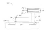
- FIG. 5shows a non-limiting example of the disclosed 1T-1C FeRAM memory cell, similar in construction to a DRAM memory cell, wherein one capacitor and one access transistor form a memory cell. While the dielectric material of DRAM cell capacitor is a linear dielectric material, the dielectric material of FeRAM cell capacitor includes a ferroelectric dielectric material.
- the 1T-1C FeRAM memory cell 500includes a source 504 and a drain 506 formed within a substrate 502 , a conventional transistor acting as an access transistor and comprising a linear dielectric material 545 and a gate electrode 560 , and a capacitor 510 coupled to the drain 506 via an interconnection structure 570 (e.g., a contact plug).
- the capacitor 510comprises a bottom electrode 590 , a top electrode 595 , and a FE crystalline material 540 between the bottom and top electrodes 590 , 595 .
- the FE crystalline material 540may be formed over the bottom electrode 590 using the methods as described earlier for the FE crystalline material 140 of FIG. 1 .
- the crystallization of FE crystalline material 540 into the desired ferroelectric phasemay be performed before forming a top electrode 595 over the FE crystalline material 540 .
- the crystallization of FE crystalline material 540 into the desired ferroelectric phasemay be performed after or at the same time as forming a top electrode 595 over the FE crystalline material 540 .
- the bottom and top electrodes 590 , 595may be any conventional electrode materials.
- the bottom and top electrodes 590 , 595may be formed of the same or different materials.
- the bottom electrode 590may be formed as a continuous material, such as at a thickness ranging from about 20 ⁇ to about 200 ⁇ , from about 50 ⁇ to about 130 ⁇ , or from about 40 ⁇ to about 70 ⁇ . In some embodiments, the bottom electrode 590 has a thickness of about 60 ⁇ .
- FIGS. 1-5show 1T-FeRAM (FeFET) and 1T-1C FeRAM memory cells, it is understood that the present disclosure may be applied to any suitable types of FE memory cells (e.g., 2T-2C FeRAM memory cells). Furthermore, additional acts to form a complete FeRAM device may be performed by conventional fabrication techniques.
- FeFET1T-FeRAM
- 1T-1C FeRAM memory cellsany suitable types of FE memory cells (e.g., 2T-2C FeRAM memory cells).
- additional acts to form a complete FeRAM devicemay be performed by conventional fabrication techniques.
- the disclosed FE crystalline materialsmay exhibit significantly higher remnant polarization (Pr) than perovskite materials that are conventionally used as the FE materials for FE memory devices.
- the disclosed FE crystalline materialsmay be suitable for various FE memory device applications.
- the disclosed FE crystalline materialsmay be used for FERAM devices, or FeFET devices for NAND and NOR applications.
- the disclosed FE crystalline materialsmay satisfy the properties required for use in the FE memory devices, such as high polarization, fast switching speeds, low coercive field, high retention, low fatigue, and low imprint, because of their intrinsic microscopic structure.
- these FE crystalline materialsmay fulfill the extrinsic fabrication requirements, such as low processing temperature, good CMOS compatibility, ease of availability, lower cost, better scalability, etc.
- the semiconductor devicesmay comprise a plurality of FeRAM memory cells arranged in the of a ferroelectric memory cell array.
- additional semiconductor structuresmay be formed in the substrate.
- these additional semiconductor structuresmay include, but not limited to, word line drive circuits, bit line drive circuits, source line drive circuits, sense circuits, or control circuits.
- FIG. 6shows a non-limiting example of a portion of a FeRAM memory cell array.
- the FeRAM memory cell array 600includes a plurality of memory cells 601 , a plurality of digit lines 611 (in dashed lines to show they are buried), and a plurality of word lines 612 (in dashed lines to show they are buried).
- the FeRAM memory cells 601are arranged in rows (coupled to a common digit line 611 ) and in columns (coupled to a common word line 612 ). Individual FeRAM memory cells 601 are located at a cross-point of a digit line 611 and a word line 612 .
- the present disclosuredescribes a ferroelectric memory device including a plurality of memory cells.
- Each of the memory cellscomprises at least one electrode and a ferroelectric crystalline material disposed proximate the at least one electrode.
- the ferroelectric crystalline materialis polarizable by an electric field responsive to an electrical charge of the at least one electrode.
- the ferroelectric crystalline materialhas a polar and chiral crystal structure without inversion symmetry through an inversion center.
- the ferroelectric crystalline materialdoes not consist essentially of an oxide of at least one of hafnium (Hf) and zirconium (Zr).
- the FE memory cells of present disclosuremay exhibit improved cell performance, such as improved cycling, improved data retention, lower ferroelectric coercivity (E c ), and lower electrical field saturation.
- the semiconductor structure of present disclosurecomprising the FE crystalline material may find applications in integrated circuit other than memory devices.
Landscapes
- Semiconductor Memories (AREA)
- Chemical & Material Sciences (AREA)
- Engineering & Computer Science (AREA)
- Materials Engineering (AREA)
- Formation Of Insulating Films (AREA)
- Chemical Vapour Deposition (AREA)
Abstract
Description
- Embodiments of the disclosure relate to the field of semiconductor device design and fabrication. More specifically, embodiments of the disclosure relate to methods of forming ferroelectric memory cells including a ferroelectric material and to related semiconductor device structures, such as memory devices.
- Demands on semiconductor memory devices toward larger storage capacity and faster access speed have continued to increase. Semiconductor memory devices may be categorized into volatile memory devices and non-volatile memory devices. Dynamic Random Access Memory (DRAM) is a prominent volatile memory device, allowing for high speed and high capacity data storage. Examples of non-volatile memory devices include ROM (Read-only-Memory), EEPROM (Electrically Erasable Programmable ROM), FeRAM (Ferroelectric RAM), and MRAM (Magnetoresistive RAM).
- With regard to FeRAM devices, a ferroelectric material is used to store information. The FeRAM devices may include a 1T-1C (1 Transistor-1 Capacitor) memo ry cell design, similar in construction to a DRAM memory cell, wherein one capacitor and one access transistor form a memory cell. While the dielectric material of DRAM cell capacitor is a linear dielectric material, the dielectric material of FeRAM cell capacitor includes a ferroelectric dielectric material. The FeRAM devices may include a 1T (1 Transistor) memory cell design, based on a ferroelectric field effect transistor (FeFET). For FeFET memory cell, the gate isolation material includes a ferroelectric dielectric material.
- Ferroelectric (FE) materials are electrically polarizable materials that possess at least two polarization states, which polarization states may be switched by the application of an external electric field. Each polarization state of FE materials remains stable even after the removal of the applied electric field for at least some period of time. Due to this stability of polarization states, FE materials have been used for memory applications. One of the polarization states is considered to be a logic “1” and the other state a logic “0.” FE materials have a non-linear relationship between the applied electric field and the apparent stored charge, resulting in a ferroelectric characteristic in the form of a hysteresis loop. Several types of FE memory devices have been reported, such as FeRAM devices, and FeFET for NAND and NOR devices.
- Perovskite materials, such as lead zirconate titanate (PZT), have commonly been used as FE materials for the FE memory device applications. However, such conventional FE memory devices often fall short in terms of bit density and scalability because perovskite materials exhibit low remnant polarization (Pr). For FeRAM, the thickness of ferroelectric PZT film must be up to 200 nanometers (nm). Thus, the use of conventional FE materials for the sub 20 nm-FE memory devices has been limited. In addition, conventional FE materials, such as PZT, possess limited compatibility with standard semiconductor processing techniques.
- Thin films of silicon doped hafnium oxide (SiHfO2) in orthorhombic phase have been investigated as an FE material for FE memory devices. However, the orthorhombic phase of SiHfO2is not stable, and certain restrictive processing techniques must be utilized in order to stabilize the orthorhombic phase. For example, a titanium nitride (TiN) top electrode may be formed over the thin film of SiHfO2material, prior to inducing the crystallization of SiHfO2material through a high temperature annealing process. By crystallizing SiHfO2material in the presence of an overlying TiN top electrode cap, the orthorhombic phase of SiHfO2material is formed and stabilized by the mechanically confining (i.e., capping) effect of TiN top electrode, which mechanically strains the underlying SiHfO2material. It has been reported that by using such SiHfO2material as the FE material for an FE memory device, the required thickness of the FE material may be reduced to less than 10 nm.
- U.S. Pat. No. 8,304,823, issued Nov. 6, 2012 to Boescke, discloses a method for manufacturing a ferroelectric memory cell. An amorphous oxide layer of Hf, Zr or (Hf, Zr) is formed over a carrier, and then a covering layer is formed on the amorphous oxide layer. Upon heating the amorphous oxide layer up to a temperature above its crystallization temperature in the confinement of covering layer (i.e., mechanical capping), at least part of the amorphous oxide layer alters its crystal state from amorphous to crystalline, resulting in a crystallized oxide layer that is suitable as a FE material for an FE memory cell.
FIG. 1 is a cross-sectional view of a 1T-FeRAM memory cell in accordance with an embodiment of the present disclosure;FIG. 2 is a cross-sectional view of a 1T-FeRAM memory cell in accordance with another embodiment of the present disclosure;FIG. 3 is a cross-sectional view of a 1T-FeRAM memory cell in accordance with yet another embodiment of the present disclosure;FIG. 4A is a cross-sectional view of a 1T-FeRAM memory cell like that ofFIG. 1 in a quiescent state, wherein the voltages of Vd, Vg, Vs, and Vb are set to 0 V;FIG. 4B is a cross-sectional view of a 1T-FeRAM memory cell like that ofFIG. 1 in a “write 0” operational state, wherein the gate voltage Vg is set to above 0 V, and Vd, Vs, Vb are set to 0 V;FIG. 4C is a cross-sectional views of a 1T-FeRAM memory cell like that ofFIG. 1 in a “write 1” operational state, wherein the gate voltage Vg is set to below 0 V, and Vd, Vs, Vb are set to 0 V;FIG. 5 is a cross-sectional view of a 1T-1C FeRAM memory cell in accordance with another embodiment of the present disclosure; andFIG. 6 is a simplified plan view of a portion of a FeRAM memory cell array in accordance with an embodiment of the present disclosure.- Semiconductor structures are disclosed that include a ferroelectric material comprising a polar and chiral crystal structure without inversion symmetry about an inversion center, wherein the ferroelectric (FE) crystalline material does not consist essentially of an oxide of at least one of hafnium (Hf) and zirconium (Zr). The ferroelectric crystalline material may be doped, mechanically strained, or both to prevent formation of inversion symmetry through an inversion center. Also disclosed are methods of forming a semiconductor structure that includes such ferroelectric material, and related semiconductor devices.
- The following description provides specific details, such as material types, material thicknesses, and processing conditions in order to provide a thorough description of embodiments of the disclosure. However, a person of ordinary skill in the art will understand that the embodiments of the disclosure may be practiced without employing these specific details. Indeed, the embodiments of the disclosure may be practiced in conjunction with conventional fabrication techniques employed in the industry. In addition, the description provided herein does not form a complete process flow for forming a semiconductor device structure, and each of the semiconductor device structures described below do not form a complete semiconductor device. Only those process acts and structures necessary to understand the embodiments of the disclosure are described in detail below. Additional acts to form a complete semiconductor device may be performed by conventional fabrication techniques. Also note, any drawings accompanying the present application are for illustrative purposes only, and are thus not drawn to scale. Additionally, elements common between figures may retain the same numerical designation.
- As used herein, the singular forms “a,” “an,” and “the” are intended to include the plural forms as well, unless the context clearly indicates otherwise.
- As used herein, relational terms, such as “top,” “bottom,” “over,” “under,” etc., are used for clarity and convenience in understanding the disclosure and accompanying drawings and do not connote or depend on any specific preference, orientation, or order, except where the context clearly indicates otherwise.
- As used herein, the term “substrate” means and includes a foundation material or construction upon which components, such as those within a semiconductor device structure are formed. The substrate may be a semiconductor substrate, a base semiconductor material on a supporting structure, a metal electrode, or a semiconductor substrate having one or more materials, structures, or regions formed thereon. The substrate may be a conventional silicon substrate or other bulk substrate including a semiconductive material. As used herein, the term “bulk substrate” means and includes not only silicon wafers, but also silicon-on-insulator (“SOI”) substrates, such as silicon-on-sapphire (“SOS”) substrates or silicon-on-glass (“SOG”) substrates, epitaxial layers of silicon on a base semiconductor foundation, or other semiconductor or optoelectronic materials, such as silicon-germanium (Si1-xGex, where x is, for example, a mole fraction between 0.2 and 0.8), germanium (Ge), gallium arsenide (GaAs), gallium nitride (GaN), or indium phosphide (InP), among others. Furthermore, when reference is made to a “substrate” in the following description, previous process stages may have been utilized to form materials, regions, or junctions in or on the base semiconductor structure or foundation.
- The disclosed ferroelectric materials may be suitable for FeRAM devices. As non-limiting examples, the FeRAM devices may include, but not limited to, a 1T-1C (1 Transistor-1 Capacitor) FE memory cell, or a 1T (1 Transistor) FE memory cell based on a ferroelectric field effect transistor (FeFET).
FIGS. 1-4 show non-limiting examples of 1T-FeRAM memory cells, andFIG. 5 shows a non-limiting example of 1T-1C FeRAM memory cell.FIG. 1 shows a non-limiting example of the disclosed 1T-FeRAM (FeFET) memory cell that is structurally similar to metal-oxide-semiconductor field-effect transistor (MOSFET) with the linear dielectric oxide material replaced by the disclosed FE crystalline material. The 1T-FeRAM memory cell 100 includes asubstrate 102, asource 104, adrain 106, a FEcrystalline material 140 over thesubstrate 102, and agate electrode material 160 over the FEcrystalline material 140.- The FE
crystalline material 140 may include a polar and chiral crystal structure without inversion symmetry through an inversion center, wherein the ferroelectric crystalline material does not consist essentially of an oxide of at least one of hafnium (Hf) and zirconium (Zr). - Upon crystallization, the FE
crystalline material 140 may form polycrystalline microstructrues, wherein at least some grains or crystals within the polycrystalline microstructure have ferroelectric properties. Some grains or crystals within the polycrystalline microstructure may not exhibit ferroelectric properties. In general, the polar, chiral, non-centro-symmetric phase or phases exhibit ferroelectric characteristics. - In some embodiments, the FE
crystalline material 140 may comprise a polar, chiral, non-centro-symmetric phase selected from the group consisting of orthorhombic, tetragonal, cubic, monoclinic, triclinic, trigonal, and hexagonal phases. - In some embodiments, the FE
crystalline material 140 may comprise a polar, chiral, non-centro-symmetric phase selected from the group consisting of orthorhombic and tetragonal phases. - In some embodiments, the FE
crystalline material 140 may comprise a non-centro-symmetric orthorhombic structure corresponding to a space group selected from the group consisting of Pca21, Pbc21, Pmc21, Pmn21, and Pna21. - Non-limiting examples of the FE
crystalline materials 140 having a non-centro-symmetric orthorhombic structure corresponding to Pca21space group may include, but not limited to, V2P2O9, K3Mo3ScO12, BaYCo4O8, CaNa2Al4Si4O16, or LaNa3V2O8. - Non-limiting examples of the FE
crystalline materials 140 having a non-centro-symmetric orthorhombic structure corresponding to Pbc21space group may include, but not limited to, V2P2O9, K3Mo3ScO12, BaYCo4O8, CaNa2Al4Si4O16, or LaNa3V2O8. - Non-limiting examples of the FE
crystalline materials 140 having a non-centro-symmetric orthorhombic structure corresponding to Pmc21space group may include, but not limited to, SnGa4Se7, SeO2, TixTayLazO11where x+y+z=3, or In11Mo40O62. In one embodiment, the FEcrystalline material 140 having a non-centro-symmetric orthorhombic structure corresponding to Pmc21space group may be Ti1.92Ta1.08La3O11. - Non-limiting examples of the FE
crystalline materials 140 having a non-centro-symmetric orthorhombic structure corresponding to Pmn21space group may include, but not limited to, TiSO5, V2O5, Sr5Nb5O16, or ZrMo2O8. - Non-limiting examples of the FE
crystalline materials 140 having a non-centro-symmetric orthorhombic structure corresponding to Pna21space group may include, but not limited to, Si2Y2O7, Sr2P2O7, or Ti0.98Zr0.02RbPO5. - In some embodiments, the FE
crystalline material 140 may comprise a non-centro-symmetric tetragonal structure corresponding to a space group selected from the group consisting of P422, P4212, P4122, P41212, P4222, P42212, P4322, and P43212. - In some embodiments, the FE
crystalline material 140 may be at least substantially free of zirconium and hafnium. - In some embodiments, the FE
crystalline material 140 may be doped, mechanically strained, or both to prevent formation of inversion symmetry through an inversion center. - In some embodiments, the FE
crystalline material 140 may further comprise a ternary or quaternary oxide material selected from the group consisting of Ti1.1Zr0.893Hf0.008O4, Ti1.92Ta1.08La3O11, Sr5Nb5O16, ZrMo2O8, Si2Y2O7, and Ti0.98Zr0.02RbPO5. - In some embodiments, the FE
crystalline material 140 may include at least one dopant selected from the group consisting of yttrium (Y), lanthanum (La), gadolinium (Gd), niobium (Nb), tantalum (Ta), vanadium (V), phosphorus (P), potassium (K), scandium (Sc), rubidium (Rb), selenium (Se), tin (Sn), magnesium (Mg), calcium (Ca), barium (Ba), and indium (In). - The dopants included in the FE crystalline/polycrystalline material may be utilized to increase the endurance of FE memory cell, lower the coercive-field/voltage (Ec/Vc), modulate the capacitance/dielectric constant and its frequency response, enhance the redox resistance at the interfaces or in the relative bulk, reduce the oxygen vacancy generation/migration and redistribution, as well as to stabilize the FE phase leading to increased remnant/spontaneous polarization.
- In some embodiments, the FE
crystalline material 140 may comprise a high-k dielectric material doped with at least one metal selected from the group consisting of gadolinium (Gd), lanthanum (La), vanadium (V), phosphorus (P), potassium (K), scandium (Sc), rubidium (Rb), selenium (Se), tin (Sn), magnesium (Mg), calcium (Ca), barium (Ba), and indium (In). The high-k dielectric material comprises hafnium oxide (HfOx), zirconium oxide (ZrOx), titanium oxide (TiOx), hafnium titanium oxide (HfZrOx), hafnium titanium oxide (HfZrOx), or hafnium silicon oxide (HfSiOx). The FEcrystalline material 140 may comprise the at least one metal in an amount between about 0.5% and about 30% by weight. - In one embodiment, the FE
crystalline material 140 may comprise a high-k dielectric material doped with yttrium (Y), wherein high-k dielectric material comprises hafnium oxide (HfOx), zirconium oxide (ZrOx), titanium oxide (TiOx), hafnium titanium oxide (HfZrOx), hafnium titanium oxide (HfTiOx), or hafnium silicon oxide (HfSiOx). The FEcrystalline material 140 may comprise Y in an amount between about 0.5% and about 25% by weight. - In one embodiment, the FE
crystalline material 140 may comprise a high-k dielectric material doped with strontium (Sr), wherein high-k dielectric material comprises hafnium oxide (HfOx), zirconium oxide (ZrOx), titanium oxide (TiOx), hafnium titanium oxide (HfZrOx), hafnium titanium oxide (HfTiOx), or hafnium silicon oxide (HfSiOx). The FEcrystalline material 140 may comprise Sr in an amount between about 0.05% and about 20% by weight. - In one embodiment, the FE
crystalline material 140 may comprise a high-k dielectric material doped with at least one of niobium (Nb) and tantalum (Ta), wherein high-k dielectric material comprises hafnium oxide (HfOx), zirconium oxide (ZrOx), titanium oxide (TiOx), hafnium titanium oxide (HfZrOx), hafnium titanium oxide (HfTiOx), or hafnium silicon oxide (HfSiOx). At least one of Nb and Ta may be present in the FEcrystalline material 140 in an amount between about 0.2% and about 10% by weight. - The FE
crystalline material 140 may be formed over thesubstrate 102 by any conventional techniques. Non-limiting examples of the conventional techniques may include, but not limited to, atomic layer deposition (ALD), metal organic atomic layer deposition (MOALD), chemical vapor deposition (CVD), metal organic chemical vapor deposition (MOCVD), and physical vapor deposition (PVD). - In some particular embodiments, the FE
crystalline material 140 may be formed over thesubstrate 102 by ALD or MOALD process based on the precursors of the FE metal oxide, oxidant, and, optionally, the dopant capable of interrupting the inversion symmetry of FE metal oxide. The ALD or MOALD process may be performed at a temperature between about 150° C. and about 350° C., and a pressure between about 10 mtorr and about 10 torr. - Various known oxidants may be used for the process. By way of non-limiting examples, the oxidant may include, but not limited to, water vapor (H2O), hydrogen peroxide (H2O2), ozone (O3), or oxygen (O2).
- When the FE
crystalline material 140 comprises Zr-based material, the FEcrystalline material 140 may be formed by ALD process based on any known Zr-precursors. Non-limiting examples of Zr-precursors may include, but not limited to, ZrCl4, C8H24N4Zr, or (C5H5)Zr[N(CH3)2]3. - When the FE
crystalline material 140 comprises Hf-based material, the FEcrystalline material 140 may be formed by ALD process based on any known Hf precursors. Non-limiting examples of Hf-precursors may include, but not limited to, HfCl4, C8H24N4Hf, or (C5H5)Hf[N(CH3)2]3. - When the FE
crystalline material 140 comprises Ti-based material, the FEcrystalline material 140 may be formed by ALD process based on any known Ti precursors. Non-limiting examples of Ti-precursors may include, but not limited to, TiCl4, C8H24N4Ti, or (C5H5)Ti[N(CH3)2]3. - When the FE
crystalline material 140 comprises a dopant, the amount of dopant in the FEcrystalline material 140 may be defined by varying the cycle ratio of the precursors. The content of dopant may be monitored and determined by any conventional techniques and, therefore is not described in detail herein. Non-limiting examples of such techniques may include, but not limited to, secondary ions mass spectrometry, X-ray photoelectron spectroscopy (XPS), high resolution transmission spectroscopy (HR-TEM), etc. In some embodiments, the amount of dopant in the FEcrystalline material 140 may be in a range of about 0.05% to about 30% by weight. The amount of dopant may depend on the thickness of FEcrystalline material 140, the process temperature of 140 ortop electrode 160, or the annealing conditions such as post metallization annealing (PMA) conditions. For example, when increasing the thickness of FEcrystalline material 140, the amount of dopant may also have to be increased to achieve a desired crystallization having ferroelectric properties. - In some embodiments, the thickness of FE
crystalline material 140 may be in a range of about 1 nm to about 100 nm. In some embodiments, the thickness of FEcrystalline material 140 may be in a range of about 2 nm to about 20 nm. - The
gate electrode material 160 may be formed over the FEcrystalline material 140 to provide thesemiconductor structure 100. Thegate electrode material 160 may be fainted over the FEcrystalline material 140 by any conventional techniques. Non-limiting examples of such conventional techniques may include, but not limited to, atomic layer deposition (ALD), plasma enhanced atomic layer deposition (PE-ALD), atomic vapor deposition (AVD), ultraviolet assisted atomic layer deposition (UV-ALD), chemical vapor deposition (CVD), plasma enhanced chemical vapor deposition (PECVD), or physical vapor deposition (PVD). - Any conventional gate electrode material may be used for the
gate electrode material 160. Such materials may comprise an elemental metal, an alloy of two or more elemental metals, a conductive metal compound, a conductively-doped semiconductor material, or mixtures thereof. Non-limiting examples may include, but not limited to, TiN, TiCN, TiAlN, TiAlCN, Ti—W, Ru—TiN, or RuCN. - Accordingly, the present disclosure describes a ferroelectric memory device including a plurality of memory cells. Each of the memory cells comprises at least one electrode and a ferroelectric crystalline material disposed proximate the at least one electrode. The ferroelectric crystalline material is polarizable by an electric field generated by the at least one electrode in an electrically charged state. The ferroelectric crystalline material has a polar and chiral crystal structure without inversion symmetry through an inversion center. The ferroelectric crystalline material comprises a material selected from the group consisting of hafnium oxide (HfOx), zirconium oxide (ZrOx), titanium oxide (TiOx), hafnium zirconium oxide (HfZrOx), hafnium titanium oxide (HfTiOx), and hafnium silicon oxide (HfSiOx). The ferroelectric crystalline material further comprises least one dopant selected from the group consisting of yttrium (Y), strontium (Sr), niobium (Nb), tantalum (Ta), lanthanum (La), gadolinium (Gd), vanadium (V), phosphorus (P), potassium (K), scandium (Sc), rubidium (Rb), selenium (Se), tin (Sn), magnesium (Mg), calcium (Ca), barium (Ba), and indium (In).
- Furthermore, the present disclosure describes a method of forming a semiconductor structure. The method comprises forming a ferroelectric crystalline material over a substrate, and forming at least one electrode proximate the ferroelectric crystalline material. The ferroelectric crystalline material has a polar and chiral crystal structure without inversion symmetry through an inversion center. The ferroelectric crystalline material does not consist essentially of an oxide of at least one of hafnium (Hf) and zirconium (Zr).
- In some embodiments, the method may further comprise annealing the ferroelectric crystalline material and altering a crystal structure of the ferroelectric crystalline material.
- The FE
crystalline material 140 may be annealed to initiate the crystallization into the desired ferroelectric phase. The annealing of FEcrystalline material 140 into the desired ferroelectric phase may be performed by post deposition annealing (PDA) or post metallization annealing (PMA) process. - In the PDA process, the FE
crystalline material 140 is annealed into the desired ferroelectric phase prior to the formation of thegate electrode material 160 over the FEcrystalline material 140. - In the PMA process, the FE
crystalline material 140 is annealed into the desired ferroelectric phase after thegate electrode material 160 is formed over the FEcrystalline material 140. In some embodiments, the PMA annealing may be performed by a rapid thermal processing (RTP) annealing technique under ambient nitrogen (N2) or argon (Ar) condition. - Thus, in some embodiments, the method may further comprise mechanically straining the ferroelectric crystalline material to stabilize the polar and chiral crystal structure of the ferroelectric crystalline material.
- Whether the FE
crystalline material 140 is annealed by PDA or PMA process depends on various factors, including, but not limited to, the types of high-k dielectric material, the types and amounts of dopants, or the desired structures of FE crystalline phase. - The PDA or PMA annealing conditions may be defined based on various controlling factors. By non-limiting examples, such controlling factor may include, but not limited to, the composition of FE
crystalline material 140, the thickness of FEcrystalline material 140, and the composition and thickness ofelectrode material 160 overlying the FE crystalline material140 (in case of PMA process). The relatively thinner FE crystalline/polycrystalline material 140 may require a higher annealing temperature and longer annealing times. The annealing requirement is strongly dependent on the choice ofFE material 140, such that, in some embodiments of present disclosure, the post metallization anneal may be eliminated, with only a post deposition anneal sufficing. In addition to the thickness of FE crystalline/polycrystalline material 140 and/orelectrode material 160, the substrate induced stress may play an important role and may significantly influence the annealing conditions - When the FE
crystalline material 140 comprises at least one dopant, the annealing conditions of the FEcrystalline material 140 may also be a function of the amount and type of dopant present in the FEcrystalline material 140. At relatively higher dopant concentrations, the annealing temperature of the FEcrystalline material 140 may be higher than the annealing temperature of the FEcrystalline material 140 having a lower amount of the dopant. - In the embodiments wherein the FE
crystalline material 140 comprises at least one doped metal selected from the group consisting of gadolinium (Gd), lanthanum (La), vanadium (V), phosphorus (P), potassium (K), scandium (Sc), rubidium (Rb), selenium (Se), tin (Sn), magnesium (Mg), calcium (Ca), barium (Ba), and indium (In), the annealing of the FEcrystalline material 140 may be achieved by PMA annealing at a temperature between about 500° C. and about 800° C. for about 20 seconds to about 600 seconds. - When the FE
crystalline material 140 comprises a high-k dielectric material doped with yttrium (Y), the annealing of the FEcrystalline material 140 may be achieved by post deposition annealing (PDA) or post metallization annealing (PMA) at a temperature between about 450° C. and about 800° C. for about 20 seconds to about 600 seconds. - When the FE
crystalline material 140 comprises a high-k dielectric material doped with strontium (Sr), the annealing of the FEcrystalline material 140 may be achieved by PMA annealing at a temperature between about 450° C. and about 800° C. for about 20 seconds to about 600 seconds. - When the FE
crystalline material 140 comprises a high-k dielectric material doped with at least one of niobium (Nb) and tantalum (Ta), the annealing of the FEcrystalline material 140 may be achieved by PMA annealing at a temperature between about 450° C. and about 800° C. for about 20 seconds to about 300 seconds. - Accordingly, the present disclosure describes a method of forming a semiconductor structure. The method comprises forming a ferroelectric crystalline material over a substrate. The ferroelectric crystalline material has a polar and chiral crystal structure without inversion symmetry through an inversion center. The ferroelectric crystalline material is selected from the group consisting of hafnium oxide (HfOx), zirconium oxide (ZrOx), titanium oxide (TiOx), hafnium zirconium oxide (HfZrOx), hafnium titanium oxide (HfTiOx), and hafnium silicon oxide (HfSiOx). The ferroelectric crystalline material is doped with at least one dopant selected from the group consisting of yttrium (Y), strontium (Sr), niobium (Nb), tantalum (Ta), lanthanum (La), gadolinium (Gd), vanadium (V), phosphorus (P), potassium (K), scandium (Sc), rubidium (Rb), selenium (Se), tin (Sn), magnesium (Mg), calcium (Ca), barium (Ba), and indium (In). The method further comprises forming at least one electrode proximate the ferroelectric crystalline material.
- In some embodiments, the FE
crystalline material 140 may be annealed and crystallized into a stable ferroelectric crystalline phase, without requiring the capping effect to stabilize such ferroelectric crystalline phase. By way of a non-limiting example, such stable ferroelectric crystalline phase may be orthorhombic Pbc21phase. Accordingly, in such embodiments, the crystallization of FEcrystalline material 140 is not necessarily performed in the presence of mechanical confinement (capping) such as those described in U.S. Pat. No. 8,304,823 wherein crystallization of FE crystalline material must be performed in the presence of a covering layer. - Thus, in some embodiments, the method of forming a semiconductor structure comprises crystallizing the FE
crystalline material 140 into a ferroelectric phase without the presence of capping. - The FE
crystalline material 140 may be patterned before crystallizing into the desired ferroelectric phase. Alternatively, the FEcrystalline material 140 may be crystallized into the desired ferroelectric phase prior to or at the same time as patterning the FEcrystalline material 140. The patterning of the FEcrystalline material 140 may be adapted to the intended use of such FEcrystalline material 140. By way of non-limiting examples, the FEcrystalline material 140 may be patterned to define at least part of a gate stack of a 1 T-FeRAM (FeFET) or to define a capacitor dielectric material of 1T-1C FeRAM. FIG. 2 shows another non-limiting example of the disclosed 1T-FeRAM (FeFET) memory cell. 1T-FeRAM memory cell 200 includes asubstrate 202, asource 204, adrain 206, a FEcrystalline material 240 over thesubstrate 202, an insulatingbuffer material 220 between thesubstrate 202 and the FEcrystalline material 240, and agate electrode material 260 over the FEcrystalline material 240. In some embodiments, the insulatingbuffer material 220 may include a crystallized material that is compatible with thesubstrate 202 and the FEcrystalline material 240. In some embodiments, the insulating buffer material may be silicon oxide, such as SiO2, or silicon oxynitride (SiON). In some embodiments, the thickness of the insulatingbuffer material 220 may be in a range between about 0.3 nm to about 6 nm. In some embodiments, the thickness of the insulatingbuffer material 220 may be in a range between about 0.05 nm to about 3 nm.FIG. 3 shows yet another non-limiting example of the disclosed 1T-FERAM (FeFET) memory cell. 1T-FeRAM memory cell 300 includes asubstrate 302, asource 304, adrain 306, a FEcrystalline material 340 over thesubstrate 302, an insulatingbuffer material 320 between thesubstrate 302 and the FEcrystalline material 340, agate electrode material 360 over the FEcrystalline material 340, and aninterfacial material 350 between the FEcrystalline material 340 and thegate electrode material 360.- Accordingly, the present disclosure describes a ferroelectric memory cell. The ferroelectric memory cell comprises a ferroelectric crystalline material having a polar and chiral crystal structure without inversion symmetry through an inversion center. The ferroelectric crystalline material does not consist essentially of an oxide of at least one of hafnium (Hf) and zirconium (Zr).
FIGS. 4A-4C illustrate cross-sectional views of the 1T-FeRAM memory cell 400 that comprises asubstrate 402, asource 404, adrain 406, a FEcrystalline material 440 over thesubstrate 402, and agate electrode material 460 over the FEcrystalline material 440. Thegate electrode material 460 is coupled to a gate voltage Vg; thesource 404 is coupled to a source voltage Vs; thedrain 406 is coupled to a drain voltage Vd; and a bulk region including source/drain 404/406 embedded therein is coupled to a bulk voltage Vb.FIG. 4A shows the 1T-FeRAM memory cell 400 in a quiescent state, wherein the voltages of Vd, Vg, Vs, and Vb are set to zero (0) volt (V).FIG. 4B shows the 1 T-FeRAM memory cell 400 in a “write 0” operational state. The binary information state “0” is written to the 1 T-FeRAM memory cell 400 by setting the gate voltage Vg to above 0 V, and setting Vd, Vs, Vb to 0 V. Hence, an electric field between the bulk (402,404,406) and thegate electrode 460 turns the FEcrystalline material 440 to a first polarization state440B that is associated with the information state “0.” For example, as shown inFIG. 4B , the FE crystalline material440B polarizes such that its dipole moment has a downward arrow direction. When the applied voltage is removed, the polarization state “0” is preserved.FIG. 4C shows the 1T-FeRAM memory cell 400 in a “write 1” operation state. By setting gate voltage Vg to below 0 V and Vd, Vs, Vb to 0 V, the electric field between the bulk (402,404,406) and thegate electrode 460 is reversed and operational state “write 1” is set. In this operation state, the FEcrystalline material 440 is set into a second polarization state440C that is associated with binary information state “1” and is opposite from the first polarization state400B. For example, as shown inFIG. 4C , the FE crystalline material440C polarizes such that its dipole moment has an upward arrow direction. When the applied voltage is removed, the reversed polarization state “1” remains in the FE crystalline material.- Thus, operational states “0” and “1” may be ascribed to different polarization states (440B,440C) of the FE
crystalline material 440. These different polarization states (440B,440C) result in different threshold voltages of the 1T-FeRAM device. - Under a “read” operational state, the information is read from the 1T-
FeRAM memory cell 400 by sensing the current between thesource 404 and thedrain 406. Read-out from the 1T-FeRAM memory cell 400 may be non-destructive. FIG. 5 shows a non-limiting example of the disclosed 1T-1C FeRAM memory cell, similar in construction to a DRAM memory cell, wherein one capacitor and one access transistor form a memory cell. While the dielectric material of DRAM cell capacitor is a linear dielectric material, the dielectric material of FeRAM cell capacitor includes a ferroelectric dielectric material.- As shown in
FIG. 5 , the 1T-1CFeRAM memory cell 500 includes asource 504 and adrain 506 formed within asubstrate 502, a conventional transistor acting as an access transistor and comprising a lineardielectric material 545 and agate electrode 560, and acapacitor 510 coupled to thedrain 506 via an interconnection structure570 (e.g., a contact plug). Thecapacitor 510 comprises abottom electrode 590, atop electrode 595, and a FEcrystalline material 540 between the bottom andtop electrodes - The FE
crystalline material 540 may be formed over thebottom electrode 590 using the methods as described earlier for the FEcrystalline material 140 ofFIG. 1 . The crystallization of FEcrystalline material 540 into the desired ferroelectric phase may be performed before forming atop electrode 595 over the FEcrystalline material 540. Alternatively, the crystallization of FEcrystalline material 540 into the desired ferroelectric phase may be performed after or at the same time as forming atop electrode 595 over the FEcrystalline material 540. - The bottom and
top electrodes top electrodes bottom electrode 590 may be formed as a continuous material, such as at a thickness ranging from about 20 Å to about 200 Å, from about 50 Å to about 130 Å, or from about 40 Å to about 70 Å. In some embodiments, thebottom electrode 590 has a thickness of about 60 Å. - While
FIGS. 1-5 show 1T-FeRAM (FeFET) and 1T-1C FeRAM memory cells, it is understood that the present disclosure may be applied to any suitable types of FE memory cells (e.g., 2T-2C FeRAM memory cells). Furthermore, additional acts to form a complete FeRAM device may be performed by conventional fabrication techniques. - The disclosed FE crystalline materials may exhibit significantly higher remnant polarization (Pr) than perovskite materials that are conventionally used as the FE materials for FE memory devices. Thus, the disclosed FE crystalline materials may be suitable for various FE memory device applications. By way of non-limiting examples, the disclosed FE crystalline materials may be used for FERAM devices, or FeFET devices for NAND and NOR applications.
- The disclosed FE crystalline materials may satisfy the properties required for use in the FE memory devices, such as high polarization, fast switching speeds, low coercive field, high retention, low fatigue, and low imprint, because of their intrinsic microscopic structure. In addition, these FE crystalline materials may fulfill the extrinsic fabrication requirements, such as low processing temperature, good CMOS compatibility, ease of availability, lower cost, better scalability, etc.
- It is to be understood that the cross-sectional views of
FeRAM memory cells FIGS. 1-5 , merely refer to part of the semiconductor devices. Therefore, the semiconductor devices may comprise a plurality of FeRAM memory cells arranged in the of a ferroelectric memory cell array. Furthermore, additional semiconductor structures may be formed in the substrate. By way of non-limiting examples, these additional semiconductor structures may include, but not limited to, word line drive circuits, bit line drive circuits, source line drive circuits, sense circuits, or control circuits. FIG. 6 shows a non-limiting example of a portion of a FeRAM memory cell array. The FeRAMmemory cell array 600 includes a plurality ofmemory cells 601, a plurality of digit lines611 (in dashed lines to show they are buried), and a plurality of word lines612 (in dashed lines to show they are buried). TheFeRAM memory cells 601 are arranged in rows (coupled to a common digit line611) and in columns (coupled to a common word line612). IndividualFeRAM memory cells 601 are located at a cross-point of adigit line 611 and aword line 612.- Accordingly, the present disclosure describes a ferroelectric memory device including a plurality of memory cells. Each of the memory cells comprises at least one electrode and a ferroelectric crystalline material disposed proximate the at least one electrode. The ferroelectric crystalline material is polarizable by an electric field responsive to an electrical charge of the at least one electrode. The ferroelectric crystalline material has a polar and chiral crystal structure without inversion symmetry through an inversion center. The ferroelectric crystalline material does not consist essentially of an oxide of at least one of hafnium (Hf) and zirconium (Zr).
- During use and operation, the FE memory cells of present disclosure may exhibit improved cell performance, such as improved cycling, improved data retention, lower ferroelectric coercivity (Ec), and lower electrical field saturation.
- The semiconductor structure of present disclosure comprising the FE crystalline material may find applications in integrated circuit other than memory devices.
- While the disclosure is susceptible to various modifications and alternative forms, specific embodiments have been shown by way of example in the drawings and have been described in detail herein. However, the disclosure is not intended to be limited to the particular forms disclosed. Rather, the disclosure is to cover all modifications, equivalents, and alternatives falling within the scope of the disclosure as defined by the following appended claims and their legal equivalents.
Claims (29)
Priority Applications (11)
| Application Number | Priority Date | Filing Date | Title |
|---|---|---|---|
| US14/282,520US10242989B2 (en) | 2014-05-20 | 2014-05-20 | Polar, chiral, and non-centro-symmetric ferroelectric materials, memory cells including such materials, and related devices and methods |
| CN201910480089.9ACN110265400A (en) | 2014-05-20 | 2015-04-23 | Ferroelectric devices and forming method thereof |
| PCT/US2015/027308WO2015179062A1 (en) | 2014-05-20 | 2015-04-23 | Polar, chiral, and non-centro-symmetric ferroelectric materials, memory cells including such materials, and related devices and methods |
| CN201580025895.7ACN106463513B (en) | 2014-05-20 | 2015-04-23 | Ferroelectric memory cells and methods of forming semiconductor structures |
| KR1020197011201AKR102099546B1 (en) | 2014-05-20 | 2015-04-23 | Polar, chiral, and non-centro-symmetric ferroelectric materials, memory cells including such materials, and related devices and methods |
| JP2016568022AJP6464401B2 (en) | 2014-05-20 | 2015-04-23 | Polar, chiral, non-centrosymmetric ferroelectric materials, memory cells containing the materials and related devices and methods. |
| KR1020167035388AKR101973248B1 (en) | 2014-05-20 | 2015-04-23 | Polar, chiral, and non-centro-symmetric ferroelectric materials, memory cells including such materials, and related devices and methods |
| EP15796671.4AEP3146566B1 (en) | 2014-05-20 | 2015-04-23 | Polar, chiral, and non-centro-symmetric ferroelectric materials, memory cells including such materials, and related devices and methods |
| TW104114941ATWI603607B (en) | 2014-05-20 | 2015-05-11 | Polar, palm-to-palm and non-centrosymmetric ferroelectric materials, memory cells including the same, and related devices and methods |
| JP2018231727AJP6783290B2 (en) | 2014-05-20 | 2018-12-11 | Polarized, chiral, non-centrosymmetric ferroelectric materials, memory cells containing those materials and related devices and methods |
| US16/284,946US20190189627A1 (en) | 2014-05-20 | 2019-02-25 | Ferroelectric memory cells including ferroelectric crystalline materials having polar and chiral crystal structures, and related memory devices |
Applications Claiming Priority (1)
| Application Number | Priority Date | Filing Date | Title |
|---|---|---|---|
| US14/282,520US10242989B2 (en) | 2014-05-20 | 2014-05-20 | Polar, chiral, and non-centro-symmetric ferroelectric materials, memory cells including such materials, and related devices and methods |
Related Child Applications (1)
| Application Number | Title | Priority Date | Filing Date |
|---|---|---|---|
| US16/284,946DivisionUS20190189627A1 (en) | 2014-05-20 | 2019-02-25 | Ferroelectric memory cells including ferroelectric crystalline materials having polar and chiral crystal structures, and related memory devices |
Publications (2)
| Publication Number | Publication Date |
|---|---|
| US20150340372A1true US20150340372A1 (en) | 2015-11-26 |
| US10242989B2 US10242989B2 (en) | 2019-03-26 |
Family
ID=54554506
Family Applications (2)
| Application Number | Title | Priority Date | Filing Date |
|---|---|---|---|
| US14/282,520ActiveUS10242989B2 (en) | 2014-05-20 | 2014-05-20 | Polar, chiral, and non-centro-symmetric ferroelectric materials, memory cells including such materials, and related devices and methods |
| US16/284,946AbandonedUS20190189627A1 (en) | 2014-05-20 | 2019-02-25 | Ferroelectric memory cells including ferroelectric crystalline materials having polar and chiral crystal structures, and related memory devices |
Family Applications After (1)
| Application Number | Title | Priority Date | Filing Date |
|---|---|---|---|
| US16/284,946AbandonedUS20190189627A1 (en) | 2014-05-20 | 2019-02-25 | Ferroelectric memory cells including ferroelectric crystalline materials having polar and chiral crystal structures, and related memory devices |
Country Status (7)
| Country | Link |
|---|---|
| US (2) | US10242989B2 (en) |
| EP (1) | EP3146566B1 (en) |
| JP (2) | JP6464401B2 (en) |
| KR (2) | KR101973248B1 (en) |
| CN (2) | CN110265400A (en) |
| TW (1) | TWI603607B (en) |
| WO (1) | WO2015179062A1 (en) |
Cited By (44)
| Publication number | Priority date | Publication date | Assignee | Title |
|---|---|---|---|---|
| US20150380641A1 (en)* | 2013-09-25 | 2015-12-31 | Kabushiki Kaisha Toshiba | Semiconductor device and dielectric film |
| US20170103988A1 (en)* | 2015-10-09 | 2017-04-13 | University Of Florida Research Foundation, Inc. | Doped ferroelectric hafnium oxide film devices |
| CN107230676A (en)* | 2017-05-22 | 2017-10-03 | 复旦大学 | The non-volatile ferroelectric memory and its operating method of high read current |
| RU2649622C1 (en)* | 2016-12-23 | 2018-04-04 | Акционерное общество "Научно-исследовательский институт молекулярной электроники" | Ferroelectric memory cell |
| US20180102374A1 (en)* | 2015-12-03 | 2018-04-12 | Micron Technology, Inc. | Ferroelectric Capacitor, Ferroelectric Field Effect Transistor, And Method Used In Forming An Electronic Component Comprising Conductive Material And Ferroelectric Material |
| DE102016015010A1 (en)* | 2016-12-14 | 2018-06-14 | Namlab Ggmbh | An integrated circuit including a ferroelectric memory cell and a manufacturing method therefor |
| KR20180097378A (en)* | 2017-02-23 | 2018-08-31 | 에스케이하이닉스 주식회사 | Ferroelectric Memory Device and Method of Manufacturing the same |
| US10319426B2 (en) | 2017-05-09 | 2019-06-11 | Micron Technology, Inc. | Semiconductor structures, memory cells and devices comprising ferroelectric materials, systems including same, and related methods |
| US20190189627A1 (en)* | 2014-05-20 | 2019-06-20 | Micron Technology, Inc. | Ferroelectric memory cells including ferroelectric crystalline materials having polar and chiral crystal structures, and related memory devices |
| US10396082B2 (en)* | 2017-07-05 | 2019-08-27 | Micron Technology, Inc. | Memory cells having a controlled-conductivity region |
| US10438645B2 (en) | 2017-10-27 | 2019-10-08 | Ferroelectric Memory Gmbh | Memory cell and methods thereof |
| US10460788B2 (en) | 2017-10-27 | 2019-10-29 | Ferroelectric Memory Gmbh | Memory cell and methods thereof |
| CN110504274A (en)* | 2018-05-18 | 2019-11-26 | 瑞萨电子株式会社 | Semiconductor device and method of manufacturing the same |
| WO2020023837A1 (en)* | 2018-07-26 | 2020-01-30 | Tokyo Electron Limited | Method of forming crystallographically stabilized ferroelectric hafnium zirconium based films for semiconductor devices |
| US10600808B2 (en)* | 2017-09-05 | 2020-03-24 | Namlab Ggmbh | Ferroelectric memory cell for an integrated circuit |
| US10872966B1 (en)* | 2019-07-02 | 2020-12-22 | National Taiwan Normal University | Storage memory device |
| CN112133700A (en)* | 2019-06-24 | 2020-12-25 | 无锡拍字节科技有限公司 | Ferroelectric memory device and method of forming the same |
| JP2021503717A (en)* | 2017-11-16 | 2021-02-12 | インターナショナル・ビジネス・マシーンズ・コーポレーションInternational Business Machines Corporation | Hafnium oxide and zirconium oxide based ferroelectric devices with textured iridium bottom electrodes |
| US10923501B2 (en)* | 2017-02-23 | 2021-02-16 | SK Hynix Inc. | Ferroelectric memory device and method of manufacturing the same |
| US20210083121A1 (en)* | 2019-09-18 | 2021-03-18 | Samsung Electronics Co., Ltd. | Electronic device and method of manufacturing the same |
| US20210091227A1 (en)* | 2019-09-24 | 2021-03-25 | Samsung Electronics Co., Ltd. | Domain switching devices and methods of manufacturing the same |
| EP3688815A4 (en)* | 2017-09-28 | 2021-04-14 | INTEL Corporation | FIELD EFFECT TRANSISTORS WITH FERROELECTRIC OR ANTIFERROELECTRIC GATE DIELECTRIC STRUCTURE |
| US20210151445A1 (en)* | 2018-07-31 | 2021-05-20 | Fraunhofer-Gesellschaft Zur Foerderung Der Angewandten Forschung E.V. | Ferroelectric semiconductor device and method for producing a memory cell |
| JP2021520628A (en)* | 2018-04-02 | 2021-08-19 | ラム リサーチ コーポレーションLam Research Corporation | Cap layer for hafnium oxide-based ferroelectric materials |
| US11145740B2 (en)* | 2019-07-23 | 2021-10-12 | National Tsing Hua University | Ferroelectric field effect transistor device |
| US20210359101A1 (en)* | 2020-05-13 | 2021-11-18 | Samsung Electronics Co., Ltd. | Thin film structure and semiconductor device including the same |
| US20210367080A1 (en)* | 2020-05-19 | 2021-11-25 | Samsung Electronics Co., Ltd. | Oxide semiconductor transistor |
| US11289510B2 (en) | 2019-07-25 | 2022-03-29 | Renesas Electronics Corporation | Semiconductor device including ferroelectric film and method of manufacturing the same |
| JPWO2022064306A1 (en)* | 2020-09-22 | 2022-03-31 | ||
| US11322578B2 (en) | 2019-03-06 | 2022-05-03 | Samsung Electronics Co., Ltd. | Semiconductor device |
| DE102021102579A1 (en) | 2020-10-30 | 2022-05-05 | Taiwan Semiconductor Manufacturing Co., Ltd. | MEMORY ARRANGEMENT AND METHOD OF MAKING THIS ARRANGEMENT |
| US20220149206A1 (en)* | 2020-11-12 | 2022-05-12 | Renesas Electronics Corporation | Semiconductor device and method of manufacturing the same |
| US20220271046A1 (en)* | 2021-02-25 | 2022-08-25 | Taiwan Semiconductor Manufacturing Co., Ltd. | Stacked ferroelectric structure |
| US20220285373A1 (en)* | 2021-03-04 | 2022-09-08 | Taiwan Semiconductor Manufacturing Company, Ltd. | Integrated circuit structure and method of forming the same |
| US20220285497A1 (en)* | 2019-12-30 | 2022-09-08 | Unist(Ulsan National Institute Of Science And Technology) | Transistor, ternary inverter comprising same, and transistor manufacturing method |
| US20220336477A1 (en)* | 2021-04-16 | 2022-10-20 | Taiwan Semiconductor Manufacturing Company, Ltd. | Semiconductor devices and method for manufacturing the same |
| US20220376115A1 (en)* | 2020-06-15 | 2022-11-24 | Taiwan Semiconductor Manufacturing Company, Ltd. | Semiconductor device and method of fabricating the same |
| US20230180482A1 (en)* | 2021-12-07 | 2023-06-08 | Intel Corporation | Three-dimensional nanoribbon-based hysteretic memory |
| DE102021214885A1 (en) | 2021-12-22 | 2023-06-22 | Fraunhofer-Gesellschaft zur Förderung der angewandten Forschung eingetragener Verein | Electronic component with at least one layer made of a ferroelectric or antiferroelectric material |
| US20230284454A1 (en)* | 2020-10-16 | 2023-09-07 | Ferroelectric Memory Gmbh | Memory cell and methods thereof |
| US11950430B2 (en) | 2020-10-30 | 2024-04-02 | Ferroelectric Memory Gmbh | Memory cell, capacitive memory structure, and methods thereof |
| US12058849B2 (en) | 2019-11-21 | 2024-08-06 | Intel Corporation | Three-dimensional nanoribbon-based dynamic random-access memory |
| US12075625B2 (en) | 2020-10-30 | 2024-08-27 | Ferroelectric Memory Gmbh | Memory cell, capacitive memory structure, and methods thereof |
| US12382640B2 (en) | 2020-10-30 | 2025-08-05 | Taiwan Semiconductor Manufacturing Company, Ltd. | Memory device and method for fabricating the same |
Families Citing this family (30)
| Publication number | Priority date | Publication date | Assignee | Title |
|---|---|---|---|---|
| CN111900168A (en)* | 2016-01-25 | 2020-11-06 | 中国科学院微电子研究所 | Memory cells, memory devices and electronic equipment |
| US10056393B2 (en)* | 2016-03-01 | 2018-08-21 | Namlab Ggmbh | Application of antiferroelectric like materials in non-volatile memory devices |
| US20190057860A1 (en)* | 2017-08-18 | 2019-02-21 | Lam Research Corporation | Methods for improving performance in hafnium oxide-based ferroelectric material using plasma and/or thermal treatment |
| US10741678B2 (en)* | 2017-10-30 | 2020-08-11 | Taiwan Semiconductor Manufacturing Co., Ltd. | Semiconductor device and manufacturing method thereof |
| CN109817253B (en)* | 2017-11-21 | 2020-11-03 | 上海磁宇信息科技有限公司 | MRAM chip for controlling body potential |
| CN110245749B (en)* | 2018-03-08 | 2024-06-14 | 三星电子株式会社 | Computing unit, neural network and method for performing exclusive nor operation |
| KR102578816B1 (en)* | 2018-03-16 | 2023-09-15 | 에스케이하이닉스 주식회사 | Ferroelectric Memory Device |
| KR102778194B1 (en)* | 2018-08-20 | 2025-03-11 | 삼성전자주식회사 | Logic switching device and method of manufacturing the same |
| CN109920848A (en)* | 2019-03-18 | 2019-06-21 | 西安电子科技大学 | ZrO2-based antiferroelectric memory without interfacial layer |
| CN109979811B (en)* | 2019-03-20 | 2021-09-24 | 电子科技大学 | A kind of preparation method of tantalum-doped hafnium dioxide ferroelectric material |
| CN109935590A (en)* | 2019-03-29 | 2019-06-25 | 湘潭大学 | A 1T1C flexible ferroelectric memory and its preparation method |
| KR20210149162A (en) | 2019-04-08 | 2021-12-08 | 케플러 컴퓨팅 인크. | Doped polar layer and semiconductor device comprising same |
| TWI691078B (en)* | 2019-04-25 | 2020-04-11 | 國立中興大學 | Semiconductor device |
| CN110459611B (en)* | 2019-08-19 | 2022-05-24 | 湘潭大学 | Ferroelectric field effect transistor and preparation method thereof |
| JP7480951B2 (en)* | 2019-10-09 | 2024-05-10 | 国立大学法人京都工芸繊維大学 | Ferroelectric thin film manufacturing method and ferroelectric thin film manufacturing apparatus |
| KR102305342B1 (en)* | 2019-11-14 | 2021-09-24 | 울산과학기술원 | Nonvolatile ternary memory using two-dimensional ferroelectric material and device for manufacturing method thereof |
| CN112928116B (en)* | 2019-12-06 | 2024-03-22 | 财团法人工业技术研究院 | Ferroelectric memory |
| KR20210085460A (en) | 2019-12-30 | 2021-07-08 | 삼성전자주식회사 | Ferroelectric capacitor, transistor, and memory device and fabrication method for the ferroelectric capacitor |
| DE102020119609A1 (en)* | 2020-01-31 | 2021-08-05 | Taiwan Semiconductor Manufacturing Co., Ltd. | NEW GATE STRUCTURES FOR SETTING THE LIMIT VOLTAGE |
| CN111554745B (en)* | 2020-04-23 | 2022-03-08 | 西安电子科技大学 | Ferroelectric capacitor, ferroelectric field effect transistor and preparation method |
| CN111880018B (en)* | 2020-06-29 | 2022-02-11 | 西安交通大学 | Device and method for measuring coercive field strength of ferroelectric crystal |
| JP2022051465A (en)* | 2020-09-18 | 2022-03-31 | キオクシア株式会社 | Semiconductor storage device |
| US12382670B2 (en)* | 2020-11-04 | 2025-08-05 | Samsung Electronics Co., Ltd. | Thin film structure and semiconductor device comprising the same |
| CN112490248B (en)* | 2020-12-03 | 2022-10-21 | 中国科学院微电子研究所 | Ferroelectric floating gate memory cell string and preparation method thereof |
| US12137572B2 (en)* | 2021-02-26 | 2024-11-05 | Taiwan Semiconductor Manufacturing Company, Ltd. | Ferroelectric memory device and method of manufacturing the same |
| JP2022147355A (en) | 2021-03-23 | 2022-10-06 | キオクシア株式会社 | semiconductor storage device |
| CN113808685B (en)* | 2021-08-27 | 2024-01-16 | 西北工业大学深圳研究院 | Analysis method and system for non-centrosymmetric superconducting topological electronic material |
| KR102571133B1 (en)* | 2022-04-26 | 2023-08-25 | 강원대학교산학협력단 | Manufacturing method of ferroelectric device and ferroelectric device |
| WO2024194728A1 (en)* | 2023-03-17 | 2024-09-26 | 株式会社半導体エネルギー研究所 | Semiconductor device |
| KR102845122B1 (en) | 2024-04-18 | 2025-08-13 | 경희대학교 산학협력단 | Multilayer thin film structure |
Citations (6)
| Publication number | Priority date | Publication date | Assignee | Title |
|---|---|---|---|---|
| US4179404A (en)* | 1976-12-15 | 1979-12-18 | Denka Chemical Corporation | Catalyst preparative method |
| US20020015556A1 (en)* | 2000-06-19 | 2002-02-07 | Steinberg Dan A. | Method of fabricating an optical fiber array using photosensitive material |
| US20020115562A1 (en)* | 1999-12-22 | 2002-08-22 | Haldor Topsoe A/S | Process for the synthesis of VPO catalysts |
| US6504214B1 (en)* | 2002-01-11 | 2003-01-07 | Advanced Micro Devices, Inc. | MOSFET device having high-K dielectric layer |
| US20110292574A1 (en)* | 2010-06-01 | 2011-12-01 | Nxp B.V. | High density capacitor |
| US20150179657A1 (en)* | 2013-12-24 | 2015-06-25 | Kabushiki Kaisha Toshiba | Semiconductor storage device |
Family Cites Families (36)
| Publication number | Priority date | Publication date | Assignee | Title |
|---|---|---|---|---|
| ATE223108T1 (en)* | 1995-04-24 | 2002-09-15 | Infineon Technologies Ag | SEMICONDUCTOR STORAGE DEVICE USING A FERROELECTRIC DIELECTRIC AND METHOD FOR PRODUCING |
| US6498362B1 (en)* | 1999-08-26 | 2002-12-24 | Micron Technology, Inc. | Weak ferroelectric transistor |
| JP3939250B2 (en) | 2001-05-10 | 2007-07-04 | シメトリックス・コーポレーション | Ferroelectric composite material, manufacturing method thereof, and memory using the same |
| NO20015735D0 (en)* | 2001-11-23 | 2001-11-23 | Thin Film Electronics Asa | underlayer |
| KR100899497B1 (en) | 2002-09-12 | 2009-05-26 | 교또 다이가꾸 | Thin film and method for manufacturing same |
| JP3873935B2 (en) | 2003-06-18 | 2007-01-31 | セイコーエプソン株式会社 | Ferroelectric memory device |
| JP4257413B2 (en)* | 2003-09-12 | 2009-04-22 | 独立行政法人産業技術総合研究所 | Ferroelectric material |
| JP4713071B2 (en) | 2003-09-12 | 2011-06-29 | トヨタ自動車株式会社 | Fuel cell and manufacturing method thereof |
| US20090039341A1 (en) | 2003-12-22 | 2009-02-12 | Marsman Albert W | Method for the Manufacturing of a Non-Volatile Ferroelectric Memory Device and Memory Device Thus Obtained |
| WO2005064705A1 (en)* | 2003-12-22 | 2005-07-14 | Koninklijke Philips Electronics N.V. | Increasing the wettability of polymer solutions to be deposited on hydrophobic ferroelecric polymerb layers |
| US7172947B2 (en)* | 2004-08-31 | 2007-02-06 | Micron Technology, Inc | High dielectric constant transition metal oxide materials |
| JPWO2006028005A1 (en) | 2004-09-08 | 2008-05-08 | 国立大学法人京都大学 | Ferromagnetic ferroelectric and manufacturing method thereof |
| JP4375560B2 (en) | 2004-12-07 | 2009-12-02 | セイコーエプソン株式会社 | Method for manufacturing transistor-type ferroelectric memory |
| US7253469B2 (en)* | 2005-04-26 | 2007-08-07 | Micron Technology, Inc. | Flash memory device having a graded composition, high dielectric constant gate insulator |
| KR100729231B1 (en)* | 2005-08-03 | 2007-06-15 | 삼성전자주식회사 | Ferroelectric structure, method of forming ferroelectric structure, semiconductor device having ferroelectric structure and manufacturing method thereof |
| CN101384525B (en)* | 2006-02-15 | 2012-09-05 | 巴斯夫欧洲公司 | Dehydrogenation process |
| JP2007243003A (en)* | 2006-03-10 | 2007-09-20 | Oki Electric Ind Co Ltd | Manufacturing method of semiconductor device |
| JP4797717B2 (en) | 2006-03-14 | 2011-10-19 | セイコーエプソン株式会社 | Ferroelectric memory device and method for manufacturing ferroelectric memory device |
| JP4600322B2 (en) | 2006-03-14 | 2010-12-15 | セイコーエプソン株式会社 | Method for manufacturing ferroelectric memory device |
| JP4320679B2 (en) | 2007-02-19 | 2009-08-26 | セイコーエプソン株式会社 | Method for manufacturing ferroelectric memory device |
| US20100135937A1 (en) | 2007-03-26 | 2010-06-03 | The Trustees Of Columbia University In The City Of New York | Metal oxide nanocrystals: preparation and uses |
| JP5253895B2 (en)* | 2007-06-08 | 2013-07-31 | 富士フイルム株式会社 | Ferroelectric film, piezoelectric element, and liquid ejection device |
| US7709359B2 (en) | 2007-09-05 | 2010-05-04 | Qimonda Ag | Integrated circuit with dielectric layer |
| JP2009076571A (en) | 2007-09-19 | 2009-04-09 | Seiko Epson Corp | Ferroelectric capacitor, method of manufacturing the same, and ferroelectric memory device |
| JP2009096772A (en) | 2007-10-18 | 2009-05-07 | Hiroshima Univ | ORGANIC METAL COMPLEX, PROCESS FOR PRODUCING THE SAME, COMPOSITION OF THE ORGANIC METAL COMPLEX SOLUTION, LIQUID CRYSTAL MATERIAL, LIQUID CRYSTAL DEVICE, AND NON-DESTRUCTIVE READABLE MEMORY DEVICE |
| US8304823B2 (en) | 2008-04-21 | 2012-11-06 | Namlab Ggmbh | Integrated circuit including a ferroelectric memory cell and method of manufacturing the same |
| CN101894844B (en) | 2010-06-04 | 2012-05-09 | 清华大学 | Ferroelectric dynamic random access memory based on metal oxide vapor deposition and its preparation method |
| US9373677B2 (en) | 2010-07-07 | 2016-06-21 | Entegris, Inc. | Doping of ZrO2 for DRAM applications |
| KR20120006218A (en)* | 2010-07-12 | 2012-01-18 | 한국전자통신연구원 | Double Gate Nonvolatile Memory Transistor |
| JP2014075159A (en) | 2011-01-27 | 2014-04-24 | Panasonic Corp | Nonvolatile storage and drive method of nonvolatile storage |
| JP5981206B2 (en) | 2012-04-20 | 2016-08-31 | 株式会社東芝 | Semiconductor device manufacturing method and semiconductor manufacturing apparatus |
| JP2014053568A (en) | 2012-09-10 | 2014-03-20 | Toshiba Corp | Ferroelectric memory and method of manufacturing the same |
| JP6121819B2 (en)* | 2013-07-04 | 2017-04-26 | 株式会社東芝 | Semiconductor device and dielectric film |
| JP6067524B2 (en)* | 2013-09-25 | 2017-01-25 | 株式会社東芝 | Semiconductor device and dielectric film |
| JP2015062551A (en) | 2013-09-25 | 2015-04-09 | キヤノン株式会社 | Subject information acquisition device and control method therefor |
| US10242989B2 (en)* | 2014-05-20 | 2019-03-26 | Micron Technology, Inc. | Polar, chiral, and non-centro-symmetric ferroelectric materials, memory cells including such materials, and related devices and methods |
- 2014
- 2014-05-20USUS14/282,520patent/US10242989B2/enactiveActive
- 2015
- 2015-04-23KRKR1020167035388Apatent/KR101973248B1/enactiveActive
- 2015-04-23KRKR1020197011201Apatent/KR102099546B1/enactiveActive
- 2015-04-23WOPCT/US2015/027308patent/WO2015179062A1/enactiveApplication Filing
- 2015-04-23CNCN201910480089.9Apatent/CN110265400A/enactivePending
- 2015-04-23CNCN201580025895.7Apatent/CN106463513B/enactiveActive
- 2015-04-23EPEP15796671.4Apatent/EP3146566B1/enactiveActive
- 2015-04-23JPJP2016568022Apatent/JP6464401B2/enactiveActive
- 2015-05-11TWTW104114941Apatent/TWI603607B/enactive
- 2018
- 2018-12-11JPJP2018231727Apatent/JP6783290B2/enactiveActive
- 2019
- 2019-02-25USUS16/284,946patent/US20190189627A1/ennot_activeAbandoned
Patent Citations (6)
| Publication number | Priority date | Publication date | Assignee | Title |
|---|---|---|---|---|
| US4179404A (en)* | 1976-12-15 | 1979-12-18 | Denka Chemical Corporation | Catalyst preparative method |
| US20020115562A1 (en)* | 1999-12-22 | 2002-08-22 | Haldor Topsoe A/S | Process for the synthesis of VPO catalysts |
| US20020015556A1 (en)* | 2000-06-19 | 2002-02-07 | Steinberg Dan A. | Method of fabricating an optical fiber array using photosensitive material |
| US6504214B1 (en)* | 2002-01-11 | 2003-01-07 | Advanced Micro Devices, Inc. | MOSFET device having high-K dielectric layer |
| US20110292574A1 (en)* | 2010-06-01 | 2011-12-01 | Nxp B.V. | High density capacitor |
| US20150179657A1 (en)* | 2013-12-24 | 2015-06-25 | Kabushiki Kaisha Toshiba | Semiconductor storage device |
Non-Patent Citations (1)
| Title |
|---|
| Hafnium Oxide Based CMOS Compatible Ferroelectric Materials, by Schroeder et al., ECS Journal of Solid State Scienceand Technology, 2 (4) (2013), N69-N72.* |
Cited By (90)
| Publication number | Priority date | Publication date | Assignee | Title |
|---|---|---|---|---|
| US9691973B2 (en)* | 2013-09-25 | 2017-06-27 | Kabushiki Kaisha Toshiba | Semiconductor device and dielectric film including a fluorite-type crystal |
| US20150380641A1 (en)* | 2013-09-25 | 2015-12-31 | Kabushiki Kaisha Toshiba | Semiconductor device and dielectric film |
| US20190189627A1 (en)* | 2014-05-20 | 2019-06-20 | Micron Technology, Inc. | Ferroelectric memory cells including ferroelectric crystalline materials having polar and chiral crystal structures, and related memory devices |
| US10153155B2 (en)* | 2015-10-09 | 2018-12-11 | University Of Florida Research Foundation, Incorporated | Doped ferroelectric hafnium oxide film devices |
| US20170103988A1 (en)* | 2015-10-09 | 2017-04-13 | University Of Florida Research Foundation, Inc. | Doped ferroelectric hafnium oxide film devices |
| US11552086B2 (en) | 2015-12-03 | 2023-01-10 | Micron Technology, Inc. | Ferroelectric capacitor, ferroelectric field effect transistor, and method used in forming an electronic component comprising conductive material and ferroelectric material |
| US10748914B2 (en)* | 2015-12-03 | 2020-08-18 | Micron Technology, Inc. | Ferroelectric capacitor, ferroelectric field effect transistor, and method used in forming an electronic component comprising conductive material and ferroelectric material |
| US20180102374A1 (en)* | 2015-12-03 | 2018-04-12 | Micron Technology, Inc. | Ferroelectric Capacitor, Ferroelectric Field Effect Transistor, And Method Used In Forming An Electronic Component Comprising Conductive Material And Ferroelectric Material |
| US11856790B2 (en) | 2015-12-03 | 2023-12-26 | Micron Technology, Inc. | Ferroelectric capacitors |
| DE102016015010A1 (en)* | 2016-12-14 | 2018-06-14 | Namlab Ggmbh | An integrated circuit including a ferroelectric memory cell and a manufacturing method therefor |
| US10872905B2 (en) | 2016-12-14 | 2020-12-22 | Namlab Ggmbh | Integrated circuit including a ferroelectric memory cell and manufacturing method thereof |
| RU2649622C1 (en)* | 2016-12-23 | 2018-04-04 | Акционерное общество "Научно-исследовательский институт молекулярной электроники" | Ferroelectric memory cell |
| KR102720238B1 (en) | 2017-02-23 | 2024-10-21 | 에스케이하이닉스 주식회사 | Ferroelectric Memory Device and Method of Manufacturing the same |
| US10923501B2 (en)* | 2017-02-23 | 2021-02-16 | SK Hynix Inc. | Ferroelectric memory device and method of manufacturing the same |
| KR20180097378A (en)* | 2017-02-23 | 2018-08-31 | 에스케이하이닉스 주식회사 | Ferroelectric Memory Device and Method of Manufacturing the same |
| US11398263B2 (en) | 2017-05-09 | 2022-07-26 | Micron Technology, Inc. | Semiconductor structures, memory cells and devices comprising ferroelectric materials, systems including same, and related methods |
| US12080329B2 (en) | 2017-05-09 | 2024-09-03 | Micron Technology, Inc. | Ferroelectric devices and ferroelectric memory cells |
| US10319426B2 (en) | 2017-05-09 | 2019-06-11 | Micron Technology, Inc. | Semiconductor structures, memory cells and devices comprising ferroelectric materials, systems including same, and related methods |
| US10726899B2 (en) | 2017-05-09 | 2020-07-28 | Micron Technology, Inc. | Semiconductor structures, memory cells and devices comprising ferroelectric materials, systems including same, and related methods |
| CN107230676A (en)* | 2017-05-22 | 2017-10-03 | 复旦大学 | The non-volatile ferroelectric memory and its operating method of high read current |
| US10665593B2 (en) | 2017-07-05 | 2020-05-26 | Micron Technology, Inc. | Memory cells having a controlled conductivity region |
| US10396082B2 (en)* | 2017-07-05 | 2019-08-27 | Micron Technology, Inc. | Memory cells having a controlled-conductivity region |
| US10600808B2 (en)* | 2017-09-05 | 2020-03-24 | Namlab Ggmbh | Ferroelectric memory cell for an integrated circuit |
| EP3688815A4 (en)* | 2017-09-28 | 2021-04-14 | INTEL Corporation | FIELD EFFECT TRANSISTORS WITH FERROELECTRIC OR ANTIFERROELECTRIC GATE DIELECTRIC STRUCTURE |
| US10622051B2 (en) | 2017-10-27 | 2020-04-14 | Ferroelectric Memory Gmbh | Memory cell and methods thereof |
| US10460788B2 (en) | 2017-10-27 | 2019-10-29 | Ferroelectric Memory Gmbh | Memory cell and methods thereof |
| US10438645B2 (en) | 2017-10-27 | 2019-10-08 | Ferroelectric Memory Gmbh | Memory cell and methods thereof |
| JP7177574B2 (en) | 2017-11-16 | 2022-11-24 | インターナショナル・ビジネス・マシーンズ・コーポレーション | Hafnium Oxide and Zirconium Oxide Based Ferroelectric Devices with Textured Iridium Bottom Electrodes |
| JP2021503717A (en)* | 2017-11-16 | 2021-02-12 | インターナショナル・ビジネス・マシーンズ・コーポレーションInternational Business Machines Corporation | Hafnium oxide and zirconium oxide based ferroelectric devices with textured iridium bottom electrodes |
| JP2021520628A (en)* | 2018-04-02 | 2021-08-19 | ラム リサーチ コーポレーションLam Research Corporation | Cap layer for hafnium oxide-based ferroelectric materials |
| JP7354138B2 (en) | 2018-04-02 | 2023-10-02 | ラム リサーチ コーポレーション | Cap layer for hafnium oxide based ferroelectric materials |
| US10998408B2 (en) | 2018-05-18 | 2021-05-04 | Renesas Electronics Corporation | Semiconductor device and method of manufacturing the same |
| US12389656B2 (en) | 2018-05-18 | 2025-08-12 | Renesas Electronics Corporation | Semiconductor device and method of manufacturing the same |
| US11973119B2 (en) | 2018-05-18 | 2024-04-30 | Renesas Electronics Corporation | Semiconductor device and method of manufacturing the same |
| CN110504274A (en)* | 2018-05-18 | 2019-11-26 | 瑞萨电子株式会社 | Semiconductor device and method of manufacturing the same |
| US10790149B2 (en) | 2018-07-26 | 2020-09-29 | Tokyo Electron Limited | Method of forming crystallographically stabilized ferroelectric hafnium zirconium based films for semiconductor devices |
| TWI809158B (en)* | 2018-07-26 | 2023-07-21 | 日商東京威力科創股份有限公司 | Method of forming crystallographically stabilized ferroelectric hafnium zirconium based films for semiconductor devices |
| WO2020023837A1 (en)* | 2018-07-26 | 2020-01-30 | Tokyo Electron Limited | Method of forming crystallographically stabilized ferroelectric hafnium zirconium based films for semiconductor devices |
| US11672127B2 (en)* | 2018-07-31 | 2023-06-06 | Fraunhofer-Gesellschaft Zur Foerderung Der Angewandten Forschung E.V. | Ferroelectric semiconductor device and method for producing a memory cell |
| US20210151445A1 (en)* | 2018-07-31 | 2021-05-20 | Fraunhofer-Gesellschaft Zur Foerderung Der Angewandten Forschung E.V. | Ferroelectric semiconductor device and method for producing a memory cell |
| US12125872B2 (en) | 2019-03-06 | 2024-10-22 | Samsung Electronics Co., Ltd. | Semiconductor device |
| US11728372B2 (en) | 2019-03-06 | 2023-08-15 | Samsung Electronics Co., Ltd. | Semiconductor device |
| US11322578B2 (en) | 2019-03-06 | 2022-05-03 | Samsung Electronics Co., Ltd. | Semiconductor device |
| CN112133700A (en)* | 2019-06-24 | 2020-12-25 | 无锡拍字节科技有限公司 | Ferroelectric memory device and method of forming the same |
| EP3966864A4 (en)* | 2019-06-24 | 2022-06-22 | Wuxi Petabyte Technologies Co., Ltd. | Ferroelectric memory devices and methods for forming the same |
| US10872966B1 (en)* | 2019-07-02 | 2020-12-22 | National Taiwan Normal University | Storage memory device |
| US11145740B2 (en)* | 2019-07-23 | 2021-10-12 | National Tsing Hua University | Ferroelectric field effect transistor device |
| US11289510B2 (en) | 2019-07-25 | 2022-03-29 | Renesas Electronics Corporation | Semiconductor device including ferroelectric film and method of manufacturing the same |
| US20210083121A1 (en)* | 2019-09-18 | 2021-03-18 | Samsung Electronics Co., Ltd. | Electronic device and method of manufacturing the same |
| US11824118B2 (en)* | 2019-09-18 | 2023-11-21 | Samsung Electronics Co., Ltd. | Electronic device and method of manufacturing the same |
| US12230711B2 (en)* | 2019-09-18 | 2025-02-18 | Samsung Electronics Co., Ltd. | Electronic device and method of manufacturing the same |
| US11522082B2 (en)* | 2019-09-18 | 2022-12-06 | Samsung Electronics Co., Ltd. | Electronic device and method of manufacturing the same |
| US20240038891A1 (en)* | 2019-09-18 | 2024-02-01 | Samsung Electronics Co., Ltd. | Electronic device and method of manufacturing the same |
| US12224346B2 (en) | 2019-09-24 | 2025-02-11 | Samsung Electronics Co., Ltd. | Domain switching devices and methods of manufacturing the same |
| US11527646B2 (en)* | 2019-09-24 | 2022-12-13 | Samsung Electronics Co., Ltd. | Domain switching devices and methods of manufacturing the same |
| US11824119B2 (en) | 2019-09-24 | 2023-11-21 | Samsung Electronics Co., Ltd. | Domain switching devices and methods of manufacturing the same |
| US20210091227A1 (en)* | 2019-09-24 | 2021-03-25 | Samsung Electronics Co., Ltd. | Domain switching devices and methods of manufacturing the same |
| US12058849B2 (en) | 2019-11-21 | 2024-08-06 | Intel Corporation | Three-dimensional nanoribbon-based dynamic random-access memory |
| US20220285497A1 (en)* | 2019-12-30 | 2022-09-08 | Unist(Ulsan National Institute Of Science And Technology) | Transistor, ternary inverter comprising same, and transistor manufacturing method |
| US12154950B2 (en)* | 2019-12-30 | 2024-11-26 | Unist (Ulsan National Institute Of Science And Technology) | Transistor, ternary inverter comprising same, and transistor manufacturing method |
| US12107140B2 (en) | 2020-05-13 | 2024-10-01 | Samsung Electronics Co., Ltd. | Thin film structure and semiconductor device including the same |
| US20210359101A1 (en)* | 2020-05-13 | 2021-11-18 | Samsung Electronics Co., Ltd. | Thin film structure and semiconductor device including the same |
| US11804536B2 (en)* | 2020-05-13 | 2023-10-31 | Samsung Electronics Co., Ltd. | Thin film structure and semiconductor device including the same |
| US11824117B2 (en)* | 2020-05-19 | 2023-11-21 | Samsung Electronics Co., Ltd. | Oxide semiconductor transistor |
| US20210367080A1 (en)* | 2020-05-19 | 2021-11-25 | Samsung Electronics Co., Ltd. | Oxide semiconductor transistor |
| US20220376115A1 (en)* | 2020-06-15 | 2022-11-24 | Taiwan Semiconductor Manufacturing Company, Ltd. | Semiconductor device and method of fabricating the same |
| US12363957B2 (en)* | 2020-06-15 | 2025-07-15 | Taiwan Semiconductor Manufacturing Company, Ltd. | Semiconductor device and method of fabricating the same |
| US11901451B2 (en)* | 2020-06-15 | 2024-02-13 | Taiwan Semiconductor Manufacturing Company, Ltd. | Method of fabricating semiconductor device |
| JPWO2022064306A1 (en)* | 2020-09-22 | 2022-03-31 | ||
| US20230284454A1 (en)* | 2020-10-16 | 2023-09-07 | Ferroelectric Memory Gmbh | Memory cell and methods thereof |
| US11706928B2 (en)* | 2020-10-30 | 2023-07-18 | Taiwan Semiconductor Manufacturing Company, Ltd. | Memory device and method for fabricating the same |
| US12382640B2 (en) | 2020-10-30 | 2025-08-05 | Taiwan Semiconductor Manufacturing Company, Ltd. | Memory device and method for fabricating the same |
| DE102021102579A1 (en) | 2020-10-30 | 2022-05-05 | Taiwan Semiconductor Manufacturing Co., Ltd. | MEMORY ARRANGEMENT AND METHOD OF MAKING THIS ARRANGEMENT |
| US11950430B2 (en) | 2020-10-30 | 2024-04-02 | Ferroelectric Memory Gmbh | Memory cell, capacitive memory structure, and methods thereof |
| US12075625B2 (en) | 2020-10-30 | 2024-08-27 | Ferroelectric Memory Gmbh | Memory cell, capacitive memory structure, and methods thereof |
| US20220149206A1 (en)* | 2020-11-12 | 2022-05-12 | Renesas Electronics Corporation | Semiconductor device and method of manufacturing the same |
| US12009425B2 (en)* | 2020-11-12 | 2024-06-11 | Renesas Electronics Corporation | Semiconductor device and method of manufacturing the same |
| US12232329B2 (en)* | 2021-02-25 | 2025-02-18 | Taiwan Semiconductor Manufacturing Company, Ltd. | Stacked ferroelectric structure |
| US11508755B2 (en)* | 2021-02-25 | 2022-11-22 | Taiwan Semiconductor Manufacturing Company, Ltd. | Stacked ferroelectric structure |
| US20220271046A1 (en)* | 2021-02-25 | 2022-08-25 | Taiwan Semiconductor Manufacturing Co., Ltd. | Stacked ferroelectric structure |
| US20230371272A1 (en)* | 2021-02-25 | 2023-11-16 | Taiwan Semiconductor Manufacturing Company, Ltd. | Stacked ferroelectric structure |
| US12207474B2 (en) | 2021-02-25 | 2025-01-21 | Taiwan Semiconductor Manufacturing Company, Ltd. | Stacked ferroelectric structure |
| US11557609B2 (en)* | 2021-03-04 | 2023-01-17 | Taiwan Semiconductor Manufacturing Company, Ltd. | Integrated circuit structure and method of forming the same |
| US20220285373A1 (en)* | 2021-03-04 | 2022-09-08 | Taiwan Semiconductor Manufacturing Company, Ltd. | Integrated circuit structure and method of forming the same |
| US20220336477A1 (en)* | 2021-04-16 | 2022-10-20 | Taiwan Semiconductor Manufacturing Company, Ltd. | Semiconductor devices and method for manufacturing the same |
| US11574927B2 (en)* | 2021-04-16 | 2023-02-07 | Taiwan Semiconductor Manufacturing Company, Ltd. | Semiconductor devices and method for manufacturing the same |
| US20230180482A1 (en)* | 2021-12-07 | 2023-06-08 | Intel Corporation | Three-dimensional nanoribbon-based hysteretic memory |
| EP4195900A1 (en)* | 2021-12-07 | 2023-06-14 | INTEL Corporation | Three-dimensional nanoribbon-based hysteretic memory |
| DE102021214885A1 (en) | 2021-12-22 | 2023-06-22 | Fraunhofer-Gesellschaft zur Förderung der angewandten Forschung eingetragener Verein | Electronic component with at least one layer made of a ferroelectric or antiferroelectric material |
| DE102021214885B4 (en) | 2021-12-22 | 2023-10-05 | Fraunhofer-Gesellschaft zur Förderung der angewandten Forschung eingetragener Verein | Electronic component with at least one layer made of a ferroelectric or antiferroelectric material |
Also Published As
| Publication number | Publication date |
|---|---|
| JP2019057727A (en) | 2019-04-11 |
| CN110265400A (en) | 2019-09-20 |
| WO2015179062A1 (en) | 2015-11-26 |
| KR102099546B1 (en) | 2020-04-10 |
| TW201546803A (en) | 2015-12-16 |
| EP3146566A4 (en) | 2018-05-30 |
| JP2017518639A (en) | 2017-07-06 |
| JP6783290B2 (en) | 2020-11-11 |
| CN106463513B (en) | 2019-06-28 |
| KR20190043641A (en) | 2019-04-26 |
| TWI603607B (en) | 2017-10-21 |
| KR101973248B1 (en) | 2019-04-26 |
| JP6464401B2 (en) | 2019-02-06 |
| CN106463513A (en) | 2017-02-22 |
| EP3146566B1 (en) | 2022-03-16 |
| US20190189627A1 (en) | 2019-06-20 |
| EP3146566A1 (en) | 2017-03-29 |
| KR20170007811A (en) | 2017-01-20 |
| US10242989B2 (en) | 2019-03-26 |
Similar Documents
| Publication | Publication Date | Title |
|---|---|---|
| US20190189627A1 (en) | Ferroelectric memory cells including ferroelectric crystalline materials having polar and chiral crystal structures, and related memory devices | |
| US10600808B2 (en) | Ferroelectric memory cell for an integrated circuit | |
| US20250098175A1 (en) | Electronic devices including ferroelectric materials, and related memory devices | |
| CN111295735B (en) | Ferroelectric device based on hafnium oxide and zirconium oxide with textured iridium bottom electrode | |
| EP3910687A1 (en) | Thin film structure and semiconductor device including the same | |
| US10043567B2 (en) | Multilevel ferroelectric memory cell for an integrated circuit | |
| US9053802B2 (en) | Ferroelectric memory cell for an integrated circuit | |
| US10319426B2 (en) | Semiconductor structures, memory cells and devices comprising ferroelectric materials, systems including same, and related methods | |
| US9871044B2 (en) | Enhanced charge storage materials, related semiconductor memory cells and semiconductor devices, and related systems and methods | |
| KR102834075B1 (en) | Inserting inhibition layer for inducing antiferroelectricity to ferroelectric structure | |
| TWI859692B (en) | Methods of forming ferroelectric devices and semiconductor device structure | |
| US12408349B2 (en) | Ferroelectric tunnel junctions with conductive electrodes having asymmetric nitrogen or oxygen profiles | |
| CN117580364A (en) | Ferroelectric structure, integrated circuit and forming method thereof |
Legal Events
| Date | Code | Title | Description |
|---|---|---|---|
| AS | Assignment | Owner name:MICRON TECHNOLOGY, INC., IDAHO Free format text:ASSIGNMENT OF ASSIGNORS INTEREST;ASSIGNORS:PANDEY, SUMEET C.;BI, LEI;MEADE, ROY E.;AND OTHERS;SIGNING DATES FROM 20140505 TO 20140513;REEL/FRAME:032962/0397 | |
| AS | Assignment | Owner name:U.S. BANK NATIONAL ASSOCIATION, AS COLLATERAL AGENT, CALIFORNIA Free format text:SECURITY INTEREST;ASSIGNOR:MICRON TECHNOLOGY, INC.;REEL/FRAME:038669/0001 Effective date:20160426 Owner name:U.S. BANK NATIONAL ASSOCIATION, AS COLLATERAL AGEN Free format text:SECURITY INTEREST;ASSIGNOR:MICRON TECHNOLOGY, INC.;REEL/FRAME:038669/0001 Effective date:20160426 | |
| AS | Assignment | Owner name:MORGAN STANLEY SENIOR FUNDING, INC., AS COLLATERAL AGENT, MARYLAND Free format text:PATENT SECURITY AGREEMENT;ASSIGNOR:MICRON TECHNOLOGY, INC.;REEL/FRAME:038954/0001 Effective date:20160426 Owner name:MORGAN STANLEY SENIOR FUNDING, INC., AS COLLATERAL Free format text:PATENT SECURITY AGREEMENT;ASSIGNOR:MICRON TECHNOLOGY, INC.;REEL/FRAME:038954/0001 Effective date:20160426 | |
| AS | Assignment | Owner name:U.S. BANK NATIONAL ASSOCIATION, AS COLLATERAL AGENT, CALIFORNIA Free format text:CORRECTIVE ASSIGNMENT TO CORRECT THE REPLACE ERRONEOUSLY FILED PATENT #7358718 WITH THE CORRECT PATENT #7358178 PREVIOUSLY RECORDED ON REEL 038669 FRAME 0001. ASSIGNOR(S) HEREBY CONFIRMS THE SECURITY INTEREST;ASSIGNOR:MICRON TECHNOLOGY, INC.;REEL/FRAME:043079/0001 Effective date:20160426 Owner name:U.S. BANK NATIONAL ASSOCIATION, AS COLLATERAL AGEN Free format text:CORRECTIVE ASSIGNMENT TO CORRECT THE REPLACE ERRONEOUSLY FILED PATENT #7358718 WITH THE CORRECT PATENT #7358178 PREVIOUSLY RECORDED ON REEL 038669 FRAME 0001. ASSIGNOR(S) HEREBY CONFIRMS THE SECURITY INTEREST;ASSIGNOR:MICRON TECHNOLOGY, INC.;REEL/FRAME:043079/0001 Effective date:20160426 | |
| AS | Assignment | Owner name:JPMORGAN CHASE BANK, N.A., AS COLLATERAL AGENT, ILLINOIS Free format text:SECURITY INTEREST;ASSIGNORS:MICRON TECHNOLOGY, INC.;MICRON SEMICONDUCTOR PRODUCTS, INC.;REEL/FRAME:047540/0001 Effective date:20180703 Owner name:JPMORGAN CHASE BANK, N.A., AS COLLATERAL AGENT, IL Free format text:SECURITY INTEREST;ASSIGNORS:MICRON TECHNOLOGY, INC.;MICRON SEMICONDUCTOR PRODUCTS, INC.;REEL/FRAME:047540/0001 Effective date:20180703 | |
| AS | Assignment | Owner name:MICRON TECHNOLOGY, INC., IDAHO Free format text:RELEASE BY SECURED PARTY;ASSIGNOR:U.S. BANK NATIONAL ASSOCIATION, AS COLLATERAL AGENT;REEL/FRAME:047243/0001 Effective date:20180629 | |
| STCF | Information on status: patent grant | Free format text:PATENTED CASE | |
| CC | Certificate of correction | ||
| AS | Assignment | Owner name:MICRON TECHNOLOGY, INC., IDAHO Free format text:RELEASE BY SECURED PARTY;ASSIGNOR:MORGAN STANLEY SENIOR FUNDING, INC., AS COLLATERAL AGENT;REEL/FRAME:050937/0001 Effective date:20190731 | |
| AS | Assignment | Owner name:MICRON TECHNOLOGY, INC., IDAHO Free format text:RELEASE BY SECURED PARTY;ASSIGNOR:JPMORGAN CHASE BANK, N.A., AS COLLATERAL AGENT;REEL/FRAME:051028/0001 Effective date:20190731 Owner name:MICRON SEMICONDUCTOR PRODUCTS, INC., IDAHO Free format text:RELEASE BY SECURED PARTY;ASSIGNOR:JPMORGAN CHASE BANK, N.A., AS COLLATERAL AGENT;REEL/FRAME:051028/0001 Effective date:20190731 | |
| MAFP | Maintenance fee payment | Free format text:PAYMENT OF MAINTENANCE FEE, 4TH YEAR, LARGE ENTITY (ORIGINAL EVENT CODE: M1551); ENTITY STATUS OF PATENT OWNER: LARGE ENTITY Year of fee payment:4 |