US20150303056A1 - Conformal deposition of silicon carbide films - Google Patents
Conformal deposition of silicon carbide filmsDownload PDFInfo
- Publication number
- US20150303056A1 US20150303056A1US14/616,435US201514616435AUS2015303056A1US 20150303056 A1US20150303056 A1US 20150303056A1US 201514616435 AUS201514616435 AUS 201514616435AUS 2015303056 A1US2015303056 A1US 2015303056A1
- Authority
- US
- United States
- Prior art keywords
- silicon
- bonds
- silicon carbide
- containing precursor
- carbon
- Prior art date
- Legal status (The legal status is an assumption and is not a legal conclusion. Google has not performed a legal analysis and makes no representation as to the accuracy of the status listed.)
- Granted
Links
- HBMJWWWQQXIZIP-UHFFFAOYSA-Nsilicon carbideChemical group[Si+]#[C-]HBMJWWWQQXIZIP-UHFFFAOYSA-N0.000titleclaimsabstractdescription148
- 229910010271silicon carbideInorganic materials0.000titleclaimsabstractdescription143
- 230000008021depositionEffects0.000titleclaimsdescription27
- 239000002243precursorSubstances0.000claimsabstractdescription159
- XUIMIQQOPSSXEZ-UHFFFAOYSA-NSiliconChemical compound[Si]XUIMIQQOPSSXEZ-UHFFFAOYSA-N0.000claimsabstractdescription119
- 229910052710siliconInorganic materials0.000claimsabstractdescription107
- 239000010703siliconSubstances0.000claimsabstractdescription98
- 238000000034methodMethods0.000claimsabstractdescription79
- 150000003254radicalsChemical class0.000claimsabstractdescription54
- 239000001257hydrogenSubstances0.000claimsabstractdescription50
- 229910052739hydrogenInorganic materials0.000claimsabstractdescription50
- 239000010408filmSubstances0.000claimsdescription139
- 239000000758substrateSubstances0.000claimsdescription66
- 238000000151depositionMethods0.000claimsdescription51
- -1cyclic siloxaneChemical class0.000claimsdescription50
- 238000006243chemical reactionMethods0.000claimsdescription48
- IJGRMHOSHXDMSA-UHFFFAOYSA-NAtomic nitrogenChemical compoundN#NIJGRMHOSHXDMSA-UHFFFAOYSA-N0.000claimsdescription43
- 239000007789gasSubstances0.000claimsdescription42
- 239000001301oxygenSubstances0.000claimsdescription30
- 229910052760oxygenInorganic materials0.000claimsdescription30
- QVGXLLKOCUKJST-UHFFFAOYSA-Natomic oxygenChemical compound[O]QVGXLLKOCUKJST-UHFFFAOYSA-N0.000claimsdescription29
- 229910052757nitrogenInorganic materials0.000claimsdescription21
- 125000004435hydrogen atomChemical group[H]*0.000claimsdescription20
- KPUWHANPEXNPJT-UHFFFAOYSA-NdisiloxaneChemical class[SiH3]O[SiH3]KPUWHANPEXNPJT-UHFFFAOYSA-N0.000claimsdescription17
- 125000003545alkoxy groupChemical group0.000claimsdescription12
- 150000001343alkyl silanesChemical group0.000claimsdescription11
- 239000010409thin filmSubstances0.000claimsdescription9
- QGZKDVFQNNGYKY-UHFFFAOYSA-NAmmoniaChemical compoundNQGZKDVFQNNGYKY-UHFFFAOYSA-N0.000claimsdescription8
- 238000000231atomic layer depositionMethods0.000claimsdescription8
- 150000001875compoundsChemical class0.000claimsdescription8
- OBNDGIHQAIXEAO-UHFFFAOYSA-N[O].[Si]Chemical compound[O].[Si]OBNDGIHQAIXEAO-UHFFFAOYSA-N0.000claimsdescription7
- 125000003277amino groupChemical group0.000claimsdescription7
- SNYNNFDVNITLRQ-UHFFFAOYSA-N2,2,4,4,6,6,8-heptamethyl-1,3,5,7,2,4,6,8$l^{3}-tetraoxatetrasilocaneChemical compoundC[Si]1O[Si](C)(C)O[Si](C)(C)O[Si](C)(C)O1SNYNNFDVNITLRQ-UHFFFAOYSA-N0.000claimsdescription6
- WZJUBBHODHNQPW-UHFFFAOYSA-N2,4,6,8-tetramethyl-1,3,5,7,2$l^{3},4$l^{3},6$l^{3},8$l^{3}-tetraoxatetrasilocaneChemical compoundC[Si]1O[Si](C)O[Si](C)O[Si](C)O1WZJUBBHODHNQPW-UHFFFAOYSA-N0.000claimsdescription5
- 150000002431hydrogenChemical class0.000claimsdescription5
- 229910021529ammoniaInorganic materials0.000claimsdescription4
- PZPGRFITIJYNEJ-UHFFFAOYSA-NdisilaneChemical compound[SiH3][SiH3]PZPGRFITIJYNEJ-UHFFFAOYSA-N0.000claimsdescription4
- 150000002831nitrogen free-radicalsChemical class0.000claimsdescription4
- VEDJZFSRVVQBIL-UHFFFAOYSA-NtrisilaneChemical compound[SiH3][SiH2][SiH3]VEDJZFSRVVQBIL-UHFFFAOYSA-N0.000claimsdescription2
- 230000008569processEffects0.000abstractdescription47
- 210000002381plasmaAnatomy0.000description68
- 239000010410layerSubstances0.000description30
- 229910052799carbonInorganic materials0.000description23
- 239000000376reactantSubstances0.000description23
- 238000012545processingMethods0.000description21
- 241000894007speciesSpecies0.000description21
- OKTJSMMVPCPJKN-UHFFFAOYSA-NCarbonChemical compound[C]OKTJSMMVPCPJKN-UHFFFAOYSA-N0.000description19
- UFHFLCQGNIYNRP-UHFFFAOYSA-NHydrogenChemical compound[H][H]UFHFLCQGNIYNRP-UHFFFAOYSA-N0.000description18
- 239000011148porous materialSubstances0.000description18
- 235000012431wafersNutrition0.000description18
- 239000004065semiconductorSubstances0.000description15
- RYGMFSIKBFXOCR-UHFFFAOYSA-NCopperChemical compound[Cu]RYGMFSIKBFXOCR-UHFFFAOYSA-N0.000description14
- 229910052802copperInorganic materials0.000description14
- 239000010949copperSubstances0.000description14
- CURLTUGMZLYLDI-UHFFFAOYSA-NCarbon dioxideChemical compoundO=C=OCURLTUGMZLYLDI-UHFFFAOYSA-N0.000description13
- 239000003989dielectric materialSubstances0.000description13
- 238000004519manufacturing processMethods0.000description13
- 229910052751metalInorganic materials0.000description10
- 239000002184metalSubstances0.000description10
- 238000009792diffusion processMethods0.000description9
- 239000000203mixtureSubstances0.000description9
- 239000000126substanceSubstances0.000description9
- 125000000217alkyl groupChemical group0.000description8
- 230000004888barrier functionEffects0.000description8
- 239000001569carbon dioxideSubstances0.000description8
- 229910002092carbon dioxideInorganic materials0.000description8
- 239000012634fragmentSubstances0.000description8
- 230000005283ground stateEffects0.000description8
- 150000002430hydrocarbonsChemical group0.000description8
- 239000000463materialSubstances0.000description8
- 238000000623plasma-assisted chemical vapour depositionMethods0.000description8
- 125000004122cyclic groupChemical group0.000description7
- 239000001307heliumSubstances0.000description7
- 229910052734heliumInorganic materials0.000description7
- SWQJXJOGLNCZEY-UHFFFAOYSA-Nhelium atomChemical compound[He]SWQJXJOGLNCZEY-UHFFFAOYSA-N0.000description7
- YZCKVEUIGOORGS-IGMARMGPSA-NProtiumChemical compound[1H]YZCKVEUIGOORGS-IGMARMGPSA-N0.000description6
- HMDDXIMCDZRSNE-UHFFFAOYSA-N[C].[Si]Chemical compound[C].[Si]HMDDXIMCDZRSNE-UHFFFAOYSA-N0.000description6
- 125000004429atomChemical group0.000description6
- 239000012159carrier gasSubstances0.000description6
- XUKFPAQLGOOCNJ-UHFFFAOYSA-Ndimethyl(trimethylsilyloxy)siliconChemical compoundC[Si](C)O[Si](C)(C)CXUKFPAQLGOOCNJ-UHFFFAOYSA-N0.000description6
- 150000002500ionsChemical class0.000description6
- 238000001465metallisationMethods0.000description6
- NJPPVKZQTLUDBO-UHFFFAOYSA-NnovaluronChemical compoundC1=C(Cl)C(OC(F)(F)C(OC(F)(F)F)F)=CC=C1NC(=O)NC(=O)C1=C(F)C=CC=C1FNJPPVKZQTLUDBO-UHFFFAOYSA-N0.000description6
- UHUUYVZLXJHWDV-UHFFFAOYSA-Ntrimethyl(methylsilyloxy)silaneChemical compoundC[SiH2]O[Si](C)(C)CUHUUYVZLXJHWDV-UHFFFAOYSA-N0.000description6
- UMVBXBACMIOFDO-UHFFFAOYSA-N[N].[Si]Chemical compound[N].[Si]UMVBXBACMIOFDO-UHFFFAOYSA-N0.000description5
- 238000011084recoveryMethods0.000description5
- 239000000565sealantSubstances0.000description5
- GQPLMRYTRLFLPF-UHFFFAOYSA-NNitrous OxideChemical compound[O-][N+]#NGQPLMRYTRLFLPF-UHFFFAOYSA-N0.000description4
- BLRPTPMANUNPDV-UHFFFAOYSA-NSilaneChemical class[SiH4]BLRPTPMANUNPDV-UHFFFAOYSA-N0.000description4
- 125000004432carbon atomChemical groupC*0.000description4
- 230000015556catabolic processEffects0.000description4
- 238000005229chemical vapour depositionMethods0.000description4
- 238000004132cross linkingMethods0.000description4
- 230000000694effectsEffects0.000description4
- 230000001590oxidative effectEffects0.000description4
- 125000004430oxygen atomChemical groupO*0.000description4
- 238000011112process operationMethods0.000description4
- SBEQWOXEGHQIMW-UHFFFAOYSA-NsiliconChemical compound[Si].[Si]SBEQWOXEGHQIMW-UHFFFAOYSA-N0.000description4
- OKKJLVBELUTLKV-UHFFFAOYSA-NMethanolChemical compoundOCOKKJLVBELUTLKV-UHFFFAOYSA-N0.000description3
- 125000002355alkine groupChemical group0.000description3
- DDJSWKLBKSLAAZ-UHFFFAOYSA-NcyclotetrasiloxaneChemical classO1[SiH2]O[SiH2]O[SiH2]O[SiH2]1DDJSWKLBKSLAAZ-UHFFFAOYSA-N0.000description3
- VNWKTOKETHGBQD-UHFFFAOYSA-NmethaneChemical compoundCVNWKTOKETHGBQD-UHFFFAOYSA-N0.000description3
- 239000007800oxidant agentSubstances0.000description3
- 150000004756silanesChemical class0.000description3
- 125000006850spacer groupChemical group0.000description3
- PQDJYEQOELDLCP-UHFFFAOYSA-NtrimethylsilaneChemical compoundC[SiH](C)CPQDJYEQOELDLCP-UHFFFAOYSA-N0.000description3
- CCPYCNSBZPTUMJ-UHFFFAOYSA-N1,3,5,7,9,2,4,6,8,10-pentaoxapentasilecaneChemical classO1[SiH2]O[SiH2]O[SiH2]O[SiH2]O[SiH2]1CCPYCNSBZPTUMJ-UHFFFAOYSA-N0.000description2
- XKRFYHLGVUSROY-UHFFFAOYSA-NArgonChemical compound[Ar]XKRFYHLGVUSROY-UHFFFAOYSA-N0.000description2
- UGFAIRIUMAVXCW-UHFFFAOYSA-NCarbon monoxideChemical compound[O+]#[C-]UGFAIRIUMAVXCW-UHFFFAOYSA-N0.000description2
- QPLDLSVMHZLSFG-UHFFFAOYSA-NCopper oxideChemical compound[Cu]=OQPLDLSVMHZLSFG-UHFFFAOYSA-N0.000description2
- OTMSDBZUPAUEDD-UHFFFAOYSA-NEthaneChemical compoundCCOTMSDBZUPAUEDD-UHFFFAOYSA-N0.000description2
- CBENFWSGALASAD-UHFFFAOYSA-NOzoneChemical compound[O-][O+]=OCBENFWSGALASAD-UHFFFAOYSA-N0.000description2
- GJWAPAVRQYYSTK-UHFFFAOYSA-N[(dimethyl-$l^{3}-silanyl)amino]-dimethylsiliconChemical compoundC[Si](C)N[Si](C)CGJWAPAVRQYYSTK-UHFFFAOYSA-N0.000description2
- YTEISYFNYGDBRV-UHFFFAOYSA-N[(dimethyl-$l^{3}-silanyl)oxy-dimethylsilyl]oxy-dimethylsiliconChemical compoundC[Si](C)O[Si](C)(C)O[Si](C)CYTEISYFNYGDBRV-UHFFFAOYSA-N0.000description2
- 125000002009alkene groupChemical group0.000description2
- 150000001336alkenesChemical group0.000description2
- HSFWRNGVRCDJHI-UHFFFAOYSA-Nalpha-acetyleneNatural productsC#CHSFWRNGVRCDJHI-UHFFFAOYSA-N0.000description2
- 125000003118aryl groupChemical group0.000description2
- 229910021398atomic carbonInorganic materials0.000description2
- 230000015572biosynthetic processEffects0.000description2
- 229910002091carbon monoxideInorganic materials0.000description2
- 239000003638chemical reducing agentSubstances0.000description2
- 239000003795chemical substances by applicationSubstances0.000description2
- 238000004590computer programMethods0.000description2
- 238000001816coolingMethods0.000description2
- JJRDHFIVAPVZJN-UHFFFAOYSA-NcyclotrisiloxaneChemical classO1[SiH2]O[SiH2]O[SiH2]1JJRDHFIVAPVZJN-UHFFFAOYSA-N0.000description2
- 238000005137deposition processMethods0.000description2
- UBHZUDXTHNMNLD-UHFFFAOYSA-NdimethylsilaneChemical compoundC[SiH2]CUBHZUDXTHNMNLD-UHFFFAOYSA-N0.000description2
- 239000002019doping agentSubstances0.000description2
- 230000005281excited stateEffects0.000description2
- 238000010438heat treatmentMethods0.000description2
- NEXSMEBSBIABKL-UHFFFAOYSA-NhexamethyldisilaneChemical compoundC[Si](C)(C)[Si](C)(C)CNEXSMEBSBIABKL-UHFFFAOYSA-N0.000description2
- 238000010849ion bombardmentMethods0.000description2
- 239000011159matrix materialSubstances0.000description2
- SWGZAKPJNWCPRY-UHFFFAOYSA-Nmethyl-bis(trimethylsilyloxy)siliconChemical compoundC[Si](C)(C)O[Si](C)O[Si](C)(C)CSWGZAKPJNWCPRY-UHFFFAOYSA-N0.000description2
- QJGQUHMNIGDVPM-UHFFFAOYSA-Nnitrogen groupChemical group[N]QJGQUHMNIGDVPM-UHFFFAOYSA-N0.000description2
- 239000001272nitrous oxideSubstances0.000description2
- 125000000962organic groupChemical group0.000description2
- 238000005240physical vapour depositionMethods0.000description2
- 230000005855radiationEffects0.000description2
- 239000012713reactive precursorSubstances0.000description2
- 238000013515scriptMethods0.000description2
- 238000007789sealingMethods0.000description2
- 229910000077silaneInorganic materials0.000description2
- 238000012546transferMethods0.000description2
- AQRLNPVMDITEJU-UHFFFAOYSA-NtriethylsilaneChemical compoundCC[SiH](CC)CCAQRLNPVMDITEJU-UHFFFAOYSA-N0.000description2
- BCHXFGQPSOXSTC-UHFFFAOYSA-N1-dimethylsilylethyl(dimethyl)silaneChemical compoundC[SiH](C)C(C)[SiH](C)CBCHXFGQPSOXSTC-UHFFFAOYSA-N0.000description1
- JPVYNHNXODAKFH-UHFFFAOYSA-NCu2+Chemical compound[Cu+2]JPVYNHNXODAKFH-UHFFFAOYSA-N0.000description1
- VGGSQFUCUMXWEO-UHFFFAOYSA-NEtheneChemical compoundC=CVGGSQFUCUMXWEO-UHFFFAOYSA-N0.000description1
- 239000005977EthyleneSubstances0.000description1
- 229910007161Si(CH3)3Inorganic materials0.000description1
- 229910008051Si-OHInorganic materials0.000description1
- 229910006358Si—OHInorganic materials0.000description1
- VEZYCISMGXNHOV-UHFFFAOYSA-N[dimethyl-[(trimethylsilylamino)silylamino]silyl]methaneChemical compoundC[Si](C)(C)N[SiH2]N[Si](C)(C)CVEZYCISMGXNHOV-UHFFFAOYSA-N0.000description1
- 230000003213activating effectEffects0.000description1
- 230000004913activationEffects0.000description1
- 239000002156adsorbateSubstances0.000description1
- 150000001345alkine derivativesChemical group0.000description1
- 150000001412aminesChemical class0.000description1
- 229910052786argonInorganic materials0.000description1
- FANANXQSVYPRCQ-UHFFFAOYSA-Nazane;siliconChemical compoundN.[Si]FANANXQSVYPRCQ-UHFFFAOYSA-N0.000description1
- 230000008901benefitEffects0.000description1
- 150000001721carbonChemical group0.000description1
- 230000008859changeEffects0.000description1
- 238000004140cleaningMethods0.000description1
- 238000004891communicationMethods0.000description1
- 230000001010compromised effectEffects0.000description1
- 238000006482condensation reactionMethods0.000description1
- 229910001431copper ionInorganic materials0.000description1
- 229960004643cupric oxideDrugs0.000description1
- 238000000354decomposition reactionMethods0.000description1
- 238000010586diagramMethods0.000description1
- FHQRQPAFALORSL-UHFFFAOYSA-Ndimethylsilyl(trimethyl)silaneChemical compoundC[SiH](C)[Si](C)(C)CFHQRQPAFALORSL-UHFFFAOYSA-N0.000description1
- 238000005530etchingMethods0.000description1
- 125000002534ethynyl groupChemical group[H]C#C*0.000description1
- 239000012530fluidSubstances0.000description1
- 230000006870functionEffects0.000description1
- 238000011065in-situ storageMethods0.000description1
- 238000009616inductively coupled plasmaMethods0.000description1
- 238000005468ion implantationMethods0.000description1
- 238000005259measurementMethods0.000description1
- 238000001000micrographMethods0.000description1
- 238000012986modificationMethods0.000description1
- 230000004048modificationEffects0.000description1
- 238000012544monitoring processMethods0.000description1
- 230000000877morphologic effectEffects0.000description1
- 238000005121nitridingMethods0.000description1
- 125000004433nitrogen atomChemical groupN*0.000description1
- 229910000069nitrogen hydrideInorganic materials0.000description1
- 230000003287optical effectEffects0.000description1
- 239000002245particleSubstances0.000description1
- 238000007747platingMethods0.000description1
- 125000002924primary amino groupChemical group[H]N([H])*0.000description1
- 238000004886process controlMethods0.000description1
- 229920006395saturated elastomerPolymers0.000description1
- 238000001878scanning electron micrographMethods0.000description1
- 125000005372silanol groupChemical group0.000description1
- 150000003376siliconChemical class0.000description1
- 229910052814silicon oxideInorganic materials0.000description1
- 239000002356single layerSubstances0.000description1
- 229910052715tantalumInorganic materials0.000description1
- GUVRBAGPIYLISA-UHFFFAOYSA-Ntantalum atomChemical compound[Ta]GUVRBAGPIYLISA-UHFFFAOYSA-N0.000description1
- QXTIBZLKQPJVII-UHFFFAOYSA-NtriethylsiliconChemical compoundCC[Si](CC)CCQXTIBZLKQPJVII-UHFFFAOYSA-N0.000description1
- WDIWAJVQNKHNGJ-UHFFFAOYSA-Ntrimethyl(propan-2-yl)silaneChemical compoundCC(C)[Si](C)(C)CWDIWAJVQNKHNGJ-UHFFFAOYSA-N0.000description1
- ZQTYRTSKQFQYPQ-UHFFFAOYSA-NtrisiloxaneChemical compound[SiH3]O[SiH2]O[SiH3]ZQTYRTSKQFQYPQ-UHFFFAOYSA-N0.000description1
- 238000011144upstream manufacturingMethods0.000description1
- 125000000391vinyl groupChemical group[H]C([*])=C([H])[H]0.000description1
- 229920002554vinyl polymerPolymers0.000description1
- XLYOFNOQVPJJNP-UHFFFAOYSA-NwaterSubstancesOXLYOFNOQVPJJNP-UHFFFAOYSA-N0.000description1
Images


Classifications
- H—ELECTRICITY
- H01—ELECTRIC ELEMENTS
- H01L—SEMICONDUCTOR DEVICES NOT COVERED BY CLASS H10
- H01L21/00—Processes or apparatus adapted for the manufacture or treatment of semiconductor or solid state devices or of parts thereof
- H01L21/02—Manufacture or treatment of semiconductor devices or of parts thereof
- H01L21/02104—Forming layers
- H01L21/02107—Forming insulating materials on a substrate
- H01L21/02109—Forming insulating materials on a substrate characterised by the type of layer, e.g. type of material, porous/non-porous, pre-cursors, mixtures or laminates
- H01L21/02112—Forming insulating materials on a substrate characterised by the type of layer, e.g. type of material, porous/non-porous, pre-cursors, mixtures or laminates characterised by the material of the layer
- H01L21/02123—Forming insulating materials on a substrate characterised by the type of layer, e.g. type of material, porous/non-porous, pre-cursors, mixtures or laminates characterised by the material of the layer the material containing silicon
- H01L21/02167—Forming insulating materials on a substrate characterised by the type of layer, e.g. type of material, porous/non-porous, pre-cursors, mixtures or laminates characterised by the material of the layer the material containing silicon the material being a silicon carbide not containing oxygen, e.g. SiC, SiC:H or silicon carbonitrides
- C—CHEMISTRY; METALLURGY
- C23—COATING METALLIC MATERIAL; COATING MATERIAL WITH METALLIC MATERIAL; CHEMICAL SURFACE TREATMENT; DIFFUSION TREATMENT OF METALLIC MATERIAL; COATING BY VACUUM EVAPORATION, BY SPUTTERING, BY ION IMPLANTATION OR BY CHEMICAL VAPOUR DEPOSITION, IN GENERAL; INHIBITING CORROSION OF METALLIC MATERIAL OR INCRUSTATION IN GENERAL
- C23C—COATING METALLIC MATERIAL; COATING MATERIAL WITH METALLIC MATERIAL; SURFACE TREATMENT OF METALLIC MATERIAL BY DIFFUSION INTO THE SURFACE, BY CHEMICAL CONVERSION OR SUBSTITUTION; COATING BY VACUUM EVAPORATION, BY SPUTTERING, BY ION IMPLANTATION OR BY CHEMICAL VAPOUR DEPOSITION, IN GENERAL
- C23C16/00—Chemical coating by decomposition of gaseous compounds, without leaving reaction products of surface material in the coating, i.e. chemical vapour deposition [CVD] processes
- C23C16/04—Coating on selected surface areas, e.g. using masks
- C23C16/045—Coating cavities or hollow spaces, e.g. interior of tubes; Infiltration of porous substrates
- C—CHEMISTRY; METALLURGY
- C23—COATING METALLIC MATERIAL; COATING MATERIAL WITH METALLIC MATERIAL; CHEMICAL SURFACE TREATMENT; DIFFUSION TREATMENT OF METALLIC MATERIAL; COATING BY VACUUM EVAPORATION, BY SPUTTERING, BY ION IMPLANTATION OR BY CHEMICAL VAPOUR DEPOSITION, IN GENERAL; INHIBITING CORROSION OF METALLIC MATERIAL OR INCRUSTATION IN GENERAL
- C23C—COATING METALLIC MATERIAL; COATING MATERIAL WITH METALLIC MATERIAL; SURFACE TREATMENT OF METALLIC MATERIAL BY DIFFUSION INTO THE SURFACE, BY CHEMICAL CONVERSION OR SUBSTITUTION; COATING BY VACUUM EVAPORATION, BY SPUTTERING, BY ION IMPLANTATION OR BY CHEMICAL VAPOUR DEPOSITION, IN GENERAL
- C23C16/00—Chemical coating by decomposition of gaseous compounds, without leaving reaction products of surface material in the coating, i.e. chemical vapour deposition [CVD] processes
- C23C16/22—Chemical coating by decomposition of gaseous compounds, without leaving reaction products of surface material in the coating, i.e. chemical vapour deposition [CVD] processes characterised by the deposition of inorganic material, other than metallic material
- C23C16/30—Deposition of compounds, mixtures or solid solutions, e.g. borides, carbides, nitrides
- C23C16/32—Carbides
- C23C16/325—Silicon carbide
- C—CHEMISTRY; METALLURGY
- C23—COATING METALLIC MATERIAL; COATING MATERIAL WITH METALLIC MATERIAL; CHEMICAL SURFACE TREATMENT; DIFFUSION TREATMENT OF METALLIC MATERIAL; COATING BY VACUUM EVAPORATION, BY SPUTTERING, BY ION IMPLANTATION OR BY CHEMICAL VAPOUR DEPOSITION, IN GENERAL; INHIBITING CORROSION OF METALLIC MATERIAL OR INCRUSTATION IN GENERAL
- C23C—COATING METALLIC MATERIAL; COATING MATERIAL WITH METALLIC MATERIAL; SURFACE TREATMENT OF METALLIC MATERIAL BY DIFFUSION INTO THE SURFACE, BY CHEMICAL CONVERSION OR SUBSTITUTION; COATING BY VACUUM EVAPORATION, BY SPUTTERING, BY ION IMPLANTATION OR BY CHEMICAL VAPOUR DEPOSITION, IN GENERAL
- C23C16/00—Chemical coating by decomposition of gaseous compounds, without leaving reaction products of surface material in the coating, i.e. chemical vapour deposition [CVD] processes
- C23C16/44—Chemical coating by decomposition of gaseous compounds, without leaving reaction products of surface material in the coating, i.e. chemical vapour deposition [CVD] processes characterised by the method of coating
- C23C16/448—Chemical coating by decomposition of gaseous compounds, without leaving reaction products of surface material in the coating, i.e. chemical vapour deposition [CVD] processes characterised by the method of coating characterised by the method used for generating reactive gas streams, e.g. by evaporation or sublimation of precursor materials
- C23C16/452—Chemical coating by decomposition of gaseous compounds, without leaving reaction products of surface material in the coating, i.e. chemical vapour deposition [CVD] processes characterised by the method of coating characterised by the method used for generating reactive gas streams, e.g. by evaporation or sublimation of precursor materials by activating reactive gas streams before their introduction into the reaction chamber, e.g. by ionisation or addition of reactive species
- C—CHEMISTRY; METALLURGY
- C23—COATING METALLIC MATERIAL; COATING MATERIAL WITH METALLIC MATERIAL; CHEMICAL SURFACE TREATMENT; DIFFUSION TREATMENT OF METALLIC MATERIAL; COATING BY VACUUM EVAPORATION, BY SPUTTERING, BY ION IMPLANTATION OR BY CHEMICAL VAPOUR DEPOSITION, IN GENERAL; INHIBITING CORROSION OF METALLIC MATERIAL OR INCRUSTATION IN GENERAL
- C23C—COATING METALLIC MATERIAL; COATING MATERIAL WITH METALLIC MATERIAL; SURFACE TREATMENT OF METALLIC MATERIAL BY DIFFUSION INTO THE SURFACE, BY CHEMICAL CONVERSION OR SUBSTITUTION; COATING BY VACUUM EVAPORATION, BY SPUTTERING, BY ION IMPLANTATION OR BY CHEMICAL VAPOUR DEPOSITION, IN GENERAL
- C23C16/00—Chemical coating by decomposition of gaseous compounds, without leaving reaction products of surface material in the coating, i.e. chemical vapour deposition [CVD] processes
- C23C16/44—Chemical coating by decomposition of gaseous compounds, without leaving reaction products of surface material in the coating, i.e. chemical vapour deposition [CVD] processes characterised by the method of coating
- C23C16/50—Chemical coating by decomposition of gaseous compounds, without leaving reaction products of surface material in the coating, i.e. chemical vapour deposition [CVD] processes characterised by the method of coating using electric discharges
- C23C16/505—Chemical coating by decomposition of gaseous compounds, without leaving reaction products of surface material in the coating, i.e. chemical vapour deposition [CVD] processes characterised by the method of coating using electric discharges using radio frequency discharges
- C—CHEMISTRY; METALLURGY
- C23—COATING METALLIC MATERIAL; COATING MATERIAL WITH METALLIC MATERIAL; CHEMICAL SURFACE TREATMENT; DIFFUSION TREATMENT OF METALLIC MATERIAL; COATING BY VACUUM EVAPORATION, BY SPUTTERING, BY ION IMPLANTATION OR BY CHEMICAL VAPOUR DEPOSITION, IN GENERAL; INHIBITING CORROSION OF METALLIC MATERIAL OR INCRUSTATION IN GENERAL
- C23C—COATING METALLIC MATERIAL; COATING MATERIAL WITH METALLIC MATERIAL; SURFACE TREATMENT OF METALLIC MATERIAL BY DIFFUSION INTO THE SURFACE, BY CHEMICAL CONVERSION OR SUBSTITUTION; COATING BY VACUUM EVAPORATION, BY SPUTTERING, BY ION IMPLANTATION OR BY CHEMICAL VAPOUR DEPOSITION, IN GENERAL
- C23C16/00—Chemical coating by decomposition of gaseous compounds, without leaving reaction products of surface material in the coating, i.e. chemical vapour deposition [CVD] processes
- C23C16/44—Chemical coating by decomposition of gaseous compounds, without leaving reaction products of surface material in the coating, i.e. chemical vapour deposition [CVD] processes characterised by the method of coating
- C23C16/50—Chemical coating by decomposition of gaseous compounds, without leaving reaction products of surface material in the coating, i.e. chemical vapour deposition [CVD] processes characterised by the method of coating using electric discharges
- C23C16/511—Chemical coating by decomposition of gaseous compounds, without leaving reaction products of surface material in the coating, i.e. chemical vapour deposition [CVD] processes characterised by the method of coating using electric discharges using microwave discharges
- C—CHEMISTRY; METALLURGY
- C23—COATING METALLIC MATERIAL; COATING MATERIAL WITH METALLIC MATERIAL; CHEMICAL SURFACE TREATMENT; DIFFUSION TREATMENT OF METALLIC MATERIAL; COATING BY VACUUM EVAPORATION, BY SPUTTERING, BY ION IMPLANTATION OR BY CHEMICAL VAPOUR DEPOSITION, IN GENERAL; INHIBITING CORROSION OF METALLIC MATERIAL OR INCRUSTATION IN GENERAL
- C23C—COATING METALLIC MATERIAL; COATING MATERIAL WITH METALLIC MATERIAL; SURFACE TREATMENT OF METALLIC MATERIAL BY DIFFUSION INTO THE SURFACE, BY CHEMICAL CONVERSION OR SUBSTITUTION; COATING BY VACUUM EVAPORATION, BY SPUTTERING, BY ION IMPLANTATION OR BY CHEMICAL VAPOUR DEPOSITION, IN GENERAL
- C23C16/00—Chemical coating by decomposition of gaseous compounds, without leaving reaction products of surface material in the coating, i.e. chemical vapour deposition [CVD] processes
- C23C16/44—Chemical coating by decomposition of gaseous compounds, without leaving reaction products of surface material in the coating, i.e. chemical vapour deposition [CVD] processes characterised by the method of coating
- C23C16/52—Controlling or regulating the coating process
- H—ELECTRICITY
- H01—ELECTRIC ELEMENTS
- H01L—SEMICONDUCTOR DEVICES NOT COVERED BY CLASS H10
- H01L21/00—Processes or apparatus adapted for the manufacture or treatment of semiconductor or solid state devices or of parts thereof
- H01L21/02—Manufacture or treatment of semiconductor devices or of parts thereof
- H01L21/02104—Forming layers
- H01L21/02107—Forming insulating materials on a substrate
- H01L21/02109—Forming insulating materials on a substrate characterised by the type of layer, e.g. type of material, porous/non-porous, pre-cursors, mixtures or laminates
- H01L21/02112—Forming insulating materials on a substrate characterised by the type of layer, e.g. type of material, porous/non-porous, pre-cursors, mixtures or laminates characterised by the material of the layer
- H01L21/02123—Forming insulating materials on a substrate characterised by the type of layer, e.g. type of material, porous/non-porous, pre-cursors, mixtures or laminates characterised by the material of the layer the material containing silicon
- H01L21/02126—Forming insulating materials on a substrate characterised by the type of layer, e.g. type of material, porous/non-porous, pre-cursors, mixtures or laminates characterised by the material of the layer the material containing silicon the material containing Si, O, and at least one of H, N, C, F, or other non-metal elements, e.g. SiOC, SiOC:H or SiONC
- H—ELECTRICITY
- H01—ELECTRIC ELEMENTS
- H01L—SEMICONDUCTOR DEVICES NOT COVERED BY CLASS H10
- H01L21/00—Processes or apparatus adapted for the manufacture or treatment of semiconductor or solid state devices or of parts thereof
- H01L21/02—Manufacture or treatment of semiconductor devices or of parts thereof
- H01L21/02104—Forming layers
- H01L21/02107—Forming insulating materials on a substrate
- H01L21/02109—Forming insulating materials on a substrate characterised by the type of layer, e.g. type of material, porous/non-porous, pre-cursors, mixtures or laminates
- H01L21/02205—Forming insulating materials on a substrate characterised by the type of layer, e.g. type of material, porous/non-porous, pre-cursors, mixtures or laminates the layer being characterised by the precursor material for deposition
- H01L21/02208—Forming insulating materials on a substrate characterised by the type of layer, e.g. type of material, porous/non-porous, pre-cursors, mixtures or laminates the layer being characterised by the precursor material for deposition the precursor containing a compound comprising Si
- H01L21/02211—Forming insulating materials on a substrate characterised by the type of layer, e.g. type of material, porous/non-porous, pre-cursors, mixtures or laminates the layer being characterised by the precursor material for deposition the precursor containing a compound comprising Si the compound being a silane, e.g. disilane, methylsilane or chlorosilane
- H—ELECTRICITY
- H01—ELECTRIC ELEMENTS
- H01L—SEMICONDUCTOR DEVICES NOT COVERED BY CLASS H10
- H01L21/00—Processes or apparatus adapted for the manufacture or treatment of semiconductor or solid state devices or of parts thereof
- H01L21/02—Manufacture or treatment of semiconductor devices or of parts thereof
- H01L21/02104—Forming layers
- H01L21/02107—Forming insulating materials on a substrate
- H01L21/02109—Forming insulating materials on a substrate characterised by the type of layer, e.g. type of material, porous/non-porous, pre-cursors, mixtures or laminates
- H01L21/02205—Forming insulating materials on a substrate characterised by the type of layer, e.g. type of material, porous/non-porous, pre-cursors, mixtures or laminates the layer being characterised by the precursor material for deposition
- H01L21/02208—Forming insulating materials on a substrate characterised by the type of layer, e.g. type of material, porous/non-porous, pre-cursors, mixtures or laminates the layer being characterised by the precursor material for deposition the precursor containing a compound comprising Si
- H01L21/02214—Forming insulating materials on a substrate characterised by the type of layer, e.g. type of material, porous/non-porous, pre-cursors, mixtures or laminates the layer being characterised by the precursor material for deposition the precursor containing a compound comprising Si the compound comprising silicon and oxygen
- H01L21/02216—Forming insulating materials on a substrate characterised by the type of layer, e.g. type of material, porous/non-porous, pre-cursors, mixtures or laminates the layer being characterised by the precursor material for deposition the precursor containing a compound comprising Si the compound comprising silicon and oxygen the compound being a molecule comprising at least one silicon-oxygen bond and the compound having hydrogen or an organic group attached to the silicon or oxygen, e.g. a siloxane
- H—ELECTRICITY
- H01—ELECTRIC ELEMENTS
- H01L—SEMICONDUCTOR DEVICES NOT COVERED BY CLASS H10
- H01L21/00—Processes or apparatus adapted for the manufacture or treatment of semiconductor or solid state devices or of parts thereof
- H01L21/02—Manufacture or treatment of semiconductor devices or of parts thereof
- H01L21/02104—Forming layers
- H01L21/02107—Forming insulating materials on a substrate
- H01L21/02109—Forming insulating materials on a substrate characterised by the type of layer, e.g. type of material, porous/non-porous, pre-cursors, mixtures or laminates
- H01L21/02205—Forming insulating materials on a substrate characterised by the type of layer, e.g. type of material, porous/non-porous, pre-cursors, mixtures or laminates the layer being characterised by the precursor material for deposition
- H01L21/02208—Forming insulating materials on a substrate characterised by the type of layer, e.g. type of material, porous/non-porous, pre-cursors, mixtures or laminates the layer being characterised by the precursor material for deposition the precursor containing a compound comprising Si
- H01L21/02219—Forming insulating materials on a substrate characterised by the type of layer, e.g. type of material, porous/non-porous, pre-cursors, mixtures or laminates the layer being characterised by the precursor material for deposition the precursor containing a compound comprising Si the compound comprising silicon and nitrogen
- H01L21/02222—Forming insulating materials on a substrate characterised by the type of layer, e.g. type of material, porous/non-porous, pre-cursors, mixtures or laminates the layer being characterised by the precursor material for deposition the precursor containing a compound comprising Si the compound comprising silicon and nitrogen the compound being a silazane
- H—ELECTRICITY
- H01—ELECTRIC ELEMENTS
- H01L—SEMICONDUCTOR DEVICES NOT COVERED BY CLASS H10
- H01L21/00—Processes or apparatus adapted for the manufacture or treatment of semiconductor or solid state devices or of parts thereof
- H01L21/02—Manufacture or treatment of semiconductor devices or of parts thereof
- H01L21/02104—Forming layers
- H01L21/02107—Forming insulating materials on a substrate
- H01L21/02225—Forming insulating materials on a substrate characterised by the process for the formation of the insulating layer
- H01L21/0226—Forming insulating materials on a substrate characterised by the process for the formation of the insulating layer formation by a deposition process
- H01L21/02263—Forming insulating materials on a substrate characterised by the process for the formation of the insulating layer formation by a deposition process deposition from the gas or vapour phase
- H01L21/02271—Forming insulating materials on a substrate characterised by the process for the formation of the insulating layer formation by a deposition process deposition from the gas or vapour phase deposition by decomposition or reaction of gaseous or vapour phase compounds, i.e. chemical vapour deposition
- H01L21/02274—Forming insulating materials on a substrate characterised by the process for the formation of the insulating layer formation by a deposition process deposition from the gas or vapour phase deposition by decomposition or reaction of gaseous or vapour phase compounds, i.e. chemical vapour deposition in the presence of a plasma [PECVD]
- H—ELECTRICITY
- H01—ELECTRIC ELEMENTS
- H01L—SEMICONDUCTOR DEVICES NOT COVERED BY CLASS H10
- H01L21/00—Processes or apparatus adapted for the manufacture or treatment of semiconductor or solid state devices or of parts thereof
- H01L21/70—Manufacture or treatment of devices consisting of a plurality of solid state components formed in or on a common substrate or of parts thereof; Manufacture of integrated circuit devices or of parts thereof
- H01L21/71—Manufacture of specific parts of devices defined in group H01L21/70
- H01L21/768—Applying interconnections to be used for carrying current between separate components within a device comprising conductors and dielectrics
- H01L21/76801—Applying interconnections to be used for carrying current between separate components within a device comprising conductors and dielectrics characterised by the formation and the after-treatment of the dielectrics, e.g. smoothing
- H01L21/76829—Applying interconnections to be used for carrying current between separate components within a device comprising conductors and dielectrics characterised by the formation and the after-treatment of the dielectrics, e.g. smoothing characterised by the formation of thin functional dielectric layers, e.g. dielectric etch-stop, barrier, capping or liner layers
- H01L21/76831—Applying interconnections to be used for carrying current between separate components within a device comprising conductors and dielectrics characterised by the formation and the after-treatment of the dielectrics, e.g. smoothing characterised by the formation of thin functional dielectric layers, e.g. dielectric etch-stop, barrier, capping or liner layers in via holes or trenches, e.g. non-conductive sidewall liners
- H—ELECTRICITY
- H01—ELECTRIC ELEMENTS
- H01L—SEMICONDUCTOR DEVICES NOT COVERED BY CLASS H10
- H01L21/00—Processes or apparatus adapted for the manufacture or treatment of semiconductor or solid state devices or of parts thereof
- H01L21/70—Manufacture or treatment of devices consisting of a plurality of solid state components formed in or on a common substrate or of parts thereof; Manufacture of integrated circuit devices or of parts thereof
- H01L21/71—Manufacture of specific parts of devices defined in group H01L21/70
- H01L21/768—Applying interconnections to be used for carrying current between separate components within a device comprising conductors and dielectrics
- H01L21/76801—Applying interconnections to be used for carrying current between separate components within a device comprising conductors and dielectrics characterised by the formation and the after-treatment of the dielectrics, e.g. smoothing
- H01L21/76829—Applying interconnections to be used for carrying current between separate components within a device comprising conductors and dielectrics characterised by the formation and the after-treatment of the dielectrics, e.g. smoothing characterised by the formation of thin functional dielectric layers, e.g. dielectric etch-stop, barrier, capping or liner layers
- H01L21/76834—Applying interconnections to be used for carrying current between separate components within a device comprising conductors and dielectrics characterised by the formation and the after-treatment of the dielectrics, e.g. smoothing characterised by the formation of thin functional dielectric layers, e.g. dielectric etch-stop, barrier, capping or liner layers formation of thin insulating films on the sidewalls or on top of conductors
- H—ELECTRICITY
- H10—SEMICONDUCTOR DEVICES; ELECTRIC SOLID-STATE DEVICES NOT OTHERWISE PROVIDED FOR
- H10D—INORGANIC ELECTRIC SEMICONDUCTOR DEVICES
- H10D64/00—Electrodes of devices having potential barriers
- H10D64/60—Electrodes characterised by their materials
- H10D64/66—Electrodes having a conductor capacitively coupled to a semiconductor by an insulator, e.g. MIS electrodes
- H10D64/671—Electrodes having a conductor capacitively coupled to a semiconductor by an insulator, e.g. MIS electrodes the conductor having lateral variation in doping or structure
- H—ELECTRICITY
- H10—SEMICONDUCTOR DEVICES; ELECTRIC SOLID-STATE DEVICES NOT OTHERWISE PROVIDED FOR
- H10D—INORGANIC ELECTRIC SEMICONDUCTOR DEVICES
- H10D64/00—Electrodes of devices having potential barriers
- H10D64/60—Electrodes characterised by their materials
- H10D64/66—Electrodes having a conductor capacitively coupled to a semiconductor by an insulator, e.g. MIS electrodes
- H10D64/675—Gate sidewall spacers
- H10D64/679—Gate sidewall spacers comprising air gaps
- H—ELECTRICITY
- H01—ELECTRIC ELEMENTS
- H01L—SEMICONDUCTOR DEVICES NOT COVERED BY CLASS H10
- H01L21/00—Processes or apparatus adapted for the manufacture or treatment of semiconductor or solid state devices or of parts thereof
- H01L21/70—Manufacture or treatment of devices consisting of a plurality of solid state components formed in or on a common substrate or of parts thereof; Manufacture of integrated circuit devices or of parts thereof
- H01L21/71—Manufacture of specific parts of devices defined in group H01L21/70
- H01L21/768—Applying interconnections to be used for carrying current between separate components within a device comprising conductors and dielectrics
- H01L21/76801—Applying interconnections to be used for carrying current between separate components within a device comprising conductors and dielectrics characterised by the formation and the after-treatment of the dielectrics, e.g. smoothing
- H01L21/7682—Applying interconnections to be used for carrying current between separate components within a device comprising conductors and dielectrics characterised by the formation and the after-treatment of the dielectrics, e.g. smoothing the dielectric comprising air gaps
- H—ELECTRICITY
- H01—ELECTRIC ELEMENTS
- H01L—SEMICONDUCTOR DEVICES NOT COVERED BY CLASS H10
- H01L2221/00—Processes or apparatus adapted for the manufacture or treatment of semiconductor or solid state devices or of parts thereof covered by H01L21/00
- H01L2221/10—Applying interconnections to be used for carrying current between separate components within a device
- H01L2221/1005—Formation and after-treatment of dielectrics
- H01L2221/1042—Formation and after-treatment of dielectrics the dielectric comprising air gaps
- H01L2221/1047—Formation and after-treatment of dielectrics the dielectric comprising air gaps the air gaps being formed by pores in the dielectric
Definitions
- the present disclosurerelates generally to the formation of silicon carbide films.
- the silicon carbide (SiC) class of thin filmshas unique physical, chemical, and mechanical properties and is used in a variety of applications, particularly integrated circuit applications.
- Classes of SiC thin filmsinclude oxygen doped SiC, also known as silicon oxycarbide (SiOC), nitrogen doped SiC, also known as silicon nitricarbide (SiNC), oxygen and nitrogen doped SiC, also known as silicon oxynitricarbide (SiONC), and undoped silicon carbide.
- a substantially conformal layer of silicon carbidecan be provided using a process employing silicon-containing precursors that have one or more silicon-hydrogen bonds and/or silicon-silicon bonds.
- the silicon-containing precursorsmay also have one or more silicon-oxygen bonds, silicon-nitrogen bonds, and/or silicon-carbon bonds.
- a precursorcan be made reactive by breaking the silicon-hydrogen bond(s), e.g., stripping a hydrogen atom from the precursor, or breaking the silicon-silicon bond(s) if present in the precursor, while preserving one or more of the silicon-oxygen bonds, silicon-nitrogen bonds, and/or silicon-carbon bonds in the precursor.
- the resulting filmmay contain the one or more silicon-oxygen and/or silicon-carbon bonds.
- the precursormay be converted to a reactive but substantially intact form by converting it to a radical or other reactive species in which a hydrogen atom or other atom is extracted.
- the hydrogen or other atommay be extracted by, for example, exposing the precursor to a radical species.
- one or more radical species in a substantially low energy statecan react with the silicon-containing precursor(s) to form the silicon carbide.
- the one or more radical speciescan be formed in a remote plasma source.
- the silicon carbidecan be used in a wide variety of applications, including but not limited to serving as liners, spacers, etch stops, copper diffusion barriers, pore sealants, and ultra low-k dielectric layers.
- Certain aspects of the disclosurepertain to a method of depositing a silicon carbide film on a substrate, which method may be characterized by the following operations: (a) providing the substrate to a reaction chamber; (b) providing a silicon-containing precursor to the substrate, wherein the silicon-containing precursor has (i) one or more silicon-hydrogen bonds and/or silicon-silicon bonds, (ii) no carbon-oxygen bonds, and (iii) no carbon-nitrogen bonds; and (c) introducing from a source gas one or more radical species in a substantially low energy state to react with the silicon-containing precursor to form the silicon carbide film on the substrate under conditions that break the silicon-containing precursor's silicon-hydrogen bonds or silicon-silicon bonds but substantially preserve the silicon-containing precursor's silicon-carbon bonds.
- the silicon carbide filmmay include an oxygen doped silicon carbide, a nitrogen doped silicon carbide, or an undoped silicon carbide.
- the silicon containing precursorhas no alkoxy groups (—C—O—R), where R is an organic moiety, and no amine groups (—C—NR 1 R 2 ), where R 1 and R 2 are each independently hydrogen or an organic moiety.
- Ralkoxy groups
- R 1 and R 2are each independently hydrogen or an organic moiety.
- the silicon carbide filmis formed without performing atomic layer deposition.
- the silicon-containing precursoris a cyclic siloxane such as heptamethylcyclotetrasiloxane and tetramethylcyclotetrasiloxane.
- the silicon containing precursoris a linear siloxane such as disiloxane or a trisiloxane.
- the silicon-containing precursoris an alkyl silane such as a disilane or a trisilane.
- the silicon-containing precursoris a silazane.
- the radical speciescontains hydrogen radicals, oxygen radical, and/or nitrogen radicals.
- introducing the one or more radical speciesinvolves exposing the source gas to a remote plasma, which may be produced from an RF power source or a microwave power source.
- the ratio of silicon-oxygen or silicon-nitrogen bonds to silicon-carbon bonds in the silicon carbide filmis between about 3:1 and about 0.5:1.
- the silicon carbide film on the substratehas a conformality of at least about 90%.
- the substratecontains a transistor having a gate electrode, the method further comprising forming the silicon carbide film on one or more sidewalls of the gate electrode.
- the silicon carbide filmcomprises an ultralow-k dielectric thin film.
- Certain aspects of the disclosurepertain to an apparatus for depositing a silicon carbide film on a substrate, which apparatus may be characterized by the following features: a reaction chamber configured to hold the substrate during silicon carbide film deposition; a plasma chamber coupled to the reaction chamber and configured to generate a plasma outside the reaction chamber; two or more gas inlets coupled to the reaction chamber; and a controller.
- the controllermay contain instructions for performing the following operations: (a) flowing a silicon-containing precursor through one of the gas inlets into the reaction chamber, wherein the silicon-containing precursor has (i) one or more silicon-hydrogen bonds and/or silicon-silicon bonds, (ii) no carbon-oxygen bonds, and (iii) no carbon-nitrogen bonds; (b) providing one or more radical species in a substantially low energy state from the plasma in the plasma chamber; and (c) flowing the one or more radical species through another one of the gas inlets into the reaction chamber to react with the silicon-containing precursor to form the silicon carbide film on the substrate.
- the apparatushas a distance between the reaction chamber and the plasma chamber is between about 1 cm and about 30 cm.
- the plasma chamberhas an RF power source or microwave power source.
- the controllerfurther includes instructions for providing no compound containing a carbon-oxygen bond or a carbon-nitrogen bond during (a) through (c).
- the controller instructionsdo not contain instructions for depositing the silicon carbide film using atomic layer deposition.
- the silicon containing precursorhas no alkoxy groups (—C—O—R), where R is an organic moiety, and no amine groups (—C—NR 1 R 2 ), where R 1 and R 2 are each independently hydrogen or an organic moiety.
- the silicon-containing precursoris a siloxane.
- the silicon-containing precursoris an alkyl silane.
- the silicon-containing precursoris a silazane.
- the one or more radical speciesare produced from a gas selected from the group consisting of hydrogen, nitrogen, and ammonia.
- the one or more radical speciesis hydrogen atoms.
- the ratio of silicon-oxygen bonds or silicon-nitrogen bonds to silicon-carbon bonds in the silicon carbide filmis between about 3:1 and about 0.5:1.
- the silicon carbide filmis an ultralow-k dielectric thin film.
- the controlleris configured to maintain the reaction chamber at a temperature between about 250° C. and about 400° C. In certain embodiments, the controller is configured to maintain the reaction chamber at a pressure between about 0.2 Torr and about 40 Torr.
- FIG. 1Aillustrates a cross-section of an example of an SiC film deposited over a substrate.
- FIG. 1Billustrates SiC vertical structures on the sidewalls of a gate electrode structure of a transistor.
- FIG. 1Cillustrates SiC vertical structures on exposed sidewalls of copper lines in an air gap type metallization layer.
- FIG. 1Dillustrates SiC pore sealants for porous dielectric materials.
- FIG. 2illustrates examples of representative caged siloxane precursors.
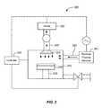
- FIG. 3illustrates a schematic view of a processing apparatus with a remote plasma source.
- FIG. 4presents two micrographs comparing features having oxygen doped silicon carbide produced under similar conditions but employing two different precursors, one containing an alkoxy group and the other without an alkoxy group.
- semiconductor wafersemiconductor wafer
- wafersemiconductor wafer
- substratesubstrate
- wafer substratesemiconductor substrate
- partially fabricated integrated circuitcan refer to a silicon wafer during any of many stages of integrated circuit fabrication thereon.
- a wafer or substrate used in the semiconductor device industrytypically has a diameter of 200 mm, or 300 mm, or 450 mm.
- the following detailed descriptionassumes the invention is implemented on a wafer. However, the invention is not so limited.
- the work piecemay be of various shapes, sizes, and materials.
- other work pieces that may take advantage of this inventioninclude various articles such as printed circuit boards, magnetic recording media, magnetic recording sensors, mirrors, optical elements, micro-mechanical devices and the like.
- Manufacture of semiconductor devicestypically involves depositing one or more thin films on a substrate in an integrated circuit fabrication process.
- classes of thin filmssuch as SiC, SiON, SiONC, and SiCN are deposited using atomic layer deposition (ALD), chemical vapor deposition (CVD), plasma-enhanced chemical vapor deposition (PECVD), or any other suitable deposition method.
- ALDatomic layer deposition
- CVDchemical vapor deposition
- PECVDplasma-enhanced chemical vapor deposition
- silicon carbideincludes doped silicon carbides such as oxygen doped silicon carbide, nitrogen doped silicon carbide, and nitrogen and oxygen doped silicon carbide.
- a doped silicon carbidemay have a wide range of dopant concentrations.
- doped silicon carbideshave at most about 50% atomic of dopant atoms, whether those atoms are oxygen, nitrogen, or atoms of another element.
- the doping levelprovides desired film properties.
- the processcan make SiOC films with about 10-15% atomic carbon and about 40% atomic oxygen.
- the filmcontains about 30-35% atomic carbon and about 25-30% atomic oxygen.
- the silicon carbide film's electrical propertieswill differ. Typically, for good electrical properties, the carbon content is relatively low.
- Precursor molecules for depositing SiCinclude silicon-containing molecules having silicon-hydrogen (Si—H) bonds and/or silicon-silicon (Si—Si) bonds bonds, and silicon-carbon (Si—C) bonds.
- Precursor molecules for depositing SiOCinclude silicon-containing molecules having silicon-hydrogen (Si—H) bonds and/or silicon-silicon (Si—Si) bonds, and silicon-oxygen (Si—O) bonds, and/or silicon-carbon (Si—C) bonds.
- Precursor molecules for depositing SiNCinclude silicon-containing molecules having silicon-hydrogen (Si—H) bonds and/or silicon-silicon (Si—Si) bonds, and silicon-nitrogen (Si—N) bonds, and/or silicon-carbon (Si—C) bonds.
- Precursor molecules for depositing SiONCinclude silicon-containing molecules having silicon-hydrogen (Si—H) bonds, and/or silicon-silicon (Si—Si) bonds, and silicon-nitrogen (Si—N) bonds, silicon-oxygen (Si—O) bonds, and/or silicon-carbon (Si—C) bonds.
- Current PECVD processesmay use in situ plasma processing in which a plasma is provided directly adjacent to a processed substrate.
- PECVDmay break Si—O and/or Si—C bonds in the precursor molecules to produce highly reactive radicals or other fragment types having high sticking coefficients.
- the fragments and resulting silicon carbide filmcan include silicon, carbon, and/or oxygen atoms with bonds that are “dangling,” meaning that silicon, carbon, and/or oxygen atoms have reactive unpaired valence electrons.
- High sticking coefficients of the precursor molecules and their fragmentscan deposit silicon carbide films with poor step coverage, as reactive precursor fragments may disproportionately stick to the upper regions of sidewalls and other structures in recessed features.
- the dangling bondscan produce silanol groups (Si—OH) in a deposited SiOC or SiONC film.
- Si—OHsilanol groups
- the filmsmay have detrimentally high dielectric constants. Film quality may also suffer because the direct plasma conditions tend to extract carbon out of the deposited film.
- the dangling bondscan produce increase silicon-hydrogen bonding (Si—H) in deposited silicon carbide films.
- Broken bonds of Si—Ccan be replaced with Si—H under direct plasma deposition conditions.
- the presence of Si—H bonds in silicon carbide filmscan produce films with poor electrical properties. For example, the presence of Si—H bonds can reduce breakdown voltages and can increase leakage currents because the Si—H bonds provide a leakage path for electrons.
- the dangling bondscan lead to uncontrolled chemical or morphological structures in the silicon carbide films.
- such structuresare dense filaments having low or no porosity, such that the film has an unacceptably high dielectric constant.
- the lack of porositycan be the result of the direct plasma conditions breaking Si—C and/or Si—O bonds in cyclic siloxanes that would otherwise provide porosity in an ultralow-k dielectric material.
- Direct plasma conditions sometimes employed in PECVDcan lead to directionality in the deposition because the energy to break up the precursor molecules can be a low frequency which creates a lot of ion bombardment at the surface.
- the directional depositioncan also lead to deposition of silicon carbide films with poor step coverage.
- a direct plasmais a plasma in which the plasma (electrons and positive ions at an appropriate concentration) reside in close proximity to the substrate surface during deposition, sometimes separated from the substrate surface by only a plasma sheath.
- PECVD processesare sometimes inappropriate for depositing silicon carbide films over exposed copper or other metal surfaces because such processes can oxidize metal.
- the PECVD processmay use oxidants such as oxygen (O 2 ), ozone (O 3 ), carbon dioxide (CO 2 ), or other oxidizing species to form an oxygen doped silicon carbide such as SiOC.
- FIG. 1Aillustrates a cross-section of a structure produced having a silicon carbide film deposited over a substrate.
- the film 101can be formed under process conditions producing a relatively mild environment adjacent to the substrate 100 .
- the substrate 100can be any wafer, semiconductor wafer, partially fabricated integrated circuit, printed circuit board, display screen, or other appropriate work piece.
- the process for depositing the silicon carbide film 101can include one or more silicon-containing precursors having one or more Si—H bonds and/or one or more Si—Si bonds, along with other bonds such as silicon-carbon bonds, silicon-oxygen bonds, and/or silicon-nitrogen bonds, depending on the type of doped structure to be produced.
- the precursorsdo not include oxygen-carbon bonds or nitrogen-carbon bonds.
- the precursorsdo not include alkoxy or amine groups.
- the silicon-containing precursorscan include silicon-oxygen containing precursors, silicon-nitrogen containing precursors, and/or silicon-carbon containing precursors.
- the silicon-oxygen containing precursorscan include one or more Si—O bonds
- the silicon-nitrogen containing precursorscan include one or more Si—N bonds
- the silicon-carbon containing precursorscan include one or more Si—C bonds.
- the silicon-containing precursorscan include a single reactant A with Si—O and Si—C bonds, or Si—N and Si—C bonds.
- the silicon-containing precursorscan include a reactant B with Si—O bonds or Si—N bonds, and a reactant C with Si—C bonds. It will be understood that any number of suitable reactants may be employed in the scope of this present disclosure.
- the chemical structures of exemplary silicon-containing precursorsare discussed in further detail below.
- the silicon-containing precursorsinclude one or more Si—H bonds and/or one or more Si—Si bonds.
- the Si—H bonds and/or Si—Si bondsare broken and serve as reactive sites for forming bonds between the silicon-containing precursors in the deposited silicon carbide film 101 .
- the broken bondscan also serve as sites for cross-linking during thermal processing conducted during or after deposition. Bonding at the reactive sites and cross-linking can form a primary backbone or matrix collectively in the resulting silicon carbide film 101 .
- the process conditionscan substantially preserve Si—C and, if present, Si—O and Si—N bonds in the as-deposited layer of silicon carbide film 101 .
- the reaction conditions adjacent to the substrate 100provide for the breaking of Si—H and/or Si—Si bonds, e.g., extracting hydrogen from the broken Si—H bonds, but the reaction conditions do not provide for extracting oxygen from Si—O bonds, nitrogen from Si—N bonds, or carbon from Si—C bonds.
- the described reaction conditionsexist at the exposed face of the work piece (the face where the silicon carbide film is deposited). They may further exist at some distance above the work piece, e.g., about 0.5 micrometers to about 150 millimeters above the work piece. In effect, activation of the precursor can happen in the gas phase at a substantial distance above the work piece.
- the pertinent reaction conditionswill be uniform or substantially uniform over the entire exposed face of the substrate, although certain applications may permit some variation.
- the environment adjacent the work piececan include one or more radical species, preferably in a substantially low energy state.
- An example of such speciesincludes hydrogen atom radicals.
- all, substantially all, or a substantial fraction of the hydrogen atom radicalscan be in the ground state, e.g., at least about 90% or 95% of the hydrogen atom radicals adjacent the work piece are in the ground state.
- hydrogenis provided in a carrier such helium.
- hydrogen gasmay be provided in a helium carrier at a concentration of about 1-10% hydrogen. Pressure, fraction of carrier gas such as helium, and other process conditions are chosen so that the hydrogen atoms encounter the substrate as radicals in a low energy state without recombining.
- hydrogen gasmay be supplied into a remote plasma source to generate hydrogen radicals.
- the hydrogen radicalsmay be in an excited energy state.
- hydrogen in an excited energy statecan have an energy of at least 10.2 eV (first excited state).
- Excited hydrogen radicalsmay cause unselective decomposition of the silicon-containing precursor.
- hydrogen radicals in an excited statecan easily break Si—H, Si—Si, Si—N, Si—O, and Si—C bonds, which can alter the composition or physical or electrical characteristics of the silicon carbide film.
- the excited hydrogen radicalswhen the excited hydrogen radicals lose their energy, or relax, the excited hydrogen radical may become a substantially low energy state hydrogen radical or a ground state hydrogen radical.
- Hydrogen radicals in a substantially low energy state or ground statecan be capable of selectively breaking Si—H and Si—Si bonds while generally preserving Si—O, Si—N, and Si—C bonds.
- process conditionsmay be provided so that excited hydrogen radicals lose energy or relax to form substantially low energy state or ground state hydrogen radicals.
- the remote plasma source or associated componentsmay be designed so that a residence time of hydrogen radicals diffusing from the remote plasma source to the substrate is greater than the energetic relaxation time of an excited hydrogen radical.
- the energetic relaxation time for an excited hydrogen radicalcan be about equal to or less than 1 ⁇ 10 ⁇ 3 seconds.
- a state in which a substantial fraction of hydrogen atom radicals are in the ground statecan be achieved by various techniques. Some apparatus, such as described below, are designed to achieve this state. Apparatus features and process control features can be tested and tuned to produce a mild state in which a substantial fraction of the hydrogen atom radicals are in the ground state. For example, an apparatus may be operated and tested for charged particles downstream of the plasma source; i.e., near the substrate. The process and apparatus may be tuned until substantially no charged species exist near the substrate. Additionally, apparatus and process features may be tuned to a configuration where they begin to produce a high quality silicon carbide film from a standard precursor such as trimethylsilane. The relatively mild conditions that support such film deposition are chosen.
- radical speciesinclude oxygen-containing species such as elemental oxygen radicals (atomic or biatomic), nitrogen-containing species such as elemental nitrogen radicals (atomic or biatomic), and N—H containing radicals such as ammonia radicals, where nitrogen is optionally incorporated into the film.
- the aforementioned radical speciesmay be produced from a gas that includes hydrogen, nitrogen, N—H containing species, or mixtures thereof.
- essentially all atoms of the deposited filmare provided by the precursor molecules.
- the low energy radicals used to drive the deposition reactionmay be exclusively hydrogen or other species that does not substantially contribute to the mass of the deposited layer.
- the radical speciescan be produced by a remote plasma source.
- radicals of higher energy state or even ionscan potentially be present near the wafer plane.
- the process conditionsemploy radical species in a substantially low energy state sufficient to break Si—H bonds and/or Si—Si bonds while substantially preserving Si—O, Si—N, and Si—C bonds.
- Such process conditionsmay not have substantial amounts of ions, electrons, or radical species in high energy states such as states above the ground state.
- the concentration of ions in the region adjacent the filmis no greater than about 10 7 /cm 3 .
- the presence of substantial amounts of ions or high energy radicalsmay tend to break Si—O, Si—N, and Si—C bonds, which can produce films with undesirable electrical properties (e.g., high dielectric constants and/or low breakdown voltages) and poor conformality. It is believed that an excessively reactive environment produces reactive precursor fragments that have high sticking coefficients (representing a propensity to chemically or physically stick to work piece sidewalls), resulting in poor conformality.
- the silicon-containing precursorsare typically delivered with other species, notably carrier gas, in the environment adjacent to the substrate 100 .
- the silicon-containing precursorsare present with the radical species and other species, including other reactive species and/or carrier gases.
- the silicon-containing precursorsmay be introduced as a mixture. Upstream from the deposition reaction surface, the silicon-containing precursors can be mixed with an inert carrier gas.
- Example inert carrier gasesinclude, but are not limited to, argon (Ar) and helium (He).
- the silicon-containing precursorscan be introduced in a mixture having major and minor species, with the minor species containing some element or structural feature (e.g., a ring structure, a cage structure, an unsaturated bond, etc.) that is present in the silicon carbide film 101 at a relatively low concentration.
- the multiple precursorsmay be present in equimolar or relatively similar proportions as appropriate to form the primary backbone or matrix in the resulting silicon carbide film 101 .
- the relative amounts of the different precursorsare substantially skewed from equimolarity.
- one or more silicon-containing precursorsprovide essentially all of the mass of the deposited silicon carbide film, with small amounts of hydrogen or other element from a remote plasma providing less than about 5% atomic or less than about 2% atomic of the film mass.
- only the radical species and one or more silicon-containing precursorscontribute to the composition of the deposited silicon carbide film.
- the deposition reactionincludes a co-reactant other than one or more silicon-containing precursors and the radical species.
- co-reactantsexamples include carbon dioxide (CO 2 ), carbon monoxide (CO), water (H 2 O), methanol (CH 3 OH), oxygen (O 2 ), ozone (O 3 ), nitrogen (N 2 ), nitrous oxide (N 2 O), ammonia (NH 3 ), methane (CH 4 ), ethane (C 2 H 6 ), acetylene (C 2 H 2 ), ethylene (C 2 H 4 ), diborane, and combinations thereof.
- Such materialsmay be used as nitriding agents, oxidizers, reductants, etc. In some cases, they can be used to tune the amount of carbon in the deposited film by removing a fraction of the carbon provided with the silicon-containing precursor.
- the co-reactantis introduced to the reactor via the same flow path as the silicon-containing precursor; e.g., a path including a showerhead, typically without direct exposure to plasma.
- oxygen and/or carbon dioxideis introduced with the precursor to alter the composition of the silicon carbide film by removing carbon from the film or precursor during deposition.
- the co-reactantis introduced to the reactor via the same flow path as the hydrogen, such that the co-reactant is at least partially converted to radicals and/or ions.
- the hydrogen radicals and the co-reactant radicalsboth react with the silicon-containing precursor(s) to produce the deposited silicon carbide film.
- co-reactantsare used and they are introduced to the chamber with the species being converted to radicals (e.g., hydrogen), they are provided to reactor in relatively small amounts in comparison to the other gases in the reactor, including the source of radicals (e.g., hydrogen) any carrier gas(es) such as helium.
- the co-reactantmay be present in the process gases at about 0.05% or less by mass, or at about 0.01% or less by mass, or at about 0.001% or less by mass.
- a reactant mixture(that goes into the plasma source) may be about 10 L/m He, about 200-500 sccm H2, and about 1-5 sccm oxygen.
- the co-reactantsWhen the co-reactants are introduced to the chamber along with the silicon-containing precursor (e.g., through a showerhead), they may be present at a higher concentration; for example about 2% or less or about 0.1% or less.
- the co-reactantis a relatively weak reactant (e.g., a weak oxidant such as carbon dioxide), it may be present at even higher concentrations, such as about 10% or less or about 4% or less.
- the temperature in the environment adjacent to the substrate 100can be any suitable temperature facilitating the deposition reaction, but sometimes limited by the application of the device containing the silicon carbide film 101 .
- the temperature in the environment adjacent to the substrate 100can be largely controlled by the temperature of a pedestal on which a substrate 100 is supported during deposition of the silicon carbide film 101 .
- the operating temperaturecan be between about 50° C. and about 500° C.
- the operating temperaturecan be between about 200° C. and about 400° C. in many integrated circuit applications.
- increasing the temperaturecan lead to increased cross-linking on the substrate surface.
- the pressure in the environment adjacent to the substrate 100can be any suitable pressure to produce reactive radicals in a process chamber.
- the pressurecan be about 35 Torr or lower.
- the pressurecan be between about 10 Torr and about 20 Torr, such as in embodiments implementing a microwave generated plasma.
- the pressurecan be less than about 10 Torr, or between about 0.2 Torr and about 8 Torr, such as in embodiments implementing a radiofrequency (RF) generated plasma.
- RFradiofrequency
- FIGS. 1B-1Dillustrate cross-sections of structures containing silicon carbide films in a variety of applications.
- FIG. 1Billustrates silicon carbide vertical structures on the sidewalls of a gate electrode structure of a transistor.
- FIG. 1Cillustrates silicon carbide vertical structures on exposed sidewalls of copper lines in an air gap type metallization layer.
- FIG. 1Dillustrates silicon carbide pore sealants for porous dielectric materials.
- the precursors employed in forming silicon carbide filmscan include silicon-containing precursors, with at least some of the silicon-containing precursors having at least one Si—H and/or at least one Si—Si bond.
- the silicon-containing precursorhas at most one hydrogen atom on every silicon atom.
- a precursor having one silicon atomhas at most one hydrogen atom bonded to the silicon atom;
- a precursor having two silicon atomshas one hydrogen atom bonded to one silicon atom and optionally another hydrogen atom bonded to the second silicon atom;
- a precursor having three silicon atomshas at least one hydrogen atom bonded to one silicon atom and optionally one or two more hydrogen atoms bonded to one or two of the remaining silicon atoms, and so on.
- the silicon-containing precursorsmay include at least one Si—O bond, at least one Si—N bond, and/or at least one Si—C bond. While any number of appropriate precursors can be used in forming silicon carbide films, at least some of the precursors will include silicon-containing precursors with at least one Si—H bond or Si—Si bond, and optionally at least one Si—O bond, Si—N bond, and/or Si—C bond.
- the silicon-containing precursor(s)contain no O—C or N—C bonds; e.g., the precursor(s) contain no alkoxy (—O—R), where R is an organic group such as a hydrocarbon group, or amine (—NR 1 R 2 ) groups, wherein R 1 and R 2 are independently hydrogen or organic groups. It is believed that such groups may impart high sticking coefficients to the precursors or fragments on which they reside.
- no precursor or other compound delivered to the substrate during silicon carbide formationcontains an alkoxy or amine group.
- the carbon provided for the silicon carbide filmis provided by one or more hydrocarbon moieties on the silicon-containing precursor.
- Such moietiesmay be from alkyl groups, alkene groups, alkyne groups, aryl groups, and the like.
- the hydrocarbon grouphas a single carbon atom to minimize steric hindrance of the Si—H and/or Si—Si bond breaking reaction during deposition.
- the precursorsare not limited to single-carbon groups; higher numbers of carbon atoms may be used such as 2, 3, 4, 5, or 6 carbon atoms.
- the hydrocarbon groupis linear.
- the hydrocarbon groupis cyclic.
- the silicon-containing precursorsfall into one of three or more chemical classes, any of which may be present alone as the sole precursor or in combination with other types of precursors. It will be understood that other chemical classes of silicon-containing precursors may be employed and that the silicon-containing precursors are not limited to the chemical classes discussed below.
- the silicon-containing precursorcan be a siloxane.
- the siloxanemay be cylic.
- Cyclic siloxanesmay include cyclotetrasiloxanes, such as 2,4,6,8-tetramethylcyclotetrasiloxane (TMCTS) and heptamethylcyclotetrasiloxane (HMCTS).
- Other cyclic siloxanescan also include but are not limited to cyclotrisiloxanes and cyclopentasiloxanes.
- Embodiments using cyclic siloxanesare ring structures that can introduce porosity into a silicon carbide film, with the size of the pores corresponding to the radius of the ring.
- a cyclotetrasiloxane ringcan have a radius of about 6.7 ⁇ .
- the siloxanemay have a three-dimensional or caged structure.
- FIG. 2illustrates examples of representative caged siloxane precursors.
- Caged siloxaneshave silicon atoms bridged to one another via oxygen atoms to form a polyhedron or any 3-D structure.
- An example of a caged siloxane precursor moleculeis silsesquioxane.
- Caged siloxane structuresare described in further detail in commonly owned U.S. Pat. No. 6,576,345 to Cleemput et al., which is incorporated by reference herein for all purposes.
- the caged siloxanecan introduce porosity into a silicon carbide film.
- the porosity scaleis mesoporous.
- the siloxanemay be linear.
- suitable linear siloxanesinclude but are not limited to disiloxanes, such as pentamethyldisiloxane (PMDSO) and tetramethyldisiloxane (TMDSO), and trisiloxanes such as hexamethyltrisiloxane, heptamethyltrisiloxane.
- the silicon-containing precursorcan be an alkyl silane or other hydrocarbon-substituted silane.
- the alkyl silanesinclude a central silicon atom with one or more alkyl groups bonded to it as well as one or more hydrogen atoms bonded to it. In certain embodiments, any one or more of the alkyl groups contain 1-5 carbon atoms.
- the hydrocarabon groupsmay be saturated or unsaturated (e.g., alkene (e.g., vinyl), alkyne, and aromatic groups).
- Examplesinclude but are not limited to trimethylsilane (3MS), triethylsilane, pentamethyl disilamethane ((CH 3 ) 2 Si—CH 2 —Si(CH 3 ) 3 ), and dimethylsilane (2MS).
- one of the silicon atomscan have a carbon-containing or hydrocarbon group attached to it, and one of the silicon atoms can have a hydrogen atom attached to it.
- the silicon-containing precursorcan be a nitrogen-containing compound such as a silicon-nitrogen hydride (e.g., a silazane).
- a nitrogen-containing compoundsuch as a silicon-nitrogen hydride (e.g., a silazane).
- such compoundscontain carbon, but only bonded to silicon atoms, and not to nitrogen atoms.
- the nitrogen-containing compounddoes not have any carbon-nitrogen bonds.
- the nitrogen-containing compounddoes not have any amine moieties (—C—NR 1 R 2 ), where R 1 and R 2 are the same or different groups such hydrogen atoms and hydrocarbon groups such as alkyl groups, alkene groups, or alkyne groups.
- Suitable silicon-nitrogen precursorsinclude various silazanes such as cyclic and linear silazanes containing one or more hydrocarbon moieties bonded to one or more silicon atoms and one or more hydrogen atoms bonded to one or more silicon atoms.
- silazanesinclude methyl-substituted disilazanes and trisilazanes, such as tetramethyldisilazane and hexamethyl trisilazane.
- multiple silicon-containing precursorscan be present in the process gas.
- a siloxane and an alkyl silanemay be used together, or a siloxane and a disilazane may be used together.
- the relative proportions of the individual precursorscan be chosen based on the chemical structures of precursors chosen and the application of the resulting silicon carbide film.
- the amount of siloxanecan be greater than the amount of silane in molar percentages to produce a porous film as discussed in more detail below.
- Suitable precursorsinclude cyclic siloxanes such as cyclotetrasiloxanes such as heptamethylcyclotetrasiloxane (HMCTS) and tetramethylcyclotetrasiloxane.
- cyclic siloxanescan also include but are not limited to cyclotrisiloxanes and cyclopentasiloxanes.
- suitable precursorsinclude linear siloxanes such as, but not limited to, disiloxanes, such as pentamethyldisiloxane (PMDSO), tetramethyldisiloxane (TMDSO), hexamethyl trisiloxane, and heptamethyl trisiloxane.
- PMDSOpentamethyldisiloxane
- TMDSOtetramethyldisiloxane
- hexamethyl trisiloxanehexamethyl trisiloxane
- heptamethyl trisiloxaneheptamethyl trisiloxane
- Suitable precursorsinclude monosilanes substituted with one or more alkyl, alkene, and/or alkyne groups containing, e.g., 1-5 carbon atoms. Examples include but are not limited to trimethylsilane (3MS), dimethylsilane (2MS), triethylsilane (TES), and pentamethyldisilamethane.
- disilanes, trisilanes, or other higher silanesmay be used in place of monosilanes.
- An example of one such disilane from the alkyl silane classis hexamethyldisilane (HMDS).
- HMDShexamethyldisilane
- PMDSpentamethyldisilane
- alkyl silanescan include alkylcarbosilanes, which can have a branched polymeric structure with a carbon bonded to a silicon atom as well as alkyl groups bonded to a silicon atom. Examples include dimethyl trimethylsilyl methane (DTMSM) and bis-dimethylsilyl ethane (BDMSE).
- DTMSMdimethyl trimethylsilyl methane
- BDMSEbis-dimethylsilyl ethane
- suitable precursorsinclude, e.g., alkyldisilazanes and possibly compounds including amino (—NH2) and alkyl groups separately bonded to one or more silicon atoms.
- Alkyldisilazanesinclude silizanes and alkyl groups bonded to two silicon atoms.
- An exampleincludes 1,1,3,3-tetramethyldisilazane (TMDSN).
- silicon-containing precursorsare chosen to provide highly conformal silicon carbide films. It is believed that silicon-containing precursors having low sticking coefficients are capable of producing highly conformal films.
- “Sticking coefficient”is a term used to describe the ratio of the number of adsorbate species (e.g., fragments or molecules) that adsorb/stick to a surface compared to the total number of species that impinge upon that surface during the same period of time.
- S cis sometimes used to refer to the sticking coefficient. The value of S c is between 0 (meaning that none of the species stick) and 1 (meaning that all of the impinging species stick).
- the sticking coefficientincluding the type of impinging species, surface temperature, surface coverage, structural details of the surface, and the kinetic energy of the impinging species. Certain species are inherently more “sticky” than others, making them more likely to adsorb onto a surface each time the specie impinges on the surface. These more sticky species have greater sticking coefficients (all other factors being equal), and are more likely to adsorb near the entrance of a recessed feature compared to less sticky species having lower sticking coefficients. In some cases, the sticking coefficient of the precursors (at the relevant deposition conditions) may be about 0.05 or less, for example about 0.001 or less.
- the deposited filmwill include silicon, carbon, and in some cases oxygen, nitrogen, and/or one or more other elements.
- the atomic concentration of siliconis between about 15% and 45% (or about 25% to 40%)
- the atomic concentration of carbonis between about 10% and 50%
- the atomic concentration of oxygenis between about 0% and 45%
- the atomic concentration of nitrogenis between about 0% and 45%.
- the atomic concentration of siliconis about 30%
- the atomic concentration of oxygenis about 25%
- the atomic concentration of carbonis about 45%.
- the atomic concentration of siliconis about 30%, the atomic concentration of oxygen is about 45%, and the atomic concentration of carbon is about 25%.
- the filmcontains about 10-15% carbon and about 30-40% oxygen, both on an atomic basis. In all cases, the film contains some hydrogen. It will be understood that the relative atomic concentrations can vary depending on the choice of the precursor.
- the silicon atomswill form bonds with carbon and optionally nitrogen and/or oxygen atoms.
- the deposited filmcontains more Si—O bonds than Si—C bonds. This can provide a relatively porous film with a lower dielectric constant.
- the deposited filmcontains a ratio of Si—O bonds to Si—C bonds that is between about 0.5:1 and 3:1.
- the deposited filmcontains more Si—N bonds than Si—C bonds.
- the deposited filmcontains a ratio of Si—N bonds to Si—C bonds that is between about 0.5:1 and 3:1.
- the film densityis between about 2 and 2.7 g/cm 3 .
- the internal structure of the precursoris maintained in the deposited film. This structure may preserve all or most of the Si—C, and Si—O and/or Si—N bonds, if present, in the precursor, while linking or cross-linking individual precursor moieties through bonds at locations where Si—H bonds and/or Si—Si bonds existed in the precursor molecules and/or through additional condensation reactions on the growing surface if sufficient thermal energy is provided.
- the process conditions described earlier hereincan provide a film structure that is highly conformal.
- the relatively mild process conditionscan minimize the degree of ion bombardment at the surface of the substrate so that the deposition lacks directionality.
- the relatively mild process conditionscan reduce the number of radicals with high sticking coefficients that would have a tendency to stick to the sidewalls of previously deposited layers or films.
- the silicon carbide filmmay be deposited with a conformality of between about 25% and 100%, more typically between about 50% and 100%, and even more typically between about 80% and 100%.
- Conformalitymay be calculated by comparing the average thickness of a deposited film on a bottom, sidewall, or top of a feature to the average thickness of a deposited film on a bottom, sidewall, or top of a feature. For example, conformality may be calculated by dividing the average thickness of the deposited film on the sidewall by the average thickness of the deposited film at the top of the feature and multiplying it by 100 to obtain a percentage. For certain applications, a conformality of between about 85% and 95% is sufficient. In some examples depositing silicon carbide on features having an aspect ratio of between about 2:1 and about 4:1, the conformality is at least about 90%. Certain BEOL (back end of line) processes fall into this category.
- the conformalityis at least about 80%.
- Certain spacer deposition processesfall into this category.
- depositing silicon carbide on features having an aspect ratio of between about 7:1 and about 10:1 (and even higher)the conformality is at least about 90%.
- Certain DRAM (dynamic random access memory) fabrication processesfall into this category.
- the process conditionscan also provide a film structure with a high breakdown voltage and a low leakage current.
- a limited amount of oxygen or nitrogeninto a SiC class of material, leakage paths provided by Si—H bonds and/or Si—CH 2 —Si bonds may be blocked by oxygen or nitrogen.
- the mode of conductionmay be different in Si—O and Si—N at low fields. This can provide improved electrical properties while maintaining a relatively low dielectric constant.
- the filmhas an effective dielectric constant of about 5 or lower, or about 4.0 or lower, and in some cases about 3.5 or lower, and some cases about 3.0 or lower, and in still other implementations about 2.5 or lower.
- the effective dielectric constantcan depend on the bonding and density.
- SiOC filmsare made with a dielectric constant of 6 or greater, particularly when the carbon content is relatively high. If leakage current is an important consideration, SiOC needs to be ⁇ 5. The lower you go, the worse will be its hermetic and barrier and thermal resistance properties.
- the silicon carbide filmmay be made dense and highly cross-linked. This can be accomplished by, for example, a) depositing the film at a relatively high temperature, and/or b) providing a relatively high radicals:precursor ratio.
- the silicon carbide filmcan be relatively thin and yet serve as an effective hermetic or diffusion barrier.
- the deposited filmcan be porous.
- the silicon-containing precursorscan include cyclic siloxanes and caged siloxanes. These precursors, and others that have significant interior open space, can introduce significant porosity into the structure of the deposited film. Porosity in the deposited film can further lower the dielectric constant. In some embodiments, the porosity of the deposited silicon carbide film is between about 20% and 50%.
- the pore size of porous filmmay track that of the cyclic or caged precursor. In certain embodiments, the film's average pore size is between about 5 ⁇ and 20 ⁇ , such as about 16 ⁇ .
- a suitable apparatusincludes hardware for accomplishing the process operations and a system controller having instructions for controlling process operations in accordance with the present disclosure.
- the apparatus for performing the aforementioned process operationscan include a remote plasma source.
- a remote plasma sourceprovides mild reaction conditions in comparison to a direct plasma.
- An example of a suitable remote plasma apparatusis described in U.S. patent application Ser. No. 14/062,648, filed Oct. 24, 2013, which is incorporated herein by reference in its entirety.
- FIG. 3presents a schematic diagram of a remote plasma apparatus according to certain embodiments.
- the device 300includes a reaction chamber 310 with a showerhead assembly 320 . Inside the reaction chamber 310 , a substrate 330 rests on a stage or pedestal 335 . In some embodiments, the pedestal 335 can be fitted with a heating/cooling element.
- a controller 340may be connected to the components of the device 300 to control the operation of the device 300 .
- the controller 340may contain instructions or controlling process conditions for the operations of the device 300 , such as the temperature process conditions and/or the pressure process conditions.
- gases or gas mixturesare introduced into the reaction chamber 310 via one or more gas inlets coupled to the reaction chamber 310 .
- two or more gas inletsare coupled to the reaction chamber 310 .
- a first gas inlet 355can be coupled to the reaction chamber 310 and connected to a vessel 350
- a second gas inlet 365can be coupled to the reaction chamber 310 and connected to a remote plasma source 360 .
- the delivery lines for the precursors and the radical species generated in the remote plasma sourceare separated. Hence, the precursors and the radical species do not substantially interact before reaching the substrate 330 .
- One or more radical speciesmay be generated in the remote plasma source 360 and configured to enter the reaction chamber 310 via the gas inlet 365 .
- Any type of plasma sourcemay be used in remote plasma source 360 to create the radical species. This includes, but is not limited to, capacitively coupled plasmas, inductively coupled plasmas, microwave plasmas, DC plasmas, and laser-created plasmas.
- An example of a capacitively coupled plasmacan be a radio frequency (RF) plasma.
- RFradio frequency
- a high-frequency plasmacan be configured to operate at 13.56 MHz or higher.
- An example of such a remote plasma source 360can be the GAMMA®, manufactured by Novellus Systems of San Jose, Calif.
- a RF remote plasma source 360can be the Astron®, manufactured by MKS Instruments of Wilmington, Mass., which can be operated at 440 kHz and can be provided as a subunit bolted onto a larger apparatus for processing one or more substrates in parallel.
- a microwave plasmacan be used as the remote plasma source 360 , such as the Astex®, also manufactured by MKS Instruments.
- a microwave plasmacan be configured to operate at a frequency of 2.45 GHz.
- Gas provided to the remote plasma sourcemay include hydrogen, nitrogen, oxygen, and other gases as mentioned elsewhere herein.
- hydrogenis provided in a carrier such helium.
- hydrogen gasmay be provided in a helium carrier at a concentration of about 1-10% hydrogen.
- the precursorscan be provided in vessel 350 and can be supplied to the showerhead 320 via the first gas inlet 355 .
- the showerhead 320distributes the precursors into the reaction chamber 310 toward the substrate 330 .
- the substrate 330can be located beneath the showerhead 320 . It will be appreciated that the showerhead 320 can have any suitable shape, and may have any number and arrangement of ports for distributing gases to the substrate 330 .
- the precursorscan be supplied to the showerhead 320 and ultimately to the substrate 330 at a controlled flow rate.
- the one or more radical species formed in the remote plasma source 360can be carried in the gas phase toward the substrate 330 .
- the one or more radical speciescan flow through a second gas inlet 365 into the reaction chamber 310 .
- the second gas inlet 365need not be transverse to the surface of the substrate 330 as illustrated in FIG. 3 .
- the second gas inlet 365can be directly above the substrate 330 or in other locations.
- the distance between the remote plasma source 360 and the reaction chamber 310can be configured to provide mild reactive conditions such that the ionized species generated in the remote plasma source 360 are substantially neutralized, but at least some radical species in substantially low energy states remain in the environment adjacent to the substrate 330 .
- the distance between the remote plasma source 360 and the reaction chamber 310can be a function of the aggressiveness of the plasma (e.g., determined in part by the source RF power level), the density of gas in the plasma (e.g., if there's a high concentration of hydrogen atoms, a significant fraction of them may recombine to form H 2 before reaching the reaction chamber 310 ), and other factors.
- the distance between the remote plasma source 360 and the reaction chamber 310can be between about 1 cm and 30 cm, such as about 5 cm or about 15 cm.
- a co-reactantwhich is not the primary silicon-containing precursor or a hydrogen radical, may be introduced during the deposition reaction.
- the apparatusis configured to introduce the co-reactant through the second gas inlet 365 , in which case the co-reactant is at least partially converted to plasma.
- the apparatusis configured to introduce the co-reactant through the showerhead 320 via the first gas inlet 355 .
- the co-reactantinclude oxygen, nitrogen, carbon dioxide, and the like.
- the controller 340may contain instructions for controlling process conditions for the operation of the device 300 .
- the controller 340will typically include one or more memory devices and one or more processors.
- the processormay include a CPU or computer, analog and/or digital input/output connections, stepper motor controller boards, etc. Instructions for implementing appropriate control operations are executed on the processor. These instructions may be stored on the memory devices associated with the controller 340 or they may be provided over a network.
- the controller 340controls all or most activities of the semiconductor processing device 300 described herein.
- the controller 340may control all or most activities of the semiconductor processing device 300 associated with depositing a silicon carbide film and, optionally, other operations in a fabrication flow that includes the silicon carbide films.
- the controller 340may execute system control software including sets of instructions for controlling the timing, gas composition, gas flow rates, chamber pressure, chamber temperature, RF power levels, substrate position, and/or other parameters.
- Other computer programs, scripts, or routines stored on memory devices associated with the controller 340may be employed in some embodiments.
- controller 340may adjust the substrate position to further reduce the presence of high-energy radical species at the environment adjacent to the substrate 330 .
- the controller 340may comprise different or identical instructions for different apparatus stations, thus allowing the apparatus stations to operate either independently or synchronously.
- the controller 340may include instructions for performing operations such as flowing a silicon-containing precursor through the first gas inlet 355 into the reaction chamber 310 , providing the one or more radical species in a substantially low energy state from the remote plasma source 360 , and flowing the one or more radical species through the second gas inlet 365 into the reaction chamber 310 to react with the silicon-containing precursor to form the silicon carbide film on the substrate 330 .
- the apparatusmay include a user interface associated with controller 340 .
- the user interfacemay include a display screen, graphical software displays of the apparatus and/or process conditions, and user input devices such as pointing devices, keyboards, touch screens, microphones, etc.
- the computer program code for controlling the above operationscan be written in any conventional computer readable programming language: for example, assembly language, C, C++, Pascal, Fortran, or others. Compiled object code or script is executed by the processor to perform the tasks identified in the program.
- Signals for monitoring the processmay be provided by analog and/or digital input connections of the system controller.
- the signals for controlling the processare output on the analog and digital output connections of the processing system.
- the methods described hereincan be performed on systems including semiconductor processing equipment such as a processing tool or tools, chamber or chambers, a platform or platforms for processing, and/or specific processing components (a wafer pedestal, a gas flow system, etc.). These systems may be integrated with electronics for controlling their operation before, during, and after processing of a semiconductor wafer or substrate. In general, the electronics are referred to as the controller, which may control various components or subparts of the system or systems.
- the controllermay be programmed to control any of the processes disclosed herein, including the delivery of processing gases, temperature settings (e.g., heating and/or cooling), pressure settings, vacuum settings, power settings, radio frequency (RF) generator settings, RF matching circuit settings, frequency settings, flow rate settings, fluid delivery settings, positional and operation settings, wafer transfers into and out of a tool and other transfer tools and/or load locks connected to or interfaced with a specific system.
- temperature settingse.g., heating and/or cooling
- RFradio frequency
- the controllermay be defined as electronics having various integrated circuits, logic, memory, and/or software that receive instructions, issue instructions, control operation, enable cleaning operations, enable endpoint measurements, and the like.
- the integrated circuitsmay include chips in the form of firmware that store program instructions, digital signal processors (DSPs), chips defined as application specific integrated circuits (ASICs), and/or one or more microprocessors, or microcontrollers that execute program instructions (e.g., software).
- Program instructionsmay be instructions communicated to the controller in the form of various individual settings (or program files), defining operational parameters for carrying out a particular process on or for a semiconductor wafer or to a system.
- the operational parametersmay, in some embodiments, be part of a recipe defined by process engineers to accomplish one or more processing steps during the fabrication of one or more layers, materials (e.g., silicon carbide), surfaces, circuits, and/or dies of a wafer.
- the controllermay be a part of or coupled to a computer that is integrated with, coupled to the system, otherwise networked to the system, or a combination thereof.
- the controllermay be in the “cloud” or all or a part of a fab host computer system, which can allow for remote access of the wafer processing.
- the computermay enable remote access to the system to monitor current progress of fabrication operations, examine a history of past fabrication operations, examine trends or performance metrics from a plurality of fabrication operations, to change parameters of current processing, to set processing steps to follow a current processing, or to start a new process.
- a remote computere.g. a server
- the remote computermay include a user interface that enables entry or programming of parameters and/or settings, which are then communicated to the system from the remote computer.
- the controllerreceives instructions in the form of data, which specify parameters for each of the processing steps to be performed during one or more operations. It should be understood that the parameters may be specific to the type of process to be performed and the type of tool that the controller is configured to interface with or control.
- the controllermay be distributed, such as by comprising one or more discrete controllers that are networked together and working towards a common purpose, such as the processes and controls described herein.
- An example of a distributed controller for such purposeswould be one or more integrated circuits on a chamber in communication with one or more integrated circuits located remotely (such as at the platform level or as part of a remote computer) that combine to control a process on the chamber.
- example systemsmay include a plasma etch chamber or module, a deposition chamber or module, a spin-rinse chamber or module, a metal plating chamber or module, a clean chamber or module, a bevel edge etch chamber or module, a physical vapor deposition (PVD) chamber or module, a chemical vapor deposition (CVD) chamber or module, an atomic layer deposition (ALD) chamber or module, an atomic layer etch (ALE) chamber or module, an ion implantation chamber or module, a track chamber or module, and any other semiconductor processing systems that may be associated or used in the fabrication and/or manufacturing of semiconductor wafers.
- PVDphysical vapor deposition
- CVDchemical vapor deposition
- ALDatomic layer deposition
- ALEatomic layer etch
- the controllermight communicate with one or more of other tool circuits or modules, other tool components, cluster tools, other tool interfaces, adjacent tools, neighboring tools, tools located throughout a factory, a main computer, another controller, or tools used in material transport that bring containers of wafers to and from tool locations and/or load ports in a semiconductor manufacturing factory.
- a silicon carbide filmmay be deposited over exposed copper.
- reaction conditions adjacent to the substratecan be free of oxidants, such as O 2 , O 3 , and CO 2 , including radicals thereof.
- the silicon carbide filmmay be deposited directly over the exposed copper without oxidizing copper (e.g., creating cupric oxide).
- Such filmscan serve as etch stop layers, which can also serve as copper diffusion barriers.
- the presence of the silicon carbide filmcan provide a sufficiently low dielectric constant with excellent leakage properties to serve as a diffusion barrier.
- the silicon carbide filmcan be an etch stop and/or diffusion barrier either by itself or as a bilayer stack (e.g., silicon carbide/SiNC bilayer deposited over exposed copper).
- the silicon carbide filmcan be placed in between adjacent metallization layers that are typically produced by a damascene process.
- the silicon carbide filmcan resist etching and can be sufficiently dense to minimize the diffusion of copper ions into adjacent regions of dielectric material.
- the precursor employed for the silicon carbide filmcan be non-cyclic.
- Non-cyclic precursorscan include PMDSO or TMDSO.
- the non-cyclic precursorcan provide a sufficiently high density to serve as a hermetic or diffusion barrier.
- nitrogenmay be incorporated into the film by employing nitrogen-containing precursors or plasma activating nitrogen-containing radicals, such as elemental nitrogen radicals or amine radicals.
- a silicon carbide filmmay be deposited as vertical structures adjacent to metal or semiconductor structures. Deposition of silicon carbide provides excellent step coverage along sidewalls of the metal or semiconductor structures to create the vertical structures. In certain embodiments, the vertical structures may be referred to as spacers or liners.
- FIG. 1Billustrates a cross-section of silicon carbide liners deposited on the sidewalls of a gate electrode structure of a transistor. As illustrated in FIG. 1B , the transistor can be a CMOS transistor with a silicon substrate 110 having a source 112 and a drain 113 . A gate dielectric 114 can be deposited over the silicon substrate 110 , and a gate electrode can be deposited over the gate dielectric 115 to form the transistor.
- Silicon carbide liners 111can be deposited on the sidewalls of the gate electrode 115 and gate dielectric 114 .
- FIG. 1Cillustrates a cross-section of silicon carbide deposited on sidewalls of exposed copper lines in an air gap type metallization layer.
- Air gaps 120can be introduced into an integrated circuit layer between copper lines 122 that can reduce the effective k-value of the layer.
- Silicon carbide liners 121can be deposited on the sidewalls of the copper lines 122 , and a nonconformal dielectric layer 123 can be deposited the air gaps 120 , liners 121 , and copper lines 122 . Examples of such air gap type metallization layers can be described in U.S. Patent Publication No. 2004/0232552 to Fei Wang et al., which is herein incorporated by reference.
- a silicon carbide filmmay be deposited on the sidewalls of patterned porous dielectric materials.
- Ultra low-k dielectric materialscan be made from a porous structure. The pores in such materials can provide areas for ingress of metal during deposition of subsequent layers, including the deposition of diffusion barriers containing a metal such as tantalum (Ta). If too much metal migrates into the dielectric material, the dielectric material may provide a short circuit between adjacent copper metallization lines.
- FIG. 1Dillustrates a cross-section of silicon carbide as a pore sealant for porous dielectric materials.
- a porous dielectric layer 132can have a plurality of trenches or vias cut into the porous dielectric layer 132 to form pores 130 .
- Silicon carbide 131can be deposited along the pores 130 to effectively seal the pores 130 . Sealing the pores 130 with the silicon carbide 131 can avoid damaging the porous dielectric layer 132 that may otherwise be incurred by other sealing techniques using a plasma.
- the silicon carbide 131can be sufficiently dense as a pore sealant and may include non-cyclic silicon-containing precursors, such as PMDSO and TMDSO.
- an etched dielectric materialsuch as the porous dielectric layer 132 may first be treated by a “k-recovery” process, which exposes the porous dielectric layer 132 to UV radiation and a reducing agent. This recovery process is further described in commonly owned U.S. Patent Publication No.
- the porous dielectric layer 132can be exposed to UV radiation and a chemical silylating agent. This recovery process is further described in commonly owned U.S. Patent Publication No. 2011/0117678 to Varadarajan et al., which is incorporated by reference herein for all purposes.
- a layer of conformally deposited silicon carbide 131can be deposited to effectively seal the pores of the porous dielectric layer 132 .
- a silicon carbide filmmay be deposited as an ultra low-k dielectric material itself.
- Ultra low-k dielectricsare conventionally defined as those materials that have a dielectric constant lower than that of 2.5.
- the ultra low-k dielectric material of silicon carbidecan be a porous dielectric layer.
- the pores of the dielectric layercan be introduced by using cyclic or caged precursor molecules, including the cyclic siloxanes and silsesquioxanes.
- the porosity of the ultra low-k dielectric layer of silicon carbidecan be between about 20% and 50%.
- the ultra low-k dielectric layercan have an average pore size of less than about 100 ⁇ , such as between about 5 ⁇ and 20 ⁇ .
- a cyclosiloxane ringcan have a radius of about 6.7 ⁇ . While increasing the number and size of the pores can lower the dielectric constant, the mechanical integrity of the dielectric layer can be compromised if it is too porous.
- FIG. 4presents a scanning electron micrograph of two oxygen doped silicon carbide films: the one on the left was deposited using a precursor with an alkoxy group and the one on the right was deposited using a similar precursor, but without an alkoxy group. Other than the precursor differences, the apparatus and deposition conditions were identical.
- the feature on which the films were depositedhad an aspect ratio of 7:1 and a width of about 60 nm. As shown, the conformality of the film produced using the alkoxy-containing precursor was about 55% and the film produced using the alkoxy-free precursor was about 75%.
Landscapes
- Engineering & Computer Science (AREA)
- Chemical & Material Sciences (AREA)
- Physics & Mathematics (AREA)
- General Physics & Mathematics (AREA)
- Power Engineering (AREA)
- Microelectronics & Electronic Packaging (AREA)
- Computer Hardware Design (AREA)
- Manufacturing & Machinery (AREA)
- Condensed Matter Physics & Semiconductors (AREA)
- Chemical Kinetics & Catalysis (AREA)
- Mechanical Engineering (AREA)
- Organic Chemistry (AREA)
- Metallurgy (AREA)
- Materials Engineering (AREA)
- General Chemical & Material Sciences (AREA)
- Plasma & Fusion (AREA)
- Spectroscopy & Molecular Physics (AREA)
- Inorganic Chemistry (AREA)
- Chemical Vapour Deposition (AREA)
- Formation Of Insulating Films (AREA)
- Internal Circuitry In Semiconductor Integrated Circuit Devices (AREA)
Abstract
Description
- This application is a continuation in part of U.S. patent application Ser. No. 13/494,836, filed Jun. 12, 2012 [Attorney docket no. NOVLP466], and is also a continuation in part of U.S. patent application Ser. No. 13/907,699, filed May 31, 2013 [Attorney docket no. LAMRP046], both of which are incorporated herein by reference in their entireties.
- 1. Field
- The present disclosure relates generally to the formation of silicon carbide films.
- 2. Background
- The silicon carbide (SiC) class of thin films has unique physical, chemical, and mechanical properties and is used in a variety of applications, particularly integrated circuit applications. Classes of SiC thin films include oxygen doped SiC, also known as silicon oxycarbide (SiOC), nitrogen doped SiC, also known as silicon nitricarbide (SiNC), oxygen and nitrogen doped SiC, also known as silicon oxynitricarbide (SiONC), and undoped silicon carbide.
- Provided are methods and systems for preparing silicon carbide. A substantially conformal layer of silicon carbide can be provided using a process employing silicon-containing precursors that have one or more silicon-hydrogen bonds and/or silicon-silicon bonds. The silicon-containing precursors may also have one or more silicon-oxygen bonds, silicon-nitrogen bonds, and/or silicon-carbon bonds. A precursor can be made reactive by breaking the silicon-hydrogen bond(s), e.g., stripping a hydrogen atom from the precursor, or breaking the silicon-silicon bond(s) if present in the precursor, while preserving one or more of the silicon-oxygen bonds, silicon-nitrogen bonds, and/or silicon-carbon bonds in the precursor. The resulting film may contain the one or more silicon-oxygen and/or silicon-carbon bonds. The precursor may be converted to a reactive but substantially intact form by converting it to a radical or other reactive species in which a hydrogen atom or other atom is extracted. The hydrogen or other atom may be extracted by, for example, exposing the precursor to a radical species. In certain embodiments, one or more radical species in a substantially low energy state can react with the silicon-containing precursor(s) to form the silicon carbide. The one or more radical species can be formed in a remote plasma source. The silicon carbide can be used in a wide variety of applications, including but not limited to serving as liners, spacers, etch stops, copper diffusion barriers, pore sealants, and ultra low-k dielectric layers.
- Certain aspects of the disclosure pertain to a method of depositing a silicon carbide film on a substrate, which method may be characterized by the following operations: (a) providing the substrate to a reaction chamber; (b) providing a silicon-containing precursor to the substrate, wherein the silicon-containing precursor has (i) one or more silicon-hydrogen bonds and/or silicon-silicon bonds, (ii) no carbon-oxygen bonds, and (iii) no carbon-nitrogen bonds; and (c) introducing from a source gas one or more radical species in a substantially low energy state to react with the silicon-containing precursor to form the silicon carbide film on the substrate under conditions that break the silicon-containing precursor's silicon-hydrogen bonds or silicon-silicon bonds but substantially preserve the silicon-containing precursor's silicon-carbon bonds. As examples, the silicon carbide film may include an oxygen doped silicon carbide, a nitrogen doped silicon carbide, or an undoped silicon carbide.
- In some cases, the silicon containing precursor has no alkoxy groups (—C—O—R), where R is an organic moiety, and no amine groups (—C—NR1R2), where R1and R2are each independently hydrogen or an organic moiety. In certain implementations, during (b) and (c), no compound containing a carbon-oxygen bond or a carbon-nitrogen bond is provided to the substrate. Further, in certain implementations, the silicon carbide film is formed without performing atomic layer deposition.
- In certain embodiments, the silicon-containing precursor is a cyclic siloxane such as heptamethylcyclotetrasiloxane and tetramethylcyclotetrasiloxane. In certain embodiments, the silicon containing precursor is a linear siloxane such as disiloxane or a trisiloxane. In certain embodiments, the silicon-containing precursor is an alkyl silane such as a disilane or a trisilane. In certain embodiments, the silicon-containing precursor is a silazane.
- In certain embodiments, the radical species contains hydrogen radicals, oxygen radical, and/or nitrogen radicals. In some implementations, introducing the one or more radical species involves exposing the source gas to a remote plasma, which may be produced from an RF power source or a microwave power source.
- In certain embodiments, the ratio of silicon-oxygen or silicon-nitrogen bonds to silicon-carbon bonds in the silicon carbide film is between about 3:1 and about 0.5:1. In some cases, the silicon carbide film on the substrate has a conformality of at least about 90%. In some applications, the substrate contains a transistor having a gate electrode, the method further comprising forming the silicon carbide film on one or more sidewalls of the gate electrode. In some applications, the silicon carbide film comprises an ultralow-k dielectric thin film.
- Certain aspects of the disclosure pertain to an apparatus for depositing a silicon carbide film on a substrate, which apparatus may be characterized by the following features: a reaction chamber configured to hold the substrate during silicon carbide film deposition; a plasma chamber coupled to the reaction chamber and configured to generate a plasma outside the reaction chamber; two or more gas inlets coupled to the reaction chamber; and a controller. The controller may contain instructions for performing the following operations: (a) flowing a silicon-containing precursor through one of the gas inlets into the reaction chamber, wherein the silicon-containing precursor has (i) one or more silicon-hydrogen bonds and/or silicon-silicon bonds, (ii) no carbon-oxygen bonds, and (iii) no carbon-nitrogen bonds; (b) providing one or more radical species in a substantially low energy state from the plasma in the plasma chamber; and (c) flowing the one or more radical species through another one of the gas inlets into the reaction chamber to react with the silicon-containing precursor to form the silicon carbide film on the substrate.
- In some designs, the apparatus has a distance between the reaction chamber and the plasma chamber is between about 1 cm and about 30 cm. In various implementations, the plasma chamber has an RF power source or microwave power source.
- In certain embodiments, the controller further includes instructions for providing no compound containing a carbon-oxygen bond or a carbon-nitrogen bond during (a) through (c).
- In certain embodiments, the controller instructions do not contain instructions for depositing the silicon carbide film using atomic layer deposition.
- In some implementations, the silicon containing precursor has no alkoxy groups (—C—O—R), where R is an organic moiety, and no amine groups (—C—NR1R2), where R1and R2are each independently hydrogen or an organic moiety. In some applications, the silicon-containing precursor is a siloxane. In some implementations, the silicon-containing precursor is an alkyl silane. In some implementations, the silicon-containing precursor is a silazane.
- In some apparatus, the one or more radical species are produced from a gas selected from the group consisting of hydrogen, nitrogen, and ammonia. As an example, the one or more radical species is hydrogen atoms. In some applications, the ratio of silicon-oxygen bonds or silicon-nitrogen bonds to silicon-carbon bonds in the silicon carbide film is between about 3:1 and about 0.5:1. In some applications, the silicon carbide film is an ultralow-k dielectric thin film.
- In certain embodiments, the controller is configured to maintain the reaction chamber at a temperature between about 250° C. and about 400° C. In certain embodiments, the controller is configured to maintain the reaction chamber at a pressure between about 0.2 Torr and about 40 Torr.
- These and other embodiments are described further below with reference to the figures.
FIG. 1A illustrates a cross-section of an example of an SiC film deposited over a substrate.FIG. 1B illustrates SiC vertical structures on the sidewalls of a gate electrode structure of a transistor.FIG. 1C illustrates SiC vertical structures on exposed sidewalls of copper lines in an air gap type metallization layer.FIG. 1D illustrates SiC pore sealants for porous dielectric materials.FIG. 2 illustrates examples of representative caged siloxane precursors.FIG. 3 illustrates a schematic view of a processing apparatus with a remote plasma source.FIG. 4 presents two micrographs comparing features having oxygen doped silicon carbide produced under similar conditions but employing two different precursors, one containing an alkoxy group and the other without an alkoxy group.- The following disclosure presents various details to help explain relevant concepts, which may be practiced without some or all of these details. While some concepts will be described in conjunction with the specific embodiments, it will be understood that these embodiments are not intended to be limiting. In some instances, well known process operations, structures, and other features are not described in detail in order to facilitate understanding the described concepts.
- In this application, the terms “semiconductor wafer,” “wafer,” “substrate,” “wafer substrate,” and “partially fabricated integrated circuit” are used interchangeably. One of ordinary skill in the art would understand that the term “partially fabricated integrated circuit” can refer to a silicon wafer during any of many stages of integrated circuit fabrication thereon. A wafer or substrate used in the semiconductor device industry typically has a diameter of 200 mm, or 300 mm, or 450 mm. The following detailed description assumes the invention is implemented on a wafer. However, the invention is not so limited. The work piece may be of various shapes, sizes, and materials. In addition to semiconductor wafers, other work pieces that may take advantage of this invention include various articles such as printed circuit boards, magnetic recording media, magnetic recording sensors, mirrors, optical elements, micro-mechanical devices and the like.
- Manufacture of semiconductor devices typically involves depositing one or more thin films on a substrate in an integrated circuit fabrication process. In some aspects of the fabrication process, classes of thin films such as SiC, SiON, SiONC, and SiCN are deposited using atomic layer deposition (ALD), chemical vapor deposition (CVD), plasma-enhanced chemical vapor deposition (PECVD), or any other suitable deposition method. As used herein, the term silicon carbide includes doped silicon carbides such as oxygen doped silicon carbide, nitrogen doped silicon carbide, and nitrogen and oxygen doped silicon carbide. A doped silicon carbide may have a wide range of dopant concentrations. For many, doped silicon carbides have at most about 50% atomic of dopant atoms, whether those atoms are oxygen, nitrogen, or atoms of another element. The doping level provides desired film properties. In one example, the process can make SiOC films with about 10-15% atomic carbon and about 40% atomic oxygen. In another example, the film contains about 30-35% atomic carbon and about 25-30% atomic oxygen. Of course, the silicon carbide film's electrical properties will differ. Typically, for good electrical properties, the carbon content is relatively low.
- Precursor molecules for depositing SiC include silicon-containing molecules having silicon-hydrogen (Si—H) bonds and/or silicon-silicon (Si—Si) bonds bonds, and silicon-carbon (Si—C) bonds. Precursor molecules for depositing SiOC include silicon-containing molecules having silicon-hydrogen (Si—H) bonds and/or silicon-silicon (Si—Si) bonds, and silicon-oxygen (Si—O) bonds, and/or silicon-carbon (Si—C) bonds. Precursor molecules for depositing SiNC include silicon-containing molecules having silicon-hydrogen (Si—H) bonds and/or silicon-silicon (Si—Si) bonds, and silicon-nitrogen (Si—N) bonds, and/or silicon-carbon (Si—C) bonds. Precursor molecules for depositing SiONC include silicon-containing molecules having silicon-hydrogen (Si—H) bonds, and/or silicon-silicon (Si—Si) bonds, and silicon-nitrogen (Si—N) bonds, silicon-oxygen (Si—O) bonds, and/or silicon-carbon (Si—C) bonds. Current PECVD processes may use in situ plasma processing in which a plasma is provided directly adjacent to a processed substrate.
- It has been found that depositing high-quality silicon carbide thin films can have certain challenges such as providing films with excellent step coverage, low dielectric constants, high breakdown voltages, low leakage currents, high porosity, and/or coverage over exposed metal surfaces without oxidizing the metal surfaces.
- While this disclosure is not limited by any particular theory, it is believed that the plasma conditions in typical PECVD processes fragment the silicon-containing precursor molecules in a manner that produces undesirable effects. For example, PECVD may break Si—O and/or Si—C bonds in the precursor molecules to produce highly reactive radicals or other fragment types having high sticking coefficients. The fragments and resulting silicon carbide film can include silicon, carbon, and/or oxygen atoms with bonds that are “dangling,” meaning that silicon, carbon, and/or oxygen atoms have reactive unpaired valence electrons. High sticking coefficients of the precursor molecules and their fragments can deposit silicon carbide films with poor step coverage, as reactive precursor fragments may disproportionately stick to the upper regions of sidewalls and other structures in recessed features.
- The dangling bonds can produce silanol groups (Si—OH) in a deposited SiOC or SiONC film. As a result, the films may have detrimentally high dielectric constants. Film quality may also suffer because the direct plasma conditions tend to extract carbon out of the deposited film.
- Furthermore, the dangling bonds can produce increase silicon-hydrogen bonding (Si—H) in deposited silicon carbide films. Broken bonds of Si—C can be replaced with Si—H under direct plasma deposition conditions. The presence of Si—H bonds in silicon carbide films can produce films with poor electrical properties. For example, the presence of Si—H bonds can reduce breakdown voltages and can increase leakage currents because the Si—H bonds provide a leakage path for electrons.
- Further, the dangling bonds can lead to uncontrolled chemical or morphological structures in the silicon carbide films. In some cases, such structures are dense filaments having low or no porosity, such that the film has an unacceptably high dielectric constant. The lack of porosity can be the result of the direct plasma conditions breaking Si—C and/or Si—O bonds in cyclic siloxanes that would otherwise provide porosity in an ultralow-k dielectric material.
- Direct plasma conditions sometimes employed in PECVD can lead to directionality in the deposition because the energy to break up the precursor molecules can be a low frequency which creates a lot of ion bombardment at the surface. The directional deposition can also lead to deposition of silicon carbide films with poor step coverage. A direct plasma is a plasma in which the plasma (electrons and positive ions at an appropriate concentration) reside in close proximity to the substrate surface during deposition, sometimes separated from the substrate surface by only a plasma sheath.
- Typical PECVD processes are sometimes inappropriate for depositing silicon carbide films over exposed copper or other metal surfaces because such processes can oxidize metal. The PECVD process may use oxidants such as oxygen (O2), ozone (O3), carbon dioxide (CO2), or other oxidizing species to form an oxygen doped silicon carbide such as SiOC.
FIG. 1A illustrates a cross-section of a structure produced having a silicon carbide film deposited over a substrate. Thefilm 101 can be formed under process conditions producing a relatively mild environment adjacent to thesubstrate 100. Thesubstrate 100 can be any wafer, semiconductor wafer, partially fabricated integrated circuit, printed circuit board, display screen, or other appropriate work piece. The process for depositing thesilicon carbide film 101 can include one or more silicon-containing precursors having one or more Si—H bonds and/or one or more Si—Si bonds, along with other bonds such as silicon-carbon bonds, silicon-oxygen bonds, and/or silicon-nitrogen bonds, depending on the type of doped structure to be produced. In certain embodiments, the precursors do not include oxygen-carbon bonds or nitrogen-carbon bonds. As an example, the precursors do not include alkoxy or amine groups.- Certain applications employing silicon carbide films are depicted in
FIGS. 1B-1D . In some embodiments, the silicon-containing precursors can include silicon-oxygen containing precursors, silicon-nitrogen containing precursors, and/or silicon-carbon containing precursors. The silicon-oxygen containing precursors can include one or more Si—O bonds, the silicon-nitrogen containing precursors can include one or more Si—N bonds, and the silicon-carbon containing precursors can include one or more Si—C bonds. In some embodiments, for example, the silicon-containing precursors can include a single reactant A with Si—O and Si—C bonds, or Si—N and Si—C bonds. In some embodiments, the silicon-containing precursors can include a reactant B with Si—O bonds or Si—N bonds, and a reactant C with Si—C bonds. It will be understood that any number of suitable reactants may be employed in the scope of this present disclosure. The chemical structures of exemplary silicon-containing precursors are discussed in further detail below. - The silicon-containing precursors include one or more Si—H bonds and/or one or more Si—Si bonds. During the deposition process, the Si—H bonds and/or Si—Si bonds are broken and serve as reactive sites for forming bonds between the silicon-containing precursors in the deposited
silicon carbide film 101. The broken bonds can also serve as sites for cross-linking during thermal processing conducted during or after deposition. Bonding at the reactive sites and cross-linking can form a primary backbone or matrix collectively in the resultingsilicon carbide film 101. - In some embodiments, the process conditions can substantially preserve Si—C and, if present, Si—O and Si—N bonds in the as-deposited layer of
silicon carbide film 101. Accordingly, the reaction conditions adjacent to thesubstrate 100 provide for the breaking of Si—H and/or Si—Si bonds, e.g., extracting hydrogen from the broken Si—H bonds, but the reaction conditions do not provide for extracting oxygen from Si—O bonds, nitrogen from Si—N bonds, or carbon from Si—C bonds. Generally, the described reaction conditions exist at the exposed face of the work piece (the face where the silicon carbide film is deposited). They may further exist at some distance above the work piece, e.g., about 0.5 micrometers to about 150 millimeters above the work piece. In effect, activation of the precursor can happen in the gas phase at a substantial distance above the work piece. Typically, the pertinent reaction conditions will be uniform or substantially uniform over the entire exposed face of the substrate, although certain applications may permit some variation. - In addition to silicon-containing precursors, the environment adjacent the work piece can include one or more radical species, preferably in a substantially low energy state. An example of such species includes hydrogen atom radicals. In some embodiments, all, substantially all, or a substantial fraction of the hydrogen atom radicals can be in the ground state, e.g., at least about 90% or 95% of the hydrogen atom radicals adjacent the work piece are in the ground state. In certain embodiments, hydrogen is provided in a carrier such helium. As an example, hydrogen gas may be provided in a helium carrier at a concentration of about 1-10% hydrogen. Pressure, fraction of carrier gas such as helium, and other process conditions are chosen so that the hydrogen atoms encounter the substrate as radicals in a low energy state without recombining.
- As explained elsewhere, hydrogen gas may be supplied into a remote plasma source to generate hydrogen radicals. Once generated, the hydrogen radicals may be in an excited energy state. For example, hydrogen in an excited energy state can have an energy of at least 10.2 eV (first excited state). Excited hydrogen radicals may cause unselective decomposition of the silicon-containing precursor. For example, hydrogen radicals in an excited state can easily break Si—H, Si—Si, Si—N, Si—O, and Si—C bonds, which can alter the composition or physical or electrical characteristics of the silicon carbide film. In some implementations, when the excited hydrogen radicals lose their energy, or relax, the excited hydrogen radical may become a substantially low energy state hydrogen radical or a ground state hydrogen radical. Hydrogen radicals in a substantially low energy state or ground state can be capable of selectively breaking Si—H and Si—Si bonds while generally preserving Si—O, Si—N, and Si—C bonds. In some implementations, process conditions may be provided so that excited hydrogen radicals lose energy or relax to form substantially low energy state or ground state hydrogen radicals. For example, the remote plasma source or associated components may be designed so that a residence time of hydrogen radicals diffusing from the remote plasma source to the substrate is greater than the energetic relaxation time of an excited hydrogen radical. The energetic relaxation time for an excited hydrogen radical can be about equal to or less than 1×10⁻³seconds.
- A state in which a substantial fraction of hydrogen atom radicals are in the ground state can be achieved by various techniques. Some apparatus, such as described below, are designed to achieve this state. Apparatus features and process control features can be tested and tuned to produce a mild state in which a substantial fraction of the hydrogen atom radicals are in the ground state. For example, an apparatus may be operated and tested for charged particles downstream of the plasma source; i.e., near the substrate. The process and apparatus may be tuned until substantially no charged species exist near the substrate. Additionally, apparatus and process features may be tuned to a configuration where they begin to produce a high quality silicon carbide film from a standard precursor such as trimethylsilane. The relatively mild conditions that support such film deposition are chosen.
- Other examples of radical species include oxygen-containing species such as elemental oxygen radicals (atomic or biatomic), nitrogen-containing species such as elemental nitrogen radicals (atomic or biatomic), and N—H containing radicals such as ammonia radicals, where nitrogen is optionally incorporated into the film. The aforementioned radical species may be produced from a gas that includes hydrogen, nitrogen, N—H containing species, or mixtures thereof. In some embodiments, essentially all atoms of the deposited film are provided by the precursor molecules. In such cases, the low energy radicals used to drive the deposition reaction may be exclusively hydrogen or other species that does not substantially contribute to the mass of the deposited layer. In some embodiments, as discussed in further detail below, the radical species can be produced by a remote plasma source. In some embodiments, radicals of higher energy state or even ions can potentially be present near the wafer plane.
- In some embodiments, the process conditions employ radical species in a substantially low energy state sufficient to break Si—H bonds and/or Si—Si bonds while substantially preserving Si—O, Si—N, and Si—C bonds. Such process conditions may not have substantial amounts of ions, electrons, or radical species in high energy states such as states above the ground state. In some embodiments, the concentration of ions in the region adjacent the film is no greater than about 107/cm3. The presence of substantial amounts of ions or high energy radicals may tend to break Si—O, Si—N, and Si—C bonds, which can produce films with undesirable electrical properties (e.g., high dielectric constants and/or low breakdown voltages) and poor conformality. It is believed that an excessively reactive environment produces reactive precursor fragments that have high sticking coefficients (representing a propensity to chemically or physically stick to work piece sidewalls), resulting in poor conformality.
- The silicon-containing precursors are typically delivered with other species, notably carrier gas, in the environment adjacent to the
substrate 100. In some implementations, the silicon-containing precursors are present with the radical species and other species, including other reactive species and/or carrier gases. In some embodiments, the silicon-containing precursors may be introduced as a mixture. Upstream from the deposition reaction surface, the silicon-containing precursors can be mixed with an inert carrier gas. Example inert carrier gases include, but are not limited to, argon (Ar) and helium (He). In addition, the silicon-containing precursors can be introduced in a mixture having major and minor species, with the minor species containing some element or structural feature (e.g., a ring structure, a cage structure, an unsaturated bond, etc.) that is present in thesilicon carbide film 101 at a relatively low concentration. The multiple precursors may be present in equimolar or relatively similar proportions as appropriate to form the primary backbone or matrix in the resultingsilicon carbide film 101. In other embodiments, the relative amounts of the different precursors are substantially skewed from equimolarity. - In some embodiments, one or more silicon-containing precursors provide essentially all of the mass of the deposited silicon carbide film, with small amounts of hydrogen or other element from a remote plasma providing less than about 5% atomic or less than about 2% atomic of the film mass. In some embodiments, only the radical species and one or more silicon-containing precursors contribute to the composition of the deposited silicon carbide film. In other embodiments, the deposition reaction includes a co-reactant other than one or more silicon-containing precursors and the radical species. Examples of such co-reactants include carbon dioxide (CO2), carbon monoxide (CO), water (H2O), methanol (CH3OH), oxygen (O2), ozone (O3), nitrogen (N2), nitrous oxide (N2O), ammonia (NH3), methane (CH4), ethane (C2H6), acetylene (C2H2), ethylene (C2H4), diborane, and combinations thereof. Such materials may be used as nitriding agents, oxidizers, reductants, etc. In some cases, they can be used to tune the amount of carbon in the deposited film by removing a fraction of the carbon provided with the silicon-containing precursor. In some implementations employing a non-hydrogen co-reactant, the co-reactant is introduced to the reactor via the same flow path as the silicon-containing precursor; e.g., a path including a showerhead, typically without direct exposure to plasma. In some embodiments, oxygen and/or carbon dioxide is introduced with the precursor to alter the composition of the silicon carbide film by removing carbon from the film or precursor during deposition. In some implementations employing a non-hydrogen co-reactant, the co-reactant is introduced to the reactor via the same flow path as the hydrogen, such that the co-reactant is at least partially converted to radicals and/or ions. In such implementations, the hydrogen radicals and the co-reactant radicals both react with the silicon-containing precursor(s) to produce the deposited silicon carbide film.
- In certain embodiments where co-reactants are used and they are introduced to the chamber with the species being converted to radicals (e.g., hydrogen), they are provided to reactor in relatively small amounts in comparison to the other gases in the reactor, including the source of radicals (e.g., hydrogen) any carrier gas(es) such as helium. For example, the co-reactant may be present in the process gases at about 0.05% or less by mass, or at about 0.01% or less by mass, or at about 0.001% or less by mass. For example, a reactant mixture (that goes into the plasma source) may be about 10 L/m He, about 200-500 sccm H2, and about 1-5 sccm oxygen. When the co-reactants are introduced to the chamber along with the silicon-containing precursor (e.g., through a showerhead), they may be present at a higher concentration; for example about 2% or less or about 0.1% or less. When the co-reactant is a relatively weak reactant (e.g., a weak oxidant such as carbon dioxide), it may be present at even higher concentrations, such as about 10% or less or about 4% or less.
- The temperature in the environment adjacent to the
substrate 100 can be any suitable temperature facilitating the deposition reaction, but sometimes limited by the application of the device containing thesilicon carbide film 101. The temperature in the environment adjacent to thesubstrate 100 can be largely controlled by the temperature of a pedestal on which asubstrate 100 is supported during deposition of thesilicon carbide film 101. In some embodiments, the operating temperature can be between about 50° C. and about 500° C. For example, the operating temperature can be between about 200° C. and about 400° C. in many integrated circuit applications. In some embodiments, increasing the temperature can lead to increased cross-linking on the substrate surface. - The pressure in the environment adjacent to the
substrate 100 can be any suitable pressure to produce reactive radicals in a process chamber. In some embodiments, the pressure can be about 35 Torr or lower. For example, the pressure can be between about 10 Torr and about 20 Torr, such as in embodiments implementing a microwave generated plasma. In other examples, the pressure can be less than about 10 Torr, or between about 0.2 Torr and about 8 Torr, such as in embodiments implementing a radiofrequency (RF) generated plasma. FIGS. 1B-1D illustrate cross-sections of structures containing silicon carbide films in a variety of applications.FIG. 1B illustrates silicon carbide vertical structures on the sidewalls of a gate electrode structure of a transistor.FIG. 1C illustrates silicon carbide vertical structures on exposed sidewalls of copper lines in an air gap type metallization layer.FIG. 1D illustrates silicon carbide pore sealants for porous dielectric materials. Each of these applications is discussed in further detail below.- As discussed, the precursors employed in forming silicon carbide films can include silicon-containing precursors, with at least some of the silicon-containing precursors having at least one Si—H and/or at least one Si—Si bond. In certain embodiments, the silicon-containing precursor has at most one hydrogen atom on every silicon atom. Thus, for example, a precursor having one silicon atom has at most one hydrogen atom bonded to the silicon atom; a precursor having two silicon atoms has one hydrogen atom bonded to one silicon atom and optionally another hydrogen atom bonded to the second silicon atom; a precursor having three silicon atoms has at least one hydrogen atom bonded to one silicon atom and optionally one or two more hydrogen atoms bonded to one or two of the remaining silicon atoms, and so on. In addition, the silicon-containing precursors may include at least one Si—O bond, at least one Si—N bond, and/or at least one Si—C bond. While any number of appropriate precursors can be used in forming silicon carbide films, at least some of the precursors will include silicon-containing precursors with at least one Si—H bond or Si—Si bond, and optionally at least one Si—O bond, Si—N bond, and/or Si—C bond. In various implementations, the silicon-containing precursor(s) contain no O—C or N—C bonds; e.g., the precursor(s) contain no alkoxy (—O—R), where R is an organic group such as a hydrocarbon group, or amine (—NR1R2) groups, wherein R1and R2are independently hydrogen or organic groups. It is believed that such groups may impart high sticking coefficients to the precursors or fragments on which they reside. In certain embodiments, no precursor or other compound delivered to the substrate during silicon carbide formation contains an alkoxy or amine group.
- In certain embodiments, at least some of the carbon provided for the silicon carbide film is provided by one or more hydrocarbon moieties on the silicon-containing precursor. Such moieties may be from alkyl groups, alkene groups, alkyne groups, aryl groups, and the like. In certain embodiments, the hydrocarbon group has a single carbon atom to minimize steric hindrance of the Si—H and/or Si—Si bond breaking reaction during deposition. However, the precursors are not limited to single-carbon groups; higher numbers of carbon atoms may be used such as 2, 3, 4, 5, or 6 carbon atoms. In certain embodiments, the hydrocarbon group is linear. In certain embodiments, the hydrocarbon group is cyclic.
- In some embodiments, the silicon-containing precursors fall into one of three or more chemical classes, any of which may be present alone as the sole precursor or in combination with other types of precursors. It will be understood that other chemical classes of silicon-containing precursors may be employed and that the silicon-containing precursors are not limited to the chemical classes discussed below.
- First, the silicon-containing precursor can be a siloxane. In some embodiments, the siloxane may be cylic. Cyclic siloxanes may include cyclotetrasiloxanes, such as 2,4,6,8-tetramethylcyclotetrasiloxane (TMCTS) and heptamethylcyclotetrasiloxane (HMCTS). Other cyclic siloxanes can also include but are not limited to cyclotrisiloxanes and cyclopentasiloxanes. Embodiments using cyclic siloxanes are ring structures that can introduce porosity into a silicon carbide film, with the size of the pores corresponding to the radius of the ring. For example, a cyclotetrasiloxane ring can have a radius of about 6.7 Å.
- In some embodiments, the siloxane may have a three-dimensional or caged structure.
FIG. 2 illustrates examples of representative caged siloxane precursors. Caged siloxanes have silicon atoms bridged to one another via oxygen atoms to form a polyhedron or any 3-D structure. An example of a caged siloxane precursor molecule is silsesquioxane. Caged siloxane structures are described in further detail in commonly owned U.S. Pat. No. 6,576,345 to Cleemput et al., which is incorporated by reference herein for all purposes. Like the cyclic siloxanes, the caged siloxane can introduce porosity into a silicon carbide film. In some embodiments, the porosity scale is mesoporous. - In some embodiments, the siloxane may be linear. Examples of suitable linear siloxanes include but are not limited to disiloxanes, such as pentamethyldisiloxane (PMDSO) and tetramethyldisiloxane (TMDSO), and trisiloxanes such as hexamethyltrisiloxane, heptamethyltrisiloxane.
- Second, the silicon-containing precursor can be an alkyl silane or other hydrocarbon-substituted silane. The alkyl silanes include a central silicon atom with one or more alkyl groups bonded to it as well as one or more hydrogen atoms bonded to it. In certain embodiments, any one or more of the alkyl groups contain 1-5 carbon atoms. The hydrocarabon groups may be saturated or unsaturated (e.g., alkene (e.g., vinyl), alkyne, and aromatic groups). Examples include but are not limited to trimethylsilane (3MS), triethylsilane, pentamethyl disilamethane ((CH3)2Si—CH2—Si(CH3)3), and dimethylsilane (2MS).
- Additionally, disilanes, trisilanes, or other higher silanes may be used in place of monosilanes. In some embodiments, one of the silicon atoms can have a carbon-containing or hydrocarbon group attached to it, and one of the silicon atoms can have a hydrogen atom attached to it.
- Third, the silicon-containing precursor can be a nitrogen-containing compound such as a silicon-nitrogen hydride (e.g., a silazane). Generally, such compounds contain carbon, but only bonded to silicon atoms, and not to nitrogen atoms. In certain embodiments, the nitrogen-containing compound does not have any carbon-nitrogen bonds. In certain embodiments, the nitrogen-containing compound does not have any amine moieties (—C—NR1R2), where R1and R2are the same or different groups such hydrogen atoms and hydrocarbon groups such as alkyl groups, alkene groups, or alkyne groups. Examples of suitable silicon-nitrogen precursors include various silazanes such as cyclic and linear silazanes containing one or more hydrocarbon moieties bonded to one or more silicon atoms and one or more hydrogen atoms bonded to one or more silicon atoms. Examples of silazanes include methyl-substituted disilazanes and trisilazanes, such as tetramethyldisilazane and hexamethyl trisilazane.
- In depositing silicon carbide, multiple silicon-containing precursors can be present in the process gas. For example, a siloxane and an alkyl silane may be used together, or a siloxane and a disilazane may be used together. The relative proportions of the individual precursors can be chosen based on the chemical structures of precursors chosen and the application of the resulting silicon carbide film. For example, the amount of siloxane can be greater than the amount of silane in molar percentages to produce a porous film as discussed in more detail below.
- For depositing oxygen doped silicon carbide (SiOC) films, examples of suitable precursors include cyclic siloxanes such as cyclotetrasiloxanes such as heptamethylcyclotetrasiloxane (HMCTS) and tetramethylcyclotetrasiloxane. Other cyclic siloxanes can also include but are not limited to cyclotrisiloxanes and cyclopentasiloxanes. For depositing oxygen doped silicon carbide films, other examples of suitable precursors include linear siloxanes such as, but not limited to, disiloxanes, such as pentamethyldisiloxane (PMDSO), tetramethyldisiloxane (TMDSO), hexamethyl trisiloxane, and heptamethyl trisiloxane.
- For undoped silicon carbide, examples of suitable precursors include monosilanes substituted with one or more alkyl, alkene, and/or alkyne groups containing, e.g., 1-5 carbon atoms. Examples include but are not limited to trimethylsilane (3MS), dimethylsilane (2MS), triethylsilane (TES), and pentamethyldisilamethane.
- Additionally, disilanes, trisilanes, or other higher silanes may be used in place of monosilanes. An example of one such disilane from the alkyl silane class is hexamethyldisilane (HMDS). Another example of a disilane from the alkyl silane class can include pentamethyldisilane (PMDS).
- Other types of alkyl silanes can include alkylcarbosilanes, which can have a branched polymeric structure with a carbon bonded to a silicon atom as well as alkyl groups bonded to a silicon atom. Examples include dimethyl trimethylsilyl methane (DTMSM) and bis-dimethylsilyl ethane (BDMSE).
- For depositing nitrogen doped silicon carbide (SiNC) films, examples of suitable precursors include, e.g., alkyldisilazanes and possibly compounds including amino (—NH2) and alkyl groups separately bonded to one or more silicon atoms. Alkyldisilazanes include silizanes and alkyl groups bonded to two silicon atoms. An example includes 1,1,3,3-tetramethyldisilazane (TMDSN).
- As explained, silicon-containing precursors are chosen to provide highly conformal silicon carbide films. It is believed that silicon-containing precursors having low sticking coefficients are capable of producing highly conformal films. “Sticking coefficient” is a term used to describe the ratio of the number of adsorbate species (e.g., fragments or molecules) that adsorb/stick to a surface compared to the total number of species that impinge upon that surface during the same period of time. The symbol Scis sometimes used to refer to the sticking coefficient. The value of Scis between 0 (meaning that none of the species stick) and 1 (meaning that all of the impinging species stick). Various factors affect the sticking coefficient including the type of impinging species, surface temperature, surface coverage, structural details of the surface, and the kinetic energy of the impinging species. Certain species are inherently more “sticky” than others, making them more likely to adsorb onto a surface each time the specie impinges on the surface. These more sticky species have greater sticking coefficients (all other factors being equal), and are more likely to adsorb near the entrance of a recessed feature compared to less sticky species having lower sticking coefficients. In some cases, the sticking coefficient of the precursors (at the relevant deposition conditions) may be about 0.05 or less, for example about 0.001 or less.
- The deposited film will include silicon, carbon, and in some cases oxygen, nitrogen, and/or one or more other elements. In some embodiments, the atomic concentration of silicon is between about 15% and 45% (or about 25% to 40%), the atomic concentration of carbon is between about 10% and 50%, the atomic concentration of oxygen is between about 0% and 45%, and the atomic concentration of nitrogen is between about 0% and 45%. In one example, the atomic concentration of silicon is about 30%, the atomic concentration of oxygen is about 25%, and the atomic concentration of carbon is about 45%. In another example, the atomic concentration of silicon is about 30%, the atomic concentration of oxygen is about 45%, and the atomic concentration of carbon is about 25%. In another example, the film contains about 10-15% carbon and about 30-40% oxygen, both on an atomic basis. In all cases, the film contains some hydrogen. It will be understood that the relative atomic concentrations can vary depending on the choice of the precursor. The silicon atoms will form bonds with carbon and optionally nitrogen and/or oxygen atoms. In some embodiments, the deposited film contains more Si—O bonds than Si—C bonds. This can provide a relatively porous film with a lower dielectric constant. In some examples, the deposited film contains a ratio of Si—O bonds to Si—C bonds that is between about 0.5:1 and 3:1. In some embodiments, the deposited film contains more Si—N bonds than Si—C bonds. In some examples, the deposited film contains a ratio of Si—N bonds to Si—C bonds that is between about 0.5:1 and 3:1. In certain embodiments, the film density is between about 2 and 2.7 g/cm3.
- In some embodiments, the internal structure of the precursor is maintained in the deposited film. This structure may preserve all or most of the Si—C, and Si—O and/or Si—N bonds, if present, in the precursor, while linking or cross-linking individual precursor moieties through bonds at locations where Si—H bonds and/or Si—Si bonds existed in the precursor molecules and/or through additional condensation reactions on the growing surface if sufficient thermal energy is provided.
- The process conditions described earlier herein can provide a film structure that is highly conformal. The relatively mild process conditions can minimize the degree of ion bombardment at the surface of the substrate so that the deposition lacks directionality. Moreover, the relatively mild process conditions can reduce the number of radicals with high sticking coefficients that would have a tendency to stick to the sidewalls of previously deposited layers or films. In certain embodiments, for an aspect ratio of about 2:1 to 10:1, the silicon carbide film may be deposited with a conformality of between about 25% and 100%, more typically between about 50% and 100%, and even more typically between about 80% and 100%. Conformality may be calculated by comparing the average thickness of a deposited film on a bottom, sidewall, or top of a feature to the average thickness of a deposited film on a bottom, sidewall, or top of a feature. For example, conformality may be calculated by dividing the average thickness of the deposited film on the sidewall by the average thickness of the deposited film at the top of the feature and multiplying it by 100 to obtain a percentage. For certain applications, a conformality of between about 85% and 95% is sufficient. In some examples depositing silicon carbide on features having an aspect ratio of between about 2:1 and about 4:1, the conformality is at least about 90%. Certain BEOL (back end of line) processes fall into this category. In some examples depositing silicon carbide on features having an aspect ratio of between about 4:1 and about 6:1, the conformality is at least about 80%. Certain spacer deposition processes fall into this category. In some examples depositing silicon carbide on features having an aspect ratio of between about 7:1 and about 10:1 (and even higher), the conformality is at least about 90%. Certain DRAM (dynamic random access memory) fabrication processes fall into this category.
- The process conditions can also provide a film structure with a high breakdown voltage and a low leakage current. By introducing a limited amount of oxygen or nitrogen into a SiC class of material, leakage paths provided by Si—H bonds and/or Si—CH2—Si bonds may be blocked by oxygen or nitrogen. The mode of conduction may be different in Si—O and Si—N at low fields. This can provide improved electrical properties while maintaining a relatively low dielectric constant. In various embodiments, the film has an effective dielectric constant of about 5 or lower, or about 4.0 or lower, and in some cases about 3.5 or lower, and some cases about 3.0 or lower, and in still other implementations about 2.5 or lower. The effective dielectric constant can depend on the bonding and density. (In certain embodiments, SiOC films are made with a dielectric constant of 6 or greater, particularly when the carbon content is relatively high. If leakage current is an important consideration, SiOC needs to be<5. The lower you go, the worse will be its hermetic and barrier and thermal resistance properties. In some embodiments, where applications demand low hermeticity and diffusion limits, excellent etch resistance, thermal stability etc., the silicon carbide film may be made dense and highly cross-linked. This can be accomplished by, for example, a) depositing the film at a relatively high temperature, and/or b) providing a relatively high radicals:precursor ratio. In some embodiments, the silicon carbide film can be relatively thin and yet serve as an effective hermetic or diffusion barrier.
- In some embodiments, the deposited film can be porous. As discussed earlier herein, the silicon-containing precursors can include cyclic siloxanes and caged siloxanes. These precursors, and others that have significant interior open space, can introduce significant porosity into the structure of the deposited film. Porosity in the deposited film can further lower the dielectric constant. In some embodiments, the porosity of the deposited silicon carbide film is between about 20% and 50%. The pore size of porous film may track that of the cyclic or caged precursor. In certain embodiments, the film's average pore size is between about 5 Å and 20 Å, such as about 16 Å.
- One aspect of the disclosure is an apparatus configured to accomplish the methods described herein. A suitable apparatus includes hardware for accomplishing the process operations and a system controller having instructions for controlling process operations in accordance with the present disclosure. In some embodiments, the apparatus for performing the aforementioned process operations can include a remote plasma source. A remote plasma source provides mild reaction conditions in comparison to a direct plasma. An example of a suitable remote plasma apparatus is described in U.S. patent application Ser. No. 14/062,648, filed Oct. 24, 2013, which is incorporated herein by reference in its entirety.
FIG. 3 presents a schematic diagram of a remote plasma apparatus according to certain embodiments. Thedevice 300 includes areaction chamber 310 with ashowerhead assembly 320. Inside thereaction chamber 310, asubstrate 330 rests on a stage orpedestal 335. In some embodiments, thepedestal 335 can be fitted with a heating/cooling element. Acontroller 340 may be connected to the components of thedevice 300 to control the operation of thedevice 300. For example, thecontroller 340 may contain instructions or controlling process conditions for the operations of thedevice 300, such as the temperature process conditions and/or the pressure process conditions.- During operation, gases or gas mixtures are introduced into the
reaction chamber 310 via one or more gas inlets coupled to thereaction chamber 310. In some embodiments, two or more gas inlets are coupled to thereaction chamber 310. Afirst gas inlet 355 can be coupled to thereaction chamber 310 and connected to avessel 350, and asecond gas inlet 365 can be coupled to thereaction chamber 310 and connected to aremote plasma source 360. In embodiments including remote plasma configurations, the delivery lines for the precursors and the radical species generated in the remote plasma source are separated. Hence, the precursors and the radical species do not substantially interact before reaching thesubstrate 330. - One or more radical species may be generated in the
remote plasma source 360 and configured to enter thereaction chamber 310 via thegas inlet 365. Any type of plasma source may be used inremote plasma source 360 to create the radical species. This includes, but is not limited to, capacitively coupled plasmas, inductively coupled plasmas, microwave plasmas, DC plasmas, and laser-created plasmas. An example of a capacitively coupled plasma can be a radio frequency (RF) plasma. A high-frequency plasma can be configured to operate at 13.56 MHz or higher. An example of such aremote plasma source 360 can be the GAMMA®, manufactured by Novellus Systems of San Jose, Calif. Another example of such a RFremote plasma source 360 can be the Astron®, manufactured by MKS Instruments of Wilmington, Mass., which can be operated at 440 kHz and can be provided as a subunit bolted onto a larger apparatus for processing one or more substrates in parallel. In some embodiments, a microwave plasma can be used as theremote plasma source 360, such as the Astex®, also manufactured by MKS Instruments. A microwave plasma can be configured to operate at a frequency of 2.45 GHz. Gas provided to the remote plasma source may include hydrogen, nitrogen, oxygen, and other gases as mentioned elsewhere herein. In certain embodiments, hydrogen is provided in a carrier such helium. As an example, hydrogen gas may be provided in a helium carrier at a concentration of about 1-10% hydrogen. - The precursors can be provided in
vessel 350 and can be supplied to theshowerhead 320 via thefirst gas inlet 355. Theshowerhead 320 distributes the precursors into thereaction chamber 310 toward thesubstrate 330. Thesubstrate 330 can be located beneath theshowerhead 320. It will be appreciated that theshowerhead 320 can have any suitable shape, and may have any number and arrangement of ports for distributing gases to thesubstrate 330. The precursors can be supplied to theshowerhead 320 and ultimately to thesubstrate 330 at a controlled flow rate. - The one or more radical species formed in the
remote plasma source 360 can be carried in the gas phase toward thesubstrate 330. The one or more radical species can flow through asecond gas inlet 365 into thereaction chamber 310. It will be understood that thesecond gas inlet 365 need not be transverse to the surface of thesubstrate 330 as illustrated inFIG. 3 . In certain embodiments, thesecond gas inlet 365 can be directly above thesubstrate 330 or in other locations. The distance between theremote plasma source 360 and thereaction chamber 310 can be configured to provide mild reactive conditions such that the ionized species generated in theremote plasma source 360 are substantially neutralized, but at least some radical species in substantially low energy states remain in the environment adjacent to thesubstrate 330. Such low energy state radical species are not recombined to form stable compounds. The distance between theremote plasma source 360 and thereaction chamber 310 can be a function of the aggressiveness of the plasma (e.g., determined in part by the source RF power level), the density of gas in the plasma (e.g., if there's a high concentration of hydrogen atoms, a significant fraction of them may recombine to form H2before reaching the reaction chamber310), and other factors. In some embodiments, the distance between theremote plasma source 360 and thereaction chamber 310 can be between about 1 cm and 30 cm, such as about 5 cm or about 15 cm. - In some embodiments, a co-reactant, which is not the primary silicon-containing precursor or a hydrogen radical, may be introduced during the deposition reaction. In some implementations, the apparatus is configured to introduce the co-reactant through the
second gas inlet 365, in which case the co-reactant is at least partially converted to plasma. In some implementations, the apparatus is configured to introduce the co-reactant through theshowerhead 320 via thefirst gas inlet 355. Examples of the co-reactant include oxygen, nitrogen, carbon dioxide, and the like. - The
controller 340 may contain instructions for controlling process conditions for the operation of thedevice 300. Thecontroller 340 will typically include one or more memory devices and one or more processors. The processor may include a CPU or computer, analog and/or digital input/output connections, stepper motor controller boards, etc. Instructions for implementing appropriate control operations are executed on the processor. These instructions may be stored on the memory devices associated with thecontroller 340 or they may be provided over a network. - In certain embodiments, the
controller 340 controls all or most activities of thesemiconductor processing device 300 described herein. For example, thecontroller 340 may control all or most activities of thesemiconductor processing device 300 associated with depositing a silicon carbide film and, optionally, other operations in a fabrication flow that includes the silicon carbide films. Thecontroller 340 may execute system control software including sets of instructions for controlling the timing, gas composition, gas flow rates, chamber pressure, chamber temperature, RF power levels, substrate position, and/or other parameters. Other computer programs, scripts, or routines stored on memory devices associated with thecontroller 340 may be employed in some embodiments. To provide relatively mild reactive conditions at the environment adjacent to thesubstrate 330, parameters such as the RF power levels, gas flow rate to the remote plasma region, and timing of the plasma ignition can be adjusted and maintained bycontroller 340. Additionally, adjusting the substrate position may further reduce the presence of high-energy radical species at the environment adjacent to thesubstrate 330. In a multi-station reactor, thecontroller 340 may comprise different or identical instructions for different apparatus stations, thus allowing the apparatus stations to operate either independently or synchronously. - In some embodiments, the
controller 340 may include instructions for performing operations such as flowing a silicon-containing precursor through thefirst gas inlet 355 into thereaction chamber 310, providing the one or more radical species in a substantially low energy state from theremote plasma source 360, and flowing the one or more radical species through thesecond gas inlet 365 into thereaction chamber 310 to react with the silicon-containing precursor to form the silicon carbide film on thesubstrate 330. - In some embodiments, the apparatus may include a user interface associated with
controller 340. The user interface may include a display screen, graphical software displays of the apparatus and/or process conditions, and user input devices such as pointing devices, keyboards, touch screens, microphones, etc. - The computer program code for controlling the above operations can be written in any conventional computer readable programming language: for example, assembly language, C, C++, Pascal, Fortran, or others. Compiled object code or script is executed by the processor to perform the tasks identified in the program.
- Signals for monitoring the process may be provided by analog and/or digital input connections of the system controller. The signals for controlling the process are output on the analog and digital output connections of the processing system.
- In general, the methods described herein can be performed on systems including semiconductor processing equipment such as a processing tool or tools, chamber or chambers, a platform or platforms for processing, and/or specific processing components (a wafer pedestal, a gas flow system, etc.). These systems may be integrated with electronics for controlling their operation before, during, and after processing of a semiconductor wafer or substrate. In general, the electronics are referred to as the controller, which may control various components or subparts of the system or systems. The controller, depending on the processing requirements and/or the type of system, may be programmed to control any of the processes disclosed herein, including the delivery of processing gases, temperature settings (e.g., heating and/or cooling), pressure settings, vacuum settings, power settings, radio frequency (RF) generator settings, RF matching circuit settings, frequency settings, flow rate settings, fluid delivery settings, positional and operation settings, wafer transfers into and out of a tool and other transfer tools and/or load locks connected to or interfaced with a specific system.
- Broadly speaking, the controller may be defined as electronics having various integrated circuits, logic, memory, and/or software that receive instructions, issue instructions, control operation, enable cleaning operations, enable endpoint measurements, and the like. The integrated circuits may include chips in the form of firmware that store program instructions, digital signal processors (DSPs), chips defined as application specific integrated circuits (ASICs), and/or one or more microprocessors, or microcontrollers that execute program instructions (e.g., software). Program instructions may be instructions communicated to the controller in the form of various individual settings (or program files), defining operational parameters for carrying out a particular process on or for a semiconductor wafer or to a system. The operational parameters may, in some embodiments, be part of a recipe defined by process engineers to accomplish one or more processing steps during the fabrication of one or more layers, materials (e.g., silicon carbide), surfaces, circuits, and/or dies of a wafer.
- The controller, in some implementations, may be a part of or coupled to a computer that is integrated with, coupled to the system, otherwise networked to the system, or a combination thereof. For example, the controller may be in the “cloud” or all or a part of a fab host computer system, which can allow for remote access of the wafer processing. The computer may enable remote access to the system to monitor current progress of fabrication operations, examine a history of past fabrication operations, examine trends or performance metrics from a plurality of fabrication operations, to change parameters of current processing, to set processing steps to follow a current processing, or to start a new process. In some examples, a remote computer (e.g. a server) can provide process recipes to a system over a network, which may include a local network or the Internet. The remote computer may include a user interface that enables entry or programming of parameters and/or settings, which are then communicated to the system from the remote computer. In some examples, the controller receives instructions in the form of data, which specify parameters for each of the processing steps to be performed during one or more operations. It should be understood that the parameters may be specific to the type of process to be performed and the type of tool that the controller is configured to interface with or control. Thus as described above, the controller may be distributed, such as by comprising one or more discrete controllers that are networked together and working towards a common purpose, such as the processes and controls described herein. An example of a distributed controller for such purposes would be one or more integrated circuits on a chamber in communication with one or more integrated circuits located remotely (such as at the platform level or as part of a remote computer) that combine to control a process on the chamber.
- In addition to the silicon carbide deposition described herein, example systems may include a plasma etch chamber or module, a deposition chamber or module, a spin-rinse chamber or module, a metal plating chamber or module, a clean chamber or module, a bevel edge etch chamber or module, a physical vapor deposition (PVD) chamber or module, a chemical vapor deposition (CVD) chamber or module, an atomic layer deposition (ALD) chamber or module, an atomic layer etch (ALE) chamber or module, an ion implantation chamber or module, a track chamber or module, and any other semiconductor processing systems that may be associated or used in the fabrication and/or manufacturing of semiconductor wafers.
- As noted above, depending on the process step or steps to be performed by the tool, the controller might communicate with one or more of other tool circuits or modules, other tool components, cluster tools, other tool interfaces, adjacent tools, neighboring tools, tools located throughout a factory, a main computer, another controller, or tools used in material transport that bring containers of wafers to and from tool locations and/or load ports in a semiconductor manufacturing factory.
- The present disclosure may be further understood by reference to the following applications for high-quality silicon carbide films, which applications are intended to be purely exemplary. The present disclosure is not limited in scope by the specified applications, which are simply illustrations of aspects of the disclosure.
- In some embodiments, a silicon carbide film may be deposited over exposed copper. In depositing the silicon carbide film, reaction conditions adjacent to the substrate can be free of oxidants, such as O2, O3, and CO2, including radicals thereof. Thus, the silicon carbide film may be deposited directly over the exposed copper without oxidizing copper (e.g., creating cupric oxide). Such films can serve as etch stop layers, which can also serve as copper diffusion barriers. The presence of the silicon carbide film can provide a sufficiently low dielectric constant with excellent leakage properties to serve as a diffusion barrier. The silicon carbide film can be an etch stop and/or diffusion barrier either by itself or as a bilayer stack (e.g., silicon carbide/SiNC bilayer deposited over exposed copper). In some embodiments, the silicon carbide film can be placed in between adjacent metallization layers that are typically produced by a damascene process. The silicon carbide film can resist etching and can be sufficiently dense to minimize the diffusion of copper ions into adjacent regions of dielectric material. In some embodiments, the precursor employed for the silicon carbide film can be non-cyclic. Non-cyclic precursors can include PMDSO or TMDSO. The non-cyclic precursor can provide a sufficiently high density to serve as a hermetic or diffusion barrier. In some embodiments, nitrogen may be incorporated into the film by employing nitrogen-containing precursors or plasma activating nitrogen-containing radicals, such as elemental nitrogen radicals or amine radicals.
- In some embodiments, a silicon carbide film may be deposited as vertical structures adjacent to metal or semiconductor structures. Deposition of silicon carbide provides excellent step coverage along sidewalls of the metal or semiconductor structures to create the vertical structures. In certain embodiments, the vertical structures may be referred to as spacers or liners.
FIG. 1B illustrates a cross-section of silicon carbide liners deposited on the sidewalls of a gate electrode structure of a transistor. As illustrated inFIG. 1B , the transistor can be a CMOS transistor with asilicon substrate 110 having asource 112 and adrain 113. Agate dielectric 114 can be deposited over thesilicon substrate 110, and a gate electrode can be deposited over thegate dielectric 115 to form the transistor.Silicon carbide liners 111 can be deposited on the sidewalls of thegate electrode 115 andgate dielectric 114. In another example,FIG. 1C illustrates a cross-section of silicon carbide deposited on sidewalls of exposed copper lines in an air gap type metallization layer.Air gaps 120 can be introduced into an integrated circuit layer betweencopper lines 122 that can reduce the effective k-value of the layer.Silicon carbide liners 121 can be deposited on the sidewalls of thecopper lines 122, and a nonconformaldielectric layer 123 can be deposited theair gaps 120,liners 121, andcopper lines 122. Examples of such air gap type metallization layers can be described in U.S. Patent Publication No. 2004/0232552 to Fei Wang et al., which is herein incorporated by reference. - In some embodiments, a silicon carbide film may be deposited on the sidewalls of patterned porous dielectric materials. Ultra low-k dielectric materials can be made from a porous structure. The pores in such materials can provide areas for ingress of metal during deposition of subsequent layers, including the deposition of diffusion barriers containing a metal such as tantalum (Ta). If too much metal migrates into the dielectric material, the dielectric material may provide a short circuit between adjacent copper metallization lines.
FIG. 1D illustrates a cross-section of silicon carbide as a pore sealant for porous dielectric materials. Aporous dielectric layer 132 can have a plurality of trenches or vias cut into theporous dielectric layer 132 to form pores130.Silicon carbide 131 can be deposited along thepores 130 to effectively seal thepores 130. Sealing thepores 130 with thesilicon carbide 131 can avoid damaging theporous dielectric layer 132 that may otherwise be incurred by other sealing techniques using a plasma. Thesilicon carbide 131 can be sufficiently dense as a pore sealant and may include non-cyclic silicon-containing precursors, such as PMDSO and TMDSO. In some embodiments, an etched dielectric material such as theporous dielectric layer 132 may first be treated by a “k-recovery” process, which exposes theporous dielectric layer 132 to UV radiation and a reducing agent. This recovery process is further described in commonly owned U.S. Patent Publication No. 2011/0111533 to Varadarajan et al., which is incorporated by reference herein for all purposes. In another “k-recovery” process, theporous dielectric layer 132 can be exposed to UV radiation and a chemical silylating agent. This recovery process is further described in commonly owned U.S. Patent Publication No. 2011/0117678 to Varadarajan et al., which is incorporated by reference herein for all purposes. After exposing thepores 130 to the recovery treatment, which makes the surface more hydrophilic and provides a monolayer of material, a layer of conformally depositedsilicon carbide 131 can be deposited to effectively seal the pores of theporous dielectric layer 132. - In some embodiments, a silicon carbide film may be deposited as an ultra low-k dielectric material itself. Ultra low-k dielectrics are conventionally defined as those materials that have a dielectric constant lower than that of 2.5. In such configurations, the ultra low-k dielectric material of silicon carbide can be a porous dielectric layer. The pores of the dielectric layer can be introduced by using cyclic or caged precursor molecules, including the cyclic siloxanes and silsesquioxanes. In one example, the porosity of the ultra low-k dielectric layer of silicon carbide can be between about 20% and 50%. Further, the ultra low-k dielectric layer can have an average pore size of less than about 100 Å, such as between about 5 Å and 20 Å. For example, a cyclosiloxane ring can have a radius of about 6.7 Å. While increasing the number and size of the pores can lower the dielectric constant, the mechanical integrity of the dielectric layer can be compromised if it is too porous.
FIG. 4 presents a scanning electron micrograph of two oxygen doped silicon carbide films: the one on the left was deposited using a precursor with an alkoxy group and the one on the right was deposited using a similar precursor, but without an alkoxy group. Other than the precursor differences, the apparatus and deposition conditions were identical. The feature on which the films were deposited had an aspect ratio of 7:1 and a width of about 60 nm. As shown, the conformality of the film produced using the alkoxy-containing precursor was about 55% and the film produced using the alkoxy-free precursor was about 75%.- Although the foregoing has been described in some detail for purposes of clarity and understanding, it will be apparent that certain changes and modifications may be practiced within the scope of the appended claims. It should be noted that there are many alternative ways of implementing the processes, systems, and apparatus described. Accordingly, the described embodiments are to be considered as illustrative and not restrictive.
Claims (34)
1. A method of depositing a silicon carbide film on a substrate, the method comprising:
(a) providing the substrate to a reaction chamber;
(b) providing a silicon-containing precursor to the substrate, wherein the silicon-containing precursor has (i) one or more silicon-hydrogen bonds and/or silicon-silicon bonds, (ii) no carbon-oxygen bonds, and (iii) no carbon-nitrogen bonds; and
(c) introducing from a source gas one or more radical species in a substantially low energy state to react with the silicon-containing precursor to form the silicon carbide film on the substrate under conditions that break the silicon-containing precursor's silicon-hydrogen bonds or silicon-silicon bonds but substantially preserve the silicon-containing precursor's silicon-carbon bonds.
2. The method ofclaim 1 , wherein the silicon carbide film comprises an oxygen doped silicon carbide, a nitrogen doped silicon carbide, or an undoped silicon carbide.
3. The method ofclaim 1 , wherein during (b) and (c), no compound containing a carbon-oxygen bond or a carbon-nitrogen bond is provided to the substrate.
4. The method ofclaim 1 , wherein the silicon carbide film is formed without performing atomic layer deposition.
5. The method ofclaim 1 , wherein the silicon containing precursor has no alkoxy groups (—C—O—R), where R is an organic moiety, and no amine groups (—C—NR1R2), where R1 and R2 are each independently hydrogen or an organic moiety.
6. The method ofclaim 5 , wherein the silicon-containing precursor is a cyclic siloxane.
7. The method ofclaim 6 , wherein the cyclic siloxane is selected from the group consisting of heptamethylcyclotetrasiloxane and tetramethylcyclotetrasiloxane.
8. The method ofclaim 5 , wherein the silicon containing precursor is a linear siloxane.
9. The method ofclaim 8 , wherein the linear siloxane is selected from the group consisting of disiloxanes and trisiloxanes.
10. The method ofclaim 5 , wherein the silicon-containing precursor is an alkyl silane.
11. The method ofclaim 10 , wherein the alkyl silane is a disilane or a trisilane.
12. The method ofclaim 5 , wherein the silicon-containing precursor is a silazane.
13. The method ofclaim 1 , wherein the radical species is hydrogen radicals, oxygen radical, and/or nitrogen radicals.
14. The method ofclaim 1 , wherein introducing the one or more radical species comprises exposing the source gas to a remote plasma.
15. The method ofclaim 14 , further comprising producing the remote plasma from an RF power source or a microwave power source.
16. The method ofclaim 1 , wherein the ratio of silicon-oxygen or silicon-nitrogen bonds to silicon-carbon bonds in the silicon carbide film is between about 3:1 and about 0.5:1.
17. The method ofclaim 1 , wherein the silicon carbide film on the substrate has a conformality of at least about 90%.
18. The method ofclaim 1 , wherein the substrate comprises a transistor having a gate electrode, the method further comprising forming the silicon carbide film on one or more sidewalls of the gate electrode.
19. The method ofclaim 1 , wherein the silicon carbide film comprises an ultralow-k dielectric thin film.
20. An apparatus for depositing a silicon carbide film on a substrate, the apparatus comprising:
a reaction chamber configured to hold the substrate during silicon carbide film deposition;
a plasma chamber coupled to the reaction chamber and configured to generate a plasma outside the reaction chamber;
two or more gas inlets coupled to the reaction chamber; and
a controller comprising instructions for performing the following operations:
(a) flowing a silicon-containing precursor through one of the gas inlets into the reaction chamber, wherein the silicon-containing precursor has (i) one or more silicon-hydrogen bonds and/or silicon-silicon bonds, (ii) no carbon-oxygen bonds, and (iii) no carbon-nitrogen bonds;
(b) providing one or more radical species in a substantially low energy state from the plasma in the plasma chamber; and
(c) flowing the one or more radical species through another one of the gas inlets into the reaction chamber to react with the silicon-containing precursor to form the silicon carbide film on the substrate.
21. The apparatus ofclaim 20 , wherein a distance between the reaction chamber and the plasma chamber is between about 1 cm and about 30 cm.
22. The apparatus ofclaim 20 , wherein the plasma chamber comprises an RF power source or microwave power source.
23. The apparatus ofclaim 20 , wherein the controller further comprises instructions for providing no compound containing a carbon-oxygen bond or a carbon-nitrogen bond during (a) through (c).
24. The apparatus ofclaim 20 , wherein the controller instructions do not contain instructions for depositing the silicon carbide film using atomic layer deposition.
25. The apparatus ofclaim 20 , wherein the silicon containing precursor has no alkoxy groups (—C—O—R), where R is an organic moiety, and no amine groups (—C—NR1R2), where R1 and R2 are each independently hydrogen or an organic moiety.
26. The apparatus ofclaim 20 , wherein the silicon-containing precursor is a siloxane.
27. The apparatus ofclaim 20 , wherein the silicon-containing precursor is an alkyl silane.
28. The apparatus ofclaim 20 , wherein the silicon-containing precursor is a silazane.
29. The apparatus ofclaim 20 , wherein the one or more radical species is produced from a gas selected from the group consisting of hydrogen, nitrogen, and ammonia.
30. The apparatus ofclaim 29 , wherein the one or more radical species is hydrogen atoms.
31. The apparatus ofclaim 20 , wherein the controller is configured to maintain the reaction chamber at a temperature between about 250° C. and about 400° C.
32. The apparatus ofclaim 20 , wherein the controller is configured to maintain the reaction chamber at a pressure between about 0.2 Torr and about 40 Torr.
33. The apparatus ofclaim 20 , wherein the ratio of silicon-oxygen bonds or silicon-nitrogen bonds to silicon-carbon bonds in the silicon carbide film is between about 3:1 and about 0.5:1.
34. The apparatus ofclaim 20 , wherein the silicon carbide film is an ultralow-k dielectric thin film.
Priority Applications (15)
| Application Number | Priority Date | Filing Date | Title |
|---|---|---|---|
| US14/616,435US10325773B2 (en) | 2012-06-12 | 2015-02-06 | Conformal deposition of silicon carbide films |
| SG10201600832VASG10201600832VA (en) | 2015-02-06 | 2016-02-03 | Conformal deposition of silicon carbide films |
| TW105103396ATWI693295B (en) | 2015-02-06 | 2016-02-03 | Conformal deposition of silicon carbide films |
| KR1020160014278AKR102701197B1 (en) | 2015-02-06 | 2016-02-04 | Conformal deposition of silicon carbide films |
| CN202110901818.0ACN113846310A (en) | 2015-02-06 | 2016-02-06 | Conformal deposition of silicon carbide films |
| CN201610084166.5ACN105862010A (en) | 2015-02-06 | 2016-02-06 | Conformal deposition of silicon carbide films |
| US16/044,357US20180347035A1 (en) | 2012-06-12 | 2018-07-24 | Conformal deposition of silicon carbide films using heterogeneous precursor interaction |
| US16/044,371US12334332B2 (en) | 2012-06-12 | 2018-07-24 | Remote plasma based deposition of silicon carbide films using silicon-containing and carbon-containing precursors |
| US16/400,320US11264234B2 (en) | 2012-06-12 | 2019-05-01 | Conformal deposition of silicon carbide films |
| US17/586,505US11894227B2 (en) | 2012-06-12 | 2022-01-27 | Conformal deposition of silicon carbide films |
| KR1020220019130AKR102515238B1 (en) | 2015-02-06 | 2022-02-14 | Conformal deposition of silicon carbide films |
| US18/175,513US12359311B2 (en) | 2012-06-12 | 2023-02-27 | Conformal deposition of silicon carbide films using heterogeneous precursor interaction |
| US18/539,977US12272547B2 (en) | 2012-06-12 | 2023-12-14 | Conformal deposition of silicon carbide films |
| KR1020240115188AKR102841795B1 (en) | 2015-02-06 | 2024-08-27 | Conformal deposition of silicon carbide films |
| US19/018,273US20250149328A1 (en) | 2012-06-12 | 2025-01-13 | Remote plasma based deposition of silicon carbide films using silicon-containing and carbon-containing precursors |
Applications Claiming Priority (3)
| Application Number | Priority Date | Filing Date | Title |
|---|---|---|---|
| US13/494,836US10211310B2 (en) | 2012-06-12 | 2012-06-12 | Remote plasma based deposition of SiOC class of films |
| US13/907,699US9234276B2 (en) | 2013-05-31 | 2013-05-31 | Method to obtain SiC class of films of desired composition and film properties |
| US14/616,435US10325773B2 (en) | 2012-06-12 | 2015-02-06 | Conformal deposition of silicon carbide films |
Related Parent Applications (2)
| Application Number | Title | Priority Date | Filing Date |
|---|---|---|---|
| US13/494,836Continuation-In-PartUS10211310B2 (en) | 2012-06-12 | 2012-06-12 | Remote plasma based deposition of SiOC class of films |
| US13/907,699Continuation-In-PartUS9234276B2 (en) | 2012-06-12 | 2013-05-31 | Method to obtain SiC class of films of desired composition and film properties |
Related Child Applications (3)
| Application Number | Title | Priority Date | Filing Date |
|---|---|---|---|
| US16/044,371Continuation-In-PartUS12334332B2 (en) | 2012-06-12 | 2018-07-24 | Remote plasma based deposition of silicon carbide films using silicon-containing and carbon-containing precursors |
| US16/044,357Continuation-In-PartUS20180347035A1 (en) | 2012-06-12 | 2018-07-24 | Conformal deposition of silicon carbide films using heterogeneous precursor interaction |
| US16/400,320ContinuationUS11264234B2 (en) | 2012-06-12 | 2019-05-01 | Conformal deposition of silicon carbide films |
Publications (2)
| Publication Number | Publication Date |
|---|---|
| US20150303056A1true US20150303056A1 (en) | 2015-10-22 |
| US10325773B2 US10325773B2 (en) | 2019-06-18 |
Family
ID=54322611
Family Applications (4)
| Application Number | Title | Priority Date | Filing Date |
|---|---|---|---|
| US14/616,435Active2033-04-11US10325773B2 (en) | 2012-06-12 | 2015-02-06 | Conformal deposition of silicon carbide films |
| US16/400,320ActiveUS11264234B2 (en) | 2012-06-12 | 2019-05-01 | Conformal deposition of silicon carbide films |
| US17/586,505ActiveUS11894227B2 (en) | 2012-06-12 | 2022-01-27 | Conformal deposition of silicon carbide films |
| US18/539,977ActiveUS12272547B2 (en) | 2012-06-12 | 2023-12-14 | Conformal deposition of silicon carbide films |
Family Applications After (3)
| Application Number | Title | Priority Date | Filing Date |
|---|---|---|---|
| US16/400,320ActiveUS11264234B2 (en) | 2012-06-12 | 2019-05-01 | Conformal deposition of silicon carbide films |
| US17/586,505ActiveUS11894227B2 (en) | 2012-06-12 | 2022-01-27 | Conformal deposition of silicon carbide films |
| US18/539,977ActiveUS12272547B2 (en) | 2012-06-12 | 2023-12-14 | Conformal deposition of silicon carbide films |
Country Status (1)
| Country | Link |
|---|---|
| US (4) | US10325773B2 (en) |
Cited By (389)
| Publication number | Priority date | Publication date | Assignee | Title |
|---|---|---|---|---|
| US9337068B2 (en) | 2012-12-18 | 2016-05-10 | Lam Research Corporation | Oxygen-containing ceramic hard masks and associated wet-cleans |
| US9371579B2 (en) | 2013-10-24 | 2016-06-21 | Lam Research Corporation | Ground state hydrogen radical sources for chemical vapor deposition of silicon-carbon-containing films |
| US9837270B1 (en) | 2016-12-16 | 2017-12-05 | Lam Research Corporation | Densification of silicon carbide film using remote plasma treatment |
| KR20180028972A (en)* | 2016-09-09 | 2018-03-19 | 노벨러스 시스템즈, 인코포레이티드 | Remote plasma based deposition of oxygen doped silicon carbide films |
| WO2018063825A1 (en)* | 2016-09-30 | 2018-04-05 | Lam Research Corporation | Remote plasma based deposition of graded or multi-layered silicon carbide film |
| US9997405B2 (en) | 2014-09-30 | 2018-06-12 | Lam Research Corporation | Feature fill with nucleation inhibition |
| US10002787B2 (en) | 2016-11-23 | 2018-06-19 | Lam Research Corporation | Staircase encapsulation in 3D NAND fabrication |
| US10176989B2 (en)* | 2017-03-29 | 2019-01-08 | Samsung Electronics Co., Ltd. | Method of manufacturing integrated circuit device |
| US10186420B2 (en) | 2016-11-29 | 2019-01-22 | Asm Ip Holding B.V. | Formation of silicon-containing thin films |
| US10211310B2 (en) | 2012-06-12 | 2019-02-19 | Novellus Systems, Inc. | Remote plasma based deposition of SiOC class of films |
| CN109417048A (en)* | 2016-06-25 | 2019-03-01 | 应用材料公司 | Flowable amorphous silicon film for gap filling application |
| US10229833B2 (en) | 2016-11-01 | 2019-03-12 | Asm Ip Holding B.V. | Methods for forming a transition metal nitride film on a substrate by atomic layer deposition and related semiconductor device structures |
| US10249524B2 (en) | 2017-08-09 | 2019-04-02 | Asm Ip Holding B.V. | Cassette holder assembly for a substrate cassette and holding member for use in such assembly |
| US10249577B2 (en) | 2016-05-17 | 2019-04-02 | Asm Ip Holding B.V. | Method of forming metal interconnection and method of fabricating semiconductor apparatus using the method |
| US10262859B2 (en) | 2016-03-24 | 2019-04-16 | Asm Ip Holding B.V. | Process for forming a film on a substrate using multi-port injection assemblies |
| US10269558B2 (en) | 2016-12-22 | 2019-04-23 | Asm Ip Holding B.V. | Method of forming a structure on a substrate |
| US10276355B2 (en) | 2015-03-12 | 2019-04-30 | Asm Ip Holding B.V. | Multi-zone reactor, system including the reactor, and method of using the same |
| US10283353B2 (en) | 2017-03-29 | 2019-05-07 | Asm Ip Holding B.V. | Method of reforming insulating film deposited on substrate with recess pattern |
| US10290508B1 (en) | 2017-12-05 | 2019-05-14 | Asm Ip Holding B.V. | Method for forming vertical spacers for spacer-defined patterning |
| US10312055B2 (en) | 2017-07-26 | 2019-06-04 | Asm Ip Holding B.V. | Method of depositing film by PEALD using negative bias |
| US10312129B2 (en) | 2015-09-29 | 2019-06-04 | Asm Ip Holding B.V. | Variable adjustment for precise matching of multiple chamber cavity housings |
| US10319588B2 (en) | 2017-10-10 | 2019-06-11 | Asm Ip Holding B.V. | Method for depositing a metal chalcogenide on a substrate by cyclical deposition |
| US10322384B2 (en) | 2015-11-09 | 2019-06-18 | Asm Ip Holding B.V. | Counter flow mixer for process chamber |
| US10340125B2 (en) | 2013-03-08 | 2019-07-02 | Asm Ip Holding B.V. | Pulsed remote plasma method and system |
| US10340135B2 (en) | 2016-11-28 | 2019-07-02 | Asm Ip Holding B.V. | Method of topologically restricted plasma-enhanced cyclic deposition of silicon or metal nitride |
| US10343920B2 (en) | 2016-03-18 | 2019-07-09 | Asm Ip Holding B.V. | Aligned carbon nanotubes |
| US10361201B2 (en) | 2013-09-27 | 2019-07-23 | Asm Ip Holding B.V. | Semiconductor structure and device formed using selective epitaxial process |
| US10366864B2 (en) | 2013-03-08 | 2019-07-30 | Asm Ip Holding B.V. | Method and system for in-situ formation of intermediate reactive species |
| US10364493B2 (en) | 2016-08-25 | 2019-07-30 | Asm Ip Holding B.V. | Exhaust apparatus and substrate processing apparatus having an exhaust line with a first ring having at least one hole on a lateral side thereof placed in the exhaust line |
| US10367080B2 (en) | 2016-05-02 | 2019-07-30 | Asm Ip Holding B.V. | Method of forming a germanium oxynitride film |
| US10364496B2 (en) | 2011-06-27 | 2019-07-30 | Asm Ip Holding B.V. | Dual section module having shared and unshared mass flow controllers |
| US10378106B2 (en) | 2008-11-14 | 2019-08-13 | Asm Ip Holding B.V. | Method of forming insulation film by modified PEALD |
| US10381219B1 (en) | 2018-10-25 | 2019-08-13 | Asm Ip Holding B.V. | Methods for forming a silicon nitride film |
| US10381226B2 (en) | 2016-07-27 | 2019-08-13 | Asm Ip Holding B.V. | Method of processing substrate |
| US10388513B1 (en) | 2018-07-03 | 2019-08-20 | Asm Ip Holding B.V. | Method for depositing silicon-free carbon-containing film as gap-fill layer by pulse plasma-assisted deposition |
| US10388509B2 (en) | 2016-06-28 | 2019-08-20 | Asm Ip Holding B.V. | Formation of epitaxial layers via dislocation filtering |
| US10395919B2 (en) | 2016-07-28 | 2019-08-27 | Asm Ip Holding B.V. | Method and apparatus for filling a gap |
| US10403504B2 (en) | 2017-10-05 | 2019-09-03 | Asm Ip Holding B.V. | Method for selectively depositing a metallic film on a substrate |
| US10410943B2 (en) | 2016-10-13 | 2019-09-10 | Asm Ip Holding B.V. | Method for passivating a surface of a semiconductor and related systems |
| US10424476B2 (en) | 2015-11-12 | 2019-09-24 | Asm Ip Holding B.V. | Formation of SiOCN thin films |
| US10435790B2 (en) | 2016-11-01 | 2019-10-08 | Asm Ip Holding B.V. | Method of subatmospheric plasma-enhanced ALD using capacitively coupled electrodes with narrow gap |
| US10438965B2 (en) | 2014-12-22 | 2019-10-08 | Asm Ip Holding B.V. | Semiconductor device and manufacturing method thereof |
| US10446393B2 (en) | 2017-05-08 | 2019-10-15 | Asm Ip Holding B.V. | Methods for forming silicon-containing epitaxial layers and related semiconductor device structures |
| US10458018B2 (en) | 2015-06-26 | 2019-10-29 | Asm Ip Holding B.V. | Structures including metal carbide material, devices including the structures, and methods of forming same |
| US10468251B2 (en) | 2016-02-19 | 2019-11-05 | Asm Ip Holding B.V. | Method for forming spacers using silicon nitride film for spacer-defined multiple patterning |
| US10468261B2 (en) | 2017-02-15 | 2019-11-05 | Asm Ip Holding B.V. | Methods for forming a metallic film on a substrate by cyclical deposition and related semiconductor device structures |
| US10472714B2 (en) | 2013-05-31 | 2019-11-12 | Novellus Systems, Inc. | Method to obtain SiC class of films of desired composition and film properties |
| US10483099B1 (en) | 2018-07-26 | 2019-11-19 | Asm Ip Holding B.V. | Method for forming thermally stable organosilicon polymer film |
| CN110476239A (en)* | 2017-04-07 | 2019-11-19 | 应用材料公司 | Use the gap filling of reactive anneal |
| US10480072B2 (en) | 2009-04-06 | 2019-11-19 | Asm Ip Holding B.V. | Semiconductor processing reactor and components thereof |
| US10504901B2 (en) | 2017-04-26 | 2019-12-10 | Asm Ip Holding B.V. | Substrate processing method and device manufactured using the same |
| US10501866B2 (en) | 2016-03-09 | 2019-12-10 | Asm Ip Holding B.V. | Gas distribution apparatus for improved film uniformity in an epitaxial system |
| US10504742B2 (en) | 2017-05-31 | 2019-12-10 | Asm Ip Holding B.V. | Method of atomic layer etching using hydrogen plasma |
| US10510529B2 (en) | 2015-11-12 | 2019-12-17 | Asm Ip Holding B.V. | Formation of SiOCN thin films |
| US10510536B2 (en) | 2018-03-29 | 2019-12-17 | Asm Ip Holding B.V. | Method of depositing a co-doped polysilicon film on a surface of a substrate within a reaction chamber |
| US10529563B2 (en) | 2017-03-29 | 2020-01-07 | Asm Ip Holdings B.V. | Method for forming doped metal oxide films on a substrate by cyclical deposition and related semiconductor device structures |
| US10529542B2 (en) | 2015-03-11 | 2020-01-07 | Asm Ip Holdings B.V. | Cross-flow reactor and method |
| US10529554B2 (en) | 2016-02-19 | 2020-01-07 | Asm Ip Holding B.V. | Method for forming silicon nitride film selectively on sidewalls or flat surfaces of trenches |
| US10535516B2 (en) | 2018-02-01 | 2020-01-14 | Asm Ip Holdings B.V. | Method for depositing a semiconductor structure on a surface of a substrate and related semiconductor structures |
| US10541173B2 (en) | 2016-07-08 | 2020-01-21 | Asm Ip Holding B.V. | Selective deposition method to form air gaps |
| US10541333B2 (en) | 2017-07-19 | 2020-01-21 | Asm Ip Holding B.V. | Method for depositing a group IV semiconductor and related semiconductor device structures |
| WO2020023378A1 (en)* | 2018-07-24 | 2020-01-30 | Lam Research Corporation | Remote plasma based deposition of silicon carbide films using silicon-containing and carbon-containing precursors |
| US10559458B1 (en) | 2018-11-26 | 2020-02-11 | Asm Ip Holding B.V. | Method of forming oxynitride film |
| US10566223B2 (en) | 2012-08-28 | 2020-02-18 | Asm Ip Holdings B.V. | Systems and methods for dynamic semiconductor process scheduling |
| US10561975B2 (en) | 2014-10-07 | 2020-02-18 | Asm Ip Holdings B.V. | Variable conductance gas distribution apparatus and method |
| US10590535B2 (en) | 2017-07-26 | 2020-03-17 | Asm Ip Holdings B.V. | Chemical treatment, deposition and/or infiltration apparatus and method for using the same |
| US10600673B2 (en) | 2015-07-07 | 2020-03-24 | Asm Ip Holding B.V. | Magnetic susceptor to baseplate seal |
| US10600637B2 (en) | 2016-05-06 | 2020-03-24 | Asm Ip Holding B.V. | Formation of SiOC thin films |
| US10604847B2 (en) | 2014-03-18 | 2020-03-31 | Asm Ip Holding B.V. | Gas distribution system, reactor including the system, and methods of using the same |
| US10605530B2 (en) | 2017-07-26 | 2020-03-31 | Asm Ip Holding B.V. | Assembly of a liner and a flange for a vertical furnace as well as the liner and the vertical furnace |
| US10607895B2 (en) | 2017-09-18 | 2020-03-31 | Asm Ip Holdings B.V. | Method for forming a semiconductor device structure comprising a gate fill metal |
| US10612136B2 (en) | 2018-06-29 | 2020-04-07 | ASM IP Holding, B.V. | Temperature-controlled flange and reactor system including same |
| USD880437S1 (en) | 2018-02-01 | 2020-04-07 | Asm Ip Holding B.V. | Gas supply plate for semiconductor manufacturing apparatus |
| US10612137B2 (en) | 2016-07-08 | 2020-04-07 | Asm Ip Holdings B.V. | Organic reactants for atomic layer deposition |
| US10622375B2 (en) | 2016-11-07 | 2020-04-14 | Asm Ip Holding B.V. | Method of processing a substrate and a device manufactured by using the method |
| US10643904B2 (en) | 2016-11-01 | 2020-05-05 | Asm Ip Holdings B.V. | Methods for forming a semiconductor device and related semiconductor device structures |
| US10643826B2 (en) | 2016-10-26 | 2020-05-05 | Asm Ip Holdings B.V. | Methods for thermally calibrating reaction chambers |
| US10658181B2 (en) | 2018-02-20 | 2020-05-19 | Asm Ip Holding B.V. | Method of spacer-defined direct patterning in semiconductor fabrication |
| US10655221B2 (en) | 2017-02-09 | 2020-05-19 | Asm Ip Holding B.V. | Method for depositing oxide film by thermal ALD and PEALD |
| US10658205B2 (en) | 2017-09-28 | 2020-05-19 | Asm Ip Holdings B.V. | Chemical dispensing apparatus and methods for dispensing a chemical to a reaction chamber |
| US10665452B2 (en) | 2016-05-02 | 2020-05-26 | Asm Ip Holdings B.V. | Source/drain performance through conformal solid state doping |
| US10685834B2 (en) | 2017-07-05 | 2020-06-16 | Asm Ip Holdings B.V. | Methods for forming a silicon germanium tin layer and related semiconductor device structures |
| US10683571B2 (en) | 2014-02-25 | 2020-06-16 | Asm Ip Holding B.V. | Gas supply manifold and method of supplying gases to chamber using same |
| US10692741B2 (en) | 2017-08-08 | 2020-06-23 | Asm Ip Holdings B.V. | Radiation shield |
| US10707106B2 (en) | 2011-06-06 | 2020-07-07 | Asm Ip Holding B.V. | High-throughput semiconductor-processing apparatus equipped with multiple dual-chamber modules |
| US10714335B2 (en) | 2017-04-25 | 2020-07-14 | Asm Ip Holding B.V. | Method of depositing thin film and method of manufacturing semiconductor device |
| US10714385B2 (en) | 2016-07-19 | 2020-07-14 | Asm Ip Holding B.V. | Selective deposition of tungsten |
| US10714350B2 (en) | 2016-11-01 | 2020-07-14 | ASM IP Holdings, B.V. | Methods for forming a transition metal niobium nitride film on a substrate by atomic layer deposition and related semiconductor device structures |
| US10714315B2 (en) | 2012-10-12 | 2020-07-14 | Asm Ip Holdings B.V. | Semiconductor reaction chamber showerhead |
| US10731249B2 (en) | 2018-02-15 | 2020-08-04 | Asm Ip Holding B.V. | Method of forming a transition metal containing film on a substrate by a cyclical deposition process, a method for supplying a transition metal halide compound to a reaction chamber, and related vapor deposition apparatus |
| US10734497B2 (en) | 2017-07-18 | 2020-08-04 | Asm Ip Holding B.V. | Methods for forming a semiconductor device structure and related semiconductor device structures |
| US10734244B2 (en) | 2017-11-16 | 2020-08-04 | Asm Ip Holding B.V. | Method of processing a substrate and a device manufactured by the same |
| US10741385B2 (en) | 2016-07-28 | 2020-08-11 | Asm Ip Holding B.V. | Method and apparatus for filling a gap |
| US10755922B2 (en) | 2018-07-03 | 2020-08-25 | Asm Ip Holding B.V. | Method for depositing silicon-free carbon-containing film as gap-fill layer by pulse plasma-assisted deposition |
| US10770336B2 (en) | 2017-08-08 | 2020-09-08 | Asm Ip Holding B.V. | Substrate lift mechanism and reactor including same |
| US10767789B2 (en) | 2018-07-16 | 2020-09-08 | Asm Ip Holding B.V. | Diaphragm valves, valve components, and methods for forming valve components |
| US10770286B2 (en) | 2017-05-08 | 2020-09-08 | Asm Ip Holdings B.V. | Methods for selectively forming a silicon nitride film on a substrate and related semiconductor device structures |
| US10787741B2 (en) | 2014-08-21 | 2020-09-29 | Asm Ip Holding B.V. | Method and system for in situ formation of gas-phase compounds |
| US10797133B2 (en) | 2018-06-21 | 2020-10-06 | Asm Ip Holding B.V. | Method for depositing a phosphorus doped silicon arsenide film and related semiconductor device structures |
| US10804098B2 (en) | 2009-08-14 | 2020-10-13 | Asm Ip Holding B.V. | Systems and methods for thin-film deposition of metal oxides using excited nitrogen-oxygen species |
| US10811256B2 (en) | 2018-10-16 | 2020-10-20 | Asm Ip Holding B.V. | Method for etching a carbon-containing feature |
| US10818758B2 (en) | 2018-11-16 | 2020-10-27 | Asm Ip Holding B.V. | Methods for forming a metal silicate film on a substrate in a reaction chamber and related semiconductor device structures |
| USD900036S1 (en) | 2017-08-24 | 2020-10-27 | Asm Ip Holding B.V. | Heater electrical connector and adapter |
| US10832904B2 (en) | 2012-06-12 | 2020-11-10 | Lam Research Corporation | Remote plasma based deposition of oxygen doped silicon carbide films |
| US10829852B2 (en) | 2018-08-16 | 2020-11-10 | Asm Ip Holding B.V. | Gas distribution device for a wafer processing apparatus |
| US10832903B2 (en) | 2011-10-28 | 2020-11-10 | Asm Ip Holding B.V. | Process feed management for semiconductor substrate processing |
| US10840087B2 (en) | 2018-07-20 | 2020-11-17 | Lam Research Corporation | Remote plasma based deposition of boron nitride, boron carbide, and boron carbonitride films |
| US10847365B2 (en) | 2018-10-11 | 2020-11-24 | Asm Ip Holding B.V. | Method of forming conformal silicon carbide film by cyclic CVD |
| US10847371B2 (en) | 2018-03-27 | 2020-11-24 | Asm Ip Holding B.V. | Method of forming an electrode on a substrate and a semiconductor device structure including an electrode |
| US10844484B2 (en) | 2017-09-22 | 2020-11-24 | Asm Ip Holding B.V. | Apparatus for dispensing a vapor phase reactant to a reaction chamber and related methods |
| US10847529B2 (en) | 2017-04-13 | 2020-11-24 | Asm Ip Holding B.V. | Substrate processing method and device manufactured by the same |
| US10847366B2 (en) | 2018-11-16 | 2020-11-24 | Asm Ip Holding B.V. | Methods for depositing a transition metal chalcogenide film on a substrate by a cyclical deposition process |
| US10854498B2 (en) | 2011-07-15 | 2020-12-01 | Asm Ip Holding B.V. | Wafer-supporting device and method for producing same |
| USD903477S1 (en) | 2018-01-24 | 2020-12-01 | Asm Ip Holdings B.V. | Metal clamp |
| US10851456B2 (en) | 2016-04-21 | 2020-12-01 | Asm Ip Holding B.V. | Deposition of metal borides |
| US10858737B2 (en) | 2014-07-28 | 2020-12-08 | Asm Ip Holding B.V. | Showerhead assembly and components thereof |
| US10867788B2 (en) | 2016-12-28 | 2020-12-15 | Asm Ip Holding B.V. | Method of forming a structure on a substrate |
| US10865475B2 (en) | 2016-04-21 | 2020-12-15 | Asm Ip Holding B.V. | Deposition of metal borides and silicides |
| US10867786B2 (en) | 2018-03-30 | 2020-12-15 | Asm Ip Holding B.V. | Substrate processing method |
| US10872771B2 (en) | 2018-01-16 | 2020-12-22 | Asm Ip Holding B. V. | Method for depositing a material film on a substrate within a reaction chamber by a cyclical deposition process and related device structures |
| US10883175B2 (en) | 2018-08-09 | 2021-01-05 | Asm Ip Holding B.V. | Vertical furnace for processing substrates and a liner for use therein |
| US10886123B2 (en) | 2017-06-02 | 2021-01-05 | Asm Ip Holding B.V. | Methods for forming low temperature semiconductor layers and related semiconductor device structures |
| US10892156B2 (en) | 2017-05-08 | 2021-01-12 | Asm Ip Holding B.V. | Methods for forming a silicon nitride film on a substrate and related semiconductor device structures |
| US10896820B2 (en) | 2018-02-14 | 2021-01-19 | Asm Ip Holding B.V. | Method for depositing a ruthenium-containing film on a substrate by a cyclical deposition process |
| US10910262B2 (en) | 2017-11-16 | 2021-02-02 | Asm Ip Holding B.V. | Method of selectively depositing a capping layer structure on a semiconductor device structure |
| US10914004B2 (en) | 2018-06-29 | 2021-02-09 | Asm Ip Holding B.V. | Thin-film deposition method and manufacturing method of semiconductor device |
| US10923344B2 (en) | 2017-10-30 | 2021-02-16 | Asm Ip Holding B.V. | Methods for forming a semiconductor structure and related semiconductor structures |
| US10928731B2 (en) | 2017-09-21 | 2021-02-23 | Asm Ip Holding B.V. | Method of sequential infiltration synthesis treatment of infiltrateable material and structures and devices formed using same |
| US10934619B2 (en) | 2016-11-15 | 2021-03-02 | Asm Ip Holding B.V. | Gas supply unit and substrate processing apparatus including the gas supply unit |
| US10941490B2 (en) | 2014-10-07 | 2021-03-09 | Asm Ip Holding B.V. | Multiple temperature range susceptor, assembly, reactor and system including the susceptor, and methods of using the same |
| US10975470B2 (en) | 2018-02-23 | 2021-04-13 | Asm Ip Holding B.V. | Apparatus for detecting or monitoring for a chemical precursor in a high temperature environment |
| US10991573B2 (en) | 2017-12-04 | 2021-04-27 | Asm Ip Holding B.V. | Uniform deposition of SiOC on dielectric and metal surfaces |
| US11001925B2 (en) | 2016-12-19 | 2021-05-11 | Asm Ip Holding B.V. | Substrate processing apparatus |
| US11015245B2 (en) | 2014-03-19 | 2021-05-25 | Asm Ip Holding B.V. | Gas-phase reactor and system having exhaust plenum and components thereof |
| US11018047B2 (en) | 2018-01-25 | 2021-05-25 | Asm Ip Holding B.V. | Hybrid lift pin |
| US11018002B2 (en) | 2017-07-19 | 2021-05-25 | Asm Ip Holding B.V. | Method for selectively depositing a Group IV semiconductor and related semiconductor device structures |
| US11022879B2 (en) | 2017-11-24 | 2021-06-01 | Asm Ip Holding B.V. | Method of forming an enhanced unexposed photoresist layer |
| US11024523B2 (en) | 2018-09-11 | 2021-06-01 | Asm Ip Holding B.V. | Substrate processing apparatus and method |
| US11031242B2 (en) | 2018-11-07 | 2021-06-08 | Asm Ip Holding B.V. | Methods for depositing a boron doped silicon germanium film |
| USD922229S1 (en) | 2019-06-05 | 2021-06-15 | Asm Ip Holding B.V. | Device for controlling a temperature of a gas supply unit |
| US11049751B2 (en) | 2018-09-14 | 2021-06-29 | Asm Ip Holding B.V. | Cassette supply system to store and handle cassettes and processing apparatus equipped therewith |
| US11049716B2 (en) | 2015-04-21 | 2021-06-29 | Lam Research Corporation | Gap fill using carbon-based films |
| US11056344B2 (en) | 2017-08-30 | 2021-07-06 | Asm Ip Holding B.V. | Layer forming method |
| US11056567B2 (en) | 2018-05-11 | 2021-07-06 | Asm Ip Holding B.V. | Method of forming a doped metal carbide film on a substrate and related semiconductor device structures |
| US11053591B2 (en) | 2018-08-06 | 2021-07-06 | Asm Ip Holding B.V. | Multi-port gas injection system and reactor system including same |
| US11069510B2 (en) | 2017-08-30 | 2021-07-20 | Asm Ip Holding B.V. | Substrate processing apparatus |
| CN113195786A (en)* | 2018-10-19 | 2021-07-30 | 朗姆研究公司 | Remote hydrogen plasma exposure and doped or undoped silicon carbide deposition for gap fill |
| US11081345B2 (en) | 2018-02-06 | 2021-08-03 | Asm Ip Holding B.V. | Method of post-deposition treatment for silicon oxide film |
| US11088002B2 (en) | 2018-03-29 | 2021-08-10 | Asm Ip Holding B.V. | Substrate rack and a substrate processing system and method |
| US11087997B2 (en) | 2018-10-31 | 2021-08-10 | Asm Ip Holding B.V. | Substrate processing apparatus for processing substrates |
| US11114294B2 (en) | 2019-03-08 | 2021-09-07 | Asm Ip Holding B.V. | Structure including SiOC layer and method of forming same |
| US11114283B2 (en) | 2018-03-16 | 2021-09-07 | Asm Ip Holding B.V. | Reactor, system including the reactor, and methods of manufacturing and using same |
| USD930782S1 (en) | 2019-08-22 | 2021-09-14 | Asm Ip Holding B.V. | Gas distributor |
| US11127617B2 (en) | 2017-11-27 | 2021-09-21 | Asm Ip Holding B.V. | Storage device for storing wafer cassettes for use with a batch furnace |
| US11127589B2 (en) | 2019-02-01 | 2021-09-21 | Asm Ip Holding B.V. | Method of topology-selective film formation of silicon oxide |
| USD931978S1 (en) | 2019-06-27 | 2021-09-28 | Asm Ip Holding B.V. | Showerhead vacuum transport |
| US11139191B2 (en) | 2017-08-09 | 2021-10-05 | Asm Ip Holding B.V. | Storage apparatus for storing cassettes for substrates and processing apparatus equipped therewith |
| US11139308B2 (en) | 2015-12-29 | 2021-10-05 | Asm Ip Holding B.V. | Atomic layer deposition of III-V compounds to form V-NAND devices |
| US11158500B2 (en) | 2017-05-05 | 2021-10-26 | Asm Ip Holding B.V. | Plasma enhanced deposition processes for controlled formation of oxygen containing thin films |
| US11158513B2 (en) | 2018-12-13 | 2021-10-26 | Asm Ip Holding B.V. | Methods for forming a rhenium-containing film on a substrate by a cyclical deposition process and related semiconductor device structures |
| US11171025B2 (en) | 2019-01-22 | 2021-11-09 | Asm Ip Holding B.V. | Substrate processing device |
| USD935572S1 (en) | 2019-05-24 | 2021-11-09 | Asm Ip Holding B.V. | Gas channel plate |
| US11177127B2 (en) | 2017-05-24 | 2021-11-16 | Versum Materials Us, Llc | Functionalized cyclosilazanes as precursors for high growth rate silicon-containing films |
| US11205585B2 (en) | 2016-07-28 | 2021-12-21 | Asm Ip Holding B.V. | Substrate processing apparatus and method of operating the same |
| US11217444B2 (en) | 2018-11-30 | 2022-01-04 | Asm Ip Holding B.V. | Method for forming an ultraviolet radiation responsive metal oxide-containing film |
| US11222772B2 (en) | 2016-12-14 | 2022-01-11 | Asm Ip Holding B.V. | Substrate processing apparatus |
| USD940837S1 (en) | 2019-08-22 | 2022-01-11 | Asm Ip Holding B.V. | Electrode |
| US11227789B2 (en) | 2019-02-20 | 2022-01-18 | Asm Ip Holding B.V. | Method and apparatus for filling a recess formed within a substrate surface |
| US11227782B2 (en) | 2019-07-31 | 2022-01-18 | Asm Ip Holding B.V. | Vertical batch furnace assembly |
| US11233133B2 (en) | 2015-10-21 | 2022-01-25 | Asm Ip Holding B.V. | NbMC layers |
| US11230766B2 (en) | 2018-03-29 | 2022-01-25 | Asm Ip Holding B.V. | Substrate processing apparatus and method |
| US11232963B2 (en) | 2018-10-03 | 2022-01-25 | Asm Ip Holding B.V. | Substrate processing apparatus and method |
| US11251068B2 (en) | 2018-10-19 | 2022-02-15 | Asm Ip Holding B.V. | Substrate processing apparatus and substrate processing method |
| US11251040B2 (en) | 2019-02-20 | 2022-02-15 | Asm Ip Holding B.V. | Cyclical deposition method including treatment step and apparatus for same |
| US11264234B2 (en) | 2012-06-12 | 2022-03-01 | Novellus Systems, Inc. | Conformal deposition of silicon carbide films |
| USD944946S1 (en) | 2019-06-14 | 2022-03-01 | Asm Ip Holding B.V. | Shower plate |
| US11270899B2 (en) | 2018-06-04 | 2022-03-08 | Asm Ip Holding B.V. | Wafer handling chamber with moisture reduction |
| US11274369B2 (en) | 2018-09-11 | 2022-03-15 | Asm Ip Holding B.V. | Thin film deposition method |
| US11282698B2 (en) | 2019-07-19 | 2022-03-22 | Asm Ip Holding B.V. | Method of forming topology-controlled amorphous carbon polymer film |
| US11286562B2 (en) | 2018-06-08 | 2022-03-29 | Asm Ip Holding B.V. | Gas-phase chemical reactor and method of using same |
| US11289326B2 (en) | 2019-05-07 | 2022-03-29 | Asm Ip Holding B.V. | Method for reforming amorphous carbon polymer film |
| US11286558B2 (en) | 2019-08-23 | 2022-03-29 | Asm Ip Holding B.V. | Methods for depositing a molybdenum nitride film on a surface of a substrate by a cyclical deposition process and related semiconductor device structures including a molybdenum nitride film |
| USD947913S1 (en) | 2019-05-17 | 2022-04-05 | Asm Ip Holding B.V. | Susceptor shaft |
| US11295980B2 (en) | 2017-08-30 | 2022-04-05 | Asm Ip Holding B.V. | Methods for depositing a molybdenum metal film over a dielectric surface of a substrate by a cyclical deposition process and related semiconductor device structures |
| USD948463S1 (en) | 2018-10-24 | 2022-04-12 | Asm Ip Holding B.V. | Susceptor for semiconductor substrate supporting apparatus |
| US11306395B2 (en) | 2017-06-28 | 2022-04-19 | Asm Ip Holding B.V. | Methods for depositing a transition metal nitride film on a substrate by atomic layer deposition and related deposition apparatus |
| USD949319S1 (en) | 2019-08-22 | 2022-04-19 | Asm Ip Holding B.V. | Exhaust duct |
| US11315794B2 (en) | 2019-10-21 | 2022-04-26 | Asm Ip Holding B.V. | Apparatus and methods for selectively etching films |
| US11339476B2 (en) | 2019-10-08 | 2022-05-24 | Asm Ip Holding B.V. | Substrate processing device having connection plates, substrate processing method |
| US11342216B2 (en) | 2019-02-20 | 2022-05-24 | Asm Ip Holding B.V. | Cyclical deposition method and apparatus for filling a recess formed within a substrate surface |
| US11345999B2 (en) | 2019-06-06 | 2022-05-31 | Asm Ip Holding B.V. | Method of using a gas-phase reactor system including analyzing exhausted gas |
| US11355338B2 (en) | 2019-05-10 | 2022-06-07 | Asm Ip Holding B.V. | Method of depositing material onto a surface and structure formed according to the method |
| US11361990B2 (en) | 2018-05-28 | 2022-06-14 | Asm Ip Holding B.V. | Substrate processing method and device manufactured by using the same |
| US11374112B2 (en) | 2017-07-19 | 2022-06-28 | Asm Ip Holding B.V. | Method for depositing a group IV semiconductor and related semiconductor device structures |
| US11378337B2 (en) | 2019-03-28 | 2022-07-05 | Asm Ip Holding B.V. | Door opener and substrate processing apparatus provided therewith |
| US11388809B2 (en)* | 2019-03-25 | 2022-07-12 | Recarbon, Inc. | Systems for controlling plasma reactors |
| US11390946B2 (en) | 2019-01-17 | 2022-07-19 | Asm Ip Holding B.V. | Methods of forming a transition metal containing film on a substrate by a cyclical deposition process |
| US11390950B2 (en) | 2017-01-10 | 2022-07-19 | Asm Ip Holding B.V. | Reactor system and method to reduce residue buildup during a film deposition process |
| US11393690B2 (en) | 2018-01-19 | 2022-07-19 | Asm Ip Holding B.V. | Deposition method |
| US11390945B2 (en) | 2019-07-03 | 2022-07-19 | Asm Ip Holding B.V. | Temperature control assembly for substrate processing apparatus and method of using same |
| US11401605B2 (en) | 2019-11-26 | 2022-08-02 | Asm Ip Holding B.V. | Substrate processing apparatus |
| US11414760B2 (en) | 2018-10-08 | 2022-08-16 | Asm Ip Holding B.V. | Substrate support unit, thin film deposition apparatus including the same, and substrate processing apparatus including the same |
| US11424119B2 (en) | 2019-03-08 | 2022-08-23 | Asm Ip Holding B.V. | Method for selective deposition of silicon nitride layer and structure including selectively-deposited silicon nitride layer |
| US11430674B2 (en) | 2018-08-22 | 2022-08-30 | Asm Ip Holding B.V. | Sensor array, apparatus for dispensing a vapor phase reactant to a reaction chamber and related methods |
| US11430640B2 (en) | 2019-07-30 | 2022-08-30 | Asm Ip Holding B.V. | Substrate processing apparatus |
| US11437241B2 (en) | 2020-04-08 | 2022-09-06 | Asm Ip Holding B.V. | Apparatus and methods for selectively etching silicon oxide films |
| US11443926B2 (en) | 2019-07-30 | 2022-09-13 | Asm Ip Holding B.V. | Substrate processing apparatus |
| US11447864B2 (en) | 2019-04-19 | 2022-09-20 | Asm Ip Holding B.V. | Layer forming method and apparatus |
| US11447861B2 (en) | 2016-12-15 | 2022-09-20 | Asm Ip Holding B.V. | Sequential infiltration synthesis apparatus and a method of forming a patterned structure |
| USD965044S1 (en) | 2019-08-19 | 2022-09-27 | Asm Ip Holding B.V. | Susceptor shaft |
| US11453943B2 (en) | 2016-05-25 | 2022-09-27 | Asm Ip Holding B.V. | Method for forming carbon-containing silicon/metal oxide or nitride film by ALD using silicon precursor and hydrocarbon precursor |
| USD965524S1 (en) | 2019-08-19 | 2022-10-04 | Asm Ip Holding B.V. | Susceptor support |
| US11469098B2 (en) | 2018-05-08 | 2022-10-11 | Asm Ip Holding B.V. | Methods for depositing an oxide film on a substrate by a cyclical deposition process and related device structures |
| US11473195B2 (en) | 2018-03-01 | 2022-10-18 | Asm Ip Holding B.V. | Semiconductor processing apparatus and a method for processing a substrate |
| US11476109B2 (en) | 2019-06-11 | 2022-10-18 | Asm Ip Holding B.V. | Method of forming an electronic structure using reforming gas, system for performing the method, and structure formed using the method |
| US11482533B2 (en) | 2019-02-20 | 2022-10-25 | Asm Ip Holding B.V. | Apparatus and methods for plug fill deposition in 3-D NAND applications |
| US11482412B2 (en) | 2018-01-19 | 2022-10-25 | Asm Ip Holding B.V. | Method for depositing a gap-fill layer by plasma-assisted deposition |
| US11482418B2 (en) | 2018-02-20 | 2022-10-25 | Asm Ip Holding B.V. | Substrate processing method and apparatus |
| US11488854B2 (en) | 2020-03-11 | 2022-11-01 | Asm Ip Holding B.V. | Substrate handling device with adjustable joints |
| US11488819B2 (en) | 2018-12-04 | 2022-11-01 | Asm Ip Holding B.V. | Method of cleaning substrate processing apparatus |
| US11495459B2 (en) | 2019-09-04 | 2022-11-08 | Asm Ip Holding B.V. | Methods for selective deposition using a sacrificial capping layer |
| US11492703B2 (en) | 2018-06-27 | 2022-11-08 | Asm Ip Holding B.V. | Cyclic deposition methods for forming metal-containing material and films and structures including the metal-containing material |
| US11499226B2 (en) | 2018-11-02 | 2022-11-15 | Asm Ip Holding B.V. | Substrate supporting unit and a substrate processing device including the same |
| US11501968B2 (en) | 2019-11-15 | 2022-11-15 | Asm Ip Holding B.V. | Method for providing a semiconductor device with silicon filled gaps |
| US11499222B2 (en) | 2018-06-27 | 2022-11-15 | Asm Ip Holding B.V. | Cyclic deposition methods for forming metal-containing material and films and structures including the metal-containing material |
| US20220375722A1 (en)* | 2019-09-30 | 2022-11-24 | Lam Research Corporation | Selective graphene deposition using remote plasma |
| US11515187B2 (en) | 2020-05-01 | 2022-11-29 | Asm Ip Holding B.V. | Fast FOUP swapping with a FOUP handler |
| US11515188B2 (en) | 2019-05-16 | 2022-11-29 | Asm Ip Holding B.V. | Wafer boat handling device, vertical batch furnace and method |
| US11521851B2 (en) | 2020-02-03 | 2022-12-06 | Asm Ip Holding B.V. | Method of forming structures including a vanadium or indium layer |
| US11527403B2 (en) | 2019-12-19 | 2022-12-13 | Asm Ip Holding B.V. | Methods for filling a gap feature on a substrate surface and related semiconductor structures |
| US11527400B2 (en) | 2019-08-23 | 2022-12-13 | Asm Ip Holding B.V. | Method for depositing silicon oxide film having improved quality by peald using bis(diethylamino)silane |
| US11530876B2 (en) | 2020-04-24 | 2022-12-20 | Asm Ip Holding B.V. | Vertical batch furnace assembly comprising a cooling gas supply |
| US11532757B2 (en) | 2016-10-27 | 2022-12-20 | Asm Ip Holding B.V. | Deposition of charge trapping layers |
| US11530483B2 (en) | 2018-06-21 | 2022-12-20 | Asm Ip Holding B.V. | Substrate processing system |
| US11551925B2 (en) | 2019-04-01 | 2023-01-10 | Asm Ip Holding B.V. | Method for manufacturing a semiconductor device |
| US11551912B2 (en) | 2020-01-20 | 2023-01-10 | Asm Ip Holding B.V. | Method of forming thin film and method of modifying surface of thin film |
| US11557474B2 (en) | 2019-07-29 | 2023-01-17 | Asm Ip Holding B.V. | Methods for selective deposition utilizing n-type dopants and/or alternative dopants to achieve high dopant incorporation |
| USD975665S1 (en) | 2019-05-17 | 2023-01-17 | Asm Ip Holding B.V. | Susceptor shaft |
| US11562901B2 (en) | 2019-09-25 | 2023-01-24 | Asm Ip Holding B.V. | Substrate processing method |
| US11572620B2 (en) | 2018-11-06 | 2023-02-07 | Asm Ip Holding B.V. | Methods for selectively depositing an amorphous silicon film on a substrate |
| US11581186B2 (en) | 2016-12-15 | 2023-02-14 | Asm Ip Holding B.V. | Sequential infiltration synthesis apparatus |
| US11587815B2 (en) | 2019-07-31 | 2023-02-21 | Asm Ip Holding B.V. | Vertical batch furnace assembly |
| US11587814B2 (en) | 2019-07-31 | 2023-02-21 | Asm Ip Holding B.V. | Vertical batch furnace assembly |
| US11584854B2 (en)* | 2016-09-19 | 2023-02-21 | Versum Materials Us, Llc | Compositions and methods for the deposition of silicon oxide films |
| US11594450B2 (en) | 2019-08-22 | 2023-02-28 | Asm Ip Holding B.V. | Method for forming a structure with a hole |
| US11594600B2 (en) | 2019-11-05 | 2023-02-28 | Asm Ip Holding B.V. | Structures with doped semiconductor layers and methods and systems for forming same |
| USD979506S1 (en) | 2019-08-22 | 2023-02-28 | Asm Ip Holding B.V. | Insulator |
| USD980814S1 (en) | 2021-05-11 | 2023-03-14 | Asm Ip Holding B.V. | Gas distributor for substrate processing apparatus |
| USD980813S1 (en) | 2021-05-11 | 2023-03-14 | Asm Ip Holding B.V. | Gas flow control plate for substrate processing apparatus |
| US11605528B2 (en) | 2019-07-09 | 2023-03-14 | Asm Ip Holding B.V. | Plasma device using coaxial waveguide, and substrate treatment method |
| US11610775B2 (en) | 2016-07-28 | 2023-03-21 | Asm Ip Holding B.V. | Method and apparatus for filling a gap |
| US11610774B2 (en) | 2019-10-02 | 2023-03-21 | Asm Ip Holding B.V. | Methods for forming a topographically selective silicon oxide film by a cyclical plasma-enhanced deposition process |
| USD981973S1 (en) | 2021-05-11 | 2023-03-28 | Asm Ip Holding B.V. | Reactor wall for substrate processing apparatus |
| US11615970B2 (en) | 2019-07-17 | 2023-03-28 | Asm Ip Holding B.V. | Radical assist ignition plasma system and method |
| US11626308B2 (en) | 2020-05-13 | 2023-04-11 | Asm Ip Holding B.V. | Laser alignment fixture for a reactor system |
| US11626316B2 (en) | 2019-11-20 | 2023-04-11 | Asm Ip Holding B.V. | Method of depositing carbon-containing material on a surface of a substrate, structure formed using the method, and system for forming the structure |
| US11629407B2 (en) | 2019-02-22 | 2023-04-18 | Asm Ip Holding B.V. | Substrate processing apparatus and method for processing substrates |
| US11629406B2 (en) | 2018-03-09 | 2023-04-18 | Asm Ip Holding B.V. | Semiconductor processing apparatus comprising one or more pyrometers for measuring a temperature of a substrate during transfer of the substrate |
| US11637011B2 (en) | 2019-10-16 | 2023-04-25 | Asm Ip Holding B.V. | Method of topology-selective film formation of silicon oxide |
| US11637014B2 (en) | 2019-10-17 | 2023-04-25 | Asm Ip Holding B.V. | Methods for selective deposition of doped semiconductor material |
| US11639548B2 (en) | 2019-08-21 | 2023-05-02 | Asm Ip Holding B.V. | Film-forming material mixed-gas forming device and film forming device |
| US11639811B2 (en) | 2017-11-27 | 2023-05-02 | Asm Ip Holding B.V. | Apparatus including a clean mini environment |
| US11646204B2 (en) | 2020-06-24 | 2023-05-09 | Asm Ip Holding B.V. | Method for forming a layer provided with silicon |
| US11646184B2 (en) | 2019-11-29 | 2023-05-09 | Asm Ip Holding B.V. | Substrate processing apparatus |
| US11643724B2 (en) | 2019-07-18 | 2023-05-09 | Asm Ip Holding B.V. | Method of forming structures using a neutral beam |
| US11644758B2 (en) | 2020-07-17 | 2023-05-09 | Asm Ip Holding B.V. | Structures and methods for use in photolithography |
| US11646205B2 (en) | 2019-10-29 | 2023-05-09 | Asm Ip Holding B.V. | Methods of selectively forming n-type doped material on a surface, systems for selectively forming n-type doped material, and structures formed using same |
| US11658029B2 (en) | 2018-12-14 | 2023-05-23 | Asm Ip Holding B.V. | Method of forming a device structure using selective deposition of gallium nitride and system for same |
| US11658035B2 (en) | 2020-06-30 | 2023-05-23 | Asm Ip Holding B.V. | Substrate processing method |
| US11664245B2 (en) | 2019-07-16 | 2023-05-30 | Asm Ip Holding B.V. | Substrate processing device |
| US11664199B2 (en) | 2018-10-19 | 2023-05-30 | Asm Ip Holding B.V. | Substrate processing apparatus and substrate processing method |
| US11664267B2 (en) | 2019-07-10 | 2023-05-30 | Asm Ip Holding B.V. | Substrate support assembly and substrate processing device including the same |
| US11674220B2 (en) | 2020-07-20 | 2023-06-13 | Asm Ip Holding B.V. | Method for depositing molybdenum layers using an underlayer |
| US11680839B2 (en) | 2019-08-05 | 2023-06-20 | Asm Ip Holding B.V. | Liquid level sensor for a chemical source vessel |
| USD990441S1 (en) | 2021-09-07 | 2023-06-27 | Asm Ip Holding B.V. | Gas flow control plate |
| US11688603B2 (en) | 2019-07-17 | 2023-06-27 | Asm Ip Holding B.V. | Methods of forming silicon germanium structures |
| US11685991B2 (en) | 2018-02-14 | 2023-06-27 | Asm Ip Holding B.V. | Method for depositing a ruthenium-containing film on a substrate by a cyclical deposition process |
| USD990534S1 (en) | 2020-09-11 | 2023-06-27 | Asm Ip Holding B.V. | Weighted lift pin |
| US11705333B2 (en) | 2020-05-21 | 2023-07-18 | Asm Ip Holding B.V. | Structures including multiple carbon layers and methods of forming and using same |
| US11718913B2 (en) | 2018-06-04 | 2023-08-08 | Asm Ip Holding B.V. | Gas distribution system and reactor system including same |
| US11725280B2 (en) | 2020-08-26 | 2023-08-15 | Asm Ip Holding B.V. | Method for forming metal silicon oxide and metal silicon oxynitride layers |
| US11725277B2 (en) | 2011-07-20 | 2023-08-15 | Asm Ip Holding B.V. | Pressure transmitter for a semiconductor processing environment |
| US11735422B2 (en) | 2019-10-10 | 2023-08-22 | Asm Ip Holding B.V. | Method of forming a photoresist underlayer and structure including same |
| US11742198B2 (en) | 2019-03-08 | 2023-08-29 | Asm Ip Holding B.V. | Structure including SiOCN layer and method of forming same |
| US11769682B2 (en) | 2017-08-09 | 2023-09-26 | Asm Ip Holding B.V. | Storage apparatus for storing cassettes for substrates and processing apparatus equipped therewith |
| US11767589B2 (en) | 2020-05-29 | 2023-09-26 | Asm Ip Holding B.V. | Substrate processing device |
| US11776846B2 (en) | 2020-02-07 | 2023-10-03 | Asm Ip Holding B.V. | Methods for depositing gap filling fluids and related systems and devices |
| US11781243B2 (en) | 2020-02-17 | 2023-10-10 | Asm Ip Holding B.V. | Method for depositing low temperature phosphorous-doped silicon |
| US11781221B2 (en) | 2019-05-07 | 2023-10-10 | Asm Ip Holding B.V. | Chemical source vessel with dip tube |
| US11804364B2 (en) | 2020-05-19 | 2023-10-31 | Asm Ip Holding B.V. | Substrate processing apparatus |
| US11814747B2 (en) | 2019-04-24 | 2023-11-14 | Asm Ip Holding B.V. | Gas-phase reactor system-with a reaction chamber, a solid precursor source vessel, a gas distribution system, and a flange assembly |
| US11823876B2 (en) | 2019-09-05 | 2023-11-21 | Asm Ip Holding B.V. | Substrate processing apparatus |
| US11823866B2 (en) | 2020-04-02 | 2023-11-21 | Asm Ip Holding B.V. | Thin film forming method |
| US11821078B2 (en) | 2020-04-15 | 2023-11-21 | Asm Ip Holding B.V. | Method for forming precoat film and method for forming silicon-containing film |
| US11830738B2 (en) | 2020-04-03 | 2023-11-28 | Asm Ip Holding B.V. | Method for forming barrier layer and method for manufacturing semiconductor device |
| US11828707B2 (en) | 2020-02-04 | 2023-11-28 | Asm Ip Holding B.V. | Method and apparatus for transmittance measurements of large articles |
| US11830730B2 (en) | 2017-08-29 | 2023-11-28 | Asm Ip Holding B.V. | Layer forming method and apparatus |
| US11827981B2 (en) | 2020-10-14 | 2023-11-28 | Asm Ip Holding B.V. | Method of depositing material on stepped structure |
| US11840761B2 (en) | 2019-12-04 | 2023-12-12 | Asm Ip Holding B.V. | Substrate processing apparatus |
| US11876356B2 (en) | 2020-03-11 | 2024-01-16 | Asm Ip Holding B.V. | Lockout tagout assembly and system and method of using same |
| US11873557B2 (en) | 2020-10-22 | 2024-01-16 | Asm Ip Holding B.V. | Method of depositing vanadium metal |
| US11885023B2 (en) | 2018-10-01 | 2024-01-30 | Asm Ip Holding B.V. | Substrate retaining apparatus, system including the apparatus, and method of using same |
| US11885020B2 (en) | 2020-12-22 | 2024-01-30 | Asm Ip Holding B.V. | Transition metal deposition method |
| US11885013B2 (en) | 2019-12-17 | 2024-01-30 | Asm Ip Holding B.V. | Method of forming vanadium nitride layer and structure including the vanadium nitride layer |
| USD1012873S1 (en) | 2020-09-24 | 2024-01-30 | Asm Ip Holding B.V. | Electrode for semiconductor processing apparatus |
| US11887857B2 (en) | 2020-04-24 | 2024-01-30 | Asm Ip Holding B.V. | Methods and systems for depositing a layer comprising vanadium, nitrogen, and a further element |
| US11891696B2 (en) | 2020-11-30 | 2024-02-06 | Asm Ip Holding B.V. | Injector configured for arrangement within a reaction chamber of a substrate processing apparatus |
| US11901179B2 (en) | 2020-10-28 | 2024-02-13 | Asm Ip Holding B.V. | Method and device for depositing silicon onto substrates |
| US11898243B2 (en) | 2020-04-24 | 2024-02-13 | Asm Ip Holding B.V. | Method of forming vanadium nitride-containing layer |
| US11915929B2 (en) | 2019-11-26 | 2024-02-27 | Asm Ip Holding B.V. | Methods for selectively forming a target film on a substrate comprising a first dielectric surface and a second metallic surface |
| US11923181B2 (en) | 2019-11-29 | 2024-03-05 | Asm Ip Holding B.V. | Substrate processing apparatus for minimizing the effect of a filling gas during substrate processing |
| US11929251B2 (en) | 2019-12-02 | 2024-03-12 | Asm Ip Holding B.V. | Substrate processing apparatus having electrostatic chuck and substrate processing method |
| US11946137B2 (en) | 2020-12-16 | 2024-04-02 | Asm Ip Holding B.V. | Runout and wobble measurement fixtures |
| US11961741B2 (en) | 2020-03-12 | 2024-04-16 | Asm Ip Holding B.V. | Method for fabricating layer structure having target topological profile |
| US11959168B2 (en) | 2020-04-29 | 2024-04-16 | Asm Ip Holding B.V. | Solid source precursor vessel |
| US11967488B2 (en) | 2013-02-01 | 2024-04-23 | Asm Ip Holding B.V. | Method for treatment of deposition reactor |
| USD1023959S1 (en) | 2021-05-11 | 2024-04-23 | Asm Ip Holding B.V. | Electrode for substrate processing apparatus |
| US11976359B2 (en) | 2020-01-06 | 2024-05-07 | Asm Ip Holding B.V. | Gas supply assembly, components thereof, and reactor system including same |
| US11987881B2 (en) | 2020-05-22 | 2024-05-21 | Asm Ip Holding B.V. | Apparatus for depositing thin films using hydrogen peroxide |
| US11986868B2 (en) | 2020-02-28 | 2024-05-21 | Asm Ip Holding B.V. | System dedicated for parts cleaning |
| US11993847B2 (en) | 2020-01-08 | 2024-05-28 | Asm Ip Holding B.V. | Injector |
| US11996309B2 (en) | 2019-05-16 | 2024-05-28 | Asm Ip Holding B.V. | Wafer boat handling device, vertical batch furnace and method |
| US11996289B2 (en) | 2020-04-16 | 2024-05-28 | Asm Ip Holding B.V. | Methods of forming structures including silicon germanium and silicon layers, devices formed using the methods, and systems for performing the methods |
| US11993843B2 (en) | 2017-08-31 | 2024-05-28 | Asm Ip Holding B.V. | Substrate processing apparatus |
| US11996292B2 (en) | 2019-10-25 | 2024-05-28 | Asm Ip Holding B.V. | Methods for filling a gap feature on a substrate surface and related semiconductor structures |
| US12009241B2 (en) | 2019-10-14 | 2024-06-11 | Asm Ip Holding B.V. | Vertical batch furnace assembly with detector to detect cassette |
| US12006572B2 (en) | 2019-10-08 | 2024-06-11 | Asm Ip Holding B.V. | Reactor system including a gas distribution assembly for use with activated species and method of using same |
| US12009224B2 (en) | 2020-09-29 | 2024-06-11 | Asm Ip Holding B.V. | Apparatus and method for etching metal nitrides |
| US12020934B2 (en) | 2020-07-08 | 2024-06-25 | Asm Ip Holding B.V. | Substrate processing method |
| US12025484B2 (en) | 2018-05-08 | 2024-07-02 | Asm Ip Holding B.V. | Thin film forming method |
| US12027365B2 (en) | 2020-11-24 | 2024-07-02 | Asm Ip Holding B.V. | Methods for filling a gap and related systems and devices |
| US12033885B2 (en) | 2020-01-06 | 2024-07-09 | Asm Ip Holding B.V. | Channeled lift pin |
| US12040200B2 (en) | 2017-06-20 | 2024-07-16 | Asm Ip Holding B.V. | Semiconductor processing apparatus and methods for calibrating a semiconductor processing apparatus |
| US12040199B2 (en) | 2018-11-28 | 2024-07-16 | Asm Ip Holding B.V. | Substrate processing apparatus for processing substrates |
| US12040177B2 (en) | 2020-08-18 | 2024-07-16 | Asm Ip Holding B.V. | Methods for forming a laminate film by cyclical plasma-enhanced deposition processes |
| US12051602B2 (en) | 2020-05-04 | 2024-07-30 | Asm Ip Holding B.V. | Substrate processing system for processing substrates with an electronics module located behind a door in a front wall of the substrate processing system |
| US12051567B2 (en) | 2020-10-07 | 2024-07-30 | Asm Ip Holding B.V. | Gas supply unit and substrate processing apparatus including gas supply unit |
| US12057314B2 (en) | 2020-05-15 | 2024-08-06 | Asm Ip Holding B.V. | Methods for silicon germanium uniformity control using multiple precursors |
| US12057310B2 (en) | 2018-05-22 | 2024-08-06 | Versum Materials Us, Llc | Functionalized cyclosilazanes as precursors for high growth rate silicon-containing films |
| US12074022B2 (en) | 2020-08-27 | 2024-08-27 | Asm Ip Holding B.V. | Method and system for forming patterned structures using multiple patterning process |
| US12087586B2 (en) | 2020-04-15 | 2024-09-10 | Asm Ip Holding B.V. | Method of forming chromium nitride layer and structure including the chromium nitride layer |
| US12107005B2 (en) | 2020-10-06 | 2024-10-01 | Asm Ip Holding B.V. | Deposition method and an apparatus for depositing a silicon-containing material |
| US12106944B2 (en) | 2020-06-02 | 2024-10-01 | Asm Ip Holding B.V. | Rotating substrate support |
| US12112940B2 (en) | 2019-07-19 | 2024-10-08 | Asm Ip Holding B.V. | Method of forming topology-controlled amorphous carbon polymer film |
| US12119223B2 (en) | 2020-12-27 | 2024-10-15 | Applied Materials, Inc. | Single precursor low-k film deposition and UV cure for advanced technology node |
| US12125700B2 (en) | 2020-01-16 | 2024-10-22 | Asm Ip Holding B.V. | Method of forming high aspect ratio features |
| US12131885B2 (en) | 2020-12-22 | 2024-10-29 | Asm Ip Holding B.V. | Plasma treatment device having matching box |
| US12129545B2 (en) | 2020-12-22 | 2024-10-29 | Asm Ip Holding B.V. | Precursor capsule, a vessel and a method |
| US12142479B2 (en) | 2020-01-17 | 2024-11-12 | Asm Ip Holding B.V. | Formation of SiOCN thin films |
| US12148609B2 (en) | 2020-09-16 | 2024-11-19 | Asm Ip Holding B.V. | Silicon oxide deposition method |
| US12154824B2 (en) | 2020-08-14 | 2024-11-26 | Asm Ip Holding B.V. | Substrate processing method |
| US12159788B2 (en) | 2020-12-14 | 2024-12-03 | Asm Ip Holding B.V. | Method of forming structures for threshold voltage control |
| US12169361B2 (en) | 2019-07-30 | 2024-12-17 | Asm Ip Holding B.V. | Substrate processing apparatus and method |
| US12173404B2 (en) | 2020-03-17 | 2024-12-24 | Asm Ip Holding B.V. | Method of depositing epitaxial material, structure formed using the method, and system for performing the method |
| US12195852B2 (en) | 2020-11-23 | 2025-01-14 | Asm Ip Holding B.V. | Substrate processing apparatus with an injector |
| US12209308B2 (en) | 2020-11-12 | 2025-01-28 | Asm Ip Holding B.V. | Reactor and related methods |
| US12211742B2 (en) | 2020-09-10 | 2025-01-28 | Asm Ip Holding B.V. | Methods for depositing gap filling fluid |
| US12218000B2 (en) | 2020-09-25 | 2025-02-04 | Asm Ip Holding B.V. | Semiconductor processing method |
| US12217954B2 (en) | 2020-08-25 | 2025-02-04 | Asm Ip Holding B.V. | Method of cleaning a surface |
| USD1060598S1 (en) | 2021-12-03 | 2025-02-04 | Asm Ip Holding B.V. | Split showerhead cover |
| US12218269B2 (en) | 2020-02-13 | 2025-02-04 | Asm Ip Holding B.V. | Substrate processing apparatus including light receiving device and calibration method of light receiving device |
| US12217946B2 (en) | 2020-10-15 | 2025-02-04 | Asm Ip Holding B.V. | Method of manufacturing semiconductor device, and substrate treatment apparatus using ether-CAT |
| US12221357B2 (en) | 2020-04-24 | 2025-02-11 | Asm Ip Holding B.V. | Methods and apparatus for stabilizing vanadium compounds |
| US12230531B2 (en) | 2018-04-09 | 2025-02-18 | Asm Ip Holding B.V. | Substrate supporting apparatus, substrate processing apparatus including the same, and substrate processing method |
| US12243747B2 (en) | 2020-04-24 | 2025-03-04 | Asm Ip Holding B.V. | Methods of forming structures including vanadium boride and vanadium phosphide layers |
| US12243742B2 (en) | 2020-04-21 | 2025-03-04 | Asm Ip Holding B.V. | Method for processing a substrate |
| US12243757B2 (en) | 2020-05-21 | 2025-03-04 | Asm Ip Holding B.V. | Flange and apparatus for processing substrates |
| US12241158B2 (en) | 2020-07-20 | 2025-03-04 | Asm Ip Holding B.V. | Method for forming structures including transition metal layers |
| US12247286B2 (en) | 2019-08-09 | 2025-03-11 | Asm Ip Holding B.V. | Heater assembly including cooling apparatus and method of using same |
| US12255053B2 (en) | 2020-12-10 | 2025-03-18 | Asm Ip Holding B.V. | Methods and systems for depositing a layer |
| US12252785B2 (en) | 2019-06-10 | 2025-03-18 | Asm Ip Holding B.V. | Method for cleaning quartz epitaxial chambers |
| US12266524B2 (en) | 2020-06-16 | 2025-04-01 | Asm Ip Holding B.V. | Method for depositing boron containing silicon germanium layers |
| US12272527B2 (en) | 2018-05-09 | 2025-04-08 | Asm Ip Holding B.V. | Apparatus for use with hydrogen radicals and method of using same |
| US12276023B2 (en) | 2017-08-04 | 2025-04-15 | Asm Ip Holding B.V. | Showerhead assembly for distributing a gas within a reaction chamber |
| US12278129B2 (en) | 2020-03-04 | 2025-04-15 | Asm Ip Holding B.V. | Alignment fixture for a reactor system |
| US12281386B2 (en)* | 2017-12-20 | 2025-04-22 | Kokusai Electric Corporation | Method of processing substrate for forming film containing silicon by supplying precursor containing Si—C bonds |
| US12288710B2 (en) | 2020-12-18 | 2025-04-29 | Asm Ip Holding B.V. | Wafer processing apparatus with a rotatable table |
| US12322591B2 (en) | 2020-07-27 | 2025-06-03 | Asm Ip Holding B.V. | Thin film deposition process |
| US12334332B2 (en) | 2012-06-12 | 2025-06-17 | Lam Research Corporation | Remote plasma based deposition of silicon carbide films using silicon-containing and carbon-containing precursors |
| US12341005B2 (en) | 2020-01-17 | 2025-06-24 | Asm Ip Holding B.V. | Formation of SiCN thin films |
| US12359311B2 (en) | 2012-06-12 | 2025-07-15 | Lam Research Corporation | Conformal deposition of silicon carbide films using heterogeneous precursor interaction |
| US12378665B2 (en) | 2018-10-26 | 2025-08-05 | Asm Ip Holding B.V. | High temperature coatings for a preclean and etch apparatus and related methods |
| US12406846B2 (en) | 2020-05-26 | 2025-09-02 | Asm Ip Holding B.V. | Method for depositing boron and gallium containing silicon germanium layers |
| US12410515B2 (en) | 2020-01-29 | 2025-09-09 | Asm Ip Holding B.V. | Contaminant trap system for a reactor system |
| KR102862599B1 (en) | 2020-03-26 | 2025-09-22 | 도쿄엘렉트론가부시키가이샤 | Method and device for forming a silicon carbide-containing film |
| US12431334B2 (en) | 2020-02-13 | 2025-09-30 | Asm Ip Holding B.V. | Gas distribution assembly |
| US12431354B2 (en) | 2020-07-01 | 2025-09-30 | Asm Ip Holding B.V. | Silicon nitride and silicon oxide deposition methods using fluorine inhibitor |
| US12428726B2 (en) | 2019-10-08 | 2025-09-30 | Asm Ip Holding B.V. | Gas injection system and reactor system including same |
| US12444599B2 (en) | 2021-12-08 | 2025-10-14 | Asm Ip Holding B.V. | Method for forming an ultraviolet radiation responsive metal oxide-containing film |
Families Citing this family (3)
| Publication number | Priority date | Publication date | Assignee | Title |
|---|---|---|---|---|
| US11186909B2 (en)* | 2019-08-26 | 2021-11-30 | Applied Materials, Inc. | Methods of depositing low-K films |
| US11139163B2 (en) | 2019-10-31 | 2021-10-05 | Asm Ip Holding B.V. | Selective deposition of SiOC thin films |
| US11424118B2 (en) | 2020-01-23 | 2022-08-23 | Micron Technology, Inc. | Electronic devices comprising silicon carbide materials |
Citations (5)
| Publication number | Priority date | Publication date | Assignee | Title |
|---|---|---|---|---|
| US6262445B1 (en)* | 1998-03-30 | 2001-07-17 | Texas Instruments Incorporated | SiC sidewall process |
| US20100075077A1 (en)* | 2006-12-12 | 2010-03-25 | Matthias Bicker | Container having improved ease of discharge product residue, and method for the production thereof |
| US20110114994A1 (en)* | 2008-05-07 | 2011-05-19 | Prashant Mandlik | Hybrid layers for use in coatings on electronic devices or other articles |
| US20110193230A1 (en)* | 2010-02-05 | 2011-08-11 | International Business Machines Corporation | Formation of air gap with protection of metal lines |
| US20130129940A1 (en)* | 2011-05-24 | 2013-05-23 | Air Products And Chemicals, Inc. | Organoaminosilane precursors and methods for making and using same |
Family Cites Families (341)
| Publication number | Priority date | Publication date | Assignee | Title |
|---|---|---|---|---|
| CA868641A (en) | 1971-04-13 | L. Cuomo Jerome | Method for etching silicon nitride films with sharp edge definition | |
| US4177474A (en) | 1977-05-18 | 1979-12-04 | Energy Conversion Devices, Inc. | High temperature amorphous semiconductor member and method of making the same |
| JPS59128281A (en) | 1982-12-29 | 1984-07-24 | 信越化学工業株式会社 | Method for manufacturing silicon carbide coating |
| AU549925B2 (en) | 1983-11-28 | 1986-02-20 | Nitsuko Ltd. | Automatic telephone hold releasing circuit |
| EP0221531A3 (en) | 1985-11-06 | 1992-02-19 | Kanegafuchi Kagaku Kogyo Kabushiki Kaisha | High heat conductive insulated substrate and method of manufacturing the same |
| JP2736380B2 (en) | 1987-08-11 | 1998-04-02 | 株式会社豊田中央研究所 | Method for producing silicon carbide material and raw material composition |
| US5034355A (en) | 1987-10-28 | 1991-07-23 | Kabushiki Kaisha Toyota Chuo Kenkyusho | Tough silicon carbide composite material containing fibrous boride |
| US4895789A (en) | 1988-03-29 | 1990-01-23 | Seiko Instruments Inc. | Method of manufacturing non-linear resistive element array |
| DE3811567A1 (en) | 1988-04-07 | 1989-10-19 | Wacker Chemie Gmbh | METHOD FOR PRODUCING ORGANOPOLYSILANES |
| US5464699A (en) | 1988-04-18 | 1995-11-07 | Alloy Surfaces Co. Inc. | Pyrophoric materials and methods for making the same |
| US5122431A (en) | 1988-09-14 | 1992-06-16 | Fujitsu Limited | Thin film formation apparatus |
| JPH05326452A (en) | 1991-06-10 | 1993-12-10 | Kawasaki Steel Corp | Equipment and method for plasma treatment |
| US5739579A (en) | 1992-06-29 | 1998-04-14 | Intel Corporation | Method for forming interconnections for semiconductor fabrication and semiconductor device having such interconnections |
| US5324690A (en) | 1993-02-01 | 1994-06-28 | Motorola Inc. | Semiconductor device having a ternary boron nitride film and a method for forming the same |
| FR2713666B1 (en) | 1993-12-15 | 1996-01-12 | Air Liquide | Method and device for depositing at low temperature a film containing silicon on a metal substrate. |
| US5665640A (en) | 1994-06-03 | 1997-09-09 | Sony Corporation | Method for producing titanium-containing thin films by low temperature plasma-enhanced chemical vapor deposition using a rotating susceptor reactor |
| US6037274A (en) | 1995-02-17 | 2000-03-14 | Fujitsu Limited | Method for forming insulating film |
| SE9501312D0 (en) | 1995-04-10 | 1995-04-10 | Abb Research Ltd | Method of procucing a semiconductor device |
| US6013155A (en) | 1996-06-28 | 2000-01-11 | Lam Research Corporation | Gas injection system for plasma processing |
| KR100219550B1 (en) | 1996-08-21 | 1999-09-01 | 윤종용 | Anti-reflective coating layer and pattern forming method using the same |
| JP3164019B2 (en) | 1997-05-21 | 2001-05-08 | 日本電気株式会社 | Silicon oxide film, method for forming the same, and film forming apparatus |
| JP3411559B2 (en) | 1997-07-28 | 2003-06-03 | マサチューセッツ・インスティチュート・オブ・テクノロジー | Pyrolytic chemical vapor deposition of silicone films. |
| US6150719A (en) | 1997-07-28 | 2000-11-21 | General Electric Company | Amorphous hydrogenated carbon hermetic structure and fabrication method |
| US6624064B1 (en) | 1997-10-10 | 2003-09-23 | Applied Materials, Inc. | Chamber seasoning method to improve adhesion of F-containing dielectric film to metal for VLSI application |
| US6383955B1 (en) | 1998-02-05 | 2002-05-07 | Asm Japan K.K. | Silicone polymer insulation film on semiconductor substrate and method for forming the film |
| US7354873B2 (en) | 1998-02-05 | 2008-04-08 | Asm Japan K.K. | Method for forming insulation film |
| US7064088B2 (en) | 1998-02-05 | 2006-06-20 | Asm Japan K.K. | Method for forming low-k hard film |
| US6881683B2 (en) | 1998-02-05 | 2005-04-19 | Asm Japan K.K. | Insulation film on semiconductor substrate and method for forming same |
| TW437017B (en) | 1998-02-05 | 2001-05-28 | Asm Japan Kk | Silicone polymer insulation film on semiconductor substrate and method for formation thereof |
| US7582575B2 (en) | 1998-02-05 | 2009-09-01 | Asm Japan K.K. | Method for forming insulation film |
| US6432846B1 (en) | 1999-02-02 | 2002-08-13 | Asm Japan K.K. | Silicone polymer insulation film on semiconductor substrate and method for forming the film |
| US5958324A (en) | 1998-02-06 | 1999-09-28 | Dow Corning Corporation | Method for formation of crystalline boron-doped silicon carbide and amorphous boron silicon oxycarbide fibers from polymer blends containing siloxane and boron |
| US6197688B1 (en) | 1998-02-12 | 2001-03-06 | Motorola Inc. | Interconnect structure in a semiconductor device and method of formation |
| JP4151862B2 (en) | 1998-02-26 | 2008-09-17 | キヤノンアネルバ株式会社 | CVD equipment |
| US6846391B1 (en) | 1998-04-01 | 2005-01-25 | Novellus Systems | Process for depositing F-doped silica glass in high aspect ratio structures |
| US6395150B1 (en) | 1998-04-01 | 2002-05-28 | Novellus Systems, Inc. | Very high aspect ratio gapfill using HDP |
| US6159871A (en) | 1998-05-29 | 2000-12-12 | Dow Corning Corporation | Method for producing hydrogenated silicon oxycarbide films having low dielectric constant |
| JPH11354820A (en) | 1998-06-12 | 1999-12-24 | Sharp Corp | Photoelectric conversion element and method for manufacturing the same |
| US6316167B1 (en) | 2000-01-10 | 2001-11-13 | International Business Machines Corporation | Tunabale vapor deposited materials as antireflective coatings, hardmasks and as combined antireflective coating/hardmasks and methods of fabrication thereof and application thereof |
| US20030089992A1 (en) | 1998-10-01 | 2003-05-15 | Sudha Rathi | Silicon carbide deposition for use as a barrier layer and an etch stop |
| US6399484B1 (en) | 1998-10-26 | 2002-06-04 | Tokyo Electron Limited | Semiconductor device fabricating method and system for carrying out the same |
| US20010012667A1 (en)* | 1999-01-15 | 2001-08-09 | Yi Ma | Clustered system and method for formation of integrated circuit devices |
| EP1056139A3 (en) | 1999-05-28 | 2007-09-19 | Sharp Kabushiki Kaisha | Method for manufacturing photoelectric conversion device |
| US6399177B1 (en) | 1999-06-03 | 2002-06-04 | The Penn State Research Foundation | Deposited thin film void-column network materials |
| EP1077479A1 (en) | 1999-08-17 | 2001-02-21 | Applied Materials, Inc. | Post-deposition treatment to enchance properties of Si-O-C low K film |
| EP1077477B1 (en) | 1999-08-17 | 2008-12-17 | Applied Materials, Inc. | Surface treatment of C-doped SiO2 film to enhance film stability during O2 ashing |
| US6100587A (en) | 1999-08-26 | 2000-08-08 | Lucent Technologies Inc. | Silicon carbide barrier layers for porous low dielectric constant materials |
| CN1158184C (en) | 1999-09-29 | 2004-07-21 | 精工爱普生株式会社 | Printer and its control method |
| US6287643B1 (en) | 1999-09-30 | 2001-09-11 | Novellus Systems, Inc. | Apparatus and method for injecting and modifying gas concentration of a meta-stable or atomic species in a downstream plasma reactor |
| US6875687B1 (en) | 1999-10-18 | 2005-04-05 | Applied Materials, Inc. | Capping layer for extreme low dielectric constant films |
| US6399489B1 (en) | 1999-11-01 | 2002-06-04 | Applied Materials, Inc. | Barrier layer deposition using HDP-CVD |
| US6537741B2 (en) | 1999-11-24 | 2003-03-25 | Nexpress Solutions Llc | Fusing belt for applying a protective overcoat to a photographic element |
| JP3430091B2 (en) | 1999-12-01 | 2003-07-28 | Necエレクトロニクス株式会社 | Etching mask, method of forming contact hole using etching mask, and semiconductor device formed by the method |
| US6818990B2 (en) | 2000-04-03 | 2004-11-16 | Rensselaer Polytechnic Institute | Fluorine diffusion barriers for fluorinated dielectrics in integrated circuits |
| US6417092B1 (en) | 2000-04-05 | 2002-07-09 | Novellus Systems, Inc. | Low dielectric constant etch stop films |
| US6303476B1 (en) | 2000-06-12 | 2001-10-16 | Ultratech Stepper, Inc. | Thermally induced reflectivity switch for laser thermal processing |
| TW516076B (en) | 2000-06-13 | 2003-01-01 | Applied Materials Inc | Method and apparatus for increasing the utilization efficiency of gases during semiconductor processing |
| US6863019B2 (en)* | 2000-06-13 | 2005-03-08 | Applied Materials, Inc. | Semiconductor device fabrication chamber cleaning method and apparatus with recirculation of cleaning gas |
| JP4371543B2 (en) | 2000-06-29 | 2009-11-25 | 日本電気株式会社 | Remote plasma CVD apparatus and film forming method |
| US6794311B2 (en) | 2000-07-14 | 2004-09-21 | Applied Materials Inc. | Method and apparatus for treating low k dielectric layers to reduce diffusion |
| US6352921B1 (en) | 2000-07-19 | 2002-03-05 | Chartered Semiconductor Manufacturing Ltd. | Use of boron carbide as an etch-stop and barrier layer for copper dual damascene metallization |
| US6764958B1 (en) | 2000-07-28 | 2004-07-20 | Applied Materials Inc. | Method of depositing dielectric films |
| US6774489B2 (en) | 2000-08-29 | 2004-08-10 | Texas Instruments Incorporated | Dielectric layer liner for an integrated circuit structure |
| TW535253B (en) | 2000-09-08 | 2003-06-01 | Applied Materials Inc | Plasma treatment of silicon carbide films |
| US6465366B1 (en) | 2000-09-12 | 2002-10-15 | Applied Materials, Inc. | Dual frequency plasma enhanced chemical vapor deposition of silicon carbide layers |
| US6448186B1 (en) | 2000-10-06 | 2002-09-10 | Novellus Systems, Inc. | Method and apparatus for use of hydrogen and silanes in plasma |
| US6365527B1 (en) | 2000-10-06 | 2002-04-02 | United Microelectronics Corp. | Method for depositing silicon carbide in semiconductor devices |
| US6576345B1 (en) | 2000-11-30 | 2003-06-10 | Novellus Systems Inc | Dielectric films with low dielectric constants |
| US6949450B2 (en) | 2000-12-06 | 2005-09-27 | Novellus Systems, Inc. | Method for integrated in-situ cleaning and subsequent atomic layer deposition within a single processing chamber |
| US6936533B2 (en) | 2000-12-08 | 2005-08-30 | Samsung Electronics, Co., Ltd. | Method of fabricating semiconductor devices having low dielectric interlayer insulation layer |
| KR100705189B1 (en) | 2000-12-30 | 2007-04-06 | 주식회사 하이닉스반도체 | Thin Film Formation Method of Semiconductor Device |
| WO2002058112A2 (en) | 2001-01-22 | 2002-07-25 | N.V.Bekaert S.A. | Copper diffusion barriers |
| US6537733B2 (en) | 2001-02-23 | 2003-03-25 | Applied Materials, Inc. | Method of depositing low dielectric constant silicon carbide layers |
| US6455409B1 (en) | 2001-02-28 | 2002-09-24 | Advanced Micro Devices, Inc. | Damascene processing using a silicon carbide hard mask |
| US6716770B2 (en) | 2001-05-23 | 2004-04-06 | Air Products And Chemicals, Inc. | Low dielectric constant material and method of processing by CVD |
| KR100414156B1 (en) | 2001-05-29 | 2004-01-07 | 삼성전자주식회사 | Method for manufacturing capacitor in integrated circuits device |
| US6506692B2 (en) | 2001-05-30 | 2003-01-14 | Intel Corporation | Method of making a semiconductor device using a silicon carbide hard mask |
| US6573606B2 (en) | 2001-06-14 | 2003-06-03 | International Business Machines Corporation | Chip to wiring interface with single metal alloy layer applied to surface of copper interconnect |
| US7057251B2 (en) | 2001-07-20 | 2006-06-06 | Reflectivity, Inc | MEMS device made of transition metal-dielectric oxide materials |
| US6846745B1 (en)* | 2001-08-03 | 2005-01-25 | Novellus Systems, Inc. | High-density plasma process for filling high aspect ratio structures |
| US20030064154A1 (en) | 2001-08-06 | 2003-04-03 | Laxman Ravi K. | Low-K dielectric thin films and chemical vapor deposition method of making same |
| JP3978427B2 (en) | 2001-08-30 | 2007-09-19 | 東京エレクトロン株式会社 | Film forming method and film forming apparatus |
| JP4938962B2 (en) | 2001-09-14 | 2012-05-23 | エーエスエム インターナショナル エヌ.ヴェー. | Metal nitride deposition by ALD using gettering reactant |
| CA2460892A1 (en) | 2001-09-18 | 2003-03-27 | Pro-Corp Holdings International Limited | Image recognition inventory management system |
| US6759327B2 (en) | 2001-10-09 | 2004-07-06 | Applied Materials Inc. | Method of depositing low k barrier layers |
| KR100420598B1 (en) | 2001-11-28 | 2004-03-02 | 동부전자 주식회사 | Method for formation copper diffusion barrier a film by using aluminum |
| US6670715B2 (en) | 2001-12-05 | 2003-12-30 | United Microelectronics Corp. | Bilayer silicon carbide based barrier |
| US6699784B2 (en) | 2001-12-14 | 2004-03-02 | Applied Materials Inc. | Method for depositing a low k dielectric film (K>3.5) for hard mask application |
| US6838393B2 (en)* | 2001-12-14 | 2005-01-04 | Applied Materials, Inc. | Method for producing semiconductor including forming a layer containing at least silicon carbide and forming a second layer containing at least silicon oxygen carbide |
| US7091137B2 (en) | 2001-12-14 | 2006-08-15 | Applied Materials | Bi-layer approach for a hermetic low dielectric constant layer for barrier applications |
| US6890850B2 (en) | 2001-12-14 | 2005-05-10 | Applied Materials, Inc. | Method of depositing dielectric materials in damascene applications |
| US6679978B2 (en) | 2002-02-22 | 2004-01-20 | Afg Industries, Inc. | Method of making self-cleaning substrates |
| US6818570B2 (en) | 2002-03-04 | 2004-11-16 | Asm Japan K.K. | Method of forming silicon-containing insulation film having low dielectric constant and high mechanical strength |
| KR100449028B1 (en) | 2002-03-05 | 2004-09-16 | 삼성전자주식회사 | Method for forming thin film using ALD |
| US20030194496A1 (en) | 2002-04-11 | 2003-10-16 | Applied Materials, Inc. | Methods for depositing dielectric material |
| US6935553B2 (en) | 2002-04-16 | 2005-08-30 | Senju Metal Industry Co., Ltd. | Reflow soldering method |
| JP4683825B2 (en) | 2002-04-24 | 2011-05-18 | 株式会社半導体エネルギー研究所 | Semiconductor device and manufacturing method thereof |
| US6936551B2 (en) | 2002-05-08 | 2005-08-30 | Applied Materials Inc. | Methods and apparatus for E-beam treatment used to fabricate integrated circuit devices |
| US20040086434A1 (en)* | 2002-11-04 | 2004-05-06 | Gadgil Pradad N. | Apparatus and method for treating objects with radicals generated from plasma |
| DE50302862D1 (en) | 2002-05-24 | 2006-05-18 | Schott Ag | Device for CVD coatings |
| US20060014384A1 (en) | 2002-06-05 | 2006-01-19 | Jong-Cheol Lee | Method of forming a layer and forming a capacitor of a semiconductor device having the same layer |
| US7547635B2 (en) | 2002-06-14 | 2009-06-16 | Lam Research Corporation | Process for etching dielectric films with improved resist and/or etch profile characteristics |
| US6767836B2 (en) | 2002-09-04 | 2004-07-27 | Asm Japan K.K. | Method of cleaning a CVD reaction chamber using an active oxygen species |
| JP3991315B2 (en) | 2002-09-17 | 2007-10-17 | キヤノンアネルバ株式会社 | Thin film forming apparatus and method |
| US6803313B2 (en) | 2002-09-27 | 2004-10-12 | Advanced Micro Devices, Inc. | Method for forming a hardmask employing multiple independently formed layers of a pecvd material to reduce pinholes |
| US7749563B2 (en) | 2002-10-07 | 2010-07-06 | Applied Materials, Inc. | Two-layer film for next generation damascene barrier application with good oxidation resistance |
| US6991959B2 (en) | 2002-10-10 | 2006-01-31 | Asm Japan K.K. | Method of manufacturing silicon carbide film |
| JP4066332B2 (en) | 2002-10-10 | 2008-03-26 | 日本エー・エス・エム株式会社 | Method for manufacturing silicon carbide film |
| JP4109531B2 (en) | 2002-10-25 | 2008-07-02 | 松下電器産業株式会社 | Semiconductor device and manufacturing method thereof |
| US7485570B2 (en) | 2002-10-30 | 2009-02-03 | Fujitsu Limited | Silicon oxycarbide, growth method of silicon oxycarbide layer, semiconductor device and manufacture method for semiconductor device |
| DE10250889B4 (en) | 2002-10-31 | 2006-12-07 | Advanced Micro Devices, Inc., Sunnyvale | An improved SiC barrier layer for a low-k dielectric, metallization layer and method of making the same |
| US20040084774A1 (en) | 2002-11-02 | 2004-05-06 | Bo Li | Gas layer formation materials |
| US20040232552A1 (en) | 2002-12-09 | 2004-11-25 | Advanced Micro Devices, Inc. | Air gap dual damascene process and structure |
| US6825130B2 (en) | 2002-12-12 | 2004-11-30 | Asm Japan K.K. | CVD of porous dielectric materials |
| US6975032B2 (en) | 2002-12-16 | 2005-12-13 | International Business Machines Corporation | Copper recess process with application to selective capping and electroless plating |
| US7972663B2 (en) | 2002-12-20 | 2011-07-05 | Applied Materials, Inc. | Method and apparatus for forming a high quality low temperature silicon nitride layer |
| US7172792B2 (en) | 2002-12-20 | 2007-02-06 | Applied Materials, Inc. | Method for forming a high quality low temperature silicon nitride film |
| US7365029B2 (en) | 2002-12-20 | 2008-04-29 | Applied Materials, Inc. | Method for silicon nitride chemical vapor deposition |
| US6855645B2 (en) | 2002-12-30 | 2005-02-15 | Novellus Systems, Inc. | Silicon carbide having low dielectric constant |
| US6790788B2 (en) | 2003-01-13 | 2004-09-14 | Applied Materials Inc. | Method of improving stability in low k barrier layers |
| US7238393B2 (en) | 2003-02-13 | 2007-07-03 | Asm Japan K.K. | Method of forming silicon carbide films |
| US7084076B2 (en) | 2003-02-27 | 2006-08-01 | Samsung Electronics, Co., Ltd. | Method for forming silicon dioxide film using siloxane |
| US7098149B2 (en) | 2003-03-04 | 2006-08-29 | Air Products And Chemicals, Inc. | Mechanical enhancement of dense and porous organosilicate materials by UV exposure |
| US6869542B2 (en) | 2003-03-12 | 2005-03-22 | International Business Machines Corporation | Hard mask integrated etch process for patterning of silicon oxide and other dielectric materials |
| US7208389B1 (en) | 2003-03-31 | 2007-04-24 | Novellus Systems, Inc. | Method of porogen removal from porous low-k films using UV radiation |
| US20040197474A1 (en) | 2003-04-01 | 2004-10-07 | Vrtis Raymond Nicholas | Method for enhancing deposition rate of chemical vapor deposition films |
| US7081673B2 (en) | 2003-04-17 | 2006-07-25 | International Business Machines Corporation | Multilayered cap barrier in microelectronic interconnect structures |
| US7115534B2 (en) | 2003-05-19 | 2006-10-03 | Applied Materials, Inc. | Dielectric materials to prevent photoresist poisoning |
| JP2004363241A (en) | 2003-06-03 | 2004-12-24 | Advanced Lcd Technologies Development Center Co Ltd | Method and apparatus for forming crystallized semiconductor layer and method for manufacturing semiconductor device |
| KR20050002525A (en) | 2003-06-30 | 2005-01-07 | 주식회사 하이닉스반도체 | The method for manufacturing diffusion protecting layer in semiconductor device |
| JP3966249B2 (en) | 2003-07-30 | 2007-08-29 | 日産自動車株式会社 | Semiconductor device and manufacturing method of semiconductor device |
| US7018560B2 (en) | 2003-08-05 | 2006-03-28 | Rohm And Haas Electronic Materials Cmp Holdings, Inc. | Composition for polishing semiconductor layers |
| US6849561B1 (en) | 2003-08-18 | 2005-02-01 | Asm Japan K.K. | Method of forming low-k films |
| US6967405B1 (en) | 2003-09-24 | 2005-11-22 | Yongsik Yu | Film for copper diffusion barrier |
| US7420275B1 (en) | 2003-09-24 | 2008-09-02 | Novellus Systems, Inc. | Boron-doped SIC copper diffusion barrier films |
| US20050100682A1 (en) | 2003-11-06 | 2005-05-12 | Tokyo Electron Limited | Method for depositing materials on a substrate |
| US7163896B1 (en) | 2003-12-10 | 2007-01-16 | Novellus Systems, Inc. | Biased H2 etch process in deposition-etch-deposition gap fill |
| DE602004026635D1 (en) | 2003-12-26 | 2010-05-27 | Nissan Chemical Ind Ltd | COMPOSITION FOR FORMING A NITRIDE COATING FILM FOR A HARD MASK |
| US7803705B2 (en) | 2004-01-13 | 2010-09-28 | Tokyo Electron Limited | Manufacturing method of semiconductor device and film deposition system |
| US7405147B2 (en) | 2004-01-30 | 2008-07-29 | International Business Machines Corporation | Device and methodology for reducing effective dielectric constant in semiconductor devices |
| US20050230350A1 (en) | 2004-02-26 | 2005-10-20 | Applied Materials, Inc. | In-situ dry clean chamber for front end of line fabrication |
| US7381662B1 (en) | 2004-03-11 | 2008-06-03 | Novellus Systems, Inc. | Methods for improving the cracking resistance of low-k dielectric materials |
| US7030041B2 (en) | 2004-03-15 | 2006-04-18 | Applied Materials Inc. | Adhesion improvement for low k dielectrics |
| US7582555B1 (en) | 2005-12-29 | 2009-09-01 | Novellus Systems, Inc. | CVD flowable gap fill |
| US7524735B1 (en) | 2004-03-25 | 2009-04-28 | Novellus Systems, Inc | Flowable film dielectric gap fill process |
| US7695590B2 (en) | 2004-03-26 | 2010-04-13 | Applied Materials, Inc. | Chemical vapor deposition plasma reactor having plural ion shower grids |
| US7253125B1 (en) | 2004-04-16 | 2007-08-07 | Novellus Systems, Inc. | Method to improve mechanical strength of low-k dielectric film using modulated UV exposure |
| US20050233555A1 (en) | 2004-04-19 | 2005-10-20 | Nagarajan Rajagopalan | Adhesion improvement for low k dielectrics to conductive materials |
| US7102232B2 (en) | 2004-04-19 | 2006-09-05 | International Business Machines Corporation | Structure to improve adhesion between top CVD low-k dielectric and dielectric capping layer |
| JP5113982B2 (en) | 2004-04-23 | 2013-01-09 | トヨタ自動車株式会社 | Method for producing carbon composite material in which metal carbide particles are dispersed |
| US7285842B2 (en) | 2004-04-27 | 2007-10-23 | Polyset Company, Inc. | Siloxane epoxy polymers as metal diffusion barriers to reduce electromigration |
| US7259090B2 (en) | 2004-04-28 | 2007-08-21 | Taiwan Semiconductor Manufacturing Co., Ltd. | Copper damascene integration scheme for improved barrier layers |
| US7067409B2 (en) | 2004-05-10 | 2006-06-27 | Taiwan Semiconductor Manufacturing Company, Ltd. | Plasma treatment at film layer to reduce sheet resistance and to improve via contact resistance |
| US7622400B1 (en) | 2004-05-18 | 2009-11-24 | Novellus Systems, Inc. | Method for improving mechanical properties of low dielectric constant materials |
| US20050277302A1 (en) | 2004-05-28 | 2005-12-15 | Nguyen Son V | Advanced low dielectric constant barrier layers |
| US7282438B1 (en) | 2004-06-15 | 2007-10-16 | Novellus Systems, Inc. | Low-k SiC copper diffusion barrier films |
| JP2006013190A (en) | 2004-06-28 | 2006-01-12 | Rohm Co Ltd | Method of manufacturing semiconductor device |
| US7129187B2 (en) | 2004-07-14 | 2006-10-31 | Tokyo Electron Limited | Low-temperature plasma-enhanced chemical vapor deposition of silicon-nitrogen-containing films |
| US7132374B2 (en) | 2004-08-17 | 2006-11-07 | Cecilia Y. Mak | Method for depositing porous films |
| CN100558940C (en) | 2004-08-18 | 2009-11-11 | 陶氏康宁公司 | Coated substrates and methods of making the same |
| US7422776B2 (en) | 2004-08-24 | 2008-09-09 | Applied Materials, Inc. | Low temperature process to produce low-K dielectrics with low stress by plasma-enhanced chemical vapor deposition (PECVD) |
| US7166544B2 (en) | 2004-09-01 | 2007-01-23 | Applied Materials, Inc. | Method to deposit functionally graded dielectric films via chemical vapor deposition using viscous precursors |
| GB0423685D0 (en) | 2004-10-26 | 2004-11-24 | Dow Corning Ireland Ltd | Improved method for coating a substrate |
| US7335980B2 (en) | 2004-11-04 | 2008-02-26 | International Business Machines Corporation | Hardmask for reliability of silicon based dielectrics |
| US7695765B1 (en)* | 2004-11-12 | 2010-04-13 | Novellus Systems, Inc. | Methods for producing low-stress carbon-doped oxide films with improved integration properties |
| US7662355B2 (en) | 2004-11-29 | 2010-02-16 | National University Corporation Tokyo University Of Agriculture And Technology | Silicon nanosized linear body and a method for producing a silicon nanosized linear body |
| US7259111B2 (en) | 2005-01-19 | 2007-08-21 | Applied Materials, Inc. | Interface engineering to improve adhesion between low k stacks |
| TW200631095A (en) | 2005-01-27 | 2006-09-01 | Koninkl Philips Electronics Nv | A method of manufacturing a semiconductor device |
| US7189658B2 (en) | 2005-05-04 | 2007-03-13 | Applied Materials, Inc. | Strengthening the interface between dielectric layers and barrier layers with an oxide layer of varying composition profile |
| US7972910B2 (en) | 2005-06-03 | 2011-07-05 | Semiconductor Energy Laboratory Co., Ltd. | Manufacturing method of integrated circuit device including thin film transistor |
| JP2006351694A (en) | 2005-06-14 | 2006-12-28 | Fujitsu Ltd | Semiconductor device and manufacturing method thereof |
| US7335611B2 (en) | 2005-08-08 | 2008-02-26 | Applied Materials, Inc. | Copper conductor annealing process employing high speed optical annealing with a low temperature-deposited optical absorber layer |
| US7323401B2 (en) | 2005-08-08 | 2008-01-29 | Applied Materials, Inc. | Semiconductor substrate process using a low temperature deposited carbon-containing hard mask |
| JP2007053133A (en) | 2005-08-15 | 2007-03-01 | Toshiba Corp | Semiconductor device and manufacturing method thereof |
| US8021992B2 (en) | 2005-09-01 | 2011-09-20 | Taiwan Semiconductor Manufacturing Co., Ltd. | High aspect ratio gap fill application using high density plasma chemical vapor deposition |
| JP4837370B2 (en) | 2005-12-05 | 2011-12-14 | 東京エレクトロン株式会社 | Deposition method |
| US7718518B2 (en) | 2005-12-16 | 2010-05-18 | Asm International N.V. | Low temperature doped silicon layer formation |
| US20070173071A1 (en) | 2006-01-20 | 2007-07-26 | International Business Machines Corporation | SiCOH dielectric |
| US7695567B2 (en) | 2006-02-10 | 2010-04-13 | Applied Materials, Inc. | Water vapor passivation of a wall facing a plasma |
| WO2007099428A1 (en) | 2006-02-28 | 2007-09-07 | Stmicroelectronics (Crolles 2) Sas | Metal interconnects in a dielectric material |
| WO2007116492A1 (en) | 2006-03-31 | 2007-10-18 | Fujitsu Microelectronics Limited | Method for manufacturing semiconductor device |
| US7780865B2 (en) | 2006-03-31 | 2010-08-24 | Applied Materials, Inc. | Method to improve the step coverage and pattern loading for dielectric films |
| US7744746B2 (en) | 2006-03-31 | 2010-06-29 | Exxonmobil Research And Engineering Company | FCC catalyst stripper configuration |
| US7528078B2 (en) | 2006-05-12 | 2009-05-05 | Freescale Semiconductor, Inc. | Process of forming electronic device including a densified nitride layer adjacent to an opening within a semiconductor layer |
| US7825038B2 (en) | 2006-05-30 | 2010-11-02 | Applied Materials, Inc. | Chemical vapor deposition of high quality flow-like silicon dioxide using a silicon containing precursor and atomic oxygen |
| EP2036120A4 (en) | 2006-05-30 | 2012-02-08 | Applied Materials Inc | Novel Deposition Plasmas Cure Process for Improving the Film Quality of Silicon Dioxide |
| US7851384B2 (en) | 2006-06-01 | 2010-12-14 | Applied Materials, Inc. | Method to mitigate impact of UV and E-beam exposure on semiconductor device film properties by use of a bilayer film |
| US7514375B1 (en)* | 2006-08-08 | 2009-04-07 | Novellus Systems, Inc. | Pulsed bias having high pulse frequency for filling gaps with dielectric material |
| JP5380797B2 (en) | 2006-08-21 | 2014-01-08 | 富士通株式会社 | Manufacturing method of semiconductor device |
| US20080064173A1 (en) | 2006-09-08 | 2008-03-13 | United Microelectronics Corp. | Semiconductor device, cmos device and fabricating methods of the same |
| US8956457B2 (en) | 2006-09-08 | 2015-02-17 | Tokyo Electron Limited | Thermal processing system for curing dielectric films |
| US8053372B1 (en) | 2006-09-12 | 2011-11-08 | Novellus Systems, Inc. | Method of reducing plasma stabilization time in a cyclic deposition process |
| US7759241B2 (en) | 2006-09-15 | 2010-07-20 | Intel Corporation | Group II element alloys for protecting metal interconnects |
| WO2008036423A2 (en) | 2006-09-24 | 2008-03-27 | Shocking Technologies, Inc. | Formulations for voltage switchable dielectric material having a stepped voltage response and methods for making the same |
| US20080090022A1 (en)* | 2006-10-12 | 2008-04-17 | Energy Conversion Devices, Inc. | High rate, continuous deposition of high quality amorphous, nanocrystalline, microcrystalline or polycrystalline materials |
| US10037905B2 (en) | 2009-11-12 | 2018-07-31 | Novellus Systems, Inc. | UV and reducing treatment for K recovery and surface clean in semiconductor processing |
| US8465991B2 (en) | 2006-10-30 | 2013-06-18 | Novellus Systems, Inc. | Carbon containing low-k dielectric constant recovery using UV treatment |
| US7550758B2 (en) | 2006-10-31 | 2009-06-23 | Atmel Corporation | Method for providing a nanoscale, high electron mobility transistor (HEMT) on insulator |
| US7749892B2 (en) | 2006-11-29 | 2010-07-06 | International Business Machines Corporation | Embedded nano UV blocking and diffusion barrier for improved reliability of copper/ultra low K interlevel dielectric electronic devices |
| US20080128907A1 (en) | 2006-12-01 | 2008-06-05 | International Business Machines Corporation | Semiconductor structure with liner |
| US20080178805A1 (en) | 2006-12-05 | 2008-07-31 | Applied Materials, Inc. | Mid-chamber gas distribution plate, tuned plasma flow control grid and electrode |
| US20080156264A1 (en) | 2006-12-27 | 2008-07-03 | Novellus Systems, Inc. | Plasma Generator Apparatus |
| US8017522B2 (en) | 2007-01-24 | 2011-09-13 | International Business Machines Corporation | Mechanically robust metal/low-κ interconnects |
| US7915166B1 (en) | 2007-02-22 | 2011-03-29 | Novellus Systems, Inc. | Diffusion barrier and etch stop films |
| AU2008221198A1 (en) | 2007-02-27 | 2008-09-04 | Sixtron Advanced Materials, Inc. | Method for forming a film on a substrate |
| CN101017834A (en) | 2007-03-02 | 2007-08-15 | 上海集成电路研发中心有限公司 | SOI integrated circuit structure and its making method |
| JP5140290B2 (en) | 2007-03-02 | 2013-02-06 | 富士フイルム株式会社 | Insulation film |
| TWI333676B (en) | 2007-03-22 | 2010-11-21 | United Microelectronics Corp | Method for manufacturing mos transistor utilizing hybrid a hard mask |
| US7615482B2 (en) | 2007-03-23 | 2009-11-10 | International Business Machines Corporation | Structure and method for porous SiCOH dielectric layers and adhesion promoting or etch stop layers having increased interfacial and mechanical strength |
| US8173537B1 (en) | 2007-03-29 | 2012-05-08 | Novellus Systems, Inc. | Methods for reducing UV and dielectric diffusion barrier interaction |
| US20090264277A1 (en) | 2007-04-17 | 2009-10-22 | Dr. Rishi Raj | Picoscale catalysts for hydrogen catalysis |
| CN101675505B (en) | 2007-05-03 | 2012-11-21 | 朗姆研究公司 | Hardmask open and etch profile control with hardmask open |
| US7955955B2 (en) | 2007-05-10 | 2011-06-07 | International Business Machines Corporation | Using crack arrestor for inhibiting damage from dicing and chip packaging interaction failures in back end of line structures |
| JP5022116B2 (en) | 2007-06-18 | 2012-09-12 | 三菱重工業株式会社 | Semiconductor device manufacturing method and manufacturing apparatus |
| US8021514B2 (en) | 2007-07-11 | 2011-09-20 | Applied Materials, Inc. | Remote plasma source for pre-treatment of substrates prior to deposition |
| WO2009012067A1 (en) | 2007-07-13 | 2009-01-22 | Applied Materials, Inc. | Boron derived materials deposition method |
| US20090061649A1 (en) | 2007-08-28 | 2009-03-05 | International Business Machines Corporation | LOW k POROUS SiCOH DIELECTRIC AND INTEGRATION WITH POST FILM FORMATION TREATMENT |
| JP2009075285A (en) | 2007-09-20 | 2009-04-09 | Fujifilm Corp | Semiconductor device stripping liquid and stripping method |
| US7964442B2 (en) | 2007-10-09 | 2011-06-21 | Applied Materials, Inc. | Methods to obtain low k dielectric barrier with superior etch resistivity |
| WO2009057223A1 (en) | 2007-11-02 | 2009-05-07 | Canon Anelva Corporation | Surface treating apparatus and method for substrate treatment |
| US9217200B2 (en) | 2007-12-21 | 2015-12-22 | Asm International N.V. | Modification of nanoimprint lithography templates by atomic layer deposition |
| US8338315B2 (en) | 2008-02-26 | 2012-12-25 | Axcelis Technologies, Inc. | Processes for curing silicon based low-k dielectric materials |
| US7648899B1 (en) | 2008-02-28 | 2010-01-19 | Novellus Systems, Inc. | Interfacial layers for electromigration resistance improvement in damascene interconnects |
| US9591738B2 (en) | 2008-04-03 | 2017-03-07 | Novellus Systems, Inc. | Plasma generator systems and methods of forming plasma |
| KR20090106112A (en) | 2008-04-04 | 2009-10-08 | 울산대학교 산학협력단 | Deposition of Aluminum Nitride Films for Micro or Nanoelectromechanical Systems on Polycrystalline Silicon Carbide Buffer Layers |
| US8124522B1 (en) | 2008-04-11 | 2012-02-28 | Novellus Systems, Inc. | Reducing UV and dielectric diffusion barrier interaction through the modulation of optical properties |
| US20090258487A1 (en) | 2008-04-14 | 2009-10-15 | Keng-Chu Lin | Method for Improving the Reliability of Low-k Dielectric Materials |
| AU2009249705B2 (en) | 2008-05-19 | 2015-12-17 | Sandvik Intellectual Property Ab | Road grading pick with washer |
| JP5230274B2 (en) | 2008-06-02 | 2013-07-10 | 株式会社東芝 | Nonvolatile semiconductor memory device |
| KR101629193B1 (en) | 2008-06-26 | 2016-06-10 | 가부시키가이샤 한도오따이 에네루기 켄큐쇼 | Method for manufacturing soi substrate |
| US20100025370A1 (en) | 2008-08-04 | 2010-02-04 | Applied Materials, Inc. | Reactive gas distributor, reactive gas treatment system, and reactive gas treatment method |
| US8168268B2 (en) | 2008-12-12 | 2012-05-01 | Ovishinsky Innovation, LLC | Thin film deposition via a spatially-coordinated and time-synchronized process |
| US8916022B1 (en) | 2008-09-12 | 2014-12-23 | Novellus Systems, Inc. | Plasma generator systems and methods of forming plasma |
| US20100081293A1 (en) | 2008-10-01 | 2010-04-01 | Applied Materials, Inc. | Methods for forming silicon nitride based film or silicon carbon based film |
| US7910491B2 (en) | 2008-10-16 | 2011-03-22 | Applied Materials, Inc. | Gapfill improvement with low etch rate dielectric liners |
| US8809195B2 (en) | 2008-10-20 | 2014-08-19 | Asm America, Inc. | Etching high-k materials |
| US8637396B2 (en)* | 2008-12-01 | 2014-01-28 | Air Products And Chemicals, Inc. | Dielectric barrier deposition using oxygen containing precursor |
| US20100224322A1 (en) | 2009-03-03 | 2010-09-09 | Applied Materials, Inc. | Endpoint detection for a reactor chamber using a remote plasma chamber |
| WO2010132579A2 (en) | 2009-05-13 | 2010-11-18 | Cv Holdings, Llc | Vessel processing |
| US8268722B2 (en) | 2009-06-03 | 2012-09-18 | Novellus Systems, Inc. | Interfacial capping layers for interconnects |
| US20100317198A1 (en) | 2009-06-12 | 2010-12-16 | Novellus Systems, Inc. | Remote plasma processing of interface surfaces |
| US8084339B2 (en) | 2009-06-12 | 2011-12-27 | Novellus Systems, Inc. | Remote plasma processing of interface surfaces |
| US8980382B2 (en) | 2009-12-02 | 2015-03-17 | Applied Materials, Inc. | Oxygen-doping for non-carbon radical-component CVD films |
| WO2011011532A2 (en) | 2009-07-22 | 2011-01-27 | Applied Materials, Inc. | Hollow cathode showerhead |
| US8071451B2 (en) | 2009-07-29 | 2011-12-06 | Axcelis Technologies, Inc. | Method of doping semiconductors |
| US7989365B2 (en) | 2009-08-18 | 2011-08-02 | Applied Materials, Inc. | Remote plasma source seasoning |
| US8202783B2 (en) | 2009-09-29 | 2012-06-19 | International Business Machines Corporation | Patternable low-k dielectric interconnect structure with a graded cap layer and method of fabrication |
| US8178443B2 (en) | 2009-12-04 | 2012-05-15 | Novellus Systems, Inc. | Hardmask materials |
| US8247332B2 (en) | 2009-12-04 | 2012-08-21 | Novellus Systems, Inc. | Hardmask materials |
| JP5656010B2 (en) | 2009-12-04 | 2015-01-21 | ノベラス・システムズ・インコーポレーテッドNovellus Systems Incorporated | Method for forming hard mask film and apparatus for forming hard mask film |
| WO2011072143A2 (en) | 2009-12-09 | 2011-06-16 | Novellus Systems, Inc. | Novel gap fill integration |
| JP5394270B2 (en) | 2010-01-25 | 2014-01-22 | 株式会社東芝 | Nonvolatile semiconductor memory device and manufacturing method thereof |
| US8703625B2 (en) | 2010-02-04 | 2014-04-22 | Air Products And Chemicals, Inc. | Methods to prepare silicon-containing films |
| KR101123829B1 (en) | 2010-02-12 | 2012-03-20 | 국제엘렉트릭코리아 주식회사 | Substrate treating apparatus |
| US8349746B2 (en) | 2010-02-23 | 2013-01-08 | Applied Materials, Inc. | Microelectronic structure including a low k dielectric and a method of controlling carbon distribution in the structure |
| JP5476161B2 (en) | 2010-03-02 | 2014-04-23 | ルネサスエレクトロニクス株式会社 | Manufacturing method of semiconductor device |
| JP2013521650A (en) | 2010-03-05 | 2013-06-10 | アプライド マテリアルズ インコーポレイテッド | Conformal layer by radical component CVD |
| KR20130055582A (en) | 2010-03-17 | 2013-05-28 | 어플라이드 머티어리얼스, 인코포레이티드 | Method and apparatus for remote plasma source assisted silicon-containing film deposition |
| US8741394B2 (en) | 2010-03-25 | 2014-06-03 | Novellus Systems, Inc. | In-situ deposition of film stacks |
| US20130157466A1 (en) | 2010-03-25 | 2013-06-20 | Keith Fox | Silicon nitride films for semiconductor device applications |
| US20120142172A1 (en) | 2010-03-25 | 2012-06-07 | Keith Fox | Pecvd deposition of smooth polysilicon films |
| US8288292B2 (en) | 2010-03-30 | 2012-10-16 | Novellus Systems, Inc. | Depositing conformal boron nitride film by CVD without plasma |
| US9611544B2 (en) | 2010-04-15 | 2017-04-04 | Novellus Systems, Inc. | Plasma activated conformal dielectric film deposition |
| US20110256734A1 (en) | 2010-04-15 | 2011-10-20 | Hausmann Dennis M | Silicon nitride films and methods |
| JP5123349B2 (en) | 2010-04-19 | 2013-01-23 | Hoya株式会社 | Multi-tone mask manufacturing method |
| US8524612B2 (en) | 2010-09-23 | 2013-09-03 | Novellus Systems, Inc. | Plasma-activated deposition of conformal films |
| TW201216331A (en) | 2010-10-05 | 2012-04-16 | Applied Materials Inc | Ultra high selectivity doped amorphous carbon strippable hardmask development and integration |
| US8440571B2 (en) | 2010-11-03 | 2013-05-14 | Applied Materials, Inc. | Methods for deposition of silicon carbide and silicon carbonitride films |
| KR101787041B1 (en) | 2010-11-17 | 2017-10-18 | 삼성전자주식회사 | Methods for forming semiconductor devices having etch stopping layers, and methods for fabricating semiconductor devices |
| CN102468434A (en) | 2010-11-17 | 2012-05-23 | 中芯国际集成电路制造(北京)有限公司 | Manufacturing method of phase change memory |
| US20120149213A1 (en) | 2010-12-09 | 2012-06-14 | Lakshminarayana Nittala | Bottom up fill in high aspect ratio trenches |
| KR101226274B1 (en) | 2011-02-15 | 2013-01-25 | 에스케이하이닉스 주식회사 | Mehtod of fabricating Carbon hard mask and method of fabricating patterns in semiconductor device |
| US8329599B2 (en) | 2011-02-18 | 2012-12-11 | Asm Japan K.K. | Method of depositing dielectric film by ALD using precursor containing silicon, hydrocarbon, and halogen |
| CN102693931A (en) | 2011-03-23 | 2012-09-26 | 中国科学院微电子研究所 | Film filling method |
| WO2012134605A1 (en) | 2011-03-25 | 2012-10-04 | Applied Materials, Inc. | Method and apparatus for thermocouple installation or replacement in a substrate support |
| US8637412B2 (en) | 2011-08-19 | 2014-01-28 | International Business Machines Corporation | Process to form an adhesion layer and multiphase ultra-low k dielectric material using PECVD |
| KR101334640B1 (en) | 2011-08-22 | 2013-11-29 | 서울시립대학교 산학협력단 | Composition for high strength siliconoxycarbide bonded silicon carbide ceramics and the producing method of the silicon carbide ceramics |
| JP2013055136A (en) | 2011-09-01 | 2013-03-21 | Toshiba Corp | Nonvolatile semiconductor memory device and method of manufacturing the same |
| US20130217239A1 (en) | 2011-09-09 | 2013-08-22 | Applied Materials, Inc. | Flowable silicon-and-carbon-containing layers for semiconductor processing |
| JP2013074093A (en) | 2011-09-28 | 2013-04-22 | Renesas Electronics Corp | Reflow pretreatment device and reflow pretreatment method |
| US8551891B2 (en) | 2011-10-04 | 2013-10-08 | Applied Materials, Inc. | Remote plasma burn-in |
| JPWO2013073216A1 (en) | 2011-11-14 | 2015-04-02 | 住友電気工業株式会社 | Silicon carbide substrate, semiconductor device and manufacturing method thereof |
| JPWO2013103037A1 (en) | 2012-01-07 | 2015-05-11 | 日本電気株式会社 | Optical device, optical element, and image display device |
| US8586487B2 (en) | 2012-01-18 | 2013-11-19 | Applied Materials, Inc. | Low temperature plasma enhanced chemical vapor deposition of conformal silicon carbon nitride and silicon nitride films |
| US20130242493A1 (en) | 2012-03-13 | 2013-09-19 | Qualcomm Mems Technologies, Inc. | Low cost interposer fabricated with additive processes |
| US20130298942A1 (en) | 2012-05-14 | 2013-11-14 | Applied Materials, Inc. | Etch remnant removal |
| US8828884B2 (en) | 2012-05-23 | 2014-09-09 | Sandisk Technologies Inc. | Multi-level contact to a 3D memory array and method of making |
| US9978585B2 (en) | 2012-06-01 | 2018-05-22 | Versum Materials Us, Llc | Organoaminodisilane precursors and methods for depositing films comprising same |
| US10211310B2 (en) | 2012-06-12 | 2019-02-19 | Novellus Systems, Inc. | Remote plasma based deposition of SiOC class of films |
| US12334332B2 (en) | 2012-06-12 | 2025-06-17 | Lam Research Corporation | Remote plasma based deposition of silicon carbide films using silicon-containing and carbon-containing precursors |
| US10832904B2 (en) | 2012-06-12 | 2020-11-10 | Lam Research Corporation | Remote plasma based deposition of oxygen doped silicon carbide films |
| US10325773B2 (en) | 2012-06-12 | 2019-06-18 | Novellus Systems, Inc. | Conformal deposition of silicon carbide films |
| US9234276B2 (en) | 2013-05-31 | 2016-01-12 | Novellus Systems, Inc. | Method to obtain SiC class of films of desired composition and film properties |
| US20180347035A1 (en) | 2012-06-12 | 2018-12-06 | Lam Research Corporation | Conformal deposition of silicon carbide films using heterogeneous precursor interaction |
| JP6172660B2 (en) | 2012-08-23 | 2017-08-02 | 東京エレクトロン株式会社 | Film forming apparatus and method for forming low dielectric constant film |
| US20140120678A1 (en) | 2012-10-29 | 2014-05-01 | Matheson Tri-Gas | Methods for Selective and Conformal Epitaxy of Highly Doped Si-containing Materials for Three Dimensional Structures |
| SG2013083241A (en) | 2012-11-08 | 2014-06-27 | Novellus Systems Inc | Conformal film deposition for gapfill |
| JP6047795B2 (en) | 2012-11-12 | 2016-12-21 | 日東電工株式会社 | Antenna module |
| US9337068B2 (en) | 2012-12-18 | 2016-05-10 | Lam Research Corporation | Oxygen-containing ceramic hard masks and associated wet-cleans |
| US20150329965A1 (en) | 2012-12-21 | 2015-11-19 | Prasad Narhar Gadgil | Methods of low temperature deposition of ceramic thin films |
| US8766404B1 (en) | 2013-01-10 | 2014-07-01 | Intermolecular, Inc. | Device design for partially oriented rutile dielectrics |
| US8928149B2 (en) | 2013-03-12 | 2015-01-06 | Macronix International Co., Ltd. | Interlayer conductor and method for forming |
| KR102136769B1 (en) | 2013-03-14 | 2020-07-22 | 어플라이드 머티어리얼스, 인코포레이티드 | Adhesion layer to minimize dilelectric constant increase with good adhesion strength in a pecvd process |
| US20140302690A1 (en) | 2013-04-04 | 2014-10-09 | Applied Materials, Inc. | Chemical linkers to impart improved mechanical strength to flowable films |
| US10297442B2 (en) | 2013-05-31 | 2019-05-21 | Lam Research Corporation | Remote plasma based deposition of graded or multi-layered silicon carbide film |
| US9382268B1 (en) | 2013-07-19 | 2016-07-05 | American Air Liquide, Inc. | Sulfur containing organosilane precursors for ALD/CVD silicon-containing film applications |
| US8927442B1 (en) | 2013-07-25 | 2015-01-06 | International Business Machines Corporation | SiCOH hardmask with graded transition layers |
| US9543140B2 (en) | 2013-10-16 | 2017-01-10 | Asm Ip Holding B.V. | Deposition of boron and carbon containing materials |
| US9145607B2 (en) | 2013-10-22 | 2015-09-29 | Lam Research Corporation | Tandem source activation for cyclical deposition of films |
| US9371579B2 (en) | 2013-10-24 | 2016-06-21 | Lam Research Corporation | Ground state hydrogen radical sources for chemical vapor deposition of silicon-carbon-containing films |
| JP6267953B2 (en) | 2013-12-19 | 2018-01-24 | 東京エレクトロン株式会社 | Manufacturing method of semiconductor device |
| US9412581B2 (en) | 2014-07-16 | 2016-08-09 | Applied Materials, Inc. | Low-K dielectric gapfill by flowable deposition |
| US9362186B2 (en) | 2014-07-18 | 2016-06-07 | Applied Materials, Inc. | Polishing with eddy current feed meaurement prior to deposition of conductive layer |
| KR101980247B1 (en) | 2014-11-21 | 2019-05-21 | 주식회사 원익아이피에스 | Method of fabricating stack structure having low-k |
| US9564312B2 (en) | 2014-11-24 | 2017-02-07 | Lam Research Corporation | Selective inhibition in atomic layer deposition of silicon-containing films |
| US9520295B2 (en) | 2015-02-03 | 2016-12-13 | Lam Research Corporation | Metal doping of amorphous carbon and silicon films used as hardmasks in substrate processing systems |
| SG10201600832VA (en) | 2015-02-06 | 2016-09-29 | Novellus Systems Inc | Conformal deposition of silicon carbide films |
| US9391086B1 (en) | 2015-02-23 | 2016-07-12 | Kabushiki Kaisha Toshiba | Nonvolatile semiconductor memory device and method of manufacturing nonvolatile semiconductor memory device |
| US20160268286A1 (en) | 2015-03-11 | 2016-09-15 | Kabushiki Kaisha Toshiba | Method of manufacturing semiconductor device and semiconductor device |
| US9828672B2 (en) | 2015-03-26 | 2017-11-28 | Lam Research Corporation | Minimizing radical recombination using ALD silicon oxide surface coating with intermittent restoration plasma |
| US9777025B2 (en) | 2015-03-30 | 2017-10-03 | L'Air Liquide, Société pour l'Etude et l'Exploitation des Procédés Georges Claude | Si-containing film forming precursors and methods of using the same |
| US20160314964A1 (en) | 2015-04-21 | 2016-10-27 | Lam Research Corporation | Gap fill using carbon-based films |
| KR102576122B1 (en) | 2015-06-05 | 2023-09-06 | 어플라이드 머티어리얼스, 인코포레이티드 | Graded in-situ charge trapping layers to enable electrostatic chucking and superior particle performance for boron-doped carbon films |
| KR102658085B1 (en) | 2015-07-09 | 2024-04-16 | 레르 리키드 쏘시에떼 아노님 뿌르 레드 에렉스뿔라따시옹 데 프로세데 조르즈 클로드 | Alkylamino substituted halocarbosilane precursor |
| US9711360B2 (en) | 2015-08-27 | 2017-07-18 | Applied Materials, Inc. | Methods to improve in-film particle performance of amorphous boron-carbon hardmask process in PECVD system |
| WO2017049253A1 (en) | 2015-09-18 | 2017-03-23 | Applied Materials, Inc. | Methods for depositing conformal bcn films |
| US10418243B2 (en) | 2015-10-09 | 2019-09-17 | Applied Materials, Inc. | Ultra-high modulus and etch selectivity boron-carbon hardmask films |
| US9786491B2 (en) | 2015-11-12 | 2017-10-10 | Asm Ip Holding B.V. | Formation of SiOCN thin films |
| US9786492B2 (en) | 2015-11-12 | 2017-10-10 | Asm Ip Holding B.V. | Formation of SiOCN thin films |
| US20170178899A1 (en) | 2015-12-18 | 2017-06-22 | Lam Research Corporation | Directional deposition on patterned structures |
| KR20210028742A (en) | 2015-12-21 | 2021-03-12 | 버슘머트리얼즈 유에스, 엘엘씨 | Compositions and methods using same for deposition of silicon-containing film |
| US10115601B2 (en) | 2016-02-03 | 2018-10-30 | Tokyo Electron Limited | Selective film formation for raised and recessed features using deposition and etching processes |
| US20170372919A1 (en) | 2016-06-25 | 2017-12-28 | Applied Materials, Inc. | Flowable Amorphous Silicon Films For Gapfill Applications |
| US20180033614A1 (en) | 2016-07-27 | 2018-02-01 | Versum Materials Us, Llc | Compositions and Methods Using Same for Carbon Doped Silicon Containing Films |
| US10468244B2 (en) | 2016-08-30 | 2019-11-05 | Versum Materials Us, Llc | Precursors and flowable CVD methods for making low-K films to fill surface features |
| TW201822259A (en) | 2016-09-09 | 2018-06-16 | 美商諾發系統有限公司 | Remote plasma-based deposition of oxygen-doped yttrium carbide film |
| US10002787B2 (en) | 2016-11-23 | 2018-06-19 | Lam Research Corporation | Staircase encapsulation in 3D NAND fabrication |
| US9837270B1 (en) | 2016-12-16 | 2017-12-05 | Lam Research Corporation | Densification of silicon carbide film using remote plasma treatment |
| JP6807775B2 (en) | 2017-02-28 | 2021-01-06 | 東京エレクトロン株式会社 | Film formation method and plasma processing equipment |
| US10840087B2 (en) | 2018-07-20 | 2020-11-17 | Lam Research Corporation | Remote plasma based deposition of boron nitride, boron carbide, and boron carbonitride films |
| KR20230085954A (en) | 2018-10-19 | 2023-06-14 | 램 리써치 코포레이션 | Doped or undoped silicon carbide deposition and remote hydrogen plasma exposure for gapfill |
- 2015
- 2015-02-06USUS14/616,435patent/US10325773B2/enactiveActive
- 2019
- 2019-05-01USUS16/400,320patent/US11264234B2/enactiveActive
- 2022
- 2022-01-27USUS17/586,505patent/US11894227B2/enactiveActive
- 2023
- 2023-12-14USUS18/539,977patent/US12272547B2/enactiveActive
Patent Citations (5)
| Publication number | Priority date | Publication date | Assignee | Title |
|---|---|---|---|---|
| US6262445B1 (en)* | 1998-03-30 | 2001-07-17 | Texas Instruments Incorporated | SiC sidewall process |
| US20100075077A1 (en)* | 2006-12-12 | 2010-03-25 | Matthias Bicker | Container having improved ease of discharge product residue, and method for the production thereof |
| US20110114994A1 (en)* | 2008-05-07 | 2011-05-19 | Prashant Mandlik | Hybrid layers for use in coatings on electronic devices or other articles |
| US20110193230A1 (en)* | 2010-02-05 | 2011-08-11 | International Business Machines Corporation | Formation of air gap with protection of metal lines |
| US20130129940A1 (en)* | 2011-05-24 | 2013-05-23 | Air Products And Chemicals, Inc. | Organoaminosilane precursors and methods for making and using same |
Non-Patent Citations (1)
| Title |
|---|
| A.M. Wrobel & A. Walkiewicz-Pietrzykowska, "Oligomerization and Polymerization Steps in Remote Plasma Chemical Vapor Deposition of Silicon-Carbon and Silica Films from Organosilicon Sources" Chem. Mater., Vol. 13 (2001), 1884-1895* |
Cited By (513)
| Publication number | Priority date | Publication date | Assignee | Title |
|---|---|---|---|---|
| US10378106B2 (en) | 2008-11-14 | 2019-08-13 | Asm Ip Holding B.V. | Method of forming insulation film by modified PEALD |
| US10480072B2 (en) | 2009-04-06 | 2019-11-19 | Asm Ip Holding B.V. | Semiconductor processing reactor and components thereof |
| US10844486B2 (en) | 2009-04-06 | 2020-11-24 | Asm Ip Holding B.V. | Semiconductor processing reactor and components thereof |
| US10804098B2 (en) | 2009-08-14 | 2020-10-13 | Asm Ip Holding B.V. | Systems and methods for thin-film deposition of metal oxides using excited nitrogen-oxygen species |
| US10707106B2 (en) | 2011-06-06 | 2020-07-07 | Asm Ip Holding B.V. | High-throughput semiconductor-processing apparatus equipped with multiple dual-chamber modules |
| US10364496B2 (en) | 2011-06-27 | 2019-07-30 | Asm Ip Holding B.V. | Dual section module having shared and unshared mass flow controllers |
| US10854498B2 (en) | 2011-07-15 | 2020-12-01 | Asm Ip Holding B.V. | Wafer-supporting device and method for producing same |
| US11725277B2 (en) | 2011-07-20 | 2023-08-15 | Asm Ip Holding B.V. | Pressure transmitter for a semiconductor processing environment |
| US10832903B2 (en) | 2011-10-28 | 2020-11-10 | Asm Ip Holding B.V. | Process feed management for semiconductor substrate processing |
| US12272547B2 (en) | 2012-06-12 | 2025-04-08 | Novellus Systems, Inc. | Conformal deposition of silicon carbide films |
| US12359311B2 (en) | 2012-06-12 | 2025-07-15 | Lam Research Corporation | Conformal deposition of silicon carbide films using heterogeneous precursor interaction |
| US11264234B2 (en) | 2012-06-12 | 2022-03-01 | Novellus Systems, Inc. | Conformal deposition of silicon carbide films |
| US12334332B2 (en) | 2012-06-12 | 2025-06-17 | Lam Research Corporation | Remote plasma based deposition of silicon carbide films using silicon-containing and carbon-containing precursors |
| US10832904B2 (en) | 2012-06-12 | 2020-11-10 | Lam Research Corporation | Remote plasma based deposition of oxygen doped silicon carbide films |
| US10211310B2 (en) | 2012-06-12 | 2019-02-19 | Novellus Systems, Inc. | Remote plasma based deposition of SiOC class of films |
| US11894227B2 (en) | 2012-06-12 | 2024-02-06 | Novellus Systems, Inc. | Conformal deposition of silicon carbide films |
| US10566223B2 (en) | 2012-08-28 | 2020-02-18 | Asm Ip Holdings B.V. | Systems and methods for dynamic semiconductor process scheduling |
| US10714315B2 (en) | 2012-10-12 | 2020-07-14 | Asm Ip Holdings B.V. | Semiconductor reaction chamber showerhead |
| US11501956B2 (en) | 2012-10-12 | 2022-11-15 | Asm Ip Holding B.V. | Semiconductor reaction chamber showerhead |
| US9337068B2 (en) | 2012-12-18 | 2016-05-10 | Lam Research Corporation | Oxygen-containing ceramic hard masks and associated wet-cleans |
| US11967488B2 (en) | 2013-02-01 | 2024-04-23 | Asm Ip Holding B.V. | Method for treatment of deposition reactor |
| US10340125B2 (en) | 2013-03-08 | 2019-07-02 | Asm Ip Holding B.V. | Pulsed remote plasma method and system |
| US10366864B2 (en) | 2013-03-08 | 2019-07-30 | Asm Ip Holding B.V. | Method and system for in-situ formation of intermediate reactive species |
| US11708634B2 (en) | 2013-05-31 | 2023-07-25 | Novellus Systems, Inc. | Films of desired composition and film properties |
| US10472714B2 (en) | 2013-05-31 | 2019-11-12 | Novellus Systems, Inc. | Method to obtain SiC class of films of desired composition and film properties |
| US11680314B2 (en) | 2013-05-31 | 2023-06-20 | Novellus Systems, Inc. | Films of desired composition and film properties |
| US11680315B2 (en) | 2013-05-31 | 2023-06-20 | Novellus Systems, Inc. | Films of desired composition and film properties |
| US11732350B2 (en) | 2013-05-31 | 2023-08-22 | Novellus Systems, Inc. | Films of desired composition and film properties |
| US10297442B2 (en)* | 2013-05-31 | 2019-05-21 | Lam Research Corporation | Remote plasma based deposition of graded or multi-layered silicon carbide film |
| US10361201B2 (en) | 2013-09-27 | 2019-07-23 | Asm Ip Holding B.V. | Semiconductor structure and device formed using selective epitaxial process |
| US9371579B2 (en) | 2013-10-24 | 2016-06-21 | Lam Research Corporation | Ground state hydrogen radical sources for chemical vapor deposition of silicon-carbon-containing films |
| US10683571B2 (en) | 2014-02-25 | 2020-06-16 | Asm Ip Holding B.V. | Gas supply manifold and method of supplying gases to chamber using same |
| US10604847B2 (en) | 2014-03-18 | 2020-03-31 | Asm Ip Holding B.V. | Gas distribution system, reactor including the system, and methods of using the same |
| US11015245B2 (en) | 2014-03-19 | 2021-05-25 | Asm Ip Holding B.V. | Gas-phase reactor and system having exhaust plenum and components thereof |
| US10858737B2 (en) | 2014-07-28 | 2020-12-08 | Asm Ip Holding B.V. | Showerhead assembly and components thereof |
| US10787741B2 (en) | 2014-08-21 | 2020-09-29 | Asm Ip Holding B.V. | Method and system for in situ formation of gas-phase compounds |
| US9997405B2 (en) | 2014-09-30 | 2018-06-12 | Lam Research Corporation | Feature fill with nucleation inhibition |
| US10561975B2 (en) | 2014-10-07 | 2020-02-18 | Asm Ip Holdings B.V. | Variable conductance gas distribution apparatus and method |
| US11795545B2 (en) | 2014-10-07 | 2023-10-24 | Asm Ip Holding B.V. | Multiple temperature range susceptor, assembly, reactor and system including the susceptor, and methods of using the same |
| US10941490B2 (en) | 2014-10-07 | 2021-03-09 | Asm Ip Holding B.V. | Multiple temperature range susceptor, assembly, reactor and system including the susceptor, and methods of using the same |
| US10438965B2 (en) | 2014-12-22 | 2019-10-08 | Asm Ip Holding B.V. | Semiconductor device and manufacturing method thereof |
| US10529542B2 (en) | 2015-03-11 | 2020-01-07 | Asm Ip Holdings B.V. | Cross-flow reactor and method |
| US11742189B2 (en) | 2015-03-12 | 2023-08-29 | Asm Ip Holding B.V. | Multi-zone reactor, system including the reactor, and method of using the same |
| US10276355B2 (en) | 2015-03-12 | 2019-04-30 | Asm Ip Holding B.V. | Multi-zone reactor, system including the reactor, and method of using the same |
| US11049716B2 (en) | 2015-04-21 | 2021-06-29 | Lam Research Corporation | Gap fill using carbon-based films |
| US10458018B2 (en) | 2015-06-26 | 2019-10-29 | Asm Ip Holding B.V. | Structures including metal carbide material, devices including the structures, and methods of forming same |
| US11242598B2 (en) | 2015-06-26 | 2022-02-08 | Asm Ip Holding B.V. | Structures including metal carbide material, devices including the structures, and methods of forming same |
| US10600673B2 (en) | 2015-07-07 | 2020-03-24 | Asm Ip Holding B.V. | Magnetic susceptor to baseplate seal |
| US10312129B2 (en) | 2015-09-29 | 2019-06-04 | Asm Ip Holding B.V. | Variable adjustment for precise matching of multiple chamber cavity housings |
| US11233133B2 (en) | 2015-10-21 | 2022-01-25 | Asm Ip Holding B.V. | NbMC layers |
| US10322384B2 (en) | 2015-11-09 | 2019-06-18 | Asm Ip Holding B.V. | Counter flow mixer for process chamber |
| US10424476B2 (en) | 2015-11-12 | 2019-09-24 | Asm Ip Holding B.V. | Formation of SiOCN thin films |
| US10510529B2 (en) | 2015-11-12 | 2019-12-17 | Asm Ip Holding B.V. | Formation of SiOCN thin films |
| US11996284B2 (en) | 2015-11-12 | 2024-05-28 | Asm Ip Holding B.V. | Formation of SiOCN thin films |
| US11107673B2 (en) | 2015-11-12 | 2021-08-31 | Asm Ip Holding B.V. | Formation of SiOCN thin films |
| US11139308B2 (en) | 2015-12-29 | 2021-10-05 | Asm Ip Holding B.V. | Atomic layer deposition of III-V compounds to form V-NAND devices |
| US11956977B2 (en) | 2015-12-29 | 2024-04-09 | Asm Ip Holding B.V. | Atomic layer deposition of III-V compounds to form V-NAND devices |
| US10720322B2 (en) | 2016-02-19 | 2020-07-21 | Asm Ip Holding B.V. | Method for forming silicon nitride film selectively on top surface |
| US10468251B2 (en) | 2016-02-19 | 2019-11-05 | Asm Ip Holding B.V. | Method for forming spacers using silicon nitride film for spacer-defined multiple patterning |
| US10529554B2 (en) | 2016-02-19 | 2020-01-07 | Asm Ip Holding B.V. | Method for forming silicon nitride film selectively on sidewalls or flat surfaces of trenches |
| US11676812B2 (en) | 2016-02-19 | 2023-06-13 | Asm Ip Holding B.V. | Method for forming silicon nitride film selectively on top/bottom portions |
| US10501866B2 (en) | 2016-03-09 | 2019-12-10 | Asm Ip Holding B.V. | Gas distribution apparatus for improved film uniformity in an epitaxial system |
| US12240760B2 (en) | 2016-03-18 | 2025-03-04 | Asm Ip Holding B.V. | Aligned carbon nanotubes |
| US10343920B2 (en) | 2016-03-18 | 2019-07-09 | Asm Ip Holding B.V. | Aligned carbon nanotubes |
| US10262859B2 (en) | 2016-03-24 | 2019-04-16 | Asm Ip Holding B.V. | Process for forming a film on a substrate using multi-port injection assemblies |
| US10851456B2 (en) | 2016-04-21 | 2020-12-01 | Asm Ip Holding B.V. | Deposition of metal borides |
| US10865475B2 (en) | 2016-04-21 | 2020-12-15 | Asm Ip Holding B.V. | Deposition of metal borides and silicides |
| US11101370B2 (en) | 2016-05-02 | 2021-08-24 | Asm Ip Holding B.V. | Method of forming a germanium oxynitride film |
| US10665452B2 (en) | 2016-05-02 | 2020-05-26 | Asm Ip Holdings B.V. | Source/drain performance through conformal solid state doping |
| US10367080B2 (en) | 2016-05-02 | 2019-07-30 | Asm Ip Holding B.V. | Method of forming a germanium oxynitride film |
| US11562900B2 (en) | 2016-05-06 | 2023-01-24 | Asm Ip Holding B.V. | Formation of SiOC thin films |
| US12272546B2 (en) | 2016-05-06 | 2025-04-08 | Asm Ip Holding B.V. | Formation of SiOC thin films |
| US10600637B2 (en) | 2016-05-06 | 2020-03-24 | Asm Ip Holding B.V. | Formation of SiOC thin films |
| US10249577B2 (en) | 2016-05-17 | 2019-04-02 | Asm Ip Holding B.V. | Method of forming metal interconnection and method of fabricating semiconductor apparatus using the method |
| US11453943B2 (en) | 2016-05-25 | 2022-09-27 | Asm Ip Holding B.V. | Method for forming carbon-containing silicon/metal oxide or nitride film by ALD using silicon precursor and hydrocarbon precursor |
| CN109417048A (en)* | 2016-06-25 | 2019-03-01 | 应用材料公司 | Flowable amorphous silicon film for gap filling application |
| US10388509B2 (en) | 2016-06-28 | 2019-08-20 | Asm Ip Holding B.V. | Formation of epitaxial layers via dislocation filtering |
| US11094582B2 (en) | 2016-07-08 | 2021-08-17 | Asm Ip Holding B.V. | Selective deposition method to form air gaps |
| US10612137B2 (en) | 2016-07-08 | 2020-04-07 | Asm Ip Holdings B.V. | Organic reactants for atomic layer deposition |
| US11749562B2 (en) | 2016-07-08 | 2023-09-05 | Asm Ip Holding B.V. | Selective deposition method to form air gaps |
| US10541173B2 (en) | 2016-07-08 | 2020-01-21 | Asm Ip Holding B.V. | Selective deposition method to form air gaps |
| US11649546B2 (en) | 2016-07-08 | 2023-05-16 | Asm Ip Holding B.V. | Organic reactants for atomic layer deposition |
| US10714385B2 (en) | 2016-07-19 | 2020-07-14 | Asm Ip Holding B.V. | Selective deposition of tungsten |
| US10381226B2 (en) | 2016-07-27 | 2019-08-13 | Asm Ip Holding B.V. | Method of processing substrate |
| US11205585B2 (en) | 2016-07-28 | 2021-12-21 | Asm Ip Holding B.V. | Substrate processing apparatus and method of operating the same |
| US11694892B2 (en) | 2016-07-28 | 2023-07-04 | Asm Ip Holding B.V. | Method and apparatus for filling a gap |
| US10741385B2 (en) | 2016-07-28 | 2020-08-11 | Asm Ip Holding B.V. | Method and apparatus for filling a gap |
| US11107676B2 (en) | 2016-07-28 | 2021-08-31 | Asm Ip Holding B.V. | Method and apparatus for filling a gap |
| US11610775B2 (en) | 2016-07-28 | 2023-03-21 | Asm Ip Holding B.V. | Method and apparatus for filling a gap |
| US10395919B2 (en) | 2016-07-28 | 2019-08-27 | Asm Ip Holding B.V. | Method and apparatus for filling a gap |
| US10364493B2 (en) | 2016-08-25 | 2019-07-30 | Asm Ip Holding B.V. | Exhaust apparatus and substrate processing apparatus having an exhaust line with a first ring having at least one hole on a lateral side thereof placed in the exhaust line |
| KR20180028972A (en)* | 2016-09-09 | 2018-03-19 | 노벨러스 시스템즈, 인코포레이티드 | Remote plasma based deposition of oxygen doped silicon carbide films |
| KR102394722B1 (en) | 2016-09-09 | 2022-05-04 | 노벨러스 시스템즈, 인코포레이티드 | Remote plasma based deposition of oxygen doped silicon carbide films |
| US11584854B2 (en)* | 2016-09-19 | 2023-02-21 | Versum Materials Us, Llc | Compositions and methods for the deposition of silicon oxide films |
| WO2018063825A1 (en)* | 2016-09-30 | 2018-04-05 | Lam Research Corporation | Remote plasma based deposition of graded or multi-layered silicon carbide film |
| KR102756733B1 (en)* | 2016-09-30 | 2025-01-16 | 램 리써치 코포레이션 | Remote plasma based deposition of graded or multi-layered silicon carbide film |
| KR20230169473A (en)* | 2016-09-30 | 2023-12-15 | 램 리써치 코포레이션 | Remote plasma based deposition of graded or multi-layered silicon carbide film |
| KR20220080028A (en)* | 2016-09-30 | 2022-06-14 | 램 리써치 코포레이션 | Remote plasma based deposition of graded or multi-layered silicon carbide film |
| KR102611346B1 (en)* | 2016-09-30 | 2023-12-07 | 램 리써치 코포레이션 | Remote plasma based deposition of graded or multi-layered silicon carbide film |
| KR20190050855A (en)* | 2016-09-30 | 2019-05-13 | 램 리써치 코포레이션 | Remote plasma-based deposition of graded silicon carbide films or multilayer silicon carbide films |
| KR102406467B1 (en)* | 2016-09-30 | 2022-06-07 | 램 리써치 코포레이션 | Remote Plasma Based Deposition of Graded Silicon Carbide Films or Multilayer Silicon Carbide Films |
| CN109791871A (en)* | 2016-09-30 | 2019-05-21 | 朗姆研究公司 | Remote plasma based deposition of graded or multilayered silicon carbide films |
| US10410943B2 (en) | 2016-10-13 | 2019-09-10 | Asm Ip Holding B.V. | Method for passivating a surface of a semiconductor and related systems |
| US10943771B2 (en) | 2016-10-26 | 2021-03-09 | Asm Ip Holding B.V. | Methods for thermally calibrating reaction chambers |
| US10643826B2 (en) | 2016-10-26 | 2020-05-05 | Asm Ip Holdings B.V. | Methods for thermally calibrating reaction chambers |
| US11532757B2 (en) | 2016-10-27 | 2022-12-20 | Asm Ip Holding B.V. | Deposition of charge trapping layers |
| US11810788B2 (en) | 2016-11-01 | 2023-11-07 | Asm Ip Holding B.V. | Methods for forming a transition metal niobium nitride film on a substrate by atomic layer deposition and related semiconductor device structures |
| US10720331B2 (en) | 2016-11-01 | 2020-07-21 | ASM IP Holdings, B.V. | Methods for forming a transition metal nitride film on a substrate by atomic layer deposition and related semiconductor device structures |
| US10229833B2 (en) | 2016-11-01 | 2019-03-12 | Asm Ip Holding B.V. | Methods for forming a transition metal nitride film on a substrate by atomic layer deposition and related semiconductor device structures |
| US10435790B2 (en) | 2016-11-01 | 2019-10-08 | Asm Ip Holding B.V. | Method of subatmospheric plasma-enhanced ALD using capacitively coupled electrodes with narrow gap |
| US10643904B2 (en) | 2016-11-01 | 2020-05-05 | Asm Ip Holdings B.V. | Methods for forming a semiconductor device and related semiconductor device structures |
| US10714350B2 (en) | 2016-11-01 | 2020-07-14 | ASM IP Holdings, B.V. | Methods for forming a transition metal niobium nitride film on a substrate by atomic layer deposition and related semiconductor device structures |
| US10644025B2 (en) | 2016-11-07 | 2020-05-05 | Asm Ip Holding B.V. | Method of processing a substrate and a device manufactured by using the method |
| US10622375B2 (en) | 2016-11-07 | 2020-04-14 | Asm Ip Holding B.V. | Method of processing a substrate and a device manufactured by using the method |
| US10934619B2 (en) | 2016-11-15 | 2021-03-02 | Asm Ip Holding B.V. | Gas supply unit and substrate processing apparatus including the gas supply unit |
| US11396702B2 (en) | 2016-11-15 | 2022-07-26 | Asm Ip Holding B.V. | Gas supply unit and substrate processing apparatus including the gas supply unit |
| US10580690B2 (en) | 2016-11-23 | 2020-03-03 | Lam Research Corporation | Staircase encapsulation in 3D NAND fabrication |
| US10002787B2 (en) | 2016-11-23 | 2018-06-19 | Lam Research Corporation | Staircase encapsulation in 3D NAND fabrication |
| US10340135B2 (en) | 2016-11-28 | 2019-07-02 | Asm Ip Holding B.V. | Method of topologically restricted plasma-enhanced cyclic deposition of silicon or metal nitride |
| US10186420B2 (en) | 2016-11-29 | 2019-01-22 | Asm Ip Holding B.V. | Formation of silicon-containing thin films |
| US11222772B2 (en) | 2016-12-14 | 2022-01-11 | Asm Ip Holding B.V. | Substrate processing apparatus |
| US11851755B2 (en) | 2016-12-15 | 2023-12-26 | Asm Ip Holding B.V. | Sequential infiltration synthesis apparatus and a method of forming a patterned structure |
| US11447861B2 (en) | 2016-12-15 | 2022-09-20 | Asm Ip Holding B.V. | Sequential infiltration synthesis apparatus and a method of forming a patterned structure |
| US11970766B2 (en) | 2016-12-15 | 2024-04-30 | Asm Ip Holding B.V. | Sequential infiltration synthesis apparatus |
| US11581186B2 (en) | 2016-12-15 | 2023-02-14 | Asm Ip Holding B.V. | Sequential infiltration synthesis apparatus |
| US12000042B2 (en) | 2016-12-15 | 2024-06-04 | Asm Ip Holding B.V. | Sequential infiltration synthesis apparatus and a method of forming a patterned structure |
| US9837270B1 (en) | 2016-12-16 | 2017-12-05 | Lam Research Corporation | Densification of silicon carbide film using remote plasma treatment |
| US11001925B2 (en) | 2016-12-19 | 2021-05-11 | Asm Ip Holding B.V. | Substrate processing apparatus |
| US10784102B2 (en) | 2016-12-22 | 2020-09-22 | Asm Ip Holding B.V. | Method of forming a structure on a substrate |
| US11251035B2 (en) | 2016-12-22 | 2022-02-15 | Asm Ip Holding B.V. | Method of forming a structure on a substrate |
| US10269558B2 (en) | 2016-12-22 | 2019-04-23 | Asm Ip Holding B.V. | Method of forming a structure on a substrate |
| US10867788B2 (en) | 2016-12-28 | 2020-12-15 | Asm Ip Holding B.V. | Method of forming a structure on a substrate |
| US11390950B2 (en) | 2017-01-10 | 2022-07-19 | Asm Ip Holding B.V. | Reactor system and method to reduce residue buildup during a film deposition process |
| US12043899B2 (en) | 2017-01-10 | 2024-07-23 | Asm Ip Holding B.V. | Reactor system and method to reduce residue buildup during a film deposition process |
| US10655221B2 (en) | 2017-02-09 | 2020-05-19 | Asm Ip Holding B.V. | Method for depositing oxide film by thermal ALD and PEALD |
| US11410851B2 (en) | 2017-02-15 | 2022-08-09 | Asm Ip Holding B.V. | Methods for forming a metallic film on a substrate by cyclical deposition and related semiconductor device structures |
| US10468262B2 (en) | 2017-02-15 | 2019-11-05 | Asm Ip Holding B.V. | Methods for forming a metallic film on a substrate by a cyclical deposition and related semiconductor device structures |
| US10468261B2 (en) | 2017-02-15 | 2019-11-05 | Asm Ip Holding B.V. | Methods for forming a metallic film on a substrate by cyclical deposition and related semiconductor device structures |
| US12106965B2 (en) | 2017-02-15 | 2024-10-01 | Asm Ip Holding B.V. | Methods for forming a metallic film on a substrate by cyclical deposition and related semiconductor device structures |
| US10176989B2 (en)* | 2017-03-29 | 2019-01-08 | Samsung Electronics Co., Ltd. | Method of manufacturing integrated circuit device |
| US10529563B2 (en) | 2017-03-29 | 2020-01-07 | Asm Ip Holdings B.V. | Method for forming doped metal oxide films on a substrate by cyclical deposition and related semiconductor device structures |
| US10283353B2 (en) | 2017-03-29 | 2019-05-07 | Asm Ip Holding B.V. | Method of reforming insulating film deposited on substrate with recess pattern |
| US11658030B2 (en) | 2017-03-29 | 2023-05-23 | Asm Ip Holding B.V. | Method for forming doped metal oxide films on a substrate by cyclical deposition and related semiconductor device structures |
| CN110476239A (en)* | 2017-04-07 | 2019-11-19 | 应用材料公司 | Use the gap filling of reactive anneal |
| US11195845B2 (en) | 2017-04-13 | 2021-12-07 | Asm Ip Holding B.V. | Substrate processing method and device manufactured by the same |
| US10847529B2 (en) | 2017-04-13 | 2020-11-24 | Asm Ip Holding B.V. | Substrate processing method and device manufactured by the same |
| US10950432B2 (en) | 2017-04-25 | 2021-03-16 | Asm Ip Holding B.V. | Method of depositing thin film and method of manufacturing semiconductor device |
| US10714335B2 (en) | 2017-04-25 | 2020-07-14 | Asm Ip Holding B.V. | Method of depositing thin film and method of manufacturing semiconductor device |
| US10504901B2 (en) | 2017-04-26 | 2019-12-10 | Asm Ip Holding B.V. | Substrate processing method and device manufactured using the same |
| US11776807B2 (en) | 2017-05-05 | 2023-10-03 | ASM IP Holding, B.V. | Plasma enhanced deposition processes for controlled formation of oxygen containing thin films |
| US11158500B2 (en) | 2017-05-05 | 2021-10-26 | Asm Ip Holding B.V. | Plasma enhanced deposition processes for controlled formation of oxygen containing thin films |
| US10892156B2 (en) | 2017-05-08 | 2021-01-12 | Asm Ip Holding B.V. | Methods for forming a silicon nitride film on a substrate and related semiconductor device structures |
| US10446393B2 (en) | 2017-05-08 | 2019-10-15 | Asm Ip Holding B.V. | Methods for forming silicon-containing epitaxial layers and related semiconductor device structures |
| US10770286B2 (en) | 2017-05-08 | 2020-09-08 | Asm Ip Holdings B.V. | Methods for selectively forming a silicon nitride film on a substrate and related semiconductor device structures |
| US11848200B2 (en) | 2017-05-08 | 2023-12-19 | Asm Ip Holding B.V. | Methods for selectively forming a silicon nitride film on a substrate and related semiconductor device structures |
| US11177127B2 (en) | 2017-05-24 | 2021-11-16 | Versum Materials Us, Llc | Functionalized cyclosilazanes as precursors for high growth rate silicon-containing films |
| US10504742B2 (en) | 2017-05-31 | 2019-12-10 | Asm Ip Holding B.V. | Method of atomic layer etching using hydrogen plasma |
| US10886123B2 (en) | 2017-06-02 | 2021-01-05 | Asm Ip Holding B.V. | Methods for forming low temperature semiconductor layers and related semiconductor device structures |
| US12040200B2 (en) | 2017-06-20 | 2024-07-16 | Asm Ip Holding B.V. | Semiconductor processing apparatus and methods for calibrating a semiconductor processing apparatus |
| US11306395B2 (en) | 2017-06-28 | 2022-04-19 | Asm Ip Holding B.V. | Methods for depositing a transition metal nitride film on a substrate by atomic layer deposition and related deposition apparatus |
| US11976361B2 (en) | 2017-06-28 | 2024-05-07 | Asm Ip Holding B.V. | Methods for depositing a transition metal nitride film on a substrate by atomic layer deposition and related deposition apparatus |
| US10685834B2 (en) | 2017-07-05 | 2020-06-16 | Asm Ip Holdings B.V. | Methods for forming a silicon germanium tin layer and related semiconductor device structures |
| US11695054B2 (en) | 2017-07-18 | 2023-07-04 | Asm Ip Holding B.V. | Methods for forming a semiconductor device structure and related semiconductor device structures |
| US11164955B2 (en) | 2017-07-18 | 2021-11-02 | Asm Ip Holding B.V. | Methods for forming a semiconductor device structure and related semiconductor device structures |
| US10734497B2 (en) | 2017-07-18 | 2020-08-04 | Asm Ip Holding B.V. | Methods for forming a semiconductor device structure and related semiconductor device structures |
| US11374112B2 (en) | 2017-07-19 | 2022-06-28 | Asm Ip Holding B.V. | Method for depositing a group IV semiconductor and related semiconductor device structures |
| US11004977B2 (en) | 2017-07-19 | 2021-05-11 | Asm Ip Holding B.V. | Method for depositing a group IV semiconductor and related semiconductor device structures |
| US10541333B2 (en) | 2017-07-19 | 2020-01-21 | Asm Ip Holding B.V. | Method for depositing a group IV semiconductor and related semiconductor device structures |
| US12363960B2 (en) | 2017-07-19 | 2025-07-15 | Asm Ip Holding B.V. | Method for depositing a Group IV semiconductor and related semiconductor device structures |
| US11018002B2 (en) | 2017-07-19 | 2021-05-25 | Asm Ip Holding B.V. | Method for selectively depositing a Group IV semiconductor and related semiconductor device structures |
| US11802338B2 (en) | 2017-07-26 | 2023-10-31 | Asm Ip Holding B.V. | Chemical treatment, deposition and/or infiltration apparatus and method for using the same |
| US10312055B2 (en) | 2017-07-26 | 2019-06-04 | Asm Ip Holding B.V. | Method of depositing film by PEALD using negative bias |
| US10590535B2 (en) | 2017-07-26 | 2020-03-17 | Asm Ip Holdings B.V. | Chemical treatment, deposition and/or infiltration apparatus and method for using the same |
| US10605530B2 (en) | 2017-07-26 | 2020-03-31 | Asm Ip Holding B.V. | Assembly of a liner and a flange for a vertical furnace as well as the liner and the vertical furnace |
| US12276023B2 (en) | 2017-08-04 | 2025-04-15 | Asm Ip Holding B.V. | Showerhead assembly for distributing a gas within a reaction chamber |
| US11587821B2 (en) | 2017-08-08 | 2023-02-21 | Asm Ip Holding B.V. | Substrate lift mechanism and reactor including same |
| US11417545B2 (en) | 2017-08-08 | 2022-08-16 | Asm Ip Holding B.V. | Radiation shield |
| US10692741B2 (en) | 2017-08-08 | 2020-06-23 | Asm Ip Holdings B.V. | Radiation shield |
| US10770336B2 (en) | 2017-08-08 | 2020-09-08 | Asm Ip Holding B.V. | Substrate lift mechanism and reactor including same |
| US11139191B2 (en) | 2017-08-09 | 2021-10-05 | Asm Ip Holding B.V. | Storage apparatus for storing cassettes for substrates and processing apparatus equipped therewith |
| US10249524B2 (en) | 2017-08-09 | 2019-04-02 | Asm Ip Holding B.V. | Cassette holder assembly for a substrate cassette and holding member for use in such assembly |
| US10672636B2 (en) | 2017-08-09 | 2020-06-02 | Asm Ip Holding B.V. | Cassette holder assembly for a substrate cassette and holding member for use in such assembly |
| US11769682B2 (en) | 2017-08-09 | 2023-09-26 | Asm Ip Holding B.V. | Storage apparatus for storing cassettes for substrates and processing apparatus equipped therewith |
| USD900036S1 (en) | 2017-08-24 | 2020-10-27 | Asm Ip Holding B.V. | Heater electrical connector and adapter |
| US11830730B2 (en) | 2017-08-29 | 2023-11-28 | Asm Ip Holding B.V. | Layer forming method and apparatus |
| US11581220B2 (en) | 2017-08-30 | 2023-02-14 | Asm Ip Holding B.V. | Methods for depositing a molybdenum metal film over a dielectric surface of a substrate by a cyclical deposition process and related semiconductor device structures |
| US11069510B2 (en) | 2017-08-30 | 2021-07-20 | Asm Ip Holding B.V. | Substrate processing apparatus |
| US11295980B2 (en) | 2017-08-30 | 2022-04-05 | Asm Ip Holding B.V. | Methods for depositing a molybdenum metal film over a dielectric surface of a substrate by a cyclical deposition process and related semiconductor device structures |
| US11056344B2 (en) | 2017-08-30 | 2021-07-06 | Asm Ip Holding B.V. | Layer forming method |
| US11993843B2 (en) | 2017-08-31 | 2024-05-28 | Asm Ip Holding B.V. | Substrate processing apparatus |
| US10607895B2 (en) | 2017-09-18 | 2020-03-31 | Asm Ip Holdings B.V. | Method for forming a semiconductor device structure comprising a gate fill metal |
| US10928731B2 (en) | 2017-09-21 | 2021-02-23 | Asm Ip Holding B.V. | Method of sequential infiltration synthesis treatment of infiltrateable material and structures and devices formed using same |
| US10844484B2 (en) | 2017-09-22 | 2020-11-24 | Asm Ip Holding B.V. | Apparatus for dispensing a vapor phase reactant to a reaction chamber and related methods |
| US10658205B2 (en) | 2017-09-28 | 2020-05-19 | Asm Ip Holdings B.V. | Chemical dispensing apparatus and methods for dispensing a chemical to a reaction chamber |
| US11387120B2 (en) | 2017-09-28 | 2022-07-12 | Asm Ip Holding B.V. | Chemical dispensing apparatus and methods for dispensing a chemical to a reaction chamber |
| US12033861B2 (en) | 2017-10-05 | 2024-07-09 | Asm Ip Holding B.V. | Method for selectively depositing a metallic film on a substrate |
| US10403504B2 (en) | 2017-10-05 | 2019-09-03 | Asm Ip Holding B.V. | Method for selectively depositing a metallic film on a substrate |
| US11094546B2 (en) | 2017-10-05 | 2021-08-17 | Asm Ip Holding B.V. | Method for selectively depositing a metallic film on a substrate |
| US10734223B2 (en) | 2017-10-10 | 2020-08-04 | Asm Ip Holding B.V. | Method for depositing a metal chalcogenide on a substrate by cyclical deposition |
| US10319588B2 (en) | 2017-10-10 | 2019-06-11 | Asm Ip Holding B.V. | Method for depositing a metal chalcogenide on a substrate by cyclical deposition |
| US12040184B2 (en) | 2017-10-30 | 2024-07-16 | Asm Ip Holding B.V. | Methods for forming a semiconductor structure and related semiconductor structures |
| US10923344B2 (en) | 2017-10-30 | 2021-02-16 | Asm Ip Holding B.V. | Methods for forming a semiconductor structure and related semiconductor structures |
| US10910262B2 (en) | 2017-11-16 | 2021-02-02 | Asm Ip Holding B.V. | Method of selectively depositing a capping layer structure on a semiconductor device structure |
| US10734244B2 (en) | 2017-11-16 | 2020-08-04 | Asm Ip Holding B.V. | Method of processing a substrate and a device manufactured by the same |
| US11022879B2 (en) | 2017-11-24 | 2021-06-01 | Asm Ip Holding B.V. | Method of forming an enhanced unexposed photoresist layer |
| US11127617B2 (en) | 2017-11-27 | 2021-09-21 | Asm Ip Holding B.V. | Storage device for storing wafer cassettes for use with a batch furnace |
| US11639811B2 (en) | 2017-11-27 | 2023-05-02 | Asm Ip Holding B.V. | Apparatus including a clean mini environment |
| US11682572B2 (en) | 2017-11-27 | 2023-06-20 | Asm Ip Holdings B.V. | Storage device for storing wafer cassettes for use with a batch furnace |
| US10991573B2 (en) | 2017-12-04 | 2021-04-27 | Asm Ip Holding B.V. | Uniform deposition of SiOC on dielectric and metal surfaces |
| US10290508B1 (en) | 2017-12-05 | 2019-05-14 | Asm Ip Holding B.V. | Method for forming vertical spacers for spacer-defined patterning |
| US12281386B2 (en)* | 2017-12-20 | 2025-04-22 | Kokusai Electric Corporation | Method of processing substrate for forming film containing silicon by supplying precursor containing Si—C bonds |
| US11501973B2 (en) | 2018-01-16 | 2022-11-15 | Asm Ip Holding B.V. | Method for depositing a material film on a substrate within a reaction chamber by a cyclical deposition process and related device structures |
| US10872771B2 (en) | 2018-01-16 | 2020-12-22 | Asm Ip Holding B. V. | Method for depositing a material film on a substrate within a reaction chamber by a cyclical deposition process and related device structures |
| US11393690B2 (en) | 2018-01-19 | 2022-07-19 | Asm Ip Holding B.V. | Deposition method |
| US11972944B2 (en) | 2018-01-19 | 2024-04-30 | Asm Ip Holding B.V. | Method for depositing a gap-fill layer by plasma-assisted deposition |
| US12119228B2 (en) | 2018-01-19 | 2024-10-15 | Asm Ip Holding B.V. | Deposition method |
| US11482412B2 (en) | 2018-01-19 | 2022-10-25 | Asm Ip Holding B.V. | Method for depositing a gap-fill layer by plasma-assisted deposition |
| USD903477S1 (en) | 2018-01-24 | 2020-12-01 | Asm Ip Holdings B.V. | Metal clamp |
| US11018047B2 (en) | 2018-01-25 | 2021-05-25 | Asm Ip Holding B.V. | Hybrid lift pin |
| US10535516B2 (en) | 2018-02-01 | 2020-01-14 | Asm Ip Holdings B.V. | Method for depositing a semiconductor structure on a surface of a substrate and related semiconductor structures |
| USD880437S1 (en) | 2018-02-01 | 2020-04-07 | Asm Ip Holding B.V. | Gas supply plate for semiconductor manufacturing apparatus |
| USD913980S1 (en) | 2018-02-01 | 2021-03-23 | Asm Ip Holding B.V. | Gas supply plate for semiconductor manufacturing apparatus |
| US11735414B2 (en) | 2018-02-06 | 2023-08-22 | Asm Ip Holding B.V. | Method of post-deposition treatment for silicon oxide film |
| US11081345B2 (en) | 2018-02-06 | 2021-08-03 | Asm Ip Holding B.V. | Method of post-deposition treatment for silicon oxide film |
| US11685991B2 (en) | 2018-02-14 | 2023-06-27 | Asm Ip Holding B.V. | Method for depositing a ruthenium-containing film on a substrate by a cyclical deposition process |
| US10896820B2 (en) | 2018-02-14 | 2021-01-19 | Asm Ip Holding B.V. | Method for depositing a ruthenium-containing film on a substrate by a cyclical deposition process |
| US11387106B2 (en) | 2018-02-14 | 2022-07-12 | Asm Ip Holding B.V. | Method for depositing a ruthenium-containing film on a substrate by a cyclical deposition process |
| US12173402B2 (en) | 2018-02-15 | 2024-12-24 | Asm Ip Holding B.V. | Method of forming a transition metal containing film on a substrate by a cyclical deposition process, a method for supplying a transition metal halide compound to a reaction chamber, and related vapor deposition apparatus |
| US10731249B2 (en) | 2018-02-15 | 2020-08-04 | Asm Ip Holding B.V. | Method of forming a transition metal containing film on a substrate by a cyclical deposition process, a method for supplying a transition metal halide compound to a reaction chamber, and related vapor deposition apparatus |
| US11482418B2 (en) | 2018-02-20 | 2022-10-25 | Asm Ip Holding B.V. | Substrate processing method and apparatus |
| US10658181B2 (en) | 2018-02-20 | 2020-05-19 | Asm Ip Holding B.V. | Method of spacer-defined direct patterning in semiconductor fabrication |
| US10975470B2 (en) | 2018-02-23 | 2021-04-13 | Asm Ip Holding B.V. | Apparatus for detecting or monitoring for a chemical precursor in a high temperature environment |
| US11939673B2 (en) | 2018-02-23 | 2024-03-26 | Asm Ip Holding B.V. | Apparatus for detecting or monitoring for a chemical precursor in a high temperature environment |
| US11473195B2 (en) | 2018-03-01 | 2022-10-18 | Asm Ip Holding B.V. | Semiconductor processing apparatus and a method for processing a substrate |
| US11629406B2 (en) | 2018-03-09 | 2023-04-18 | Asm Ip Holding B.V. | Semiconductor processing apparatus comprising one or more pyrometers for measuring a temperature of a substrate during transfer of the substrate |
| US11114283B2 (en) | 2018-03-16 | 2021-09-07 | Asm Ip Holding B.V. | Reactor, system including the reactor, and methods of manufacturing and using same |
| US11398382B2 (en) | 2018-03-27 | 2022-07-26 | Asm Ip Holding B.V. | Method of forming an electrode on a substrate and a semiconductor device structure including an electrode |
| US12020938B2 (en) | 2018-03-27 | 2024-06-25 | Asm Ip Holding B.V. | Method of forming an electrode on a substrate and a semiconductor device structure including an electrode |
| US10847371B2 (en) | 2018-03-27 | 2020-11-24 | Asm Ip Holding B.V. | Method of forming an electrode on a substrate and a semiconductor device structure including an electrode |
| US10510536B2 (en) | 2018-03-29 | 2019-12-17 | Asm Ip Holding B.V. | Method of depositing a co-doped polysilicon film on a surface of a substrate within a reaction chamber |
| US11088002B2 (en) | 2018-03-29 | 2021-08-10 | Asm Ip Holding B.V. | Substrate rack and a substrate processing system and method |
| US11230766B2 (en) | 2018-03-29 | 2022-01-25 | Asm Ip Holding B.V. | Substrate processing apparatus and method |
| US10867786B2 (en) | 2018-03-30 | 2020-12-15 | Asm Ip Holding B.V. | Substrate processing method |
| US12230531B2 (en) | 2018-04-09 | 2025-02-18 | Asm Ip Holding B.V. | Substrate supporting apparatus, substrate processing apparatus including the same, and substrate processing method |
| US12025484B2 (en) | 2018-05-08 | 2024-07-02 | Asm Ip Holding B.V. | Thin film forming method |
| US11469098B2 (en) | 2018-05-08 | 2022-10-11 | Asm Ip Holding B.V. | Methods for depositing an oxide film on a substrate by a cyclical deposition process and related device structures |
| US12272527B2 (en) | 2018-05-09 | 2025-04-08 | Asm Ip Holding B.V. | Apparatus for use with hydrogen radicals and method of using same |
| US11056567B2 (en) | 2018-05-11 | 2021-07-06 | Asm Ip Holding B.V. | Method of forming a doped metal carbide film on a substrate and related semiconductor device structures |
| US12057310B2 (en) | 2018-05-22 | 2024-08-06 | Versum Materials Us, Llc | Functionalized cyclosilazanes as precursors for high growth rate silicon-containing films |
| US11908733B2 (en) | 2018-05-28 | 2024-02-20 | Asm Ip Holding B.V. | Substrate processing method and device manufactured by using the same |
| US11361990B2 (en) | 2018-05-28 | 2022-06-14 | Asm Ip Holding B.V. | Substrate processing method and device manufactured by using the same |
| US11718913B2 (en) | 2018-06-04 | 2023-08-08 | Asm Ip Holding B.V. | Gas distribution system and reactor system including same |
| US11837483B2 (en) | 2018-06-04 | 2023-12-05 | Asm Ip Holding B.V. | Wafer handling chamber with moisture reduction |
| US11270899B2 (en) | 2018-06-04 | 2022-03-08 | Asm Ip Holding B.V. | Wafer handling chamber with moisture reduction |
| US11286562B2 (en) | 2018-06-08 | 2022-03-29 | Asm Ip Holding B.V. | Gas-phase chemical reactor and method of using same |
| US10797133B2 (en) | 2018-06-21 | 2020-10-06 | Asm Ip Holding B.V. | Method for depositing a phosphorus doped silicon arsenide film and related semiconductor device structures |
| US11530483B2 (en) | 2018-06-21 | 2022-12-20 | Asm Ip Holding B.V. | Substrate processing system |
| US11296189B2 (en) | 2018-06-21 | 2022-04-05 | Asm Ip Holding B.V. | Method for depositing a phosphorus doped silicon arsenide film and related semiconductor device structures |
| US11499222B2 (en) | 2018-06-27 | 2022-11-15 | Asm Ip Holding B.V. | Cyclic deposition methods for forming metal-containing material and films and structures including the metal-containing material |
| US11952658B2 (en) | 2018-06-27 | 2024-04-09 | Asm Ip Holding B.V. | Cyclic deposition methods for forming metal-containing material and films and structures including the metal-containing material |
| US11814715B2 (en) | 2018-06-27 | 2023-11-14 | Asm Ip Holding B.V. | Cyclic deposition methods for forming metal-containing material and films and structures including the metal-containing material |
| US11492703B2 (en) | 2018-06-27 | 2022-11-08 | Asm Ip Holding B.V. | Cyclic deposition methods for forming metal-containing material and films and structures including the metal-containing material |
| US10612136B2 (en) | 2018-06-29 | 2020-04-07 | ASM IP Holding, B.V. | Temperature-controlled flange and reactor system including same |
| US10914004B2 (en) | 2018-06-29 | 2021-02-09 | Asm Ip Holding B.V. | Thin-film deposition method and manufacturing method of semiconductor device |
| US11168395B2 (en) | 2018-06-29 | 2021-11-09 | Asm Ip Holding B.V. | Temperature-controlled flange and reactor system including same |
| US10388513B1 (en) | 2018-07-03 | 2019-08-20 | Asm Ip Holding B.V. | Method for depositing silicon-free carbon-containing film as gap-fill layer by pulse plasma-assisted deposition |
| US10755923B2 (en) | 2018-07-03 | 2020-08-25 | Asm Ip Holding B.V. | Method for depositing silicon-free carbon-containing film as gap-fill layer by pulse plasma-assisted deposition |
| US11923190B2 (en) | 2018-07-03 | 2024-03-05 | Asm Ip Holding B.V. | Method for depositing silicon-free carbon-containing film as gap-fill layer by pulse plasma-assisted deposition |
| US11646197B2 (en) | 2018-07-03 | 2023-05-09 | Asm Ip Holding B.V. | Method for depositing silicon-free carbon-containing film as gap-fill layer by pulse plasma-assisted deposition |
| US10755922B2 (en) | 2018-07-03 | 2020-08-25 | Asm Ip Holding B.V. | Method for depositing silicon-free carbon-containing film as gap-fill layer by pulse plasma-assisted deposition |
| US10767789B2 (en) | 2018-07-16 | 2020-09-08 | Asm Ip Holding B.V. | Diaphragm valves, valve components, and methods for forming valve components |
| US10840087B2 (en) | 2018-07-20 | 2020-11-17 | Lam Research Corporation | Remote plasma based deposition of boron nitride, boron carbide, and boron carbonitride films |
| WO2020023378A1 (en)* | 2018-07-24 | 2020-01-30 | Lam Research Corporation | Remote plasma based deposition of silicon carbide films using silicon-containing and carbon-containing precursors |
| US10483099B1 (en) | 2018-07-26 | 2019-11-19 | Asm Ip Holding B.V. | Method for forming thermally stable organosilicon polymer film |
| US11053591B2 (en) | 2018-08-06 | 2021-07-06 | Asm Ip Holding B.V. | Multi-port gas injection system and reactor system including same |
| US10883175B2 (en) | 2018-08-09 | 2021-01-05 | Asm Ip Holding B.V. | Vertical furnace for processing substrates and a liner for use therein |
| US10829852B2 (en) | 2018-08-16 | 2020-11-10 | Asm Ip Holding B.V. | Gas distribution device for a wafer processing apparatus |
| US11430674B2 (en) | 2018-08-22 | 2022-08-30 | Asm Ip Holding B.V. | Sensor array, apparatus for dispensing a vapor phase reactant to a reaction chamber and related methods |
| US11274369B2 (en) | 2018-09-11 | 2022-03-15 | Asm Ip Holding B.V. | Thin film deposition method |
| US11024523B2 (en) | 2018-09-11 | 2021-06-01 | Asm Ip Holding B.V. | Substrate processing apparatus and method |
| US11804388B2 (en) | 2018-09-11 | 2023-10-31 | Asm Ip Holding B.V. | Substrate processing apparatus and method |
| US11049751B2 (en) | 2018-09-14 | 2021-06-29 | Asm Ip Holding B.V. | Cassette supply system to store and handle cassettes and processing apparatus equipped therewith |
| US11885023B2 (en) | 2018-10-01 | 2024-01-30 | Asm Ip Holding B.V. | Substrate retaining apparatus, system including the apparatus, and method of using same |
| US11232963B2 (en) | 2018-10-03 | 2022-01-25 | Asm Ip Holding B.V. | Substrate processing apparatus and method |
| US11414760B2 (en) | 2018-10-08 | 2022-08-16 | Asm Ip Holding B.V. | Substrate support unit, thin film deposition apparatus including the same, and substrate processing apparatus including the same |
| US10847365B2 (en) | 2018-10-11 | 2020-11-24 | Asm Ip Holding B.V. | Method of forming conformal silicon carbide film by cyclic CVD |
| US10811256B2 (en) | 2018-10-16 | 2020-10-20 | Asm Ip Holding B.V. | Method for etching a carbon-containing feature |
| US11664199B2 (en) | 2018-10-19 | 2023-05-30 | Asm Ip Holding B.V. | Substrate processing apparatus and substrate processing method |
| US12300488B2 (en) | 2018-10-19 | 2025-05-13 | Lam Research Corporation | Doped or undoped silicon carbide deposition and remote hydrogen plasma exposure for gapfill |
| US11251068B2 (en) | 2018-10-19 | 2022-02-15 | Asm Ip Holding B.V. | Substrate processing apparatus and substrate processing method |
| CN113195786A (en)* | 2018-10-19 | 2021-07-30 | 朗姆研究公司 | Remote hydrogen plasma exposure and doped or undoped silicon carbide deposition for gap fill |
| US11848199B2 (en) | 2018-10-19 | 2023-12-19 | Lam Research Corporation | Doped or undoped silicon carbide deposition and remote hydrogen plasma exposure for gapfill |
| USD948463S1 (en) | 2018-10-24 | 2022-04-12 | Asm Ip Holding B.V. | Susceptor for semiconductor substrate supporting apparatus |
| US10381219B1 (en) | 2018-10-25 | 2019-08-13 | Asm Ip Holding B.V. | Methods for forming a silicon nitride film |
| US12378665B2 (en) | 2018-10-26 | 2025-08-05 | Asm Ip Holding B.V. | High temperature coatings for a preclean and etch apparatus and related methods |
| US11087997B2 (en) | 2018-10-31 | 2021-08-10 | Asm Ip Holding B.V. | Substrate processing apparatus for processing substrates |
| US11735445B2 (en) | 2018-10-31 | 2023-08-22 | Asm Ip Holding B.V. | Substrate processing apparatus for processing substrates |
| US11499226B2 (en) | 2018-11-02 | 2022-11-15 | Asm Ip Holding B.V. | Substrate supporting unit and a substrate processing device including the same |
| US11866823B2 (en) | 2018-11-02 | 2024-01-09 | Asm Ip Holding B.V. | Substrate supporting unit and a substrate processing device including the same |
| US11572620B2 (en) | 2018-11-06 | 2023-02-07 | Asm Ip Holding B.V. | Methods for selectively depositing an amorphous silicon film on a substrate |
| US11031242B2 (en) | 2018-11-07 | 2021-06-08 | Asm Ip Holding B.V. | Methods for depositing a boron doped silicon germanium film |
| US11798999B2 (en) | 2018-11-16 | 2023-10-24 | Asm Ip Holding B.V. | Methods for forming a metal silicate film on a substrate in a reaction chamber and related semiconductor device structures |
| US11244825B2 (en) | 2018-11-16 | 2022-02-08 | Asm Ip Holding B.V. | Methods for depositing a transition metal chalcogenide film on a substrate by a cyclical deposition process |
| US10847366B2 (en) | 2018-11-16 | 2020-11-24 | Asm Ip Holding B.V. | Methods for depositing a transition metal chalcogenide film on a substrate by a cyclical deposition process |
| US11411088B2 (en) | 2018-11-16 | 2022-08-09 | Asm Ip Holding B.V. | Methods for forming a metal silicate film on a substrate in a reaction chamber and related semiconductor device structures |
| US10818758B2 (en) | 2018-11-16 | 2020-10-27 | Asm Ip Holding B.V. | Methods for forming a metal silicate film on a substrate in a reaction chamber and related semiconductor device structures |
| US10559458B1 (en) | 2018-11-26 | 2020-02-11 | Asm Ip Holding B.V. | Method of forming oxynitride film |
| US12040199B2 (en) | 2018-11-28 | 2024-07-16 | Asm Ip Holding B.V. | Substrate processing apparatus for processing substrates |
| US11217444B2 (en) | 2018-11-30 | 2022-01-04 | Asm Ip Holding B.V. | Method for forming an ultraviolet radiation responsive metal oxide-containing film |
| US11488819B2 (en) | 2018-12-04 | 2022-11-01 | Asm Ip Holding B.V. | Method of cleaning substrate processing apparatus |
| US11158513B2 (en) | 2018-12-13 | 2021-10-26 | Asm Ip Holding B.V. | Methods for forming a rhenium-containing film on a substrate by a cyclical deposition process and related semiconductor device structures |
| US11769670B2 (en) | 2018-12-13 | 2023-09-26 | Asm Ip Holding B.V. | Methods for forming a rhenium-containing film on a substrate by a cyclical deposition process and related semiconductor device structures |
| US11658029B2 (en) | 2018-12-14 | 2023-05-23 | Asm Ip Holding B.V. | Method of forming a device structure using selective deposition of gallium nitride and system for same |
| US11959171B2 (en) | 2019-01-17 | 2024-04-16 | Asm Ip Holding B.V. | Methods of forming a transition metal containing film on a substrate by a cyclical deposition process |
| US11390946B2 (en) | 2019-01-17 | 2022-07-19 | Asm Ip Holding B.V. | Methods of forming a transition metal containing film on a substrate by a cyclical deposition process |
| US11171025B2 (en) | 2019-01-22 | 2021-11-09 | Asm Ip Holding B.V. | Substrate processing device |
| US11127589B2 (en) | 2019-02-01 | 2021-09-21 | Asm Ip Holding B.V. | Method of topology-selective film formation of silicon oxide |
| US11482533B2 (en) | 2019-02-20 | 2022-10-25 | Asm Ip Holding B.V. | Apparatus and methods for plug fill deposition in 3-D NAND applications |
| US12176243B2 (en) | 2019-02-20 | 2024-12-24 | Asm Ip Holding B.V. | Method and apparatus for filling a recess formed within a substrate surface |
| US11251040B2 (en) | 2019-02-20 | 2022-02-15 | Asm Ip Holding B.V. | Cyclical deposition method including treatment step and apparatus for same |
| US11342216B2 (en) | 2019-02-20 | 2022-05-24 | Asm Ip Holding B.V. | Cyclical deposition method and apparatus for filling a recess formed within a substrate surface |
| US11615980B2 (en) | 2019-02-20 | 2023-03-28 | Asm Ip Holding B.V. | Method and apparatus for filling a recess formed within a substrate surface |
| US11227789B2 (en) | 2019-02-20 | 2022-01-18 | Asm Ip Holding B.V. | Method and apparatus for filling a recess formed within a substrate surface |
| US11798834B2 (en) | 2019-02-20 | 2023-10-24 | Asm Ip Holding B.V. | Cyclical deposition method and apparatus for filling a recess formed within a substrate surface |
| US11629407B2 (en) | 2019-02-22 | 2023-04-18 | Asm Ip Holding B.V. | Substrate processing apparatus and method for processing substrates |
| US12410522B2 (en) | 2019-02-22 | 2025-09-09 | Asm Ip Holding B.V. | Substrate processing apparatus and method for processing substrates |
| US11424119B2 (en) | 2019-03-08 | 2022-08-23 | Asm Ip Holding B.V. | Method for selective deposition of silicon nitride layer and structure including selectively-deposited silicon nitride layer |
| US11742198B2 (en) | 2019-03-08 | 2023-08-29 | Asm Ip Holding B.V. | Structure including SiOCN layer and method of forming same |
| US11114294B2 (en) | 2019-03-08 | 2021-09-07 | Asm Ip Holding B.V. | Structure including SiOC layer and method of forming same |
| US11901175B2 (en) | 2019-03-08 | 2024-02-13 | Asm Ip Holding B.V. | Method for selective deposition of silicon nitride layer and structure including selectively-deposited silicon nitride layer |
| US11388809B2 (en)* | 2019-03-25 | 2022-07-12 | Recarbon, Inc. | Systems for controlling plasma reactors |
| US11378337B2 (en) | 2019-03-28 | 2022-07-05 | Asm Ip Holding B.V. | Door opener and substrate processing apparatus provided therewith |
| US11551925B2 (en) | 2019-04-01 | 2023-01-10 | Asm Ip Holding B.V. | Method for manufacturing a semiconductor device |
| US11447864B2 (en) | 2019-04-19 | 2022-09-20 | Asm Ip Holding B.V. | Layer forming method and apparatus |
| US11814747B2 (en) | 2019-04-24 | 2023-11-14 | Asm Ip Holding B.V. | Gas-phase reactor system-with a reaction chamber, a solid precursor source vessel, a gas distribution system, and a flange assembly |
| US11781221B2 (en) | 2019-05-07 | 2023-10-10 | Asm Ip Holding B.V. | Chemical source vessel with dip tube |
| US11289326B2 (en) | 2019-05-07 | 2022-03-29 | Asm Ip Holding B.V. | Method for reforming amorphous carbon polymer film |
| US11355338B2 (en) | 2019-05-10 | 2022-06-07 | Asm Ip Holding B.V. | Method of depositing material onto a surface and structure formed according to the method |
| US11515188B2 (en) | 2019-05-16 | 2022-11-29 | Asm Ip Holding B.V. | Wafer boat handling device, vertical batch furnace and method |
| US11996309B2 (en) | 2019-05-16 | 2024-05-28 | Asm Ip Holding B.V. | Wafer boat handling device, vertical batch furnace and method |
| USD975665S1 (en) | 2019-05-17 | 2023-01-17 | Asm Ip Holding B.V. | Susceptor shaft |
| USD947913S1 (en) | 2019-05-17 | 2022-04-05 | Asm Ip Holding B.V. | Susceptor shaft |
| USD935572S1 (en) | 2019-05-24 | 2021-11-09 | Asm Ip Holding B.V. | Gas channel plate |
| USD922229S1 (en) | 2019-06-05 | 2021-06-15 | Asm Ip Holding B.V. | Device for controlling a temperature of a gas supply unit |
| US12195855B2 (en) | 2019-06-06 | 2025-01-14 | Asm Ip Holding B.V. | Gas-phase reactor system including a gas detector |
| US11453946B2 (en) | 2019-06-06 | 2022-09-27 | Asm Ip Holding B.V. | Gas-phase reactor system including a gas detector |
| US11345999B2 (en) | 2019-06-06 | 2022-05-31 | Asm Ip Holding B.V. | Method of using a gas-phase reactor system including analyzing exhausted gas |
| US12252785B2 (en) | 2019-06-10 | 2025-03-18 | Asm Ip Holding B.V. | Method for cleaning quartz epitaxial chambers |
| US11908684B2 (en) | 2019-06-11 | 2024-02-20 | Asm Ip Holding B.V. | Method of forming an electronic structure using reforming gas, system for performing the method, and structure formed using the method |
| US11476109B2 (en) | 2019-06-11 | 2022-10-18 | Asm Ip Holding B.V. | Method of forming an electronic structure using reforming gas, system for performing the method, and structure formed using the method |
| USD944946S1 (en) | 2019-06-14 | 2022-03-01 | Asm Ip Holding B.V. | Shower plate |
| USD931978S1 (en) | 2019-06-27 | 2021-09-28 | Asm Ip Holding B.V. | Showerhead vacuum transport |
| US11746414B2 (en) | 2019-07-03 | 2023-09-05 | Asm Ip Holding B.V. | Temperature control assembly for substrate processing apparatus and method of using same |
| US11390945B2 (en) | 2019-07-03 | 2022-07-19 | Asm Ip Holding B.V. | Temperature control assembly for substrate processing apparatus and method of using same |
| US11605528B2 (en) | 2019-07-09 | 2023-03-14 | Asm Ip Holding B.V. | Plasma device using coaxial waveguide, and substrate treatment method |
| US12107000B2 (en) | 2019-07-10 | 2024-10-01 | Asm Ip Holding B.V. | Substrate support assembly and substrate processing device including the same |
| US11664267B2 (en) | 2019-07-10 | 2023-05-30 | Asm Ip Holding B.V. | Substrate support assembly and substrate processing device including the same |
| US11664245B2 (en) | 2019-07-16 | 2023-05-30 | Asm Ip Holding B.V. | Substrate processing device |
| US11996304B2 (en) | 2019-07-16 | 2024-05-28 | Asm Ip Holding B.V. | Substrate processing device |
| US11688603B2 (en) | 2019-07-17 | 2023-06-27 | Asm Ip Holding B.V. | Methods of forming silicon germanium structures |
| US11615970B2 (en) | 2019-07-17 | 2023-03-28 | Asm Ip Holding B.V. | Radical assist ignition plasma system and method |
| US11643724B2 (en) | 2019-07-18 | 2023-05-09 | Asm Ip Holding B.V. | Method of forming structures using a neutral beam |
| US12129548B2 (en) | 2019-07-18 | 2024-10-29 | Asm Ip Holding B.V. | Method of forming structures using a neutral beam |
| US12112940B2 (en) | 2019-07-19 | 2024-10-08 | Asm Ip Holding B.V. | Method of forming topology-controlled amorphous carbon polymer film |
| US11282698B2 (en) | 2019-07-19 | 2022-03-22 | Asm Ip Holding B.V. | Method of forming topology-controlled amorphous carbon polymer film |
| US11557474B2 (en) | 2019-07-29 | 2023-01-17 | Asm Ip Holding B.V. | Methods for selective deposition utilizing n-type dopants and/or alternative dopants to achieve high dopant incorporation |
| US11430640B2 (en) | 2019-07-30 | 2022-08-30 | Asm Ip Holding B.V. | Substrate processing apparatus |
| US11443926B2 (en) | 2019-07-30 | 2022-09-13 | Asm Ip Holding B.V. | Substrate processing apparatus |
| US12169361B2 (en) | 2019-07-30 | 2024-12-17 | Asm Ip Holding B.V. | Substrate processing apparatus and method |
| US11227782B2 (en) | 2019-07-31 | 2022-01-18 | Asm Ip Holding B.V. | Vertical batch furnace assembly |
| US11876008B2 (en) | 2019-07-31 | 2024-01-16 | Asm Ip Holding B.V. | Vertical batch furnace assembly |
| US11587815B2 (en) | 2019-07-31 | 2023-02-21 | Asm Ip Holding B.V. | Vertical batch furnace assembly |
| US11587814B2 (en) | 2019-07-31 | 2023-02-21 | Asm Ip Holding B.V. | Vertical batch furnace assembly |
| US11680839B2 (en) | 2019-08-05 | 2023-06-20 | Asm Ip Holding B.V. | Liquid level sensor for a chemical source vessel |
| US12247286B2 (en) | 2019-08-09 | 2025-03-11 | Asm Ip Holding B.V. | Heater assembly including cooling apparatus and method of using same |
| USD965044S1 (en) | 2019-08-19 | 2022-09-27 | Asm Ip Holding B.V. | Susceptor shaft |
| USD965524S1 (en) | 2019-08-19 | 2022-10-04 | Asm Ip Holding B.V. | Susceptor support |
| US11639548B2 (en) | 2019-08-21 | 2023-05-02 | Asm Ip Holding B.V. | Film-forming material mixed-gas forming device and film forming device |
| USD979506S1 (en) | 2019-08-22 | 2023-02-28 | Asm Ip Holding B.V. | Insulator |
| US11594450B2 (en) | 2019-08-22 | 2023-02-28 | Asm Ip Holding B.V. | Method for forming a structure with a hole |
| USD949319S1 (en) | 2019-08-22 | 2022-04-19 | Asm Ip Holding B.V. | Exhaust duct |
| USD930782S1 (en) | 2019-08-22 | 2021-09-14 | Asm Ip Holding B.V. | Gas distributor |
| USD940837S1 (en) | 2019-08-22 | 2022-01-11 | Asm Ip Holding B.V. | Electrode |
| US12040229B2 (en) | 2019-08-22 | 2024-07-16 | Asm Ip Holding B.V. | Method for forming a structure with a hole |
| US12033849B2 (en) | 2019-08-23 | 2024-07-09 | Asm Ip Holding B.V. | Method for depositing silicon oxide film having improved quality by PEALD using bis(diethylamino)silane |
| US11827978B2 (en) | 2019-08-23 | 2023-11-28 | Asm Ip Holding B.V. | Methods for depositing a molybdenum nitride film on a surface of a substrate by a cyclical deposition process and related semiconductor device structures including a molybdenum nitride film |
| US11286558B2 (en) | 2019-08-23 | 2022-03-29 | Asm Ip Holding B.V. | Methods for depositing a molybdenum nitride film on a surface of a substrate by a cyclical deposition process and related semiconductor device structures including a molybdenum nitride film |
| US11898242B2 (en) | 2019-08-23 | 2024-02-13 | Asm Ip Holding B.V. | Methods for forming a polycrystalline molybdenum film over a surface of a substrate and related structures including a polycrystalline molybdenum film |
| US11527400B2 (en) | 2019-08-23 | 2022-12-13 | Asm Ip Holding B.V. | Method for depositing silicon oxide film having improved quality by peald using bis(diethylamino)silane |
| US11495459B2 (en) | 2019-09-04 | 2022-11-08 | Asm Ip Holding B.V. | Methods for selective deposition using a sacrificial capping layer |
| US11823876B2 (en) | 2019-09-05 | 2023-11-21 | Asm Ip Holding B.V. | Substrate processing apparatus |
| US11562901B2 (en) | 2019-09-25 | 2023-01-24 | Asm Ip Holding B.V. | Substrate processing method |
| US20220375722A1 (en)* | 2019-09-30 | 2022-11-24 | Lam Research Corporation | Selective graphene deposition using remote plasma |
| US12230497B2 (en) | 2019-10-02 | 2025-02-18 | Asm Ip Holding B.V. | Methods for forming a topographically selective silicon oxide film by a cyclical plasma-enhanced deposition process |
| US11610774B2 (en) | 2019-10-02 | 2023-03-21 | Asm Ip Holding B.V. | Methods for forming a topographically selective silicon oxide film by a cyclical plasma-enhanced deposition process |
| US11339476B2 (en) | 2019-10-08 | 2022-05-24 | Asm Ip Holding B.V. | Substrate processing device having connection plates, substrate processing method |
| US12006572B2 (en) | 2019-10-08 | 2024-06-11 | Asm Ip Holding B.V. | Reactor system including a gas distribution assembly for use with activated species and method of using same |
| US12428726B2 (en) | 2019-10-08 | 2025-09-30 | Asm Ip Holding B.V. | Gas injection system and reactor system including same |
| US11735422B2 (en) | 2019-10-10 | 2023-08-22 | Asm Ip Holding B.V. | Method of forming a photoresist underlayer and structure including same |
| US12009241B2 (en) | 2019-10-14 | 2024-06-11 | Asm Ip Holding B.V. | Vertical batch furnace assembly with detector to detect cassette |
| US11637011B2 (en) | 2019-10-16 | 2023-04-25 | Asm Ip Holding B.V. | Method of topology-selective film formation of silicon oxide |
| US11637014B2 (en) | 2019-10-17 | 2023-04-25 | Asm Ip Holding B.V. | Methods for selective deposition of doped semiconductor material |
| US11315794B2 (en) | 2019-10-21 | 2022-04-26 | Asm Ip Holding B.V. | Apparatus and methods for selectively etching films |
| US11996292B2 (en) | 2019-10-25 | 2024-05-28 | Asm Ip Holding B.V. | Methods for filling a gap feature on a substrate surface and related semiconductor structures |
| US11646205B2 (en) | 2019-10-29 | 2023-05-09 | Asm Ip Holding B.V. | Methods of selectively forming n-type doped material on a surface, systems for selectively forming n-type doped material, and structures formed using same |
| US12266695B2 (en) | 2019-11-05 | 2025-04-01 | Asm Ip Holding B.V. | Structures with doped semiconductor layers and methods and systems for forming same |
| US11594600B2 (en) | 2019-11-05 | 2023-02-28 | Asm Ip Holding B.V. | Structures with doped semiconductor layers and methods and systems for forming same |
| US11501968B2 (en) | 2019-11-15 | 2022-11-15 | Asm Ip Holding B.V. | Method for providing a semiconductor device with silicon filled gaps |
| US11626316B2 (en) | 2019-11-20 | 2023-04-11 | Asm Ip Holding B.V. | Method of depositing carbon-containing material on a surface of a substrate, structure formed using the method, and system for forming the structure |
| US11401605B2 (en) | 2019-11-26 | 2022-08-02 | Asm Ip Holding B.V. | Substrate processing apparatus |
| US11915929B2 (en) | 2019-11-26 | 2024-02-27 | Asm Ip Holding B.V. | Methods for selectively forming a target film on a substrate comprising a first dielectric surface and a second metallic surface |
| US11646184B2 (en) | 2019-11-29 | 2023-05-09 | Asm Ip Holding B.V. | Substrate processing apparatus |
| US11923181B2 (en) | 2019-11-29 | 2024-03-05 | Asm Ip Holding B.V. | Substrate processing apparatus for minimizing the effect of a filling gas during substrate processing |
| US11929251B2 (en) | 2019-12-02 | 2024-03-12 | Asm Ip Holding B.V. | Substrate processing apparatus having electrostatic chuck and substrate processing method |
| US11840761B2 (en) | 2019-12-04 | 2023-12-12 | Asm Ip Holding B.V. | Substrate processing apparatus |
| US11885013B2 (en) | 2019-12-17 | 2024-01-30 | Asm Ip Holding B.V. | Method of forming vanadium nitride layer and structure including the vanadium nitride layer |
| US11527403B2 (en) | 2019-12-19 | 2022-12-13 | Asm Ip Holding B.V. | Methods for filling a gap feature on a substrate surface and related semiconductor structures |
| US12119220B2 (en) | 2019-12-19 | 2024-10-15 | Asm Ip Holding B.V. | Methods for filling a gap feature on a substrate surface and related semiconductor structures |
| US12033885B2 (en) | 2020-01-06 | 2024-07-09 | Asm Ip Holding B.V. | Channeled lift pin |
| US11976359B2 (en) | 2020-01-06 | 2024-05-07 | Asm Ip Holding B.V. | Gas supply assembly, components thereof, and reactor system including same |
| US11993847B2 (en) | 2020-01-08 | 2024-05-28 | Asm Ip Holding B.V. | Injector |
| US12125700B2 (en) | 2020-01-16 | 2024-10-22 | Asm Ip Holding B.V. | Method of forming high aspect ratio features |
| US12142479B2 (en) | 2020-01-17 | 2024-11-12 | Asm Ip Holding B.V. | Formation of SiOCN thin films |
| US12341005B2 (en) | 2020-01-17 | 2025-06-24 | Asm Ip Holding B.V. | Formation of SiCN thin films |
| US11551912B2 (en) | 2020-01-20 | 2023-01-10 | Asm Ip Holding B.V. | Method of forming thin film and method of modifying surface of thin film |
| US12410515B2 (en) | 2020-01-29 | 2025-09-09 | Asm Ip Holding B.V. | Contaminant trap system for a reactor system |
| US11521851B2 (en) | 2020-02-03 | 2022-12-06 | Asm Ip Holding B.V. | Method of forming structures including a vanadium or indium layer |
| US11828707B2 (en) | 2020-02-04 | 2023-11-28 | Asm Ip Holding B.V. | Method and apparatus for transmittance measurements of large articles |
| US11776846B2 (en) | 2020-02-07 | 2023-10-03 | Asm Ip Holding B.V. | Methods for depositing gap filling fluids and related systems and devices |
| US12431334B2 (en) | 2020-02-13 | 2025-09-30 | Asm Ip Holding B.V. | Gas distribution assembly |
| US12218269B2 (en) | 2020-02-13 | 2025-02-04 | Asm Ip Holding B.V. | Substrate processing apparatus including light receiving device and calibration method of light receiving device |
| US11781243B2 (en) | 2020-02-17 | 2023-10-10 | Asm Ip Holding B.V. | Method for depositing low temperature phosphorous-doped silicon |
| US11986868B2 (en) | 2020-02-28 | 2024-05-21 | Asm Ip Holding B.V. | System dedicated for parts cleaning |
| US12278129B2 (en) | 2020-03-04 | 2025-04-15 | Asm Ip Holding B.V. | Alignment fixture for a reactor system |
| US11876356B2 (en) | 2020-03-11 | 2024-01-16 | Asm Ip Holding B.V. | Lockout tagout assembly and system and method of using same |
| US11488854B2 (en) | 2020-03-11 | 2022-11-01 | Asm Ip Holding B.V. | Substrate handling device with adjustable joints |
| US11837494B2 (en) | 2020-03-11 | 2023-12-05 | Asm Ip Holding B.V. | Substrate handling device with adjustable joints |
| US11961741B2 (en) | 2020-03-12 | 2024-04-16 | Asm Ip Holding B.V. | Method for fabricating layer structure having target topological profile |
| US12173404B2 (en) | 2020-03-17 | 2024-12-24 | Asm Ip Holding B.V. | Method of depositing epitaxial material, structure formed using the method, and system for performing the method |
| KR102862599B1 (en) | 2020-03-26 | 2025-09-22 | 도쿄엘렉트론가부시키가이샤 | Method and device for forming a silicon carbide-containing film |
| US11823866B2 (en) | 2020-04-02 | 2023-11-21 | Asm Ip Holding B.V. | Thin film forming method |
| US11830738B2 (en) | 2020-04-03 | 2023-11-28 | Asm Ip Holding B.V. | Method for forming barrier layer and method for manufacturing semiconductor device |
| US11437241B2 (en) | 2020-04-08 | 2022-09-06 | Asm Ip Holding B.V. | Apparatus and methods for selectively etching silicon oxide films |
| US12087586B2 (en) | 2020-04-15 | 2024-09-10 | Asm Ip Holding B.V. | Method of forming chromium nitride layer and structure including the chromium nitride layer |
| US11821078B2 (en) | 2020-04-15 | 2023-11-21 | Asm Ip Holding B.V. | Method for forming precoat film and method for forming silicon-containing film |
| US11996289B2 (en) | 2020-04-16 | 2024-05-28 | Asm Ip Holding B.V. | Methods of forming structures including silicon germanium and silicon layers, devices formed using the methods, and systems for performing the methods |
| US12243742B2 (en) | 2020-04-21 | 2025-03-04 | Asm Ip Holding B.V. | Method for processing a substrate |
| US12130084B2 (en) | 2020-04-24 | 2024-10-29 | Asm Ip Holding B.V. | Vertical batch furnace assembly comprising a cooling gas supply |
| US12221357B2 (en) | 2020-04-24 | 2025-02-11 | Asm Ip Holding B.V. | Methods and apparatus for stabilizing vanadium compounds |
| US11887857B2 (en) | 2020-04-24 | 2024-01-30 | Asm Ip Holding B.V. | Methods and systems for depositing a layer comprising vanadium, nitrogen, and a further element |
| US12243747B2 (en) | 2020-04-24 | 2025-03-04 | Asm Ip Holding B.V. | Methods of forming structures including vanadium boride and vanadium phosphide layers |
| US11530876B2 (en) | 2020-04-24 | 2022-12-20 | Asm Ip Holding B.V. | Vertical batch furnace assembly comprising a cooling gas supply |
| US11898243B2 (en) | 2020-04-24 | 2024-02-13 | Asm Ip Holding B.V. | Method of forming vanadium nitride-containing layer |
| US11959168B2 (en) | 2020-04-29 | 2024-04-16 | Asm Ip Holding B.V. | Solid source precursor vessel |
| US11515187B2 (en) | 2020-05-01 | 2022-11-29 | Asm Ip Holding B.V. | Fast FOUP swapping with a FOUP handler |
| US11798830B2 (en) | 2020-05-01 | 2023-10-24 | Asm Ip Holding B.V. | Fast FOUP swapping with a FOUP handler |
| US12051602B2 (en) | 2020-05-04 | 2024-07-30 | Asm Ip Holding B.V. | Substrate processing system for processing substrates with an electronics module located behind a door in a front wall of the substrate processing system |
| US11626308B2 (en) | 2020-05-13 | 2023-04-11 | Asm Ip Holding B.V. | Laser alignment fixture for a reactor system |
| US12057314B2 (en) | 2020-05-15 | 2024-08-06 | Asm Ip Holding B.V. | Methods for silicon germanium uniformity control using multiple precursors |
| US11804364B2 (en) | 2020-05-19 | 2023-10-31 | Asm Ip Holding B.V. | Substrate processing apparatus |
| US11705333B2 (en) | 2020-05-21 | 2023-07-18 | Asm Ip Holding B.V. | Structures including multiple carbon layers and methods of forming and using same |
| US12243757B2 (en) | 2020-05-21 | 2025-03-04 | Asm Ip Holding B.V. | Flange and apparatus for processing substrates |
| US11987881B2 (en) | 2020-05-22 | 2024-05-21 | Asm Ip Holding B.V. | Apparatus for depositing thin films using hydrogen peroxide |
| US12406846B2 (en) | 2020-05-26 | 2025-09-02 | Asm Ip Holding B.V. | Method for depositing boron and gallium containing silicon germanium layers |
| US11767589B2 (en) | 2020-05-29 | 2023-09-26 | Asm Ip Holding B.V. | Substrate processing device |
| US12106944B2 (en) | 2020-06-02 | 2024-10-01 | Asm Ip Holding B.V. | Rotating substrate support |
| US12266524B2 (en) | 2020-06-16 | 2025-04-01 | Asm Ip Holding B.V. | Method for depositing boron containing silicon germanium layers |
| US11646204B2 (en) | 2020-06-24 | 2023-05-09 | Asm Ip Holding B.V. | Method for forming a layer provided with silicon |
| US11658035B2 (en) | 2020-06-30 | 2023-05-23 | Asm Ip Holding B.V. | Substrate processing method |
| US12431354B2 (en) | 2020-07-01 | 2025-09-30 | Asm Ip Holding B.V. | Silicon nitride and silicon oxide deposition methods using fluorine inhibitor |
| US12020934B2 (en) | 2020-07-08 | 2024-06-25 | Asm Ip Holding B.V. | Substrate processing method |
| US12055863B2 (en) | 2020-07-17 | 2024-08-06 | Asm Ip Holding B.V. | Structures and methods for use in photolithography |
| US11644758B2 (en) | 2020-07-17 | 2023-05-09 | Asm Ip Holding B.V. | Structures and methods for use in photolithography |
| US12241158B2 (en) | 2020-07-20 | 2025-03-04 | Asm Ip Holding B.V. | Method for forming structures including transition metal layers |
| US11674220B2 (en) | 2020-07-20 | 2023-06-13 | Asm Ip Holding B.V. | Method for depositing molybdenum layers using an underlayer |
| US12322591B2 (en) | 2020-07-27 | 2025-06-03 | Asm Ip Holding B.V. | Thin film deposition process |
| US12154824B2 (en) | 2020-08-14 | 2024-11-26 | Asm Ip Holding B.V. | Substrate processing method |
| US12040177B2 (en) | 2020-08-18 | 2024-07-16 | Asm Ip Holding B.V. | Methods for forming a laminate film by cyclical plasma-enhanced deposition processes |
| US12217954B2 (en) | 2020-08-25 | 2025-02-04 | Asm Ip Holding B.V. | Method of cleaning a surface |
| US11725280B2 (en) | 2020-08-26 | 2023-08-15 | Asm Ip Holding B.V. | Method for forming metal silicon oxide and metal silicon oxynitride layers |
| US12074022B2 (en) | 2020-08-27 | 2024-08-27 | Asm Ip Holding B.V. | Method and system for forming patterned structures using multiple patterning process |
| US12211742B2 (en) | 2020-09-10 | 2025-01-28 | Asm Ip Holding B.V. | Methods for depositing gap filling fluid |
| USD990534S1 (en) | 2020-09-11 | 2023-06-27 | Asm Ip Holding B.V. | Weighted lift pin |
| US12148609B2 (en) | 2020-09-16 | 2024-11-19 | Asm Ip Holding B.V. | Silicon oxide deposition method |
| USD1012873S1 (en) | 2020-09-24 | 2024-01-30 | Asm Ip Holding B.V. | Electrode for semiconductor processing apparatus |
| US12218000B2 (en) | 2020-09-25 | 2025-02-04 | Asm Ip Holding B.V. | Semiconductor processing method |
| US12009224B2 (en) | 2020-09-29 | 2024-06-11 | Asm Ip Holding B.V. | Apparatus and method for etching metal nitrides |
| US12107005B2 (en) | 2020-10-06 | 2024-10-01 | Asm Ip Holding B.V. | Deposition method and an apparatus for depositing a silicon-containing material |
| US12051567B2 (en) | 2020-10-07 | 2024-07-30 | Asm Ip Holding B.V. | Gas supply unit and substrate processing apparatus including gas supply unit |
| US11827981B2 (en) | 2020-10-14 | 2023-11-28 | Asm Ip Holding B.V. | Method of depositing material on stepped structure |
| US12217946B2 (en) | 2020-10-15 | 2025-02-04 | Asm Ip Holding B.V. | Method of manufacturing semiconductor device, and substrate treatment apparatus using ether-CAT |
| US11873557B2 (en) | 2020-10-22 | 2024-01-16 | Asm Ip Holding B.V. | Method of depositing vanadium metal |
| US11901179B2 (en) | 2020-10-28 | 2024-02-13 | Asm Ip Holding B.V. | Method and device for depositing silicon onto substrates |
| US12209308B2 (en) | 2020-11-12 | 2025-01-28 | Asm Ip Holding B.V. | Reactor and related methods |
| US12195852B2 (en) | 2020-11-23 | 2025-01-14 | Asm Ip Holding B.V. | Substrate processing apparatus with an injector |
| US12027365B2 (en) | 2020-11-24 | 2024-07-02 | Asm Ip Holding B.V. | Methods for filling a gap and related systems and devices |
| US11891696B2 (en) | 2020-11-30 | 2024-02-06 | Asm Ip Holding B.V. | Injector configured for arrangement within a reaction chamber of a substrate processing apparatus |
| US12255053B2 (en) | 2020-12-10 | 2025-03-18 | Asm Ip Holding B.V. | Methods and systems for depositing a layer |
| US12159788B2 (en) | 2020-12-14 | 2024-12-03 | Asm Ip Holding B.V. | Method of forming structures for threshold voltage control |
| US11946137B2 (en) | 2020-12-16 | 2024-04-02 | Asm Ip Holding B.V. | Runout and wobble measurement fixtures |
| US12288710B2 (en) | 2020-12-18 | 2025-04-29 | Asm Ip Holding B.V. | Wafer processing apparatus with a rotatable table |
| US12131885B2 (en) | 2020-12-22 | 2024-10-29 | Asm Ip Holding B.V. | Plasma treatment device having matching box |
| US11885020B2 (en) | 2020-12-22 | 2024-01-30 | Asm Ip Holding B.V. | Transition metal deposition method |
| US12129545B2 (en) | 2020-12-22 | 2024-10-29 | Asm Ip Holding B.V. | Precursor capsule, a vessel and a method |
| US12119223B2 (en) | 2020-12-27 | 2024-10-15 | Applied Materials, Inc. | Single precursor low-k film deposition and UV cure for advanced technology node |
| US12442082B2 (en) | 2021-05-04 | 2025-10-14 | Asm Ip Holding B.V. | Reactor system comprising a tuning circuit |
| USD1023959S1 (en) | 2021-05-11 | 2024-04-23 | Asm Ip Holding B.V. | Electrode for substrate processing apparatus |
| USD980814S1 (en) | 2021-05-11 | 2023-03-14 | Asm Ip Holding B.V. | Gas distributor for substrate processing apparatus |
| USD980813S1 (en) | 2021-05-11 | 2023-03-14 | Asm Ip Holding B.V. | Gas flow control plate for substrate processing apparatus |
| USD981973S1 (en) | 2021-05-11 | 2023-03-28 | Asm Ip Holding B.V. | Reactor wall for substrate processing apparatus |
| USD990441S1 (en) | 2021-09-07 | 2023-06-27 | Asm Ip Holding B.V. | Gas flow control plate |
| USD1060598S1 (en) | 2021-12-03 | 2025-02-04 | Asm Ip Holding B.V. | Split showerhead cover |
| US12444599B2 (en) | 2021-12-08 | 2025-10-14 | Asm Ip Holding B.V. | Method for forming an ultraviolet radiation responsive metal oxide-containing film |
Also Published As
| Publication number | Publication date |
|---|---|
| US10325773B2 (en) | 2019-06-18 |
| US11264234B2 (en) | 2022-03-01 |
| US12272547B2 (en) | 2025-04-08 |
| US20190259604A1 (en) | 2019-08-22 |
| US20240145234A1 (en) | 2024-05-02 |
| US20220148875A1 (en) | 2022-05-12 |
| US11894227B2 (en) | 2024-02-06 |
Similar Documents
| Publication | Publication Date | Title |
|---|---|---|
| US12272547B2 (en) | Conformal deposition of silicon carbide films | |
| KR102515238B1 (en) | Conformal deposition of silicon carbide films | |
| US12359311B2 (en) | Conformal deposition of silicon carbide films using heterogeneous precursor interaction | |
| US10832904B2 (en) | Remote plasma based deposition of oxygen doped silicon carbide films | |
| US20250149328A1 (en) | Remote plasma based deposition of silicon carbide films using silicon-containing and carbon-containing precursors | |
| US10297442B2 (en) | Remote plasma based deposition of graded or multi-layered silicon carbide film | |
| US9837270B1 (en) | Densification of silicon carbide film using remote plasma treatment | |
| KR102492447B1 (en) | Remote plasma based deposition of oxygen doped silicon carbide films | |
| TWI845526B (en) | Method of depositing silicon carbide film on substrate | |
| KR102841276B1 (en) | Remote plasma based deposition of silicon carbide films using silicon-containing and carbon-containing precursors |
Legal Events
| Date | Code | Title | Description |
|---|---|---|---|
| AS | Assignment | Owner name:NOVELLUS SYSTEMS, INC., CALIFORNIA Free format text:ASSIGNMENT OF ASSIGNORS INTEREST;ASSIGNORS:VARADARAJAN, BHADRI N.;GONG, BO;GUI, ZHE;SIGNING DATES FROM 20150225 TO 20150312;REEL/FRAME:035408/0511 | |
| STPP | Information on status: patent application and granting procedure in general | Free format text:NOTICE OF ALLOWANCE MAILED -- APPLICATION RECEIVED IN OFFICE OF PUBLICATIONS | |
| STCF | Information on status: patent grant | Free format text:PATENTED CASE | |
| MAFP | Maintenance fee payment | Free format text:PAYMENT OF MAINTENANCE FEE, 4TH YEAR, LARGE ENTITY (ORIGINAL EVENT CODE: M1551); ENTITY STATUS OF PATENT OWNER: LARGE ENTITY Year of fee payment:4 |