US20150295039A1 - Gate-All-Around Nanowire MOSFET and Method of Formation - Google Patents
Gate-All-Around Nanowire MOSFET and Method of FormationDownload PDFInfo
- Publication number
- US20150295039A1 US20150295039A1US14/751,761US201514751761AUS2015295039A1US 20150295039 A1US20150295039 A1US 20150295039A1US 201514751761 AUS201514751761 AUS 201514751761AUS 2015295039 A1US2015295039 A1US 2015295039A1
- Authority
- US
- United States
- Prior art keywords
- nanowire
- gate
- insulator layer
- disposed
- layer
- Prior art date
- Legal status (The legal status is an assumption and is not a legal conclusion. Google has not performed a legal analysis and makes no representation as to the accuracy of the status listed.)
- Granted
Links
- 239000002070nanowireSubstances0.000titleclaimsabstractdescription117
- 238000000034methodMethods0.000titleabstractdescription27
- 230000015572biosynthetic processEffects0.000titledescription9
- 239000010410layerSubstances0.000claimsabstractdescription84
- 239000012212insulatorSubstances0.000claimsabstractdescription59
- 125000006850spacer groupChemical group0.000claimsabstractdescription43
- 239000000758substrateSubstances0.000claimsabstractdescription13
- 239000004065semiconductorSubstances0.000claimsabstractdescription12
- 239000011229interlayerSubstances0.000claimsabstractdescription9
- VYPSYNLAJGMNEJ-UHFFFAOYSA-NSilicium dioxideChemical compoundO=[Si]=OVYPSYNLAJGMNEJ-UHFFFAOYSA-N0.000claimsdescription22
- 239000003989dielectric materialSubstances0.000claimsdescription18
- 239000000377silicon dioxideSubstances0.000claimsdescription11
- 229910052751metalInorganic materials0.000claimsdescription8
- 239000002184metalSubstances0.000claimsdescription8
- PXHVJJICTQNCMI-UHFFFAOYSA-NNickelChemical compound[Ni]PXHVJJICTQNCMI-UHFFFAOYSA-N0.000claimsdescription6
- GNPVGFCGXDBREM-UHFFFAOYSA-Ngermanium atomChemical compound[Ge]GNPVGFCGXDBREM-UHFFFAOYSA-N0.000claimsdescription6
- 229910000927Ge alloyInorganic materials0.000claimsdescription4
- 229910000676Si alloyInorganic materials0.000claimsdescription4
- 229910052782aluminiumInorganic materials0.000claimsdescription4
- XAGFODPZIPBFFR-UHFFFAOYSA-NaluminiumChemical compound[Al]XAGFODPZIPBFFR-UHFFFAOYSA-N0.000claimsdescription4
- 229910052732germaniumInorganic materials0.000claimsdescription4
- BPUBBGLMJRNUCC-UHFFFAOYSA-Noxygen(2-);tantalum(5+)Chemical compound[O-2].[O-2].[O-2].[O-2].[O-2].[Ta+5].[Ta+5]BPUBBGLMJRNUCC-UHFFFAOYSA-N0.000claimsdescription4
- 229910052715tantalumInorganic materials0.000claimsdescription4
- GUVRBAGPIYLISA-UHFFFAOYSA-Ntantalum atomChemical compound[Ta]GUVRBAGPIYLISA-UHFFFAOYSA-N0.000claimsdescription4
- KJTLSVCANCCWHF-UHFFFAOYSA-NRutheniumChemical compound[Ru]KJTLSVCANCCWHF-UHFFFAOYSA-N0.000claimsdescription3
- 229910052581Si3N4Inorganic materials0.000claimsdescription3
- 229910010038TiAlInorganic materials0.000claimsdescription3
- RTAQQCXQSZGOHL-UHFFFAOYSA-NTitaniumChemical compound[Ti]RTAQQCXQSZGOHL-UHFFFAOYSA-N0.000claimsdescription3
- NRTOMJZYCJJWKI-UHFFFAOYSA-NTitanium nitrideChemical compound[Ti]#NNRTOMJZYCJJWKI-UHFFFAOYSA-N0.000claimsdescription3
- 229910045601alloyInorganic materials0.000claimsdescription3
- 239000000956alloySubstances0.000claimsdescription3
- 229910052759nickelInorganic materials0.000claimsdescription3
- 229910052707rutheniumInorganic materials0.000claimsdescription3
- HQVNEWCFYHHQES-UHFFFAOYSA-Nsilicon nitrideChemical compoundN12[Si]34N5[Si]62N3[Si]51N64HQVNEWCFYHHQES-UHFFFAOYSA-N0.000claimsdescription3
- MZLGASXMSKOWSE-UHFFFAOYSA-Ntantalum nitrideChemical compound[Ta]#NMZLGASXMSKOWSE-UHFFFAOYSA-N0.000claimsdescription3
- 239000010936titaniumSubstances0.000claimsdescription3
- 229910052719titaniumInorganic materials0.000claimsdescription3
- WFKWXMTUELFFGS-UHFFFAOYSA-NtungstenChemical compound[W]WFKWXMTUELFFGS-UHFFFAOYSA-N0.000claimsdescription3
- 229910052721tungstenInorganic materials0.000claimsdescription3
- 239000010937tungstenSubstances0.000claimsdescription3
- JBRZTFJDHDCESZ-UHFFFAOYSA-NAsGaChemical compound[As]#[Ga]JBRZTFJDHDCESZ-UHFFFAOYSA-N0.000claimsdescription2
- 229910052582BNInorganic materials0.000claimsdescription2
- PZNSFCLAULLKQX-UHFFFAOYSA-NBoron nitrideChemical compoundN#BPZNSFCLAULLKQX-UHFFFAOYSA-N0.000claimsdescription2
- GPXJNWSHGFTCBW-UHFFFAOYSA-NIndium phosphideChemical compound[In]#PGPXJNWSHGFTCBW-UHFFFAOYSA-N0.000claimsdescription2
- 229910020286SiOxNyInorganic materials0.000claimsdescription2
- RPQDHPTXJYYUPQ-UHFFFAOYSA-Nindium arsenideChemical compound[In]#[As]RPQDHPTXJYYUPQ-UHFFFAOYSA-N0.000claimsdescription2
- HBMJWWWQQXIZIP-UHFFFAOYSA-Nsilicon carbideChemical compound[Si+]#[C-]HBMJWWWQQXIZIP-UHFFFAOYSA-N0.000claimsdescription2
- 235000012239silicon dioxideNutrition0.000claimsdescription2
- 229910052681coesiteInorganic materials0.000claims3
- 229910052906cristobaliteInorganic materials0.000claims3
- 229910052682stishoviteInorganic materials0.000claims3
- 229910052905tridymiteInorganic materials0.000claims3
- TWNQGVIAIRXVLR-UHFFFAOYSA-Noxo(oxoalumanyloxy)alumaneChemical compoundO=[Al]O[Al]=OTWNQGVIAIRXVLR-UHFFFAOYSA-N0.000claims2
- RVTZCBVAJQQJTK-UHFFFAOYSA-Noxygen(2-);zirconium(4+)Chemical compound[O-2].[O-2].[Zr+4]RVTZCBVAJQQJTK-UHFFFAOYSA-N0.000claims2
- 229910001936tantalum oxideInorganic materials0.000claims2
- 229910001928zirconium oxideInorganic materials0.000claims2
- 229910001218Gallium arsenideInorganic materials0.000claims1
- 229910000530Gallium indium arsenideInorganic materials0.000claims1
- 229910010271silicon carbideInorganic materials0.000claims1
- 238000000151depositionMethods0.000abstractdescription9
- 238000004519manufacturing processMethods0.000description19
- 239000000463materialSubstances0.000description15
- 238000005530etchingMethods0.000description9
- KRHYYFGTRYWZRS-UHFFFAOYSA-NFluoraneChemical compoundFKRHYYFGTRYWZRS-UHFFFAOYSA-N0.000description7
- 238000005229chemical vapour depositionMethods0.000description6
- 238000004518low pressure chemical vapour depositionMethods0.000description5
- QPJSUIGXIBEQAC-UHFFFAOYSA-Nn-(2,4-dichloro-5-propan-2-yloxyphenyl)acetamideChemical compoundCC(C)OC1=CC(NC(C)=O)=C(Cl)C=C1ClQPJSUIGXIBEQAC-UHFFFAOYSA-N0.000description5
- NBIIXXVUZAFLBC-UHFFFAOYSA-NPhosphoric acidChemical compoundOP(O)(O)=ONBIIXXVUZAFLBC-UHFFFAOYSA-N0.000description3
- KWYUFKZDYYNOTN-UHFFFAOYSA-MPotassium hydroxideChemical compound[OH-].[K+]KWYUFKZDYYNOTN-UHFFFAOYSA-M0.000description3
- 230000008021depositionEffects0.000description3
- 229910044991metal oxideInorganic materials0.000description3
- 150000004706metal oxidesChemical class0.000description3
- 239000000126substanceSubstances0.000description3
- XUIMIQQOPSSXEZ-UHFFFAOYSA-NSiliconChemical compound[Si]XUIMIQQOPSSXEZ-UHFFFAOYSA-N0.000description2
- PNEYBMLMFCGWSK-UHFFFAOYSA-Naluminium oxideInorganic materials[O-2].[O-2].[O-2].[Al+3].[Al+3]PNEYBMLMFCGWSK-UHFFFAOYSA-N0.000description2
- 238000001505atmospheric-pressure chemical vapour depositionMethods0.000description2
- 230000000295complement effectEffects0.000description2
- 150000002500ionsChemical class0.000description2
- 238000012986modificationMethods0.000description2
- 230000004048modificationEffects0.000description2
- 238000007254oxidation reactionMethods0.000description2
- 238000000059patterningMethods0.000description2
- 229910021420polycrystalline siliconInorganic materials0.000description2
- 229920005591polysiliconPolymers0.000description2
- 229910052710siliconInorganic materials0.000description2
- 239000010703siliconSubstances0.000description2
- PBCFLUZVCVVTBY-UHFFFAOYSA-Ntantalum pentoxideInorganic materialsO=[Ta](=O)O[Ta](=O)=OPBCFLUZVCVVTBY-UHFFFAOYSA-N0.000description2
- 229910020750SixGeyInorganic materials0.000description1
- 238000001015X-ray lithographyMethods0.000description1
- QCWXUUIWCKQGHC-UHFFFAOYSA-NZirconiumChemical compound[Zr]QCWXUUIWCKQGHC-UHFFFAOYSA-N0.000description1
- 229910000147aluminium phosphateInorganic materials0.000description1
- LDDQLRUQCUTJBB-UHFFFAOYSA-Nammonium fluorideChemical compound[NH4+].[F-]LDDQLRUQCUTJBB-UHFFFAOYSA-N0.000description1
- 229910052593corundumInorganic materials0.000description1
- 238000000609electron-beam lithographyMethods0.000description1
- 238000000313electron-beam-induced depositionMethods0.000description1
- 238000000407epitaxyMethods0.000description1
- 230000005669field effectEffects0.000description1
- CJNBYAVZURUTKZ-UHFFFAOYSA-Nhafnium(iv) oxideChemical compoundO=[Hf]=OCJNBYAVZURUTKZ-UHFFFAOYSA-N0.000description1
- 238000002513implantationMethods0.000description1
- 230000000873masking effectEffects0.000description1
- 150000004767nitridesChemical class0.000description1
- JMANVNJQNLATNU-UHFFFAOYSA-NoxalonitrileChemical compoundN#CC#NJMANVNJQNLATNU-UHFFFAOYSA-N0.000description1
- 230000003647oxidationEffects0.000description1
- 230000003071parasitic effectEffects0.000description1
- 238000001020plasma etchingMethods0.000description1
- 229920000137polyphosphoric acidPolymers0.000description1
- 229910021332silicideInorganic materials0.000description1
- FVBUAEGBCNSCDD-UHFFFAOYSA-Nsilicide(4-)Chemical compound[Si-4]FVBUAEGBCNSCDD-UHFFFAOYSA-N0.000description1
- 238000004544sputter depositionMethods0.000description1
- 238000007740vapor depositionMethods0.000description1
- 238000000927vapour-phase epitaxyMethods0.000description1
- 238000001039wet etchingMethods0.000description1
- 229910001845yogo sapphireInorganic materials0.000description1
- 229910052726zirconiumInorganic materials0.000description1
Images


Classifications
- H—ELECTRICITY
- H10—SEMICONDUCTOR DEVICES; ELECTRIC SOLID-STATE DEVICES NOT OTHERWISE PROVIDED FOR
- H10D—INORGANIC ELECTRIC SEMICONDUCTOR DEVICES
- H10D30/00—Field-effect transistors [FET]
- H10D30/60—Insulated-gate field-effect transistors [IGFET]
- H10D30/67—Thin-film transistors [TFT]
- H10D30/6729—Thin-film transistors [TFT] characterised by the electrodes
- H10D30/673—Thin-film transistors [TFT] characterised by the electrodes characterised by the shapes, relative sizes or dispositions of the gate electrodes
- H10D30/6735—Thin-film transistors [TFT] characterised by the electrodes characterised by the shapes, relative sizes or dispositions of the gate electrodes having gates fully surrounding the channels, e.g. gate-all-around
- H01L29/0673—
- H01L29/0649—
- H01L29/1033—
- H01L29/42392—
- H01L29/495—
- H01L29/4966—
- H01L29/51—
- H01L29/517—
- H01L29/518—
- H01L29/78603—
- H—ELECTRICITY
- H10—SEMICONDUCTOR DEVICES; ELECTRIC SOLID-STATE DEVICES NOT OTHERWISE PROVIDED FOR
- H10D—INORGANIC ELECTRIC SEMICONDUCTOR DEVICES
- H10D30/00—Field-effect transistors [FET]
- H10D30/01—Manufacture or treatment
- H10D30/014—Manufacture or treatment of FETs having zero-dimensional [0D] or one-dimensional [1D] channels, e.g. quantum wire FETs, single-electron transistors [SET] or Coulomb blockade transistors
- H—ELECTRICITY
- H10—SEMICONDUCTOR DEVICES; ELECTRIC SOLID-STATE DEVICES NOT OTHERWISE PROVIDED FOR
- H10D—INORGANIC ELECTRIC SEMICONDUCTOR DEVICES
- H10D30/00—Field-effect transistors [FET]
- H10D30/40—FETs having zero-dimensional [0D], one-dimensional [1D] or two-dimensional [2D] charge carrier gas channels
- H10D30/43—FETs having zero-dimensional [0D], one-dimensional [1D] or two-dimensional [2D] charge carrier gas channels having 1D charge carrier gas channels, e.g. quantum wire FETs or transistors having 1D quantum-confined channels
- H—ELECTRICITY
- H10—SEMICONDUCTOR DEVICES; ELECTRIC SOLID-STATE DEVICES NOT OTHERWISE PROVIDED FOR
- H10D—INORGANIC ELECTRIC SEMICONDUCTOR DEVICES
- H10D30/00—Field-effect transistors [FET]
- H10D30/60—Insulated-gate field-effect transistors [IGFET]
- H10D30/67—Thin-film transistors [TFT]
- H10D30/6704—Thin-film transistors [TFT] having supplementary regions or layers in the thin films or in the insulated bulk substrates for controlling properties of the device
- H—ELECTRICITY
- H10—SEMICONDUCTOR DEVICES; ELECTRIC SOLID-STATE DEVICES NOT OTHERWISE PROVIDED FOR
- H10D—INORGANIC ELECTRIC SEMICONDUCTOR DEVICES
- H10D30/00—Field-effect transistors [FET]
- H10D30/60—Insulated-gate field-effect transistors [IGFET]
- H10D30/67—Thin-film transistors [TFT]
- H10D30/6757—Thin-film transistors [TFT] characterised by the structure of the channel, e.g. transverse or longitudinal shape or doping profile
- H—ELECTRICITY
- H10—SEMICONDUCTOR DEVICES; ELECTRIC SOLID-STATE DEVICES NOT OTHERWISE PROVIDED FOR
- H10D—INORGANIC ELECTRIC SEMICONDUCTOR DEVICES
- H10D30/00—Field-effect transistors [FET]
- H10D30/60—Insulated-gate field-effect transistors [IGFET]
- H10D30/67—Thin-film transistors [TFT]
- H10D30/6758—Thin-film transistors [TFT] characterised by the insulating substrates
- H—ELECTRICITY
- H10—SEMICONDUCTOR DEVICES; ELECTRIC SOLID-STATE DEVICES NOT OTHERWISE PROVIDED FOR
- H10D—INORGANIC ELECTRIC SEMICONDUCTOR DEVICES
- H10D62/00—Semiconductor bodies, or regions thereof, of devices having potential barriers
- H10D62/10—Shapes, relative sizes or dispositions of the regions of the semiconductor bodies; Shapes of the semiconductor bodies
- H10D62/113—Isolations within a component, i.e. internal isolations
- H10D62/115—Dielectric isolations, e.g. air gaps
- H—ELECTRICITY
- H10—SEMICONDUCTOR DEVICES; ELECTRIC SOLID-STATE DEVICES NOT OTHERWISE PROVIDED FOR
- H10D—INORGANIC ELECTRIC SEMICONDUCTOR DEVICES
- H10D62/00—Semiconductor bodies, or regions thereof, of devices having potential barriers
- H10D62/10—Shapes, relative sizes or dispositions of the regions of the semiconductor bodies; Shapes of the semiconductor bodies
- H10D62/117—Shapes of semiconductor bodies
- H10D62/118—Nanostructure semiconductor bodies
- H10D62/119—Nanowire, nanosheet or nanotube semiconductor bodies
- H10D62/121—Nanowire, nanosheet or nanotube semiconductor bodies oriented parallel to substrates
- H—ELECTRICITY
- H10—SEMICONDUCTOR DEVICES; ELECTRIC SOLID-STATE DEVICES NOT OTHERWISE PROVIDED FOR
- H10D—INORGANIC ELECTRIC SEMICONDUCTOR DEVICES
- H10D62/00—Semiconductor bodies, or regions thereof, of devices having potential barriers
- H10D62/10—Shapes, relative sizes or dispositions of the regions of the semiconductor bodies; Shapes of the semiconductor bodies
- H10D62/117—Shapes of semiconductor bodies
- H10D62/118—Nanostructure semiconductor bodies
- H10D62/119—Nanowire, nanosheet or nanotube semiconductor bodies
- H10D62/122—Nanowire, nanosheet or nanotube semiconductor bodies oriented at angles to substrates, e.g. perpendicular to substrates
- H—ELECTRICITY
- H10—SEMICONDUCTOR DEVICES; ELECTRIC SOLID-STATE DEVICES NOT OTHERWISE PROVIDED FOR
- H10D—INORGANIC ELECTRIC SEMICONDUCTOR DEVICES
- H10D62/00—Semiconductor bodies, or regions thereof, of devices having potential barriers
- H10D62/10—Shapes, relative sizes or dispositions of the regions of the semiconductor bodies; Shapes of the semiconductor bodies
- H10D62/17—Semiconductor regions connected to electrodes not carrying current to be rectified, amplified or switched, e.g. channel regions
- H10D62/213—Channel regions of field-effect devices
- H10D62/221—Channel regions of field-effect devices of FETs
- H10D62/235—Channel regions of field-effect devices of FETs of IGFETs
- H—ELECTRICITY
- H10—SEMICONDUCTOR DEVICES; ELECTRIC SOLID-STATE DEVICES NOT OTHERWISE PROVIDED FOR
- H10D—INORGANIC ELECTRIC SEMICONDUCTOR DEVICES
- H10D64/00—Electrodes of devices having potential barriers
- H10D64/01—Manufacture or treatment
- H10D64/017—Manufacture or treatment using dummy gates in processes wherein at least parts of the final gates are self-aligned to the dummy gates, i.e. replacement gate processes
- H—ELECTRICITY
- H10—SEMICONDUCTOR DEVICES; ELECTRIC SOLID-STATE DEVICES NOT OTHERWISE PROVIDED FOR
- H10D—INORGANIC ELECTRIC SEMICONDUCTOR DEVICES
- H10D64/00—Electrodes of devices having potential barriers
- H10D64/60—Electrodes characterised by their materials
- H10D64/66—Electrodes having a conductor capacitively coupled to a semiconductor by an insulator, e.g. MIS electrodes
- H10D64/665—Electrodes having a conductor capacitively coupled to a semiconductor by an insulator, e.g. MIS electrodes the conductor comprising a layer of elemental metal contacting the insulator, e.g. tungsten or molybdenum
- H—ELECTRICITY
- H10—SEMICONDUCTOR DEVICES; ELECTRIC SOLID-STATE DEVICES NOT OTHERWISE PROVIDED FOR
- H10D—INORGANIC ELECTRIC SEMICONDUCTOR DEVICES
- H10D64/00—Electrodes of devices having potential barriers
- H10D64/60—Electrodes characterised by their materials
- H10D64/66—Electrodes having a conductor capacitively coupled to a semiconductor by an insulator, e.g. MIS electrodes
- H10D64/667—Electrodes having a conductor capacitively coupled to a semiconductor by an insulator, e.g. MIS electrodes the conductor comprising a layer of alloy material, compound material or organic material contacting the insulator, e.g. TiN workfunction layers
- H—ELECTRICITY
- H10—SEMICONDUCTOR DEVICES; ELECTRIC SOLID-STATE DEVICES NOT OTHERWISE PROVIDED FOR
- H10D—INORGANIC ELECTRIC SEMICONDUCTOR DEVICES
- H10D64/00—Electrodes of devices having potential barriers
- H10D64/60—Electrodes characterised by their materials
- H10D64/66—Electrodes having a conductor capacitively coupled to a semiconductor by an insulator, e.g. MIS electrodes
- H10D64/671—Electrodes having a conductor capacitively coupled to a semiconductor by an insulator, e.g. MIS electrodes the conductor having lateral variation in doping or structure
- H—ELECTRICITY
- H10—SEMICONDUCTOR DEVICES; ELECTRIC SOLID-STATE DEVICES NOT OTHERWISE PROVIDED FOR
- H10D—INORGANIC ELECTRIC SEMICONDUCTOR DEVICES
- H10D64/00—Electrodes of devices having potential barriers
- H10D64/60—Electrodes characterised by their materials
- H10D64/66—Electrodes having a conductor capacitively coupled to a semiconductor by an insulator, e.g. MIS electrodes
- H10D64/68—Electrodes having a conductor capacitively coupled to a semiconductor by an insulator, e.g. MIS electrodes characterised by the insulator, e.g. by the gate insulator
- H10D64/691—Electrodes having a conductor capacitively coupled to a semiconductor by an insulator, e.g. MIS electrodes characterised by the insulator, e.g. by the gate insulator comprising metallic compounds, e.g. metal oxides or metal silicates
- H—ELECTRICITY
- H10—SEMICONDUCTOR DEVICES; ELECTRIC SOLID-STATE DEVICES NOT OTHERWISE PROVIDED FOR
- H10D—INORGANIC ELECTRIC SEMICONDUCTOR DEVICES
- H10D64/00—Electrodes of devices having potential barriers
- H10D64/60—Electrodes characterised by their materials
- H10D64/66—Electrodes having a conductor capacitively coupled to a semiconductor by an insulator, e.g. MIS electrodes
- H10D64/68—Electrodes having a conductor capacitively coupled to a semiconductor by an insulator, e.g. MIS electrodes characterised by the insulator, e.g. by the gate insulator
- H10D64/693—Electrodes having a conductor capacitively coupled to a semiconductor by an insulator, e.g. MIS electrodes characterised by the insulator, e.g. by the gate insulator the insulator comprising nitrogen, e.g. nitrides, oxynitrides or nitrogen-doped materials
- H—ELECTRICITY
- H10—SEMICONDUCTOR DEVICES; ELECTRIC SOLID-STATE DEVICES NOT OTHERWISE PROVIDED FOR
- H10D—INORGANIC ELECTRIC SEMICONDUCTOR DEVICES
- H10D84/00—Integrated devices formed in or on semiconductor substrates that comprise only semiconducting layers, e.g. on Si wafers or on GaAs-on-Si wafers
- H10D84/01—Manufacture or treatment
- H10D84/0123—Integrating together multiple components covered by H10D12/00 or H10D30/00, e.g. integrating multiple IGBTs
- H10D84/0126—Integrating together multiple components covered by H10D12/00 or H10D30/00, e.g. integrating multiple IGBTs the components including insulated gates, e.g. IGFETs
- H10D84/0165—Integrating together multiple components covered by H10D12/00 or H10D30/00, e.g. integrating multiple IGBTs the components including insulated gates, e.g. IGFETs the components including complementary IGFETs, e.g. CMOS devices
- H10D84/0172—Manufacturing their gate conductors
- H10D84/0179—Manufacturing their gate conductors the gate conductors having different shapes or dimensions
- H—ELECTRICITY
- H10—SEMICONDUCTOR DEVICES; ELECTRIC SOLID-STATE DEVICES NOT OTHERWISE PROVIDED FOR
- H10D—INORGANIC ELECTRIC SEMICONDUCTOR DEVICES
- H10D84/00—Integrated devices formed in or on semiconductor substrates that comprise only semiconducting layers, e.g. on Si wafers or on GaAs-on-Si wafers
- H10D84/01—Manufacture or treatment
- H10D84/02—Manufacture or treatment characterised by using material-based technologies
- H10D84/03—Manufacture or treatment characterised by using material-based technologies using Group IV technology, e.g. silicon technology or silicon-carbide [SiC] technology
- H10D84/038—Manufacture or treatment characterised by using material-based technologies using Group IV technology, e.g. silicon technology or silicon-carbide [SiC] technology using silicon technology, e.g. SiGe
- H—ELECTRICITY
- H10—SEMICONDUCTOR DEVICES; ELECTRIC SOLID-STATE DEVICES NOT OTHERWISE PROVIDED FOR
- H10K—ORGANIC ELECTRIC SOLID-STATE DEVICES
- H10K85/00—Organic materials used in the body or electrodes of devices covered by this subclass
- H10K85/20—Carbon compounds, e.g. carbon nanotubes or fullerenes
- H10K85/221—Carbon nanotubes
- H—ELECTRICITY
- H10—SEMICONDUCTOR DEVICES; ELECTRIC SOLID-STATE DEVICES NOT OTHERWISE PROVIDED FOR
- H10D—INORGANIC ELECTRIC SEMICONDUCTOR DEVICES
- H10D62/00—Semiconductor bodies, or regions thereof, of devices having potential barriers
- H10D62/10—Shapes, relative sizes or dispositions of the regions of the semiconductor bodies; Shapes of the semiconductor bodies
- H10D62/13—Semiconductor regions connected to electrodes carrying current to be rectified, amplified or switched, e.g. source or drain regions
- H10D62/149—Source or drain regions of field-effect devices
- H10D62/151—Source or drain regions of field-effect devices of IGFETs
Definitions
- the exemplary embodiments of this inventionrelate generally to semiconductor devices and, more particularly, to a complementary metal oxide semiconductor device having a gate-all-around nanowire structure.
- CMOScomplementary metal oxide semiconductor device
- MOSFETsmetal oxide semiconductor field effect transistors
- SOIsilicon-on-insulator
- Source and drain regions associated with each MOSFETare connected by a channel.
- a gate disposed adjacent the channelcontrols the flow of current between the source and drain regions.
- the channelmay be defined by a thin “fin” or other structure that provides surface(s) through which the gate controls the flow of current.
- the channel between the source and drain regionsis a nanowire, and the gate surrounds the nanowire.
- GAAgate-all-around
- the gatesurrounds the nanowire.
- Formation of such a gate so as to wrap around the nanowireis a challenge. For example, it is often difficult (if not impossible) to pattern the portion of the gate that is located underneath the nanowire. Hence, the bottom portion of the gate may become longer than the top portion and may overlap the source and drain regions of the device.
- a dummy gateis generally formed as a sacrificial structure to facilitate patterning to achieve a desired alignment and/or the implantation of ions for doping purposes.
- a replacement gate flowis then used to remove the dummy gate and install a permanent replacement gate.
- the dummy gateis patterned.
- the nanowireis then released from the dummy gate by the removal of the dummy gate.
- the material underneath the nanowireis undercut to cause the complete release of the wire from the material of the dummy gate and to form an opening that can be filled with a GAA structure.
- the undercuttingalso extends the opening in the directions toward the source and drain, thereby adding to the parasitic capacitance of the MOSFET.
- a method for fabricating a semiconductor devicecomprises forming a nanowire on an insulator layer at a surface of a substrate; forming a dummy gate over a portion of the nanowire and a portion of the insulator layer; forming recesses in the insulator layer on opposing sides of the dummy gate; forming spacers on opposing sides of the dummy gate; forming source regions and drain regions in the recesses in the insulator layer on opposing sides of the dummy gate; depositing an interlayer dielectric on the source regions and the drain regions; removing the dummy gate to form a trench; removing the insulator layer under the nanowire such that a width of the trench underneath the nanowire is equal to or less than a distance between the spacers; and forming a replacement gate in the trench.
- a method for fabricating a semiconductor devicecomprises forming a dummy gate stack over a portion of and substantially transverse to a nanowire on a silicon-on-insulator wafer; forming recesses in the silicon-on-insulator wafer on opposing sides of the dummy gate stack; forming spacers in the recesses on opposing sides of the dummy gate stack; forming source regions and drain regions on opposing sides of the spacers; depositing an interlayer dielectric on the source regions and the drain regions; planarizing an upper surface defined by the interlayer dielectric, upper edges of the spacers, and an upper surface of the dummy gate stack; removing the dummy gate stack; removing a portion of the silicon-on-insulator wafer underneath the dummy gate stack, underneath the nanowire, and between inner facing surfaces of the spacers; and forming a replacement gate in place of the dummy gate stack, the replacement gate extending at least under the nanowire to form a gate-all-around structure and
- an apparatus for a semiconductor devicecomprises a nanowire formed on an insulator layer disposed on a substrate of semiconductor material, a first end of the nanowire being in communication with a source region and a second end of the nanowire being in communication with a drain region; and a gate positioned across and extending substantially transverse to the nanowire between the source region and the drain region, the gate comprising an electrode and spacers positioned on opposing sides of the electrode and extending substantially transverse to the nanowire.
- a bottom portion of the gatesurrounds a portion of the nanowire extending from the source region to the drain region, and outer surfaces of the gate extend vertically downward into the insulator layer but do not extend beyond the inner faces of the spacers toward the source region and the drain region.
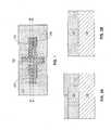
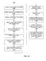
- FIG. 1is a top sectional view of one exemplary embodiment of an apparatus incorporating GAA nanowire architecture in which a gate is positioned transverse to a nanowire;
- FIG. 2Ais a side view along cross section A-A′ of FIG. 1 during a step in the fabrication of the apparatus;
- FIG. 2Bis a side view along cross section B-B′ of FIG. 1 during a step in the fabrication of the apparatus;
- FIG. 3Ais a side view along cross section A-A′ during a step of forming a dummy gate stack over a nanowire in the fabrication of the apparatus;
- FIG. 3Bis a side view along cross section B-B′ during the step of forming the dummy gate stack in the fabrication of the apparatus;
- FIG. 4Ais a side view along cross section A-A′ during a step of etching an insulator layer in the fabrication of the apparatus;
- FIG. 4Bis a side view along cross section B-B′ during the step of etching the insulator layer in the fabrication of the apparatus;
- FIG. 5Ais a side view along cross section A-A′ during a step of forming a spacer on the dummy gate stack in the fabrication of the apparatus;
- FIG. 5Bis a side view along cross section B-B′ during the step of forming the spacer on the dummy gate stack in the fabrication of the apparatus;
- FIG. 6Ais a side view along cross section A-A′ during a step of forming source/drain regions in the fabrication of the apparatus;
- FIG. 6Bis a side view along cross section B-B′ during the step of forming source/drain regions in the fabrication of the apparatus;
- FIG. 7Ais a side view along cross section A-A′ during a step of depositing an interlayer dielectric and applying a chemical mechanical polish in the fabrication of the apparatus;
- FIG. 7Bis a side view along cross section B-B′ during the step of depositing the interlayer dielectric and applying the chemical mechanical polish in the fabrication of the apparatus;
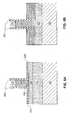
- FIG. 8Ais a side view along cross section A-A′ during a step of removing the dummy gate in the fabrication of the apparatus;
- FIG. 8Bis a side view along cross section B-B′ during the step of removing the dummy gate in the fabrication of the apparatus;
- FIG. 9Ais a side view along cross section A-A′ during a step of undercutting the nanowire in the fabrication of the apparatus;
- FIG. 9Bis a side view along cross section B-B′ during the step of removing portions of the insulator layer in the fabrication of the apparatus;
- FIG. 10Ais a side view along cross section A-A′ during a step of forming a replacement gate in the fabrication of the apparatus;
- FIG. 10Bis a side view along cross section B-B′ during the step of forming the replacement gate in the fabrication of the apparatus;
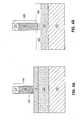
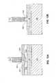
- FIG. 11Ais a cross sectional side view of a prior art apparatus taken along a nanowire in which during undercutting of an insulating layer, the insulating layer was laterally etched underneath spacers of the apparatus;
- FIG. 11Bis a cross sectional side view of the prior art apparatus of FIG. 11A in which during undercutting of the insulating layer, the insulating layer was laterally etched underneath spacers of the apparatus;
- FIG. 12Ais a side view along cross section A-A′ during a step of forming a second exemplary embodiment of an apparatus in which the source/drain regions undercut the gate stack and the nanowire;
- FIG. 12Bis a side view along cross section B-B′ during the step of forming the second exemplary embodiment of the apparatus in which the source/drain regions undercut the gate stack;
- FIG. 13Ais a side view along cross section A-A′ during a step of extending the spacers under the nanowire;
- FIG. 13Bis a side view along cross section B-B′ during the step of extending the spacers under the gate stack.
- FIG. 14is a flow of a method of forming a GAA nanowire structure.
- GAA nanowire architectureis used in the fabrication of a CMOS such as a MOSFET to allow for improved electrostatic gate control in a conducting channel and to offer the potential to drive more current per device area than is possible in conventional planar CMOS architectures.
- a dummy gatecomprising an oxide material is formed over a nanowire so as to extend substantially transverse to the nanowire. Lower portions of the dummy gate extend below and underneath the nanowire and into a surface on which the nanowire is disposed. Upper portions of the material of the dummy gate are removed, and lower portions of the material of the dummy gate (the oxide under the nanowire extending between source and drain regions) are recessed and undercut. Spacers are then formed on opposing sides of the dummy gate. When the oxide is undercut after removal of the upper portions of the dummy gate, the lateral extent of the opening is limited by the presence of the spacers.
- a GAA nanowire structure for a MOSFETis designated generally by the reference number 100 and is hereinafter referred to as “apparatus 100 .”
- Apparatus 100comprises a nanowire 110 generally laterally disposed on an insulator layer 120 , the insulator layer 120 being disposed on a substrate (shown at 130 in FIGS. 2A-10B ).
- Cross section A-A′is parallel to and coincident with the nanowire 110
- cross section B-B′is parallel to the nanowire 110 and between the nanowire 110 and a second nanowire (not shown) positioned parallel to and distal from the nanowire 110 .
- the insulator layer 120may be a buried oxide (BOX) layer.
- the nanowire 110may be epitaxially grown on the insulator layer 120 using chemical vapor deposition (CVD) or any other suitable method. Source regions 220 and drain regions 230 are deposited on and adjacent to the nanowire 110 by epitaxy.
- CVDchemical vapor deposition
- one or more patternsare laid out for the epitaxial growth (or other formation) of nanowires 110 as channels on the insulator layer 120 of a silicon-on-insulator (SOI) wafer.
- the nanowire 110is patterned onto the insulator layer 120 by any suitable method.
- Methods by which the nanowire may be patterned onto the insulator layer 120include, but are not limited to, lithographic techniques such as atomic force microscope (AFM) nano-oxidation and selective wet etching, E-beam lithography, and X-ray lithography.
- AFMatomic force microscope
- the SOI waferis defined by the substrate 130 and the insulator layer 120 .
- the substrate 130may comprise any semiconducting material such as, for example, silicon carbide (SiC), silicon alloys, germanium, germanium alloys, alloys of silicon and germanium (Si x Ge y ), gallium arsenide (GaAs), indium arsenide (InAs), indium phosphide (InP), and the like.
- the insulator layer 120may comprise, for example, silicon dioxide (SiO 2 ) or the like.
- the one or more nanowires 110are then epitaxially grown to form the channels.
- the nanowire 110may comprise silicon, germanium, boron-doped germanium, or any other suitable material.
- a nanowireis not patterned onto the insulator layer 120 on a portion of the insulator layer 120 along the cross section B-B′ parallel to the nanowire 110 and between the nanowire 110 and a second nanowire.
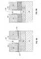
- a dummy gate stack 140is formed both on the nanowire 110 ( FIG. 3A ) and on the insulator layer 120 ( FIG. 3B ).
- the dummy gate stack 140may be substantially transverse to the nanowire 110 .
- a dielectric layer 150is deposited or grown, on a surface of the nanowire 110 .
- This dielectric layer 150comprises, for example, SiO 2 , alumina (Al 2 O 3 ), tantalum pentoxide (Ta 2 O 5 ), hafnium dioxide (HfO 2 ), or the like, deposited onto the nanowire 110 by, for example, thermal oxidation, atmospheric pressure CVD (APCVD), low pressure CVD (LPCVD), sputtering techniques, or electron-beam deposition.
- APCVDatmospheric pressure CVD
- LPCVDlow pressure CVD
- sputtering techniquesor electron-beam deposition.
- a dummy gate electrode 160is deposited onto the dielectric layer 150 and onto the insulator layer 120 .
- the dummy gate electrode 160may comprise, for example, polysilicon (or metal or a combination of polysilicon and metal) and may be deposited via LPCVD or any other suitable method.
- a dummy gate cap 170is deposited onto the dummy gate electrode 160 .
- the dummy gate cap 170may comprise, for example, a nitride (silicon nitride, carbon nitride, or the like) or a silicide and may be deposited via LPCVD.
- the material of the insulator layer 120(e.g., the SiO 2 ) is etched vertically.
- the dummy gate stack 140 and the nanowire 110are used as a mask to prevent the etching of the insulator layer 120 underneath the dummy gate stack 140 and the nanowire 110 .
- the material of the insulator layer 120is removed by the etch to form recesses 180 .
- Etching of the insulator layer 120 to form the recesses 180may be effected by wet etch techniques (e.g., polyphosphoric acids, hydrofluoric acid (HF), potassium hydroxide, or the like) or plasma or gas etch techniques. Irrespective of the technique used to etch, the material of the insulator layer 120 is recessed vertically from the outer surfaces of the dummy gate stack 140 such that the insulator layer 120 directly under the dummy gate 120 is not removed.
- wet etch techniquese.g., polyphosphoric acids, hydrofluoric acid (HF), potassium hydroxide
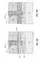
- spacers 200are formed on opposing sides of the dummy gate stack 140 , as shown in FIGS. 5A and 5B .
- the spacers 200extend from the top of the dummy gate cap 170 to the nanowire 110 .
- the spacers 200extend to a depth below the bottom of the nanowire 110 and the dummy gate stack. 140 (to the bottom surfaces defined by the recesses 180 ).
- the spacers 200are formed by masking off the nanowire 110 and the insulator layer 120 and depositing dielectric material, such as SiO 2 , silicon nitride, low-permittivity (low-K) dielectrics such as SiO x N y or boron nitride, via CVD or LPCVD.
- dielectric materialsuch as SiO 2 , silicon nitride, low-permittivity (low-K) dielectrics such as SiO x N y or boron nitride, via CVD or LPCVD.
- a source and a drainmay be formed by a selective epitaxial growth process such as vapor phase epitaxy, which is a form of CVD.
- Epitaxial growthrefers to the deposition of a crystalline overlayer on a crystalline sub-layer where the structure of the overlayer registers with the structure of the crystalline sub-layer.
- a layer of source material and drain materialis epitaxially grown on opposing sides of the dummy gate stack 140 and over the nanowire 110 to form the source regions 220 and drain regions 230 .
- FIG. 6Aa layer of source material and drain material is epitaxially grown on opposing sides of the dummy gate stack 140 and over the nanowire 110 to form the source regions 220 and drain regions 230 .
- a layer of the material used to grow the source regions 220 and the drain regions 230is also epitaxially grown on the insulator layer 120 at opposing sides of the dummy gate stack 140 and over the cross section B-B′ parallel to the nanowire 110 and between the nanowire 110 and a second nanowire.
- an interlayer dielectric (ILD) 250is deposited onto the epitaxially grown source regions 220 and drain regions 230 by CVD.
- the resulting structureis then planarized using a chemical mechanical polish (CMP).
- Materials from which the ILD 250 may be formedinclude oxides such as SiO 2 .
- the dummy gate cap 170 and the dummy gate electrode 160are removed in an etching process that comprises one or more of a dry etch process (e.g., a reactive ion etch (RIE), plasma etching, or the like) and a wet etch process using phosphoric acid (H 3 PO 4 ).
- a dry etch processe.g., a reactive ion etch (RIE), plasma etching, or the like
- H 3 PO 4phosphoric acid
- the dummy gate cap 170is removed using the dry etch process.
- the dummy gate electrode 160is removed using the RIE. Top portions of the spacers 200 are removed down to the bottom surface of the dummy gate cap 170 , but bottom portions of the spacers 200 remain in the ILD 250 .
- Etching in the vertical directionis then carried out along with an isotropic etch (such as aqueous HF, dilute aqueous HF, HF vapor, buffered oxide etch (e.g., NH 4 F:HF), or the like) to remove the dielectric layer 150 (the oxide) and portions of the insulator layer 120 down to a depth at or below a bottom surface of the nanowire 110 and between the spacers.
- an isotropic etchsuch as aqueous HF, dilute aqueous HF, HF vapor, buffered oxide etch (e.g., NH 4 F:HF), or the like
- the dry etch process and/or the wet etch process along with the isotropic etchforms a trench 260 that extends in the insulator layer 120 transverse to cross section A-A′ and cross section B-B′ and leaves portions of the nanowire(s) 110 extending between the spacer 200 exposed.
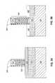
- FIG. 9Afurther isotropic etching results in additional insulator layer 120 being removed and the nanowire 110 being undercut such that the bottom portion of the nanowire 110 is released from the source regions 220 and the drain regions 230 .
- the nanowire 110is essentially suspended between the source region 220 and the drain region 230 .
- the sides of the opening formed under the nanowire 110 by the isotropic etchare substantially coplanar with the inner facing surfaces of the spacers 200 , which are formed before the nanowire is suspended between the source regions 220 and the drain regions 230 .
- FIG. 9Blateral undercutting of the insulator layer 120 is prevented or at least limited by the spacers 200 .
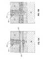
- a replacement gate 300is formed in the space between the spacers 200 .
- a layer 310 of high-k dielectric materialis deposited on the surfaces defining the opening between the spacers 200 as well as on nanowire 110 ( FIG. 10A ).
- This layer 310 of high-k dielectric materialmay be deposited by, for example, CVD.
- the high-k dielectric materialmay be, for example, oxide(s) of tantalum, zirconium, or aluminum, as well as SiO 2 or Al 3 N 4 .
- a gate metalis deposited on the layer 310 of high-k dielectric material.
- the gate metalis preferably aluminum, nickel, tantalum, tantalum nitride, titanium, titanium nitride, TiAl alloy, ruthenium, tungsten, or the like and is deposited on the high-k dielectric material via vapor deposition.
- Formation of the replacement gate 300 as indicatedis different than the formation of similar gates in the known art, as shown in FIGS. 11A and 11B , in which portions of a gate 330 and/or a layer 340 of dielectric material extend laterally underneath spacers 200 by a distance d. In the formation of the replacement gate 300 as in FIGS.
- the oxide layeris laterally etched during the undercutting process.
- the portion of the replacement gate 300 under the nanowire 110 and between the nanowiresis narrower.
- the material of the source regions 220 and the drain regions 230is subjected to a vertical etching process along with an isotropic etching process (oxide undercutting) carried out in lateral directions to form recesses (shown at 400 ) underneath the dummy gate stack 140 as well as recesses (shown at 410 ) underneath the nanowire 110 in outward directions toward the source region 220 and the drain regions 230 .
- an isotropic etching processoxygen undercutting
- lower portions of the spacers 200 along cross section A-A′are extended under the nanowire 110 ( FIG. 13A ) both inwardly of the gate region to fill the recesses 400 as well as in the outward directions underneath the nanowire 110 toward the source region 220 and the drain region 230 .
- Lower portions of the spacers 200 between nanowiresare laterally extended into the recesses 400 .
- the layer 310 of high-k dielectric materialis deposited, and the replacement gate 300 is formed on the layer 310 of high-k dielectric material.
- portions of the replacement gate 300 under the nanowire 110 both directly under the nanowire 110 and in the spaces between nanowiresare narrower as compared to gates in the known art.
- Method 1400comprises a providing step 1405 in which an insulator layer is generally provided on a substrate. After the providing step 1405 , a nanowire is patterned onto the insulator layer in a patterning step 1410 . A dielectric layer is then deposited onto the nanowire in a dielectric layer deposit step 1415 . A dummy gate electrode is then deposited onto the dielectric layer in a dummy gate electrode deposit step 1420 . A dummy gate cap is then deposited onto the dummy gate electrode in a dummy gate cap deposit step 1425 .
- the insulator layeris then etched in an insulator layer etch step 1430 , and spacers are formed on opposing sides of the dummy stack in a spacer formation step 1435 .
- Source and drain regionsare then formed on opposing sides of the dummy stack in a source/drain region formation step 1440 .
- An ILD layeris deposited onto the source/drain regions in an ILD deposit step 1445 , and the ILD is planarized in a planarize step 1450 .
- the dummy gate cap and dummy gate electrodeare then removed in a removal step 1455 , and the nanowire is undercut in an undercutting step 1460 to cause the nanowire to be suspended between the source/drain regions.
- a replacement gateis formed in a replacement gate formation step 1465 .
Landscapes
- Chemical & Material Sciences (AREA)
- Engineering & Computer Science (AREA)
- Materials Engineering (AREA)
- Nanotechnology (AREA)
- Thin Film Transistor (AREA)
- Composite Materials (AREA)
Abstract
Description
- This application is a continuation of U.S. patent application Ser. No. 14/532,122, filed on Nov. 4, 2014, which is a continuation of U.S. patent application Ser. No. 14/046,069, filed on Oct. 4, 2013, which is a continuation of U.S. patent application Ser. No. 14/035,060, filed on Sep. 24, 2013, the contents of all of the foregoing applications being incorporated herein by reference in their entireties.
- The exemplary embodiments of this invention relate generally to semiconductor devices and, more particularly, to a complementary metal oxide semiconductor device having a gate-all-around nanowire structure.
- A complementary metal oxide semiconductor device (CMOS) uses symmetrically-oriented pairs of p-type and n-type metal oxide semiconductor field effect transistors (MOSFETs) arranged on silicon or silicon-on-insulator (SOI) substrates. Source and drain regions associated with each MOSFET are connected by a channel. A gate disposed adjacent the channel controls the flow of current between the source and drain regions. The channel may be defined by a thin “fin” or other structure that provides surface(s) through which the gate controls the flow of current.
- In a device such as a gate-all-around (GAA) nanowire MOSFET, the channel between the source and drain regions is a nanowire, and the gate surrounds the nanowire. Formation of such a gate so as to wrap around the nanowire is a challenge. For example, it is often difficult (if not impossible) to pattern the portion of the gate that is located underneath the nanowire. Hence, the bottom portion of the gate may become longer than the top portion and may overlap the source and drain regions of the device.
- In fabricating a GAA nanowire MOSFET, a dummy gate is generally formed as a sacrificial structure to facilitate patterning to achieve a desired alignment and/or the implantation of ions for doping purposes. A replacement gate flow is then used to remove the dummy gate and install a permanent replacement gate. In the replacement gate flow, the dummy gate is patterned. The nanowire is then released from the dummy gate by the removal of the dummy gate. In removing the dummy gate, the material underneath the nanowire is undercut to cause the complete release of the wire from the material of the dummy gate and to form an opening that can be filled with a GAA structure. However, the undercutting also extends the opening in the directions toward the source and drain, thereby adding to the parasitic capacitance of the MOSFET.
- In one exemplary aspect, a method for fabricating a semiconductor device comprises forming a nanowire on an insulator layer at a surface of a substrate; forming a dummy gate over a portion of the nanowire and a portion of the insulator layer; forming recesses in the insulator layer on opposing sides of the dummy gate; forming spacers on opposing sides of the dummy gate; forming source regions and drain regions in the recesses in the insulator layer on opposing sides of the dummy gate; depositing an interlayer dielectric on the source regions and the drain regions; removing the dummy gate to form a trench; removing the insulator layer under the nanowire such that a width of the trench underneath the nanowire is equal to or less than a distance between the spacers; and forming a replacement gate in the trench.
- In another exemplary aspect, a method for fabricating a semiconductor device comprises forming a dummy gate stack over a portion of and substantially transverse to a nanowire on a silicon-on-insulator wafer; forming recesses in the silicon-on-insulator wafer on opposing sides of the dummy gate stack; forming spacers in the recesses on opposing sides of the dummy gate stack; forming source regions and drain regions on opposing sides of the spacers; depositing an interlayer dielectric on the source regions and the drain regions; planarizing an upper surface defined by the interlayer dielectric, upper edges of the spacers, and an upper surface of the dummy gate stack; removing the dummy gate stack; removing a portion of the silicon-on-insulator wafer underneath the dummy gate stack, underneath the nanowire, and between inner facing surfaces of the spacers; and forming a replacement gate in place of the dummy gate stack, the replacement gate extending at least under the nanowire to form a gate-all-around structure and extending between the inner facing surfaces of the spacers.
- In another exemplary aspect, an apparatus for a semiconductor device comprises a nanowire formed on an insulator layer disposed on a substrate of semiconductor material, a first end of the nanowire being in communication with a source region and a second end of the nanowire being in communication with a drain region; and a gate positioned across and extending substantially transverse to the nanowire between the source region and the drain region, the gate comprising an electrode and spacers positioned on opposing sides of the electrode and extending substantially transverse to the nanowire. A bottom portion of the gate surrounds a portion of the nanowire extending from the source region to the drain region, and outer surfaces of the gate extend vertically downward into the insulator layer but do not extend beyond the inner faces of the spacers toward the source region and the drain region.
- The foregoing and other aspects of the exemplary embodiments are made more evident in the following Detailed Description, when read in conjunction with the attached Drawing Figures, wherein:
FIG. 1 is a top sectional view of one exemplary embodiment of an apparatus incorporating GAA nanowire architecture in which a gate is positioned transverse to a nanowire;FIG. 2A is a side view along cross section A-A′ ofFIG. 1 during a step in the fabrication of the apparatus;FIG. 2B is a side view along cross section B-B′ ofFIG. 1 during a step in the fabrication of the apparatus;FIG. 3A is a side view along cross section A-A′ during a step of forming a dummy gate stack over a nanowire in the fabrication of the apparatus;FIG. 3B is a side view along cross section B-B′ during the step of forming the dummy gate stack in the fabrication of the apparatus;FIG. 4A is a side view along cross section A-A′ during a step of etching an insulator layer in the fabrication of the apparatus;FIG. 4B is a side view along cross section B-B′ during the step of etching the insulator layer in the fabrication of the apparatus;FIG. 5A is a side view along cross section A-A′ during a step of forming a spacer on the dummy gate stack in the fabrication of the apparatus;FIG. 5B is a side view along cross section B-B′ during the step of forming the spacer on the dummy gate stack in the fabrication of the apparatus;FIG. 6A is a side view along cross section A-A′ during a step of forming source/drain regions in the fabrication of the apparatus;FIG. 6B is a side view along cross section B-B′ during the step of forming source/drain regions in the fabrication of the apparatus;FIG. 7A is a side view along cross section A-A′ during a step of depositing an interlayer dielectric and applying a chemical mechanical polish in the fabrication of the apparatus;FIG. 7B is a side view along cross section B-B′ during the step of depositing the interlayer dielectric and applying the chemical mechanical polish in the fabrication of the apparatus;FIG. 8A is a side view along cross section A-A′ during a step of removing the dummy gate in the fabrication of the apparatus;FIG. 8B is a side view along cross section B-B′ during the step of removing the dummy gate in the fabrication of the apparatus;FIG. 9A is a side view along cross section A-A′ during a step of undercutting the nanowire in the fabrication of the apparatus;FIG. 9B is a side view along cross section B-B′ during the step of removing portions of the insulator layer in the fabrication of the apparatus;FIG. 10A is a side view along cross section A-A′ during a step of forming a replacement gate in the fabrication of the apparatus;FIG. 10B is a side view along cross section B-B′ during the step of forming the replacement gate in the fabrication of the apparatus;FIG. 11A is a cross sectional side view of a prior art apparatus taken along a nanowire in which during undercutting of an insulating layer, the insulating layer was laterally etched underneath spacers of the apparatus;FIG. 11B is a cross sectional side view of the prior art apparatus ofFIG. 11A in which during undercutting of the insulating layer, the insulating layer was laterally etched underneath spacers of the apparatus;FIG. 12A is a side view along cross section A-A′ during a step of forming a second exemplary embodiment of an apparatus in which the source/drain regions undercut the gate stack and the nanowire;FIG. 12B is a side view along cross section B-B′ during the step of forming the second exemplary embodiment of the apparatus in which the source/drain regions undercut the gate stack;FIG. 13A is a side view along cross section A-A′ during a step of extending the spacers under the nanowire;FIG. 13B is a side view along cross section B-B′ during the step of extending the spacers under the gate stack; andFIG. 14 is a flow of a method of forming a GAA nanowire structure.- In the exemplary embodiments disclosed herein, GAA nanowire architecture is used in the fabrication of a CMOS such as a MOSFET to allow for improved electrostatic gate control in a conducting channel and to offer the potential to drive more current per device area than is possible in conventional planar CMOS architectures. In implementing the GAA nanowire architecture, a dummy gate comprising an oxide material is formed over a nanowire so as to extend substantially transverse to the nanowire. Lower portions of the dummy gate extend below and underneath the nanowire and into a surface on which the nanowire is disposed. Upper portions of the material of the dummy gate are removed, and lower portions of the material of the dummy gate (the oxide under the nanowire extending between source and drain regions) are recessed and undercut. Spacers are then formed on opposing sides of the dummy gate. When the oxide is undercut after removal of the upper portions of the dummy gate, the lateral extent of the opening is limited by the presence of the spacers.
- Referring to
FIG. 1 , a GAA nanowire structure for a MOSFET is designated generally by thereference number 100 and is hereinafter referred to as “apparatus 100.”Apparatus 100 comprises ananowire 110 generally laterally disposed on aninsulator layer 120, theinsulator layer 120 being disposed on a substrate (shown at130 inFIGS. 2A-10B ). Cross section A-A′ is parallel to and coincident with thenanowire 110, and cross section B-B′ is parallel to thenanowire 110 and between thenanowire 110 and a second nanowire (not shown) positioned parallel to and distal from thenanowire 110. In thefinished apparatus 100, theinsulator layer 120 may be a buried oxide (BOX) layer. In an exemplary embodiment, thenanowire 110 may be epitaxially grown on theinsulator layer 120 using chemical vapor deposition (CVD) or any other suitable method.Source regions 220 anddrain regions 230 are deposited on and adjacent to thenanowire 110 by epitaxy. - Referring now to
FIG. 2A , one or more patterns are laid out for the epitaxial growth (or other formation) ofnanowires 110 as channels on theinsulator layer 120 of a silicon-on-insulator (SOI) wafer. Thenanowire 110 is patterned onto theinsulator layer 120 by any suitable method. Methods by which the nanowire may be patterned onto theinsulator layer 120 include, but are not limited to, lithographic techniques such as atomic force microscope (AFM) nano-oxidation and selective wet etching, E-beam lithography, and X-ray lithography. - The SOI wafer is defined by the
substrate 130 and theinsulator layer 120. Thesubstrate 130 may comprise any semiconducting material such as, for example, silicon carbide (SiC), silicon alloys, germanium, germanium alloys, alloys of silicon and germanium (SixGey), gallium arsenide (GaAs), indium arsenide (InAs), indium phosphide (InP), and the like. Theinsulator layer 120 may comprise, for example, silicon dioxide (SiO2) or the like. - The one or
more nanowires 110 are then epitaxially grown to form the channels. Thenanowire 110 may comprise silicon, germanium, boron-doped germanium, or any other suitable material. - As shown in
FIG. 2B , a nanowire is not patterned onto theinsulator layer 120 on a portion of theinsulator layer 120 along the cross section B-B′ parallel to thenanowire 110 and between thenanowire 110 and a second nanowire. - Referring now to
FIGS. 3A and 3B , adummy gate stack 140 is formed both on the nanowire110 (FIG. 3A ) and on the insulator layer120 (FIG. 3B ). Thedummy gate stack 140 may be substantially transverse to thenanowire 110. In forming thedummy gate stack 140 across thenanowire 110, adielectric layer 150 is deposited or grown, on a surface of thenanowire 110. Thisdielectric layer 150 comprises, for example, SiO2, alumina (Al2O3), tantalum pentoxide (Ta2O5), hafnium dioxide (HfO2), or the like, deposited onto thenanowire 110 by, for example, thermal oxidation, atmospheric pressure CVD (APCVD), low pressure CVD (LPCVD), sputtering techniques, or electron-beam deposition. - Subsequent to the deposition or growth of the
dielectric layer 150, adummy gate electrode 160 is deposited onto thedielectric layer 150 and onto theinsulator layer 120. Thedummy gate electrode 160 may comprise, for example, polysilicon (or metal or a combination of polysilicon and metal) and may be deposited via LPCVD or any other suitable method. - Subsequent to the deposition of the
dummy gate electrode 160, adummy gate cap 170 is deposited onto thedummy gate electrode 160. Thedummy gate cap 170 may comprise, for example, a nitride (silicon nitride, carbon nitride, or the like) or a silicide and may be deposited via LPCVD. - Referring now to
FIGS. 4A and 4B , the material of the insulator layer120 (e.g., the SiO2) is etched vertically. As shown inFIG. 4A , thedummy gate stack 140 and thenanowire 110 are used as a mask to prevent the etching of theinsulator layer 120 underneath thedummy gate stack 140 and thenanowire 110. As shown inFIG. 4B , the material of theinsulator layer 120 is removed by the etch to form recesses180. Etching of theinsulator layer 120 to form therecesses 180 may be effected by wet etch techniques (e.g., polyphosphoric acids, hydrofluoric acid (HF), potassium hydroxide, or the like) or plasma or gas etch techniques. Irrespective of the technique used to etch, the material of theinsulator layer 120 is recessed vertically from the outer surfaces of thedummy gate stack 140 such that theinsulator layer 120 directly under thedummy gate 120 is not removed. - Once the
recesses 180 are formed in theinsulator layer 120,spacers 200 are formed on opposing sides of thedummy gate stack 140, as shown inFIGS. 5A and 5B . Along the cross section A-A′, thespacers 200 extend from the top of thedummy gate cap 170 to thenanowire 110. Between thenanowire 110 and adjacent nanowires, however, thespacers 200 extend to a depth below the bottom of thenanowire 110 and the dummy gate stack.140 (to the bottom surfaces defined by the recesses180). Thespacers 200 are formed by masking off thenanowire 110 and theinsulator layer 120 and depositing dielectric material, such as SiO2, silicon nitride, low-permittivity (low-K) dielectrics such as SiOxNyor boron nitride, via CVD or LPCVD. - Referring now to
FIGS. 6A and 6B , a source and a drain may be formed by a selective epitaxial growth process such as vapor phase epitaxy, which is a form of CVD. Epitaxial growth refers to the deposition of a crystalline overlayer on a crystalline sub-layer where the structure of the overlayer registers with the structure of the crystalline sub-layer. As can be seen inFIG. 6A , a layer of source material and drain material is epitaxially grown on opposing sides of thedummy gate stack 140 and over thenanowire 110 to form thesource regions 220 anddrain regions 230. As can be seen inFIG. 6B , a layer of the material used to grow thesource regions 220 and thedrain regions 230 is also epitaxially grown on theinsulator layer 120 at opposing sides of thedummy gate stack 140 and over the cross section B-B′ parallel to thenanowire 110 and between thenanowire 110 and a second nanowire. - As shown in
FIGS. 7A and 73 , an interlayer dielectric (ILD)250 is deposited onto the epitaxially grownsource regions 220 anddrain regions 230 by CVD. The resulting structure is then planarized using a chemical mechanical polish (CMP). Materials from which theILD 250 may be formed include oxides such as SiO2. - Referring now to
FIGS. 8A and 8B , thedummy gate cap 170 and thedummy gate electrode 160 are removed in an etching process that comprises one or more of a dry etch process (e.g., a reactive ion etch (RIE), plasma etching, or the like) and a wet etch process using phosphoric acid (H3PO4). Preferably, thedummy gate cap 170 is removed using the dry etch process. Once thedummy gate cap 170 is removed, thedummy gate electrode 160 is removed using the RIE. Top portions of thespacers 200 are removed down to the bottom surface of thedummy gate cap 170, but bottom portions of thespacers 200 remain in theILD 250. Etching in the vertical direction is then carried out along with an isotropic etch (such as aqueous HF, dilute aqueous HF, HF vapor, buffered oxide etch (e.g., NH4F:HF), or the like) to remove the dielectric layer150 (the oxide) and portions of theinsulator layer 120 down to a depth at or below a bottom surface of thenanowire 110 and between the spacers. The dry etch process and/or the wet etch process along with the isotropic etch forms atrench 260 that extends in theinsulator layer 120 transverse to cross section A-A′ and cross section B-B′ and leaves portions of the nanowire(s)110 extending between thespacer 200 exposed. - As shown in
FIG. 9A , further isotropic etching results inadditional insulator layer 120 being removed and thenanowire 110 being undercut such that the bottom portion of thenanowire 110 is released from thesource regions 220 and thedrain regions 230. Thus, thenanowire 110 is essentially suspended between thesource region 220 and thedrain region 230. The sides of the opening formed under thenanowire 110 by the isotropic etch are substantially coplanar with the inner facing surfaces of thespacers 200, which are formed before the nanowire is suspended between thesource regions 220 and thedrain regions 230. As shown inFIG. 9B , lateral undercutting of theinsulator layer 120 is prevented or at least limited by thespacers 200. - Referring now to
FIGS. 10A and 10B , areplacement gate 300 is formed in the space between thespacers 200. In a first step in forming the replacement gate300 (which may be a replacement metal gate (RMG)), alayer 310 of high-k dielectric material is deposited on the surfaces defining the opening between thespacers 200 as well as on nanowire110 (FIG. 10A ). Thislayer 310 of high-k dielectric material may be deposited by, for example, CVD. The high-k dielectric material may be, for example, oxide(s) of tantalum, zirconium, or aluminum, as well as SiO2or Al3N4. - In a second step of forming the
replacement gate 300, a gate metal is deposited on thelayer 310 of high-k dielectric material. The gate metal is preferably aluminum, nickel, tantalum, tantalum nitride, titanium, titanium nitride, TiAl alloy, ruthenium, tungsten, or the like and is deposited on the high-k dielectric material via vapor deposition. Formation of thereplacement gate 300 as indicated is different than the formation of similar gates in the known art, as shown inFIGS. 11A and 11B , in which portions of a gate330 and/or alayer 340 of dielectric material extend laterally underneathspacers 200 by a distance d. In the formation of thereplacement gate 300 as inFIGS. 10A and 10B (and similar gates) to form the GAA structure, the oxide layer is laterally etched during the undercutting process. Compared to the gate330 as shown inFIGS. 11A and 11B , the portion of thereplacement gate 300 under thenanowire 110 and between the nanowires is narrower. - In another exemplary embodiment, as shown in
FIGS. 12A and 12B , the material of thesource regions 220 and thedrain regions 230 is subjected to a vertical etching process along with an isotropic etching process (oxide undercutting) carried out in lateral directions to form recesses (shown at400) underneath thedummy gate stack 140 as well as recesses (shown at410) underneath thenanowire 110 in outward directions toward thesource region 220 and thedrain regions 230. Depending upon the extent of the undercutting ofdummy gate stack 140, portions of the nanowire110 (FIG. 12A ) may or may not be completely released. - Referring now to
FIGS. 13A and 13B , lower portions of thespacers 200 along cross section A-A′ are extended under the nanowire110 (FIG. 13A ) both inwardly of the gate region to fill therecesses 400 as well as in the outward directions underneath thenanowire 110 toward thesource region 220 and thedrain region 230. Lower portions of thespacers 200 between nanowires (e.g., along cross section B-B′) are laterally extended into therecesses 400. Thelayer 310 of high-k dielectric material is deposited, and thereplacement gate 300 is formed on thelayer 310 of high-k dielectric material. In such an embodiment, portions of thereplacement gate 300 under thenanowire 110 both directly under thenanowire 110 and in the spaces between nanowires are narrower as compared to gates in the known art. - Referring now to
FIG. 14 , one exemplary a method of forming a GAA nanowire structure is designated generally by thereference number 1400 and is hereinafter referred to as “method 1400.”Method 1400 comprises a providingstep 1405 in which an insulator layer is generally provided on a substrate. After the providingstep 1405, a nanowire is patterned onto the insulator layer in apatterning step 1410. A dielectric layer is then deposited onto the nanowire in a dielectriclayer deposit step 1415. A dummy gate electrode is then deposited onto the dielectric layer in a dummy gateelectrode deposit step 1420. A dummy gate cap is then deposited onto the dummy gate electrode in a dummy gatecap deposit step 1425. The insulator layer is then etched in an insulatorlayer etch step 1430, and spacers are formed on opposing sides of the dummy stack in aspacer formation step 1435. Source and drain regions are then formed on opposing sides of the dummy stack in a source/drainregion formation step 1440. An ILD layer is deposited onto the source/drain regions in anILD deposit step 1445, and the ILD is planarized in aplanarize step 1450. The dummy gate cap and dummy gate electrode are then removed in aremoval step 1455, and the nanowire is undercut in an undercutting step1460 to cause the nanowire to be suspended between the source/drain regions. Following the undercutting step1460, a replacement gate is formed in a replacementgate formation step 1465. - The terminology used herein is for the purpose of describing particular embodiments only and is not intended to be limiting of the invention. As used herein, the singular forms “a,” “an,” and “the” are intended to include the plural forms as well, unless the context clearly indicates otherwise. It will be further understood that the terms “comprises” and/or “comprising,” when used in this specification, specify the presence of stated features, integers, steps, operations, elements, and/or components, but do not preclude the presence or addition of one or more other features, integers, steps, operations, elements, components, and/or groups thereof.
- The description of the present invention has been presented for purposes of illustration and description, but is not intended to be exhaustive or limited to the invention in the form disclosed. Many modifications and variations will be apparent to those of ordinary skill in the art without departing from the scope and spirit of the invention. The embodiments were chosen and described in order to best explain the principles of the invention and the practical applications, and to enable others of ordinary skill in the art to understand the invention for various embodiments with various modifications as are suited to the particular uses contemplated.
Claims (19)
Priority Applications (1)
| Application Number | Priority Date | Filing Date | Title |
|---|---|---|---|
| US14/751,761US9324797B2 (en) | 2013-09-24 | 2015-06-26 | Gate-all-around nanowire MOSFET and method of formation |
Applications Claiming Priority (4)
| Application Number | Priority Date | Filing Date | Title |
|---|---|---|---|
| US14/035,060US8900951B1 (en) | 2013-09-24 | 2013-09-24 | Gate-all-around nanowire MOSFET and method of formation |
| US14/046,069US8969934B1 (en) | 2013-09-24 | 2013-10-04 | Gate-all-around nanowire MOSFET and method of formation |
| US14/532,122US9443948B2 (en) | 2013-09-24 | 2014-11-04 | Gate-all-around nanowire MOSFET and method of formation |
| US14/751,761US9324797B2 (en) | 2013-09-24 | 2015-06-26 | Gate-all-around nanowire MOSFET and method of formation |
Related Parent Applications (1)
| Application Number | Title | Priority Date | Filing Date |
|---|---|---|---|
| US14/532,122ContinuationUS9443948B2 (en) | 2013-09-24 | 2014-11-04 | Gate-all-around nanowire MOSFET and method of formation |
Publications (2)
| Publication Number | Publication Date |
|---|---|
| US20150295039A1true US20150295039A1 (en) | 2015-10-15 |
| US9324797B2 US9324797B2 (en) | 2016-04-26 |
Family
ID=51948319
Family Applications (8)
| Application Number | Title | Priority Date | Filing Date |
|---|---|---|---|
| US14/035,060ActiveUS8900951B1 (en) | 2013-09-24 | 2013-09-24 | Gate-all-around nanowire MOSFET and method of formation |
| US14/046,069ActiveUS8969934B1 (en) | 2013-09-24 | 2013-10-04 | Gate-all-around nanowire MOSFET and method of formation |
| US14/532,122Active2033-12-14US9443948B2 (en) | 2013-09-24 | 2014-11-04 | Gate-all-around nanowire MOSFET and method of formation |
| US14/751,493ActiveUS9324795B2 (en) | 2013-09-24 | 2015-06-26 | Gate-all-around nanowire MOSFET and method of formation |
| US14/751,706ActiveUS9299777B2 (en) | 2013-09-24 | 2015-06-26 | Gate-all-around nanowire MOSFET and method of formation |
| US14/751,761ActiveUS9324797B2 (en) | 2013-09-24 | 2015-06-26 | Gate-all-around nanowire MOSFET and method of formation |
| US14/751,542ActiveUS9293532B2 (en) | 2013-09-24 | 2015-06-26 | Gate-all-around nanowire MOSFET and method of formation |
| US14/751,646ActiveUS9324796B2 (en) | 2013-09-24 | 2015-06-26 | Gate-all-around nanowire MOSFET and method of formation |
Family Applications Before (5)
| Application Number | Title | Priority Date | Filing Date |
|---|---|---|---|
| US14/035,060ActiveUS8900951B1 (en) | 2013-09-24 | 2013-09-24 | Gate-all-around nanowire MOSFET and method of formation |
| US14/046,069ActiveUS8969934B1 (en) | 2013-09-24 | 2013-10-04 | Gate-all-around nanowire MOSFET and method of formation |
| US14/532,122Active2033-12-14US9443948B2 (en) | 2013-09-24 | 2014-11-04 | Gate-all-around nanowire MOSFET and method of formation |
| US14/751,493ActiveUS9324795B2 (en) | 2013-09-24 | 2015-06-26 | Gate-all-around nanowire MOSFET and method of formation |
| US14/751,706ActiveUS9299777B2 (en) | 2013-09-24 | 2015-06-26 | Gate-all-around nanowire MOSFET and method of formation |
Family Applications After (2)
| Application Number | Title | Priority Date | Filing Date |
|---|---|---|---|
| US14/751,542ActiveUS9293532B2 (en) | 2013-09-24 | 2015-06-26 | Gate-all-around nanowire MOSFET and method of formation |
| US14/751,646ActiveUS9324796B2 (en) | 2013-09-24 | 2015-06-26 | Gate-all-around nanowire MOSFET and method of formation |
Country Status (1)
| Country | Link |
|---|---|
| US (8) | US8900951B1 (en) |
Cited By (1)
| Publication number | Priority date | Publication date | Assignee | Title |
|---|---|---|---|---|
| TWI624871B (en)* | 2015-12-16 | 2018-05-21 | 格羅方德半導體公司 | The horizontal gate is isolated from the bottom of the nanowire transistor |
Families Citing this family (286)
| Publication number | Priority date | Publication date | Assignee | Title |
|---|---|---|---|---|
| US20130023129A1 (en) | 2011-07-20 | 2013-01-24 | Asm America, Inc. | Pressure transmitter for a semiconductor processing environment |
| US10714315B2 (en) | 2012-10-12 | 2020-07-14 | Asm Ip Holdings B.V. | Semiconductor reaction chamber showerhead |
| US20160376700A1 (en) | 2013-02-01 | 2016-12-29 | Asm Ip Holding B.V. | System for treatment of deposition reactor |
| KR102083494B1 (en)* | 2013-10-02 | 2020-03-02 | 삼성전자 주식회사 | Semiconductor device including nanowire transistor |
| US9048301B2 (en) | 2013-10-16 | 2015-06-02 | Taiwan Semiconductor Manufacturing Company Limited | Nanowire MOSFET with support structures for source and drain |
| EP2887399B1 (en)* | 2013-12-20 | 2017-08-30 | Imec | A method for manufacturing a transistor device and associated device |
| US9324842B2 (en)* | 2013-12-20 | 2016-04-26 | Globalfoundries Inc. | Buried local interconnect in finfet structure and method of fabricating same |
| US9508830B2 (en)* | 2014-01-23 | 2016-11-29 | Taiwan Semiconductor Manufacturing Company Limited | Method of forming FinFET |
| US9236397B2 (en)* | 2014-02-04 | 2016-01-12 | Globalfoundries Inc. | FinFET device containing a composite spacer structure |
| US9985026B2 (en)* | 2014-08-15 | 2018-05-29 | Taiwan Semiconductor Manufacturing Co., Ltd. | Transistor, integrated circuit and method of fabricating the same |
| US9893159B2 (en) | 2014-08-15 | 2018-02-13 | Taiwan Semiconductor Manufacturing Co., Ltd. | Transistor, integrated circuit and method of fabricating the same |
| US10941490B2 (en) | 2014-10-07 | 2021-03-09 | Asm Ip Holding B.V. | Multiple temperature range susceptor, assembly, reactor and system including the susceptor, and methods of using the same |
| US9502567B2 (en)* | 2015-02-13 | 2016-11-22 | Taiwan Semiconductor Manufacturing Co., Ltd. | Semiconductor fin structure with extending gate structure |
| US9929242B2 (en)* | 2015-01-12 | 2018-03-27 | Taiwan Semiconductor Manufacturing Co., Ltd. | Semiconductor device and manufacturing method thereof |
| US10276355B2 (en) | 2015-03-12 | 2019-04-30 | Asm Ip Holding B.V. | Multi-zone reactor, system including the reactor, and method of using the same |
| US9768261B2 (en) | 2015-04-17 | 2017-09-19 | Taiwan Semiconductor Manufacturing Company Ltd. | Semiconductor structure and method of forming the same |
| US10458018B2 (en) | 2015-06-26 | 2019-10-29 | Asm Ip Holding B.V. | Structures including metal carbide material, devices including the structures, and methods of forming same |
| US9741792B2 (en) | 2015-10-21 | 2017-08-22 | International Business Machines Corporation | Bulk nanosheet with dielectric isolation |
| US10211308B2 (en) | 2015-10-21 | 2019-02-19 | Asm Ip Holding B.V. | NbMC layers |
| US9419102B1 (en)* | 2015-12-11 | 2016-08-16 | International Business Machines Corporation | Method to reduce parasitic gate capacitance and structure for same |
| KR102409962B1 (en) | 2015-12-16 | 2022-06-16 | 삼성전자주식회사 | Semiconductor device |
| US11139308B2 (en) | 2015-12-29 | 2021-10-05 | Asm Ip Holding B.V. | Atomic layer deposition of III-V compounds to form V-NAND devices |
| US10529554B2 (en) | 2016-02-19 | 2020-01-07 | Asm Ip Holding B.V. | Method for forming silicon nitride film selectively on sidewalls or flat surfaces of trenches |
| US9472471B1 (en) | 2016-03-01 | 2016-10-18 | International Business Machines Corporation | Hybrid orientation vertically stacked III-V and Ge gate-all-around CMOS |
| KR102413610B1 (en) | 2016-03-02 | 2022-06-24 | 삼성전자주식회사 | Layout design system, Semiconductor device and method for fabricating the same using the design system |
| US10343920B2 (en) | 2016-03-18 | 2019-07-09 | Asm Ip Holding B.V. | Aligned carbon nanotubes |
| US9911660B2 (en)* | 2016-04-26 | 2018-03-06 | Lam Research Corporation | Methods for forming germanium and silicon germanium nanowire devices |
| US11453943B2 (en) | 2016-05-25 | 2022-09-27 | Asm Ip Holding B.V. | Method for forming carbon-containing silicon/metal oxide or nitride film by ALD using silicon precursor and hydrocarbon precursor |
| KR102422240B1 (en) | 2016-05-26 | 2022-07-18 | 삼성전자주식회사 | Integrated circuit device and method of manufacturing the same |
| KR20170135115A (en) | 2016-05-30 | 2017-12-08 | 삼성전자주식회사 | Semiconductor device and method for fabricating the same |
| US11004985B2 (en) | 2016-05-30 | 2021-05-11 | Samsung Electronics Co., Ltd. | Semiconductor device having multi-thickness nanowire |
| US10612137B2 (en) | 2016-07-08 | 2020-04-07 | Asm Ip Holdings B.V. | Organic reactants for atomic layer deposition |
| US9859151B1 (en) | 2016-07-08 | 2018-01-02 | Asm Ip Holding B.V. | Selective film deposition method to form air gaps |
| US9887082B1 (en) | 2016-07-28 | 2018-02-06 | Asm Ip Holding B.V. | Method and apparatus for filling a gap |
| US9812320B1 (en) | 2016-07-28 | 2017-11-07 | Asm Ip Holding B.V. | Method and apparatus for filling a gap |
| KR102460862B1 (en) | 2016-08-04 | 2022-10-28 | 삼성전자주식회사 | Semiconductor device |
| US9842927B1 (en)* | 2016-08-26 | 2017-12-12 | Globalfoundries Inc. | Integrated circuit structure without gate contact and method of forming same |
| US9679780B1 (en) | 2016-09-28 | 2017-06-13 | International Business Machines Corporation | Polysilicon residue removal in nanosheet MOSFETs |
| US11532757B2 (en) | 2016-10-27 | 2022-12-20 | Asm Ip Holding B.V. | Deposition of charge trapping layers |
| US10714350B2 (en) | 2016-11-01 | 2020-07-14 | ASM IP Holdings, B.V. | Methods for forming a transition metal niobium nitride film on a substrate by atomic layer deposition and related semiconductor device structures |
| KR102546317B1 (en) | 2016-11-15 | 2023-06-21 | 에이에스엠 아이피 홀딩 비.브이. | Gas supply unit and substrate processing apparatus including the same |
| US10043665B2 (en)* | 2016-11-28 | 2018-08-07 | Taiwan Semiconductor Manufacturing Co., Ltd. | Formation method of semiconductor device structure with semiconductor nanowire |
| KR102762543B1 (en) | 2016-12-14 | 2025-02-05 | 에이에스엠 아이피 홀딩 비.브이. | Substrate processing apparatus |
| US11581186B2 (en) | 2016-12-15 | 2023-02-14 | Asm Ip Holding B.V. | Sequential infiltration synthesis apparatus |
| US11447861B2 (en) | 2016-12-15 | 2022-09-20 | Asm Ip Holding B.V. | Sequential infiltration synthesis apparatus and a method of forming a patterned structure |
| US10269558B2 (en) | 2016-12-22 | 2019-04-23 | Asm Ip Holding B.V. | Method of forming a structure on a substrate |
| US11390950B2 (en) | 2017-01-10 | 2022-07-19 | Asm Ip Holding B.V. | Reactor system and method to reduce residue buildup during a film deposition process |
| US10468261B2 (en) | 2017-02-15 | 2019-11-05 | Asm Ip Holding B.V. | Methods for forming a metallic film on a substrate by cyclical deposition and related semiconductor device structures |
| KR102285641B1 (en)* | 2017-03-10 | 2021-08-03 | 삼성전자주식회사 | Semiconductor device and method for fabricating the same |
| US10770286B2 (en) | 2017-05-08 | 2020-09-08 | Asm Ip Holdings B.V. | Methods for selectively forming a silicon nitride film on a substrate and related semiconductor device structures |
| US12040200B2 (en) | 2017-06-20 | 2024-07-16 | Asm Ip Holding B.V. | Semiconductor processing apparatus and methods for calibrating a semiconductor processing apparatus |
| US11306395B2 (en) | 2017-06-28 | 2022-04-19 | Asm Ip Holding B.V. | Methods for depositing a transition metal nitride film on a substrate by atomic layer deposition and related deposition apparatus |
| KR20190009245A (en) | 2017-07-18 | 2019-01-28 | 에이에스엠 아이피 홀딩 비.브이. | Methods for forming a semiconductor device structure and related semiconductor device structures |
| US11374112B2 (en) | 2017-07-19 | 2022-06-28 | Asm Ip Holding B.V. | Method for depositing a group IV semiconductor and related semiconductor device structures |
| US10590535B2 (en) | 2017-07-26 | 2020-03-17 | Asm Ip Holdings B.V. | Chemical treatment, deposition and/or infiltration apparatus and method for using the same |
| TWI815813B (en) | 2017-08-04 | 2023-09-21 | 荷蘭商Asm智慧財產控股公司 | Showerhead assembly for distributing a gas within a reaction chamber |
| US10770336B2 (en) | 2017-08-08 | 2020-09-08 | Asm Ip Holding B.V. | Substrate lift mechanism and reactor including same |
| US10692741B2 (en) | 2017-08-08 | 2020-06-23 | Asm Ip Holdings B.V. | Radiation shield |
| US11769682B2 (en) | 2017-08-09 | 2023-09-26 | Asm Ip Holding B.V. | Storage apparatus for storing cassettes for substrates and processing apparatus equipped therewith |
| US11830730B2 (en) | 2017-08-29 | 2023-11-28 | Asm Ip Holding B.V. | Layer forming method and apparatus |
| US11295980B2 (en) | 2017-08-30 | 2022-04-05 | Asm Ip Holding B.V. | Methods for depositing a molybdenum metal film over a dielectric surface of a substrate by a cyclical deposition process and related semiconductor device structures |
| US10896816B2 (en) | 2017-09-26 | 2021-01-19 | International Business Machines Corporation | Silicon residue removal in nanosheet transistors |
| US10658205B2 (en) | 2017-09-28 | 2020-05-19 | Asm Ip Holdings B.V. | Chemical dispensing apparatus and methods for dispensing a chemical to a reaction chamber |
| US10403504B2 (en) | 2017-10-05 | 2019-09-03 | Asm Ip Holding B.V. | Method for selectively depositing a metallic film on a substrate |
| US10170304B1 (en) | 2017-10-25 | 2019-01-01 | Globalfoundries Inc. | Self-aligned nanotube structures |
| US10923344B2 (en) | 2017-10-30 | 2021-02-16 | Asm Ip Holding B.V. | Methods for forming a semiconductor structure and related semiconductor structures |
| CN111344522B (en) | 2017-11-27 | 2022-04-12 | 阿斯莫Ip控股公司 | Including clean mini-environment device |
| WO2019103613A1 (en) | 2017-11-27 | 2019-05-31 | Asm Ip Holding B.V. | A storage device for storing wafer cassettes for use with a batch furnace |
| CN108172546B (en)* | 2017-12-22 | 2020-06-23 | 中国科学院微电子研究所 | A CMOS nanowire and its manufacturing method |
| US10431663B2 (en) | 2018-01-10 | 2019-10-01 | Globalfoundries Inc. | Method of forming integrated circuit with gate-all-around field effect transistor and the resulting structure |
| US10872771B2 (en) | 2018-01-16 | 2020-12-22 | Asm Ip Holding B. V. | Method for depositing a material film on a substrate within a reaction chamber by a cyclical deposition process and related device structures |
| KR102695659B1 (en) | 2018-01-19 | 2024-08-14 | 에이에스엠 아이피 홀딩 비.브이. | Method for depositing a gap filling layer by plasma assisted deposition |
| TWI799494B (en) | 2018-01-19 | 2023-04-21 | 荷蘭商Asm 智慧財產控股公司 | Deposition method |
| US11081345B2 (en) | 2018-02-06 | 2021-08-03 | Asm Ip Holding B.V. | Method of post-deposition treatment for silicon oxide film |
| US10896820B2 (en) | 2018-02-14 | 2021-01-19 | Asm Ip Holding B.V. | Method for depositing a ruthenium-containing film on a substrate by a cyclical deposition process |
| WO2019158960A1 (en) | 2018-02-14 | 2019-08-22 | Asm Ip Holding B.V. | A method for depositing a ruthenium-containing film on a substrate by a cyclical deposition process |
| US10731249B2 (en) | 2018-02-15 | 2020-08-04 | Asm Ip Holding B.V. | Method of forming a transition metal containing film on a substrate by a cyclical deposition process, a method for supplying a transition metal halide compound to a reaction chamber, and related vapor deposition apparatus |
| KR102636427B1 (en) | 2018-02-20 | 2024-02-13 | 에이에스엠 아이피 홀딩 비.브이. | Substrate processing method and apparatus |
| US10975470B2 (en) | 2018-02-23 | 2021-04-13 | Asm Ip Holding B.V. | Apparatus for detecting or monitoring for a chemical precursor in a high temperature environment |
| US11473195B2 (en) | 2018-03-01 | 2022-10-18 | Asm Ip Holding B.V. | Semiconductor processing apparatus and a method for processing a substrate |
| US11629406B2 (en) | 2018-03-09 | 2023-04-18 | Asm Ip Holding B.V. | Semiconductor processing apparatus comprising one or more pyrometers for measuring a temperature of a substrate during transfer of the substrate |
| KR102646467B1 (en) | 2018-03-27 | 2024-03-11 | 에이에스엠 아이피 홀딩 비.브이. | Method of forming an electrode on a substrate and a semiconductor device structure including an electrode |
| US11230766B2 (en) | 2018-03-29 | 2022-01-25 | Asm Ip Holding B.V. | Substrate processing apparatus and method |
| KR102600229B1 (en) | 2018-04-09 | 2023-11-10 | 에이에스엠 아이피 홀딩 비.브이. | Substrate supporting device, substrate processing apparatus including the same and substrate processing method |
| US12025484B2 (en) | 2018-05-08 | 2024-07-02 | Asm Ip Holding B.V. | Thin film forming method |
| TWI811348B (en) | 2018-05-08 | 2023-08-11 | 荷蘭商Asm 智慧財產控股公司 | Methods for depositing an oxide film on a substrate by a cyclical deposition process and related device structures |
| US12272527B2 (en) | 2018-05-09 | 2025-04-08 | Asm Ip Holding B.V. | Apparatus for use with hydrogen radicals and method of using same |
| KR102596988B1 (en) | 2018-05-28 | 2023-10-31 | 에이에스엠 아이피 홀딩 비.브이. | Method of processing a substrate and a device manufactured by the same |
| US11718913B2 (en) | 2018-06-04 | 2023-08-08 | Asm Ip Holding B.V. | Gas distribution system and reactor system including same |
| TWI840362B (en) | 2018-06-04 | 2024-05-01 | 荷蘭商Asm Ip私人控股有限公司 | Wafer handling chamber with moisture reduction |
| US11286562B2 (en) | 2018-06-08 | 2022-03-29 | Asm Ip Holding B.V. | Gas-phase chemical reactor and method of using same |
| US10797133B2 (en) | 2018-06-21 | 2020-10-06 | Asm Ip Holding B.V. | Method for depositing a phosphorus doped silicon arsenide film and related semiconductor device structures |
| KR102568797B1 (en) | 2018-06-21 | 2023-08-21 | 에이에스엠 아이피 홀딩 비.브이. | Substrate processing system |
| KR102854019B1 (en) | 2018-06-27 | 2025-09-02 | 에이에스엠 아이피 홀딩 비.브이. | Periodic deposition method for forming a metal-containing material and films and structures comprising the metal-containing material |
| TWI873894B (en) | 2018-06-27 | 2025-02-21 | 荷蘭商Asm Ip私人控股有限公司 | Cyclic deposition methods for forming metal-containing material and films and structures including the metal-containing material |
| US10612136B2 (en) | 2018-06-29 | 2020-04-07 | ASM IP Holding, B.V. | Temperature-controlled flange and reactor system including same |
| US10755922B2 (en) | 2018-07-03 | 2020-08-25 | Asm Ip Holding B.V. | Method for depositing silicon-free carbon-containing film as gap-fill layer by pulse plasma-assisted deposition |
| US10388513B1 (en) | 2018-07-03 | 2019-08-20 | Asm Ip Holding B.V. | Method for depositing silicon-free carbon-containing film as gap-fill layer by pulse plasma-assisted deposition |
| US10804368B2 (en) | 2018-07-30 | 2020-10-13 | International Business Machines Corporation | Semiconductor device having two-part spacer |
| US11430674B2 (en) | 2018-08-22 | 2022-08-30 | Asm Ip Holding B.V. | Sensor array, apparatus for dispensing a vapor phase reactant to a reaction chamber and related methods |
| US11024523B2 (en) | 2018-09-11 | 2021-06-01 | Asm Ip Holding B.V. | Substrate processing apparatus and method |
| KR102707956B1 (en) | 2018-09-11 | 2024-09-19 | 에이에스엠 아이피 홀딩 비.브이. | Method for deposition of a thin film |
| CN110970344B (en) | 2018-10-01 | 2024-10-25 | Asmip控股有限公司 | Substrate holding apparatus, system comprising the same and method of using the same |
| US11232963B2 (en) | 2018-10-03 | 2022-01-25 | Asm Ip Holding B.V. | Substrate processing apparatus and method |
| KR102592699B1 (en) | 2018-10-08 | 2023-10-23 | 에이에스엠 아이피 홀딩 비.브이. | Substrate support unit and apparatuses for depositing thin film and processing the substrate including the same |
| KR102546322B1 (en) | 2018-10-19 | 2023-06-21 | 에이에스엠 아이피 홀딩 비.브이. | Substrate processing apparatus and substrate processing method |
| KR102605121B1 (en) | 2018-10-19 | 2023-11-23 | 에이에스엠 아이피 홀딩 비.브이. | Substrate processing apparatus and substrate processing method |
| US12378665B2 (en) | 2018-10-26 | 2025-08-05 | Asm Ip Holding B.V. | High temperature coatings for a preclean and etch apparatus and related methods |
| US11087997B2 (en) | 2018-10-31 | 2021-08-10 | Asm Ip Holding B.V. | Substrate processing apparatus for processing substrates |
| KR102748291B1 (en) | 2018-11-02 | 2024-12-31 | 에이에스엠 아이피 홀딩 비.브이. | Substrate support unit and substrate processing apparatus including the same |
| US11572620B2 (en) | 2018-11-06 | 2023-02-07 | Asm Ip Holding B.V. | Methods for selectively depositing an amorphous silicon film on a substrate |
| US10818758B2 (en) | 2018-11-16 | 2020-10-27 | Asm Ip Holding B.V. | Methods for forming a metal silicate film on a substrate in a reaction chamber and related semiconductor device structures |
| US12040199B2 (en) | 2018-11-28 | 2024-07-16 | Asm Ip Holding B.V. | Substrate processing apparatus for processing substrates |
| US11217444B2 (en) | 2018-11-30 | 2022-01-04 | Asm Ip Holding B.V. | Method for forming an ultraviolet radiation responsive metal oxide-containing film |
| KR102636428B1 (en) | 2018-12-04 | 2024-02-13 | 에이에스엠 아이피 홀딩 비.브이. | A method for cleaning a substrate processing apparatus |
| US11158513B2 (en) | 2018-12-13 | 2021-10-26 | Asm Ip Holding B.V. | Methods for forming a rhenium-containing film on a substrate by a cyclical deposition process and related semiconductor device structures |
| TWI874340B (en) | 2018-12-14 | 2025-03-01 | 荷蘭商Asm Ip私人控股有限公司 | Method of forming device structure, structure formed by the method and system for performing the method |
| TWI866480B (en) | 2019-01-17 | 2024-12-11 | 荷蘭商Asm Ip 私人控股有限公司 | Methods of forming a transition metal containing film on a substrate by a cyclical deposition process |
| KR102727227B1 (en) | 2019-01-22 | 2024-11-07 | 에이에스엠 아이피 홀딩 비.브이. | Semiconductor processing device |
| KR102626263B1 (en) | 2019-02-20 | 2024-01-16 | 에이에스엠 아이피 홀딩 비.브이. | Cyclical deposition method including treatment step and apparatus for same |
| TWI838458B (en) | 2019-02-20 | 2024-04-11 | 荷蘭商Asm Ip私人控股有限公司 | Apparatus and methods for plug fill deposition in 3-d nand applications |
| TWI845607B (en) | 2019-02-20 | 2024-06-21 | 荷蘭商Asm Ip私人控股有限公司 | Cyclical deposition method and apparatus for filling a recess formed within a substrate surface |
| TWI873122B (en) | 2019-02-20 | 2025-02-21 | 荷蘭商Asm Ip私人控股有限公司 | Method of filling a recess formed within a surface of a substrate, semiconductor structure formed according to the method, and semiconductor processing apparatus |
| TWI842826B (en) | 2019-02-22 | 2024-05-21 | 荷蘭商Asm Ip私人控股有限公司 | Substrate processing apparatus and method for processing substrate |
| US11742198B2 (en) | 2019-03-08 | 2023-08-29 | Asm Ip Holding B.V. | Structure including SiOCN layer and method of forming same |
| KR102858005B1 (en) | 2019-03-08 | 2025-09-09 | 에이에스엠 아이피 홀딩 비.브이. | Method for Selective Deposition of Silicon Nitride Layer and Structure Including Selectively-Deposited Silicon Nitride Layer |
| JP2020167398A (en) | 2019-03-28 | 2020-10-08 | エーエスエム・アイピー・ホールディング・ベー・フェー | Door openers and substrate processing equipment provided with door openers |
| KR102809999B1 (en) | 2019-04-01 | 2025-05-19 | 에이에스엠 아이피 홀딩 비.브이. | Method of manufacturing semiconductor device |
| KR20200123380A (en) | 2019-04-19 | 2020-10-29 | 에이에스엠 아이피 홀딩 비.브이. | Layer forming method and apparatus |
| KR20200125453A (en) | 2019-04-24 | 2020-11-04 | 에이에스엠 아이피 홀딩 비.브이. | Gas-phase reactor system and method of using same |
| US11289326B2 (en) | 2019-05-07 | 2022-03-29 | Asm Ip Holding B.V. | Method for reforming amorphous carbon polymer film |
| KR20200130121A (en) | 2019-05-07 | 2020-11-18 | 에이에스엠 아이피 홀딩 비.브이. | Chemical source vessel with dip tube |
| KR20200130652A (en) | 2019-05-10 | 2020-11-19 | 에이에스엠 아이피 홀딩 비.브이. | Method of depositing material onto a surface and structure formed according to the method |
| JP7612342B2 (en) | 2019-05-16 | 2025-01-14 | エーエスエム・アイピー・ホールディング・ベー・フェー | Wafer boat handling apparatus, vertical batch furnace and method |
| JP7598201B2 (en) | 2019-05-16 | 2024-12-11 | エーエスエム・アイピー・ホールディング・ベー・フェー | Wafer boat handling apparatus, vertical batch furnace and method |
| USD975665S1 (en) | 2019-05-17 | 2023-01-17 | Asm Ip Holding B.V. | Susceptor shaft |
| USD947913S1 (en) | 2019-05-17 | 2022-04-05 | Asm Ip Holding B.V. | Susceptor shaft |
| KR20200141002A (en) | 2019-06-06 | 2020-12-17 | 에이에스엠 아이피 홀딩 비.브이. | Method of using a gas-phase reactor system including analyzing exhausted gas |
| KR20200141931A (en) | 2019-06-10 | 2020-12-21 | 에이에스엠 아이피 홀딩 비.브이. | Method for cleaning quartz epitaxial chambers |
| KR20200143254A (en) | 2019-06-11 | 2020-12-23 | 에이에스엠 아이피 홀딩 비.브이. | Method of forming an electronic structure using an reforming gas, system for performing the method, and structure formed using the method |
| USD944946S1 (en) | 2019-06-14 | 2022-03-01 | Asm Ip Holding B.V. | Shower plate |
| US11211493B2 (en) | 2019-06-18 | 2021-12-28 | Samsung Electronics Co., Ltd. | Apparatus and method of modulating threshold voltage for fin field effect transistor (FinFET) and nanosheet FET |
| US11158738B2 (en) | 2019-06-18 | 2021-10-26 | Samsung Electronics Co., Ltd | Method of forming isolation dielectrics for stacked field effect transistors (FETs) |
| KR20210005515A (en) | 2019-07-03 | 2021-01-14 | 에이에스엠 아이피 홀딩 비.브이. | Temperature control assembly for substrate processing apparatus and method of using same |
| JP7499079B2 (en) | 2019-07-09 | 2024-06-13 | エーエスエム・アイピー・ホールディング・ベー・フェー | Plasma device using coaxial waveguide and substrate processing method |
| CN112216646A (en) | 2019-07-10 | 2021-01-12 | Asm Ip私人控股有限公司 | Substrate supporting assembly and substrate processing device comprising same |
| KR20210010307A (en) | 2019-07-16 | 2021-01-27 | 에이에스엠 아이피 홀딩 비.브이. | Substrate processing apparatus |
| KR102860110B1 (en) | 2019-07-17 | 2025-09-16 | 에이에스엠 아이피 홀딩 비.브이. | Methods of forming silicon germanium structures |
| KR20210010816A (en) | 2019-07-17 | 2021-01-28 | 에이에스엠 아이피 홀딩 비.브이. | Radical assist ignition plasma system and method |
| US11643724B2 (en) | 2019-07-18 | 2023-05-09 | Asm Ip Holding B.V. | Method of forming structures using a neutral beam |
| TWI839544B (en) | 2019-07-19 | 2024-04-21 | 荷蘭商Asm Ip私人控股有限公司 | Method of forming topology-controlled amorphous carbon polymer film |
| KR20210010817A (en) | 2019-07-19 | 2021-01-28 | 에이에스엠 아이피 홀딩 비.브이. | Method of Forming Topology-Controlled Amorphous Carbon Polymer Film |
| TWI851767B (en) | 2019-07-29 | 2024-08-11 | 荷蘭商Asm Ip私人控股有限公司 | Methods for selective deposition utilizing n-type dopants and/or alternative dopants to achieve high dopant incorporation |
| CN112309900A (en) | 2019-07-30 | 2021-02-02 | Asm Ip私人控股有限公司 | Substrate processing apparatus |
| CN112309899A (en) | 2019-07-30 | 2021-02-02 | Asm Ip私人控股有限公司 | Substrate processing apparatus |
| US12169361B2 (en) | 2019-07-30 | 2024-12-17 | Asm Ip Holding B.V. | Substrate processing apparatus and method |
| US11587814B2 (en) | 2019-07-31 | 2023-02-21 | Asm Ip Holding B.V. | Vertical batch furnace assembly |
| US11227782B2 (en) | 2019-07-31 | 2022-01-18 | Asm Ip Holding B.V. | Vertical batch furnace assembly |
| US11587815B2 (en) | 2019-07-31 | 2023-02-21 | Asm Ip Holding B.V. | Vertical batch furnace assembly |
| CN112323048B (en) | 2019-08-05 | 2024-02-09 | Asm Ip私人控股有限公司 | Liquid level sensor for chemical source container |
| CN112342526A (en) | 2019-08-09 | 2021-02-09 | Asm Ip私人控股有限公司 | Heater assembly including cooling device and method of using same |
| USD965524S1 (en) | 2019-08-19 | 2022-10-04 | Asm Ip Holding B.V. | Susceptor support |
| USD965044S1 (en) | 2019-08-19 | 2022-09-27 | Asm Ip Holding B.V. | Susceptor shaft |
| JP2021031769A (en) | 2019-08-21 | 2021-03-01 | エーエスエム アイピー ホールディング ビー.ブイ. | Production apparatus of mixed gas of film deposition raw material and film deposition apparatus |
| KR20210024423A (en) | 2019-08-22 | 2021-03-05 | 에이에스엠 아이피 홀딩 비.브이. | Method for forming a structure with a hole |
| USD949319S1 (en) | 2019-08-22 | 2022-04-19 | Asm Ip Holding B.V. | Exhaust duct |
| USD979506S1 (en) | 2019-08-22 | 2023-02-28 | Asm Ip Holding B.V. | Insulator |
| USD940837S1 (en) | 2019-08-22 | 2022-01-11 | Asm Ip Holding B.V. | Electrode |
| US11286558B2 (en) | 2019-08-23 | 2022-03-29 | Asm Ip Holding B.V. | Methods for depositing a molybdenum nitride film on a surface of a substrate by a cyclical deposition process and related semiconductor device structures including a molybdenum nitride film |
| KR20210024420A (en) | 2019-08-23 | 2021-03-05 | 에이에스엠 아이피 홀딩 비.브이. | Method for depositing silicon oxide film having improved quality by peald using bis(diethylamino)silane |
| KR102806450B1 (en) | 2019-09-04 | 2025-05-12 | 에이에스엠 아이피 홀딩 비.브이. | Methods for selective deposition using a sacrificial capping layer |
| KR102733104B1 (en) | 2019-09-05 | 2024-11-22 | 에이에스엠 아이피 홀딩 비.브이. | Substrate processing apparatus |
| US11562901B2 (en) | 2019-09-25 | 2023-01-24 | Asm Ip Holding B.V. | Substrate processing method |
| CN112593212B (en) | 2019-10-02 | 2023-12-22 | Asm Ip私人控股有限公司 | Method for forming topologically selective silicon oxide film by cyclic plasma enhanced deposition process |
| TW202128273A (en) | 2019-10-08 | 2021-08-01 | 荷蘭商Asm Ip私人控股有限公司 | Gas injection system, reactor system, and method of depositing material on surface of substratewithin reaction chamber |
| KR20210042810A (en) | 2019-10-08 | 2021-04-20 | 에이에스엠 아이피 홀딩 비.브이. | Reactor system including a gas distribution assembly for use with activated species and method of using same |
| TWI846953B (en) | 2019-10-08 | 2024-07-01 | 荷蘭商Asm Ip私人控股有限公司 | Substrate processing device |
| TWI846966B (en) | 2019-10-10 | 2024-07-01 | 荷蘭商Asm Ip私人控股有限公司 | Method of forming a photoresist underlayer and structure including same |
| US12009241B2 (en) | 2019-10-14 | 2024-06-11 | Asm Ip Holding B.V. | Vertical batch furnace assembly with detector to detect cassette |
| TWI834919B (en) | 2019-10-16 | 2024-03-11 | 荷蘭商Asm Ip私人控股有限公司 | Method of topology-selective film formation of silicon oxide |
| US11637014B2 (en) | 2019-10-17 | 2023-04-25 | Asm Ip Holding B.V. | Methods for selective deposition of doped semiconductor material |
| KR102845724B1 (en) | 2019-10-21 | 2025-08-13 | 에이에스엠 아이피 홀딩 비.브이. | Apparatus and methods for selectively etching films |
| KR20210050453A (en) | 2019-10-25 | 2021-05-07 | 에이에스엠 아이피 홀딩 비.브이. | Methods for filling a gap feature on a substrate surface and related semiconductor structures |
| US11646205B2 (en) | 2019-10-29 | 2023-05-09 | Asm Ip Holding B.V. | Methods of selectively forming n-type doped material on a surface, systems for selectively forming n-type doped material, and structures formed using same |
| KR20210054983A (en) | 2019-11-05 | 2021-05-14 | 에이에스엠 아이피 홀딩 비.브이. | Structures with doped semiconductor layers and methods and systems for forming same |
| US11501968B2 (en) | 2019-11-15 | 2022-11-15 | Asm Ip Holding B.V. | Method for providing a semiconductor device with silicon filled gaps |
| KR102861314B1 (en) | 2019-11-20 | 2025-09-17 | 에이에스엠 아이피 홀딩 비.브이. | Method of depositing carbon-containing material on a surface of a substrate, structure formed using the method, and system for forming the structure |
| CN112951697B (en) | 2019-11-26 | 2025-07-29 | Asmip私人控股有限公司 | Substrate processing apparatus |
| US11450529B2 (en) | 2019-11-26 | 2022-09-20 | Asm Ip Holding B.V. | Methods for selectively forming a target film on a substrate comprising a first dielectric surface and a second metallic surface |
| CN120432376A (en) | 2019-11-29 | 2025-08-05 | Asm Ip私人控股有限公司 | Substrate processing apparatus |
| CN112885692B (en) | 2019-11-29 | 2025-08-15 | Asmip私人控股有限公司 | Substrate processing apparatus |
| JP7527928B2 (en) | 2019-12-02 | 2024-08-05 | エーエスエム・アイピー・ホールディング・ベー・フェー | Substrate processing apparatus and substrate processing method |
| KR20210070898A (en) | 2019-12-04 | 2021-06-15 | 에이에스엠 아이피 홀딩 비.브이. | Substrate processing apparatus |
| KR20210078405A (en) | 2019-12-17 | 2021-06-28 | 에이에스엠 아이피 홀딩 비.브이. | Method of forming vanadium nitride layer and structure including the vanadium nitride layer |
| KR20210080214A (en) | 2019-12-19 | 2021-06-30 | 에이에스엠 아이피 홀딩 비.브이. | Methods for filling a gap feature on a substrate and related semiconductor structures |
| JP7730637B2 (en) | 2020-01-06 | 2025-08-28 | エーエスエム・アイピー・ホールディング・ベー・フェー | Gas delivery assembly, components thereof, and reactor system including same |
| JP7636892B2 (en) | 2020-01-06 | 2025-02-27 | エーエスエム・アイピー・ホールディング・ベー・フェー | Channeled Lift Pins |
| US11993847B2 (en) | 2020-01-08 | 2024-05-28 | Asm Ip Holding B.V. | Injector |
| KR20210093163A (en) | 2020-01-16 | 2021-07-27 | 에이에스엠 아이피 홀딩 비.브이. | Method of forming high aspect ratio features |
| KR102675856B1 (en) | 2020-01-20 | 2024-06-17 | 에이에스엠 아이피 홀딩 비.브이. | Method of forming thin film and method of modifying surface of thin film |
| TWI889744B (en) | 2020-01-29 | 2025-07-11 | 荷蘭商Asm Ip私人控股有限公司 | Contaminant trap system, and baffle plate stack |
| TW202513845A (en) | 2020-02-03 | 2025-04-01 | 荷蘭商Asm Ip私人控股有限公司 | Semiconductor structures and methods for forming the same |
| KR20210100010A (en) | 2020-02-04 | 2021-08-13 | 에이에스엠 아이피 홀딩 비.브이. | Method and apparatus for transmittance measurements of large articles |
| US11776846B2 (en) | 2020-02-07 | 2023-10-03 | Asm Ip Holding B.V. | Methods for depositing gap filling fluids and related systems and devices |
| TW202146691A (en) | 2020-02-13 | 2021-12-16 | 荷蘭商Asm Ip私人控股有限公司 | Gas distribution assembly, shower plate assembly, and method of adjusting conductance of gas to reaction chamber |
| KR20210103956A (en) | 2020-02-13 | 2021-08-24 | 에이에스엠 아이피 홀딩 비.브이. | Substrate processing apparatus including light receiving device and calibration method of light receiving device |
| TWI855223B (en) | 2020-02-17 | 2024-09-11 | 荷蘭商Asm Ip私人控股有限公司 | Method for growing phosphorous-doped silicon layer |
| CN113410160A (en) | 2020-02-28 | 2021-09-17 | Asm Ip私人控股有限公司 | System specially used for cleaning parts |
| KR20210113043A (en) | 2020-03-04 | 2021-09-15 | 에이에스엠 아이피 홀딩 비.브이. | Alignment fixture for a reactor system |
| KR20210116240A (en) | 2020-03-11 | 2021-09-27 | 에이에스엠 아이피 홀딩 비.브이. | Substrate handling device with adjustable joints |
| US11876356B2 (en) | 2020-03-11 | 2024-01-16 | Asm Ip Holding B.V. | Lockout tagout assembly and system and method of using same |
| KR102775390B1 (en) | 2020-03-12 | 2025-02-28 | 에이에스엠 아이피 홀딩 비.브이. | Method for Fabricating Layer Structure Having Target Topological Profile |
| US12173404B2 (en) | 2020-03-17 | 2024-12-24 | Asm Ip Holding B.V. | Method of depositing epitaxial material, structure formed using the method, and system for performing the method |
| KR102755229B1 (en) | 2020-04-02 | 2025-01-14 | 에이에스엠 아이피 홀딩 비.브이. | Thin film forming method |
| TWI887376B (en) | 2020-04-03 | 2025-06-21 | 荷蘭商Asm Ip私人控股有限公司 | Method for manufacturing semiconductor device |
| TWI888525B (en) | 2020-04-08 | 2025-07-01 | 荷蘭商Asm Ip私人控股有限公司 | Apparatus and methods for selectively etching silcon oxide films |
| KR20210127620A (en) | 2020-04-13 | 2021-10-22 | 에이에스엠 아이피 홀딩 비.브이. | method of forming a nitrogen-containing carbon film and system for performing the method |
| KR20210128343A (en) | 2020-04-15 | 2021-10-26 | 에이에스엠 아이피 홀딩 비.브이. | Method of forming chromium nitride layer and structure including the chromium nitride layer |
| US11821078B2 (en) | 2020-04-15 | 2023-11-21 | Asm Ip Holding B.V. | Method for forming precoat film and method for forming silicon-containing film |
| US11996289B2 (en) | 2020-04-16 | 2024-05-28 | Asm Ip Holding B.V. | Methods of forming structures including silicon germanium and silicon layers, devices formed using the methods, and systems for performing the methods |
| KR20210130646A (en) | 2020-04-21 | 2021-11-01 | 에이에스엠 아이피 홀딩 비.브이. | Method for processing a substrate |
| KR102866804B1 (en) | 2020-04-24 | 2025-09-30 | 에이에스엠 아이피 홀딩 비.브이. | Vertical batch furnace assembly comprising a cooling gas supply |
| TW202208671A (en) | 2020-04-24 | 2022-03-01 | 荷蘭商Asm Ip私人控股有限公司 | Methods of forming structures including vanadium boride and vanadium phosphide layers |
| CN113555279A (en) | 2020-04-24 | 2021-10-26 | Asm Ip私人控股有限公司 | Methods of forming vanadium nitride-containing layers and structures comprising the same |
| KR20210132600A (en) | 2020-04-24 | 2021-11-04 | 에이에스엠 아이피 홀딩 비.브이. | Methods and systems for depositing a layer comprising vanadium, nitrogen, and a further element |
| KR20210132612A (en) | 2020-04-24 | 2021-11-04 | 에이에스엠 아이피 홀딩 비.브이. | Methods and apparatus for stabilizing vanadium compounds |
| KR102783898B1 (en) | 2020-04-29 | 2025-03-18 | 에이에스엠 아이피 홀딩 비.브이. | Solid source precursor vessel |
| KR20210134869A (en) | 2020-05-01 | 2021-11-11 | 에이에스엠 아이피 홀딩 비.브이. | Fast FOUP swapping with a FOUP handler |
| JP7726664B2 (en) | 2020-05-04 | 2025-08-20 | エーエスエム・アイピー・ホールディング・ベー・フェー | Substrate processing system for processing a substrate |
| KR20210137395A (en) | 2020-05-07 | 2021-11-17 | 에이에스엠 아이피 홀딩 비.브이. | Apparatus and methods for performing an in-situ etch of reaction chambers with fluorine-based radicals |
| KR102788543B1 (en) | 2020-05-13 | 2025-03-27 | 에이에스엠 아이피 홀딩 비.브이. | Laser alignment fixture for a reactor system |
| TW202146699A (en) | 2020-05-15 | 2021-12-16 | 荷蘭商Asm Ip私人控股有限公司 | Method of forming a silicon germanium layer, semiconductor structure, semiconductor device, method of forming a deposition layer, and deposition system |
| KR20210143653A (en) | 2020-05-19 | 2021-11-29 | 에이에스엠 아이피 홀딩 비.브이. | Substrate processing apparatus |
| KR102795476B1 (en) | 2020-05-21 | 2025-04-11 | 에이에스엠 아이피 홀딩 비.브이. | Structures including multiple carbon layers and methods of forming and using same |
| KR20210145079A (en) | 2020-05-21 | 2021-12-01 | 에이에스엠 아이피 홀딩 비.브이. | Flange and apparatus for processing substrates |
| TWI873343B (en) | 2020-05-22 | 2025-02-21 | 荷蘭商Asm Ip私人控股有限公司 | Reaction system for forming thin film on substrate |
| KR20210146802A (en) | 2020-05-26 | 2021-12-06 | 에이에스엠 아이피 홀딩 비.브이. | Method for depositing boron and gallium containing silicon germanium layers |
| TWI876048B (en) | 2020-05-29 | 2025-03-11 | 荷蘭商Asm Ip私人控股有限公司 | Substrate processing device |
| TW202212620A (en) | 2020-06-02 | 2022-04-01 | 荷蘭商Asm Ip私人控股有限公司 | Apparatus for processing substrate, method of forming film, and method of controlling apparatus for processing substrate |
| TW202208659A (en) | 2020-06-16 | 2022-03-01 | 荷蘭商Asm Ip私人控股有限公司 | Method for depositing boron containing silicon germanium layers |
| TW202218133A (en) | 2020-06-24 | 2022-05-01 | 荷蘭商Asm Ip私人控股有限公司 | Method for forming a layer provided with silicon |
| TWI873359B (en) | 2020-06-30 | 2025-02-21 | 荷蘭商Asm Ip私人控股有限公司 | Substrate processing method |
| US12431354B2 (en) | 2020-07-01 | 2025-09-30 | Asm Ip Holding B.V. | Silicon nitride and silicon oxide deposition methods using fluorine inhibitor |
| TW202202649A (en) | 2020-07-08 | 2022-01-16 | 荷蘭商Asm Ip私人控股有限公司 | Substrate processing method |
| KR20220010438A (en) | 2020-07-17 | 2022-01-25 | 에이에스엠 아이피 홀딩 비.브이. | Structures and methods for use in photolithography |
| TWI878570B (en) | 2020-07-20 | 2025-04-01 | 荷蘭商Asm Ip私人控股有限公司 | Method and system for depositing molybdenum layers |
| KR20220011092A (en) | 2020-07-20 | 2022-01-27 | 에이에스엠 아이피 홀딩 비.브이. | Method and system for forming structures including transition metal layers |
| US12322591B2 (en) | 2020-07-27 | 2025-06-03 | Asm Ip Holding B.V. | Thin film deposition process |
| KR20220021863A (en) | 2020-08-14 | 2022-02-22 | 에이에스엠 아이피 홀딩 비.브이. | Method for processing a substrate |
| US12040177B2 (en) | 2020-08-18 | 2024-07-16 | Asm Ip Holding B.V. | Methods for forming a laminate film by cyclical plasma-enhanced deposition processes |
| TW202228863A (en) | 2020-08-25 | 2022-08-01 | 荷蘭商Asm Ip私人控股有限公司 | Method for cleaning a substrate, method for selectively depositing, and reaction system |
| US11725280B2 (en) | 2020-08-26 | 2023-08-15 | Asm Ip Holding B.V. | Method for forming metal silicon oxide and metal silicon oxynitride layers |
| TW202229601A (en) | 2020-08-27 | 2022-08-01 | 荷蘭商Asm Ip私人控股有限公司 | Method of forming patterned structures, method of manipulating mechanical property, device structure, and substrate processing system |
| TW202217045A (en) | 2020-09-10 | 2022-05-01 | 荷蘭商Asm Ip私人控股有限公司 | Methods for depositing gap filing fluids and related systems and devices |
| USD990534S1 (en) | 2020-09-11 | 2023-06-27 | Asm Ip Holding B.V. | Weighted lift pin |
| KR20220036866A (en) | 2020-09-16 | 2022-03-23 | 에이에스엠 아이피 홀딩 비.브이. | Silicon oxide deposition method |
| USD1012873S1 (en) | 2020-09-24 | 2024-01-30 | Asm Ip Holding B.V. | Electrode for semiconductor processing apparatus |
| TWI889903B (en) | 2020-09-25 | 2025-07-11 | 荷蘭商Asm Ip私人控股有限公司 | Semiconductor processing method |
| US12009224B2 (en) | 2020-09-29 | 2024-06-11 | Asm Ip Holding B.V. | Apparatus and method for etching metal nitrides |
| KR20220045591A (en) | 2020-10-05 | 2022-04-13 | 삼성전자주식회사 | Semiconductor device and method of manufacturing thereof |
| KR20220045900A (en) | 2020-10-06 | 2022-04-13 | 에이에스엠 아이피 홀딩 비.브이. | Deposition method and an apparatus for depositing a silicon-containing material |
| CN114293174A (en) | 2020-10-07 | 2022-04-08 | Asm Ip私人控股有限公司 | Gas supply unit and substrate processing apparatus including the same |
| TW202229613A (en) | 2020-10-14 | 2022-08-01 | 荷蘭商Asm Ip私人控股有限公司 | Method of depositing material on stepped structure |
| TW202232565A (en) | 2020-10-15 | 2022-08-16 | 荷蘭商Asm Ip私人控股有限公司 | Method of manufacturing semiconductor device, and substrate treatment apparatus using ether-cat |
| TW202217037A (en) | 2020-10-22 | 2022-05-01 | 荷蘭商Asm Ip私人控股有限公司 | Method of depositing vanadium metal, structure, device and a deposition assembly |
| TW202223136A (en) | 2020-10-28 | 2022-06-16 | 荷蘭商Asm Ip私人控股有限公司 | Method for forming layer on substrate, and semiconductor processing system |
| TW202229620A (en) | 2020-11-12 | 2022-08-01 | 特文特大學 | Deposition system, method for controlling reaction condition, method for depositing |
| TW202229795A (en) | 2020-11-23 | 2022-08-01 | 荷蘭商Asm Ip私人控股有限公司 | A substrate processing apparatus with an injector |
| TW202235649A (en) | 2020-11-24 | 2022-09-16 | 荷蘭商Asm Ip私人控股有限公司 | Methods for filling a gap and related systems and devices |
| TW202235675A (en) | 2020-11-30 | 2022-09-16 | 荷蘭商Asm Ip私人控股有限公司 | Injector, and substrate processing apparatus |
| US12255053B2 (en) | 2020-12-10 | 2025-03-18 | Asm Ip Holding B.V. | Methods and systems for depositing a layer |
| TW202233884A (en) | 2020-12-14 | 2022-09-01 | 荷蘭商Asm Ip私人控股有限公司 | Method of forming structures for threshold voltage control |
| US11946137B2 (en) | 2020-12-16 | 2024-04-02 | Asm Ip Holding B.V. | Runout and wobble measurement fixtures |
| TW202232639A (en) | 2020-12-18 | 2022-08-16 | 荷蘭商Asm Ip私人控股有限公司 | Wafer processing apparatus with a rotatable table |
| TW202226899A (en) | 2020-12-22 | 2022-07-01 | 荷蘭商Asm Ip私人控股有限公司 | Plasma treatment device having matching box |
| TW202242184A (en) | 2020-12-22 | 2022-11-01 | 荷蘭商Asm Ip私人控股有限公司 | Precursor capsule, precursor vessel, vapor deposition assembly, and method of loading solid precursor into precursor vessel |
| TW202231903A (en) | 2020-12-22 | 2022-08-16 | 荷蘭商Asm Ip私人控股有限公司 | Transition metal deposition method, transition metal layer, and deposition assembly for depositing transition metal on substrate |
| TW202237898A (en) | 2021-03-18 | 2022-10-01 | 荷蘭商Asm Ip私人控股有限公司 | Method of assembling reactor system and reactor system adapted for monitoring edge wafer temperatures and alignment jig adapted for aligning edge pyrometer with wafer edge in reactor system |
| KR20220130620A (en) | 2021-03-18 | 2022-09-27 | 에이에스엠 아이피 홀딩 비.브이. | Methods of forming structures, semiconductor processing systems, and semiconductor device structures |
| US11930696B2 (en)* | 2021-03-18 | 2024-03-12 | Taiwan Semiconductor Manufacturing Co., Ltd. | Fabrication method of a double-gate carbon nanotube transistor |
| USD980813S1 (en) | 2021-05-11 | 2023-03-14 | Asm Ip Holding B.V. | Gas flow control plate for substrate processing apparatus |
| USD1023959S1 (en) | 2021-05-11 | 2024-04-23 | Asm Ip Holding B.V. | Electrode for substrate processing apparatus |
| USD981973S1 (en) | 2021-05-11 | 2023-03-28 | Asm Ip Holding B.V. | Reactor wall for substrate processing apparatus |
| USD980814S1 (en) | 2021-05-11 | 2023-03-14 | Asm Ip Holding B.V. | Gas distributor for substrate processing apparatus |
| USD990441S1 (en) | 2021-09-07 | 2023-06-27 | Asm Ip Holding B.V. | Gas flow control plate |
| USD1060598S1 (en) | 2021-12-03 | 2025-02-04 | Asm Ip Holding B.V. | Split showerhead cover |
Family Cites Families (8)
| Publication number | Priority date | Publication date | Assignee | Title |
|---|---|---|---|---|
| KR100801063B1 (en) | 2006-10-02 | 2008-02-04 | 삼성전자주식회사 | Gate all around type semiconductor device and manufacturing method thereof |
| US7884004B2 (en) | 2009-02-04 | 2011-02-08 | International Business Machines Corporation | Maskless process for suspending and thinning nanowires |
| US8080456B2 (en) | 2009-05-20 | 2011-12-20 | International Business Machines Corporation | Robust top-down silicon nanowire structure using a conformal nitride |
| CN102034863B (en) | 2009-09-28 | 2012-10-31 | 中芯国际集成电路制造(上海)有限公司 | Semiconductor device, transistor including gate surrounding cylindrical channel, and manufacturing method |
| US8324940B2 (en) | 2010-04-13 | 2012-12-04 | International Business Machines Corporation | Nanowire circuits in matched devices |
| US9029834B2 (en) | 2010-07-06 | 2015-05-12 | International Business Machines Corporation | Process for forming a surrounding gate for a nanowire using a sacrificial patternable dielectric |
| US8536563B2 (en) | 2010-09-17 | 2013-09-17 | International Business Machines Corporation | Nanowire field effect transistors |
| US8580624B2 (en) | 2011-11-01 | 2013-11-12 | International Business Machines Corporation | Nanowire FET and finFET hybrid technology |
- 2013
- 2013-09-24USUS14/035,060patent/US8900951B1/enactiveActive
- 2013-10-04USUS14/046,069patent/US8969934B1/enactiveActive
- 2014
- 2014-11-04USUS14/532,122patent/US9443948B2/enactiveActive
- 2015
- 2015-06-26USUS14/751,493patent/US9324795B2/enactiveActive
- 2015-06-26USUS14/751,706patent/US9299777B2/enactiveActive
- 2015-06-26USUS14/751,761patent/US9324797B2/enactiveActive
- 2015-06-26USUS14/751,542patent/US9293532B2/enactiveActive
- 2015-06-26USUS14/751,646patent/US9324796B2/enactiveActive
Cited By (1)
| Publication number | Priority date | Publication date | Assignee | Title |
|---|---|---|---|---|
| TWI624871B (en)* | 2015-12-16 | 2018-05-21 | 格羅方德半導體公司 | The horizontal gate is isolated from the bottom of the nanowire transistor |
Also Published As
| Publication number | Publication date |
|---|---|
| US20150325664A1 (en) | 2015-11-12 |
| US9443948B2 (en) | 2016-09-13 |
| US9324795B2 (en) | 2016-04-26 |
| US9299777B2 (en) | 2016-03-29 |
| US20150295037A1 (en) | 2015-10-15 |
| US9324797B2 (en) | 2016-04-26 |
| US20150084001A1 (en) | 2015-03-26 |
| US20150295038A1 (en) | 2015-10-15 |
| US9324796B2 (en) | 2016-04-26 |
| US20150303257A1 (en) | 2015-10-22 |
| US9293532B2 (en) | 2016-03-22 |
| US8969934B1 (en) | 2015-03-03 |
| US8900951B1 (en) | 2014-12-02 |
| US20150083999A1 (en) | 2015-03-26 |
Similar Documents
| Publication | Publication Date | Title |
|---|---|---|
| US9293532B2 (en) | Gate-all-around nanowire MOSFET and method of formation | |
| US9178019B2 (en) | Fin isolation in multi-gate field effect transistors | |
| CN103325831B (en) | For the source/drain profile of FinFET | |
| US10170609B2 (en) | Internal spacer formation from selective oxidation for Fin-first wire-last replacement gate-all-around nanowire FET | |
| US9691851B1 (en) | Semiconductor device and manufacturing method thereof | |
| US9490129B2 (en) | Integrated circuits having improved gate structures and methods for fabricating same | |
| US8809131B2 (en) | Replacement gate fin first wire last gate all around devices | |
| US9177805B2 (en) | Integrated circuits with metal-insulator-semiconductor (MIS) contact structures and methods for fabricating same | |
| US10170634B2 (en) | Wire-last gate-all-around nanowire FET | |
| US9209086B2 (en) | Low temperature salicide for replacement gate nanowires | |
| US9859434B2 (en) | Semiconductor devices and methods for manufacturing the same | |
| US8853790B2 (en) | Semiconductor nanowire structure reusing suspension pads | |
| US20170229310A1 (en) | Fin profile improvement for high performance transistor | |
| CN108122764A (en) | Method for forming surrounding grid field effect transistor | |
| CN107046060A (en) | Semiconductor device with a plurality of semiconductor chips | |
| KR101406224B1 (en) | Nanowire transistor and method of manufacturing the same | |
| US20060121687A1 (en) | Semiconductor device having a multi-bridge-channel and method for fabricating the same | |
| CN105336787A (en) | Semiconductor device and method for manufacturing the same |
Legal Events
| Date | Code | Title | Description |
|---|---|---|---|
| AS | Assignment | Owner name:INTERNATIONAL BUSINESS MACHINES CORPORATION, NEW Y Free format text:ASSIGNMENT OF ASSIGNORS INTEREST;ASSIGNORS:CHENG, KANGGUO;DORIS, BRUCE B.;HASHEMI, POUYA;AND OTHERS;SIGNING DATES FROM 20130916 TO 20130923;REEL/FRAME:035992/0268 | |
| AS | Assignment | Owner name:GLOBALFOUNDRIES U.S. 2 LLC, NEW YORK Free format text:ASSIGNMENT OF ASSIGNORS INTEREST;ASSIGNOR:INTERNATIONAL BUSINESS MACHINES CORPORATION;REEL/FRAME:037409/0869 Effective date:20151028 | |
| AS | Assignment | Owner name:GLOBALFOUNDRIES INC., CAYMAN ISLANDS Free format text:ASSIGNMENT OF ASSIGNORS INTEREST;ASSIGNORS:GLOBALFOUNDRIES U.S. 2 LLC;GLOBALFOUNDRIES U.S. INC.;SIGNING DATES FROM 20151208 TO 20151214;REEL/FRAME:037542/0087 | |
| STCF | Information on status: patent grant | Free format text:PATENTED CASE | |
| AS | Assignment | Owner name:WILMINGTON TRUST, NATIONAL ASSOCIATION, DELAWARE Free format text:SECURITY AGREEMENT;ASSIGNOR:GLOBALFOUNDRIES INC.;REEL/FRAME:049490/0001 Effective date:20181127 | |
| MAFP | Maintenance fee payment | Free format text:PAYMENT OF MAINTENANCE FEE, 4TH YEAR, LARGE ENTITY (ORIGINAL EVENT CODE: M1551); ENTITY STATUS OF PATENT OWNER: LARGE ENTITY Year of fee payment:4 | |
| AS | Assignment | Owner name:GLOBALFOUNDRIES U.S. INC., CALIFORNIA Free format text:ASSIGNMENT OF ASSIGNORS INTEREST;ASSIGNOR:GLOBALFOUNDRIES INC.;REEL/FRAME:054633/0001 Effective date:20201022 | |
| AS | Assignment | Owner name:GLOBALFOUNDRIES INC., CAYMAN ISLANDS Free format text:RELEASE BY SECURED PARTY;ASSIGNOR:WILMINGTON TRUST, NATIONAL ASSOCIATION;REEL/FRAME:054636/0001 Effective date:20201117 | |
| AS | Assignment | Owner name:GLOBALFOUNDRIES U.S. INC., NEW YORK Free format text:RELEASE BY SECURED PARTY;ASSIGNOR:WILMINGTON TRUST, NATIONAL ASSOCIATION;REEL/FRAME:056987/0001 Effective date:20201117 | |
| MAFP | Maintenance fee payment | Free format text:PAYMENT OF MAINTENANCE FEE, 8TH YEAR, LARGE ENTITY (ORIGINAL EVENT CODE: M1552); ENTITY STATUS OF PATENT OWNER: LARGE ENTITY Year of fee payment:8 |