US20150279672A1 - Process for growing at least one nanowire using a transition metal nitride layer obtained in two steps - Google Patents
Process for growing at least one nanowire using a transition metal nitride layer obtained in two stepsDownload PDFInfo
- Publication number
- US20150279672A1 US20150279672A1US14/438,480US201314438480AUS2015279672A1US 20150279672 A1US20150279672 A1US 20150279672A1US 201314438480 AUS201314438480 AUS 201314438480AUS 2015279672 A1US2015279672 A1US 2015279672A1
- Authority
- US
- United States
- Prior art keywords
- transition metal
- nitridation
- nanowire
- layer
- temperature
- Prior art date
- Legal status (The legal status is an assumption and is not a legal conclusion. Google has not performed a legal analysis and makes no representation as to the accuracy of the status listed.)
- Granted
Links
- 229910052723transition metalInorganic materials0.000titleclaimsabstractdescription144
- 239000002070nanowireSubstances0.000titleclaimsabstractdescription101
- 238000000034methodMethods0.000titleclaimsabstractdescription48
- 230000008569processEffects0.000titleclaimsabstractdescription48
- -1transition metal nitrideChemical class0.000titleclaimsabstractdescription29
- 150000003624transition metalsChemical class0.000claimsabstractdescription139
- 230000006911nucleationEffects0.000claimsabstractdescription54
- 238000010899nucleationMethods0.000claimsabstractdescription54
- 239000000758substrateSubstances0.000claimsabstractdescription50
- 230000008021depositionEffects0.000claimsabstractdescription25
- 229910052719titaniumInorganic materials0.000claimsabstractdescription14
- 229910052804chromiumInorganic materials0.000claimsabstractdescription12
- 229910052735hafniumInorganic materials0.000claimsabstractdescription11
- 229910052720vanadiumInorganic materials0.000claimsabstractdescription11
- 229910052758niobiumInorganic materials0.000claimsabstractdescription10
- 229910052715tantalumInorganic materials0.000claimsabstractdescription10
- 229910052750molybdenumInorganic materials0.000claimsabstractdescription9
- 229910052726zirconiumInorganic materials0.000claimsabstractdescription9
- 239000004065semiconductorSubstances0.000claimsabstractdescription7
- QGZKDVFQNNGYKY-UHFFFAOYSA-NAmmoniaChemical compoundNQGZKDVFQNNGYKY-UHFFFAOYSA-N0.000claimsdescription56
- 238000000151depositionMethods0.000claimsdescription34
- 229910052710siliconInorganic materials0.000claimsdescription24
- 239000010703siliconSubstances0.000claimsdescription24
- 229910002601GaNInorganic materials0.000claimsdescription20
- 229910021529ammoniaInorganic materials0.000claimsdescription18
- 238000002347injectionMethods0.000claimsdescription18
- 239000007924injectionSubstances0.000claimsdescription18
- JMASRVWKEDWRBT-UHFFFAOYSA-NGallium nitrideChemical compound[Ga]#NJMASRVWKEDWRBT-UHFFFAOYSA-N0.000claimsdescription12
- 238000009792diffusion processMethods0.000claimsdescription12
- 238000004519manufacturing processMethods0.000claimsdescription10
- 230000005693optoelectronicsEffects0.000claimsdescription8
- 230000001419dependent effectEffects0.000claimsdescription2
- 230000015572biosynthetic processEffects0.000abstractdescription8
- XUIMIQQOPSSXEZ-UHFFFAOYSA-NSiliconChemical compound[Si]XUIMIQQOPSSXEZ-UHFFFAOYSA-N0.000description19
- 229910000069nitrogen hydrideInorganic materials0.000description19
- 239000007789gasSubstances0.000description18
- 239000010955niobiumSubstances0.000description14
- IJGRMHOSHXDMSA-UHFFFAOYSA-NAtomic nitrogenChemical compoundN#NIJGRMHOSHXDMSA-UHFFFAOYSA-N0.000description11
- 239000010936titaniumSubstances0.000description11
- 239000011651chromiumSubstances0.000description10
- 239000000463materialSubstances0.000description9
- NRTOMJZYCJJWKI-UHFFFAOYSA-NTitanium nitrideChemical compound[Ti]#NNRTOMJZYCJJWKI-UHFFFAOYSA-N0.000description7
- 230000008901benefitEffects0.000description7
- PMHQVHHXPFUNSP-UHFFFAOYSA-Mcopper(1+);methylsulfanylmethane;bromideChemical compoundBr[Cu].CSCPMHQVHHXPFUNSP-UHFFFAOYSA-M0.000description7
- 150000004767nitridesChemical class0.000description7
- 239000012159carrier gasSubstances0.000description6
- 238000000137annealingMethods0.000description5
- 229910052757nitrogenInorganic materials0.000description5
- 229910021332silicideInorganic materials0.000description5
- 229910020044NbSi2Inorganic materials0.000description3
- 229910004217TaSi2Inorganic materials0.000description3
- RTAQQCXQSZGOHL-UHFFFAOYSA-NTitaniumChemical compound[Ti]RTAQQCXQSZGOHL-UHFFFAOYSA-N0.000description3
- 238000002441X-ray diffractionMethods0.000description3
- 238000006243chemical reactionMethods0.000description3
- 229910052751metalInorganic materials0.000description3
- 239000002184metalSubstances0.000description3
- 238000005121nitridingMethods0.000description3
- 238000005240physical vapour depositionMethods0.000description3
- FVBUAEGBCNSCDD-UHFFFAOYSA-Nsilicide(4-)Chemical compound[Si-4]FVBUAEGBCNSCDD-UHFFFAOYSA-N0.000description3
- 238000001228spectrumMethods0.000description3
- MZLGASXMSKOWSE-UHFFFAOYSA-Ntantalum nitrideChemical compound[Ta]#NMZLGASXMSKOWSE-UHFFFAOYSA-N0.000description3
- 229910021350transition metal silicideInorganic materials0.000description3
- VYZAMTAEIAYCRO-UHFFFAOYSA-NChromiumChemical compound[Cr]VYZAMTAEIAYCRO-UHFFFAOYSA-N0.000description2
- 229910015811MSi2Inorganic materials0.000description2
- ZOKXTWBITQBERF-UHFFFAOYSA-NMolybdenumChemical compound[Mo]ZOKXTWBITQBERF-UHFFFAOYSA-N0.000description2
- VYPSYNLAJGMNEJ-UHFFFAOYSA-NSilicium dioxideChemical compoundO=[Si]=OVYPSYNLAJGMNEJ-UHFFFAOYSA-N0.000description2
- FAPWRFPIFSIZLT-UHFFFAOYSA-MSodium chlorideChemical compound[Na+].[Cl-]FAPWRFPIFSIZLT-UHFFFAOYSA-M0.000description2
- 238000001505atmospheric-pressure chemical vapour depositionMethods0.000description2
- 229910021357chromium silicideInorganic materials0.000description2
- 238000000407epitaxyMethods0.000description2
- 230000002349favourable effectEffects0.000description2
- 239000001257hydrogenSubstances0.000description2
- 229910052739hydrogenInorganic materials0.000description2
- 238000004518low pressure chemical vapour depositionMethods0.000description2
- 150000002739metalsChemical class0.000description2
- 239000000203mixtureSubstances0.000description2
- 239000011733molybdenumSubstances0.000description2
- 238000005036potential barrierMethods0.000description2
- 229910052814silicon oxideInorganic materials0.000description2
- 238000003786synthesis reactionMethods0.000description2
- 229910052721tungstenInorganic materials0.000description2
- 239000010937tungstenSubstances0.000description2
- 229910000807Ga alloyInorganic materials0.000description1
- GYHNNYVSQQEPJS-UHFFFAOYSA-NGalliumChemical compound[Ga]GYHNNYVSQQEPJS-UHFFFAOYSA-N0.000description1
- UFHFLCQGNIYNRP-UHFFFAOYSA-NHydrogenChemical compound[H][H]UFHFLCQGNIYNRP-UHFFFAOYSA-N0.000description1
- 229910020010Nb—SiInorganic materials0.000description1
- QCWXUUIWCKQGHC-UHFFFAOYSA-NZirconiumChemical compound[Zr]QCWXUUIWCKQGHC-UHFFFAOYSA-N0.000description1
- CHXGWONBPAADHP-UHFFFAOYSA-N[Si].[Si].[Cr]Chemical group[Si].[Si].[Cr]CHXGWONBPAADHP-UHFFFAOYSA-N0.000description1
- XKMRRTOUMJRJIA-UHFFFAOYSA-Nammonia nh3Chemical compoundN.NXKMRRTOUMJRJIA-UHFFFAOYSA-N0.000description1
- 239000005557antagonistSubstances0.000description1
- SJKRCWUQJZIWQB-UHFFFAOYSA-Nazane;chromiumChemical compoundN.[Cr]SJKRCWUQJZIWQB-UHFFFAOYSA-N0.000description1
- GPBUGPUPKAGMDK-UHFFFAOYSA-NazanylidynemolybdenumChemical compound[Mo]#NGPBUGPUPKAGMDK-UHFFFAOYSA-N0.000description1
- CFJRGWXELQQLSA-UHFFFAOYSA-NazanylidyneniobiumChemical compound[Nb]#NCFJRGWXELQQLSA-UHFFFAOYSA-N0.000description1
- SKKMWRVAJNPLFY-UHFFFAOYSA-NazanylidynevanadiumChemical compound[V]#NSKKMWRVAJNPLFY-UHFFFAOYSA-N0.000description1
- 230000004888barrier functionEffects0.000description1
- 230000015556catabolic processEffects0.000description1
- 239000000919ceramicSubstances0.000description1
- 230000008859changeEffects0.000description1
- 150000001875compoundsChemical class0.000description1
- 238000006731degradation reactionMethods0.000description1
- 229910001873dinitrogenInorganic materials0.000description1
- 238000009826distributionMethods0.000description1
- 238000005530etchingMethods0.000description1
- 229910052733galliumInorganic materials0.000description1
- VBJZVLUMGGDVMO-UHFFFAOYSA-Nhafnium atomChemical compound[Hf]VBJZVLUMGGDVMO-UHFFFAOYSA-N0.000description1
- 238000010438heat treatmentMethods0.000description1
- 150000002431hydrogenChemical class0.000description1
- 230000006872improvementEffects0.000description1
- 230000008018meltingEffects0.000description1
- 238000002844meltingMethods0.000description1
- 238000002488metal-organic chemical vapour depositionMethods0.000description1
- 238000001465metallisationMethods0.000description1
- GUCVJGMIXFAOAE-UHFFFAOYSA-Nniobium atomChemical compound[Nb]GUCVJGMIXFAOAE-UHFFFAOYSA-N0.000description1
- 238000002360preparation methodMethods0.000description1
- 230000001737promoting effectEffects0.000description1
- 239000011780sodium chlorideSubstances0.000description1
- 239000000243solutionSubstances0.000description1
- 230000003595spectral effectEffects0.000description1
- 239000007921spraySubstances0.000description1
- GUVRBAGPIYLISA-UHFFFAOYSA-Ntantalum atomChemical compound[Ta]GUVRBAGPIYLISA-UHFFFAOYSA-N0.000description1
- WFKWXMTUELFFGS-UHFFFAOYSA-NtungstenChemical compound[W]WFKWXMTUELFFGS-UHFFFAOYSA-N0.000description1
- GPPXJZIENCGNKB-UHFFFAOYSA-NvanadiumChemical compound[V]#[V]GPPXJZIENCGNKB-UHFFFAOYSA-N0.000description1
- 229910052984zinc sulfideInorganic materials0.000description1
- ZVWKZXLXHLZXLS-UHFFFAOYSA-Nzirconium nitrideChemical compound[Zr]#NZVWKZXLXHLZXLS-UHFFFAOYSA-N0.000description1
Images


Classifications
- H—ELECTRICITY
- H01—ELECTRIC ELEMENTS
- H01L—SEMICONDUCTOR DEVICES NOT COVERED BY CLASS H10
- H01L21/00—Processes or apparatus adapted for the manufacture or treatment of semiconductor or solid state devices or of parts thereof
- H01L21/02—Manufacture or treatment of semiconductor devices or of parts thereof
- H01L21/02104—Forming layers
- H01L21/02365—Forming inorganic semiconducting materials on a substrate
- H01L21/02518—Deposited layers
- H01L21/02609—Crystal orientation
- C—CHEMISTRY; METALLURGY
- C30—CRYSTAL GROWTH
- C30B—SINGLE-CRYSTAL GROWTH; UNIDIRECTIONAL SOLIDIFICATION OF EUTECTIC MATERIAL OR UNIDIRECTIONAL DEMIXING OF EUTECTOID MATERIAL; REFINING BY ZONE-MELTING OF MATERIAL; PRODUCTION OF A HOMOGENEOUS POLYCRYSTALLINE MATERIAL WITH DEFINED STRUCTURE; SINGLE CRYSTALS OR HOMOGENEOUS POLYCRYSTALLINE MATERIAL WITH DEFINED STRUCTURE; AFTER-TREATMENT OF SINGLE CRYSTALS OR A HOMOGENEOUS POLYCRYSTALLINE MATERIAL WITH DEFINED STRUCTURE; APPARATUS THEREFOR
- C30B25/00—Single-crystal growth by chemical reaction of reactive gases, e.g. chemical vapour-deposition growth
- C30B25/005—Growth of whiskers or needles
- C—CHEMISTRY; METALLURGY
- C30—CRYSTAL GROWTH
- C30B—SINGLE-CRYSTAL GROWTH; UNIDIRECTIONAL SOLIDIFICATION OF EUTECTIC MATERIAL OR UNIDIRECTIONAL DEMIXING OF EUTECTOID MATERIAL; REFINING BY ZONE-MELTING OF MATERIAL; PRODUCTION OF A HOMOGENEOUS POLYCRYSTALLINE MATERIAL WITH DEFINED STRUCTURE; SINGLE CRYSTALS OR HOMOGENEOUS POLYCRYSTALLINE MATERIAL WITH DEFINED STRUCTURE; AFTER-TREATMENT OF SINGLE CRYSTALS OR A HOMOGENEOUS POLYCRYSTALLINE MATERIAL WITH DEFINED STRUCTURE; APPARATUS THEREFOR
- C30B25/00—Single-crystal growth by chemical reaction of reactive gases, e.g. chemical vapour-deposition growth
- C30B25/02—Epitaxial-layer growth
- C30B25/18—Epitaxial-layer growth characterised by the substrate
- C30B25/183—Epitaxial-layer growth characterised by the substrate being provided with a buffer layer, e.g. a lattice matching layer
- C—CHEMISTRY; METALLURGY
- C30—CRYSTAL GROWTH
- C30B—SINGLE-CRYSTAL GROWTH; UNIDIRECTIONAL SOLIDIFICATION OF EUTECTIC MATERIAL OR UNIDIRECTIONAL DEMIXING OF EUTECTOID MATERIAL; REFINING BY ZONE-MELTING OF MATERIAL; PRODUCTION OF A HOMOGENEOUS POLYCRYSTALLINE MATERIAL WITH DEFINED STRUCTURE; SINGLE CRYSTALS OR HOMOGENEOUS POLYCRYSTALLINE MATERIAL WITH DEFINED STRUCTURE; AFTER-TREATMENT OF SINGLE CRYSTALS OR A HOMOGENEOUS POLYCRYSTALLINE MATERIAL WITH DEFINED STRUCTURE; APPARATUS THEREFOR
- C30B29/00—Single crystals or homogeneous polycrystalline material with defined structure characterised by the material or by their shape
- C30B29/10—Inorganic compounds or compositions
- C30B29/16—Oxides
- C—CHEMISTRY; METALLURGY
- C30—CRYSTAL GROWTH
- C30B—SINGLE-CRYSTAL GROWTH; UNIDIRECTIONAL SOLIDIFICATION OF EUTECTIC MATERIAL OR UNIDIRECTIONAL DEMIXING OF EUTECTOID MATERIAL; REFINING BY ZONE-MELTING OF MATERIAL; PRODUCTION OF A HOMOGENEOUS POLYCRYSTALLINE MATERIAL WITH DEFINED STRUCTURE; SINGLE CRYSTALS OR HOMOGENEOUS POLYCRYSTALLINE MATERIAL WITH DEFINED STRUCTURE; AFTER-TREATMENT OF SINGLE CRYSTALS OR A HOMOGENEOUS POLYCRYSTALLINE MATERIAL WITH DEFINED STRUCTURE; APPARATUS THEREFOR
- C30B29/00—Single crystals or homogeneous polycrystalline material with defined structure characterised by the material or by their shape
- C30B29/10—Inorganic compounds or compositions
- C30B29/36—Carbides
- C—CHEMISTRY; METALLURGY
- C30—CRYSTAL GROWTH
- C30B—SINGLE-CRYSTAL GROWTH; UNIDIRECTIONAL SOLIDIFICATION OF EUTECTIC MATERIAL OR UNIDIRECTIONAL DEMIXING OF EUTECTOID MATERIAL; REFINING BY ZONE-MELTING OF MATERIAL; PRODUCTION OF A HOMOGENEOUS POLYCRYSTALLINE MATERIAL WITH DEFINED STRUCTURE; SINGLE CRYSTALS OR HOMOGENEOUS POLYCRYSTALLINE MATERIAL WITH DEFINED STRUCTURE; AFTER-TREATMENT OF SINGLE CRYSTALS OR A HOMOGENEOUS POLYCRYSTALLINE MATERIAL WITH DEFINED STRUCTURE; APPARATUS THEREFOR
- C30B29/00—Single crystals or homogeneous polycrystalline material with defined structure characterised by the material or by their shape
- C30B29/10—Inorganic compounds or compositions
- C30B29/40—AIIIBV compounds wherein A is B, Al, Ga, In or Tl and B is N, P, As, Sb or Bi
- C30B29/403—AIII-nitrides
- C—CHEMISTRY; METALLURGY
- C30—CRYSTAL GROWTH
- C30B—SINGLE-CRYSTAL GROWTH; UNIDIRECTIONAL SOLIDIFICATION OF EUTECTIC MATERIAL OR UNIDIRECTIONAL DEMIXING OF EUTECTOID MATERIAL; REFINING BY ZONE-MELTING OF MATERIAL; PRODUCTION OF A HOMOGENEOUS POLYCRYSTALLINE MATERIAL WITH DEFINED STRUCTURE; SINGLE CRYSTALS OR HOMOGENEOUS POLYCRYSTALLINE MATERIAL WITH DEFINED STRUCTURE; AFTER-TREATMENT OF SINGLE CRYSTALS OR A HOMOGENEOUS POLYCRYSTALLINE MATERIAL WITH DEFINED STRUCTURE; APPARATUS THEREFOR
- C30B29/00—Single crystals or homogeneous polycrystalline material with defined structure characterised by the material or by their shape
- C30B29/60—Single crystals or homogeneous polycrystalline material with defined structure characterised by the material or by their shape characterised by shape
- C30B29/605—Products containing multiple oriented crystallites, e.g. columnar crystallites
- H—ELECTRICITY
- H01—ELECTRIC ELEMENTS
- H01L—SEMICONDUCTOR DEVICES NOT COVERED BY CLASS H10
- H01L21/00—Processes or apparatus adapted for the manufacture or treatment of semiconductor or solid state devices or of parts thereof
- H01L21/02—Manufacture or treatment of semiconductor devices or of parts thereof
- H01L21/02104—Forming layers
- H01L21/02365—Forming inorganic semiconducting materials on a substrate
- H01L21/02436—Intermediate layers between substrates and deposited layers
- H01L21/02439—Materials
- H01L21/02491—Conductive materials
- H—ELECTRICITY
- H01—ELECTRIC ELEMENTS
- H01L—SEMICONDUCTOR DEVICES NOT COVERED BY CLASS H10
- H01L21/00—Processes or apparatus adapted for the manufacture or treatment of semiconductor or solid state devices or of parts thereof
- H01L21/02—Manufacture or treatment of semiconductor devices or of parts thereof
- H01L21/02104—Forming layers
- H01L21/02365—Forming inorganic semiconducting materials on a substrate
- H01L21/02436—Intermediate layers between substrates and deposited layers
- H01L21/02516—Crystal orientation
- H—ELECTRICITY
- H01—ELECTRIC ELEMENTS
- H01L—SEMICONDUCTOR DEVICES NOT COVERED BY CLASS H10
- H01L21/00—Processes or apparatus adapted for the manufacture or treatment of semiconductor or solid state devices or of parts thereof
- H01L21/02—Manufacture or treatment of semiconductor devices or of parts thereof
- H01L21/02104—Forming layers
- H01L21/02365—Forming inorganic semiconducting materials on a substrate
- H01L21/02518—Deposited layers
- H01L21/02521—Materials
- H01L21/02538—Group 13/15 materials
- H01L21/0254—Nitrides
- H—ELECTRICITY
- H01—ELECTRIC ELEMENTS
- H01L—SEMICONDUCTOR DEVICES NOT COVERED BY CLASS H10
- H01L21/00—Processes or apparatus adapted for the manufacture or treatment of semiconductor or solid state devices or of parts thereof
- H01L21/02—Manufacture or treatment of semiconductor devices or of parts thereof
- H01L21/02104—Forming layers
- H01L21/02365—Forming inorganic semiconducting materials on a substrate
- H01L21/02518—Deposited layers
- H01L21/02587—Structure
- H01L21/0259—Microstructure
- H01L21/02603—Nanowires
- H—ELECTRICITY
- H01—ELECTRIC ELEMENTS
- H01L—SEMICONDUCTOR DEVICES NOT COVERED BY CLASS H10
- H01L21/00—Processes or apparatus adapted for the manufacture or treatment of semiconductor or solid state devices or of parts thereof
- H01L21/02—Manufacture or treatment of semiconductor devices or of parts thereof
- H01L21/02104—Forming layers
- H01L21/02365—Forming inorganic semiconducting materials on a substrate
- H01L21/02612—Formation types
- H01L21/02614—Transformation of metal, e.g. oxidation, nitridation
- H—ELECTRICITY
- H01—ELECTRIC ELEMENTS
- H01L—SEMICONDUCTOR DEVICES NOT COVERED BY CLASS H10
- H01L21/00—Processes or apparatus adapted for the manufacture or treatment of semiconductor or solid state devices or of parts thereof
- H01L21/02—Manufacture or treatment of semiconductor devices or of parts thereof
- H01L21/02104—Forming layers
- H01L21/02365—Forming inorganic semiconducting materials on a substrate
- H01L21/02612—Formation types
- H01L21/02617—Deposition types
- H01L21/02636—Selective deposition, e.g. simultaneous growth of mono- and non-monocrystalline semiconductor materials
- H01L21/02639—Preparation of substrate for selective deposition
- H—ELECTRICITY
- H01—ELECTRIC ELEMENTS
- H01L—SEMICONDUCTOR DEVICES NOT COVERED BY CLASS H10
- H01L21/00—Processes or apparatus adapted for the manufacture or treatment of semiconductor or solid state devices or of parts thereof
- H01L21/02—Manufacture or treatment of semiconductor devices or of parts thereof
- H01L21/02104—Forming layers
- H01L21/02365—Forming inorganic semiconducting materials on a substrate
- H01L21/02656—Special treatments
- H01L21/02658—Pretreatments
- H—ELECTRICITY
- H01—ELECTRIC ELEMENTS
- H01L—SEMICONDUCTOR DEVICES NOT COVERED BY CLASS H10
- H01L22/00—Testing or measuring during manufacture or treatment; Reliability measurements, i.e. testing of parts without further processing to modify the parts as such; Structural arrangements therefor
- H01L22/10—Measuring as part of the manufacturing process
- H01L22/12—Measuring as part of the manufacturing process for structural parameters, e.g. thickness, line width, refractive index, temperature, warp, bond strength, defects, optical inspection, electrical measurement of structural dimensions, metallurgic measurement of diffusions
- H01L33/007—
- H—ELECTRICITY
- H10—SEMICONDUCTOR DEVICES; ELECTRIC SOLID-STATE DEVICES NOT OTHERWISE PROVIDED FOR
- H10H—INORGANIC LIGHT-EMITTING SEMICONDUCTOR DEVICES HAVING POTENTIAL BARRIERS
- H10H20/00—Individual inorganic light-emitting semiconductor devices having potential barriers, e.g. light-emitting diodes [LED]
- H10H20/01—Manufacture or treatment
- H10H20/011—Manufacture or treatment of bodies, e.g. forming semiconductor layers
- H10H20/013—Manufacture or treatment of bodies, e.g. forming semiconductor layers having light-emitting regions comprising only Group III-V materials
- H10H20/0133—Manufacture or treatment of bodies, e.g. forming semiconductor layers having light-emitting regions comprising only Group III-V materials with a substrate not being Group III-V materials
- H10H20/01335—Manufacture or treatment of bodies, e.g. forming semiconductor layers having light-emitting regions comprising only Group III-V materials with a substrate not being Group III-V materials the light-emitting regions comprising nitride materials
- H—ELECTRICITY
- H10—SEMICONDUCTOR DEVICES; ELECTRIC SOLID-STATE DEVICES NOT OTHERWISE PROVIDED FOR
- H10H—INORGANIC LIGHT-EMITTING SEMICONDUCTOR DEVICES HAVING POTENTIAL BARRIERS
- H10H20/00—Individual inorganic light-emitting semiconductor devices having potential barriers, e.g. light-emitting diodes [LED]
- H10H20/80—Constructional details
- H10H20/81—Bodies
- H10H20/811—Bodies having quantum effect structures or superlattices, e.g. tunnel junctions
- H10H20/812—Bodies having quantum effect structures or superlattices, e.g. tunnel junctions within the light-emitting regions, e.g. having quantum confinement structures
- B—PERFORMING OPERATIONS; TRANSPORTING
- B82—NANOTECHNOLOGY
- B82Y—SPECIFIC USES OR APPLICATIONS OF NANOSTRUCTURES; MEASUREMENT OR ANALYSIS OF NANOSTRUCTURES; MANUFACTURE OR TREATMENT OF NANOSTRUCTURES
- B82Y20/00—Nanooptics, e.g. quantum optics or photonic crystals
- B—PERFORMING OPERATIONS; TRANSPORTING
- B82—NANOTECHNOLOGY
- B82Y—SPECIFIC USES OR APPLICATIONS OF NANOSTRUCTURES; MEASUREMENT OR ANALYSIS OF NANOSTRUCTURES; MANUFACTURE OR TREATMENT OF NANOSTRUCTURES
- B82Y40/00—Manufacture or treatment of nanostructures
- H—ELECTRICITY
- H01—ELECTRIC ELEMENTS
- H01L—SEMICONDUCTOR DEVICES NOT COVERED BY CLASS H10
- H01L21/00—Processes or apparatus adapted for the manufacture or treatment of semiconductor or solid state devices or of parts thereof
- H01L21/02—Manufacture or treatment of semiconductor devices or of parts thereof
- H01L21/02104—Forming layers
- H01L21/02365—Forming inorganic semiconducting materials on a substrate
- H01L21/02612—Formation types
- H01L21/02617—Deposition types
- H01L21/02636—Selective deposition, e.g. simultaneous growth of mono- and non-monocrystalline semiconductor materials
- H01L21/02653—Vapour-liquid-solid growth
- H—ELECTRICITY
- H01—ELECTRIC ELEMENTS
- H01L—SEMICONDUCTOR DEVICES NOT COVERED BY CLASS H10
- H01L2924/00—Indexing scheme for arrangements or methods for connecting or disconnecting semiconductor or solid-state bodies as covered by H01L24/00
- H01L2924/0001—Technical content checked by a classifier
- H01L2924/0002—Not covered by any one of groups H01L24/00, H01L24/00 and H01L2224/00
- H—ELECTRICITY
- H10—SEMICONDUCTOR DEVICES; ELECTRIC SOLID-STATE DEVICES NOT OTHERWISE PROVIDED FOR
- H10H—INORGANIC LIGHT-EMITTING SEMICONDUCTOR DEVICES HAVING POTENTIAL BARRIERS
- H10H20/00—Individual inorganic light-emitting semiconductor devices having potential barriers, e.g. light-emitting diodes [LED]
- H10H20/80—Constructional details
- H10H20/81—Bodies
- H10H20/817—Bodies characterised by the crystal structures or orientations, e.g. polycrystalline, amorphous or porous
Definitions
- the inventionrelates to the field of semiconductor materials and more precisely that of the growth of semiconductor nanowires.
- the inventionrelates more particularly to a process for growing at least one nanowire.
- nucleation layerssuch as AlN (aluminum nitride) or TiN (titanium nitride). These layers may be deposited directly by LPCVD (low-pressure chemical vapor deposition) or by APCVD (atmospheric-pressure chemical vapor deposition) as described in document WO 2011/162715.
- LPCVDlow-pressure chemical vapor deposition
- APCVDatmospheric-pressure chemical vapor deposition
- WO 2011/162715states that semiconductor nanowires have a growth that may be promoted if the crystallographic orientation of a crystalline substrate enabling the growth is oriented in the direction [111] in a “face-centered cubic structure of NaCl type”, or along the axis “c” in a “hexagonal” structure.
- the substrateis not correctly oriented, it is possible to deposit an AlN or TiN nucleation layer whose crystallographic structure will have a predominance of orientation in the direction [0001] for AlN which has a hexagonal structure and in the direction [111] for TiN which has a face-centred cubic structure (fcc) structure.
- the aim of the present inventionis to propose a solution for improving the crystallographic orientation of a nucleation layer of one or more nanowires.
- Steps toward this aimare taken by a process for growing at least one semiconductor nanowire, said growth process comprising a step of forming, on a substrate, a nucleation layer for the growth of the nanowire and a step of growth of the nanowire, in particular the step of forming the nucleation layer comprises the following steps: deposition on the substrate of a layer of a transition metal chosen from Ti, V, Cr, Zr, Nb, Mo, Hf, Ta; nitridation of at least part of the transition metal layer so as to form a layer of transition metal nitride having a surface intended for the growth of the nanowire.
- a transition metalchosen from Ti, V, Cr, Zr, Nb, Mo, Hf, Ta
- the nitridation step of said transition metal layeris performed so as to at least partly modify the crystallographic structure of the transition metal layer toward a face-centered cubic crystallographic structure, which is especially oriented [111], or hexagonal crystallographic structure, which is especially oriented [0001] or along the direction of the axis “C”, associated with the transition metal nitride layer.
- the nitridation stepcomprises: a first nitridation substep at least partly performed at a first temperature by imposing an injection of a nitridation gas at a first flow rate; a second nitridation substep at least partly performed at a second temperature less than or equal to the first temperature by imposing an injection of the nitridation gas at a second flow rate which may or may not be different from the first flow rate.
- the injected nitridation gasis ammonia, and: the first temperature is between 1000° C.
- the first flow rateis between 500*V/8 sccm and 2500*V/8 sccm, especially equal to 1600*V/8 sccm
- the second temperatureis between 950° C. and 1050° C., especially equal to 1000° C.
- the second flow rateis between 500*V/8 sccm and 2500*V/8 sccm, especially equal to 480*V/8 sccm
- Vis the total capacity in liters of a corresponding nitridation chamber.
- the nitridation stepcomprises a first nitridation substep at least partly performed at a first temperature by imposing an injection of a nitridation gas at a first flow rate; a second nitridation substep at least partly performed at a second temperature greater than or equal to the first temperature by imposing an injection of the nitridation gas at a second flow rate which may or may not be different from the first flow rate.
- the first temperaturemay be less than or greater than or equal to the second temperature, and preferably less than or greater than the second temperature.
- the nanowire growth stepis performed after the second nitridation substep, or is initiated during the second nitridation substep.
- the nanowire growth stepcomprises a step of injecting Ga so as to form the gallium nitride nanowire, said nanowire extending from the growth surface of the nucleation layer.
- the step of depositing the transition metal layeris configured such that the interdiffusion of silicon into the deposited transition metal layer is less than 10 nm and/or so as to conserve a non-silicidized slice of the transition metal layer of at least 2 nm.
- the deposited transition metalis chosen from Cr, V or Ti, said transition metal is deposited at a temperature below 100° C.
- the step of depositing the transition metal layercomprises a preliminary step of determining the thickness of the transition metal layer to be deposited, comprising: a step of determining a first diffusion length of the silicon into the transition metal layer during the future deposition of the transition metal layer as a function of the transition metal used and of the deposition temperature; a step of determining a second diffusion length of the silicon into the transition metal layer during the future nitridation step of the transition metal layer; said thickness of the transition metal layer to be deposited being dependent on the desired thickness of the transition metal nitride layer and on a thickness of a silicidized slice of transition metal obtained in the future transition metal layer from the first and second determined diffusion lengths.
- said processcomprises a step in which the substrate is envisioned such that it has a resistivity of between 1 m ⁇ cm and 100 m ⁇ cm.
- the step of depositing said transition metal layer and the nitridation stepare preferably implemented before the growth step.
- the inventionalso relates to a process for manufacturing an optoelectronic device, said process comprising: a step of performing the growth process; the electrical doping of a first type of at least one end of the nanowire which is opposite the substrate; the formation of an electrically doped element of a second type opposite the first type at the end of the nanowire opposite the substrate.
- a processmay also comprise a step of forming quantum wells placed at the interface between the nanowire and the electrically doped element of the second type.
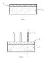
- FIG. 1is a view in cross section of a step of formation of a nucleation layer
- FIG. 4illustrates a representation of the X-ray diffraction spectrum for identifying the types of crystallographic structures present in an Hf-based transition metal layer before nitridation and after nitridation
- FIG. 5represents in detail an implementation of a nitridation step according to one embodiment of the invention
- FIGS. 6 and 7illustrate different steps for preparing a nucleation layer
- FIG. 8illustrates a particular embodiment of a process for manufacturing an optoelectronic device
- the process described belowdiffers from the prior art especially in that the nucleation layer is prepared in two steps, first deposition of a transition metal, followed by at least partial nitridation of this transition metal. This particular sequence of steps makes it possible to give the nucleation layer a better surface intended for growing the nanowires.
- the process for growing at least one semiconductor nanowirecomprises a step of forming, on a substrate 1 , a nucleation layer 2 for the growth of the nanowire and a step of growth of the nanowire 3 ( FIG. 2 ).
- the step of growth of the nanowire 3enables the latter to grow from the nucleation layer 2 .
- An examplehas been given based on the growth of a nanowire, but the growth process is not limited to this sole example and makes it possible, during the growth step, to grow a plurality of nanowires side by side using the nucleation layer 2 .
- the prime function of the nucleation layer 2is to promote the nucleation of the nanowire(s) 3 .
- this nucleation layer 2is preferably chosen so as to protect the substrate 1 from any degradation during the growth (which may be the case if the substrate is made of silicon and the nanowire made of gallium nitride), and/or to conserve good stability at high temperatures (in the case of temperatures above 500° C.), and/or to give good electrical conduction especially when it is desired to polarize each nanowire 3 and to inject current via the substrate 1 .
- the step of formation of the nucleation layercomprises a step of deposition onto the substrate 1 of a layer of a transition metal 4 chosen from Ti (titanium), V (vanadium), Cr (chromium), Zr (zirconium), Nb (niobium), Mo (molybdenum), Hf (hafnium) and Ta (tantalum), followed by a step of nitridation of at least part of the transition metal layer so as to form a layer of transition metal nitride (titanium nitride, vanadium nitride, chromium nitride, zirconium nitride, niobium nitride, molybdenum nitride, hafnium nitride or tantalum nitride, respectively, as a function of the initial transition metal layer deposited) having a surface intended for growing the nanowire(s) 3 .
- this transition metal nitridechosen from Ti (tit
- the transition metal nitride layer thus formedhas growth sites whose crystallographic orientation is more favorable to the growth of nanowires. These growth sites are in greater number and have a better distribution than in the prior art, especially by comparing a titanium nitride nucleation layer prepared according to the process of the invention relative to the titanium nitride layer deposited in a single step of the prior art. In addition, this makes it possible to avoid any formation of a metal-gallium alloy during the growth of gallium-based nanowires. Thus, it is understood that, advantageously, the step of deposition of the said transition metal layer and the nitridation step are performed before the nanowire growth step.
- the nucleation layer 2makes it possible to combine electrical conduction characteristics of metallic type and the refractory nature of a ceramic. These properties, which are in principle antagonist, may be achieved by the transition metals mentioned above.
- the refractory naturemay be achieved by a material whose melting point is associated with a temperature above about 1800° C., which is the case for the transition metal nitrides targeted above.
- Tungstenalthough present in the same column as chromium and molybdenum, is set aside from the list since tungsten nitride has insufficient stability properties at high temperatures, which does not allow efficient growth of the nanowires.
- the transition metal nitride layer thus obtainedalso makes it possible, by virtue of the transition metal used, to have a smaller gap than the AlN-based nucleation layers that have been very commonly used to date as nucleation layer.
- the nucleation layer 2 according to the inventionhas at its interface with the substrate a potential barrier that is easier to cross than in the case where AlN is used, this giving an advantage when it is desired to polarize one or more nanowires from the substrate 1 .
- the step of deposition of the transition metal layeris preferentially performed such that said transition metal layer has, before the nitridation step, at least partly a crystallographic structure of centered cubic (CC) or of hexagonal (these two crystallographic structures are those of the metals mentioned above).
- the cubic-centered (CC) structuremay be obtained naturally by depositing a layer of a transition metal chosen from Cr, Mo, V, Nb, Ta, and the hexagonal structure may be obtained naturally by depositing a layer of a transition metal chosen from Ti, Zr, Hf.
- the specific crystallographic structures targeted previouslymake it possible to perform the step of nitridation of said transition metal layer or at least part of the transition metal layer so as to at least partly modify the crystallographic structure of the transition metal layer toward a face-centered cubic structure, which is especially oriented [111], or hexagonal crystallographic structure, which is especially oriented [0001] or along the direction of the axis “C”, associated with the transition metal nitride layer.
- FIGS. 3 and 4each illustrate an X-ray diffraction spectrum for identifying the crystallographic phases or structures present.
- FIG. 3shows that for the curve C 1 representing the crystallographic structure of the layer of transition metal of Nb type before nitridation, there is indeed a predominance of the orientation [110] of the centered cubic (cc) structure of Nb, and that for the curve C 2 representative of the hexagonal crystallographic structure of the transition metal nitride layer NbN, there is indeed a predominance of the orientation [0004] of the hexagonal structure and of its orientation harmonic [0008], i.e. of similar orientation to [0001].
- FIG. 3shows that for the curve C 1 representing the crystallographic structure of the layer of transition metal of Nb type before nitridation, there is indeed a predominance of the orientation [110] of the centered cubic (cc) structure of Nb, and that for the curve C 2 representative of the hexagonal crystallographic structure of the transition metal nit
- the nitridation stepmay comprise a first substep of nitridation En 1 performed at least partly at a first temperature by imposing an injection of a nitridation gas at a first flow rate, and a second substep of nitridation En 2 performed at least partly at a second temperature less than or equal to the first temperature by imposing an injection of the nitridation gas at a second flow rate, which may or may not be different (i.e. the first flow rate may be equal to the second flow rate), from the first flow rate.
- a second flow ratewhich may or may not be different (i.e. the first flow rate may be equal to the second flow rate)
- the first substep En 1makes it possible to perform a rapid nitridation and the second substep En 2 makes it possible to perform annealing which stabilizes the nitride phase of the transition metal.
- the transition metal nitride layeris chemically and thermally stable and can act as protection for the substrate (in particular if this substrate is made of silicon) during the growth of the nanowire(s).
- the injected gasmay be ammonia NH 3 or dinitrogen N 2 .
- NH 3is preferred since it makes it possible to nitride the transition metal layer more rapidly.
- the nitriding poweris greater than for N 2 . This rapid nitridation may be important especially if the transition metal is capable of being transformed into silicide: this point is addressed hereinbelow.
- the injected nitridation gasbeing ammonia
- the first temperatureis between 1000° C. and 1050° C., especially equal to 1050° C.
- the first flow rateis between 500 sccm and 2500 sccm (sccm means “standard cubic centimeters per minute”), especially equal to 1600 sccm
- the second temperatureis between 950° C. and 1050° C., especially equal to 1000° C.
- the second flow rateis between 500 sccm and 2500 sccm, especially equal to 500 sccm.
- the flow rates mentioned abovecorrespond to the volume capacity of the nitridation chamber used, i.e. a total volume of gas (for example N 2 +NH 3 ) of 8 liters in the example mentioned.
- the flow ratesmust be adapted (for example: for an 18-liter chamber, the first flow rate will especially have to be equal to 4000 sccm and the second flow rate especially equal to 1200 sccm).
- the first flow rateis between 500*V/8 sccm and 2500*V/8 sccm, especially equal to 1600*V/8 sccm
- the second flow rateis between 500*V/8 sccm and 2500*V/8 sccm, especially equal to 500*V/8 sccm.
- Vis the total capacity in liters of a corresponding nitridation chamber.
- corresponding nitridation chambermeans herein the chamber in which the nitridation of the transition metal layer is performed.
- the nitridation stepmay be performed in a nitridation chamber placed at a pressure of between 50 mbar and 800 mbar, especially 100 mbar.
- FIG. 5illustrates in a detailed manner the nitridation step by representing the change in temperature as a function of the time in a nitridation chamber.
- a first time T 1the temperature in the nitridation chamber rises gradually, for example at 2° C./s up to a 1050° C. stage.
- the first nitridation substep under NH 3 En 1 targeted abovebegins when the temperature reaches 200° C. During this first substep, the NH 3 flow rate remains constant at 1600 sccm.
- T 2concomitant with at least part of the first substep, the temperature is maintained at 1050° C. for a time of between 5 minutes and 15 minutes.
- the fifth time T 5may correspond to stoppage of the heating of the chamber and then to its decrease in temperature or may also correspond to a step of growth of the nanowires if the chamber used for the nitridation is also the MOCVD chamber dedicated to the synthesis of the nanowires.
- the step of growth of the nanowire 3is performed after the second nitridation substep En 2 , or is initiated during the second nitridation substep En 2 .
- gallium nitrideto form said at least one nanowire 3 provides at least two advantages.
- a first advantageis that the face-centered cubic or hexagonal structures of the transition metal nitride layer (and thus of the nucleation layer 2 ) are favorable to epitaxy of gallium nitride.
- Nanowires made of gallium nitride, the crystallographic structure of which is a hexagonal structure of the wurtzite type oriented along the axis C (or along the axis [0001]) of FIG. 2may be readily nucleated from the nucleation layer 2 as described.
- the nanowiresmay also be made of ZnO, InN or SiC.
- a second advantageis that gallium nitride is a good candidate with a view of forming an electrooptic device.
- a nanowire 2 made of gallium nitridemakes it possible to form a light nanoemitter.
- GaN-based quantum wellsmay be added either in shell form around the nanowire, or in the continuity of the axis of the nanowire (axial structure).
- the spectral domain of the light emissionmay cover a wide wavelength range extending from ultraviolet to infrared.
- the transition metal layerIn order to achieve optimized nanowire growth, it is preferable for the transition metal layer to be sparingly silicidized/silicide formed. Silicidation of the transition metal layer may arise, if the substrate 1 is based on silicon, according to two cases: during the step of deposition of the transition metal, and/or when it is desired to nitride the deposited transition metal layer to delimit the nucleation layer 2 .
- the first casemay be explained in the following manner.
- silicide compounds MSi 2is promoted (M being the transition metal used).
- Mbeing the transition metal used.
- silicidesonly silicides of transition metals from column V (VSi 2 , NbSi 2 , TaSi 2 ), plus chromium silicide (CrSi 2 ) form crystallographic phases of hexagonal structure, which are potentially advantageous (if textured along the axis c) for the growth of GaN nanowires.
- lattice parameter “a”the disagreement in lattice parameter “a” between these hexagonal phases and GaN (3.19 ⁇ ) is so large, respectively ⁇ 30%, ⁇ 36%, ⁇ 33% and ⁇ 25% for VSi 2 , NbSi 2 , TaSi 2 and CrSi 2 , that epitaxy of GaN is highly improbable.
- the lattice parameter “a” for the hexagonal compounds VSi 2 , NbSi 2 , TaSi 2 and CrSi 2is, respectively: 4.57 ⁇ , 4.97 ⁇ , 4.78 ⁇ and 4.28 ⁇ .
- a subfamilymay be formed from the following materials: Ti, V, Cr, Nb, Ta, Mo, i.e.
- the Nb—Si interdiffusion length over 15 minutesis 12 nm and 2 nm, for 800° C. and 700° C., respectively.
- Nbmay thus be deposited at high temperature up to 700-750° C. without—or with very little—silicidation.
- the other materials: Zr, Hf and Ta having smaller coefficients of interdiffusion with Si than Nb,may thus be readily deposited from room temperature up to 750° C.-800° C. at most. Excessive silicidation would have the consequence of not making it possible later to obtain a transition metal nitride layer of sufficient thickness.
- the nitridation stepwill be optimized.
- the layer 4 that it was sought to produce by depositing a transition metalmay actually comprise a first transition metal silicide layer 5 obtained during the deposition of said transition metal, a second transition metal silicide layer 7 placed in the continuity of the first transition metal silicide layer 5 obtained during the nitridation step and the nucleation layer 2 derived from the nitridation of the layer 6 of FIG. 6 .
- a residual layer 8 of pure transition metalremains intercalated between layer 2 and layer 7 , this depending partly on the initially deposited thickness of the transition metal layer.
- the step of deposition of the transition metal layer 4may comprise a preliminary step of determining the thickness of the transition metal layer 4 to be deposited, said step of determining the thickness comprising: a step of determining a first diffusion length of silicon into the transition metal layer 4 during the future deposition of the transition metal layer as a function of the transition metal used and of the deposition temperature; a step of determining a second diffusion length of silicon into the transition metal layer 4 during the future step of nitridation of the transition metal layer 4 .
- the growth process described abovemay be used in the context of forming an optoelectronic device.
- the inventionmay also relate to a process for manufacturing an optoelectronic device ( FIG. 8 ).
- a manufacturing processcomprises a step of implementing the growth process as has been described above, especially in its various implementations or embodiments.
- the manufacturing processalso comprises a step of electrical doping of a first type of at least one end 3 a of the nanowire 3 opposite the substrate 1 .
- This first typeis, preferably, doping of n type.
- the processalso comprises a step of forming an electrically doped element 9 of a second type opposite the first type at the end 3 a of the nanowire 3 opposite the substrate 1 .
- This second type of dopingis preferentially of p type.
- the end 3 a of the nanowire 3 and the doped element 9 associated with this end 3 amay form a junction of a diode intended to emit light.
- This junctionis preferably a homojunction, i.e. the nanowire 3 and the associated doped element 9 are based on the same materials, for instance gallium nitride.
- the preparation of a heterojunctionis also possible: for example, it is possible to use ZnO in the form of an n-doped nanowire, and then to add quantum wells based on ZnO and to use the element 9 made of electrically p-doped GaN. In point of fact, it is currently difficult to p-dope ZnO.
- the element 9 doped so as to form a junction with the second end 3 a of the nanowire 3may at least partly cover the nanowire 3 at said second end 3 a .
- the doped element 9forms a sheath around the end 3 a of the nanowire 3 .
- the process for manufacturing the optoelectronic devicemay comprise a step of forming quantum wells placed at the interface between the nanowire 3 and the electrically doped element 9 of the second type.
- the quantum wellsmay be deposited in the form of a shell around the nanowire.
- the composition of the material constituting the quantum wellsis adjusted so that the emission of light takes place at the chosen wavelength.
- the quantum wellsare formed in an additional layer sandwiched between the nanowire and the element 9 .
- nanowires associated with the same nucleation surfaceare simultaneously polarized by the nitride layer forming the nucleation layer 2 .
- the electrical resistances of the various transition metals and of their nitridesare correct and in agreement with the literature.
- An advantage of using the transition metal nitrides described hithertois effectively that they allow the nucleation and then growth of GaN nanowires, but another important advantage of these materials is that they do not introduce any potential barrier on the passage of the current (unlike AlN, for example).
- the inventionalso relates to any device obtained via one or other of the processes described above, preferably to any device in which the nucleation layer does not contain titanium.
- the predominant crystallographic structure of the substrateis of orientation [100] at least at the the interface between the substrate and the transition metal layer. This especially makes it possible to reduce the manufacturing costs.
- the temperature T 1is between 400° C. and 1050° C. (or 1400° C.), especially between 500° C. and 800° C. and preferentially equal to 600° C.
- the first substep En 1is divided for the sake of clarity into two steps: step 1 and step 2 .
- a temperature rise up to T 1(i.e. the first temperature) is observed.
- the carrier gasesare N 2 , N 2 +H 2 or H 2 , preferentially N 2 .
- the nitridation gas injectedmay be ammonia (NH 3 ) and the injection may commence at a temperature between room temp. (representative of room temperature) and T 1 ; especially at and above 200° C.
- the temperature increase ramp from room temp. to T 1is greater than 1° C./min, and especially equal to 1° C./sec.
- the ammonia flow ratemay be between 10 ⁇ V/18 sccm and 4000 ⁇ V/18 sccm, especially equal to 1200 ⁇ V/18 sccm (in which V is the volume of the chamber in litres).
- the ratio of the flow rates of ammonia to nitrogen(NH 3 /N 2 ) may be between 0.0005% and 100%, preferably between 0.0055% and 22% and especially equal to 6.6%.
- annealing at T 1is performed.
- the carrier gasesare N 2 , N 2 +H 2 or H 2 , preferentially N 2 .
- the nitridation gas injectedmay be ammonia (NH 3 ).
- the ammonia flow ratemay be between 10 ⁇ V/18 sccm and 4000 ⁇ V/18 sccm, especially equal to 1200 ⁇ V/18 sccm (in which V is the volume of the chamber in litres).
- the ratio of the flow rates of ammonia to nitrogen(NH 3 /N 2 ) may be between 0.0005% and 100%, preferably between 0.0055% and 22% and especially equal to 6.6%.
- the annealing time under NH 3is greater than 1 second, especially between 5 minutes and 30 minutes.
- the second substep En 2is divided for the sake of clarity into three steps: step 3 , step 4 and step 5 .
- the second temperature T 2is between 400° C. and 1050° C. (or 1400° C.), especially between 500° C. and 1000° C. and preferentially equal to 800° C.
- step 3if T 1 ⁇ T 2 , otherwise the process passes directly to step 4 ) there is a temperature rise up to T 2 .
- the carrier gasesare N 2 , N 2 +H 2 or H 2 , preferentially N 2 .
- the nitridation gas injectedmay be ammonia (NH 3 ).
- the temperature increase ramp from up to T 2is greater than 1° C./minute and especially equal to 1° C./sec.
- the ammonia flow ratemay be between 10 ⁇ V/18 sccm and 4000 ⁇ V/18 sccm, especially equal to 1200 ⁇ V/18 sccm (in which V is the volume of the chamber in litres).
- the ratio of the flow rates of ammonia to nitrogen(NH 3 /N 2 ) may be between 0.0005% and 100%, preferably between 0.0055% and 22% and especially equal to 6.6%.
- step 4annealing at T 2 is performed.
- the carrier gasesare N 2 , N 2 +H 2 or H 2 , preferentially N 2 .
- the nitridation gas injectedmay be ammonia (NH 3 ).
- the ammonia flow ratemay be between 10 ⁇ V/18 sccm and 4000 ⁇ V/18 sccm, especially equal to 1200 ⁇ V/18 sccm (in which V is the volume of the chamber in litres).
- the ratio of the flow rates of ammonia to nitrogen(NH 3 /N 2 ) may be between 0.0005% and 100%, preferably between 0.0055% and 22% and especially equal to 6.6%.
- the annealing time under NH 3is greater than 1 second, especially between 1 minute and 30 minutes.
- a temperature decreaseis performed.
- the carrier gasesare N 2 , N 2 +H 2 or H 2 , preferentially N 2 .
- the nitridation gas injectedmay be ammonia (NH 3 ).
- the temperature decrease ramp from T 2 to room temp.is greater than 1° C./min and especially equal to 1° C./sec.
- the ammonia flow ratemay be between 10 ⁇ V/18 sccm and 4000 ⁇ V/18 sccm, especially equal to 1200 ⁇ V/18 sccm (in which V is the volume of the chamber in litres).
- the ratio of the flow rates of ammonia to nitrogen(NH 3 /N 2 ) may be between 0.0005% and 100%, preferably between 0.0055% and 22% and especially equal to 6.6%.
- the nitridation stepmay also be performed in a nitridation chamber placed at a pressure of between 50 mbar and 800 mbar, especially 100 mbar, and the step of growth of the nanowire ( 2 ) may be performed after the second nitridation substep (En 2 ), or is initiated during the second nitridation substep (En 2 ).
- the steps associated with FIG. 5are preferably performed when the transition metal is Ta (in this case the first temperature is preferentially greater than the second temperature during the nitridation step).
- the variant of FIG. 9applies most particularly when it is sought to nitride the transition metal of Ti, Zr, Hf or Nb type (in this case the first temperature is preferentially less than the second temperature during the nitridation step).
- the transition metal depositedis titanium
- the nitridationis performed using a carrier gas which comprises hydrogen, especially in H 2 form. Tests have demonstrated that, in this case, the nanowire growth yield was improved in the presence of hydrogen.
Landscapes
- Engineering & Computer Science (AREA)
- Chemical & Material Sciences (AREA)
- Manufacturing & Machinery (AREA)
- Crystallography & Structural Chemistry (AREA)
- Computer Hardware Design (AREA)
- Microelectronics & Electronic Packaging (AREA)
- Power Engineering (AREA)
- Physics & Mathematics (AREA)
- Condensed Matter Physics & Semiconductors (AREA)
- General Physics & Mathematics (AREA)
- Materials Engineering (AREA)
- Metallurgy (AREA)
- Organic Chemistry (AREA)
- Inorganic Chemistry (AREA)
- Chemical Kinetics & Catalysis (AREA)
- General Chemical & Material Sciences (AREA)
- Nanotechnology (AREA)
- Crystals, And After-Treatments Of Crystals (AREA)
- Chemical Vapour Deposition (AREA)
Abstract
Description
- The invention relates to the field of semiconductor materials and more precisely that of the growth of semiconductor nanowires.
- The invention relates more particularly to a process for growing at least one nanowire.
- In the field of nanowire growth, it is known practice to use nucleation layers such as AlN (aluminum nitride) or TiN (titanium nitride). These layers may be deposited directly by LPCVD (low-pressure chemical vapor deposition) or by APCVD (atmospheric-pressure chemical vapor deposition) as described in document WO 2011/162715.
- This document WO 2011/162715 states that semiconductor nanowires have a growth that may be promoted if the crystallographic orientation of a crystalline substrate enabling the growth is oriented in the direction [111] in a “face-centered cubic structure of NaCl type”, or along the axis “c” in a “hexagonal” structure.
- If the substrate is not correctly oriented, it is possible to deposit an AlN or TiN nucleation layer whose crystallographic structure will have a predominance of orientation in the direction [0001] for AlN which has a hexagonal structure and in the direction [111] for TiN which has a face-centred cubic structure (fcc) structure.
- It results from the foregoing that the crystallographic orientation of the growth support for nanowires is important. The predominance in a correct direction of a crystallographic structure should thus be optimized in order to promote the growth of the nanowires from this crystallographic structure.
- The aim of the present invention is to propose a solution for improving the crystallographic orientation of a nucleation layer of one or more nanowires.
- Steps toward this aim are taken by a process for growing at least one semiconductor nanowire, said growth process comprising a step of forming, on a substrate, a nucleation layer for the growth of the nanowire and a step of growth of the nanowire, in particular the step of forming the nucleation layer comprises the following steps: deposition on the substrate of a layer of a transition metal chosen from Ti, V, Cr, Zr, Nb, Mo, Hf, Ta; nitridation of at least part of the transition metal layer so as to form a layer of transition metal nitride having a surface intended for the growth of the nanowire.
- Advantageously, the nitridation step of said transition metal layer is performed so as to at least partly modify the crystallographic structure of the transition metal layer toward a face-centered cubic crystallographic structure, which is especially oriented [111], or hexagonal crystallographic structure, which is especially oriented [0001] or along the direction of the axis “C”, associated with the transition metal nitride layer.
- According to a particular implementation, the nitridation step comprises: a first nitridation substep at least partly performed at a first temperature by imposing an injection of a nitridation gas at a first flow rate; a second nitridation substep at least partly performed at a second temperature less than or equal to the first temperature by imposing an injection of the nitridation gas at a second flow rate which may or may not be different from the first flow rate. For example, the injected nitridation gas is ammonia, and: the first temperature is between 1000° C. and 1050° C., especially equal to 1050° C.; the first flow rate is between 500*V/8 sccm and 2500*V/8 sccm, especially equal to 1600*V/8 sccm; the second temperature is between 950° C. and 1050° C., especially equal to 1000° C.; the second flow rate is between 500*V/8 sccm and 2500*V/8 sccm, especially equal to 480*V/8 sccm; and in which V is the total capacity in liters of a corresponding nitridation chamber.
- Alternatively, the nitridation step comprises a first nitridation substep at least partly performed at a first temperature by imposing an injection of a nitridation gas at a first flow rate; a second nitridation substep at least partly performed at a second temperature greater than or equal to the first temperature by imposing an injection of the nitridation gas at a second flow rate which may or may not be different from the first flow rate.
- In general, it may be considered that the first temperature may be less than or greater than or equal to the second temperature, and preferably less than or greater than the second temperature.
- According to one implementation, the nitridation step is performed in a nitridation chamber placed at a pressure of between 50 mbar and 800 mbar, especially 100 mbar.
- As an example, the nanowire growth step is performed after the second nitridation substep, or is initiated during the second nitridation substep.
- Preferably, the nanowire growth step comprises a step of injecting Ga so as to form the gallium nitride nanowire, said nanowire extending from the growth surface of the nucleation layer.
- Advantageously, with the substrate being silicon, the step of depositing the transition metal layer is configured such that the interdiffusion of silicon into the deposited transition metal layer is less than 10 nm and/or so as to conserve a non-silicidized slice of the transition metal layer of at least 2 nm.
- In the case where the deposited transition metal is chosen from Cr, V or Ti, said transition metal is deposited at a temperature below 100° C.
- Advantageously, the substrate being based on silicon, the step of depositing the transition metal layer comprises a preliminary step of determining the thickness of the transition metal layer to be deposited, comprising: a step of determining a first diffusion length of the silicon into the transition metal layer during the future deposition of the transition metal layer as a function of the transition metal used and of the deposition temperature; a step of determining a second diffusion length of the silicon into the transition metal layer during the future nitridation step of the transition metal layer; said thickness of the transition metal layer to be deposited being dependent on the desired thickness of the transition metal nitride layer and on a thickness of a silicidized slice of transition metal obtained in the future transition metal layer from the first and second determined diffusion lengths.
- According to one implementation of the growth process, said process comprises a step in which the substrate is envisioned such that it has a resistivity of between 1 mΩ·cm and 100 mΩ·cm.
- Advantageously, the growth process comprises, before deposition of the transition metal layer, a step of deoxidation of a surface of the substrate intended to receive the transition metal layer.
- In addition, the step of depositing said transition metal layer and the nitridation step are preferably implemented before the growth step.
- The invention also relates to a process for manufacturing an optoelectronic device, said process comprising: a step of performing the growth process; the electrical doping of a first type of at least one end of the nanowire which is opposite the substrate; the formation of an electrically doped element of a second type opposite the first type at the end of the nanowire opposite the substrate. In addition, such a process may also comprise a step of forming quantum wells placed at the interface between the nanowire and the electrically doped element of the second type.
- Other advantages and characteristics will emerge more clearly from the description which follows of particular embodiments of the invention, which are given as nonlimiting examples and represented on the attached drawings, in which:
FIG. 1 is a view in cross section of a step of formation of a nucleation layer,FIG. 2 is a view in cross section of a step of nucleation of at least one nanowire from the nucleation layer,FIG. 3 illustrates a representation of the X-ray diffraction spectrum for identifying the types of crystallographic structures present in an Nb-based transition metal layer before nitridation and after nitridation,FIG. 4 illustrates a representation of the X-ray diffraction spectrum for identifying the types of crystallographic structures present in an Hf-based transition metal layer before nitridation and after nitridation,FIG. 5 represents in detail an implementation of a nitridation step according to one embodiment of the invention,FIGS. 6 and 7 illustrate different steps for preparing a nucleation layer,FIG. 8 illustrates a particular embodiment of a process for manufacturing an optoelectronic device,FIG. 9 illustrates in detail another implementation of a nitridation step according to one embodiment of the invention.- The process described below differs from the prior art especially in that the nucleation layer is prepared in two steps, first deposition of a transition metal, followed by at least partial nitridation of this transition metal. This particular sequence of steps makes it possible to give the nucleation layer a better surface intended for growing the nanowires.
- The term “microwire” or “nanowire” in the rest of the description preferentially means a three-dimensional structure of elongated shape whose longitudinal dimension is at least equal to once the transverse dimension(s), preferably at least five times and even more preferentially at least ten times. The transverse dimension(s) are between 5 nm and 2.5 μm. In certain embodiments, the transverse dimensions may be less than or equal to about 1 μm, preferably between 100 nm and 300 nm. In certain embodiments, the height of each nanowire may be greater than or equal to 500 nm, preferably between 1 μm and 50 μm.
- As illustrated in
FIG. 1 , the process for growing at least one semiconductor nanowire comprises a step of forming, on asubstrate 1, anucleation layer 2 for the growth of the nanowire and a step of growth of the nanowire3 (FIG. 2 ). Needless to say, the step of growth of thenanowire 3 enables the latter to grow from thenucleation layer 2. - An example has been given based on the growth of a nanowire, but the growth process is not limited to this sole example and makes it possible, during the growth step, to grow a plurality of nanowires side by side using the
nucleation layer 2. - It is understood from the foregoing that the prime function of the
nucleation layer 2 is to promote the nucleation of the nanowire(s)3. In addition, thisnucleation layer 2 is preferably chosen so as to protect thesubstrate 1 from any degradation during the growth (which may be the case if the substrate is made of silicon and the nanowire made of gallium nitride), and/or to conserve good stability at high temperatures (in the case of temperatures above 500° C.), and/or to give good electrical conduction especially when it is desired to polarize eachnanowire 3 and to inject current via thesubstrate 1. - As regards the
substrate 1, the process may, in a nonlimiting manner, comprise a step in which the substrate is provided such that it has a resistivity of between 1 mΩ·cm and 100 mΩ·cm. This resistivity is advantageous when it is desired to polarize the nanowires as indicated above across thenucleation layer 2. - To begin with, it should be noted that a
nucleation layer 2 makes it possible to promote the growth of one ormore nanowires 3 when these wires grow from thisnucleation layer 2 in the vast majority substantially perpendicular to the substrate1 (axis C represented inFIG. 2 ). The term “substantially perpendicular to” means exactly perpendicular or perpendicular to more or less 10°. This slight disorientation of more or less 10° nevertheless permits the performance of subsequent technological steps for preparing more complete devices. - It will thus be sought to have, in the nucleation layer, a crystallographic orientation adapted to the growth of the
nanowires 3. Moreover, if this crystallographic orientation is dense, i.e. predominant, the density of thesenanowires 3 can then be magnified. - For this, the step of formation of the nucleation layer comprises a step of deposition onto the
substrate 1 of a layer of atransition metal 4 chosen from Ti (titanium), V (vanadium), Cr (chromium), Zr (zirconium), Nb (niobium), Mo (molybdenum), Hf (hafnium) and Ta (tantalum), followed by a step of nitridation of at least part of the transition metal layer so as to form a layer of transition metal nitride (titanium nitride, vanadium nitride, chromium nitride, zirconium nitride, niobium nitride, molybdenum nitride, hafnium nitride or tantalum nitride, respectively, as a function of the initial transition metal layer deposited) having a surface intended for growing the nanowire(s)3. In order to optimize the growth, this transition metal nitride layer may have a minimum thickness of 2 nm and preferably between 2 nm and 50 nm. - According to one embodiment, the deposition of the transition metal layer is performed at a temperature between room temperature and 400° C. Beyond this temperature, there is a risk of lowering of the nanowire growth yield.
- According to one implementation applicable to the different transition metals, especially for Hf, Nb and Ta, the deposited transition metal layer may have a thickness of between 20 nm and a few hundred nanometers (for example 200 nm). For the other transition metals, a thickness of nm will be preferred. The deposition may be performed by PVD (physical vapor deposition) from a metal target, for example a continuous-current spray passing over the target. During this step of deposition of the transition metal, the
substrate 1 may be maintained at room temperature. In a general manner applicable throughout the description, the term “room temperature” means a temperature preferably between 20° C. and 50° C. The pressure in the PVD chamber during the deposition of the transition metal may be between 3×10⁻³mbar and 6×10⁻³mbar. - After various tests, it was possible to observe that the growth of nanowire(s) was promoted by this
nucleation layer 2 formed in two steps. - In point of fact, it turns out that the transition metal nitride layer thus formed has growth sites whose crystallographic orientation is more favorable to the growth of nanowires. These growth sites are in greater number and have a better distribution than in the prior art, especially by comparing a titanium nitride nucleation layer prepared according to the process of the invention relative to the titanium nitride layer deposited in a single step of the prior art. In addition, this makes it possible to avoid any formation of a metal-gallium alloy during the growth of gallium-based nanowires. Thus, it is understood that, advantageously, the step of deposition of the said transition metal layer and the nitridation step are performed before the nanowire growth step.
- Furthermore, the fact of choosing one of the following transition metals: Ti, V, Cr, Zr, Nb, Mo, Hf, Ta, to form, after nitridation of the said transition metal, the
nucleation layer 2 makes it possible to combine electrical conduction characteristics of metallic type and the refractory nature of a ceramic. These properties, which are in principle antagonist, may be achieved by the transition metals mentioned above. In point of fact, the refractory nature may be achieved by a material whose melting point is associated with a temperature above about 1800° C., which is the case for the transition metal nitrides targeted above. Tungsten, although present in the same column as chromium and molybdenum, is set aside from the list since tungsten nitride has insufficient stability properties at high temperatures, which does not allow efficient growth of the nanowires. - The transition metal nitride layer thus obtained also makes it possible, by virtue of the transition metal used, to have a smaller gap than the AlN-based nucleation layers that have been very commonly used to date as nucleation layer. Thus, when the
substrate 1 is based on silicon, thenucleation layer 2 according to the invention has at its interface with the substrate a potential barrier that is easier to cross than in the case where AlN is used, this giving an advantage when it is desired to polarize one or more nanowires from thesubstrate 1. - It results from the foregoing that the crystallographic orientation of the
nucleation layer 2, especially on a surface intended for growing the nanowire(s), is of importance in the context of promoting the growth of nanowire(s). Thus, the step of deposition of the transition metal layer is preferentially performed such that said transition metal layer has, before the nitridation step, at least partly a crystallographic structure of centered cubic (CC) or of hexagonal (these two crystallographic structures are those of the metals mentioned above). - In the present description, when predominance of a crystallographic structure is mentioned, this means that said structure appears in greater proportion than each of the other crystallographic structures taken independently.
- Typically, for the transition metals targeted above, the cubic-centered (CC) structure may be obtained naturally by depositing a layer of a transition metal chosen from Cr, Mo, V, Nb, Ta, and the hexagonal structure may be obtained naturally by depositing a layer of a transition metal chosen from Ti, Zr, Hf.
- The specific crystallographic structures targeted previously make it possible to perform the step of nitridation of said transition metal layer or at least part of the transition metal layer so as to at least partly modify the crystallographic structure of the transition metal layer toward a face-centered cubic structure, which is especially oriented [111], or hexagonal crystallographic structure, which is especially oriented [0001] or along the direction of the axis “C”, associated with the transition metal nitride layer.
FIGS. 3 and 4 each illustrate an X-ray diffraction spectrum for identifying the crystallographic phases or structures present.FIG. 3 shows that for the curve C1 representing the crystallographic structure of the layer of transition metal of Nb type before nitridation, there is indeed a predominance of the orientation [110] of the centered cubic (cc) structure of Nb, and that for the curve C2 representative of the hexagonal crystallographic structure of the transition metal nitride layer NbN, there is indeed a predominance of the orientation [0004] of the hexagonal structure and of its orientation harmonic [0008], i.e. of similar orientation to [0001].FIG. 4 shows that for the curve C3 representative of the hexagonal crystallographic structure of the transition metal layer of Hf type before nitridation, there is indeed a predominance of the orientation [0002] of the hexagonal structure, and that for the curve C4 representative of the face-centered cubic crystallographic structure of the transition metal nitride layer HfN, there is indeed a predominance of the orientation [111] of the face-centered cubic structure. OnFIGS. 3 and 4 , only the peaks are important for visualizing the predominance, the rest of the curve representing a continuous background due to the experimental device and the sample. Similar curves may be produced by a person skilled in the art for the other transition metals and the conclusions would be substantially identical, for example for tantalum nitride, there would be a predominance of the orientation [111] of the face-centered cubic structure of tantalum nitride.- According to a particular implementation, especially illustrated in
FIG. 5 , the nitridation step may comprise a first substep of nitridation En1 performed at least partly at a first temperature by imposing an injection of a nitridation gas at a first flow rate, and a second substep of nitridation En2 performed at least partly at a second temperature less than or equal to the first temperature by imposing an injection of the nitridation gas at a second flow rate, which may or may not be different (i.e. the first flow rate may be equal to the second flow rate), from the first flow rate. This makes it possible to optimize the crystallographic orientation of the nucleation layer. It goes without saying that these two nitridation substeps are performed one after the other. In particular, the first substep En1 makes it possible to perform a rapid nitridation and the second substep En2 makes it possible to perform annealing which stabilizes the nitride phase of the transition metal. Following these two substeps En1 and En2, the transition metal nitride layer is chemically and thermally stable and can act as protection for the substrate (in particular if this substrate is made of silicon) during the growth of the nanowire(s). - The injected gas may be ammonia NH3or dinitrogen N2. NH3is preferred since it makes it possible to nitride the transition metal layer more rapidly. In point of fact, in the NH3form, the nitriding power is greater than for N2. This rapid nitridation may be important especially if the transition metal is capable of being transformed into silicide: this point is addressed hereinbelow.
- According to a particular example, the injected nitridation gas being ammonia, the first temperature is between 1000° C. and 1050° C., especially equal to 1050° C., the first flow rate is between 500 sccm and 2500 sccm (sccm means “standard cubic centimeters per minute”), especially equal to 1600 sccm, the second temperature is between 950° C. and 1050° C., especially equal to 1000° C., the second flow rate is between 500 sccm and 2500 sccm, especially equal to 500 sccm.
- The flow rates mentioned above correspond to the volume capacity of the nitridation chamber used, i.e. a total volume of gas (for example N2+NH3) of 8 liters in the example mentioned. For a chamber of a different volume, the flow rates must be adapted (for example: for an 18-liter chamber, the first flow rate will especially have to be equal to 4000 sccm and the second flow rate especially equal to 1200 sccm). In other words, the first flow rate is between 500*V/8 sccm and 2500*V/8 sccm, especially equal to 1600*V/8 sccm, and the second flow rate is between 500*V/8 sccm and 2500*V/8 sccm, especially equal to 500*V/8 sccm. V is the total capacity in liters of a corresponding nitridation chamber. The term “corresponding nitridation chamber” means herein the chamber in which the nitridation of the transition metal layer is performed.
- In general, the nitridation step may be performed in a nitridation chamber placed at a pressure of between 50 mbar and 800 mbar, especially 100 mbar.
FIG. 5 illustrates in a detailed manner the nitridation step by representing the change in temperature as a function of the time in a nitridation chamber. In a first time T1, the temperature in the nitridation chamber rises gradually, for example at 2° C./s up to a 1050° C. stage. The first nitridation substep under NH3En1 targeted above begins when the temperature reaches 200° C. During this first substep, the NH3flow rate remains constant at 1600 sccm. In a second time T2, concomitant with at least part of the first substep, the temperature is maintained at 1050° C. for a time of between 5 minutes and 15 minutes. In a third time T3, the first substep En1 is continued while the temperature passes from 1050° C. to 1000° C. in 60 s. In a fourth time T4, the temperature in the nitridation chamber is maintained at 1000° C. for a time of between 5 minutes and 15 minutes and the second substep En2 is started. In a fifth time T5, the introduction of heat into the nitridation chamber is stopped so that the temperature of the nitridation chamber falls until it returns to room temperature. The duration of T5 may correspond to the inertia of the nitridation chamber. The second nitridation substep En2 may be continued for a given time during the fifth time T5. The fifth time T5 may correspond to stoppage of the heating of the chamber and then to its decrease in temperature or may also correspond to a step of growth of the nanowires if the chamber used for the nitridation is also the MOCVD chamber dedicated to the synthesis of the nanowires. According to a particular implementation, the step of growth of thenanowire 3 is performed after the second nitridation substep En2, or is initiated during the second nitridation substep En2.- In general, the step of growth of said at least one
nanowire 3 may comprise a step of injecting a material intended at least partly to form thenanowire 3. In particular, this will be an injection of Ga so as to form thegallium nitride nanowire 3, saidnanowire 3 extending from the growth surface of thenucleation layer 2. To form the gallium nitride nanowire, the injection of Ga may be performed concomitantly with an injection of NH3or N2. In general, for the synthesis of GaN, it is the reaction of Ga with NH3and not with N2that is used. The injection of Ga may be performed in a chamber adapted to the growth of nanowires. - The use of gallium nitride to form said at least one
nanowire 3 provides at least two advantages. - A first advantage is that the face-centered cubic or hexagonal structures of the transition metal nitride layer (and thus of the nucleation layer2) are favorable to epitaxy of gallium nitride. Nanowires made of gallium nitride, the crystallographic structure of which is a hexagonal structure of the wurtzite type oriented along the axis C (or along the axis [0001]) of
FIG. 2 , may be readily nucleated from thenucleation layer 2 as described. Alternatively, the nanowires may also be made of ZnO, InN or SiC. - A second advantage is that gallium nitride is a good candidate with a view of forming an electrooptic device. Specifically, such a
nanowire 2 made of gallium nitride makes it possible to form a light nanoemitter. GaN-based quantum wells may be added either in shell form around the nanowire, or in the continuity of the axis of the nanowire (axial structure). Depending on the composition of these GaN-based quantum wells, the spectral domain of the light emission may cover a wide wavelength range extending from ultraviolet to infrared. - In order to achieve optimized nanowire growth, it is preferable for the transition metal layer to be sparingly silicidized/silicide formed. Silicidation of the transition metal layer may arise, if the
substrate 1 is based on silicon, according to two cases: during the step of deposition of the transition metal, and/or when it is desired to nitride the deposited transition metal layer to delimit thenucleation layer 2. - The first case may be explained in the following manner. In point of fact, at high temperature (about 1000° C.), the formation of silicide compounds MSi2is promoted (M being the transition metal used). Among these silicides, only silicides of transition metals from column V (VSi2, NbSi2, TaSi2), plus chromium silicide (CrSi2) form crystallographic phases of hexagonal structure, which are potentially advantageous (if textured along the axis c) for the growth of GaN nanowires. However, the disagreement in lattice parameter “a” between these hexagonal phases and GaN (3.19 Å) is so large, respectively −30%, −36%, −33% and −25% for VSi2, NbSi2, TaSi2and CrSi2, that epitaxy of GaN is highly improbable. Typically, the lattice parameter “a” for the hexagonal compounds VSi2, NbSi2, TaSi2and CrSi2is, respectively: 4.57 Å, 4.97 Å, 4.78 Å and 4.28 Å. Thus, a subfamily may be formed from the following materials: Ti, V, Cr, Nb, Ta, Mo, i.e. metals for which the interdiffusion coefficient with Si is high, which implies rapid growth kinetics of the new MSi2phase. By way of example, Cr has a coefficient of interdiffusion with Si at 850° C. of 1.5×10⁻⁷ cm2/s, i.e. a diffusion length of about 11.6 μm in 15 minutes, whereas at about 100° C., this diffusion length falls to about 80 nm in 15 minutes. For the reasons mentioned above, if the deposited transition metal is chosen from Cr, V and Ti, it is preferentially deposited at a temperature below 100° C. so as to limit the diffusion of the silicon derived from the substrate. For Nb, the Nb—Si interdiffusion length over 15 minutes is 12 nm and 2 nm, for 800° C. and 700° C., respectively. Nb may thus be deposited at high temperature up to 700-750° C. without—or with very little—silicidation. The other materials: Zr, Hf and Ta having smaller coefficients of interdiffusion with Si than Nb, may thus be readily deposited from room temperature up to 750° C.-800° C. at most. Excessive silicidation would have the consequence of not making it possible later to obtain a transition metal nitride layer of sufficient thickness. In other words, to generalize, when the substrate is silicon, the step of deposition of the transition metal layer is configured such that the interdiffusion of silicon into the deposited transition metal layer is less than 10 nm and/or so as to conserve a non-silicidized slice of the transition metal layer of at least 2 nm. In point of fact, this non-silicidized slice is opposite the substrate and is intended to form the nitride layer of the transition metal.
- In
FIG. 6 ,reference 4 indicates the transition metal layer initially deposited on thesubstrate 1, during the deposition of thelayer 4, a slice of this layer may be silicidized such that only part6 of thelayer 4 is composed of the pure transition metal that can serve to form, by nitridation, the nucleation layer. - In the second case, the nitridation step may make it necessary to work at 1050° C. for a few minutes. To do this, use will preferably be made as nitriding gas of NH3, since, by virtue of its high nitriding power, the nitridation reaction rate is higher than the silicidation reaction rate. In point of fact, in the ideal case, it is sought to form (
FIG. 7 ) during the nitridation step at least one transition metal nitride layer2 (i.e. the nucleation layer) in the depositedtransition metal layer 4, the thickness of said transition metal nitride layer advantageously being between 2 nm and 50 nm. In order to avoid the production of a large amount of a new silicide compound in the region of this transition metal nitride layer, the nitridation step will be optimized. In point of fact, after the nitridation step, it is understood, as illustrated inFIG. 7 , that thelayer 4 that it was sought to produce by depositing a transition metal may actually comprise a first transitionmetal silicide layer 5 obtained during the deposition of said transition metal, a second transition metal silicide layer7 placed in the continuity of the first transitionmetal silicide layer 5 obtained during the nitridation step and thenucleation layer 2 derived from the nitridation of the layer6 ofFIG. 6 . Optionally, it is also possible that a residual layer8 of pure transition metal remains intercalated betweenlayer 2 and layer7, this depending partly on the initially deposited thickness of the transition metal layer. - It results from the explanation of the first and second cases that if the
substrate 1 is made of silicon, a person skilled in the art will be capable of determining the thickness of the transition metal layer which is sought to be deposited as a function of the type of transition metal to be deposited, of the temperature of deposition of the transition metal, of the duration of the transition metal deposition, and also of the duration of the nitridation step so that it is possible to obtain a layer of transition metal nitride of a predetermined thickness. In other words, for a substrate based on silicon, the step of deposition of thetransition metal layer 4 may comprise a preliminary step of determining the thickness of thetransition metal layer 4 to be deposited, said step of determining the thickness comprising: a step of determining a first diffusion length of silicon into thetransition metal layer 4 during the future deposition of the transition metal layer as a function of the transition metal used and of the deposition temperature; a step of determining a second diffusion length of silicon into thetransition metal layer 4 during the future step of nitridation of thetransition metal layer 4. Said thickness of thetransition metal layer 4 to be deposited being a function of the desired thickness of the transition metal nitride layer and of a thickness of a silicidized slice of transition metal obtained in the futuretransition metal layer 4 from the first and second determined diffusion lengths. - In general, the
substrate 1 will advantageously be prepared before the deposition of thetransition metal layer 4. To do this, the process may comprise, before the step of deposition of the transition metal layer, a step of deoxidation of a surface of thesubstrate 1 intended to receive the deposit of thetransition metal layer 4. More particularly, this step of deoxidation of the surface of the silicon may be performed either chemically (HF bath) or physically (etching of the surface by applying a bias tension to the substrate1). This makes it possible especially to remove the layer of native silicon oxide (SiO2) which is an “insulating” barrier to the injection of electrons into the nucleation layer and into the gallium nitride nanowire. - Preferentially, the growth process described above may be used in the context of forming an optoelectronic device.
- Thus, the invention may also relate to a process for manufacturing an optoelectronic device (
FIG. 8 ). Such a manufacturing process comprises a step of implementing the growth process as has been described above, especially in its various implementations or embodiments. Moreover, the manufacturing process also comprises a step of electrical doping of a first type of at least oneend 3aof thenanowire 3 opposite thesubstrate 1. This first type is, preferably, doping of n type. In addition, the process also comprises a step of forming an electrically doped element9 of a second type opposite the first type at theend 3aof thenanowire 3 opposite thesubstrate 1. This second type of doping is preferentially of p type. Thus, theend 3aof thenanowire 3 and the doped element9 associated with thisend 3amay form a junction of a diode intended to emit light. This junction is preferably a homojunction, i.e. thenanowire 3 and the associated doped element9 are based on the same materials, for instance gallium nitride. The preparation of a heterojunction is also possible: for example, it is possible to use ZnO in the form of an n-doped nanowire, and then to add quantum wells based on ZnO and to use the element9 made of electrically p-doped GaN. In point of fact, it is currently difficult to p-dope ZnO. FIG. 8 illustrates a particular example of the optoelectronic device obtained from the manufacturing process. It thus features thesubstrate 1, preferably made of silicon and configured so as to be electrically conductive (for example n-doped), one face of thesubstrate 1 is oriented toward thenucleation layer 2. From thisnucleation layer 2 extends thenanowire 3. The term “extends” means that thenanowire 3 has a length defined between twolongitudinal ends longitudinal end 3bbeing in contact with thenucleation layer 2 and a secondlongitudinal end 3abeing distant from thenucleation layer 2. The element9 doped so as to form a junction with thesecond end 3aof thenanowire 3 may at least partly cover thenanowire 3 at saidsecond end 3a. Preferably, the doped element9 forms a sheath around theend 3aof thenanowire 3.- Moreover, in the context of an optoelectronic device, it may be advantageous to add quantum wells intended to form confinement zones so as to increase the emission yield of the
nanowire 3. Thus, the process for manufacturing the optoelectronic device may comprise a step of forming quantum wells placed at the interface between thenanowire 3 and the electrically doped element9 of the second type. The quantum wells may be deposited in the form of a shell around the nanowire. The composition of the material constituting the quantum wells is adjusted so that the emission of light takes place at the chosen wavelength. The quantum wells are formed in an additional layer sandwiched between the nanowire and the element9. - Preferably, nanowires associated with the same nucleation surface are simultaneously polarized by the nitride layer forming the
nucleation layer 2. By using a sparinglyresistive silicon substrate 1, the electrical resistances of the various transition metals and of their nitrides are correct and in agreement with the literature. An advantage of using the transition metal nitrides described hitherto is effectively that they allow the nucleation and then growth of GaN nanowires, but another important advantage of these materials is that they do not introduce any potential barrier on the passage of the current (unlike AlN, for example). - The invention also relates to any device obtained via one or other of the processes described above, preferably to any device in which the nucleation layer does not contain titanium.
- Preferably, the predominant crystallographic structure of the substrate is of orientation [100] at least at the the interface between the substrate and the transition metal layer. This especially makes it possible to reduce the manufacturing costs.
- According to an alternative to the embodiment of
FIG. 5 , the nitridation step comprises a first nitridation substep En1 performed at least partly at a first temperature by imposing an injection of a nitridation gas at a first flow rate, a second nitridation substep En2 performed at least partly at a second temperature greater than or equal to the first temperature by imposing an injection of the nitridation gas at a second flow rate, which may or may not be different (i.e. the first flow rate may be equal to the second flow rate) from the first flow rate. - This alternative of
FIG. 5 is illustrated inFIG. 9 . Thus, inFIG. 9 , the temperature T1 is between 400° C. and 1050° C. (or 1400° C.), especially between 500° C. and 800° C. and preferentially equal to 600° C. - The first substep En1 is divided for the sake of clarity into two steps:
step 1 andstep 2. - In
step 1 ofFIG. 9 , a temperature rise up to T1 (i.e. the first temperature) is observed. The carrier gases are N2, N2+H2or H2, preferentially N2. The nitridation gas injected may be ammonia (NH3) and the injection may commence at a temperature between room temp. (representative of room temperature) and T1; especially at and above 200° C. The temperature increase ramp from room temp. to T1 is greater than 1° C./min, and especially equal to 1° C./sec. During thisstep 1, the ammonia flow rate may be between 10×V/18 sccm and 4000×V/18 sccm, especially equal to 1200×V/18 sccm (in which V is the volume of the chamber in litres). In general, the ratio of the flow rates of ammonia to nitrogen (NH3/N2) may be between 0.0005% and 100%, preferably between 0.0055% and 22% and especially equal to 6.6%. - In
step 2 ofFIG. 9 , annealing at T1 is performed. The carrier gases are N2, N2+H2or H2, preferentially N2. The nitridation gas injected may be ammonia (NH3). The ammonia flow rate may be between 10×V/18 sccm and 4000×V/18 sccm, especially equal to 1200×V/18 sccm (in which V is the volume of the chamber in litres). In general, the ratio of the flow rates of ammonia to nitrogen (NH3/N2) may be between 0.0005% and 100%, preferably between 0.0055% and 22% and especially equal to 6.6%. Preferably, the annealing time under NH3is greater than 1 second, especially between 5 minutes and 30 minutes. - The second substep En2 is divided for the sake of clarity into three steps:
step 3,step 4 andstep 5. Preferably, the second temperature T2 is between 400° C. and 1050° C. (or 1400° C.), especially between 500° C. and 1000° C. and preferentially equal to 800° C. In step3 (if T1≠T2, otherwise the process passes directly to step4) there is a temperature rise up to T2. The carrier gases are N2, N2+H2or H2, preferentially N2. The nitridation gas injected may be ammonia (NH3). The temperature increase ramp from up to T2 is greater than 1° C./minute and especially equal to 1° C./sec. The ammonia flow rate may be between 10×V/18 sccm and 4000×V/18 sccm, especially equal to 1200×V/18 sccm (in which V is the volume of the chamber in litres). In general, the ratio of the flow rates of ammonia to nitrogen (NH3/N2) may be between 0.0005% and 100%, preferably between 0.0055% and 22% and especially equal to 6.6%. - In
step 4, annealing at T2 is performed. The carrier gases are N2, N2+H2or H2, preferentially N2. The nitridation gas injected may be ammonia (NH3). The ammonia flow rate may be between 10×V/18 sccm and 4000×V/18 sccm, especially equal to 1200×V/18 sccm (in which V is the volume of the chamber in litres). In general, the ratio of the flow rates of ammonia to nitrogen (NH3/N2) may be between 0.0005% and 100%, preferably between 0.0055% and 22% and especially equal to 6.6%. The annealing time under NH3is greater than 1 second, especially between 1 minute and 30 minutes. - In
step 5, a temperature decrease is performed. The carrier gases are N2, N2+H2or H2, preferentially N2. The nitridation gas injected may be ammonia (NH3). The temperature decrease ramp from T2 to room temp. is greater than 1° C./min and especially equal to 1° C./sec. The ammonia flow rate may be between 10×V/18 sccm and 4000×V/18 sccm, especially equal to 1200×V/18 sccm (in which V is the volume of the chamber in litres). In general, the ratio of the flow rates of ammonia to nitrogen (NH3/N2) may be between 0.0005% and 100%, preferably between 0.0055% and 22% and especially equal to 6.6%. - As regards this alternative of
FIG. 9 , the nitridation step may also be performed in a nitridation chamber placed at a pressure of between 50 mbar and 800 mbar, especially 100 mbar, and the step of growth of the nanowire (2) may be performed after the second nitridation substep (En2), or is initiated during the second nitridation substep (En2). - The steps associated with
FIG. 5 are preferably performed when the transition metal is Ta (in this case the first temperature is preferentially greater than the second temperature during the nitridation step). - Specifically, for this material, an appreciable improvement is obtained in the quality of the nanowires obtained (verticality, shape homogeneity) relative to the variant of
FIG. 9 . Conversely, and for the same reasons, the variant ofFIG. 9 applies most particularly when it is sought to nitride the transition metal of Ti, Zr, Hf or Nb type (in this case the first temperature is preferentially less than the second temperature during the nitridation step). - Advantageously, and in a manner applicable to everything that has been stated above, when the transition metal deposited is titanium, the nitridation is performed using a carrier gas which comprises hydrogen, especially in H2form. Tests have demonstrated that, in this case, the nanowire growth yield was improved in the presence of hydrogen.
Claims (20)
Applications Claiming Priority (3)
| Application Number | Priority Date | Filing Date | Title |
|---|---|---|---|
| FR1260208AFR2997420B1 (en) | 2012-10-26 | 2012-10-26 | PROCESS FOR GROWING AT LEAST ONE NANOFIL FROM A TWO-STEP NITRIDE TRANSITION METAL LAYER |
| FR1260208 | 2012-10-26 | ||
| PCT/EP2013/072424WO2014064263A2 (en) | 2012-10-26 | 2013-10-25 | Method for growing at least one nanowire from a layer of a transition nitride metal, said layer being obtained in two steps |
Publications (2)
| Publication Number | Publication Date |
|---|---|
| US20150279672A1true US20150279672A1 (en) | 2015-10-01 |
| US10636653B2 US10636653B2 (en) | 2020-04-28 |
Family
ID=47666274
Family Applications (2)
| Application Number | Title | Priority Date | Filing Date |
|---|---|---|---|
| US14/438,480ActiveUS10636653B2 (en) | 2012-10-26 | 2013-10-25 | Process for growing at least one nanowire using a transition metal nitride layer obtained in two steps |
| US14/064,916ActiveUS9698011B2 (en) | 2012-10-26 | 2013-10-28 | Process for growing at least one nanowire using a transition metal nitride layer obtained in two steps |
Family Applications After (1)
| Application Number | Title | Priority Date | Filing Date |
|---|---|---|---|
| US14/064,916ActiveUS9698011B2 (en) | 2012-10-26 | 2013-10-28 | Process for growing at least one nanowire using a transition metal nitride layer obtained in two steps |
Country Status (8)
| Country | Link |
|---|---|
| US (2) | US10636653B2 (en) |
| EP (3) | EP3719849A3 (en) |
| JP (1) | JP6367208B2 (en) |
| KR (1) | KR102134495B1 (en) |
| CN (1) | CN104871317B (en) |
| BR (1) | BR112015009308B1 (en) |
| FR (1) | FR2997420B1 (en) |
| WO (1) | WO2014064263A2 (en) |
Cited By (6)
| Publication number | Priority date | Publication date | Assignee | Title |
|---|---|---|---|---|
| US20170047477A1 (en)* | 2014-04-22 | 2017-02-16 | Commissariat A L'energie Atomique Et Aux Energies Alternatives | Optoelectronic device with improved light extraction efficiency |
| US9679966B2 (en) | 2012-10-26 | 2017-06-13 | Commissariat A L'energie Atomique Et Aux Energies Alternatives | Electronic device containing nanowire(s), equipped with a transition metal buffer layer, process for growing at least one nanowire, and process for manufacturing a device |
| US9698011B2 (en) | 2012-10-26 | 2017-07-04 | Commissariat A L'energie Atomique Et Aux Energies Alternatives | Process for growing at least one nanowire using a transition metal nitride layer obtained in two steps |
| US10312081B2 (en) | 2016-07-15 | 2019-06-04 | University Of Kentucky Research Foundation | Synthesis of metal oxide surfaces and interfaces with crystallographic control using solid-liquid-vapor etching and vapor-liquid-solid growth |
| US10340138B2 (en) | 2014-12-05 | 2019-07-02 | Commissariat A L'energie Atomique Et Aux Energies Alternatives | Electronic device with a wire element extending from an electroconductive layer comprising zirconium carbide or hafnium carbide |
| WO2023064157A1 (en)* | 2021-10-14 | 2023-04-20 | Applied Materials, Inc. | SUBSTRATE PROCESSING FOR GaN GROWTH |
Families Citing this family (5)
| Publication number | Priority date | Publication date | Assignee | Title |
|---|---|---|---|---|
| US10714350B2 (en)* | 2016-11-01 | 2020-07-14 | ASM IP Holdings, B.V. | Methods for forming a transition metal niobium nitride film on a substrate by atomic layer deposition and related semiconductor device structures |
| FR3082657B1 (en)* | 2018-06-19 | 2021-01-29 | Aledia | MANUFACTURING PROCESS OF AN OPTOELECTRONIC DEVICE WITH SELF-ALIGNED LUMINOUS CONTAINMENT WALLS |
| KR102357733B1 (en) | 2019-12-18 | 2022-02-04 | 덕산하이메탈(주) | Conductive layer and manufacturing method thereof |
| KR20210078634A (en) | 2019-12-18 | 2021-06-29 | 덕산하이메탈(주) | Metal nanowire and Method of manufacturing thereof |
| CN116314507B (en)* | 2023-05-19 | 2023-07-28 | 江西兆驰半导体有限公司 | Light-emitting diode epitaxial wafer and preparation method thereof, light-emitting diode |
Citations (30)
| Publication number | Priority date | Publication date | Assignee | Title |
|---|---|---|---|---|
| US5254499A (en)* | 1992-07-14 | 1993-10-19 | Micron Technology, Inc. | Method of depositing high density titanium nitride films on semiconductor wafers |
| US5593511A (en)* | 1994-06-03 | 1997-01-14 | Sony Corporation | Method of nitridization of titanium thin films |
| US5628829A (en)* | 1994-06-03 | 1997-05-13 | Materials Research Corporation | Method and apparatus for low temperature deposition of CVD and PECVD films |
| US6093645A (en)* | 1997-02-10 | 2000-07-25 | Tokyo Electron Limited | Elimination of titanium nitride film deposition in tungsten plug technology using PE-CVD-TI and in-situ plasma nitridation |
| US20010001954A1 (en)* | 1997-12-02 | 2001-05-31 | Koji Urabe | Apparatus and method for manufacturing semiconductor device |
| US6447838B1 (en)* | 1993-12-10 | 2002-09-10 | Symetrix Corporation | Integrated circuit capacitors with barrier layer and process for making the same |
| US20030102444A1 (en)* | 2000-05-04 | 2003-06-05 | Deppert Knut Wilfried | Nanostructures |
| US6617060B2 (en)* | 2000-12-14 | 2003-09-09 | Nitronex Corporation | Gallium nitride materials and methods |
| WO2004004927A2 (en)* | 2002-07-08 | 2004-01-15 | Btg International Limited | Nanostructures and methods for manufacturing the same |
| US6818061B2 (en)* | 2003-04-10 | 2004-11-16 | Honeywell International, Inc. | Method for growing single crystal GaN on silicon |
| US20050006673A1 (en)* | 2003-04-04 | 2005-01-13 | Btg International Limited | Nanowhiskers with PN junctions, doped nanowhiskers, and methods for preparing them |
| US20050233093A1 (en)* | 2002-12-05 | 2005-10-20 | Kunihiro Tada | Film formation method and apparatus utilizing plasma CVD |
| US20060019470A1 (en)* | 2004-02-06 | 2006-01-26 | Btg International Limited | Directionally controlled growth of nanowhiskers |
| US20060086314A1 (en)* | 2004-10-21 | 2006-04-27 | Sharp Laboratories Of America, Inc. | Iridium oxide nanowires and method for forming same |
| US20060099758A1 (en)* | 2004-10-21 | 2006-05-11 | Sharp Laboratories Of America, Inc. | Iridium oxide nanotubes and method for forming same |
| WO2007102781A1 (en)* | 2006-03-08 | 2007-09-13 | Qunano Ab | Method for metal-free synthesis of epitaxial semiconductor nanowires on si |
| US20080057344A1 (en)* | 2003-12-26 | 2008-03-06 | Seishi Murakami | Formation of Titanium Nitride Film |
| US7365374B2 (en)* | 2005-05-03 | 2008-04-29 | Nitronex Corporation | Gallium nitride material structures including substrates and methods associated with the same |
| US20080149914A1 (en)* | 2006-12-22 | 2008-06-26 | Qunano Ab | Nanoelectronic structure and method of producing such |
| US20080149944A1 (en)* | 2006-12-22 | 2008-06-26 | Qunano Ab | Led with upstanding nanowire structure and method of producing such |
| WO2008085129A1 (en)* | 2007-01-12 | 2008-07-17 | Qunano Ab | Nitride nanowires and method of producing such |
| US20090289370A1 (en)* | 2008-05-21 | 2009-11-26 | Advanced Micro Devices, Inc. | Low contact resistance semiconductor devices and methods for fabricating the same |
| EP2284868A1 (en)* | 2009-08-07 | 2011-02-16 | Nxp B.V. | Heterostructure |
| US20110140072A1 (en)* | 2008-08-21 | 2011-06-16 | Nanocrystal Corporation | Defect-free group iii - nitride nanostructures and devices using pulsed and non-pulsed growth techniques |
| WO2011162715A1 (en)* | 2010-06-24 | 2011-12-29 | Glo Ab | Substrate with buffer layer for oriented nanowire growth |
| US20140061832A1 (en)* | 2011-05-02 | 2014-03-06 | Commissariat A L'energie Atomique Et Aux Energies Alternatives | Surface plasmon device |
| US20140097401A1 (en)* | 2011-06-01 | 2014-04-10 | Commissariat A L'energie Atomique Et Aux Ene Alt | Semiconductor structure for emitting light, and method for manufacturing such a structure |
| US8986835B2 (en)* | 2010-04-05 | 2015-03-24 | Purdue Research Foundation | Growth process for gallium nitride porous nanorods |
| US9679966B2 (en)* | 2012-10-26 | 2017-06-13 | Commissariat A L'energie Atomique Et Aux Energies Alternatives | Electronic device containing nanowire(s), equipped with a transition metal buffer layer, process for growing at least one nanowire, and process for manufacturing a device |
| US9698011B2 (en)* | 2012-10-26 | 2017-07-04 | Commissariat A L'energie Atomique Et Aux Energies Alternatives | Process for growing at least one nanowire using a transition metal nitride layer obtained in two steps |
Family Cites Families (49)
| Publication number | Priority date | Publication date | Assignee | Title |
|---|---|---|---|---|
| US5580823A (en) | 1994-12-15 | 1996-12-03 | Motorola, Inc. | Process for fabricating a collimated metal layer and contact structure in a semiconductor device |
| JP2000036466A (en)* | 1998-07-17 | 2000-02-02 | Matsushita Electronics Industry Corp | Forming method of semiconductor thin film, semiconductor device and manufacture thereof |
| US20020007881A1 (en) | 1999-02-22 | 2002-01-24 | Ole Daaland | High corrosion resistant aluminium alloy |
| US6297063B1 (en) | 1999-10-25 | 2001-10-02 | Agere Systems Guardian Corp. | In-situ nano-interconnected circuit devices and method for making the same |
| JP3882539B2 (en) | 2000-07-18 | 2007-02-21 | ソニー株式会社 | Semiconductor light emitting device, method for manufacturing the same, and image display device |
| US6784085B2 (en) | 2000-11-30 | 2004-08-31 | North Carolina State University | MIIIN based materials and methods and apparatus for producing same |
| JP3631724B2 (en)* | 2001-03-27 | 2005-03-23 | 日本電気株式会社 | Group III nitride semiconductor substrate and manufacturing method thereof |
| JP2003293070A (en)* | 2002-03-29 | 2003-10-15 | Japan Science & Technology Corp | High-strength and high-toughness Mo alloy processing material and its manufacturing method |
| US7326988B2 (en) | 2002-07-02 | 2008-02-05 | Matsushita Electric Industrial Co., Ltd. | Semiconductor device and method for fabricating the same |
| US20040074364A1 (en) | 2002-10-22 | 2004-04-22 | Pearl Technologies Inc. | Multiple punch assembly |
| US6828200B2 (en) | 2003-01-03 | 2004-12-07 | Texas Instruments Incorporated | Multistage deposition that incorporates nitrogen via an intermediate step |
| JP4396816B2 (en) | 2003-10-17 | 2010-01-13 | 日立電線株式会社 | Group III nitride semiconductor substrate and manufacturing method thereof |
| CN101330099B (en) | 2003-12-22 | 2010-12-08 | 皇家飞利浦电子股份有限公司 | Fabrication of semiconductor nanowire assemblies and electrical devices comprising nanowire assemblies |
| JP4255877B2 (en) | 2004-04-30 | 2009-04-15 | 株式会社アライドマテリアル | High-strength and high recrystallization temperature refractory metal alloy material and its manufacturing method |
| TWI442456B (en)* | 2004-08-31 | 2014-06-21 | Sophia School Corp | Light-emitting element |
| JP2006278368A (en) | 2005-03-28 | 2006-10-12 | Sony Corp | Light source device and display device |
| DE602006017195D1 (en) | 2005-04-04 | 2010-11-11 | Dowa Holdings Co Ltd | Process for growing GaN single crystals |
| US7968359B2 (en) | 2006-03-10 | 2011-06-28 | Stc.Unm | Thin-walled structures |
| NZ570678A (en) | 2006-03-10 | 2010-10-29 | Stc Unm | Pulsed growth of GaN nanowires and applications in group III nitride semiconductor substrate materials and devices |
| JP5207615B2 (en)* | 2006-10-30 | 2013-06-12 | 東京エレクトロン株式会社 | Film forming method and substrate processing apparatus |
| CN101669219B (en) | 2006-12-22 | 2011-10-05 | 昆南诺股份有限公司 | LED with vertical nanowire structure and method of making the same |
| JP5253740B2 (en)* | 2007-01-09 | 2013-07-31 | 学校法人上智学院 | Method for producing group III nitride semiconductor fine columnar crystal and group III nitride structure |
| CN101271840A (en) | 2007-03-22 | 2008-09-24 | 中芯国际集成电路制造(上海)有限公司 | Fabrication method of gate oxide layer and semiconductor device fabrication method |
| WO2008149548A1 (en) | 2007-06-06 | 2008-12-11 | Panasonic Corporation | Semiconductor nanowire and its manufacturing method |
| EP2171748A1 (en) | 2007-07-26 | 2010-04-07 | S.O.I.Tec Silicon on Insulator Technologies | Epitaxial methods and templates grown by the methods |
| WO2009072631A1 (en) | 2007-12-05 | 2009-06-11 | Rohm Co., Ltd. | Method for manufacturing nitride semiconductor element, and nitride semiconductor element |
| JP5014217B2 (en)* | 2008-03-18 | 2012-08-29 | Dowaエレクトロニクス株式会社 | Group III nitride semiconductor and method of manufacturing the same |
| JP5145120B2 (en) | 2008-05-26 | 2013-02-13 | パナソニック株式会社 | COMPOUND SEMICONDUCTOR LIGHT EMITTING ELEMENT, LIGHTING DEVICE USING SAME, AND COMPOUND SEMICONDUCTOR LIGHT EMITTING DEVICE MANUFACTURING METHOD |
| KR101496151B1 (en) | 2008-06-25 | 2015-02-27 | 삼성전자주식회사 | Display device using oxide diodes |
| US8519379B2 (en) | 2009-12-08 | 2013-08-27 | Zena Technologies, Inc. | Nanowire structured photodiode with a surrounding epitaxially grown P or N layer |
| JP2010062482A (en)* | 2008-09-08 | 2010-03-18 | Covalent Materials Corp | Nitride semiconductor substrate, and method of manufacturing the same |
| KR101515100B1 (en)* | 2008-10-21 | 2015-04-24 | 삼성전자주식회사 | Light emitting diode and method for manufacturing the same |
| JP5239768B2 (en) | 2008-11-14 | 2013-07-17 | 富士通株式会社 | Heat dissipating material, electronic equipment and manufacturing method thereof |
| KR101061150B1 (en) | 2009-05-22 | 2011-08-31 | 서울대학교산학협력단 | Light emitting device and manufacturing method thereof |
| EP2472585B1 (en) | 2009-09-30 | 2022-07-06 | National University Corporation Hokkaido University | Tunnel field effect transistor and method for manufacturing same |
| US20110079766A1 (en) | 2009-10-01 | 2011-04-07 | Isaac Harshman Wildeson | Process for fabricating iii-nitride based nanopyramid leds directly on a metalized silicon substrate |
| US8563395B2 (en)* | 2009-11-30 | 2013-10-22 | The Royal Institute For The Advancement Of Learning/Mcgill University | Method of growing uniform semiconductor nanowires without foreign metal catalyst and devices thereof |
| JP5464458B2 (en) | 2010-02-25 | 2014-04-09 | 国立大学法人北海道大学 | Semiconductor device and manufacturing method of semiconductor device |
| DE102010012711A1 (en) | 2010-03-25 | 2011-09-29 | Osram Opto Semiconductors Gmbh | A radiation-emitting semiconductor component and method for producing a radiation-emitting semiconductor component |
| CN102315347B (en) | 2010-07-05 | 2014-01-29 | 展晶科技(深圳)有限公司 | Light-emitting diode epitaxial structure and manufacturing method thereof |
| CA2806651A1 (en) | 2010-07-28 | 2012-02-02 | Cggveritas Services Sa | 3-d harmonic-source reverse time migration systems and methods for seismic data analysis |
| JP2012036418A (en) | 2010-08-03 | 2012-02-23 | Chuo Spring Co Ltd | High-strength spring and method for manufacturing the same |
| JP5683388B2 (en) | 2010-08-19 | 2015-03-11 | 株式会社日立国際電気 | Semiconductor device manufacturing method, substrate processing method, and substrate processing apparatus |
| WO2012067687A2 (en) | 2010-08-26 | 2012-05-24 | The Ohio State University | Nanoscale emitters with polarization grading |
| KR101691906B1 (en) | 2010-09-14 | 2017-01-02 | 삼성전자주식회사 | Manufacturing method for Nanorod light emitting device |
| JP5665463B2 (en)* | 2010-09-30 | 2015-02-04 | Dowaエレクトロニクス株式会社 | Group III nitride semiconductor device manufacturing substrate and group III nitride semiconductor free-standing substrate or group III nitride semiconductor device manufacturing method |
| EP2673800A4 (en) | 2011-02-10 | 2016-03-16 | Univ Mcgill | WIDEBAND SEMICONDUCTOR NANOWILE DEVICES AND MANUFACTURING METHODS WITHOUT FOREIGN METAL CATALYSTS |
| FR2973936B1 (en) | 2011-04-05 | 2014-01-31 | Commissariat Energie Atomique | METHOD OF SELECTIVE GROWTH ON SEMICONDUCTOR STRUCTURE |
| US9537044B2 (en) | 2012-10-26 | 2017-01-03 | Aledia | Optoelectric device and method for manufacturing the same |
- 2012
- 2012-10-26FRFR1260208Apatent/FR2997420B1/enactiveActive
- 2013
- 2013-10-25EPEP20171113.2Apatent/EP3719849A3/enactivePending
- 2013-10-25CNCN201380062034.7Apatent/CN104871317B/enactiveActive
- 2013-10-25JPJP2015538470Apatent/JP6367208B2/enactiveActive
- 2013-10-25KRKR1020157013738Apatent/KR102134495B1/enactiveActive
- 2013-10-25EPEP13783544.3Apatent/EP2912692B1/enactiveActive
- 2013-10-25BRBR112015009308-6Apatent/BR112015009308B1/ennot_activeIP Right Cessation
- 2013-10-25USUS14/438,480patent/US10636653B2/enactiveActive
- 2013-10-25EPEP20171111.6Apatent/EP3739634A1/enactivePending
- 2013-10-25WOPCT/EP2013/072424patent/WO2014064263A2/enactiveApplication Filing
- 2013-10-28USUS14/064,916patent/US9698011B2/enactiveActive
Patent Citations (52)
| Publication number | Priority date | Publication date | Assignee | Title |
|---|---|---|---|---|
| US5254499A (en)* | 1992-07-14 | 1993-10-19 | Micron Technology, Inc. | Method of depositing high density titanium nitride films on semiconductor wafers |
| US6447838B1 (en)* | 1993-12-10 | 2002-09-10 | Symetrix Corporation | Integrated circuit capacitors with barrier layer and process for making the same |
| US5593511A (en)* | 1994-06-03 | 1997-01-14 | Sony Corporation | Method of nitridization of titanium thin films |
| US5628829A (en)* | 1994-06-03 | 1997-05-13 | Materials Research Corporation | Method and apparatus for low temperature deposition of CVD and PECVD films |
| US6093645A (en)* | 1997-02-10 | 2000-07-25 | Tokyo Electron Limited | Elimination of titanium nitride film deposition in tungsten plug technology using PE-CVD-TI and in-situ plasma nitridation |
| US20010001954A1 (en)* | 1997-12-02 | 2001-05-31 | Koji Urabe | Apparatus and method for manufacturing semiconductor device |
| US20030102444A1 (en)* | 2000-05-04 | 2003-06-05 | Deppert Knut Wilfried | Nanostructures |
| US6617060B2 (en)* | 2000-12-14 | 2003-09-09 | Nitronex Corporation | Gallium nitride materials and methods |
| US8105921B2 (en)* | 2000-12-14 | 2012-01-31 | International Rectifier Corporation | Gallium nitride materials and methods |
| US8928035B2 (en)* | 2000-12-14 | 2015-01-06 | International Rectifier Corporation | Gallium nitride devices with gallium nitride alloy intermediate layer |
| US8928034B2 (en)* | 2000-12-14 | 2015-01-06 | International Rectifier Corporation | Gallium nitride devices with aluminum nitride alloy intermediate layer |
| US8937335B2 (en)* | 2000-12-14 | 2015-01-20 | International Rectifier Corporation | Gallium nitride devices with aluminum nitride intermediate layer |
| US20150027523A1 (en)* | 2002-07-08 | 2015-01-29 | Qunano Ab | Nanostructures and Methods for Manufacturing the Same |
| US8450717B1 (en)* | 2002-07-08 | 2013-05-28 | Qunano Ab | Nanostructures and methods for manufacturing the same |
| US20080188064A1 (en)* | 2002-07-08 | 2008-08-07 | Qunano Ab | Nanostructures and methods for manufacturing the same |
| US7682943B2 (en)* | 2002-07-08 | 2010-03-23 | Qunano Ab | Nanostructures and methods for manufacturing the same |
| US7745813B2 (en)* | 2002-07-08 | 2010-06-29 | Qunano Ab | Nanostructures and methods for manufacturing the same |
| US20040075464A1 (en)* | 2002-07-08 | 2004-04-22 | Btg International Limited | Nanostructures and methods for manufacturing the same |
| US8772626B2 (en)* | 2002-07-08 | 2014-07-08 | Qunano Ab | Nanostructures and methods for manufacturing the same |
| US7335908B2 (en)* | 2002-07-08 | 2008-02-26 | Qunano Ab | Nanostructures and methods for manufacturing the same |
| WO2004004927A2 (en)* | 2002-07-08 | 2004-01-15 | Btg International Limited | Nanostructures and methods for manufacturing the same |
| US20130146835A1 (en)* | 2002-07-08 | 2013-06-13 | Qunano Ab | Nanostructures and methods for manufacturing the same |
| US20080142784A1 (en)* | 2002-07-08 | 2008-06-19 | Qunano Ab | Nanostructures and methods for manufacturing the same |
| US20080105296A1 (en)* | 2002-07-08 | 2008-05-08 | Qunano Ab | Nanostructures and methods for manufacturing the same |
| US20050233093A1 (en)* | 2002-12-05 | 2005-10-20 | Kunihiro Tada | Film formation method and apparatus utilizing plasma CVD |
| US20050006673A1 (en)* | 2003-04-04 | 2005-01-13 | Btg International Limited | Nanowhiskers with PN junctions, doped nanowhiskers, and methods for preparing them |
| US6818061B2 (en)* | 2003-04-10 | 2004-11-16 | Honeywell International, Inc. | Method for growing single crystal GaN on silicon |
| US20080057344A1 (en)* | 2003-12-26 | 2008-03-06 | Seishi Murakami | Formation of Titanium Nitride Film |
| US20060019470A1 (en)* | 2004-02-06 | 2006-01-26 | Btg International Limited | Directionally controlled growth of nanowhiskers |
| US20080142926A1 (en)* | 2004-02-06 | 2008-06-19 | Qunano Ab | Directionally controlled growth of nanowhiskers |
| US7911035B2 (en)* | 2004-02-06 | 2011-03-22 | Qunano Ab | Directionally controlled growth of nanowhiskers |
| US7354850B2 (en)* | 2004-02-06 | 2008-04-08 | Qunano Ab | Directionally controlled growth of nanowhiskers |
| US20060086314A1 (en)* | 2004-10-21 | 2006-04-27 | Sharp Laboratories Of America, Inc. | Iridium oxide nanowires and method for forming same |
| US20060099758A1 (en)* | 2004-10-21 | 2006-05-11 | Sharp Laboratories Of America, Inc. | Iridium oxide nanotubes and method for forming same |
| US7098144B2 (en)* | 2004-10-21 | 2006-08-29 | Sharp Laboratories Of America, Inc. | Iridium oxide nanotubes and method for forming same |
| US7255745B2 (en)* | 2004-10-21 | 2007-08-14 | Sharp Laboratories Of America, Inc. | Iridium oxide nanowires and method for forming same |
| US7791106B2 (en)* | 2005-05-03 | 2010-09-07 | Nitronex Corporation | Gallium nitride material structures including substrates and methods associated with the same |
| US7365374B2 (en)* | 2005-05-03 | 2008-04-29 | Nitronex Corporation | Gallium nitride material structures including substrates and methods associated with the same |
| WO2007102781A1 (en)* | 2006-03-08 | 2007-09-13 | Qunano Ab | Method for metal-free synthesis of epitaxial semiconductor nanowires on si |
| US20080149914A1 (en)* | 2006-12-22 | 2008-06-26 | Qunano Ab | Nanoelectronic structure and method of producing such |
| US8049203B2 (en)* | 2006-12-22 | 2011-11-01 | Qunano Ab | Nanoelectronic structure and method of producing such |
| US20080149944A1 (en)* | 2006-12-22 | 2008-06-26 | Qunano Ab | Led with upstanding nanowire structure and method of producing such |
| WO2008085129A1 (en)* | 2007-01-12 | 2008-07-17 | Qunano Ab | Nitride nanowires and method of producing such |
| US20090289370A1 (en)* | 2008-05-21 | 2009-11-26 | Advanced Micro Devices, Inc. | Low contact resistance semiconductor devices and methods for fabricating the same |
| US20110140072A1 (en)* | 2008-08-21 | 2011-06-16 | Nanocrystal Corporation | Defect-free group iii - nitride nanostructures and devices using pulsed and non-pulsed growth techniques |
| EP2284868A1 (en)* | 2009-08-07 | 2011-02-16 | Nxp B.V. | Heterostructure |
| US8986835B2 (en)* | 2010-04-05 | 2015-03-24 | Purdue Research Foundation | Growth process for gallium nitride porous nanorods |
| WO2011162715A1 (en)* | 2010-06-24 | 2011-12-29 | Glo Ab | Substrate with buffer layer for oriented nanowire growth |
| US20140061832A1 (en)* | 2011-05-02 | 2014-03-06 | Commissariat A L'energie Atomique Et Aux Energies Alternatives | Surface plasmon device |
| US20140097401A1 (en)* | 2011-06-01 | 2014-04-10 | Commissariat A L'energie Atomique Et Aux Ene Alt | Semiconductor structure for emitting light, and method for manufacturing such a structure |
| US9679966B2 (en)* | 2012-10-26 | 2017-06-13 | Commissariat A L'energie Atomique Et Aux Energies Alternatives | Electronic device containing nanowire(s), equipped with a transition metal buffer layer, process for growing at least one nanowire, and process for manufacturing a device |
| US9698011B2 (en)* | 2012-10-26 | 2017-07-04 | Commissariat A L'energie Atomique Et Aux Energies Alternatives | Process for growing at least one nanowire using a transition metal nitride layer obtained in two steps |
Cited By (7)
| Publication number | Priority date | Publication date | Assignee | Title |
|---|---|---|---|---|
| US9679966B2 (en) | 2012-10-26 | 2017-06-13 | Commissariat A L'energie Atomique Et Aux Energies Alternatives | Electronic device containing nanowire(s), equipped with a transition metal buffer layer, process for growing at least one nanowire, and process for manufacturing a device |
| US9698011B2 (en) | 2012-10-26 | 2017-07-04 | Commissariat A L'energie Atomique Et Aux Energies Alternatives | Process for growing at least one nanowire using a transition metal nitride layer obtained in two steps |
| US20170047477A1 (en)* | 2014-04-22 | 2017-02-16 | Commissariat A L'energie Atomique Et Aux Energies Alternatives | Optoelectronic device with improved light extraction efficiency |
| US9793431B2 (en)* | 2014-04-22 | 2017-10-17 | Commissariat A L'energie Atomique Et Aux Energies Alternatives | Optoelectronic device with improved light extraction efficiency |
| US10340138B2 (en) | 2014-12-05 | 2019-07-02 | Commissariat A L'energie Atomique Et Aux Energies Alternatives | Electronic device with a wire element extending from an electroconductive layer comprising zirconium carbide or hafnium carbide |
| US10312081B2 (en) | 2016-07-15 | 2019-06-04 | University Of Kentucky Research Foundation | Synthesis of metal oxide surfaces and interfaces with crystallographic control using solid-liquid-vapor etching and vapor-liquid-solid growth |
| WO2023064157A1 (en)* | 2021-10-14 | 2023-04-20 | Applied Materials, Inc. | SUBSTRATE PROCESSING FOR GaN GROWTH |
Also Published As
| Publication number | Publication date |
|---|---|
| US20140120637A1 (en) | 2014-05-01 |
| EP2912692B1 (en) | 2020-06-03 |
| EP3739634A1 (en) | 2020-11-18 |
| CN104871317A (en) | 2015-08-26 |
| US10636653B2 (en) | 2020-04-28 |
| KR102134495B1 (en) | 2020-07-15 |
| WO2014064263A3 (en) | 2014-07-17 |
| KR20150082341A (en) | 2015-07-15 |
| FR2997420B1 (en) | 2017-02-24 |
| BR112015009308A2 (en) | 2017-07-04 |
| EP2912692A2 (en) | 2015-09-02 |
| US9698011B2 (en) | 2017-07-04 |
| EP3719849A2 (en) | 2020-10-07 |
| EP3719849A3 (en) | 2021-02-24 |
| WO2014064263A2 (en) | 2014-05-01 |
| JP6367208B2 (en) | 2018-08-01 |
| FR2997420A1 (en) | 2014-05-02 |
| CN104871317B (en) | 2018-09-18 |
| JP2015532261A (en) | 2015-11-09 |
| BR112015009308B1 (en) | 2022-02-22 |
Similar Documents
| Publication | Publication Date | Title |
|---|---|---|
| US10636653B2 (en) | Process for growing at least one nanowire using a transition metal nitride layer obtained in two steps | |
| US9991342B2 (en) | Electronic device containing nanowire(s), equipped with a transition metal buffer layer, process for growing at least one nanowire, and process for manufacturing a device | |
| US9537044B2 (en) | Optoelectric device and method for manufacturing the same | |
| TW201036217A (en) | Epitaxial wafer, method for manufacturing gallium nitride semiconductor device, gallium nitride semiconductor device and gallium oxide wafer | |
| JP6931366B2 (en) | Nucleation structure suitable for epitaxial growth of 3D semiconductor devices | |
| JP2018093076A (en) | Method for manufacturing semiconductor device | |
| JP5997258B2 (en) | Stacked substrate of silicon single crystal and group III nitride single crystal having off-angle, and method for manufacturing the same | |
| US9337029B2 (en) | Structure including gallium nitride substrate and method of manufacturing the gallium nitride substrate | |
| CN114883405B (en) | Semiconductor epitaxial structure, semiconductor device and preparation method thereof | |
| KR102645592B1 (en) | Method for manufacturing a gan type light-emitting diode | |
| US9793431B2 (en) | Optoelectronic device with improved light extraction efficiency | |
| JP5482771B2 (en) | Method for manufacturing group III nitride semiconductor light emitting device | |
| WO2012032960A1 (en) | Method for producing group iii nitride semiconductor light emitting element and group iii nitride semiconductor light emitting element | |
| CN107210191B (en) | Electronic device having lead elements extending from a conductive layer comprising zirconium carbide or hafnium carbide | |
| JP2005093663A (en) | Optical semiconductor device creation method |
Legal Events
| Date | Code | Title | Description |
|---|---|---|---|
| AS | Assignment | Owner name:COMMISSARIAT A L'ENERGIE ATOMIQUE ET AUX ENERGIES Free format text:ASSIGNMENT OF ASSIGNORS INTEREST;ASSIGNORS:HYOT, BERANGERE;AMSTATT, BENOIT;ARMAND, MARIE-FRANCOISE;REEL/FRAME:040216/0049 Effective date:20160926 Owner name:COMMISSARIAT A L'ENERGIE ATOMIQUE ET AUX ENERGIES ALTERNATIVES, FRANCE Free format text:ASSIGNMENT OF ASSIGNORS INTEREST;ASSIGNORS:HYOT, BERANGERE;AMSTATT, BENOIT;ARMAND, MARIE-FRANCOISE;REEL/FRAME:040216/0049 Effective date:20160926 Owner name:ALEDIA, FRANCE Free format text:ASSIGNMENT OF ASSIGNORS INTEREST;ASSIGNOR:DUPONT, FLORIAN;REEL/FRAME:040216/0128 Effective date:20160706 | |
| STPP | Information on status: patent application and granting procedure in general | Free format text:RESPONSE TO NON-FINAL OFFICE ACTION ENTERED AND FORWARDED TO EXAMINER | |
| STPP | Information on status: patent application and granting procedure in general | Free format text:FINAL REJECTION MAILED | |
| STPP | Information on status: patent application and granting procedure in general | Free format text:DOCKETED NEW CASE - READY FOR EXAMINATION | |
| STPP | Information on status: patent application and granting procedure in general | Free format text:NOTICE OF ALLOWANCE MAILED -- APPLICATION RECEIVED IN OFFICE OF PUBLICATIONS | |
| STCF | Information on status: patent grant | Free format text:PATENTED CASE | |
| MAFP | Maintenance fee payment | Free format text:PAYMENT OF MAINTENANCE FEE, 4TH YEAR, LARGE ENTITY (ORIGINAL EVENT CODE: M1551); ENTITY STATUS OF PATENT OWNER: LARGE ENTITY Year of fee payment:4 |