US20150255481A1 - Metal Replacement Process For Low Resistance Source Contacts In 3D NAND - Google Patents
Metal Replacement Process For Low Resistance Source Contacts In 3D NANDDownload PDFInfo
- Publication number
- US20150255481A1 US20150255481A1US14/200,426US201414200426AUS2015255481A1US 20150255481 A1US20150255481 A1US 20150255481A1US 201414200426 AUS201414200426 AUS 201414200426AUS 2015255481 A1US2015255481 A1US 2015255481A1
- Authority
- US
- United States
- Prior art keywords
- void
- passageway
- stack
- memory
- memory hole
- Prior art date
- Legal status (The legal status is an assumption and is not a legal conclusion. Google has not performed a legal analysis and makes no representation as to the accuracy of the status listed.)
- Granted
Links
Images


Classifications
- H01L27/11582—
- H—ELECTRICITY
- H01—ELECTRIC ELEMENTS
- H01L—SEMICONDUCTOR DEVICES NOT COVERED BY CLASS H10
- H01L21/00—Processes or apparatus adapted for the manufacture or treatment of semiconductor or solid state devices or of parts thereof
- H01L21/02—Manufacture or treatment of semiconductor devices or of parts thereof
- H01L21/02104—Forming layers
- H01L21/02365—Forming inorganic semiconducting materials on a substrate
- H01L21/02518—Deposited layers
- H01L21/02587—Structure
- H—ELECTRICITY
- H01—ELECTRIC ELEMENTS
- H01L—SEMICONDUCTOR DEVICES NOT COVERED BY CLASS H10
- H01L21/00—Processes or apparatus adapted for the manufacture or treatment of semiconductor or solid state devices or of parts thereof
- H01L21/02—Manufacture or treatment of semiconductor devices or of parts thereof
- H01L21/04—Manufacture or treatment of semiconductor devices or of parts thereof the devices having potential barriers, e.g. a PN junction, depletion layer or carrier concentration layer
- H01L21/18—Manufacture or treatment of semiconductor devices or of parts thereof the devices having potential barriers, e.g. a PN junction, depletion layer or carrier concentration layer the devices having semiconductor bodies comprising elements of Group IV of the Periodic Table or AIIIBV compounds with or without impurities, e.g. doping materials
- H01L21/22—Diffusion of impurity materials, e.g. doping materials, electrode materials, into or out of a semiconductor body, or between semiconductor regions; Interactions between two or more impurities; Redistribution of impurities
- H01L21/225—Diffusion of impurity materials, e.g. doping materials, electrode materials, into or out of a semiconductor body, or between semiconductor regions; Interactions between two or more impurities; Redistribution of impurities using diffusion into or out of a solid from or into a solid phase, e.g. a doped oxide layer
- H01L21/2251—Diffusion into or out of group IV semiconductors
- H01L21/28282—
- H—ELECTRICITY
- H01—ELECTRIC ELEMENTS
- H01L—SEMICONDUCTOR DEVICES NOT COVERED BY CLASS H10
- H01L21/00—Processes or apparatus adapted for the manufacture or treatment of semiconductor or solid state devices or of parts thereof
- H01L21/02—Manufacture or treatment of semiconductor devices or of parts thereof
- H01L21/04—Manufacture or treatment of semiconductor devices or of parts thereof the devices having potential barriers, e.g. a PN junction, depletion layer or carrier concentration layer
- H01L21/18—Manufacture or treatment of semiconductor devices or of parts thereof the devices having potential barriers, e.g. a PN junction, depletion layer or carrier concentration layer the devices having semiconductor bodies comprising elements of Group IV of the Periodic Table or AIIIBV compounds with or without impurities, e.g. doping materials
- H01L21/30—Treatment of semiconductor bodies using processes or apparatus not provided for in groups H01L21/20 - H01L21/26
- H01L21/302—Treatment of semiconductor bodies using processes or apparatus not provided for in groups H01L21/20 - H01L21/26 to change their surface-physical characteristics or shape, e.g. etching, polishing, cutting
- H01L21/306—Chemical or electrical treatment, e.g. electrolytic etching
- H—ELECTRICITY
- H01—ELECTRIC ELEMENTS
- H01L—SEMICONDUCTOR DEVICES NOT COVERED BY CLASS H10
- H01L21/00—Processes or apparatus adapted for the manufacture or treatment of semiconductor or solid state devices or of parts thereof
- H01L21/02—Manufacture or treatment of semiconductor devices or of parts thereof
- H01L21/04—Manufacture or treatment of semiconductor devices or of parts thereof the devices having potential barriers, e.g. a PN junction, depletion layer or carrier concentration layer
- H01L21/18—Manufacture or treatment of semiconductor devices or of parts thereof the devices having potential barriers, e.g. a PN junction, depletion layer or carrier concentration layer the devices having semiconductor bodies comprising elements of Group IV of the Periodic Table or AIIIBV compounds with or without impurities, e.g. doping materials
- H01L21/30—Treatment of semiconductor bodies using processes or apparatus not provided for in groups H01L21/20 - H01L21/26
- H01L21/31—Treatment of semiconductor bodies using processes or apparatus not provided for in groups H01L21/20 - H01L21/26 to form insulating layers thereon, e.g. for masking or by using photolithographic techniques; After treatment of these layers; Selection of materials for these layers
- H01L21/3105—After-treatment
- H01L21/311—Etching the insulating layers by chemical or physical means
- H01L21/31105—Etching inorganic layers
- H01L21/31111—Etching inorganic layers by chemical means
- H01L27/1157—
- H01L29/66666—
- H01L29/66833—
- H—ELECTRICITY
- H10—SEMICONDUCTOR DEVICES; ELECTRIC SOLID-STATE DEVICES NOT OTHERWISE PROVIDED FOR
- H10B—ELECTRONIC MEMORY DEVICES
- H10B43/00—EEPROM devices comprising charge-trapping gate insulators
- H10B43/20—EEPROM devices comprising charge-trapping gate insulators characterised by three-dimensional arrangements, e.g. with cells on different height levels
- H10B43/23—EEPROM devices comprising charge-trapping gate insulators characterised by three-dimensional arrangements, e.g. with cells on different height levels with source and drain on different levels, e.g. with sloping channels
- H10B43/27—EEPROM devices comprising charge-trapping gate insulators characterised by three-dimensional arrangements, e.g. with cells on different height levels with source and drain on different levels, e.g. with sloping channels the channels comprising vertical portions, e.g. U-shaped channels
- H—ELECTRICITY
- H10—SEMICONDUCTOR DEVICES; ELECTRIC SOLID-STATE DEVICES NOT OTHERWISE PROVIDED FOR
- H10B—ELECTRONIC MEMORY DEVICES
- H10B43/00—EEPROM devices comprising charge-trapping gate insulators
- H10B43/30—EEPROM devices comprising charge-trapping gate insulators characterised by the memory core region
- H10B43/35—EEPROM devices comprising charge-trapping gate insulators characterised by the memory core region with cell select transistors, e.g. NAND
- H—ELECTRICITY
- H10—SEMICONDUCTOR DEVICES; ELECTRIC SOLID-STATE DEVICES NOT OTHERWISE PROVIDED FOR
- H10B—ELECTRONIC MEMORY DEVICES
- H10B43/00—EEPROM devices comprising charge-trapping gate insulators
- H10B43/50—EEPROM devices comprising charge-trapping gate insulators characterised by the boundary region between the core and peripheral circuit regions
- H—ELECTRICITY
- H10—SEMICONDUCTOR DEVICES; ELECTRIC SOLID-STATE DEVICES NOT OTHERWISE PROVIDED FOR
- H10D—INORGANIC ELECTRIC SEMICONDUCTOR DEVICES
- H10D30/00—Field-effect transistors [FET]
- H10D30/01—Manufacture or treatment
- H10D30/021—Manufacture or treatment of FETs having insulated gates [IGFET]
- H10D30/025—Manufacture or treatment of FETs having insulated gates [IGFET] of vertical IGFETs
- H—ELECTRICITY
- H10—SEMICONDUCTOR DEVICES; ELECTRIC SOLID-STATE DEVICES NOT OTHERWISE PROVIDED FOR
- H10D—INORGANIC ELECTRIC SEMICONDUCTOR DEVICES
- H10D30/00—Field-effect transistors [FET]
- H10D30/01—Manufacture or treatment
- H10D30/021—Manufacture or treatment of FETs having insulated gates [IGFET]
- H10D30/0413—Manufacture or treatment of FETs having insulated gates [IGFET] of FETs having charge-trapping gate insulators, e.g. MNOS transistors
- H—ELECTRICITY
- H10—SEMICONDUCTOR DEVICES; ELECTRIC SOLID-STATE DEVICES NOT OTHERWISE PROVIDED FOR
- H10D—INORGANIC ELECTRIC SEMICONDUCTOR DEVICES
- H10D64/00—Electrodes of devices having potential barriers
- H10D64/01—Manufacture or treatment
- H10D64/031—Manufacture or treatment of data-storage electrodes
- H10D64/037—Manufacture or treatment of data-storage electrodes comprising charge-trapping insulators
Definitions
- the present technologyrelates to techniques for fabricating a 3D non-volatile memory device.
- a 3D NAND stacked memory devicecan be formed from an array of alternating conductive and dielectric layers. A memory hole is etched in the layers to define many memory layers simultaneously. A NAND string is then formed by filling the memory hole with appropriate materials. A straight NAND string extends in one memory hole, while a pipe- or U-shaped NAND string (P-BiCS) includes a pair of vertical columns of memory cells which extend in two memory holes and which are joined by a bottom back gate. Control gates of the memory cells are provided by the conductive layers.
- P-BiCSpipe- or U-shaped NAND string
- FIG. 1Ais a perspective view of a 3D stacked non-volatile memory device.
- FIG. 1Bis a functional block diagram of the 3D stacked non-volatile memory device 100 of FIG. 1A .
- FIG. 2Adepicts an example set of NAND strings in the memory device of FIGS. 1A and 1B , where electrical contacts to source lines of the NAND strings are made via a slit structure.
- FIG. 2Bdepicts an example set of NAND strings in the memory device of FIGS. 1A and 1B , where electrical contacts to source lines of the NAND strings are made via opposing slit structures.
- FIG. 3Adepicts an overview of a method for fabricating a memory device with a low resistance source contact.
- FIG. 3Bdepicts an example implementation of the first option of the method of FIG. 3A .
- FIG. 3Cdepicts an example implementation of the second option of the method of FIG. 3A .
- FIG. 4Adepicts a cross-sectional view of a semiconductor device including a stack formed on a substrate, consistent with step 312 of FIG. 3B .
- FIG. 4Bdepicts the semiconductor device of FIG. 4A after steps 313 and 314 of FIG. 3B .
- FIG. 4Cdepicts a close up view of the region 435 of FIG. 4B .
- FIG. 4Ddepicts the semiconductor device of FIG. 4C after steps 315 - 317 of FIG. 3B .
- FIG. 4Edepicts the semiconductor device of FIG. 4D after steps 318 and 319 of FIG. 3B .
- FIG. 4Fdepicts the semiconductor device of FIG. 4E after steps 320 and 321 of FIG. 3B .
- FIG. 4Gdepicts the semiconductor device of FIG. 4F after step 322 of FIG. 3B .
- FIG. 4Hdepicts the semiconductor device of FIG. 4G after step 323 of FIG. 3B .
- FIG. 4Idepicts a cross-sectional view of the memory hole of FIG. 4H along the line 495 .
- FIG. 5Adepicts a cross-sectional view along the level L 1 of the memory device of FIG. 4B , showing a first example pattern formed by a source contact material in passageways and voids.
- FIG. 5Bdepicts a second example pattern formed by the source contact material, as an alternative to FIG. 5A .
- FIG. 5Cdepicts a third example pattern formed by the source contact material, as an alternative to FIG. 5A .
- FIG. 6Adepicts an alternative semiconductor device in which a plurality of layers including a programmable film are formed at the bottom of a memory hole.
- FIG. 6Bdepicts the alternative semiconductor device of FIG. 6A in which the layers are etched through to form an opening at the bottom of the memory hole.
- FIG. 7 A 1depicts a semiconductor device after step 353 b of FIG. 3C .
- FIG. 7 A 2depicts the semiconductor device of FIG. 7 A 1 after step 354 of FIG. 3C .
- FIG. 7Bdepicts the semiconductor device of FIG. 7 A 2 after steps 355 to 359 of FIG. 3C .
- FIG. 7Cdepicts the semiconductor device of FIG. 7B after step 360 of FIG. 3C .
- FIG. 7Ddepicts the semiconductor device of FIG. 7C after step 361 of FIG. 3C .
- FIG. 7Edepicts the semiconductor device of FIG. 7D after removing a sacrificial material of the control gate layers, consistent with step 362 of FIG. 3C .
- FIG. 7Fdepicts the semiconductor device of FIG. 7E after providing a replacement material for the control gate layers, consistent with step 362 of FIG. 3C .
- FIG. 7Gdepicts the semiconductor device of FIG. 7F after step 363 of FIG. 3C .
- FIG. 7Hdepicts the semiconductor device of FIG. 7G after step 364 of FIG. 3C .
- FIG. 7Idepicts the semiconductor device of FIG. 7H after step 366 of FIG. 3C .
- FIG. 7Jdepicts the semiconductor device of FIG. 7I after steps 320 and 321 of FIG. 3B .
- FIG. 7Kdepicts the semiconductor device of FIG. 7J after step 322 of FIG. 3B .
- Fabrication processesare provided for a 3D stacked non-volatile memory device which provide a source contact to memory holes.
- the source contactextends from the bottom of the memory holes to the top of a stack.
- a corresponding 3D stacked non-volatile memory deviceis also provided.
- the stackincludes alternating control gate layers and dielectric layers.
- Memory filmsare provided in memory holes in the stack.
- a film stack of oxide-nitride-oxide and a channel layer of polysiliconcan be deposited along the sidewall of each memory hole.
- two adjacent memory holesare joined together at the bottom and form a U-shaped NAND string, e.g., in the case of P-BiCS.
- each memory holeforms a straight NAND string.
- challengesare presented in forming a contact to the bottom of the memory hole.
- One solutionis to etch an opening in the bottom of the memory hole after depositing the memory films.
- a channel/body materialis deposited along with a dielectric material filler.
- the channel materialextends through the opening at the bottom of the memory hole to a channel region of a substrate. Additionally, a vertical contact extends from the top of the stack to the channel region. However, such etching is difficult due to the high aspect ratio of the memory hole and can cause damage to the memory films along the sidewalls. Moreover, the channel region of the substrate has a relatively high resistance.
- a pathis formed from the bottom of the memory hole to the top of the stack, and the memory films, channel material and dielectric material are deposited throughout the interior surfaces of the path and the one or more memory holes.
- the pathcan include a void in a substrate dielectric and a generally vertical passageway between the void and a top of the stack.
- Several memory holescan be joined to one passageway to allow concurrent deposition of the materials in the memory holes.
- the dielectric materialcan be removed from the passageway and void, exposing the channel material and allowing the channel material to be doped to reduce its resistance.
- a heat treatmentcan be performed to cause the dopant to diffuse in the channel material upward in the memory holes. This configures the SGS transistor to generate gate-induced drain leakage (GIDL), such as for use in an erase operation.
- GIDLgate-induced drain leakage
- a metalis deposited in the passageway and void to provide a continuous, low resistance conductive path in the passageway and void.
- the resistanceis much lower than for a thin film transistor (TFT) connection, for example. This provides better device performance and the potential to connect more memory holes to the same slit.
- TFTthin film transistor
- FIG. 1Ais a perspective view of a 3D stacked non-volatile memory device.
- the memory device 100includes a substrate 101 .
- On the substrateare example blocks BLK 0 and BLK 1 of memory cells and a peripheral area 104 with circuitry for use by the blocks.
- the substrate 101can also carry circuitry under the blocks, along with one or more lower metal layers which are patterned in conductive paths to carry signals of the circuitry.
- the blocksare formed in an intermediate region 102 of the memory device.
- In an upper region 103 of the memory deviceone or more upper metal layers are patterned in conductive paths to carry signals of the circuitry.
- Each blockcomprises a stacked area of memory cells, where alternating levels of the stack represent word lines.
- each blockhas opposing tiered sides from which vertical contacts extend upward to an upper metal layer to form connections to conductive paths. While two blocks are depicted as an example, additional blocks can be used, extending in the x- and/or y-directions.
- the length of the plane, in the x-directionrepresents a direction in which signal paths to word lines extend in the one or more upper metal layers (a word line or SGD line direction)
- the width of the plane, in the y-directionrepresents a direction in which signal paths to bit lines extend in the one or more upper metal layers (a bit line direction).
- the z-directionrepresents a height of the memory device.
- FIG. 1Bis a functional block diagram of the 3D stacked non-volatile memory device 100 of FIG. 1A .
- the memory device 100may include one or more memory die 108 .
- the memory die 108includes a memory array 126 of memory cells, control circuitry 110 , and read/write circuits 128 .
- the memory arraycan include the blocks BLK 0 and BLK 1 of FIG. 1A .
- the memory arraycan include the block BLK 0 of FIG. 5A .
- the memory array 126is addressable by word lines via a row decoder 124 and by bit lines via a column decoder 132 .
- the read/write circuits 128include multiple sense blocks 130 (sensing circuitry) and allow a page of memory cells to be read or programmed in parallel.
- a controller 122is included in the same memory device 100 (e.g., a removable storage card) as the one or more memory die 108 . Commands and data are transferred between the host and controller 122 via lines 120 and between the controller and the one or more memory die 108 via lines 118 .
- the control circuitry 110cooperates with the read/write circuits 128 to perform memory operations on the memory array 126 , and includes a state machine 112 , an on-chip address decoder 114 , and a power control module 116 .
- the state machine 112provides chip-level control of memory operations.
- the on-chip address decoder 114provides an address interface between that used by the host or a memory controller to the hardware address used by the decoders 124 and 132 .
- the power control module 116controls the power and voltages supplied to the word lines and bit lines during memory operations. It can includes drivers for word lines in a 2D configuration, word line layers (WLLs) in a 3D configuration, SGS and SGD transistors and source lines.
- the sense blocks 130can include bit line drivers, in one approach.
- a control circuitmay include any one of, or a combination of, control circuitry 110 , state machine 112 , decoders 114 / 132 , power control module 116 , sense blocks 130 , read/write circuits 128 , and controller 122 , and so forth.
- non-volatile memoryin addition to NAND flash memory can also be used.
- FIG. 2Adepicts an example set of NAND strings in the memory device of FIGS. 1A and 1B , where electrical contacts to source lines of the NAND strings are made via a slit structure.
- each NAND stringis straight, includes a drain-side select gate (SGD) transistor at the top, a source-side select gate (SGS) transistor at the bottom, and a number of memory cells in between.
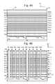
- a first group of NAND strings(Group 0 ) includes NAND strings NS 0 A, NS 0 B, NS 0 C and NS 0 D which are connected at bottom portions to a source line SL 0 and at top portions to a bit line BL 0 .
- a second group of NAND stringsare connected at bottom portions to a source line SL 1 and at top portions to a bit line BL 1
- a third group of NAND stringsare connected at bottom portions to a source line SL 2 and at top portions to a bit line BL 3
- a sixteenth group of NAND stringsare connected at bottom portions to a source line SL 15 and at top portions to a bit line BL 15
- the sixteenth groupincludes NAND strings NS 0 A- 15 , NS 0 B- 15 , NS 0 C- 15 and NS 0 D- 15 .
- the number of NAND strings and their arrangementis an example only.
- each source lineis connected at one end to the slit structure (STa) which is an example of a passageway in the stack.
- the slit structurecan be generally rectangular and extend crosswise to the source lines, in one approach.
- the slit structureextends in the x direction, orthogonal to the source lines, which extend in the y direction.
- the source linesextend like fingers of a comb.
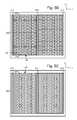
- FIG. 2Bdepicts an example set of NAND strings in the memory device of FIGS. 1A and 1B , where electrical contacts to source lines of the NAND strings are made via opposing slit structures.
- the slits STa and STbare opposing slits, with a plurality of memory holes/NAND strings between them.
- Each slitis connected to a plurality of source lines which are formed by metal in voids in a substrate, as discussed further below.
- the metal in each voidis connected to the bottom of a respective set of memory holes.
- the NAND strings and their memory holesare arranged in groups such as Group 0 and Group 15 .
- the source lines of a first groupe.g., SL 0
- the source lines of a second groupe.g., SL 15
- the odd-numbered groupsare connected to one slit structure
- the even-numbered groupsare connected to the other slit structure.
- Thiscan facilitate the layout of the source contacts.
- Further efficienciesare achieved by connecting several NAND strings and their memory holes to one source line.
- the number of memory holes which are connected to one source linemay be limited by factors such as the ability to etch and deposit films in an elongated horizontal void in a substrate. This example has four memory holes per source line.
- the source linesmay extend diagonally to the slits. It is also possible for a memory hole to connect to more than one slit structure.
- FIG. 3Adepicts an overview of a method for fabricating a memory device with a low resistance source contact.
- a first optioncan be used in which a void is formed in a substrate dielectric, and the void is connected to the bottom of the memory holes and the bottom of the passageway before a plurality of materials are deposited.
- the substrate dielectriccan be, e.g., a silicon substrate or a dielectric layer on a silicon substrate. It is possible to form the void in the silicon substrate, but it would be problematic to have the source line shorted to the substrate since during operation a bias can be applied to the source line. Providing the void in a dielectric layer insulates the void from the substrate.
- step 300includes forming memory holes and a passageway in a stack on a substrate.
- the memory holes and the passagewaycan be formed concurrently or separately.
- One or more memory holes and one or more passagewaysare formed.
- a passagewayextends generally vertically in the stack, from a bottom of the stack to a top of the stack.
- a passagewaycould in theory alternatively extend at an oblique angle to the plane of the substrate.
- Step 301includes forming a void in a substrate dielectric. This can involve introducing an etchant via the memory holes and passageway which removes a sacrificial material in the dielectric layer.
- Step 302involves depositing materials in the passageway, void and memory holes. Generally, each material is deposited as a continuous film throughout the passageway, void and memory hole.
- Step 303involves depositing metal in the passageway, but not in the memory holes.
- a voidis formed in a substrate dielectric, and the void is connected to the bottom of the memory holes before a plurality of materials are deposited.
- the passagewayis subsequently formed and connected to the void.
- An advantage of this approachis that the passageway can be used to provide a replacement material for the control gate layers before the passageway is connected to the void. Also, the deposition and removal of the dielectric material from the passageway is avoided, so that the amount of dielectric material and etchant is reduced. Doping of the channel material in the passageway is also avoided.
- step 304involves forming memory holes in the stack.
- Step 305involves forming a void in a substrate dielectric.
- Step 306involves depositing materials in the void and memory holes, but not in the passageway, which has not yet been created.
- Step 307involves forming the passageway from the top of the stack to the void. Step 303 is then performed, as discussed.
- FIG. 3Bdepicts an example implementation of the first option of the method of FIG. 3A .
- the process of FIG. 3Bis discussed also in connection with FIG. 4B to 4I .
- Step 310involves forming a trench in a substrate dielectric.
- the substratecan comprise silicon and the dielectric layer can comprise polysilicon, for example.
- One reason to provide the trench in a dielectric layeris that the substrate may receive a voltage which would interfere with the source contact.
- the trenchis formed in a desired pattern in which horizontal portions of the source contact will be located.
- the trenchmay include portions which are relatively wide or relatively deep. Example patterns are depicted in FIGS. 2A , 2 B and 5 A to 5 C.
- a trenchis meant to include, e.g., a region of the substrate which is removed in specified pattern, where the region is filled with a sacrificial material, and the sacrificial material is subsequently removed, forming a void.
- Step 311involves depositing a sacrificial material in the trench.
- the sacrificial materialcan be any material which can be selectively etched compared to the stack materials. For example, this can be a nitride such as silicon nitride (Si3N4), amorphous silicon, or polysilicon.
- Step 311 ainvolves covering the trench with additional dielectric material. The additional dielectric material insulates the voids from the stack but is not required.
- Step 312involves forming a stack of alternating control gate layers and dielectric layers over the trench, e.g., on the substrate dielectric.
- the stackcan be on the additional dielectric material ( 106 , FIG. 7H ) which covers the trench. See FIG. 4A .
- the stackmay be formed directly on the sacrificial material in the trench.
- the stackcovers the trench and the sacrificial material.
- the dielectric layers in the stackmay comprise oxide and/or nitride, for instance.
- the stackis initially formed with the final material for the control gate layers.
- the stack as initially formedincludes a sacrificial material which is replaced by a replacement material to provide the final material.
- a sacrificial material of the control gate layerscan be replaced with metal.
- Step 313involves etching memory holes and a passageway in the stack, down to the sacrificial material in the void, thereby exposing portions of the sacrificial material in the void.
- a slitis an example of a passageway in the stack.
- One or more passagewaysare formed.
- a masksuch as photoresist or a hard mask can be applied to the top of the stack, where openings in the mask define the etch pattern. For example, a dry etch can be used. The etching depth can be controlled so that it stops when the sacrificial material is reached.
- the passageway and memory holescan be etched at the same time or separately.
- the memory holesare typically circular in cross-section, but other shapes are possible as well.
- the passagewaycan be generally rectangular, although other shapes are possible as well.
- Step 314involves removing the sacrificial material in the substrate dielectric via the memory holes and/or the passageway, thereby creating a void in the trench.
- the sacrificial materialcan be etched away using an isotropic (non-directional) etch.
- An etchantcan be supplied to the sacrificial material via the passageway and/or memory holes. The void and the passageway together form a path from the bottom of the memory holes to the top of the stack.
- Step 315involves depositing a plurality of materials in the passageway, void and memory holes.
- the materialscan be deposited as films one material at a time in a prescribed sequence. For each material, this can involve, e.g., supplying the material at the top of the passageway and/or memory holes.
- the deposition of the materials as described hereincan involve chemical vapor deposition (CVD) and/or atomic layer deposition (ALD).
- the deposited materialcoats the inner surfaces or walls of the passageway, void and memory holes, forming a film.
- each filmcoats an inner surface of the passageway, void and the memory hole, to form a continuous annular film which extends from a top of the memory hole to the bottom of the memory hole, laterally through the void, and vertically through the passageway, to the top of the stack.
- the first deposited filmis in contact with the inner surfaces
- the second deposited filmis in contact with the first deposited film, and so forth.
- the plurality of materialsinclude a block oxide, followed by a nitride (e.g., Si3N4), followed by a tunnel oxide, in an oxide-nitride-oxide (O—N—O) configuration.
- the block oxide and tunnel oxidecan include, e.g., silicon oxide, silicon nitride, silicon oxynitride, or other high-k insulating materials.
- the block oxide and tunnel oxidecan be the same material or different materials.
- Nitrideis an example of a programmable film which can be altered to store data.
- nitrideis an example of a charge storage material or charge trapping material which can store no charge, or a specified amount of charge, which corresponds to a data state.
- control gate layersare metal and a channel layer is polysilicon, so that memory cells in a metal-oxide-nitride-oxide-silicon (MONOS) configuration are provided.
- control gate layersare doped polysilicon and the channel layer is polysilicon, so that memory cells in a silicon-oxide-nitride-oxide-silicon (SONOS) configuration are provided.
- MONOSmetal-oxide-nitride-oxide-silicon
- SONOSsilicon-oxide-nitride-oxide-silicon
- Step 316involves depositing a channel material in the passageway, void and the memory holes. For example, this can involve supplying polysilicon at the top of the passageway and memory holes.
- the polysilicon filmcan form a channel in the memory holes which provides a current path in a NAND string.
- the channel material which is proximate to the memory cells in the memory holesis undoped. Portions of the channel material above the SGD transistor and below the SGS transistor can be doped.
- the channel material in a memory holesis also referred to as the body of a NAND string.
- Step 317involves depositing a dielectric material (e.g., silicon oxide, SiO2) in the passageway, void and the memory holes. Due to the larger minimum cross-sectional dimension of the passageway and void compared to the memory holes, an air gap remains in the passageway and void after this deposition. That is, the passageway and void are not completely filled by the dielectric material.
- the minimum cross-sectional dimension of the passageway and voidis larger than the minimum cross-sectional dimension of the memory holes by some specified amount such as by at least 10-30%. The amount depends on the specifics of the geometry as well as the deposition process used. On the other hand, core regions of the memory holes may be completely filled by the dielectric material.
- Step 318involves covering the memory holes with a mask at the top of the stack.
- the maskhas openings for the passageways.
- Step 319involves removing the dielectric material from the passageway and void (but not from the memory holes) via the passageway, thereby exposing the channel material in the passageway and void.
- this removalcan involve a wet etch or a vapor etch.
- a wet etchinvolves supplying a liquid phase etchant at the top of the passageway.
- a vapor etchinvolves supplying a vapor phase etchant at the top of the passageway. This can be an isotropic etch which selectively removes the dielectric material.
- the passageway and voidmay become partly or fully filled by the dielectric material depending on their minimum cross-sectional dimension. In this case, removal of the dielectric material from the passageway and void is still possible but would be more difficult.
- Step 320involves doping the channel material in the passageway and void, via the passageway.
- thiscan involve gas phase doping in which a dopant is supplied at the top of the passageway.
- a dopant at a concentration of 10 ⁇ 20 to 10 ⁇ 21 cm-3 or morecan be used.
- An n-type dopant such as Arseniccan be used, for instance.
- a high doping concentrationis desirable to reduce the resistance of the channel material in the passageway and void.
- step 320 athere is an option to deposit additional doped polysilicon on the doped channel material, which itself may be doped polysilicon.
- additional doped polysiliconmay be more heavily doped than the doped channel material.
- the additional polysiliconmay be introduced via the passageway, and may or may not subsequently be removed from the passageway. This step thus involves introducing additional doped material to the void via the passageway, after the doping the portion of the channel material which is in the void.
- Step 321involves performing a heat treatment, e.g., anneal, for the memory device to cause the dopant to diffuse upward in the channel material in the memory holes, starting from a bottom of the memory holes.
- a heat treatmente.g., anneal
- the anneal time and temperaturewill determine the upward distance of the diffusion in the channel material. As a rough example, a temperature of 1000 degree C. for 10 seconds can be used.
- the anneal conditionsdepend on the specifics of the geometry, dimensions, and materials.
- the upward diffusion of the dopantcan be helpful is allowing the SGS transistors to generate gate-induced drain leakage (GIDL).
- GIDLgate-induced drain leakage
- a doped region of the channel materialcan provide a drain region of the SGS transistor.
- GIDLcauses holes to flow from the drain region of the SGS transistor into the channel layer to charge up the channel layer, such as in an erase operation.
- the heating time and duration, or thermal budgetcan be controlled to cause the dopant to diffuse upward in the channel material to a bottom control gate layer (e.g., the SGS layer) of the control gate layers. The diffusion can be approximately even with the bottom of the bottom control gate layer, for instance (see level L 1 a in FIG. 4F ).
- the additional ability to generate GIDL at the SGS transistoris advantageous since the SGD transistor can be optimized for minimum leakage rather than being used to generate GIDL.
- the order of the steps as shownis not necessarily required.
- the heat treatmentcan be performed after the metal is deposited.
- Step 322deposits a metal in the passageway and void, via the passageway, to form a conductive path from the bottom of each memory hole through the void to a top of the passageway.
- a metalfor example, Tungsten is a suitable metal.
- An adhesion layersuch as titanium nitride (TiN) may be deposited before the metal to help adhere the metal to the doped polysilicon channel material.
- TiNtitanium nitride
- the metal and the doped channel materialform a continuous conductive path from a bottom of the memory holes to a top of the passageway.
- Step 323performs additional processing to provide a source contact from the top of the metal in the slit to an upper metal layer.
- the materials in the memory holeare etched back slightly to a desired distance from the top surface of the top control gate layer, e.g., the SGDL layer ( FIG. 4H ).
- a cap materialis deposited in the recessed are at the top of the memory hole.
- a contact materialcan then be formed on the cap material by appropriate patterning of the contact material.
- FIG. 3Cdepicts an example implementation of the second option of the method of FIG. 3A .
- the process of FIG. 3Cis discussed also in connection with FIG. 7 A 1 to 7 K. Some of the steps are similar to those in FIG. 3B .
- Step 350involves forming a trench in a substrate dielectric.
- Step 351involves depositing a sacrificial material in the trench.
- Step 352involves covering the trench with additional dielectric material.
- Step 353 ainvolves forming initial layers of alternating control gate layers and dielectric layers of the stack over the trench, on the substrate dielectric.
- Step 353 binvolves etching an opening in the initial layers and depositing an etch stop material (e.g., polysilicon).
- an etch stop materiale.g., polysilicon
- Step 354involves forming remaining alternating control gate layer and dielectric layers of the stack over the initial layers. The etch stop material is thus provided on the substrate dielectric within the stack.
- Step 355involves etching memory holes in the stack, thereby exposing portions of the sacrificial material in the substrate dielectric. For example, a dry etch can be used.
- Step 356involves removing the sacrificial material in the trench via the memory holes, thereby creating a void in the trench.
- An etchant which is selective of the sacrificial materialcan be provided via the memory holes.
- Step 357involves depositing a plurality of materials in the void and memory holes. The materials are supplied at the top of the memory holes.
- Step 358involves depositing a channel material in the void and the memory holes. For example, this can involve supplying polysilicon at the top of the memory holes.
- Step 359involves depositing a dielectric material in the void and the memory holes, via the memory holes, leaving an air gap in the void.
- Step 360involves etching from the top of the stack to the etch stop material, thereby forming an opening in the stack from the top of the stack to the top of the etch stop material. A portion of the etch stop material may be consumed, leaving a remainder of the etch stop material.
- Step 361involves removing the remainder of the etch stop material via the opening, so that the opening extends down to the substrate dielectric. In one approach, this etching step does not pierce the materials in the void.
- Step 362involves providing a replacement material for the control gate layers via the opening. For example, the sacrificial material of the control gate layers can be removed by etching, creating voids between the dielectric layers of the stack, followed by introducing a metal (e.g., W) into the voids via the opening. At step 362 a , metal which remains in the opening is removed by cleaning to avoid shorting the control gate layers.
- Step 363involves depositing a liner (e.g., SiO2) in the opening which is thicker than a final target value.
- a linere.g., SiO2
- Step 364involves etching through the bottom of the liner, through part of the substrate dielectric and reaching the void, thereby piercing a hole through the materials in the void (e.g., the programmable material, channel material and dielectric material) and forming a passageway from the void to the top of the stack. The etching can pierce the top of the void only, or both the top and bottom of the void.
- Step 365includes covering the memory holes with a mask.
- Step 366involves removing the dielectric material from the void, via the opening, thereby exposing the channel material in the void. For example, an etchant can be introduced to the void from the top of the passageway. Steps 320 - 323 of FIG. 3B are then performed.
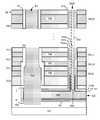
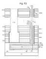
- FIG. 4Adepicts a cross-sectional view of a semiconductor device including a stack 410 formed on a dielectric layer 105 on a substrate 101 , consistent with step 312 of FIG. 3B .
- the substratecomprises trenches such as a trench 420 filled with a sacrificial material 421 , and a trench 430 filled with a sacrificial material 431 .
- the stack 410is fabricated on the dielectric layer 105 on the substrate.
- the stackincludes alternating control gate layers and dielectric layers.
- the control gate layerscan include word line layers (e.g., WLL 0 -WLL 7 ) which are used to provide control gate voltages for memory cells in the final memory device.
- a top control gate layer (e.g., SGDL) of the control gate layersis a control gate of a drain-side select gate transistor
- a bottom control gate layer (e.g., SGSL) of the control gate layersis a control gate of a source-side select gate transistor.
- Dielectric layers DL 0 -DL 10are also depicted. The number of layers shown is an example only. The stack can be fabricated by depositing each layer in turn upon the previous layer.
- control gate layerscomprise polysilicon which is doped during deposition, and these layers remain in the final memory device.
- control gate layersare treated to convert them to metal silicide.
- a sacrificial materialis initially provided in the control gate layers and this material is replaced with a highly conductive material such as metal in the final memory device.
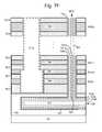
- FIG. 4Bdepicts the semiconductor device of FIG. 4A after steps 313 and 314 of FIG. 3B .
- Memory holes MH 0 -MH 7 and slits ST 1 and ST 2are etched vertically through the stack, from a top (TP) of the stack at the level L 2 , to the sacrificial material at the bottom of the stack, denoted by level L 1 .
- the voids 422 and 432are created.
- the slit ST 1 and the void 422form a path P 1
- the slit ST 2 and the void 432form a path P 2 .
- a region 435is depicted in further detail in FIG. 4C .
- a level L 1 ais at the bottom of the SGSL layer.
- more than one SGS or SGD layeris provided in a stack.
- two SGD layersmay be provided, separated by a dielectric layer. That is, multiple control gate layers can be used to form a select device.
- a layercomprises multiple sublayers of different materials.
- the memory hole and slitsare shown as having a uniform cross-section through the height of the stack, in the z direction, for simplicity.
- the cross-sectioncan vary due to the etching process.
- the cross-sectionis tapered, becoming narrower at the bottom of the stack.
- FIG. 4Cdepicts a close up view of the region 435 of FIG. 4B .
- Dashed linesrepresent the area of the slit ST 1 , the memory hole MH 0 and the void 422 , which have respective cross-sectional dimensions of Aslit, Amh and Avoid.
- the slit and voidtogether form the path P 1 .
- the dimensions Aslit and Avoidare greater than Amh. Aslit is shown as being greater than Avoid, but this is an example only.
- the slit and memory holeare generally vertically extending while the void is generally horizontally extending. A portion of the substrate 101 is also depicted.
- FIG. 4Ddepicts the semiconductor device of FIG. 4C after steps 315 - 317 of FIG. 3B .
- the plurality of materialsinclude an oxide-nitride-oxide (ONO) set of films 440 comprising a block oxide 452 , a charge trapping film 451 (a programmable film) and a tunnel oxide 450 .
- the plurality of materialsalso include a channel material such as polysilicon, and a dielectric material such as oxide.
- Portions 440 a , 440 b and 440 c of the ONO filmsare in the memory hole, void and slit, respectively.
- Portions 441 a , 441 b and 441 c of the channel materialare in the memory hole, void and slit, respectively.
- Portions 442 a , 442 b and 442 c of the dielectric materialare in the memory hole, void and slit, respectively.
- the materialscoat the inner surfaces of the passageway and memory holes, including a wall or inner surface 460 of the slit, a wall or inner surface 464 of the void and a wall or inner surface 462 of the memory hole. Since the cross-sectional dimension of the slit and void is greater than that of the memory hole, the memory hole becomes filled by the dielectric material while an air gap remains in the slit and void.
- the slithas a gap 470 and the void has a gap 471 .
- a dashed line 463represents the portion of the dielectric material that fills the memory hole MH 0 .
- Each filmcoats an inner surface of the passageway and the memory hole, to form a continuous annular film which extends from a top 416 of the memory hole to the bottom 485 of the memory hole and through the passageway P 1 back to the top of the slit 415 or passageway P 1 .
- FIG. 4Edepicts the semiconductor device of FIG. 4D after steps 318 and 319 of FIG. 3B .
- a mask Msuch as photoresist at the top of the stack covers the memory hole and has an opening for the slit ST 1 .
- An etchantis supplied to the passageway via the top of the slit to remove the dielectric material in the passageway.
- the dielectric material 442 aremains in the memory hole. The mask prevents the etchant from entering the memory hole.
- FIG. 4Fdepicts the semiconductor device of FIG. 4E after steps 320 and 321 of FIG. 3B .
- the channel materialis doped to provide a doped channel material 441 bd and 441 cd .
- a heat treatmentcause a portion 441 ad of the channel material in the memory hole to be doped as well, between roughly a level L 1 , at the bottom of the memory hole or stack and up to a level L 1 a at the bottom of the SGSL layer or higher, such as to a level L 1 b .
- the maskprevents the dopant from entering the top of the memory hole.
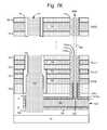
- FIG. 4Gdepicts the semiconductor device of FIG. 4F after step 322 of FIG. 3B .
- a metalsuch as tungsten is added which fills the passageway P 1 .
- One portion 480 of the metalis in the slit and another portion 481 is in the void 422 .
- the maskprevents the metal from entering the memory hole.
- the metal in the voidextends to a bottom of each memory hole of a plurality of memory holes, such as the bottom 485 of MH 0 .
- the metalcan be provided concurrently in a plurality of voids in the substrate dielectric, such as metal portions 481 and 482 in FIG. 5A .
- the metal in each voidconnects to the portion 480 of the metal in a slit and to a bottom 485 of each memory hole of a group of memory holes.
- a metal conductive pathis formed from the bottom of each memory hole to the top (TP) of the stack.
- FIG. 4Hdepicts the semiconductor device of FIG. 4G after step 323 of FIG. 3B .
- Additional processingcan include connecting the top of the slit structure to a source line voltage and connecting the top of the memory hole to a bit line voltage.
- the materials in the memory holemay be etched back slightly to make room to deposit a cap material 494 .
- contact structures 461 and 492can be provided above the slit and memory hole which extend upward to a metal layer.
- a NAND string 499is formed in the memory hole.
- the NAND stringincludes a SGD transistor 490 , example memory cells 491 and 492 and an SGS transistor 493 .
- FIG. 4Idepicts a cross-sectional view of the memory hole of FIG. 4H along the line 495 .
- Each of the memory holesis filled with a plurality of annular layers or films, and a core region of each of the memory holes is filled with a core filler material.
- the annular layersare annular cylinders.
- the layersinclude a block oxide 452 , a charge trapping film 451 , a tunnel oxide 450 and the portion 441 a of the channel material.
- the dielectric material 442 ais also depicted.
- the charge trapping filmis between the block oxide and the tunnel oxide.
- FIG. 5Adepicts a cross-sectional view along the level L 1 of the memory device of FIG. 4B , showing a first example pattern formed by a source contact material in passageways and voids.
- the source contactincludes the portion 480 in the slit ST 1 and the portion 481 in the void 422 . Additional portions of the source contacts which are in additional voids in the substrate dielectric, such as a portion 482 are also depicted.
- the slit ST 2is connected to a metal portion on both sides of the slit.
- the cross-sectional view of FIG. 4Bis coincident with the line 500 .
- the metalis provided in opposing slits (e.g., ST 1 and ST 2 ) in the stack.
- a plurality of memory holese.g., MH 0
- the metal in each slitconnects to metal (e.g., metal portions 481 , 482 ) in a respective void in the substrate dielectric.
- the metal in the voids in the substrate dielectriccomprise spaced apart parallel regions which extend, at one end, from a bottom of a respective slit.
- the metal in each voidconnects to a bottom of each memory hole of a respective group of memory holes.
- the metal portion 481connects to the bottom of each of memory holes MH 0 -MH 3 and the metal portion 482 connects to the bottom of each of memory holes MH 8 -MH 11 .
- Support postscan optionally be provided to provide support for the layers in the stack.
- the support postare represented by squares to distinguish them from the memory holes in the figures, but can have a circular cross-section.
- the support postsextend through the stack and can be interspersed among the memory holes in a periodic pattern.
- additional slitscan be provided and used to replace a sacrificial material in the control gate layers.
- the additional slitscan be formed, and an etchant provided in the additional slits which removes the sacrificial material.
- a replacement materialcan then be provided via the additional slits.
- the additional slitsare subsequently filled with insulation.
- the fabrication of the additional slitscan be independent of the fabrication of the slits used for the source contacts.
- the sacrificial material in the control gate layersis replaced after the films are deposited in the memory holes. In other cases, the additional slits are not provided.
- the slits used to form the source contactscan also be used to provide the replacement material for the control gate layers.
- FIG. 5Bdepicts a second example pattern formed by the source contact material, as an alternative to FIG. 5A .
- the metal in the void in the substrate dielectriccomprises a mesh or grid GR of conductive lines which extend in the x and y directions.
- a line 520extends in the x direction and a line 521 extends in the y direction.
- Support posts(such as example support post SP 2 ), represented by squares, can optionally be provided, as discussed.
- FIG. 5Cdepicts a third example pattern formed by the source contact material, as an alternative to FIG. 5A .
- a substantially continuous region CRis provided between the slits.
- a larger metal regionis desirable since the resistance is reduced in proportion to the volume of the metal region.
- Support posts(such as example support post SP 3 ), represented by squares, can optionally be provided, as discussed.
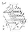
- FIG. 6Adepicts an alternative semiconductor device in which a plurality of layers including a programmable film are formed at the bottom of a memory hole.
- the deviceprovides an alternative to the configuration of FIG. 4C .
- a doped channel region 620is formed in a substrate 601 .
- the stackis deposited and a slit ST 1 a and a memory hole MH 0 a are etched in the stack, down to the doped channel region 620 .
- a mask 660is then provided over the slit to prevent memory films from entering the slit. Instead, the memory films 610 are deposited along the sidewalls and bottom of the memory hole.
- a memory film region 611is at the bottom of the memory hole.
- An etchantis introduced into the memory hole to etch away the memory film region 611 at the bottom of the memory hole, and thereby expose a portion of the doped channel region.
- a small region at the top of the doped channel regionmay be etched away as well.
- FIG. 6Bdepicts the alternative semiconductor device of FIG. 6A in which the layers are etched through to form an opening at the bottom of the memory hole.
- the channel material 622is deposited along the side of the memory film 610 .
- a portion 621 of the channel material 622enters the etched away region at the top of the doped channel region, to form a contact to the doped channel region.
- the dielectric material 630is provided in the memory hole.
- the mask over the slitis removed and a mask, not shown, is placed over the memory hole, after which metal 640 is deposited in the slit to form a conductive vertical path to the doped channel region 620 .
- the combination of the metal 640 and the doped channel regionforms a conductive source contact to the bottom of the memory hole.
- a thin film transistor (TFT), not shown,can also be provided in the channel.
- FIG. 7 A 1depicts a semiconductor device after step 353 b of FIG. 3C .
- the sacrificial material 701is formed in the dielectric layer 105 on the substrate.
- One or more initial layers of the stackare then deposited, such as DL 0 , DL 1 , SGSL and WLL 0 .
- the number of initial layerscorresponds to the desired height of the etch stop material.
- a portion of the stackis etched, creating an opening, and the etch stop material 710 is deposited in the opening.
- the etch stop materialmay be roughly twice as wide as a memory hole.
- FIG. 7 A 2depicts the semiconductor device of FIG. 7 A 1 after step 354 of FIG. 3C .
- the semiconductor deviceis similar to that of FIG. 4B except the passageways have not yet been formed. Additionally, the etch stop material 710 is provided on the dielectric layer 105 , within the stack. A region 735 is depicted in further detail in FIG. 7B .
- FIG. 7Bdepicts the semiconductor device of FIG. 7 A 2 after steps 355 to 359 of FIG. 3C .
- the plurality of materialsinclude an oxide-nitride-oxide set of films, a channel material and a dielectric material.
- Portions 740 a and 740 b of the ONO filmsare in the memory hole MH 0 and void 722 , respectively.
- Portions 741 a and 741 b of the channel materialare in the memory hole and void, respectively.
- Portions 742 a and 742 b of the dielectric materialare in the memory hole and void, respectively.
- the materialscoat the inner surfaces of the void 722 and memory holes, including a wall or inner surface 761 of the void and a wall or inner surface 762 of the memory hole. Since the cross-sectional dimension of the void is greater than that of the memory hole, the memory hole becomes filled by the dielectric material while an air gap 771 remains in the void.
- a dashed line 763represents the portion of the dielectric material that fills the memory hole MH 0 .
- Each filmcoats an inner surface of the void and the memory hole, to form a continuous annular film which extends from a top 716 of the memory hole to the bottom 785 of the memory hole and through the void.
- FIG. 7Cdepicts the semiconductor device of FIG. 7B after step 360 of FIG. 3C .
- An etching processsuch as reactive on etching involves etching through a portion of the stack until the etch stop material 710 is reached. This results in an opening 711 in the stack.
- the etching depthcan be easily controlled.
- the etch stop materialmay be wider than the opening to provide a margin for error which prevents the opening from bypassing the etch stop material.
- FIG. 7Ddepicts the semiconductor device of FIG. 7C after step 361 of FIG. 3C .
- the remaining etch stop materialis removed so that the opening 711 a extends down to the dielectric layer 105 on the substrate 101 .
- the etch stop materialis a sacrificial material. By removing the etch stop material, an opening which extends to the dielectric layer 105 can be easily formed. In contrast, etching through the stack directly and stopping at the dielectric layer 105 would be more difficult. At this point, the layers in the stack are readily accessible via the opening 711 a for replacing the material of the control gate layers before accessing the void.
- FIG. 7Edepicts the semiconductor device of FIG. 7D after removing a sacrificial material of the control gate layers, consistent with step 362 of FIG. 3C .
- an etchantcan be supplied to the opening 711 which etches away the material of the SGSL, WLL 0 , WLL 1 , . . . , SGDL layers, resulting in voids between the dielectric layers DL 0 -DL 10 of the stack, such as example voids 770 - 773 .
- FIG. 7Fdepicts the semiconductor device of FIG. 7E after providing a replacement material for the control gate layers, consistent with step 362 of FIG. 3C .
- a metalsuch as W can be deposited in the voids 770 - 773 via the opening 711 to provide the replacement material 795 - 798 (shown by a slanted line pattern) for the control gate layers.
- FIG. 7Gdepicts the semiconductor device of FIG. 7F after step 363 of FIG. 3C .
- a liner 780 having a bottom 781is deposited in the opening.
- FIG. 7Hdepicts the semiconductor device of FIG. 7G after step 364 of FIG. 3C .
- the etching processremoves a region 799 .
- a passageway PYis formed by the opening 711 in the stack and the region 798 .
- the etchingproceeds through the bottom of the liner, a the additional dielectric material 106 of the dielectric layer 105 which is above the void 722 , the plurality of materials 740 b , 741 b and 742 b at a top (T) of the void and optionally, the plurality of materials at a bottom (B) of the void.
- Piercing the top of the voidis sufficient to form the passageway from the top of the stack to the void.
- Piercing the bottom of the voidadditionally is also acceptable. This allows a wider margin of error in the etching depth.
- the etchingterminates before the substrate 101 is reached.
- the void 722is shown as having a similar width or depth as the opening 711 in the figure for clarity.
- the opening 711can be relatively narrower than the void so that the portion of the stack which is consumed by the opening is minimized.
- a larger voidis desirable since it allows more metal to be deposited, resulting in a lower resistance.
- FIG. 7Idepicts the semiconductor device of FIG. 7H after step 366 of FIG. 3C .
- the dielectric material 742 b in the void 722is removed by supplying an etchant via the passageway PY.
- the etchantmay also remove some of the liner 780 , resulting in a recessed liner 781 .
- FIG. 7Jdepicts the semiconductor device of FIG. 7I after steps 320 and 321 of FIG. 3B .
- the channel material 741 b ( FIG. 7I ) in the voidis doped to provide a doped channel material 741 bd .
- FIG. 7Kdepicts the semiconductor device of FIG. 7J after step 322 of FIG. 3B .
- Metalis deposited in the void and passageway, including a metal portion 790 in the void and a metal portion 791 in the passageway, forming a metal conductive path from the bottom 785 of the memory hole to the top (TP) of the stack. This is the contact to the source end of the memory hole.
- one embodimentprovides a method for fabricating a 3d stacked non-volatile memory device.
- the methodincludes: forming a memory hole in a stack, the stack comprising alternating control gate layers and dielectric layers on a substrate dielectric; forming a void in the substrate dielectric, a bottom of the memory hole is connected to the void; forming a passageway in the stack between a top of the stack and the void; depositing a plurality of materials in the void and the memory hole, the plurality of materials comprise a programmable material, a channel material and a dielectric material; removing a portion of the dielectric material which is in the void, exposing a portion of the channel material which is in the void; doping the portion of the channel material which is in the void, the doping comprises introducing a dopant to the void via the passageway; and depositing a metal in the void and the passageway, the metal extends to the bottom of the memory hole.
- a method for fabricating a 3d stacked non-volatile memory deviceincludes: forming a memory hole in a stack, the stack comprising alternating control gate layers and dielectric layers on a substrate dielectric; forming a passageway in the stack; forming a void in the substrate dielectric by etching away a sacrificial material in the substrate dielectric using an etchant introduced via at least one of the passageway or the memory hole, the void connects a bottom of the passageway to a bottom of the memory hole; depositing a plurality of materials in the passageway, the void and the memory hole, the plurality of materials comprise a programmable material, a channel material and a dielectric material; removing a portion of the dielectric material which is in the void, exposing a portion of the channel material which is in the void, the removing comprises introducing an etchant into the void via the passageway; doping the portion of the channel material which is in the void, the doping comprises introducing
- a method for fabricating a 3d stacked non-volatile memory deviceincludes: forming a memory hole in a stack, the stack comprising alternating control gate layers and dielectric layers on a substrate dielectric; forming a void in the substrate dielectric by etching away a sacrificial material in the substrate dielectric using an etchant introduced via the memory hole; depositing a plurality of materials in the void and the memory hole, the plurality of materials comprise a programmable material, a channel material and a dielectric material; forming a passageway in the stack which extends from a top of the stack to the void; removing a portion of the dielectric material which is in the void, exposing a portion of the channel material which is in the void, the removing comprises introducing an etchant into the void via the passageway; doping the portion of the channel material which is in the void, the doping comprises introducing a dopant to the void via the passageway; and depositing a
Landscapes
- Engineering & Computer Science (AREA)
- Computer Hardware Design (AREA)
- Physics & Mathematics (AREA)
- Condensed Matter Physics & Semiconductors (AREA)
- General Physics & Mathematics (AREA)
- Manufacturing & Machinery (AREA)
- Microelectronics & Electronic Packaging (AREA)
- Power Engineering (AREA)
- Chemical & Material Sciences (AREA)
- General Chemical & Material Sciences (AREA)
- Inorganic Chemistry (AREA)
- Chemical Kinetics & Catalysis (AREA)
- Semiconductor Memories (AREA)
- Non-Volatile Memory (AREA)
Abstract
Description
- The present technology relates to techniques for fabricating a 3D non-volatile memory device.
- Recently, ultra high density storage devices have been proposed using a 3D stacked memory structure. One example is referred to as a Bit Cost Scalable (BiCS) architecture. For example, a 3D NAND stacked memory device can be formed from an array of alternating conductive and dielectric layers. A memory hole is etched in the layers to define many memory layers simultaneously. A NAND string is then formed by filling the memory hole with appropriate materials. A straight NAND string extends in one memory hole, while a pipe- or U-shaped NAND string (P-BiCS) includes a pair of vertical columns of memory cells which extend in two memory holes and which are joined by a bottom back gate. Control gates of the memory cells are provided by the conductive layers. However, various challenges are presented in fabricating such memory devices.
- Like-numbered elements refer to common components in the different figures.
FIG. 1A is a perspective view of a 3D stacked non-volatile memory device.FIG. 1B is a functional block diagram of the 3D stackednon-volatile memory device 100 ofFIG. 1A .FIG. 2A depicts an example set of NAND strings in the memory device ofFIGS. 1A and 1B , where electrical contacts to source lines of the NAND strings are made via a slit structure.FIG. 2B depicts an example set of NAND strings in the memory device ofFIGS. 1A and 1B , where electrical contacts to source lines of the NAND strings are made via opposing slit structures.FIG. 3A depicts an overview of a method for fabricating a memory device with a low resistance source contact.FIG. 3B depicts an example implementation of the first option of the method ofFIG. 3A .FIG. 3C depicts an example implementation of the second option of the method ofFIG. 3A .FIG. 4A depicts a cross-sectional view of a semiconductor device including a stack formed on a substrate, consistent withstep 312 ofFIG. 3B .FIG. 4B depicts the semiconductor device ofFIG. 4A aftersteps FIG. 3B .FIG. 4C depicts a close up view of theregion 435 ofFIG. 4B .FIG. 4D depicts the semiconductor device ofFIG. 4C after steps315-317 ofFIG. 3B .FIG. 4E depicts the semiconductor device ofFIG. 4D aftersteps FIG. 3B .FIG. 4F depicts the semiconductor device ofFIG. 4E aftersteps 320 and321 ofFIG. 3B .FIG. 4G depicts the semiconductor device ofFIG. 4F afterstep 322 ofFIG. 3B .FIG. 4H depicts the semiconductor device ofFIG. 4G afterstep 323 ofFIG. 3B .FIG. 4I depicts a cross-sectional view of the memory hole ofFIG. 4H along theline 495.FIG. 5A depicts a cross-sectional view along the level L1 of the memory device ofFIG. 4B , showing a first example pattern formed by a source contact material in passageways and voids.FIG. 5B depicts a second example pattern formed by the source contact material, as an alternative toFIG. 5A .FIG. 5C depicts a third example pattern formed by the source contact material, as an alternative toFIG. 5A .FIG. 6A depicts an alternative semiconductor device in which a plurality of layers including a programmable film are formed at the bottom of a memory hole.FIG. 6B depicts the alternative semiconductor device ofFIG. 6A in which the layers are etched through to form an opening at the bottom of the memory hole.- FIG.7A1 depicts a semiconductor device after
step 353bofFIG. 3C . - FIG.7A2 depicts the semiconductor device of FIG.7A1 after step354 of
FIG. 3C . FIG. 7B depicts the semiconductor device of FIG.7A2 after steps355 to359 ofFIG. 3C .FIG. 7C depicts the semiconductor device ofFIG. 7B afterstep 360 ofFIG. 3C .FIG. 7D depicts the semiconductor device ofFIG. 7C afterstep 361 ofFIG. 3C .FIG. 7E depicts the semiconductor device ofFIG. 7D after removing a sacrificial material of the control gate layers, consistent withstep 362 ofFIG. 3C .FIG. 7F depicts the semiconductor device ofFIG. 7E after providing a replacement material for the control gate layers, consistent withstep 362 ofFIG. 3C .FIG. 7G depicts the semiconductor device ofFIG. 7F afterstep 363 ofFIG. 3C .FIG. 7H depicts the semiconductor device ofFIG. 7G afterstep 364 ofFIG. 3C .FIG. 7I depicts the semiconductor device ofFIG. 7H afterstep 366 ofFIG. 3C .FIG. 7J depicts the semiconductor device ofFIG. 7I aftersteps 320 and321 ofFIG. 3B .FIG. 7K depicts the semiconductor device ofFIG. 7J afterstep 322 ofFIG. 3B .- Fabrication processes are provided for a 3D stacked non-volatile memory device which provide a source contact to memory holes. The source contact extends from the bottom of the memory holes to the top of a stack. A corresponding 3D stacked non-volatile memory device is also provided.
- Typically, the stack includes alternating control gate layers and dielectric layers. Memory films are provided in memory holes in the stack. For example, a film stack of oxide-nitride-oxide and a channel layer of polysilicon can be deposited along the sidewall of each memory hole. In one approach, two adjacent memory holes are joined together at the bottom and form a U-shaped NAND string, e.g., in the case of P-BiCS. In another approach, each memory hole forms a straight NAND string. In this case, challenges are presented in forming a contact to the bottom of the memory hole. One solution is to etch an opening in the bottom of the memory hole after depositing the memory films. Subsequently a channel/body material is deposited along with a dielectric material filler. The channel material extends through the opening at the bottom of the memory hole to a channel region of a substrate. Additionally, a vertical contact extends from the top of the stack to the channel region. However, such etching is difficult due to the high aspect ratio of the memory hole and can cause damage to the memory films along the sidewalls. Moreover, the channel region of the substrate has a relatively high resistance.
- Techniques provided herein avoid the need to etch through films at the bottom of a memory hole. Instead, a path is formed from the bottom of the memory hole to the top of the stack, and the memory films, channel material and dielectric material are deposited throughout the interior surfaces of the path and the one or more memory holes. The path can include a void in a substrate dielectric and a generally vertical passageway between the void and a top of the stack. Several memory holes can be joined to one passageway to allow concurrent deposition of the materials in the memory holes. Further, the dielectric material can be removed from the passageway and void, exposing the channel material and allowing the channel material to be doped to reduce its resistance. A heat treatment can be performed to cause the dopant to diffuse in the channel material upward in the memory holes. This configures the SGS transistor to generate gate-induced drain leakage (GIDL), such as for use in an erase operation.
- Finally, a metal is deposited in the passageway and void to provide a continuous, low resistance conductive path in the passageway and void. The resistance is much lower than for a thin film transistor (TFT) connection, for example. This provides better device performance and the potential to connect more memory holes to the same slit. Moreover, compared to a U-shaped NAND string, there is no need for a back gate. Also, a reduction in string current which is caused by the increased length of the U-shaped NAND string is avoided.
- The following discussion provides details of the construction of a memory device and of related techniques which address the above and other issues.
FIG. 1A is a perspective view of a 3D stacked non-volatile memory device. Thememory device 100 includes asubstrate 101. On the substrate are example blocks BLK0 and BLK1 of memory cells and aperipheral area 104 with circuitry for use by the blocks. Thesubstrate 101 can also carry circuitry under the blocks, along with one or more lower metal layers which are patterned in conductive paths to carry signals of the circuitry. The blocks are formed in anintermediate region 102 of the memory device. In anupper region 103 of the memory device, one or more upper metal layers are patterned in conductive paths to carry signals of the circuitry. Each block comprises a stacked area of memory cells, where alternating levels of the stack represent word lines. In one possible approach, each block has opposing tiered sides from which vertical contacts extend upward to an upper metal layer to form connections to conductive paths. While two blocks are depicted as an example, additional blocks can be used, extending in the x- and/or y-directions.- In one possible approach, the length of the plane, in the x-direction, represents a direction in which signal paths to word lines extend in the one or more upper metal layers (a word line or SGD line direction), and the width of the plane, in the y-direction, represents a direction in which signal paths to bit lines extend in the one or more upper metal layers (a bit line direction). The z-direction represents a height of the memory device.
FIG. 1B is a functional block diagram of the 3D stackednon-volatile memory device 100 ofFIG. 1A . Thememory device 100 may include one or more memory die108. The memory die108 includes amemory array 126 of memory cells,control circuitry 110, and read/write circuits 128. In a 3D configuration, the memory array can include the blocks BLK0 and BLK1 ofFIG. 1A . In a 2D configuration, the memory array can include the block BLK0 ofFIG. 5A . Thememory array 126 is addressable by word lines via arow decoder 124 and by bit lines via acolumn decoder 132. The read/write circuits 128 include multiple sense blocks130 (sensing circuitry) and allow a page of memory cells to be read or programmed in parallel. Typically acontroller 122 is included in the same memory device100 (e.g., a removable storage card) as the one or more memory die108. Commands and data are transferred between the host andcontroller 122 vialines 120 and between the controller and the one or more memory die108 vialines 118.- The
control circuitry 110 cooperates with the read/write circuits 128 to perform memory operations on thememory array 126, and includes astate machine 112, an on-chip address decoder 114, and apower control module 116. Thestate machine 112 provides chip-level control of memory operations. The on-chip address decoder 114 provides an address interface between that used by the host or a memory controller to the hardware address used by thedecoders power control module 116 controls the power and voltages supplied to the word lines and bit lines during memory operations. It can includes drivers for word lines in a 2D configuration, word line layers (WLLs) in a 3D configuration, SGS and SGD transistors and source lines. The sense blocks130 can include bit line drivers, in one approach. - In some implementations, some of the components can be combined. In various designs, one or more of the components (alone or in combination), other than
memory array 126, can be thought of as at least one control circuit. For example, a control circuit may include any one of, or a combination of,control circuitry 110,state machine 112,decoders 114/132,power control module 116, sense blocks130, read/writecircuits 128, andcontroller 122, and so forth. - Other types of non-volatile memory in addition to NAND flash memory can also be used.
FIG. 2A depicts an example set of NAND strings in the memory device ofFIGS. 1A and 1B , where electrical contacts to source lines of the NAND strings are made via a slit structure. In this example, each NAND string is straight, includes a drain-side select gate (SGD) transistor at the top, a source-side select gate (SGS) transistor at the bottom, and a number of memory cells in between. A first group of NAND strings (Group0) includes NAND strings NS0A, NS0B, NS0C and NS0D which are connected at bottom portions to a source line SL0 and at top portions to a bit line BL0. Similarly, a second group of NAND strings are connected at bottom portions to a source line SL1 and at top portions to a bit line BL1, a third group of NAND strings are connected at bottom portions to a source line SL2 and at top portions to a bit line BL3, . . . , and a sixteenth group of NAND strings are connected at bottom portions to a source line SL15 and at top portions to a bit line BL15. The sixteenth group includes NAND strings NS0A-15, NS0B-15, NS0C-15 and NS0D-15. The number of NAND strings and their arrangement is an example only.- In this example, each source line is connected at one end to the slit structure (STa) which is an example of a passageway in the stack. The slit structure can be generally rectangular and extend crosswise to the source lines, in one approach. The slit structure extends in the x direction, orthogonal to the source lines, which extend in the y direction. The source lines extend like fingers of a comb.
FIG. 2B depicts an example set of NAND strings in the memory device ofFIGS. 1A and 1B , where electrical contacts to source lines of the NAND strings are made via opposing slit structures. The slits STa and STb are opposing slits, with a plurality of memory holes/NAND strings between them. Each slit is connected to a plurality of source lines which are formed by metal in voids in a substrate, as discussed further below. The metal in each void is connected to the bottom of a respective set of memory holes.- The NAND strings and their memory holes are arranged in groups such as Group0 and Group15. The source lines of a first group (e.g., SL0) are connected to one of the slit structures (e.g., STa), and the source lines of a second group (e.g., SL15) are connected to the other of the slit structures (e.g., STb). In this manner, the odd-numbered groups are connected to one slit structure and the even-numbered groups are connected to the other slit structure. This can facilitate the layout of the source contacts. Further efficiencies are achieved by connecting several NAND strings and their memory holes to one source line. The number of memory holes which are connected to one source line may be limited by factors such as the ability to etch and deposit films in an elongated horizontal void in a substrate. This example has four memory holes per source line.
- Various other layouts may be used. For example, the source lines may extend diagonally to the slits. It is also possible for a memory hole to connect to more than one slit structure.
FIG. 3A depicts an overview of a method for fabricating a memory device with a low resistance source contact. A first option can be used in which a void is formed in a substrate dielectric, and the void is connected to the bottom of the memory holes and the bottom of the passageway before a plurality of materials are deposited. The substrate dielectric can be, e.g., a silicon substrate or a dielectric layer on a silicon substrate. It is possible to form the void in the silicon substrate, but it would be problematic to have the source line shorted to the substrate since during operation a bias can be applied to the source line. Providing the void in a dielectric layer insulates the void from the substrate.- An advantage of this approach is that the memory holes and passageway can be etched concurrently. In this option,
step 300 includes forming memory holes and a passageway in a stack on a substrate. The memory holes and the passageway can be formed concurrently or separately. One or more memory holes and one or more passageways are formed. A passageway extends generally vertically in the stack, from a bottom of the stack to a top of the stack. A passageway could in theory alternatively extend at an oblique angle to the plane of the substrate. Step301 includes forming a void in a substrate dielectric. This can involve introducing an etchant via the memory holes and passageway which removes a sacrificial material in the dielectric layer. Step302 involves depositing materials in the passageway, void and memory holes. Generally, each material is deposited as a continuous film throughout the passageway, void and memory hole. Step303 involves depositing metal in the passageway, but not in the memory holes. - In a second option, a void is formed in a substrate dielectric, and the void is connected to the bottom of the memory holes before a plurality of materials are deposited. The passageway is subsequently formed and connected to the void. An advantage of this approach is that the passageway can be used to provide a replacement material for the control gate layers before the passageway is connected to the void. Also, the deposition and removal of the dielectric material from the passageway is avoided, so that the amount of dielectric material and etchant is reduced. Doping of the channel material in the passageway is also avoided. In this option,
step 304 involves forming memory holes in the stack. Step305 involves forming a void in a substrate dielectric. This can involve introducing an etchant via the memory holes which removes a sacrificial material in the dielectric layer. Step306 involves depositing materials in the void and memory holes, but not in the passageway, which has not yet been created. Step307 involves forming the passageway from the top of the stack to the void. Step303 is then performed, as discussed. FIG. 3B depicts an example implementation of the first option of the method ofFIG. 3A . The process ofFIG. 3B is discussed also in connection withFIG. 4B to 4I . Step310 involves forming a trench in a substrate dielectric. The substrate can comprise silicon and the dielectric layer can comprise polysilicon, for example. One reason to provide the trench in a dielectric layer is that the substrate may receive a voltage which would interfere with the source contact. The trench is formed in a desired pattern in which horizontal portions of the source contact will be located. The trench may include portions which are relatively wide or relatively deep. Example patterns are depicted inFIGS. 2A ,2B and5A to5C. A trench is meant to include, e.g., a region of the substrate which is removed in specified pattern, where the region is filled with a sacrificial material, and the sacrificial material is subsequently removed, forming a void. Step311 involves depositing a sacrificial material in the trench. The sacrificial material can be any material which can be selectively etched compared to the stack materials. For example, this can be a nitride such as silicon nitride (Si3N4), amorphous silicon, or polysilicon. Step311ainvolves covering the trench with additional dielectric material. The additional dielectric material insulates the voids from the stack but is not required.- Step312 involves forming a stack of alternating control gate layers and dielectric layers over the trench, e.g., on the substrate dielectric. The stack can be on the additional dielectric material (106,
FIG. 7H ) which covers the trench. SeeFIG. 4A . Or, the stack may be formed directly on the sacrificial material in the trench. The stack covers the trench and the sacrificial material. The dielectric layers in the stack may comprise oxide and/or nitride, for instance. In one approach, the stack is initially formed with the final material for the control gate layers. In another approach, the stack as initially formed includes a sacrificial material which is replaced by a replacement material to provide the final material. For example, a sacrificial material of the control gate layers can be replaced with metal. - Step313 involves etching memory holes and a passageway in the stack, down to the sacrificial material in the void, thereby exposing portions of the sacrificial material in the void. A slit is an example of a passageway in the stack. One or more passageways are formed. A mask such as photoresist or a hard mask can be applied to the top of the stack, where openings in the mask define the etch pattern. For example, a dry etch can be used. The etching depth can be controlled so that it stops when the sacrificial material is reached. Generally, the passageway and memory holes can be etched at the same time or separately. The memory holes are typically circular in cross-section, but other shapes are possible as well. Moreover, the passageway can be generally rectangular, although other shapes are possible as well.
- The mask can then be removed. Step314 involves removing the sacrificial material in the substrate dielectric via the memory holes and/or the passageway, thereby creating a void in the trench. For example, the sacrificial material can be etched away using an isotropic (non-directional) etch. An etchant can be supplied to the sacrificial material via the passageway and/or memory holes. The void and the passageway together form a path from the bottom of the memory holes to the top of the stack.
- Step315 involves depositing a plurality of materials in the passageway, void and memory holes. The materials can be deposited as films one material at a time in a prescribed sequence. For each material, this can involve, e.g., supplying the material at the top of the passageway and/or memory holes. Generally, the deposition of the materials as described herein can involve chemical vapor deposition (CVD) and/or atomic layer deposition (ALD).
- The deposited material coats the inner surfaces or walls of the passageway, void and memory holes, forming a film. Generally, each film coats an inner surface of the passageway, void and the memory hole, to form a continuous annular film which extends from a top of the memory hole to the bottom of the memory hole, laterally through the void, and vertically through the passageway, to the top of the stack. For example, the first deposited film is in contact with the inner surfaces, the second deposited film is in contact with the first deposited film, and so forth.
- In an example implementation, the plurality of materials include a block oxide, followed by a nitride (e.g., Si3N4), followed by a tunnel oxide, in an oxide-nitride-oxide (O—N—O) configuration. The block oxide and tunnel oxide can include, e.g., silicon oxide, silicon nitride, silicon oxynitride, or other high-k insulating materials. The block oxide and tunnel oxide can be the same material or different materials. Nitride is an example of a programmable film which can be altered to store data. For example, nitride is an example of a charge storage material or charge trapping material which can store no charge, or a specified amount of charge, which corresponds to a data state.
- In one example, in the final configuration of the stack, the control gate layers are metal and a channel layer is polysilicon, so that memory cells in a metal-oxide-nitride-oxide-silicon (MONOS) configuration are provided. In another example, the control gate layers are doped polysilicon and the channel layer is polysilicon, so that memory cells in a silicon-oxide-nitride-oxide-silicon (SONOS) configuration are provided. Other configurations are possible as well.
- Step316 involves depositing a channel material in the passageway, void and the memory holes. For example, this can involve supplying polysilicon at the top of the passageway and memory holes. The polysilicon film can form a channel in the memory holes which provides a current path in a NAND string. Generally, the channel material which is proximate to the memory cells in the memory holes is undoped. Portions of the channel material above the SGD transistor and below the SGS transistor can be doped. The channel material in a memory holes is also referred to as the body of a NAND string.
- Step317 involves depositing a dielectric material (e.g., silicon oxide, SiO2) in the passageway, void and the memory holes. Due to the larger minimum cross-sectional dimension of the passageway and void compared to the memory holes, an air gap remains in the passageway and void after this deposition. That is, the passageway and void are not completely filled by the dielectric material. The minimum cross-sectional dimension of the passageway and void is larger than the minimum cross-sectional dimension of the memory holes by some specified amount such as by at least 10-30%. The amount depends on the specifics of the geometry as well as the deposition process used. On the other hand, core regions of the memory holes may be completely filled by the dielectric material.
- Step318 involves covering the memory holes with a mask at the top of the stack. The mask has openings for the passageways. Step319 involves removing the dielectric material from the passageway and void (but not from the memory holes) via the passageway, thereby exposing the channel material in the passageway and void. For example, this removal can involve a wet etch or a vapor etch. A wet etch involves supplying a liquid phase etchant at the top of the passageway. A vapor etch involves supplying a vapor phase etchant at the top of the passageway. This can be an isotropic etch which selectively removes the dielectric material.
- Optionally, the passageway and void may become partly or fully filled by the dielectric material depending on their minimum cross-sectional dimension. In this case, removal of the dielectric material from the passageway and void is still possible but would be more difficult.
- Step320 involves doping the channel material in the passageway and void, via the passageway. For example, this can involve gas phase doping in which a dopant is supplied at the top of the passageway. In one approach, a dopant at a concentration of 10̂20 to 10̂21 cm-3 or more can be used. An n-type dopant such as Arsenic can be used, for instance. A high doping concentration is desirable to reduce the resistance of the channel material in the passageway and void.
- At
step 320a, there is an option to deposit additional doped polysilicon on the doped channel material, which itself may be doped polysilicon. This results in a thicker layer of doped polysilicon in the void. Specifically, if the remaining doped channel material in the void is very thin, it may be favorable to deposit additional polysilicon to make good contact to the channel. The additional polysilicon may be more heavily doped than the doped channel material. The additional polysilicon may be introduced via the passageway, and may or may not subsequently be removed from the passageway. This step thus involves introducing additional doped material to the void via the passageway, after the doping the portion of the channel material which is in the void. - Step321 involves performing a heat treatment, e.g., anneal, for the memory device to cause the dopant to diffuse upward in the channel material in the memory holes, starting from a bottom of the memory holes. This involves applying heat after the doping, where the heat causes the dopant to diffuse upwards in a portion of the channel material which is in the memory hole. See
FIG. 4H . The anneal time and temperature will determine the upward distance of the diffusion in the channel material. As a rough example, a temperature of 1000 degree C. for 10 seconds can be used. The anneal conditions depend on the specifics of the geometry, dimensions, and materials. The upward diffusion of the dopant can be helpful is allowing the SGS transistors to generate gate-induced drain leakage (GIDL). In particular, a doped region of the channel material can provide a drain region of the SGS transistor. When a voltage applied to this drain region via the source contact is sufficiently higher than the control gate voltage, GIDL causes holes to flow from the drain region of the SGS transistor into the channel layer to charge up the channel layer, such as in an erase operation. Generally, the heating time and duration, or thermal budget, can be controlled to cause the dopant to diffuse upward in the channel material to a bottom control gate layer (e.g., the SGS layer) of the control gate layers. The diffusion can be approximately even with the bottom of the bottom control gate layer, for instance (see level L1ainFIG. 4F ). - The additional ability to generate GIDL at the SGS transistor is advantageous since the SGD transistor can be optimized for minimum leakage rather than being used to generate GIDL.
- Note that the order of the steps as shown is not necessarily required. For example, the heat treatment can be performed after the metal is deposited.
- Step322 deposits a metal in the passageway and void, via the passageway, to form a conductive path from the bottom of each memory hole through the void to a top of the passageway. For example, Tungsten is a suitable metal. An adhesion layer such as titanium nitride (TiN) may be deposited before the metal to help adhere the metal to the doped polysilicon channel material. The metal and the doped channel material form a continuous conductive path from a bottom of the memory holes to a top of the passageway.
- Step323 performs additional processing to provide a source contact from the top of the metal in the slit to an upper metal layer. In one approach, the materials in the memory hole are etched back slightly to a desired distance from the top surface of the top control gate layer, e.g., the SGDL layer (
FIG. 4H ). A cap material is deposited in the recessed are at the top of the memory hole. A contact material can then be formed on the cap material by appropriate patterning of the contact material. FIG. 3C depicts an example implementation of the second option of the method ofFIG. 3A . The process ofFIG. 3C is discussed also in connection with FIG.7A1 to7K. Some of the steps are similar to those inFIG. 3B . Step350 involves forming a trench in a substrate dielectric. Step351 involves depositing a sacrificial material in the trench. Step352 involves covering the trench with additional dielectric material. Step353ainvolves forming initial layers of alternating control gate layers and dielectric layers of the stack over the trench, on the substrate dielectric. Step353binvolves etching an opening in the initial layers and depositing an etch stop material (e.g., polysilicon). An overfill of the etch stop material may be removed by chemical-mechanical polishing (CMP) or a dry etch, for example. Step354 involves forming remaining alternating control gate layer and dielectric layers of the stack over the initial layers. The etch stop material is thus provided on the substrate dielectric within the stack. Step355 involves etching memory holes in the stack, thereby exposing portions of the sacrificial material in the substrate dielectric. For example, a dry etch can be used.- The mask can then be removed. Step356 involves removing the sacrificial material in the trench via the memory holes, thereby creating a void in the trench. An etchant which is selective of the sacrificial material can be provided via the memory holes. Step357 involves depositing a plurality of materials in the void and memory holes. The materials are supplied at the top of the memory holes. Step358 involves depositing a channel material in the void and the memory holes. For example, this can involve supplying polysilicon at the top of the memory holes. Step359 involves depositing a dielectric material in the void and the memory holes, via the memory holes, leaving an air gap in the void. Step360 involves etching from the top of the stack to the etch stop material, thereby forming an opening in the stack from the top of the stack to the top of the etch stop material. A portion of the etch stop material may be consumed, leaving a remainder of the etch stop material.
- Step361 involves removing the remainder of the etch stop material via the opening, so that the opening extends down to the substrate dielectric. In one approach, this etching step does not pierce the materials in the void. Step362 involves providing a replacement material for the control gate layers via the opening. For example, the sacrificial material of the control gate layers can be removed by etching, creating voids between the dielectric layers of the stack, followed by introducing a metal (e.g., W) into the voids via the opening. At
step 362a, metal which remains in the opening is removed by cleaning to avoid shorting the control gate layers. Step363 involves depositing a liner (e.g., SiO2) in the opening which is thicker than a final target value. This isolates the stack layers from the metal which will be provided in the opening. Step364 involves etching through the bottom of the liner, through part of the substrate dielectric and reaching the void, thereby piercing a hole through the materials in the void (e.g., the programmable material, channel material and dielectric material) and forming a passageway from the void to the top of the stack. The etching can pierce the top of the void only, or both the top and bottom of the void. Step365 includes covering the memory holes with a mask. Step366 involves removing the dielectric material from the void, via the opening, thereby exposing the channel material in the void. For example, an etchant can be introduced to the void from the top of the passageway. Steps320-323 ofFIG. 3B are then performed. FIG. 4A depicts a cross-sectional view of a semiconductor device including astack 410 formed on adielectric layer 105 on asubstrate 101, consistent withstep 312 ofFIG. 3B . The substrate comprises trenches such as atrench 420 filled with asacrificial material 421, and atrench 430 filled with asacrificial material 431. Thestack 410 is fabricated on thedielectric layer 105 on the substrate. The stack includes alternating control gate layers and dielectric layers. The control gate layers can include word line layers (e.g., WLL0-WLL7) which are used to provide control gate voltages for memory cells in the final memory device. Moreover, typically, a top control gate layer (e.g., SGDL) of the control gate layers is a control gate of a drain-side select gate transistor, and a bottom control gate layer (e.g., SGSL) of the control gate layers is a control gate of a source-side select gate transistor. Dielectric layers DL0-DL10 are also depicted. The number of layers shown is an example only. The stack can be fabricated by depositing each layer in turn upon the previous layer.- In one possible implementation, the control gate layers comprise polysilicon which is doped during deposition, and these layers remain in the final memory device. Optionally, the control gate layers are treated to convert them to metal silicide. In another possible implementation, a sacrificial material is initially provided in the control gate layers and this material is replaced with a highly conductive material such as metal in the final memory device.
FIG. 4B depicts the semiconductor device ofFIG. 4A aftersteps FIG. 3B . Memory holes MH0-MH7 and slits ST1 and ST2 (e.g., passageways) are etched vertically through the stack, from a top (TP) of the stack at the level L2, to the sacrificial material at the bottom of the stack, denoted by level L1. After the sacrificial material is removed, thevoids region 435 is depicted in further detail inFIG. 4C . A level L1ais at the bottom of the SGSL layer.- Optionally, more than one SGS or SGD layer is provided in a stack. For example, two SGD layers may be provided, separated by a dielectric layer. That is, multiple control gate layers can be used to form a select device. In a further option, a layer comprises multiple sublayers of different materials.
- The memory hole and slits are shown as having a uniform cross-section through the height of the stack, in the z direction, for simplicity. In practice, the cross-section can vary due to the etching process. In one approach, the cross-section is tapered, becoming narrower at the bottom of the stack.
FIG. 4C depicts a close up view of theregion 435 ofFIG. 4B . Dashed lines represent the area of the slit ST1, the memory hole MH0 and the void422, which have respective cross-sectional dimensions of Aslit, Amh and Avoid. The slit and void together form the path P1. The dimensions Aslit and Avoid are greater than Amh. Aslit is shown as being greater than Avoid, but this is an example only.- The slit and memory hole are generally vertically extending while the void is generally horizontally extending. A portion of the
substrate 101 is also depicted. FIG. 4D depicts the semiconductor device ofFIG. 4C after steps315-317 ofFIG. 3B . In this example, the plurality of materials include an oxide-nitride-oxide (ONO) set offilms 440 comprising ablock oxide 452, a charge trapping film451 (a programmable film) and atunnel oxide 450. The plurality of materials also include a channel material such as polysilicon, and a dielectric material such as oxide.Portions Portions Portions inner surface 460 of the slit, a wall orinner surface 464 of the void and a wall orinner surface 462 of the memory hole. Since the cross-sectional dimension of the slit and void is greater than that of the memory hole, the memory hole becomes filled by the dielectric material while an air gap remains in the slit and void. For example, the slit has agap 470 and the void has agap 471. A dashedline 463 represents the portion of the dielectric material that fills the memory hole MH0.- Each film coats an inner surface of the passageway and the memory hole, to form a continuous annular film which extends from a top416 of the memory hole to the
bottom 485 of the memory hole and through the passageway P1 back to the top of theslit 415 or passageway P1. FIG. 4E depicts the semiconductor device ofFIG. 4D aftersteps FIG. 3B . A mask M such as photoresist at the top of the stack covers the memory hole and has an opening for the slit ST1. An etchant is supplied to the passageway via the top of the slit to remove the dielectric material in the passageway. Thedielectric material 442aremains in the memory hole. The mask prevents the etchant from entering the memory hole.FIG. 4F depicts the semiconductor device ofFIG. 4E aftersteps 320 and321 ofFIG. 3B . The channel material is doped to provide a doped channel material441bdand441cd. A heat treatment cause a portion441adof the channel material in the memory hole to be doped as well, between roughly a level L1, at the bottom of the memory hole or stack and up to a level L1aat the bottom of the SGSL layer or higher, such as to a level L1b. The mask prevents the dopant from entering the top of the memory hole.FIG. 4G depicts the semiconductor device ofFIG. 4F afterstep 322 ofFIG. 3B . A metal such as tungsten is added which fills the passageway P1. Oneportion 480 of the metal is in the slit and anotherportion 481 is in thevoid 422. The mask prevents the metal from entering the memory hole. The metal in the void extends to a bottom of each memory hole of a plurality of memory holes, such as thebottom 485 of MH0. Generally, the metal can be provided concurrently in a plurality of voids in the substrate dielectric, such asmetal portions FIG. 5A . The metal in each void connects to theportion 480 of the metal in a slit and to abottom 485 of each memory hole of a group of memory holes. A metal conductive path is formed from the bottom of each memory hole to the top (TP) of the stack.FIG. 4H depicts the semiconductor device ofFIG. 4G afterstep 323 ofFIG. 3B . Additional processing can include connecting the top of the slit structure to a source line voltage and connecting the top of the memory hole to a bit line voltage. The materials in the memory hole may be etched back slightly to make room to deposit acap material 494. Subsequently,contact structures NAND string 499 is formed in the memory hole. The NAND string includes aSGD transistor 490,example memory cells SGS transistor 493.FIG. 4I depicts a cross-sectional view of the memory hole ofFIG. 4H along theline 495. Each of the memory holes is filled with a plurality of annular layers or films, and a core region of each of the memory holes is filled with a core filler material. In one approach, the annular layers are annular cylinders. The layers include ablock oxide 452, acharge trapping film 451, atunnel oxide 450 and theportion 441aof the channel material. Thedielectric material 442ais also depicted. In this example, the charge trapping film is between the block oxide and the tunnel oxide.FIG. 5A depicts a cross-sectional view along the level L1 of the memory device ofFIG. 4B , showing a first example pattern formed by a source contact material in passageways and voids. The source contact includes theportion 480 in the slit ST1 and theportion 481 in thevoid 422. Additional portions of the source contacts which are in additional voids in the substrate dielectric, such as aportion 482 are also depicted. In this example, the slit ST2 is connected to a metal portion on both sides of the slit. Various other approaches are possible. Note that the cross-sectional view ofFIG. 4B is coincident with theline 500.- In this example, the metal is provided in opposing slits (e.g., ST1 and ST2) in the stack. A plurality of memory holes (e.g., MH0) are arranged between the opposing slits. The metal in each slit connects to metal (e.g.,
metal portions 481,482) in a respective void in the substrate dielectric. The metal in the voids in the substrate dielectric comprise spaced apart parallel regions which extend, at one end, from a bottom of a respective slit. Further, the metal in each void connects to a bottom of each memory hole of a respective group of memory holes. For instance, themetal portion 481 connects to the bottom of each of memory holes MH0-MH3 and themetal portion 482 connects to the bottom of each of memory holes MH8-MH11. - Support posts (such as example support post SP1) can optionally be provided to provide support for the layers in the stack. The support post are represented by squares to distinguish them from the memory holes in the figures, but can have a circular cross-section. The support posts extend through the stack and can be interspersed among the memory holes in a periodic pattern.
- Optionally, additional slits (not shown) can be provided and used to replace a sacrificial material in the control gate layers. For example, the additional slits can be formed, and an etchant provided in the additional slits which removes the sacrificial material. A replacement material can then be provided via the additional slits. The additional slits are subsequently filled with insulation. When used, the fabrication of the additional slits can be independent of the fabrication of the slits used for the source contacts. In one approach, the sacrificial material in the control gate layers is replaced after the films are deposited in the memory holes. In other cases, the additional slits are not provided. In the example discussed in connection with
FIG. 3C , the slits used to form the source contacts can also be used to provide the replacement material for the control gate layers. FIG. 5B depicts a second example pattern formed by the source contact material, as an alternative toFIG. 5A . In this example, the metal in the void in the substrate dielectric comprises a mesh or grid GR of conductive lines which extend in the x and y directions. For example, aline 520 extends in the x direction and aline 521 extends in the y direction.- Support posts (such as example support post SP2), represented by squares, can optionally be provided, as discussed.
FIG. 5C depicts a third example pattern formed by the source contact material, as an alternative toFIG. 5A . In this case, a substantially continuous region CR is provided between the slits. A larger metal region is desirable since the resistance is reduced in proportion to the volume of the metal region. Support posts (such as example support post SP3), represented by squares, can optionally be provided, as discussed. FIG. 6A depicts an alternative semiconductor device in which a plurality of layers including a programmable film are formed at the bottom of a memory hole. The device provides an alternative to the configuration ofFIG. 4C . A dopedchannel region 620 is formed in asubstrate 601. Subsequently, the stack is deposited and a slit ST1aand a memory hole MH0aare etched in the stack, down to the dopedchannel region 620. Amask 660 is then provided over the slit to prevent memory films from entering the slit. Instead, thememory films 610 are deposited along the sidewalls and bottom of the memory hole. In particular, amemory film region 611 is at the bottom of the memory hole. An etchant is introduced into the memory hole to etch away thememory film region 611 at the bottom of the memory hole, and thereby expose a portion of the doped channel region. A small region at the top of the doped channel region may be etched away as well.FIG. 6B depicts the alternative semiconductor device ofFIG. 6A in which the layers are etched through to form an opening at the bottom of the memory hole. With the mask in place over the slit, thechannel material 622 is deposited along the side of thememory film 610. Moreover, aportion 621 of thechannel material 622 enters the etched away region at the top of the doped channel region, to form a contact to the doped channel region. However, it is difficult to make a good contact to the doped channel region using this approach and there is very limited scalability for smaller memory hole diameters. Subsequently, thedielectric material 630 is provided in the memory hole. The mask over the slit is removed and a mask, not shown, is placed over the memory hole, after whichmetal 640 is deposited in the slit to form a conductive vertical path to the dopedchannel region 620. The combination of themetal 640 and the doped channel region forms a conductive source contact to the bottom of the memory hole. A thin film transistor (TFT), not shown, can also be provided in the channel.- The second option, as discussed in connection with
FIG. 3C , is described below. - FIG.7A1 depicts a semiconductor device after
step 353bofFIG. 3C . Initially, thesacrificial material 701 is formed in thedielectric layer 105 on the substrate. One or more initial layers of the stack are then deposited, such as DL0, DL1, SGSL and WLL0. The number of initial layers corresponds to the desired height of the etch stop material. After the initial layers are deposited, a portion of the stack is etched, creating an opening, and theetch stop material 710 is deposited in the opening. The etch stop material may be roughly twice as wide as a memory hole. - FIG.7A2 depicts the semiconductor device of FIG.7A1 after step354 of
FIG. 3C . The semiconductor device is similar to that ofFIG. 4B except the passageways have not yet been formed. Additionally, theetch stop material 710 is provided on thedielectric layer 105, within the stack. Aregion 735 is depicted in further detail inFIG. 7B . FIG. 7B depicts the semiconductor device of FIG.7A2 after steps355 to359 ofFIG. 3C . The plurality of materials include an oxide-nitride-oxide set of films, a channel material and a dielectric material.Portions Portions Portions - The materials coat the inner surfaces of the void722 and memory holes, including a wall or
inner surface 761 of the void and a wall orinner surface 762 of the memory hole. Since the cross-sectional dimension of the void is greater than that of the memory hole, the memory hole becomes filled by the dielectric material while anair gap 771 remains in the void. A dashedline 763 represents the portion of the dielectric material that fills the memory hole MH0. Each film coats an inner surface of the void and the memory hole, to form a continuous annular film which extends from a top716 of the memory hole to thebottom 785 of the memory hole and through the void. FIG. 7C depicts the semiconductor device ofFIG. 7B afterstep 360 ofFIG. 3C . An etching process such as reactive on etching involves etching through a portion of the stack until theetch stop material 710 is reached. This results in anopening 711 in the stack. By using an etch stop layer, the etching depth can be easily controlled. The etch stop material may be wider than the opening to provide a margin for error which prevents the opening from bypassing the etch stop material.FIG. 7D depicts the semiconductor device ofFIG. 7C afterstep 361 ofFIG. 3C . The remaining etch stop material is removed so that the opening711aextends down to thedielectric layer 105 on thesubstrate 101. The etch stop material is a sacrificial material. By removing the etch stop material, an opening which extends to thedielectric layer 105 can be easily formed. In contrast, etching through the stack directly and stopping at thedielectric layer 105 would be more difficult. At this point, the layers in the stack are readily accessible via theopening 711afor replacing the material of the control gate layers before accessing the void.FIG. 7E depicts the semiconductor device ofFIG. 7D after removing a sacrificial material of the control gate layers, consistent withstep 362 ofFIG. 3C . For example, an etchant can be supplied to theopening 711 which etches away the material of the SGSL, WLL0, WLL1, . . . , SGDL layers, resulting in voids between the dielectric layers DL0-DL10 of the stack, such as example voids770-773.FIG. 7F depicts the semiconductor device ofFIG. 7E after providing a replacement material for the control gate layers, consistent withstep 362 ofFIG. 3C . A metal such as W can be deposited in the voids770-773 via theopening 711 to provide the replacement material795-798 (shown by a slanted line pattern) for the control gate layers.FIG. 7G depicts the semiconductor device ofFIG. 7F afterstep 363 ofFIG. 3C . Aliner 780 having a bottom781 is deposited in the opening.FIG. 7H depicts the semiconductor device ofFIG. 7G afterstep 364 ofFIG. 3C . The etching process removes aregion 799. A passageway PY is formed by theopening 711 in the stack and theregion 798. The etching proceeds through the bottom of the liner, a the additionaldielectric material 106 of thedielectric layer 105 which is above thevoid 722, the plurality ofmaterials substrate 101 is reached.- Note that the
void 722 is shown as having a similar width or depth as theopening 711 in the figure for clarity. In practice, theopening 711 can be relatively narrower than the void so that the portion of the stack which is consumed by the opening is minimized. A larger void is desirable since it allows more metal to be deposited, resulting in a lower resistance. FIG. 7I depicts the semiconductor device ofFIG. 7H afterstep 366 ofFIG. 3C . Thedielectric material 742bin thevoid 722 is removed by supplying an etchant via the passageway PY. The etchant may also remove some of theliner 780, resulting in a recessedliner 781.FIG. 7J depicts the semiconductor device ofFIG. 7I aftersteps 320 and321 ofFIG. 3B . Thechannel material 741b(FIG. 7I ) in the void is doped to provide a doped channel material741bd. After the doping, there is an option to deposit additional doped polysilicon on the doped channel material, as mentioned in connection withstep 320aofFIG. 3B .FIG. 7K depicts the semiconductor device ofFIG. 7J afterstep 322 ofFIG. 3B . Metal is deposited in the void and passageway, including ametal portion 790 in the void and ametal portion 791 in the passageway, forming a metal conductive path from thebottom 785 of the memory hole to the top (TP) of the stack. This is the contact to the source end of the memory hole.- Accordingly, it can be seen that one embodiment provides a method for fabricating a 3d stacked non-volatile memory device. The method includes: forming a memory hole in a stack, the stack comprising alternating control gate layers and dielectric layers on a substrate dielectric; forming a void in the substrate dielectric, a bottom of the memory hole is connected to the void; forming a passageway in the stack between a top of the stack and the void; depositing a plurality of materials in the void and the memory hole, the plurality of materials comprise a programmable material, a channel material and a dielectric material; removing a portion of the dielectric material which is in the void, exposing a portion of the channel material which is in the void; doping the portion of the channel material which is in the void, the doping comprises introducing a dopant to the void via the passageway; and depositing a metal in the void and the passageway, the metal extends to the bottom of the memory hole.
- In another embodiment, a method for fabricating a 3d stacked non-volatile memory device includes: forming a memory hole in a stack, the stack comprising alternating control gate layers and dielectric layers on a substrate dielectric; forming a passageway in the stack; forming a void in the substrate dielectric by etching away a sacrificial material in the substrate dielectric using an etchant introduced via at least one of the passageway or the memory hole, the void connects a bottom of the passageway to a bottom of the memory hole; depositing a plurality of materials in the passageway, the void and the memory hole, the plurality of materials comprise a programmable material, a channel material and a dielectric material; removing a portion of the dielectric material which is in the void, exposing a portion of the channel material which is in the void, the removing comprises introducing an etchant into the void via the passageway; doping the portion of the channel material which is in the void, the doping comprises introducing a dopant to the void via the passageway; and depositing a metal in the void and the passageway, the metal extends to the bottom of the memory hole.
- In another embodiment, a method for fabricating a 3d stacked non-volatile memory device includes: forming a memory hole in a stack, the stack comprising alternating control gate layers and dielectric layers on a substrate dielectric; forming a void in the substrate dielectric by etching away a sacrificial material in the substrate dielectric using an etchant introduced via the memory hole; depositing a plurality of materials in the void and the memory hole, the plurality of materials comprise a programmable material, a channel material and a dielectric material; forming a passageway in the stack which extends from a top of the stack to the void; removing a portion of the dielectric material which is in the void, exposing a portion of the channel material which is in the void, the removing comprises introducing an etchant into the void via the passageway; doping the portion of the channel material which is in the void, the doping comprises introducing a dopant to the void via the passageway; and depositing a metal in the void and the passageway, the metal extends to a bottom of the memory hole.
- The foregoing detailed description of the invention has been presented for purposes of illustration and description. It is not intended to be exhaustive or to limit the invention to the precise form disclosed. Many modifications and variations are possible in light of the above teaching. The described embodiments were chosen in order to best explain the principles of the invention and its practical application, to thereby enable others skilled in the art to best utilize the invention in various embodiments and with various modifications as are suited to the particular use contemplated. It is intended that the scope of the invention be defined by the claims appended hereto.
Claims (20)
Priority Applications (2)
| Application Number | Priority Date | Filing Date | Title |
|---|---|---|---|
| US14/200,426US9209031B2 (en) | 2014-03-07 | 2014-03-07 | Metal replacement process for low resistance source contacts in 3D NAND |
| PCT/US2015/018774WO2015134632A1 (en) | 2014-03-07 | 2015-03-04 | Metal replacement process for low resistance source contacts in 3d nand |
Applications Claiming Priority (1)
| Application Number | Priority Date | Filing Date | Title |
|---|---|---|---|
| US14/200,426US9209031B2 (en) | 2014-03-07 | 2014-03-07 | Metal replacement process for low resistance source contacts in 3D NAND |
Publications (2)
| Publication Number | Publication Date |
|---|---|
| US20150255481A1true US20150255481A1 (en) | 2015-09-10 |
| US9209031B2 US9209031B2 (en) | 2015-12-08 |
Family
ID=52684717
Family Applications (1)
| Application Number | Title | Priority Date | Filing Date |
|---|---|---|---|
| US14/200,426Active2034-07-03US9209031B2 (en) | 2014-03-07 | 2014-03-07 | Metal replacement process for low resistance source contacts in 3D NAND |
Country Status (2)
| Country | Link |
|---|---|
| US (1) | US9209031B2 (en) |
| WO (1) | WO2015134632A1 (en) |
Cited By (94)
| Publication number | Priority date | Publication date | Assignee | Title |
|---|---|---|---|---|
| US20160071861A1 (en)* | 2014-09-05 | 2016-03-10 | Sandisk Technologies Inc. | 3d semicircular vertical nand string with self aligned floating gate or charge trap cell memory cells and methods of fabricating and operating the same |
| WO2017074574A1 (en)* | 2015-10-26 | 2017-05-04 | Sandisk Technologies Llc | Methods and apparatus for three-dimensional nand non-volatile memory devices with side source line and mechanical support |
| KR20170089378A (en)* | 2016-01-26 | 2017-08-03 | 에스케이하이닉스 주식회사 | Semiconductor device and manufacturing method thereof |
| US9812463B2 (en) | 2016-03-25 | 2017-11-07 | Sandisk Technologies Llc | Three-dimensional memory device containing vertically isolated charge storage regions and method of making thereof |
| US9853047B2 (en)* | 2016-01-26 | 2017-12-26 | SK Hynix Inc. | Semiconductor device and method of manufacturing the same |
| US9935124B2 (en) | 2015-11-25 | 2018-04-03 | Sandisk Technologies Llc | Split memory cells with unsplit select gates in a three-dimensional memory device |
| US9960180B1 (en) | 2017-03-27 | 2018-05-01 | Sandisk Technologies Llc | Three-dimensional memory device with partially discrete charge storage regions and method of making thereof |
| US9991277B1 (en) | 2016-11-28 | 2018-06-05 | Sandisk Technologies Llc | Three-dimensional memory device with discrete self-aligned charge storage elements and method of making thereof |
| US10090319B2 (en) | 2016-03-08 | 2018-10-02 | Toshiba Memory Corporation | Semiconductor device and method for manufacturing the same |
| US10325923B2 (en)* | 2017-02-08 | 2019-06-18 | Applied Materials, Inc. | Accommodating imperfectly aligned memory holes |
| US20190287987A1 (en)* | 2018-03-19 | 2019-09-19 | Toshiba Memory Corporation | Semiconductor memory device and manufacturing method thereof |
| US10424463B2 (en) | 2015-08-07 | 2019-09-24 | Applied Materials, Inc. | Oxide etch selectivity systems and methods |
| US10424485B2 (en) | 2013-03-01 | 2019-09-24 | Applied Materials, Inc. | Enhanced etching processes using remote plasma sources |
| US20190296031A1 (en)* | 2018-03-22 | 2019-09-26 | Toshiba Memory Corporation | Semiconductor memory device |
| US10431429B2 (en) | 2017-02-03 | 2019-10-01 | Applied Materials, Inc. | Systems and methods for radial and azimuthal control of plasma uniformity |
| US20190304995A1 (en)* | 2018-04-03 | 2019-10-03 | Tokyo Electron Limited | Semiconductor device and method of fabricating the same |
| CN110349968A (en)* | 2018-04-03 | 2019-10-18 | 爱思开海力士有限公司 | The manufacturing method of semiconductor devices and semiconductor devices |
| US10468276B2 (en) | 2015-08-06 | 2019-11-05 | Applied Materials, Inc. | Thermal management systems and methods for wafer processing systems |
| US10465294B2 (en) | 2014-05-28 | 2019-11-05 | Applied Materials, Inc. | Oxide and metal removal |
| US10468267B2 (en) | 2017-05-31 | 2019-11-05 | Applied Materials, Inc. | Water-free etching methods |
| US10468285B2 (en) | 2015-02-03 | 2019-11-05 | Applied Materials, Inc. | High temperature chuck for plasma processing systems |
| US10490418B2 (en) | 2014-10-14 | 2019-11-26 | Applied Materials, Inc. | Systems and methods for internal surface conditioning assessment in plasma processing equipment |
| US10490406B2 (en) | 2018-04-10 | 2019-11-26 | Appled Materials, Inc. | Systems and methods for material breakthrough |
| US10497573B2 (en) | 2018-03-13 | 2019-12-03 | Applied Materials, Inc. | Selective atomic layer etching of semiconductor materials |
| US10504754B2 (en) | 2016-05-19 | 2019-12-10 | Applied Materials, Inc. | Systems and methods for improved semiconductor etching and component protection |
| US10522371B2 (en) | 2016-05-19 | 2019-12-31 | Applied Materials, Inc. | Systems and methods for improved semiconductor etching and component protection |
| US10541246B2 (en) | 2017-06-26 | 2020-01-21 | Applied Materials, Inc. | 3D flash memory cells which discourage cross-cell electrical tunneling |
| US10541184B2 (en) | 2017-07-11 | 2020-01-21 | Applied Materials, Inc. | Optical emission spectroscopic techniques for monitoring etching |
| US10541113B2 (en) | 2016-10-04 | 2020-01-21 | Applied Materials, Inc. | Chamber with flow-through source |
| US10546729B2 (en) | 2016-10-04 | 2020-01-28 | Applied Materials, Inc. | Dual-channel showerhead with improved profile |
| US10566206B2 (en) | 2016-12-27 | 2020-02-18 | Applied Materials, Inc. | Systems and methods for anisotropic material breakthrough |
| US10573496B2 (en) | 2014-12-09 | 2020-02-25 | Applied Materials, Inc. | Direct outlet toroidal plasma source |
| US10573527B2 (en) | 2018-04-06 | 2020-02-25 | Applied Materials, Inc. | Gas-phase selective etching systems and methods |
| US10593523B2 (en) | 2014-10-14 | 2020-03-17 | Applied Materials, Inc. | Systems and methods for internal surface conditioning in plasma processing equipment |
| US10593560B2 (en) | 2018-03-01 | 2020-03-17 | Applied Materials, Inc. | Magnetic induction plasma source for semiconductor processes and equipment |
| US10593553B2 (en) | 2017-08-04 | 2020-03-17 | Applied Materials, Inc. | Germanium etching systems and methods |
| US10600639B2 (en) | 2016-11-14 | 2020-03-24 | Applied Materials, Inc. | SiN spacer profile patterning |
| US10607867B2 (en) | 2015-08-06 | 2020-03-31 | Applied Materials, Inc. | Bolted wafer chuck thermal management systems and methods for wafer processing systems |
| US10615047B2 (en) | 2018-02-28 | 2020-04-07 | Applied Materials, Inc. | Systems and methods to form airgaps |
| US10629473B2 (en) | 2016-09-09 | 2020-04-21 | Applied Materials, Inc. | Footing removal for nitride spacer |
| TWI693610B (en)* | 2017-09-15 | 2020-05-11 | 美商超捷公司 | System and method for implementing configurable convoluted neural networks with flash memories |
| US20200161325A1 (en)* | 2018-11-19 | 2020-05-21 | Micron Technology, Inc. | Methods of forming a semiconductor device, and related semiconductor devices and systems |
| US10672642B2 (en) | 2018-07-24 | 2020-06-02 | Applied Materials, Inc. | Systems and methods for pedestal configuration |
| US10679870B2 (en) | 2018-02-15 | 2020-06-09 | Applied Materials, Inc. | Semiconductor processing chamber multistage mixing apparatus |
| US10699879B2 (en) | 2018-04-17 | 2020-06-30 | Applied Materials, Inc. | Two piece electrode assembly with gap for plasma control |
| US10727080B2 (en) | 2017-07-07 | 2020-07-28 | Applied Materials, Inc. | Tantalum-containing material removal |
| US10755941B2 (en) | 2018-07-06 | 2020-08-25 | Applied Materials, Inc. | Self-limiting selective etching systems and methods |
| US10770346B2 (en) | 2016-11-11 | 2020-09-08 | Applied Materials, Inc. | Selective cobalt removal for bottom up gapfill |
| US10854426B2 (en) | 2018-01-08 | 2020-12-01 | Applied Materials, Inc. | Metal recess for semiconductor structures |
| US10872778B2 (en) | 2018-07-06 | 2020-12-22 | Applied Materials, Inc. | Systems and methods utilizing solid-phase etchants |
| US10886137B2 (en) | 2018-04-30 | 2021-01-05 | Applied Materials, Inc. | Selective nitride removal |
| US10892198B2 (en) | 2018-09-14 | 2021-01-12 | Applied Materials, Inc. | Systems and methods for improved performance in semiconductor processing |
| US10903054B2 (en) | 2017-12-19 | 2021-01-26 | Applied Materials, Inc. | Multi-zone gas distribution systems and methods |
| US10923498B2 (en)* | 2019-04-25 | 2021-02-16 | Sandisk Technologies Llc | Three-dimensional memory device containing direct source contact structure and methods for making the same |
| US10920320B2 (en) | 2017-06-16 | 2021-02-16 | Applied Materials, Inc. | Plasma health determination in semiconductor substrate processing reactors |
| US10920319B2 (en) | 2019-01-11 | 2021-02-16 | Applied Materials, Inc. | Ceramic showerheads with conductive electrodes |
| US10943834B2 (en) | 2017-03-13 | 2021-03-09 | Applied Materials, Inc. | Replacement contact process |
| US10964512B2 (en) | 2018-02-15 | 2021-03-30 | Applied Materials, Inc. | Semiconductor processing chamber multistage mixing apparatus and methods |
| US11004689B2 (en) | 2018-03-12 | 2021-05-11 | Applied Materials, Inc. | Thermal silicon etch |
| US11024486B2 (en) | 2013-02-08 | 2021-06-01 | Applied Materials, Inc. | Semiconductor processing systems having multiple plasma configurations |
| US11049755B2 (en) | 2018-09-14 | 2021-06-29 | Applied Materials, Inc. | Semiconductor substrate supports with embedded RF shield |
| US11062887B2 (en) | 2018-09-17 | 2021-07-13 | Applied Materials, Inc. | High temperature RF heater pedestals |
| CN113224081A (en)* | 2020-02-04 | 2021-08-06 | 三星电子株式会社 | Semiconductor device having stacked structure therein supporting high integration |
| US11094592B2 (en) | 2018-11-19 | 2021-08-17 | Micron Technology, Inc. | Semiconductor devices and systems comprising memory cells and a source |
| US11101136B2 (en) | 2017-08-07 | 2021-08-24 | Applied Materials, Inc. | Process window widening using coated parts in plasma etch processes |
| US11121002B2 (en) | 2018-10-24 | 2021-09-14 | Applied Materials, Inc. | Systems and methods for etching metals and metal derivatives |
| CN113437082A (en)* | 2021-06-21 | 2021-09-24 | 长江存储科技有限责任公司 | Three-dimensional memory and manufacturing method thereof |
| WO2021225883A1 (en)* | 2020-05-05 | 2021-11-11 | Applied Materials, Inc. | Seamless gap fill with dielectric ald films |
| CN113675210A (en)* | 2020-05-13 | 2021-11-19 | 美光科技公司 | Memory array including memory cell strings and method for forming memory array |
| WO2022010617A1 (en)* | 2020-07-06 | 2022-01-13 | Micron Technology, Inc. | Methods of forming microelectronic devices, and related microelectronic devices and electronic systems |
| US11239061B2 (en) | 2014-11-26 | 2022-02-01 | Applied Materials, Inc. | Methods and systems to enhance process uniformity |
| US11264213B2 (en) | 2012-09-21 | 2022-03-01 | Applied Materials, Inc. | Chemical control features in wafer process equipment |
| US11276559B2 (en) | 2017-05-17 | 2022-03-15 | Applied Materials, Inc. | Semiconductor processing chamber for multiple precursor flow |
| US11276590B2 (en) | 2017-05-17 | 2022-03-15 | Applied Materials, Inc. | Multi-zone semiconductor substrate supports |
| US11328909B2 (en) | 2017-12-22 | 2022-05-10 | Applied Materials, Inc. | Chamber conditioning and removal processes |
| US20220231042A1 (en)* | 2021-01-15 | 2022-07-21 | Micron Technology, Inc. | Integrated Circuitry Comprising A Memory Array Comprising Strings Of Memory Cells And Method Used In Forming A Memory Array Comprising Strings Of Memory Cells |
| US11417534B2 (en) | 2018-09-21 | 2022-08-16 | Applied Materials, Inc. | Selective material removal |
| US11437242B2 (en) | 2018-11-27 | 2022-09-06 | Applied Materials, Inc. | Selective removal of silicon-containing materials |
| US11476093B2 (en) | 2015-08-27 | 2022-10-18 | Applied Materials, Inc. | Plasma etching systems and methods with secondary plasma injection |
| US11594428B2 (en) | 2015-02-03 | 2023-02-28 | Applied Materials, Inc. | Low temperature chuck for plasma processing systems |
| WO2023027829A1 (en)* | 2021-08-23 | 2023-03-02 | Micron Technology, Inc. | Integrated circuitry comprising a memory array comprising strings of memory cells and method used in forming a memory array comprising strings of memory cells |
| US11682560B2 (en) | 2018-10-11 | 2023-06-20 | Applied Materials, Inc. | Systems and methods for hafnium-containing film removal |
| US11721527B2 (en) | 2019-01-07 | 2023-08-08 | Applied Materials, Inc. | Processing chamber mixing systems |
| US20230397420A1 (en)* | 2022-06-01 | 2023-12-07 | Micron Technology, Inc. | Memory Arrays Comprising Strings Of Memory Cells And Methods Used In Forming A Memory Array Comprising Strings Of Memory Cells |
| US11925016B2 (en) | 2020-03-03 | 2024-03-05 | Micron Technology, Inc. | Memory arrays comprising strings of memory cells and methods used in forming a memory array comprising strings of memory cells |
| US20240130120A1 (en)* | 2022-10-14 | 2024-04-18 | Yangtze Memory Technologies Co., Ltd. | Three-dimensional memory device, manufacturing method thereof, and memory system |
| US12057329B2 (en) | 2016-06-29 | 2024-08-06 | Applied Materials, Inc. | Selective etch using material modification and RF pulsing |
| US12213311B2 (en) | 2020-05-13 | 2025-01-28 | Micron Technology, Inc. | Methods used in forming a memory array comprising strings of memory cells |
| US12219757B2 (en) | 2020-05-13 | 2025-02-04 | Micron Technology, Inc. | Memory arrays comprising strings of memory cells and methods used in forming a memory array comprising strings of memory cells |
| US12219762B2 (en) | 2020-05-12 | 2025-02-04 | Micron Technology, Inc. | Memory arrays comprising strings of memory cells and methods used in forming a memory array comprising strings of memory cells |
| US12225721B2 (en) | 2020-06-05 | 2025-02-11 | Micron Technology, Inc. | Memory arrays comprising strings of memory cells and methods used in forming a memory array comprising strings of memory cells |
| US12255237B2 (en) | 2020-12-03 | 2025-03-18 | SK Hynix Inc. | Semiconductor memory device and method of manufacturing the same |
| US12340979B2 (en) | 2017-05-17 | 2025-06-24 | Applied Materials, Inc. | Semiconductor processing chamber for improved precursor flow |
| US12424282B2 (en) | 2022-05-24 | 2025-09-23 | Micron Technology, Inc. | Memory arrays comprising strings of memory cells and methods used in forming a memory array comprising strings of memory cells |
Families Citing this family (12)
| Publication number | Priority date | Publication date | Assignee | Title |
|---|---|---|---|---|
| US9659949B2 (en)* | 2015-03-23 | 2017-05-23 | Micron Technology, Inc. | Integrated structures |
| US9406693B1 (en) | 2015-04-20 | 2016-08-02 | Sandisk Technologies Llc | Selective removal of charge-trapping layer for select gate transistors and dummy memory cells in 3D stacked memory |
| KR102626838B1 (en) | 2016-06-20 | 2024-01-18 | 삼성전자주식회사 | Vertical type non-volatile memory device and method for fabricating the same |
| US9785493B1 (en) | 2016-12-09 | 2017-10-10 | Sandisk Technologies Llc | Data recovery method after word line-to-word line short circuit |
| TWI605575B (en) | 2017-01-20 | 2017-11-11 | 群聯電子股份有限公司 | Three-dimensional non-volatile memory structure and manufacturing method thereof |
| US10361218B2 (en)* | 2017-02-28 | 2019-07-23 | Toshiba Memory Corporation | Semiconductor device and method for manufacturing same |
| KR102370618B1 (en) | 2017-06-21 | 2022-03-04 | 삼성전자주식회사 | Semiconductor devices and method of manufacturing the same |
| KR102549967B1 (en) | 2017-11-21 | 2023-06-30 | 삼성전자주식회사 | Vertical memory devices and methods of manufacturing the same |
| JP7330301B2 (en)* | 2019-08-30 | 2023-08-21 | 長江存儲科技有限責任公司 | Three-dimensional memory device with source contacts connected by adhesion layers and method for forming same |
| US11361816B2 (en) | 2020-08-18 | 2022-06-14 | Sandisk Technologies Llc | Memory block with separately driven source regions to improve performance |
| US12382629B2 (en)* | 2021-08-20 | 2025-08-05 | Taiwan Semiconductor Manufacturing Company, Ltd. | Semiconductor memory devices and methods of manufacturing thereof |
| US20230397419A1 (en)* | 2022-06-02 | 2023-12-07 | Micron Technology, Inc. | Vertical non-volatile memory with low resistance source contact |
Citations (1)
| Publication number | Priority date | Publication date | Assignee | Title |
|---|---|---|---|---|
| US20150091096A1 (en)* | 2013-09-30 | 2015-04-02 | SK Hynix Inc. | Semiconductor memory device |
Family Cites Families (8)
| Publication number | Priority date | Publication date | Assignee | Title |
|---|---|---|---|---|
| JP2010098067A (en) | 2008-10-15 | 2010-04-30 | Toshiba Corp | Semiconductor device |
| US8508997B2 (en) | 2009-12-23 | 2013-08-13 | Intel Corporation | Multi-cell vertical memory nodes |
| US8198672B2 (en) | 2010-06-30 | 2012-06-12 | SanDisk Technologies, Inc. | Ultrahigh density vertical NAND memory device |
| KR101784695B1 (en) | 2010-10-21 | 2017-10-13 | 삼성전자주식회사 | Vertical memory devices and methods of manufacturing the same |
| US8933502B2 (en) | 2011-11-21 | 2015-01-13 | Sandisk Technologies Inc. | 3D non-volatile memory with metal silicide interconnect |
| US8488382B1 (en) | 2011-12-21 | 2013-07-16 | Sandisk Technologies Inc. | Erase inhibit for 3D non-volatile memory |
| KR101801077B1 (en) | 2012-01-10 | 2017-11-27 | 삼성전자주식회사 | Method of forming semiconductor device having buried wiring and related device |
| US8847302B2 (en) | 2012-04-10 | 2014-09-30 | Sandisk Technologies Inc. | Vertical NAND device with low capacitance and silicided word lines |
- 2014
- 2014-03-07USUS14/200,426patent/US9209031B2/enactiveActive
- 2015
- 2015-03-04WOPCT/US2015/018774patent/WO2015134632A1/enactiveApplication Filing
Patent Citations (1)
| Publication number | Priority date | Publication date | Assignee | Title |
|---|---|---|---|---|
| US20150091096A1 (en)* | 2013-09-30 | 2015-04-02 | SK Hynix Inc. | Semiconductor memory device |
Cited By (135)
| Publication number | Priority date | Publication date | Assignee | Title |
|---|---|---|---|---|
| US11264213B2 (en) | 2012-09-21 | 2022-03-01 | Applied Materials, Inc. | Chemical control features in wafer process equipment |
| US11024486B2 (en) | 2013-02-08 | 2021-06-01 | Applied Materials, Inc. | Semiconductor processing systems having multiple plasma configurations |
| US10424485B2 (en) | 2013-03-01 | 2019-09-24 | Applied Materials, Inc. | Enhanced etching processes using remote plasma sources |
| US10465294B2 (en) | 2014-05-28 | 2019-11-05 | Applied Materials, Inc. | Oxide and metal removal |
| US20160071861A1 (en)* | 2014-09-05 | 2016-03-10 | Sandisk Technologies Inc. | 3d semicircular vertical nand string with self aligned floating gate or charge trap cell memory cells and methods of fabricating and operating the same |
| US9728546B2 (en)* | 2014-09-05 | 2017-08-08 | Sandisk Technologies Llc | 3D semicircular vertical NAND string with self aligned floating gate or charge trap cell memory cells and methods of fabricating and operating the same |
| US9620514B2 (en) | 2014-09-05 | 2017-04-11 | Sandisk Technologies Llc | 3D semicircular vertical NAND string with self aligned floating gate or charge trap cell memory cells and methods of fabricating and operating the same |
| KR101938502B1 (en) | 2014-09-05 | 2019-01-14 | 샌디스크 테크놀로지스 엘엘씨 | 3d semicircular vertical nand string with self aligned floating gate or charge trap cell memory cells and methods of fabricating and operating the same |
| US10707061B2 (en) | 2014-10-14 | 2020-07-07 | Applied Materials, Inc. | Systems and methods for internal surface conditioning in plasma processing equipment |
| US10796922B2 (en) | 2014-10-14 | 2020-10-06 | Applied Materials, Inc. | Systems and methods for internal surface conditioning assessment in plasma processing equipment |
| US10490418B2 (en) | 2014-10-14 | 2019-11-26 | Applied Materials, Inc. | Systems and methods for internal surface conditioning assessment in plasma processing equipment |
| US10593523B2 (en) | 2014-10-14 | 2020-03-17 | Applied Materials, Inc. | Systems and methods for internal surface conditioning in plasma processing equipment |
| US11637002B2 (en) | 2014-11-26 | 2023-04-25 | Applied Materials, Inc. | Methods and systems to enhance process uniformity |
| US11239061B2 (en) | 2014-11-26 | 2022-02-01 | Applied Materials, Inc. | Methods and systems to enhance process uniformity |
| US10573496B2 (en) | 2014-12-09 | 2020-02-25 | Applied Materials, Inc. | Direct outlet toroidal plasma source |
| US11594428B2 (en) | 2015-02-03 | 2023-02-28 | Applied Materials, Inc. | Low temperature chuck for plasma processing systems |
| US12009228B2 (en) | 2015-02-03 | 2024-06-11 | Applied Materials, Inc. | Low temperature chuck for plasma processing systems |
| US10468285B2 (en) | 2015-02-03 | 2019-11-05 | Applied Materials, Inc. | High temperature chuck for plasma processing systems |
| US10468276B2 (en) | 2015-08-06 | 2019-11-05 | Applied Materials, Inc. | Thermal management systems and methods for wafer processing systems |
| US10607867B2 (en) | 2015-08-06 | 2020-03-31 | Applied Materials, Inc. | Bolted wafer chuck thermal management systems and methods for wafer processing systems |
| US11158527B2 (en) | 2015-08-06 | 2021-10-26 | Applied Materials, Inc. | Thermal management systems and methods for wafer processing systems |
| US10424464B2 (en) | 2015-08-07 | 2019-09-24 | Applied Materials, Inc. | Oxide etch selectivity systems and methods |
| US10424463B2 (en) | 2015-08-07 | 2019-09-24 | Applied Materials, Inc. | Oxide etch selectivity systems and methods |
| US11476093B2 (en) | 2015-08-27 | 2022-10-18 | Applied Materials, Inc. | Plasma etching systems and methods with secondary plasma injection |
| US9780112B2 (en) | 2015-10-26 | 2017-10-03 | Sandisk Technologies Llc | Methods and apparatus for three-dimensional NAND non-volatile memory devices with side source line and mechanical support |
| US10115736B2 (en) | 2015-10-26 | 2018-10-30 | Sandisk Technologies Llc | Methods and apparatus for three-dimensional NAND non-volatile memory devices with side source line and mechanical support |
| WO2017074574A1 (en)* | 2015-10-26 | 2017-05-04 | Sandisk Technologies Llc | Methods and apparatus for three-dimensional nand non-volatile memory devices with side source line and mechanical support |
| US9935124B2 (en) | 2015-11-25 | 2018-04-03 | Sandisk Technologies Llc | Split memory cells with unsplit select gates in a three-dimensional memory device |
| US9935123B2 (en) | 2015-11-25 | 2018-04-03 | Sandisk Technologies Llc | Within array replacement openings for a three-dimensional memory device |
| US20180076218A1 (en)* | 2016-01-26 | 2018-03-15 | SK Hynix Inc. | Semiconductor device and method of manufacturing the same |
| US9853047B2 (en)* | 2016-01-26 | 2017-12-26 | SK Hynix Inc. | Semiconductor device and method of manufacturing the same |
| KR102550575B1 (en) | 2016-01-26 | 2023-07-04 | 에스케이하이닉스 주식회사 | Semiconductor device and manufacturing method thereof |
| US10243001B2 (en)* | 2016-01-26 | 2019-03-26 | SK Hynix Inc. | Semiconductor device and method of manufacturing the same |
| KR20170089378A (en)* | 2016-01-26 | 2017-08-03 | 에스케이하이닉스 주식회사 | Semiconductor device and manufacturing method thereof |
| US10090319B2 (en) | 2016-03-08 | 2018-10-02 | Toshiba Memory Corporation | Semiconductor device and method for manufacturing the same |
| US9812463B2 (en) | 2016-03-25 | 2017-11-07 | Sandisk Technologies Llc | Three-dimensional memory device containing vertically isolated charge storage regions and method of making thereof |
| US10522371B2 (en) | 2016-05-19 | 2019-12-31 | Applied Materials, Inc. | Systems and methods for improved semiconductor etching and component protection |
| US10504754B2 (en) | 2016-05-19 | 2019-12-10 | Applied Materials, Inc. | Systems and methods for improved semiconductor etching and component protection |
| US11735441B2 (en) | 2016-05-19 | 2023-08-22 | Applied Materials, Inc. | Systems and methods for improved semiconductor etching and component protection |
| US12057329B2 (en) | 2016-06-29 | 2024-08-06 | Applied Materials, Inc. | Selective etch using material modification and RF pulsing |
| US10629473B2 (en) | 2016-09-09 | 2020-04-21 | Applied Materials, Inc. | Footing removal for nitride spacer |
| US10541113B2 (en) | 2016-10-04 | 2020-01-21 | Applied Materials, Inc. | Chamber with flow-through source |
| US10546729B2 (en) | 2016-10-04 | 2020-01-28 | Applied Materials, Inc. | Dual-channel showerhead with improved profile |
| US11049698B2 (en) | 2016-10-04 | 2021-06-29 | Applied Materials, Inc. | Dual-channel showerhead with improved profile |
| US10770346B2 (en) | 2016-11-11 | 2020-09-08 | Applied Materials, Inc. | Selective cobalt removal for bottom up gapfill |
| US10600639B2 (en) | 2016-11-14 | 2020-03-24 | Applied Materials, Inc. | SiN spacer profile patterning |
| US9991277B1 (en) | 2016-11-28 | 2018-06-05 | Sandisk Technologies Llc | Three-dimensional memory device with discrete self-aligned charge storage elements and method of making thereof |
| US10566206B2 (en) | 2016-12-27 | 2020-02-18 | Applied Materials, Inc. | Systems and methods for anisotropic material breakthrough |
| US10431429B2 (en) | 2017-02-03 | 2019-10-01 | Applied Materials, Inc. | Systems and methods for radial and azimuthal control of plasma uniformity |
| US10903052B2 (en) | 2017-02-03 | 2021-01-26 | Applied Materials, Inc. | Systems and methods for radial and azimuthal control of plasma uniformity |
| US10529737B2 (en) | 2017-02-08 | 2020-01-07 | Applied Materials, Inc. | Accommodating imperfectly aligned memory holes |
| US10325923B2 (en)* | 2017-02-08 | 2019-06-18 | Applied Materials, Inc. | Accommodating imperfectly aligned memory holes |
| US10943834B2 (en) | 2017-03-13 | 2021-03-09 | Applied Materials, Inc. | Replacement contact process |
| US9960180B1 (en) | 2017-03-27 | 2018-05-01 | Sandisk Technologies Llc | Three-dimensional memory device with partially discrete charge storage regions and method of making thereof |
| US11276559B2 (en) | 2017-05-17 | 2022-03-15 | Applied Materials, Inc. | Semiconductor processing chamber for multiple precursor flow |
| US12340979B2 (en) | 2017-05-17 | 2025-06-24 | Applied Materials, Inc. | Semiconductor processing chamber for improved precursor flow |
| US11276590B2 (en) | 2017-05-17 | 2022-03-15 | Applied Materials, Inc. | Multi-zone semiconductor substrate supports |
| US11915950B2 (en) | 2017-05-17 | 2024-02-27 | Applied Materials, Inc. | Multi-zone semiconductor substrate supports |
| US11361939B2 (en) | 2017-05-17 | 2022-06-14 | Applied Materials, Inc. | Semiconductor processing chamber for multiple precursor flow |
| US10468267B2 (en) | 2017-05-31 | 2019-11-05 | Applied Materials, Inc. | Water-free etching methods |
| US10497579B2 (en) | 2017-05-31 | 2019-12-03 | Applied Materials, Inc. | Water-free etching methods |
| US10920320B2 (en) | 2017-06-16 | 2021-02-16 | Applied Materials, Inc. | Plasma health determination in semiconductor substrate processing reactors |
| US10541246B2 (en) | 2017-06-26 | 2020-01-21 | Applied Materials, Inc. | 3D flash memory cells which discourage cross-cell electrical tunneling |
| US10727080B2 (en) | 2017-07-07 | 2020-07-28 | Applied Materials, Inc. | Tantalum-containing material removal |
| US10541184B2 (en) | 2017-07-11 | 2020-01-21 | Applied Materials, Inc. | Optical emission spectroscopic techniques for monitoring etching |
| US10593553B2 (en) | 2017-08-04 | 2020-03-17 | Applied Materials, Inc. | Germanium etching systems and methods |
| US11101136B2 (en) | 2017-08-07 | 2021-08-24 | Applied Materials, Inc. | Process window widening using coated parts in plasma etch processes |
| TWI693610B (en)* | 2017-09-15 | 2020-05-11 | 美商超捷公司 | System and method for implementing configurable convoluted neural networks with flash memories |
| US10903054B2 (en) | 2017-12-19 | 2021-01-26 | Applied Materials, Inc. | Multi-zone gas distribution systems and methods |
| US12148597B2 (en) | 2017-12-19 | 2024-11-19 | Applied Materials, Inc. | Multi-zone gas distribution systems and methods |
| US11328909B2 (en) | 2017-12-22 | 2022-05-10 | Applied Materials, Inc. | Chamber conditioning and removal processes |
| US10861676B2 (en) | 2018-01-08 | 2020-12-08 | Applied Materials, Inc. | Metal recess for semiconductor structures |
| US10854426B2 (en) | 2018-01-08 | 2020-12-01 | Applied Materials, Inc. | Metal recess for semiconductor structures |
| US10964512B2 (en) | 2018-02-15 | 2021-03-30 | Applied Materials, Inc. | Semiconductor processing chamber multistage mixing apparatus and methods |
| US10699921B2 (en) | 2018-02-15 | 2020-06-30 | Applied Materials, Inc. | Semiconductor processing chamber multistage mixing apparatus |
| US10679870B2 (en) | 2018-02-15 | 2020-06-09 | Applied Materials, Inc. | Semiconductor processing chamber multistage mixing apparatus |
| US10615047B2 (en) | 2018-02-28 | 2020-04-07 | Applied Materials, Inc. | Systems and methods to form airgaps |
| US10593560B2 (en) | 2018-03-01 | 2020-03-17 | Applied Materials, Inc. | Magnetic induction plasma source for semiconductor processes and equipment |
| US11004689B2 (en) | 2018-03-12 | 2021-05-11 | Applied Materials, Inc. | Thermal silicon etch |
| US10497573B2 (en) | 2018-03-13 | 2019-12-03 | Applied Materials, Inc. | Selective atomic layer etching of semiconductor materials |
| US10535677B2 (en)* | 2018-03-19 | 2020-01-14 | Toshiba Memory Corporation | Semiconductor memory device and manufacturing method thereof |
| US20190287987A1 (en)* | 2018-03-19 | 2019-09-19 | Toshiba Memory Corporation | Semiconductor memory device and manufacturing method thereof |
| US10964711B2 (en)* | 2018-03-22 | 2021-03-30 | Toshiba Memory Corporation | Semiconductor memory device |
| US20190296031A1 (en)* | 2018-03-22 | 2019-09-26 | Toshiba Memory Corporation | Semiconductor memory device |
| US10916561B2 (en)* | 2018-04-03 | 2021-02-09 | Tokyo Electron Limited | Method of fabricating semiconductor device |
| CN110349968A (en)* | 2018-04-03 | 2019-10-18 | 爱思开海力士有限公司 | The manufacturing method of semiconductor devices and semiconductor devices |
| WO2019195440A1 (en)* | 2018-04-03 | 2019-10-10 | Tokyo Electron Limited | Semiconductor device and method of fabricating the same |
| US20190304995A1 (en)* | 2018-04-03 | 2019-10-03 | Tokyo Electron Limited | Semiconductor device and method of fabricating the same |
| US11837639B2 (en) | 2018-04-03 | 2023-12-05 | SK Hynix Inc. | Semiconductor device and manufacturing method of semiconductor device |
| US10573527B2 (en) | 2018-04-06 | 2020-02-25 | Applied Materials, Inc. | Gas-phase selective etching systems and methods |
| US10490406B2 (en) | 2018-04-10 | 2019-11-26 | Appled Materials, Inc. | Systems and methods for material breakthrough |
| US10699879B2 (en) | 2018-04-17 | 2020-06-30 | Applied Materials, Inc. | Two piece electrode assembly with gap for plasma control |
| US10886137B2 (en) | 2018-04-30 | 2021-01-05 | Applied Materials, Inc. | Selective nitride removal |
| US10872778B2 (en) | 2018-07-06 | 2020-12-22 | Applied Materials, Inc. | Systems and methods utilizing solid-phase etchants |
| US10755941B2 (en) | 2018-07-06 | 2020-08-25 | Applied Materials, Inc. | Self-limiting selective etching systems and methods |
| US10672642B2 (en) | 2018-07-24 | 2020-06-02 | Applied Materials, Inc. | Systems and methods for pedestal configuration |
| US10892198B2 (en) | 2018-09-14 | 2021-01-12 | Applied Materials, Inc. | Systems and methods for improved performance in semiconductor processing |
| US11049755B2 (en) | 2018-09-14 | 2021-06-29 | Applied Materials, Inc. | Semiconductor substrate supports with embedded RF shield |
| US11062887B2 (en) | 2018-09-17 | 2021-07-13 | Applied Materials, Inc. | High temperature RF heater pedestals |
| US11417534B2 (en) | 2018-09-21 | 2022-08-16 | Applied Materials, Inc. | Selective material removal |
| US11682560B2 (en) | 2018-10-11 | 2023-06-20 | Applied Materials, Inc. | Systems and methods for hafnium-containing film removal |
| US11121002B2 (en) | 2018-10-24 | 2021-09-14 | Applied Materials, Inc. | Systems and methods for etching metals and metal derivatives |
| US20200161325A1 (en)* | 2018-11-19 | 2020-05-21 | Micron Technology, Inc. | Methods of forming a semiconductor device, and related semiconductor devices and systems |
| US11094592B2 (en) | 2018-11-19 | 2021-08-17 | Micron Technology, Inc. | Semiconductor devices and systems comprising memory cells and a source |
| US10923494B2 (en)* | 2018-11-19 | 2021-02-16 | Micron Technology, Inc. | Electronic devices comprising a source below memory cells and related systems |
| US11469249B2 (en) | 2018-11-19 | 2022-10-11 | Micron Technology, Inc. | Method of fabricating electronic devices comprising removing sacrificial structures to form a cavity |
| US11437242B2 (en) | 2018-11-27 | 2022-09-06 | Applied Materials, Inc. | Selective removal of silicon-containing materials |
| US11721527B2 (en) | 2019-01-07 | 2023-08-08 | Applied Materials, Inc. | Processing chamber mixing systems |
| US10920319B2 (en) | 2019-01-11 | 2021-02-16 | Applied Materials, Inc. | Ceramic showerheads with conductive electrodes |
| US10923498B2 (en)* | 2019-04-25 | 2021-02-16 | Sandisk Technologies Llc | Three-dimensional memory device containing direct source contact structure and methods for making the same |
| CN113224081A (en)* | 2020-02-04 | 2021-08-06 | 三星电子株式会社 | Semiconductor device having stacked structure therein supporting high integration |
| US11925016B2 (en) | 2020-03-03 | 2024-03-05 | Micron Technology, Inc. | Memory arrays comprising strings of memory cells and methods used in forming a memory array comprising strings of memory cells |
| WO2021225883A1 (en)* | 2020-05-05 | 2021-11-11 | Applied Materials, Inc. | Seamless gap fill with dielectric ald films |
| US11437271B2 (en) | 2020-05-05 | 2022-09-06 | Applied Materials, Inc. | Seamless gap fill |
| US12219762B2 (en) | 2020-05-12 | 2025-02-04 | Micron Technology, Inc. | Memory arrays comprising strings of memory cells and methods used in forming a memory array comprising strings of memory cells |
| CN113675210A (en)* | 2020-05-13 | 2021-11-19 | 美光科技公司 | Memory array including memory cell strings and method for forming memory array |
| US12219757B2 (en) | 2020-05-13 | 2025-02-04 | Micron Technology, Inc. | Memory arrays comprising strings of memory cells and methods used in forming a memory array comprising strings of memory cells |
| US12213311B2 (en) | 2020-05-13 | 2025-01-28 | Micron Technology, Inc. | Methods used in forming a memory array comprising strings of memory cells |
| US12225721B2 (en) | 2020-06-05 | 2025-02-11 | Micron Technology, Inc. | Memory arrays comprising strings of memory cells and methods used in forming a memory array comprising strings of memory cells |
| WO2022010617A1 (en)* | 2020-07-06 | 2022-01-13 | Micron Technology, Inc. | Methods of forming microelectronic devices, and related microelectronic devices and electronic systems |
| US11818888B2 (en) | 2020-07-06 | 2023-11-14 | Micron Technology, Inc. | Apparatuses and memory devices including slot structures extending through stack structures |
| US11437391B2 (en) | 2020-07-06 | 2022-09-06 | Micron Technology, Inc. | Methods of forming microelectronic devices, and related microelectronic devices and electronic systems |
| TWI883226B (en)* | 2020-12-03 | 2025-05-11 | 南韓商愛思開海力士有限公司 | Semiconductor memory device and method of manufacturing the same |
| US12255237B2 (en) | 2020-12-03 | 2025-03-18 | SK Hynix Inc. | Semiconductor memory device and method of manufacturing the same |
| US20220231042A1 (en)* | 2021-01-15 | 2022-07-21 | Micron Technology, Inc. | Integrated Circuitry Comprising A Memory Array Comprising Strings Of Memory Cells And Method Used In Forming A Memory Array Comprising Strings Of Memory Cells |
| US20240251556A1 (en)* | 2021-01-15 | 2024-07-25 | Micron Technology, Inc. | Integrated Circuitry Comprising A Memory Array Comprising Strings Of Memory Cells And Method Used In Forming A Memory Array Comprising Strings Of Memory Cells |
| US11956955B2 (en)* | 2021-01-15 | 2024-04-09 | Micron Technology, Inc. | Method used in forming a memory array comprising strings of memory cells in which liners are isotropically etched |
| US12426265B2 (en)* | 2021-01-15 | 2025-09-23 | Micron Technology, Inc. | Method used in forming a memory array comprising strings of memory cells using pillars |
| CN113437082A (en)* | 2021-06-21 | 2021-09-24 | 长江存储科技有限责任公司 | Three-dimensional memory and manufacturing method thereof |
| US12200929B2 (en) | 2021-08-23 | 2025-01-14 | Micron Technology, Inc. | Integrated circuitry comprising a memory array comprising strings of memory cells and method used in forming a memory array comprising strings of memory cells |
| WO2023027829A1 (en)* | 2021-08-23 | 2023-03-02 | Micron Technology, Inc. | Integrated circuitry comprising a memory array comprising strings of memory cells and method used in forming a memory array comprising strings of memory cells |
| TWI849468B (en)* | 2021-08-23 | 2024-07-21 | 美商美光科技公司 | Integrated circuitry comprising a memory array comprising strings of memory cells and method used in forming a memory array comprising strings of memory cells |
| US12424282B2 (en) | 2022-05-24 | 2025-09-23 | Micron Technology, Inc. | Memory arrays comprising strings of memory cells and methods used in forming a memory array comprising strings of memory cells |
| US20230397420A1 (en)* | 2022-06-01 | 2023-12-07 | Micron Technology, Inc. | Memory Arrays Comprising Strings Of Memory Cells And Methods Used In Forming A Memory Array Comprising Strings Of Memory Cells |
| US20240130120A1 (en)* | 2022-10-14 | 2024-04-18 | Yangtze Memory Technologies Co., Ltd. | Three-dimensional memory device, manufacturing method thereof, and memory system |
Also Published As
| Publication number | Publication date |
|---|---|
| US9209031B2 (en) | 2015-12-08 |
| WO2015134632A1 (en) | 2015-09-11 |
Similar Documents
| Publication | Publication Date | Title |
|---|---|---|
| US9209031B2 (en) | Metal replacement process for low resistance source contacts in 3D NAND | |
| CN109103198B (en) | Semiconductor device and method for manufacturing the same | |
| US11437397B2 (en) | Three-dimensional semiconductor memory devices | |
| US9490262B1 (en) | Selective removal of charge-trapping layer for select gate transistor and dummy memory cells in 3D stacked memory | |
| US9941297B2 (en) | Vertical resistor in 3D memory device with two-tier stack | |
| US9406690B2 (en) | Contact for vertical memory with dopant diffusion stopper and associated fabrication method | |
| CN106601752B (en) | Three-dimensional semiconductor memory device and vertical integrated circuit device | |
| CN106558591B (en) | Three-dimensional semiconductor device | |
| KR102008422B1 (en) | Nonvolatile memory device and method for fabricating the same | |
| US9716101B2 (en) | Forming 3D memory cells after word line replacement | |
| US20180240811A1 (en) | Vertical semiconductor memory device structures including vertical channel structures and vertical dummy structures | |
| JP5288877B2 (en) | Nonvolatile semiconductor memory device | |
| KR101868047B1 (en) | Nonvolatile memory device and method for fabricating the same | |
| TWI527161B (en) | Non-electricity memory cell with self-aligned floating and erasing gate and manufacturing method thereof | |
| US20210375886A1 (en) | Method of manufacturing a three-dimensional non-volatile memory device | |
| CN112802856A (en) | Semiconductor device with a plurality of transistors | |
| KR20080010900A (en) | Nonvolatile Memory Device, Operation Method and Manufacturing Method Thereof | |
| JP2006216957A (en) | Semiconductor device having vertical gate electrode transistor and manufacturing method thereof | |
| US9356039B2 (en) | Nonvolatile memory device including a source line having a three-dimensional shape | |
| US20130228852A1 (en) | Method for manufacturing semiconductor device and semiconductor device | |
| KR20120124758A (en) | Nonvolatile memory device | |
| KR20130044713A (en) | Three dimension non-volatile memory device, memory system comprising the same and method of manufacturing the same | |
| JP2011138945A (en) | Nonvolatile semiconductor memory device | |
| KR20140026148A (en) | Nonvolatile memory device, method for operating the same and method for fabricating the same | |
| US20210217694A1 (en) | Memory Arrays And Methods Used In Forming A Memory Array |
Legal Events
| Date | Code | Title | Description |
|---|---|---|---|
| AS | Assignment | Owner name:SANDISK TECHNOLOGIES INC., TEXAS Free format text:ASSIGNMENT OF ASSIGNORS INTEREST;ASSIGNORS:BAENNINGER, MATTHIAS;ALSMEIER, JOHANN;MATSUDAIRA, AKIRA;AND OTHERS;SIGNING DATES FROM 20140304 TO 20140306;REEL/FRAME:032377/0382 | |
| STCF | Information on status: patent grant | Free format text:PATENTED CASE | |
| AS | Assignment | Owner name:SANDISK TECHNOLOGIES LLC, TEXAS Free format text:CHANGE OF NAME;ASSIGNOR:SANDISK TECHNOLOGIES INC;REEL/FRAME:038807/0948 Effective date:20160516 | |
| MAFP | Maintenance fee payment | Free format text:PAYMENT OF MAINTENANCE FEE, 4TH YEAR, LARGE ENTITY (ORIGINAL EVENT CODE: M1551); ENTITY STATUS OF PATENT OWNER: LARGE ENTITY Year of fee payment:4 | |
| MAFP | Maintenance fee payment | Free format text:PAYMENT OF MAINTENANCE FEE, 8TH YEAR, LARGE ENTITY (ORIGINAL EVENT CODE: M1552); ENTITY STATUS OF PATENT OWNER: LARGE ENTITY Year of fee payment:8 | |
| AS | Assignment | Owner name:SANDISK TECHNOLOGIES, INC., CALIFORNIA Free format text:ASSIGNMENT OF ASSIGNORS INTEREST;ASSIGNOR:SANDISK TECHNOLOGIES LLC;REEL/FRAME:069796/0423 Effective date:20241227 | |
| AS | Assignment | Owner name:SANDISK TECHNOLOGIES, INC., CALIFORNIA Free format text:PARTIAL RELEASE OF SECURITY INTERESTS;ASSIGNOR:JPMORGAN CHASE BANK, N.A., AS AGENT;REEL/FRAME:071382/0001 Effective date:20250424 Owner name:JPMORGAN CHASE BANK, N.A., AS COLLATERAL AGENT, ILLINOIS Free format text:SECURITY AGREEMENT;ASSIGNOR:SANDISK TECHNOLOGIES, INC.;REEL/FRAME:071050/0001 Effective date:20250424 |