US20150228645A1 - Semiconductor device and method of manufacturing - Google Patents
Semiconductor device and method of manufacturingDownload PDFInfo
- Publication number
- US20150228645A1 US20150228645A1US14/178,429US201414178429AUS2015228645A1US 20150228645 A1US20150228645 A1US 20150228645A1US 201414178429 AUS201414178429 AUS 201414178429AUS 2015228645 A1US2015228645 A1US 2015228645A1
- Authority
- US
- United States
- Prior art keywords
- transistor
- transistors
- region
- stressor
- semiconductor device
- Prior art date
- Legal status (The legal status is an assumption and is not a legal conclusion. Google has not performed a legal analysis and makes no representation as to the accuracy of the status listed.)
- Granted
Links
Images


Classifications
- H—ELECTRICITY
- H10—SEMICONDUCTOR DEVICES; ELECTRIC SOLID-STATE DEVICES NOT OTHERWISE PROVIDED FOR
- H10D—INORGANIC ELECTRIC SEMICONDUCTOR DEVICES
- H10D84/00—Integrated devices formed in or on semiconductor substrates that comprise only semiconducting layers, e.g. on Si wafers or on GaAs-on-Si wafers
- H10D84/80—Integrated devices formed in or on semiconductor substrates that comprise only semiconducting layers, e.g. on Si wafers or on GaAs-on-Si wafers characterised by the integration of at least one component covered by groups H10D12/00 or H10D30/00, e.g. integration of IGFETs
- H10D84/82—Integrated devices formed in or on semiconductor substrates that comprise only semiconducting layers, e.g. on Si wafers or on GaAs-on-Si wafers characterised by the integration of at least one component covered by groups H10D12/00 or H10D30/00, e.g. integration of IGFETs of only field-effect components
- H10D84/83—Integrated devices formed in or on semiconductor substrates that comprise only semiconducting layers, e.g. on Si wafers or on GaAs-on-Si wafers characterised by the integration of at least one component covered by groups H10D12/00 or H10D30/00, e.g. integration of IGFETs of only field-effect components of only insulated-gate FETs [IGFET]
- H01L27/088—
- H—ELECTRICITY
- H01—ELECTRIC ELEMENTS
- H01L—SEMICONDUCTOR DEVICES NOT COVERED BY CLASS H10
- H01L21/00—Processes or apparatus adapted for the manufacture or treatment of semiconductor or solid state devices or of parts thereof
- H01L21/02—Manufacture or treatment of semiconductor devices or of parts thereof
- H01L21/02104—Forming layers
- H01L21/02365—Forming inorganic semiconducting materials on a substrate
- H01L21/02518—Deposited layers
- H01L21/02521—Materials
- H01L21/02524—Group 14 semiconducting materials
- H01L21/02529—Silicon carbide
- H—ELECTRICITY
- H01—ELECTRIC ELEMENTS
- H01L—SEMICONDUCTOR DEVICES NOT COVERED BY CLASS H10
- H01L21/00—Processes or apparatus adapted for the manufacture or treatment of semiconductor or solid state devices or of parts thereof
- H01L21/02—Manufacture or treatment of semiconductor devices or of parts thereof
- H01L21/02104—Forming layers
- H01L21/02365—Forming inorganic semiconducting materials on a substrate
- H01L21/02518—Deposited layers
- H01L21/02521—Materials
- H01L21/02524—Group 14 semiconducting materials
- H01L21/02532—Silicon, silicon germanium, germanium
- H—ELECTRICITY
- H01—ELECTRIC ELEMENTS
- H01L—SEMICONDUCTOR DEVICES NOT COVERED BY CLASS H10
- H01L21/00—Processes or apparatus adapted for the manufacture or treatment of semiconductor or solid state devices or of parts thereof
- H01L21/02—Manufacture or treatment of semiconductor devices or of parts thereof
- H01L21/04—Manufacture or treatment of semiconductor devices or of parts thereof the devices having potential barriers, e.g. a PN junction, depletion layer or carrier concentration layer
- H01L21/18—Manufacture or treatment of semiconductor devices or of parts thereof the devices having potential barriers, e.g. a PN junction, depletion layer or carrier concentration layer the devices having semiconductor bodies comprising elements of Group IV of the Periodic Table or AIIIBV compounds with or without impurities, e.g. doping materials
- H01L21/26—Bombardment with radiation
- H01L21/263—Bombardment with radiation with high-energy radiation
- H01L21/265—Bombardment with radiation with high-energy radiation producing ion implantation
- H01L21/26506—Bombardment with radiation with high-energy radiation producing ion implantation in group IV semiconductors
- H01L21/26513—Bombardment with radiation with high-energy radiation producing ion implantation in group IV semiconductors of electrically active species
- H01L21/2652—Through-implantation
- H—ELECTRICITY
- H01—ELECTRIC ELEMENTS
- H01L—SEMICONDUCTOR DEVICES NOT COVERED BY CLASS H10
- H01L21/00—Processes or apparatus adapted for the manufacture or treatment of semiconductor or solid state devices or of parts thereof
- H01L21/02—Manufacture or treatment of semiconductor devices or of parts thereof
- H01L21/04—Manufacture or treatment of semiconductor devices or of parts thereof the devices having potential barriers, e.g. a PN junction, depletion layer or carrier concentration layer
- H01L21/18—Manufacture or treatment of semiconductor devices or of parts thereof the devices having potential barriers, e.g. a PN junction, depletion layer or carrier concentration layer the devices having semiconductor bodies comprising elements of Group IV of the Periodic Table or AIIIBV compounds with or without impurities, e.g. doping materials
- H01L21/26—Bombardment with radiation
- H01L21/263—Bombardment with radiation with high-energy radiation
- H01L21/265—Bombardment with radiation with high-energy radiation producing ion implantation
- H01L21/266—Bombardment with radiation with high-energy radiation producing ion implantation using masks
- H01L21/823418—
- H01L29/1608—
- H01L29/161—
- H01L29/66636—
- H01L29/7848—
- H—ELECTRICITY
- H10—SEMICONDUCTOR DEVICES; ELECTRIC SOLID-STATE DEVICES NOT OTHERWISE PROVIDED FOR
- H10D—INORGANIC ELECTRIC SEMICONDUCTOR DEVICES
- H10D30/00—Field-effect transistors [FET]
- H10D30/60—Insulated-gate field-effect transistors [IGFET]
- H10D30/791—Arrangements for exerting mechanical stress on the crystal lattice of the channel regions
- H10D30/797—Arrangements for exerting mechanical stress on the crystal lattice of the channel regions being in source or drain regions, e.g. SiGe source or drain
- H—ELECTRICITY
- H10—SEMICONDUCTOR DEVICES; ELECTRIC SOLID-STATE DEVICES NOT OTHERWISE PROVIDED FOR
- H10D—INORGANIC ELECTRIC SEMICONDUCTOR DEVICES
- H10D62/00—Semiconductor bodies, or regions thereof, of devices having potential barriers
- H10D62/01—Manufacture or treatment
- H10D62/021—Forming source or drain recesses by etching e.g. recessing by etching and then refilling
- H—ELECTRICITY
- H10—SEMICONDUCTOR DEVICES; ELECTRIC SOLID-STATE DEVICES NOT OTHERWISE PROVIDED FOR
- H10D—INORGANIC ELECTRIC SEMICONDUCTOR DEVICES
- H10D62/00—Semiconductor bodies, or regions thereof, of devices having potential barriers
- H10D62/80—Semiconductor bodies, or regions thereof, of devices having potential barriers characterised by the materials
- H10D62/82—Heterojunctions
- H10D62/822—Heterojunctions comprising only Group IV materials heterojunctions, e.g. Si/Ge heterojunctions
- H—ELECTRICITY
- H10—SEMICONDUCTOR DEVICES; ELECTRIC SOLID-STATE DEVICES NOT OTHERWISE PROVIDED FOR
- H10D—INORGANIC ELECTRIC SEMICONDUCTOR DEVICES
- H10D62/00—Semiconductor bodies, or regions thereof, of devices having potential barriers
- H10D62/80—Semiconductor bodies, or regions thereof, of devices having potential barriers characterised by the materials
- H10D62/83—Semiconductor bodies, or regions thereof, of devices having potential barriers characterised by the materials being Group IV materials, e.g. B-doped Si or undoped Ge
- H10D62/832—Semiconductor bodies, or regions thereof, of devices having potential barriers characterised by the materials being Group IV materials, e.g. B-doped Si or undoped Ge being Group IV materials comprising two or more elements, e.g. SiGe
- H10D62/8325—Silicon carbide
- H—ELECTRICITY
- H10—SEMICONDUCTOR DEVICES; ELECTRIC SOLID-STATE DEVICES NOT OTHERWISE PROVIDED FOR
- H10D—INORGANIC ELECTRIC SEMICONDUCTOR DEVICES
- H10D84/00—Integrated devices formed in or on semiconductor substrates that comprise only semiconducting layers, e.g. on Si wafers or on GaAs-on-Si wafers
- H10D84/01—Manufacture or treatment
- H10D84/0123—Integrating together multiple components covered by H10D12/00 or H10D30/00, e.g. integrating multiple IGBTs
- H10D84/0126—Integrating together multiple components covered by H10D12/00 or H10D30/00, e.g. integrating multiple IGBTs the components including insulated gates, e.g. IGFETs
- H10D84/0128—Manufacturing their channels
- H—ELECTRICITY
- H10—SEMICONDUCTOR DEVICES; ELECTRIC SOLID-STATE DEVICES NOT OTHERWISE PROVIDED FOR
- H10D—INORGANIC ELECTRIC SEMICONDUCTOR DEVICES
- H10D84/00—Integrated devices formed in or on semiconductor substrates that comprise only semiconducting layers, e.g. on Si wafers or on GaAs-on-Si wafers
- H10D84/01—Manufacture or treatment
- H10D84/0123—Integrating together multiple components covered by H10D12/00 or H10D30/00, e.g. integrating multiple IGBTs
- H10D84/0126—Integrating together multiple components covered by H10D12/00 or H10D30/00, e.g. integrating multiple IGBTs the components including insulated gates, e.g. IGFETs
- H10D84/013—Manufacturing their source or drain regions, e.g. silicided source or drain regions
- H—ELECTRICITY
- H10—SEMICONDUCTOR DEVICES; ELECTRIC SOLID-STATE DEVICES NOT OTHERWISE PROVIDED FOR
- H10D—INORGANIC ELECTRIC SEMICONDUCTOR DEVICES
- H10D84/00—Integrated devices formed in or on semiconductor substrates that comprise only semiconducting layers, e.g. on Si wafers or on GaAs-on-Si wafers
- H10D84/01—Manufacture or treatment
- H10D84/0123—Integrating together multiple components covered by H10D12/00 or H10D30/00, e.g. integrating multiple IGBTs
- H10D84/0126—Integrating together multiple components covered by H10D12/00 or H10D30/00, e.g. integrating multiple IGBTs the components including insulated gates, e.g. IGFETs
- H10D84/0144—Manufacturing their gate insulating layers
- H—ELECTRICITY
- H10—SEMICONDUCTOR DEVICES; ELECTRIC SOLID-STATE DEVICES NOT OTHERWISE PROVIDED FOR
- H10D—INORGANIC ELECTRIC SEMICONDUCTOR DEVICES
- H10D84/00—Integrated devices formed in or on semiconductor substrates that comprise only semiconducting layers, e.g. on Si wafers or on GaAs-on-Si wafers
- H10D84/01—Manufacture or treatment
- H10D84/02—Manufacture or treatment characterised by using material-based technologies
- H10D84/03—Manufacture or treatment characterised by using material-based technologies using Group IV technology, e.g. silicon technology or silicon-carbide [SiC] technology
- H10D84/038—Manufacture or treatment characterised by using material-based technologies using Group IV technology, e.g. silicon technology or silicon-carbide [SiC] technology using silicon technology, e.g. SiGe
- H—ELECTRICITY
- H10—SEMICONDUCTOR DEVICES; ELECTRIC SOLID-STATE DEVICES NOT OTHERWISE PROVIDED FOR
- H10D—INORGANIC ELECTRIC SEMICONDUCTOR DEVICES
- H10D84/00—Integrated devices formed in or on semiconductor substrates that comprise only semiconducting layers, e.g. on Si wafers or on GaAs-on-Si wafers
- H10D84/80—Integrated devices formed in or on semiconductor substrates that comprise only semiconducting layers, e.g. on Si wafers or on GaAs-on-Si wafers characterised by the integration of at least one component covered by groups H10D12/00 or H10D30/00, e.g. integration of IGFETs
- H10D84/82—Integrated devices formed in or on semiconductor substrates that comprise only semiconducting layers, e.g. on Si wafers or on GaAs-on-Si wafers characterised by the integration of at least one component covered by groups H10D12/00 or H10D30/00, e.g. integration of IGFETs of only field-effect components
- H10D84/83—Integrated devices formed in or on semiconductor substrates that comprise only semiconducting layers, e.g. on Si wafers or on GaAs-on-Si wafers characterised by the integration of at least one component covered by groups H10D12/00 or H10D30/00, e.g. integration of IGFETs of only field-effect components of only insulated-gate FETs [IGFET]
- H10D84/85—Complementary IGFETs, e.g. CMOS
- H10D84/856—Complementary IGFETs, e.g. CMOS the complementary IGFETs having different architectures than each other, e.g. high-voltage and low-voltage CMOS
- H—ELECTRICITY
- H10—SEMICONDUCTOR DEVICES; ELECTRIC SOLID-STATE DEVICES NOT OTHERWISE PROVIDED FOR
- H10D—INORGANIC ELECTRIC SEMICONDUCTOR DEVICES
- H10D30/00—Field-effect transistors [FET]
- H10D30/60—Insulated-gate field-effect transistors [IGFET]
- H—ELECTRICITY
- H10—SEMICONDUCTOR DEVICES; ELECTRIC SOLID-STATE DEVICES NOT OTHERWISE PROVIDED FOR
- H10D—INORGANIC ELECTRIC SEMICONDUCTOR DEVICES
- H10D64/00—Electrodes of devices having potential barriers
- H10D64/60—Electrodes characterised by their materials
- H10D64/66—Electrodes having a conductor capacitively coupled to a semiconductor by an insulator, e.g. MIS electrodes
- H10D64/68—Electrodes having a conductor capacitively coupled to a semiconductor by an insulator, e.g. MIS electrodes characterised by the insulator, e.g. by the gate insulator
Definitions
- MOSFETsmetal-oxide-semiconductor field-effect transistors
- FIGS. 1A-1Fare schematic cross-sectional views of a semiconductor device in various manufacturing operations in accordance with some embodiments.
- FIG. 2is a flow chart of a method of manufacturing a semiconductor device in accordance with some embodiments.
- FIG. 3is a diagram showing a mask generation operation in a method of manufacturing a semiconductor device in accordance with some embodiments.
- first and second featuresare formed in direct contact
- additional featuresmay be formed between the first and second features, such that the first and second features may not be in direct contact
- present disclosuremay repeat reference numerals and/or letters in the various examples. This repetition is for the purpose of simplicity and clarity and does not in itself dictate a relationship between the various embodiments and/or configurations discussed.
- spatially relative termssuch as “beneath,” “below,” “lower,” “above,” “upper” and the like, may be used herein for ease of description to describe one element or feature's relationship to another element(s) or feature(s) as illustrated in the figures.
- the spatially relative termsare intended to encompass different orientations of the device in use or operation in addition to the orientation depicted in the figures.
- the apparatusmay be otherwise oriented (rotated 90 degrees or at other orientations) and the spatially relative descriptors used herein may likewise be interpreted accordingly.
- stressorsare formed in devices or transistors with lower threshold voltages, but are not formed in devices or transistors with higher threshold voltages.
- enhanced carrier mobility and device performanceare obtainable for the devices or transistors with lower threshold voltages.
- leakage currentwhich is associated with carrier mobility, is reduced due to the absence of stressors. The reduced leakage current in devices or transistors with higher threshold voltages is preferred over enhanced carrier mobility in at least one embodiment.
- FIGS. 1A-1Fare schematic cross-sectional views of a semiconductor device in various manufacturing operations in accordance with some embodiments.
- the semiconductor devicecomprises active components such as field effect transistors (FET), complementary metal-oxide-semiconductor (CMOS) transistors, metal-oxide-semiconductor field effect transistors (MOSFETs), high voltage transistors, high frequency transistors, and combinations thereof.
- the semiconductor devicecomprises passive components, such as resistors, capacitors, inductors, and fuses.
- CMOScomplementary metal-oxide-semiconductor
- MOSFETsmetal-oxide-semiconductor field effect transistors
- the semiconductor devicecomprises passive components, such as resistors, capacitors, inductors, and fuses.
- PMOSp-channel metal-oxide semiconductor
- NMOSn-channel metal-oxide semiconductor
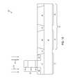
- a substrate 110is formed with a plurality of isolation features 111 , 112 .
- the substrate 110comprises an elementary semiconductor, a compound semiconductor, an alloy semiconductor, or combinations thereof.
- the elementary semiconductorinclude, but are not limited to, silicon and germanium.
- a compound semiconductorinclude, but are not limited to, silicon carbide, gallium arsenic, gallium phosphide, indium phosphide, indium arsenide, and indium antimonide.
- the alloy semiconductorinclude, but are not limited to, SiGe, GaAsP, AlInAs, AlGaAs, GaInAs, GaInP, and GaInAsP.
- the substrate 110comprises a semiconductor on insulator (SOI), a doped epitaxial layer, a gradient semiconductor layer, and/or a stacked semiconductor structure with one semiconductor layer (e.g., Si) overlying another semiconductor layer (e.g., Ge) of a different type.
- SOIsemiconductor on insulator
- one semiconductor layere.g., Si
- Geanother semiconductor layer
- the isolation features 111 , 112are formed at least partially in the substrate 110 .
- the isolation features 111 , 112include raised structures partially located outside the substrate 110 .
- the isolation features 111 , 112utilize isolation technology, such as local oxidation of silicon (LOCOS) and/or shallow trench isolation (STI), to define and electrically isolate various regions of the substrate 110 from each other.
- the isolation features 111 , 112comprise silicon oxide, silicon nitride, silicon oxynitride, other suitable materials, or combinations thereof.
- the isolation features 111 , 112are formed by a suitable process.
- the formation of an STIcomprises a photolithography process, etching a trench in the substrate 110 , and filling the trench, for example, by using a chemical vapor deposition (CVD) process with one or more dielectric materials.
- the filled trenchhas a multi-layer structure, such as a thermal oxide liner layer filled with silicon nitride or silicon oxide.
- the isolation features 111 , 112isolate various regions of the substrate 110 from each other.
- one or more isolation features 111isolate an input/output (I/O) device region 113 of the substrate 110 from a core device region 114 of the substrate 110 .
- the core device region 114includes circuitry formed of core devices which are the devices having the thinnest gate dielectric layer, fastest speed and lowest nominal operating voltage in the semiconductor device.
- the I/O device region 113includes I/O devices which are configured to input and output data to and from the circuitry in the core device region 114 , and to exchange data with a peripheral device either in the semiconductor device or external to the semiconductor device.
- the peripheral deviceincludes at least one embedded flash cell formed over the substrate 110 .
- the I/O deviceshave a higher nominal operating voltage than the core devices.
- One or more isolation features 112are formed inside the core device region 114 , and isolate a region 115 for at least one core device with a higher threshold voltage (hereinafter “HVt device”) from a region 116 for at least one core device with a lower threshold voltage (hereinafter “LVt device”).
- HVt devicea region 115 for at least one core device with a higher threshold voltage
- LVt devicea region 116 for at least one core device with a lower threshold voltage
- the HVt and LVt devicesare both core devices and have the same nominal operating voltage. However, the HVt and LVt devices are configured to have different threshold voltages depending on the circuit design and/or application.
- the HVt devicescomprise devices with different levels of threshold voltages which are referred to as high threshold voltage devices and ultra-high threshold voltage devices in some situations.
- the LVt devicescomprise devices with different levels of threshold voltages which are referred to as standard threshold voltage devices, low threshold voltage devices and ultra-low threshold voltage devices in some situations.
- One or more isolation featuresfurther isolate regions for p-type devices from regions for n-type devices.
- a p-type deviceis a device configured to have holes as charge carriers.
- An example of a p-type deviceis a PMOS transistor.
- An n-type deviceis a device configured to have electrons as charge carriers.
- An example of an n-type deviceis an NMOS transistor.
- all regions 113 , 115 , and 116 indicated in FIG. 1Aare for the same type of devices. In one example, all devices in the regions 113 , 115 , and 116 are PMOS devices. In another example, all devices in the regions 113 , 115 , and 116 are NMOS devices.
- the isolation features 111 , 112define active regions 117 , 118 in the corresponding I/O device region 113 and core device region 114 .
- one or more of the active regions 117 , 118include doped regions.
- a p-type doped regioncomprises one or more p-type dopants, such as boron or BF 2 .
- An n-type doped regioncomprises one or more n-type dopants, such as phosphorus or arsenic.
- doped regionsare formed directly on the substrate 110 , in a P-well structure, an N-well structure, a dual-well structure, or a raised structure.
- the active region 117 of an I/O deviceis configured to be different from the active regions 118 of the HVt and LVt devices, for example, by performing different doping operations in the active region 117 and in the active regions 118 .
- the active regions 118 of the HVt and LVt devicesare configured to be the same.
- a gate structure 120 of an I/O deviceis formed over the substrate 110 in the I/O device region 113 .
- the gate structure 120comprises a gate dielectric layer 121 , a gate electrode 122 , and a hard mask layer 123 .
- Other layersare included in some embodiments.
- the gate structure 120is formed by CVD, physical vapor deposition (PVD), atomic layer deposition (ALD), high density plasma CVD (HDPCVD), plating, other suitable methods, or combinations thereof.
- the gate dielectric layer 121is formed over the substrate 110 and comprises a dielectric material, a high-k dielectric material, other suitable dielectric material, or combinations thereof.
- a dielectric materialinclude, but are not limited to, silicon oxide, silicon oxynitride, silicon nitride, or combinations thereof.
- high-k dielectric materialsinclude, but are not limited to, HfO 2 , HfSiO, HfSiON, HfTaO, HfTiO, HfZrO, or combinations thereof.
- the gate dielectric layer 121comprises a multilayer structure.
- the gate dielectric layer 121comprises an interfacial layer, and a high-k dielectric material layer formed on the interfacial layer.
- An exemplary interfacial layeris a grown silicon oxide layer formed by a thermal process or ALD process.
- the gate electrode 122is formed over the gate dielectric layer 121 .
- the gate electrode 122is a polycrystalline silicon (polysilicon) layer.
- the polysilicon layeris doped for proper conductivity, e.g., in a gate-first process.
- the polysiliconis not doped where it is a dummy gate to be replaced in a subsequent gate replacement (gate last) process.
- the gate electrode 122comprises a conductive layer having a proper work function.
- a p-type work function metalcomprises TiN, TaN and/or a carbon-doped metal nitride such as TaCN
- an n-type work function metalcomprises Ta, TiAl, and/or TiAlN—.
- the work function layercomprises doped conducting oxide materials.
- the gate electrode 122comprises other conductive materials, such as aluminum, copper, tungsten, metal alloys, metal silicide, other suitable materials, or combinations thereof. For example, where the gate electrode 122 comprises a work function layer, another conductive layer is formed over the work function layer.
- the hard mask layer 123is formed over the gate electrode 122 to function as an etch mask, and/or to protect the underlying layers from damage during subsequent processing.
- the hard mask layer 123comprises silicon oxide, silicon nitride, silicon oxynitride, silicon carbide, or combinations thereof.
- the described structure of the gate structure 120is an example. Other gate structure configurations are within the scope of various embodiments.
- the regions of the I/O device region 113 outside the gate structure 120are doped with dopants 124 to form lightly doped source/drain (LDD) regions 125 .
- the dopantsare selected depending on the type of the devices to be formed in the LDD regions 125 .
- LDD regions for forming NMOS devicesare doped with an n-type dopant, such as phosphorous or arsenic
- LDD regions for forming PMOS devicesare doped with a p-type dopant, such as boron or BF 2 .
- a resulting structure 100 Ais obtained upon formation of the LDD regions 125 .
- dummy spacers 126are formed over sidewalls of the gate structure 120 .
- the dummy spacers 126comprise a nitride material, such as silicon nitride, silicon oxide, silicon oxynitride, or combinations thereof.
- a lineris formed over the sidewalls of the gate structure 120 before the spacers 126 are formed.
- such a linercomprises an oxide material, such as silicon oxide and/or another suitable dielectric material.
- the liner and the dummy spacers 126are formed by blanket depositing a first dielectric layer for defining the liner over the structure 100 A, and a second dielectric layer for defining the dummy spacers 126 over the first dielectric layer. The dielectric layers are then anisotropically etched to form the liner and the dummy spacers 126 .
- a selective ion implantationis performed to adjust the threshold voltage of the HVt device in the HVt device region 115 to be higher than the threshold voltage of the LVt device in the LVt device region 116 .
- the HVt device to be formedis a PMOS transistor
- n-type dopants 128such as phosphorous
- the presence of n-type dopants 128 in the active region 118 of a PMOS transistordecreases the number of holes (which are charge carriers of the PMOS transistor) available in a channel region of the PMOS transistor.
- the threshold voltage of the PMOS transistoris increased.
- the HVt device to be formedis an NMOS transistor
- p-type dopantssuch as boron
- the dopants 128are implanted in the active region 118 of the HVt device, and are not implanted in the active region 118 of the LVt device.
- the dopants 128are implanted in the active regions 118 of both the HVt and LVt devices, and with a higher concentration of the dopants 128 in the active region 118 of the HVt device than in the active region 118 of the LVt device.
- the described threshold voltage adjustment through ion implantationis an example. Other threshold voltage adjustment arrangements are within the scope of various embodiments. A resulting structure 100 B is obtained upon completion of the threshold voltage adjustment.
- gate structures 130 H and 130 Lare formed over the structure 100 B, in the active regions 118 of the HVt and LVt devices.
- the gate structure 130 Hhas a narrower width (or gate length) than the gate structure 120 , resulting in a HVt device (which is a core device) having a smaller size than the I/O device corresponding to the gate structure 120 .
- the gate structure 130 Lhas a narrower width (or gate length) than the gate structure 120 , resulting in a LVt device (which is a core device) having a smaller size than the I/O device corresponding to the gate structure 120 .
- the gate structures 130 H and 130 Lare configured to have the same configuration comprising a gate dielectric layer 131 , a gate electrode 132 and a hard mask layer 133 .
- one or more of the described materials of and/or processes for forming the gate dielectric layer 121 , gate electrode 122 and hard mask layer 123are applicable to the corresponding gate dielectric layer 131 , gate electrode 132 and hard mask layer 133 .
- the gate dielectric layers 131 of the gate structures 130 H and 130 Lhave the same dielectric material of the same thickness which is thinner than the gate dielectric layer 121 of the I/O device, resulting in the corresponding core devices having a faster speed and/or a lower nominal operating voltage than the I/O device.
- the regions of the core device region 114 outside the gate structures 130 H and 130 Lare doped to form LDD regions (not indicated in the figures).
- LDD regionsare doped to form LDD regions (not indicated in the figures).
- One or more of the described materials of and/or processes for forming the LDD regions 125 in the I/O device region 113are applicable to the LDD regions in the core device region 114 .
- Dummy spacers 136are formed over sidewalls of the gate structures 130 H and 130 L.
- the spacers 136are formed after the formation of the LDD regions in the core device region 114 .
- one or more of the described materials of and/or processes for forming the spacers 126are applicable to the spacers 136 .
- a resulting structure 100 Cis obtained upon formation of the gate structures 130 H and 130 L and the spacers 126 .
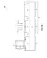
- a sacrificial layer 140is formed over the structure 100 C, and covers the I/O device region 113 and the core device region 114 including the gate structures 120 , 130 H, 130 L formed thereover.
- the sacrificial layer 140includes SiN. Other materials are within the scope of various embodiments.
- a photoresist layer 142is formed over the sacrificial layer 140 .
- the photoresist layer 142covers the I/O device region 113 and the HVt device region 115 , without covering the LVt device region 116 .
- at least one embedded flash cellis formed over the substrate 110 , and the sacrificial layer 140 and photoresist layer 142 cover the embedded flash cell.
- a resulting structure 100 Dis obtained upon formation of the sacrificial layer 140 and the photoresist layer 142 .
- a stressoris formed in at least one of a source region or a drain region of the LVt device in the LVt device region 116 which is not covered by the photoresist layer 142 .
- the stressoris configured to enhance charge carrier mobility in the at least one source or drain region.
- the stressoris configured to apply a compressive stress to enhance hole mobility in the at least one source or drain region of the PMOS device.
- the stressoris configured to apply a tensile stress to enhance electron mobility in the at least one source or drain region of the PMOS device.
- the stressor materialexamples include, but are not limited to, SiGe, SiC, GeSn, SiGeSn, and other suitable materials.
- the stressor for a PMOS devicecomprises SiGe.
- the stressor for an NMOS devicecomprises SiC.
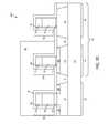
- the stressor formationcomprises an etching process and a deposition process.
- the etching processis performed to remove portions of the sacrificial layer 140 and the substrate 110 outside the gate structure 130 L and the isolation feature 112 to form recesses in the substrate 110 , corresponding source and drain regions of the LVt device.
- the recessesare formed in the LDD regions 125 previously formed in the LVt device region 116 .
- the etching processcomprises a dry etching process, a wet etching process, or combinations thereof.
- a semiconductor materialis deposited in the recesses to form stressors 144 in the source and drain regions of the LVt device.
- an epitaxial processis performed to deposit the semiconductor material in the recesses.
- the epitaxial processinclude, but are not limited to, a selective epitaxy growth (SEG) process, CVD deposition techniques (e.g., vapor-phase epitaxy (VPE) and/or ultra-high vacuum CVD (UHV-CVD)), molecular beam epitaxy, other suitable epitaxial processes, or combinations thereof.
- the epitaxial processuses gaseous and/or liquid precursors, which interact with the composition of the substrate 110 .
- the grown stressors 144are raised above an upper surface of the substrate 110 and are higher than corresponding source and drain regions of the HVt device in the HVt device region 115 . In some embodiments, the stressors 144 are grown to have an upper surface flush with or lower than the upper surface of the substrate 110 .
- a resulting structure 100 Eis obtained upon removal of the sacrificial layer 140 and the photoresist layer 142 .
- main spacers 146are formed over the dummy spacers 126 , 136 .
- the spacers 146are formed by blanket depositing a dielectric layer over the structure 100 E, and then anisotropically etching to remove the dielectric layer to form the spacers 146 .
- the spacers 146comprise a dielectric material, such as silicon nitride, silicon oxide, silicon oxynitride, other suitable materials, or combinations thereof.
- the dummy spacers 126 and/or 136are removed before the formation of the main spacers 146 .
- the dummy spacers 126 and/or 136are removed by a wet etching using phosphoric acid or hydrofluoric acid, or by a dry etching using a suitable etchant.
- the source and drain regions 154 , 164 H and 164 Lare formed in the corresponding I/O device region 113 , HVt device region 115 and LVt device region 116 .
- the source and drain regions 154 and 164 Hare formed by doping the substrate 110 outside the corresponding gate structure 120 and gate structure 130 H
- the source and drain regions 164 Lare formed by doping the stressors 144 outside the corresponding gate structure 130 L with dopants in an ion implantation process, a plasma immersion ion implantation (PIII) process, a gas and/or solid source diffusion process, other suitable process, or combinations thereof.
- PIIIplasma immersion ion implantation
- a resulting semiconductor device 100 Fcomprises an I/O device 159 , a HVt device 169 H and a LVt device 169 L.
- the I/O device 159comprises the gate structure 120 , the corresponding main spacers 146 over the sidewalls of the gate structure 120 , and the source and drain regions 154 all formed over the active region 117 in the I/O device region 113 .
- the HVt device 169 Hcomprises the gate structure 130 H, the corresponding main spacers 146 over the sidewalls of the gate structure 130 H, and the source and drain regions 164 H all formed over the active region 118 in the HVt device region 115 of the core device region 114 .
- the LVt device 169 Lcomprises the gate structure 130 L, the corresponding main spacers 146 over the sidewalls of the gate structure 130 L, and the source and drain regions 164 L with stressors 144 , all formed over the active region 118 in the LVt device region 116 of the core device region 114 .
- the semiconductor device 100 Ffurther includes silicide features formed on the source and drain regions 154 , 164 H and/or 164 L to reduce electrical resistance with the contact.
- the silicide featuresare formed, for example, by depositing a metal layer, annealing the metal layer such that the metal layer reacts with silicon to form silicide, and then removing the non-reacted metal layer.
- the semiconductor device 100 Ffurther includes an inter-level dielectric (ILD) layer formed over the substrate 110 , and a chemical mechanical polishing (CMP) process is further applied to planarize the ILD layer.
- the gate electrodes 122 and/or 132remain polysilicon in a gate first process.
- the polysiliconis removed and replaced with a metal in a gate last or gate replacement process.
- a gate last processthe CMP process on the ILD layer is continued to expose the polysilicon of the gate structures 120 and/or 130 H and/or 130 L, and an etching process is performed to remove the polysilicon, thereby forming trenches.
- the trenchesare filled with a proper work function metal (e.g., p-type work function metal and n-type work function metal) for corresponding p-type devices and n-type devices, respectively.
- a multilayer interconnectionincluding metal layers and inter-metal dielectric (IMD) is formed over the semiconductor device 100 F to electrically connect various features or structures of the semiconductor device 100 F.
- the multilayer interconnectionincludes vertical interconnects, such as vias or contacts, and horizontal interconnects, such as metal lines.
- the various interconnection featuresmay implement various conductive materials including copper, tungsten, silicide, and/or some metal alloys.
- a damascene processis used to form a copper multilayer interconnection structure and one or more metal alloys are deposited as a barrier for such a multilayer structure in the damascene process.
- some embodimentsinclude I/O devices and core devices. Such an arrangement is an example. Other arrangements are within the scope of various embodiments. For example, at least one embodiment, I/O devices and the corresponding I/O region are omitted. For another example, in at least one embodiment, the HVt device 169 H and the LVt device 169 L are not core devices.
- the HVt device 169 Hhas a higher threshold voltage than the LVt device 169 L, and the LVt device 169 L includes stressors 144 which are not formed in the HVt device 169 H.
- carrier mobilityis higher in the LVt device 169 L than in the HVt device 169 H due to the presence of the stressors 144
- leakage currentwhich is associated with carrier mobility, is lower in the HVt device 169 H due to the absence of stressors.
- Such an arrangement in at least one embodimentpermits flexibility in circuit design with enhanced performance obtained at some devices, e.g., the LVt devices, and current leakage reduction provided at other devices, e.g., the HVt devices.
- applications where such an arrangement is advantageousinclude, but are not limited to, automotive and mobile applications where leakage current is a consideration.
- implantation tuningis employed, but is insufficient to meet low leakage requirements in some applications.
- the gate lengthis increased to lower current leakage at the expense of increased die area.
- semiconductor devices in accordance with one or more embodimentshave leakage current reduced to a level sufficient to meet low leakage requirements in some applications, without increasing the device size and/or chip area.
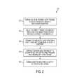
- FIG. 2is a flow chart of a method 200 of manufacturing a semiconductor device in accordance with some embodiments.
- isolation features, active regions, and a gate structure for an I/O deviceare formed over a semiconductor substrate.
- isolation features 111 , 112 , active regions 117 , 118 , and a gate structure 120 for an I/O deviceare formed over a semiconductor substrate 110 , as described with respect to FIG. 1A .
- a first threshold voltage of a first core deviceis adjusted to be higher than a second threshold voltage of a second core device.
- the threshold voltage of a first core device to be formed over the active region 118 in the HVt device region 115is adjusted to be higher than the threshold voltage of a second core device to be formed over the active region 118 in LVt device region 116 .
- An example threshold voltage adjustmentincludes ion implantation, as described with respect to FIG. 1B .
- first and second gate structures for the first and second core devicesare formed over the semiconductor substrate.
- gate structures 130 H and 130 L for the corresponding HVt device and LVt deviceare formed over the substrate 110 in the corresponding active regions 118 , as described with respect to FIG. 1C .
- stressorsare formed in source and drain regions of the second core device, without forming stressors in source and drain regions of the first core device.
- stressors 144are formed in source and drain regions of the LVt device, without forming stressors in source and drain regions of the HVt device, as described with respect to FIGS. 1D-1E .
- spacers and source and drain regions of the I/O device and the core devicesare formed.
- spacers 146 and source and drain regions 154 , 164 H and 164 L of the corresponding I/O device 159 , HVt device 169 H and LVt device 169 Lare formed, as described with respect to FIG. 1F .
- the method described herein in accordance with some embodimentsis useful for manufacturing semiconductor devices using technology nodes at 40 nm and below.
- the method described herein in accordance with some embodimentsis also useful for manufacturing semiconductor devices using technology nodes above 40 nm.
- FIG. 3is a diagram showing a mask generation operation 300 in a method of manufacturing a semiconductor device in accordance with some embodiments.
- the mask generation operation 300is arranged to generate a mask for selectively forming stressors in some devices, e.g., LVt devices in the LVt device region 116 , but not in other devices, e.g., the HVt devices in the HVt device region 115 .
- a layout of the semiconductor device to be manufacturedincludes a HVt device region 315 for HVt devices, and a LVt device region 316 for LVt devices.
- the HVt device region 315 and LVt device region 316correspond to the HVt device region 115 and LVt device region 116 as described herein.
- a mask 372is used for an ion implantation to adjust a threshold voltage of the HVt devices to be higher than a threshold voltage of the LVt devices.
- the mask 372covers the HVt device region 315 and permits a patterned photoresist layer to be formed over the LVt device region 316 in a photolithography process using the mask 372 .
- the patterned photoresist layercovers the LVt device region 316 , without covering the HVt device region 315 , and permits an ion implantation to be performed in the HVt device region 315 , but not in the LVt device region 316 , for example, as described herein with respect to FIG. 1B .
- a mask 374is to be used in accordance with another approach to form stressors in both the HVt devices and the LVt devices.
- the mask 374covers the HVt device region 315 and the LVt device region 316 .
- the mask 374permits a patterned photoresist layer formed in a photolithography process using the mask 374 to expose both the HVt device region 315 and the LVt device region 316 .
- the patterned photoresist layerpermits stressors to be formed for both HVt devices and LVt devices in accordance with the another approach.
- a mask 376is obtained by performing at least one logic operation (LOP) on the mask 372 and the mask 374 .
- LOPlogic operation
- an XOR operationis performed on the mask 372 and the mask 374 to obtain the mask 376 .
- Other LOPssuch as, AND, OR, NOT, NOR, NAND and bias (sizing) are within the scope of various embodiments.
- more than one LOPsare performed to generate the mask 376 .
- the mask 376covers the LVt device region 316 and permits a patterned photoresist layer, such as the photoresist layer 142 described with respect to FIG. 1D , to be formed over the HVt device region 315 in a photolithography process using the mask 376 .
- the patterned photoresist layercovers the HVt device region 315 , without covering the LVt device region 316 , and permits a stressor formation, such as an epitaxial growth described herein with respect to FIG. 1E , to be performed in the LVt device region 316 but not in the HVt device region 315 .
- the mask generation operation 300is a simple modification to change a manufacturing process in accordance with another approach which forms stressors in all core devices to a manufacturing process in accordance with some embodiments which selectively form stressors in LVt devices, but not in HVt devices.
- the mask generation operation 300is performed by one or more processors and/or application specific integrated circuits (ASICs).
- some embodimentsform stressors in devices with lower threshold voltages, but not in devices with higher threshold voltages.
- enhanced carrier mobility and device performanceare obtainable for the devices with lower threshold voltages.
- leakage currentis reduced which is preferred in some applications, such as automotive and mobile applications.
- reduced leakage currentis obtainable in accordance with some embodiments by adding a simple LOP to a manufacturing process in accordance with another approach.
- a semiconductor devicecomprises a semiconductor substrate, and a first transistor and a second transistor over the semiconductor substrate. Both the first and second transistors are p-type transistors or both the first and second transistors are n-type transistors. The first and second transistors have the same nominal operating voltage. The first transistor has a higher threshold voltage than the second transistor. The second transistor has at least one of a source region or a drain region with higher charge carrier mobility than at least one of a source region or a drain region of the first transistor.
- a semiconductor devicecomprises a semiconductor substrate, and a first transistor and a second transistor over the semiconductor substrate. Both the first and second transistors are p-type transistors or both the first and second transistors are n-type transistors.
- the first and second transistorshave corresponding first and second gate dielectric layers, the first and second gate dielectric layers comprising the same dielectric material and having the same thickness.
- a channel region of the first transistor and a channel region of the second transistorcomprise different concentrations of a dopant.
- a source region and a drain region of the second transistorcomprise a stressor, the stressor configured to apply a tensile stress or a compressive stress to the source region and the drain region of the second transistor.
- a source region and a drain region of the first transistorare free of the stressor.
- first and second gate structures of corresponding first and second core devicesare formed over a semiconductor substrate, and a stressor is formed in source and drain regions of the second core device, but not in source and drain regions of the first core device.
- Both the first and second core devicesare p-type devices or both the first and second core devices are n-type devices.
Landscapes
- Physics & Mathematics (AREA)
- Engineering & Computer Science (AREA)
- High Energy & Nuclear Physics (AREA)
- Microelectronics & Electronic Packaging (AREA)
- Condensed Matter Physics & Semiconductors (AREA)
- General Physics & Mathematics (AREA)
- Manufacturing & Machinery (AREA)
- Computer Hardware Design (AREA)
- Power Engineering (AREA)
- Toxicology (AREA)
- Health & Medical Sciences (AREA)
- Metal-Oxide And Bipolar Metal-Oxide Semiconductor Integrated Circuits (AREA)
- Insulated Gate Type Field-Effect Transistor (AREA)
Abstract
Description
- The recent trend in miniaturizing integrated circuits (ICs) has resulted in smaller devices which consume less power, yet provide more functionally at higher speeds than before. For these advantages to be realized, various developments in IC manufacturing are developed. For example, as semiconductor devices, such as metal-oxide-semiconductor field-effect transistors (MOSFETs), are scaled down, source and drain regions of MOSFETs are formed with stressors to enhance carrier mobility and improve device performance.
- Aspects of the present disclosure are best understood from the following detailed description when read with the accompanying figures. It is noted that, in accordance with the standard practice in the industry, various features are not drawn to scale. In fact, the dimensions of the various features may be arbitrarily increased or reduced for clarity of discussion.
FIGS. 1A-1F are schematic cross-sectional views of a semiconductor device in various manufacturing operations in accordance with some embodiments.FIG. 2 is a flow chart of a method of manufacturing a semiconductor device in accordance with some embodiments.FIG. 3 is a diagram showing a mask generation operation in a method of manufacturing a semiconductor device in accordance with some embodiments.- The following disclosure provides many different embodiments, or examples, for implementing different features of the invention. Specific examples of components and arrangements are described below to simplify the present disclosure. These are, of course, merely examples and are not intended to be limiting. For example, the formation of a first feature over or on a second feature in the description that follows may include embodiments in which the first and second features are formed in direct contact, and may also include embodiments in which additional features may be formed between the first and second features, such that the first and second features may not be in direct contact. In addition, the present disclosure may repeat reference numerals and/or letters in the various examples. This repetition is for the purpose of simplicity and clarity and does not in itself dictate a relationship between the various embodiments and/or configurations discussed.
- Further, spatially relative terms, such as “beneath,” “below,” “lower,” “above,” “upper” and the like, may be used herein for ease of description to describe one element or feature's relationship to another element(s) or feature(s) as illustrated in the figures. The spatially relative terms are intended to encompass different orientations of the device in use or operation in addition to the orientation depicted in the figures. The apparatus may be otherwise oriented (rotated 90 degrees or at other orientations) and the spatially relative descriptors used herein may likewise be interpreted accordingly.
- In some embodiments, stressors are formed in devices or transistors with lower threshold voltages, but are not formed in devices or transistors with higher threshold voltages. As a result, enhanced carrier mobility and device performance are obtainable for the devices or transistors with lower threshold voltages. In the devices or transistors with higher threshold voltages, leakage current, which is associated with carrier mobility, is reduced due to the absence of stressors. The reduced leakage current in devices or transistors with higher threshold voltages is preferred over enhanced carrier mobility in at least one embodiment.
FIGS. 1A-1F are schematic cross-sectional views of a semiconductor device in various manufacturing operations in accordance with some embodiments.- In one or more embodiments, the semiconductor device comprises active components such as field effect transistors (FET), complementary metal-oxide-semiconductor (CMOS) transistors, metal-oxide-semiconductor field effect transistors (MOSFETs), high voltage transistors, high frequency transistors, and combinations thereof. In one or more embodiments, the semiconductor device comprises passive components, such as resistors, capacitors, inductors, and fuses. In the description below, p-channel metal-oxide semiconductor (PMOS) and/or n-channel metal-oxide semiconductor (NMOS) devices are described. However, further embodiments are applicable to other types of semiconductor devices or components.
- In the operation in
FIG. 1A , asubstrate 110 is formed with a plurality of isolation features111,112. In some embodiments, thesubstrate 110 comprises an elementary semiconductor, a compound semiconductor, an alloy semiconductor, or combinations thereof. Examples of the elementary semiconductor include, but are not limited to, silicon and germanium. Examples of a compound semiconductor include, but are not limited to, silicon carbide, gallium arsenic, gallium phosphide, indium phosphide, indium arsenide, and indium antimonide. Examples of the alloy semiconductor include, but are not limited to, SiGe, GaAsP, AlInAs, AlGaAs, GaInAs, GaInP, and GaInAsP. Other semiconductor materials including group III, group IV, and group V elements are used in some embodiments. In one or more embodiments, thesubstrate 110 comprises a semiconductor on insulator (SOI), a doped epitaxial layer, a gradient semiconductor layer, and/or a stacked semiconductor structure with one semiconductor layer (e.g., Si) overlying another semiconductor layer (e.g., Ge) of a different type. - The isolation features111,112 are formed at least partially in the
substrate 110. In some embodiments, the isolation features111,112 include raised structures partially located outside thesubstrate 110. The isolation features111,112 utilize isolation technology, such as local oxidation of silicon (LOCOS) and/or shallow trench isolation (STI), to define and electrically isolate various regions of thesubstrate 110 from each other. In some embodiments, the isolation features111,112 comprise silicon oxide, silicon nitride, silicon oxynitride, other suitable materials, or combinations thereof. The isolation features111,112 are formed by a suitable process. In one example, the formation of an STI comprises a photolithography process, etching a trench in thesubstrate 110, and filling the trench, for example, by using a chemical vapor deposition (CVD) process with one or more dielectric materials. In one or more embodiments, the filled trench has a multi-layer structure, such as a thermal oxide liner layer filled with silicon nitride or silicon oxide. - The isolation features111,112 isolate various regions of the
substrate 110 from each other. For example, one or more isolation features111 (one of which is indicated inFIG. 1A for simplicity) isolate an input/output (I/O)device region 113 of thesubstrate 110 from acore device region 114 of thesubstrate 110. Thecore device region 114 includes circuitry formed of core devices which are the devices having the thinnest gate dielectric layer, fastest speed and lowest nominal operating voltage in the semiconductor device. The I/O device region 113 includes I/O devices which are configured to input and output data to and from the circuitry in thecore device region 114, and to exchange data with a peripheral device either in the semiconductor device or external to the semiconductor device. In at least one embodiment, the peripheral device includes at least one embedded flash cell formed over thesubstrate 110. The I/O devices have a higher nominal operating voltage than the core devices. - One or more isolation features112 (one of which is indicated in
FIG. 1A for simplicity) are formed inside thecore device region 114, and isolate aregion 115 for at least one core device with a higher threshold voltage (hereinafter “HVt device”) from aregion 116 for at least one core device with a lower threshold voltage (hereinafter “LVt device”). The HVt and LVt devices are both core devices and have the same nominal operating voltage. However, the HVt and LVt devices are configured to have different threshold voltages depending on the circuit design and/or application. In at least one embodiment, the HVt devices comprise devices with different levels of threshold voltages which are referred to as high threshold voltage devices and ultra-high threshold voltage devices in some situations. In at least one embodiment, the LVt devices comprise devices with different levels of threshold voltages which are referred to as standard threshold voltage devices, low threshold voltage devices and ultra-low threshold voltage devices in some situations. - One or more isolation features (not indicated in
FIG. 1A ) further isolate regions for p-type devices from regions for n-type devices. A p-type device is a device configured to have holes as charge carriers. An example of a p-type device is a PMOS transistor. An n-type device is a device configured to have electrons as charge carriers. An example of an n-type device is an NMOS transistor. In the following description, allregions FIG. 1A are for the same type of devices. In one example, all devices in theregions regions - The isolation features111,112 define
active regions O device region 113 andcore device region 114. In some embodiments, one or more of theactive regions substrate 110, in a P-well structure, an N-well structure, a dual-well structure, or a raised structure. When a p-type doped region is being formed, n-type doped regions or regions to be doped with n-type dopants are protected, for example, by one or more protective layers, such as photoresist layers, and vice versa. In at least one embodiment, theactive region 117 of an I/O device is configured to be different from theactive regions 118 of the HVt and LVt devices, for example, by performing different doping operations in theactive region 117 and in theactive regions 118. In at least one embodiment, theactive regions 118 of the HVt and LVt devices are configured to be the same. - A
gate structure 120 of an I/O device is formed over thesubstrate 110 in the I/O device region 113. Thegate structure 120 comprises agate dielectric layer 121, agate electrode 122, and ahard mask layer 123. Other layers are included in some embodiments. In some embodiments, thegate structure 120 is formed by CVD, physical vapor deposition (PVD), atomic layer deposition (ALD), high density plasma CVD (HDPCVD), plating, other suitable methods, or combinations thereof. - The
gate dielectric layer 121 is formed over thesubstrate 110 and comprises a dielectric material, a high-k dielectric material, other suitable dielectric material, or combinations thereof. Examples of a dielectric material include, but are not limited to, silicon oxide, silicon oxynitride, silicon nitride, or combinations thereof. Examples of high-k dielectric materials include, but are not limited to, HfO2, HfSiO, HfSiON, HfTaO, HfTiO, HfZrO, or combinations thereof. In some embodiments, thegate dielectric layer 121 comprises a multilayer structure. For example, thegate dielectric layer 121 comprises an interfacial layer, and a high-k dielectric material layer formed on the interfacial layer. An exemplary interfacial layer is a grown silicon oxide layer formed by a thermal process or ALD process. - The
gate electrode 122 is formed over thegate dielectric layer 121. In one or more embodiments, thegate electrode 122 is a polycrystalline silicon (polysilicon) layer. In one or more embodiments, the polysilicon layer is doped for proper conductivity, e.g., in a gate-first process. In one or more embodiments, the polysilicon is not doped where it is a dummy gate to be replaced in a subsequent gate replacement (gate last) process. In one or more embodiments, thegate electrode 122 comprises a conductive layer having a proper work function. For example, a p-type work function metal (p-metal) comprises TiN, TaN and/or a carbon-doped metal nitride such as TaCN, whereas an n-type work function metal (n-metal) comprises Ta, TiAl, and/or TiAlN—. In one or more embodiments, the work function layer comprises doped conducting oxide materials. In one or more embodiments, thegate electrode 122 comprises other conductive materials, such as aluminum, copper, tungsten, metal alloys, metal silicide, other suitable materials, or combinations thereof. For example, where thegate electrode 122 comprises a work function layer, another conductive layer is formed over the work function layer. - The
hard mask layer 123 is formed over thegate electrode 122 to function as an etch mask, and/or to protect the underlying layers from damage during subsequent processing. In one or more embodiments, thehard mask layer 123 comprises silicon oxide, silicon nitride, silicon oxynitride, silicon carbide, or combinations thereof. The described structure of thegate structure 120 is an example. Other gate structure configurations are within the scope of various embodiments. - The regions of the I/
O device region 113 outside thegate structure 120 are doped withdopants 124 to form lightly doped source/drain (LDD)regions 125. The dopants are selected depending on the type of the devices to be formed in theLDD regions 125. For example, LDD regions for forming NMOS devices are doped with an n-type dopant, such as phosphorous or arsenic, and LDD regions for forming PMOS devices are doped with a p-type dopant, such as boron or BF2. A resultingstructure 100A is obtained upon formation of theLDD regions 125. - In the operation in
FIG. 1B ,dummy spacers 126 are formed over sidewalls of thegate structure 120. In at least one embodiment, thedummy spacers 126 comprise a nitride material, such as silicon nitride, silicon oxide, silicon oxynitride, or combinations thereof. In some embodiments, a liner is formed over the sidewalls of thegate structure 120 before thespacers 126 are formed. In at least one embodiment, such a liner comprises an oxide material, such as silicon oxide and/or another suitable dielectric material. In at least one embodiment, the liner and thedummy spacers 126 are formed by blanket depositing a first dielectric layer for defining the liner over thestructure 100A, and a second dielectric layer for defining thedummy spacers 126 over the first dielectric layer. The dielectric layers are then anisotropically etched to form the liner and thedummy spacers 126. - A selective ion implantation is performed to adjust the threshold voltage of the HVt device in the
HVt device region 115 to be higher than the threshold voltage of the LVt device in theLVt device region 116. For example, when the HVt device to be formed is a PMOS transistor, n-type dopants 128, such as phosphorous, are implanted into theactive region 118 of the HVt device in theHVt device region 115, to form the n-dopedregion 129. The presence of n-type dopants 128 in theactive region 118 of a PMOS transistor decreases the number of holes (which are charge carriers of the PMOS transistor) available in a channel region of the PMOS transistor. Since fewer holes are available, a higher gate voltage is to be applied for switching the PMOS transistor, i.e., the threshold voltage of the PMOS transistor is increased. When the HVt device to be formed is an NMOS transistor, p-type dopants, such as boron, are implanted into theactive region 118 of the HVt device. The higher the concentration of thedopants 128, the higher the threshold voltage of the HVt device. In some embodiments, thedopants 128 are implanted in theactive region 118 of the HVt device, and are not implanted in theactive region 118 of the LVt device. In some embodiments, thedopants 128 are implanted in theactive regions 118 of both the HVt and LVt devices, and with a higher concentration of thedopants 128 in theactive region 118 of the HVt device than in theactive region 118 of the LVt device. The described threshold voltage adjustment through ion implantation is an example. Other threshold voltage adjustment arrangements are within the scope of various embodiments. A resultingstructure 100B is obtained upon completion of the threshold voltage adjustment. - In the operation in
FIG. 1C ,gate structures structure 100B, in theactive regions 118 of the HVt and LVt devices. In at least one embodiment, thegate structure 130H has a narrower width (or gate length) than thegate structure 120, resulting in a HVt device (which is a core device) having a smaller size than the I/O device corresponding to thegate structure 120. Similarly, thegate structure 130L has a narrower width (or gate length) than thegate structure 120, resulting in a LVt device (which is a core device) having a smaller size than the I/O device corresponding to thegate structure 120. - In at least one embodiment, the
gate structures gate dielectric layer 131, agate electrode 132 and ahard mask layer 133. In some embodiments, one or more of the described materials of and/or processes for forming thegate dielectric layer 121,gate electrode 122 andhard mask layer 123 are applicable to the correspondinggate dielectric layer 131,gate electrode 132 andhard mask layer 133. In at least one embodiment, the gatedielectric layers 131 of thegate structures gate dielectric layer 121 of the I/O device, resulting in the corresponding core devices having a faster speed and/or a lower nominal operating voltage than the I/O device. - In some embodiments, the regions of the
core device region 114 outside thegate structures LDD regions 125 in the I/O device region 113 are applicable to the LDD regions in thecore device region 114. Dummy spacers 136 are formed over sidewalls of thegate structures spacers 136 are formed after the formation of the LDD regions in thecore device region 114. In at least one embodiment, one or more of the described materials of and/or processes for forming thespacers 126 are applicable to thespacers 136. A resultingstructure 100C is obtained upon formation of thegate structures spacers 126.- In the operation in
FIG. 1D , asacrificial layer 140 is formed over thestructure 100C, and covers the I/O device region 113 and thecore device region 114 including thegate structures sacrificial layer 140 includes SiN. Other materials are within the scope of various embodiments. Aphotoresist layer 142 is formed over thesacrificial layer 140. Thephotoresist layer 142 covers the I/O device region 113 and theHVt device region 115, without covering theLVt device region 116. In at least one embodiment, at least one embedded flash cell is formed over thesubstrate 110, and thesacrificial layer 140 andphotoresist layer 142 cover the embedded flash cell. A resultingstructure 100D is obtained upon formation of thesacrificial layer 140 and thephotoresist layer 142. - In the operation in
FIG. 1E , a stressor is formed in at least one of a source region or a drain region of the LVt device in theLVt device region 116 which is not covered by thephotoresist layer 142. The stressor is configured to enhance charge carrier mobility in the at least one source or drain region. For example, for a PMOS device, the stressor is configured to apply a compressive stress to enhance hole mobility in the at least one source or drain region of the PMOS device. For an NMOS device, the stressor is configured to apply a tensile stress to enhance electron mobility in the at least one source or drain region of the PMOS device. Examples of the stressor material include, but are not limited to, SiGe, SiC, GeSn, SiGeSn, and other suitable materials. In at least one embodiment, the stressor for a PMOS device comprises SiGe. In at least one embodiment, the stressor for an NMOS device comprises SiC. - In at least one embodiment, the stressor formation comprises an etching process and a deposition process. The etching process is performed to remove portions of the
sacrificial layer 140 and thesubstrate 110 outside thegate structure 130L and theisolation feature 112 to form recesses in thesubstrate 110, corresponding source and drain regions of the LVt device. In some embodiments, the recesses are formed in theLDD regions 125 previously formed in theLVt device region 116. The etching process comprises a dry etching process, a wet etching process, or combinations thereof. - In the deposition process, a semiconductor material is deposited in the recesses to form
stressors 144 in the source and drain regions of the LVt device. In one or more embodiments, an epitaxial process (epitaxy) is performed to deposit the semiconductor material in the recesses. Examples of the epitaxial process include, but are not limited to, a selective epitaxy growth (SEG) process, CVD deposition techniques (e.g., vapor-phase epitaxy (VPE) and/or ultra-high vacuum CVD (UHV-CVD)), molecular beam epitaxy, other suitable epitaxial processes, or combinations thereof. In one or more embodiments, the epitaxial process uses gaseous and/or liquid precursors, which interact with the composition of thesubstrate 110. - The grown
stressors 144 are raised above an upper surface of thesubstrate 110 and are higher than corresponding source and drain regions of the HVt device in theHVt device region 115. In some embodiments, thestressors 144 are grown to have an upper surface flush with or lower than the upper surface of thesubstrate 110. A resultingstructure 100E is obtained upon removal of thesacrificial layer 140 and thephotoresist layer 142. - In the operation in
FIG. 1F ,main spacers 146 are formed over thedummy spacers spacers 146 are formed by blanket depositing a dielectric layer over thestructure 100E, and then anisotropically etching to remove the dielectric layer to form thespacers 146. Thespacers 146 comprise a dielectric material, such as silicon nitride, silicon oxide, silicon oxynitride, other suitable materials, or combinations thereof. In at least one embodiment, thedummy spacers 126 and/or136 are removed before the formation of themain spacers 146. For example, thedummy spacers 126 and/or136 are removed by a wet etching using phosphoric acid or hydrofluoric acid, or by a dry etching using a suitable etchant. - The source and drain
regions O device region 113,HVt device region 115 andLVt device region 116. For example, the source and drainregions substrate 110 outside thecorresponding gate structure 120 andgate structure 130H, and the source and drainregions 164L are formed by doping thestressors 144 outside thecorresponding gate structure 130L with dopants in an ion implantation process, a plasma immersion ion implantation (PIII) process, a gas and/or solid source diffusion process, other suitable process, or combinations thereof. A resultingsemiconductor device 100F comprises an I/O device 159, aHVt device 169H and aLVt device 169L. The I/O device 159 comprises thegate structure 120, the correspondingmain spacers 146 over the sidewalls of thegate structure 120, and the source and drainregions 154 all formed over theactive region 117 in the I/O device region 113. TheHVt device 169H comprises thegate structure 130H, the correspondingmain spacers 146 over the sidewalls of thegate structure 130H, and the source anddrain regions 164H all formed over theactive region 118 in theHVt device region 115 of thecore device region 114. TheLVt device 169L comprises thegate structure 130L, the correspondingmain spacers 146 over the sidewalls of thegate structure 130L, and the source and drainregions 164L withstressors 144, all formed over theactive region 118 in theLVt device region 116 of thecore device region 114. - In some embodiments, the
semiconductor device 100F further includes silicide features formed on the source and drainregions semiconductor device 100F further includes an inter-level dielectric (ILD) layer formed over thesubstrate 110, and a chemical mechanical polishing (CMP) process is further applied to planarize the ILD layer. In some embodiments, thegate electrodes 122 and/or132 remain polysilicon in a gate first process. In some embodiments, the polysilicon is removed and replaced with a metal in a gate last or gate replacement process. In a gate last process, the CMP process on the ILD layer is continued to expose the polysilicon of thegate structures 120 and/or130H and/or130L, and an etching process is performed to remove the polysilicon, thereby forming trenches. The trenches are filled with a proper work function metal (e.g., p-type work function metal and n-type work function metal) for corresponding p-type devices and n-type devices, respectively. In some embodiments, a multilayer interconnection (MLI) including metal layers and inter-metal dielectric (IMD) is formed over thesemiconductor device 100F to electrically connect various features or structures of thesemiconductor device 100F. The multilayer interconnection includes vertical interconnects, such as vias or contacts, and horizontal interconnects, such as metal lines. The various interconnection features may implement various conductive materials including copper, tungsten, silicide, and/or some metal alloys. In at least one example, a damascene process is used to form a copper multilayer interconnection structure and one or more metal alloys are deposited as a barrier for such a multilayer structure in the damascene process. - In the description herein, some embodiments include I/O devices and core devices. Such an arrangement is an example. Other arrangements are within the scope of various embodiments. For example, at least one embodiment, I/O devices and the corresponding I/O region are omitted. For another example, in at least one embodiment, the
HVt device 169H and theLVt device 169L are not core devices. - In the
semiconductor device 100F in accordance with some embodiments, theHVt device 169H has a higher threshold voltage than theLVt device 169L, and theLVt device 169L includesstressors 144 which are not formed in theHVt device 169H. As a result, carrier mobility is higher in theLVt device 169L than in theHVt device 169H due to the presence of thestressors 144, whereas leakage current, which is associated with carrier mobility, is lower in theHVt device 169H due to the absence of stressors. Such an arrangement in at least one embodiment permits flexibility in circuit design with enhanced performance obtained at some devices, e.g., the LVt devices, and current leakage reduction provided at other devices, e.g., the HVt devices. Examples of applications where such an arrangement is advantageous include, but are not limited to, automotive and mobile applications where leakage current is a consideration. In another approach, implantation tuning is employed, but is insufficient to meet low leakage requirements in some applications. In a further approach, the gate length is increased to lower current leakage at the expense of increased die area. Compared to the other approaches, semiconductor devices in accordance with one or more embodiments have leakage current reduced to a level sufficient to meet low leakage requirements in some applications, without increasing the device size and/or chip area. FIG. 2 is a flow chart of amethod 200 of manufacturing a semiconductor device in accordance with some embodiments.- At an
operation 210, isolation features, active regions, and a gate structure for an I/O device are formed over a semiconductor substrate. For example, isolation features111,112,active regions gate structure 120 for an I/O device are formed over asemiconductor substrate 110, as described with respect toFIG. 1A . - At an
operation 220, a first threshold voltage of a first core device is adjusted to be higher than a second threshold voltage of a second core device. For example, the threshold voltage of a first core device to be formed over theactive region 118 in theHVt device region 115 is adjusted to be higher than the threshold voltage of a second core device to be formed over theactive region 118 inLVt device region 116. An example threshold voltage adjustment includes ion implantation, as described with respect toFIG. 1B . - At an
operation 230, first and second gate structures for the first and second core devices are formed over the semiconductor substrate. For example,gate structures substrate 110 in the correspondingactive regions 118, as described with respect toFIG. 1C . - At an
operation 240, stressors are formed in source and drain regions of the second core device, without forming stressors in source and drain regions of the first core device. For example,stressors 144 are formed in source and drain regions of the LVt device, without forming stressors in source and drain regions of the HVt device, as described with respect toFIGS. 1D-1E . - At an
operation 250, spacers and source and drain regions of the I/O device and the core devices are formed. For example,spacers 146 and source and drainregions O device 159,HVt device 169H andLVt device 169L are formed, as described with respect toFIG. 1F . - The method described herein in accordance with some embodiments is useful for manufacturing semiconductor devices using technology nodes at 40 nm and below. The method described herein in accordance with some embodiments is also useful for manufacturing semiconductor devices using technology nodes above 40 nm.
- The described method shows example operations, but they are not necessarily required to be performed in the order shown. Operations may be added, replaced, changed order, and/or eliminated as appropriate, in accordance with the spirit and scope of embodiments of the disclosure. Embodiments that combine different features and/or different embodiments are within the scope of the disclosure and will be apparent to those of ordinary skill in the art after reviewing various embodiments.
FIG. 3 is a diagram showing amask generation operation 300 in a method of manufacturing a semiconductor device in accordance with some embodiments. Themask generation operation 300 is arranged to generate a mask for selectively forming stressors in some devices, e.g., LVt devices in theLVt device region 116, but not in other devices, e.g., the HVt devices in theHVt device region 115.- As shown in
FIG. 3 , a layout of the semiconductor device to be manufactured includes aHVt device region 315 for HVt devices, and aLVt device region 316 for LVt devices. In at least one embodiment, theHVt device region 315 andLVt device region 316 correspond to theHVt device region 115 andLVt device region 116 as described herein. - A
mask 372 is used for an ion implantation to adjust a threshold voltage of the HVt devices to be higher than a threshold voltage of the LVt devices. For example, themask 372 covers theHVt device region 315 and permits a patterned photoresist layer to be formed over theLVt device region 316 in a photolithography process using themask 372. As a result, the patterned photoresist layer covers theLVt device region 316, without covering theHVt device region 315, and permits an ion implantation to be performed in theHVt device region 315, but not in theLVt device region 316, for example, as described herein with respect toFIG. 1B . - A
mask 374 is to be used in accordance with another approach to form stressors in both the HVt devices and the LVt devices. For example, themask 374 covers theHVt device region 315 and theLVt device region 316. Themask 374 permits a patterned photoresist layer formed in a photolithography process using themask 374 to expose both theHVt device region 315 and theLVt device region 316. As a result, the patterned photoresist layer permits stressors to be formed for both HVt devices and LVt devices in accordance with the another approach. - A
mask 376 is obtained by performing at least one logic operation (LOP) on themask 372 and themask 374. For example, an XOR operation is performed on themask 372 and themask 374 to obtain themask 376. Other LOPs, such as, AND, OR, NOT, NOR, NAND and bias (sizing) are within the scope of various embodiments. In at least one embodiment, more than one LOPs are performed to generate themask 376. Themask 376 covers theLVt device region 316 and permits a patterned photoresist layer, such as thephotoresist layer 142 described with respect toFIG. 1D , to be formed over theHVt device region 315 in a photolithography process using themask 376. As a result, the patterned photoresist layer covers theHVt device region 315, without covering theLVt device region 316, and permits a stressor formation, such as an epitaxial growth described herein with respect toFIG. 1E , to be performed in theLVt device region 316 but not in theHVt device region 315. - In at least one embodiment, the
mask generation operation 300 is a simple modification to change a manufacturing process in accordance with another approach which forms stressors in all core devices to a manufacturing process in accordance with some embodiments which selectively form stressors in LVt devices, but not in HVt devices. As a result, one or more of the various advantages described herein with respect to some embodiments are obtainable with minimal changes to the manufacturing process of another approach. In some embodiments, themask generation operation 300 is performed by one or more processors and/or application specific integrated circuits (ASICs). - As described herein, some embodiments form stressors in devices with lower threshold voltages, but not in devices with higher threshold voltages. As a result, enhanced carrier mobility and device performance are obtainable for the devices with lower threshold voltages. In the devices with higher threshold voltages, leakage current is reduced which is preferred in some applications, such as automotive and mobile applications. In at least one embodiment, reduced leakage current is obtainable in accordance with some embodiments by adding a simple LOP to a manufacturing process in accordance with another approach.
- In some embodiments, a semiconductor device comprises a semiconductor substrate, and a first transistor and a second transistor over the semiconductor substrate. Both the first and second transistors are p-type transistors or both the first and second transistors are n-type transistors. The first and second transistors have the same nominal operating voltage. The first transistor has a higher threshold voltage than the second transistor. The second transistor has at least one of a source region or a drain region with higher charge carrier mobility than at least one of a source region or a drain region of the first transistor.
- In some embodiments, a semiconductor device comprises a semiconductor substrate, and a first transistor and a second transistor over the semiconductor substrate. Both the first and second transistors are p-type transistors or both the first and second transistors are n-type transistors. The first and second transistors have corresponding first and second gate dielectric layers, the first and second gate dielectric layers comprising the same dielectric material and having the same thickness. A channel region of the first transistor and a channel region of the second transistor comprise different concentrations of a dopant. A source region and a drain region of the second transistor comprise a stressor, the stressor configured to apply a tensile stress or a compressive stress to the source region and the drain region of the second transistor. A source region and a drain region of the first transistor are free of the stressor.
- In a method in accordance with some embodiments, first and second gate structures of corresponding first and second core devices are formed over a semiconductor substrate, and a stressor is formed in source and drain regions of the second core device, but not in source and drain regions of the first core device. Both the first and second core devices are p-type devices or both the first and second core devices are n-type devices.
- The foregoing outlines features of several embodiments so that those skilled in the art may better understand the aspects of the present disclosure. Those skilled in the art should appreciate that they may readily use the present disclosure as a basis for designing or modifying other processes and structures for carrying out the same purposes and/or achieving the same advantages of the embodiments introduced herein. Those skilled in the art should also realize that such equivalent constructions do not depart from the spirit and scope of the present disclosure, and that they may make various changes, substitutions, and alterations herein without departing from the spirit and scope of the present disclosure.
Claims (21)
Priority Applications (5)
| Application Number | Priority Date | Filing Date | Title |
|---|---|---|---|
| US14/178,429US9721947B2 (en) | 2014-02-12 | 2014-02-12 | Semiconductor device and method of manufacturing |
| TW103145757ATWI548069B (en) | 2014-02-12 | 2014-12-26 | Semiconductor device and method of manufacturing same |
| US15/662,541US10553580B2 (en) | 2014-02-12 | 2017-07-28 | Method of manufacturing semiconductor device |
| US16/779,143US11410993B2 (en) | 2014-02-12 | 2020-01-31 | Method of manufacturing semiconductor device |
| US17/864,383US12342610B2 (en) | 2014-02-12 | 2022-07-13 | Method of manufacturing semiconductor device |
Applications Claiming Priority (1)
| Application Number | Priority Date | Filing Date | Title |
|---|---|---|---|
| US14/178,429US9721947B2 (en) | 2014-02-12 | 2014-02-12 | Semiconductor device and method of manufacturing |
Related Child Applications (1)
| Application Number | Title | Priority Date | Filing Date |
|---|---|---|---|
| US15/662,541DivisionUS10553580B2 (en) | 2014-02-12 | 2017-07-28 | Method of manufacturing semiconductor device |
Publications (2)
| Publication Number | Publication Date |
|---|---|
| US20150228645A1true US20150228645A1 (en) | 2015-08-13 |
| US9721947B2 US9721947B2 (en) | 2017-08-01 |
Family
ID=53775617
Family Applications (4)
| Application Number | Title | Priority Date | Filing Date |
|---|---|---|---|
| US14/178,429Expired - Fee RelatedUS9721947B2 (en) | 2014-02-12 | 2014-02-12 | Semiconductor device and method of manufacturing |
| US15/662,541ActiveUS10553580B2 (en) | 2014-02-12 | 2017-07-28 | Method of manufacturing semiconductor device |
| US16/779,143Active2034-02-18US11410993B2 (en) | 2014-02-12 | 2020-01-31 | Method of manufacturing semiconductor device |
| US17/864,383Active2034-03-28US12342610B2 (en) | 2014-02-12 | 2022-07-13 | Method of manufacturing semiconductor device |
Family Applications After (3)
| Application Number | Title | Priority Date | Filing Date |
|---|---|---|---|
| US15/662,541ActiveUS10553580B2 (en) | 2014-02-12 | 2017-07-28 | Method of manufacturing semiconductor device |
| US16/779,143Active2034-02-18US11410993B2 (en) | 2014-02-12 | 2020-01-31 | Method of manufacturing semiconductor device |
| US17/864,383Active2034-03-28US12342610B2 (en) | 2014-02-12 | 2022-07-13 | Method of manufacturing semiconductor device |
Country Status (2)
| Country | Link |
|---|---|
| US (4) | US9721947B2 (en) |
| TW (1) | TWI548069B (en) |
Cited By (295)
| Publication number | Priority date | Publication date | Assignee | Title |
|---|---|---|---|---|
| US10790279B2 (en)* | 2017-09-13 | 2020-09-29 | Taiwan Semiconductor Manufacturing Company, Ltd. | High voltage integration for HKMG technology |
| US10847366B2 (en) | 2018-11-16 | 2020-11-24 | Asm Ip Holding B.V. | Methods for depositing a transition metal chalcogenide film on a substrate by a cyclical deposition process |
| US10844484B2 (en) | 2017-09-22 | 2020-11-24 | Asm Ip Holding B.V. | Apparatus for dispensing a vapor phase reactant to a reaction chamber and related methods |
| US10844486B2 (en) | 2009-04-06 | 2020-11-24 | Asm Ip Holding B.V. | Semiconductor processing reactor and components thereof |
| US10851456B2 (en) | 2016-04-21 | 2020-12-01 | Asm Ip Holding B.V. | Deposition of metal borides |
| US10858737B2 (en) | 2014-07-28 | 2020-12-08 | Asm Ip Holding B.V. | Showerhead assembly and components thereof |
| US10867786B2 (en) | 2018-03-30 | 2020-12-15 | Asm Ip Holding B.V. | Substrate processing method |
| US10867788B2 (en) | 2016-12-28 | 2020-12-15 | Asm Ip Holding B.V. | Method of forming a structure on a substrate |
| US10883175B2 (en) | 2018-08-09 | 2021-01-05 | Asm Ip Holding B.V. | Vertical furnace for processing substrates and a liner for use therein |
| US10886123B2 (en) | 2017-06-02 | 2021-01-05 | Asm Ip Holding B.V. | Methods for forming low temperature semiconductor layers and related semiconductor device structures |
| US10892156B2 (en) | 2017-05-08 | 2021-01-12 | Asm Ip Holding B.V. | Methods for forming a silicon nitride film on a substrate and related semiconductor device structures |
| US10910262B2 (en) | 2017-11-16 | 2021-02-02 | Asm Ip Holding B.V. | Method of selectively depositing a capping layer structure on a semiconductor device structure |
| US10914004B2 (en) | 2018-06-29 | 2021-02-09 | Asm Ip Holding B.V. | Thin-film deposition method and manufacturing method of semiconductor device |
| US10923344B2 (en) | 2017-10-30 | 2021-02-16 | Asm Ip Holding B.V. | Methods for forming a semiconductor structure and related semiconductor structures |
| US10928731B2 (en) | 2017-09-21 | 2021-02-23 | Asm Ip Holding B.V. | Method of sequential infiltration synthesis treatment of infiltrateable material and structures and devices formed using same |
| US10934619B2 (en) | 2016-11-15 | 2021-03-02 | Asm Ip Holding B.V. | Gas supply unit and substrate processing apparatus including the gas supply unit |
| US10943771B2 (en) | 2016-10-26 | 2021-03-09 | Asm Ip Holding B.V. | Methods for thermally calibrating reaction chambers |
| US10941490B2 (en) | 2014-10-07 | 2021-03-09 | Asm Ip Holding B.V. | Multiple temperature range susceptor, assembly, reactor and system including the susceptor, and methods of using the same |
| US10950432B2 (en) | 2017-04-25 | 2021-03-16 | Asm Ip Holding B.V. | Method of depositing thin film and method of manufacturing semiconductor device |
| USD913980S1 (en) | 2018-02-01 | 2021-03-23 | Asm Ip Holding B.V. | Gas supply plate for semiconductor manufacturing apparatus |
| US10975470B2 (en) | 2018-02-23 | 2021-04-13 | Asm Ip Holding B.V. | Apparatus for detecting or monitoring for a chemical precursor in a high temperature environment |
| US11001925B2 (en) | 2016-12-19 | 2021-05-11 | Asm Ip Holding B.V. | Substrate processing apparatus |
| US11004977B2 (en) | 2017-07-19 | 2021-05-11 | Asm Ip Holding B.V. | Method for depositing a group IV semiconductor and related semiconductor device structures |
| US11015245B2 (en) | 2014-03-19 | 2021-05-25 | Asm Ip Holding B.V. | Gas-phase reactor and system having exhaust plenum and components thereof |
| US11018002B2 (en) | 2017-07-19 | 2021-05-25 | Asm Ip Holding B.V. | Method for selectively depositing a Group IV semiconductor and related semiconductor device structures |
| US11018047B2 (en) | 2018-01-25 | 2021-05-25 | Asm Ip Holding B.V. | Hybrid lift pin |
| US11022879B2 (en) | 2017-11-24 | 2021-06-01 | Asm Ip Holding B.V. | Method of forming an enhanced unexposed photoresist layer |
| US11024523B2 (en) | 2018-09-11 | 2021-06-01 | Asm Ip Holding B.V. | Substrate processing apparatus and method |
| US11031242B2 (en) | 2018-11-07 | 2021-06-08 | Asm Ip Holding B.V. | Methods for depositing a boron doped silicon germanium film |
| USD922229S1 (en) | 2019-06-05 | 2021-06-15 | Asm Ip Holding B.V. | Device for controlling a temperature of a gas supply unit |
| US11049751B2 (en) | 2018-09-14 | 2021-06-29 | Asm Ip Holding B.V. | Cassette supply system to store and handle cassettes and processing apparatus equipped therewith |
| US11053591B2 (en) | 2018-08-06 | 2021-07-06 | Asm Ip Holding B.V. | Multi-port gas injection system and reactor system including same |
| US11056567B2 (en) | 2018-05-11 | 2021-07-06 | Asm Ip Holding B.V. | Method of forming a doped metal carbide film on a substrate and related semiconductor device structures |
| US11056344B2 (en) | 2017-08-30 | 2021-07-06 | Asm Ip Holding B.V. | Layer forming method |
| US11069510B2 (en) | 2017-08-30 | 2021-07-20 | Asm Ip Holding B.V. | Substrate processing apparatus |
| US11081345B2 (en) | 2018-02-06 | 2021-08-03 | Asm Ip Holding B.V. | Method of post-deposition treatment for silicon oxide film |
| US11087997B2 (en) | 2018-10-31 | 2021-08-10 | Asm Ip Holding B.V. | Substrate processing apparatus for processing substrates |
| US11088002B2 (en) | 2018-03-29 | 2021-08-10 | Asm Ip Holding B.V. | Substrate rack and a substrate processing system and method |
| US11094582B2 (en) | 2016-07-08 | 2021-08-17 | Asm Ip Holding B.V. | Selective deposition method to form air gaps |
| US11094546B2 (en) | 2017-10-05 | 2021-08-17 | Asm Ip Holding B.V. | Method for selectively depositing a metallic film on a substrate |
| US11101370B2 (en) | 2016-05-02 | 2021-08-24 | Asm Ip Holding B.V. | Method of forming a germanium oxynitride film |
| US11107676B2 (en) | 2016-07-28 | 2021-08-31 | Asm Ip Holding B.V. | Method and apparatus for filling a gap |
| US11114283B2 (en) | 2018-03-16 | 2021-09-07 | Asm Ip Holding B.V. | Reactor, system including the reactor, and methods of manufacturing and using same |
| US11114294B2 (en) | 2019-03-08 | 2021-09-07 | Asm Ip Holding B.V. | Structure including SiOC layer and method of forming same |
| USD930782S1 (en) | 2019-08-22 | 2021-09-14 | Asm Ip Holding B.V. | Gas distributor |
| US11127589B2 (en) | 2019-02-01 | 2021-09-21 | Asm Ip Holding B.V. | Method of topology-selective film formation of silicon oxide |
| US11127617B2 (en) | 2017-11-27 | 2021-09-21 | Asm Ip Holding B.V. | Storage device for storing wafer cassettes for use with a batch furnace |
| USD931978S1 (en) | 2019-06-27 | 2021-09-28 | Asm Ip Holding B.V. | Showerhead vacuum transport |
| US11139308B2 (en) | 2015-12-29 | 2021-10-05 | Asm Ip Holding B.V. | Atomic layer deposition of III-V compounds to form V-NAND devices |
| US11139191B2 (en) | 2017-08-09 | 2021-10-05 | Asm Ip Holding B.V. | Storage apparatus for storing cassettes for substrates and processing apparatus equipped therewith |
| US11158513B2 (en) | 2018-12-13 | 2021-10-26 | Asm Ip Holding B.V. | Methods for forming a rhenium-containing film on a substrate by a cyclical deposition process and related semiconductor device structures |
| US11164955B2 (en) | 2017-07-18 | 2021-11-02 | Asm Ip Holding B.V. | Methods for forming a semiconductor device structure and related semiconductor device structures |
| US11171025B2 (en) | 2019-01-22 | 2021-11-09 | Asm Ip Holding B.V. | Substrate processing device |
| USD935572S1 (en) | 2019-05-24 | 2021-11-09 | Asm Ip Holding B.V. | Gas channel plate |
| US11168395B2 (en) | 2018-06-29 | 2021-11-09 | Asm Ip Holding B.V. | Temperature-controlled flange and reactor system including same |
| US11205585B2 (en) | 2016-07-28 | 2021-12-21 | Asm Ip Holding B.V. | Substrate processing apparatus and method of operating the same |
| US11217444B2 (en) | 2018-11-30 | 2022-01-04 | Asm Ip Holding B.V. | Method for forming an ultraviolet radiation responsive metal oxide-containing film |
| US11222772B2 (en) | 2016-12-14 | 2022-01-11 | Asm Ip Holding B.V. | Substrate processing apparatus |
| USD940837S1 (en) | 2019-08-22 | 2022-01-11 | Asm Ip Holding B.V. | Electrode |
| US11227789B2 (en) | 2019-02-20 | 2022-01-18 | Asm Ip Holding B.V. | Method and apparatus for filling a recess formed within a substrate surface |
| US11227782B2 (en) | 2019-07-31 | 2022-01-18 | Asm Ip Holding B.V. | Vertical batch furnace assembly |
| US11233133B2 (en) | 2015-10-21 | 2022-01-25 | Asm Ip Holding B.V. | NbMC layers |
| US11230766B2 (en) | 2018-03-29 | 2022-01-25 | Asm Ip Holding B.V. | Substrate processing apparatus and method |
| US11232963B2 (en) | 2018-10-03 | 2022-01-25 | Asm Ip Holding B.V. | Substrate processing apparatus and method |
| US11242598B2 (en) | 2015-06-26 | 2022-02-08 | Asm Ip Holding B.V. | Structures including metal carbide material, devices including the structures, and methods of forming same |
| US11251040B2 (en) | 2019-02-20 | 2022-02-15 | Asm Ip Holding B.V. | Cyclical deposition method including treatment step and apparatus for same |
| US11251068B2 (en) | 2018-10-19 | 2022-02-15 | Asm Ip Holding B.V. | Substrate processing apparatus and substrate processing method |
| US11251035B2 (en) | 2016-12-22 | 2022-02-15 | Asm Ip Holding B.V. | Method of forming a structure on a substrate |
| USD944946S1 (en) | 2019-06-14 | 2022-03-01 | Asm Ip Holding B.V. | Shower plate |
| US11270899B2 (en) | 2018-06-04 | 2022-03-08 | Asm Ip Holding B.V. | Wafer handling chamber with moisture reduction |
| US11274369B2 (en) | 2018-09-11 | 2022-03-15 | Asm Ip Holding B.V. | Thin film deposition method |
| US11282698B2 (en) | 2019-07-19 | 2022-03-22 | Asm Ip Holding B.V. | Method of forming topology-controlled amorphous carbon polymer film |
| US11286562B2 (en) | 2018-06-08 | 2022-03-29 | Asm Ip Holding B.V. | Gas-phase chemical reactor and method of using same |
| US11289326B2 (en) | 2019-05-07 | 2022-03-29 | Asm Ip Holding B.V. | Method for reforming amorphous carbon polymer film |
| US11286558B2 (en) | 2019-08-23 | 2022-03-29 | Asm Ip Holding B.V. | Methods for depositing a molybdenum nitride film on a surface of a substrate by a cyclical deposition process and related semiconductor device structures including a molybdenum nitride film |
| US11295980B2 (en) | 2017-08-30 | 2022-04-05 | Asm Ip Holding B.V. | Methods for depositing a molybdenum metal film over a dielectric surface of a substrate by a cyclical deposition process and related semiconductor device structures |
| US11296189B2 (en) | 2018-06-21 | 2022-04-05 | Asm Ip Holding B.V. | Method for depositing a phosphorus doped silicon arsenide film and related semiconductor device structures |
| USD947913S1 (en) | 2019-05-17 | 2022-04-05 | Asm Ip Holding B.V. | Susceptor shaft |
| USD948463S1 (en) | 2018-10-24 | 2022-04-12 | Asm Ip Holding B.V. | Susceptor for semiconductor substrate supporting apparatus |
| US11306395B2 (en) | 2017-06-28 | 2022-04-19 | Asm Ip Holding B.V. | Methods for depositing a transition metal nitride film on a substrate by atomic layer deposition and related deposition apparatus |
| USD949319S1 (en) | 2019-08-22 | 2022-04-19 | Asm Ip Holding B.V. | Exhaust duct |
| US11315794B2 (en) | 2019-10-21 | 2022-04-26 | Asm Ip Holding B.V. | Apparatus and methods for selectively etching films |
| US11339476B2 (en) | 2019-10-08 | 2022-05-24 | Asm Ip Holding B.V. | Substrate processing device having connection plates, substrate processing method |
| US11342216B2 (en) | 2019-02-20 | 2022-05-24 | Asm Ip Holding B.V. | Cyclical deposition method and apparatus for filling a recess formed within a substrate surface |
| US11345999B2 (en) | 2019-06-06 | 2022-05-31 | Asm Ip Holding B.V. | Method of using a gas-phase reactor system including analyzing exhausted gas |
| US11355338B2 (en) | 2019-05-10 | 2022-06-07 | Asm Ip Holding B.V. | Method of depositing material onto a surface and structure formed according to the method |
| US11361990B2 (en) | 2018-05-28 | 2022-06-14 | Asm Ip Holding B.V. | Substrate processing method and device manufactured by using the same |
| US11374112B2 (en)* | 2017-07-19 | 2022-06-28 | Asm Ip Holding B.V. | Method for depositing a group IV semiconductor and related semiconductor device structures |
| US11378337B2 (en) | 2019-03-28 | 2022-07-05 | Asm Ip Holding B.V. | Door opener and substrate processing apparatus provided therewith |
| US11387106B2 (en) | 2018-02-14 | 2022-07-12 | Asm Ip Holding B.V. | Method for depositing a ruthenium-containing film on a substrate by a cyclical deposition process |
| US11387120B2 (en) | 2017-09-28 | 2022-07-12 | Asm Ip Holding B.V. | Chemical dispensing apparatus and methods for dispensing a chemical to a reaction chamber |
| US11390950B2 (en) | 2017-01-10 | 2022-07-19 | Asm Ip Holding B.V. | Reactor system and method to reduce residue buildup during a film deposition process |
| US11390946B2 (en) | 2019-01-17 | 2022-07-19 | Asm Ip Holding B.V. | Methods of forming a transition metal containing film on a substrate by a cyclical deposition process |
| US11390945B2 (en) | 2019-07-03 | 2022-07-19 | Asm Ip Holding B.V. | Temperature control assembly for substrate processing apparatus and method of using same |
| US11393690B2 (en) | 2018-01-19 | 2022-07-19 | Asm Ip Holding B.V. | Deposition method |
| US11398382B2 (en) | 2018-03-27 | 2022-07-26 | Asm Ip Holding B.V. | Method of forming an electrode on a substrate and a semiconductor device structure including an electrode |
| US11401605B2 (en) | 2019-11-26 | 2022-08-02 | Asm Ip Holding B.V. | Substrate processing apparatus |
| US11411088B2 (en) | 2018-11-16 | 2022-08-09 | Asm Ip Holding B.V. | Methods for forming a metal silicate film on a substrate in a reaction chamber and related semiconductor device structures |
| US11410851B2 (en) | 2017-02-15 | 2022-08-09 | Asm Ip Holding B.V. | Methods for forming a metallic film on a substrate by cyclical deposition and related semiconductor device structures |
| US11414760B2 (en) | 2018-10-08 | 2022-08-16 | Asm Ip Holding B.V. | Substrate support unit, thin film deposition apparatus including the same, and substrate processing apparatus including the same |
| US11417545B2 (en) | 2017-08-08 | 2022-08-16 | Asm Ip Holding B.V. | Radiation shield |
| US11424119B2 (en) | 2019-03-08 | 2022-08-23 | Asm Ip Holding B.V. | Method for selective deposition of silicon nitride layer and structure including selectively-deposited silicon nitride layer |
| US11430674B2 (en) | 2018-08-22 | 2022-08-30 | Asm Ip Holding B.V. | Sensor array, apparatus for dispensing a vapor phase reactant to a reaction chamber and related methods |
| US11430640B2 (en) | 2019-07-30 | 2022-08-30 | Asm Ip Holding B.V. | Substrate processing apparatus |
| US11437241B2 (en) | 2020-04-08 | 2022-09-06 | Asm Ip Holding B.V. | Apparatus and methods for selectively etching silicon oxide films |
| US11443926B2 (en) | 2019-07-30 | 2022-09-13 | Asm Ip Holding B.V. | Substrate processing apparatus |
| US11447864B2 (en) | 2019-04-19 | 2022-09-20 | Asm Ip Holding B.V. | Layer forming method and apparatus |
| US11447861B2 (en) | 2016-12-15 | 2022-09-20 | Asm Ip Holding B.V. | Sequential infiltration synthesis apparatus and a method of forming a patterned structure |
| US11453943B2 (en) | 2016-05-25 | 2022-09-27 | Asm Ip Holding B.V. | Method for forming carbon-containing silicon/metal oxide or nitride film by ALD using silicon precursor and hydrocarbon precursor |
| USD965044S1 (en) | 2019-08-19 | 2022-09-27 | Asm Ip Holding B.V. | Susceptor shaft |
| USD965524S1 (en) | 2019-08-19 | 2022-10-04 | Asm Ip Holding B.V. | Susceptor support |
| US11469098B2 (en) | 2018-05-08 | 2022-10-11 | Asm Ip Holding B.V. | Methods for depositing an oxide film on a substrate by a cyclical deposition process and related device structures |
| US11473195B2 (en) | 2018-03-01 | 2022-10-18 | Asm Ip Holding B.V. | Semiconductor processing apparatus and a method for processing a substrate |
| US11476109B2 (en) | 2019-06-11 | 2022-10-18 | Asm Ip Holding B.V. | Method of forming an electronic structure using reforming gas, system for performing the method, and structure formed using the method |
| US11482412B2 (en) | 2018-01-19 | 2022-10-25 | Asm Ip Holding B.V. | Method for depositing a gap-fill layer by plasma-assisted deposition |
| US11482418B2 (en) | 2018-02-20 | 2022-10-25 | Asm Ip Holding B.V. | Substrate processing method and apparatus |
| US11482533B2 (en) | 2019-02-20 | 2022-10-25 | Asm Ip Holding B.V. | Apparatus and methods for plug fill deposition in 3-D NAND applications |
| US11488819B2 (en) | 2018-12-04 | 2022-11-01 | Asm Ip Holding B.V. | Method of cleaning substrate processing apparatus |
| US11488854B2 (en) | 2020-03-11 | 2022-11-01 | Asm Ip Holding B.V. | Substrate handling device with adjustable joints |
| US11495459B2 (en) | 2019-09-04 | 2022-11-08 | Asm Ip Holding B.V. | Methods for selective deposition using a sacrificial capping layer |
| US11492703B2 (en) | 2018-06-27 | 2022-11-08 | Asm Ip Holding B.V. | Cyclic deposition methods for forming metal-containing material and films and structures including the metal-containing material |
| US11501956B2 (en) | 2012-10-12 | 2022-11-15 | Asm Ip Holding B.V. | Semiconductor reaction chamber showerhead |
| US11501973B2 (en) | 2018-01-16 | 2022-11-15 | Asm Ip Holding B.V. | Method for depositing a material film on a substrate within a reaction chamber by a cyclical deposition process and related device structures |
| US11501968B2 (en) | 2019-11-15 | 2022-11-15 | Asm Ip Holding B.V. | Method for providing a semiconductor device with silicon filled gaps |
| US11499226B2 (en) | 2018-11-02 | 2022-11-15 | Asm Ip Holding B.V. | Substrate supporting unit and a substrate processing device including the same |
| US11499222B2 (en) | 2018-06-27 | 2022-11-15 | Asm Ip Holding B.V. | Cyclic deposition methods for forming metal-containing material and films and structures including the metal-containing material |
| US11515188B2 (en) | 2019-05-16 | 2022-11-29 | Asm Ip Holding B.V. | Wafer boat handling device, vertical batch furnace and method |
| US11515187B2 (en) | 2020-05-01 | 2022-11-29 | Asm Ip Holding B.V. | Fast FOUP swapping with a FOUP handler |
| US11521851B2 (en) | 2020-02-03 | 2022-12-06 | Asm Ip Holding B.V. | Method of forming structures including a vanadium or indium layer |
| US20220393017A1 (en)* | 2021-06-07 | 2022-12-08 | Taiwan Semiconductor Manufacturing Company Ltd. | Semiconductor product with low-leakage current and method for forming the same |
| US11527400B2 (en) | 2019-08-23 | 2022-12-13 | Asm Ip Holding B.V. | Method for depositing silicon oxide film having improved quality by peald using bis(diethylamino)silane |
| US11527403B2 (en) | 2019-12-19 | 2022-12-13 | Asm Ip Holding B.V. | Methods for filling a gap feature on a substrate surface and related semiconductor structures |
| US11527625B1 (en)* | 2019-07-02 | 2022-12-13 | Marvell Asia Pte Ltd | Electrical performance and reliability of a semiconductor device comprising continuous diffusion structures |
| US11532757B2 (en) | 2016-10-27 | 2022-12-20 | Asm Ip Holding B.V. | Deposition of charge trapping layers |
| US11530876B2 (en) | 2020-04-24 | 2022-12-20 | Asm Ip Holding B.V. | Vertical batch furnace assembly comprising a cooling gas supply |
| US11530483B2 (en) | 2018-06-21 | 2022-12-20 | Asm Ip Holding B.V. | Substrate processing system |
| US11551912B2 (en) | 2020-01-20 | 2023-01-10 | Asm Ip Holding B.V. | Method of forming thin film and method of modifying surface of thin film |
| US11551925B2 (en) | 2019-04-01 | 2023-01-10 | Asm Ip Holding B.V. | Method for manufacturing a semiconductor device |
| USD975665S1 (en) | 2019-05-17 | 2023-01-17 | Asm Ip Holding B.V. | Susceptor shaft |
| US11557474B2 (en) | 2019-07-29 | 2023-01-17 | Asm Ip Holding B.V. | Methods for selective deposition utilizing n-type dopants and/or alternative dopants to achieve high dopant incorporation |
| US11562901B2 (en) | 2019-09-25 | 2023-01-24 | Asm Ip Holding B.V. | Substrate processing method |
| US11572620B2 (en) | 2018-11-06 | 2023-02-07 | Asm Ip Holding B.V. | Methods for selectively depositing an amorphous silicon film on a substrate |
| US11581186B2 (en) | 2016-12-15 | 2023-02-14 | Asm Ip Holding B.V. | Sequential infiltration synthesis apparatus |
| US11587814B2 (en) | 2019-07-31 | 2023-02-21 | Asm Ip Holding B.V. | Vertical batch furnace assembly |
| US11587815B2 (en) | 2019-07-31 | 2023-02-21 | Asm Ip Holding B.V. | Vertical batch furnace assembly |
| US11587821B2 (en) | 2017-08-08 | 2023-02-21 | Asm Ip Holding B.V. | Substrate lift mechanism and reactor including same |
| USD979506S1 (en) | 2019-08-22 | 2023-02-28 | Asm Ip Holding B.V. | Insulator |
| US11594600B2 (en) | 2019-11-05 | 2023-02-28 | Asm Ip Holding B.V. | Structures with doped semiconductor layers and methods and systems for forming same |
| US11594450B2 (en) | 2019-08-22 | 2023-02-28 | Asm Ip Holding B.V. | Method for forming a structure with a hole |
| USD980813S1 (en) | 2021-05-11 | 2023-03-14 | Asm Ip Holding B.V. | Gas flow control plate for substrate processing apparatus |
| USD980814S1 (en) | 2021-05-11 | 2023-03-14 | Asm Ip Holding B.V. | Gas distributor for substrate processing apparatus |
| US11605528B2 (en) | 2019-07-09 | 2023-03-14 | Asm Ip Holding B.V. | Plasma device using coaxial waveguide, and substrate treatment method |
| US11610774B2 (en) | 2019-10-02 | 2023-03-21 | Asm Ip Holding B.V. | Methods for forming a topographically selective silicon oxide film by a cyclical plasma-enhanced deposition process |
| US11610775B2 (en) | 2016-07-28 | 2023-03-21 | Asm Ip Holding B.V. | Method and apparatus for filling a gap |
| USD981973S1 (en) | 2021-05-11 | 2023-03-28 | Asm Ip Holding B.V. | Reactor wall for substrate processing apparatus |
| US11615970B2 (en) | 2019-07-17 | 2023-03-28 | Asm Ip Holding B.V. | Radical assist ignition plasma system and method |
| US11626316B2 (en) | 2019-11-20 | 2023-04-11 | Asm Ip Holding B.V. | Method of depositing carbon-containing material on a surface of a substrate, structure formed using the method, and system for forming the structure |
| US11626308B2 (en) | 2020-05-13 | 2023-04-11 | Asm Ip Holding B.V. | Laser alignment fixture for a reactor system |
| US11629407B2 (en) | 2019-02-22 | 2023-04-18 | Asm Ip Holding B.V. | Substrate processing apparatus and method for processing substrates |
| US11629406B2 (en) | 2018-03-09 | 2023-04-18 | Asm Ip Holding B.V. | Semiconductor processing apparatus comprising one or more pyrometers for measuring a temperature of a substrate during transfer of the substrate |
| US11637011B2 (en) | 2019-10-16 | 2023-04-25 | Asm Ip Holding B.V. | Method of topology-selective film formation of silicon oxide |
| US11637014B2 (en) | 2019-10-17 | 2023-04-25 | Asm Ip Holding B.V. | Methods for selective deposition of doped semiconductor material |
| US11639811B2 (en) | 2017-11-27 | 2023-05-02 | Asm Ip Holding B.V. | Apparatus including a clean mini environment |
| US11639548B2 (en) | 2019-08-21 | 2023-05-02 | Asm Ip Holding B.V. | Film-forming material mixed-gas forming device and film forming device |
| US11646205B2 (en) | 2019-10-29 | 2023-05-09 | Asm Ip Holding B.V. | Methods of selectively forming n-type doped material on a surface, systems for selectively forming n-type doped material, and structures formed using same |
| US11646197B2 (en) | 2018-07-03 | 2023-05-09 | Asm Ip Holding B.V. | Method for depositing silicon-free carbon-containing film as gap-fill layer by pulse plasma-assisted deposition |
| US11646204B2 (en) | 2020-06-24 | 2023-05-09 | Asm Ip Holding B.V. | Method for forming a layer provided with silicon |
| US11643724B2 (en) | 2019-07-18 | 2023-05-09 | Asm Ip Holding B.V. | Method of forming structures using a neutral beam |
| US11644758B2 (en) | 2020-07-17 | 2023-05-09 | Asm Ip Holding B.V. | Structures and methods for use in photolithography |
| US11646184B2 (en) | 2019-11-29 | 2023-05-09 | Asm Ip Holding B.V. | Substrate processing apparatus |
| US11649546B2 (en) | 2016-07-08 | 2023-05-16 | Asm Ip Holding B.V. | Organic reactants for atomic layer deposition |
| US11658030B2 (en) | 2017-03-29 | 2023-05-23 | Asm Ip Holding B.V. | Method for forming doped metal oxide films on a substrate by cyclical deposition and related semiconductor device structures |
| US11658029B2 (en) | 2018-12-14 | 2023-05-23 | Asm Ip Holding B.V. | Method of forming a device structure using selective deposition of gallium nitride and system for same |
| US11658035B2 (en) | 2020-06-30 | 2023-05-23 | Asm Ip Holding B.V. | Substrate processing method |
| US11664245B2 (en) | 2019-07-16 | 2023-05-30 | Asm Ip Holding B.V. | Substrate processing device |
| US11664199B2 (en) | 2018-10-19 | 2023-05-30 | Asm Ip Holding B.V. | Substrate processing apparatus and substrate processing method |
| US11664267B2 (en) | 2019-07-10 | 2023-05-30 | Asm Ip Holding B.V. | Substrate support assembly and substrate processing device including the same |
| US11674220B2 (en) | 2020-07-20 | 2023-06-13 | Asm Ip Holding B.V. | Method for depositing molybdenum layers using an underlayer |
| US11676812B2 (en) | 2016-02-19 | 2023-06-13 | Asm Ip Holding B.V. | Method for forming silicon nitride film selectively on top/bottom portions |
| US11680839B2 (en) | 2019-08-05 | 2023-06-20 | Asm Ip Holding B.V. | Liquid level sensor for a chemical source vessel |
| US11685991B2 (en) | 2018-02-14 | 2023-06-27 | Asm Ip Holding B.V. | Method for depositing a ruthenium-containing film on a substrate by a cyclical deposition process |
| USD990441S1 (en) | 2021-09-07 | 2023-06-27 | Asm Ip Holding B.V. | Gas flow control plate |
| USD990534S1 (en) | 2020-09-11 | 2023-06-27 | Asm Ip Holding B.V. | Weighted lift pin |
| US11688603B2 (en) | 2019-07-17 | 2023-06-27 | Asm Ip Holding B.V. | Methods of forming silicon germanium structures |
| US11705333B2 (en) | 2020-05-21 | 2023-07-18 | Asm Ip Holding B.V. | Structures including multiple carbon layers and methods of forming and using same |
| US11718913B2 (en) | 2018-06-04 | 2023-08-08 | Asm Ip Holding B.V. | Gas distribution system and reactor system including same |
| US11725280B2 (en) | 2020-08-26 | 2023-08-15 | Asm Ip Holding B.V. | Method for forming metal silicon oxide and metal silicon oxynitride layers |
| US11725277B2 (en) | 2011-07-20 | 2023-08-15 | Asm Ip Holding B.V. | Pressure transmitter for a semiconductor processing environment |
| US11735422B2 (en) | 2019-10-10 | 2023-08-22 | Asm Ip Holding B.V. | Method of forming a photoresist underlayer and structure including same |
| US11742189B2 (en) | 2015-03-12 | 2023-08-29 | Asm Ip Holding B.V. | Multi-zone reactor, system including the reactor, and method of using the same |
| US11742198B2 (en) | 2019-03-08 | 2023-08-29 | Asm Ip Holding B.V. | Structure including SiOCN layer and method of forming same |
| US11767589B2 (en) | 2020-05-29 | 2023-09-26 | Asm Ip Holding B.V. | Substrate processing device |
| US11769682B2 (en) | 2017-08-09 | 2023-09-26 | Asm Ip Holding B.V. | Storage apparatus for storing cassettes for substrates and processing apparatus equipped therewith |
| US11776846B2 (en) | 2020-02-07 | 2023-10-03 | Asm Ip Holding B.V. | Methods for depositing gap filling fluids and related systems and devices |
| US11781243B2 (en) | 2020-02-17 | 2023-10-10 | Asm Ip Holding B.V. | Method for depositing low temperature phosphorous-doped silicon |
| US11781221B2 (en) | 2019-05-07 | 2023-10-10 | Asm Ip Holding B.V. | Chemical source vessel with dip tube |
| US20230326924A1 (en)* | 2022-04-12 | 2023-10-12 | Globalfoundries U.S. Inc. | Structure having different gate dielectric widths in different regions of substrate |
| US11802338B2 (en) | 2017-07-26 | 2023-10-31 | Asm Ip Holding B.V. | Chemical treatment, deposition and/or infiltration apparatus and method for using the same |
| US11804364B2 (en) | 2020-05-19 | 2023-10-31 | Asm Ip Holding B.V. | Substrate processing apparatus |
| US11810788B2 (en) | 2016-11-01 | 2023-11-07 | Asm Ip Holding B.V. | Methods for forming a transition metal niobium nitride film on a substrate by atomic layer deposition and related semiconductor device structures |
| US11814747B2 (en) | 2019-04-24 | 2023-11-14 | Asm Ip Holding B.V. | Gas-phase reactor system-with a reaction chamber, a solid precursor source vessel, a gas distribution system, and a flange assembly |
| US11821078B2 (en) | 2020-04-15 | 2023-11-21 | Asm Ip Holding B.V. | Method for forming precoat film and method for forming silicon-containing film |
| US11823876B2 (en) | 2019-09-05 | 2023-11-21 | Asm Ip Holding B.V. | Substrate processing apparatus |
| US11823866B2 (en) | 2020-04-02 | 2023-11-21 | Asm Ip Holding B.V. | Thin film forming method |
| US11830730B2 (en) | 2017-08-29 | 2023-11-28 | Asm Ip Holding B.V. | Layer forming method and apparatus |
| US11827981B2 (en) | 2020-10-14 | 2023-11-28 | Asm Ip Holding B.V. | Method of depositing material on stepped structure |
| US11830738B2 (en) | 2020-04-03 | 2023-11-28 | Asm Ip Holding B.V. | Method for forming barrier layer and method for manufacturing semiconductor device |
| US11828707B2 (en) | 2020-02-04 | 2023-11-28 | Asm Ip Holding B.V. | Method and apparatus for transmittance measurements of large articles |
| US11840761B2 (en) | 2019-12-04 | 2023-12-12 | Asm Ip Holding B.V. | Substrate processing apparatus |
| US11848200B2 (en) | 2017-05-08 | 2023-12-19 | Asm Ip Holding B.V. | Methods for selectively forming a silicon nitride film on a substrate and related semiconductor device structures |
| US11876356B2 (en) | 2020-03-11 | 2024-01-16 | Asm Ip Holding B.V. | Lockout tagout assembly and system and method of using same |
| US11873557B2 (en) | 2020-10-22 | 2024-01-16 | Asm Ip Holding B.V. | Method of depositing vanadium metal |
| US11885020B2 (en) | 2020-12-22 | 2024-01-30 | Asm Ip Holding B.V. | Transition metal deposition method |
| US11885023B2 (en) | 2018-10-01 | 2024-01-30 | Asm Ip Holding B.V. | Substrate retaining apparatus, system including the apparatus, and method of using same |
| US11887857B2 (en) | 2020-04-24 | 2024-01-30 | Asm Ip Holding B.V. | Methods and systems for depositing a layer comprising vanadium, nitrogen, and a further element |
| US11885013B2 (en) | 2019-12-17 | 2024-01-30 | Asm Ip Holding B.V. | Method of forming vanadium nitride layer and structure including the vanadium nitride layer |
| USD1012873S1 (en) | 2020-09-24 | 2024-01-30 | Asm Ip Holding B.V. | Electrode for semiconductor processing apparatus |
| US11891696B2 (en) | 2020-11-30 | 2024-02-06 | Asm Ip Holding B.V. | Injector configured for arrangement within a reaction chamber of a substrate processing apparatus |
| US11898243B2 (en) | 2020-04-24 | 2024-02-13 | Asm Ip Holding B.V. | Method of forming vanadium nitride-containing layer |
| US11901179B2 (en) | 2020-10-28 | 2024-02-13 | Asm Ip Holding B.V. | Method and device for depositing silicon onto substrates |
| US11915929B2 (en) | 2019-11-26 | 2024-02-27 | Asm Ip Holding B.V. | Methods for selectively forming a target film on a substrate comprising a first dielectric surface and a second metallic surface |
| US11923190B2 (en) | 2018-07-03 | 2024-03-05 | Asm Ip Holding B.V. | Method for depositing silicon-free carbon-containing film as gap-fill layer by pulse plasma-assisted deposition |
| US11923181B2 (en) | 2019-11-29 | 2024-03-05 | Asm Ip Holding B.V. | Substrate processing apparatus for minimizing the effect of a filling gas during substrate processing |
| US11929251B2 (en) | 2019-12-02 | 2024-03-12 | Asm Ip Holding B.V. | Substrate processing apparatus having electrostatic chuck and substrate processing method |
| US11946137B2 (en) | 2020-12-16 | 2024-04-02 | Asm Ip Holding B.V. | Runout and wobble measurement fixtures |
| US11959168B2 (en) | 2020-04-29 | 2024-04-16 | Asm Ip Holding B.V. | Solid source precursor vessel |
| US11961741B2 (en) | 2020-03-12 | 2024-04-16 | Asm Ip Holding B.V. | Method for fabricating layer structure having target topological profile |
| US11967488B2 (en) | 2013-02-01 | 2024-04-23 | Asm Ip Holding B.V. | Method for treatment of deposition reactor |
| USD1023959S1 (en) | 2021-05-11 | 2024-04-23 | Asm Ip Holding B.V. | Electrode for substrate processing apparatus |
| US11976359B2 (en) | 2020-01-06 | 2024-05-07 | Asm Ip Holding B.V. | Gas supply assembly, components thereof, and reactor system including same |
| US11986868B2 (en) | 2020-02-28 | 2024-05-21 | Asm Ip Holding B.V. | System dedicated for parts cleaning |
| US11987881B2 (en) | 2020-05-22 | 2024-05-21 | Asm Ip Holding B.V. | Apparatus for depositing thin films using hydrogen peroxide |
| US11993847B2 (en) | 2020-01-08 | 2024-05-28 | Asm Ip Holding B.V. | Injector |
| US11996292B2 (en) | 2019-10-25 | 2024-05-28 | Asm Ip Holding B.V. | Methods for filling a gap feature on a substrate surface and related semiconductor structures |
| US11996289B2 (en) | 2020-04-16 | 2024-05-28 | Asm Ip Holding B.V. | Methods of forming structures including silicon germanium and silicon layers, devices formed using the methods, and systems for performing the methods |
| US11993843B2 (en) | 2017-08-31 | 2024-05-28 | Asm Ip Holding B.V. | Substrate processing apparatus |
| US11996309B2 (en) | 2019-05-16 | 2024-05-28 | Asm Ip Holding B.V. | Wafer boat handling device, vertical batch furnace and method |
| US12009241B2 (en) | 2019-10-14 | 2024-06-11 | Asm Ip Holding B.V. | Vertical batch furnace assembly with detector to detect cassette |
| US12009224B2 (en) | 2020-09-29 | 2024-06-11 | Asm Ip Holding B.V. | Apparatus and method for etching metal nitrides |
| US12006572B2 (en) | 2019-10-08 | 2024-06-11 | Asm Ip Holding B.V. | Reactor system including a gas distribution assembly for use with activated species and method of using same |
| US12020934B2 (en) | 2020-07-08 | 2024-06-25 | Asm Ip Holding B.V. | Substrate processing method |
| US12027365B2 (en) | 2020-11-24 | 2024-07-02 | Asm Ip Holding B.V. | Methods for filling a gap and related systems and devices |
| US12025484B2 (en) | 2018-05-08 | 2024-07-02 | Asm Ip Holding B.V. | Thin film forming method |
| US12033885B2 (en) | 2020-01-06 | 2024-07-09 | Asm Ip Holding B.V. | Channeled lift pin |
| US12040200B2 (en) | 2017-06-20 | 2024-07-16 | Asm Ip Holding B.V. | Semiconductor processing apparatus and methods for calibrating a semiconductor processing apparatus |
| US12040199B2 (en) | 2018-11-28 | 2024-07-16 | Asm Ip Holding B.V. | Substrate processing apparatus for processing substrates |
| US12040177B2 (en) | 2020-08-18 | 2024-07-16 | Asm Ip Holding B.V. | Methods for forming a laminate film by cyclical plasma-enhanced deposition processes |
| US12051567B2 (en) | 2020-10-07 | 2024-07-30 | Asm Ip Holding B.V. | Gas supply unit and substrate processing apparatus including gas supply unit |
| US12051602B2 (en) | 2020-05-04 | 2024-07-30 | Asm Ip Holding B.V. | Substrate processing system for processing substrates with an electronics module located behind a door in a front wall of the substrate processing system |
| US12057314B2 (en) | 2020-05-15 | 2024-08-06 | Asm Ip Holding B.V. | Methods for silicon germanium uniformity control using multiple precursors |
| US12074022B2 (en) | 2020-08-27 | 2024-08-27 | Asm Ip Holding B.V. | Method and system for forming patterned structures using multiple patterning process |
| US12087586B2 (en) | 2020-04-15 | 2024-09-10 | Asm Ip Holding B.V. | Method of forming chromium nitride layer and structure including the chromium nitride layer |
| US12106944B2 (en) | 2020-06-02 | 2024-10-01 | Asm Ip Holding B.V. | Rotating substrate support |
| US12107005B2 (en) | 2020-10-06 | 2024-10-01 | Asm Ip Holding B.V. | Deposition method and an apparatus for depositing a silicon-containing material |
| US12112940B2 (en) | 2019-07-19 | 2024-10-08 | Asm Ip Holding B.V. | Method of forming topology-controlled amorphous carbon polymer film |
| US12125700B2 (en) | 2020-01-16 | 2024-10-22 | Asm Ip Holding B.V. | Method of forming high aspect ratio features |
| US12131885B2 (en) | 2020-12-22 | 2024-10-29 | Asm Ip Holding B.V. | Plasma treatment device having matching box |
| US12129545B2 (en) | 2020-12-22 | 2024-10-29 | Asm Ip Holding B.V. | Precursor capsule, a vessel and a method |
| US12148609B2 (en) | 2020-09-16 | 2024-11-19 | Asm Ip Holding B.V. | Silicon oxide deposition method |
| US12154824B2 (en) | 2020-08-14 | 2024-11-26 | Asm Ip Holding B.V. | Substrate processing method |
| US12159788B2 (en) | 2020-12-14 | 2024-12-03 | Asm Ip Holding B.V. | Method of forming structures for threshold voltage control |
| US12169361B2 (en) | 2019-07-30 | 2024-12-17 | Asm Ip Holding B.V. | Substrate processing apparatus and method |
| US12173404B2 (en) | 2020-03-17 | 2024-12-24 | Asm Ip Holding B.V. | Method of depositing epitaxial material, structure formed using the method, and system for performing the method |
| US12173402B2 (en) | 2018-02-15 | 2024-12-24 | Asm Ip Holding B.V. | Method of forming a transition metal containing film on a substrate by a cyclical deposition process, a method for supplying a transition metal halide compound to a reaction chamber, and related vapor deposition apparatus |
| US12195852B2 (en) | 2020-11-23 | 2025-01-14 | Asm Ip Holding B.V. | Substrate processing apparatus with an injector |
| US12209308B2 (en) | 2020-11-12 | 2025-01-28 | Asm Ip Holding B.V. | Reactor and related methods |
| US12211742B2 (en) | 2020-09-10 | 2025-01-28 | Asm Ip Holding B.V. | Methods for depositing gap filling fluid |
| US12217954B2 (en) | 2020-08-25 | 2025-02-04 | Asm Ip Holding B.V. | Method of cleaning a surface |
| US12218000B2 (en) | 2020-09-25 | 2025-02-04 | Asm Ip Holding B.V. | Semiconductor processing method |
| US12217946B2 (en) | 2020-10-15 | 2025-02-04 | Asm Ip Holding B.V. | Method of manufacturing semiconductor device, and substrate treatment apparatus using ether-CAT |
| US12218269B2 (en) | 2020-02-13 | 2025-02-04 | Asm Ip Holding B.V. | Substrate processing apparatus including light receiving device and calibration method of light receiving device |
| USD1060598S1 (en) | 2021-12-03 | 2025-02-04 | Asm Ip Holding B.V. | Split showerhead cover |
| US12221357B2 (en) | 2020-04-24 | 2025-02-11 | Asm Ip Holding B.V. | Methods and apparatus for stabilizing vanadium compounds |
| US12230531B2 (en) | 2018-04-09 | 2025-02-18 | Asm Ip Holding B.V. | Substrate supporting apparatus, substrate processing apparatus including the same, and substrate processing method |
| US12243757B2 (en) | 2020-05-21 | 2025-03-04 | Asm Ip Holding B.V. | Flange and apparatus for processing substrates |
| US12243742B2 (en) | 2020-04-21 | 2025-03-04 | Asm Ip Holding B.V. | Method for processing a substrate |
| US12240760B2 (en) | 2016-03-18 | 2025-03-04 | Asm Ip Holding B.V. | Aligned carbon nanotubes |
| US12241158B2 (en) | 2020-07-20 | 2025-03-04 | Asm Ip Holding B.V. | Method for forming structures including transition metal layers |
| US12243747B2 (en) | 2020-04-24 | 2025-03-04 | Asm Ip Holding B.V. | Methods of forming structures including vanadium boride and vanadium phosphide layers |
| US12247286B2 (en) | 2019-08-09 | 2025-03-11 | Asm Ip Holding B.V. | Heater assembly including cooling apparatus and method of using same |
| US12252785B2 (en) | 2019-06-10 | 2025-03-18 | Asm Ip Holding B.V. | Method for cleaning quartz epitaxial chambers |
| US12255053B2 (en) | 2020-12-10 | 2025-03-18 | Asm Ip Holding B.V. | Methods and systems for depositing a layer |
| US12266524B2 (en) | 2020-06-16 | 2025-04-01 | Asm Ip Holding B.V. | Method for depositing boron containing silicon germanium layers |
| US12272527B2 (en) | 2018-05-09 | 2025-04-08 | Asm Ip Holding B.V. | Apparatus for use with hydrogen radicals and method of using same |
| US12278129B2 (en) | 2020-03-04 | 2025-04-15 | Asm Ip Holding B.V. | Alignment fixture for a reactor system |
| US12276023B2 (en) | 2017-08-04 | 2025-04-15 | Asm Ip Holding B.V. | Showerhead assembly for distributing a gas within a reaction chamber |
| US12288710B2 (en) | 2020-12-18 | 2025-04-29 | Asm Ip Holding B.V. | Wafer processing apparatus with a rotatable table |
| US12322591B2 (en) | 2020-07-27 | 2025-06-03 | Asm Ip Holding B.V. | Thin film deposition process |
| US12378665B2 (en) | 2018-10-26 | 2025-08-05 | Asm Ip Holding B.V. | High temperature coatings for a preclean and etch apparatus and related methods |
| US12406846B2 (en) | 2020-05-26 | 2025-09-02 | Asm Ip Holding B.V. | Method for depositing boron and gallium containing silicon germanium layers |
| US12410515B2 (en) | 2020-01-29 | 2025-09-09 | Asm Ip Holding B.V. | Contaminant trap system for a reactor system |
| US12431334B2 (en) | 2020-02-13 | 2025-09-30 | Asm Ip Holding B.V. | Gas distribution assembly |
| US12431354B2 (en) | 2020-07-01 | 2025-09-30 | Asm Ip Holding B.V. | Silicon nitride and silicon oxide deposition methods using fluorine inhibitor |
| US12428726B2 (en) | 2019-10-08 | 2025-09-30 | Asm Ip Holding B.V. | Gas injection system and reactor system including same |
| US12444599B2 (en) | 2021-12-08 | 2025-10-14 | Asm Ip Holding B.V. | Method for forming an ultraviolet radiation responsive metal oxide-containing film |
Families Citing this family (5)
| Publication number | Priority date | Publication date | Assignee | Title |
|---|---|---|---|---|
| CN111354849B (en)* | 2018-12-24 | 2023-06-30 | 联华电子股份有限公司 | Semiconductor element and manufacturing method thereof |
| US11699702B2 (en)* | 2020-04-27 | 2023-07-11 | Taiwan Semiconductor Manufacturing Co., Ltd. | Input/output devices |
| TWI758071B (en) | 2020-04-27 | 2022-03-11 | 台灣積體電路製造股份有限公司 | Semiconductor device and method of manfacturing thereof |
| US11942325B2 (en)* | 2022-01-06 | 2024-03-26 | Globalfoundries U.S. Inc. | Transistor structure with gate over well boundary and related methods to form same |
| US12191361B2 (en) | 2022-03-24 | 2025-01-07 | Globalfoundries U.S. Inc. | Transistor structure with multi-layer field plate and related method |
Citations (8)
| Publication number | Priority date | Publication date | Assignee | Title |
|---|---|---|---|---|
| US3867204A (en)* | 1973-03-19 | 1975-02-18 | Motorola Inc | Manufacture of semiconductor devices |
| US20060125028A1 (en)* | 2004-12-15 | 2006-06-15 | Chien-Hao Chen | MOSFET device with localized stressor |
| US20110057267A1 (en)* | 2009-09-04 | 2011-03-10 | Taiwan Semiconductor Manufacturing Company, Ltd. | Polysilicon design for replacement gate technology |
| US20120056268A1 (en)* | 2010-09-08 | 2012-03-08 | Renesas Electronics Corporation | Semiconductor device and manufacturing method thereof |
| US20130099319A1 (en)* | 2011-10-25 | 2013-04-25 | International Business Machines Corporation | Thin semiconductor-on-insulator mosfet with co-integrated silicon, silicon germanium and silicon doped with carbon channels |
| US20130328133A1 (en)* | 2012-06-11 | 2013-12-12 | Samsung Electronics Co., Ltd. | Integrated circuit device with transistors having different threshold voltages |
| US20130341722A1 (en)* | 2012-06-22 | 2013-12-26 | Globalfoundries Inc. | Ultrathin body fully depleted silicon-on-insulator integrated circuits and methods for fabricating same |
| US20140231914A1 (en)* | 2013-02-19 | 2014-08-21 | Applied Materials, Inc. | Fin field effect transistor fabricated with hollow replacement channel |
Family Cites Families (12)
| Publication number | Priority date | Publication date | Assignee | Title |
|---|---|---|---|---|
| US5885874A (en)* | 1997-04-21 | 1999-03-23 | Advanced Micro Devices, Inc. | Method of making enhancement-mode and depletion-mode IGFETS using selective doping of a gate material |
| US5976938A (en)* | 1997-04-21 | 1999-11-02 | Advanced Micro Devices, Inc. | Method of making enhancement-mode and depletion-mode IGFETs with different gate thicknesses |
| DE102009046261B4 (en)* | 2009-10-30 | 2012-05-16 | GLOBALFOUNDRIES Dresden Module One Ltd. Liability Company & Co. KG | A method of fabricating transistors having large ε metal gate electrode structures made in front of the sacrificial carbon spacer based drain / source regions |
| DE102010063292B4 (en)* | 2010-12-16 | 2016-08-04 | Globalfoundries Dresden Module One Limited Liability Company & Co. Kg | Method of making low diffused drain and source regions in CMOS transistors for high performance, low power applications |
| WO2012107970A1 (en)* | 2011-02-10 | 2012-08-16 | パナソニック株式会社 | Semiconductor device |
| US20130065367A1 (en)* | 2011-09-13 | 2013-03-14 | Globalfoundries Inc. | Methods of Forming Highly Scaled Semiconductor Devices Using a Reduced Number of Spacers |
| US8664069B2 (en)* | 2012-04-05 | 2014-03-04 | United Microelectronics Corp. | Semiconductor structure and process thereof |
| US9142649B2 (en)* | 2012-04-23 | 2015-09-22 | United Microelectronics Corp. | Semiconductor structure with metal gate and method of fabricating the same |
| US9041119B2 (en)* | 2012-05-07 | 2015-05-26 | International Business Machines Corporation | Forming CMOS with close proximity stressors |
| US8936977B2 (en)* | 2012-05-29 | 2015-01-20 | Globalfoundries Singapore Pte. Ltd. | Late in-situ doped SiGe junctions for PMOS devices on 28 nm low power/high performance technologies using a silicon oxide encapsulation, early halo and extension implantations |
| US9093298B2 (en)* | 2013-08-22 | 2015-07-28 | Texas Instruments Incorporated | Silicide formation due to improved SiGe faceting |
| US9142566B2 (en)* | 2013-09-09 | 2015-09-22 | Freescale Semiconductor, Inc. | Method of forming different voltage devices with high-K metal gate |
- 2014
- 2014-02-12USUS14/178,429patent/US9721947B2/ennot_activeExpired - Fee Related
- 2014-12-26TWTW103145757Apatent/TWI548069B/enactive
- 2017
- 2017-07-28USUS15/662,541patent/US10553580B2/enactiveActive
- 2020
- 2020-01-31USUS16/779,143patent/US11410993B2/enactiveActive
- 2022
- 2022-07-13USUS17/864,383patent/US12342610B2/enactiveActive
Patent Citations (8)
| Publication number | Priority date | Publication date | Assignee | Title |
|---|---|---|---|---|
| US3867204A (en)* | 1973-03-19 | 1975-02-18 | Motorola Inc | Manufacture of semiconductor devices |
| US20060125028A1 (en)* | 2004-12-15 | 2006-06-15 | Chien-Hao Chen | MOSFET device with localized stressor |
| US20110057267A1 (en)* | 2009-09-04 | 2011-03-10 | Taiwan Semiconductor Manufacturing Company, Ltd. | Polysilicon design for replacement gate technology |
| US20120056268A1 (en)* | 2010-09-08 | 2012-03-08 | Renesas Electronics Corporation | Semiconductor device and manufacturing method thereof |
| US20130099319A1 (en)* | 2011-10-25 | 2013-04-25 | International Business Machines Corporation | Thin semiconductor-on-insulator mosfet with co-integrated silicon, silicon germanium and silicon doped with carbon channels |
| US20130328133A1 (en)* | 2012-06-11 | 2013-12-12 | Samsung Electronics Co., Ltd. | Integrated circuit device with transistors having different threshold voltages |
| US20130341722A1 (en)* | 2012-06-22 | 2013-12-26 | Globalfoundries Inc. | Ultrathin body fully depleted silicon-on-insulator integrated circuits and methods for fabricating same |
| US20140231914A1 (en)* | 2013-02-19 | 2014-08-21 | Applied Materials, Inc. | Fin field effect transistor fabricated with hollow replacement channel |
Cited By (355)
| Publication number | Priority date | Publication date | Assignee | Title |
|---|---|---|---|---|
| US10844486B2 (en) | 2009-04-06 | 2020-11-24 | Asm Ip Holding B.V. | Semiconductor processing reactor and components thereof |
| US11725277B2 (en) | 2011-07-20 | 2023-08-15 | Asm Ip Holding B.V. | Pressure transmitter for a semiconductor processing environment |
| US11501956B2 (en) | 2012-10-12 | 2022-11-15 | Asm Ip Holding B.V. | Semiconductor reaction chamber showerhead |
| US11967488B2 (en) | 2013-02-01 | 2024-04-23 | Asm Ip Holding B.V. | Method for treatment of deposition reactor |
| US11015245B2 (en) | 2014-03-19 | 2021-05-25 | Asm Ip Holding B.V. | Gas-phase reactor and system having exhaust plenum and components thereof |
| US10858737B2 (en) | 2014-07-28 | 2020-12-08 | Asm Ip Holding B.V. | Showerhead assembly and components thereof |
| US10941490B2 (en) | 2014-10-07 | 2021-03-09 | Asm Ip Holding B.V. | Multiple temperature range susceptor, assembly, reactor and system including the susceptor, and methods of using the same |
| US11795545B2 (en) | 2014-10-07 | 2023-10-24 | Asm Ip Holding B.V. | Multiple temperature range susceptor, assembly, reactor and system including the susceptor, and methods of using the same |
| US11742189B2 (en) | 2015-03-12 | 2023-08-29 | Asm Ip Holding B.V. | Multi-zone reactor, system including the reactor, and method of using the same |
| US11242598B2 (en) | 2015-06-26 | 2022-02-08 | Asm Ip Holding B.V. | Structures including metal carbide material, devices including the structures, and methods of forming same |
| US11233133B2 (en) | 2015-10-21 | 2022-01-25 | Asm Ip Holding B.V. | NbMC layers |
| US11139308B2 (en) | 2015-12-29 | 2021-10-05 | Asm Ip Holding B.V. | Atomic layer deposition of III-V compounds to form V-NAND devices |
| US11956977B2 (en) | 2015-12-29 | 2024-04-09 | Asm Ip Holding B.V. | Atomic layer deposition of III-V compounds to form V-NAND devices |
| US11676812B2 (en) | 2016-02-19 | 2023-06-13 | Asm Ip Holding B.V. | Method for forming silicon nitride film selectively on top/bottom portions |
| US12240760B2 (en) | 2016-03-18 | 2025-03-04 | Asm Ip Holding B.V. | Aligned carbon nanotubes |
| US10851456B2 (en) | 2016-04-21 | 2020-12-01 | Asm Ip Holding B.V. | Deposition of metal borides |
| US11101370B2 (en) | 2016-05-02 | 2021-08-24 | Asm Ip Holding B.V. | Method of forming a germanium oxynitride film |
| US11453943B2 (en) | 2016-05-25 | 2022-09-27 | Asm Ip Holding B.V. | Method for forming carbon-containing silicon/metal oxide or nitride film by ALD using silicon precursor and hydrocarbon precursor |
| US11094582B2 (en) | 2016-07-08 | 2021-08-17 | Asm Ip Holding B.V. | Selective deposition method to form air gaps |
| US11649546B2 (en) | 2016-07-08 | 2023-05-16 | Asm Ip Holding B.V. | Organic reactants for atomic layer deposition |
| US11749562B2 (en) | 2016-07-08 | 2023-09-05 | Asm Ip Holding B.V. | Selective deposition method to form air gaps |
| US11610775B2 (en) | 2016-07-28 | 2023-03-21 | Asm Ip Holding B.V. | Method and apparatus for filling a gap |
| US11694892B2 (en) | 2016-07-28 | 2023-07-04 | Asm Ip Holding B.V. | Method and apparatus for filling a gap |
| US11107676B2 (en) | 2016-07-28 | 2021-08-31 | Asm Ip Holding B.V. | Method and apparatus for filling a gap |
| US11205585B2 (en) | 2016-07-28 | 2021-12-21 | Asm Ip Holding B.V. | Substrate processing apparatus and method of operating the same |
| US10943771B2 (en) | 2016-10-26 | 2021-03-09 | Asm Ip Holding B.V. | Methods for thermally calibrating reaction chambers |
| US11532757B2 (en) | 2016-10-27 | 2022-12-20 | Asm Ip Holding B.V. | Deposition of charge trapping layers |
| US11810788B2 (en) | 2016-11-01 | 2023-11-07 | Asm Ip Holding B.V. | Methods for forming a transition metal niobium nitride film on a substrate by atomic layer deposition and related semiconductor device structures |
| US11396702B2 (en) | 2016-11-15 | 2022-07-26 | Asm Ip Holding B.V. | Gas supply unit and substrate processing apparatus including the gas supply unit |
| US10934619B2 (en) | 2016-11-15 | 2021-03-02 | Asm Ip Holding B.V. | Gas supply unit and substrate processing apparatus including the gas supply unit |
| US11222772B2 (en) | 2016-12-14 | 2022-01-11 | Asm Ip Holding B.V. | Substrate processing apparatus |
| US11581186B2 (en) | 2016-12-15 | 2023-02-14 | Asm Ip Holding B.V. | Sequential infiltration synthesis apparatus |
| US11447861B2 (en) | 2016-12-15 | 2022-09-20 | Asm Ip Holding B.V. | Sequential infiltration synthesis apparatus and a method of forming a patterned structure |
| US12000042B2 (en) | 2016-12-15 | 2024-06-04 | Asm Ip Holding B.V. | Sequential infiltration synthesis apparatus and a method of forming a patterned structure |
| US11851755B2 (en) | 2016-12-15 | 2023-12-26 | Asm Ip Holding B.V. | Sequential infiltration synthesis apparatus and a method of forming a patterned structure |
| US11970766B2 (en) | 2016-12-15 | 2024-04-30 | Asm Ip Holding B.V. | Sequential infiltration synthesis apparatus |
| US11001925B2 (en) | 2016-12-19 | 2021-05-11 | Asm Ip Holding B.V. | Substrate processing apparatus |
| US11251035B2 (en) | 2016-12-22 | 2022-02-15 | Asm Ip Holding B.V. | Method of forming a structure on a substrate |
| US10867788B2 (en) | 2016-12-28 | 2020-12-15 | Asm Ip Holding B.V. | Method of forming a structure on a substrate |
| US12043899B2 (en) | 2017-01-10 | 2024-07-23 | Asm Ip Holding B.V. | Reactor system and method to reduce residue buildup during a film deposition process |
| US11390950B2 (en) | 2017-01-10 | 2022-07-19 | Asm Ip Holding B.V. | Reactor system and method to reduce residue buildup during a film deposition process |
| US12106965B2 (en) | 2017-02-15 | 2024-10-01 | Asm Ip Holding B.V. | Methods for forming a metallic film on a substrate by cyclical deposition and related semiconductor device structures |
| US11410851B2 (en) | 2017-02-15 | 2022-08-09 | Asm Ip Holding B.V. | Methods for forming a metallic film on a substrate by cyclical deposition and related semiconductor device structures |
| US11658030B2 (en) | 2017-03-29 | 2023-05-23 | Asm Ip Holding B.V. | Method for forming doped metal oxide films on a substrate by cyclical deposition and related semiconductor device structures |
| US10950432B2 (en) | 2017-04-25 | 2021-03-16 | Asm Ip Holding B.V. | Method of depositing thin film and method of manufacturing semiconductor device |
| US11848200B2 (en) | 2017-05-08 | 2023-12-19 | Asm Ip Holding B.V. | Methods for selectively forming a silicon nitride film on a substrate and related semiconductor device structures |
| US10892156B2 (en) | 2017-05-08 | 2021-01-12 | Asm Ip Holding B.V. | Methods for forming a silicon nitride film on a substrate and related semiconductor device structures |
| US10886123B2 (en) | 2017-06-02 | 2021-01-05 | Asm Ip Holding B.V. | Methods for forming low temperature semiconductor layers and related semiconductor device structures |
| US12040200B2 (en) | 2017-06-20 | 2024-07-16 | Asm Ip Holding B.V. | Semiconductor processing apparatus and methods for calibrating a semiconductor processing apparatus |
| US11306395B2 (en) | 2017-06-28 | 2022-04-19 | Asm Ip Holding B.V. | Methods for depositing a transition metal nitride film on a substrate by atomic layer deposition and related deposition apparatus |
| US11976361B2 (en) | 2017-06-28 | 2024-05-07 | Asm Ip Holding B.V. | Methods for depositing a transition metal nitride film on a substrate by atomic layer deposition and related deposition apparatus |
| US11695054B2 (en) | 2017-07-18 | 2023-07-04 | Asm Ip Holding B.V. | Methods for forming a semiconductor device structure and related semiconductor device structures |
| US11164955B2 (en) | 2017-07-18 | 2021-11-02 | Asm Ip Holding B.V. | Methods for forming a semiconductor device structure and related semiconductor device structures |
| US12363960B2 (en) | 2017-07-19 | 2025-07-15 | Asm Ip Holding B.V. | Method for depositing a Group IV semiconductor and related semiconductor device structures |
| US11018002B2 (en) | 2017-07-19 | 2021-05-25 | Asm Ip Holding B.V. | Method for selectively depositing a Group IV semiconductor and related semiconductor device structures |
| US11374112B2 (en)* | 2017-07-19 | 2022-06-28 | Asm Ip Holding B.V. | Method for depositing a group IV semiconductor and related semiconductor device structures |
| US11004977B2 (en) | 2017-07-19 | 2021-05-11 | Asm Ip Holding B.V. | Method for depositing a group IV semiconductor and related semiconductor device structures |
| US11802338B2 (en) | 2017-07-26 | 2023-10-31 | Asm Ip Holding B.V. | Chemical treatment, deposition and/or infiltration apparatus and method for using the same |
| US12276023B2 (en) | 2017-08-04 | 2025-04-15 | Asm Ip Holding B.V. | Showerhead assembly for distributing a gas within a reaction chamber |
| US11587821B2 (en) | 2017-08-08 | 2023-02-21 | Asm Ip Holding B.V. | Substrate lift mechanism and reactor including same |
| US11417545B2 (en) | 2017-08-08 | 2022-08-16 | Asm Ip Holding B.V. | Radiation shield |
| US11769682B2 (en) | 2017-08-09 | 2023-09-26 | Asm Ip Holding B.V. | Storage apparatus for storing cassettes for substrates and processing apparatus equipped therewith |
| US11139191B2 (en) | 2017-08-09 | 2021-10-05 | Asm Ip Holding B.V. | Storage apparatus for storing cassettes for substrates and processing apparatus equipped therewith |
| US11830730B2 (en) | 2017-08-29 | 2023-11-28 | Asm Ip Holding B.V. | Layer forming method and apparatus |
| US11069510B2 (en) | 2017-08-30 | 2021-07-20 | Asm Ip Holding B.V. | Substrate processing apparatus |
| US11295980B2 (en) | 2017-08-30 | 2022-04-05 | Asm Ip Holding B.V. | Methods for depositing a molybdenum metal film over a dielectric surface of a substrate by a cyclical deposition process and related semiconductor device structures |
| US11581220B2 (en) | 2017-08-30 | 2023-02-14 | Asm Ip Holding B.V. | Methods for depositing a molybdenum metal film over a dielectric surface of a substrate by a cyclical deposition process and related semiconductor device structures |
| US11056344B2 (en) | 2017-08-30 | 2021-07-06 | Asm Ip Holding B.V. | Layer forming method |
| US11993843B2 (en) | 2017-08-31 | 2024-05-28 | Asm Ip Holding B.V. | Substrate processing apparatus |
| US11302691B2 (en) | 2017-09-13 | 2022-04-12 | Taiwan Semiconductor Manufacturing Company, Ltd. | High voltage integration for HKMG technology |
| US10790279B2 (en)* | 2017-09-13 | 2020-09-29 | Taiwan Semiconductor Manufacturing Company, Ltd. | High voltage integration for HKMG technology |
| US10928731B2 (en) | 2017-09-21 | 2021-02-23 | Asm Ip Holding B.V. | Method of sequential infiltration synthesis treatment of infiltrateable material and structures and devices formed using same |
| US10844484B2 (en) | 2017-09-22 | 2020-11-24 | Asm Ip Holding B.V. | Apparatus for dispensing a vapor phase reactant to a reaction chamber and related methods |
| US11387120B2 (en) | 2017-09-28 | 2022-07-12 | Asm Ip Holding B.V. | Chemical dispensing apparatus and methods for dispensing a chemical to a reaction chamber |
| US12033861B2 (en) | 2017-10-05 | 2024-07-09 | Asm Ip Holding B.V. | Method for selectively depositing a metallic film on a substrate |
| US11094546B2 (en) | 2017-10-05 | 2021-08-17 | Asm Ip Holding B.V. | Method for selectively depositing a metallic film on a substrate |
| US12040184B2 (en) | 2017-10-30 | 2024-07-16 | Asm Ip Holding B.V. | Methods for forming a semiconductor structure and related semiconductor structures |
| US10923344B2 (en) | 2017-10-30 | 2021-02-16 | Asm Ip Holding B.V. | Methods for forming a semiconductor structure and related semiconductor structures |
| US10910262B2 (en) | 2017-11-16 | 2021-02-02 | Asm Ip Holding B.V. | Method of selectively depositing a capping layer structure on a semiconductor device structure |
| US11022879B2 (en) | 2017-11-24 | 2021-06-01 | Asm Ip Holding B.V. | Method of forming an enhanced unexposed photoresist layer |
| US11127617B2 (en) | 2017-11-27 | 2021-09-21 | Asm Ip Holding B.V. | Storage device for storing wafer cassettes for use with a batch furnace |
| US11639811B2 (en) | 2017-11-27 | 2023-05-02 | Asm Ip Holding B.V. | Apparatus including a clean mini environment |
| US11682572B2 (en) | 2017-11-27 | 2023-06-20 | Asm Ip Holdings B.V. | Storage device for storing wafer cassettes for use with a batch furnace |
| US11501973B2 (en) | 2018-01-16 | 2022-11-15 | Asm Ip Holding B.V. | Method for depositing a material film on a substrate within a reaction chamber by a cyclical deposition process and related device structures |
| US11972944B2 (en) | 2018-01-19 | 2024-04-30 | Asm Ip Holding B.V. | Method for depositing a gap-fill layer by plasma-assisted deposition |
| US11393690B2 (en) | 2018-01-19 | 2022-07-19 | Asm Ip Holding B.V. | Deposition method |
| US11482412B2 (en) | 2018-01-19 | 2022-10-25 | Asm Ip Holding B.V. | Method for depositing a gap-fill layer by plasma-assisted deposition |
| US12119228B2 (en) | 2018-01-19 | 2024-10-15 | Asm Ip Holding B.V. | Deposition method |
| US11018047B2 (en) | 2018-01-25 | 2021-05-25 | Asm Ip Holding B.V. | Hybrid lift pin |
| USD913980S1 (en) | 2018-02-01 | 2021-03-23 | Asm Ip Holding B.V. | Gas supply plate for semiconductor manufacturing apparatus |
| US11081345B2 (en) | 2018-02-06 | 2021-08-03 | Asm Ip Holding B.V. | Method of post-deposition treatment for silicon oxide film |
| US11735414B2 (en) | 2018-02-06 | 2023-08-22 | Asm Ip Holding B.V. | Method of post-deposition treatment for silicon oxide film |
| US11685991B2 (en) | 2018-02-14 | 2023-06-27 | Asm Ip Holding B.V. | Method for depositing a ruthenium-containing film on a substrate by a cyclical deposition process |
| US11387106B2 (en) | 2018-02-14 | 2022-07-12 | Asm Ip Holding B.V. | Method for depositing a ruthenium-containing film on a substrate by a cyclical deposition process |
| US12173402B2 (en) | 2018-02-15 | 2024-12-24 | Asm Ip Holding B.V. | Method of forming a transition metal containing film on a substrate by a cyclical deposition process, a method for supplying a transition metal halide compound to a reaction chamber, and related vapor deposition apparatus |
| US11482418B2 (en) | 2018-02-20 | 2022-10-25 | Asm Ip Holding B.V. | Substrate processing method and apparatus |
| US10975470B2 (en) | 2018-02-23 | 2021-04-13 | Asm Ip Holding B.V. | Apparatus for detecting or monitoring for a chemical precursor in a high temperature environment |
| US11939673B2 (en) | 2018-02-23 | 2024-03-26 | Asm Ip Holding B.V. | Apparatus for detecting or monitoring for a chemical precursor in a high temperature environment |
| US11473195B2 (en) | 2018-03-01 | 2022-10-18 | Asm Ip Holding B.V. | Semiconductor processing apparatus and a method for processing a substrate |
| US11629406B2 (en) | 2018-03-09 | 2023-04-18 | Asm Ip Holding B.V. | Semiconductor processing apparatus comprising one or more pyrometers for measuring a temperature of a substrate during transfer of the substrate |
| US11114283B2 (en) | 2018-03-16 | 2021-09-07 | Asm Ip Holding B.V. | Reactor, system including the reactor, and methods of manufacturing and using same |
| US12020938B2 (en) | 2018-03-27 | 2024-06-25 | Asm Ip Holding B.V. | Method of forming an electrode on a substrate and a semiconductor device structure including an electrode |
| US11398382B2 (en) | 2018-03-27 | 2022-07-26 | Asm Ip Holding B.V. | Method of forming an electrode on a substrate and a semiconductor device structure including an electrode |
| US11230766B2 (en) | 2018-03-29 | 2022-01-25 | Asm Ip Holding B.V. | Substrate processing apparatus and method |
| US11088002B2 (en) | 2018-03-29 | 2021-08-10 | Asm Ip Holding B.V. | Substrate rack and a substrate processing system and method |
| US10867786B2 (en) | 2018-03-30 | 2020-12-15 | Asm Ip Holding B.V. | Substrate processing method |
| US12230531B2 (en) | 2018-04-09 | 2025-02-18 | Asm Ip Holding B.V. | Substrate supporting apparatus, substrate processing apparatus including the same, and substrate processing method |
| US11469098B2 (en) | 2018-05-08 | 2022-10-11 | Asm Ip Holding B.V. | Methods for depositing an oxide film on a substrate by a cyclical deposition process and related device structures |
| US12025484B2 (en) | 2018-05-08 | 2024-07-02 | Asm Ip Holding B.V. | Thin film forming method |
| US12272527B2 (en) | 2018-05-09 | 2025-04-08 | Asm Ip Holding B.V. | Apparatus for use with hydrogen radicals and method of using same |
| US11056567B2 (en) | 2018-05-11 | 2021-07-06 | Asm Ip Holding B.V. | Method of forming a doped metal carbide film on a substrate and related semiconductor device structures |
| US11908733B2 (en) | 2018-05-28 | 2024-02-20 | Asm Ip Holding B.V. | Substrate processing method and device manufactured by using the same |
| US11361990B2 (en) | 2018-05-28 | 2022-06-14 | Asm Ip Holding B.V. | Substrate processing method and device manufactured by using the same |
| US11718913B2 (en) | 2018-06-04 | 2023-08-08 | Asm Ip Holding B.V. | Gas distribution system and reactor system including same |
| US11837483B2 (en) | 2018-06-04 | 2023-12-05 | Asm Ip Holding B.V. | Wafer handling chamber with moisture reduction |
| US11270899B2 (en) | 2018-06-04 | 2022-03-08 | Asm Ip Holding B.V. | Wafer handling chamber with moisture reduction |
| US11286562B2 (en) | 2018-06-08 | 2022-03-29 | Asm Ip Holding B.V. | Gas-phase chemical reactor and method of using same |
| US11296189B2 (en) | 2018-06-21 | 2022-04-05 | Asm Ip Holding B.V. | Method for depositing a phosphorus doped silicon arsenide film and related semiconductor device structures |
| US11530483B2 (en) | 2018-06-21 | 2022-12-20 | Asm Ip Holding B.V. | Substrate processing system |
| US11952658B2 (en) | 2018-06-27 | 2024-04-09 | Asm Ip Holding B.V. | Cyclic deposition methods for forming metal-containing material and films and structures including the metal-containing material |
| US11499222B2 (en) | 2018-06-27 | 2022-11-15 | Asm Ip Holding B.V. | Cyclic deposition methods for forming metal-containing material and films and structures including the metal-containing material |
| US11492703B2 (en) | 2018-06-27 | 2022-11-08 | Asm Ip Holding B.V. | Cyclic deposition methods for forming metal-containing material and films and structures including the metal-containing material |
| US11814715B2 (en) | 2018-06-27 | 2023-11-14 | Asm Ip Holding B.V. | Cyclic deposition methods for forming metal-containing material and films and structures including the metal-containing material |
| US10914004B2 (en) | 2018-06-29 | 2021-02-09 | Asm Ip Holding B.V. | Thin-film deposition method and manufacturing method of semiconductor device |
| US11168395B2 (en) | 2018-06-29 | 2021-11-09 | Asm Ip Holding B.V. | Temperature-controlled flange and reactor system including same |
| US11923190B2 (en) | 2018-07-03 | 2024-03-05 | Asm Ip Holding B.V. | Method for depositing silicon-free carbon-containing film as gap-fill layer by pulse plasma-assisted deposition |
| US11646197B2 (en) | 2018-07-03 | 2023-05-09 | Asm Ip Holding B.V. | Method for depositing silicon-free carbon-containing film as gap-fill layer by pulse plasma-assisted deposition |
| US11053591B2 (en) | 2018-08-06 | 2021-07-06 | Asm Ip Holding B.V. | Multi-port gas injection system and reactor system including same |
| US10883175B2 (en) | 2018-08-09 | 2021-01-05 | Asm Ip Holding B.V. | Vertical furnace for processing substrates and a liner for use therein |
| US11430674B2 (en) | 2018-08-22 | 2022-08-30 | Asm Ip Holding B.V. | Sensor array, apparatus for dispensing a vapor phase reactant to a reaction chamber and related methods |
| US11024523B2 (en) | 2018-09-11 | 2021-06-01 | Asm Ip Holding B.V. | Substrate processing apparatus and method |
| US11804388B2 (en) | 2018-09-11 | 2023-10-31 | Asm Ip Holding B.V. | Substrate processing apparatus and method |
| US11274369B2 (en) | 2018-09-11 | 2022-03-15 | Asm Ip Holding B.V. | Thin film deposition method |
| US11049751B2 (en) | 2018-09-14 | 2021-06-29 | Asm Ip Holding B.V. | Cassette supply system to store and handle cassettes and processing apparatus equipped therewith |
| US11885023B2 (en) | 2018-10-01 | 2024-01-30 | Asm Ip Holding B.V. | Substrate retaining apparatus, system including the apparatus, and method of using same |
| US11232963B2 (en) | 2018-10-03 | 2022-01-25 | Asm Ip Holding B.V. | Substrate processing apparatus and method |
| US11414760B2 (en) | 2018-10-08 | 2022-08-16 | Asm Ip Holding B.V. | Substrate support unit, thin film deposition apparatus including the same, and substrate processing apparatus including the same |
| US11251068B2 (en) | 2018-10-19 | 2022-02-15 | Asm Ip Holding B.V. | Substrate processing apparatus and substrate processing method |
| US11664199B2 (en) | 2018-10-19 | 2023-05-30 | Asm Ip Holding B.V. | Substrate processing apparatus and substrate processing method |
| USD948463S1 (en) | 2018-10-24 | 2022-04-12 | Asm Ip Holding B.V. | Susceptor for semiconductor substrate supporting apparatus |
| US12378665B2 (en) | 2018-10-26 | 2025-08-05 | Asm Ip Holding B.V. | High temperature coatings for a preclean and etch apparatus and related methods |
| US11087997B2 (en) | 2018-10-31 | 2021-08-10 | Asm Ip Holding B.V. | Substrate processing apparatus for processing substrates |
| US11735445B2 (en) | 2018-10-31 | 2023-08-22 | Asm Ip Holding B.V. | Substrate processing apparatus for processing substrates |
| US11866823B2 (en) | 2018-11-02 | 2024-01-09 | Asm Ip Holding B.V. | Substrate supporting unit and a substrate processing device including the same |
| US11499226B2 (en) | 2018-11-02 | 2022-11-15 | Asm Ip Holding B.V. | Substrate supporting unit and a substrate processing device including the same |
| US11572620B2 (en) | 2018-11-06 | 2023-02-07 | Asm Ip Holding B.V. | Methods for selectively depositing an amorphous silicon film on a substrate |
| US11031242B2 (en) | 2018-11-07 | 2021-06-08 | Asm Ip Holding B.V. | Methods for depositing a boron doped silicon germanium film |
| US10847366B2 (en) | 2018-11-16 | 2020-11-24 | Asm Ip Holding B.V. | Methods for depositing a transition metal chalcogenide film on a substrate by a cyclical deposition process |
| US11411088B2 (en) | 2018-11-16 | 2022-08-09 | Asm Ip Holding B.V. | Methods for forming a metal silicate film on a substrate in a reaction chamber and related semiconductor device structures |
| US11798999B2 (en) | 2018-11-16 | 2023-10-24 | Asm Ip Holding B.V. | Methods for forming a metal silicate film on a substrate in a reaction chamber and related semiconductor device structures |
| US11244825B2 (en) | 2018-11-16 | 2022-02-08 | Asm Ip Holding B.V. | Methods for depositing a transition metal chalcogenide film on a substrate by a cyclical deposition process |
| US12040199B2 (en) | 2018-11-28 | 2024-07-16 | Asm Ip Holding B.V. | Substrate processing apparatus for processing substrates |
| US11217444B2 (en) | 2018-11-30 | 2022-01-04 | Asm Ip Holding B.V. | Method for forming an ultraviolet radiation responsive metal oxide-containing film |
| US11488819B2 (en) | 2018-12-04 | 2022-11-01 | Asm Ip Holding B.V. | Method of cleaning substrate processing apparatus |
| US11158513B2 (en) | 2018-12-13 | 2021-10-26 | Asm Ip Holding B.V. | Methods for forming a rhenium-containing film on a substrate by a cyclical deposition process and related semiconductor device structures |
| US11769670B2 (en) | 2018-12-13 | 2023-09-26 | Asm Ip Holding B.V. | Methods for forming a rhenium-containing film on a substrate by a cyclical deposition process and related semiconductor device structures |
| US11658029B2 (en) | 2018-12-14 | 2023-05-23 | Asm Ip Holding B.V. | Method of forming a device structure using selective deposition of gallium nitride and system for same |
| US11390946B2 (en) | 2019-01-17 | 2022-07-19 | Asm Ip Holding B.V. | Methods of forming a transition metal containing film on a substrate by a cyclical deposition process |
| US11959171B2 (en) | 2019-01-17 | 2024-04-16 | Asm Ip Holding B.V. | Methods of forming a transition metal containing film on a substrate by a cyclical deposition process |
| US11171025B2 (en) | 2019-01-22 | 2021-11-09 | Asm Ip Holding B.V. | Substrate processing device |
| US11127589B2 (en) | 2019-02-01 | 2021-09-21 | Asm Ip Holding B.V. | Method of topology-selective film formation of silicon oxide |
| US11342216B2 (en) | 2019-02-20 | 2022-05-24 | Asm Ip Holding B.V. | Cyclical deposition method and apparatus for filling a recess formed within a substrate surface |
| US11615980B2 (en) | 2019-02-20 | 2023-03-28 | Asm Ip Holding B.V. | Method and apparatus for filling a recess formed within a substrate surface |
| US11482533B2 (en) | 2019-02-20 | 2022-10-25 | Asm Ip Holding B.V. | Apparatus and methods for plug fill deposition in 3-D NAND applications |
| US11251040B2 (en) | 2019-02-20 | 2022-02-15 | Asm Ip Holding B.V. | Cyclical deposition method including treatment step and apparatus for same |
| US11798834B2 (en) | 2019-02-20 | 2023-10-24 | Asm Ip Holding B.V. | Cyclical deposition method and apparatus for filling a recess formed within a substrate surface |
| US12176243B2 (en) | 2019-02-20 | 2024-12-24 | Asm Ip Holding B.V. | Method and apparatus for filling a recess formed within a substrate surface |
| US11227789B2 (en) | 2019-02-20 | 2022-01-18 | Asm Ip Holding B.V. | Method and apparatus for filling a recess formed within a substrate surface |
| US12410522B2 (en) | 2019-02-22 | 2025-09-09 | Asm Ip Holding B.V. | Substrate processing apparatus and method for processing substrates |
| US11629407B2 (en) | 2019-02-22 | 2023-04-18 | Asm Ip Holding B.V. | Substrate processing apparatus and method for processing substrates |
| US11424119B2 (en) | 2019-03-08 | 2022-08-23 | Asm Ip Holding B.V. | Method for selective deposition of silicon nitride layer and structure including selectively-deposited silicon nitride layer |
| US11742198B2 (en) | 2019-03-08 | 2023-08-29 | Asm Ip Holding B.V. | Structure including SiOCN layer and method of forming same |
| US11901175B2 (en) | 2019-03-08 | 2024-02-13 | Asm Ip Holding B.V. | Method for selective deposition of silicon nitride layer and structure including selectively-deposited silicon nitride layer |
| US11114294B2 (en) | 2019-03-08 | 2021-09-07 | Asm Ip Holding B.V. | Structure including SiOC layer and method of forming same |
| US11378337B2 (en) | 2019-03-28 | 2022-07-05 | Asm Ip Holding B.V. | Door opener and substrate processing apparatus provided therewith |
| US11551925B2 (en) | 2019-04-01 | 2023-01-10 | Asm Ip Holding B.V. | Method for manufacturing a semiconductor device |
| US11447864B2 (en) | 2019-04-19 | 2022-09-20 | Asm Ip Holding B.V. | Layer forming method and apparatus |
| US11814747B2 (en) | 2019-04-24 | 2023-11-14 | Asm Ip Holding B.V. | Gas-phase reactor system-with a reaction chamber, a solid precursor source vessel, a gas distribution system, and a flange assembly |
| US11289326B2 (en) | 2019-05-07 | 2022-03-29 | Asm Ip Holding B.V. | Method for reforming amorphous carbon polymer film |
| US11781221B2 (en) | 2019-05-07 | 2023-10-10 | Asm Ip Holding B.V. | Chemical source vessel with dip tube |
| US11355338B2 (en) | 2019-05-10 | 2022-06-07 | Asm Ip Holding B.V. | Method of depositing material onto a surface and structure formed according to the method |
| US11515188B2 (en) | 2019-05-16 | 2022-11-29 | Asm Ip Holding B.V. | Wafer boat handling device, vertical batch furnace and method |
| US11996309B2 (en) | 2019-05-16 | 2024-05-28 | Asm Ip Holding B.V. | Wafer boat handling device, vertical batch furnace and method |
| USD947913S1 (en) | 2019-05-17 | 2022-04-05 | Asm Ip Holding B.V. | Susceptor shaft |
| USD975665S1 (en) | 2019-05-17 | 2023-01-17 | Asm Ip Holding B.V. | Susceptor shaft |
| USD935572S1 (en) | 2019-05-24 | 2021-11-09 | Asm Ip Holding B.V. | Gas channel plate |
| USD922229S1 (en) | 2019-06-05 | 2021-06-15 | Asm Ip Holding B.V. | Device for controlling a temperature of a gas supply unit |
| US11453946B2 (en) | 2019-06-06 | 2022-09-27 | Asm Ip Holding B.V. | Gas-phase reactor system including a gas detector |
| US12195855B2 (en) | 2019-06-06 | 2025-01-14 | Asm Ip Holding B.V. | Gas-phase reactor system including a gas detector |
| US11345999B2 (en) | 2019-06-06 | 2022-05-31 | Asm Ip Holding B.V. | Method of using a gas-phase reactor system including analyzing exhausted gas |
| US12252785B2 (en) | 2019-06-10 | 2025-03-18 | Asm Ip Holding B.V. | Method for cleaning quartz epitaxial chambers |
| US11908684B2 (en) | 2019-06-11 | 2024-02-20 | Asm Ip Holding B.V. | Method of forming an electronic structure using reforming gas, system for performing the method, and structure formed using the method |
| US11476109B2 (en) | 2019-06-11 | 2022-10-18 | Asm Ip Holding B.V. | Method of forming an electronic structure using reforming gas, system for performing the method, and structure formed using the method |
| USD944946S1 (en) | 2019-06-14 | 2022-03-01 | Asm Ip Holding B.V. | Shower plate |
| USD931978S1 (en) | 2019-06-27 | 2021-09-28 | Asm Ip Holding B.V. | Showerhead vacuum transport |
| US11527625B1 (en)* | 2019-07-02 | 2022-12-13 | Marvell Asia Pte Ltd | Electrical performance and reliability of a semiconductor device comprising continuous diffusion structures |
| US11746414B2 (en) | 2019-07-03 | 2023-09-05 | Asm Ip Holding B.V. | Temperature control assembly for substrate processing apparatus and method of using same |
| US11390945B2 (en) | 2019-07-03 | 2022-07-19 | Asm Ip Holding B.V. | Temperature control assembly for substrate processing apparatus and method of using same |
| US11605528B2 (en) | 2019-07-09 | 2023-03-14 | Asm Ip Holding B.V. | Plasma device using coaxial waveguide, and substrate treatment method |
| US11664267B2 (en) | 2019-07-10 | 2023-05-30 | Asm Ip Holding B.V. | Substrate support assembly and substrate processing device including the same |
| US12107000B2 (en) | 2019-07-10 | 2024-10-01 | Asm Ip Holding B.V. | Substrate support assembly and substrate processing device including the same |
| US11664245B2 (en) | 2019-07-16 | 2023-05-30 | Asm Ip Holding B.V. | Substrate processing device |
| US11996304B2 (en) | 2019-07-16 | 2024-05-28 | Asm Ip Holding B.V. | Substrate processing device |
| US11688603B2 (en) | 2019-07-17 | 2023-06-27 | Asm Ip Holding B.V. | Methods of forming silicon germanium structures |
| US11615970B2 (en) | 2019-07-17 | 2023-03-28 | Asm Ip Holding B.V. | Radical assist ignition plasma system and method |
| US11643724B2 (en) | 2019-07-18 | 2023-05-09 | Asm Ip Holding B.V. | Method of forming structures using a neutral beam |
| US12129548B2 (en) | 2019-07-18 | 2024-10-29 | Asm Ip Holding B.V. | Method of forming structures using a neutral beam |
| US12112940B2 (en) | 2019-07-19 | 2024-10-08 | Asm Ip Holding B.V. | Method of forming topology-controlled amorphous carbon polymer film |
| US11282698B2 (en) | 2019-07-19 | 2022-03-22 | Asm Ip Holding B.V. | Method of forming topology-controlled amorphous carbon polymer film |
| US11557474B2 (en) | 2019-07-29 | 2023-01-17 | Asm Ip Holding B.V. | Methods for selective deposition utilizing n-type dopants and/or alternative dopants to achieve high dopant incorporation |
| US11443926B2 (en) | 2019-07-30 | 2022-09-13 | Asm Ip Holding B.V. | Substrate processing apparatus |
| US11430640B2 (en) | 2019-07-30 | 2022-08-30 | Asm Ip Holding B.V. | Substrate processing apparatus |
| US12169361B2 (en) | 2019-07-30 | 2024-12-17 | Asm Ip Holding B.V. | Substrate processing apparatus and method |
| US11876008B2 (en) | 2019-07-31 | 2024-01-16 | Asm Ip Holding B.V. | Vertical batch furnace assembly |
| US11587815B2 (en) | 2019-07-31 | 2023-02-21 | Asm Ip Holding B.V. | Vertical batch furnace assembly |
| US11227782B2 (en) | 2019-07-31 | 2022-01-18 | Asm Ip Holding B.V. | Vertical batch furnace assembly |
| US11587814B2 (en) | 2019-07-31 | 2023-02-21 | Asm Ip Holding B.V. | Vertical batch furnace assembly |
| US11680839B2 (en) | 2019-08-05 | 2023-06-20 | Asm Ip Holding B.V. | Liquid level sensor for a chemical source vessel |
| US12247286B2 (en) | 2019-08-09 | 2025-03-11 | Asm Ip Holding B.V. | Heater assembly including cooling apparatus and method of using same |
| USD965524S1 (en) | 2019-08-19 | 2022-10-04 | Asm Ip Holding B.V. | Susceptor support |
| USD965044S1 (en) | 2019-08-19 | 2022-09-27 | Asm Ip Holding B.V. | Susceptor shaft |
| US11639548B2 (en) | 2019-08-21 | 2023-05-02 | Asm Ip Holding B.V. | Film-forming material mixed-gas forming device and film forming device |
| US11594450B2 (en) | 2019-08-22 | 2023-02-28 | Asm Ip Holding B.V. | Method for forming a structure with a hole |
| US12040229B2 (en) | 2019-08-22 | 2024-07-16 | Asm Ip Holding B.V. | Method for forming a structure with a hole |
| USD940837S1 (en) | 2019-08-22 | 2022-01-11 | Asm Ip Holding B.V. | Electrode |
| USD949319S1 (en) | 2019-08-22 | 2022-04-19 | Asm Ip Holding B.V. | Exhaust duct |
| USD979506S1 (en) | 2019-08-22 | 2023-02-28 | Asm Ip Holding B.V. | Insulator |
| USD930782S1 (en) | 2019-08-22 | 2021-09-14 | Asm Ip Holding B.V. | Gas distributor |
| US11286558B2 (en) | 2019-08-23 | 2022-03-29 | Asm Ip Holding B.V. | Methods for depositing a molybdenum nitride film on a surface of a substrate by a cyclical deposition process and related semiconductor device structures including a molybdenum nitride film |
| US11527400B2 (en) | 2019-08-23 | 2022-12-13 | Asm Ip Holding B.V. | Method for depositing silicon oxide film having improved quality by peald using bis(diethylamino)silane |
| US12033849B2 (en) | 2019-08-23 | 2024-07-09 | Asm Ip Holding B.V. | Method for depositing silicon oxide film having improved quality by PEALD using bis(diethylamino)silane |
| US11898242B2 (en) | 2019-08-23 | 2024-02-13 | Asm Ip Holding B.V. | Methods for forming a polycrystalline molybdenum film over a surface of a substrate and related structures including a polycrystalline molybdenum film |
| US11827978B2 (en) | 2019-08-23 | 2023-11-28 | Asm Ip Holding B.V. | Methods for depositing a molybdenum nitride film on a surface of a substrate by a cyclical deposition process and related semiconductor device structures including a molybdenum nitride film |
| US11495459B2 (en) | 2019-09-04 | 2022-11-08 | Asm Ip Holding B.V. | Methods for selective deposition using a sacrificial capping layer |
| US11823876B2 (en) | 2019-09-05 | 2023-11-21 | Asm Ip Holding B.V. | Substrate processing apparatus |
| US11562901B2 (en) | 2019-09-25 | 2023-01-24 | Asm Ip Holding B.V. | Substrate processing method |
| US12230497B2 (en) | 2019-10-02 | 2025-02-18 | Asm Ip Holding B.V. | Methods for forming a topographically selective silicon oxide film by a cyclical plasma-enhanced deposition process |
| US11610774B2 (en) | 2019-10-02 | 2023-03-21 | Asm Ip Holding B.V. | Methods for forming a topographically selective silicon oxide film by a cyclical plasma-enhanced deposition process |
| US11339476B2 (en) | 2019-10-08 | 2022-05-24 | Asm Ip Holding B.V. | Substrate processing device having connection plates, substrate processing method |
| US12006572B2 (en) | 2019-10-08 | 2024-06-11 | Asm Ip Holding B.V. | Reactor system including a gas distribution assembly for use with activated species and method of using same |
| US12428726B2 (en) | 2019-10-08 | 2025-09-30 | Asm Ip Holding B.V. | Gas injection system and reactor system including same |
| US11735422B2 (en) | 2019-10-10 | 2023-08-22 | Asm Ip Holding B.V. | Method of forming a photoresist underlayer and structure including same |
| US12009241B2 (en) | 2019-10-14 | 2024-06-11 | Asm Ip Holding B.V. | Vertical batch furnace assembly with detector to detect cassette |
| US11637011B2 (en) | 2019-10-16 | 2023-04-25 | Asm Ip Holding B.V. | Method of topology-selective film formation of silicon oxide |
| US11637014B2 (en) | 2019-10-17 | 2023-04-25 | Asm Ip Holding B.V. | Methods for selective deposition of doped semiconductor material |
| US11315794B2 (en) | 2019-10-21 | 2022-04-26 | Asm Ip Holding B.V. | Apparatus and methods for selectively etching films |
| US11996292B2 (en) | 2019-10-25 | 2024-05-28 | Asm Ip Holding B.V. | Methods for filling a gap feature on a substrate surface and related semiconductor structures |
| US11646205B2 (en) | 2019-10-29 | 2023-05-09 | Asm Ip Holding B.V. | Methods of selectively forming n-type doped material on a surface, systems for selectively forming n-type doped material, and structures formed using same |
| US11594600B2 (en) | 2019-11-05 | 2023-02-28 | Asm Ip Holding B.V. | Structures with doped semiconductor layers and methods and systems for forming same |
| US12266695B2 (en) | 2019-11-05 | 2025-04-01 | Asm Ip Holding B.V. | Structures with doped semiconductor layers and methods and systems for forming same |
| US11501968B2 (en) | 2019-11-15 | 2022-11-15 | Asm Ip Holding B.V. | Method for providing a semiconductor device with silicon filled gaps |
| US11626316B2 (en) | 2019-11-20 | 2023-04-11 | Asm Ip Holding B.V. | Method of depositing carbon-containing material on a surface of a substrate, structure formed using the method, and system for forming the structure |
| US11915929B2 (en) | 2019-11-26 | 2024-02-27 | Asm Ip Holding B.V. | Methods for selectively forming a target film on a substrate comprising a first dielectric surface and a second metallic surface |
| US11401605B2 (en) | 2019-11-26 | 2022-08-02 | Asm Ip Holding B.V. | Substrate processing apparatus |
| US11923181B2 (en) | 2019-11-29 | 2024-03-05 | Asm Ip Holding B.V. | Substrate processing apparatus for minimizing the effect of a filling gas during substrate processing |
| US11646184B2 (en) | 2019-11-29 | 2023-05-09 | Asm Ip Holding B.V. | Substrate processing apparatus |
| US11929251B2 (en) | 2019-12-02 | 2024-03-12 | Asm Ip Holding B.V. | Substrate processing apparatus having electrostatic chuck and substrate processing method |
| US11840761B2 (en) | 2019-12-04 | 2023-12-12 | Asm Ip Holding B.V. | Substrate processing apparatus |
| US11885013B2 (en) | 2019-12-17 | 2024-01-30 | Asm Ip Holding B.V. | Method of forming vanadium nitride layer and structure including the vanadium nitride layer |
| US11527403B2 (en) | 2019-12-19 | 2022-12-13 | Asm Ip Holding B.V. | Methods for filling a gap feature on a substrate surface and related semiconductor structures |
| US12119220B2 (en) | 2019-12-19 | 2024-10-15 | Asm Ip Holding B.V. | Methods for filling a gap feature on a substrate surface and related semiconductor structures |
| US11976359B2 (en) | 2020-01-06 | 2024-05-07 | Asm Ip Holding B.V. | Gas supply assembly, components thereof, and reactor system including same |
| US12033885B2 (en) | 2020-01-06 | 2024-07-09 | Asm Ip Holding B.V. | Channeled lift pin |
| US11993847B2 (en) | 2020-01-08 | 2024-05-28 | Asm Ip Holding B.V. | Injector |
| US12125700B2 (en) | 2020-01-16 | 2024-10-22 | Asm Ip Holding B.V. | Method of forming high aspect ratio features |
| US11551912B2 (en) | 2020-01-20 | 2023-01-10 | Asm Ip Holding B.V. | Method of forming thin film and method of modifying surface of thin film |
| US12410515B2 (en) | 2020-01-29 | 2025-09-09 | Asm Ip Holding B.V. | Contaminant trap system for a reactor system |
| US11521851B2 (en) | 2020-02-03 | 2022-12-06 | Asm Ip Holding B.V. | Method of forming structures including a vanadium or indium layer |
| US11828707B2 (en) | 2020-02-04 | 2023-11-28 | Asm Ip Holding B.V. | Method and apparatus for transmittance measurements of large articles |
| US11776846B2 (en) | 2020-02-07 | 2023-10-03 | Asm Ip Holding B.V. | Methods for depositing gap filling fluids and related systems and devices |
| US12218269B2 (en) | 2020-02-13 | 2025-02-04 | Asm Ip Holding B.V. | Substrate processing apparatus including light receiving device and calibration method of light receiving device |
| US12431334B2 (en) | 2020-02-13 | 2025-09-30 | Asm Ip Holding B.V. | Gas distribution assembly |
| US11781243B2 (en) | 2020-02-17 | 2023-10-10 | Asm Ip Holding B.V. | Method for depositing low temperature phosphorous-doped silicon |
| US11986868B2 (en) | 2020-02-28 | 2024-05-21 | Asm Ip Holding B.V. | System dedicated for parts cleaning |
| US12278129B2 (en) | 2020-03-04 | 2025-04-15 | Asm Ip Holding B.V. | Alignment fixture for a reactor system |
| US11837494B2 (en) | 2020-03-11 | 2023-12-05 | Asm Ip Holding B.V. | Substrate handling device with adjustable joints |
| US11876356B2 (en) | 2020-03-11 | 2024-01-16 | Asm Ip Holding B.V. | Lockout tagout assembly and system and method of using same |
| US11488854B2 (en) | 2020-03-11 | 2022-11-01 | Asm Ip Holding B.V. | Substrate handling device with adjustable joints |
| US11961741B2 (en) | 2020-03-12 | 2024-04-16 | Asm Ip Holding B.V. | Method for fabricating layer structure having target topological profile |
| US12173404B2 (en) | 2020-03-17 | 2024-12-24 | Asm Ip Holding B.V. | Method of depositing epitaxial material, structure formed using the method, and system for performing the method |
| US11823866B2 (en) | 2020-04-02 | 2023-11-21 | Asm Ip Holding B.V. | Thin film forming method |
| US11830738B2 (en) | 2020-04-03 | 2023-11-28 | Asm Ip Holding B.V. | Method for forming barrier layer and method for manufacturing semiconductor device |
| US11437241B2 (en) | 2020-04-08 | 2022-09-06 | Asm Ip Holding B.V. | Apparatus and methods for selectively etching silicon oxide films |
| US11821078B2 (en) | 2020-04-15 | 2023-11-21 | Asm Ip Holding B.V. | Method for forming precoat film and method for forming silicon-containing film |
| US12087586B2 (en) | 2020-04-15 | 2024-09-10 | Asm Ip Holding B.V. | Method of forming chromium nitride layer and structure including the chromium nitride layer |
| US11996289B2 (en) | 2020-04-16 | 2024-05-28 | Asm Ip Holding B.V. | Methods of forming structures including silicon germanium and silicon layers, devices formed using the methods, and systems for performing the methods |
| US12243742B2 (en) | 2020-04-21 | 2025-03-04 | Asm Ip Holding B.V. | Method for processing a substrate |
| US12243747B2 (en) | 2020-04-24 | 2025-03-04 | Asm Ip Holding B.V. | Methods of forming structures including vanadium boride and vanadium phosphide layers |
| US12221357B2 (en) | 2020-04-24 | 2025-02-11 | Asm Ip Holding B.V. | Methods and apparatus for stabilizing vanadium compounds |
| US11887857B2 (en) | 2020-04-24 | 2024-01-30 | Asm Ip Holding B.V. | Methods and systems for depositing a layer comprising vanadium, nitrogen, and a further element |
| US12130084B2 (en) | 2020-04-24 | 2024-10-29 | Asm Ip Holding B.V. | Vertical batch furnace assembly comprising a cooling gas supply |
| US11898243B2 (en) | 2020-04-24 | 2024-02-13 | Asm Ip Holding B.V. | Method of forming vanadium nitride-containing layer |
| US11530876B2 (en) | 2020-04-24 | 2022-12-20 | Asm Ip Holding B.V. | Vertical batch furnace assembly comprising a cooling gas supply |
| US11959168B2 (en) | 2020-04-29 | 2024-04-16 | Asm Ip Holding B.V. | Solid source precursor vessel |
| US11515187B2 (en) | 2020-05-01 | 2022-11-29 | Asm Ip Holding B.V. | Fast FOUP swapping with a FOUP handler |
| US11798830B2 (en) | 2020-05-01 | 2023-10-24 | Asm Ip Holding B.V. | Fast FOUP swapping with a FOUP handler |
| US12051602B2 (en) | 2020-05-04 | 2024-07-30 | Asm Ip Holding B.V. | Substrate processing system for processing substrates with an electronics module located behind a door in a front wall of the substrate processing system |
| US11626308B2 (en) | 2020-05-13 | 2023-04-11 | Asm Ip Holding B.V. | Laser alignment fixture for a reactor system |
| US12057314B2 (en) | 2020-05-15 | 2024-08-06 | Asm Ip Holding B.V. | Methods for silicon germanium uniformity control using multiple precursors |
| US11804364B2 (en) | 2020-05-19 | 2023-10-31 | Asm Ip Holding B.V. | Substrate processing apparatus |
| US11705333B2 (en) | 2020-05-21 | 2023-07-18 | Asm Ip Holding B.V. | Structures including multiple carbon layers and methods of forming and using same |
| US12243757B2 (en) | 2020-05-21 | 2025-03-04 | Asm Ip Holding B.V. | Flange and apparatus for processing substrates |
| US11987881B2 (en) | 2020-05-22 | 2024-05-21 | Asm Ip Holding B.V. | Apparatus for depositing thin films using hydrogen peroxide |
| US12406846B2 (en) | 2020-05-26 | 2025-09-02 | Asm Ip Holding B.V. | Method for depositing boron and gallium containing silicon germanium layers |
| US11767589B2 (en) | 2020-05-29 | 2023-09-26 | Asm Ip Holding B.V. | Substrate processing device |
| US12106944B2 (en) | 2020-06-02 | 2024-10-01 | Asm Ip Holding B.V. | Rotating substrate support |
| US12266524B2 (en) | 2020-06-16 | 2025-04-01 | Asm Ip Holding B.V. | Method for depositing boron containing silicon germanium layers |
| US11646204B2 (en) | 2020-06-24 | 2023-05-09 | Asm Ip Holding B.V. | Method for forming a layer provided with silicon |
| US11658035B2 (en) | 2020-06-30 | 2023-05-23 | Asm Ip Holding B.V. | Substrate processing method |
| US12431354B2 (en) | 2020-07-01 | 2025-09-30 | Asm Ip Holding B.V. | Silicon nitride and silicon oxide deposition methods using fluorine inhibitor |
| US12020934B2 (en) | 2020-07-08 | 2024-06-25 | Asm Ip Holding B.V. | Substrate processing method |
| US11644758B2 (en) | 2020-07-17 | 2023-05-09 | Asm Ip Holding B.V. | Structures and methods for use in photolithography |
| US12055863B2 (en) | 2020-07-17 | 2024-08-06 | Asm Ip Holding B.V. | Structures and methods for use in photolithography |
| US12241158B2 (en) | 2020-07-20 | 2025-03-04 | Asm Ip Holding B.V. | Method for forming structures including transition metal layers |
| US11674220B2 (en) | 2020-07-20 | 2023-06-13 | Asm Ip Holding B.V. | Method for depositing molybdenum layers using an underlayer |
| US12322591B2 (en) | 2020-07-27 | 2025-06-03 | Asm Ip Holding B.V. | Thin film deposition process |
| US12154824B2 (en) | 2020-08-14 | 2024-11-26 | Asm Ip Holding B.V. | Substrate processing method |
| US12040177B2 (en) | 2020-08-18 | 2024-07-16 | Asm Ip Holding B.V. | Methods for forming a laminate film by cyclical plasma-enhanced deposition processes |
| US12217954B2 (en) | 2020-08-25 | 2025-02-04 | Asm Ip Holding B.V. | Method of cleaning a surface |
| US11725280B2 (en) | 2020-08-26 | 2023-08-15 | Asm Ip Holding B.V. | Method for forming metal silicon oxide and metal silicon oxynitride layers |
| US12074022B2 (en) | 2020-08-27 | 2024-08-27 | Asm Ip Holding B.V. | Method and system for forming patterned structures using multiple patterning process |
| US12211742B2 (en) | 2020-09-10 | 2025-01-28 | Asm Ip Holding B.V. | Methods for depositing gap filling fluid |
| USD990534S1 (en) | 2020-09-11 | 2023-06-27 | Asm Ip Holding B.V. | Weighted lift pin |
| US12148609B2 (en) | 2020-09-16 | 2024-11-19 | Asm Ip Holding B.V. | Silicon oxide deposition method |
| USD1012873S1 (en) | 2020-09-24 | 2024-01-30 | Asm Ip Holding B.V. | Electrode for semiconductor processing apparatus |
| US12218000B2 (en) | 2020-09-25 | 2025-02-04 | Asm Ip Holding B.V. | Semiconductor processing method |
| US12009224B2 (en) | 2020-09-29 | 2024-06-11 | Asm Ip Holding B.V. | Apparatus and method for etching metal nitrides |
| US12107005B2 (en) | 2020-10-06 | 2024-10-01 | Asm Ip Holding B.V. | Deposition method and an apparatus for depositing a silicon-containing material |
| US12051567B2 (en) | 2020-10-07 | 2024-07-30 | Asm Ip Holding B.V. | Gas supply unit and substrate processing apparatus including gas supply unit |
| US11827981B2 (en) | 2020-10-14 | 2023-11-28 | Asm Ip Holding B.V. | Method of depositing material on stepped structure |
| US12217946B2 (en) | 2020-10-15 | 2025-02-04 | Asm Ip Holding B.V. | Method of manufacturing semiconductor device, and substrate treatment apparatus using ether-CAT |
| US11873557B2 (en) | 2020-10-22 | 2024-01-16 | Asm Ip Holding B.V. | Method of depositing vanadium metal |
| US11901179B2 (en) | 2020-10-28 | 2024-02-13 | Asm Ip Holding B.V. | Method and device for depositing silicon onto substrates |
| US12209308B2 (en) | 2020-11-12 | 2025-01-28 | Asm Ip Holding B.V. | Reactor and related methods |
| US12195852B2 (en) | 2020-11-23 | 2025-01-14 | Asm Ip Holding B.V. | Substrate processing apparatus with an injector |
| US12027365B2 (en) | 2020-11-24 | 2024-07-02 | Asm Ip Holding B.V. | Methods for filling a gap and related systems and devices |
| US11891696B2 (en) | 2020-11-30 | 2024-02-06 | Asm Ip Holding B.V. | Injector configured for arrangement within a reaction chamber of a substrate processing apparatus |
| US12255053B2 (en) | 2020-12-10 | 2025-03-18 | Asm Ip Holding B.V. | Methods and systems for depositing a layer |
| US12159788B2 (en) | 2020-12-14 | 2024-12-03 | Asm Ip Holding B.V. | Method of forming structures for threshold voltage control |
| US11946137B2 (en) | 2020-12-16 | 2024-04-02 | Asm Ip Holding B.V. | Runout and wobble measurement fixtures |
| US12288710B2 (en) | 2020-12-18 | 2025-04-29 | Asm Ip Holding B.V. | Wafer processing apparatus with a rotatable table |
| US12131885B2 (en) | 2020-12-22 | 2024-10-29 | Asm Ip Holding B.V. | Plasma treatment device having matching box |
| US12129545B2 (en) | 2020-12-22 | 2024-10-29 | Asm Ip Holding B.V. | Precursor capsule, a vessel and a method |
| US11885020B2 (en) | 2020-12-22 | 2024-01-30 | Asm Ip Holding B.V. | Transition metal deposition method |
| US12442082B2 (en) | 2021-05-04 | 2025-10-14 | Asm Ip Holding B.V. | Reactor system comprising a tuning circuit |
| USD981973S1 (en) | 2021-05-11 | 2023-03-28 | Asm Ip Holding B.V. | Reactor wall for substrate processing apparatus |
| USD1023959S1 (en) | 2021-05-11 | 2024-04-23 | Asm Ip Holding B.V. | Electrode for substrate processing apparatus |
| USD980814S1 (en) | 2021-05-11 | 2023-03-14 | Asm Ip Holding B.V. | Gas distributor for substrate processing apparatus |
| USD980813S1 (en) | 2021-05-11 | 2023-03-14 | Asm Ip Holding B.V. | Gas flow control plate for substrate processing apparatus |
| US20220393017A1 (en)* | 2021-06-07 | 2022-12-08 | Taiwan Semiconductor Manufacturing Company Ltd. | Semiconductor product with low-leakage current and method for forming the same |
| USD990441S1 (en) | 2021-09-07 | 2023-06-27 | Asm Ip Holding B.V. | Gas flow control plate |
| USD1060598S1 (en) | 2021-12-03 | 2025-02-04 | Asm Ip Holding B.V. | Split showerhead cover |
| US12444599B2 (en) | 2021-12-08 | 2025-10-14 | Asm Ip Holding B.V. | Method for forming an ultraviolet radiation responsive metal oxide-containing film |
| US12433014B2 (en)* | 2022-04-12 | 2025-09-30 | Globalfoundries U.S. Inc. | Structure having different gate dielectric widths in different regions of substrate |
| US20230326924A1 (en)* | 2022-04-12 | 2023-10-12 | Globalfoundries U.S. Inc. | Structure having different gate dielectric widths in different regions of substrate |
Also Published As
| Publication number | Publication date |
|---|---|
| US20200168603A1 (en) | 2020-05-28 |
| US12342610B2 (en) | 2025-06-24 |
| US20170323886A1 (en) | 2017-11-09 |
| US20220352151A1 (en) | 2022-11-03 |
| US11410993B2 (en) | 2022-08-09 |
| TW201532253A (en) | 2015-08-16 |
| US10553580B2 (en) | 2020-02-04 |
| US9721947B2 (en) | 2017-08-01 |
| TWI548069B (en) | 2016-09-01 |
Similar Documents
| Publication | Publication Date | Title |
|---|---|---|
| US12342610B2 (en) | Method of manufacturing semiconductor device | |
| US11694924B2 (en) | Semiconductor device having contact plug | |
| US9349831B2 (en) | Integrated circuit device with well controlled surface proximity and method of manufacturing same | |
| US8659089B2 (en) | Nitrogen passivation of source and drain recesses | |
| US8216906B2 (en) | Method of manufacturing integrated circuit device with well controlled surface proximity | |
| US9698057B2 (en) | Method of manufacturing strained source/drain structures | |
| US9842910B2 (en) | Methods for manufacturing devices with source/drain structures | |
| US9082789B2 (en) | Fabrication methods of integrated semiconductor structure | |
| US8999794B2 (en) | Self-aligned source and drain structures and method of manufacturing same | |
| US10163724B2 (en) | Integrated circuit device and method of manufacturing same | |
| US9147679B2 (en) | Method of semiconductor integrated circuit fabrication | |
| US9349657B2 (en) | Fabrication methods of integrated semiconductor structure | |
| US20130119405A1 (en) | Semiconductor device with enhanced strain |
Legal Events
| Date | Code | Title | Description |
|---|---|---|---|
| AS | Assignment | Owner name:TAIWAN SEMICONDUCTOR MANUFACTURING COMPANY, LTD., Free format text:ASSIGNMENT OF ASSIGNORS INTEREST;ASSIGNORS:CHUANG, HARRY HAK-LAY;WU, WEI CHENG;REEL/FRAME:032200/0950 Effective date:20140207 | |
| STCF | Information on status: patent grant | Free format text:PATENTED CASE | |
| MAFP | Maintenance fee payment | Free format text:PAYMENT OF MAINTENANCE FEE, 4TH YEAR, LARGE ENTITY (ORIGINAL EVENT CODE: M1551); ENTITY STATUS OF PATENT OWNER: LARGE ENTITY Year of fee payment:4 | |
| FEPP | Fee payment procedure | Free format text:MAINTENANCE FEE REMINDER MAILED (ORIGINAL EVENT CODE: REM.); ENTITY STATUS OF PATENT OWNER: LARGE ENTITY | |
| LAPS | Lapse for failure to pay maintenance fees | Free format text:PATENT EXPIRED FOR FAILURE TO PAY MAINTENANCE FEES (ORIGINAL EVENT CODE: EXP.); ENTITY STATUS OF PATENT OWNER: LARGE ENTITY | |
| STCH | Information on status: patent discontinuation | Free format text:PATENT EXPIRED DUE TO NONPAYMENT OF MAINTENANCE FEES UNDER 37 CFR 1.362 | |
| FP | Lapsed due to failure to pay maintenance fee | Effective date:20250801 |