US20150228513A1 - Pixilated temperature controlled substrate support assembly - Google Patents
Pixilated temperature controlled substrate support assemblyDownload PDFInfo
- Publication number
- US20150228513A1 US20150228513A1US14/285,606US201414285606AUS2015228513A1US 20150228513 A1US20150228513 A1US 20150228513A1US 201414285606 AUS201414285606 AUS 201414285606AUS 2015228513 A1US2015228513 A1US 2015228513A1
- Authority
- US
- United States
- Prior art keywords
- heaters
- pixel
- substrate support
- support assembly
- pixilated
- Prior art date
- Legal status (The legal status is an assumption and is not a legal conclusion. Google has not performed a legal analysis and makes no representation as to the accuracy of the status listed.)
- Granted
Links
- 239000000758substrateSubstances0.000titleclaimsabstractdescription200
- 238000012545processingMethods0.000claimsdescription56
- 238000001816coolingMethods0.000claimsdescription28
- 239000000919ceramicSubstances0.000claimsdescription14
- 229920000642polymerPolymers0.000claimsdescription6
- 239000000835fiberSubstances0.000claimsdescription4
- 230000001105regulatory effectEffects0.000claimsdescription4
- 238000012546transferMethods0.000abstractdescription12
- 238000010438heat treatmentMethods0.000abstractdescription9
- 238000000034methodMethods0.000description33
- 230000003287optical effectEffects0.000description25
- 230000008569processEffects0.000description24
- 239000007789gasSubstances0.000description14
- 239000007767bonding agentSubstances0.000description12
- 230000001276controlling effectEffects0.000description12
- 239000000853adhesiveSubstances0.000description11
- 230000001070adhesive effectEffects0.000description11
- 239000000463materialSubstances0.000description9
- 238000005240physical vapour depositionMethods0.000description7
- 239000012530fluidSubstances0.000description6
- 238000005229chemical vapour depositionMethods0.000description5
- 239000013529heat transfer fluidSubstances0.000description5
- NJPPVKZQTLUDBO-UHFFFAOYSA-NnovaluronChemical compoundC1=C(Cl)C(OC(F)(F)C(OC(F)(F)F)F)=CC=C1NC(=O)NC(=O)C1=C(F)C=CC=C1FNJPPVKZQTLUDBO-UHFFFAOYSA-N0.000description5
- TWNQGVIAIRXVLR-UHFFFAOYSA-Noxo(oxoalumanyloxy)alumaneChemical compoundO=[Al]O[Al]=OTWNQGVIAIRXVLR-UHFFFAOYSA-N0.000description5
- WFKWXMTUELFFGS-UHFFFAOYSA-NtungstenChemical compound[W]WFKWXMTUELFFGS-UHFFFAOYSA-N0.000description5
- QYEXBYZXHDUPRC-UHFFFAOYSA-NB#[Ti]#BChemical compoundB#[Ti]#BQYEXBYZXHDUPRC-UHFFFAOYSA-N0.000description4
- 239000004593EpoxySubstances0.000description4
- 229910033181TiB2Inorganic materials0.000description4
- 230000000712assemblyEffects0.000description4
- 238000000429assemblyMethods0.000description4
- 238000009826distributionMethods0.000description4
- 229910001120nichromeInorganic materials0.000description4
- BASFCYQUMIYNBI-UHFFFAOYSA-NplatinumChemical compound[Pt]BASFCYQUMIYNBI-UHFFFAOYSA-N0.000description4
- 238000007650screen-printingMethods0.000description4
- 229910052721tungstenInorganic materials0.000description4
- 239000010937tungstenSubstances0.000description4
- 239000004642PolyimideSubstances0.000description3
- 230000008901benefitEffects0.000description3
- 238000005468ion implantationMethods0.000description3
- 238000004519manufacturing processMethods0.000description3
- 229920001721polyimidePolymers0.000description3
- 238000005086pumpingMethods0.000description3
- PIGFYZPCRLYGLF-UHFFFAOYSA-NAluminum nitrideChemical compound[Al]#NPIGFYZPCRLYGLF-UHFFFAOYSA-N0.000description2
- NIXOWILDQLNWCW-UHFFFAOYSA-Nacrylic acid groupChemical groupC(C=C)(=O)ONIXOWILDQLNWCW-UHFFFAOYSA-N0.000description2
- 230000003213activating effectEffects0.000description2
- 238000000137annealingMethods0.000description2
- 238000010276constructionMethods0.000description2
- 238000013461designMethods0.000description2
- 238000010586diagramMethods0.000description2
- 230000000694effectsEffects0.000description2
- 238000005530etchingMethods0.000description2
- 239000000945fillerSubstances0.000description2
- 238000007641inkjet printingMethods0.000description2
- 238000007747platingMethods0.000description2
- 229910052697platinumInorganic materials0.000description2
- 229920001084poly(chloroprene)Polymers0.000description2
- 239000004065semiconductorSubstances0.000description2
- 239000004696Poly ether ether ketoneSubstances0.000description1
- XUIMIQQOPSSXEZ-UHFFFAOYSA-NSiliconChemical compound[Si]XUIMIQQOPSSXEZ-UHFFFAOYSA-N0.000description1
- 229910052782aluminiumInorganic materials0.000description1
- XAGFODPZIPBFFR-UHFFFAOYSA-NaluminiumChemical compound[Al]XAGFODPZIPBFFR-UHFFFAOYSA-N0.000description1
- 238000013459approachMethods0.000description1
- 230000009286beneficial effectEffects0.000description1
- 230000015572biosynthetic processEffects0.000description1
- 239000006227byproductSubstances0.000description1
- 229910010293ceramic materialInorganic materials0.000description1
- 230000008859changeEffects0.000description1
- 238000004891communicationMethods0.000description1
- PMHQVHHXPFUNSP-UHFFFAOYSA-Mcopper(1+);methylsulfanylmethane;bromideChemical compoundBr[Cu].CSCPMHQVHHXPFUNSP-UHFFFAOYSA-M0.000description1
- 238000012937correctionMethods0.000description1
- 230000001351cycling effectEffects0.000description1
- 230000001419dependent effectEffects0.000description1
- 238000000151depositionMethods0.000description1
- 230000008021depositionEffects0.000description1
- 230000005684electric fieldEffects0.000description1
- 230000003028elevating effectEffects0.000description1
- 230000005669field effectEffects0.000description1
- 239000011888foilSubstances0.000description1
- 230000006870functionEffects0.000description1
- 238000002513implantationMethods0.000description1
- 239000007788liquidSubstances0.000description1
- 239000011159matrix materialSubstances0.000description1
- 230000007246mechanismEffects0.000description1
- 229910052751metalInorganic materials0.000description1
- 239000002184metalSubstances0.000description1
- 239000000203mixtureSubstances0.000description1
- 238000009832plasma treatmentMethods0.000description1
- 229920006260polyaryletherketonePolymers0.000description1
- 229920002530polyetherether ketonePolymers0.000description1
- 230000009467reductionEffects0.000description1
- 238000009419refurbishmentMethods0.000description1
- 230000004044responseEffects0.000description1
- 229910052702rheniumInorganic materials0.000description1
- WUAPFZMCVAUBPE-UHFFFAOYSA-Nrhenium atomChemical compound[Re]WUAPFZMCVAUBPE-UHFFFAOYSA-N0.000description1
- 229910052710siliconInorganic materials0.000description1
- 239000010703siliconSubstances0.000description1
- 229910052715tantalumInorganic materials0.000description1
- GUVRBAGPIYLISA-UHFFFAOYSA-Ntantalum atomChemical compound[Ta]GUVRBAGPIYLISA-UHFFFAOYSA-N0.000description1
Images


Classifications
- H—ELECTRICITY
- H01—ELECTRIC ELEMENTS
- H01L—SEMICONDUCTOR DEVICES NOT COVERED BY CLASS H10
- H01L21/00—Processes or apparatus adapted for the manufacture or treatment of semiconductor or solid state devices or of parts thereof
- H01L21/67—Apparatus specially adapted for handling semiconductor or electric solid state devices during manufacture or treatment thereof; Apparatus specially adapted for handling wafers during manufacture or treatment of semiconductor or electric solid state devices or components ; Apparatus not specifically provided for elsewhere
- H01L21/67005—Apparatus not specifically provided for elsewhere
- H01L21/67011—Apparatus for manufacture or treatment
- H01L21/67098—Apparatus for thermal treatment
- H01L21/67103—Apparatus for thermal treatment mainly by conduction
- H—ELECTRICITY
- H01—ELECTRIC ELEMENTS
- H01L—SEMICONDUCTOR DEVICES NOT COVERED BY CLASS H10
- H01L21/00—Processes or apparatus adapted for the manufacture or treatment of semiconductor or solid state devices or of parts thereof
- H01L21/02—Manufacture or treatment of semiconductor devices or of parts thereof
- H01L21/04—Manufacture or treatment of semiconductor devices or of parts thereof the devices having potential barriers, e.g. a PN junction, depletion layer or carrier concentration layer
- H01L21/18—Manufacture or treatment of semiconductor devices or of parts thereof the devices having potential barriers, e.g. a PN junction, depletion layer or carrier concentration layer the devices having semiconductor bodies comprising elements of Group IV of the Periodic Table or AIIIBV compounds with or without impurities, e.g. doping materials
- H01L21/30—Treatment of semiconductor bodies using processes or apparatus not provided for in groups H01L21/20 - H01L21/26
- H01L21/324—Thermal treatment for modifying the properties of semiconductor bodies, e.g. annealing, sintering
- H—ELECTRICITY
- H01—ELECTRIC ELEMENTS
- H01L—SEMICONDUCTOR DEVICES NOT COVERED BY CLASS H10
- H01L21/00—Processes or apparatus adapted for the manufacture or treatment of semiconductor or solid state devices or of parts thereof
- H01L21/67—Apparatus specially adapted for handling semiconductor or electric solid state devices during manufacture or treatment thereof; Apparatus specially adapted for handling wafers during manufacture or treatment of semiconductor or electric solid state devices or components ; Apparatus not specifically provided for elsewhere
- H01L21/67005—Apparatus not specifically provided for elsewhere
- H01L21/67011—Apparatus for manufacture or treatment
- H01L21/67098—Apparatus for thermal treatment
- H—ELECTRICITY
- H01—ELECTRIC ELEMENTS
- H01L—SEMICONDUCTOR DEVICES NOT COVERED BY CLASS H10
- H01L21/00—Processes or apparatus adapted for the manufacture or treatment of semiconductor or solid state devices or of parts thereof
- H01L21/67—Apparatus specially adapted for handling semiconductor or electric solid state devices during manufacture or treatment thereof; Apparatus specially adapted for handling wafers during manufacture or treatment of semiconductor or electric solid state devices or components ; Apparatus not specifically provided for elsewhere
- H01L21/67005—Apparatus not specifically provided for elsewhere
- H01L21/67242—Apparatus for monitoring, sorting or marking
- H01L21/67248—Temperature monitoring
- H—ELECTRICITY
- H01—ELECTRIC ELEMENTS
- H01L—SEMICONDUCTOR DEVICES NOT COVERED BY CLASS H10
- H01L21/00—Processes or apparatus adapted for the manufacture or treatment of semiconductor or solid state devices or of parts thereof
- H01L21/67—Apparatus specially adapted for handling semiconductor or electric solid state devices during manufacture or treatment thereof; Apparatus specially adapted for handling wafers during manufacture or treatment of semiconductor or electric solid state devices or components ; Apparatus not specifically provided for elsewhere
- H01L21/683—Apparatus specially adapted for handling semiconductor or electric solid state devices during manufacture or treatment thereof; Apparatus specially adapted for handling wafers during manufacture or treatment of semiconductor or electric solid state devices or components ; Apparatus not specifically provided for elsewhere for supporting or gripping
- H01L21/6831—Apparatus specially adapted for handling semiconductor or electric solid state devices during manufacture or treatment thereof; Apparatus specially adapted for handling wafers during manufacture or treatment of semiconductor or electric solid state devices or components ; Apparatus not specifically provided for elsewhere for supporting or gripping using electrostatic chucks
- H01L21/6833—Details of electrostatic chucks
- H—ELECTRICITY
- H01—ELECTRIC ELEMENTS
- H01L—SEMICONDUCTOR DEVICES NOT COVERED BY CLASS H10
- H01L21/00—Processes or apparatus adapted for the manufacture or treatment of semiconductor or solid state devices or of parts thereof
- H01L21/67—Apparatus specially adapted for handling semiconductor or electric solid state devices during manufacture or treatment thereof; Apparatus specially adapted for handling wafers during manufacture or treatment of semiconductor or electric solid state devices or components ; Apparatus not specifically provided for elsewhere
- H01L21/683—Apparatus specially adapted for handling semiconductor or electric solid state devices during manufacture or treatment thereof; Apparatus specially adapted for handling wafers during manufacture or treatment of semiconductor or electric solid state devices or components ; Apparatus not specifically provided for elsewhere for supporting or gripping
- H01L21/6835—Apparatus specially adapted for handling semiconductor or electric solid state devices during manufacture or treatment thereof; Apparatus specially adapted for handling wafers during manufacture or treatment of semiconductor or electric solid state devices or components ; Apparatus not specifically provided for elsewhere for supporting or gripping using temporarily an auxiliary support
Definitions
- Implementations described hereingenerally relate to semiconductor manufacturing and more particularly to temperature controlled substrate support assembly and method of using the same.
- CDcritical dimension
- uniformity of temperature control across the surface of the substrateis even more challenging due to the non-homogeneous construction of the chuck below the substrate.
- some regions of the electrostatic chuckhave gas holes, while other regions have lift pin holes that are laterally offset from the gas holes.
- Still other regionshave chucking electrodes, while other regions have heater electrodes that are laterally offset from the chucking electrodes. Since the structure of the electrostatic chuck can vary both laterally and azimuthally, uniformity of heat transfer between the chuck and substrate is complicated and very difficult to obtain, resulting in local hot and cold spots across the chuck surface, which consequently result in non-uniformity of processing results along the surface of the substrate.
- the pixilated substrate support assemblycomprises an upper surface and a lower surface; one or more main resistive heaters disposed in the pixilated substrate support; and a plurality of pixel heaters in column with the main resistive heaters and disposed in the substrate support.
- a quantity of the pixel heatersis an order of magnitude greater than a quantity of the main resistive heaters and the pixel heaters are independently controllable relative to each other as well as the main resistive heater.
- a substrate support assemblycomprises a substrate support having a substrate support surface and a lower surface; a plurality of resistive heaters coupled to or disposed in the substrate support, the plurality of resistive heaters independently controllable relative to each other; and a pixel heater controller coupled to the plurality of resistive heaters, wherein the pixel heater controller includes an optics and heater controller.
- a processing chambercomprises a chamber body and a pixilated substrate support assembly.
- the pixilated substrate support assemblycomprises an upper surface and a lower surface; one or more main resistive heaters disposed in the pixilated substrate support; and a plurality of pixel heaters in column with the main resistive heaters and disposed in the substrate support.
- a quantity of the pixel heatersis an order of magnitude greater than a quantity of the main resistive heaters and the pixel heaters are independently controllable relative to each other as well as the main resistive heater.
- FIG. 1is a cross-sectional schematic side view of a processing chamber having one embodiment of a pixilated substrate support assembly
- FIG. 2is a partial cross-sectional schematic side view detailing portions of the pixilated substrate support assembly
- FIG. 3Ais a cross-sectional view taken along a section line A-A of FIG. 2 ;
- FIGS. 3B-3Dare cross-sectional views taken along the section line A-A of FIG. 2 , illustrating alternative layouts for pixel heaters;
- FIG. 4A-4Eare partial schematic side views of illustrating various locations for pixel heaters and main resistive heaters within a pixilated substrate support;
- FIG. 5is a flow diagram of one embodiment of a method for processing a substrate utilizing a pixilated substrate support assembly
- FIG. 6is a simplified wiring schematic for operating pixel heaters
- FIG. 7is a graphical depiction for wiring of the main resistive heaters with a hardware key
- FIG. 8is a top plan view of a facility plate, configured to use the hardware keys
- FIG. 9is a graphical depiction for an alternate wiring schema for the main resistive heaters without the hardware key.
- FIG. 10is a top plan view of a cooling base, configured for the wiring schema depicted in FIG. 9 .
- Implementations described hereinprovide a pixilated substrate support assembly which enables both lateral and azimuthal tuning of the temperature of an electrostatic chuck comprising the substrate support assembly, which in turn, allows both lateral and azimuthal tuning of the lateral temperature profile of a substrate processed on the substrate support assembly. Moreover, the pixilated substrate support assembly also enables local hot or cold spots on the substrate to be substantially eliminated. Methods for tuning of a lateral temperature profile a substrate processed on a pixilated substrate support assembly are also described herein.
- the pixilated substrate support assemblyis described below in an etch processing chamber, the pixilated substrate support assembly may be utilized in other types of plasma processing chambers, such as physical vapor deposition chambers, chemical vapor deposition chambers, ion implantation chambers, among others, and other systems where azimuthal tuning of a lateral temperature profile is desirable. It is also contemplated that the pixilated heaters may also be utilized to control the temperature of other surfaces, including those not used for semiconductor processing.
- the pixilated substrate support assemblyallows for the correction of critical dimension (CD) variation at the edge of the substrate during vacuum process, such as etching, deposition, implantation and the like, by allowing the substrate temperature to be utilized to compensate for chamber non-uniformities, such as temperature, flow conductance, electrical fields, plasma density and the like. Additionally, some embodiments have demonstrated the ability to control the temperature uniformity across the substrate to less than about ⁇ 0.3 degrees Celsius.
- CDcritical dimension
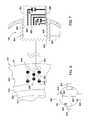
- FIG. 1is a cross-sectional schematic view of an exemplary etch processing chamber 100 having a pixilated substrate support assembly 126 .
- the pixilated substrate support assembly 126may be utilized in other processing chamber, for example plasma treatment chambers, annealing chambers, physical vapor deposition chambers, chemical vapor deposition chambers, and ion implantation chambers, among others, as well as other systems where the ability to control a temperature profile of a surface or workpiece, such as a substrate, is desirable.
- Independent and local control of the temperature across many discrete regions across a surfacebeneficially enables azimuthal tuning of the temperature profile, center to edge tuning of the temperature profile, and reduction of local temperature asperities, such as hot and cool spots.
- the processing chamber 100includes a grounded chamber body 102 .
- the chamber body 102includes walls 104 , a bottom 106 and a lid 108 which enclose an internal volume 124 .
- the pixilated substrate support assembly 126is disposed in the internal volume 124 and supports a substrate 134 thereon during processing.
- the walls 104 of the processing chamber 100include an opening (not shown) through which the substrate 134 may be robotically transferred into and out of the internal volume 124 .
- a pumping port 110is formed in one of the walls 104 or the bottom 106 of the chamber body 102 and is fluidly connected to a pumping system (not shown). The pumping system is utilized to maintain a vacuum environment within the internal volume 124 of the processing chamber 100 , while removing processing byproducts.
- a gas panel 112provides process and/or other gases to the internal volume 124 of the processing chamber 100 through one or more inlet ports 114 formed through at least one of the lid 108 or walls 104 of the chamber body 102 .
- the process gas provided by the gas panel 112are energized within the internal volume 124 to form a plasma 122 utilized to process the substrate 134 disposed on the pixilated substrate support assembly 126 .
- the process gasesmay be energized by RF power inductively coupled to the process gases from a plasma applicator 120 positioned outside the chamber body 102 .
- the plasma applicator 120is a pair of coaxial coils coupled through a matching circuit 118 to an RF power source 116 .
- a controller 148is coupled to the processing chamber 100 to control operation of the processing chamber 100 and processing of the substrate 134 .
- the controller 148may be one of any form of general-purpose data processing system that can be used in an industrial setting for controlling the various subprocessors and subcontrollers.
- the controller 148includes a central processing unit (CPU) 172 in communication with memory 174 and input/output (I/O) circuitry 176 , among other common components.
- CPUcentral processing unit
- I/Oinput/output
- Software commands executed by the CPU of the controller 148cause the processing chamber to, for example, introduce an etchant gas mixture (i.e., processing gas) into the internal volume 124 , form the plasma 122 from the processing gas by application of RF power from the plasma applicator 120 , and etch a layer of material on the substrate 134 .
- an etchant gas mixturei.e., processing gas
- the pixilated substrate support assembly 126generally includes at least a substrate support 132 .
- the substrate support 132may be a vacuum chuck, an electrostatic chuck, a susceptor, or other workpiece support surface. In the embodiment of FIG. 1 , the substrate support 132 is an electrostatic chuck and will be described hereinafter as the electrostatic chuck 132 .
- the pixilated substrate support assembly 126may additionally include a heater assembly 170 .
- the pixilated substrate support assembly 126may also include a cooling base 130 . The cooling base may alternately be separate from the pixilated substrate support assembly 126 .
- the pixilated substrate support assembly 126may be removably coupled to a support pedestal 125 .
- the support pedestal 125which may include a pedestal base 128 and a facility plate 180 , is mounted to the chamber body 102 .
- the pixilated substrate support assembly 126may be periodically removed from the support pedestal 125 to allow for refurbishment of one or more components of the pixilated substrate support assembly 126 .
- the facility plate 180is configured to accommodate a plurality of driving mechanism configured to raise and lower a plurality of lifting pins. Additionally, the facility plate 180 is configured to accommodate the plurality of fluid connections from the electrostatic chuck 132 and the cooling base 130 . The facility plate 180 is also configured to accommodate the plurality of electrical connections from the electrostatic chuck 132 and the heater assembly 170 . The myriad of connections may run externally or internally of the pixilated substrate support assembly 126 while the facility plate 180 provides an interface for the connections to a respective terminus.
- the electrostatic chuck 132has a mounting surface 131 and a workpiece surface 133 opposite the mounting surface 131 .
- the electrostatic chuck 132generally includes a chucking electrode 136 embedded in a dielectric body 150 .
- the chucking electrode 136may be configured as a mono polar or bipolar electrode, or other suitable arrangement.
- the chucking electrode 136is coupled through an RF filter 182 to a chucking power source 138 which provides a RF or DC power to electrostatically secure the substrate 134 to the upper surface of the dielectric body 150 .
- the RF filter 182prevents RF power utilized to form a plasma 122 within the processing chamber 100 from damaging electrical equipment or presenting an electrical hazard outside the chamber.
- the dielectric body 150may be fabricated from a ceramic material, such as AlN or Al 2 O 3 . Alternately, the dielectric body 150 may be fabricated from a polymer, such as polyimide, polyetheretherketone, polyaryletherketone and the like.
- the workpiece surface 133 of the electrostatic chuck 132may include gas passages (not shown) for providing backside heat transfer gas to the interstitial space defined between the substrate 134 and the workpiece surface 133 of the electrostatic chuck 132 .
- the electrostatic chuck 132may also include lift pin holes for accommodating lift pins (both not shown) for elevating the substrate 134 above the workpiece surface 133 of the electrostatic chuck 132 to facilitate robotic transfer into and out of the processing chamber 100 .
- the temperature controlled cooling base 130is coupled to a heat transfer fluid source 144 .
- the heat transfer fluid source 144provides a heat transfer fluid, such as a liquid, gas or combination thereof, which is circulated through one or more conduits 160 disposed in the base 130 .
- the fluid flowing through neighboring conduits 160may be isolated to enabling local control of the heat transfer between the electrostatic chuck 132 and different regions of the cooling base 130 , which assists in controlling the lateral temperature profile of the substrate 134 .
- a fluid distributormay be fluidly coupled between an outlet of the heat transfer fluid source 144 and the temperature controlled cooling base 130 .
- the fluid distributoroperates to control the amount of heat transfer fluid provided to the conduits 160 .
- the fluid distributormay be disposed outside of the processing chamber 100 , within the pixilated substrate support assembly 126 , within the pedestal base 128 or other suitable location.
- the heater assembly 170may include one or more main resistive heaters 154 and/or a plurality of pixel heaters 140 embedded in a body 152 .
- the main resistive heaters 154may be provided to elevate the temperature of the pixilated substrate support assembly 126 to a temperature for conducting chamber processes.
- the pixel heaters 140provide localized adjustments to the temperature profile of the pixilated substrate support assembly 126 generated by the main resistive heaters 154 .
- the main resistive heaters 154operate on a globalized macro scale while the pixel heaters operate on a localized micro scale.
- the main resistive heaters 154are coupled through an RF filter 184 to a main heater power source 156 .
- the power source 156may provide 500 watts or more power to the main resistive heaters 154 .
- the controller 148may control the operation of the main heater power source 156 , which is generally set to heat the substrate 134 to about predefined temperature.
- the main resistive heaters 154include a plurality of laterally separated heating zones, wherein the controller 148 enables one zone of the main resistive heaters 154 to be preferentially heated relative to the main resistive heaters 154 located in one or more of the other zones.
- the main resistive heaters 154may be arranged concentrically in a plurality of separated heating zones.
- the pixel heaters 140are coupled through an RF filter 186 to a pixel heater power source 142 .
- the pixel heater power source 142may provide 10 watts or less power to the pixel heaters 140 .
- the power supplied by the pixel heater power source 142is an order of magnitude less than the power supplied by the power source 156 of the main resistive heaters.
- the pixel heaters 140may additionally be coupled to a pixel controller 202 .
- the pixel controller 202may be located within or external to the substrate support assembly 126 .
- the pixel controller 202may manage the power provided from pixel heater power source 142 to individual or groups of pixel heaters 140 in order to control the heat generated locally at each pixel heaters 140 distributed laterally across the substrate support assembly 126 .
- An optical power source 178may coupled the pixel controller 202 to the controller 148 to decouple the controller 148 from influence of the RF energy with the processing chamber 100 .
- the one or more main resistive heaters 154 , and/or the pixel heaters 140may be formed in the electrostatic chuck 132 .
- the pixilated substrate support assembly 126may be formed without the heater assembly 170 and the electrostatic chuck 132 may be disposed directly on the cooling base 130 .
- the electrostatic chuck 132may include one or more thermocouples (not shown) for providing temperature feedback information to the controller 148 for controlling the power applied by the main heater power source 156 to the main resistive heaters 154 , for controlling the operations of the cooling base 130 , and controlling the power applied by the pixel heater power source 142 to the pixel heaters 140 .
- the temperature of the surface for the substrate 134 in the processing chamber 100may be influenced by the evacuation of the process gasses by the pump, the slit valve door, the plasma 122 and other factors.
- the cooling base 130 , the one or more main resistive heaters 154 , and the pixel heaters 140all help to control the surface temperature of the substrate 134 .
- main resistive heaters 154may be used to heat the substrate 134 to a temperature suitable for processing with a variation of about +/ ⁇ 10 degrees Celsius from one zone to another.
- main resistive heaters 154may be used to heat the substrate 134 to a temperature suitable for processing with a variation of about +/ ⁇ 1.5 degrees Celsius within a particular zone.
- Each zonemay vary from adjacent zones from about 0 degrees Celsius to about 20 degrees Celsius depending on process conditions and parameters. However, the requirement for minimizing variations in the critical dimensions across a substrate has reduced the acceptable variation in a determined process temperature of the surface of the substrate surface.
- a half a degree variation of the surface temperature for the substrate 134may result in as much as a nanometer difference in the formation of structures therein.
- the pixel heaters 140improve the temperature profile of the surface of the substrate 134 produced by the main resistive heaters 154 by reducing variations in the temperature profile to about +/ ⁇ 0.3 degrees Celsius.
- the temperature profilemay be made uniform or to precisely vary in a predetermined manner across regions of the substrate 134 through the use of the pixel heaters 140 to enable realization of desired results.
- FIG. 2is a partial cross-sectional schematic view illustrating portions of the pixilated substrate support assembly 126 . Included in FIG. 2 are portions of the electrostatic chuck 132 , the heater assembly 170 and the facility plate 180 .
- the body 152 of the heater assembly 170may be fabricated from a polymer such as a polyimide.
- the body 152may generally be cylindrical in plan form, but may also be formed in other geometrical shapes.
- the body 152has an upper surface 270 and a lower surface 272 .
- the upper surface 270faces the electrostatic chuck 132
- the lower surface 272faces the cooling base 130 .
- the body 152 of the heater assembly 170may be formed from two or more dielectric layers (shown in FIG. 2 as three dielectric layers 260 , 262 , 264 ) and heating the layers 260 , 262 , 264 under pressure to form a single body 152 .
- the body 152may be formed from polyimide layers 260 , 262 , 264 , which separate the main and pixel heaters 154 , 140 , which are heated under pressure to form the single body 152 of the heater assembly 170 .
- the pixel heaters 140may be placed in, on or between the first, second or third layers 260 , 262 , 264 prior to forming the body 152 .
- the main resistive heaters 154may be placed in, on or between on the first, second or third layers 260 , 262 , 264 prior to assembly, with at least one of the layers 260 , 262 , 264 separating and electrically insulating the heaters 154 , 140 . In this manner, the pixel heaters 140 and the main resistive heaters 154 become an integral part of the heater assembly 170 .
- FIGS. 4A-4Eare partial schematic views of the pixilated substrate support assembly 126 detailing various locations for the pixel heaters 140 and the main resistive heaters 154 , although not limiting to all embodiments.
- the pixilated substrate support assembly 126does not have a heater assembly ( 170 ) and the pixel heaters 140 and the main resistive heaters 154 are disposed in the electrostatic chuck 132 , for example, below the chucking electrode 136 .
- the pixel heaters 140are shown below the main resistive heaters 154 , the pixel heaters 140 may be alternatively positioned above the main resistive heaters 154 .
- the heater assembly 170 for the pixilated substrate support assembly 126includes the pixel heaters 140 while the main resistive heaters 154 are disposed in the electrostatic chuck 132 , for example, below the chucking electrode 136 .
- the pixel heaters 140may be disposed in the electrostatic chuck 132 while the main resistive heaters 154 are disposed in the heater assembly 170 .
- the heater assembly 170 for the pixilated substrate support assembly 126has the main resistive heaters 154 disposed therein.
- the pixel heaters 140are disposed in the electrostatic chuck 132 , for example, below the chucking electrode 136 .
- the heater assembly 170 for the pixilated substrate support assembly 126has pixel heaters 140 disposed therein while the main resistive heaters 154 are disposed on one of the heater assembly 170 or the electrostatic chuck 132 .
- the heater assembly 170isolates the pixel heaters 140 from the cooling plate 130 .
- the heater assembly 170 of the pixilated substrate support assembly 126has main resistive heaters 154 disposed therein.
- the pixel heaters 140are disposed in or on the heater assembly 170 , for example, below the electrostatic chuck 132 . It is contemplated that the pixel heaters 140 and the main resistive heaters 154 may be arranged in other orientations.
- the pixilated substrate support assembly 126may only have the plurality of pixel heaters 140 for heating the substrate 134 .
- the pixel heaters 140 and the main resistive heaters 154are disposed directly under each other within pixilated substrate support assembly 126 .
- the pixel heaters 140provide fine tune control for the temperature profile of the substrate 134 supported by the pixilated substrate support assembly 126 .
- the pixel heaters 140may be formed or disposed on or in the body 152 of the heater assembly 170 or electrostatic chuck 132 .
- the pixel heaters 140may be formed by plating, ink jet printing, screen printing, physical vapor deposition, stamping, wire mesh or other suitable manner. In this manner fabrication of the pixilated substrate support assembly 126 is simplified.
- the pixel heaters 140are disposed within the heater assembly 170 while forming the heater assembly 170 .
- the pixel heaters 140are directly disposed on the mounting surface 131 of the electrostatic chuck 132 .
- the pixel heaters 140may be in a sheet form which can be adhered to the mounting surface 131 of the electrostatic chuck 132 , or the pixel heaters may be deposited by other means.
- the pixel heaters 140can be deposited on the mounting surface 131 by physical vapor deposition, chemical vapor deposition, screen printing or other suitable methods.
- the main resistive heaters 154can be in the electrostatic chuck 132 or heating assembly 170 as shown above.
- the main resistive heaters 154may be formed or disposed on or in the body 152 of the heater assembly 170 or electrostatic chuck 132 .
- the main resistive heaters 154may be formed by plating, ink jet printing, screen printing, physical vapor deposition, stamping, wire mesh or other suitable manner. In this manner fabrication of the pixilated substrate support assembly 126 is simplified.
- main resistive heaters 154are disposed within the heater assembly 170 while forming the heater assembly 170 .
- main resistive heaters 154are directly disposed on the mounting surface 131 of the electrostatic chuck 132 .
- main resistive heaters 154may be in a sheet form which can be adhered to the mounting surface 131 of the electrostatic chuck 132 , or main resistive heaters 154 may be deposited by other means.
- main resistive heaters 154can be deposited on the mounting surface 131 by physical vapor deposition, chemical vapor deposition, screen printing or other suitable methods.
- the pixel heaters 140can be in the electrostatic chuck 132 or heating assembly 170 as shown above.
- the main resistive heaters 154may be fabricated similar to the pixel heaters 140 , and in such embodiments, may optionally be utilized without benefit of additional pixel heaters 140 .
- the main resistive heaters 154 of the pixilated substrate support assembly 126are pixilated, that is, segmented in to a plurality of discreet resistive heating elements. Segmenting the main resistive heaters 154 in the form of small resistive heaters allows local control of hot and cold spots on the surface of the substrate 134 .
- An additional layer of pixel heaters 140is optional, depending on the desired level of temperature control.
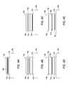
- FIG. 7is a graphical depiction for a wiring layout for a segmented main resistive heaters 154 formed from a plurality of unit heaters 846 .
- the unit heaters 846may be controlled through use of the pixel controller 202 as described above, or through the use of a pixel heater controller in the form of a hardware wiring key 802 as depicted in FIG. 7 .
- One implementation for using hardware wiring keys 802is illustrated in a top plan view of the facility plate 180 shown in FIG. 8 .
- the pixilated substrate support assembly 126may have one or more main resistive heater 154 , illustratively shown as four main resistive heaters 154 , each defining one of four zones 810 , 820 , 830 , 840 .
- the temperature in each zone 810 , 820 , 830 , 840may be independently controlled by the main resistive heater 154 associated with zone.
- each main resistive heaters 154is comprised of a plurality of separated unit heaters 846 .
- the unit heaters 846may be either active (active unit heaters 842 ) or inactive (inactive unit heaters 844 ).
- Active unit heaters 842are coupled to a power source and contribute heat to the main resistive heaters 154 .
- the inactive unit heaters 844are a power source and thus, do not contribute heat to the main resistive heaters 154 .
- the temperature profile of the substrate support assembly 126may be controlled, for example, to control local hot or cold spots, to provide center to edge tuning of the temperature profile, and to provide azimuthal tuning of the lateral temperature profile of the pixilated substrate support assembly 126 , and consequently, the substrate 134 processed thereon.
- the unit heaters 846 for each main resistive heater 154may be selected to form a pattern of active heater density within each of the zones 810 , 820 , 830 , 840 .
- the pattern of the unit heaters 846may be tightly packed and uniform, similar to the pattern of unit heaters labeled 854 . Alternately, the pattern for the unit heaters 846 may be loosely spaced.
- the unit heaters 846may be switched between active unit heaters 842 and inactive unit heaters 844 using hardware, such as the hardware wiring key 802 , the pixel controller 202 , software or firmware executed by controller 148 , or through another method or device.
- the temperature profile generated from the main resistive heaters 154 in each of the zones 810 , 820 , 830 , 840may be refined by selectively activating the unit heaters 846 to control the heat supplied by the main resistive heaters 154 .
- Each unit heater 846that is all active unit heaters 842 and all inactive unit heaters 844 , has a wired connection 860 .
- the wired connections 860are routed to a receptacle 804 , for example, formed in the facility plate 180 .
- the wired connections 860may extend outward of the pixilated substrate support assembly 126 and run down the outside of the pixilated substrate support assembly 126 to the receptacle 804 in the facility plate 180 .
- the wired connection 860may run internally through the heater assembly 170 , for example, through a hole in the cooling base 130 to the receptacle 804 in facility plate 180 .
- the receptacle 804 in the facility plate 180has an interior surface 805 and a side surface 806 .
- the wired connections 860may terminate at the interior surface 805 , thus forming a connector or socket.
- a control board connection 868may terminate at the side surface 806 with a connector or socket.
- the control board connection 868may be a single power lead or a plurality of power leads.
- the wired connections 860 and the control board connections 868are part of a circuit. Alternately, the wired connections 860 and the control board connections 868 may both residing on the same surface of the facility plate 180 . For example, both the wired connections 860 and the control board connections 868 may reside on an interior surface 805 of the receptacle 804 .
- a gap in the circuitis formed at the receptacle 804 such that no current may flow across the circuit, i.e. from the control board connections 868 to the wired connections 860 .
- the hardware wiring key 802is configured to fit in the receptacle 804 .
- the hardware wiring key 802may be flush with outer surface 880 of the facility plate 180 while a front surface 885 of the hardware wiring key 802 makes contact with the interior surface 805 of the receptacle 804 .
- the side surface 886 of the hardware wiring key 802is in contact the side surface 806 of the receptacle.
- the hardware wiring key 802is configured to selectively fill the gap in the circuit at the receptacle 804 such that current may flow from the control board connections 868 to selected wired connections 860 . In this manner the electrical connections between the wired connections 860 and the control board connections 868 can be made.
- the hardware wiring key 802is configured to selectively provide power to the unit heaters 846 .
- the hardware wiring key 802may use a common negative terminal for each of the wired connections 860 .
- all the negative terminalsmay utilize a common bus that may be formed in the jacket of the hardware wiring key 802 or the negative terminal may be a shared pin connection.
- the hardware wiring key 802may use individual negative terminal for each of the wired connections 860 .
- the negative terminalmay have a gate switch or other means for selectively interrupting the flow of current across the terminal.
- the hardware wiring key 802may be formed in a manner to preselect only those circuits which are desired to make active are available to deliver power to the unit heaters 846 .
- the inactive circuitsmay have gaps or gates 864 , unformed circuitry within the hardware wiring key 802 , or an insulating cap (not shown), among other suitable means for interrupting the flow of power to the wired connections 860 of the unit heaters 846 within the main resistive heaters 154 .
- one hardware wiring key 802may be utilized to provide a predefined lateral temperature distribution of the substrate while performing one process, and replaced by a hardware wiring key 802 having a different preselection of circuits which are desired to make active are available to deliver power to the unit heaters 846 which will yield a different predefined lateral temperature distribution of the substrate while performing another process.
- different hardware wiring keys 802may be efficiently swapped out to provide different temperature profiles, and accordingly, greater flexibility in ensuring realization of beneficial processing results.
- the wired connections 860may be divided and equally spaced about the outer surface 880 of the facility plate 180 .
- the facility platehas four receptacles 804 , each receptacle having a substantially equal number of wired connections 860 .
- This arrangementallows the pixilated substrate support assembly 126 to be symmetrically balanced and minimizes the effects of the wiring on processes occurring within the processing chamber 100 .
- the arrangement of unit heaters 846 and connectionsprovide a homogenous construction for the pixilated substrate support assembly 126 , and promotes process symmetry.
- the unit heaters 846of the main resistive heaters 154 , allow the main resistive heaters 154 to have a temperature range between about ambient to about 500 degrees Celsius with the ability to control the lateral temperature profiled in increments of about 0.3 degrees Celsius.
- the pixilated substrate support assembly 126having main resistive heaters 154 configured with unit heaters 846 , has demonstrated the ability to control the temperature uniformity of a substrate processed thereon to less than about ⁇ 1.5 degrees Celsius.
- the heater assembly 170may be coupled to the mounting surface 131 of the electrostatic chuck 132 utilizing a bonding agent 244 .
- the bonding agent 244may be an adhesive, such as an acrylic-based adhesive, an epoxy, a silicon based adhesive, a neoprene-based adhesive or other suitable adhesive.
- the bonding agent 244is an epoxy.
- the bonding agent 244may have a coefficient of thermal conductivity selected in a range from 0.01 to 200 W/mK and, in one exemplary embodiment, in a range from 0.1 to 10 W/mK.
- the adhesive materials comprising the bonding agent 244may additionally include at least one thermally conductive ceramic filler, e.g., aluminum oxide (Al 2 O 3 ), aluminum nitride (AlN), and titanium diboride (TiB 2 ), and the like.
- at least one thermally conductive ceramic fillere.g., aluminum oxide (Al 2 O 3 ), aluminum nitride (AlN), and titanium diboride (TiB 2 ), and the like.
- the heater assembly 170is coupled to the cooling base 130 utilizing a bonding agent 242 .
- the bonding agent 242may be similar to the bonding agent 244 and may be an adhesive, such as an acrylic-based adhesive, an epoxy, a neoprene-based adhesive or other suitable adhesive.
- the bonding agent 242is an epoxy.
- the bonding agent 242may have a coefficient of thermal conductivity selected in a range from 0.01 to 200 W/mK and, in one exemplary embodiment, in a range from 0.1 to 10 W/mK.
- the adhesive materials comprising the bonding agent 242may additionally include at least one thermally conductive ceramic filler, e.g., aluminum oxide (Al 2 O 3 ), aluminum nitride (AlN), and titanium diboride (TiB 2 ), and the like.
- at least one thermally conductive ceramic fillere.g., aluminum oxide (Al 2 O 3 ), aluminum nitride (AlN), and titanium diboride (TiB 2 ), and the like.
- the bonding agents 244 , 242may be removed when refurbishing one or both of the electrostatic chuck 132 , the cooling base 130 and the heater assembly 170 .
- the heater assembly 170is removably coupled to the electrostatic chuck 132 and to the cooling base 130 utilizing fasteners or clamps (not shown).
- the heater assembly 170includes a plurality of pixel heaters 140 , illustratively shown as pixel heaters 140 a , 140 b , 140 c .
- the pixel heaters 140are generally an enclosed volume within the heater assembly 170 in which a plurality of resistive heaters effectuate heat transfer between the heater assembly 170 and electrostatic chuck 132 .
- Each pixel heater 140may be laterally arranged across the heater assembly 170 , and thus defined a cell 200 within the heater assembly 170 for locally providing additional heat to region of the heater assembly 170 (and portion of the main resistive heater 154 ) aligned that cell 200 .
- the number of pixel heaters 140 formed in the heater assembly 170may vary, and it is contemplated that there is at least an order of magnitude more pixel heaters 140 (and cells 200 ) greater than the number of the main resistive heaters 154 . In one embodiment in which the heater assembly 170 has four main resistive heaters 154 , there may be greater than 40 pixel heaters 140 . However, it is contemplated that there may be about 200, about 400 or even more pixel heaters 140 in a given embodiment of a substrate support assembly 126 configured for use with a 300 mm substrate. Exemplary distribution of the pixel heaters 140 are described further below with reference to FIGS. 3A-3D .
- the cells 200may be formed through one or more layers 260 , 262 , 264 comprising the body 152 of the heater assembly 170 . In one embodiment, the cells are open to the lower and upper surface 272 , 272 of the body 152 .
- the cellsmay include sidewalls 214 .
- the sidewalls 214may be comprised of a material (or gap) acting as a thermal choke 216 .
- the thermal chokes 216are formed in the upper surface 270 of the body 152 . The thermal chokes 216 separate and reduce conduction between adjacent cells 200 .
- An additional thermal choke 216may be formed between the radially outermost cells 200 and a laterally outermost sidewall 280 of the body 152 .
- This outermost thermal choke 216 located between the cells 200 and the laterally outermost sidewall 280 of the body 152minimizes heat transfer between the cells 200 , adjacent to the laterally outermost sidewall 280 , and the internal volume 124 of the processing chamber 100 . Thereby allowing more precise temperature control closer to the edge of the pixilated substrate support assembly 126 , and as a result, better temperature control to the outside diameter edge of the substrate 134 .
- each pixel heater 140may be independently coupled a pixel controller 202 .
- the pixel controller 202may be disposed in the pixilated substrate support assembly 126 .
- the pixel controller 202may regulate the temperature of the pixel heaters 140 in the heater assembly 170 at each cell 200 relative to the other cells 200 , or alternatively, regulate the temperature of a group of pixel heaters 140 in the heater assembly 170 across a group of cells 200 relative to the another group of cells 200 .
- the pixel controller 202may toggle the on/off state or control the duty cycle for individual or groups of the pixel heaters 140 .
- the pixel controller 202may control the amount of power delivered to the individual or groups of pixel heaters 140 .
- the pixel controller 202may provide one or more pixel heaters 140 ten watts of power, other pixel heaters 140 nine watts of power, and still other pixel heaters one watt of power.
- each cell 200may be thermally isolated from the neighboring cells 200 , for example, using a thermal choke 216 , which enables more precise temperature control.
- each cell 200may be thermally joined to an adjacent cell creating an analogue (i.e., smooth or blended) temperature profile along an upper surface 270 of the heater assembly 170 .
- a metal layersuch as aluminum foil, may be used as a thermal spreader between the main resistive heaters 154 and the pixel heaters 140 .
- the use of independently controllable the pixel heaters 140 to smooth out or correct the temperature profile generated by the main resistive heaters 154enable control of the local temperature uniformity across the substrate to very small tolerances, thereby enabling precise process and CD control when processing the substrate 134 . Additionally, the small size and high density of the pixel heaters 140 relative to the main resistive heaters 154 enables temperature control at specific locations of the pixilated substrate support assembly 126 , substantially without affecting the temperature of neighboring areas, thereby allowing local hot and cool spots to be compensated for without introducing skewing or other temperature asymmetries.
- the pixilated substrate support assembly 126having a plurality of pixel heaters 140 , has demonstrated the ability to control the temperature uniformity of a substrate 134 processed thereon to less than about ⁇ 0.3 degrees Celsius.
- the pixel controller 202may include an electrical power circuit 210 and an optical control circuit 220 .
- the electrical power circuit 210is coupled to the pixel heaters 140 .
- Each pixel heater 140has a pair of power leads (connectors 250 ) which are connected to the electrical power circuit 210 .
- 50 pairs of power leads (connectors 250 )are needed for controlling the pixel heaters 140 .
- the RF energy supplied into the processing chamber 100 for forming the plasmacouples to the power leads. Filters, such as the RF filters 182 , 184 , 186 shown in FIG.
- each heaterrequires a dedicated RF filter. Accordingly, as the space for dedicated RF filters very limited, the number of heaters utilized within the substrate support assembly is also limited, thereby limiting the number of main heater zones which may be employed, and making pixilated corrective heaters impossible to implement.
- the use of the electrical power circuit 210 with the optical control circuit 220allow more heaters, and consequently, superior lateral temperature control.
- a flex circuit 600may be utilized to assist controlling the plurality of pixel heaters 140 .
- the flex circuit 600may form a matrix pattern with the pixel heaters 140 .
- the flex circuit 600may consist of a number non-intersecting positive leads 640 and negative leads 650 , each attached at one end to the pixel controller 202 .
- Each positive lead 640may have a plurality of pixel heater assemblies 662 bridging a connection to a corresponding negative lead 650 .
- the pixel heater assembly 662is deposed between each connection of the positive and negative leads 640 , 650 .
- the flex circuit 600may have 9 positive leads 640 and 9 negative leads 650 and therefore as many as 81 pixel heater assemblies 662 .
- the pixel heater assembly 662has a pixel heater 663 and a diode 664 connected in series.
- the pixel heater 663attaches to the positive lead 640 and the diode 664 may attach to the negative lead 650 .
- pixel heater 663attaches to the negative lead 650 and the diode 630 may attach to the positive lead 640 .
- the diode 664ensures current flows only in one direction. In one embodiment, the direction of the current flow for each of the pixel heater assemblies 662 is from the positive lead 640 to the negative lead 650 .
- the pixel controller 202may open and/or close individual circuits to provide a predetermined current flow across a selection of the positive leads 640 and the negative leads 650 .
- the pixel controller 202may provide for current flow on positive lead labeled 641 and a return flow for the current on negative lead labeled 653 , with all other positive and negative leads 640 , 650 acting as open circuits.
- the pixel controller 202may selectively provide for current flow on positive leads labeled 642 and 643 while providing for a return flow on a negative lead 652 , with all other positive and negative leads 640 , 650 acting as open circuits.
- the pixel controller 202may therefore selectively provide current to the pixel heater assemblies 662 disposed between the selected combinations of positive and negative leads 640 , 650 .
- the flex circuit 600completes individual circuits with the fewest number of connections back to the pixel controller 202 for supplying power to each pixel heater 663 .
- the pixel controller 202provides current on the positive lead labeled 641 and a return path for the current is provided on all the negative leads 650 .
- Pixel heaters 140 along the top row 612are selectively turned on (active) while the remaining of the pixel heaters 140 are inactive.
- the pixel controller 202provides current on the positive leads labeled 641 and 642 and provides a return path for the current on the negative leads labeled 651 and 652 .
- a small group of four pixel heaters 691 , 692 , 693 , 694are selectively turned on while the remaining pixel heaters 140 remain inactive (i.e., unpowered).
- the pixel controller 202may be utilized to selectively activate various pixel heaters 140 by activating selected the positive leads 640 and selected the negative leads 650 .
- the pixel controller 202may also control the voltage across or current through a given pixel heater to control the amount of heat generated by a particular pixel heater.
- the pixel controller 202may alternatively, or in addition, control the duty cycle for a given pixel heater to control the amount of heat generated by a particular pixel heater over time.
- the pixel controller 202may alternatively, or in addition, scan through the pixel heaters to control the amount of heat generated by a particular pixel heater over time.
- the flex circuit 600may be formed in, on, or below, one of the layers 260 , 262 , 264 comprising the body 152 of the heater assembly 170 .
- the pixel heaters 140may be disposed above or in conjunction with the flex circuit 600 .
- the flex circuit 600may be deposited, plated, ink jet printed, screen printed or formed in any suitable manner.
- the positive leads 640 and the negative leads 650may form one or more connectors 250 to connect the flex circuit 600 to the pixel controller 202 .
- the connectors 250may extend internally through the pixilated substrate support assembly 126 .
- the cooling base 130 and the facility plate 180may have one or more passages formed therethrough to accommodate the passage of the connectors 250 .
- the connectors 250may be divided, positioned or distributed throughout the pixilated substrate support assembly 126 in such a manner that balances any effects of the wiring on the plasma processes ongoing in the processing chamber 100 .
- four connectors 250may pass through four equally spaced passages formed about a center of the pixilated substrate support assembly 126 .
- the flex circuit 600may be printed on or within the layers of the heater assembly 170 with a hundred or more terminal leads for operating 50 or more pixel heaters 140 .
- four hundred terminal leadsare utilized to provide power to two hundred pixel heaters 140 .
- the terminal leadsmay be divided into separate flexible strips, such as a ribbon cable or circuit, which may be run through slots formed in the cooling plate 130 .
- the flexible strips containing the terminal leadby run through equally spaced slots formed through the cooling plate 130 to the facility plate 180 to provide symmetrical geometry which contributes to symmetrical temperature control and process uniformity.
- the electrical power circuit 210may switch or cycle power to the plurality of connectors 250 coming from the flex circuit 600 .
- the electrical power circuit 210provides power to each of the connectors 250 to activate one or more pixel heaters 140 .
- the electrical power sourceultimately supplies power to the plurality of pixel heaters 140
- the electrical power circuit 210has a single power source, i.e. the pixel heater power source 142 , and thus only requires only the single filter 184 .
- the space and expense for additionally filtersare mitigated, while enabling use of many heaters and heater zones.
- the optical control circuit 220may be coupled to the electrical power circuit 210 by an optical cable 226 , such as a fiber optic cable, to control the power supplied to the connectors 250 and thus, the pixels heaters 140 .
- the optical control circuit 220may be coupled to an optical power source 178 through an optical wave guide 228 .
- the optical power source 178is coupled to the controller 148 for providing signals controlling the function of the pixel heaters 140 .
- the optical cable 226 and optical wave guide 228are not subject to electromagnetic interference or radio frequency (RF) energy. Thus, an RF filter to protect the optical power source 178 from RF energy in the pixel controller 202 is unnecessary, thereby allowing more space in the substrate support assembly 126 for routing other utilities.
- RFradio frequency
- the optical control circuit 220may send commands, or instruction, to the electrical power circuit 210 for regulating each pixel heater 140 or groups/regions of pixel heaters 140 . As seen in the flex circuit 600 of FIG. 6 , a single pixel heater 140 or groups/regions of pixel heaters 140 may be activated using a minimum number of connections back to the electrical power circuit 210 and controlled by the optical control circuit 220 .
- the optical control circuit 220may be programmed and calibrated by measuring the temperature rise at each pixel heater 140 .
- the temperature risemay be associated with incremental power increases to the pixel heaters 140 .
- the temperature risemay be associated with a percentage increase, for example 5% increase, in the power supplied to the pixel heater 140 .
- a temperature mapmay be obtained using this method.
- the mapmay correlate the CD or temperature to the power distribution curve for each pixel heater 140 .
- the pixel heater 140may be used to generate a temperature profile on the substrate based on a program regulating power settings for the individual pixel heaters 140 .
- the logiccan be placed directly in the optical control circuit 220 or in an externally connected controller, such as the controller 148 .
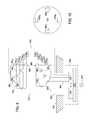
- FIG. 3Ais a cross-sectional view of FIG. 2 along a section line A-A, according to one embodiment.
- FIGS. 3B-3Dare cross-sectional views along the same section line A-A of FIG. 2 , according to alternate embodiments.
- the plurality of pixel heaters 140are disposed along the plane of the cross section line A-A through the body 152 of the heater assembly 170 .
- the thermal choke 216is disposed between each neighboring cell 200 , each cell 200 associated with at least one of the of pixel heaters 140 . Additionally, the thermal choke 216 is disposed along an outer surface 326 of the pixilated substrate support assembly 126 .
- the number of cells 200 shownare for illustration only, and any number of embodiments may have substantially more (or less) cells 200 .
- the number of pixel heaters 140may be at least an order of magnitude greater than the number of main resistive heaters 154 .
- the number of pixel heaters 140 located across the pixilated substrate support assembly 126may easily be in excess of several hundred.
- Each pixel heater 140has a resistor 304 ending in terminals 306 , 308 . As current enters one terminal, such as the terminal labeled 306 , and exists the other terminal, such as the terminal labeled 308 , the current travels across the wire of the resistor 304 and generates heat.
- the pixel heater 140may have a design power density to provide the appropriate temperature rise along the outer surface 326 of the pixilated substrate support assembly 126 .
- the amount of heat released by the resistor 304is proportional to the square of the current passing therethrough.
- the power design densitymay be between about 1 watt/cell to about 100 watt/cell, such as 10 watt/cell.
- the resistor 304may be formed from a film of nichrome, rhenium, tungsten, platinum, tantalum or other suitable materials.
- the resistor 304may have an electrical resistivity ( ⁇ ).
- a low ⁇indicates a material that readily allows the movement of an electric charge across the resistor 304 .
- Platinumhas a ⁇ of about 1.06 ⁇ 10 ⁇ 7 ( ⁇ m) at 20° C.
- Tungstenhas a ⁇ of about 5.60 ⁇ 10 ⁇ 8 ( ⁇ m) at 20° C.
- Nichromehas a ⁇ of about 1.1 ⁇ 10 ⁇ 8 to about 1.5 ⁇ 10 ⁇ 8 ( ⁇ m) at 20° C.
- the resistor 304 comprised of nichromeallows the electrical charge to move more readily, and thus, generate more heat.
- the electrical properties for tungstenmay differentiate the material as a resistive heater in certain temperature ranges.
- the resistor 304may have a film thickness (not shown) and a wire thickness 372 configured to efficiently provide heat when a current is passed along the resistor 304 .
- An increase in the wire thickness 372 for the resistor 304may result in a decrease in the resistance R of the resistor 304 .
- the wire thickness 372may range from about 0.05 mm to about 0.5 mm for a tungsten wire and about 0.5 mm to about 1 mm for a nichrome wire.
- a resistor 304is comprised of tungsten having a wire thickness 372 of about 0.08 mm and a resistance of about 50 Ohms at 10 watts of power.
- the pixel heaters 140may be configured in a pattern 390 to efficiently generate a heat profile along the surface of the pixilated substrate support assembly 126 .
- the pattern 390may be symmetric about a midpoint 392 while providing clearance in and around holes 322 for lift pins or other mechanical, fluid or electrical connections.
- Each pixel heater 140may be controlled by the pixel controller 202 .
- the pixel controller 202may turn on a single pixel heater 140 defining a heater 340 ; or a plurality of pixel heaters 140 grouped to define an inner wedge 362 , a perimeter group 364 , a pie shaped area 360 , or other desired geometric configuration, including non-contiguous configurations.
- temperaturecan be precisely controlled at independent locations along the surface of the pixilated substrate support assembly 126 , such independent locations not limited to concentric ring such as known in the art.
- the pattern shownis comprised of smaller units, the pattern may alternatively have larger and/or smaller units, extend to the edge, or have other forms.
- FIG. 3Bis a top view of the plurality of pixel heaters 140 disposed along the plane of the cross section line AA through the body 152 , according to another embodiment.
- the thermal chokes 216may optionally be present.
- the pixel heaters 140are arranged in the form of a grid, thus defining an array of temperature control cells 200 also arranged in the grid pattern.
- the grid pattern of pixel heaters 140is shown as an X/Y grid comprised of rows and columns, the grid pattern of pixel heaters 140 may alternatively have some other uniformly packed form, such as a hexagon close pack. It should be appreciated, as discussed supra, the pixel heaters 140 may be activated in groups or singularly.
- FIG. 3Cis a top view of the plurality of pixel heaters 140 disposed along the plane of the cross section line AA through the body 152 , according to another embodiment.
- FIG. 3Cillustrates a plurality of pixel heaters 140 arranged in a polar array in the body 152 .
- one or more of thermal chokes 216may be disposed between the pixel heaters 140 .
- the polar array pattern of the pixel heaters 140defines the neighboring cells 200 , which are thus also be arranged in a polar array.
- thermal chokes 216may be utilized to isolate adjacent cells 200 from neighboring cells 200 .
- FIG. 3Dis a top view of the plurality of pixel heaters 140 disposed along the plane of the cross section line A-A through the body 152 , according to another embodiment.
- FIG. 3Dillustrates a plurality of pixel heaters 140 arranged in the body 152 in concentric channels.
- the concentric channel pattern of the pixel heaters 140may be optionally separated by thermal chokes 216 . It is contemplated that the pixel heaters 140 and cells 200 may be arranged in other orientations.
- FIG. 9a graphical depiction is provided for an alternate wiring schema for the main resistive heaters 154 and the pixel heaters 140 .
- the wiring schemadoes not make use of the hardware key ( 802 in FIG. 7 ).
- the main resistive heaters 154 and the pixel heaters 140may be attached to a controller 902 .
- the controller 902is attached to a power source 978 through a common filter 910 .
- Controller 902is similar to controller 202 shown in FIGS. 1 and 2 and has a similar version of the electrical controller 210 and the optical controller 220 .
- pixel heater 140 1may represent a large group of pixel heaters in a common zone, or alternatively, to all the pixel heaters 140 disposed across the pixilated substrate support assembly 126 .
- the electrical controller 210accepts a plurality of power ribbons 912 , 922 from both the pixel heaters 140 and the main resistive heaters 154 through a hole or slot 920 formed through the cooling base 130 .
- the ribbons 912 , 922graphically depict a number of power leads for each pixel heater 140 and main resistive heater 154 .
- power ribbon 912comprises separate power leads for the pixel heaters 140 (1-n) .
- each power leadhas a switch 960 which may be activated by a respective control lead. It is contemplated that a single ribbon, or even three or more ribbons, may be utilized to route the power leads for the pixel heaters 140 and main resistive heater 154 .
- the optical controller 220accepts a plurality of control ribbons 940 , 950 from both the pixel heaters 140 and the main resistive heaters 154 through the slot 920 formed through the cooling base 130 .
- the ribbons 940 , 950graphically depict a number of control leads for each pixel heater 140 and main resistive heater 154 .
- control ribbon 940comprises separate control leads.
- the optical controller 220may take input, from a program, temperature measuring device, an external controller, a user or by other source, and determines which pixel heaters 140 and main resistive heaters 154 to energize.
- the optical controller 220uses optics to transmit between the input device, the switches and electrical controller, the optical controller is not subject to RF interference and does not propagate the same to regions outside of the processing chamber. It is contemplated that a single ribbon, or even three or more ribbons, may be utilized to route the control leads.
- the control leads 940provide signals generated by the optical controller 220 to control the state of a switch 960 .
- the switch 960may be a field effect transistor, or other suitable electronic switch. Alternately, the switch 960 may be embedded in an optically controlled circuit board in the electrical controller 210 .
- the switch 960may provide simple cycling for the heaters 154 , 140 between an energized (active) state and a de-energized (inactive) state. Alternately, the switch may be a variable resistor, or other suitable device, which can control the amount of power supplied to the heaters 154 , 140 .
- the controller 202provides a signal along the control ribbon 940 1 to instruct the switch 960 1 to allow 50% of the power to pass therethrough.
- the power controller 210provides about 10 watts of power along the power ribbon 912 1 .
- the switch 960 1allows 50% of the supplied power to pass through to a pixel heater 140 1 which heats up with about 5 watts of power.
- the controller 202provides a signal along the control ribbon 950 2 to instruct the switch 960 2 to allow 100% of the power to pass therethrough.
- the power controller 210provides about 100 watts of power along the power ribbon 922 2 .
- the switch 960 2allows 100% of the supplied power to pass through to the main resistive heater 154 2 which heats up with about 100 watts of power.
- the main resistive heaters 154 (1-N)may all be operated from controller 202 .
- the pixel controller 202provides a signal along the control ribbon 940 to instruct the switches 960 to be in either an active state that allows power to pass therethrough or an inactive state that prevents power from passing therethrough.
- the power controller 210provides about 10 watts of power along the power ribbon 912 to each pixel heater 140 coupled to a switch 960 in the active state.
- the pixel controller 202independently controls at least one of the duration that the switch 960 remains in the active state and the duty cycle of each of the switch 960 relative to the other switches 960 , which ultimately provides controls the temperature uniformity of the pixilated substrate support assembly 126 and substrate positioned thereon.
- the switches 960 controlling power to the main resistive heaters 154may be similarly controlled.
- each main resistive heater 154 (1-N)may have a separate controller 202 .
- the pixel heaters (1-N) common to a zone with one main resistive heater 154 (1-N)may share the controller 202 with the common main resistive heater 154 (1-N) .
- FIG. 10is a top plan view of the cooling base 130 having holes 960 configured for the wiring schema of four zones and four equally spaced controllers 202 .
- separate controllers 202may be utilized to split up the number of pixel heaters 140 serviced by a single controller. Splitting up the control of the pixel heaters 140 allows for smaller controllers and less space required to route the ribbons through the slots 920 formed through the cooling base, as shown in FIG. 9 .
- the number and density of the pixel heaters 140contribute to the ability for controlling the temperature uniformity across the substrate to very small tolerances which enables precise process and CD control when processing the substrate 134 . Additionally, individual control of one pixel heaters 140 relative to another pixel heaters 140 enables temperature control at specific locations in the pixilated substrate support assembly 126 without substantially affecting the temperature of neighboring areas, thereby allowing local hot and cool spots to be compensated for without introducing skewing or other temperature asymmetries.
- the pixel heaters 140may have an individual temperature range between about 0.0 degrees Celsius and about 10.0 degrees Celsius with the ability to control the temperature rise in increments of about 0.1 degrees Celsius.
- the plurality of pixel heaters 140 in the pixilated substrate support assembly 126 in conjunction with the main resistive heaters 154have demonstrated the ability to control the temperature uniformity of a substrate 134 processed thereon to less than about ⁇ 0.3 degrees Celsius.
- the pixel heaters 140allow both lateral and azimuthal tuning of the lateral temperature profile of the substrate 134 processed on the pixilated substrate support assembly 126 .
- FIG. 5is a flow diagram for one embodiment of a method 500 for processing a substrate utilizing a pixilated substrate support assembly, such as the pixilated substrate support assembly described above, among others.
- the method 500begins at block 502 by applying power to a main resistive heater formed in a pixilated substrate support assembly.
- the main resistive heatermay be a single heater, or segmented into zones.
- the main resistive heater zonesmay be independently controllable.
- poweris provided to a plurality of pixel heaters distributed laterally within the pixilated substrate support assembly. At least two of the pixel heaters generating a predetermined different amount of heat. The difference in heat generated by one pixel heater relative another may be controlled by controlling at least one or more of the duty cycle, voltage, current, duration of power applied to one pixel heater relative another. The power may also be sequentially scanned across pixel heaters.
- Control of the power provided to the pixel heatersmay be provide through an optical signal interfacing with a controller disposed in the pixilated substrate support assembly.
- a workpiecesuch as a substrate
- the substratemay be processed in a vacuum chamber, for example using a plasma process.
- the vacuum processwhich may be optionally performed in the presence of a plasma within the processing chamber, may be one of etching, chemical vapor deposition, physical vapor deposition, ion implantation, plasma treating, annealing, oxide removal, abatement or other plasma process. It is contemplated that the workpiece may be processed on the temperature controlled surface in other environments, for example, at atmospheric conditions, for other applications.
- power provided to the plurality of pixel heaters distributed laterally within the pixilated substrate support assemblymay be changed in response to process conditions or a change in a process recipe.
- the power provided to the plurality of pixel heatersmay be changed utilizing commands from the pixel controller 202 , or changing one hardware wiring key 802 to a different hardware wiring key 802 .
- a processing chambercomprising:
- a pixilated substrate support assemblycomprising:
- a plurality of pixel heatersin column with the main resistive heaters and disposed in the pixilated substrate support, wherein a quantity of the pixel heaters is an order of magnitude greater than a quantity of the main resistive heaters and the pixel heaters are independently controllable relative to each other as well as the main resistive heaters.
- a pixel heater controller for regulating a temperature output for each pixel heateris coupled to the cooling plate.
- a substrate support assemblycomprising:
- a substrate supporthaving a substrate support surface and a lower surface
- a pixel heater controllercoupled each group of resistive heaters, the pixel heater controller operable to control which resistive heater within a given zone generates more heat than other resistive heaters within the given zone.
Landscapes
- Engineering & Computer Science (AREA)
- Microelectronics & Electronic Packaging (AREA)
- Condensed Matter Physics & Semiconductors (AREA)
- General Physics & Mathematics (AREA)
- Manufacturing & Machinery (AREA)
- Computer Hardware Design (AREA)
- Physics & Mathematics (AREA)
- Power Engineering (AREA)
- Container, Conveyance, Adherence, Positioning, Of Wafer (AREA)
- Drying Of Semiconductors (AREA)
- Resistance Heating (AREA)
- Control Of Resistance Heating (AREA)
- Physical Vapour Deposition (AREA)
- Chemical Vapour Deposition (AREA)
Abstract
Description
- This application claims benefit of U.S. Provisional Application Ser. No. 61/937,348, filed Feb. 7, 2014 (Attorney Docket No. APPM/21606USL), of which is incorporated by reference in its entirety.
- 1. Field
- Implementations described herein generally relate to semiconductor manufacturing and more particularly to temperature controlled substrate support assembly and method of using the same.
- 2. Description of the Related Art
- As the feature size of the device patterns get smaller, the critical dimension (CD) requirements of these features become a more important criterion for stable and repeatable device performance. Allowable CD variation across a substrate processed within a processing chamber is difficult to achieve due to chamber asymmetries such as chamber and substrate temperature, flow conductance, and RF fields.
- In processes utilizing an electrostatic chuck, uniformity of temperature control across the surface of the substrate is even more challenging due to the non-homogeneous construction of the chuck below the substrate. For example, some regions of the electrostatic chuck have gas holes, while other regions have lift pin holes that are laterally offset from the gas holes. Still other regions have chucking electrodes, while other regions have heater electrodes that are laterally offset from the chucking electrodes. Since the structure of the electrostatic chuck can vary both laterally and azimuthally, uniformity of heat transfer between the chuck and substrate is complicated and very difficult to obtain, resulting in local hot and cold spots across the chuck surface, which consequently result in non-uniformity of processing results along the surface of the substrate.
- The lateral and azimuthal uniformity of heat transfer between the chuck and substrate is further complicated by heat transfer schemes commonly utilized in conventional substrate supports to which the electrostatic chuck is mounted. For example, conventional substrate supports typically have only edge to center temperature control. Thus, local hot and cold spots within the electrostatic chuck cannot be compensated for while utilizing the heat transfer features of the conventional substrate supports.
- Thus, there is a need for an improved substrate support assembly.
- Implementations described herein provide a pixilated substrate support assembly which enables both lateral and azimuthal tuning of the heat transfer between an electrostatic chuck and a heating assembly. The pixilated substrate support assembly comprises an upper surface and a lower surface; one or more main resistive heaters disposed in the pixilated substrate support; and a plurality of pixel heaters in column with the main resistive heaters and disposed in the substrate support. A quantity of the pixel heaters is an order of magnitude greater than a quantity of the main resistive heaters and the pixel heaters are independently controllable relative to each other as well as the main resistive heater.
- In one embodiment, a substrate support assembly comprises a substrate support having a substrate support surface and a lower surface; a plurality of resistive heaters coupled to or disposed in the substrate support, the plurality of resistive heaters independently controllable relative to each other; and a pixel heater controller coupled to the plurality of resistive heaters, wherein the pixel heater controller includes an optics and heater controller.
- In yet another embodiment, a processing chamber comprises a chamber body and a pixilated substrate support assembly. The pixilated substrate support assembly comprises an upper surface and a lower surface; one or more main resistive heaters disposed in the pixilated substrate support; and a plurality of pixel heaters in column with the main resistive heaters and disposed in the substrate support. A quantity of the pixel heaters is an order of magnitude greater than a quantity of the main resistive heaters and the pixel heaters are independently controllable relative to each other as well as the main resistive heater.
- So that the manner in which the above recited features of the present invention can be understood in detail, a more particular description of the invention, briefly summarized above, may be had by reference to implementations, some of which are illustrated in the appended drawings. It is to be noted, however, that the appended drawings illustrate only typical implementations of this invention and are therefore not to be considered limiting of its scope, for the invention may admit to other equally effective implementations.
FIG. 1 is a cross-sectional schematic side view of a processing chamber having one embodiment of a pixilated substrate support assembly;FIG. 2 is a partial cross-sectional schematic side view detailing portions of the pixilated substrate support assembly;FIG. 3A is a cross-sectional view taken along a section line A-A ofFIG. 2 ;FIGS. 3B-3D are cross-sectional views taken along the section line A-A ofFIG. 2 , illustrating alternative layouts for pixel heaters;FIG. 4A-4E are partial schematic side views of illustrating various locations for pixel heaters and main resistive heaters within a pixilated substrate support;FIG. 5 is a flow diagram of one embodiment of a method for processing a substrate utilizing a pixilated substrate support assembly;FIG. 6 is a simplified wiring schematic for operating pixel heaters;FIG. 7 is a graphical depiction for wiring of the main resistive heaters with a hardware key;FIG. 8 is a top plan view of a facility plate, configured to use the hardware keys;FIG. 9 is a graphical depiction for an alternate wiring schema for the main resistive heaters without the hardware key; andFIG. 10 is a top plan view of a cooling base, configured for the wiring schema depicted inFIG. 9 .- To facilitate understanding, identical reference numerals have been used, where possible, to designate identical elements that are common to the figures. It is contemplated that elements disclosed in one implementation may be beneficially used in other implementations without specific recitation.
- Implementations described herein provide a pixilated substrate support assembly which enables both lateral and azimuthal tuning of the temperature of an electrostatic chuck comprising the substrate support assembly, which in turn, allows both lateral and azimuthal tuning of the lateral temperature profile of a substrate processed on the substrate support assembly. Moreover, the pixilated substrate support assembly also enables local hot or cold spots on the substrate to be substantially eliminated. Methods for tuning of a lateral temperature profile a substrate processed on a pixilated substrate support assembly are also described herein. Although the pixilated substrate support assembly is described below in an etch processing chamber, the pixilated substrate support assembly may be utilized in other types of plasma processing chambers, such as physical vapor deposition chambers, chemical vapor deposition chambers, ion implantation chambers, among others, and other systems where azimuthal tuning of a lateral temperature profile is desirable. It is also contemplated that the pixilated heaters may also be utilized to control the temperature of other surfaces, including those not used for semiconductor processing.
- In one or more embodiments, the pixilated substrate support assembly allows for the correction of critical dimension (CD) variation at the edge of the substrate during vacuum process, such as etching, deposition, implantation and the like, by allowing the substrate temperature to be utilized to compensate for chamber non-uniformities, such as temperature, flow conductance, electrical fields, plasma density and the like. Additionally, some embodiments have demonstrated the ability to control the temperature uniformity across the substrate to less than about ±0.3 degrees Celsius.
FIG. 1 is a cross-sectional schematic view of an exemplaryetch processing chamber 100 having a pixilatedsubstrate support assembly 126. As discussed above, the pixilatedsubstrate support assembly 126 may be utilized in other processing chamber, for example plasma treatment chambers, annealing chambers, physical vapor deposition chambers, chemical vapor deposition chambers, and ion implantation chambers, among others, as well as other systems where the ability to control a temperature profile of a surface or workpiece, such as a substrate, is desirable. Independent and local control of the temperature across many discrete regions across a surface beneficially enables azimuthal tuning of the temperature profile, center to edge tuning of the temperature profile, and reduction of local temperature asperities, such as hot and cool spots.- The
processing chamber 100 includes agrounded chamber body 102. Thechamber body 102 includeswalls 104, abottom 106 and alid 108 which enclose aninternal volume 124. The pixilatedsubstrate support assembly 126 is disposed in theinternal volume 124 and supports asubstrate 134 thereon during processing. - The
walls 104 of theprocessing chamber 100 include an opening (not shown) through which thesubstrate 134 may be robotically transferred into and out of theinternal volume 124. Apumping port 110 is formed in one of thewalls 104 or thebottom 106 of thechamber body 102 and is fluidly connected to a pumping system (not shown). The pumping system is utilized to maintain a vacuum environment within theinternal volume 124 of theprocessing chamber 100, while removing processing byproducts. - A
gas panel 112 provides process and/or other gases to theinternal volume 124 of theprocessing chamber 100 through one ormore inlet ports 114 formed through at least one of thelid 108 orwalls 104 of thechamber body 102. The process gas provided by thegas panel 112 are energized within theinternal volume 124 to form aplasma 122 utilized to process thesubstrate 134 disposed on the pixilatedsubstrate support assembly 126. The process gases may be energized by RF power inductively coupled to the process gases from aplasma applicator 120 positioned outside thechamber body 102. In the embodiment depicted inFIG. 1 , theplasma applicator 120 is a pair of coaxial coils coupled through amatching circuit 118 to anRF power source 116. - A
controller 148 is coupled to theprocessing chamber 100 to control operation of theprocessing chamber 100 and processing of thesubstrate 134. Thecontroller 148 may be one of any form of general-purpose data processing system that can be used in an industrial setting for controlling the various subprocessors and subcontrollers. Generally, thecontroller 148 includes a central processing unit (CPU)172 in communication withmemory 174 and input/output (I/O)circuitry 176, among other common components. Software commands executed by the CPU of thecontroller 148, cause the processing chamber to, for example, introduce an etchant gas mixture (i.e., processing gas) into theinternal volume 124, form theplasma 122 from the processing gas by application of RF power from theplasma applicator 120, and etch a layer of material on thesubstrate 134. - The pixilated
substrate support assembly 126 generally includes at least asubstrate support 132. Thesubstrate support 132 may be a vacuum chuck, an electrostatic chuck, a susceptor, or other workpiece support surface. In the embodiment ofFIG. 1 , thesubstrate support 132 is an electrostatic chuck and will be described hereinafter as theelectrostatic chuck 132. The pixilatedsubstrate support assembly 126 may additionally include aheater assembly 170. The pixilatedsubstrate support assembly 126 may also include acooling base 130. The cooling base may alternately be separate from the pixilatedsubstrate support assembly 126. The pixilatedsubstrate support assembly 126 may be removably coupled to asupport pedestal 125. Thesupport pedestal 125, which may include apedestal base 128 and afacility plate 180, is mounted to thechamber body 102. The pixilatedsubstrate support assembly 126 may be periodically removed from thesupport pedestal 125 to allow for refurbishment of one or more components of the pixilatedsubstrate support assembly 126. - The
facility plate 180 is configured to accommodate a plurality of driving mechanism configured to raise and lower a plurality of lifting pins. Additionally, thefacility plate 180 is configured to accommodate the plurality of fluid connections from theelectrostatic chuck 132 and thecooling base 130. Thefacility plate 180 is also configured to accommodate the plurality of electrical connections from theelectrostatic chuck 132 and theheater assembly 170. The myriad of connections may run externally or internally of the pixilatedsubstrate support assembly 126 while thefacility plate 180 provides an interface for the connections to a respective terminus. - The
electrostatic chuck 132 has a mountingsurface 131 and aworkpiece surface 133 opposite the mountingsurface 131. Theelectrostatic chuck 132 generally includes a chuckingelectrode 136 embedded in adielectric body 150. The chuckingelectrode 136 may be configured as a mono polar or bipolar electrode, or other suitable arrangement. The chuckingelectrode 136 is coupled through anRF filter 182 to achucking power source 138 which provides a RF or DC power to electrostatically secure thesubstrate 134 to the upper surface of thedielectric body 150. TheRF filter 182 prevents RF power utilized to form aplasma 122 within theprocessing chamber 100 from damaging electrical equipment or presenting an electrical hazard outside the chamber. Thedielectric body 150 may be fabricated from a ceramic material, such as AlN or Al2O3. Alternately, thedielectric body 150 may be fabricated from a polymer, such as polyimide, polyetheretherketone, polyaryletherketone and the like. - The
workpiece surface 133 of theelectrostatic chuck 132 may include gas passages (not shown) for providing backside heat transfer gas to the interstitial space defined between thesubstrate 134 and theworkpiece surface 133 of theelectrostatic chuck 132. Theelectrostatic chuck 132 may also include lift pin holes for accommodating lift pins (both not shown) for elevating thesubstrate 134 above theworkpiece surface 133 of theelectrostatic chuck 132 to facilitate robotic transfer into and out of theprocessing chamber 100. - The temperature controlled
cooling base 130 is coupled to a heattransfer fluid source 144. The heattransfer fluid source 144 provides a heat transfer fluid, such as a liquid, gas or combination thereof, which is circulated through one ormore conduits 160 disposed in thebase 130. The fluid flowing through neighboringconduits 160 may be isolated to enabling local control of the heat transfer between theelectrostatic chuck 132 and different regions of thecooling base 130, which assists in controlling the lateral temperature profile of thesubstrate 134. - A fluid distributor may be fluidly coupled between an outlet of the heat
transfer fluid source 144 and the temperature controlledcooling base 130. The fluid distributor operates to control the amount of heat transfer fluid provided to theconduits 160. The fluid distributor may be disposed outside of theprocessing chamber 100, within the pixilatedsubstrate support assembly 126, within thepedestal base 128 or other suitable location. - The
heater assembly 170 may include one or more mainresistive heaters 154 and/or a plurality ofpixel heaters 140 embedded in abody 152. The mainresistive heaters 154 may be provided to elevate the temperature of the pixilatedsubstrate support assembly 126 to a temperature for conducting chamber processes. Thepixel heaters 140 provide localized adjustments to the temperature profile of the pixilatedsubstrate support assembly 126 generated by the mainresistive heaters 154. Thus, the mainresistive heaters 154 operate on a globalized macro scale while the pixel heaters operate on a localized micro scale. The mainresistive heaters 154 are coupled through anRF filter 184 to a mainheater power source 156. Thepower source 156 may provide 500 watts or more power to the mainresistive heaters 154. Thecontroller 148 may control the operation of the mainheater power source 156, which is generally set to heat thesubstrate 134 to about predefined temperature. In one embodiment, the mainresistive heaters 154 include a plurality of laterally separated heating zones, wherein thecontroller 148 enables one zone of the mainresistive heaters 154 to be preferentially heated relative to the mainresistive heaters 154 located in one or more of the other zones. For example, the mainresistive heaters 154 may be arranged concentrically in a plurality of separated heating zones. - The
pixel heaters 140 are coupled through anRF filter 186 to a pixelheater power source 142. The pixelheater power source 142 may provide 10 watts or less power to thepixel heaters 140. In one embodiment, the power supplied by the pixelheater power source 142 is an order of magnitude less than the power supplied by thepower source 156 of the main resistive heaters. Thepixel heaters 140 may additionally be coupled to apixel controller 202. Thepixel controller 202 may be located within or external to thesubstrate support assembly 126. Thepixel controller 202 may manage the power provided from pixelheater power source 142 to individual or groups ofpixel heaters 140 in order to control the heat generated locally at eachpixel heaters 140 distributed laterally across thesubstrate support assembly 126. Anoptical power source 178 may coupled thepixel controller 202 to thecontroller 148 to decouple thecontroller 148 from influence of the RF energy with theprocessing chamber 100. - Alternately, the one or more main
resistive heaters 154, and/or thepixel heaters 140, may be formed in theelectrostatic chuck 132. In an embodiment where both the mainresistive heaters 154 and thepixel heaters 140 are formed in theelectrostatic chuck 132, the pixilatedsubstrate support assembly 126 may be formed without theheater assembly 170 and theelectrostatic chuck 132 may be disposed directly on thecooling base 130. - The
electrostatic chuck 132 may include one or more thermocouples (not shown) for providing temperature feedback information to thecontroller 148 for controlling the power applied by the mainheater power source 156 to the mainresistive heaters 154, for controlling the operations of thecooling base 130, and controlling the power applied by the pixelheater power source 142 to thepixel heaters 140. - The temperature of the surface for the
substrate 134 in theprocessing chamber 100 may be influenced by the evacuation of the process gasses by the pump, the slit valve door, theplasma 122 and other factors. Thecooling base 130, the one or more mainresistive heaters 154, and thepixel heaters 140 all help to control the surface temperature of thesubstrate 134. - In a two zone configuration of main
resistive heaters 154, the mainresistive heaters 154 may be used to heat thesubstrate 134 to a temperature suitable for processing with a variation of about +/−10 degrees Celsius from one zone to another. In a four zone assembly for the mainresistive heaters 154, the mainresistive heaters 154 may be used to heat thesubstrate 134 to a temperature suitable for processing with a variation of about +/−1.5 degrees Celsius within a particular zone. Each zone may vary from adjacent zones from about 0 degrees Celsius to about 20 degrees Celsius depending on process conditions and parameters. However, the requirement for minimizing variations in the critical dimensions across a substrate has reduced the acceptable variation in a determined process temperature of the surface of the substrate surface. A half a degree variation of the surface temperature for thesubstrate 134 may result in as much as a nanometer difference in the formation of structures therein. Thepixel heaters 140 improve the temperature profile of the surface of thesubstrate 134 produced by the mainresistive heaters 154 by reducing variations in the temperature profile to about +/−0.3 degrees Celsius. The temperature profile may be made uniform or to precisely vary in a predetermined manner across regions of thesubstrate 134 through the use of thepixel heaters 140 to enable realization of desired results. FIG. 2 is a partial cross-sectional schematic view illustrating portions of the pixilatedsubstrate support assembly 126. Included inFIG. 2 are portions of theelectrostatic chuck 132, theheater assembly 170 and thefacility plate 180.- The
body 152 of theheater assembly 170 may be fabricated from a polymer such as a polyimide. Thebody 152 may generally be cylindrical in plan form, but may also be formed in other geometrical shapes. Thebody 152 has anupper surface 270 and alower surface 272. Theupper surface 270 faces theelectrostatic chuck 132, while thelower surface 272 faces thecooling base 130. - The
body 152 of theheater assembly 170 may be formed from two or more dielectric layers (shown inFIG. 2 as threedielectric layers layers single body 152. For example, thebody 152 may be formed frompolyimide layers pixel heaters single body 152 of theheater assembly 170. Thepixel heaters 140 may be placed in, on or between the first, second orthird layers body 152. Additionally, the mainresistive heaters 154 may be placed in, on or between on the first, second orthird layers layers heaters pixel heaters 140 and the mainresistive heaters 154 become an integral part of theheater assembly 170. - Alternate configurations for locations of the main
resistive heaters 154 and thepixel heaters 140 may place one or bothheaters electrostatic chuck 132.FIGS. 4A-4E are partial schematic views of the pixilatedsubstrate support assembly 126 detailing various locations for thepixel heaters 140 and the mainresistive heaters 154, although not limiting to all embodiments. - In the embodiment depicted in
FIG. 4A , the pixilatedsubstrate support assembly 126 does not have a heater assembly (170) and thepixel heaters 140 and the mainresistive heaters 154 are disposed in theelectrostatic chuck 132, for example, below the chuckingelectrode 136. Although thepixel heaters 140 are shown below the mainresistive heaters 154, thepixel heaters 140 may be alternatively positioned above the mainresistive heaters 154. In the embodiment depicted inFIG. 4B , theheater assembly 170 for the pixilatedsubstrate support assembly 126 includes thepixel heaters 140 while the mainresistive heaters 154 are disposed in theelectrostatic chuck 132, for example, below the chuckingelectrode 136. Alternatively, thepixel heaters 140 may be disposed in theelectrostatic chuck 132 while the mainresistive heaters 154 are disposed in theheater assembly 170. In the embodiment depicted inFIG. 40 , theheater assembly 170 for the pixilatedsubstrate support assembly 126 has the mainresistive heaters 154 disposed therein. Thepixel heaters 140 are disposed in theelectrostatic chuck 132, for example, below the chuckingelectrode 136. In the embodiment depicted inFIG. 4D , theheater assembly 170 for the pixilatedsubstrate support assembly 126 haspixel heaters 140 disposed therein while the mainresistive heaters 154 are disposed on one of theheater assembly 170 or theelectrostatic chuck 132. Theheater assembly 170 isolates thepixel heaters 140 from thecooling plate 130. In the embodiment depicted inFIG. 4E , theheater assembly 170 of the pixilatedsubstrate support assembly 126 has mainresistive heaters 154 disposed therein. Thepixel heaters 140 are disposed in or on theheater assembly 170, for example, below theelectrostatic chuck 132. It is contemplated that thepixel heaters 140 and the mainresistive heaters 154 may be arranged in other orientations. For example, the pixilatedsubstrate support assembly 126 may only have the plurality ofpixel heaters 140 for heating thesubstrate 134. In one embodiment, thepixel heaters 140 and the mainresistive heaters 154 are disposed directly under each other within pixilatedsubstrate support assembly 126. Thepixel heaters 140 provide fine tune control for the temperature profile of thesubstrate 134 supported by the pixilatedsubstrate support assembly 126. - The
pixel heaters 140 may be formed or disposed on or in thebody 152 of theheater assembly 170 orelectrostatic chuck 132. Thepixel heaters 140 may be formed by plating, ink jet printing, screen printing, physical vapor deposition, stamping, wire mesh or other suitable manner. In this manner fabrication of the pixilatedsubstrate support assembly 126 is simplified. In one embodiment, thepixel heaters 140 are disposed within theheater assembly 170 while forming theheater assembly 170. In another embodiment, thepixel heaters 140 are directly disposed on the mountingsurface 131 of theelectrostatic chuck 132. For example, thepixel heaters 140 may be in a sheet form which can be adhered to the mountingsurface 131 of theelectrostatic chuck 132, or the pixel heaters may be deposited by other means. For example, thepixel heaters 140 can be deposited on the mountingsurface 131 by physical vapor deposition, chemical vapor deposition, screen printing or other suitable methods. The mainresistive heaters 154 can be in theelectrostatic chuck 132 orheating assembly 170 as shown above. - The main
resistive heaters 154 may be formed or disposed on or in thebody 152 of theheater assembly 170 orelectrostatic chuck 132. The mainresistive heaters 154 may be formed by plating, ink jet printing, screen printing, physical vapor deposition, stamping, wire mesh or other suitable manner. In this manner fabrication of the pixilatedsubstrate support assembly 126 is simplified. In one embodiment, mainresistive heaters 154 are disposed within theheater assembly 170 while forming theheater assembly 170. In another embodiment, mainresistive heaters 154 are directly disposed on the mountingsurface 131 of theelectrostatic chuck 132. For example, mainresistive heaters 154 may be in a sheet form which can be adhered to the mountingsurface 131 of theelectrostatic chuck 132, or mainresistive heaters 154 may be deposited by other means. For example, mainresistive heaters 154 can be deposited on the mountingsurface 131 by physical vapor deposition, chemical vapor deposition, screen printing or other suitable methods. Thepixel heaters 140 can be in theelectrostatic chuck 132 orheating assembly 170 as shown above. - In some embodiments, the main
resistive heaters 154 may be fabricated similar to thepixel heaters 140, and in such embodiments, may optionally be utilized without benefit ofadditional pixel heaters 140. In other words, the mainresistive heaters 154 of the pixilatedsubstrate support assembly 126 are pixilated, that is, segmented in to a plurality of discreet resistive heating elements. Segmenting the mainresistive heaters 154 in the form of small resistive heaters allows local control of hot and cold spots on the surface of thesubstrate 134. An additional layer ofpixel heaters 140 is optional, depending on the desired level of temperature control. FIG. 7 is a graphical depiction for a wiring layout for a segmented mainresistive heaters 154 formed from a plurality ofunit heaters 846. Theunit heaters 846 may be controlled through use of thepixel controller 202 as described above, or through the use of a pixel heater controller in the form of ahardware wiring key 802 as depicted inFIG. 7 . One implementation for usinghardware wiring keys 802 is illustrated in a top plan view of thefacility plate 180 shown inFIG. 8 .- Referring jointly to
FIGS. 7 and 8 , the pixilatedsubstrate support assembly 126 may have one or more mainresistive heater 154, illustratively shown as four mainresistive heaters 154, each defining one of fourzones zone resistive heater 154 associated with zone. Additionally, each mainresistive heaters 154 is comprised of a plurality of separatedunit heaters 846. Theunit heaters 846 may be either active (active unit heaters842) or inactive (inactive unit heaters844).Active unit heaters 842 are coupled to a power source and contribute heat to the mainresistive heaters 154. Theinactive unit heaters 844 are a power source and thus, do not contribute heat to the mainresistive heaters 154. Thus, by selectively choosing which mainresistive heaters 154 areactive unit heaters 842 orinactive unit heaters 844, the temperature profile of thesubstrate support assembly 126 may be controlled, for example, to control local hot or cold spots, to provide center to edge tuning of the temperature profile, and to provide azimuthal tuning of the lateral temperature profile of the pixilatedsubstrate support assembly 126, and consequently, thesubstrate 134 processed thereon. - The
unit heaters 846 for each mainresistive heater 154 may be selected to form a pattern of active heater density within each of thezones unit heaters 846 may be tightly packed and uniform, similar to the pattern of unit heaters labeled854. Alternately, the pattern for theunit heaters 846 may be loosely spaced. Theunit heaters 846 may be switched betweenactive unit heaters 842 andinactive unit heaters 844 using hardware, such as thehardware wiring key 802, thepixel controller 202, software or firmware executed bycontroller 148, or through another method or device. Thus, the temperature profile generated from the mainresistive heaters 154 in each of thezones unit heaters 846 to control the heat supplied by the mainresistive heaters 154. - Each
unit heater 846, that is allactive unit heaters 842 and allinactive unit heaters 844, has a wiredconnection 860. Thewired connections 860 are routed to areceptacle 804, for example, formed in thefacility plate 180. In one embodiment, thewired connections 860 may extend outward of the pixilatedsubstrate support assembly 126 and run down the outside of the pixilatedsubstrate support assembly 126 to thereceptacle 804 in thefacility plate 180. Alternately, thewired connection 860 may run internally through theheater assembly 170, for example, through a hole in thecooling base 130 to thereceptacle 804 infacility plate 180. - The
receptacle 804 in thefacility plate 180 has aninterior surface 805 and aside surface 806. Thewired connections 860 may terminate at theinterior surface 805, thus forming a connector or socket. Acontrol board connection 868 may terminate at theside surface 806 with a connector or socket. Thecontrol board connection 868 may be a single power lead or a plurality of power leads. Thewired connections 860 and thecontrol board connections 868 are part of a circuit. Alternately, thewired connections 860 and thecontrol board connections 868 may both residing on the same surface of thefacility plate 180. For example, both thewired connections 860 and thecontrol board connections 868 may reside on aninterior surface 805 of thereceptacle 804. A gap in the circuit is formed at thereceptacle 804 such that no current may flow across the circuit, i.e. from thecontrol board connections 868 to thewired connections 860. - The
hardware wiring key 802 is configured to fit in thereceptacle 804. Thehardware wiring key 802 may be flush withouter surface 880 of thefacility plate 180 while a front surface885 of thehardware wiring key 802 makes contact with theinterior surface 805 of thereceptacle 804. Additionally, theside surface 886 of thehardware wiring key 802 is in contact theside surface 806 of the receptacle. Thehardware wiring key 802 is configured to selectively fill the gap in the circuit at thereceptacle 804 such that current may flow from thecontrol board connections 868 to selectedwired connections 860. In this manner the electrical connections between thewired connections 860 and thecontrol board connections 868 can be made. Thus, thehardware wiring key 802 is configured to selectively provide power to theunit heaters 846. - The
hardware wiring key 802 may use a common negative terminal for each of thewired connections 860. For instance, all the negative terminals may utilize a common bus that may be formed in the jacket of thehardware wiring key 802 or the negative terminal may be a shared pin connection. Alternately, thehardware wiring key 802 may use individual negative terminal for each of thewired connections 860. The negative terminal may have a gate switch or other means for selectively interrupting the flow of current across the terminal. - The
hardware wiring key 802 may be formed in a manner to preselect only those circuits which are desired to make active are available to deliver power to theunit heaters 846. The inactive circuits may have gaps orgates 864, unformed circuitry within thehardware wiring key 802, or an insulating cap (not shown), among other suitable means for interrupting the flow of power to thewired connections 860 of theunit heaters 846 within the mainresistive heaters 154. Thus, onehardware wiring key 802 may be utilized to provide a predefined lateral temperature distribution of the substrate while performing one process, and replaced by ahardware wiring key 802 having a different preselection of circuits which are desired to make active are available to deliver power to theunit heaters 846 which will yield a different predefined lateral temperature distribution of the substrate while performing another process. In this manner, differenthardware wiring keys 802 may be efficiently swapped out to provide different temperature profiles, and accordingly, greater flexibility in ensuring realization of beneficial processing results. - The
wired connections 860 may be divided and equally spaced about theouter surface 880 of thefacility plate 180. In one embodiment, the facility plate has fourreceptacles 804, each receptacle having a substantially equal number ofwired connections 860. This arrangement allows the pixilatedsubstrate support assembly 126 to be symmetrically balanced and minimizes the effects of the wiring on processes occurring within theprocessing chamber 100. Advantageously, the arrangement ofunit heaters 846 and connections provide a homogenous construction for the pixilatedsubstrate support assembly 126, and promotes process symmetry. - The
unit heaters 846, of the mainresistive heaters 154, allow the mainresistive heaters 154 to have a temperature range between about ambient to about 500 degrees Celsius with the ability to control the lateral temperature profiled in increments of about 0.3 degrees Celsius. The pixilatedsubstrate support assembly 126, having mainresistive heaters 154 configured withunit heaters 846, has demonstrated the ability to control the temperature uniformity of a substrate processed thereon to less than about ±1.5 degrees Celsius. - Returning back to the embodiment depicted in
FIG. 2 , theheater assembly 170 may be coupled to the mountingsurface 131 of theelectrostatic chuck 132 utilizing abonding agent 244. Thebonding agent 244 may be an adhesive, such as an acrylic-based adhesive, an epoxy, a silicon based adhesive, a neoprene-based adhesive or other suitable adhesive. In one embodiment, thebonding agent 244 is an epoxy. Thebonding agent 244 may have a coefficient of thermal conductivity selected in a range from 0.01 to 200 W/mK and, in one exemplary embodiment, in a range from 0.1 to 10 W/mK. The adhesive materials comprising thebonding agent 244 may additionally include at least one thermally conductive ceramic filler, e.g., aluminum oxide (Al2O3), aluminum nitride (AlN), and titanium diboride (TiB2), and the like. - In one embodiment, the
heater assembly 170 is coupled to thecooling base 130 utilizing abonding agent 242. Thebonding agent 242 may be similar to thebonding agent 244 and may be an adhesive, such as an acrylic-based adhesive, an epoxy, a neoprene-based adhesive or other suitable adhesive. In one embodiment, thebonding agent 242 is an epoxy. Thebonding agent 242 may have a coefficient of thermal conductivity selected in a range from 0.01 to 200 W/mK and, in one exemplary embodiment, in a range from 0.1 to 10 W/mK. The adhesive materials comprising thebonding agent 242 may additionally include at least one thermally conductive ceramic filler, e.g., aluminum oxide (Al2O3), aluminum nitride (AlN), and titanium diboride (TiB2), and the like. - The
bonding agents electrostatic chuck 132, thecooling base 130 and theheater assembly 170. In other embodiments, theheater assembly 170 is removably coupled to theelectrostatic chuck 132 and to thecooling base 130 utilizing fasteners or clamps (not shown). - The
heater assembly 170 includes a plurality ofpixel heaters 140, illustratively shown as pixel heaters140a,140b,140c. Thepixel heaters 140 are generally an enclosed volume within theheater assembly 170 in which a plurality of resistive heaters effectuate heat transfer between theheater assembly 170 andelectrostatic chuck 132. Eachpixel heater 140 may be laterally arranged across theheater assembly 170, and thus defined acell 200 within theheater assembly 170 for locally providing additional heat to region of the heater assembly170 (and portion of the main resistive heater154) aligned thatcell 200. The number ofpixel heaters 140 formed in theheater assembly 170 may vary, and it is contemplated that there is at least an order of magnitude more pixel heaters140 (and cells200) greater than the number of the mainresistive heaters 154. In one embodiment in which theheater assembly 170 has four mainresistive heaters 154, there may be greater than 40pixel heaters 140. However, it is contemplated that there may be about 200, about 400 or evenmore pixel heaters 140 in a given embodiment of asubstrate support assembly 126 configured for use with a 300 mm substrate. Exemplary distribution of thepixel heaters 140 are described further below with reference toFIGS. 3A-3D . - The
cells 200 may be formed through one ormore layers body 152 of theheater assembly 170. In one embodiment, the cells are open to the lower andupper surface body 152. The cells may include sidewalls214. Thesidewalls 214 may be comprised of a material (or gap) acting as athermal choke 216. The thermal chokes216 are formed in theupper surface 270 of thebody 152. The thermal chokes216 separate and reduce conduction betweenadjacent cells 200. Thus, by individually and independently controlling the power provided to eachpixel heaters 140, and consequently the heat transfer throughcell 200, a pixel by pixel approach to temperature control can be realized which enables specific points of thesubstrate 134 to be heated or cooled, thereby enabling a truly addressable lateral temperature profile tuning and control of the surface of thesubstrate 134. - An additional
thermal choke 216 may be formed between the radiallyoutermost cells 200 and a laterallyoutermost sidewall 280 of thebody 152. This outermostthermal choke 216 located between thecells 200 and the laterallyoutermost sidewall 280 of thebody 152 minimizes heat transfer between thecells 200, adjacent to the laterallyoutermost sidewall 280, and theinternal volume 124 of theprocessing chamber 100. Thereby allowing more precise temperature control closer to the edge of the pixilatedsubstrate support assembly 126, and as a result, better temperature control to the outside diameter edge of thesubstrate 134. - As discussed above, each
pixel heater 140 may be independently coupled apixel controller 202. Thepixel controller 202 may be disposed in the pixilatedsubstrate support assembly 126. Thepixel controller 202 may regulate the temperature of thepixel heaters 140 in theheater assembly 170 at eachcell 200 relative to theother cells 200, or alternatively, regulate the temperature of a group ofpixel heaters 140 in theheater assembly 170 across a group ofcells 200 relative to the another group ofcells 200. Thepixel controller 202 may toggle the on/off state or control the duty cycle for individual or groups of thepixel heaters 140. Alternately, thepixel controller 202 may control the amount of power delivered to the individual or groups ofpixel heaters 140. For example, thepixel controller 202 may provide one ormore pixel heaters 140 ten watts of power,other pixel heaters 140 nine watts of power, and still other pixel heaters one watt of power. - In one embodiment, each
cell 200 may be thermally isolated from the neighboringcells 200, for example, using athermal choke 216, which enables more precise temperature control. In another embodiment, eachcell 200 may be thermally joined to an adjacent cell creating an analogue (i.e., smooth or blended) temperature profile along anupper surface 270 of theheater assembly 170. For example, a metal layer, such as aluminum foil, may be used as a thermal spreader between the mainresistive heaters 154 and thepixel heaters 140. - The use of independently controllable the
pixel heaters 140 to smooth out or correct the temperature profile generated by the mainresistive heaters 154 enable control of the local temperature uniformity across the substrate to very small tolerances, thereby enabling precise process and CD control when processing thesubstrate 134. Additionally, the small size and high density of thepixel heaters 140 relative to the mainresistive heaters 154 enables temperature control at specific locations of the pixilatedsubstrate support assembly 126, substantially without affecting the temperature of neighboring areas, thereby allowing local hot and cool spots to be compensated for without introducing skewing or other temperature asymmetries. The pixilatedsubstrate support assembly 126, having a plurality ofpixel heaters 140, has demonstrated the ability to control the temperature uniformity of asubstrate 134 processed thereon to less than about ±0.3 degrees Celsius. - Another benefit of some embodiments of the pixilated
substrate support assembly 126 is the ability to prevent RF power from traveling through control circuitry. For example, thepixel controller 202 may include anelectrical power circuit 210 and anoptical control circuit 220. Theelectrical power circuit 210 is coupled to thepixel heaters 140. Eachpixel heater 140 has a pair of power leads (connectors250) which are connected to theelectrical power circuit 210. In anexemplary heater assembly 170 having fiftypixel heaters 140,50 pairs of power leads (connectors250) are needed for controlling thepixel heaters 140. The RF energy supplied into theprocessing chamber 100 for forming the plasma couples to the power leads. Filters, such as the RF filters182,184,186 shown inFIG. 1 , are used to protect electrical equipment, such as the mainheater power source 156, from the RF energy. By terminating the power leads (connectors250) at theelectrical power circuit 210, and utilizing theoptical control circuit 220 to control how much power is provided to eachpixel heaters 140, only thesingle RF filter 184 is needed between theelectrical power circuit 210 and thepower source 156. In conventional applications, each heater requires a dedicated RF filter. Accordingly, as the space for dedicated RF filters very limited, the number of heaters utilized within the substrate support assembly is also limited, thereby limiting the number of main heater zones which may be employed, and making pixilated corrective heaters impossible to implement. Thus, the use of theelectrical power circuit 210 with theoptical control circuit 220 allow more heaters, and consequently, superior lateral temperature control. - Turning briefly to
FIG. 6 , the simplified wiring schematic for thepixel heaters 140 illustrates the reduced number of RF filters needed to protect electrical chamber components from the RF signal. Aflex circuit 600 may be utilized to assist controlling the plurality ofpixel heaters 140. Theflex circuit 600 may form a matrix pattern with thepixel heaters 140. Theflex circuit 600 may consist of a number non-intersectingpositive leads 640 andnegative leads 650, each attached at one end to thepixel controller 202. Eachpositive lead 640 may have a plurality ofpixel heater assemblies 662 bridging a connection to a correspondingnegative lead 650. Thus, thepixel heater assembly 662 is deposed between each connection of the positive andnegative leads flex circuit 600 may have 9positive leads 640 and9negative leads 650 and therefore as many as 81pixel heater assemblies 662. - The
pixel heater assembly 662 has apixel heater 663 and a diode664 connected in series. Thepixel heater 663 attaches to thepositive lead 640 and the diode664 may attach to thenegative lead 650. Alternately,pixel heater 663 attaches to thenegative lead 650 and thediode 630 may attach to thepositive lead 640. The diode664 ensures current flows only in one direction. In one embodiment, the direction of the current flow for each of thepixel heater assemblies 662 is from thepositive lead 640 to thenegative lead 650. - The
pixel controller 202 may open and/or close individual circuits to provide a predetermined current flow across a selection of the positive leads640 and the negative leads650. For example, thepixel controller 202 may provide for current flow on positive lead labeled641 and a return flow for the current on negative lead labeled653, with all other positive andnegative leads pixel controller 202 may selectively provide for current flow on positive leads labeled642 and643 while providing for a return flow on anegative lead 652, with all other positive andnegative leads pixel controller 202 may therefore selectively provide current to thepixel heater assemblies 662 disposed between the selected combinations of positive andnegative leads flex circuit 600 completes individual circuits with the fewest number of connections back to thepixel controller 202 for supplying power to eachpixel heater 663. - In one embodiment, the
pixel controller 202 provides current on the positive lead labeled641 and a return path for the current is provided on all the negative leads650.Pixel heaters 140 along thetop row 612 are selectively turned on (active) while the remaining of thepixel heaters 140 are inactive. In another embodiment, thepixel controller 202 provides current on the positive leads labeled641 and642 and provides a return path for the current on the negative leads labeled651 and652. In this configuration, a small group of fourpixel heaters pixel heaters 140 remain inactive (i.e., unpowered). Thus, thepixel controller 202 may be utilized to selectively activatevarious pixel heaters 140 by activating selected the positive leads640 and selected the negative leads650. Thepixel controller 202 may also control the voltage across or current through a given pixel heater to control the amount of heat generated by a particular pixel heater. Thepixel controller 202 may alternatively, or in addition, control the duty cycle for a given pixel heater to control the amount of heat generated by a particular pixel heater over time. Thepixel controller 202 may alternatively, or in addition, scan through the pixel heaters to control the amount of heat generated by a particular pixel heater over time. - The
flex circuit 600 may be formed in, on, or below, one of thelayers body 152 of theheater assembly 170. Thepixel heaters 140 may be disposed above or in conjunction with theflex circuit 600. Theflex circuit 600 may be deposited, plated, ink jet printed, screen printed or formed in any suitable manner. The positive leads640 and the negative leads650 may form one ormore connectors 250 to connect theflex circuit 600 to thepixel controller 202. Theconnectors 250 may extend internally through the pixilatedsubstrate support assembly 126. For example, thecooling base 130 and thefacility plate 180 may have one or more passages formed therethrough to accommodate the passage of theconnectors 250. Theconnectors 250 may be divided, positioned or distributed throughout the pixilatedsubstrate support assembly 126 in such a manner that balances any effects of the wiring on the plasma processes ongoing in theprocessing chamber 100. For example, fourconnectors 250 may pass through four equally spaced passages formed about a center of the pixilatedsubstrate support assembly 126. In one embodiment, theflex circuit 600 may be printed on or within the layers of theheater assembly 170 with a hundred or more terminal leads for operating 50 ormore pixel heaters 140. In one example, four hundred terminal leads are utilized to provide power to two hundredpixel heaters 140. The terminal leads may be divided into separate flexible strips, such as a ribbon cable or circuit, which may be run through slots formed in thecooling plate 130. The flexible strips containing the terminal lead by run through equally spaced slots formed through thecooling plate 130 to thefacility plate 180 to provide symmetrical geometry which contributes to symmetrical temperature control and process uniformity. - Returning back to
FIG. 2 , theelectrical power circuit 210 may switch or cycle power to the plurality ofconnectors 250 coming from theflex circuit 600. Theelectrical power circuit 210 provides power to each of theconnectors 250 to activate one ormore pixel heaters 140. Although the electrical power source ultimately supplies power to the plurality ofpixel heaters 140, theelectrical power circuit 210 has a single power source, i.e. the pixelheater power source 142, and thus only requires only thesingle filter 184. Advantageously, the space and expense for additionally filters are mitigated, while enabling use of many heaters and heater zones. - The
optical control circuit 220 may be coupled to theelectrical power circuit 210 by anoptical cable 226, such as a fiber optic cable, to control the power supplied to theconnectors 250 and thus, thepixels heaters 140. Theoptical control circuit 220 may be coupled to anoptical power source 178 through anoptical wave guide 228. Theoptical power source 178 is coupled to thecontroller 148 for providing signals controlling the function of thepixel heaters 140. Theoptical cable 226 andoptical wave guide 228 are not subject to electromagnetic interference or radio frequency (RF) energy. Thus, an RF filter to protect theoptical power source 178 from RF energy in thepixel controller 202 is unnecessary, thereby allowing more space in thesubstrate support assembly 126 for routing other utilities. - The
optical control circuit 220 may send commands, or instruction, to theelectrical power circuit 210 for regulating eachpixel heater 140 or groups/regions ofpixel heaters 140. As seen in theflex circuit 600 ofFIG. 6 , asingle pixel heater 140 or groups/regions ofpixel heaters 140 may be activated using a minimum number of connections back to theelectrical power circuit 210 and controlled by theoptical control circuit 220. - The
optical control circuit 220 may be programmed and calibrated by measuring the temperature rise at eachpixel heater 140. The temperature rise may be associated with incremental power increases to thepixel heaters 140. For example, the temperature rise may be associated with a percentage increase, for example 5% increase, in the power supplied to thepixel heater 140. A temperature map may be obtained using this method. The map may correlate the CD or temperature to the power distribution curve for eachpixel heater 140. Thus, thepixel heater 140 may be used to generate a temperature profile on the substrate based on a program regulating power settings for theindividual pixel heaters 140. The logic can be placed directly in theoptical control circuit 220 or in an externally connected controller, such as thecontroller 148. - The arrangement of the
pixel heaters 140 will now be discussed with reference toFIGS. 3A through 3D .FIG. 3A is a cross-sectional view ofFIG. 2 along a section line A-A, according to one embodiment.FIGS. 3B-3D are cross-sectional views along the same section line A-A ofFIG. 2 , according to alternate embodiments. - Referring now to
FIG. 3A , the plurality ofpixel heaters 140 are disposed along the plane of the cross section line A-A through thebody 152 of theheater assembly 170. Thethermal choke 216 is disposed between eachneighboring cell 200, eachcell 200 associated with at least one of the ofpixel heaters 140. Additionally, thethermal choke 216 is disposed along anouter surface 326 of the pixilatedsubstrate support assembly 126. The number ofcells 200 shown are for illustration only, and any number of embodiments may have substantially more (or less)cells 200. The number ofpixel heaters 140 may be at least an order of magnitude greater than the number of mainresistive heaters 154. The number ofpixel heaters 140 located across the pixilatedsubstrate support assembly 126 may easily be in excess of several hundred. - Each
pixel heater 140 has aresistor 304 ending interminals resistor 304 and generates heat. Thepixel heater 140 may have a design power density to provide the appropriate temperature rise along theouter surface 326 of the pixilatedsubstrate support assembly 126. The amount of heat released by theresistor 304 is proportional to the square of the current passing therethrough. The power design density may be between about 1 watt/cell to about 100 watt/cell, such as 10 watt/cell. - The
resistor 304 may be formed from a film of nichrome, rhenium, tungsten, platinum, tantalum or other suitable materials. Theresistor 304 may have an electrical resistivity (ρ). A low ρ indicates a material that readily allows the movement of an electric charge across theresistor 304. The resistance (R) is dependent on the ρ times the length (l) over the cross sectional area (A) of the wire, or simply R=ρ·l/A. Platinum has a ρ of about 1.06×10⁻⁷(Ω·m) at 20° C. Tungsten has a ρ of about 5.60×10⁻⁸(Ω·m) at 20° C. Nichrome has a ρ of about 1.1×10⁻⁸to about 1.5×10⁻⁸(Ω·m) at 20° C. Of the three aforementioned materials, theresistor 304 comprised of nichrome allows the electrical charge to move more readily, and thus, generate more heat. However, the electrical properties for tungsten may differentiate the material as a resistive heater in certain temperature ranges. - The
resistor 304 may have a film thickness (not shown) and awire thickness 372 configured to efficiently provide heat when a current is passed along theresistor 304. An increase in thewire thickness 372 for theresistor 304 may result in a decrease in the resistance R of theresistor 304. Thewire thickness 372 may range from about 0.05 mm to about 0.5 mm for a tungsten wire and about 0.5 mm to about 1 mm for a nichrome wire. - Recalling the formula R=ρ·l/A, it can be seen that the material, length of wire, and the wire thickness may be selected for the
resistor 304 to control cost, power consumption, and the heat generated by eachpixel heater 140. In one embodiment, aresistor 304 is comprised of tungsten having awire thickness 372 of about 0.08 mm and a resistance of about 50 Ohms at 10 watts of power. - The
pixel heaters 140 may be configured in apattern 390 to efficiently generate a heat profile along the surface of the pixilatedsubstrate support assembly 126. Thepattern 390 may be symmetric about a midpoint392 while providing clearance in and aroundholes 322 for lift pins or other mechanical, fluid or electrical connections. Eachpixel heater 140 may be controlled by thepixel controller 202. Thepixel controller 202 may turn on asingle pixel heater 140 defining aheater 340; or a plurality ofpixel heaters 140 grouped to define aninner wedge 362, aperimeter group 364, a pie shapedarea 360, or other desired geometric configuration, including non-contiguous configurations. In this manner, temperature can be precisely controlled at independent locations along the surface of the pixilatedsubstrate support assembly 126, such independent locations not limited to concentric ring such as known in the art. Although the pattern shown is comprised of smaller units, the pattern may alternatively have larger and/or smaller units, extend to the edge, or have other forms. FIG. 3B is a top view of the plurality ofpixel heaters 140 disposed along the plane of the cross section line AA through thebody 152, according to another embodiment. The thermal chokes216 may optionally be present. Thepixel heaters 140 are arranged in the form of a grid, thus defining an array oftemperature control cells 200 also arranged in the grid pattern. Although the grid pattern ofpixel heaters 140 is shown as an X/Y grid comprised of rows and columns, the grid pattern ofpixel heaters 140 may alternatively have some other uniformly packed form, such as a hexagon close pack. It should be appreciated, as discussed supra, thepixel heaters 140 may be activated in groups or singularly.FIG. 3C is a top view of the plurality ofpixel heaters 140 disposed along the plane of the cross section line AA through thebody 152, according to another embodiment.FIG. 3C illustrates a plurality ofpixel heaters 140 arranged in a polar array in thebody 152. Optionally, one or more ofthermal chokes 216 may be disposed between thepixel heaters 140. The polar array pattern of thepixel heaters 140 defines the neighboringcells 200, which are thus also be arranged in a polar array. Optionally,thermal chokes 216 may be utilized to isolateadjacent cells 200 from neighboringcells 200.FIG. 3D is a top view of the plurality ofpixel heaters 140 disposed along the plane of the cross section line A-A through thebody 152, according to another embodiment.FIG. 3D illustrates a plurality ofpixel heaters 140 arranged in thebody 152 in concentric channels. The concentric channel pattern of thepixel heaters 140 may be optionally separated bythermal chokes 216. It is contemplated that thepixel heaters 140 andcells 200 may be arranged in other orientations.- Turning briefly to
FIG. 9 , a graphical depiction is provided for an alternate wiring schema for the mainresistive heaters 154 and thepixel heaters 140. The wiring schema does not make use of the hardware key (802 inFIG. 7 ). The mainresistive heaters 154 and thepixel heaters 140 may be attached to acontroller 902. Thecontroller 902 is attached to apower source 978 through acommon filter 910.Controller 902 is similar tocontroller 202 shown inFIGS. 1 and 2 and has a similar version of theelectrical controller 210 and theoptical controller 220. - The
pixel heaters 140(1-n)are figuratively shown and should be understood thatpixel heater 1401may represent a large group of pixel heaters in a common zone, or alternatively, to all thepixel heaters 140 disposed across the pixilatedsubstrate support assembly 126. There are an order of magnitudemore pixel heaters 140 thanmain heaters 154, and therefore, an order of magnitude more connections to theelectrical controller 210 and theoptical controller 220. - The
electrical controller 210 accepts a plurality ofpower ribbons pixel heaters 140 and the mainresistive heaters 154 through a hole or slot920 formed through thecooling base 130. Theribbons pixel heater 140 and mainresistive heater 154. For example,power ribbon 912 comprises separate power leads for thepixel heaters 140(1-n). In one embodiment, each power lead has aswitch 960 which may be activated by a respective control lead. It is contemplated that a single ribbon, or even three or more ribbons, may be utilized to route the power leads for thepixel heaters 140 and mainresistive heater 154. - The
optical controller 220 accepts a plurality ofcontrol ribbons pixel heaters 140 and the mainresistive heaters 154 through theslot 920 formed through thecooling base 130. Theribbons pixel heater 140 and mainresistive heater 154. For example,control ribbon 940 comprises separate control leads. Theoptical controller 220 may take input, from a program, temperature measuring device, an external controller, a user or by other source, and determines whichpixel heaters 140 and mainresistive heaters 154 to energize. As theoptical controller 220 uses optics to transmit between the input device, the switches and electrical controller, the optical controller is not subject to RF interference and does not propagate the same to regions outside of the processing chamber. It is contemplated that a single ribbon, or even three or more ribbons, may be utilized to route the control leads. - The control leads940 provide signals generated by the
optical controller 220 to control the state of aswitch 960. Theswitch 960 may be a field effect transistor, or other suitable electronic switch. Alternately, theswitch 960 may be embedded in an optically controlled circuit board in theelectrical controller 210. Theswitch 960 may provide simple cycling for theheaters heaters - In one embodiment, the
controller 202 provides a signal along thecontrol ribbon 9401to instruct theswitch 9601to allow 50% of the power to pass therethrough. Thepower controller 210 provides about 10 watts of power along thepower ribbon 9121. Theswitch 9601allows 50% of the supplied power to pass through to apixel heater 1401which heats up with about 5 watts of power. - In another embodiment, the
controller 202 provides a signal along thecontrol ribbon 9502to instruct theswitch 9602to allow 100% of the power to pass therethrough. Thepower controller 210 provides about 100 watts of power along thepower ribbon 9222. Theswitch 9602allows 100% of the supplied power to pass through to the mainresistive heater 1542which heats up with about 100 watts of power. Similarly, the mainresistive heaters 154(1-N)may all be operated fromcontroller 202. - In yet another embodiment, the
pixel controller 202 provides a signal along thecontrol ribbon 940 to instruct theswitches 960 to be in either an active state that allows power to pass therethrough or an inactive state that prevents power from passing therethrough. Thepower controller 210 provides about 10 watts of power along thepower ribbon 912 to eachpixel heater 140 coupled to aswitch 960 in the active state. Thepixel controller 202 independently controls at least one of the duration that theswitch 960 remains in the active state and the duty cycle of each of theswitch 960 relative to theother switches 960, which ultimately provides controls the temperature uniformity of the pixilatedsubstrate support assembly 126 and substrate positioned thereon. Theswitches 960 controlling power to the mainresistive heaters 154 may be similarly controlled. - In another embodiment, each main
resistive heater 154(1-N), representing a separate zone, may have aseparate controller 202. In this embodiment, the pixel heaters(1-N)common to a zone with one mainresistive heater 154(1-N)may share thecontroller 202 with the common mainresistive heater 154(1-N). For example, if there were four zones, there would be four mainresistive heaters 154(1-4)and four equally spacedcontrollers 202.FIG. 10 is a top plan view of thecooling base 130 havingholes 960 configured for the wiring schema of four zones and four equally spacedcontrollers 202. - In other embodiments,
separate controllers 202 may be utilized to split up the number ofpixel heaters 140 serviced by a single controller. Splitting up the control of thepixel heaters 140 allows for smaller controllers and less space required to route the ribbons through theslots 920 formed through the cooling base, as shown inFIG. 9 . - Returning to
FIG. 2 , the number and density of thepixel heaters 140 contribute to the ability for controlling the temperature uniformity across the substrate to very small tolerances which enables precise process and CD control when processing thesubstrate 134. Additionally, individual control of onepixel heaters 140 relative to anotherpixel heaters 140 enables temperature control at specific locations in the pixilatedsubstrate support assembly 126 without substantially affecting the temperature of neighboring areas, thereby allowing local hot and cool spots to be compensated for without introducing skewing or other temperature asymmetries. Thepixel heaters 140 may have an individual temperature range between about 0.0 degrees Celsius and about 10.0 degrees Celsius with the ability to control the temperature rise in increments of about 0.1 degrees Celsius. In one embodiment, the plurality ofpixel heaters 140 in the pixilatedsubstrate support assembly 126 in conjunction with the mainresistive heaters 154 have demonstrated the ability to control the temperature uniformity of asubstrate 134 processed thereon to less than about ±0.3 degrees Celsius. Thus, thepixel heaters 140 allow both lateral and azimuthal tuning of the lateral temperature profile of thesubstrate 134 processed on the pixilatedsubstrate support assembly 126. FIG. 5 is a flow diagram for one embodiment of amethod 500 for processing a substrate utilizing a pixilated substrate support assembly, such as the pixilated substrate support assembly described above, among others. Themethod 500 begins atblock 502 by applying power to a main resistive heater formed in a pixilated substrate support assembly. The main resistive heater may be a single heater, or segmented into zones. The main resistive heater zones may be independently controllable.- At
block 504, power is provided to a plurality of pixel heaters distributed laterally within the pixilated substrate support assembly. At least two of the pixel heaters generating a predetermined different amount of heat. The difference in heat generated by one pixel heater relative another may be controlled by controlling at least one or more of the duty cycle, voltage, current, duration of power applied to one pixel heater relative another. The power may also be sequentially scanned across pixel heaters. - Control of the power provided to the pixel heaters may be provide through an optical signal interfacing with a controller disposed in the pixilated substrate support assembly.
- At
block 506, a workpiece, such as a substrate, may be processed on the pixilated substrate support assembly. For example, the substrate may be processed in a vacuum chamber, for example using a plasma process. The vacuum process, which may be optionally performed in the presence of a plasma within the processing chamber, may be one of etching, chemical vapor deposition, physical vapor deposition, ion implantation, plasma treating, annealing, oxide removal, abatement or other plasma process. It is contemplated that the workpiece may be processed on the temperature controlled surface in other environments, for example, at atmospheric conditions, for other applications. - Optionally, at
block 506, power provided to the plurality of pixel heaters distributed laterally within the pixilated substrate support assembly may be changed in response to process conditions or a change in a process recipe. For example, the power provided to the plurality of pixel heaters may be changed utilizing commands from thepixel controller 202, or changing onehardware wiring key 802 to a differenthardware wiring key 802. - In addition to the examples described above, some additional non-limiting examples may be described as follows.
- A processing chamber comprising:
- chamber body;
- a pixilated substrate support assembly, comprising:
- an upper surface and a lower surface;
- one or more main resistive heaters disposed in the pixilated substrate support assembly; and
- a plurality of pixel heaters in column with the main resistive heaters and disposed in the pixilated substrate support, wherein a quantity of the pixel heaters is an order of magnitude greater than a quantity of the main resistive heaters and the pixel heaters are independently controllable relative to each other as well as the main resistive heaters.
- The processing chamber of example 1, wherein the pixilated substrate support is an electrostatic chuck.
- The processing chamber of example 1, wherein electrostatic chuck has a ceramic body.
- The processing chamber of example 3, wherein at least one of the main resistive heaters and the plurality of pixel heaters are formed on the lower surface of the ceramic body.
- The processing chamber of example 3, wherein at least one of the main resistive heaters and the plurality of pixel heaters are disposed in a polymer body coupled to the lower surface of the ceramic body.
- The processing chamber of example 1, further comprising: a cooling plate coupled to the pixilated substrate support.
- The processing chamber of example 6, a pixel heater controller for regulating a temperature output for each pixel heater is coupled to the cooling plate.
- The processing chamber of example 7, wherein the pixel heater controller includes a fiber optics control circuit and an electrical power control.
- A substrate support assembly, comprising:
- a substrate support having a substrate support surface and a lower surface;
- a plurality of resistive heaters disposed across the substrate support, the plurality of resistive heaters grouped into concentric zones; and
- a pixel heater controller coupled each group of resistive heaters, the pixel heater controller operable to control which resistive heater within a given zone generates more heat than other resistive heaters within the given zone.
- The processing chamber of example 9, wherein the pixel heater controller comprises:
- a fiber optics control circuit and an electrical power control.
- The processing chamber of example 9, wherein the pixel heater controller comprises:
- one or more hardware wiring keys.
- While the foregoing is directed to implementations of the present invention, other and further implementations of the invention may be devised without departing from the basic scope thereof, and the scope thereof is determined by the claims that follow.
Claims (20)
Priority Applications (14)
| Application Number | Priority Date | Filing Date | Title |
|---|---|---|---|
| US14/285,606US11158526B2 (en) | 2014-02-07 | 2014-05-22 | Temperature controlled substrate support assembly |
| CN201580001498.6ACN105474382A (en) | 2014-02-07 | 2015-01-07 | Pixelated temperature controlled substrate support assembly |
| KR1020167002581AKR102315349B1 (en) | 2014-02-07 | 2015-01-07 | Pixelated temperature controlled substrate support assembly |
| CN202110815314.7ACN113539931A (en) | 2014-02-07 | 2015-01-07 | Temperature Controlled Substrate Support Assemblies |
| CN202110820802.7ACN113539932A (en) | 2014-02-07 | 2015-01-07 | Temperature Controlled Substrate Support Assemblies |
| KR1020217033031AKR102413035B1 (en) | 2014-02-07 | 2015-01-07 | Pixelated temperature controlled substrate support assembly |
| PCT/US2015/010468WO2015119734A1 (en) | 2014-02-07 | 2015-01-07 | Pixelated temperature controlled substrate support assembly |
| JP2016568792AJP6709736B2 (en) | 2014-02-07 | 2015-01-07 | Pixel temperature controlled substrate support assembly |
| TW107147096ATWI695906B (en) | 2014-02-07 | 2015-02-03 | Temperature controlled substrate support assembly |
| TW104103592ATWI650442B (en) | 2014-02-07 | 2015-02-03 | Temperature controlled substrate support assembly |
| JP2020024027AJP6987166B2 (en) | 2014-02-07 | 2020-02-17 | Pixel temperature controlled board support assembly |
| JP2020091016AJP7023321B2 (en) | 2014-02-07 | 2020-05-26 | Pixel temperature controlled board support assembly |
| US17/483,509US12243756B2 (en) | 2014-02-07 | 2021-09-23 | Temperature controlled substrate support assembly |
| JP2021193875AJP7444842B2 (en) | 2014-02-07 | 2021-11-30 | Pixelated temperature-controlled substrate support assembly |
Applications Claiming Priority (2)
| Application Number | Priority Date | Filing Date | Title |
|---|---|---|---|
| US201461937348P | 2014-02-07 | 2014-02-07 | |
| US14/285,606US11158526B2 (en) | 2014-02-07 | 2014-05-22 | Temperature controlled substrate support assembly |
Related Child Applications (1)
| Application Number | Title | Priority Date | Filing Date |
|---|---|---|---|
| US17/483,509ContinuationUS12243756B2 (en) | 2014-02-07 | 2021-09-23 | Temperature controlled substrate support assembly |
Publications (2)
| Publication Number | Publication Date |
|---|---|
| US20150228513A1true US20150228513A1 (en) | 2015-08-13 |
| US11158526B2 US11158526B2 (en) | 2021-10-26 |
Family
ID=53775556
Family Applications (2)
| Application Number | Title | Priority Date | Filing Date |
|---|---|---|---|
| US14/285,606ActiveUS11158526B2 (en) | 2014-02-07 | 2014-05-22 | Temperature controlled substrate support assembly |
| US17/483,509Active2036-05-02US12243756B2 (en) | 2014-02-07 | 2021-09-23 | Temperature controlled substrate support assembly |
Family Applications After (1)
| Application Number | Title | Priority Date | Filing Date |
|---|---|---|---|
| US17/483,509Active2036-05-02US12243756B2 (en) | 2014-02-07 | 2021-09-23 | Temperature controlled substrate support assembly |
Country Status (6)
| Country | Link |
|---|---|
| US (2) | US11158526B2 (en) |
| JP (4) | JP6709736B2 (en) |
| KR (2) | KR102315349B1 (en) |
| CN (3) | CN113539931A (en) |
| TW (2) | TWI695906B (en) |
| WO (1) | WO2015119734A1 (en) |
Cited By (305)
| Publication number | Priority date | Publication date | Assignee | Title |
|---|---|---|---|---|
| US20160219702A1 (en)* | 2015-01-23 | 2016-07-28 | Gholamreza Chaji | Selective micro device transfer to receiver substrate |
| US9472435B2 (en) | 2014-07-23 | 2016-10-18 | Applied Materials, Inc. | Tunable temperature controlled substrate support assembly |
| US9472410B2 (en) | 2014-03-05 | 2016-10-18 | Applied Materials, Inc. | Pixelated capacitance controlled ESC |
| US9520315B2 (en) | 2013-12-31 | 2016-12-13 | Applied Materials, Inc. | Electrostatic chuck with internal flow adjustments for improved temperature distribution |
| US20170027049A1 (en)* | 2015-07-24 | 2017-01-26 | Applied Materials, Inc. | Method and apparatus for gas abatement |
| WO2017029876A1 (en)* | 2015-08-20 | 2017-02-23 | 日本碍子株式会社 | Electrostatic chuck heater |
| US20170072516A1 (en)* | 2015-05-01 | 2017-03-16 | Component Re-Engineering Company, Inc. | Method for repairing heaters and chucks used in semiconductor processing |
| JP2017069563A (en)* | 2015-09-30 | 2017-04-06 | 東京エレクトロン株式会社 | System and method for ESC temperature control |
| US9622375B2 (en) | 2013-12-31 | 2017-04-11 | Applied Materials, Inc. | Electrostatic chuck with external flow adjustments for improved temperature distribution |
| US9681497B2 (en) | 2013-03-12 | 2017-06-13 | Applied Materials, Inc. | Multi zone heating and cooling ESC for plasma process chamber |
| US20170167790A1 (en)* | 2015-12-11 | 2017-06-15 | Lam Research Corporation | Multi-plane heater for semiconductor substrate support |
| US20170176516A1 (en)* | 2015-12-21 | 2017-06-22 | Intel Corporation | Thermal Head with a Thermal Barrier for Integrated Circuit Die Processing |
| US20180012785A1 (en)* | 2016-07-07 | 2018-01-11 | Lam Research Corporation | Electrostatic chuck with features for preventing electrical arcing and light-up and improving process uniformity |
| WO2018034896A1 (en)* | 2016-08-19 | 2018-02-22 | Applied Materials, Inc. | Substrate carrier with array of independently controllable heater elements |
| US20180082865A1 (en)* | 2016-09-16 | 2018-03-22 | Canon Anelva Corporation | Heating apparatus, substrate heating apparatus, and method of manufacturing semiconductor device |
| US20180301362A1 (en)* | 2012-01-13 | 2018-10-18 | Tokyo Electron Limited | Plasma processing apparatus and heater temperature control method |
| US10224228B2 (en)* | 2016-03-15 | 2019-03-05 | Samsung Electronics Co., Ltd. | Electrostatic chucks and substrate processing apparatus including the same |
| US10257887B2 (en) | 2006-07-20 | 2019-04-09 | Applied Materials, Inc. | Substrate support assembly |
| US10332772B2 (en) | 2013-03-13 | 2019-06-25 | Applied Materials, Inc. | Multi-zone heated ESC with independent edge zones |
| WO2019164865A1 (en)* | 2018-02-20 | 2019-08-29 | Applied Materials, Inc. | Pbn heaters for ald temperature uniformity |
| US10403534B2 (en) | 2013-11-11 | 2019-09-03 | Applied Materials, Inc. | Pixilated cooling, temperature controlled substrate support assembly |
| CN110226222A (en)* | 2017-01-20 | 2019-09-10 | 应用材料公司 | Electrostatic chuck with RF isolated heater |
| US10460968B2 (en) | 2013-12-02 | 2019-10-29 | Applied Materials, Inc. | Electrostatic chuck with variable pixelated magnetic field |
| US10685861B2 (en) | 2016-08-26 | 2020-06-16 | Applied Materials, Inc. | Direct optical heating of substrates through optical guide |
| US10700120B2 (en) | 2015-01-23 | 2020-06-30 | Vuereal Inc. | Micro device integration into system substrate |
| US10736182B2 (en) | 2014-07-02 | 2020-08-04 | Applied Materials, Inc. | Apparatus, systems, and methods for temperature control of substrates using embedded fiber optics and epoxy optical diffusers |
| FR3092436A1 (en)* | 2019-02-04 | 2020-08-07 | Aloxtec | VCSEL side oxidation furnace with local modification of the oxidation rate |
| US10847571B2 (en) | 2015-01-23 | 2020-11-24 | Vuereal Inc. | Micro device integration into system substrate |
| US10910195B2 (en) | 2017-01-05 | 2021-02-02 | Lam Research Corporation | Substrate support with improved process uniformity |
| US10973088B2 (en) | 2016-04-18 | 2021-04-06 | Applied Materials, Inc. | Optically heated substrate support assembly with removable optical fibers |
| US11056344B2 (en) | 2017-08-30 | 2021-07-06 | Asm Ip Holding B.V. | Layer forming method |
| US11069510B2 (en) | 2017-08-30 | 2021-07-20 | Asm Ip Holding B.V. | Substrate processing apparatus |
| US11087997B2 (en) | 2018-10-31 | 2021-08-10 | Asm Ip Holding B.V. | Substrate processing apparatus for processing substrates |
| US11094582B2 (en) | 2016-07-08 | 2021-08-17 | Asm Ip Holding B.V. | Selective deposition method to form air gaps |
| US11094546B2 (en) | 2017-10-05 | 2021-08-17 | Asm Ip Holding B.V. | Method for selectively depositing a metallic film on a substrate |
| US11101370B2 (en) | 2016-05-02 | 2021-08-24 | Asm Ip Holding B.V. | Method of forming a germanium oxynitride film |
| US20210265143A1 (en)* | 2020-02-21 | 2021-08-26 | Tokyo Electron Limited | Substrate processing apparatus and stage |
| US11114283B2 (en) | 2018-03-16 | 2021-09-07 | Asm Ip Holding B.V. | Reactor, system including the reactor, and methods of manufacturing and using same |
| US11114294B2 (en) | 2019-03-08 | 2021-09-07 | Asm Ip Holding B.V. | Structure including SiOC layer and method of forming same |
| USD930782S1 (en) | 2019-08-22 | 2021-09-14 | Asm Ip Holding B.V. | Gas distributor |
| US11127589B2 (en) | 2019-02-01 | 2021-09-21 | Asm Ip Holding B.V. | Method of topology-selective film formation of silicon oxide |
| US11127617B2 (en) | 2017-11-27 | 2021-09-21 | Asm Ip Holding B.V. | Storage device for storing wafer cassettes for use with a batch furnace |
| USD931978S1 (en) | 2019-06-27 | 2021-09-28 | Asm Ip Holding B.V. | Showerhead vacuum transport |
| US11139308B2 (en) | 2015-12-29 | 2021-10-05 | Asm Ip Holding B.V. | Atomic layer deposition of III-V compounds to form V-NAND devices |
| US11158526B2 (en) | 2014-02-07 | 2021-10-26 | Applied Materials, Inc. | Temperature controlled substrate support assembly |
| US11158513B2 (en) | 2018-12-13 | 2021-10-26 | Asm Ip Holding B.V. | Methods for forming a rhenium-containing film on a substrate by a cyclical deposition process and related semiconductor device structures |
| US11164955B2 (en) | 2017-07-18 | 2021-11-02 | Asm Ip Holding B.V. | Methods for forming a semiconductor device structure and related semiconductor device structures |
| US11171025B2 (en) | 2019-01-22 | 2021-11-09 | Asm Ip Holding B.V. | Substrate processing device |
| USD935572S1 (en) | 2019-05-24 | 2021-11-09 | Asm Ip Holding B.V. | Gas channel plate |
| US11168395B2 (en) | 2018-06-29 | 2021-11-09 | Asm Ip Holding B.V. | Temperature-controlled flange and reactor system including same |
| US11205585B2 (en) | 2016-07-28 | 2021-12-21 | Asm Ip Holding B.V. | Substrate processing apparatus and method of operating the same |
| US11217444B2 (en) | 2018-11-30 | 2022-01-04 | Asm Ip Holding B.V. | Method for forming an ultraviolet radiation responsive metal oxide-containing film |
| USD940837S1 (en) | 2019-08-22 | 2022-01-11 | Asm Ip Holding B.V. | Electrode |
| US11222772B2 (en) | 2016-12-14 | 2022-01-11 | Asm Ip Holding B.V. | Substrate processing apparatus |
| US11227789B2 (en) | 2019-02-20 | 2022-01-18 | Asm Ip Holding B.V. | Method and apparatus for filling a recess formed within a substrate surface |
| US11227782B2 (en) | 2019-07-31 | 2022-01-18 | Asm Ip Holding B.V. | Vertical batch furnace assembly |
| US11230766B2 (en) | 2018-03-29 | 2022-01-25 | Asm Ip Holding B.V. | Substrate processing apparatus and method |
| US11233133B2 (en) | 2015-10-21 | 2022-01-25 | Asm Ip Holding B.V. | NbMC layers |
| US11232963B2 (en) | 2018-10-03 | 2022-01-25 | Asm Ip Holding B.V. | Substrate processing apparatus and method |
| US11242598B2 (en) | 2015-06-26 | 2022-02-08 | Asm Ip Holding B.V. | Structures including metal carbide material, devices including the structures, and methods of forming same |
| US11244825B2 (en) | 2018-11-16 | 2022-02-08 | Asm Ip Holding B.V. | Methods for depositing a transition metal chalcogenide film on a substrate by a cyclical deposition process |
| US11251035B2 (en) | 2016-12-22 | 2022-02-15 | Asm Ip Holding B.V. | Method of forming a structure on a substrate |
| US11251068B2 (en) | 2018-10-19 | 2022-02-15 | Asm Ip Holding B.V. | Substrate processing apparatus and substrate processing method |
| US11251040B2 (en) | 2019-02-20 | 2022-02-15 | Asm Ip Holding B.V. | Cyclical deposition method including treatment step and apparatus for same |
| US11265971B2 (en)* | 2016-01-22 | 2022-03-01 | Applied Materials, Inc. | Sensor system for multi-zone electrostatic chuck |
| USD944946S1 (en) | 2019-06-14 | 2022-03-01 | Asm Ip Holding B.V. | Shower plate |
| US11270899B2 (en) | 2018-06-04 | 2022-03-08 | Asm Ip Holding B.V. | Wafer handling chamber with moisture reduction |
| US11274369B2 (en) | 2018-09-11 | 2022-03-15 | Asm Ip Holding B.V. | Thin film deposition method |
| US11282698B2 (en) | 2019-07-19 | 2022-03-22 | Asm Ip Holding B.V. | Method of forming topology-controlled amorphous carbon polymer film |
| US11286562B2 (en) | 2018-06-08 | 2022-03-29 | Asm Ip Holding B.V. | Gas-phase chemical reactor and method of using same |
| US11289326B2 (en) | 2019-05-07 | 2022-03-29 | Asm Ip Holding B.V. | Method for reforming amorphous carbon polymer film |
| US11286558B2 (en) | 2019-08-23 | 2022-03-29 | Asm Ip Holding B.V. | Methods for depositing a molybdenum nitride film on a surface of a substrate by a cyclical deposition process and related semiconductor device structures including a molybdenum nitride film |
| USD947913S1 (en) | 2019-05-17 | 2022-04-05 | Asm Ip Holding B.V. | Susceptor shaft |
| US11295980B2 (en) | 2017-08-30 | 2022-04-05 | Asm Ip Holding B.V. | Methods for depositing a molybdenum metal film over a dielectric surface of a substrate by a cyclical deposition process and related semiconductor device structures |
| US11296189B2 (en) | 2018-06-21 | 2022-04-05 | Asm Ip Holding B.V. | Method for depositing a phosphorus doped silicon arsenide film and related semiconductor device structures |
| USD949319S1 (en) | 2019-08-22 | 2022-04-19 | Asm Ip Holding B.V. | Exhaust duct |
| US11306395B2 (en) | 2017-06-28 | 2022-04-19 | Asm Ip Holding B.V. | Methods for depositing a transition metal nitride film on a substrate by atomic layer deposition and related deposition apparatus |
| US11315794B2 (en) | 2019-10-21 | 2022-04-26 | Asm Ip Holding B.V. | Apparatus and methods for selectively etching films |
| US11342216B2 (en) | 2019-02-20 | 2022-05-24 | Asm Ip Holding B.V. | Cyclical deposition method and apparatus for filling a recess formed within a substrate surface |
| US11339476B2 (en) | 2019-10-08 | 2022-05-24 | Asm Ip Holding B.V. | Substrate processing device having connection plates, substrate processing method |
| US11345999B2 (en) | 2019-06-06 | 2022-05-31 | Asm Ip Holding B.V. | Method of using a gas-phase reactor system including analyzing exhausted gas |
| US11355338B2 (en) | 2019-05-10 | 2022-06-07 | Asm Ip Holding B.V. | Method of depositing material onto a surface and structure formed according to the method |
| US11363680B2 (en)* | 2018-12-27 | 2022-06-14 | Advanced Micro-Fabrication Equipment Inc. China | Plasma reactor and heating apparatus therefor |
| US11361990B2 (en) | 2018-05-28 | 2022-06-14 | Asm Ip Holding B.V. | Substrate processing method and device manufactured by using the same |
| US11374112B2 (en) | 2017-07-19 | 2022-06-28 | Asm Ip Holding B.V. | Method for depositing a group IV semiconductor and related semiconductor device structures |
| US11378337B2 (en) | 2019-03-28 | 2022-07-05 | Asm Ip Holding B.V. | Door opener and substrate processing apparatus provided therewith |
| TWI770180B (en)* | 2017-05-30 | 2022-07-11 | 日商東京威力科創股份有限公司 | Stage and plasma processing apparatus |
| US11387106B2 (en) | 2018-02-14 | 2022-07-12 | Asm Ip Holding B.V. | Method for depositing a ruthenium-containing film on a substrate by a cyclical deposition process |
| US11387120B2 (en) | 2017-09-28 | 2022-07-12 | Asm Ip Holding B.V. | Chemical dispensing apparatus and methods for dispensing a chemical to a reaction chamber |
| US11393690B2 (en) | 2018-01-19 | 2022-07-19 | Asm Ip Holding B.V. | Deposition method |
| US11390945B2 (en) | 2019-07-03 | 2022-07-19 | Asm Ip Holding B.V. | Temperature control assembly for substrate processing apparatus and method of using same |
| US11390950B2 (en) | 2017-01-10 | 2022-07-19 | Asm Ip Holding B.V. | Reactor system and method to reduce residue buildup during a film deposition process |
| US11390946B2 (en) | 2019-01-17 | 2022-07-19 | Asm Ip Holding B.V. | Methods of forming a transition metal containing film on a substrate by a cyclical deposition process |
| US11396702B2 (en) | 2016-11-15 | 2022-07-26 | Asm Ip Holding B.V. | Gas supply unit and substrate processing apparatus including the gas supply unit |
| US11398382B2 (en) | 2018-03-27 | 2022-07-26 | Asm Ip Holding B.V. | Method of forming an electrode on a substrate and a semiconductor device structure including an electrode |
| US11401605B2 (en) | 2019-11-26 | 2022-08-02 | Asm Ip Holding B.V. | Substrate processing apparatus |
| US11410851B2 (en) | 2017-02-15 | 2022-08-09 | Asm Ip Holding B.V. | Methods for forming a metallic film on a substrate by cyclical deposition and related semiconductor device structures |
| US11411088B2 (en) | 2018-11-16 | 2022-08-09 | Asm Ip Holding B.V. | Methods for forming a metal silicate film on a substrate in a reaction chamber and related semiconductor device structures |
| US11414760B2 (en) | 2018-10-08 | 2022-08-16 | Asm Ip Holding B.V. | Substrate support unit, thin film deposition apparatus including the same, and substrate processing apparatus including the same |
| US11417545B2 (en) | 2017-08-08 | 2022-08-16 | Asm Ip Holding B.V. | Radiation shield |
| US11424119B2 (en) | 2019-03-08 | 2022-08-23 | Asm Ip Holding B.V. | Method for selective deposition of silicon nitride layer and structure including selectively-deposited silicon nitride layer |
| US11430640B2 (en) | 2019-07-30 | 2022-08-30 | Asm Ip Holding B.V. | Substrate processing apparatus |
| US11430674B2 (en) | 2018-08-22 | 2022-08-30 | Asm Ip Holding B.V. | Sensor array, apparatus for dispensing a vapor phase reactant to a reaction chamber and related methods |
| US11437241B2 (en) | 2020-04-08 | 2022-09-06 | Asm Ip Holding B.V. | Apparatus and methods for selectively etching silicon oxide films |
| US11443926B2 (en) | 2019-07-30 | 2022-09-13 | Asm Ip Holding B.V. | Substrate processing apparatus |
| US11447861B2 (en) | 2016-12-15 | 2022-09-20 | Asm Ip Holding B.V. | Sequential infiltration synthesis apparatus and a method of forming a patterned structure |
| US11447864B2 (en) | 2019-04-19 | 2022-09-20 | Asm Ip Holding B.V. | Layer forming method and apparatus |
| US11450529B2 (en) | 2019-11-26 | 2022-09-20 | Asm Ip Holding B.V. | Methods for selectively forming a target film on a substrate comprising a first dielectric surface and a second metallic surface |
| USD965044S1 (en) | 2019-08-19 | 2022-09-27 | Asm Ip Holding B.V. | Susceptor shaft |
| USD965524S1 (en) | 2019-08-19 | 2022-10-04 | Asm Ip Holding B.V. | Susceptor support |
| US11469098B2 (en) | 2018-05-08 | 2022-10-11 | Asm Ip Holding B.V. | Methods for depositing an oxide film on a substrate by a cyclical deposition process and related device structures |
| US11476109B2 (en) | 2019-06-11 | 2022-10-18 | Asm Ip Holding B.V. | Method of forming an electronic structure using reforming gas, system for performing the method, and structure formed using the method |
| US11473195B2 (en) | 2018-03-01 | 2022-10-18 | Asm Ip Holding B.V. | Semiconductor processing apparatus and a method for processing a substrate |
| US11482412B2 (en) | 2018-01-19 | 2022-10-25 | Asm Ip Holding B.V. | Method for depositing a gap-fill layer by plasma-assisted deposition |
| US11482418B2 (en) | 2018-02-20 | 2022-10-25 | Asm Ip Holding B.V. | Substrate processing method and apparatus |
| US11482533B2 (en) | 2019-02-20 | 2022-10-25 | Asm Ip Holding B.V. | Apparatus and methods for plug fill deposition in 3-D NAND applications |
| US11488819B2 (en) | 2018-12-04 | 2022-11-01 | Asm Ip Holding B.V. | Method of cleaning substrate processing apparatus |
| US11488854B2 (en) | 2020-03-11 | 2022-11-01 | Asm Ip Holding B.V. | Substrate handling device with adjustable joints |
| US11492703B2 (en) | 2018-06-27 | 2022-11-08 | Asm Ip Holding B.V. | Cyclic deposition methods for forming metal-containing material and films and structures including the metal-containing material |
| CN115315798A (en)* | 2020-03-31 | 2022-11-08 | 应用材料公司 | High temperature micro area electrostatic chuck |
| US11495459B2 (en) | 2019-09-04 | 2022-11-08 | Asm Ip Holding B.V. | Methods for selective deposition using a sacrificial capping layer |
| US11501956B2 (en) | 2012-10-12 | 2022-11-15 | Asm Ip Holding B.V. | Semiconductor reaction chamber showerhead |
| US11501973B2 (en) | 2018-01-16 | 2022-11-15 | Asm Ip Holding B.V. | Method for depositing a material film on a substrate within a reaction chamber by a cyclical deposition process and related device structures |
| US11501968B2 (en) | 2019-11-15 | 2022-11-15 | Asm Ip Holding B.V. | Method for providing a semiconductor device with silicon filled gaps |
| US11499226B2 (en) | 2018-11-02 | 2022-11-15 | Asm Ip Holding B.V. | Substrate supporting unit and a substrate processing device including the same |
| US11499222B2 (en) | 2018-06-27 | 2022-11-15 | Asm Ip Holding B.V. | Cyclic deposition methods for forming metal-containing material and films and structures including the metal-containing material |
| US11515188B2 (en) | 2019-05-16 | 2022-11-29 | Asm Ip Holding B.V. | Wafer boat handling device, vertical batch furnace and method |
| US11515187B2 (en) | 2020-05-01 | 2022-11-29 | Asm Ip Holding B.V. | Fast FOUP swapping with a FOUP handler |
| US11521851B2 (en) | 2020-02-03 | 2022-12-06 | Asm Ip Holding B.V. | Method of forming structures including a vanadium or indium layer |
| US11527400B2 (en) | 2019-08-23 | 2022-12-13 | Asm Ip Holding B.V. | Method for depositing silicon oxide film having improved quality by peald using bis(diethylamino)silane |
| US11527403B2 (en) | 2019-12-19 | 2022-12-13 | Asm Ip Holding B.V. | Methods for filling a gap feature on a substrate surface and related semiconductor structures |
| US11530483B2 (en) | 2018-06-21 | 2022-12-20 | Asm Ip Holding B.V. | Substrate processing system |
| US11532757B2 (en) | 2016-10-27 | 2022-12-20 | Asm Ip Holding B.V. | Deposition of charge trapping layers |
| US11530876B2 (en) | 2020-04-24 | 2022-12-20 | Asm Ip Holding B.V. | Vertical batch furnace assembly comprising a cooling gas supply |
| US11551925B2 (en) | 2019-04-01 | 2023-01-10 | Asm Ip Holding B.V. | Method for manufacturing a semiconductor device |
| US11551951B2 (en) | 2020-05-05 | 2023-01-10 | Applied Materials, Inc. | Methods and systems for temperature control for a substrate |
| US11551912B2 (en) | 2020-01-20 | 2023-01-10 | Asm Ip Holding B.V. | Method of forming thin film and method of modifying surface of thin film |
| USD975665S1 (en) | 2019-05-17 | 2023-01-17 | Asm Ip Holding B.V. | Susceptor shaft |
| US11557474B2 (en) | 2019-07-29 | 2023-01-17 | Asm Ip Holding B.V. | Methods for selective deposition utilizing n-type dopants and/or alternative dopants to achieve high dopant incorporation |
| US11562901B2 (en) | 2019-09-25 | 2023-01-24 | Asm Ip Holding B.V. | Substrate processing method |
| US11572620B2 (en) | 2018-11-06 | 2023-02-07 | Asm Ip Holding B.V. | Methods for selectively depositing an amorphous silicon film on a substrate |
| US11581186B2 (en) | 2016-12-15 | 2023-02-14 | Asm Ip Holding B.V. | Sequential infiltration synthesis apparatus |
| US11587814B2 (en) | 2019-07-31 | 2023-02-21 | Asm Ip Holding B.V. | Vertical batch furnace assembly |
| US11587815B2 (en) | 2019-07-31 | 2023-02-21 | Asm Ip Holding B.V. | Vertical batch furnace assembly |
| US11587821B2 (en) | 2017-08-08 | 2023-02-21 | Asm Ip Holding B.V. | Substrate lift mechanism and reactor including same |
| US11594450B2 (en) | 2019-08-22 | 2023-02-28 | Asm Ip Holding B.V. | Method for forming a structure with a hole |
| USD979506S1 (en) | 2019-08-22 | 2023-02-28 | Asm Ip Holding B.V. | Insulator |
| US11594600B2 (en) | 2019-11-05 | 2023-02-28 | Asm Ip Holding B.V. | Structures with doped semiconductor layers and methods and systems for forming same |
| US11605528B2 (en) | 2019-07-09 | 2023-03-14 | Asm Ip Holding B.V. | Plasma device using coaxial waveguide, and substrate treatment method |
| USD980814S1 (en) | 2021-05-11 | 2023-03-14 | Asm Ip Holding B.V. | Gas distributor for substrate processing apparatus |
| USD980813S1 (en) | 2021-05-11 | 2023-03-14 | Asm Ip Holding B.V. | Gas flow control plate for substrate processing apparatus |
| US11610775B2 (en) | 2016-07-28 | 2023-03-21 | Asm Ip Holding B.V. | Method and apparatus for filling a gap |
| US11610774B2 (en) | 2019-10-02 | 2023-03-21 | Asm Ip Holding B.V. | Methods for forming a topographically selective silicon oxide film by a cyclical plasma-enhanced deposition process |
| US11615970B2 (en) | 2019-07-17 | 2023-03-28 | Asm Ip Holding B.V. | Radical assist ignition plasma system and method |
| USD981973S1 (en) | 2021-05-11 | 2023-03-28 | Asm Ip Holding B.V. | Reactor wall for substrate processing apparatus |
| US11626316B2 (en) | 2019-11-20 | 2023-04-11 | Asm Ip Holding B.V. | Method of depositing carbon-containing material on a surface of a substrate, structure formed using the method, and system for forming the structure |
| US11626308B2 (en) | 2020-05-13 | 2023-04-11 | Asm Ip Holding B.V. | Laser alignment fixture for a reactor system |
| US11629407B2 (en) | 2019-02-22 | 2023-04-18 | Asm Ip Holding B.V. | Substrate processing apparatus and method for processing substrates |
| US11629406B2 (en) | 2018-03-09 | 2023-04-18 | Asm Ip Holding B.V. | Semiconductor processing apparatus comprising one or more pyrometers for measuring a temperature of a substrate during transfer of the substrate |
| US11637011B2 (en) | 2019-10-16 | 2023-04-25 | Asm Ip Holding B.V. | Method of topology-selective film formation of silicon oxide |
| US11637014B2 (en) | 2019-10-17 | 2023-04-25 | Asm Ip Holding B.V. | Methods for selective deposition of doped semiconductor material |
| US11639811B2 (en) | 2017-11-27 | 2023-05-02 | Asm Ip Holding B.V. | Apparatus including a clean mini environment |
| US11639548B2 (en) | 2019-08-21 | 2023-05-02 | Asm Ip Holding B.V. | Film-forming material mixed-gas forming device and film forming device |
| US11646197B2 (en) | 2018-07-03 | 2023-05-09 | Asm Ip Holding B.V. | Method for depositing silicon-free carbon-containing film as gap-fill layer by pulse plasma-assisted deposition |
| US11646205B2 (en) | 2019-10-29 | 2023-05-09 | Asm Ip Holding B.V. | Methods of selectively forming n-type doped material on a surface, systems for selectively forming n-type doped material, and structures formed using same |
| US11646204B2 (en) | 2020-06-24 | 2023-05-09 | Asm Ip Holding B.V. | Method for forming a layer provided with silicon |
| US11644758B2 (en) | 2020-07-17 | 2023-05-09 | Asm Ip Holding B.V. | Structures and methods for use in photolithography |
| US11643724B2 (en) | 2019-07-18 | 2023-05-09 | Asm Ip Holding B.V. | Method of forming structures using a neutral beam |
| US11646184B2 (en) | 2019-11-29 | 2023-05-09 | Asm Ip Holding B.V. | Substrate processing apparatus |
| US11649546B2 (en) | 2016-07-08 | 2023-05-16 | Asm Ip Holding B.V. | Organic reactants for atomic layer deposition |
| US20230154768A1 (en)* | 2019-04-25 | 2023-05-18 | Watlow Electric Manufacturing Company | Multi-zone azimuthal heater |
| US11658029B2 (en) | 2018-12-14 | 2023-05-23 | Asm Ip Holding B.V. | Method of forming a device structure using selective deposition of gallium nitride and system for same |
| US11658035B2 (en) | 2020-06-30 | 2023-05-23 | Asm Ip Holding B.V. | Substrate processing method |
| US11664245B2 (en) | 2019-07-16 | 2023-05-30 | Asm Ip Holding B.V. | Substrate processing device |
| US11664199B2 (en) | 2018-10-19 | 2023-05-30 | Asm Ip Holding B.V. | Substrate processing apparatus and substrate processing method |
| US11664267B2 (en) | 2019-07-10 | 2023-05-30 | Asm Ip Holding B.V. | Substrate support assembly and substrate processing device including the same |
| US11676812B2 (en) | 2016-02-19 | 2023-06-13 | Asm Ip Holding B.V. | Method for forming silicon nitride film selectively on top/bottom portions |
| US11674220B2 (en) | 2020-07-20 | 2023-06-13 | Asm Ip Holding B.V. | Method for depositing molybdenum layers using an underlayer |
| EP4194157A1 (en)* | 2021-12-07 | 2023-06-14 | The Boeing Company | Pixelated electrostatic adhesion |
| US20230187251A1 (en)* | 2021-12-15 | 2023-06-15 | Adaptive Plasma Technology Corp. | Electrostatic chuck with multiple heater zones |
| US11680839B2 (en) | 2019-08-05 | 2023-06-20 | Asm Ip Holding B.V. | Liquid level sensor for a chemical source vessel |
| USD990441S1 (en) | 2021-09-07 | 2023-06-27 | Asm Ip Holding B.V. | Gas flow control plate |
| US11685991B2 (en) | 2018-02-14 | 2023-06-27 | Asm Ip Holding B.V. | Method for depositing a ruthenium-containing film on a substrate by a cyclical deposition process |
| US11688603B2 (en) | 2019-07-17 | 2023-06-27 | Asm Ip Holding B.V. | Methods of forming silicon germanium structures |
| USD990534S1 (en) | 2020-09-11 | 2023-06-27 | Asm Ip Holding B.V. | Weighted lift pin |
| US11694892B2 (en) | 2016-07-28 | 2023-07-04 | Asm Ip Holding B.V. | Method and apparatus for filling a gap |
| US11705333B2 (en) | 2020-05-21 | 2023-07-18 | Asm Ip Holding B.V. | Structures including multiple carbon layers and methods of forming and using same |
| US11718913B2 (en) | 2018-06-04 | 2023-08-08 | Asm Ip Holding B.V. | Gas distribution system and reactor system including same |
| US11725277B2 (en) | 2011-07-20 | 2023-08-15 | Asm Ip Holding B.V. | Pressure transmitter for a semiconductor processing environment |
| US11725280B2 (en) | 2020-08-26 | 2023-08-15 | Asm Ip Holding B.V. | Method for forming metal silicon oxide and metal silicon oxynitride layers |
| US11735414B2 (en) | 2018-02-06 | 2023-08-22 | Asm Ip Holding B.V. | Method of post-deposition treatment for silicon oxide film |
| US11735422B2 (en) | 2019-10-10 | 2023-08-22 | Asm Ip Holding B.V. | Method of forming a photoresist underlayer and structure including same |
| US11742189B2 (en) | 2015-03-12 | 2023-08-29 | Asm Ip Holding B.V. | Multi-zone reactor, system including the reactor, and method of using the same |
| US11742198B2 (en) | 2019-03-08 | 2023-08-29 | Asm Ip Holding B.V. | Structure including SiOCN layer and method of forming same |
| US11767589B2 (en) | 2020-05-29 | 2023-09-26 | Asm Ip Holding B.V. | Substrate processing device |
| US11769682B2 (en) | 2017-08-09 | 2023-09-26 | Asm Ip Holding B.V. | Storage apparatus for storing cassettes for substrates and processing apparatus equipped therewith |
| US11776846B2 (en) | 2020-02-07 | 2023-10-03 | Asm Ip Holding B.V. | Methods for depositing gap filling fluids and related systems and devices |
| US11781243B2 (en) | 2020-02-17 | 2023-10-10 | Asm Ip Holding B.V. | Method for depositing low temperature phosphorous-doped silicon |
| US11781221B2 (en) | 2019-05-07 | 2023-10-10 | Asm Ip Holding B.V. | Chemical source vessel with dip tube |
| US11795545B2 (en) | 2014-10-07 | 2023-10-24 | Asm Ip Holding B.V. | Multiple temperature range susceptor, assembly, reactor and system including the susceptor, and methods of using the same |
| US11804364B2 (en) | 2020-05-19 | 2023-10-31 | Asm Ip Holding B.V. | Substrate processing apparatus |
| US11804388B2 (en) | 2018-09-11 | 2023-10-31 | Asm Ip Holding B.V. | Substrate processing apparatus and method |
| US11802338B2 (en) | 2017-07-26 | 2023-10-31 | Asm Ip Holding B.V. | Chemical treatment, deposition and/or infiltration apparatus and method for using the same |
| US11810788B2 (en) | 2016-11-01 | 2023-11-07 | Asm Ip Holding B.V. | Methods for forming a transition metal niobium nitride film on a substrate by atomic layer deposition and related semiconductor device structures |
| US11814747B2 (en) | 2019-04-24 | 2023-11-14 | Asm Ip Holding B.V. | Gas-phase reactor system-with a reaction chamber, a solid precursor source vessel, a gas distribution system, and a flange assembly |
| US11821078B2 (en) | 2020-04-15 | 2023-11-21 | Asm Ip Holding B.V. | Method for forming precoat film and method for forming silicon-containing film |
| US11823876B2 (en) | 2019-09-05 | 2023-11-21 | Asm Ip Holding B.V. | Substrate processing apparatus |
| US11823866B2 (en) | 2020-04-02 | 2023-11-21 | Asm Ip Holding B.V. | Thin film forming method |
| US11828707B2 (en) | 2020-02-04 | 2023-11-28 | Asm Ip Holding B.V. | Method and apparatus for transmittance measurements of large articles |
| US11830730B2 (en) | 2017-08-29 | 2023-11-28 | Asm Ip Holding B.V. | Layer forming method and apparatus |
| US11827981B2 (en) | 2020-10-14 | 2023-11-28 | Asm Ip Holding B.V. | Method of depositing material on stepped structure |
| US11830738B2 (en) | 2020-04-03 | 2023-11-28 | Asm Ip Holding B.V. | Method for forming barrier layer and method for manufacturing semiconductor device |
| US11840761B2 (en) | 2019-12-04 | 2023-12-12 | Asm Ip Holding B.V. | Substrate processing apparatus |
| US11848200B2 (en) | 2017-05-08 | 2023-12-19 | Asm Ip Holding B.V. | Methods for selectively forming a silicon nitride film on a substrate and related semiconductor device structures |
| US11876356B2 (en) | 2020-03-11 | 2024-01-16 | Asm Ip Holding B.V. | Lockout tagout assembly and system and method of using same |
| US11873557B2 (en) | 2020-10-22 | 2024-01-16 | Asm Ip Holding B.V. | Method of depositing vanadium metal |
| US11885020B2 (en) | 2020-12-22 | 2024-01-30 | Asm Ip Holding B.V. | Transition metal deposition method |
| US11887857B2 (en) | 2020-04-24 | 2024-01-30 | Asm Ip Holding B.V. | Methods and systems for depositing a layer comprising vanadium, nitrogen, and a further element |
| US11885013B2 (en) | 2019-12-17 | 2024-01-30 | Asm Ip Holding B.V. | Method of forming vanadium nitride layer and structure including the vanadium nitride layer |
| USD1012873S1 (en) | 2020-09-24 | 2024-01-30 | Asm Ip Holding B.V. | Electrode for semiconductor processing apparatus |
| US11885023B2 (en) | 2018-10-01 | 2024-01-30 | Asm Ip Holding B.V. | Substrate retaining apparatus, system including the apparatus, and method of using same |
| US11891696B2 (en) | 2020-11-30 | 2024-02-06 | Asm Ip Holding B.V. | Injector configured for arrangement within a reaction chamber of a substrate processing apparatus |
| US11901179B2 (en) | 2020-10-28 | 2024-02-13 | Asm Ip Holding B.V. | Method and device for depositing silicon onto substrates |
| US11898243B2 (en) | 2020-04-24 | 2024-02-13 | Asm Ip Holding B.V. | Method of forming vanadium nitride-containing layer |
| US11923181B2 (en) | 2019-11-29 | 2024-03-05 | Asm Ip Holding B.V. | Substrate processing apparatus for minimizing the effect of a filling gas during substrate processing |
| US11923190B2 (en) | 2018-07-03 | 2024-03-05 | Asm Ip Holding B.V. | Method for depositing silicon-free carbon-containing film as gap-fill layer by pulse plasma-assisted deposition |
| US11929251B2 (en) | 2019-12-02 | 2024-03-12 | Asm Ip Holding B.V. | Substrate processing apparatus having electrostatic chuck and substrate processing method |
| US11939673B2 (en) | 2018-02-23 | 2024-03-26 | Asm Ip Holding B.V. | Apparatus for detecting or monitoring for a chemical precursor in a high temperature environment |
| WO2024063652A1 (en)* | 2022-09-23 | 2024-03-28 | Nederlandse Organisatie Voor Toegepast-Natuurwetenschappelijk Onderzoek Tno | Thermal processing device and method |
| US11946137B2 (en) | 2020-12-16 | 2024-04-02 | Asm Ip Holding B.V. | Runout and wobble measurement fixtures |
| US11959168B2 (en) | 2020-04-29 | 2024-04-16 | Asm Ip Holding B.V. | Solid source precursor vessel |
| US11961741B2 (en) | 2020-03-12 | 2024-04-16 | Asm Ip Holding B.V. | Method for fabricating layer structure having target topological profile |
| USD1023959S1 (en) | 2021-05-11 | 2024-04-23 | Asm Ip Holding B.V. | Electrode for substrate processing apparatus |
| US11967488B2 (en) | 2013-02-01 | 2024-04-23 | Asm Ip Holding B.V. | Method for treatment of deposition reactor |
| US11976359B2 (en) | 2020-01-06 | 2024-05-07 | Asm Ip Holding B.V. | Gas supply assembly, components thereof, and reactor system including same |
| US11986868B2 (en) | 2020-02-28 | 2024-05-21 | Asm Ip Holding B.V. | System dedicated for parts cleaning |
| US11987881B2 (en) | 2020-05-22 | 2024-05-21 | Asm Ip Holding B.V. | Apparatus for depositing thin films using hydrogen peroxide |
| US11996289B2 (en) | 2020-04-16 | 2024-05-28 | Asm Ip Holding B.V. | Methods of forming structures including silicon germanium and silicon layers, devices formed using the methods, and systems for performing the methods |
| US11996292B2 (en) | 2019-10-25 | 2024-05-28 | Asm Ip Holding B.V. | Methods for filling a gap feature on a substrate surface and related semiconductor structures |
| US11996309B2 (en) | 2019-05-16 | 2024-05-28 | Asm Ip Holding B.V. | Wafer boat handling device, vertical batch furnace and method |
| US11993847B2 (en) | 2020-01-08 | 2024-05-28 | Asm Ip Holding B.V. | Injector |
| US12006572B2 (en) | 2019-10-08 | 2024-06-11 | Asm Ip Holding B.V. | Reactor system including a gas distribution assembly for use with activated species and method of using same |
| US12009241B2 (en) | 2019-10-14 | 2024-06-11 | Asm Ip Holding B.V. | Vertical batch furnace assembly with detector to detect cassette |
| US12009224B2 (en) | 2020-09-29 | 2024-06-11 | Asm Ip Holding B.V. | Apparatus and method for etching metal nitrides |
| US12020934B2 (en) | 2020-07-08 | 2024-06-25 | Asm Ip Holding B.V. | Substrate processing method |
| US12027365B2 (en) | 2020-11-24 | 2024-07-02 | Asm Ip Holding B.V. | Methods for filling a gap and related systems and devices |
| US12025484B2 (en) | 2018-05-08 | 2024-07-02 | Asm Ip Holding B.V. | Thin film forming method |
| US12033885B2 (en) | 2020-01-06 | 2024-07-09 | Asm Ip Holding B.V. | Channeled lift pin |
| US12040184B2 (en) | 2017-10-30 | 2024-07-16 | Asm Ip Holding B.V. | Methods for forming a semiconductor structure and related semiconductor structures |
| US12040200B2 (en) | 2017-06-20 | 2024-07-16 | Asm Ip Holding B.V. | Semiconductor processing apparatus and methods for calibrating a semiconductor processing apparatus |
| US12040199B2 (en) | 2018-11-28 | 2024-07-16 | Asm Ip Holding B.V. | Substrate processing apparatus for processing substrates |
| US12040177B2 (en) | 2020-08-18 | 2024-07-16 | Asm Ip Holding B.V. | Methods for forming a laminate film by cyclical plasma-enhanced deposition processes |
| US12051602B2 (en) | 2020-05-04 | 2024-07-30 | Asm Ip Holding B.V. | Substrate processing system for processing substrates with an electronics module located behind a door in a front wall of the substrate processing system |
| US12051567B2 (en) | 2020-10-07 | 2024-07-30 | Asm Ip Holding B.V. | Gas supply unit and substrate processing apparatus including gas supply unit |
| US12057314B2 (en) | 2020-05-15 | 2024-08-06 | Asm Ip Holding B.V. | Methods for silicon germanium uniformity control using multiple precursors |
| US12074022B2 (en) | 2020-08-27 | 2024-08-27 | Asm Ip Holding B.V. | Method and system for forming patterned structures using multiple patterning process |
| US12074049B2 (en) | 2016-05-18 | 2024-08-27 | Lam Research Corporation | Permanent secondary erosion containment for electrostatic chuck bonds |
| US12075565B2 (en) | 2016-01-21 | 2024-08-27 | Vuereal Inc. | Selective transfer of micro devices |
| US12087586B2 (en) | 2020-04-15 | 2024-09-10 | Asm Ip Holding B.V. | Method of forming chromium nitride layer and structure including the chromium nitride layer |
| US12106944B2 (en) | 2020-06-02 | 2024-10-01 | Asm Ip Holding B.V. | Rotating substrate support |
| US12107005B2 (en) | 2020-10-06 | 2024-10-01 | Asm Ip Holding B.V. | Deposition method and an apparatus for depositing a silicon-containing material |
| US12112940B2 (en) | 2019-07-19 | 2024-10-08 | Asm Ip Holding B.V. | Method of forming topology-controlled amorphous carbon polymer film |
| US12125700B2 (en) | 2020-01-16 | 2024-10-22 | Asm Ip Holding B.V. | Method of forming high aspect ratio features |
| US12131885B2 (en) | 2020-12-22 | 2024-10-29 | Asm Ip Holding B.V. | Plasma treatment device having matching box |
| US12129545B2 (en) | 2020-12-22 | 2024-10-29 | Asm Ip Holding B.V. | Precursor capsule, a vessel and a method |
| US12148609B2 (en) | 2020-09-16 | 2024-11-19 | Asm Ip Holding B.V. | Silicon oxide deposition method |
| US12154824B2 (en) | 2020-08-14 | 2024-11-26 | Asm Ip Holding B.V. | Substrate processing method |
| US12159788B2 (en) | 2020-12-14 | 2024-12-03 | Asm Ip Holding B.V. | Method of forming structures for threshold voltage control |
| US12169361B2 (en) | 2019-07-30 | 2024-12-17 | Asm Ip Holding B.V. | Substrate processing apparatus and method |
| US12173402B2 (en) | 2018-02-15 | 2024-12-24 | Asm Ip Holding B.V. | Method of forming a transition metal containing film on a substrate by a cyclical deposition process, a method for supplying a transition metal halide compound to a reaction chamber, and related vapor deposition apparatus |
| US12173404B2 (en) | 2020-03-17 | 2024-12-24 | Asm Ip Holding B.V. | Method of depositing epitaxial material, structure formed using the method, and system for performing the method |
| US12195852B2 (en) | 2020-11-23 | 2025-01-14 | Asm Ip Holding B.V. | Substrate processing apparatus with an injector |
| US12211742B2 (en) | 2020-09-10 | 2025-01-28 | Asm Ip Holding B.V. | Methods for depositing gap filling fluid |
| US12209308B2 (en) | 2020-11-12 | 2025-01-28 | Asm Ip Holding B.V. | Reactor and related methods |
| US12218000B2 (en) | 2020-09-25 | 2025-02-04 | Asm Ip Holding B.V. | Semiconductor processing method |
| US12217946B2 (en) | 2020-10-15 | 2025-02-04 | Asm Ip Holding B.V. | Method of manufacturing semiconductor device, and substrate treatment apparatus using ether-CAT |
| US12218269B2 (en) | 2020-02-13 | 2025-02-04 | Asm Ip Holding B.V. | Substrate processing apparatus including light receiving device and calibration method of light receiving device |
| US12217954B2 (en) | 2020-08-25 | 2025-02-04 | Asm Ip Holding B.V. | Method of cleaning a surface |
| USD1060598S1 (en) | 2021-12-03 | 2025-02-04 | Asm Ip Holding B.V. | Split showerhead cover |
| US12221357B2 (en) | 2020-04-24 | 2025-02-11 | Asm Ip Holding B.V. | Methods and apparatus for stabilizing vanadium compounds |
| US12230531B2 (en) | 2018-04-09 | 2025-02-18 | Asm Ip Holding B.V. | Substrate supporting apparatus, substrate processing apparatus including the same, and substrate processing method |
| US12243742B2 (en) | 2020-04-21 | 2025-03-04 | Asm Ip Holding B.V. | Method for processing a substrate |
| US12240760B2 (en) | 2016-03-18 | 2025-03-04 | Asm Ip Holding B.V. | Aligned carbon nanotubes |
| US12241158B2 (en) | 2020-07-20 | 2025-03-04 | Asm Ip Holding B.V. | Method for forming structures including transition metal layers |
| US12243757B2 (en) | 2020-05-21 | 2025-03-04 | Asm Ip Holding B.V. | Flange and apparatus for processing substrates |
| US12243747B2 (en) | 2020-04-24 | 2025-03-04 | Asm Ip Holding B.V. | Methods of forming structures including vanadium boride and vanadium phosphide layers |
| US12247286B2 (en) | 2019-08-09 | 2025-03-11 | Asm Ip Holding B.V. | Heater assembly including cooling apparatus and method of using same |
| US12252785B2 (en) | 2019-06-10 | 2025-03-18 | Asm Ip Holding B.V. | Method for cleaning quartz epitaxial chambers |
| US12255053B2 (en) | 2020-12-10 | 2025-03-18 | Asm Ip Holding B.V. | Methods and systems for depositing a layer |
| US12266524B2 (en) | 2020-06-16 | 2025-04-01 | Asm Ip Holding B.V. | Method for depositing boron containing silicon germanium layers |
| US12272527B2 (en) | 2018-05-09 | 2025-04-08 | Asm Ip Holding B.V. | Apparatus for use with hydrogen radicals and method of using same |
| US12278129B2 (en) | 2020-03-04 | 2025-04-15 | Asm Ip Holding B.V. | Alignment fixture for a reactor system |
| US12276023B2 (en) | 2017-08-04 | 2025-04-15 | Asm Ip Holding B.V. | Showerhead assembly for distributing a gas within a reaction chamber |
| US12288710B2 (en) | 2020-12-18 | 2025-04-29 | Asm Ip Holding B.V. | Wafer processing apparatus with a rotatable table |
| US12322591B2 (en) | 2020-07-27 | 2025-06-03 | Asm Ip Holding B.V. | Thin film deposition process |
| US12341050B2 (en) | 2022-03-29 | 2025-06-24 | Toto Ltd. | Electrostatic chuck |
| US12349527B2 (en) | 2015-01-23 | 2025-07-01 | Vuereal Inc. | Microdevice integration into system substrate |
| US12378665B2 (en) | 2018-10-26 | 2025-08-05 | Asm Ip Holding B.V. | High temperature coatings for a preclean and etch apparatus and related methods |
| US12402466B2 (en) | 2015-01-23 | 2025-08-26 | Vuereal Inc. | Micro device integration into system substrate |
| US12406846B2 (en) | 2020-05-26 | 2025-09-02 | Asm Ip Holding B.V. | Method for depositing boron and gallium containing silicon germanium layers |
| US12410515B2 (en) | 2020-01-29 | 2025-09-09 | Asm Ip Holding B.V. | Contaminant trap system for a reactor system |
| US12431354B2 (en) | 2020-07-01 | 2025-09-30 | Asm Ip Holding B.V. | Silicon nitride and silicon oxide deposition methods using fluorine inhibitor |
| US12428726B2 (en) | 2019-10-08 | 2025-09-30 | Asm Ip Holding B.V. | Gas injection system and reactor system including same |
| US12431334B2 (en) | 2020-02-13 | 2025-09-30 | Asm Ip Holding B.V. | Gas distribution assembly |
| US12442082B2 (en) | 2021-05-04 | 2025-10-14 | Asm Ip Holding B.V. | Reactor system comprising a tuning circuit |
Families Citing this family (24)
| Publication number | Priority date | Publication date | Assignee | Title |
|---|---|---|---|---|
| JP6530701B2 (en)* | 2015-12-01 | 2019-06-12 | 日本特殊陶業株式会社 | Electrostatic chuck |
| US9812342B2 (en)* | 2015-12-08 | 2017-11-07 | Watlow Electric Manufacturing Company | Reduced wire count heater array block |
| KR102062751B1 (en)* | 2016-03-29 | 2020-01-06 | 엔지케이 인슐레이터 엘티디 | Electrostatic chuck heater |
| US10366867B2 (en) | 2016-08-19 | 2019-07-30 | Applied Materials, Inc. | Temperature measurement for substrate carrier using a heater element array |
| EP3539775A4 (en)* | 2016-11-09 | 2020-05-06 | Tongtai Machine & Tool Co., Ltd. | HEATING AND COOLING DEVICE |
| JP6341457B1 (en)* | 2017-03-29 | 2018-06-13 | Toto株式会社 | Electrostatic chuck |
| JP6688763B2 (en)* | 2017-05-30 | 2020-04-28 | 東京エレクトロン株式会社 | Plasma processing method |
| US10128084B1 (en)* | 2017-09-18 | 2018-11-13 | Axcelis Technologies, Inc. | Wafer temperature control with consideration to beam power input |
| US11236422B2 (en)* | 2017-11-17 | 2022-02-01 | Lam Research Corporation | Multi zone substrate support for ALD film property correction and tunability |
| WO2020068546A2 (en)* | 2018-09-24 | 2020-04-02 | Lam Research Corporation | Multiplexed high tcr based ampoule heaters |
| KR102253808B1 (en)* | 2019-01-18 | 2021-05-20 | 주식회사 유진테크 | Apparatus for processing substrate |
| US11894255B2 (en)* | 2019-07-30 | 2024-02-06 | Applied Materials, Inc. | Sheath and temperature control of process kit |
| JP7411431B2 (en)* | 2020-01-31 | 2024-01-11 | 新光電気工業株式会社 | Electrostatic chuck, substrate fixing device |
| KR102339176B1 (en)* | 2020-06-09 | 2021-12-14 | 한국고요써모시스템(주) | Heater power supply unit of heat treatment oven |
| JP7594867B2 (en)* | 2020-08-03 | 2024-12-05 | 日本特殊陶業株式会社 | Retaining device |
| US11688615B2 (en)* | 2020-08-19 | 2023-06-27 | Taiwan Semiconductor Manufacturing Co., Ltd. | System and method for heating semiconductor wafers |
| TWI748774B (en)* | 2020-12-01 | 2021-12-01 | 天虹科技股份有限公司 | Wafer support and thin film deposition apparatus using the same |
| CN114959654B (en)* | 2021-02-26 | 2024-01-09 | 鑫天虹(厦门)科技有限公司 | Wafer bearing disc and thin film deposition device using same |
| CN112929998B (en)* | 2021-03-10 | 2023-03-31 | 盐城嘉腾机电有限公司 | Heating plate |
| KR102579400B1 (en)* | 2021-05-12 | 2023-09-18 | 주식회사 한국제이텍트써모시스템 | Heat treatment oven heater power connector |
| JP7213592B1 (en) | 2021-08-19 | 2023-01-27 | アダプティブ プラズマ テクノロジー コーポレーション | Electrostatic chuck with multiple heating zone structure |
| CN114496889B (en)* | 2022-01-21 | 2025-09-16 | 北京北方华创微电子装备有限公司 | Electrostatic chuck device and temperature control method |
| WO2024150693A1 (en)* | 2023-01-10 | 2024-07-18 | 東京エレクトロン株式会社 | Support body, substrate support, and plasma processing device |
| WO2025171196A1 (en)* | 2024-02-08 | 2025-08-14 | Lam Research Corporation | Designs for metallic straps connecting diodes and heaters embedded in electrostatic chucks |
Citations (9)
| Publication number | Priority date | Publication date | Assignee | Title |
|---|---|---|---|---|
| US4614873A (en)* | 1982-11-09 | 1986-09-30 | Tokyo Shibaura Denki Kabushiki Kaisha | Signal isolator with optical fiber grounding means |
| JPH11354528A (en)* | 1998-06-11 | 1999-12-24 | Toshiba Mach Co Ltd | Heater for heating wafer |
| US6072162A (en)* | 1998-07-13 | 2000-06-06 | Kabushiki Kaisha Toshiba | Device and method for heating substrate, and method for treating substrate |
| US6133557A (en)* | 1995-01-31 | 2000-10-17 | Kyocera Corporation | Wafer holding member |
| US6190040B1 (en)* | 1999-05-10 | 2001-02-20 | Sensarray Corporation | Apparatus for sensing temperature on a substrate in an integrated circuit fabrication tool |
| US6921724B2 (en)* | 2002-04-02 | 2005-07-26 | Lam Research Corporation | Variable temperature processes for tunable electrostatic chuck |
| US6956186B1 (en)* | 1999-08-09 | 2005-10-18 | Ibiden Co., Ltd. | Ceramic heater |
| US20110092072A1 (en)* | 2009-10-21 | 2011-04-21 | Lam Research Corporation | Heating plate with planar heating zones for semiconductor processing |
| US20110272393A1 (en)* | 2010-05-04 | 2011-11-10 | Whirlpool Corporation | Apparatus and method of controlling a triple heating element of a cooking appliance |
Family Cites Families (43)
| Publication number | Priority date | Publication date | Assignee | Title |
|---|---|---|---|---|
| US5671116A (en)* | 1995-03-10 | 1997-09-23 | Lam Research Corporation | Multilayered electrostatic chuck and method of manufacture thereof |
| US5596169A (en) | 1995-05-12 | 1997-01-21 | Iomega Corporation | Combined SCSI/parallel port cable |
| JPH11111823A (en)* | 1997-10-06 | 1999-04-23 | Dainippon Screen Mfg Co Ltd | Heat treatment device for substrate |
| US6490146B2 (en) | 1999-05-07 | 2002-12-03 | Applied Materials Inc. | Electrostatic chuck bonded to base with a bond layer and method |
| US6740853B1 (en) | 1999-09-29 | 2004-05-25 | Tokyo Electron Limited | Multi-zone resistance heater |
| JP4328009B2 (en) | 2000-11-30 | 2009-09-09 | 日本碍子株式会社 | Heating device |
| US6538872B1 (en) | 2001-11-05 | 2003-03-25 | Applied Materials, Inc. | Electrostatic chuck having heater and method |
| US20050217799A1 (en) | 2004-03-31 | 2005-10-06 | Tokyo Electron Limited | Wafer heater assembly |
| US7126092B2 (en) | 2005-01-13 | 2006-10-24 | Watlow Electric Manufacturing Company | Heater for wafer processing and methods of operating and manufacturing the same |
| US8226769B2 (en) | 2006-04-27 | 2012-07-24 | Applied Materials, Inc. | Substrate support with electrostatic chuck having dual temperature zones |
| US8440049B2 (en) | 2006-05-03 | 2013-05-14 | Applied Materials, Inc. | Apparatus for etching high aspect ratio features |
| US9275887B2 (en) | 2006-07-20 | 2016-03-01 | Applied Materials, Inc. | Substrate processing with rapid temperature gradient control |
| US20080035306A1 (en)* | 2006-08-08 | 2008-02-14 | White John M | Heating and cooling of substrate support |
| JP2008115440A (en)* | 2006-11-06 | 2008-05-22 | Shinko Electric Ind Co Ltd | Substrate heating apparatus |
| JP2009054871A (en) | 2007-08-28 | 2009-03-12 | Tokyo Electron Ltd | Placing stand structure and treatment apparatus |
| US20090274590A1 (en) | 2008-05-05 | 2009-11-05 | Applied Materials, Inc. | Plasma reactor electrostatic chuck having a coaxial rf feed and multizone ac heater power transmission through the coaxial feed |
| US20110068084A1 (en)* | 2008-07-10 | 2011-03-24 | Canon Anelva Corporation | Substrate holder and substrate temperature control method |
| CN201435414Y (en) | 2009-07-10 | 2010-03-31 | 杨学新 | Anti-explosion combined cover cap of cylindrical battery |
| US8755204B2 (en) | 2009-10-21 | 2014-06-17 | Lam Research Corporation | RF isolation for power circuitry |
| SG180882A1 (en) | 2009-12-15 | 2012-07-30 | Lam Res Corp | Adjusting substrate temperature to improve cd uniformity |
| US8274017B2 (en) | 2009-12-18 | 2012-09-25 | Applied Materials, Inc. | Multifunctional heater/chiller pedestal for wide range wafer temperature control |
| US8546732B2 (en)* | 2010-11-10 | 2013-10-01 | Lam Research Corporation | Heating plate with planar heater zones for semiconductor processing |
| US20120196242A1 (en)* | 2011-01-27 | 2012-08-02 | Applied Materials, Inc. | Substrate support with heater and rapid temperature change |
| US9307578B2 (en) | 2011-08-17 | 2016-04-05 | Lam Research Corporation | System and method for monitoring temperatures of and controlling multiplexed heater array |
| WO2013033350A1 (en) | 2011-08-30 | 2013-03-07 | Watlow Electric Manufacturing Company | Thermal array system |
| US8624168B2 (en) | 2011-09-20 | 2014-01-07 | Lam Research Corporation | Heating plate with diode planar heater zones for semiconductor processing |
| US8461674B2 (en)* | 2011-09-21 | 2013-06-11 | Lam Research Corporation | Thermal plate with planar thermal zones for semiconductor processing |
| US9324589B2 (en) | 2012-02-28 | 2016-04-26 | Lam Research Corporation | Multiplexed heater array using AC drive for semiconductor processing |
| US8809747B2 (en) | 2012-04-13 | 2014-08-19 | Lam Research Corporation | Current peak spreading schemes for multiplexed heated array |
| US8937800B2 (en) | 2012-04-24 | 2015-01-20 | Applied Materials, Inc. | Electrostatic chuck with advanced RF and temperature uniformity |
| US10049948B2 (en) | 2012-11-30 | 2018-08-14 | Lam Research Corporation | Power switching system for ESC with array of thermal control elements |
| WO2014164910A1 (en) | 2013-03-12 | 2014-10-09 | Applied Materials, Inc. | Multi zone heating and cooling esc for plasma process chamber |
| US10332772B2 (en) | 2013-03-13 | 2019-06-25 | Applied Materials, Inc. | Multi-zone heated ESC with independent edge zones |
| US9196514B2 (en) | 2013-09-06 | 2015-11-24 | Applied Materials, Inc. | Electrostatic chuck with variable pixilated heating |
| TW201518538A (en) | 2013-11-11 | 2015-05-16 | Applied Materials Inc | Pixelated cooling, temperature controlled substrate support assembly |
| US10460968B2 (en) | 2013-12-02 | 2019-10-29 | Applied Materials, Inc. | Electrostatic chuck with variable pixelated magnetic field |
| US10217615B2 (en) | 2013-12-16 | 2019-02-26 | Lam Research Corporation | Plasma processing apparatus and component thereof including an optical fiber for determining a temperature thereof |
| US9622375B2 (en) | 2013-12-31 | 2017-04-11 | Applied Materials, Inc. | Electrostatic chuck with external flow adjustments for improved temperature distribution |
| US9520315B2 (en) | 2013-12-31 | 2016-12-13 | Applied Materials, Inc. | Electrostatic chuck with internal flow adjustments for improved temperature distribution |
| US11158526B2 (en) | 2014-02-07 | 2021-10-26 | Applied Materials, Inc. | Temperature controlled substrate support assembly |
| US9472410B2 (en) | 2014-03-05 | 2016-10-18 | Applied Materials, Inc. | Pixelated capacitance controlled ESC |
| KR101758087B1 (en) | 2014-07-23 | 2017-07-14 | 어플라이드 머티어리얼스, 인코포레이티드 | Tunable temperature controlled substrate support assembly |
| JP7030420B2 (en)* | 2017-04-10 | 2022-03-07 | 日本特殊陶業株式会社 | Holding device |
- 2014
- 2014-05-22USUS14/285,606patent/US11158526B2/enactiveActive
- 2015
- 2015-01-07CNCN202110815314.7Apatent/CN113539931A/enactivePending
- 2015-01-07KRKR1020167002581Apatent/KR102315349B1/enactiveActive
- 2015-01-07CNCN201580001498.6Apatent/CN105474382A/enactivePending
- 2015-01-07WOPCT/US2015/010468patent/WO2015119734A1/enactiveApplication Filing
- 2015-01-07KRKR1020217033031Apatent/KR102413035B1/enactiveActive
- 2015-01-07JPJP2016568792Apatent/JP6709736B2/enactiveActive
- 2015-01-07CNCN202110820802.7Apatent/CN113539932A/enactivePending
- 2015-02-03TWTW107147096Apatent/TWI695906B/enactive
- 2015-02-03TWTW104103592Apatent/TWI650442B/enactive
- 2020
- 2020-02-17JPJP2020024027Apatent/JP6987166B2/enactiveActive
- 2020-05-26JPJP2020091016Apatent/JP7023321B2/enactiveActive
- 2021
- 2021-09-23USUS17/483,509patent/US12243756B2/enactiveActive
- 2021-11-30JPJP2021193875Apatent/JP7444842B2/enactiveActive
Patent Citations (9)
| Publication number | Priority date | Publication date | Assignee | Title |
|---|---|---|---|---|
| US4614873A (en)* | 1982-11-09 | 1986-09-30 | Tokyo Shibaura Denki Kabushiki Kaisha | Signal isolator with optical fiber grounding means |
| US6133557A (en)* | 1995-01-31 | 2000-10-17 | Kyocera Corporation | Wafer holding member |
| JPH11354528A (en)* | 1998-06-11 | 1999-12-24 | Toshiba Mach Co Ltd | Heater for heating wafer |
| US6072162A (en)* | 1998-07-13 | 2000-06-06 | Kabushiki Kaisha Toshiba | Device and method for heating substrate, and method for treating substrate |
| US6190040B1 (en)* | 1999-05-10 | 2001-02-20 | Sensarray Corporation | Apparatus for sensing temperature on a substrate in an integrated circuit fabrication tool |
| US6956186B1 (en)* | 1999-08-09 | 2005-10-18 | Ibiden Co., Ltd. | Ceramic heater |
| US6921724B2 (en)* | 2002-04-02 | 2005-07-26 | Lam Research Corporation | Variable temperature processes for tunable electrostatic chuck |
| US20110092072A1 (en)* | 2009-10-21 | 2011-04-21 | Lam Research Corporation | Heating plate with planar heating zones for semiconductor processing |
| US20110272393A1 (en)* | 2010-05-04 | 2011-11-10 | Whirlpool Corporation | Apparatus and method of controlling a triple heating element of a cooking appliance |
Cited By (402)
| Publication number | Priority date | Publication date | Assignee | Title |
|---|---|---|---|---|
| US10257887B2 (en) | 2006-07-20 | 2019-04-09 | Applied Materials, Inc. | Substrate support assembly |
| US11725277B2 (en) | 2011-07-20 | 2023-08-15 | Asm Ip Holding B.V. | Pressure transmitter for a semiconductor processing environment |
| US20180301362A1 (en)* | 2012-01-13 | 2018-10-18 | Tokyo Electron Limited | Plasma processing apparatus and heater temperature control method |
| US10629464B2 (en)* | 2012-01-13 | 2020-04-21 | Tokyo Electron Limited | Plasma processing apparatus and heater temperature control method |
| US11501956B2 (en) | 2012-10-12 | 2022-11-15 | Asm Ip Holding B.V. | Semiconductor reaction chamber showerhead |
| US11967488B2 (en) | 2013-02-01 | 2024-04-23 | Asm Ip Holding B.V. | Method for treatment of deposition reactor |
| US9681497B2 (en) | 2013-03-12 | 2017-06-13 | Applied Materials, Inc. | Multi zone heating and cooling ESC for plasma process chamber |
| US10332772B2 (en) | 2013-03-13 | 2019-06-25 | Applied Materials, Inc. | Multi-zone heated ESC with independent edge zones |
| US10403534B2 (en) | 2013-11-11 | 2019-09-03 | Applied Materials, Inc. | Pixilated cooling, temperature controlled substrate support assembly |
| US10790180B2 (en) | 2013-12-02 | 2020-09-29 | Applied Materials, Inc. | Electrostatic chuck with variable pixelated magnetic field |
| US10460968B2 (en) | 2013-12-02 | 2019-10-29 | Applied Materials, Inc. | Electrostatic chuck with variable pixelated magnetic field |
| US9622375B2 (en) | 2013-12-31 | 2017-04-11 | Applied Materials, Inc. | Electrostatic chuck with external flow adjustments for improved temperature distribution |
| US9520315B2 (en) | 2013-12-31 | 2016-12-13 | Applied Materials, Inc. | Electrostatic chuck with internal flow adjustments for improved temperature distribution |
| US10121688B2 (en) | 2013-12-31 | 2018-11-06 | Applied Materials, Inc. | Electrostatic chuck with external flow adjustments for improved temperature distribution |
| US11158526B2 (en) | 2014-02-07 | 2021-10-26 | Applied Materials, Inc. | Temperature controlled substrate support assembly |
| US12243756B2 (en) | 2014-02-07 | 2025-03-04 | Applied Materials, Inc. | Temperature controlled substrate support assembly |
| US9536769B1 (en) | 2014-03-05 | 2017-01-03 | Applied Materials, Inc. | Pixelated capacitance controlled ESC |
| US9472410B2 (en) | 2014-03-05 | 2016-10-18 | Applied Materials, Inc. | Pixelated capacitance controlled ESC |
| US9805965B2 (en) | 2014-03-05 | 2017-10-31 | Applied Materials, Inc. | Pixelated capacitance controlled ESC |
| US10736182B2 (en) | 2014-07-02 | 2020-08-04 | Applied Materials, Inc. | Apparatus, systems, and methods for temperature control of substrates using embedded fiber optics and epoxy optical diffusers |
| US10535544B2 (en) | 2014-07-23 | 2020-01-14 | Applied Materials, Inc. | Tunable temperature controlled substrate support assembly |
| US12009244B2 (en) | 2014-07-23 | 2024-06-11 | Applied Materials, Inc. | Tunable temperature controlled substrate support assembly |
| US12334385B2 (en) | 2014-07-23 | 2025-06-17 | Applied Materials, Inc. | Tunable temperature controlled substrate support assembly |
| US9472435B2 (en) | 2014-07-23 | 2016-10-18 | Applied Materials, Inc. | Tunable temperature controlled substrate support assembly |
| US11795545B2 (en) | 2014-10-07 | 2023-10-24 | Asm Ip Holding B.V. | Multiple temperature range susceptor, assembly, reactor and system including the susceptor, and methods of using the same |
| US20160219702A1 (en)* | 2015-01-23 | 2016-07-28 | Gholamreza Chaji | Selective micro device transfer to receiver substrate |
| US10700120B2 (en) | 2015-01-23 | 2020-06-30 | Vuereal Inc. | Micro device integration into system substrate |
| US11735545B2 (en) | 2015-01-23 | 2023-08-22 | Vuereal Inc. | Selective micro device transfer to receiver substrate |
| US11735547B2 (en) | 2015-01-23 | 2023-08-22 | Vuereal Inc. | Selective micro device transfer to receiver substrate |
| US10847571B2 (en) | 2015-01-23 | 2020-11-24 | Vuereal Inc. | Micro device integration into system substrate |
| US11728306B2 (en) | 2015-01-23 | 2023-08-15 | Vuereal Inc. | Selective micro device transfer to receiver substrate |
| US11476216B2 (en) | 2015-01-23 | 2022-10-18 | Vuereal Inc. | Selective micro device transfer to receiver substrate |
| US11735623B2 (en) | 2015-01-23 | 2023-08-22 | Vuereal Inc. | Micro device integration into system substrate |
| US11735546B2 (en) | 2015-01-23 | 2023-08-22 | Vuereal Inc. | Selective micro device transfer to receiver substrate |
| US11728302B2 (en) | 2015-01-23 | 2023-08-15 | Vuereal Inc. | Selective micro device transfer to receiver substrate |
| US12199058B2 (en) | 2015-01-23 | 2025-01-14 | Vuereal Inc. | Selective micro device transfer to receiver substrate |
| US12349527B2 (en) | 2015-01-23 | 2025-07-01 | Vuereal Inc. | Microdevice integration into system substrate |
| US12402466B2 (en) | 2015-01-23 | 2025-08-26 | Vuereal Inc. | Micro device integration into system substrate |
| US11742189B2 (en) | 2015-03-12 | 2023-08-29 | Asm Ip Holding B.V. | Multi-zone reactor, system including the reactor, and method of using the same |
| US20170072516A1 (en)* | 2015-05-01 | 2017-03-16 | Component Re-Engineering Company, Inc. | Method for repairing heaters and chucks used in semiconductor processing |
| US9999947B2 (en)* | 2015-05-01 | 2018-06-19 | Component Re-Engineering Company, Inc. | Method for repairing heaters and chucks used in semiconductor processing |
| US11242598B2 (en) | 2015-06-26 | 2022-02-08 | Asm Ip Holding B.V. | Structures including metal carbide material, devices including the structures, and methods of forming same |
| US20170027049A1 (en)* | 2015-07-24 | 2017-01-26 | Applied Materials, Inc. | Method and apparatus for gas abatement |
| US20190246481A1 (en)* | 2015-07-24 | 2019-08-08 | Applied Materials, Inc. | Method and apparatus for gas abatement |
| US10187966B2 (en)* | 2015-07-24 | 2019-01-22 | Applied Materials, Inc. | Method and apparatus for gas abatement |
| US10757797B2 (en)* | 2015-07-24 | 2020-08-25 | Applied Materials, Inc. | Method and apparatus for gas abatement |
| TWI683391B (en)* | 2015-08-20 | 2020-01-21 | 日商日本碍子股份有限公司 | Electrostatic fixture heater |
| CN107113921A (en)* | 2015-08-20 | 2017-08-29 | 日本碍子株式会社 | Electrostatic chuck heater |
| US10292209B2 (en) | 2015-08-20 | 2019-05-14 | Ngk Insulators, Ltd. | Electrostatic chuck heater |
| WO2017029876A1 (en)* | 2015-08-20 | 2017-02-23 | 日本碍子株式会社 | Electrostatic chuck heater |
| JP6129451B1 (en)* | 2015-08-20 | 2017-05-17 | 日本碍子株式会社 | Electrostatic chuck heater |
| KR101776562B1 (en) | 2015-08-20 | 2017-09-07 | 엔지케이 인슐레이터 엘티디 | Electrostatic chuck heater |
| JP2017069563A (en)* | 2015-09-30 | 2017-04-06 | 東京エレクトロン株式会社 | System and method for ESC temperature control |
| JP7218997B2 (en) | 2015-09-30 | 2023-02-07 | 東京エレクトロン株式会社 | System and method for ESC temperature control |
| US11233133B2 (en) | 2015-10-21 | 2022-01-25 | Asm Ip Holding B.V. | NbMC layers |
| US20170167790A1 (en)* | 2015-12-11 | 2017-06-15 | Lam Research Corporation | Multi-plane heater for semiconductor substrate support |
| US10690414B2 (en)* | 2015-12-11 | 2020-06-23 | Lam Research Corporation | Multi-plane heater for semiconductor substrate support |
| US20170176516A1 (en)* | 2015-12-21 | 2017-06-22 | Intel Corporation | Thermal Head with a Thermal Barrier for Integrated Circuit Die Processing |
| US10499461B2 (en)* | 2015-12-21 | 2019-12-03 | Intel Corporation | Thermal head with a thermal barrier for integrated circuit die processing |
| US11956977B2 (en) | 2015-12-29 | 2024-04-09 | Asm Ip Holding B.V. | Atomic layer deposition of III-V compounds to form V-NAND devices |
| US11139308B2 (en) | 2015-12-29 | 2021-10-05 | Asm Ip Holding B.V. | Atomic layer deposition of III-V compounds to form V-NAND devices |
| US12075565B2 (en) | 2016-01-21 | 2024-08-27 | Vuereal Inc. | Selective transfer of micro devices |
| TWI771859B (en)* | 2016-01-22 | 2022-07-21 | 美商應用材料股份有限公司 | Sensor system for multi-zone electrostatic chuck |
| US11265971B2 (en)* | 2016-01-22 | 2022-03-01 | Applied Materials, Inc. | Sensor system for multi-zone electrostatic chuck |
| US11676812B2 (en) | 2016-02-19 | 2023-06-13 | Asm Ip Holding B.V. | Method for forming silicon nitride film selectively on top/bottom portions |
| US10224228B2 (en)* | 2016-03-15 | 2019-03-05 | Samsung Electronics Co., Ltd. | Electrostatic chucks and substrate processing apparatus including the same |
| US10896838B2 (en) | 2016-03-15 | 2021-01-19 | Samsung Electronics Co., Ltd. | Electrostatic chucks and substrate processing apparatus including the same |
| US12240760B2 (en) | 2016-03-18 | 2025-03-04 | Asm Ip Holding B.V. | Aligned carbon nanotubes |
| US10973088B2 (en) | 2016-04-18 | 2021-04-06 | Applied Materials, Inc. | Optically heated substrate support assembly with removable optical fibers |
| US11101370B2 (en) | 2016-05-02 | 2021-08-24 | Asm Ip Holding B.V. | Method of forming a germanium oxynitride film |
| US12074049B2 (en) | 2016-05-18 | 2024-08-27 | Lam Research Corporation | Permanent secondary erosion containment for electrostatic chuck bonds |
| US11069553B2 (en)* | 2016-07-07 | 2021-07-20 | Lam Research Corporation | Electrostatic chuck with features for preventing electrical arcing and light-up and improving process uniformity |
| US20180012785A1 (en)* | 2016-07-07 | 2018-01-11 | Lam Research Corporation | Electrostatic chuck with features for preventing electrical arcing and light-up and improving process uniformity |
| US11649546B2 (en) | 2016-07-08 | 2023-05-16 | Asm Ip Holding B.V. | Organic reactants for atomic layer deposition |
| US11094582B2 (en) | 2016-07-08 | 2021-08-17 | Asm Ip Holding B.V. | Selective deposition method to form air gaps |
| US11749562B2 (en) | 2016-07-08 | 2023-09-05 | Asm Ip Holding B.V. | Selective deposition method to form air gaps |
| US11205585B2 (en) | 2016-07-28 | 2021-12-21 | Asm Ip Holding B.V. | Substrate processing apparatus and method of operating the same |
| US11610775B2 (en) | 2016-07-28 | 2023-03-21 | Asm Ip Holding B.V. | Method and apparatus for filling a gap |
| US11694892B2 (en) | 2016-07-28 | 2023-07-04 | Asm Ip Holding B.V. | Method and apparatus for filling a gap |
| JP2019530208A (en)* | 2016-08-19 | 2019-10-17 | アプライド マテリアルズ インコーポレイテッドApplied Materials,Incorporated | Substrate carrier having an array of individually controllable heater elements |
| TWI770048B (en)* | 2016-08-19 | 2022-07-11 | 美商應用材料股份有限公司 | Apparatus for plasma processing chamber and plasma processing chamber |
| WO2018034896A1 (en)* | 2016-08-19 | 2018-02-22 | Applied Materials, Inc. | Substrate carrier with array of independently controllable heater elements |
| US12406865B2 (en)* | 2016-08-19 | 2025-09-02 | Applied Materials, Inc. | Substrate carrier with array of independently controllable heater elements |
| US20210335631A1 (en)* | 2016-08-19 | 2021-10-28 | Applied Materials, Inc. | Substrate carrier with array of independently controllable heater elements |
| US10685861B2 (en) | 2016-08-26 | 2020-06-16 | Applied Materials, Inc. | Direct optical heating of substrates through optical guide |
| US20180082865A1 (en)* | 2016-09-16 | 2018-03-22 | Canon Anelva Corporation | Heating apparatus, substrate heating apparatus, and method of manufacturing semiconductor device |
| US10056273B2 (en)* | 2016-09-16 | 2018-08-21 | Canon Anelva Corporation | Heating apparatus, substrate heating apparatus, and method of manufacturing semiconductor device |
| US11532757B2 (en) | 2016-10-27 | 2022-12-20 | Asm Ip Holding B.V. | Deposition of charge trapping layers |
| US11810788B2 (en) | 2016-11-01 | 2023-11-07 | Asm Ip Holding B.V. | Methods for forming a transition metal niobium nitride film on a substrate by atomic layer deposition and related semiconductor device structures |
| US11396702B2 (en) | 2016-11-15 | 2022-07-26 | Asm Ip Holding B.V. | Gas supply unit and substrate processing apparatus including the gas supply unit |
| US11222772B2 (en) | 2016-12-14 | 2022-01-11 | Asm Ip Holding B.V. | Substrate processing apparatus |
| US11581186B2 (en) | 2016-12-15 | 2023-02-14 | Asm Ip Holding B.V. | Sequential infiltration synthesis apparatus |
| US12000042B2 (en) | 2016-12-15 | 2024-06-04 | Asm Ip Holding B.V. | Sequential infiltration synthesis apparatus and a method of forming a patterned structure |
| US11447861B2 (en) | 2016-12-15 | 2022-09-20 | Asm Ip Holding B.V. | Sequential infiltration synthesis apparatus and a method of forming a patterned structure |
| US11851755B2 (en) | 2016-12-15 | 2023-12-26 | Asm Ip Holding B.V. | Sequential infiltration synthesis apparatus and a method of forming a patterned structure |
| US11970766B2 (en) | 2016-12-15 | 2024-04-30 | Asm Ip Holding B.V. | Sequential infiltration synthesis apparatus |
| US11251035B2 (en) | 2016-12-22 | 2022-02-15 | Asm Ip Holding B.V. | Method of forming a structure on a substrate |
| US10910195B2 (en) | 2017-01-05 | 2021-02-02 | Lam Research Corporation | Substrate support with improved process uniformity |
| US11984296B2 (en) | 2017-01-05 | 2024-05-14 | Lam Research Corporation | Substrate support with improved process uniformity |
| US12043899B2 (en) | 2017-01-10 | 2024-07-23 | Asm Ip Holding B.V. | Reactor system and method to reduce residue buildup during a film deposition process |
| US11390950B2 (en) | 2017-01-10 | 2022-07-19 | Asm Ip Holding B.V. | Reactor system and method to reduce residue buildup during a film deposition process |
| CN110226222A (en)* | 2017-01-20 | 2019-09-10 | 应用材料公司 | Electrostatic chuck with RF isolated heater |
| US12106965B2 (en) | 2017-02-15 | 2024-10-01 | Asm Ip Holding B.V. | Methods for forming a metallic film on a substrate by cyclical deposition and related semiconductor device structures |
| US11410851B2 (en) | 2017-02-15 | 2022-08-09 | Asm Ip Holding B.V. | Methods for forming a metallic film on a substrate by cyclical deposition and related semiconductor device structures |
| US11848200B2 (en) | 2017-05-08 | 2023-12-19 | Asm Ip Holding B.V. | Methods for selectively forming a silicon nitride film on a substrate and related semiconductor device structures |
| US11694881B2 (en) | 2017-05-30 | 2023-07-04 | Tokyo Electron Limited | Stage and plasma processing apparatus |
| TWI770180B (en)* | 2017-05-30 | 2022-07-11 | 日商東京威力科創股份有限公司 | Stage and plasma processing apparatus |
| US12040200B2 (en) | 2017-06-20 | 2024-07-16 | Asm Ip Holding B.V. | Semiconductor processing apparatus and methods for calibrating a semiconductor processing apparatus |
| US11306395B2 (en) | 2017-06-28 | 2022-04-19 | Asm Ip Holding B.V. | Methods for depositing a transition metal nitride film on a substrate by atomic layer deposition and related deposition apparatus |
| US11976361B2 (en) | 2017-06-28 | 2024-05-07 | Asm Ip Holding B.V. | Methods for depositing a transition metal nitride film on a substrate by atomic layer deposition and related deposition apparatus |
| US11695054B2 (en) | 2017-07-18 | 2023-07-04 | Asm Ip Holding B.V. | Methods for forming a semiconductor device structure and related semiconductor device structures |
| US11164955B2 (en) | 2017-07-18 | 2021-11-02 | Asm Ip Holding B.V. | Methods for forming a semiconductor device structure and related semiconductor device structures |
| US11374112B2 (en) | 2017-07-19 | 2022-06-28 | Asm Ip Holding B.V. | Method for depositing a group IV semiconductor and related semiconductor device structures |
| US12363960B2 (en) | 2017-07-19 | 2025-07-15 | Asm Ip Holding B.V. | Method for depositing a Group IV semiconductor and related semiconductor device structures |
| US11802338B2 (en) | 2017-07-26 | 2023-10-31 | Asm Ip Holding B.V. | Chemical treatment, deposition and/or infiltration apparatus and method for using the same |
| US12276023B2 (en) | 2017-08-04 | 2025-04-15 | Asm Ip Holding B.V. | Showerhead assembly for distributing a gas within a reaction chamber |
| US11587821B2 (en) | 2017-08-08 | 2023-02-21 | Asm Ip Holding B.V. | Substrate lift mechanism and reactor including same |
| US11417545B2 (en) | 2017-08-08 | 2022-08-16 | Asm Ip Holding B.V. | Radiation shield |
| US11769682B2 (en) | 2017-08-09 | 2023-09-26 | Asm Ip Holding B.V. | Storage apparatus for storing cassettes for substrates and processing apparatus equipped therewith |
| US11830730B2 (en) | 2017-08-29 | 2023-11-28 | Asm Ip Holding B.V. | Layer forming method and apparatus |
| US11069510B2 (en) | 2017-08-30 | 2021-07-20 | Asm Ip Holding B.V. | Substrate processing apparatus |
| US11581220B2 (en) | 2017-08-30 | 2023-02-14 | Asm Ip Holding B.V. | Methods for depositing a molybdenum metal film over a dielectric surface of a substrate by a cyclical deposition process and related semiconductor device structures |
| US11056344B2 (en) | 2017-08-30 | 2021-07-06 | Asm Ip Holding B.V. | Layer forming method |
| US11295980B2 (en) | 2017-08-30 | 2022-04-05 | Asm Ip Holding B.V. | Methods for depositing a molybdenum metal film over a dielectric surface of a substrate by a cyclical deposition process and related semiconductor device structures |
| US11387120B2 (en) | 2017-09-28 | 2022-07-12 | Asm Ip Holding B.V. | Chemical dispensing apparatus and methods for dispensing a chemical to a reaction chamber |
| US11094546B2 (en) | 2017-10-05 | 2021-08-17 | Asm Ip Holding B.V. | Method for selectively depositing a metallic film on a substrate |
| US12033861B2 (en) | 2017-10-05 | 2024-07-09 | Asm Ip Holding B.V. | Method for selectively depositing a metallic film on a substrate |
| US12040184B2 (en) | 2017-10-30 | 2024-07-16 | Asm Ip Holding B.V. | Methods for forming a semiconductor structure and related semiconductor structures |
| US11682572B2 (en) | 2017-11-27 | 2023-06-20 | Asm Ip Holdings B.V. | Storage device for storing wafer cassettes for use with a batch furnace |
| US11127617B2 (en) | 2017-11-27 | 2021-09-21 | Asm Ip Holding B.V. | Storage device for storing wafer cassettes for use with a batch furnace |
| US11639811B2 (en) | 2017-11-27 | 2023-05-02 | Asm Ip Holding B.V. | Apparatus including a clean mini environment |
| US11501973B2 (en) | 2018-01-16 | 2022-11-15 | Asm Ip Holding B.V. | Method for depositing a material film on a substrate within a reaction chamber by a cyclical deposition process and related device structures |
| US12119228B2 (en) | 2018-01-19 | 2024-10-15 | Asm Ip Holding B.V. | Deposition method |
| US11393690B2 (en) | 2018-01-19 | 2022-07-19 | Asm Ip Holding B.V. | Deposition method |
| US11972944B2 (en) | 2018-01-19 | 2024-04-30 | Asm Ip Holding B.V. | Method for depositing a gap-fill layer by plasma-assisted deposition |
| US11482412B2 (en) | 2018-01-19 | 2022-10-25 | Asm Ip Holding B.V. | Method for depositing a gap-fill layer by plasma-assisted deposition |
| US11735414B2 (en) | 2018-02-06 | 2023-08-22 | Asm Ip Holding B.V. | Method of post-deposition treatment for silicon oxide film |
| US11685991B2 (en) | 2018-02-14 | 2023-06-27 | Asm Ip Holding B.V. | Method for depositing a ruthenium-containing film on a substrate by a cyclical deposition process |
| US11387106B2 (en) | 2018-02-14 | 2022-07-12 | Asm Ip Holding B.V. | Method for depositing a ruthenium-containing film on a substrate by a cyclical deposition process |
| US12173402B2 (en) | 2018-02-15 | 2024-12-24 | Asm Ip Holding B.V. | Method of forming a transition metal containing film on a substrate by a cyclical deposition process, a method for supplying a transition metal halide compound to a reaction chamber, and related vapor deposition apparatus |
| US12408239B2 (en) | 2018-02-20 | 2025-09-02 | Applied Materials, Inc. | PBN heaters for ALD temperature uniformity |
| WO2019164865A1 (en)* | 2018-02-20 | 2019-08-29 | Applied Materials, Inc. | Pbn heaters for ald temperature uniformity |
| US11482418B2 (en) | 2018-02-20 | 2022-10-25 | Asm Ip Holding B.V. | Substrate processing method and apparatus |
| US11939673B2 (en) | 2018-02-23 | 2024-03-26 | Asm Ip Holding B.V. | Apparatus for detecting or monitoring for a chemical precursor in a high temperature environment |
| US11473195B2 (en) | 2018-03-01 | 2022-10-18 | Asm Ip Holding B.V. | Semiconductor processing apparatus and a method for processing a substrate |
| US11629406B2 (en) | 2018-03-09 | 2023-04-18 | Asm Ip Holding B.V. | Semiconductor processing apparatus comprising one or more pyrometers for measuring a temperature of a substrate during transfer of the substrate |
| US11114283B2 (en) | 2018-03-16 | 2021-09-07 | Asm Ip Holding B.V. | Reactor, system including the reactor, and methods of manufacturing and using same |
| US11398382B2 (en) | 2018-03-27 | 2022-07-26 | Asm Ip Holding B.V. | Method of forming an electrode on a substrate and a semiconductor device structure including an electrode |
| US12020938B2 (en) | 2018-03-27 | 2024-06-25 | Asm Ip Holding B.V. | Method of forming an electrode on a substrate and a semiconductor device structure including an electrode |
| US11230766B2 (en) | 2018-03-29 | 2022-01-25 | Asm Ip Holding B.V. | Substrate processing apparatus and method |
| US12230531B2 (en) | 2018-04-09 | 2025-02-18 | Asm Ip Holding B.V. | Substrate supporting apparatus, substrate processing apparatus including the same, and substrate processing method |
| US11469098B2 (en) | 2018-05-08 | 2022-10-11 | Asm Ip Holding B.V. | Methods for depositing an oxide film on a substrate by a cyclical deposition process and related device structures |
| US12025484B2 (en) | 2018-05-08 | 2024-07-02 | Asm Ip Holding B.V. | Thin film forming method |
| US12272527B2 (en) | 2018-05-09 | 2025-04-08 | Asm Ip Holding B.V. | Apparatus for use with hydrogen radicals and method of using same |
| US11361990B2 (en) | 2018-05-28 | 2022-06-14 | Asm Ip Holding B.V. | Substrate processing method and device manufactured by using the same |
| US11908733B2 (en) | 2018-05-28 | 2024-02-20 | Asm Ip Holding B.V. | Substrate processing method and device manufactured by using the same |
| US11837483B2 (en) | 2018-06-04 | 2023-12-05 | Asm Ip Holding B.V. | Wafer handling chamber with moisture reduction |
| US11718913B2 (en) | 2018-06-04 | 2023-08-08 | Asm Ip Holding B.V. | Gas distribution system and reactor system including same |
| US11270899B2 (en) | 2018-06-04 | 2022-03-08 | Asm Ip Holding B.V. | Wafer handling chamber with moisture reduction |
| US11286562B2 (en) | 2018-06-08 | 2022-03-29 | Asm Ip Holding B.V. | Gas-phase chemical reactor and method of using same |
| US11530483B2 (en) | 2018-06-21 | 2022-12-20 | Asm Ip Holding B.V. | Substrate processing system |
| US11296189B2 (en) | 2018-06-21 | 2022-04-05 | Asm Ip Holding B.V. | Method for depositing a phosphorus doped silicon arsenide film and related semiconductor device structures |
| US11814715B2 (en) | 2018-06-27 | 2023-11-14 | Asm Ip Holding B.V. | Cyclic deposition methods for forming metal-containing material and films and structures including the metal-containing material |
| US11499222B2 (en) | 2018-06-27 | 2022-11-15 | Asm Ip Holding B.V. | Cyclic deposition methods for forming metal-containing material and films and structures including the metal-containing material |
| US11952658B2 (en) | 2018-06-27 | 2024-04-09 | Asm Ip Holding B.V. | Cyclic deposition methods for forming metal-containing material and films and structures including the metal-containing material |
| US11492703B2 (en) | 2018-06-27 | 2022-11-08 | Asm Ip Holding B.V. | Cyclic deposition methods for forming metal-containing material and films and structures including the metal-containing material |
| US11168395B2 (en) | 2018-06-29 | 2021-11-09 | Asm Ip Holding B.V. | Temperature-controlled flange and reactor system including same |
| US11923190B2 (en) | 2018-07-03 | 2024-03-05 | Asm Ip Holding B.V. | Method for depositing silicon-free carbon-containing film as gap-fill layer by pulse plasma-assisted deposition |
| US11646197B2 (en) | 2018-07-03 | 2023-05-09 | Asm Ip Holding B.V. | Method for depositing silicon-free carbon-containing film as gap-fill layer by pulse plasma-assisted deposition |
| US11430674B2 (en) | 2018-08-22 | 2022-08-30 | Asm Ip Holding B.V. | Sensor array, apparatus for dispensing a vapor phase reactant to a reaction chamber and related methods |
| US11274369B2 (en) | 2018-09-11 | 2022-03-15 | Asm Ip Holding B.V. | Thin film deposition method |
| US11804388B2 (en) | 2018-09-11 | 2023-10-31 | Asm Ip Holding B.V. | Substrate processing apparatus and method |
| US11885023B2 (en) | 2018-10-01 | 2024-01-30 | Asm Ip Holding B.V. | Substrate retaining apparatus, system including the apparatus, and method of using same |
| US11232963B2 (en) | 2018-10-03 | 2022-01-25 | Asm Ip Holding B.V. | Substrate processing apparatus and method |
| US11414760B2 (en) | 2018-10-08 | 2022-08-16 | Asm Ip Holding B.V. | Substrate support unit, thin film deposition apparatus including the same, and substrate processing apparatus including the same |
| US11251068B2 (en) | 2018-10-19 | 2022-02-15 | Asm Ip Holding B.V. | Substrate processing apparatus and substrate processing method |
| US11664199B2 (en) | 2018-10-19 | 2023-05-30 | Asm Ip Holding B.V. | Substrate processing apparatus and substrate processing method |
| US12378665B2 (en) | 2018-10-26 | 2025-08-05 | Asm Ip Holding B.V. | High temperature coatings for a preclean and etch apparatus and related methods |
| US11735445B2 (en) | 2018-10-31 | 2023-08-22 | Asm Ip Holding B.V. | Substrate processing apparatus for processing substrates |
| US11087997B2 (en) | 2018-10-31 | 2021-08-10 | Asm Ip Holding B.V. | Substrate processing apparatus for processing substrates |
| US11866823B2 (en) | 2018-11-02 | 2024-01-09 | Asm Ip Holding B.V. | Substrate supporting unit and a substrate processing device including the same |
| US11499226B2 (en) | 2018-11-02 | 2022-11-15 | Asm Ip Holding B.V. | Substrate supporting unit and a substrate processing device including the same |
| US11572620B2 (en) | 2018-11-06 | 2023-02-07 | Asm Ip Holding B.V. | Methods for selectively depositing an amorphous silicon film on a substrate |
| US11244825B2 (en) | 2018-11-16 | 2022-02-08 | Asm Ip Holding B.V. | Methods for depositing a transition metal chalcogenide film on a substrate by a cyclical deposition process |
| US11411088B2 (en) | 2018-11-16 | 2022-08-09 | Asm Ip Holding B.V. | Methods for forming a metal silicate film on a substrate in a reaction chamber and related semiconductor device structures |
| US11798999B2 (en) | 2018-11-16 | 2023-10-24 | Asm Ip Holding B.V. | Methods for forming a metal silicate film on a substrate in a reaction chamber and related semiconductor device structures |
| US12040199B2 (en) | 2018-11-28 | 2024-07-16 | Asm Ip Holding B.V. | Substrate processing apparatus for processing substrates |
| US11217444B2 (en) | 2018-11-30 | 2022-01-04 | Asm Ip Holding B.V. | Method for forming an ultraviolet radiation responsive metal oxide-containing film |
| US11488819B2 (en) | 2018-12-04 | 2022-11-01 | Asm Ip Holding B.V. | Method of cleaning substrate processing apparatus |
| US11158513B2 (en) | 2018-12-13 | 2021-10-26 | Asm Ip Holding B.V. | Methods for forming a rhenium-containing film on a substrate by a cyclical deposition process and related semiconductor device structures |
| US11769670B2 (en) | 2018-12-13 | 2023-09-26 | Asm Ip Holding B.V. | Methods for forming a rhenium-containing film on a substrate by a cyclical deposition process and related semiconductor device structures |
| US11658029B2 (en) | 2018-12-14 | 2023-05-23 | Asm Ip Holding B.V. | Method of forming a device structure using selective deposition of gallium nitride and system for same |
| US11363680B2 (en)* | 2018-12-27 | 2022-06-14 | Advanced Micro-Fabrication Equipment Inc. China | Plasma reactor and heating apparatus therefor |
| US11390946B2 (en) | 2019-01-17 | 2022-07-19 | Asm Ip Holding B.V. | Methods of forming a transition metal containing film on a substrate by a cyclical deposition process |
| US11959171B2 (en) | 2019-01-17 | 2024-04-16 | Asm Ip Holding B.V. | Methods of forming a transition metal containing film on a substrate by a cyclical deposition process |
| US11171025B2 (en) | 2019-01-22 | 2021-11-09 | Asm Ip Holding B.V. | Substrate processing device |
| US11127589B2 (en) | 2019-02-01 | 2021-09-21 | Asm Ip Holding B.V. | Method of topology-selective film formation of silicon oxide |
| WO2020161085A1 (en)* | 2019-02-04 | 2020-08-13 | Aloxtec | Vcsel lateral oxidation furnace with local modification of oxidation rate |
| FR3092436A1 (en)* | 2019-02-04 | 2020-08-07 | Aloxtec | VCSEL side oxidation furnace with local modification of the oxidation rate |
| US11482533B2 (en) | 2019-02-20 | 2022-10-25 | Asm Ip Holding B.V. | Apparatus and methods for plug fill deposition in 3-D NAND applications |
| US12176243B2 (en) | 2019-02-20 | 2024-12-24 | Asm Ip Holding B.V. | Method and apparatus for filling a recess formed within a substrate surface |
| US11251040B2 (en) | 2019-02-20 | 2022-02-15 | Asm Ip Holding B.V. | Cyclical deposition method including treatment step and apparatus for same |
| US11227789B2 (en) | 2019-02-20 | 2022-01-18 | Asm Ip Holding B.V. | Method and apparatus for filling a recess formed within a substrate surface |
| US11342216B2 (en) | 2019-02-20 | 2022-05-24 | Asm Ip Holding B.V. | Cyclical deposition method and apparatus for filling a recess formed within a substrate surface |
| US11798834B2 (en) | 2019-02-20 | 2023-10-24 | Asm Ip Holding B.V. | Cyclical deposition method and apparatus for filling a recess formed within a substrate surface |
| US11615980B2 (en) | 2019-02-20 | 2023-03-28 | Asm Ip Holding B.V. | Method and apparatus for filling a recess formed within a substrate surface |
| US11629407B2 (en) | 2019-02-22 | 2023-04-18 | Asm Ip Holding B.V. | Substrate processing apparatus and method for processing substrates |
| US12410522B2 (en) | 2019-02-22 | 2025-09-09 | Asm Ip Holding B.V. | Substrate processing apparatus and method for processing substrates |
| US11742198B2 (en) | 2019-03-08 | 2023-08-29 | Asm Ip Holding B.V. | Structure including SiOCN layer and method of forming same |
| US11114294B2 (en) | 2019-03-08 | 2021-09-07 | Asm Ip Holding B.V. | Structure including SiOC layer and method of forming same |
| US11901175B2 (en) | 2019-03-08 | 2024-02-13 | Asm Ip Holding B.V. | Method for selective deposition of silicon nitride layer and structure including selectively-deposited silicon nitride layer |
| US11424119B2 (en) | 2019-03-08 | 2022-08-23 | Asm Ip Holding B.V. | Method for selective deposition of silicon nitride layer and structure including selectively-deposited silicon nitride layer |
| US11378337B2 (en) | 2019-03-28 | 2022-07-05 | Asm Ip Holding B.V. | Door opener and substrate processing apparatus provided therewith |
| US11551925B2 (en) | 2019-04-01 | 2023-01-10 | Asm Ip Holding B.V. | Method for manufacturing a semiconductor device |
| US11447864B2 (en) | 2019-04-19 | 2022-09-20 | Asm Ip Holding B.V. | Layer forming method and apparatus |
| US11814747B2 (en) | 2019-04-24 | 2023-11-14 | Asm Ip Holding B.V. | Gas-phase reactor system-with a reaction chamber, a solid precursor source vessel, a gas distribution system, and a flange assembly |
| US20230154768A1 (en)* | 2019-04-25 | 2023-05-18 | Watlow Electric Manufacturing Company | Multi-zone azimuthal heater |
| US12100603B2 (en)* | 2019-04-25 | 2024-09-24 | Watlow Electric Manufacturing Company | Multi-zone azimuthal heater |
| US11289326B2 (en) | 2019-05-07 | 2022-03-29 | Asm Ip Holding B.V. | Method for reforming amorphous carbon polymer film |
| US11781221B2 (en) | 2019-05-07 | 2023-10-10 | Asm Ip Holding B.V. | Chemical source vessel with dip tube |
| US11355338B2 (en) | 2019-05-10 | 2022-06-07 | Asm Ip Holding B.V. | Method of depositing material onto a surface and structure formed according to the method |
| US11515188B2 (en) | 2019-05-16 | 2022-11-29 | Asm Ip Holding B.V. | Wafer boat handling device, vertical batch furnace and method |
| US11996309B2 (en) | 2019-05-16 | 2024-05-28 | Asm Ip Holding B.V. | Wafer boat handling device, vertical batch furnace and method |
| USD975665S1 (en) | 2019-05-17 | 2023-01-17 | Asm Ip Holding B.V. | Susceptor shaft |
| USD947913S1 (en) | 2019-05-17 | 2022-04-05 | Asm Ip Holding B.V. | Susceptor shaft |
| USD935572S1 (en) | 2019-05-24 | 2021-11-09 | Asm Ip Holding B.V. | Gas channel plate |
| US11345999B2 (en) | 2019-06-06 | 2022-05-31 | Asm Ip Holding B.V. | Method of using a gas-phase reactor system including analyzing exhausted gas |
| US12195855B2 (en) | 2019-06-06 | 2025-01-14 | Asm Ip Holding B.V. | Gas-phase reactor system including a gas detector |
| US11453946B2 (en) | 2019-06-06 | 2022-09-27 | Asm Ip Holding B.V. | Gas-phase reactor system including a gas detector |
| US12252785B2 (en) | 2019-06-10 | 2025-03-18 | Asm Ip Holding B.V. | Method for cleaning quartz epitaxial chambers |
| US11908684B2 (en) | 2019-06-11 | 2024-02-20 | Asm Ip Holding B.V. | Method of forming an electronic structure using reforming gas, system for performing the method, and structure formed using the method |
| US11476109B2 (en) | 2019-06-11 | 2022-10-18 | Asm Ip Holding B.V. | Method of forming an electronic structure using reforming gas, system for performing the method, and structure formed using the method |
| USD944946S1 (en) | 2019-06-14 | 2022-03-01 | Asm Ip Holding B.V. | Shower plate |
| USD931978S1 (en) | 2019-06-27 | 2021-09-28 | Asm Ip Holding B.V. | Showerhead vacuum transport |
| US11746414B2 (en) | 2019-07-03 | 2023-09-05 | Asm Ip Holding B.V. | Temperature control assembly for substrate processing apparatus and method of using same |
| US11390945B2 (en) | 2019-07-03 | 2022-07-19 | Asm Ip Holding B.V. | Temperature control assembly for substrate processing apparatus and method of using same |
| US11605528B2 (en) | 2019-07-09 | 2023-03-14 | Asm Ip Holding B.V. | Plasma device using coaxial waveguide, and substrate treatment method |
| US12107000B2 (en) | 2019-07-10 | 2024-10-01 | Asm Ip Holding B.V. | Substrate support assembly and substrate processing device including the same |
| US11664267B2 (en) | 2019-07-10 | 2023-05-30 | Asm Ip Holding B.V. | Substrate support assembly and substrate processing device including the same |
| US11996304B2 (en) | 2019-07-16 | 2024-05-28 | Asm Ip Holding B.V. | Substrate processing device |
| US11664245B2 (en) | 2019-07-16 | 2023-05-30 | Asm Ip Holding B.V. | Substrate processing device |
| US11688603B2 (en) | 2019-07-17 | 2023-06-27 | Asm Ip Holding B.V. | Methods of forming silicon germanium structures |
| US11615970B2 (en) | 2019-07-17 | 2023-03-28 | Asm Ip Holding B.V. | Radical assist ignition plasma system and method |
| US12129548B2 (en) | 2019-07-18 | 2024-10-29 | Asm Ip Holding B.V. | Method of forming structures using a neutral beam |
| US11643724B2 (en) | 2019-07-18 | 2023-05-09 | Asm Ip Holding B.V. | Method of forming structures using a neutral beam |
| US12112940B2 (en) | 2019-07-19 | 2024-10-08 | Asm Ip Holding B.V. | Method of forming topology-controlled amorphous carbon polymer film |
| US11282698B2 (en) | 2019-07-19 | 2022-03-22 | Asm Ip Holding B.V. | Method of forming topology-controlled amorphous carbon polymer film |
| US11557474B2 (en) | 2019-07-29 | 2023-01-17 | Asm Ip Holding B.V. | Methods for selective deposition utilizing n-type dopants and/or alternative dopants to achieve high dopant incorporation |
| US11443926B2 (en) | 2019-07-30 | 2022-09-13 | Asm Ip Holding B.V. | Substrate processing apparatus |
| US12169361B2 (en) | 2019-07-30 | 2024-12-17 | Asm Ip Holding B.V. | Substrate processing apparatus and method |
| US11430640B2 (en) | 2019-07-30 | 2022-08-30 | Asm Ip Holding B.V. | Substrate processing apparatus |
| US11587815B2 (en) | 2019-07-31 | 2023-02-21 | Asm Ip Holding B.V. | Vertical batch furnace assembly |
| US11227782B2 (en) | 2019-07-31 | 2022-01-18 | Asm Ip Holding B.V. | Vertical batch furnace assembly |
| US11876008B2 (en) | 2019-07-31 | 2024-01-16 | Asm Ip Holding B.V. | Vertical batch furnace assembly |
| US11587814B2 (en) | 2019-07-31 | 2023-02-21 | Asm Ip Holding B.V. | Vertical batch furnace assembly |
| US11680839B2 (en) | 2019-08-05 | 2023-06-20 | Asm Ip Holding B.V. | Liquid level sensor for a chemical source vessel |
| US12247286B2 (en) | 2019-08-09 | 2025-03-11 | Asm Ip Holding B.V. | Heater assembly including cooling apparatus and method of using same |
| USD965044S1 (en) | 2019-08-19 | 2022-09-27 | Asm Ip Holding B.V. | Susceptor shaft |
| USD965524S1 (en) | 2019-08-19 | 2022-10-04 | Asm Ip Holding B.V. | Susceptor support |
| US11639548B2 (en) | 2019-08-21 | 2023-05-02 | Asm Ip Holding B.V. | Film-forming material mixed-gas forming device and film forming device |
| USD949319S1 (en) | 2019-08-22 | 2022-04-19 | Asm Ip Holding B.V. | Exhaust duct |
| US12040229B2 (en) | 2019-08-22 | 2024-07-16 | Asm Ip Holding B.V. | Method for forming a structure with a hole |
| US11594450B2 (en) | 2019-08-22 | 2023-02-28 | Asm Ip Holding B.V. | Method for forming a structure with a hole |
| USD940837S1 (en) | 2019-08-22 | 2022-01-11 | Asm Ip Holding B.V. | Electrode |
| USD979506S1 (en) | 2019-08-22 | 2023-02-28 | Asm Ip Holding B.V. | Insulator |
| USD930782S1 (en) | 2019-08-22 | 2021-09-14 | Asm Ip Holding B.V. | Gas distributor |
| US11527400B2 (en) | 2019-08-23 | 2022-12-13 | Asm Ip Holding B.V. | Method for depositing silicon oxide film having improved quality by peald using bis(diethylamino)silane |
| US11286558B2 (en) | 2019-08-23 | 2022-03-29 | Asm Ip Holding B.V. | Methods for depositing a molybdenum nitride film on a surface of a substrate by a cyclical deposition process and related semiconductor device structures including a molybdenum nitride film |
| US11827978B2 (en) | 2019-08-23 | 2023-11-28 | Asm Ip Holding B.V. | Methods for depositing a molybdenum nitride film on a surface of a substrate by a cyclical deposition process and related semiconductor device structures including a molybdenum nitride film |
| US11898242B2 (en) | 2019-08-23 | 2024-02-13 | Asm Ip Holding B.V. | Methods for forming a polycrystalline molybdenum film over a surface of a substrate and related structures including a polycrystalline molybdenum film |
| US12033849B2 (en) | 2019-08-23 | 2024-07-09 | Asm Ip Holding B.V. | Method for depositing silicon oxide film having improved quality by PEALD using bis(diethylamino)silane |
| US11495459B2 (en) | 2019-09-04 | 2022-11-08 | Asm Ip Holding B.V. | Methods for selective deposition using a sacrificial capping layer |
| US11823876B2 (en) | 2019-09-05 | 2023-11-21 | Asm Ip Holding B.V. | Substrate processing apparatus |
| US11562901B2 (en) | 2019-09-25 | 2023-01-24 | Asm Ip Holding B.V. | Substrate processing method |
| US11610774B2 (en) | 2019-10-02 | 2023-03-21 | Asm Ip Holding B.V. | Methods for forming a topographically selective silicon oxide film by a cyclical plasma-enhanced deposition process |
| US12230497B2 (en) | 2019-10-02 | 2025-02-18 | Asm Ip Holding B.V. | Methods for forming a topographically selective silicon oxide film by a cyclical plasma-enhanced deposition process |
| US12006572B2 (en) | 2019-10-08 | 2024-06-11 | Asm Ip Holding B.V. | Reactor system including a gas distribution assembly for use with activated species and method of using same |
| US12428726B2 (en) | 2019-10-08 | 2025-09-30 | Asm Ip Holding B.V. | Gas injection system and reactor system including same |
| US11339476B2 (en) | 2019-10-08 | 2022-05-24 | Asm Ip Holding B.V. | Substrate processing device having connection plates, substrate processing method |
| US11735422B2 (en) | 2019-10-10 | 2023-08-22 | Asm Ip Holding B.V. | Method of forming a photoresist underlayer and structure including same |
| US12009241B2 (en) | 2019-10-14 | 2024-06-11 | Asm Ip Holding B.V. | Vertical batch furnace assembly with detector to detect cassette |
| US11637011B2 (en) | 2019-10-16 | 2023-04-25 | Asm Ip Holding B.V. | Method of topology-selective film formation of silicon oxide |
| US11637014B2 (en) | 2019-10-17 | 2023-04-25 | Asm Ip Holding B.V. | Methods for selective deposition of doped semiconductor material |
| US11315794B2 (en) | 2019-10-21 | 2022-04-26 | Asm Ip Holding B.V. | Apparatus and methods for selectively etching films |
| US11996292B2 (en) | 2019-10-25 | 2024-05-28 | Asm Ip Holding B.V. | Methods for filling a gap feature on a substrate surface and related semiconductor structures |
| US11646205B2 (en) | 2019-10-29 | 2023-05-09 | Asm Ip Holding B.V. | Methods of selectively forming n-type doped material on a surface, systems for selectively forming n-type doped material, and structures formed using same |
| US12266695B2 (en) | 2019-11-05 | 2025-04-01 | Asm Ip Holding B.V. | Structures with doped semiconductor layers and methods and systems for forming same |
| US11594600B2 (en) | 2019-11-05 | 2023-02-28 | Asm Ip Holding B.V. | Structures with doped semiconductor layers and methods and systems for forming same |
| US11501968B2 (en) | 2019-11-15 | 2022-11-15 | Asm Ip Holding B.V. | Method for providing a semiconductor device with silicon filled gaps |
| US11626316B2 (en) | 2019-11-20 | 2023-04-11 | Asm Ip Holding B.V. | Method of depositing carbon-containing material on a surface of a substrate, structure formed using the method, and system for forming the structure |
| US11401605B2 (en) | 2019-11-26 | 2022-08-02 | Asm Ip Holding B.V. | Substrate processing apparatus |
| US11915929B2 (en) | 2019-11-26 | 2024-02-27 | Asm Ip Holding B.V. | Methods for selectively forming a target film on a substrate comprising a first dielectric surface and a second metallic surface |
| US11450529B2 (en) | 2019-11-26 | 2022-09-20 | Asm Ip Holding B.V. | Methods for selectively forming a target film on a substrate comprising a first dielectric surface and a second metallic surface |
| US11923181B2 (en) | 2019-11-29 | 2024-03-05 | Asm Ip Holding B.V. | Substrate processing apparatus for minimizing the effect of a filling gas during substrate processing |
| US11646184B2 (en) | 2019-11-29 | 2023-05-09 | Asm Ip Holding B.V. | Substrate processing apparatus |
| US11929251B2 (en) | 2019-12-02 | 2024-03-12 | Asm Ip Holding B.V. | Substrate processing apparatus having electrostatic chuck and substrate processing method |
| US11840761B2 (en) | 2019-12-04 | 2023-12-12 | Asm Ip Holding B.V. | Substrate processing apparatus |
| US11885013B2 (en) | 2019-12-17 | 2024-01-30 | Asm Ip Holding B.V. | Method of forming vanadium nitride layer and structure including the vanadium nitride layer |
| US11527403B2 (en) | 2019-12-19 | 2022-12-13 | Asm Ip Holding B.V. | Methods for filling a gap feature on a substrate surface and related semiconductor structures |
| US12119220B2 (en) | 2019-12-19 | 2024-10-15 | Asm Ip Holding B.V. | Methods for filling a gap feature on a substrate surface and related semiconductor structures |
| US11976359B2 (en) | 2020-01-06 | 2024-05-07 | Asm Ip Holding B.V. | Gas supply assembly, components thereof, and reactor system including same |
| US12033885B2 (en) | 2020-01-06 | 2024-07-09 | Asm Ip Holding B.V. | Channeled lift pin |
| US11993847B2 (en) | 2020-01-08 | 2024-05-28 | Asm Ip Holding B.V. | Injector |
| US12125700B2 (en) | 2020-01-16 | 2024-10-22 | Asm Ip Holding B.V. | Method of forming high aspect ratio features |
| US11551912B2 (en) | 2020-01-20 | 2023-01-10 | Asm Ip Holding B.V. | Method of forming thin film and method of modifying surface of thin film |
| US12410515B2 (en) | 2020-01-29 | 2025-09-09 | Asm Ip Holding B.V. | Contaminant trap system for a reactor system |
| US11521851B2 (en) | 2020-02-03 | 2022-12-06 | Asm Ip Holding B.V. | Method of forming structures including a vanadium or indium layer |
| US11828707B2 (en) | 2020-02-04 | 2023-11-28 | Asm Ip Holding B.V. | Method and apparatus for transmittance measurements of large articles |
| US11776846B2 (en) | 2020-02-07 | 2023-10-03 | Asm Ip Holding B.V. | Methods for depositing gap filling fluids and related systems and devices |
| US12431334B2 (en) | 2020-02-13 | 2025-09-30 | Asm Ip Holding B.V. | Gas distribution assembly |
| US12218269B2 (en) | 2020-02-13 | 2025-02-04 | Asm Ip Holding B.V. | Substrate processing apparatus including light receiving device and calibration method of light receiving device |
| US11781243B2 (en) | 2020-02-17 | 2023-10-10 | Asm Ip Holding B.V. | Method for depositing low temperature phosphorous-doped silicon |
| US20210265143A1 (en)* | 2020-02-21 | 2021-08-26 | Tokyo Electron Limited | Substrate processing apparatus and stage |
| US11986868B2 (en) | 2020-02-28 | 2024-05-21 | Asm Ip Holding B.V. | System dedicated for parts cleaning |
| US12278129B2 (en) | 2020-03-04 | 2025-04-15 | Asm Ip Holding B.V. | Alignment fixture for a reactor system |
| US11488854B2 (en) | 2020-03-11 | 2022-11-01 | Asm Ip Holding B.V. | Substrate handling device with adjustable joints |
| US11837494B2 (en) | 2020-03-11 | 2023-12-05 | Asm Ip Holding B.V. | Substrate handling device with adjustable joints |
| US11876356B2 (en) | 2020-03-11 | 2024-01-16 | Asm Ip Holding B.V. | Lockout tagout assembly and system and method of using same |
| US11961741B2 (en) | 2020-03-12 | 2024-04-16 | Asm Ip Holding B.V. | Method for fabricating layer structure having target topological profile |
| US12173404B2 (en) | 2020-03-17 | 2024-12-24 | Asm Ip Holding B.V. | Method of depositing epitaxial material, structure formed using the method, and system for performing the method |
| CN115315798A (en)* | 2020-03-31 | 2022-11-08 | 应用材料公司 | High temperature micro area electrostatic chuck |
| US11823866B2 (en) | 2020-04-02 | 2023-11-21 | Asm Ip Holding B.V. | Thin film forming method |
| US11830738B2 (en) | 2020-04-03 | 2023-11-28 | Asm Ip Holding B.V. | Method for forming barrier layer and method for manufacturing semiconductor device |
| US11437241B2 (en) | 2020-04-08 | 2022-09-06 | Asm Ip Holding B.V. | Apparatus and methods for selectively etching silicon oxide films |
| US12087586B2 (en) | 2020-04-15 | 2024-09-10 | Asm Ip Holding B.V. | Method of forming chromium nitride layer and structure including the chromium nitride layer |
| US11821078B2 (en) | 2020-04-15 | 2023-11-21 | Asm Ip Holding B.V. | Method for forming precoat film and method for forming silicon-containing film |
| US11996289B2 (en) | 2020-04-16 | 2024-05-28 | Asm Ip Holding B.V. | Methods of forming structures including silicon germanium and silicon layers, devices formed using the methods, and systems for performing the methods |
| US12243742B2 (en) | 2020-04-21 | 2025-03-04 | Asm Ip Holding B.V. | Method for processing a substrate |
| US12221357B2 (en) | 2020-04-24 | 2025-02-11 | Asm Ip Holding B.V. | Methods and apparatus for stabilizing vanadium compounds |
| US11530876B2 (en) | 2020-04-24 | 2022-12-20 | Asm Ip Holding B.V. | Vertical batch furnace assembly comprising a cooling gas supply |
| US11887857B2 (en) | 2020-04-24 | 2024-01-30 | Asm Ip Holding B.V. | Methods and systems for depositing a layer comprising vanadium, nitrogen, and a further element |
| US11898243B2 (en) | 2020-04-24 | 2024-02-13 | Asm Ip Holding B.V. | Method of forming vanadium nitride-containing layer |
| US12130084B2 (en) | 2020-04-24 | 2024-10-29 | Asm Ip Holding B.V. | Vertical batch furnace assembly comprising a cooling gas supply |
| US12243747B2 (en) | 2020-04-24 | 2025-03-04 | Asm Ip Holding B.V. | Methods of forming structures including vanadium boride and vanadium phosphide layers |
| US11959168B2 (en) | 2020-04-29 | 2024-04-16 | Asm Ip Holding B.V. | Solid source precursor vessel |
| US11798830B2 (en) | 2020-05-01 | 2023-10-24 | Asm Ip Holding B.V. | Fast FOUP swapping with a FOUP handler |
| US11515187B2 (en) | 2020-05-01 | 2022-11-29 | Asm Ip Holding B.V. | Fast FOUP swapping with a FOUP handler |
| US12051602B2 (en) | 2020-05-04 | 2024-07-30 | Asm Ip Holding B.V. | Substrate processing system for processing substrates with an electronics module located behind a door in a front wall of the substrate processing system |
| US11551951B2 (en) | 2020-05-05 | 2023-01-10 | Applied Materials, Inc. | Methods and systems for temperature control for a substrate |
| US11984333B2 (en) | 2020-05-05 | 2024-05-14 | Applied Materials, Inc. | Methods and systems for temperature control for a substrate |
| US12283500B2 (en) | 2020-05-05 | 2025-04-22 | Applied Materials, Inc. | Methods and systems for temperature control for a substrate |
| US11626308B2 (en) | 2020-05-13 | 2023-04-11 | Asm Ip Holding B.V. | Laser alignment fixture for a reactor system |
| US12057314B2 (en) | 2020-05-15 | 2024-08-06 | Asm Ip Holding B.V. | Methods for silicon germanium uniformity control using multiple precursors |
| US11804364B2 (en) | 2020-05-19 | 2023-10-31 | Asm Ip Holding B.V. | Substrate processing apparatus |
| US11705333B2 (en) | 2020-05-21 | 2023-07-18 | Asm Ip Holding B.V. | Structures including multiple carbon layers and methods of forming and using same |
| US12243757B2 (en) | 2020-05-21 | 2025-03-04 | Asm Ip Holding B.V. | Flange and apparatus for processing substrates |
| US11987881B2 (en) | 2020-05-22 | 2024-05-21 | Asm Ip Holding B.V. | Apparatus for depositing thin films using hydrogen peroxide |
| US12406846B2 (en) | 2020-05-26 | 2025-09-02 | Asm Ip Holding B.V. | Method for depositing boron and gallium containing silicon germanium layers |
| US11767589B2 (en) | 2020-05-29 | 2023-09-26 | Asm Ip Holding B.V. | Substrate processing device |
| US12106944B2 (en) | 2020-06-02 | 2024-10-01 | Asm Ip Holding B.V. | Rotating substrate support |
| US12266524B2 (en) | 2020-06-16 | 2025-04-01 | Asm Ip Holding B.V. | Method for depositing boron containing silicon germanium layers |
| US11646204B2 (en) | 2020-06-24 | 2023-05-09 | Asm Ip Holding B.V. | Method for forming a layer provided with silicon |
| US11658035B2 (en) | 2020-06-30 | 2023-05-23 | Asm Ip Holding B.V. | Substrate processing method |
| US12431354B2 (en) | 2020-07-01 | 2025-09-30 | Asm Ip Holding B.V. | Silicon nitride and silicon oxide deposition methods using fluorine inhibitor |
| US12020934B2 (en) | 2020-07-08 | 2024-06-25 | Asm Ip Holding B.V. | Substrate processing method |
| US12055863B2 (en) | 2020-07-17 | 2024-08-06 | Asm Ip Holding B.V. | Structures and methods for use in photolithography |
| US11644758B2 (en) | 2020-07-17 | 2023-05-09 | Asm Ip Holding B.V. | Structures and methods for use in photolithography |
| US12241158B2 (en) | 2020-07-20 | 2025-03-04 | Asm Ip Holding B.V. | Method for forming structures including transition metal layers |
| US11674220B2 (en) | 2020-07-20 | 2023-06-13 | Asm Ip Holding B.V. | Method for depositing molybdenum layers using an underlayer |
| US12322591B2 (en) | 2020-07-27 | 2025-06-03 | Asm Ip Holding B.V. | Thin film deposition process |
| US12154824B2 (en) | 2020-08-14 | 2024-11-26 | Asm Ip Holding B.V. | Substrate processing method |
| US12040177B2 (en) | 2020-08-18 | 2024-07-16 | Asm Ip Holding B.V. | Methods for forming a laminate film by cyclical plasma-enhanced deposition processes |
| US12217954B2 (en) | 2020-08-25 | 2025-02-04 | Asm Ip Holding B.V. | Method of cleaning a surface |
| US11725280B2 (en) | 2020-08-26 | 2023-08-15 | Asm Ip Holding B.V. | Method for forming metal silicon oxide and metal silicon oxynitride layers |
| US12074022B2 (en) | 2020-08-27 | 2024-08-27 | Asm Ip Holding B.V. | Method and system for forming patterned structures using multiple patterning process |
| US12211742B2 (en) | 2020-09-10 | 2025-01-28 | Asm Ip Holding B.V. | Methods for depositing gap filling fluid |
| USD990534S1 (en) | 2020-09-11 | 2023-06-27 | Asm Ip Holding B.V. | Weighted lift pin |
| US12148609B2 (en) | 2020-09-16 | 2024-11-19 | Asm Ip Holding B.V. | Silicon oxide deposition method |
| USD1012873S1 (en) | 2020-09-24 | 2024-01-30 | Asm Ip Holding B.V. | Electrode for semiconductor processing apparatus |
| US12218000B2 (en) | 2020-09-25 | 2025-02-04 | Asm Ip Holding B.V. | Semiconductor processing method |
| US12009224B2 (en) | 2020-09-29 | 2024-06-11 | Asm Ip Holding B.V. | Apparatus and method for etching metal nitrides |
| US12107005B2 (en) | 2020-10-06 | 2024-10-01 | Asm Ip Holding B.V. | Deposition method and an apparatus for depositing a silicon-containing material |
| US12051567B2 (en) | 2020-10-07 | 2024-07-30 | Asm Ip Holding B.V. | Gas supply unit and substrate processing apparatus including gas supply unit |
| US11827981B2 (en) | 2020-10-14 | 2023-11-28 | Asm Ip Holding B.V. | Method of depositing material on stepped structure |
| US12217946B2 (en) | 2020-10-15 | 2025-02-04 | Asm Ip Holding B.V. | Method of manufacturing semiconductor device, and substrate treatment apparatus using ether-CAT |
| US11873557B2 (en) | 2020-10-22 | 2024-01-16 | Asm Ip Holding B.V. | Method of depositing vanadium metal |
| US11901179B2 (en) | 2020-10-28 | 2024-02-13 | Asm Ip Holding B.V. | Method and device for depositing silicon onto substrates |
| US12209308B2 (en) | 2020-11-12 | 2025-01-28 | Asm Ip Holding B.V. | Reactor and related methods |
| US12195852B2 (en) | 2020-11-23 | 2025-01-14 | Asm Ip Holding B.V. | Substrate processing apparatus with an injector |
| US12027365B2 (en) | 2020-11-24 | 2024-07-02 | Asm Ip Holding B.V. | Methods for filling a gap and related systems and devices |
| US11891696B2 (en) | 2020-11-30 | 2024-02-06 | Asm Ip Holding B.V. | Injector configured for arrangement within a reaction chamber of a substrate processing apparatus |
| US12255053B2 (en) | 2020-12-10 | 2025-03-18 | Asm Ip Holding B.V. | Methods and systems for depositing a layer |
| US12159788B2 (en) | 2020-12-14 | 2024-12-03 | Asm Ip Holding B.V. | Method of forming structures for threshold voltage control |
| US11946137B2 (en) | 2020-12-16 | 2024-04-02 | Asm Ip Holding B.V. | Runout and wobble measurement fixtures |
| US12288710B2 (en) | 2020-12-18 | 2025-04-29 | Asm Ip Holding B.V. | Wafer processing apparatus with a rotatable table |
| US11885020B2 (en) | 2020-12-22 | 2024-01-30 | Asm Ip Holding B.V. | Transition metal deposition method |
| US12129545B2 (en) | 2020-12-22 | 2024-10-29 | Asm Ip Holding B.V. | Precursor capsule, a vessel and a method |
| US12131885B2 (en) | 2020-12-22 | 2024-10-29 | Asm Ip Holding B.V. | Plasma treatment device having matching box |
| US12442082B2 (en) | 2021-05-04 | 2025-10-14 | Asm Ip Holding B.V. | Reactor system comprising a tuning circuit |
| USD1023959S1 (en) | 2021-05-11 | 2024-04-23 | Asm Ip Holding B.V. | Electrode for substrate processing apparatus |
| USD980813S1 (en) | 2021-05-11 | 2023-03-14 | Asm Ip Holding B.V. | Gas flow control plate for substrate processing apparatus |
| USD981973S1 (en) | 2021-05-11 | 2023-03-28 | Asm Ip Holding B.V. | Reactor wall for substrate processing apparatus |
| USD980814S1 (en) | 2021-05-11 | 2023-03-14 | Asm Ip Holding B.V. | Gas distributor for substrate processing apparatus |
| USD990441S1 (en) | 2021-09-07 | 2023-06-27 | Asm Ip Holding B.V. | Gas flow control plate |
| USD1060598S1 (en) | 2021-12-03 | 2025-02-04 | Asm Ip Holding B.V. | Split showerhead cover |
| US11831252B2 (en) | 2021-12-07 | 2023-11-28 | The Boeing Company | Pixelated electrostatic adhesion |
| EP4194157A1 (en)* | 2021-12-07 | 2023-06-14 | The Boeing Company | Pixelated electrostatic adhesion |
| US12444599B2 (en) | 2021-12-08 | 2025-10-14 | Asm Ip Holding B.V. | Method for forming an ultraviolet radiation responsive metal oxide-containing film |
| US20230187251A1 (en)* | 2021-12-15 | 2023-06-15 | Adaptive Plasma Technology Corp. | Electrostatic chuck with multiple heater zones |
| US12293933B2 (en)* | 2021-12-15 | 2025-05-06 | Vm Inc. | Electrostatic chuck with multiple heater zones |
| US12341050B2 (en) | 2022-03-29 | 2025-06-24 | Toto Ltd. | Electrostatic chuck |
| WO2024063652A1 (en)* | 2022-09-23 | 2024-03-28 | Nederlandse Organisatie Voor Toegepast-Natuurwetenschappelijk Onderzoek Tno | Thermal processing device and method |
Also Published As
| Publication number | Publication date |
|---|---|
| JP2022043074A (en) | 2022-03-15 |
| KR20210126164A (en) | 2021-10-19 |
| TW201920759A (en) | 2019-06-01 |
| JP6709736B2 (en) | 2020-06-17 |
| JP7444842B2 (en) | 2024-03-06 |
| JP7023321B2 (en) | 2022-02-21 |
| US12243756B2 (en) | 2025-03-04 |
| CN105474382A (en) | 2016-04-06 |
| TWI650442B (en) | 2019-02-11 |
| JP2017512385A (en) | 2017-05-18 |
| TWI695906B (en) | 2020-06-11 |
| KR102315349B1 (en) | 2021-10-19 |
| KR20160117407A (en) | 2016-10-10 |
| JP2020109845A (en) | 2020-07-16 |
| TW201534754A (en) | 2015-09-16 |
| US20220013374A1 (en) | 2022-01-13 |
| CN113539931A (en) | 2021-10-22 |
| US11158526B2 (en) | 2021-10-26 |
| KR102413035B1 (en) | 2022-06-23 |
| JP6987166B2 (en) | 2021-12-22 |
| WO2015119734A1 (en) | 2015-08-13 |
| JP2020145468A (en) | 2020-09-10 |
| CN113539932A (en) | 2021-10-22 |
Similar Documents
| Publication | Publication Date | Title |
|---|---|---|
| US12243756B2 (en) | Temperature controlled substrate support assembly | |
| US12334385B2 (en) | Tunable temperature controlled substrate support assembly | |
| US11265971B2 (en) | Sensor system for multi-zone electrostatic chuck | |
| US20180213608A1 (en) | Electrostatic chuck with radio frequency isolated heaters |
Legal Events
| Date | Code | Title | Description |
|---|---|---|---|
| AS | Assignment | Owner name:APPLIED MATERIALS, INC., CALIFORNIA Free format text:ASSIGNMENT OF ASSIGNORS INTEREST;ASSIGNORS:PARKHE, VIJAY D.;MAKHRATCHEV, KONSTANTIN;ONO, MASANORI;AND OTHERS;SIGNING DATES FROM 20140527 TO 20140529;REEL/FRAME:033008/0134 | |
| STPP | Information on status: patent application and granting procedure in general | Free format text:RESPONSE TO NON-FINAL OFFICE ACTION ENTERED AND FORWARDED TO EXAMINER | |
| STPP | Information on status: patent application and granting procedure in general | Free format text:FINAL REJECTION MAILED | |
| STPP | Information on status: patent application and granting procedure in general | Free format text:RESPONSE AFTER FINAL ACTION FORWARDED TO EXAMINER | |
| STPP | Information on status: patent application and granting procedure in general | Free format text:ADVISORY ACTION MAILED | |
| STPP | Information on status: patent application and granting procedure in general | Free format text:DOCKETED NEW CASE - READY FOR EXAMINATION | |
| STPP | Information on status: patent application and granting procedure in general | Free format text:NON FINAL ACTION MAILED | |
| STPP | Information on status: patent application and granting procedure in general | Free format text:RESPONSE TO NON-FINAL OFFICE ACTION ENTERED AND FORWARDED TO EXAMINER | |
| STPP | Information on status: patent application and granting procedure in general | Free format text:FINAL REJECTION MAILED | |
| STPP | Information on status: patent application and granting procedure in general | Free format text:ADVISORY ACTION MAILED | |
| STPP | Information on status: patent application and granting procedure in general | Free format text:DOCKETED NEW CASE - READY FOR EXAMINATION | |
| STPP | Information on status: patent application and granting procedure in general | Free format text:RESPONSE TO EX PARTE QUAYLE ACTION ENTERED AND FORWARDED TO EXAMINER | |
| STPP | Information on status: patent application and granting procedure in general | Free format text:NOTICE OF ALLOWANCE MAILED -- APPLICATION RECEIVED IN OFFICE OF PUBLICATIONS | |
| STPP | Information on status: patent application and granting procedure in general | Free format text:PUBLICATIONS -- ISSUE FEE PAYMENT VERIFIED | |
| STCF | Information on status: patent grant | Free format text:PATENTED CASE | |
| MAFP | Maintenance fee payment | Free format text:PAYMENT OF MAINTENANCE FEE, 4TH YEAR, LARGE ENTITY (ORIGINAL EVENT CODE: M1551); ENTITY STATUS OF PATENT OWNER: LARGE ENTITY Year of fee payment:4 |