US20150214331A1 - Replacement metal gate including dielectric gate material - Google Patents
Replacement metal gate including dielectric gate materialDownload PDFInfo
- Publication number
- US20150214331A1 US20150214331A1US14/168,112US201414168112AUS2015214331A1US 20150214331 A1US20150214331 A1US 20150214331A1US 201414168112 AUS201414168112 AUS 201414168112AUS 2015214331 A1US2015214331 A1US 2015214331A1
- Authority
- US
- United States
- Prior art keywords
- layer
- dummy gate
- gate
- elements
- etch stop
- Prior art date
- Legal status (The legal status is an assumption and is not a legal conclusion. Google has not performed a legal analysis and makes no representation as to the accuracy of the status listed.)
- Abandoned
Links
- 239000000463materialSubstances0.000titleclaimsabstractdescription33
- 229910052751metalInorganic materials0.000titleclaimsdescription33
- 239000002184metalSubstances0.000titleclaimsdescription33
- 239000004065semiconductorSubstances0.000claimsabstractdescription74
- 125000006850spacer groupChemical group0.000claimsabstractdescription68
- 239000000758substrateSubstances0.000claimsabstractdescription35
- 230000015572biosynthetic processEffects0.000claimsabstractdescription24
- 239000003989dielectric materialSubstances0.000claimsabstractdescription14
- 238000004519manufacturing processMethods0.000claimsabstractdescription9
- 238000000034methodMethods0.000claimsdescription103
- 238000005530etchingMethods0.000claimsdescription37
- 229920002120photoresistant polymerPolymers0.000claimsdescription17
- VYPSYNLAJGMNEJ-UHFFFAOYSA-NSilicium dioxideChemical compoundO=[Si]=OVYPSYNLAJGMNEJ-UHFFFAOYSA-N0.000claimsdescription16
- 238000000059patterningMethods0.000claimsdescription15
- 238000000151depositionMethods0.000claimsdescription12
- 238000001020plasma etchingMethods0.000claimsdescription10
- 229910052580B4CInorganic materials0.000claimsdescription9
- IJGRMHOSHXDMSA-UHFFFAOYSA-NAtomic nitrogenChemical compoundN#NIJGRMHOSHXDMSA-UHFFFAOYSA-N0.000claimsdescription6
- INAHAJYZKVIDIZ-UHFFFAOYSA-Nboron carbideChemical compoundB12B3B4C32B41INAHAJYZKVIDIZ-UHFFFAOYSA-N0.000claimsdescription6
- OKTJSMMVPCPJKN-UHFFFAOYSA-NCarbonChemical compound[C]OKTJSMMVPCPJKN-UHFFFAOYSA-N0.000claimsdescription5
- 239000000377silicon dioxideSubstances0.000claimsdescription5
- 229910052799carbonInorganic materials0.000claimsdescription4
- CFOAUMXQOCBWNJ-UHFFFAOYSA-N[B].[Si]Chemical compound[B].[Si]CFOAUMXQOCBWNJ-UHFFFAOYSA-N0.000claimsdescription3
- 229910052757nitrogenInorganic materials0.000claimsdescription3
- 235000012239silicon dioxideNutrition0.000claimsdescription3
- 239000010410layerSubstances0.000claims54
- 239000012044organic layerSubstances0.000claims1
- 239000011800void materialSubstances0.000claims1
- 229910052814silicon oxideInorganic materials0.000description6
- 229910052581Si3N4Inorganic materials0.000description5
- 238000010586diagramMethods0.000description5
- 238000005429filling processMethods0.000description5
- HQVNEWCFYHHQES-UHFFFAOYSA-Nsilicon nitrideChemical compoundN12[Si]34N5[Si]62N3[Si]51N64HQVNEWCFYHHQES-UHFFFAOYSA-N0.000description5
- 239000006117anti-reflective coatingSubstances0.000description4
- 238000000231atomic layer depositionMethods0.000description4
- 238000005229chemical vapour depositionMethods0.000description4
- 230000008021depositionEffects0.000description4
- 239000010955niobiumSubstances0.000description4
- 229910021420polycrystalline siliconInorganic materials0.000description4
- 229920005591polysiliconPolymers0.000description4
- 239000010936titaniumSubstances0.000description4
- -1SiB:C(N))Chemical compound0.000description3
- XUIMIQQOPSSXEZ-UHFFFAOYSA-NSiliconChemical compound[Si]XUIMIQQOPSSXEZ-UHFFFAOYSA-N0.000description3
- 229910021417amorphous siliconInorganic materials0.000description3
- 238000012986modificationMethods0.000description3
- 230000004048modificationEffects0.000description3
- 229910052710siliconInorganic materials0.000description3
- 239000010703siliconSubstances0.000description3
- 238000001039wet etchingMethods0.000description3
- RTAQQCXQSZGOHL-UHFFFAOYSA-NTitaniumChemical compound[Ti]RTAQQCXQSZGOHL-UHFFFAOYSA-N0.000description2
- NRTOMJZYCJJWKI-UHFFFAOYSA-NTitanium nitrideChemical compound[Ti]#NNRTOMJZYCJJWKI-UHFFFAOYSA-N0.000description2
- 229910052782aluminiumInorganic materials0.000description2
- XAGFODPZIPBFFR-UHFFFAOYSA-NaluminiumChemical compound[Al]XAGFODPZIPBFFR-UHFFFAOYSA-N0.000description2
- IVHJCRXBQPGLOV-UHFFFAOYSA-NazanylidynetungstenChemical compound[W]#NIVHJCRXBQPGLOV-UHFFFAOYSA-N0.000description2
- 239000002019doping agentSubstances0.000description2
- 239000007769metal materialSubstances0.000description2
- 229910052758niobiumInorganic materials0.000description2
- GUCVJGMIXFAOAE-UHFFFAOYSA-Nniobium atomChemical compound[Nb]GUCVJGMIXFAOAE-UHFFFAOYSA-N0.000description2
- 230000003287optical effectEffects0.000description2
- 229910052702rheniumInorganic materials0.000description2
- WUAPFZMCVAUBPE-UHFFFAOYSA-Nrhenium atomChemical compound[Re]WUAPFZMCVAUBPE-UHFFFAOYSA-N0.000description2
- 239000000126substanceSubstances0.000description2
- 229910052715tantalumInorganic materials0.000description2
- GUVRBAGPIYLISA-UHFFFAOYSA-Ntantalum atomChemical compound[Ta]GUVRBAGPIYLISA-UHFFFAOYSA-N0.000description2
- MZLGASXMSKOWSE-UHFFFAOYSA-Ntantalum nitrideChemical compound[Ta]#NMZLGASXMSKOWSE-UHFFFAOYSA-N0.000description2
- 229910052719titaniumInorganic materials0.000description2
- WFKWXMTUELFFGS-UHFFFAOYSA-NtungstenChemical compound[W]WFKWXMTUELFFGS-UHFFFAOYSA-N0.000description2
- 229910052721tungstenInorganic materials0.000description2
- 239000010937tungstenSubstances0.000description2
- KRHYYFGTRYWZRS-UHFFFAOYSA-NFluoraneChemical compoundFKRHYYFGTRYWZRS-UHFFFAOYSA-N0.000description1
- OAICVXFJPJFONN-UHFFFAOYSA-NPhosphorusChemical compound[P]OAICVXFJPJFONN-UHFFFAOYSA-N0.000description1
- 229910003481amorphous carbonInorganic materials0.000description1
- 229910002090carbon oxideInorganic materials0.000description1
- 238000004140cleaningMethods0.000description1
- 238000001312dry etchingMethods0.000description1
- 229910052732germaniumInorganic materials0.000description1
- GNPVGFCGXDBREM-UHFFFAOYSA-Ngermanium atomChemical compound[Ge]GNPVGFCGXDBREM-UHFFFAOYSA-N0.000description1
- CJNBYAVZURUTKZ-UHFFFAOYSA-Nhafnium(iv) oxideChemical compoundO=[Hf]=OCJNBYAVZURUTKZ-UHFFFAOYSA-N0.000description1
- 238000001459lithographyMethods0.000description1
- 239000002070nanowireSubstances0.000description1
- 229910052698phosphorusInorganic materials0.000description1
- 239000011574phosphorusSubstances0.000description1
- 238000005389semiconductor device fabricationMethods0.000description1
- 239000002210silicon-based materialSubstances0.000description1
- 238000009966trimmingMethods0.000description1
Images


Classifications
- H—ELECTRICITY
- H10—SEMICONDUCTOR DEVICES; ELECTRIC SOLID-STATE DEVICES NOT OTHERWISE PROVIDED FOR
- H10D—INORGANIC ELECTRIC SEMICONDUCTOR DEVICES
- H10D64/00—Electrodes of devices having potential barriers
- H10D64/01—Manufacture or treatment
- H10D64/017—Manufacture or treatment using dummy gates in processes wherein at least parts of the final gates are self-aligned to the dummy gates, i.e. replacement gate processes
- H01L29/66545—
- H—ELECTRICITY
- H01—ELECTRIC ELEMENTS
- H01L—SEMICONDUCTOR DEVICES NOT COVERED BY CLASS H10
- H01L21/00—Processes or apparatus adapted for the manufacture or treatment of semiconductor or solid state devices or of parts thereof
- H01L21/02—Manufacture or treatment of semiconductor devices or of parts thereof
- H01L21/02104—Forming layers
- H01L21/02107—Forming insulating materials on a substrate
- H01L21/02109—Forming insulating materials on a substrate characterised by the type of layer, e.g. type of material, porous/non-porous, pre-cursors, mixtures or laminates
- H01L21/02112—Forming insulating materials on a substrate characterised by the type of layer, e.g. type of material, porous/non-porous, pre-cursors, mixtures or laminates characterised by the material of the layer
- H01L21/02123—Forming insulating materials on a substrate characterised by the type of layer, e.g. type of material, porous/non-porous, pre-cursors, mixtures or laminates characterised by the material of the layer the material containing silicon
- H01L21/02164—Forming insulating materials on a substrate characterised by the type of layer, e.g. type of material, porous/non-porous, pre-cursors, mixtures or laminates characterised by the material of the layer the material containing silicon the material being a silicon oxide, e.g. SiO2
- H—ELECTRICITY
- H01—ELECTRIC ELEMENTS
- H01L—SEMICONDUCTOR DEVICES NOT COVERED BY CLASS H10
- H01L21/00—Processes or apparatus adapted for the manufacture or treatment of semiconductor or solid state devices or of parts thereof
- H01L21/02—Manufacture or treatment of semiconductor devices or of parts thereof
- H01L21/04—Manufacture or treatment of semiconductor devices or of parts thereof the devices having potential barriers, e.g. a PN junction, depletion layer or carrier concentration layer
- H01L21/18—Manufacture or treatment of semiconductor devices or of parts thereof the devices having potential barriers, e.g. a PN junction, depletion layer or carrier concentration layer the devices having semiconductor bodies comprising elements of Group IV of the Periodic Table or AIIIBV compounds with or without impurities, e.g. doping materials
- H01L21/28—Manufacture of electrodes on semiconductor bodies using processes or apparatus not provided for in groups H01L21/20 - H01L21/268
- H01L21/28008—Making conductor-insulator-semiconductor electrodes
- H01L21/28017—Making conductor-insulator-semiconductor electrodes the insulator being formed after the semiconductor body, the semiconductor being silicon
- H01L21/28158—Making the insulator
- H01L21/28238—Making the insulator with sacrificial oxide
- H—ELECTRICITY
- H01—ELECTRIC ELEMENTS
- H01L—SEMICONDUCTOR DEVICES NOT COVERED BY CLASS H10
- H01L21/00—Processes or apparatus adapted for the manufacture or treatment of semiconductor or solid state devices or of parts thereof
- H01L21/02—Manufacture or treatment of semiconductor devices or of parts thereof
- H01L21/04—Manufacture or treatment of semiconductor devices or of parts thereof the devices having potential barriers, e.g. a PN junction, depletion layer or carrier concentration layer
- H01L21/18—Manufacture or treatment of semiconductor devices or of parts thereof the devices having potential barriers, e.g. a PN junction, depletion layer or carrier concentration layer the devices having semiconductor bodies comprising elements of Group IV of the Periodic Table or AIIIBV compounds with or without impurities, e.g. doping materials
- H01L21/30—Treatment of semiconductor bodies using processes or apparatus not provided for in groups H01L21/20 - H01L21/26
- H01L21/302—Treatment of semiconductor bodies using processes or apparatus not provided for in groups H01L21/20 - H01L21/26 to change their surface-physical characteristics or shape, e.g. etching, polishing, cutting
- H01L21/306—Chemical or electrical treatment, e.g. electrolytic etching
- H01L21/3065—Plasma etching; Reactive-ion etching
- H—ELECTRICITY
- H01—ELECTRIC ELEMENTS
- H01L—SEMICONDUCTOR DEVICES NOT COVERED BY CLASS H10
- H01L21/00—Processes or apparatus adapted for the manufacture or treatment of semiconductor or solid state devices or of parts thereof
- H01L21/02—Manufacture or treatment of semiconductor devices or of parts thereof
- H01L21/04—Manufacture or treatment of semiconductor devices or of parts thereof the devices having potential barriers, e.g. a PN junction, depletion layer or carrier concentration layer
- H01L21/18—Manufacture or treatment of semiconductor devices or of parts thereof the devices having potential barriers, e.g. a PN junction, depletion layer or carrier concentration layer the devices having semiconductor bodies comprising elements of Group IV of the Periodic Table or AIIIBV compounds with or without impurities, e.g. doping materials
- H01L21/30—Treatment of semiconductor bodies using processes or apparatus not provided for in groups H01L21/20 - H01L21/26
- H01L21/31—Treatment of semiconductor bodies using processes or apparatus not provided for in groups H01L21/20 - H01L21/26 to form insulating layers thereon, e.g. for masking or by using photolithographic techniques; After treatment of these layers; Selection of materials for these layers
- H01L21/3105—After-treatment
- H01L21/31051—Planarisation of the insulating layers
- H01L21/31053—Planarisation of the insulating layers involving a dielectric removal step
- H—ELECTRICITY
- H01—ELECTRIC ELEMENTS
- H01L—SEMICONDUCTOR DEVICES NOT COVERED BY CLASS H10
- H01L21/00—Processes or apparatus adapted for the manufacture or treatment of semiconductor or solid state devices or of parts thereof
- H01L21/02—Manufacture or treatment of semiconductor devices or of parts thereof
- H01L21/04—Manufacture or treatment of semiconductor devices or of parts thereof the devices having potential barriers, e.g. a PN junction, depletion layer or carrier concentration layer
- H01L21/18—Manufacture or treatment of semiconductor devices or of parts thereof the devices having potential barriers, e.g. a PN junction, depletion layer or carrier concentration layer the devices having semiconductor bodies comprising elements of Group IV of the Periodic Table or AIIIBV compounds with or without impurities, e.g. doping materials
- H01L21/30—Treatment of semiconductor bodies using processes or apparatus not provided for in groups H01L21/20 - H01L21/26
- H01L21/31—Treatment of semiconductor bodies using processes or apparatus not provided for in groups H01L21/20 - H01L21/26 to form insulating layers thereon, e.g. for masking or by using photolithographic techniques; After treatment of these layers; Selection of materials for these layers
- H01L21/3105—After-treatment
- H01L21/311—Etching the insulating layers by chemical or physical means
- H01L21/31105—Etching inorganic layers
- H01L21/31111—Etching inorganic layers by chemical means
- H01L21/31116—Etching inorganic layers by chemical means by dry-etching
- H—ELECTRICITY
- H01—ELECTRIC ELEMENTS
- H01L—SEMICONDUCTOR DEVICES NOT COVERED BY CLASS H10
- H01L21/00—Processes or apparatus adapted for the manufacture or treatment of semiconductor or solid state devices or of parts thereof
- H01L21/02—Manufacture or treatment of semiconductor devices or of parts thereof
- H01L21/04—Manufacture or treatment of semiconductor devices or of parts thereof the devices having potential barriers, e.g. a PN junction, depletion layer or carrier concentration layer
- H01L21/18—Manufacture or treatment of semiconductor devices or of parts thereof the devices having potential barriers, e.g. a PN junction, depletion layer or carrier concentration layer the devices having semiconductor bodies comprising elements of Group IV of the Periodic Table or AIIIBV compounds with or without impurities, e.g. doping materials
- H01L21/30—Treatment of semiconductor bodies using processes or apparatus not provided for in groups H01L21/20 - H01L21/26
- H01L21/31—Treatment of semiconductor bodies using processes or apparatus not provided for in groups H01L21/20 - H01L21/26 to form insulating layers thereon, e.g. for masking or by using photolithographic techniques; After treatment of these layers; Selection of materials for these layers
- H01L21/3105—After-treatment
- H01L21/311—Etching the insulating layers by chemical or physical means
- H01L21/31144—Etching the insulating layers by chemical or physical means using masks
- H01L21/823431—
- H01L21/823437—
- H01L21/823468—
- H—ELECTRICITY
- H10—SEMICONDUCTOR DEVICES; ELECTRIC SOLID-STATE DEVICES NOT OTHERWISE PROVIDED FOR
- H10D—INORGANIC ELECTRIC SEMICONDUCTOR DEVICES
- H10D30/00—Field-effect transistors [FET]
- H10D30/01—Manufacture or treatment
- H10D30/021—Manufacture or treatment of FETs having insulated gates [IGFET]
- H10D30/0223—Manufacture or treatment of FETs having insulated gates [IGFET] having source and drain regions or source and drain extensions self-aligned to sides of the gate
- H—ELECTRICITY
- H10—SEMICONDUCTOR DEVICES; ELECTRIC SOLID-STATE DEVICES NOT OTHERWISE PROVIDED FOR
- H10D—INORGANIC ELECTRIC SEMICONDUCTOR DEVICES
- H10D30/00—Field-effect transistors [FET]
- H10D30/01—Manufacture or treatment
- H10D30/021—Manufacture or treatment of FETs having insulated gates [IGFET]
- H10D30/024—Manufacture or treatment of FETs having insulated gates [IGFET] of fin field-effect transistors [FinFET]
- H—ELECTRICITY
- H10—SEMICONDUCTOR DEVICES; ELECTRIC SOLID-STATE DEVICES NOT OTHERWISE PROVIDED FOR
- H10D—INORGANIC ELECTRIC SEMICONDUCTOR DEVICES
- H10D30/00—Field-effect transistors [FET]
- H10D30/60—Insulated-gate field-effect transistors [IGFET]
- H10D30/62—Fin field-effect transistors [FinFET]
- H10D30/6211—Fin field-effect transistors [FinFET] having fin-shaped semiconductor bodies integral with the bulk semiconductor substrates
- H—ELECTRICITY
- H10—SEMICONDUCTOR DEVICES; ELECTRIC SOLID-STATE DEVICES NOT OTHERWISE PROVIDED FOR
- H10D—INORGANIC ELECTRIC SEMICONDUCTOR DEVICES
- H10D30/00—Field-effect transistors [FET]
- H10D30/60—Insulated-gate field-effect transistors [IGFET]
- H10D30/62—Fin field-effect transistors [FinFET]
- H10D30/6215—Fin field-effect transistors [FinFET] having multiple independently-addressable gate electrodes
- H—ELECTRICITY
- H10—SEMICONDUCTOR DEVICES; ELECTRIC SOLID-STATE DEVICES NOT OTHERWISE PROVIDED FOR
- H10D—INORGANIC ELECTRIC SEMICONDUCTOR DEVICES
- H10D30/00—Field-effect transistors [FET]
- H10D30/60—Insulated-gate field-effect transistors [IGFET]
- H10D30/62—Fin field-effect transistors [FinFET]
- H10D30/6219—Fin field-effect transistors [FinFET] characterised by the source or drain electrodes
- H—ELECTRICITY
- H10—SEMICONDUCTOR DEVICES; ELECTRIC SOLID-STATE DEVICES NOT OTHERWISE PROVIDED FOR
- H10D—INORGANIC ELECTRIC SEMICONDUCTOR DEVICES
- H10D64/00—Electrodes of devices having potential barriers
- H10D64/01—Manufacture or treatment
- H10D64/021—Manufacture or treatment using multiple gate spacer layers, e.g. bilayered sidewall spacers
- H—ELECTRICITY
- H10—SEMICONDUCTOR DEVICES; ELECTRIC SOLID-STATE DEVICES NOT OTHERWISE PROVIDED FOR
- H10D—INORGANIC ELECTRIC SEMICONDUCTOR DEVICES
- H10D64/00—Electrodes of devices having potential barriers
- H10D64/20—Electrodes characterised by their shapes, relative sizes or dispositions
- H10D64/23—Electrodes carrying the current to be rectified, amplified, oscillated or switched, e.g. sources, drains, anodes or cathodes
- H10D64/251—Source or drain electrodes for field-effect devices
- H10D64/258—Source or drain electrodes for field-effect devices characterised by the relative positions of the source or drain electrodes with respect to the gate electrode
- H10D64/259—Source or drain electrodes being self-aligned with the gate electrode and having bottom surfaces higher than the interface between the channel and the gate dielectric
- H—ELECTRICITY
- H10—SEMICONDUCTOR DEVICES; ELECTRIC SOLID-STATE DEVICES NOT OTHERWISE PROVIDED FOR
- H10D—INORGANIC ELECTRIC SEMICONDUCTOR DEVICES
- H10D64/00—Electrodes of devices having potential barriers
- H10D64/60—Electrodes characterised by their materials
- H10D64/66—Electrodes having a conductor capacitively coupled to a semiconductor by an insulator, e.g. MIS electrodes
- H10D64/667—Electrodes having a conductor capacitively coupled to a semiconductor by an insulator, e.g. MIS electrodes the conductor comprising a layer of alloy material, compound material or organic material contacting the insulator, e.g. TiN workfunction layers
- H—ELECTRICITY
- H10—SEMICONDUCTOR DEVICES; ELECTRIC SOLID-STATE DEVICES NOT OTHERWISE PROVIDED FOR
- H10D—INORGANIC ELECTRIC SEMICONDUCTOR DEVICES
- H10D64/00—Electrodes of devices having potential barriers
- H10D64/60—Electrodes characterised by their materials
- H10D64/66—Electrodes having a conductor capacitively coupled to a semiconductor by an insulator, e.g. MIS electrodes
- H10D64/68—Electrodes having a conductor capacitively coupled to a semiconductor by an insulator, e.g. MIS electrodes characterised by the insulator, e.g. by the gate insulator
- H—ELECTRICITY
- H10—SEMICONDUCTOR DEVICES; ELECTRIC SOLID-STATE DEVICES NOT OTHERWISE PROVIDED FOR
- H10D—INORGANIC ELECTRIC SEMICONDUCTOR DEVICES
- H10D84/00—Integrated devices formed in or on semiconductor substrates that comprise only semiconducting layers, e.g. on Si wafers or on GaAs-on-Si wafers
- H10D84/01—Manufacture or treatment
- H10D84/0123—Integrating together multiple components covered by H10D12/00 or H10D30/00, e.g. integrating multiple IGBTs
- H10D84/0126—Integrating together multiple components covered by H10D12/00 or H10D30/00, e.g. integrating multiple IGBTs the components including insulated gates, e.g. IGFETs
- H10D84/013—Manufacturing their source or drain regions, e.g. silicided source or drain regions
- H10D84/0133—Manufacturing common source or drain regions between multiple IGFETs
- H—ELECTRICITY
- H10—SEMICONDUCTOR DEVICES; ELECTRIC SOLID-STATE DEVICES NOT OTHERWISE PROVIDED FOR
- H10D—INORGANIC ELECTRIC SEMICONDUCTOR DEVICES
- H10D84/00—Integrated devices formed in or on semiconductor substrates that comprise only semiconducting layers, e.g. on Si wafers or on GaAs-on-Si wafers
- H10D84/01—Manufacture or treatment
- H10D84/0123—Integrating together multiple components covered by H10D12/00 or H10D30/00, e.g. integrating multiple IGBTs
- H10D84/0126—Integrating together multiple components covered by H10D12/00 or H10D30/00, e.g. integrating multiple IGBTs the components including insulated gates, e.g. IGFETs
- H10D84/0135—Manufacturing their gate conductors
- H—ELECTRICITY
- H10—SEMICONDUCTOR DEVICES; ELECTRIC SOLID-STATE DEVICES NOT OTHERWISE PROVIDED FOR
- H10D—INORGANIC ELECTRIC SEMICONDUCTOR DEVICES
- H10D84/00—Integrated devices formed in or on semiconductor substrates that comprise only semiconducting layers, e.g. on Si wafers or on GaAs-on-Si wafers
- H10D84/01—Manufacture or treatment
- H10D84/0123—Integrating together multiple components covered by H10D12/00 or H10D30/00, e.g. integrating multiple IGBTs
- H10D84/0126—Integrating together multiple components covered by H10D12/00 or H10D30/00, e.g. integrating multiple IGBTs the components including insulated gates, e.g. IGFETs
- H10D84/0147—Manufacturing their gate sidewall spacers
- H—ELECTRICITY
- H10—SEMICONDUCTOR DEVICES; ELECTRIC SOLID-STATE DEVICES NOT OTHERWISE PROVIDED FOR
- H10D—INORGANIC ELECTRIC SEMICONDUCTOR DEVICES
- H10D84/00—Integrated devices formed in or on semiconductor substrates that comprise only semiconducting layers, e.g. on Si wafers or on GaAs-on-Si wafers
- H10D84/01—Manufacture or treatment
- H10D84/0123—Integrating together multiple components covered by H10D12/00 or H10D30/00, e.g. integrating multiple IGBTs
- H10D84/0126—Integrating together multiple components covered by H10D12/00 or H10D30/00, e.g. integrating multiple IGBTs the components including insulated gates, e.g. IGFETs
- H10D84/0151—Manufacturing their isolation regions
- H—ELECTRICITY
- H10—SEMICONDUCTOR DEVICES; ELECTRIC SOLID-STATE DEVICES NOT OTHERWISE PROVIDED FOR
- H10D—INORGANIC ELECTRIC SEMICONDUCTOR DEVICES
- H10D84/00—Integrated devices formed in or on semiconductor substrates that comprise only semiconducting layers, e.g. on Si wafers or on GaAs-on-Si wafers
- H10D84/01—Manufacture or treatment
- H10D84/0123—Integrating together multiple components covered by H10D12/00 or H10D30/00, e.g. integrating multiple IGBTs
- H10D84/0126—Integrating together multiple components covered by H10D12/00 or H10D30/00, e.g. integrating multiple IGBTs the components including insulated gates, e.g. IGFETs
- H10D84/0158—Integrating together multiple components covered by H10D12/00 or H10D30/00, e.g. integrating multiple IGBTs the components including insulated gates, e.g. IGFETs the components including FinFETs
- H—ELECTRICITY
- H10—SEMICONDUCTOR DEVICES; ELECTRIC SOLID-STATE DEVICES NOT OTHERWISE PROVIDED FOR
- H10D—INORGANIC ELECTRIC SEMICONDUCTOR DEVICES
- H10D84/00—Integrated devices formed in or on semiconductor substrates that comprise only semiconducting layers, e.g. on Si wafers or on GaAs-on-Si wafers
- H10D84/01—Manufacture or treatment
- H10D84/02—Manufacture or treatment characterised by using material-based technologies
- H10D84/03—Manufacture or treatment characterised by using material-based technologies using Group IV technology, e.g. silicon technology or silicon-carbide [SiC] technology
- H10D84/038—Manufacture or treatment characterised by using material-based technologies using Group IV technology, e.g. silicon technology or silicon-carbide [SiC] technology using silicon technology, e.g. SiGe
- H—ELECTRICITY
- H10—SEMICONDUCTOR DEVICES; ELECTRIC SOLID-STATE DEVICES NOT OTHERWISE PROVIDED FOR
- H10D—INORGANIC ELECTRIC SEMICONDUCTOR DEVICES
- H10D84/00—Integrated devices formed in or on semiconductor substrates that comprise only semiconducting layers, e.g. on Si wafers or on GaAs-on-Si wafers
- H10D84/80—Integrated devices formed in or on semiconductor substrates that comprise only semiconducting layers, e.g. on Si wafers or on GaAs-on-Si wafers characterised by the integration of at least one component covered by groups H10D12/00 or H10D30/00, e.g. integration of IGFETs
- H10D84/82—Integrated devices formed in or on semiconductor substrates that comprise only semiconducting layers, e.g. on Si wafers or on GaAs-on-Si wafers characterised by the integration of at least one component covered by groups H10D12/00 or H10D30/00, e.g. integration of IGFETs of only field-effect components
- H10D84/83—Integrated devices formed in or on semiconductor substrates that comprise only semiconducting layers, e.g. on Si wafers or on GaAs-on-Si wafers characterised by the integration of at least one component covered by groups H10D12/00 or H10D30/00, e.g. integration of IGFETs of only field-effect components of only insulated-gate FETs [IGFET]
- H10D84/834—Integrated devices formed in or on semiconductor substrates that comprise only semiconducting layers, e.g. on Si wafers or on GaAs-on-Si wafers characterised by the integration of at least one component covered by groups H10D12/00 or H10D30/00, e.g. integration of IGFETs of only field-effect components of only insulated-gate FETs [IGFET] comprising FinFETs
- H—ELECTRICITY
- H10—SEMICONDUCTOR DEVICES; ELECTRIC SOLID-STATE DEVICES NOT OTHERWISE PROVIDED FOR
- H10D—INORGANIC ELECTRIC SEMICONDUCTOR DEVICES
- H10D86/00—Integrated devices formed in or on insulating or conducting substrates, e.g. formed in silicon-on-insulator [SOI] substrates or on stainless steel or glass substrates
- H10D86/01—Manufacture or treatment
- H10D86/011—Manufacture or treatment comprising FinFETs
- H—ELECTRICITY
- H10—SEMICONDUCTOR DEVICES; ELECTRIC SOLID-STATE DEVICES NOT OTHERWISE PROVIDED FOR
- H10D—INORGANIC ELECTRIC SEMICONDUCTOR DEVICES
- H10D86/00—Integrated devices formed in or on insulating or conducting substrates, e.g. formed in silicon-on-insulator [SOI] substrates or on stainless steel or glass substrates
- H10D86/201—Integrated devices formed in or on insulating or conducting substrates, e.g. formed in silicon-on-insulator [SOI] substrates or on stainless steel or glass substrates the substrates comprising an insulating layer on a semiconductor body, e.g. SOI
- H10D86/215—Integrated devices formed in or on insulating or conducting substrates, e.g. formed in silicon-on-insulator [SOI] substrates or on stainless steel or glass substrates the substrates comprising an insulating layer on a semiconductor body, e.g. SOI comprising FinFETs
Definitions
- the present inventionrelates to semiconductor device fabrication, and in particular, to a replacement metal gate process.
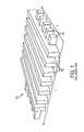
- a replacement metal gate (RMG) processi.e., a gate last process, has been traditionally used in semiconductor fabrications processes to form a semiconductor device including one or more gate elements 102 that wrap around on one or more semiconductor fins 104 .
- the gate elements 102typically extend in a direction perpendicular to the direction of the semiconductor fins 104 as illustrated in FIG. 1 .
- the RMG processutilizes a dummy gate element formed from amorphous silicon (a-Si) or polysilicon (PC), which is ultimately replaced with a metal gate element as understood by those ordinarily skilled in the art.
- the silicon material of the dummy gate elementmay be exposed when recessing the spacers formed on the sidewalls of the dummy gate element. Consequently, epitaxial material may be inadvertently grown on the exposed silicon of the dummy gate element which may result in a short between the epitaxially grown source/drain regions and the epitaxial material grown on the gate element.
- a method of fabricating a semiconductor devicecomprises forming at least one semiconductor fin on a semiconductor substrate.
- a plurality of gate formation layersis formed on an etch stop layer that is formed on one or more of the semiconductor fins.
- the plurality of gate formation layersinclude a dummy gate layer formed from a dielectric material.
- the plurality of gate formation layersis patterned to form a plurality of dummy gate elements on the etch stop layer. Each dummy gate element is formed from the dielectric material.
- a spacer layer formed on the dummy gate elementsis etched to form a spacer on each sidewall of dummy gate elements.
- a portion of the etch stop layer located between each dummy gate elementis etched to expose a portion the semiconductor fin.
- a semiconductor materialis epitaxially grown from the exposed portion of the semiconductor fin to form source/drain regions.
- a method of fabricating a semiconductor devicecomprises forming at least one semiconductor fin on a semiconductor substrate.
- the at least one semiconductor finincludes an etch stop layer formed on an upper surface thereof.
- the methodfurther comprises forming a plurality of dummy gate elements on the etch stop layer.
- Each dummy gate elementis formed from a dielectric material and has a hardmask gate cap formed on an upper surface thereof.
- the methodfurther comprises depositing a high-dielectric layer that conforms to an outer surface of each dummy gate element. A spacer layer is deposited on the high-dielectric layer.
- the methodfurther comprises performing a first etching process that etches the spacer layer to form a spacer on each sidewall of dummy gate elements and exposes an upper portion of the high-dielectric layer.
- the methodfurther comprises performing a second etching process that is different from the first etching process that selectively etches the upper portion of the high-dielectric layer to expose each hardmask gate cap.
- the methodfurther comprises removing the hardmask gate caps and the dummy gate elements to form a trench between a respective pair of spacers.
- the methodfurther comprises performing a third etching process after removing the dummy gates elements to remove a portion of the high-dielectric material from the sidewalls of the spacers such that a remaining portion of the high-dielectric material is interposed between the spacers and the etch stop layer.
- FIG. 1is an isometric view of a conventional array of semiconductor fins having gate elements formed thereon;
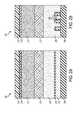
- FIG. 2Ais block diagram of a starting substrate including a plurality of gate formation layers formed on a semiconductor fin according to a first orientation extending along a Y-axis to define a length;
- FIG. 2Billustrates the starting substrate of FIG. 2A according to a second orientation showing the gate formation layers formed on a plurality of semiconductor fins and extending along an X-axis to define a width;
- FIG. 3Aillustrates the substrate of FIGS. 2A-2B according to the first orientation following patterning of a photoresist layer
- FIG. 3Billustrates the substrate of FIG. 3A according to the second orientation
- FIG. 4Aillustrates the substrate of FIGS. 3A-3B according to the first orientation following etching of an optical planar layer and hardmask layer to form individual hardmask gate caps;
- FIG. 4Billustrates the substrate of FIG. 4A according to the second orientation
- FIG. 5Aillustrates the substrate of FIGS. 4A-4B according to the first orientation after etching dummy gate layer according to the patterned hardmask layer to form individual dummy gate elements;
- FIG. 5Billustrates the substrate of FIG. 5A according to the second orientation
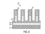
- FIG. 6illustrates the substrate of FIG. 5A following deposition of a conformal spacer layer on sidewalls of the dummy gates elements, gate caps, and on exposed surfaces of the etch stop layer located between each dummy gate element;
- FIG. 7illustrates the substrate of FIG. 6 following an etching process that partially etches the spacer layer formed on the dummy gate element and that removes the spacer layer formed on the etch stop layer;
- FIG. 8illustrates the substrate of FIG. 7 following a pre-clean process that removes a portion of the etch stop layer located between each dummy gate element to expose a portion of the underlying semiconductor fin;
- FIG. 9illustrates the substrate of FIG. 8 following an epitaxial growth process that grows an epitaxial material on the exposed portion of the semiconductor fin located between the dummy gate elements;
- FIG. 10illustrates the substrate of FIG. 9 following deposition of a block dielectric layer that fills the region between the dummy gate elements and that covers the gate caps;
- FIG. 11illustrates the substrate of FIG. 10 following a planarization process that recesses the block dielectric layer and a portion of the spacer layer to expose the dummy gate elements;
- FIG. 12illustrates the substrate of FIG. 11 following removal of the dummy gate elements to form respective gate trenches
- FIG. 13illustrates the substrate of FIG. 12 following a high-dielectric layer deposition and work function metal filling process that fills the trenches with a gate metal to form respective metal gate elements;
- FIG. 14illustrates another exemplary embodiment of the present disclosure where a conformal high-dielectric layer is deposited on sidewalls of the dummy gates elements, gate caps, and on exposed surfaces of the etch stop layer located between each dummy gate element, and a conformal spacer layer is formed on an upper surface of the high-dielectric layer;
- FIG. 15illustrates the substrate of FIG. 14 following an etching process that partially removes the spacer layer formed on the etch stop layer and that etches the spacer layer formed on the dummy gate element to expose an upper portion of the high-dielectric layer;
- FIG. 16illustrates the substrate of FIG. 15 following an etching process that removes an upper portion of the high-dielectric layer
- FIG. 17illustrates the substrate of FIG. 16 following a planarization process that recesses a block dielectric layer and gate caps to expose the dummy gate elements;
- FIG. 18illustrates the substrate of FIG. 17 following removal of the dummy gate elements to form respective gate trenches and to expose the high-dielectric layer formed on sidewalls of the trenches;
- FIG. 19illustrates the substrate of FIG. 18 following an etching process that removes the high-dielectric layer formed on sidewalls of the trenches.
- FIG. 20illustrates the substrate of FIG. 19 following a high-dielectric layer deposition and work function metal filling process that fills the trenches with a gate metal to form respective metal gate elements.
- FIG. 21is a flow diagram illustrating a method of fabricating a semiconductor device according to an exemplary embodiment of the present disclosure.
- a starting semiconductor substrate 200 including a plurality of gate formation layers formed on one or more semiconductor fins 202is illustrated according to an exemplary embodiment of the present disclosure.
- the substrate 200extends along an X-axis to define a width and a Y-axis to define a length.
- the semiconductor fins 202may be formed on a buried oxide (BOX) layer 204 formed on the substrate 200 . It is appreciated, however, that the semiconductor fins 202 may be formed on a bulk semiconductor layer of the substrate 200 .
- An etch stop layer 206may be formed on an upper surface of the semiconductor fins 202 .
- the BOX layer and the etch stop layermay be formed from a dielectric material including, but not limited to, silicon oxide (SiO 2 ).
- a finFET semiconductor deviceis described going forward, it is appreciated that the inventive teachings described herein may be applied to various other semiconductor topologies including, but not limited to, a planar semiconductor device, and a nanowire semiconductor device.
- the gate formation layersare formed on an upper surface of the etch stop layer 206 formed on each semiconductor fin 202 .
- the plurality of gate formation layersinclude, for example, a dummy gate dielectric layer 208 , a gate hardmask layer 210 , an optical planar layer (OPL) 212 , an anti-reflective coating (ARC) layer 214 , and a photoresist layer 216 .
- OPLoptical planar layer
- ARCanti-reflective coating
- the ARC layer 214may be replaced with a silicon oxide layer.
- the dummy gate dielectric layer 208may be formed directly on an upper surface of the etch stop layer 206 , for example. Unlike a conventional replacement metal gate (RMG) process, the dummy gate dielectric layer 208 is formed from a dielectric material instead of amorphous silicon (Si) or polysilicon (PC).
- the dummy gate dielectric layer 208may be formed from various materials including, but not limited to, boron carbide (BC), a silicon boron carbide material that contains nitrogen (i.e., SiB:C(N)), carbon (C), compressed carbon, and SiO 2 . Therefore, at least one exemplary embodiment of the present disclosure may prevent inadvertent epitaxially growth on exposed portions of the dummy gate element (described below). Accordingly, shorting between epitaxially grown source-drain regions and the dummy gate element may be prevented.
- BCboron carbide
- SiB:C(N)silicon boron carbide material that contains nitrogen (i.e., SiB
- the gate hardmask layer 210is stacked on the dummy gate dielectric layer 208 and may be formed from various materials including, but not limited to, silicon nitride (SiN) and silicon dioxide (SiO 2 ).
- the OPL 212is stacked on the gate hardmask layer 210 to form a planarized upper surface.
- the OPL 212may be formed from an organic dielectric layer (ODL) material including, but not limited to, amorphous carbon, CHM701B, commercially available from Cheil Chemical Co., Ltd., HM8006 and HM8014, commercially available from JSR Corporation, and ODL-102, commercially available from ShinEtsu Chemical, Co., Ltd.
- ODLorganic dielectric layer
- the SiARC layer 214is stacked on the OPL 212 and may comprise Si, for example, to form a silicon-containing ARC (SiARC) layer as described going forward.
- the photoresist layer 216may be deposited according to a chemical vapor deposition (CVD) process or an atomic layer deposition (ALD) process as understood by those ordinarily skilled in the art.
- the photoresist layer 216is patterned to form one or more individual gate resist elements 218 .
- the gate resist elements 218ultimately determine the pattern of respective dummy gate elements to be formed on the substrate 200 as understood by those ordinarily skilled in the art.
- the stacked arrangement of the photoresist layer 216 , the SiARC layer 214 and the OPL 212may form a multilayer element (e.g., a trilateral element) such that a trilayer resist (TLR) patterning scheme may be performed that forms one or more dummy gate elements.
- TLRtrilayer resist
- the TLR pattering schemecomprises, for example, patterning the photoresist layer 216 using lithography and trimming, performing first a reactive ion etching (RIE) plasma process to etch through the SiARC layer 214 utilizing the patterned photoresist layer 216 (i.e., the gate resist elements 218 ) as a first pattern mask where a portion of the photoresist layer 216 is consumed during the during first etching, performing a second etching process to etch the ODL utilizing the patterned SiARC layer 214 as a second pattern mask where the photoresist layer 216 is completely consumed during the second etching, performing a third etching process to remove (e.g., burn-off) the SiARC layer 214 , performing a fourth etching process to etch the gate hardmask layer 210 utilizing the etched ODL as a third pattern mask where a portion of the gate hardmask layer 210 is removed during the third etching such that individual hardmask gate caps 2
- RIEreactive
- the dummy gate dielectric layer 208is patterned according to the patterned gate hardmask layer 210 (i.e., the hardmask gate caps 220 ) to form individual dummy gate elements 222 .
- the dummy gate dielectric layer 208may be etched using a reactive ion etching (RIE) process as understood by those ordinarily skilled in the art. Accordingly, one or more individual dummy gate elements 222 are formed that wrap around one or more semiconductor fins 202 .
- RIEreactive ion etching
- a conformal spacer layer 224is deposited on sidewalls of the dummy gates elements 222 , hardmask gate caps 220 , and on exposed surfaces of the etch stop layer 206 located between each dummy gate element 222 .
- the conformal spacer layer 224may be formed from, for example, silicon nitride (SiN).
- the spacer layer 224 formed on the dummy gate element 222is partially etched such that spacers 226 are formed on sidewalls of the dummy gate element 222 .
- Various etching processesmay be used to etch the spacer layer 224 including, but not limited to, RIE.
- a portion of the spacer layer 224 formed on the hardmask gate cap 220may also be removed such that the underlying gate cap 220 is exposed as further illustrated in FIG. 7 .
- a pre-clean processis performed that removes a portion of the etch stop layer 206 located between each dummy gate element 222 . Accordingly, a cavity 228 is formed between each dummy gate element 222 , which exposes a portion of the underlying semiconductor fin 202 .
- the pre-clean processmay be performed using a hydrogen fluoride (HF) based wet clean process, or a dry etching process that uses remote plasma that reacts with the etch stop layer 206 , while being selective to the spacers 226 .
- HFhydrogen fluoride
- an epitaxial growth processis performed that grows an epitaxial semiconductor material 230 on the exposed portion of the semiconductor fin 202 located between the dummy gate elements 222 .
- Well-known processes used to epitaxially grow an epitaxial semiconductor material 230including, but not limited to, silicon doped with germanium (Ge), carbon (C), and phosphorus (P), or any dopants desired to lower external resistance for forming a source/drain region.
- the epitaxial semiconductor material 230may be grown from a portion of the semiconductor fin 202 exposed by a respective cavity 228 and may extend therefrom to contact the sidewalls of a pair of opposing spacers 226 to form one or more source/drain regions.
- a contact dielectric layer 232is deposited on the hardmask gate caps 220 and in the voids between the dummy gate elements 222 .
- the contact dielectric layer 232may also contact one or more source/drain regions of one or more semiconductor fins 202 .
- Various methodsmay be used to deposit the contact dielectric layer 232 including, but not limited to, chemical vapor deposition (CVD) and atomic layer deposition (ALD).
- the contact dielectric layer 232may be formed from various materials including, but not limited to, SiO 2 .
- a planarization processis performed, which partially recesses the contact dielectric layer 232 and a portion of the spacer layer 224 to expose the dummy gate elements 222 .
- the planarization processmay stop on the upper surface of the dummy gate elements 222 such that the upper surface of the contact dielectric layer 232 is flush with the upper surfaces of the dummy gate elements 222 .
- the dummy gate elements 222are removed according to a replacement metal gate (RMG) process as understood by those ordinarily skilled in the art.
- the dummy gate elements 222may be removed using an RIE process or a wet etching process. Accordingly, gate trenches 234 that expose the underlying etch stop layer 206 of the semiconductor fin 202 are formed between a respective pair of spacers 226 .
- an anneal processmay be performed after removing the dummy gate elements 222 to activate the dopants of the source/drain regions. The anneal process may generate a temperature of approximately 900 degrees Celsius (C) or higher, for example.
- a metal filling processis performed that fills the trenches with a gate metal to form respective metal gate elements 236 .
- the gate metalmay include various metal materials including, but not limited to, tungsten (W), tantalum (Ta), titanium (Ti), Niobium (Nb), rhenium (Rh), aluminum (Al), tungsten nitride (WN), titanium nitride (TiN) and tantalum nitride (TaN).
- each metalmay contact a respective pair of spacers 226 and a respective etch stop layer 206 .
- one or more work function metal (WFM) layersmay be deposited in the trenches 234 and formed on the sidewalls of the spacers 226 before filling the trenches 234 with the metal gate material.
- the WFM layermay tune the threshold voltage of a resulting semiconductor device as understood by those ordinarily skilled in the art.
- FIGS. 14-20a process flow that interposes a high-dielectric constant layer 238 (i.e., a high-k layer 238 ) between the spacers 226 and the sidewalls of each dummy gate element 222 is illustrated according to an exemplary embodiment of the present disclosure.
- FIG. 14illustrates a conformal high-k layer 238 interposed between a conformal spacer layer 224 and the dummy gate elements 222 .
- the conformal high-k layer 238may first be deposited on sidewalls of the dummy gates elements 222 , hardmask gate caps 220 , and exposed surfaces of the etch stop layer 206 located between each dummy gate element 222 .
- the high-k layer 238may be formed from various high-k materials including, but not limited to, hafnium oxide (HfO 2 ).
- the conformal spacer layer 224may then be formed on an upper surface of the high-k layer 238 .
- the conformal spacer layer 224may be formed from, for example, SiN.
- an etching processis performed that partially removes the spacer layer 224 formed on the etch stop layer 206 and that etches the spacer layer 224 formed on the dummy gate element 222 . Accordingly, an upper portion of the high-k layer 238 is exposed.
- a second etching processsuch as a carina etch for example, is performed that removes the exposed upper portion of the high-k layer 238 .
- the carina etchis selective to the spacer layer 224 such that the high-k layer 238 is removed while the spacer layer 224 is maintained. Accordingly, an upper portion of the underlying hardmask gate cap 220 is exposed.
- a planarization process that partially recesses a contact dielectric layer 232is performed which exposes an upper portion of the dummy gate elements 222 .
- the contact dielectric layer 232is formed as previously discussed above.
- the planarization processmay stop on the upper surface of the dummy gate elements 222 such that the upper surface of the contact dielectric layer 232 is flush with the upper surfaces of the dummy gate elements 222 .
- the dummy gate elements 222are removed according to a replacement metal gate (RMG) process as understood by those ordinarily skilled in the art.
- RMGreplacement metal gate
- an RIE process or a wet etching processmay be used to remove the dummy gate elements 222 .
- gate trenches 234are formed that expose portions of the underlying etch stop layer 206 located between the remaining high-k layer 238 formed on sidewalls of the spacers 226 .
- an etching processis performed that removes portions of the high-k layer 238 from the sidewalls of the spacers 226 such that the length of each trench 234 increases.
- Various etchings processmay be used to remove the high-k layer 238 including, but not limited to, a carina etch.
- a portion of the high-k layer 238 ′may be maintained between the spacer 226 and the etch stop layer 206 , while the trench 234 exposes a portion of the etch stop layer 206 located between the spacers 226 .
- at least one exemplary embodiment of the present teachingsutilizes the high-k layer 238 as a gate oxide layer.
- the properties of the high-k layer 238may change during the dummy gate pull process to affect work function properties.
- the high-k layer 238may be best used as a sacrificial layer and may be omitted at FIG. 19 , and deposited as a high-k gate oxide layer before performing a metal filling process described below. Accordingly, process of removing portions of the high-k layer 238 from the sidewalls is optional and may be skipped at this stage of the exemplary process flow.
- the gate metalmay include various metal materials including, but not limited to, tungsten (W), tantalum (Ta), titanium (Ti), Niobium (Nb), rhenium (Rh), aluminum (Al), tungsten nitride (WN), titanium nitride (TiN) and tantalum nitride (TaN).
- the metal gate elements 236may contact the spacers 226 , the remaining high-k material, and the etch stop layer 206 .
- a high-k layer 238 for forming a gate oxide layermay be deposited in the trenches 234 before depositing the gate metal in the trenches 234 .
- FIG. 21is a flow diagram illustrating a method of fabricating a semiconductor device according to an exemplary embodiment of the present disclosure.
- the methodbegins at operation 2100 , and proceeds to operation 2102 where a plurality of gate formation layers are formed on one or more semiconductor fins.
- the semiconductor finsare formed on a semiconductor substrate as understood by those ordinarily skilled in the art.
- the plurality of gate formation layersare etched such that a one or more hardmask gate caps are patterned atop a dummy gate dielectric layer.
- a trilayer resist (TLR) patterning schememay be used to etch the gate formation layer, for example.
- TLRtrilayer resist
- the dummy gate dielectric layeris etched to form one or more dummy gate elements having a respective hardmask gate cap formed on an upper surface thereof.
- the pattern of the one or more gate elementsmay be based on a pattern of the one or more hardmask gate caps previously formed atop the dummy gate dielectric layer.
- a conformal spacer layeris deposited on sidewalls of the dummy gates elements, the gate caps, and on the exposed surfaces of the etch stop layer located between each dummy gate element.
- a conformal high-k layermay be deposited on sidewalls of the dummy gates elements, the gate caps, and on the exposed surfaces of the etch stop layer located between each dummy gate element.
- the conformal spacer layeris deposited on top of the high-k layer.
- the high-k layeris interposed between the dummy gate elements and the spacer layer.
- the spacer layer formed on the dummy gate elementis partially etched such that the spacers are formed on the sidewalls of the dummy gate element and a portion of the underlying gate cap is exposed.
- a pre-clean processis performed that removes a portion of the etch stop layer located between each dummy gate element. Accordingly, a portion of the underlying semiconductor fin located between each dummy gate element is exposed.
- an epitaxial materialis grown on the exposed portion of the semiconductor fin located between the dummy gate elements.
- a contact dielectric layeris deposited on the gate caps and in the voids between the dummy gate elements.
- a portion of contact dielectric layer and a portion of the spacersare recessed using, for example, a chemical mechanical planarization (CMP) process.
- CMPchemical mechanical planarization
- the planarization processmay stop on the upper surface of the dummy gate elements such that the upper surface of the contact dielectric layer is flush with the upper surfaces of the dummy gate elements.
- the dummy gate elementsare removed according to a replacement metal gate (RMG) process as understood by those ordinarily skilled in the art.
- RMGreplacement metal gate
- a wet etching process or RIE processmay be used to remove the dummy gate elements.
- gate trenches that expose the underlying etch stop layerare formed between a respective pair of spacers.
- the trenchesare filled with a metal gate material to form respective metal gate elements, and the method ends at operation 2124 .
Landscapes
- Engineering & Computer Science (AREA)
- Physics & Mathematics (AREA)
- Microelectronics & Electronic Packaging (AREA)
- General Physics & Mathematics (AREA)
- Manufacturing & Machinery (AREA)
- Computer Hardware Design (AREA)
- Condensed Matter Physics & Semiconductors (AREA)
- Power Engineering (AREA)
- Chemical & Material Sciences (AREA)
- Chemical Kinetics & Catalysis (AREA)
- General Chemical & Material Sciences (AREA)
- Inorganic Chemistry (AREA)
- Plasma & Fusion (AREA)
- Insulated Gate Type Field-Effect Transistor (AREA)
- Electrodes Of Semiconductors (AREA)
Abstract
Description
- The present invention relates to semiconductor device fabrication, and in particular, to a replacement metal gate process.
- A replacement metal gate (RMG) process, i.e., a gate last process, has been traditionally used in semiconductor fabrications processes to form a semiconductor device including one or
more gate elements 102 that wrap around on one ormore semiconductor fins 104. Thegate elements 102 typically extend in a direction perpendicular to the direction of thesemiconductor fins 104 as illustrated inFIG. 1 . The RMG process utilizes a dummy gate element formed from amorphous silicon (a-Si) or polysilicon (PC), which is ultimately replaced with a metal gate element as understood by those ordinarily skilled in the art. However, the silicon material of the dummy gate element may be exposed when recessing the spacers formed on the sidewalls of the dummy gate element. Consequently, epitaxial material may be inadvertently grown on the exposed silicon of the dummy gate element which may result in a short between the epitaxially grown source/drain regions and the epitaxial material grown on the gate element. - According to at least one embodiment a method of fabricating a semiconductor device comprises forming at least one semiconductor fin on a semiconductor substrate. A plurality of gate formation layers is formed on an etch stop layer that is formed on one or more of the semiconductor fins. The plurality of gate formation layers include a dummy gate layer formed from a dielectric material. The plurality of gate formation layers is patterned to form a plurality of dummy gate elements on the etch stop layer. Each dummy gate element is formed from the dielectric material. A spacer layer formed on the dummy gate elements is etched to form a spacer on each sidewall of dummy gate elements. A portion of the etch stop layer located between each dummy gate element is etched to expose a portion the semiconductor fin. A semiconductor material is epitaxially grown from the exposed portion of the semiconductor fin to form source/drain regions.
- According to another exemplary embodiment, a method of fabricating a semiconductor device comprises forming at least one semiconductor fin on a semiconductor substrate. The at least one semiconductor fin includes an etch stop layer formed on an upper surface thereof. The method further comprises forming a plurality of dummy gate elements on the etch stop layer. Each dummy gate element is formed from a dielectric material and has a hardmask gate cap formed on an upper surface thereof. The method further comprises depositing a high-dielectric layer that conforms to an outer surface of each dummy gate element. A spacer layer is deposited on the high-dielectric layer. The method further comprises performing a first etching process that etches the spacer layer to form a spacer on each sidewall of dummy gate elements and exposes an upper portion of the high-dielectric layer. The method further comprises performing a second etching process that is different from the first etching process that selectively etches the upper portion of the high-dielectric layer to expose each hardmask gate cap. The method further comprises removing the hardmask gate caps and the dummy gate elements to form a trench between a respective pair of spacers. The method further comprises performing a third etching process after removing the dummy gates elements to remove a portion of the high-dielectric material from the sidewalls of the spacers such that a remaining portion of the high-dielectric material is interposed between the spacers and the etch stop layer.
- Additional features are realized through the techniques of the present invention. Other embodiments are described in detail herein and are considered a part of the claimed invention. For a better understanding of the invention with the features, refer to the description and to the drawings.
- The subject matter which is regarded as the invention is particularly pointed out and distinctly claimed in the claims at the conclusion of the specification. The forgoing features are apparent from the following detailed description taken in conjunction with the accompanying drawings in which:
FIG. 1 is an isometric view of a conventional array of semiconductor fins having gate elements formed thereon;FIG. 2A is block diagram of a starting substrate including a plurality of gate formation layers formed on a semiconductor fin according to a first orientation extending along a Y-axis to define a length;FIG. 2B illustrates the starting substrate ofFIG. 2A according to a second orientation showing the gate formation layers formed on a plurality of semiconductor fins and extending along an X-axis to define a width;FIG. 3A illustrates the substrate ofFIGS. 2A-2B according to the first orientation following patterning of a photoresist layer;FIG. 3B illustrates the substrate ofFIG. 3A according to the second orientation;FIG. 4A illustrates the substrate ofFIGS. 3A-3B according to the first orientation following etching of an optical planar layer and hardmask layer to form individual hardmask gate caps;FIG. 4B illustrates the substrate ofFIG. 4A according to the second orientation;FIG. 5A illustrates the substrate ofFIGS. 4A-4B according to the first orientation after etching dummy gate layer according to the patterned hardmask layer to form individual dummy gate elements;FIG. 5B illustrates the substrate ofFIG. 5A according to the second orientation;FIG. 6 illustrates the substrate ofFIG. 5A following deposition of a conformal spacer layer on sidewalls of the dummy gates elements, gate caps, and on exposed surfaces of the etch stop layer located between each dummy gate element;FIG. 7 illustrates the substrate ofFIG. 6 following an etching process that partially etches the spacer layer formed on the dummy gate element and that removes the spacer layer formed on the etch stop layer;FIG. 8 illustrates the substrate ofFIG. 7 following a pre-clean process that removes a portion of the etch stop layer located between each dummy gate element to expose a portion of the underlying semiconductor fin;FIG. 9 illustrates the substrate ofFIG. 8 following an epitaxial growth process that grows an epitaxial material on the exposed portion of the semiconductor fin located between the dummy gate elements;FIG. 10 illustrates the substrate ofFIG. 9 following deposition of a block dielectric layer that fills the region between the dummy gate elements and that covers the gate caps;FIG. 11 illustrates the substrate ofFIG. 10 following a planarization process that recesses the block dielectric layer and a portion of the spacer layer to expose the dummy gate elements;FIG. 12 illustrates the substrate ofFIG. 11 following removal of the dummy gate elements to form respective gate trenches;FIG. 13 illustrates the substrate ofFIG. 12 following a high-dielectric layer deposition and work function metal filling process that fills the trenches with a gate metal to form respective metal gate elements;FIG. 14 illustrates another exemplary embodiment of the present disclosure where a conformal high-dielectric layer is deposited on sidewalls of the dummy gates elements, gate caps, and on exposed surfaces of the etch stop layer located between each dummy gate element, and a conformal spacer layer is formed on an upper surface of the high-dielectric layer;FIG. 15 illustrates the substrate ofFIG. 14 following an etching process that partially removes the spacer layer formed on the etch stop layer and that etches the spacer layer formed on the dummy gate element to expose an upper portion of the high-dielectric layer;FIG. 16 illustrates the substrate ofFIG. 15 following an etching process that removes an upper portion of the high-dielectric layer;FIG. 17 illustrates the substrate ofFIG. 16 following a planarization process that recesses a block dielectric layer and gate caps to expose the dummy gate elements;FIG. 18 illustrates the substrate ofFIG. 17 following removal of the dummy gate elements to form respective gate trenches and to expose the high-dielectric layer formed on sidewalls of the trenches;FIG. 19 illustrates the substrate ofFIG. 18 following an etching process that removes the high-dielectric layer formed on sidewalls of the trenches; andFIG. 20 illustrates the substrate ofFIG. 19 following a high-dielectric layer deposition and work function metal filling process that fills the trenches with a gate metal to form respective metal gate elements.FIG. 21 is a flow diagram illustrating a method of fabricating a semiconductor device according to an exemplary embodiment of the present disclosure.- With reference now to
FIGS. 2A-2B , a startingsemiconductor substrate 200 including a plurality of gate formation layers formed on one ormore semiconductor fins 202 is illustrated according to an exemplary embodiment of the present disclosure. Thesubstrate 200 extends along an X-axis to define a width and a Y-axis to define a length. Thesemiconductor fins 202 may be formed on a buried oxide (BOX)layer 204 formed on thesubstrate 200. It is appreciated, however, that thesemiconductor fins 202 may be formed on a bulk semiconductor layer of thesubstrate 200. Anetch stop layer 206 may be formed on an upper surface of thesemiconductor fins 202. The BOX layer and the etch stop layer may be formed from a dielectric material including, but not limited to, silicon oxide (SiO2). Although a finFET semiconductor device is described going forward, it is appreciated that the inventive teachings described herein may be applied to various other semiconductor topologies including, but not limited to, a planar semiconductor device, and a nanowire semiconductor device. - The gate formation layers are formed on an upper surface of the
etch stop layer 206 formed on eachsemiconductor fin 202. The plurality of gate formation layers include, for example, a dummygate dielectric layer 208, agate hardmask layer 210, an optical planar layer (OPL)212, an anti-reflective coating (ARC)layer 214, and aphotoresist layer 216. Although not illustrated, TheARC layer 214 may be replaced with a silicon oxide layer. - The dummy
gate dielectric layer 208 may be formed directly on an upper surface of theetch stop layer 206, for example. Unlike a conventional replacement metal gate (RMG) process, the dummygate dielectric layer 208 is formed from a dielectric material instead of amorphous silicon (Si) or polysilicon (PC). The dummygate dielectric layer 208 may be formed from various materials including, but not limited to, boron carbide (BC), a silicon boron carbide material that contains nitrogen (i.e., SiB:C(N)), carbon (C), compressed carbon, and SiO2. Therefore, at least one exemplary embodiment of the present disclosure may prevent inadvertent epitaxially growth on exposed portions of the dummy gate element (described below). Accordingly, shorting between epitaxially grown source-drain regions and the dummy gate element may be prevented. - The
gate hardmask layer 210 is stacked on the dummygate dielectric layer 208 and may be formed from various materials including, but not limited to, silicon nitride (SiN) and silicon dioxide (SiO2). TheOPL 212 is stacked on thegate hardmask layer 210 to form a planarized upper surface. TheOPL 212 may be formed from an organic dielectric layer (ODL) material including, but not limited to, amorphous carbon, CHM701B, commercially available from Cheil Chemical Co., Ltd., HM8006 and HM8014, commercially available from JSR Corporation, and ODL-102, commercially available from ShinEtsu Chemical, Co., Ltd. - The
SiARC layer 214 is stacked on theOPL 212 and may comprise Si, for example, to form a silicon-containing ARC (SiARC) layer as described going forward. Thephotoresist layer 216 may be deposited according to a chemical vapor deposition (CVD) process or an atomic layer deposition (ALD) process as understood by those ordinarily skilled in the art. - Referring to
FIGS. 3A-3B , thephotoresist layer 216 is patterned to form one or more individual gate resistelements 218. The gate resistelements 218 ultimately determine the pattern of respective dummy gate elements to be formed on thesubstrate 200 as understood by those ordinarily skilled in the art. The stacked arrangement of thephotoresist layer 216, theSiARC layer 214 and theOPL 212 may form a multilayer element (e.g., a trilateral element) such that a trilayer resist (TLR) patterning scheme may be performed that forms one or more dummy gate elements. - According to at least embodiment, the TLR pattering scheme comprises, for example, patterning the
photoresist layer 216 using lithography and trimming, performing first a reactive ion etching (RIE) plasma process to etch through theSiARC layer 214 utilizing the patterned photoresist layer216 (i.e., the gate resist elements218) as a first pattern mask where a portion of thephotoresist layer 216 is consumed during the during first etching, performing a second etching process to etch the ODL utilizing the patternedSiARC layer 214 as a second pattern mask where thephotoresist layer 216 is completely consumed during the second etching, performing a third etching process to remove (e.g., burn-off) theSiARC layer 214, performing a fourth etching process to etch thegate hardmask layer 210 utilizing the etched ODL as a third pattern mask where a portion of thegate hardmask layer 210 is removed during the third etching such that individual hardmask gate caps220 are formed on the dummygate dielectric layer 208, and stripping the etched ODL using an RIE or wet cleaning process to form one or more individual hardmask gate caps220 on the dummygate dielectric layer 208 as illustrated inFIGS. 4A-4B . Accordingly, the pattern of thephotoresist layer 216 may be transferred to thegate hardmask layer 210 for ultimately forming the pattern of dummy gate elements as discussed in greater detail below - Referring to
FIGS. 5A-5B , the dummygate dielectric layer 208 is patterned according to the patterned gate hardmask layer210 (i.e., the hardmask gate caps220) to form individualdummy gate elements 222. The dummygate dielectric layer 208 may be etched using a reactive ion etching (RIE) process as understood by those ordinarily skilled in the art. Accordingly, one or more individualdummy gate elements 222 are formed that wrap around one ormore semiconductor fins 202. - Turning now to
FIG. 6 , aconformal spacer layer 224 is deposited on sidewalls of thedummy gates elements 222, hardmask gate caps220, and on exposed surfaces of theetch stop layer 206 located between eachdummy gate element 222. Theconformal spacer layer 224 may be formed from, for example, silicon nitride (SiN). - Referring to
FIG. 7 , thespacer layer 224 formed on thedummy gate element 222 is partially etched such thatspacers 226 are formed on sidewalls of thedummy gate element 222. Various etching processes may be used to etch thespacer layer 224 including, but not limited to, RIE. A portion of thespacer layer 224 formed on thehardmask gate cap 220 may also be removed such that theunderlying gate cap 220 is exposed as further illustrated inFIG. 7 . - Referring to
FIG. 8 , a pre-clean process is performed that removes a portion of theetch stop layer 206 located between eachdummy gate element 222. Accordingly, acavity 228 is formed between eachdummy gate element 222, which exposes a portion of theunderlying semiconductor fin 202. The pre-clean process may be performed using a hydrogen fluoride (HF) based wet clean process, or a dry etching process that uses remote plasma that reacts with theetch stop layer 206, while being selective to thespacers 226. - Turning now to
FIG. 9 , an epitaxial growth process is performed that grows anepitaxial semiconductor material 230 on the exposed portion of thesemiconductor fin 202 located between thedummy gate elements 222. Well-known processes used to epitaxially grow anepitaxial semiconductor material 230 including, but not limited to, silicon doped with germanium (Ge), carbon (C), and phosphorus (P), or any dopants desired to lower external resistance for forming a source/drain region. Theepitaxial semiconductor material 230 may be grown from a portion of thesemiconductor fin 202 exposed by arespective cavity 228 and may extend therefrom to contact the sidewalls of a pair of opposingspacers 226 to form one or more source/drain regions. - Referring to
FIG. 10 , acontact dielectric layer 232 is deposited on the hardmask gate caps220 and in the voids between thedummy gate elements 222. Thecontact dielectric layer 232 may also contact one or more source/drain regions of one ormore semiconductor fins 202. Various methods may be used to deposit thecontact dielectric layer 232 including, but not limited to, chemical vapor deposition (CVD) and atomic layer deposition (ALD). Thecontact dielectric layer 232 may be formed from various materials including, but not limited to, SiO2. - Referring now to
FIG. 11 , a planarization process is performed, which partially recesses thecontact dielectric layer 232 and a portion of thespacer layer 224 to expose thedummy gate elements 222. The planarization process may stop on the upper surface of thedummy gate elements 222 such that the upper surface of thecontact dielectric layer 232 is flush with the upper surfaces of thedummy gate elements 222. - Turning to
FIG. 12 , thedummy gate elements 222 are removed according to a replacement metal gate (RMG) process as understood by those ordinarily skilled in the art. For example, thedummy gate elements 222 may be removed using an RIE process or a wet etching process. Accordingly,gate trenches 234 that expose the underlyingetch stop layer 206 of thesemiconductor fin 202 are formed between a respective pair ofspacers 226. According to at least one embodiment, an anneal process may be performed after removing thedummy gate elements 222 to activate the dopants of the source/drain regions. The anneal process may generate a temperature of approximately 900 degrees Celsius (C) or higher, for example. - Referring to
FIG. 13 , a metal filling process is performed that fills the trenches with a gate metal to form respectivemetal gate elements 236. The gate metal may include various metal materials including, but not limited to, tungsten (W), tantalum (Ta), titanium (Ti), Niobium (Nb), rhenium (Rh), aluminum (Al), tungsten nitride (WN), titanium nitride (TiN) and tantalum nitride (TaN). According to this exemplary embodiment, each metal may contact a respective pair ofspacers 226 and a respectiveetch stop layer 206. In another embodiment, one or more work function metal (WFM) layers may be deposited in thetrenches 234 and formed on the sidewalls of thespacers 226 before filling thetrenches 234 with the metal gate material. The WFM layer may tune the threshold voltage of a resulting semiconductor device as understood by those ordinarily skilled in the art. - Turning now to
FIGS. 14-20 , a process flow that interposes a high-dielectric constant layer238 (i.e., a high-k layer238) between thespacers 226 and the sidewalls of eachdummy gate element 222 is illustrated according to an exemplary embodiment of the present disclosure. In this regard,FIG. 14 illustrates a conformal high-k layer 238 interposed between aconformal spacer layer 224 and thedummy gate elements 222. The conformal high-k layer 238 may first be deposited on sidewalls of thedummy gates elements 222, hardmask gate caps220, and exposed surfaces of theetch stop layer 206 located between eachdummy gate element 222. The high-k layer 238 may be formed from various high-k materials including, but not limited to, hafnium oxide (HfO2). Theconformal spacer layer 224 may then be formed on an upper surface of the high-k layer 238. Theconformal spacer layer 224 may be formed from, for example, SiN. - Referring to
FIG. 15 , an etching process is performed that partially removes thespacer layer 224 formed on theetch stop layer 206 and that etches thespacer layer 224 formed on thedummy gate element 222. Accordingly, an upper portion of the high-k layer 238 is exposed. - Referring to
FIG. 16 , a second etching process, such as a carina etch for example, is performed that removes the exposed upper portion of the high-k layer 238. The carina etch is selective to thespacer layer 224 such that the high-k layer 238 is removed while thespacer layer 224 is maintained. Accordingly, an upper portion of the underlyinghardmask gate cap 220 is exposed. - Referring to
FIG. 17 , a planarization process that partially recesses acontact dielectric layer 232 is performed which exposes an upper portion of thedummy gate elements 222. Thecontact dielectric layer 232 is formed as previously discussed above. The planarization process may stop on the upper surface of thedummy gate elements 222 such that the upper surface of thecontact dielectric layer 232 is flush with the upper surfaces of thedummy gate elements 222. - Referring now to
FIG. 18 , thedummy gate elements 222 are removed according to a replacement metal gate (RMG) process as understood by those ordinarily skilled in the art. For example, an RIE process or a wet etching process may be used to remove thedummy gate elements 222. Accordingly,gate trenches 234 are formed that expose portions of the underlyingetch stop layer 206 located between the remaining high-k layer 238 formed on sidewalls of thespacers 226. - Referring to
FIG. 19 , an etching process is performed that removes portions of the high-k layer 238 from the sidewalls of thespacers 226 such that the length of eachtrench 234 increases. Various etchings process may be used to remove the high-k layer 238 including, but not limited to, a carina etch. As illustrated inFIG. 19 , for example, a portion of the high-k layer 238′ may be maintained between thespacer 226 and theetch stop layer 206, while thetrench 234 exposes a portion of theetch stop layer 206 located between thespacers 226. Although not illustrated, at least one exemplary embodiment of the present teachings utilizes the high-k layer 238 as a gate oxide layer. In this regard, the properties of the high-k layer 238 may change during the dummy gate pull process to affect work function properties. For purpose of gate work function control, the high-k layer 238 may be best used as a sacrificial layer and may be omitted atFIG. 19 , and deposited as a high-k gate oxide layer before performing a metal filling process described below. Accordingly, process of removing portions of the high-k layer 238 from the sidewalls is optional and may be skipped at this stage of the exemplary process flow. - Turning now to
FIG. 20 , a metal filling process is performed that fills thetrenches 234 with a gate metal to form respectivemetal gate elements 236. The gate metal may include various metal materials including, but not limited to, tungsten (W), tantalum (Ta), titanium (Ti), Niobium (Nb), rhenium (Rh), aluminum (Al), tungsten nitride (WN), titanium nitride (TiN) and tantalum nitride (TaN). According to this exemplary embodiment, themetal gate elements 236 may contact thespacers 226, the remaining high-k material, and theetch stop layer 206. As discussed above, a high-k layer 238 for forming a gate oxide layer may be deposited in thetrenches 234 before depositing the gate metal in thetrenches 234. FIG. 21 is a flow diagram illustrating a method of fabricating a semiconductor device according to an exemplary embodiment of the present disclosure. The method begins atoperation 2100, and proceeds tooperation 2102 where a plurality of gate formation layers are formed on one or more semiconductor fins. The semiconductor fins are formed on a semiconductor substrate as understood by those ordinarily skilled in the art. Atoperation 2104, the plurality of gate formation layers are etched such that a one or more hardmask gate caps are patterned atop a dummy gate dielectric layer. A trilayer resist (TLR) patterning scheme may be used to etch the gate formation layer, for example. Atoperation 2106, the dummy gate dielectric layer is etched to form one or more dummy gate elements having a respective hardmask gate cap formed on an upper surface thereof. The pattern of the one or more gate elements may be based on a pattern of the one or more hardmask gate caps previously formed atop the dummy gate dielectric layer. Atoperation 2108, a conformal spacer layer is deposited on sidewalls of the dummy gates elements, the gate caps, and on the exposed surfaces of the etch stop layer located between each dummy gate element. According to another exemplary embodiment, a conformal high-k layer may be deposited on sidewalls of the dummy gates elements, the gate caps, and on the exposed surfaces of the etch stop layer located between each dummy gate element. Thereafter, the conformal spacer layer is deposited on top of the high-k layer. In this regard, the high-k layer is interposed between the dummy gate elements and the spacer layer.- Turning to
operation 2110, the spacer layer formed on the dummy gate element is partially etched such that the spacers are formed on the sidewalls of the dummy gate element and a portion of the underlying gate cap is exposed. Atoperation 2112, a pre-clean process is performed that removes a portion of the etch stop layer located between each dummy gate element. Accordingly, a portion of the underlying semiconductor fin located between each dummy gate element is exposed. Atoperation 2114, an epitaxial material is grown on the exposed portion of the semiconductor fin located between the dummy gate elements. Atoperation 2116, a contact dielectric layer is deposited on the gate caps and in the voids between the dummy gate elements. Atoperation 2118, a portion of contact dielectric layer and a portion of the spacers are recessed using, for example, a chemical mechanical planarization (CMP) process. The planarization process may stop on the upper surface of the dummy gate elements such that the upper surface of the contact dielectric layer is flush with the upper surfaces of the dummy gate elements. Atoperation 2120, the dummy gate elements are removed according to a replacement metal gate (RMG) process as understood by those ordinarily skilled in the art. For example, a wet etching process or RIE process may be used to remove the dummy gate elements. Accordingly, gate trenches that expose the underlying etch stop layer are formed between a respective pair of spacers. Atoperation 2122, the trenches are filled with a metal gate material to form respective metal gate elements, and the method ends atoperation 2124. - The terminology used herein is for the purpose of describing particular embodiments only and is not intended to be limiting of the invention. As used herein, the singular forms “a”, “an” and “the” are intended to include the plural forms as well, unless the context clearly indicates otherwise. It will be further understood that the terms “comprises” and/or “comprising,” when used in this specification, specify the presence of stated features, integers, steps, operations, elements, and/or components, but do not preclude the presence or addition of one more other features, integers, steps, operations, element components, and/or groups thereof.
- The corresponding structures, materials, acts, and equivalents of all means or step plus function elements in the claims below are intended to include any structure, material, or act for performing the function in combination with other claimed elements as specifically claimed. The description of the present invention has been presented for purposes of illustration and description, but is not intended to be exhaustive or limited to the invention in the form disclosed. Many modifications and variations will be apparent to those of ordinary skill in the art without departing from the scope and spirit of the invention. The embodiment was chosen and described in order to best explain the principles of the inventive teachings and the practical application, and to enable others of ordinary skill in the art to understand the invention for various embodiments with various modifications as are suited to the particular use contemplated.
- The flow diagrams depicted herein are just one example. There may be many variations to this diagram or the operations described therein without departing from the spirit of the invention. For instance, the operations may be performed in a differing order or operations may be added, deleted or modified. All of these variations are considered a part of the claimed invention.
- While various embodiments have been described, it will be understood that those skilled in the art, both now and in the future, may make various modifications which fall within the scope of the claims which follow. These claims should be construed to maintain the proper protection for the invention first described.
Claims (20)
Priority Applications (3)
| Application Number | Priority Date | Filing Date | Title |
|---|---|---|---|
| US14/168,112US20150214331A1 (en) | 2014-01-30 | 2014-01-30 | Replacement metal gate including dielectric gate material |
| US14/827,510US9653573B2 (en) | 2014-01-30 | 2015-08-17 | Replacement metal gate including dielectric gate material |
| US15/062,465US20160172467A1 (en) | 2014-01-30 | 2016-03-07 | Replacement metal gate including dielectric gate material |
Applications Claiming Priority (1)
| Application Number | Priority Date | Filing Date | Title |
|---|---|---|---|
| US14/168,112US20150214331A1 (en) | 2014-01-30 | 2014-01-30 | Replacement metal gate including dielectric gate material |
Related Child Applications (2)
| Application Number | Title | Priority Date | Filing Date |
|---|---|---|---|
| US14/827,510DivisionUS9653573B2 (en) | 2014-01-30 | 2015-08-17 | Replacement metal gate including dielectric gate material |
| US15/062,465ContinuationUS20160172467A1 (en) | 2014-01-30 | 2016-03-07 | Replacement metal gate including dielectric gate material |
Publications (1)
| Publication Number | Publication Date |
|---|---|
| US20150214331A1true US20150214331A1 (en) | 2015-07-30 |
Family
ID=53679812
Family Applications (3)
| Application Number | Title | Priority Date | Filing Date |
|---|---|---|---|
| US14/168,112AbandonedUS20150214331A1 (en) | 2014-01-30 | 2014-01-30 | Replacement metal gate including dielectric gate material |
| US14/827,510Expired - Fee RelatedUS9653573B2 (en) | 2014-01-30 | 2015-08-17 | Replacement metal gate including dielectric gate material |
| US15/062,465AbandonedUS20160172467A1 (en) | 2014-01-30 | 2016-03-07 | Replacement metal gate including dielectric gate material |
Family Applications After (2)
| Application Number | Title | Priority Date | Filing Date |
|---|---|---|---|
| US14/827,510Expired - Fee RelatedUS9653573B2 (en) | 2014-01-30 | 2015-08-17 | Replacement metal gate including dielectric gate material |
| US15/062,465AbandonedUS20160172467A1 (en) | 2014-01-30 | 2016-03-07 | Replacement metal gate including dielectric gate material |
Country Status (1)
| Country | Link |
|---|---|
| US (3) | US20150214331A1 (en) |
Cited By (16)
| Publication number | Priority date | Publication date | Assignee | Title |
|---|---|---|---|---|
| US9391200B2 (en)* | 2014-06-18 | 2016-07-12 | Stmicroelectronics, Inc. | FinFETs having strained channels, and methods of fabricating finFETs having strained channels |
| US9425292B1 (en)* | 2015-09-29 | 2016-08-23 | International Business Machines Corporation | Field effect transistor device spacers |
| US9786758B1 (en)* | 2016-06-13 | 2017-10-10 | International Business Machines Corporation | Vertical Schottky barrier FET |
| CN107546119A (en)* | 2016-06-24 | 2018-01-05 | 联华电子股份有限公司 | Semiconductor element and manufacturing method thereof |
| US9899268B2 (en) | 2015-03-11 | 2018-02-20 | Globalfoundries Inc. | Cap layer for spacer-constrained epitaxially grown material on fins of a FinFET device |
| US20190157159A1 (en)* | 2017-11-17 | 2019-05-23 | Taiwan Semiconductor Manufacturing Co., Ltd. | Etch Stop Layer Between Substrate and Isolation Structure |
| US10388771B1 (en)* | 2018-06-28 | 2019-08-20 | Taiwan Semiconductor Manufacturing Co., Ltd. | Method and device for forming cut-metal-gate feature |
| CN110416083A (en)* | 2018-04-30 | 2019-11-05 | 台湾积体电路制造股份有限公司 | Method of forming semiconductor device |
| CN110603647A (en)* | 2017-06-30 | 2019-12-20 | 国际商业机器公司 | Reducing erosion of semiconductor fins during spacer patterning using multi-layer gate isolation |
| US20200091286A1 (en)* | 2015-04-14 | 2020-03-19 | Samsung Electronics Co., Ltd. | Semiconductor devices |
| CN111681959A (en)* | 2019-03-11 | 2020-09-18 | 台湾积体电路制造股份有限公司 | Method for making a semiconductor device |
| CN111834208A (en)* | 2019-04-16 | 2020-10-27 | 中芯国际集成电路制造(上海)有限公司 | Method for forming metal gate and semiconductor device |
| US11011422B2 (en) | 2018-10-11 | 2021-05-18 | International Business Machines Corporation | Self-aligned wrap-around trench contacts |
| US11158788B2 (en)* | 2018-10-30 | 2021-10-26 | International Business Machines Corporation | Atomic layer deposition and physical vapor deposition bilayer for additive patterning |
| CN115249747A (en)* | 2021-04-28 | 2022-10-28 | 广州集成电路技术研究院有限公司 | A kind of semiconductor device and its manufacturing method |
| CN118366929A (en)* | 2024-06-18 | 2024-07-19 | 合肥晶合集成电路股份有限公司 | Method for manufacturing a semiconductor device |
Families Citing this family (7)
| Publication number | Priority date | Publication date | Assignee | Title |
|---|---|---|---|---|
| US10134872B2 (en)* | 2015-12-28 | 2018-11-20 | Taiwan Semiconductor Manufacturing Co., Ltd. | Semiconductor device and a method for fabricating the same |
| US10510608B2 (en) | 2016-03-04 | 2019-12-17 | Taiwan Semiconductor Manufacturing Co., Ltd. | Semiconductor structure and manufacturing method thereof |
| US10153162B2 (en)* | 2016-10-04 | 2018-12-11 | Globalfoundries Inc. | Shrink process aware assist features |
| US10037923B1 (en)* | 2017-04-19 | 2018-07-31 | Taiwan Semiconductor Manufacturing Company, Ltd. | Forming transistor by selectively growing gate spacer |
| US10453936B2 (en) | 2017-10-30 | 2019-10-22 | Globalfoundries Inc. | Methods of forming replacement gate structures on transistor devices |
| US10483369B2 (en)* | 2017-10-30 | 2019-11-19 | Globalfoundries Inc. | Methods of forming replacement gate structures on transistor devices |
| CN108493249B (en)* | 2018-03-21 | 2021-02-02 | 上海华力集成电路制造有限公司 | SOI embedded tri-gate transistor and method of manufacturing the same |
Citations (108)
| Publication number | Priority date | Publication date | Assignee | Title |
|---|---|---|---|---|
| US20304A (en)* | 1858-05-18 | Apparatus foe | ||
| US6254676B1 (en)* | 1999-06-11 | 2001-07-03 | United Microelectronics Corp. | Method for manufacturing metal oxide semiconductor transistor having raised source/drain |
| US6348706B1 (en)* | 2000-03-20 | 2002-02-19 | Micron Technology, Inc. | Method to form etch and/or CMP stop layers |
| US6376347B1 (en)* | 1999-09-27 | 2002-04-23 | Kabushiki Kaisha Toshiba | Method of making gate wiring layer over semiconductor substrate |
| US6440807B1 (en)* | 2001-06-15 | 2002-08-27 | International Business Machines Corporation | Surface engineering to prevent EPI growth on gate poly during selective EPI processing |
| US6664154B1 (en)* | 2002-06-28 | 2003-12-16 | Advanced Micro Devices, Inc. | Method of using amorphous carbon film as a sacrificial layer in replacement gate integration processes |
| US20060046441A1 (en)* | 2004-09-01 | 2006-03-02 | Kiyotaka Miyano | Method of monitoring selectivity of selective film growth method, and semiconductor device fabrication method |
| US20060057859A1 (en)* | 2004-09-16 | 2006-03-16 | International Business Machines Corporation | Buffer layer for selective SiGe growth for uniform nucleation |
| US7033869B1 (en)* | 2004-01-13 | 2006-04-25 | Advanced Micro Devices | Strained silicon semiconductor on insulator MOSFET |
| US7057216B2 (en)* | 2003-10-31 | 2006-06-06 | International Business Machines Corporation | High mobility heterojunction complementary field effect transistors and methods thereof |
| US20060148151A1 (en)* | 2005-01-04 | 2006-07-06 | Anand Murthy | CMOS transistor junction regions formed by a CVD etching and deposition sequence |
| US20060205194A1 (en)* | 2005-02-04 | 2006-09-14 | Matthias Bauer | Methods of depositing electrically active doped crystalline Si-containing films |
| US20060255375A1 (en)* | 2005-05-12 | 2006-11-16 | International Business Machines Corporation | Anti-halo compensation |
| US20070045752A1 (en)* | 2005-08-31 | 2007-03-01 | Leonard Forbes | Self aligned metal gates on high-K dielectrics |
| US20070108536A1 (en)* | 2005-11-15 | 2007-05-17 | International Business Machines Corporation | QUASI SELF-ALIGNED SOURCE/DRAIN FinFET PROCESS |
| US20070128819A1 (en)* | 2005-12-02 | 2007-06-07 | Yuki Miyanami | Film forming method and method of manufacturing semiconductor device |
| US20070145487A1 (en)* | 2005-12-27 | 2007-06-28 | Intel Corporation | Multigate device with recessed strain regions |
| US20070152266A1 (en)* | 2005-12-29 | 2007-07-05 | Intel Corporation | Method and structure for reducing the external resistance of a three-dimensional transistor through use of epitaxial layers |
| US20080057690A1 (en)* | 2006-08-31 | 2008-03-06 | Micron Technology, Inc. | Tantalum silicon oxynitride high-k dielectrics and metal gates |
| US20080124908A1 (en)* | 2006-08-31 | 2008-05-29 | Micron Technology, Inc. | Hafnium tantalum oxynitride high-k dielectric and metal gates |
| US20080121962A1 (en)* | 2006-08-31 | 2008-05-29 | Micron Technology, Inc. | Tantalum aluminum oxynitride high-k dielectric and metal gates |
| US20080124907A1 (en)* | 2006-08-31 | 2008-05-29 | Micron Technology, Inc. | Hafnium lanthanide oxynitride films |
| US20090026540A1 (en)* | 2007-07-27 | 2009-01-29 | Matsushita Electric Industrial, Ltd. | Semiconductor device and method for producing the same |
| US7517764B2 (en)* | 2006-06-29 | 2009-04-14 | International Business Machines Corporation | Bulk FinFET device |
| US20090186475A1 (en)* | 2008-01-21 | 2009-07-23 | Shyh-Fann Ting | Method of manufacturing a MOS transistor |
| US20110033803A1 (en)* | 2009-08-04 | 2011-02-10 | Shin-Etsu Chemical Co., Ltd. | Patterning process and resist composition |
| US20110068399A1 (en)* | 2009-09-21 | 2011-03-24 | International Business Machines Corporation | Integrated circuit device with series-connected field effect transistors and integrated voltage equalization and method of forming the device |
| US20110068407A1 (en)* | 2009-09-24 | 2011-03-24 | Taiwan Semiconductor Manufacturing Company, Ltd. | Germanium FinFETs with Metal Gates and Stressors |
| US20110117732A1 (en)* | 2009-11-17 | 2011-05-19 | Asm America, Inc. | Cyclical epitaxial deposition and etch |
| US20110193175A1 (en)* | 2010-02-09 | 2011-08-11 | Taiwan Semiconductor Manufacturing Co., Ltd. | Lower parasitic capacitance finfet |
| US20110215376A1 (en)* | 2010-03-08 | 2011-09-08 | International Business Machines Corporation | Pre-gate, source/drain strain layer formation |
| US8053323B1 (en)* | 2010-11-03 | 2011-11-08 | Taiwan Semiconductor Manufacturing Company, Ltd. | Patterning methodology for uniformity control |
| US20110309416A1 (en)* | 2010-06-21 | 2011-12-22 | International Business Machines Corporation | Structure and method to reduce fringe capacitance in semiconductor devices |
| US20110318898A1 (en)* | 2010-06-28 | 2011-12-29 | Taiwan Semiconductor Manufacturing Company, Ltd. | Hard mask for thin film resistor manufacture |
| US20120181568A1 (en)* | 2011-01-13 | 2012-07-19 | Taiwan Semiconductor Manufacturing Company, Ltd. | Micro-interconnects for light-emitting diodes |
| US8264021B2 (en)* | 2009-10-01 | 2012-09-11 | Taiwan Semiconductor Manufacturing Company, Ltd. | Finfets and methods for forming the same |
| US20120248508A1 (en)* | 2011-03-28 | 2012-10-04 | International Business Machines Corporation | Forming borderless contact for transistors in a replacement metal gate process |
| US20130043512A1 (en)* | 2011-08-18 | 2013-02-21 | Taiwan Semiconductor Manufacturing Company, Ltd. | Semiconductor Device Manufacturing Methods and Methods of Forming Insulating Material Layers |
| US20130049128A1 (en)* | 2011-08-25 | 2013-02-28 | Globalfoundries Inc. | Semiconductor Device with Dual Metal Silicide Regions and Methods of Making Same |
| US20130078788A1 (en)* | 2011-09-26 | 2013-03-28 | Kyoichi Suguro | Producing method of semiconductor device and production device used therefor |
| US20130161762A1 (en)* | 2011-12-22 | 2013-06-27 | Taiwan Semiconductor Manufacturing Company, Ltd., ("Tsmc") | Gate structure for semiconductor device |
| US20130187228A1 (en)* | 2012-01-19 | 2013-07-25 | Globalfoundries Inc. | FinFET Semiconductor Devices with Improved Source/Drain Resistance and Methods of Making Same |
| US20130249021A1 (en)* | 2012-03-20 | 2013-09-26 | Gold Standard Simulations Ltd. | Variation Resistant Metal-Oxide-Semiconductor Field Effect Transistor (MOSFET) |
| US20130270638A1 (en)* | 2012-04-13 | 2013-10-17 | International Business Machines Corporation | Strained soi finfet on epitaxially grown box |
| US20130273702A1 (en)* | 2012-04-16 | 2013-10-17 | Chunsheng ZHENG | Integration Flow For LDD And Spacer Fabrication On A Sacrificial Amorphous Carbon Gate Structure |
| US20130277758A1 (en)* | 2012-04-19 | 2013-10-24 | International Business Machines Corporation | Method for Keyhole Repair in Replacement Metal Gate Integration Through the Use of a Printable Dielectric |
| US20130292805A1 (en)* | 2012-05-02 | 2013-11-07 | Globalfoundries Inc. | Methods of forming spacers on finfets and other semiconductor devices |
| US20130292835A1 (en)* | 2011-12-20 | 2013-11-07 | Sean King | Conformal low temperature hermetic dielectric diffusion barriers |
| US8580634B1 (en)* | 2012-09-11 | 2013-11-12 | Globalfoundries Inc. | Methods of forming 3-D semiconductor devices with a nanowire gate structure wherein the nanowire gate structure is formed prior to source/drain formation |
| US20130299922A1 (en)* | 2012-05-09 | 2013-11-14 | Globalfoundries Inc. | Integrated circuit and method for fabricating the same having a replacement gate structure |
| US20140001575A1 (en)* | 2012-06-27 | 2014-01-02 | International Business Machines Corporation | Semiconductor devices having different gate oxide thicknesses |
| US20140070328A1 (en)* | 2012-09-12 | 2014-03-13 | Toshiba America Electronic Components, Inc. | Semiconductor device and method of fabricating the same |
| US8674470B1 (en)* | 2012-12-22 | 2014-03-18 | Monolithic 3D Inc. | Semiconductor device and structure |
| US20140084351A1 (en)* | 2012-09-27 | 2014-03-27 | Taiwan Semiconductor Manufacturing Co., Ltd. | Replacement channels for semiconductor devices and methods for forming the same using dopant concentration boost |
| US20140084383A1 (en)* | 2012-09-27 | 2014-03-27 | Globalfoundries Inc. | Methods of forming 3-d semiconductor devices using a replacement gate technique and a novel 3-d device |
| US20140103403A1 (en)* | 2012-10-12 | 2014-04-17 | Samsung Electronics Co., Ltd. | Method for manufacturing semiconductor device |
| US20140124840A1 (en)* | 2012-11-07 | 2014-05-08 | Globalfoundries Inc. | Prevention of fin erosion for semiconductor devices |
| US20140145242A1 (en)* | 2012-11-29 | 2014-05-29 | Taiwan Semiconductor Manufacturing Company, Ltd. | Fin-Last FinFET and Methods of Forming Same |
| US20140162447A1 (en)* | 2012-12-10 | 2014-06-12 | International Business Machines Corporation | Finfet hybrid full metal gate with borderless contacts |
| US20140183599A1 (en)* | 2013-01-02 | 2014-07-03 | Samsung Electronics Co., Ltd. | Field Effect Transistor |
| US20140231924A1 (en)* | 2013-02-21 | 2014-08-21 | Taiwan Semiconductor Manufacturing Company, Ltd | Method For Fabricating A Multi-Gate Device |
| US20140239395A1 (en)* | 2013-02-25 | 2014-08-28 | International Business Machines Corporation | Contact resistance reduction in finfets |
| US20140239396A1 (en)* | 2013-02-27 | 2014-08-28 | Taiwan Semiconductor Manufacturing Company, Ltd. | Metal Gate and Gate Contact Structure for FinFET |
| US20140239354A1 (en)* | 2013-02-27 | 2014-08-28 | Taiwan Semiconductor Manufacturing Company, Ltd. | FinFETs and Methods for Forming the Same |
| US20140246731A1 (en)* | 2009-10-14 | 2014-09-04 | Taiwan Semiconductor Manufacturing Company, Ltd. | Voids in STI Regions for Forming Bulk FinFETs |
| US20140256094A1 (en)* | 2013-03-08 | 2014-09-11 | Taiwan Semiconductor Manufacturing Company, Ltd. | FinFETs and Methods for Forming the Same |
| US20140264479A1 (en)* | 2013-03-12 | 2014-09-18 | Globalfoundries Inc. | Methods of increasing space for contact elements by using a sacrificial liner and the resulting device |
| US20140264598A1 (en)* | 2013-03-15 | 2014-09-18 | International Business Machines Corporation | Stress enhanced finfet devices |
| US20140273429A1 (en)* | 2013-03-12 | 2014-09-18 | Globalfoundries Inc. | Methods of forming finfet devices with a shared gate structure |
| US20140319623A1 (en)* | 2011-12-28 | 2014-10-30 | Curtis Tsai | Methods of integrating multiple gate dielectric transistors on a tri-gate (finfet) process |
| US20140361352A1 (en)* | 2013-06-06 | 2014-12-11 | United Microelectronics Corp. | Semiconductor device and fabrication method thereof |
| US8912606B2 (en)* | 2012-04-24 | 2014-12-16 | Globalfoundries Inc. | Integrated circuits having protruding source and drain regions and methods for forming integrated circuits |
| US20140374839A1 (en)* | 2013-06-24 | 2014-12-25 | International Business Machines Corporation | Semiconductor device including source/drain formed on bulk and gate channel formed on oxide layer |
| US20150001627A1 (en)* | 2013-06-28 | 2015-01-01 | Globalfoundries Inc. | Spacer chamfering for a replacement metal gate device |
| US20150021690A1 (en)* | 2013-07-18 | 2015-01-22 | International Business Machines Corporation | Fin transformation process and isolation structures facilitating different fin isolation schemes |
| US20150035062A1 (en)* | 2013-07-30 | 2015-02-05 | GlobalFoundries, Inc. | Integrated circuits having finfets with improved doped channel regions and methods for fabricating same |
| US20150054078A1 (en)* | 2013-08-21 | 2015-02-26 | International Business Machines Corporation | Methods of forming gate structures for finfet devices and the resulting smeiconductor products |
| US20150054089A1 (en)* | 2013-08-22 | 2015-02-26 | Samsung Electronics Co., Ltd. | Semiconductor devices having 3d channels, and methods of fabricating semiconductor devices having 3d channels |
| US20150064854A1 (en)* | 2013-09-04 | 2015-03-05 | International Business Machines Corporation | Spacerless fin device with reduced parasitic resistance and capacitance and method to fabricate same |
| US20150060960A1 (en)* | 2013-09-04 | 2015-03-05 | Globalfoundries Inc. | Methods of forming contact structures on finfet semiconductor devices and the resulting devices |
| US8981493B2 (en)* | 2013-01-09 | 2015-03-17 | International Business Machines Corporation | FinFET and method of fabrication |
| US8995204B2 (en)* | 2011-06-23 | 2015-03-31 | Suvolta, Inc. | Circuit devices and methods having adjustable transistor body bias |
| US20150093871A1 (en)* | 2013-09-27 | 2015-04-02 | Semiconductor Manufacturing International (Shanghai) Corporation | Enhanced stress memorization technique for metal gate transistors |
| US20150108544A1 (en)* | 2013-01-14 | 2015-04-23 | Taiwan Semiconductor Manufacturing Company, Ltd. | Fin Spacer Protected Source and Drain Regions in FinFETs |
| US20150118818A1 (en)* | 2012-05-08 | 2015-04-30 | Haizhou Yin | Method for manufacturing semiconductor device |
| US20150115363A1 (en)* | 2013-10-30 | 2015-04-30 | Taiwan Semiconductor Manufacturing Co., Ltd | Mechanisms for forming finfet device |
| US9034700B1 (en)* | 2013-11-21 | 2015-05-19 | Samsung Electronics Co., Ltd. | Integrated circuit devices including finFETs and methods of forming the same |
| US20150145064A1 (en)* | 2013-11-22 | 2015-05-28 | International Business Machines Corporation | FinFET HAVING SUPPRESSED LEAKAGE CURRENT |
| US20150147860A1 (en)* | 2013-11-27 | 2015-05-28 | Samsung Electronics Co., Ltd. | Methods of fabricating semiconductor devices |
| US20150155383A1 (en)* | 2013-12-04 | 2015-06-04 | Taiwan Semiconductor Manufacturing Company, Ltd. | Semiconductor Device with Strained Layer |
| US20150171216A1 (en)* | 2013-12-16 | 2015-06-18 | Global Foundries Inc. | Methods of forming replacement gate structures for semiconductor devices and the resulting semiconductor products |
| US20150194426A1 (en)* | 2014-01-09 | 2015-07-09 | Taiwan Semiconductor Manufacturing Company Limited | Systems and methods for fabricating finfets with different threshold voltages |
| US20150200271A1 (en)* | 2014-01-15 | 2015-07-16 | Taiwan Semiconductor Manufacturing Company, Ltd. | Epitaxial Source/Drain Regions in FinFETs and Methods for Forming the Same |
| US20150200267A1 (en)* | 2014-01-15 | 2015-07-16 | Taiwan Semiconductor Manufacturing Company Limited | Semiconductor device and formation thereof |
| US20150236123A1 (en)* | 2014-02-14 | 2015-08-20 | Taiwan Semiconductor Manufacturing Company Ltd. | Gate structure of field effect transistor with footing |
| US20150318354A1 (en)* | 2012-11-25 | 2015-11-05 | Institute of Microelectronics Chinese Academy of Science | Semiconductor device and manufacturing method therefor |
| US9190486B2 (en)* | 2012-11-20 | 2015-11-17 | Globalfoundries Inc. | Integrated circuits and methods for fabricating integrated circuits with reduced parasitic capacitance |
| US20150340456A1 (en)* | 2012-07-03 | 2015-11-26 | Institute of Microelectronics, Chinese Academy of Sciences | Semiconductor device and method for manufacturing the same |
| US9276115B2 (en)* | 2013-08-29 | 2016-03-01 | Globalfoundries Inc. | Semiconductor devices and methods of manufacture |
| US20160155739A1 (en)* | 2014-12-01 | 2016-06-02 | Taiwan Semiconductor Manufacturing Company, Ltd. | Finfets and methods of forming finfets |
| US20160172439A1 (en)* | 2014-12-12 | 2016-06-16 | Taiwan Semiconductor Manufacturing Co., Ltd. | Fin-fet device and manufacturing method thereof |
| US9461044B1 (en)* | 2015-11-30 | 2016-10-04 | Taiwan Semiconductor Manufacturing Co., Ltd. | Fin field effect transistor, semiconductor device and fabricating method thereof |
| US20160343437A1 (en)* | 2014-01-10 | 2016-11-24 | Taiwan Semiconductor Manufacturing Company, Ltd. | Memory Cell |
| US20170040449A1 (en)* | 2015-08-03 | 2017-02-09 | Semiwise Limited | Reduced Local Threshold Voltage Variation MOSFET Using Multiple Layers of Epi for Improved Device Operation |
| US20170170300A1 (en)* | 2015-12-15 | 2017-06-15 | Taiwan Semiconductor Manufacturing Co., Ltd. | Fin field effect transistor, semiconductor device and fabricating method thereof |
| US9780099B1 (en)* | 2016-07-04 | 2017-10-03 | United Microelectronics Corp. | Layout pattern for static random access memory |
| US9947586B2 (en)* | 2016-02-12 | 2018-04-17 | International Business Machines Corporation | Tunneling fin type field effect transistor with epitaxial source and drain regions |
| US10020304B2 (en)* | 2015-11-16 | 2018-07-10 | Taiwan Semiconductor Manufacturing Co., Ltd. | Fin field effect transistor, semiconductor device and fabricating method thereof |
Family Cites Families (89)
| Publication number | Priority date | Publication date | Assignee | Title |
|---|---|---|---|---|
| JP2606143B2 (en)* | 1994-07-22 | 1997-04-30 | 日本電気株式会社 | Semiconductor device and manufacturing method thereof |
| US5736446A (en)* | 1997-05-21 | 1998-04-07 | Powerchip Semiconductor Corp. | Method of fabricating a MOS device having a gate-side air-gap structure |
| US6054355A (en)* | 1997-06-30 | 2000-04-25 | Kabushiki Kaisha Toshiba | Method of manufacturing a semiconductor device which includes forming a dummy gate |
| US6251763B1 (en)* | 1997-06-30 | 2001-06-26 | Kabushiki Kaisha Toshiba | Semiconductor device and method for manufacturing same |
| US6291282B1 (en) | 1999-02-26 | 2001-09-18 | Texas Instruments Incorporated | Method of forming dual metal gate structures or CMOS devices |
| JP3600476B2 (en)* | 1999-06-30 | 2004-12-15 | 株式会社東芝 | Method for manufacturing semiconductor device |
| JP2001257344A (en)* | 2000-03-10 | 2001-09-21 | Toshiba Corp | Semiconductor device and method of manufacturing semiconductor device |
| KR100349364B1 (en)* | 2000-11-16 | 2002-08-21 | 주식회사 하이닉스반도체 | Method for manufacturing gate in semiconductor device |
| JP4971559B2 (en)* | 2001-07-27 | 2012-07-11 | ルネサスエレクトロニクス株式会社 | Manufacturing method of semiconductor device |
| US7422946B2 (en)* | 2004-09-29 | 2008-09-09 | Intel Corporation | Independently accessed double-gate and tri-gate transistors in same process flow |
| US7902058B2 (en) | 2004-09-29 | 2011-03-08 | Intel Corporation | Inducing strain in the channels of metal gate transistors |
| US7396716B2 (en)* | 2005-08-11 | 2008-07-08 | Texas Instruments Incorporated | Method to obtain fully silicided poly gate |
| US7812414B2 (en)* | 2007-01-23 | 2010-10-12 | Taiwan Semiconductor Manufacturing Company, Ltd. | Hybrid process for forming metal gates |
| US7435636B1 (en)* | 2007-03-29 | 2008-10-14 | Micron Technology, Inc. | Fabrication of self-aligned gallium arsenide MOSFETs using damascene gate methods |
| US7585716B2 (en)* | 2007-06-27 | 2009-09-08 | International Business Machines Corporation | High-k/metal gate MOSFET with reduced parasitic capacitance |
| US20090206416A1 (en)* | 2008-02-19 | 2009-08-20 | International Business Machines Corporation | Dual metal gate structures and methods |
| US8283231B2 (en)* | 2008-06-11 | 2012-10-09 | Taiwan Semiconductor Manufacturing Company, Ltd. | finFET drive strength modification |
| US8525263B2 (en)* | 2009-01-19 | 2013-09-03 | International Business Machines Corporation | Programmable high-k/metal gate memory device |
| US8298925B2 (en)* | 2010-11-08 | 2012-10-30 | Taiwan Semiconductor Manufacturing Company, Ltd. | Mechanisms for forming ultra shallow junction |
| US8482073B2 (en)* | 2010-03-25 | 2013-07-09 | Taiwan Semiconductor Manufacturing Company, Ltd. | Integrated circuit including FINFETs and methods for forming the same |
| TWI419324B (en) | 2009-11-27 | 2013-12-11 | Univ Nat Chiao Tung | Semiconductor device having three-five-group channel and four-group source drain and manufacturing method thereof |
| US8334184B2 (en) | 2009-12-23 | 2012-12-18 | Intel Corporation | Polish to remove topography in sacrificial gate layer prior to gate patterning |
| US8535998B2 (en)* | 2010-03-09 | 2013-09-17 | Taiwan Semiconductor Manufacturing Company, Ltd. | Method for fabricating a gate structure |
| US8466034B2 (en)* | 2010-03-29 | 2013-06-18 | GlobalFoundries, Inc. | Method of manufacturing a finned semiconductor device structure |
| CN102214687A (en) | 2010-04-07 | 2011-10-12 | 中国科学院微电子研究所 | Gate stack structure, semiconductor device and manufacturing method of gate stack structure and semiconductor device |
| CN101924139B (en) | 2010-06-25 | 2012-05-30 | 北京大学 | Strain channel field-effect transistor and preparation method thereof |
| US8389371B2 (en)* | 2010-06-30 | 2013-03-05 | Taiwan Semiconductor Manufacturing Company, Ltd. | Method of fabricating integrated circuit device, including removing at least a portion of a spacer |
| US8329546B2 (en)* | 2010-08-31 | 2012-12-11 | Taiwan Semiconductor Manufacturing Company, Ltd. | Modified profile gate structure for semiconductor device and methods of forming thereof |
| US8685847B2 (en)* | 2010-10-27 | 2014-04-01 | International Business Machines Corporation | Semiconductor device having localized extremely thin silicon on insulator channel region |
| US8900936B2 (en)* | 2011-01-31 | 2014-12-02 | International Business Machines Corporation | FinFET device having reduce capacitance, access resistance, and contact resistance |
| JP2014519570A (en)* | 2011-05-05 | 2014-08-14 | エクシジェント テクノロジーズ, エルエルシー | Gel coupling for electrokinetic delivery system |
| US8629007B2 (en) | 2011-07-14 | 2014-01-14 | International Business Machines Corporation | Method of improving replacement metal gate fill |
| US8546208B2 (en) | 2011-08-19 | 2013-10-01 | International Business Machines Corporation | Isolation region fabrication for replacement gate processing |
| US8809962B2 (en)* | 2011-08-26 | 2014-08-19 | Globalfoundries Inc. | Transistor with reduced parasitic capacitance |
| US8445345B2 (en) | 2011-09-08 | 2013-05-21 | International Business Machines Corporation | CMOS structure having multiple threshold voltage devices |
| US8623718B2 (en)* | 2011-09-28 | 2014-01-07 | Taiwan Semiconductor Manufacturing Company, Ltd. | Tilt implantation for forming FinFETs |
| US8975672B2 (en) | 2011-11-09 | 2015-03-10 | United Microelectronics Corp. | Metal oxide semiconductor transistor and manufacturing method thereof |
| US8513078B2 (en)* | 2011-12-22 | 2013-08-20 | Taiwan Semiconductor Manufacturing Company, Ltd. | Structure and method for fabricating fin devices |
| WO2013101237A1 (en)* | 2011-12-31 | 2013-07-04 | Intel Corporation | Hard mask etch stop for tall fins |
| US8927407B2 (en) | 2012-01-20 | 2015-01-06 | Globalfoundries Inc. | Method of forming self-aligned contacts for a semiconductor device |
| US20130214358A1 (en) | 2012-02-17 | 2013-08-22 | International Business Machines Corporation | Low external resistance etsoi transistors |
| US20130221413A1 (en) | 2012-02-27 | 2013-08-29 | International Business Machines Corporation | Divot-free planarization dielectric layer for replacement gate |
| US8865560B2 (en)* | 2012-03-02 | 2014-10-21 | Taiwan Semiconductor Manufacturing Company, Ltd. | FinFET design with LDD extensions |
| US8536040B1 (en)* | 2012-04-03 | 2013-09-17 | Globalfoundries Inc. | Techniques for using material substitution processes to form replacement metal gate electrodes of semiconductor devices with self-aligned contacts |
| US20130299920A1 (en)* | 2012-05-08 | 2013-11-14 | Haizhou Yin | Semiconductor device and method for manufacturing the same |
| US8779515B2 (en) | 2012-05-21 | 2014-07-15 | International Business Machines Corporation | Semiconductor structure containing an aluminum-containing replacement gate electrode |
| US8936977B2 (en)* | 2012-05-29 | 2015-01-20 | Globalfoundries Singapore Pte. Ltd. | Late in-situ doped SiGe junctions for PMOS devices on 28 nm low power/high performance technologies using a silicon oxide encapsulation, early halo and extension implantations |
| US8679909B2 (en) | 2012-06-08 | 2014-03-25 | Globalfoundries Singapore Pte. Ltd. | Recessing and capping of gate structures with varying metal compositions |
| US8809131B2 (en) | 2012-07-17 | 2014-08-19 | International Business Machines Corporation | Replacement gate fin first wire last gate all around devices |
| US8847281B2 (en)* | 2012-07-27 | 2014-09-30 | Intel Corporation | High mobility strained channels for fin-based transistors |
| US9136177B2 (en)* | 2012-07-30 | 2015-09-15 | Globalfoundries Inc. | Methods of forming transistor devices with high-k insulation layers and the resulting devices |
| US8524592B1 (en)* | 2012-08-13 | 2013-09-03 | Globalfoundries Inc. | Methods of forming semiconductor devices with self-aligned contacts and low-k spacers and the resulting devices |
| US8975666B2 (en)* | 2012-08-22 | 2015-03-10 | United Microelectronics Corp. | MOS transistor and process thereof |
| US8753970B2 (en)* | 2012-09-12 | 2014-06-17 | Globalfoundries Inc. | Methods of forming semiconductor devices with self-aligned contacts and the resulting devices |
| US9064948B2 (en)* | 2012-10-22 | 2015-06-23 | Globalfoundries Inc. | Methods of forming a semiconductor device with low-k spacers and the resulting device |
| US8928090B2 (en)* | 2012-10-31 | 2015-01-06 | International Business Machines Corporation | Self-aligned contact structure for replacement metal gate |
| US8835237B2 (en) | 2012-11-07 | 2014-09-16 | International Business Machines Corporation | Robust replacement gate integration |
| US9443962B2 (en)* | 2012-11-09 | 2016-09-13 | Taiwan Semiconductor Manufacturing Company, Ltd. | Recessing STI to increase fin height in fin-first process |
| KR102014724B1 (en) | 2013-01-23 | 2019-08-27 | 삼성전자 주식회사 | Semiconductor device and method for fabricating the same |
| US9190419B2 (en) | 2013-02-07 | 2015-11-17 | International Business Machines Corporation | Diode structure and method for FINFET technologies |
| US8927397B2 (en) | 2013-02-07 | 2015-01-06 | International Business Machines Corporation | Diode structure and method for gate all around silicon nanowire technologies |
| US9362386B2 (en)* | 2013-02-27 | 2016-06-07 | Taiwan Semiconductor Manufacturing Company, Ltd. | FETs and methods for forming the same |
| US9318367B2 (en)* | 2013-02-27 | 2016-04-19 | Taiwan Semiconductor Manufacturing Company, Ltd. | FinFET structure with different fin heights and method for forming the same |
| US9093468B2 (en)* | 2013-03-13 | 2015-07-28 | Taiwan Semiconductor Manufacturing Company, Ltd. | Asymmetric cyclic depositon and etch process for epitaxial formation mechanisms of source and drain regions |
| US9029226B2 (en)* | 2013-03-13 | 2015-05-12 | Taiwan Semiconductor Manufacturing Company, Ltd. | Mechanisms for doping lightly-doped-drain (LDD) regions of finFET devices |
| US8796093B1 (en)* | 2013-03-14 | 2014-08-05 | International Business Machines Corporation | Doping of FinFET structures |
| US9159798B2 (en)* | 2013-05-03 | 2015-10-13 | United Microelectronics Corp. | Replacement gate process and device manufactured using the same |
| US9153498B2 (en) | 2013-07-22 | 2015-10-06 | Globalfoundries Inc. | Methods of forming semiconductor device with self-aligned contact elements and the resulting devices |
| US10157995B2 (en)* | 2013-08-09 | 2018-12-18 | Taiwan Semiconductor Manufacturing Company, Ltd. | Integrating junction formation of transistors with contact formation |
| US20150118836A1 (en) | 2013-10-28 | 2015-04-30 | United Microelectronics Corp. | Method of fabricating semiconductor device |
| US9112031B2 (en) | 2013-11-08 | 2015-08-18 | International Business Machines Corporation | Reduced resistance finFET device with late spacer self aligned contact |
| US9059042B2 (en)* | 2013-11-13 | 2015-06-16 | Globalfoundries Inc. | Methods of forming replacement gate structures and fins on FinFET devices and the resulting devices |
| US9093302B2 (en)* | 2013-11-13 | 2015-07-28 | Globalfoundries Inc. | Methods of forming substantially self-aligned isolation regions on FinFET semiconductor devices and the resulting devices |
| US9455346B2 (en)* | 2013-12-09 | 2016-09-27 | Taiwan Semiconductor Manufacturing Co., Ltd. | Channel strain inducing architecture and doping technique at replacement poly gate (RPG) stage |
| US9837440B2 (en)* | 2014-02-07 | 2017-12-05 | International Business Machines Corporation | FinFET device with abrupt junctions |
| US9252233B2 (en)* | 2014-03-12 | 2016-02-02 | Taiwan Semiconductor Manufacturing Co., Ltd. | Air-gap offset spacer in FinFET structure |
| US9064890B1 (en)* | 2014-03-24 | 2015-06-23 | Globalfoundries Inc. | Methods of forming isolation material on FinFET semiconductor devices and the resulting devices |
| US9461055B2 (en)* | 2014-05-16 | 2016-10-04 | Qualcomm Incorporated | Advanced metal-nitride-oxide-silicon multiple-time programmable memory |
| US20150357433A1 (en)* | 2014-06-09 | 2015-12-10 | GlobalFoundries, Inc. | INTEGRATED CIRCUITS WITH VERTICAL JUNCTIONS BETWEEN nFETS AND pFETS, AND METHODS OF MANUFACTURING THE SAME |
| US9112032B1 (en)* | 2014-06-16 | 2015-08-18 | Globalfoundries Inc. | Methods of forming replacement gate structures on semiconductor devices |
| US9660057B2 (en)* | 2014-06-17 | 2017-05-23 | Stmicroelectronics, Inc. | Method of forming a reduced resistance fin structure |
| CN105470133B (en)* | 2014-09-06 | 2018-07-31 | 中国科学院微电子研究所 | Semiconductor device manufacturing method |
| CN105470135B (en)* | 2014-09-11 | 2018-11-06 | 中国科学院微电子研究所 | Semiconductor device manufacturing method |
| US9558946B2 (en)* | 2014-10-03 | 2017-01-31 | Taiwan Semiconductor Manufacturing Company, Ltd. | FinFETs and methods of forming FinFETs |
| US9362405B1 (en)* | 2014-12-04 | 2016-06-07 | Globalfoundries Inc. | Channel cladding last process flow for forming a channel region on a FinFET device |
| US9362181B1 (en)* | 2014-12-05 | 2016-06-07 | Globalfoundries Inc. | Methods of forming diffusion breaks on integrated circuit products comprised of FinFET devices and the resulting products |
| US9431514B2 (en)* | 2014-12-19 | 2016-08-30 | Stmicroelectronics, Inc. | FinFET device having a high germanium content fin structure and method of making same |
| US9570613B2 (en)* | 2015-02-13 | 2017-02-14 | Taiwan Semiconductor Manufacturing Co., Ltd. | Structure and formation method of FinFET device |
| US9450095B1 (en)* | 2016-02-04 | 2016-09-20 | International Business Machines Corporation | Single spacer for complementary metal oxide semiconductor process flow |
- 2014
- 2014-01-30USUS14/168,112patent/US20150214331A1/ennot_activeAbandoned
- 2015
- 2015-08-17USUS14/827,510patent/US9653573B2/ennot_activeExpired - Fee Related
- 2016
- 2016-03-07USUS15/062,465patent/US20160172467A1/ennot_activeAbandoned
Patent Citations (109)
| Publication number | Priority date | Publication date | Assignee | Title |
|---|---|---|---|---|
| US20304A (en)* | 1858-05-18 | Apparatus foe | ||
| US6254676B1 (en)* | 1999-06-11 | 2001-07-03 | United Microelectronics Corp. | Method for manufacturing metal oxide semiconductor transistor having raised source/drain |
| US6376347B1 (en)* | 1999-09-27 | 2002-04-23 | Kabushiki Kaisha Toshiba | Method of making gate wiring layer over semiconductor substrate |
| US6348706B1 (en)* | 2000-03-20 | 2002-02-19 | Micron Technology, Inc. | Method to form etch and/or CMP stop layers |
| US6440807B1 (en)* | 2001-06-15 | 2002-08-27 | International Business Machines Corporation | Surface engineering to prevent EPI growth on gate poly during selective EPI processing |
| US6664154B1 (en)* | 2002-06-28 | 2003-12-16 | Advanced Micro Devices, Inc. | Method of using amorphous carbon film as a sacrificial layer in replacement gate integration processes |
| US7057216B2 (en)* | 2003-10-31 | 2006-06-06 | International Business Machines Corporation | High mobility heterojunction complementary field effect transistors and methods thereof |
| US7033869B1 (en)* | 2004-01-13 | 2006-04-25 | Advanced Micro Devices | Strained silicon semiconductor on insulator MOSFET |
| US20060046441A1 (en)* | 2004-09-01 | 2006-03-02 | Kiyotaka Miyano | Method of monitoring selectivity of selective film growth method, and semiconductor device fabrication method |
| US20060057859A1 (en)* | 2004-09-16 | 2006-03-16 | International Business Machines Corporation | Buffer layer for selective SiGe growth for uniform nucleation |
| US20060148151A1 (en)* | 2005-01-04 | 2006-07-06 | Anand Murthy | CMOS transistor junction regions formed by a CVD etching and deposition sequence |
| US20060205194A1 (en)* | 2005-02-04 | 2006-09-14 | Matthias Bauer | Methods of depositing electrically active doped crystalline Si-containing films |
| US20060255375A1 (en)* | 2005-05-12 | 2006-11-16 | International Business Machines Corporation | Anti-halo compensation |
| US20070045752A1 (en)* | 2005-08-31 | 2007-03-01 | Leonard Forbes | Self aligned metal gates on high-K dielectrics |
| US20070108536A1 (en)* | 2005-11-15 | 2007-05-17 | International Business Machines Corporation | QUASI SELF-ALIGNED SOURCE/DRAIN FinFET PROCESS |
| US20070128819A1 (en)* | 2005-12-02 | 2007-06-07 | Yuki Miyanami | Film forming method and method of manufacturing semiconductor device |
| US20070145487A1 (en)* | 2005-12-27 | 2007-06-28 | Intel Corporation | Multigate device with recessed strain regions |
| US20070152266A1 (en)* | 2005-12-29 | 2007-07-05 | Intel Corporation | Method and structure for reducing the external resistance of a three-dimensional transistor through use of epitaxial layers |
| US7517764B2 (en)* | 2006-06-29 | 2009-04-14 | International Business Machines Corporation | Bulk FinFET device |
| US20080124907A1 (en)* | 2006-08-31 | 2008-05-29 | Micron Technology, Inc. | Hafnium lanthanide oxynitride films |
| US20080121962A1 (en)* | 2006-08-31 | 2008-05-29 | Micron Technology, Inc. | Tantalum aluminum oxynitride high-k dielectric and metal gates |
| US20080124908A1 (en)* | 2006-08-31 | 2008-05-29 | Micron Technology, Inc. | Hafnium tantalum oxynitride high-k dielectric and metal gates |
| US20080057690A1 (en)* | 2006-08-31 | 2008-03-06 | Micron Technology, Inc. | Tantalum silicon oxynitride high-k dielectrics and metal gates |
| US20090026540A1 (en)* | 2007-07-27 | 2009-01-29 | Matsushita Electric Industrial, Ltd. | Semiconductor device and method for producing the same |
| US20090186475A1 (en)* | 2008-01-21 | 2009-07-23 | Shyh-Fann Ting | Method of manufacturing a MOS transistor |
| US20110033803A1 (en)* | 2009-08-04 | 2011-02-10 | Shin-Etsu Chemical Co., Ltd. | Patterning process and resist composition |
| US20110068399A1 (en)* | 2009-09-21 | 2011-03-24 | International Business Machines Corporation | Integrated circuit device with series-connected field effect transistors and integrated voltage equalization and method of forming the device |
| US20110068407A1 (en)* | 2009-09-24 | 2011-03-24 | Taiwan Semiconductor Manufacturing Company, Ltd. | Germanium FinFETs with Metal Gates and Stressors |
| US8264021B2 (en)* | 2009-10-01 | 2012-09-11 | Taiwan Semiconductor Manufacturing Company, Ltd. | Finfets and methods for forming the same |
| US20140246731A1 (en)* | 2009-10-14 | 2014-09-04 | Taiwan Semiconductor Manufacturing Company, Ltd. | Voids in STI Regions for Forming Bulk FinFETs |
| US20110117732A1 (en)* | 2009-11-17 | 2011-05-19 | Asm America, Inc. | Cyclical epitaxial deposition and etch |
| US20110193175A1 (en)* | 2010-02-09 | 2011-08-11 | Taiwan Semiconductor Manufacturing Co., Ltd. | Lower parasitic capacitance finfet |
| US20110215376A1 (en)* | 2010-03-08 | 2011-09-08 | International Business Machines Corporation | Pre-gate, source/drain strain layer formation |
| US20110309416A1 (en)* | 2010-06-21 | 2011-12-22 | International Business Machines Corporation | Structure and method to reduce fringe capacitance in semiconductor devices |
| US20110318898A1 (en)* | 2010-06-28 | 2011-12-29 | Taiwan Semiconductor Manufacturing Company, Ltd. | Hard mask for thin film resistor manufacture |
| US8053323B1 (en)* | 2010-11-03 | 2011-11-08 | Taiwan Semiconductor Manufacturing Company, Ltd. | Patterning methodology for uniformity control |
| US20120181568A1 (en)* | 2011-01-13 | 2012-07-19 | Taiwan Semiconductor Manufacturing Company, Ltd. | Micro-interconnects for light-emitting diodes |
| US20120248508A1 (en)* | 2011-03-28 | 2012-10-04 | International Business Machines Corporation | Forming borderless contact for transistors in a replacement metal gate process |
| US8995204B2 (en)* | 2011-06-23 | 2015-03-31 | Suvolta, Inc. | Circuit devices and methods having adjustable transistor body bias |
| US20130043512A1 (en)* | 2011-08-18 | 2013-02-21 | Taiwan Semiconductor Manufacturing Company, Ltd. | Semiconductor Device Manufacturing Methods and Methods of Forming Insulating Material Layers |
| US20130049128A1 (en)* | 2011-08-25 | 2013-02-28 | Globalfoundries Inc. | Semiconductor Device with Dual Metal Silicide Regions and Methods of Making Same |
| US20130078788A1 (en)* | 2011-09-26 | 2013-03-28 | Kyoichi Suguro | Producing method of semiconductor device and production device used therefor |
| US20130292835A1 (en)* | 2011-12-20 | 2013-11-07 | Sean King | Conformal low temperature hermetic dielectric diffusion barriers |
| US20130161762A1 (en)* | 2011-12-22 | 2013-06-27 | Taiwan Semiconductor Manufacturing Company, Ltd., ("Tsmc") | Gate structure for semiconductor device |
| US20140319623A1 (en)* | 2011-12-28 | 2014-10-30 | Curtis Tsai | Methods of integrating multiple gate dielectric transistors on a tri-gate (finfet) process |
| US20130187228A1 (en)* | 2012-01-19 | 2013-07-25 | Globalfoundries Inc. | FinFET Semiconductor Devices with Improved Source/Drain Resistance and Methods of Making Same |
| US20130249021A1 (en)* | 2012-03-20 | 2013-09-26 | Gold Standard Simulations Ltd. | Variation Resistant Metal-Oxide-Semiconductor Field Effect Transistor (MOSFET) |
| US20130270638A1 (en)* | 2012-04-13 | 2013-10-17 | International Business Machines Corporation | Strained soi finfet on epitaxially grown box |
| US20130273702A1 (en)* | 2012-04-16 | 2013-10-17 | Chunsheng ZHENG | Integration Flow For LDD And Spacer Fabrication On A Sacrificial Amorphous Carbon Gate Structure |
| US8927350B2 (en)* | 2012-04-16 | 2015-01-06 | Shanghai Huali Microelectronics Corporation | Integration flow for LDD and spacer fabrication on a sacrificial amorphous carbon gate structure |
| US20130277758A1 (en)* | 2012-04-19 | 2013-10-24 | International Business Machines Corporation | Method for Keyhole Repair in Replacement Metal Gate Integration Through the Use of a Printable Dielectric |
| US8912606B2 (en)* | 2012-04-24 | 2014-12-16 | Globalfoundries Inc. | Integrated circuits having protruding source and drain regions and methods for forming integrated circuits |
| US20130292805A1 (en)* | 2012-05-02 | 2013-11-07 | Globalfoundries Inc. | Methods of forming spacers on finfets and other semiconductor devices |
| US20150118818A1 (en)* | 2012-05-08 | 2015-04-30 | Haizhou Yin | Method for manufacturing semiconductor device |
| US20130299922A1 (en)* | 2012-05-09 | 2013-11-14 | Globalfoundries Inc. | Integrated circuit and method for fabricating the same having a replacement gate structure |
| US20140001575A1 (en)* | 2012-06-27 | 2014-01-02 | International Business Machines Corporation | Semiconductor devices having different gate oxide thicknesses |
| US20150340456A1 (en)* | 2012-07-03 | 2015-11-26 | Institute of Microelectronics, Chinese Academy of Sciences | Semiconductor device and method for manufacturing the same |
| US8580634B1 (en)* | 2012-09-11 | 2013-11-12 | Globalfoundries Inc. | Methods of forming 3-D semiconductor devices with a nanowire gate structure wherein the nanowire gate structure is formed prior to source/drain formation |
| US20140070328A1 (en)* | 2012-09-12 | 2014-03-13 | Toshiba America Electronic Components, Inc. | Semiconductor device and method of fabricating the same |
| US20140084383A1 (en)* | 2012-09-27 | 2014-03-27 | Globalfoundries Inc. | Methods of forming 3-d semiconductor devices using a replacement gate technique and a novel 3-d device |
| US20140084351A1 (en)* | 2012-09-27 | 2014-03-27 | Taiwan Semiconductor Manufacturing Co., Ltd. | Replacement channels for semiconductor devices and methods for forming the same using dopant concentration boost |
| US20140103403A1 (en)* | 2012-10-12 | 2014-04-17 | Samsung Electronics Co., Ltd. | Method for manufacturing semiconductor device |
| US20140124840A1 (en)* | 2012-11-07 | 2014-05-08 | Globalfoundries Inc. | Prevention of fin erosion for semiconductor devices |
| US9190486B2 (en)* | 2012-11-20 | 2015-11-17 | Globalfoundries Inc. | Integrated circuits and methods for fabricating integrated circuits with reduced parasitic capacitance |
| US20150318354A1 (en)* | 2012-11-25 | 2015-11-05 | Institute of Microelectronics Chinese Academy of Science | Semiconductor device and manufacturing method therefor |
| US20140145242A1 (en)* | 2012-11-29 | 2014-05-29 | Taiwan Semiconductor Manufacturing Company, Ltd. | Fin-Last FinFET and Methods of Forming Same |
| US20140162447A1 (en)* | 2012-12-10 | 2014-06-12 | International Business Machines Corporation | Finfet hybrid full metal gate with borderless contacts |
| US8674470B1 (en)* | 2012-12-22 | 2014-03-18 | Monolithic 3D Inc. | Semiconductor device and structure |
| US20140183599A1 (en)* | 2013-01-02 | 2014-07-03 | Samsung Electronics Co., Ltd. | Field Effect Transistor |
| US8981493B2 (en)* | 2013-01-09 | 2015-03-17 | International Business Machines Corporation | FinFET and method of fabrication |
| US20150108544A1 (en)* | 2013-01-14 | 2015-04-23 | Taiwan Semiconductor Manufacturing Company, Ltd. | Fin Spacer Protected Source and Drain Regions in FinFETs |
| US20140231924A1 (en)* | 2013-02-21 | 2014-08-21 | Taiwan Semiconductor Manufacturing Company, Ltd | Method For Fabricating A Multi-Gate Device |
| US20140239395A1 (en)* | 2013-02-25 | 2014-08-28 | International Business Machines Corporation | Contact resistance reduction in finfets |
| US20140239354A1 (en)* | 2013-02-27 | 2014-08-28 | Taiwan Semiconductor Manufacturing Company, Ltd. | FinFETs and Methods for Forming the Same |
| US20140239396A1 (en)* | 2013-02-27 | 2014-08-28 | Taiwan Semiconductor Manufacturing Company, Ltd. | Metal Gate and Gate Contact Structure for FinFET |
| US20140256094A1 (en)* | 2013-03-08 | 2014-09-11 | Taiwan Semiconductor Manufacturing Company, Ltd. | FinFETs and Methods for Forming the Same |
| US20140264479A1 (en)* | 2013-03-12 | 2014-09-18 | Globalfoundries Inc. | Methods of increasing space for contact elements by using a sacrificial liner and the resulting device |
| US20140273429A1 (en)* | 2013-03-12 | 2014-09-18 | Globalfoundries Inc. | Methods of forming finfet devices with a shared gate structure |
| US20140264598A1 (en)* | 2013-03-15 | 2014-09-18 | International Business Machines Corporation | Stress enhanced finfet devices |
| US20140361352A1 (en)* | 2013-06-06 | 2014-12-11 | United Microelectronics Corp. | Semiconductor device and fabrication method thereof |
| US20140374839A1 (en)* | 2013-06-24 | 2014-12-25 | International Business Machines Corporation | Semiconductor device including source/drain formed on bulk and gate channel formed on oxide layer |
| US20150001627A1 (en)* | 2013-06-28 | 2015-01-01 | Globalfoundries Inc. | Spacer chamfering for a replacement metal gate device |
| US20150021690A1 (en)* | 2013-07-18 | 2015-01-22 | International Business Machines Corporation | Fin transformation process and isolation structures facilitating different fin isolation schemes |
| US20150035062A1 (en)* | 2013-07-30 | 2015-02-05 | GlobalFoundries, Inc. | Integrated circuits having finfets with improved doped channel regions and methods for fabricating same |
| US20150054078A1 (en)* | 2013-08-21 | 2015-02-26 | International Business Machines Corporation | Methods of forming gate structures for finfet devices and the resulting smeiconductor products |
| US20150054089A1 (en)* | 2013-08-22 | 2015-02-26 | Samsung Electronics Co., Ltd. | Semiconductor devices having 3d channels, and methods of fabricating semiconductor devices having 3d channels |
| US9276115B2 (en)* | 2013-08-29 | 2016-03-01 | Globalfoundries Inc. | Semiconductor devices and methods of manufacture |
| US20150060960A1 (en)* | 2013-09-04 | 2015-03-05 | Globalfoundries Inc. | Methods of forming contact structures on finfet semiconductor devices and the resulting devices |
| US20150064854A1 (en)* | 2013-09-04 | 2015-03-05 | International Business Machines Corporation | Spacerless fin device with reduced parasitic resistance and capacitance and method to fabricate same |
| US20150093871A1 (en)* | 2013-09-27 | 2015-04-02 | Semiconductor Manufacturing International (Shanghai) Corporation | Enhanced stress memorization technique for metal gate transistors |
| US20150115363A1 (en)* | 2013-10-30 | 2015-04-30 | Taiwan Semiconductor Manufacturing Co., Ltd | Mechanisms for forming finfet device |
| US9034700B1 (en)* | 2013-11-21 | 2015-05-19 | Samsung Electronics Co., Ltd. | Integrated circuit devices including finFETs and methods of forming the same |
| US20150145064A1 (en)* | 2013-11-22 | 2015-05-28 | International Business Machines Corporation | FinFET HAVING SUPPRESSED LEAKAGE CURRENT |
| US20150147860A1 (en)* | 2013-11-27 | 2015-05-28 | Samsung Electronics Co., Ltd. | Methods of fabricating semiconductor devices |
| US20150155383A1 (en)* | 2013-12-04 | 2015-06-04 | Taiwan Semiconductor Manufacturing Company, Ltd. | Semiconductor Device with Strained Layer |
| US20150171216A1 (en)* | 2013-12-16 | 2015-06-18 | Global Foundries Inc. | Methods of forming replacement gate structures for semiconductor devices and the resulting semiconductor products |
| US20150194426A1 (en)* | 2014-01-09 | 2015-07-09 | Taiwan Semiconductor Manufacturing Company Limited | Systems and methods for fabricating finfets with different threshold voltages |
| US20160343437A1 (en)* | 2014-01-10 | 2016-11-24 | Taiwan Semiconductor Manufacturing Company, Ltd. | Memory Cell |
| US20150200267A1 (en)* | 2014-01-15 | 2015-07-16 | Taiwan Semiconductor Manufacturing Company Limited | Semiconductor device and formation thereof |
| US20150200271A1 (en)* | 2014-01-15 | 2015-07-16 | Taiwan Semiconductor Manufacturing Company, Ltd. | Epitaxial Source/Drain Regions in FinFETs and Methods for Forming the Same |
| US20150236123A1 (en)* | 2014-02-14 | 2015-08-20 | Taiwan Semiconductor Manufacturing Company Ltd. | Gate structure of field effect transistor with footing |
| US20160155739A1 (en)* | 2014-12-01 | 2016-06-02 | Taiwan Semiconductor Manufacturing Company, Ltd. | Finfets and methods of forming finfets |
| US20160172439A1 (en)* | 2014-12-12 | 2016-06-16 | Taiwan Semiconductor Manufacturing Co., Ltd. | Fin-fet device and manufacturing method thereof |
| US20170040449A1 (en)* | 2015-08-03 | 2017-02-09 | Semiwise Limited | Reduced Local Threshold Voltage Variation MOSFET Using Multiple Layers of Epi for Improved Device Operation |
| US10020304B2 (en)* | 2015-11-16 | 2018-07-10 | Taiwan Semiconductor Manufacturing Co., Ltd. | Fin field effect transistor, semiconductor device and fabricating method thereof |
| US9461044B1 (en)* | 2015-11-30 | 2016-10-04 | Taiwan Semiconductor Manufacturing Co., Ltd. | Fin field effect transistor, semiconductor device and fabricating method thereof |
| US20170170300A1 (en)* | 2015-12-15 | 2017-06-15 | Taiwan Semiconductor Manufacturing Co., Ltd. | Fin field effect transistor, semiconductor device and fabricating method thereof |
| US9947586B2 (en)* | 2016-02-12 | 2018-04-17 | International Business Machines Corporation | Tunneling fin type field effect transistor with epitaxial source and drain regions |
| US9780099B1 (en)* | 2016-07-04 | 2017-10-03 | United Microelectronics Corp. | Layout pattern for static random access memory |
Cited By (25)
| Publication number | Priority date | Publication date | Assignee | Title |
|---|---|---|---|---|
| US9391200B2 (en)* | 2014-06-18 | 2016-07-12 | Stmicroelectronics, Inc. | FinFETs having strained channels, and methods of fabricating finFETs having strained channels |
| US10355020B2 (en) | 2014-06-18 | 2019-07-16 | International Business Machines Corporation | FinFETs having strained channels, and methods of fabricating finFETs having strained channels |
| US9899268B2 (en) | 2015-03-11 | 2018-02-20 | Globalfoundries Inc. | Cap layer for spacer-constrained epitaxially grown material on fins of a FinFET device |
| US11515390B2 (en)* | 2015-04-14 | 2022-11-29 | Samsung Electronics Co., Ltd. | Semiconductor devices |
| US11610966B2 (en)* | 2015-04-14 | 2023-03-21 | Samsung Electronics Co., Ltd. | Semiconductor devices |
| US20200091286A1 (en)* | 2015-04-14 | 2020-03-19 | Samsung Electronics Co., Ltd. | Semiconductor devices |
| US9425292B1 (en)* | 2015-09-29 | 2016-08-23 | International Business Machines Corporation | Field effect transistor device spacers |
| US9786758B1 (en)* | 2016-06-13 | 2017-10-10 | International Business Machines Corporation | Vertical Schottky barrier FET |
| CN107546119A (en)* | 2016-06-24 | 2018-01-05 | 联华电子股份有限公司 | Semiconductor element and manufacturing method thereof |
| CN110603647A (en)* | 2017-06-30 | 2019-12-20 | 国际商业机器公司 | Reducing erosion of semiconductor fins during spacer patterning using multi-layer gate isolation |
| US20190157159A1 (en)* | 2017-11-17 | 2019-05-23 | Taiwan Semiconductor Manufacturing Co., Ltd. | Etch Stop Layer Between Substrate and Isolation Structure |
| US11948842B2 (en) | 2017-11-17 | 2024-04-02 | Taiwan Semiconductor Manufacturing Co., Ltd. | Etch stop layer between substrate and isolation structure |
| US10978351B2 (en)* | 2017-11-17 | 2021-04-13 | Taiwan Semiconductor Manufacturing Co., Ltd. | Etch stop layer between substrate and isolation structure |
| US10991628B2 (en) | 2017-11-17 | 2021-04-27 | Taiwan Semiconductor Manufacturing Co., Ltd. | Etch stop layer between substrate and isolation structure |
| CN109801914A (en)* | 2017-11-17 | 2019-05-24 | 台湾积体电路制造股份有限公司 | Etching stopping layer between substrate and isolation structure |
| CN110416083A (en)* | 2018-04-30 | 2019-11-05 | 台湾积体电路制造股份有限公司 | Method of forming semiconductor device |
| US10388771B1 (en)* | 2018-06-28 | 2019-08-20 | Taiwan Semiconductor Manufacturing Co., Ltd. | Method and device for forming cut-metal-gate feature |
| US10950713B2 (en) | 2018-06-28 | 2021-03-16 | Taiwan Semiconductor Manufacturing Co., Ltd. | Method and device for forming cut-metal-gate feature |
| US11557660B2 (en) | 2018-06-28 | 2023-01-17 | Taiwan Semiconductor Manufacturing Co., Ltd. | Method and device for forming cut-metal-gate feature |
| US11011422B2 (en) | 2018-10-11 | 2021-05-18 | International Business Machines Corporation | Self-aligned wrap-around trench contacts |
| US11158788B2 (en)* | 2018-10-30 | 2021-10-26 | International Business Machines Corporation | Atomic layer deposition and physical vapor deposition bilayer for additive patterning |
| CN111681959A (en)* | 2019-03-11 | 2020-09-18 | 台湾积体电路制造股份有限公司 | Method for making a semiconductor device |
| CN111834208A (en)* | 2019-04-16 | 2020-10-27 | 中芯国际集成电路制造(上海)有限公司 | Method for forming metal gate and semiconductor device |
| CN115249747A (en)* | 2021-04-28 | 2022-10-28 | 广州集成电路技术研究院有限公司 | A kind of semiconductor device and its manufacturing method |
| CN118366929A (en)* | 2024-06-18 | 2024-07-19 | 合肥晶合集成电路股份有限公司 | Method for manufacturing a semiconductor device |
Also Published As
| Publication number | Publication date |
|---|---|
| US9653573B2 (en) | 2017-05-16 |
| US20150357434A1 (en) | 2015-12-10 |
| US20160172467A1 (en) | 2016-06-16 |
Similar Documents
| Publication | Publication Date | Title |
|---|---|---|
| US9653573B2 (en) | Replacement metal gate including dielectric gate material | |
| US10916477B2 (en) | Fin field-effect transistor devices and methods of forming the same | |
| US9269792B2 (en) | Method and structure for robust finFET replacement metal gate integration | |
| US10347719B2 (en) | Nanosheet transistors on bulk material | |
| US9437436B2 (en) | Replacement metal gate FinFET | |
| US8987790B2 (en) | Fin isolation in multi-gate field effect transistors | |
| US9379221B1 (en) | Bottom-up metal gate formation on replacement metal gate finFET devices | |
| US9406682B2 (en) | Method and structure for preventing epi merging in embedded dynamic random access memory | |
| TWI512986B (en) | Tungsten gate technology for non-planar transistors | |
| US10177037B2 (en) | Methods of forming a CT pillar between gate structures in a semiconductor | |
| US9123654B2 (en) | Trilayer SIT process with transfer layer for FINFET patterning | |
| TW202240774A (en) | Semiconductor device | |
| US20170040315A1 (en) | Devices including gates with multiple lengths and methods of manufacturing same | |
| US20210375683A1 (en) | Multi-channel devices and methods of manufacture | |
| CN108288648B (en) | Semiconductor device and manufacturing method thereof | |
| US12029042B2 (en) | 3D memory device with modulated doped channel | |
| TWI821993B (en) | Semiconductor device and method of manufacturing the same | |
| US9461052B1 (en) | Embedded dynamic random access memory field effect transistor device |
Legal Events
| Date | Code | Title | Description |
|---|---|---|---|
| AS | Assignment | Owner name:GLOBALFOUNDRIES, INC., BAHAMAS Free format text:ASSIGNMENT OF ASSIGNORS INTEREST;ASSIGNOR:JANG, LINUS;REEL/FRAME:032089/0924 Effective date:20131205 Owner name:INTERNATIONAL BUSINESS MACHINES CORPORATION, NEW Y Free format text:ASSIGNMENT OF ASSIGNORS INTEREST;ASSIGNORS:KANAKASABAPATHY, SIVANANDA K.;MEHTA, SANJAY C.;SEO, SOON-CHEON;AND OTHERS;SIGNING DATES FROM 20131204 TO 20131205;REEL/FRAME:032089/0613 | |
| AS | Assignment | Owner name:WILMINGTON TRUST, NATIONAL ASSOCIATION, DELAWARE Free format text:SECURITY AGREEMENT;ASSIGNOR:GLOBALFOUNDRIES INC.;REEL/FRAME:049490/0001 Effective date:20181127 | |
| STPP | Information on status: patent application and granting procedure in general | Free format text:FINAL REJECTION MAILED | |
| STPP | Information on status: patent application and granting procedure in general | Free format text:ADVISORY ACTION MAILED | |
| STCB | Information on status: application discontinuation | Free format text:ABANDONED -- FAILURE TO RESPOND TO AN OFFICE ACTION | |
| AS | Assignment | Owner name:GLOBALFOUNDRIES INC., CAYMAN ISLANDS Free format text:RELEASE BY SECURED PARTY;ASSIGNOR:WILMINGTON TRUST, NATIONAL ASSOCIATION;REEL/FRAME:054636/0001 Effective date:20201117 | |
| AS | Assignment | Owner name:GLOBALFOUNDRIES U.S. INC., NEW YORK Free format text:RELEASE BY SECURED PARTY;ASSIGNOR:WILMINGTON TRUST, NATIONAL ASSOCIATION;REEL/FRAME:056987/0001 Effective date:20201117 |