US20150187828A1 - Optical and infrared imaging system - Google Patents
Optical and infrared imaging systemDownload PDFInfo
- Publication number
- US20150187828A1 US20150187828A1US13/854,834US201313854834AUS2015187828A1US 20150187828 A1US20150187828 A1US 20150187828A1US 201313854834 AUS201313854834 AUS 201313854834AUS 2015187828 A1US2015187828 A1US 2015187828A1
- Authority
- US
- United States
- Prior art keywords
- microelectromechanical systems
- image sensor
- infrared
- imaging system
- light
- Prior art date
- Legal status (The legal status is an assumption and is not a legal conclusion. Google has not performed a legal analysis and makes no representation as to the accuracy of the status listed.)
- Granted
Links
Images


Classifications
- H01L27/14625—
- B—PERFORMING OPERATIONS; TRANSPORTING
- B81—MICROSTRUCTURAL TECHNOLOGY
- B81B—MICROSTRUCTURAL DEVICES OR SYSTEMS, e.g. MICROMECHANICAL DEVICES
- B81B3/00—Devices comprising flexible or deformable elements, e.g. comprising elastic tongues or membranes
- B81B3/0018—Structures acting upon the moving or flexible element for transforming energy into mechanical movement or vice versa, i.e. actuators, sensors, generators
- B81B3/0029—Transducers for transforming light into mechanical energy or viceversa
- G—PHYSICS
- G02—OPTICS
- G02B—OPTICAL ELEMENTS, SYSTEMS OR APPARATUS
- G02B13/00—Optical objectives specially designed for the purposes specified below
- G02B13/001—Miniaturised objectives for electronic devices, e.g. portable telephones, webcams, PDAs, small digital cameras
- G02B13/0015—Miniaturised objectives for electronic devices, e.g. portable telephones, webcams, PDAs, small digital cameras characterised by the lens design
- G—PHYSICS
- G06—COMPUTING OR CALCULATING; COUNTING
- G06F—ELECTRIC DIGITAL DATA PROCESSING
- G06F3/00—Input arrangements for transferring data to be processed into a form capable of being handled by the computer; Output arrangements for transferring data from processing unit to output unit, e.g. interface arrangements
- G06F3/01—Input arrangements or combined input and output arrangements for interaction between user and computer
- G06F3/03—Arrangements for converting the position or the displacement of a member into a coded form
- G06F3/0304—Detection arrangements using opto-electronic means
- H—ELECTRICITY
- H04—ELECTRIC COMMUNICATION TECHNIQUE
- H04N—PICTORIAL COMMUNICATION, e.g. TELEVISION
- H04N23/00—Cameras or camera modules comprising electronic image sensors; Control thereof
- H04N23/10—Cameras or camera modules comprising electronic image sensors; Control thereof for generating image signals from different wavelengths
- H04N23/11—Cameras or camera modules comprising electronic image sensors; Control thereof for generating image signals from different wavelengths for generating image signals from visible and infrared light wavelengths
- H—ELECTRICITY
- H04—ELECTRIC COMMUNICATION TECHNIQUE
- H04N—PICTORIAL COMMUNICATION, e.g. TELEVISION
- H04N23/00—Cameras or camera modules comprising electronic image sensors; Control thereof
- H04N23/45—Cameras or camera modules comprising electronic image sensors; Control thereof for generating image signals from two or more image sensors being of different type or operating in different modes, e.g. with a CMOS sensor for moving images in combination with a charge-coupled device [CCD] for still images
- H—ELECTRICITY
- H04—ELECTRIC COMMUNICATION TECHNIQUE
- H04N—PICTORIAL COMMUNICATION, e.g. TELEVISION
- H04N25/00—Circuitry of solid-state image sensors [SSIS]; Control thereof
- H04N25/10—Circuitry of solid-state image sensors [SSIS]; Control thereof for transforming different wavelengths into image signals
- H04N25/11—Arrangement of colour filter arrays [CFA]; Filter mosaics
- H04N25/13—Arrangement of colour filter arrays [CFA]; Filter mosaics characterised by the spectral characteristics of the filter elements
- H04N25/131—Arrangement of colour filter arrays [CFA]; Filter mosaics characterised by the spectral characteristics of the filter elements including elements passing infrared wavelengths
- H—ELECTRICITY
- H04—ELECTRIC COMMUNICATION TECHNIQUE
- H04N—PICTORIAL COMMUNICATION, e.g. TELEVISION
- H04N5/00—Details of television systems
- H04N5/30—Transforming light or analogous information into electric information
- H04N5/33—Transforming infrared radiation
- H—ELECTRICITY
- H10—SEMICONDUCTOR DEVICES; ELECTRIC SOLID-STATE DEVICES NOT OTHERWISE PROVIDED FOR
- H10F—INORGANIC SEMICONDUCTOR DEVICES SENSITIVE TO INFRARED RADIATION, LIGHT, ELECTROMAGNETIC RADIATION OF SHORTER WAVELENGTH OR CORPUSCULAR RADIATION
- H10F39/00—Integrated devices, or assemblies of multiple devices, comprising at least one element covered by group H10F30/00, e.g. radiation detectors comprising photodiode arrays
- H10F39/80—Constructional details of image sensors
- H10F39/806—Optical elements or arrangements associated with the image sensors
- H10F39/8067—Reflectors
- B—PERFORMING OPERATIONS; TRANSPORTING
- B81—MICROSTRUCTURAL TECHNOLOGY
- B81B—MICROSTRUCTURAL DEVICES OR SYSTEMS, e.g. MICROMECHANICAL DEVICES
- B81B2201/00—Specific applications of microelectromechanical systems
- B81B2201/03—Microengines and actuators
- B81B2201/032—Bimorph and unimorph actuators, e.g. piezo and thermo
- G—PHYSICS
- G01—MEASURING; TESTING
- G01J—MEASUREMENT OF INTENSITY, VELOCITY, SPECTRAL CONTENT, POLARISATION, PHASE OR PULSE CHARACTERISTICS OF INFRARED, VISIBLE OR ULTRAVIOLET LIGHT; COLORIMETRY; RADIATION PYROMETRY
- G01J3/00—Spectrometry; Spectrophotometry; Monochromators; Measuring colours
- G01J3/02—Details
- G01J3/0205—Optical elements not provided otherwise, e.g. optical manifolds, diffusers, windows
- G01J3/0229—Optical elements not provided otherwise, e.g. optical manifolds, diffusers, windows using masks, aperture plates, spatial light modulators or spatial filters, e.g. reflective filters
- G—PHYSICS
- G01—MEASURING; TESTING
- G01J—MEASUREMENT OF INTENSITY, VELOCITY, SPECTRAL CONTENT, POLARISATION, PHASE OR PULSE CHARACTERISTICS OF INFRARED, VISIBLE OR ULTRAVIOLET LIGHT; COLORIMETRY; RADIATION PYROMETRY
- G01J3/00—Spectrometry; Spectrophotometry; Monochromators; Measuring colours
- G01J3/28—Investigating the spectrum
- G01J3/2823—Imaging spectrometer
Definitions
- Thisrelates generally to imaging systems, and more particularly, to infrared imaging systems.
- MEMS based bolometerstypically include metal layers with differing coefficients of expansion that flex when infrared radiation is absorbed. This flexing changes the capacitance of the MEMS devices thereby allowing detection of infrared radiation by detecting the changes in capacitance.
- Exotic semiconductorscan have a prohibitively high cost for mass production of infrared imaging systems and cannot capture visible light images.
- MEMS- based bolometer devicesalso cannot capture visible light images.
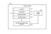
- FIG. 1is a diagram of an illustrative imaging system for optical and infrared imaging in accordance with an embodiment of the present invention.
- FIG. 2is a schematic side view of an illustrative camera module in accordance with an embodiment of the present invention.
- FIG. 3is a top view of an illustrative microelectromechanical systems device that may be used in an infrared and optical imaging system in accordance with an embodiment of the present invention.
- FIG. 4cross-sectional side view of an illustrative microelectromechanical systems element of a microelectromechanical systems device of the type shown in FIG. 3 showing how the microelectromechanical systems may rotate in response to incoming infrared light in accordance with an embodiment of the present invention.
- FIG. 5cross-sectional side view of an illustrative microelectromechanical systems element of a microelectromechanical systems device of the type shown in FIG. 3 showing how the microelectromechanical systems may actuate away from or towards an image sensor in response to incoming infrared light in accordance with an embodiment of the present invention.
- FIG. 6is a block diagram of a processor system that may include a camera module of the type shown in FIG. 2 in accordance with an embodiment of the present invention.
- Electronic devicessuch as digital cameras, computers, cellular telephones, and other electronic devices include image sensors that gather incoming light to capture an image.
- a microelectromechanical systems (MEMS) devicemay be mounted over the image sensor. Microelectromechanical systems elements in the MEMS device may change position due to absorption of infrared light.
- the image sensormay detect incoming infrared light by detecting the changes in position of the MEMS elements.
- a beam splittermay be included in the electronic device operable for switchably capturing visible light images through a lens and capturing images of the MEMS device for forming infrared images.
- the image sensorsmay include arrays of image pixels.
- the pixels in the image sensorsmay include photosensitive elements such as photodiodes that convert the incoming light into image signals.
- Image sensorsmay have any number of pixels (e.g., hundreds or thousands or more).
- a typical image sensormay, for example, have hundreds of thousands or millions of pixels (e.g., megapixels).
- Image sensorsmay include control circuitry such as circuitry for operating the image pixels and readout circuitry for reading out image signals corresponding to the electric charge generated by the photosensitive elements.
- the image pixelsmay be arranged in pixel rows and pixel columns.
- FIG. 1is a diagram of an illustrative imaging system such as an optical and infrared imaging system.
- System 10 of FIG. 1may be a portable electronic device such as a camera, a cellular telephone, a video camera, a computer, or other electronic device.
- System 10may include a camera module such as camera module 12 , a light source such as light source 22 , and processing circuitry such as storage and processing circuitry 18 .
- Storage and processing circuitry 18may be used to operate camera module 12 , to operate light source 22 , and/or to process image data such as infrared image data and optical image data from camera module 12 .
- camera module 12may include one or more image sensor such as image sensor 16 .
- Image sensor 16may include an array of image pixels such as complementary-metal-oxide-semiconductor (CMOS) image pixels, charged- coupled-device (CCD) image pixels or other image pixels.
- CMOScomplementary-metal-oxide-semiconductor
- CCDcharged- coupled-device
- Camera module 12may also include a microelectromechanical systems device such as MEMS array 13 .
- MEMS array 13may include an array of MEMS elements that change position and/or shape in response to absorption of infrared light.
- Image sensor 16may be configured to capture images of MEMS array 13 .
- Processing circuitry associated with image sensor 16 and/or storage and processing circuitry 18may be used to generate infrared images of a scene using the captured images of MEMS array 13 .
- camera module 12may include a light source such as light source 22 that illuminates MEMS array 13 .
- Light source 22may direct light toward a surface of MEMS array 13 . Infrared light may illuminate a first side of MEMS array 13 and light from light source 22 may illuminate an opposing side of MEMS array 13 .
- Image sensor 16may capture images of light from light source 22 that is reflected from the opposing side of MEMS array 13 .
- Light source 22may directly illuminate MEMS array 13 or one or more light redirecting structures such as one or more of lenses 14 and/or one or more of beam splitters 24 may direct light from light source 22 onto MEMS array 13 .
- Lenses 14may include one or more infrared focusing lenses and, if desired, one or more visible light focusing lenses.
- One or more infrared focusing lensesmay focus infrared light onto MEMS array 13 .
- Camera module 12may include one or more beam splitters 24 .
- Beam splitters 24may include a beam splitter that redirects light from light source 22 onto a surface of MEMS array 13 .
- Beam splitters 24may, if desired, include an additional beam splitter that redirects visible light from a scene onto image sensor 16 .
- One or more beam splittersmay be movable beam splitter that can be moved to switch camera module 12 between imaging modes of operation such as a visible light imaging mode to an infrared imaging mode.
- Processing circuitry 18may include one or more integrated circuits (e.g., image processing circuits, microprocessors, storage devices such as random-access memory and non-volatile memory, etc.) and may be implemented using components that are separate from camera module 12 and/or components that form part of camera module 12 (e.g., circuits that form part of an integrated circuit that includes image sensor 16 ).
- Optical images of MEMS array 13may be processed using processing circuitry 18 to form infrared images of a scene.
- Processed datamay, if desired, be provided to external equipment (e.g., a computer or other device) using wired and/or wireless communications paths coupled to processing circuitry 18 .
- camera module 12may include an infrared lens such as infrared (IR) lens 30 .
- IR lens 30may focus incoming infrared light 52 onto surface 34 of MEMS array 13 (as indicated by arrows 40 ).
- thisis merely illustrative.
- other optical collection and focusing structuressuch as a Cassegrain optical system may be used to focus infrared light onto surface 34 of MEMS array 13 , thereby creating a infrared image on surface 34 of MEMS array 13 .
- Light source 22may direct light such as visible light through a lens such as lens 36 onto a beam splitter such as beam splitter 24 .
- Beam splitter 24may then redirect the light from light source 22 onto an opposing surface such as surface 35 of MEMS array 13 (as indicated by arrows 44 ).
- the light that is redirected onto surface 35 of MEMS array 13may then reflect from surface 35 and pass through beam splitter 24 and onto image sensor 16 (as indicated by arrow 46 ).
- Image sensor 16may be configured to capture images of surface 35 using the light that has been reflected from surface 35 of MEMS array 13 through beam splitter 24 .
- MEMS elements in MEMS array 13may be configured to absorb infrared light 52 that has been focused by lens 30 and to change position and/or shape due to the absorption of the infrared light.
- Infrared images of a scenemay be generated (e.g., using processing circuitry 18 ) using the captured images of MEMS array 13 by detecting the changes in position and/or shape of the MEMS elements in the captured images.
- interfering structures 38may be included in the path along which light travels from surface 35 of MEMS array 13 to image sensor 16 .
- structures 38may include a Fabry-Perot etalon or other light phase imaging or interferometry structures.
- image sensor 16may capture phase images or interferometric images that contain information about slight movements of the MEMS elements in MEMS array 13 . In this way, shifts in position of the MEMS elements to within fractions of a wavelength of the visible illumination light being used can be measured, thereby providing a highly sensitive measurement of the amount of infrared light that has been absorbed by each MEMS element.
- camera module 12may be provided without any additional structures 38 .
- FIG. 2The arrangement of FIG. 2 in which beam splitter 24 is used to direct light form light source 22 onto MEMS array 13 is merely illustrative. If desired, other arrangements may be used. For example, lenses may be arranged in camera module 12 to illuminate MEMS array 13 at an angle from perpendicular and, if desired, a field lens may be used to direct reflected light from MEMS array 13 onto image sensor 16 . As another example, MEMS elements in MEMS array 13 may have curved optical surfaces. In this type of configuration, camera module 12 may be provided without a lens that focuses light from MEMS elements onto image sensor 16 .
- the reflected light from the MEMS elementsmay be arranged to move across multiple image pixels on image sensor 16 when the MEMS elements absorb incident infrared light.
- processing circuitry 18may be used to perform super resolution imaging operations in order to extract positioning data that describes the positions of the MEMS elements from captured images of MEMS array 13 . In this way, the measuring accuracy of the MEMS elements positions and shapes may be increased, thereby increasing the accuracy of the intensity measurement of the incident infrared photons.
- optical (visible light) imaging componentsmay also be included in camera module 12 .
- One or more optical lensessuch as lens 32 may be used to focus visible light 50 for camera module 12 .
- Lens 32may focus visible light 50 onto a mirror or a beam splitter such as beam splitter 24 ′ (as indicated by dashed arrows 42 ).
- beam splitter 24 ′may redirect visible light onto beam splitter 24 (as indicated by dashed arrow 48 ).
- the visible light that has been redirected onto beam splitter 24may then be redirected onto image sensor 16 .
- Image sensor 16may capture an image of a scene using image pixels on image sensor 16 to convert visible light from beam splitter 24 into electric charges and generate image signals based on those electric charges.
- beam splitter 24 ′may be a movable beam splitter that can be moved and or rotated (e.g., in directions 49 and 51 ). In this way, visible light may be switchably directed onto image sensor 16 or away from image sensor 16 depending on the mode of operation of camera module 12 .
- a visible light imaging modelight source 22 may be turned off and beam splitter 24 ′ (and beam splitter 24 ) may direct visible light onto image sensor 16 .
- an infrared imaging modelight source 22 may be turned on and beam splitter 24 ′ may be moved (e.g. , in direction 49 ) so that visible light from lens 32 is directed away from image sensor 16 and light from light source 22 that has reflected off of MEMS array 13 is imaged by image sensor 16 .
- Beam splitters 24 and 24 ′may therefore switchably direct light from optical lens 32 and the MEMS array 13 onto image sensor 16 .
- FIG. 3is a top view of a portion of surface 34 of MEMS array 13 .
- MEMS array 13may include a plurality of MEMS elements 54 .
- MEMS elements 54may be formed form metal or other materials and may have infrared absorbing material such as infrared absorbing material 56 on a surface of the metal.
- IR absorbing material 56is patterned on the surface of metal support structures.
- MEMS elements 54may move, actuate, bend, flex, rotate, or otherwise change their position and/or shape in response to temperature changes or charge generation generated by infrared light that has been absorbed by material 56 on each element 54 . Differences in the amount of change in shape and/or position from element to element may be used to map the distribution of infrared light that has fallen on MEMS array 13 .
- Material 56 on MEMS elements 54may be designed to absorb thermal radiation in a selected wavelength band region, such as from 8 microns to 15 microns in wavelength (as an example).
- FIGS. 4 and 5show two exemplary embodiments of MEMS elements 54 .
- MEMS elements 54may be formed from a first metal layer such as metal layer 62 formed on a second metal layer such as metal layer 60 .
- Metal layer 60may have a coefficient of thermal expansion that is different from the coefficient of thermal expansion of metal layer 62 .
- a patterned layer of IR absorbing material 56may be formed on metal layer 62 .
- IR absorbing material 56may absorb incoming infrared photons 52 within the selected wavelength region and convert the absorbed photons into internal heat. The heat generated in material 56 may be transferred to layers 62 and 60 . Because layers 60 and 62 have different coefficients of thermal expansion, this heat may cause MEMS element 54 to bend or flex in a given direction by an amount proportional to the number of IR photons 52 that element has absorbed.
- one edge of MEMS element 54is attached to support structure 68 so that MEMS element 54 will rotate as indicated by arrows 70 when more or less infrared light 52 is absorbed by material 56 .
- the amount of rotation of element 54may be detected using visible light 66 (e.g., from light source 22 ) that reflects from interior surface 34 of layer 60 and onto image sensor 16 . Because each MEMS element 54 will receive an amount of infrared light that depends on the amount of infrared light at a corresponding location in a scene, the measured deflection of MEMS elements 54 can be converted into an infrared image (sometimes referred to as a heat image) of the scene.
- MEMS element 54is configured as an electrical field MEMS.
- MEMS element 54is formed from a single metal layer such as layer 62 with a patterned coating of IR absorbing material 56 on the scene-facing side of MEMS element 54 .
- MEMS element 54may include a stationary electrode such as electrode 78 mounted at a distance from layer 62 . Electrical charges may be formed on metal layer 62 and electrode 78 .
- material 56may be formed from a material that converts incoming infrared photons 52 into electrons, thereby increasing the charge on layer 62 proportionally to the amount of infrared light 52 received.
- the increased charge on layer 62may generate a force on layer 62 due to the charges on electrode 78 .
- elements 54may therefore bend, flex, actuate, move, rotate, or otherwise change position and/or shape based on the amount of infrared light 52 that has been absorbed.
- electrode 78may be used to drive layer 62 into oscillation such that layer 62 moves in a regular cycle away from and toward stationary electrode 78 as indicated by arrows 72 .
- the motion of metal layer 62will alter its frequency and magnitude of oscillation as additional charges are built up through the conversion of IR photons 52 into additional electrical charge.
- This mode of operationmay allow MEMS elements 54 to be charged to preset levels for dynamic range control, damping of oscillation and discharge between frames, if desired.
- MEMS element 54may be reflective so that visible light illuminating surface 34 is reflected from the MEMS element 54 towards the detection surface of image sensor 16 .
- MEMS element 54can have a flat surface as shown in FIG. 4 or can be formed to have a concave surface as shown in FIG. 5 so that reflected portions of light 66 are focused into a small area on image sensor 16 .
- metal layer 62is supported on multiple corners by support structure 74 .
- Structures 74may be rigid structures so that metal layer 62 bends into a curved shape due to forces resulting from the increased charge on layer 62 .
- layer 62may be secured at one corner, at two corners, at three corners, along one edge, along two edges, along three edges or in any suitable configuration so that layer 62 changes shape and/or position in response to infrared light 52 that has been absorbed by material 56 .
- FIG. 6shows in simplified form a typical processor system 300 , such as a digital camera, which includes an imaging device such as imaging device 200 .
- Imaging device 200may, for example, be an optical and infrared imaging system such as camera module 12 .
- Processor system 300is exemplary of a system having digital circuits that could include imaging device 200 . Without being limiting, such a system could include a computer system, still or video camera system, scanner, machine vision, vehicle navigation, video phone, surveillance system, auto focus system, star tracker system, motion detection system, image stabilization system, and other systems employing an imaging device.
- Processor system 300may include a lens such as lens 396 for focusing an image onto a pixel array such as pixel array 201 when shutter release button 397 is pressed.
- Processor system 300may include a central processing unit such as central processing unit (CPU) 395 .
- CPU 395may be a microprocessor that controls camera functions and one or more image flow functions and communicates with one or more input/output (I/O) devices 391 over a bus such as bus 393 .
- Imaging device 200may also communicate with CPU 395 over bus 393 .
- System 300may include random access memory (RAM) 392 and removable memory 394 .
- Removable memory 394may include flash memory that communicates with CPU 395 over bus 393 .
- Imaging device 200may be combined with CPU 395 , with or without memory storage, on a single integrated circuit or on a different chip.
- bus 393is illustrated as a single bus, it may be one or more buses or bridges or other communication paths used to interconnect the system components.
- optical and infrared imaging systemmay be used separately as an optical imaging system and as an infrared imaging system, or may be switched between optical and infrared imaging modes of operations.
- the systemmay include an image sensor such as a CMOS image sensor for capturing images using visible light.
- Optical imagesmay be captured using an optical lens and one or more mirrors and/or beam splitters to direct visible light on the image sensor.
- Infrared imagesmay be generated using a microelectromechanical systems (MEMS) array.
- MEMS arraymay be mounted in front of the image sensor.
- the MEMS arraymay include an array of MEMS elements that absorb infrared light and change position and/or shape in response to the absorbed infrared light.
- Each MEMS elementmay include infrared absorbing material on a metal structure. The infrared absorbing material may generate heat and/or electric charge in response to the absorbed infrared light.
- An infrared lensmay be configured to focus an infrared image of a scene onto a first surface of the MEMS array.
- a light sourcemay be used to illuminate an opposing surface of the MEMS array.
- the image sensormay be configured to capture images of the illuminated opposing surface of the MEMS array.
- Processing circuitrymay be provided that generates an infrared image of a scene using the visible light images of the MEMS array.
Landscapes
- Engineering & Computer Science (AREA)
- Multimedia (AREA)
- Signal Processing (AREA)
- Physics & Mathematics (AREA)
- Human Computer Interaction (AREA)
- Chemical & Material Sciences (AREA)
- Computer Hardware Design (AREA)
- Microelectronics & Electronic Packaging (AREA)
- Analytical Chemistry (AREA)
- General Engineering & Computer Science (AREA)
- Theoretical Computer Science (AREA)
- General Physics & Mathematics (AREA)
- Spectroscopy & Molecular Physics (AREA)
- Transforming Light Signals Into Electric Signals (AREA)
- Studio Devices (AREA)
- Optics & Photonics (AREA)
Abstract
Description
- This application claims the benefit of provisional patent application No. 61/619,364, filed Apr. 2, 2012, which is hereby incorporated by reference herein in its entirety.
- This relates generally to imaging systems, and more particularly, to infrared imaging systems.
- Conventional silicon imaging devices have a bandgap limit near a wavelength of one micron, above which they lose their ability to generate electrons from interactions with photons. These conventional devices therefore have limited capability of detecting infrared radiation from the bandgap limit through the infrared spectral region.
- This has resulted in the development of two different specialized infrared imaging technologies, exotic semiconductors such as Mercury Cadmium Telluride (HgCdTe) semiconductors, Indium Antimonide semiconductors, etc. or microelectromechanical systems (MEMS) based bolometers. MEMS based bolometers typically include metal layers with differing coefficients of expansion that flex when infrared radiation is absorbed. This flexing changes the capacitance of the MEMS devices thereby allowing detection of infrared radiation by detecting the changes in capacitance.
- Exotic semiconductors can have a prohibitively high cost for mass production of infrared imaging systems and cannot capture visible light images. MEMS- based bolometer devices also cannot capture visible light images.
- It would therefore be desirable to be able to provide improved infrared imaging systems.
FIG. 1 is a diagram of an illustrative imaging system for optical and infrared imaging in accordance with an embodiment of the present invention.FIG. 2 is a schematic side view of an illustrative camera module in accordance with an embodiment of the present invention.FIG. 3 is a top view of an illustrative microelectromechanical systems device that may be used in an infrared and optical imaging system in accordance with an embodiment of the present invention.FIG. 4 cross-sectional side view of an illustrative microelectromechanical systems element of a microelectromechanical systems device of the type shown inFIG. 3 showing how the microelectromechanical systems may rotate in response to incoming infrared light in accordance with an embodiment of the present invention.FIG. 5 cross-sectional side view of an illustrative microelectromechanical systems element of a microelectromechanical systems device of the type shown inFIG. 3 showing how the microelectromechanical systems may actuate away from or towards an image sensor in response to incoming infrared light in accordance with an embodiment of the present invention.FIG. 6 is a block diagram of a processor system that may include a camera module of the type shown inFIG. 2 in accordance with an embodiment of the present invention.- Electronic devices such as digital cameras, computers, cellular telephones, and other electronic devices include image sensors that gather incoming light to capture an image. A microelectromechanical systems (MEMS) device may be mounted over the image sensor. Microelectromechanical systems elements in the MEMS device may change position due to absorption of infrared light. The image sensor may detect incoming infrared light by detecting the changes in position of the MEMS elements. A beam splitter may be included in the electronic device operable for switchably capturing visible light images through a lens and capturing images of the MEMS device for forming infrared images.
- The image sensors may include arrays of image pixels. The pixels in the image sensors may include photosensitive elements such as photodiodes that convert the incoming light into image signals. Image sensors may have any number of pixels (e.g., hundreds or thousands or more). A typical image sensor may, for example, have hundreds of thousands or millions of pixels (e.g., megapixels). Image sensors may include control circuitry such as circuitry for operating the image pixels and readout circuitry for reading out image signals corresponding to the electric charge generated by the photosensitive elements. The image pixels may be arranged in pixel rows and pixel columns.
FIG. 1 is a diagram of an illustrative imaging system such as an optical and infrared imaging system.System 10 ofFIG. 1 may be a portable electronic device such as a camera, a cellular telephone, a video camera, a computer, or other electronic device.System 10 may include a camera module such ascamera module 12, a light source such aslight source 22, and processing circuitry such as storage andprocessing circuitry 18. Storage andprocessing circuitry 18 may be used to operatecamera module 12, to operatelight source 22, and/or to process image data such as infrared image data and optical image data fromcamera module 12.- As shown in
FIG. 1 ,camera module 12 may include one or more image sensor such asimage sensor 16.Image sensor 16 may include an array of image pixels such as complementary-metal-oxide-semiconductor (CMOS) image pixels, charged- coupled-device (CCD) image pixels or other image pixels. Camera module 12 may also include a microelectromechanical systems device such asMEMS array 13.MEMS array 13 may include an array of MEMS elements that change position and/or shape in response to absorption of infrared light.Image sensor 16 may be configured to capture images ofMEMS array 13. Processing circuitry associated withimage sensor 16 and/or storage andprocessing circuitry 18 may be used to generate infrared images of a scene using the captured images ofMEMS array 13.- If desired,
camera module 12 may include a light source such aslight source 22 that illuminatesMEMS array 13.Light source 22 may direct light toward a surface ofMEMS array 13. Infrared light may illuminate a first side ofMEMS array 13 and light fromlight source 22 may illuminate an opposing side ofMEMS array 13.Image sensor 16 may capture images of light fromlight source 22 that is reflected from the opposing side ofMEMS array 13.Light source 22 may directly illuminateMEMS array 13 or one or more light redirecting structures such as one or more oflenses 14 and/or one or more ofbeam splitters 24 may direct light fromlight source 22 ontoMEMS array 13. Lenses 14 may include one or more infrared focusing lenses and, if desired, one or more visible light focusing lenses. One or more infrared focusing lenses may focus infrared light ontoMEMS array 13.Camera module 12 may include one ormore beam splitters 24.Beam splitters 24 may include a beam splitter that redirects light fromlight source 22 onto a surface ofMEMS array 13.Beam splitters 24 may, if desired, include an additional beam splitter that redirects visible light from a scene ontoimage sensor 16. One or more beam splitters may be movable beam splitter that can be moved to switchcamera module 12 between imaging modes of operation such as a visible light imaging mode to an infrared imaging mode.Processing circuitry 18 may include one or more integrated circuits (e.g., image processing circuits, microprocessors, storage devices such as random-access memory and non-volatile memory, etc.) and may be implemented using components that are separate fromcamera module 12 and/or components that form part of camera module12 (e.g., circuits that form part of an integrated circuit that includes image sensor16). Optical images ofMEMS array 13 may be processed usingprocessing circuitry 18 to form infrared images of a scene. Processed data may, if desired, be provided to external equipment (e.g., a computer or other device) using wired and/or wireless communications paths coupled to processingcircuitry 18.- As shown in
FIG. 2 ,camera module 12 may include an infrared lens such as infrared (IR)lens 30.IR lens 30 may focus incoming infrared light52 ontosurface 34 of MEMS array13 (as indicated by arrows40). However, this is merely illustrative. If desired, other optical collection and focusing structures such as a Cassegrain optical system may be used to focus infrared light ontosurface 34 ofMEMS array 13, thereby creating a infrared image onsurface 34 ofMEMS array 13. - Light source22 (e.g., a light-emitting diode or other light source) may direct light such as visible light through a lens such as
lens 36 onto a beam splitter such asbeam splitter 24.Beam splitter 24 may then redirect the light fromlight source 22 onto an opposing surface such assurface 35 of MEMS array13 (as indicated by arrows44). The light that is redirected ontosurface 35 ofMEMS array 13 may then reflect fromsurface 35 and pass throughbeam splitter 24 and onto image sensor16 (as indicated by arrow46).Image sensor 16 may be configured to capture images ofsurface 35 using the light that has been reflected fromsurface 35 ofMEMS array 13 throughbeam splitter 24. MEMS elements inMEMS array 13 may be configured to absorb infrared light52 that has been focused bylens 30 and to change position and/or shape due to the absorption of the infrared light. - Infrared images of a scene may be generated (e.g., using processing circuitry18) using the captured images of
MEMS array 13 by detecting the changes in position and/or shape of the MEMS elements in the captured images. - If desired, additional structures such as
interfering structures 38 may be included in the path along which light travels fromsurface 35 ofMEMS array 13 toimage sensor 16. For example,structures 38 may include a Fabry-Perot etalon or other light phase imaging or interferometry structures. In this type of configuration,image sensor 16 may capture phase images or interferometric images that contain information about slight movements of the MEMS elements inMEMS array 13. In this way, shifts in position of the MEMS elements to within fractions of a wavelength of the visible illumination light being used can be measured, thereby providing a highly sensitive measurement of the amount of infrared light that has been absorbed by each MEMS element. However, this is merely illustrative. If desired,camera module 12 may be provided without anyadditional structures 38. - The arrangement of
FIG. 2 in whichbeam splitter 24 is used to direct lightform light source 22 ontoMEMS array 13 is merely illustrative. If desired, other arrangements may be used. For example, lenses may be arranged incamera module 12 to illuminateMEMS array 13 at an angle from perpendicular and, if desired, a field lens may be used to direct reflected light fromMEMS array 13 ontoimage sensor 16. As another example, MEMS elements inMEMS array 13 may have curved optical surfaces. In this type of configuration,camera module 12 may be provided without a lens that focuses light from MEMS elements ontoimage sensor 16. - To further enhance infrared imaging performance, the reflected light from the MEMS elements may be arranged to move across multiple image pixels on
image sensor 16 when the MEMS elements absorb incident infrared light. In this type of arrangement, processingcircuitry 18 may be used to perform super resolution imaging operations in order to extract positioning data that describes the positions of the MEMS elements from captured images ofMEMS array 13. In this way, the measuring accuracy of the MEMS elements positions and shapes may be increased, thereby increasing the accuracy of the intensity measurement of the incident infrared photons. - If desired, optical (visible light) imaging components may also be included in
camera module 12. One or more optical lenses such aslens 32 may be used to focusvisible light 50 forcamera module 12.Lens 32 may focusvisible light 50 onto a mirror or a beam splitter such asbeam splitter 24′ (as indicated by dashed arrows42). In an optical imaging mode,beam splitter 24′ may redirect visible light onto beam splitter24 (as indicated by dashed arrow48). The visible light that has been redirected ontobeam splitter 24 may then be redirected ontoimage sensor 16.Image sensor 16 may capture an image of a scene using image pixels onimage sensor 16 to convert visible light frombeam splitter 24 into electric charges and generate image signals based on those electric charges. - If desired,
beam splitter 24′ may be a movable beam splitter that can be moved and or rotated (e.g., indirections 49 and51). In this way, visible light may be switchably directed ontoimage sensor 16 or away fromimage sensor 16 depending on the mode of operation ofcamera module 12. In a visible light imaging mode,light source 22 may be turned off andbeam splitter 24′ (and beam splitter24) may direct visible light ontoimage sensor 16. In an infrared imaging mode,light source 22 may be turned on andbeam splitter 24′ may be moved (e.g. , in direction49) so that visible light fromlens 32 is directed away fromimage sensor 16 and light fromlight source 22 that has reflected off ofMEMS array 13 is imaged byimage sensor 16.Beam splitters optical lens 32 and theMEMS array 13 ontoimage sensor 16. FIG. 3 is a top view of a portion ofsurface 34 ofMEMS array 13. As shown inFIG. 3 ,MEMS array 13 may include a plurality ofMEMS elements 54.MEMS elements 54 may be formed form metal or other materials and may have infrared absorbing material such as infrared absorbingmaterial 56 on a surface of the metal. In the example ofFIG. 3 ,IR absorbing material 56 is patterned on the surface of metal support structures.MEMS elements 54 may move, actuate, bend, flex, rotate, or otherwise change their position and/or shape in response to temperature changes or charge generation generated by infrared light that has been absorbed bymaterial 56 on eachelement 54. Differences in the amount of change in shape and/or position from element to element may be used to map the distribution of infrared light that has fallen onMEMS array 13.Material 56 onMEMS elements 54 may be designed to absorb thermal radiation in a selected wavelength band region, such as from 8 microns to 15 microns in wavelength (as an example).FIGS. 4 and 5 show two exemplary embodiments ofMEMS elements 54.- As shown in
FIG. 4 ,MEMS elements 54 may be formed from a first metal layer such asmetal layer 62 formed on a second metal layer such asmetal layer 60.Metal layer 60 may have a coefficient of thermal expansion that is different from the coefficient of thermal expansion ofmetal layer 62. A patterned layer ofIR absorbing material 56 may be formed onmetal layer 62.IR absorbing material 56 may absorb incominginfrared photons 52 within the selected wavelength region and convert the absorbed photons into internal heat. The heat generated inmaterial 56 may be transferred tolayers layers MEMS element 54 to bend or flex in a given direction by an amount proportional to the number ofIR photons 52 that element has absorbed. - In the example of
FIG. 4 , one edge ofMEMS element 54 is attached to supportstructure 68 so thatMEMS element 54 will rotate as indicated byarrows 70 when more or lessinfrared light 52 is absorbed bymaterial 56. The amount of rotation ofelement 54 may be detected using visible light66 (e.g., from light source22) that reflects frominterior surface 34 oflayer 60 and ontoimage sensor 16. Because eachMEMS element 54 will receive an amount of infrared light that depends on the amount of infrared light at a corresponding location in a scene, the measured deflection ofMEMS elements 54 can be converted into an infrared image (sometimes referred to as a heat image) of the scene. - In the example of
FIG. 5 ,MEMS element 54 is configured as an electrical field MEMS. In this type of configuration,MEMS element 54 is formed from a single metal layer such aslayer 62 with a patterned coating ofIR absorbing material 56 on the scene-facing side ofMEMS element 54.MEMS element 54 may include a stationary electrode such aselectrode 78 mounted at a distance fromlayer 62. Electrical charges may be formed onmetal layer 62 andelectrode 78. In this type of configuration,material 56 may be formed from a material that converts incominginfrared photons 52 into electrons, thereby increasing the charge onlayer 62 proportionally to the amount of infrared light52 received. The increased charge onlayer 62 may generate a force onlayer 62 due to the charges onelectrode 78. In response to this force,elements 54 may therefore bend, flex, actuate, move, rotate, or otherwise change position and/or shape based on the amount of infrared light52 that has been absorbed. - If desired,
electrode 78 may be used to drivelayer 62 into oscillation such thatlayer 62 moves in a regular cycle away from and towardstationary electrode 78 as indicated byarrows 72. In this type of configuration, the motion ofmetal layer 62 will alter its frequency and magnitude of oscillation as additional charges are built up through the conversion ofIR photons 52 into additional electrical charge. This mode of operation may allowMEMS elements 54 to be charged to preset levels for dynamic range control, damping of oscillation and discharge between frames, if desired. Surface 34 of MEMS element54 (i.e., the surface facing image sensor16) may be reflective so that visiblelight illuminating surface 34 is reflected from theMEMS element 54 towards the detection surface ofimage sensor 16.MEMS element 54 can have a flat surface as shown inFIG. 4 or can be formed to have a concave surface as shown inFIG. 5 so that reflected portions of light66 are focused into a small area onimage sensor 16.- In the example of
FIG. 5 ,metal layer 62 is supported on multiple corners bysupport structure 74.Structures 74 may be rigid structures so thatmetal layer 62 bends into a curved shape due to forces resulting from the increased charge onlayer 62. However, this is merely illustrative. If desired,layer 62 may be secured at one corner, at two corners, at three corners, along one edge, along two edges, along three edges or in any suitable configuration so thatlayer 62 changes shape and/or position in response to infrared light52 that has been absorbed bymaterial 56. FIG. 6 shows in simplified form atypical processor system 300, such as a digital camera, which includes an imaging device such asimaging device 200.Imaging device 200 may, for example, be an optical and infrared imaging system such ascamera module 12.Processor system 300 is exemplary of a system having digital circuits that could includeimaging device 200. Without being limiting, such a system could include a computer system, still or video camera system, scanner, machine vision, vehicle navigation, video phone, surveillance system, auto focus system, star tracker system, motion detection system, image stabilization system, and other systems employing an imaging device.Processor system 300, which may be a digital still or video camera system, may include a lens such aslens 396 for focusing an image onto a pixel array such as pixel array201 whenshutter release button 397 is pressed.Processor system 300 may include a central processing unit such as central processing unit (CPU)395.CPU 395 may be a microprocessor that controls camera functions and one or more image flow functions and communicates with one or more input/output (I/O)devices 391 over a bus such asbus 393.Imaging device 200 may also communicate withCPU 395 overbus 393.System 300 may include random access memory (RAM)392 andremovable memory 394.Removable memory 394 may include flash memory that communicates withCPU 395 overbus 393.Imaging device 200 may be combined withCPU 395, with or without memory storage, on a single integrated circuit or on a different chip. Althoughbus 393 is illustrated as a single bus, it may be one or more buses or bridges or other communication paths used to interconnect the system components.- Various embodiments have been described illustrating an optical and infrared imaging system. The optical and infrared imaging system may be used separately as an optical imaging system and as an infrared imaging system, or may be switched between optical and infrared imaging modes of operations.
- The system may include an image sensor such as a CMOS image sensor for capturing images using visible light. Optical images may be captured using an optical lens and one or more mirrors and/or beam splitters to direct visible light on the image sensor. Infrared images may be generated using a microelectromechanical systems (MEMS) array. The MEMS array may be mounted in front of the image sensor. The MEMS array may include an array of MEMS elements that absorb infrared light and change position and/or shape in response to the absorbed infrared light. Each MEMS element may include infrared absorbing material on a metal structure. The infrared absorbing material may generate heat and/or electric charge in response to the absorbed infrared light.
- An infrared lens may be configured to focus an infrared image of a scene onto a first surface of the MEMS array. A light source may be used to illuminate an opposing surface of the MEMS array. The image sensor may be configured to capture images of the illuminated opposing surface of the MEMS array. Processing circuitry may be provided that generates an infrared image of a scene using the visible light images of the MEMS array.
- The foregoing is merely illustrative of the principles of this invention which can be practiced in other embodiments.
Claims (20)
Priority Applications (1)
| Application Number | Priority Date | Filing Date | Title |
|---|---|---|---|
| US13/854,834US9440844B2 (en) | 2012-04-02 | 2013-04-01 | Optical and infrared imaging system |
Applications Claiming Priority (2)
| Application Number | Priority Date | Filing Date | Title |
|---|---|---|---|
| US201261619364P | 2012-04-02 | 2012-04-02 | |
| US13/854,834US9440844B2 (en) | 2012-04-02 | 2013-04-01 | Optical and infrared imaging system |
Publications (2)
| Publication Number | Publication Date |
|---|---|
| US20150187828A1true US20150187828A1 (en) | 2015-07-02 |
| US9440844B2 US9440844B2 (en) | 2016-09-13 |
Family
ID=53482751
Family Applications (1)
| Application Number | Title | Priority Date | Filing Date |
|---|---|---|---|
| US13/854,834Expired - Fee RelatedUS9440844B2 (en) | 2012-04-02 | 2013-04-01 | Optical and infrared imaging system |
Country Status (1)
| Country | Link |
|---|---|
| US (1) | US9440844B2 (en) |
Cited By (6)
| Publication number | Priority date | Publication date | Assignee | Title |
|---|---|---|---|---|
| US20130279744A1 (en)* | 2012-04-23 | 2013-10-24 | Apple Inc. | Systems and methods for controlling output of content based on human recognition data detection |
| US20180047643A1 (en)* | 2016-08-11 | 2018-02-15 | Applied Materials, Inc. | Thermal Profile Monitoring Wafer And Methods Of Monitoring Temperature |
| US10057510B2 (en) | 2014-06-20 | 2018-08-21 | Rambus Inc. | Systems and methods for enhanced infrared imaging |
| WO2020219039A1 (en)* | 2019-04-24 | 2020-10-29 | Hewlett-Packard Development Company, L.P. | Displays with pixels coupled by beam splitters |
| EP3674742A4 (en)* | 2017-08-25 | 2021-01-27 | Kyocera Corporation | Electromagnetic wave detection device, program, and electromagnetic wave detection system |
| WO2022179272A1 (en)* | 2021-02-26 | 2022-09-01 | Oppo广东移动通信有限公司 | Optical imaging system, camera, and electronic device |
Families Citing this family (5)
| Publication number | Priority date | Publication date | Assignee | Title |
|---|---|---|---|---|
| US9730649B1 (en) | 2016-09-13 | 2017-08-15 | Open Water Internet Inc. | Optical imaging of diffuse medium |
| US10778912B2 (en) | 2018-03-31 | 2020-09-15 | Open Water Internet Inc. | System and device for optical transformation |
| US10506181B2 (en) | 2018-03-31 | 2019-12-10 | Open Water Internet Inc. | Device for optical imaging |
| US10778911B2 (en) | 2018-03-31 | 2020-09-15 | Open Water Internet Inc. | Optical transformation device for imaging |
| CN110139015A (en)* | 2019-06-13 | 2019-08-16 | 深圳惠聪科技有限公司 | A kind of electron telescope |
Citations (5)
| Publication number | Priority date | Publication date | Assignee | Title |
|---|---|---|---|---|
| US20100038542A1 (en)* | 2008-08-15 | 2010-02-18 | Sionyx, Inc. | Wideband Semiconducting Light Detector |
| US20100127172A1 (en)* | 2008-11-21 | 2010-05-27 | Nikoobakht Babak | Use of noble metal nanoparticles as light absorbers and heat generators in thermal photodetectors, sensors and microelecromechanical devices |
| US20110115919A1 (en)* | 2009-03-05 | 2011-05-19 | Masao Hiramoto | Solid-state imaging element and imaging device |
| US20110316982A1 (en)* | 2010-06-10 | 2011-12-29 | Arnold & Richter Cine Technik Gmbh & Co. | Camera objective and camera system |
| US20140078509A1 (en)* | 2011-05-02 | 2014-03-20 | Green Vision Systems Ltd. | Microelectromechanical system (mems) and (mem) optical interferometer for hyper-spectral imaging and analysis |
Family Cites Families (3)
| Publication number | Priority date | Publication date | Assignee | Title |
|---|---|---|---|---|
| US6952530B2 (en) | 2003-12-19 | 2005-10-04 | The Aerospace Corporation | Integrated glass ceramic systems |
| BRPI0921770A2 (en) | 2008-11-04 | 2016-01-05 | Univ Rice William M | image mapping spectrometers |
| GB201110159D0 (en) | 2011-06-16 | 2011-07-27 | Light Blue Optics Ltd | Touch sensitive display devices |
- 2013
- 2013-04-01USUS13/854,834patent/US9440844B2/ennot_activeExpired - Fee Related
Patent Citations (5)
| Publication number | Priority date | Publication date | Assignee | Title |
|---|---|---|---|---|
| US20100038542A1 (en)* | 2008-08-15 | 2010-02-18 | Sionyx, Inc. | Wideband Semiconducting Light Detector |
| US20100127172A1 (en)* | 2008-11-21 | 2010-05-27 | Nikoobakht Babak | Use of noble metal nanoparticles as light absorbers and heat generators in thermal photodetectors, sensors and microelecromechanical devices |
| US20110115919A1 (en)* | 2009-03-05 | 2011-05-19 | Masao Hiramoto | Solid-state imaging element and imaging device |
| US20110316982A1 (en)* | 2010-06-10 | 2011-12-29 | Arnold & Richter Cine Technik Gmbh & Co. | Camera objective and camera system |
| US20140078509A1 (en)* | 2011-05-02 | 2014-03-20 | Green Vision Systems Ltd. | Microelectromechanical system (mems) and (mem) optical interferometer for hyper-spectral imaging and analysis |
Non-Patent Citations (3)
| Title |
|---|
| "Optomechanical Uncooled Infrared Imaging System:Design, Microfabrication, and Performance", Journal of MICROELECTROMECHANICAL SYSTEMS, VOL. 11, NO. 2, APRIL 2002, pp. 136 - 146, to Zhao et al.* |
| "Polymer-Ceramic MEMS Bimorphs as Thermal Infrared Sensors", p. 1-94, UC Berkley Electronic Theses and Disserations, to Warren (2010)* |
| Thermopile infrared sensor with precisely patterned high-temperature resistant black absorber layer", SENSOR + TEST Conference 2009, p. 197 - 202 to Ihring et al.* |
Cited By (13)
| Publication number | Priority date | Publication date | Assignee | Title |
|---|---|---|---|---|
| US10360360B2 (en)* | 2012-04-23 | 2019-07-23 | Apple Inc. | Systems and methods for controlling output of content based on human recognition data detection |
| US9633186B2 (en)* | 2012-04-23 | 2017-04-25 | Apple Inc. | Systems and methods for controlling output of content based on human recognition data detection |
| US20170277875A1 (en)* | 2012-04-23 | 2017-09-28 | Apple Inc. | Systems and methods for controlling output of content based on human recognition data detection |
| US20130279744A1 (en)* | 2012-04-23 | 2013-10-24 | Apple Inc. | Systems and methods for controlling output of content based on human recognition data detection |
| US10057510B2 (en) | 2014-06-20 | 2018-08-21 | Rambus Inc. | Systems and methods for enhanced infrared imaging |
| US10651095B2 (en)* | 2016-08-11 | 2020-05-12 | Applied Materials, Inc. | Thermal profile monitoring wafer and methods of monitoring temperature |
| US20180047643A1 (en)* | 2016-08-11 | 2018-02-15 | Applied Materials, Inc. | Thermal Profile Monitoring Wafer And Methods Of Monitoring Temperature |
| TWI744374B (en)* | 2016-08-11 | 2021-11-01 | 美商應用材料股份有限公司 | Thermal profile monitoring wafer and methods of monitoring temperature |
| US11515218B2 (en)* | 2016-08-11 | 2022-11-29 | Applied Materials, Inc. | Thermal profile monitoring wafer and methods of monitoring temperature |
| EP3674742A4 (en)* | 2017-08-25 | 2021-01-27 | Kyocera Corporation | Electromagnetic wave detection device, program, and electromagnetic wave detection system |
| WO2020219039A1 (en)* | 2019-04-24 | 2020-10-29 | Hewlett-Packard Development Company, L.P. | Displays with pixels coupled by beam splitters |
| US11551592B2 (en) | 2019-04-24 | 2023-01-10 | Hewlett-Packard Development Company, L.P. | Displays with pixels coupled by beam splitters |
| WO2022179272A1 (en)* | 2021-02-26 | 2022-09-01 | Oppo广东移动通信有限公司 | Optical imaging system, camera, and electronic device |
Also Published As
| Publication number | Publication date |
|---|---|
| US9440844B2 (en) | 2016-09-13 |
Similar Documents
| Publication | Publication Date | Title |
|---|---|---|
| US9440844B2 (en) | Optical and infrared imaging system | |
| Bhan et al. | Recent infrared detector technologies, applications, trends and development of HgCdTe based cooled infrared focal plane arrays and their characterization | |
| US10110833B2 (en) | Hybrid infrared sensor array having heterogeneous infrared sensors | |
| EP2923187B1 (en) | Hybrid infrared sensor array having heterogeneous infrared sensors | |
| US8461530B2 (en) | Sensor array microchip | |
| KR100924179B1 (en) | Method and apparatus for controlling a lens, and camera module incorporating same | |
| US9247131B2 (en) | Alignment of visible light sources based on thermal images | |
| US20140139643A1 (en) | Imager with array of multiple infrared imaging modules | |
| US11012635B2 (en) | Optical device including pinhole array aperture and related methods | |
| US9235023B2 (en) | Variable lens sleeve spacer | |
| US9729806B2 (en) | Imaging systems with phase detection pixels | |
| US9945718B2 (en) | Image sensors with multi-functional pixel clusters | |
| KR102128467B1 (en) | Image sensor and image photograph apparatus including image sensor | |
| BR102013027425A2 (en) | Multispectral Focal Image Array | |
| JP2007322128A (en) | The camera module | |
| US12148775B2 (en) | Hyperspectral element, hyperspectral sensor including the same, and hyperspectral image generating apparatus | |
| EP3985365B1 (en) | High resolution and wide swath spectrometer | |
| WO2017130725A1 (en) | Focal point detection device and imaging device | |
| US20100259629A1 (en) | Camera device for capturing high-resolution image by using low-pixel-number photo sensing element | |
| US11035735B2 (en) | Spherical detector arrays implemented using passive detector structures for thermal imaging applications | |
| KR20190043563A (en) | Equipment and methods for generating thermal image data | |
| KR20230046002A (en) | Multispectral image sensor and electronic apparatus including the image sensor | |
| JP5818643B2 (en) | Wavefront sensor and adaptive optics | |
| JP2017173771A (en) | Lens unit and image capturing device | |
| Fendler et al. | Integration of advanced optical functions on the focal plane array for very compact MCT-based micro cameras |
Legal Events
| Date | Code | Title | Description |
|---|---|---|---|
| AS | Assignment | Owner name:APTINA IMAGING CORPORATION, CAYMAN ISLANDS Free format text:ASSIGNMENT OF ASSIGNORS INTEREST;ASSIGNOR:SALSMAN, KENNETH EDWARD;REEL/FRAME:030127/0359 Effective date:20130329 | |
| AS | Assignment | Owner name:SEMICONDUCTOR COMPONENTS INDUSTRIES, LLC, ARIZONA Free format text:ASSIGNMENT OF ASSIGNORS INTEREST;ASSIGNOR:APTINA IMAGING CORPORATION;REEL/FRAME:034673/0001 Effective date:20141217 | |
| AS | Assignment | Owner name:DEUTSCHE BANK AG NEW YORK BRANCH, NEW YORK Free format text:SECURITY INTEREST;ASSIGNOR:SEMICONDUCTOR COMPONENTS INDUSTRIES, LLC;REEL/FRAME:038620/0087 Effective date:20160415 | |
| ZAAA | Notice of allowance and fees due | Free format text:ORIGINAL CODE: NOA | |
| ZAAB | Notice of allowance mailed | Free format text:ORIGINAL CODE: MN/=. | |
| STCF | Information on status: patent grant | Free format text:PATENTED CASE | |
| AS | Assignment | Owner name:DEUTSCHE BANK AG NEW YORK BRANCH, AS COLLATERAL AG Free format text:CORRECTIVE ASSIGNMENT TO CORRECT THE INCORRECT PATENT NUMBER 5859768 AND TO RECITE COLLATERAL AGENT ROLE OF RECEIVING PARTY IN THE SECURITY INTEREST PREVIOUSLY RECORDED ON REEL 038620 FRAME 0087. ASSIGNOR(S) HEREBY CONFIRMS THE SECURITY INTEREST;ASSIGNOR:SEMICONDUCTOR COMPONENTS INDUSTRIES, LLC;REEL/FRAME:039853/0001 Effective date:20160415 Owner name:DEUTSCHE BANK AG NEW YORK BRANCH, AS COLLATERAL AGENT, NEW YORK Free format text:CORRECTIVE ASSIGNMENT TO CORRECT THE INCORRECT PATENT NUMBER 5859768 AND TO RECITE COLLATERAL AGENT ROLE OF RECEIVING PARTY IN THE SECURITY INTEREST PREVIOUSLY RECORDED ON REEL 038620 FRAME 0087. ASSIGNOR(S) HEREBY CONFIRMS THE SECURITY INTEREST;ASSIGNOR:SEMICONDUCTOR COMPONENTS INDUSTRIES, LLC;REEL/FRAME:039853/0001 Effective date:20160415 | |
| MAFP | Maintenance fee payment | Free format text:PAYMENT OF MAINTENANCE FEE, 4TH YEAR, LARGE ENTITY (ORIGINAL EVENT CODE: M1551); ENTITY STATUS OF PATENT OWNER: LARGE ENTITY Year of fee payment:4 | |
| AS | Assignment | Owner name:FAIRCHILD SEMICONDUCTOR CORPORATION, ARIZONA Free format text:RELEASE OF SECURITY INTEREST IN PATENTS RECORDED AT REEL 038620, FRAME 0087;ASSIGNOR:DEUTSCHE BANK AG NEW YORK BRANCH, AS COLLATERAL AGENT;REEL/FRAME:064070/0001 Effective date:20230622 Owner name:SEMICONDUCTOR COMPONENTS INDUSTRIES, LLC, ARIZONA Free format text:RELEASE OF SECURITY INTEREST IN PATENTS RECORDED AT REEL 038620, FRAME 0087;ASSIGNOR:DEUTSCHE BANK AG NEW YORK BRANCH, AS COLLATERAL AGENT;REEL/FRAME:064070/0001 Effective date:20230622 | |
| FEPP | Fee payment procedure | Free format text:MAINTENANCE FEE REMINDER MAILED (ORIGINAL EVENT CODE: REM.); ENTITY STATUS OF PATENT OWNER: LARGE ENTITY | |
| LAPS | Lapse for failure to pay maintenance fees | Free format text:PATENT EXPIRED FOR FAILURE TO PAY MAINTENANCE FEES (ORIGINAL EVENT CODE: EXP.); ENTITY STATUS OF PATENT OWNER: LARGE ENTITY | |
| STCH | Information on status: patent discontinuation | Free format text:PATENT EXPIRED DUE TO NONPAYMENT OF MAINTENANCE FEES UNDER 37 CFR 1.362 | |
| FP | Lapsed due to failure to pay maintenance fee | Effective date:20240913 |