US20150179766A1 - Buried local interconnect in finfet structure - Google Patents
Buried local interconnect in finfet structureDownload PDFInfo
- Publication number
- US20150179766A1 US20150179766A1US14/135,716US201314135716AUS2015179766A1US 20150179766 A1US20150179766 A1US 20150179766A1US 201314135716 AUS201314135716 AUS 201314135716AUS 2015179766 A1US2015179766 A1US 2015179766A1
- Authority
- US
- United States
- Prior art keywords
- forming
- silicon
- gate electrode
- fins
- silicon fin
- Prior art date
- Legal status (The legal status is an assumption and is not a legal conclusion. Google has not performed a legal analysis and makes no representation as to the accuracy of the status listed.)
- Granted
Links
- XUIMIQQOPSSXEZ-UHFFFAOYSA-NSiliconChemical compound[Si]XUIMIQQOPSSXEZ-UHFFFAOYSA-N0.000claimsabstractdescription67
- 229910052710siliconInorganic materials0.000claimsabstractdescription67
- 239000010703siliconSubstances0.000claimsabstractdescription67
- 238000000034methodMethods0.000claimsabstractdescription25
- 125000006850spacer groupChemical group0.000claimsabstractdescription24
- 229910000577Silicon-germaniumInorganic materials0.000claimsdescription28
- WFKWXMTUELFFGS-UHFFFAOYSA-NtungstenChemical compound[W]WFKWXMTUELFFGS-UHFFFAOYSA-N0.000claimsdescription15
- 229910052721tungstenInorganic materials0.000claimsdescription15
- 239000010937tungstenSubstances0.000claimsdescription15
- FVBUAEGBCNSCDD-UHFFFAOYSA-Nsilicide(4-)Chemical compound[Si-4]FVBUAEGBCNSCDD-UHFFFAOYSA-N0.000claimsdescription8
- LEVVHYCKPQWKOP-UHFFFAOYSA-N[Si].[Ge]Chemical compound[Si].[Ge]LEVVHYCKPQWKOP-UHFFFAOYSA-N0.000claimsdescription7
- 229910021332silicideInorganic materials0.000claimsdescription7
- KRHYYFGTRYWZRS-UHFFFAOYSA-NFluoraneChemical compoundFKRHYYFGTRYWZRS-UHFFFAOYSA-N0.000claimsdescription6
- TXEYQDLBPFQVAA-UHFFFAOYSA-NtetrafluoromethaneChemical compoundFC(F)(F)FTXEYQDLBPFQVAA-UHFFFAOYSA-N0.000claimsdescription6
- 238000000151depositionMethods0.000claimsdescription4
- QVGXLLKOCUKJST-UHFFFAOYSA-Natomic oxygenChemical compound[O]QVGXLLKOCUKJST-UHFFFAOYSA-N0.000claimsdescription3
- 229910000040hydrogen fluorideInorganic materials0.000claimsdescription3
- 239000001301oxygenSubstances0.000claimsdescription3
- 229910052760oxygenInorganic materials0.000claimsdescription3
- 238000001312dry etchingMethods0.000claimsdescription2
- 238000001039wet etchingMethods0.000claimsdescription2
- VYPSYNLAJGMNEJ-UHFFFAOYSA-NSilicium dioxideChemical compoundO=[Si]=OVYPSYNLAJGMNEJ-UHFFFAOYSA-N0.000description5
- 230000000694effectsEffects0.000description4
- 238000001465metallisationMethods0.000description4
- 238000012986modificationMethods0.000description4
- 230000004048modificationEffects0.000description4
- 230000015572biosynthetic processEffects0.000description3
- 230000003071parasitic effectEffects0.000description3
- 239000004065semiconductorSubstances0.000description3
- 229910052581Si3N4Inorganic materials0.000description2
- 229910052751metalInorganic materials0.000description2
- 239000002184metalSubstances0.000description2
- 239000000377silicon dioxideSubstances0.000description2
- HQVNEWCFYHHQES-UHFFFAOYSA-Nsilicon nitrideChemical compoundN12[Si]34N5[Si]62N3[Si]51N64HQVNEWCFYHHQES-UHFFFAOYSA-N0.000description2
- 239000000758substrateSubstances0.000description2
- 239000010936titaniumSubstances0.000description2
- RTAQQCXQSZGOHL-UHFFFAOYSA-NTitaniumChemical compound[Ti]RTAQQCXQSZGOHL-UHFFFAOYSA-N0.000description1
- NRTOMJZYCJJWKI-UHFFFAOYSA-NTitanium nitrideChemical compound[Ti]#NNRTOMJZYCJJWKI-UHFFFAOYSA-N0.000description1
- 229910052782aluminiumInorganic materials0.000description1
- XAGFODPZIPBFFR-UHFFFAOYSA-NaluminiumChemical compound[Al]XAGFODPZIPBFFR-UHFFFAOYSA-N0.000description1
- 230000001413cellular effectEffects0.000description1
- 239000004020conductorSubstances0.000description1
- 238000010586diagramMethods0.000description1
- 239000007943implantSubstances0.000description1
- 239000004615ingredientSubstances0.000description1
- 239000012212insulatorSubstances0.000description1
- 230000010354integrationEffects0.000description1
- 150000002500ionsChemical class0.000description1
- 238000004519manufacturing processMethods0.000description1
- 230000006855networkingEffects0.000description1
- 230000002093peripheral effectEffects0.000description1
- 229910021420polycrystalline siliconInorganic materials0.000description1
- 229920005591polysiliconPolymers0.000description1
- 235000012239silicon dioxideNutrition0.000description1
- 229910052814silicon oxideInorganic materials0.000description1
- 229910052719titaniumInorganic materials0.000description1
Images


Classifications
- H01L29/66795—
- H—ELECTRICITY
- H10—SEMICONDUCTOR DEVICES; ELECTRIC SOLID-STATE DEVICES NOT OTHERWISE PROVIDED FOR
- H10D—INORGANIC ELECTRIC SEMICONDUCTOR DEVICES
- H10D30/00—Field-effect transistors [FET]
- H10D30/01—Manufacture or treatment
- H10D30/021—Manufacture or treatment of FETs having insulated gates [IGFET]
- H10D30/024—Manufacture or treatment of FETs having insulated gates [IGFET] of fin field-effect transistors [FinFET]
- H—ELECTRICITY
- H01—ELECTRIC ELEMENTS
- H01L—SEMICONDUCTOR DEVICES NOT COVERED BY CLASS H10
- H01L21/00—Processes or apparatus adapted for the manufacture or treatment of semiconductor or solid state devices or of parts thereof
- H01L21/02—Manufacture or treatment of semiconductor devices or of parts thereof
- H01L21/02104—Forming layers
- H01L21/02365—Forming inorganic semiconducting materials on a substrate
- H01L21/02518—Deposited layers
- H01L21/02521—Materials
- H01L21/02524—Group 14 semiconducting materials
- H01L21/02532—Silicon, silicon germanium, germanium
- H—ELECTRICITY
- H01—ELECTRIC ELEMENTS
- H01L—SEMICONDUCTOR DEVICES NOT COVERED BY CLASS H10
- H01L21/00—Processes or apparatus adapted for the manufacture or treatment of semiconductor or solid state devices or of parts thereof
- H01L21/02—Manufacture or treatment of semiconductor devices or of parts thereof
- H01L21/04—Manufacture or treatment of semiconductor devices or of parts thereof the devices having potential barriers, e.g. a PN junction, depletion layer or carrier concentration layer
- H01L21/18—Manufacture or treatment of semiconductor devices or of parts thereof the devices having potential barriers, e.g. a PN junction, depletion layer or carrier concentration layer the devices having semiconductor bodies comprising elements of Group IV of the Periodic Table or AIIIBV compounds with or without impurities, e.g. doping materials
- H01L21/30—Treatment of semiconductor bodies using processes or apparatus not provided for in groups H01L21/20 - H01L21/26
- H01L21/302—Treatment of semiconductor bodies using processes or apparatus not provided for in groups H01L21/20 - H01L21/26 to change their surface-physical characteristics or shape, e.g. etching, polishing, cutting
- H01L21/306—Chemical or electrical treatment, e.g. electrolytic etching
- H01L21/30604—Chemical etching
- H—ELECTRICITY
- H01—ELECTRIC ELEMENTS
- H01L—SEMICONDUCTOR DEVICES NOT COVERED BY CLASS H10
- H01L21/00—Processes or apparatus adapted for the manufacture or treatment of semiconductor or solid state devices or of parts thereof
- H01L21/70—Manufacture or treatment of devices consisting of a plurality of solid state components formed in or on a common substrate or of parts thereof; Manufacture of integrated circuit devices or of parts thereof
- H01L21/71—Manufacture of specific parts of devices defined in group H01L21/70
- H01L21/74—Making of localized buried regions, e.g. buried collector layers, internal connections substrate contacts
- H01L21/743—Making of internal connections, substrate contacts
- H—ELECTRICITY
- H01—ELECTRIC ELEMENTS
- H01L—SEMICONDUCTOR DEVICES NOT COVERED BY CLASS H10
- H01L21/00—Processes or apparatus adapted for the manufacture or treatment of semiconductor or solid state devices or of parts thereof
- H01L21/70—Manufacture or treatment of devices consisting of a plurality of solid state components formed in or on a common substrate or of parts thereof; Manufacture of integrated circuit devices or of parts thereof
- H01L21/71—Manufacture of specific parts of devices defined in group H01L21/70
- H01L21/768—Applying interconnections to be used for carrying current between separate components within a device comprising conductors and dielectrics
- H01L21/76838—Applying interconnections to be used for carrying current between separate components within a device comprising conductors and dielectrics characterised by the formation and the after-treatment of the conductors
- H01L21/76895—Local interconnects; Local pads, as exemplified by patent document EP0896365
- H01L29/4175—
- H01L29/785—
- H—ELECTRICITY
- H10—SEMICONDUCTOR DEVICES; ELECTRIC SOLID-STATE DEVICES NOT OTHERWISE PROVIDED FOR
- H10D—INORGANIC ELECTRIC SEMICONDUCTOR DEVICES
- H10D30/00—Field-effect transistors [FET]
- H10D30/60—Insulated-gate field-effect transistors [IGFET]
- H10D30/62—Fin field-effect transistors [FinFET]
- H10D30/6219—Fin field-effect transistors [FinFET] characterised by the source or drain electrodes
Definitions
- the present disclosurerelates to local interconnects in semiconductor devices, and more particularly to local interconnects in finfet structures.
- circuit elementssuch as transistors
- micro-miniaturizationhas engendered a dramatic increase in transistor engineering complexity, such as the inclusion of lightly doped drain structures, multiple implants for source/drain regions, silicidation of gates and source/drains, and multiple sidewall spacers, for example.
- Conductorsare routed over dielectric layers to connect to source/drain junctions and gates. The entire process of routing and making connections is generally termed “metalization”.
- Interconnectsare a special form of interconnects for very short distances, such as between the gate and drain of an individual semiconductor device.
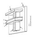
- local interconnectsare conventionally formed over the fins, as illustrated in FIG. 1 .
- one or more fins 101are formed on substrate 103 , with a gate electrode 105 , with a spacer 107 on each side, formed perpendicular to and over the fins.
- a local interconnect 109is also formed over the fins 101 , separated from the gate electrode 105 . Because of the large exposed source/drain contact area (due to the local interconnect) facing the gate in the width direction, the density of field lines from the gate is increased, which in turn increases the parasitic capacitance between the gate and the contact.
- An aspect of the present disclosureis a method of fabricating a buried local interconnect in a finfet structure.
- Another aspect of the present disclosureis a buried local interconnect in a finfet structure.
- some technical effectsmay be achieved in part by a method including: forming a silicon fin on a BOX layer; forming a gate electrode perpendicular to the silicon fin over a portion of the silicon fin; forming a spacer on each of opposite sides of the gate electrode; forming source/drain regions on the silicon fin at opposite sides of the gate electrode; recessing the BOX layer, undercutting the silicon fin and source/drain regions, at opposite sides of the gate electrode; and forming a local interconnect on a recessed portion of the BOX layer.
- aspects of the present disclosureinclude forming a second spacer on each first spacer; and forming a silicide on the source/drain regions.
- Other aspectsinclude depositing tungsten on each side of the gate electrode up to a height of the silicon fin.
- Another aspectincludes forming a via (V0) on the tungsten.
- Further aspectsinclude forming the source/drain regions by epitaxially growing doped silicon germanium (SiGe) around the silicon fin.
- Additional aspectsinclude forming at least one second silicon fin; and merging the fins by the epitaxially growing SiGe around the silicon fins.
- Other aspectsinclude: forming at least one second silicon fin; and forming un-merged fins by the epitaxially growing SiGe around the silicon fins.
- a further aspectincludes recessing the BOX layer by a dry etch and a wet etch. Additional aspects include the dry etch including dry etching with tetrafluoromethane (CF 4 ) plus oxygen (O 2 ), and the wet etch including wet etching with hydrogen fluoride (HF) or buffered HF. An additional aspect includes recessing the BOX layer 20 to 30 nanometers (nm).
- Another aspect of the present disclosureis a device including: a silicon fin on a BOX layer; a gate electrode perpendicular to the silicon fin over a portion of the silicon fin; a spacer on each of opposite sides of the gate electrode; source/drain regions on the silicon fin at opposite sides of the gate electrode, wherein the BOX layer is recessed, undercutting the silicon fin and source/drain regions, at opposite sides of the gate electrode; and a local interconnect on a recessed portion of the BOX layer.
- aspectsinclude: a second spacer on each first spacer; and a silicide on the source/drain regions.
- Other aspectsinclude tungsten on each side of the gate electrode up to a height of the silicon fin. Further aspects include a via (V0) on the tungsten.
- Another aspectincludes the source/drain regions including doped silicon germanium (SiGe) epitaxially grown on exposed surfaces of the silicon fin. Additional aspects include: at least one second silicon fin, wherein the epitaxially grown SiGe forms merged fins. Other aspects include: at least one second silicon fin, wherein the epitaxially grown SiGe forms un-merged fins.
- Another aspectincludes the BOX layer being recessed 20 to 30 nanometers (nm).
- Another aspect of the present disclosureis a method including: forming one or more silicon fins on a BOX layer; forming a gate electrode perpendicular to the one or more silicon fins over a portion of each of the one or more silicon fins; forming a spacer on each of opposite sides of the gate electrode; forming source/drain regions on each of the one or more silicon fins at opposite sides of the gate electrode by epitaxially growing doped silicon germanium (SiGe) around each of the one or more silicon fins; recessing the BOX layer 20 to 30 nanometers (nm) by a dry etch and a wet etch, undercutting each of the one or more silicon fins and source/drain regions, at opposite sides of the gate electrode; forming a second spacer on each first spacer; forming a silicide on the source/drain regions; forming a local interconnect on a recessed portion of the BOX layer; depositing tungsten on each side of the gate electrode up to a height of the one
- FIG. 1schematically illustrates a conventional finfet with a raised local interconnect
- FIGS. 2A and 2B through 6 A and 6 Bschematically illustrate a process of forming finfets with buried local interconnects, in accordance with an exemplary embodiment.
- FIGS. 2A through 6Aillustrate unmerged fins
- FIGS. 2B through 6Billustrate merged fins.
- the present disclosureaddresses and solves the current problem of increased parasitic capacitance from the gate to source/drain contacts attendant upon employing raised local interconnects in finfet devices.
- local interconnectsare buried under the fins by recessing an epi-merged source/drain area to create a cavity for filling with tungsten (W).
- Wtungsten
- Methodology in accordance with embodiments of the present disclosureincludes forming a silicon fin on a BOX layer, forming a gate electrode perpendicular to the silicon fin over a portion of the silicon fin, with a spacer on each of opposite sides of the gate electrode, and forming source/drain regions on the silicon fin at opposite sides of the gate electrode. Then the BOX layer is recessed, undercutting the silicon fin and source/drain regions, at opposite sides of the gate electrode, and a local interconnect is formed on a recessed portion of the BOX layer.
- FIGS. 2A and 2B through 6 A and 6 Ba process of forming finfets with buried local interconnects is illustrated, in accordance with an exemplary embodiment.
- the processbegins the same as a standard finfet flow.
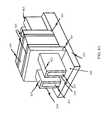
- one or more silicon fins 201are formed on a BOX layer 203 of a silicon-on-insulator (SOI) substrate. Two fins are shown, but a single fin or more than two fins may be employed.
- the gate electrodeis perpendicular to the fins and is insulated from the fins by the gate dielectric.
- Offset spacers 207for example of silicon nitride (SiN) or silicon dioxide (SiO 2 ), are formed on each side of the gate electrode.
- the siliconis doped, and then cladded fins are formed.
- silicon germanium (SiGe) 209is epitaxially grown, wrapping around the fins, for source/drain formation. Alternatively, the epitaxial growth may form merged fins, as shown in FIG. 2B . As illustrated, SiGe 211 is grown over and connecting fins 201 .
- BOX layer 203Prior to a silicon/SiGe extension drive-in step, BOX layer 203 is recessed, completely undercutting the bottoms of fins 201 , as illustrated at 301 in FIGS. 3A and 3B .
- BOX layer 203may be recessed, for example, by a dry etch, such as tetrafluoromethane (CF 4 ) plus oxygen (O 2 ), and a wet etch, such as hydrogen fluoride (HF) or buffered HF, to completely undercut the fin bottom.
- CF 4tetrafluoromethane
- O 2oxygen
- HFhydrogen fluoride
- the recessis formed to a depth of 20 to 30 nanometers.
- the recessis shown only on one side of gate 205 in each of FIGS. 3A and 3B (for illustrative convenience), the recess should be on both sides for both the source and the drain.
- final spacers 401are formed on opposite sides of gate electrode 205 .
- Source/drain SiGe 209 or 211is then ion implanted, and a silicide 403 is formed on exposed SiGe surfaces by conventional processes.
- the gate electrode 205 and gate dielectricmay then be replaced with a high-k dielectric (a dielectric having a dielectric constant greater than 3.9) and a metal gate electrode 405 .
- the metal gatemay be formed by a preclean followed by formation of a titanium (Ti)/titanium nitride (TiN) liner and W main layer.
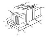
- a buried local interconnect 501is formed in recess 301 .
- Tungsten (W) 503is then filled to the height of the fins to reduce the series resistance. Since the local interconnect is buried underneath the fin, gate-to-contact capacitance is virtually eliminated (with the exception of a slight fringing field at the bottom of the fin).
- the final structuremay include V0 vias 601 from the tungsten fill 503 to the first metallization layer (M1) (not shown for illustrative convenience.
- V0's 601may be filled with aluminum.
- the embodiments of the present disclosurecan achieve several technical effects, such as a buried local interconnect, which in turn eliminates gate-to-contact capacitance.
- the present disclosureenjoys utility in various industrial applications as, for example, microprocessors, smart phones, mobile phones, cellular handsets, set-top boxes, DVD recorders and players, automotive navigation, printers and peripherals, networking and telecom equipment, gaming systems, and digital cameras.
- the present disclosuretherefore enjoys industrial applicability in any of various types of highly integrated semiconductor devices.
Landscapes
- Engineering & Computer Science (AREA)
- Physics & Mathematics (AREA)
- Condensed Matter Physics & Semiconductors (AREA)
- General Physics & Mathematics (AREA)
- Manufacturing & Machinery (AREA)
- Computer Hardware Design (AREA)
- Microelectronics & Electronic Packaging (AREA)
- Power Engineering (AREA)
- Chemical & Material Sciences (AREA)
- Chemical Kinetics & Catalysis (AREA)
- General Chemical & Material Sciences (AREA)
- Insulated Gate Type Field-Effect Transistor (AREA)
Abstract
Description
- The present disclosure relates to local interconnects in semiconductor devices, and more particularly to local interconnects in finfet structures.
- The integration of hundreds of millions of circuit elements, such as transistors, on a single integrated circuit necessitates further dramatic scaling down or micro-miniaturization of the physical dimensions of circuit elements, including interconnection structures. Micro-miniaturization has engendered a dramatic increase in transistor engineering complexity, such as the inclusion of lightly doped drain structures, multiple implants for source/drain regions, silicidation of gates and source/drains, and multiple sidewall spacers, for example. Conductors are routed over dielectric layers to connect to source/drain junctions and gates. The entire process of routing and making connections is generally termed “metalization”.
- As the complexity of metallization has increased, multiple layers of interconnect structures as well as short distance interconnects, or local interconnects, at levels at or below the customary metallization layers have been employed. Local interconnects are a special form of interconnects for very short distances, such as between the gate and drain of an individual semiconductor device.
- In finfet devices, local interconnects are conventionally formed over the fins, as illustrated in
FIG. 1 . As shown, one or more fins101 (two shown) are formed onsubstrate 103, with agate electrode 105, with aspacer 107 on each side, formed perpendicular to and over the fins. Alocal interconnect 109 is also formed over thefins 101, separated from thegate electrode 105. Because of the large exposed source/drain contact area (due to the local interconnect) facing the gate in the width direction, the density of field lines from the gate is increased, which in turn increases the parasitic capacitance between the gate and the contact. - A need therefore exists for methodology enabling formation of local interconnects with a reduced parasitic capacitance between the gate and source/drain contacts and the resulting device.
- An aspect of the present disclosure is a method of fabricating a buried local interconnect in a finfet structure.
- Another aspect of the present disclosure is a buried local interconnect in a finfet structure.
- Additional aspects and other features of the present disclosure will be set forth in the description which follows and in part will be apparent to those having ordinary skill in the art upon examination of the following or may be learned from the practice of the present disclosure. The advantages of the present disclosure may be realized and obtained as particularly pointed out in the appended claims.
- According to the present disclosure, some technical effects may be achieved in part by a method including: forming a silicon fin on a BOX layer; forming a gate electrode perpendicular to the silicon fin over a portion of the silicon fin; forming a spacer on each of opposite sides of the gate electrode; forming source/drain regions on the silicon fin at opposite sides of the gate electrode; recessing the BOX layer, undercutting the silicon fin and source/drain regions, at opposite sides of the gate electrode; and forming a local interconnect on a recessed portion of the BOX layer.
- Aspects of the present disclosure include forming a second spacer on each first spacer; and forming a silicide on the source/drain regions. Other aspects include depositing tungsten on each side of the gate electrode up to a height of the silicon fin. Another aspect includes forming a via (V0) on the tungsten. Further aspects include forming the source/drain regions by epitaxially growing doped silicon germanium (SiGe) around the silicon fin. Additional aspects include forming at least one second silicon fin; and merging the fins by the epitaxially growing SiGe around the silicon fins. Other aspects include: forming at least one second silicon fin; and forming un-merged fins by the epitaxially growing SiGe around the silicon fins. A further aspect includes recessing the BOX layer by a dry etch and a wet etch. Additional aspects include the dry etch including dry etching with tetrafluoromethane (CF4) plus oxygen (O2), and the wet etch including wet etching with hydrogen fluoride (HF) or buffered HF. An additional aspect includes recessing the BOX layer 20 to 30 nanometers (nm).
- Another aspect of the present disclosure is a device including: a silicon fin on a BOX layer; a gate electrode perpendicular to the silicon fin over a portion of the silicon fin; a spacer on each of opposite sides of the gate electrode; source/drain regions on the silicon fin at opposite sides of the gate electrode, wherein the BOX layer is recessed, undercutting the silicon fin and source/drain regions, at opposite sides of the gate electrode; and a local interconnect on a recessed portion of the BOX layer.
- Aspects include: a second spacer on each first spacer; and a silicide on the source/drain regions. Other aspects include tungsten on each side of the gate electrode up to a height of the silicon fin. Further aspects include a via (V0) on the tungsten. Another aspect includes the source/drain regions including doped silicon germanium (SiGe) epitaxially grown on exposed surfaces of the silicon fin. Additional aspects include: at least one second silicon fin, wherein the epitaxially grown SiGe forms merged fins. Other aspects include: at least one second silicon fin, wherein the epitaxially grown SiGe forms un-merged fins. Another aspect includes the BOX layer being recessed 20 to 30 nanometers (nm).
- Another aspect of the present disclosure is a method including: forming one or more silicon fins on a BOX layer; forming a gate electrode perpendicular to the one or more silicon fins over a portion of each of the one or more silicon fins; forming a spacer on each of opposite sides of the gate electrode; forming source/drain regions on each of the one or more silicon fins at opposite sides of the gate electrode by epitaxially growing doped silicon germanium (SiGe) around each of the one or more silicon fins; recessing the BOX layer 20 to 30 nanometers (nm) by a dry etch and a wet etch, undercutting each of the one or more silicon fins and source/drain regions, at opposite sides of the gate electrode; forming a second spacer on each first spacer; forming a silicide on the source/drain regions; forming a local interconnect on a recessed portion of the BOX layer; depositing tungsten on each side of the gate electrode up to a height of the one or more silicon fins; and forming a via (V0) on the tungsten. A further aspect includes the epitaxially grown SiGe forming cladded fins.
- Additional aspects and technical effects of the present disclosure will become readily apparent to those skilled in the art from the following detailed description wherein embodiments of the present disclosure are described simply by way of illustration of the best mode contemplated to carry out the present disclosure. As will be realized, the present disclosure is capable of other and different embodiments, and its several details are capable of modifications in various obvious respects, all without departing from the present disclosure. Accordingly, the drawings and description are to be regarded as illustrative in nature, and not as restrictive.
- The present disclosure is illustrated by way of example, and not by way of limitation, in the figures of the accompanying drawing and in which like reference numerals refer to similar elements and in which:
FIG. 1 schematically illustrates a conventional finfet with a raised local interconnect; andFIGS. 2A and 2B through6A and6B schematically illustrate a process of forming finfets with buried local interconnects, in accordance with an exemplary embodiment.FIGS. 2A through 6A illustrate unmerged fins, andFIGS. 2B through 6B illustrate merged fins.- In the following description, for the purposes of explanation, numerous specific details are set forth in order to provide a thorough understanding of exemplary embodiments. It should be apparent, however, that exemplary embodiments may be practiced without these specific details or with an equivalent arrangement. In other instances, well-known structures and devices are shown in block diagram form in order to avoid unnecessarily obscuring exemplary embodiments. In addition, unless otherwise indicated, all numbers expressing quantities, ratios, and numerical properties of ingredients, reaction conditions, and so forth used in the specification and claims are to be understood as being modified in all instances by the term “about.”
- The present disclosure addresses and solves the current problem of increased parasitic capacitance from the gate to source/drain contacts attendant upon employing raised local interconnects in finfet devices. In accordance with embodiments of the present disclosure, local interconnects are buried under the fins by recessing an epi-merged source/drain area to create a cavity for filling with tungsten (W). The buried local interconnects reduce the exposed contact area facing the gate, which in turn reduces the density of field lines from the gate.
- Methodology in accordance with embodiments of the present disclosure includes forming a silicon fin on a BOX layer, forming a gate electrode perpendicular to the silicon fin over a portion of the silicon fin, with a spacer on each of opposite sides of the gate electrode, and forming source/drain regions on the silicon fin at opposite sides of the gate electrode. Then the BOX layer is recessed, undercutting the silicon fin and source/drain regions, at opposite sides of the gate electrode, and a local interconnect is formed on a recessed portion of the BOX layer.
- Still other aspects, features, and technical effects will be readily apparent to those skilled in this art from the following detailed description, wherein preferred embodiments are shown and described, simply by way of illustration of the best mode contemplated. The disclosure is capable of other and different embodiments, and its several details are capable of modifications in various obvious respects. Accordingly, the drawings and description are to be regarded as illustrative in nature, and not as restrictive.
- Adverting to
FIGS. 2A and 2B through6A and6B, a process of forming finfets with buried local interconnects is illustrated, in accordance with an exemplary embodiment. As illustrated inFIG. 2A , the process begins the same as a standard finfet flow. Specifically, one ormore silicon fins 201 are formed on aBOX layer 203 of a silicon-on-insulator (SOI) substrate. Two fins are shown, but a single fin or more than two fins may be employed. A gate dielectric, such as silicon oxide (not shown for illustrative convenience), andgate electrode 205, such as a polysilicon dummy gate, are formed over thefins 201. The gate electrode is perpendicular to the fins and is insulated from the fins by the gate dielectric. Offsetspacers 207, for example of silicon nitride (SiN) or silicon dioxide (SiO2), are formed on each side of the gate electrode. The silicon is doped, and then cladded fins are formed. More specifically, silicon germanium (SiGe)209 is epitaxially grown, wrapping around the fins, for source/drain formation. Alternatively, the epitaxial growth may form merged fins, as shown inFIG. 2B . As illustrated,SiGe 211 is grown over and connectingfins 201. - Prior to a silicon/SiGe extension drive-in step,
BOX layer 203 is recessed, completely undercutting the bottoms offins 201, as illustrated at301 inFIGS. 3A and 3B .BOX layer 203 may be recessed, for example, by a dry etch, such as tetrafluoromethane (CF4) plus oxygen (O2), and a wet etch, such as hydrogen fluoride (HF) or buffered HF, to completely undercut the fin bottom. The recess is formed to a depth of 20 to 30 nanometers. Although the recess is shown only on one side ofgate 205 in each ofFIGS. 3A and 3B (for illustrative convenience), the recess should be on both sides for both the source and the drain. - Adverting to
FIGS. 4A and 4B ,final spacers 401 are formed on opposite sides ofgate electrode 205. Source/drain SiGe silicide 403 is formed on exposed SiGe surfaces by conventional processes. Thegate electrode 205 and gate dielectric may then be replaced with a high-k dielectric (a dielectric having a dielectric constant greater than 3.9) and ametal gate electrode 405. The metal gate may be formed by a preclean followed by formation of a titanium (Ti)/titanium nitride (TiN) liner and W main layer. - As illustrated in
FIGS. 5A and 5B , a buriedlocal interconnect 501 is formed inrecess 301. Tungsten (W)503 is then filled to the height of the fins to reduce the series resistance. Since the local interconnect is buried underneath the fin, gate-to-contact capacitance is virtually eliminated (with the exception of a slight fringing field at the bottom of the fin). - As illustrated in
FIGS. 6A and 6B , the final structure may include V0 vias601 from the tungsten fill503 to the first metallization layer (M1) (not shown for illustrative convenience. V0's601 may be filled with aluminum. - The embodiments of the present disclosure can achieve several technical effects, such as a buried local interconnect, which in turn eliminates gate-to-contact capacitance. The present disclosure enjoys utility in various industrial applications as, for example, microprocessors, smart phones, mobile phones, cellular handsets, set-top boxes, DVD recorders and players, automotive navigation, printers and peripherals, networking and telecom equipment, gaming systems, and digital cameras. The present disclosure therefore enjoys industrial applicability in any of various types of highly integrated semiconductor devices.
- In the preceding description, the present disclosure is described with reference to specifically exemplary embodiments thereof. It will, however, be evident that various modifications and changes may be made thereto without departing from the broader spirit and scope of the present disclosure, as set forth in the claims. The specification and drawings are, accordingly, to be regarded as illustrative and not as restrictive. It is understood that the present disclosure is capable of using various other combinations and embodiments and is capable of any changes or modifications within the scope of the inventive concept as expressed herein.
Claims (20)
Priority Applications (1)
| Application Number | Priority Date | Filing Date | Title |
|---|---|---|---|
| US14/135,716US9324842B2 (en) | 2013-12-20 | 2013-12-20 | Buried local interconnect in finfet structure and method of fabricating same |
Applications Claiming Priority (1)
| Application Number | Priority Date | Filing Date | Title |
|---|---|---|---|
| US14/135,716US9324842B2 (en) | 2013-12-20 | 2013-12-20 | Buried local interconnect in finfet structure and method of fabricating same |
Publications (2)
| Publication Number | Publication Date |
|---|---|
| US20150179766A1true US20150179766A1 (en) | 2015-06-25 |
| US9324842B2 US9324842B2 (en) | 2016-04-26 |
Family
ID=53400977
Family Applications (1)
| Application Number | Title | Priority Date | Filing Date |
|---|---|---|---|
| US14/135,716Expired - Fee RelatedUS9324842B2 (en) | 2013-12-20 | 2013-12-20 | Buried local interconnect in finfet structure and method of fabricating same |
Country Status (1)
| Country | Link |
|---|---|
| US (1) | US9324842B2 (en) |
Cited By (4)
| Publication number | Priority date | Publication date | Assignee | Title |
|---|---|---|---|---|
| US10170620B2 (en) | 2016-05-18 | 2019-01-01 | International Business Machines Corporation | Substantially defect free relaxed heterogeneous semiconductor fins on bulk substrates |
| EP3629368A3 (en)* | 2018-06-07 | 2020-04-08 | INTEL Corporation | Device layer interconnects |
| WO2023078083A1 (en)* | 2021-11-03 | 2023-05-11 | International Business Machines Corporation | Integrated short channel omega gate finfet and long channel finfet |
| TWI828304B (en)* | 2021-10-20 | 2024-01-01 | 台灣積體電路製造股份有限公司 | Semiconductor device structure and method for forming the same |
Families Citing this family (3)
| Publication number | Priority date | Publication date | Assignee | Title |
|---|---|---|---|---|
| US9263555B2 (en)* | 2014-07-03 | 2016-02-16 | Globalfoundries Inc. | Methods of forming a channel region for a semiconductor device by performing a triple cladding process |
| US10756096B2 (en) | 2018-10-05 | 2020-08-25 | Globalfoundries Inc. | Integrated circuit structure with complementary field effect transistor and buried metal interconnect and method |
| EP3671825A1 (en) | 2018-12-20 | 2020-06-24 | IMEC vzw | Method for connecting a buried interconnect rail and a semiconductor fin in an integrated circuit chip |
Citations (6)
| Publication number | Priority date | Publication date | Assignee | Title |
|---|---|---|---|---|
| US20040262692A1 (en)* | 2003-06-27 | 2004-12-30 | Hareland Scott A. | Nonplanar device with stress incorporation layer and method of fabrication |
| US20060138553A1 (en)* | 2004-09-30 | 2006-06-29 | Brask Justin K | Nonplanar transistors with metal gate electrodes |
| US20070210355A1 (en)* | 2006-03-06 | 2007-09-13 | Kabushiki Kaisha Toshiba | Semiconductor device |
| US20110147840A1 (en)* | 2009-12-23 | 2011-06-23 | Cea Stephen M | Wrap-around contacts for finfet and tri-gate devices |
| US20110193141A1 (en)* | 2010-02-11 | 2011-08-11 | Taiwan Semiconductor Manufacturing Company, Ltd. | Method of fabricating a finfet device |
| US8900951B1 (en)* | 2013-09-24 | 2014-12-02 | International Business Machines Corporation | Gate-all-around nanowire MOSFET and method of formation |
Family Cites Families (1)
| Publication number | Priority date | Publication date | Assignee | Title |
|---|---|---|---|---|
| US6054385A (en) | 1997-01-31 | 2000-04-25 | Advanced Micro Devices, Inc. | Elevated local interconnect and contact structure |
- 2013
- 2013-12-20USUS14/135,716patent/US9324842B2/ennot_activeExpired - Fee Related
Patent Citations (6)
| Publication number | Priority date | Publication date | Assignee | Title |
|---|---|---|---|---|
| US20040262692A1 (en)* | 2003-06-27 | 2004-12-30 | Hareland Scott A. | Nonplanar device with stress incorporation layer and method of fabrication |
| US20060138553A1 (en)* | 2004-09-30 | 2006-06-29 | Brask Justin K | Nonplanar transistors with metal gate electrodes |
| US20070210355A1 (en)* | 2006-03-06 | 2007-09-13 | Kabushiki Kaisha Toshiba | Semiconductor device |
| US20110147840A1 (en)* | 2009-12-23 | 2011-06-23 | Cea Stephen M | Wrap-around contacts for finfet and tri-gate devices |
| US20110193141A1 (en)* | 2010-02-11 | 2011-08-11 | Taiwan Semiconductor Manufacturing Company, Ltd. | Method of fabricating a finfet device |
| US8900951B1 (en)* | 2013-09-24 | 2014-12-02 | International Business Machines Corporation | Gate-all-around nanowire MOSFET and method of formation |
Cited By (11)
| Publication number | Priority date | Publication date | Assignee | Title |
|---|---|---|---|---|
| US10170620B2 (en) | 2016-05-18 | 2019-01-01 | International Business Machines Corporation | Substantially defect free relaxed heterogeneous semiconductor fins on bulk substrates |
| US10734518B2 (en) | 2016-05-18 | 2020-08-04 | International Business Machines Corporation | Substantially defect free relaxed heterogeneous semiconductor fins on bulk substrates |
| US10833192B2 (en) | 2016-05-18 | 2020-11-10 | International Business Machines Corporation | Substantially defect free relaxed heterogeneous semiconductor fins on bulk substrates |
| EP3629368A3 (en)* | 2018-06-07 | 2020-04-08 | INTEL Corporation | Device layer interconnects |
| US11410928B2 (en) | 2018-06-07 | 2022-08-09 | Intel Corporation | Device layer interconnects |
| TWI818016B (en)* | 2018-06-07 | 2023-10-11 | 美商英特爾股份有限公司 | Device layer interconnects |
| US11881452B2 (en) | 2018-06-07 | 2024-01-23 | Intel Corporation | Device layer interconnects |
| TWI828304B (en)* | 2021-10-20 | 2024-01-01 | 台灣積體電路製造股份有限公司 | Semiconductor device structure and method for forming the same |
| US12419097B2 (en) | 2021-10-20 | 2025-09-16 | Taiwan Semiconductor Manufacturing Co., Ltd | Semiconductor device structure and method for forming the same |
| WO2023078083A1 (en)* | 2021-11-03 | 2023-05-11 | International Business Machines Corporation | Integrated short channel omega gate finfet and long channel finfet |
| US12100766B2 (en) | 2021-11-03 | 2024-09-24 | International Business Machines Corporation | Integrated short channel omega gate FinFET and long channel FinFET |
Also Published As
| Publication number | Publication date |
|---|---|
| US9324842B2 (en) | 2016-04-26 |
Similar Documents
| Publication | Publication Date | Title |
|---|---|---|
| US9324842B2 (en) | Buried local interconnect in finfet structure and method of fabricating same | |
| US9911851B2 (en) | Integrated circuit devices having air-gap spacers above gate electrodes | |
| KR102235578B1 (en) | Semiconductor device and the method for fabricating thereof | |
| US8697539B2 (en) | Method of making lower parasitic capacitance FinFET | |
| TWI573222B (en) | Semiconductor device and method of manufacturing same | |
| US9431478B2 (en) | Semiconductor device and method of fabricating the same | |
| US7948027B1 (en) | Embedded bit line structure, field effect transistor structure with the same and method of fabricating the same | |
| US10714473B2 (en) | Semiconductor device | |
| US9318575B2 (en) | Semiconductor device and method for fabricating the same | |
| US9679965B1 (en) | Semiconductor device having a gate all around structure and a method for fabricating the same | |
| US10490637B2 (en) | Semiconductor devices including an active fin and a drift region | |
| US20170018610A1 (en) | Semiconductor device having a fin | |
| US10236363B2 (en) | Vertical field-effect transistors with controlled dimensions | |
| US9871042B2 (en) | Semiconductor device having fin-type patterns | |
| US20120193713A1 (en) | FinFET device having reduce capacitance, access resistance, and contact resistance | |
| US20170110456A1 (en) | Semiconductor devices including insulating materials in fins | |
| US9349858B2 (en) | Semiconductor device and method of fabricating the same | |
| KR20160035650A (en) | Semiconductor device and method of manufacturing the same | |
| US20150132908A1 (en) | Method for fabricating semiconductor device | |
| US20160276342A1 (en) | Semiconductor devices including shallow trench isolation (sti) liners | |
| US20180337033A1 (en) | Novel approach to improve sdb device performance | |
| US8946802B2 (en) | Method of eDRAM DT strap formation in FinFET device structure | |
| US9324831B2 (en) | Forming transistors without spacers and resulting devices | |
| US9362311B1 (en) | Method of fabricating semiconductor device | |
| US9385120B2 (en) | Semiconductor device and method of fabricating the same |
Legal Events
| Date | Code | Title | Description |
|---|---|---|---|
| AS | Assignment | Owner name:GLOBALFOUNDRIES INC., CAYMAN ISLANDS Free format text:ASSIGNMENT OF ASSIGNORS INTEREST;ASSIGNORS:ZANG, HUI;YEH, CHUN-CHEN;YAMASHITA, TENKO;AND OTHERS;SIGNING DATES FROM 20131106 TO 20131107;REEL/FRAME:031826/0217 | |
| AS | Assignment | Owner name:INTERNATIONAL BUSINESS MACHINES CORPORATION, NEW Y Free format text:ASSIGNMENT OF ASSIGNORS INTEREST;ASSIGNORS:ZANG, HUI;YEH, CHUN-CHEN;YAMASHITA, TENKO;AND OTHERS;SIGNING DATES FROM 20131107 TO 20150326;REEL/FRAME:035332/0187 Owner name:GLOBALFOUNDRIES INC., CAYMAN ISLANDS Free format text:ASSIGNMENT OF ASSIGNORS INTEREST;ASSIGNORS:ZANG, HUI;YEH, CHUN-CHEN;YAMASHITA, TENKO;AND OTHERS;SIGNING DATES FROM 20131107 TO 20150326;REEL/FRAME:035332/0187 | |
| FEPP | Fee payment procedure | Free format text:PAYOR NUMBER ASSIGNED (ORIGINAL EVENT CODE: ASPN); ENTITY STATUS OF PATENT OWNER: LARGE ENTITY | |
| STCF | Information on status: patent grant | Free format text:PATENTED CASE | |
| AS | Assignment | Owner name:ALSEPHINA INNOVATIONS INC., CANADA Free format text:ASSIGNMENT OF ASSIGNORS INTEREST;ASSIGNOR:GLOBALFOUNDRIES INC.;REEL/FRAME:049669/0749 Effective date:20181126 | |
| FEPP | Fee payment procedure | Free format text:MAINTENANCE FEE REMINDER MAILED (ORIGINAL EVENT CODE: REM.); ENTITY STATUS OF PATENT OWNER: LARGE ENTITY | |
| LAPS | Lapse for failure to pay maintenance fees | Free format text:PATENT EXPIRED FOR FAILURE TO PAY MAINTENANCE FEES (ORIGINAL EVENT CODE: EXP.); ENTITY STATUS OF PATENT OWNER: LARGE ENTITY | |
| STCH | Information on status: patent discontinuation | Free format text:PATENT EXPIRED DUE TO NONPAYMENT OF MAINTENANCE FEES UNDER 37 CFR 1.362 | |
| FP | Lapsed due to failure to pay maintenance fee | Effective date:20200426 | |
| AS | Assignment | Owner name:GLOBALFOUNDRIES INC., CAYMAN ISLANDS Free format text:RELEASE BY SECURED PARTY;ASSIGNOR:WILMINGTON TRUST, NATIONAL ASSOCIATION;REEL/FRAME:054636/0001 Effective date:20201117 |