US20150177619A1 - Plasmonic lithography using phase mask - Google Patents
Plasmonic lithography using phase maskDownload PDFInfo
- Publication number
- US20150177619A1 US20150177619A1US14/229,762US201414229762AUS2015177619A1US 20150177619 A1US20150177619 A1US 20150177619A1US 201414229762 AUS201414229762 AUS 201414229762AUS 2015177619 A1US2015177619 A1US 2015177619A1
- Authority
- US
- United States
- Prior art keywords
- mask
- photoresist
- features
- metal
- pattern
- Prior art date
- Legal status (The legal status is an assumption and is not a legal conclusion. Google has not performed a legal analysis and makes no representation as to the accuracy of the status listed.)
- Granted
Links
- 238000001459lithographyMethods0.000titledescription8
- 229910052751metalInorganic materials0.000claimsabstractdescription45
- 239000002184metalSubstances0.000claimsabstractdescription45
- 229920002120photoresistant polymerPolymers0.000claimsabstractdescription44
- 238000000034methodMethods0.000claimsabstractdescription29
- 239000000758substrateSubstances0.000claimsabstractdescription23
- 230000005855radiationEffects0.000claimsabstractdescription22
- 239000000463materialSubstances0.000claimsabstractdescription21
- 235000013870dimethyl polysiloxaneNutrition0.000claimsdescription9
- 239000004205dimethyl polysiloxaneSubstances0.000claimsdescription9
- 229920000435poly(dimethylsiloxane)Polymers0.000claimsdescription9
- 229920001971elastomerPolymers0.000claimsdescription7
- 239000000806elastomerSubstances0.000claimsdescription7
- 238000005530etchingMethods0.000claimsdescription3
- 239000011248coating agentSubstances0.000claimsdescription2
- 238000000576coating methodMethods0.000claimsdescription2
- 230000002301combined effectEffects0.000claimsdescription2
- 229910052782aluminiumInorganic materials0.000claims1
- XAGFODPZIPBFFR-UHFFFAOYSA-NaluminiumChemical compound[Al]XAGFODPZIPBFFR-UHFFFAOYSA-N0.000claims1
- 238000005329nanolithographyMethods0.000abstractdescription10
- 230000005284excitationEffects0.000abstractdescription3
- 239000010410layerSubstances0.000description29
- 239000012071phaseSubstances0.000description10
- 238000005096rolling processMethods0.000description7
- 238000009826distributionMethods0.000description6
- 230000005684electric fieldEffects0.000description6
- 238000001527near-field phase shift lithographyMethods0.000description6
- 238000005516engineering processMethods0.000description4
- 230000000737periodic effectEffects0.000description4
- 101100269850Caenorhabditis elegans mask-1 geneProteins0.000description3
- 238000010586diagramMethods0.000description3
- 230000010363phase shiftEffects0.000description3
- 238000000231atomic layer depositionMethods0.000description2
- 238000005229chemical vapour depositionMethods0.000description2
- 238000000206photolithographyMethods0.000description2
- 229920000642polymerPolymers0.000description2
- 239000010453quartzSubstances0.000description2
- 239000013545self-assembled monolayerSubstances0.000description2
- VYPSYNLAJGMNEJ-UHFFFAOYSA-Nsilicon dioxideInorganic materialsO=[Si]=OVYPSYNLAJGMNEJ-UHFFFAOYSA-N0.000description2
- 239000005328architectural glassSubstances0.000description1
- 238000000276deep-ultraviolet lithographyMethods0.000description1
- 230000001419dependent effectEffects0.000description1
- 238000000151depositionMethods0.000description1
- 239000011521glassSubstances0.000description1
- 238000005286illuminationMethods0.000description1
- 239000012212insulatorSubstances0.000description1
- 239000007791liquid phaseSubstances0.000description1
- 238000004519manufacturing processMethods0.000description1
- QSHDDOUJBYECFT-UHFFFAOYSA-NmercuryChemical compound[Hg]QSHDDOUJBYECFT-UHFFFAOYSA-N0.000description1
- 229910052753mercuryInorganic materials0.000description1
- 239000007769metal materialSubstances0.000description1
- 239000002082metal nanoparticleSubstances0.000description1
- 238000012986modificationMethods0.000description1
- 230000004048modificationEffects0.000description1
- 238000001127nanoimprint lithographyMethods0.000description1
- 239000002086nanomaterialSubstances0.000description1
- 239000002105nanoparticleSubstances0.000description1
- 238000000054nanosphere lithographyMethods0.000description1
- 230000001902propagating effectEffects0.000description1
- 239000004065semiconductorSubstances0.000description1
- 230000035945sensitivityEffects0.000description1
- 230000003595spectral effectEffects0.000description1
- 239000012780transparent materialSubstances0.000description1
- 239000012808vapor phaseSubstances0.000description1
Images


Classifications
- G—PHYSICS
- G03—PHOTOGRAPHY; CINEMATOGRAPHY; ANALOGOUS TECHNIQUES USING WAVES OTHER THAN OPTICAL WAVES; ELECTROGRAPHY; HOLOGRAPHY
- G03F—PHOTOMECHANICAL PRODUCTION OF TEXTURED OR PATTERNED SURFACES, e.g. FOR PRINTING, FOR PROCESSING OF SEMICONDUCTOR DEVICES; MATERIALS THEREFOR; ORIGINALS THEREFOR; APPARATUS SPECIALLY ADAPTED THEREFOR
- G03F1/00—Originals for photomechanical production of textured or patterned surfaces, e.g., masks, photo-masks, reticles; Mask blanks or pellicles therefor; Containers specially adapted therefor; Preparation thereof
- G03F1/26—Phase shift masks [PSM]; PSM blanks; Preparation thereof
- G—PHYSICS
- G03—PHOTOGRAPHY; CINEMATOGRAPHY; ANALOGOUS TECHNIQUES USING WAVES OTHER THAN OPTICAL WAVES; ELECTROGRAPHY; HOLOGRAPHY
- G03F—PHOTOMECHANICAL PRODUCTION OF TEXTURED OR PATTERNED SURFACES, e.g. FOR PRINTING, FOR PROCESSING OF SEMICONDUCTOR DEVICES; MATERIALS THEREFOR; ORIGINALS THEREFOR; APPARATUS SPECIALLY ADAPTED THEREFOR
- G03F7/00—Photomechanical, e.g. photolithographic, production of textured or patterned surfaces, e.g. printing surfaces; Materials therefor, e.g. comprising photoresists; Apparatus specially adapted therefor
- G03F7/20—Exposure; Apparatus therefor
- G—PHYSICS
- G03—PHOTOGRAPHY; CINEMATOGRAPHY; ANALOGOUS TECHNIQUES USING WAVES OTHER THAN OPTICAL WAVES; ELECTROGRAPHY; HOLOGRAPHY
- G03F—PHOTOMECHANICAL PRODUCTION OF TEXTURED OR PATTERNED SURFACES, e.g. FOR PRINTING, FOR PROCESSING OF SEMICONDUCTOR DEVICES; MATERIALS THEREFOR; ORIGINALS THEREFOR; APPARATUS SPECIALLY ADAPTED THEREFOR
- G03F1/00—Originals for photomechanical production of textured or patterned surfaces, e.g., masks, photo-masks, reticles; Mask blanks or pellicles therefor; Containers specially adapted therefor; Preparation thereof
- G03F1/50—Mask blanks not covered by G03F1/20 - G03F1/34; Preparation thereof
- G—PHYSICS
- G03—PHOTOGRAPHY; CINEMATOGRAPHY; ANALOGOUS TECHNIQUES USING WAVES OTHER THAN OPTICAL WAVES; ELECTROGRAPHY; HOLOGRAPHY
- G03F—PHOTOMECHANICAL PRODUCTION OF TEXTURED OR PATTERNED SURFACES, e.g. FOR PRINTING, FOR PROCESSING OF SEMICONDUCTOR DEVICES; MATERIALS THEREFOR; ORIGINALS THEREFOR; APPARATUS SPECIALLY ADAPTED THEREFOR
- G03F7/00—Photomechanical, e.g. photolithographic, production of textured or patterned surfaces, e.g. printing surfaces; Materials therefor, e.g. comprising photoresists; Apparatus specially adapted therefor
- G03F7/0035—Multiple processes, e.g. applying a further resist layer on an already in a previously step, processed pattern or textured surface
- G—PHYSICS
- G03—PHOTOGRAPHY; CINEMATOGRAPHY; ANALOGOUS TECHNIQUES USING WAVES OTHER THAN OPTICAL WAVES; ELECTROGRAPHY; HOLOGRAPHY
- G03F—PHOTOMECHANICAL PRODUCTION OF TEXTURED OR PATTERNED SURFACES, e.g. FOR PRINTING, FOR PROCESSING OF SEMICONDUCTOR DEVICES; MATERIALS THEREFOR; ORIGINALS THEREFOR; APPARATUS SPECIALLY ADAPTED THEREFOR
- G03F7/00—Photomechanical, e.g. photolithographic, production of textured or patterned surfaces, e.g. printing surfaces; Materials therefor, e.g. comprising photoresists; Apparatus specially adapted therefor
- G03F7/70—Microphotolithographic exposure; Apparatus therefor
- G03F7/70216—Mask projection systems
- G03F7/70283—Mask effects on the imaging process
Definitions
- Embodiments of the inventionrelate to photolithography and more particularly to plasmonic lithography which employs metallic nanostructures to manipulate the flow of light and exposure of a photoresist.
- Nanostructuringis necessary for many present applications and industries and for new technologies and future advanced products, such as wire grid polarizers for flat panel displays or architectural glass.
- Nanostructured substratesmay be fabricated using techniques such as e-beam direct writing, deep UV lithography, nanosphere lithography, nanoimprint lithography, near-field phase shift lithography, and plasmonic lithography, for example.
- a method of nanopatterning large areas of rigid and flexible substrate materials based on near-field optical lithographyis described in International Patent Application Publication WO02009094009 and U.S. Patent Application Publication US20090297989, both of which are incorporated herein by reference.
- a rotatable maskis used to controllably expose a radiation-sensitive material.
- the rotatable maskcomprises a cylinder or cone.
- the nanopatterning techniquemakes use of near-field photolithography, where the mask used to pattern the substrate is in contact with the substrate.
- Near-field photolithographymay make use of an elastomeric phase-shifting mask, or may employ surface plasmon technology, where a rotating cylinder surface comprises metal nano holes or nanoparticles.
- such a maskis a near-field phase-shift mask.
- Near-field phase shift lithographyinvolves exposure of a photoresist layer to ultraviolet (UV) light that passes through an elastomeric phase mask while the mask is in conformal contact with a photoresist. Bringing an elastomeric phase mask into contact with a thin layer of photoresist causes the photoresist to “wet” the surface of the contact surface of the mask. Passing UV light through the mask while it is in contact with the photoresist exposes the photoresist to the distribution of light intensity that develops at the surface of the mask.
- a phase maskis formed with a depth of relief that is designed to modulate the phase of the transmitted light by it radians.
- a local null in the intensityappears at step edges in the relief pattern formed on the mask.
- a positive photoresistis used, exposure through such a mask, followed by development, yields a line of photoresist with a width equal to the characteristic width of the null in intensity.
- the width of the null in intensityis approximately 100 nm.
- a PDMS maskcan be used to form a conformal, atomic scale contact with a layer of photoresist. This contact is established spontaneously upon contact, without applied pressure.
- PDMSis transparent to UV light with wavelengths greater than 300 nm. Passing light from a mercury lamp (where the main spectral lines are at 355-365 nm) through the PDMS while it is in conformal contact with a layer of photoresist exposes the photoresist to the intensity distribution that forms at the mask.
- the maskmay include surface plasmon technology in which a patterned metal layer or film is laminated or deposited onto the outer surface of a mask.
- the metal layer or filmhas a specific series of through nanoholes.
- a layer of metal nanoparticlesis deposited on the transparent mask's outer surface, to achieve the surface plasmons by enhanced nanopatterning.
- Embodiments of the present inventionaddress the problem of plasmonic printing using an elastomeric phase mask.
- an underlying transparent substrateis coated with a blanket layer of metal.
- the metal layeris then coated with a photoresist.
- a non-metallic phase mask having a pattern of features with a characteristic spatial periodis placed against the photoresist.
- the metal layeris then exposed to radiation of a characteristic vacuum wavelength through the transparent substrate.
- the resist and metal layermay be exposed to the radiation through the non-metallic mask provided the resist layer is sufficiently thin and/or transparent.
- the spatial period of the mask features and the vacuum wavelength of the radiationcan be chosen so that the radiation excites surface plasmons at the interface between the metal and the photoresist.
- the surface plasmonshave a characteristic wavelength equal to the period of the surface features.
- the spatial period of variation in the electric field of the surface plasmonsis the same as the characteristic wavelength of the surface plasmons.
- the spatial period of variation of intensity of the surface plasmonsis proportional to the square of the electric field.
- the spatial period of variation of intensity distribution produced by two counter-propagating surface plasmonsis half the wavelength of the surface plasmons and can equal half the spatial period of features in a mask that launches the counter-propagating surface plasmons.
- Embodiments of the present inventionpertain to methods useful in fabrication of near-field optical lithography masks for “Rolling mask” lithography.
- a cylindrical maskis coated with a polymer, which is patterned with desired features in order to obtain a mask for phase-shift lithography or plasmonic lithography.
- the polymere.g., an elastomer
- FIG. 1is a schematic diagram illustrating conventional surface plasmon resonant interference nano lithography.
- FIGS. 2A-2Care a sequence of schematic diagrams illustrating surface plasmon resonant interference nanolithography in accordance with an embodiment of the present invention.
- FIG. 3is a schematic diagram illustrating the use of a “Rolling Mask” lithography system to implement plasmon resonant interference nanolithography in accordance with an embodiment of the present invention.
- FIG. 1illustrates conventional plasmon resonant nanolithography process.
- a metallic mask 1 with a plurality of featuresmay be fabricated on a thin quartz substrate 2 .
- Incident radiation 3 of wavelength ⁇flows through the mask 1 and illuminates a photoresist layer 4 formed on an underlying substrate 5 , which traditionally is an insulator or semiconductor. In traditional photolithography, this would be a typical diffraction limited exposure and features smaller than approximately ⁇ /2 normally could not be realized.
- the resonant excitation of surface electromagnetic waves on the metallic surfaces(known as surface plasmons) provides a way to get around the diffraction limit.
- the basic principle of plasmon resonant interference nanolithographyis based on the idea that with the aid of a periodic or non-periodic corrugation or a prism, illumination light can couple with surface plasmons (SPs) to obtain a new state also often referred to as a surface plasmon polariton (SPP), which has high field intensity at a metal surface and can exhibit a much shorter wavelength compared to that of illuminating radiation.
- SPssurface plasmons
- the periodicity of the SPPcan be smaller than the periodicity ⁇ of the mask 1 that induces excitation of the SPPs.
- the interference of SPPs propagating in opposite directionscan result in a strongly enhanced nanoscale spatial distribution of an electrical field near the metal surface. Because the intensity of the SPP depends on the square of the electrical field the photoresist 4 can be subjected to an intensity distribution pattern with an even smaller periodicity than that of SPP waves.
- the resonant plasmon wavelength ⁇ plasmon for the weak corrugation limit and normal incidence radiationcan be expressed as
- ⁇is a spatial periodicity in the mask pattern
- ⁇is the resonant frequency
- ⁇ mis the frequency-dependent dielectric constant of the metal
- ⁇ dis the dielectric constant of the adjacent dielectric.
- the disadvantage of the technique shown in FIG. 1is that it is difficult to fabricate a metal mask on many types of mask materials used for phase masks. In particular, it is difficult, indeed it is often impossible, to fabricate a metal mask on a substrate made of an elastomer material such as PDMS. Moreover, a metal layer deposited on nano-scale patterned phase mask may change features dimensions and shape, which is undesirable. Also, metal material covering elastomeric mask makes it less “sticky” and may lead to a slippage problem during a dynamic exposure process. To overcome this disadvantage, embodiments of the present invention utilize a phase mask having a mask pattern that is not made of metal. Another technique used in the past, depositing metal layer on top of photoresist material, is not desirable due to possibility of affecting photoresist sensitivity, surface smoothness and slippage problems outlined above.
- FIGS. 2A-2Cillustrate surface plasmon resonant interference nanolithography in accordance with an embodiment of the present invention.
- a transparent mask 6may have a pattern of corrugated features of periodicity ⁇ and width w.
- the mask 6may be made of any suitable transparent material.
- the transparent mask 6is not made of metal or other material that supports surface plasmons.
- the mask 6is made of a material that does not support surface plasmons.
- the mask 6may be made, e.g., of an elastomer material, such as PDMS.
- a mask made of an elastomer materialis sometimes referred to as a “softmask” or “soft mask”.
- the featuresmay be a pattern of evenly spaced parallel lines.
- the mask 6may include a two-dimensional pattern of corrugated features.
- a thin layer of photoresist 7is formed on a blanket layer of metal 8 that overlies a substrate 9 .
- the photoresist 7may be extremely thin, e.g., a few nanometers thick.
- a thin layermay be deposited by atomic layer deposition (ALD) or chemical vapor deposition (CVD).
- ALDatomic layer deposition
- CVDchemical vapor deposition
- SAMsself-assembled monolayers
- the photoresistis illuminated by radiation 3 of wavelength ⁇ through the mask 6 . If the photoresist layer is sufficiently thin, the radiation 3 may excite surface plasmons 10 in opposite directions in the metal layer.
- the surface plasmonshave a characteristic spatial period ⁇ plasmon that depends on the material properties of the metal layer 8 , photoresist 7 , and mask 6 and the spatial period ⁇ of the features in the mask 6 .
- the metal layermay 8 be illuminated through the substrate 9 to excite the surface plasmons 10 in the metal layer, if the substrate is sufficiently thin and/or transparent to the radiation 3 .
- the surface plasmons 10interfere and produce a pattern of varying electric field E having a characteristic spatial period that can be less than the spatial period ⁇ of the features in the mask 6 .
- the corresponding pattern of varying intensity Ihas a spatial period ⁇ ′ that is about half the spatial period of the plasmonic electric field.
- the resultis a pattern of exposure in the photoresist 7 characterized by the spatial period ⁇ ′ of the intensity distribution.
- the incident wavelengthmay be in a range from about 100 nm to about 500 nm
- the mask periodicitiesmay range from about 50 nm to about 1 micrometer
- the linewith of the features in the maskmay range from about 25 nm to 500 nanometer.
- the exposed photoresist 7may be developed, as shown in FIG. 2B . After developing, the resist has a pattern of features of periodicity ⁇ ′ and width w′ that are significantly smaller than the periodicity ⁇ and width w of the features in the mask 6 .
- the pattern in the photoresistcan be transferred to the metal layer 8 , by a suitable etch process as shown in FIG. 2C . If desired, the patterned metal layer 8 may be used as a mask for etching of the substrate 9 .
- the foregoing exampleshave been described in which a mask has periodic features, embodiments of the present invention are not limited to such examples.
- the maskmay have a pattern characterized by arbitrarily-shaped, aperiodic features.
- the metal layer 8may be patterned with features (either periodic or aperiodic features) before it is coated with the photoresist 7 .
- featureseither periodic or aperiodic features
- the metal layeris illuminated by the radiation 3 (either through the mask 6 or through the substrate 9 ) the combined effects of the features in the mask 6 together with the features in the metal layer 8 would determine the pattern of exposure of the resist.
- Embodiments of the present inventionmay be used in conjunction with a type of lithography known as “rolling mask” nanolithography.
- a “rolling mask” near-field nanolithography systemis described in International Patent Application Publication Number WO2009094009, which is incorporated herein by reference.
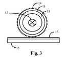
- An example of such a systemis shown in FIG. 3 .
- the “rolling mask”may be in the form of a glass (quartz) frame in the shape of hollow cylinder 11 , which contains a light source 12 .
- An elastomeric film 13 laminated on the outer surface of the cylinder 11has a nanopattern 14 fabricated in accordance with the desired pattern.
- the nanopattern 14can be designed to implement phase-shift exposure, and in such case is fabricated as an array of nanogrooves, posts or columns, or may contain features of arbitrary shape.
- the nanopattern on the rolling maskcan have features ranging in size from about 1 nanometer to about 100 microns, preferably from about 10 nanometers to about 1 micron, more preferably from about 50 nanometers to about 500 nanometers.
- the rolling maskcan be used to print features ranging in size from about 1 nanometer to about 1000 nanometers, preferably about 10 nanometers to about 500 nanometers, more preferably about 50 nanometers to about 200 nanometers.
- the rolling maskis brought into a contact with a substrate 15 coated with photosensitive material 16 , such as a photoresist.
- photosensitive material 16such as a photoresist.
- the photosensitive material 16is exposed to radiation from the light source 12 and the pattern on the cylinder is transferred to the photosensitive material at the place where the nanopattern contacts the photosensitive material.
- the substrate 15is translated as the cylinder rotates such that the nanopattern 14 remains in contact with the photosensitive material.
Landscapes
- Physics & Mathematics (AREA)
- General Physics & Mathematics (AREA)
- Exposure And Positioning Against Photoresist Photosensitive Materials (AREA)
- Preparing Plates And Mask In Photomechanical Process (AREA)
Abstract
Description
- This application is a continuation of International Application No. PCT/US2012/057590, filed Sep. 27, 2012 to Boris Kobrin, the entire contents of which are incorporated herein by reference. International Application No. PCT/US2012/057590 claims the benefit of U.S. Provisional Application No. 61/541,947, filed Sep. 20, 2011 to Boris Kobrin, the entire contents of which are incorporated herein by reference.
- Embodiments of the invention relate to photolithography and more particularly to plasmonic lithography which employs metallic nanostructures to manipulate the flow of light and exposure of a photoresist.
- This section describes background subject matter related to the disclosed embodiments of the present invention. There is no intention, either expressed or implied, that the background art discussed in this section legally constitutes prior art.
- Nanostructuring is necessary for many present applications and industries and for new technologies and future advanced products, such as wire grid polarizers for flat panel displays or architectural glass. Nanostructured substrates may be fabricated using techniques such as e-beam direct writing, deep UV lithography, nanosphere lithography, nanoimprint lithography, near-field phase shift lithography, and plasmonic lithography, for example.
- A method of nanopatterning large areas of rigid and flexible substrate materials based on near-field optical lithography is described in International Patent Application Publication WO02009094009 and U.S. Patent Application Publication US20090297989, both of which are incorporated herein by reference. In this technique, a rotatable mask is used to controllably expose a radiation-sensitive material. Typically the rotatable mask comprises a cylinder or cone. The nanopatterning technique makes use of near-field photolithography, where the mask used to pattern the substrate is in contact with the substrate. Near-field photolithography may make use of an elastomeric phase-shifting mask, or may employ surface plasmon technology, where a rotating cylinder surface comprises metal nano holes or nanoparticles. In one implementation such a mask is a near-field phase-shift mask. Near-field phase shift lithography involves exposure of a photoresist layer to ultraviolet (UV) light that passes through an elastomeric phase mask while the mask is in conformal contact with a photoresist. Bringing an elastomeric phase mask into contact with a thin layer of photoresist causes the photoresist to “wet” the surface of the contact surface of the mask. Passing UV light through the mask while it is in contact with the photoresist exposes the photoresist to the distribution of light intensity that develops at the surface of the mask. A phase mask is formed with a depth of relief that is designed to modulate the phase of the transmitted light by it radians. As a result of the phase modulation, a local null in the intensity appears at step edges in the relief pattern formed on the mask. When a positive photoresist is used, exposure through such a mask, followed by development, yields a line of photoresist with a width equal to the characteristic width of the null in intensity. For 365 nm (near UV) light in combination with a conventional photoresist, the width of the null in intensity is approximately 100 nm. A PDMS mask can be used to form a conformal, atomic scale contact with a layer of photoresist. This contact is established spontaneously upon contact, without applied pressure. Generalized adhesion forces guide this process and provide a simple and convenient method of aligning the mask in angle and position in the direction normal to the photoresist surface, to establish perfect contact. There is no physical gap with respect to the photoresist. PDMS is transparent to UV light with wavelengths greater than 300 nm. Passing light from a mercury lamp (where the main spectral lines are at 355-365 nm) through the PDMS while it is in conformal contact with a layer of photoresist exposes the photoresist to the intensity distribution that forms at the mask.
- Another implementation of the mask may include surface plasmon technology in which a patterned metal layer or film is laminated or deposited onto the outer surface of a mask. The metal layer or film has a specific series of through nanoholes. In another embodiment of surface plasmon technology, a layer of metal nanoparticles is deposited on the transparent mask's outer surface, to achieve the surface plasmons by enhanced nanopatterning.
- Unfortunately, it is difficult to laminate or deposit metal onto a mask made of elastomeric materials such as polydimethyl siloxane (PDMS).
- It is within this context that embodiments of the present invention arise.
- Embodiments of the present invention address the problem of plasmonic printing using an elastomeric phase mask. Instead of coating the mask with metal, an underlying transparent substrate is coated with a blanket layer of metal. The metal layer is then coated with a photoresist. A non-metallic phase mask having a pattern of features with a characteristic spatial period is placed against the photoresist. Instead of exposing the photoresist to radiation through a metal mask, the metal layer is then exposed to radiation of a characteristic vacuum wavelength through the transparent substrate. In some embodiments, the resist and metal layer may be exposed to the radiation through the non-metallic mask provided the resist layer is sufficiently thin and/or transparent. Either way, the spatial period of the mask features and the vacuum wavelength of the radiation can be chosen so that the radiation excites surface plasmons at the interface between the metal and the photoresist. The surface plasmons have a characteristic wavelength equal to the period of the surface features.
- The spatial period of variation in the electric field of the surface plasmons is the same as the characteristic wavelength of the surface plasmons. However, the spatial period of variation of intensity of the surface plasmons is proportional to the square of the electric field. As a result the spatial period of variation of intensity distribution produced by two counter-propagating surface plasmons is half the wavelength of the surface plasmons and can equal half the spatial period of features in a mask that launches the counter-propagating surface plasmons.
- Embodiments of the present invention pertain to methods useful in fabrication of near-field optical lithography masks for “Rolling mask” lithography. A cylindrical mask is coated with a polymer, which is patterned with desired features in order to obtain a mask for phase-shift lithography or plasmonic lithography. The polymer (e.g., an elastomer) may be patterned before or after being disposed on the cylinder surface.
FIG. 1 is a schematic diagram illustrating conventional surface plasmon resonant interference nano lithography.FIGS. 2A-2C are a sequence of schematic diagrams illustrating surface plasmon resonant interference nanolithography in accordance with an embodiment of the present invention.FIG. 3 is a schematic diagram illustrating the use of a “Rolling Mask” lithography system to implement plasmon resonant interference nanolithography in accordance with an embodiment of the present invention.- As a preface to the detailed description, it should be noted that, as used in this specification and the appended claims, the singular forms “a”, “an”, and “the” include plural referents, unless the context clearly dictates otherwise.
- In the following Detailed Description, reference is made to the accompanying drawings, which form a part hereof, and in which is shown by way of illustration specific embodiments in which the invention may be practiced. In this regard, directional terminology, such as “top,” “bottom,” “front,” “back,” “leading,” “trailing,” “above”, “below”, etc., is used with reference to the orientation of the figure(s) being described. Because components of embodiments of the present invention can be positioned in a number of different orientations, the directional terminology is used for purposes of illustration and is in no way limiting. It is to be understood that other embodiments may be utilized and structural or logical changes may be made without departing from the scope of the present invention. The following detailed description, therefore, is not to be taken in a limiting sense, and the scope of the present invention is defined by the appended claims.
- Differences between the conventional plasmon resonant nanolithography and embodiments of the present invention may be appreciated by comparing
FIG. 1 toFIGS. 2A-2C .FIG. 1 illustrates conventional plasmon resonant nanolithography process. - As shown in
FIG. 1 , a metallic mask1 with a plurality of features may be fabricated on athin quartz substrate 2. Incident radiation3 of wavelength λ flows through the mask1 and illuminates a photoresist layer4 formed on anunderlying substrate 5, which traditionally is an insulator or semiconductor. In traditional photolithography, this would be a typical diffraction limited exposure and features smaller than approximately λ/2 normally could not be realized. However, the resonant excitation of surface electromagnetic waves on the metallic surfaces (known as surface plasmons) provides a way to get around the diffraction limit. - The basic principle of plasmon resonant interference nanolithography is based on the idea that with the aid of a periodic or non-periodic corrugation or a prism, illumination light can couple with surface plasmons (SPs) to obtain a new state also often referred to as a surface plasmon polariton (SPP), which has high field intensity at a metal surface and can exhibit a much shorter wavelength compared to that of illuminating radiation. The periodicity of the SPP can be smaller than the periodicity Λ of the mask1 that induces excitation of the SPPs. The interference of SPPs propagating in opposite directions can result in a strongly enhanced nanoscale spatial distribution of an electrical field near the metal surface. Because the intensity of the SPP depends on the square of the electrical field the photoresist4 can be subjected to an intensity distribution pattern with an even smaller periodicity than that of SPP waves.
- According to the theory of surface plasmon optics for given materials, the resonant plasmon wavelength λplasmonfor the weak corrugation limit and normal incidence radiation, can be expressed as
- Here, Λ is a spatial periodicity in the mask pattern, ω is the resonant frequency, εmis the frequency-dependent dielectric constant of the metal, εdis the dielectric constant of the adjacent dielectric. For a mask of deep corrugation, the resonant condition of light leaving a structured mask in contact with a substrate varies with the parameters of its structures and the details of the implementation.
- As noted above, the disadvantage of the technique shown in
FIG. 1 is that it is difficult to fabricate a metal mask on many types of mask materials used for phase masks. In particular, it is difficult, indeed it is often impossible, to fabricate a metal mask on a substrate made of an elastomer material such as PDMS. Moreover, a metal layer deposited on nano-scale patterned phase mask may change features dimensions and shape, which is undesirable. Also, metal material covering elastomeric mask makes it less “sticky” and may lead to a slippage problem during a dynamic exposure process. To overcome this disadvantage, embodiments of the present invention utilize a phase mask having a mask pattern that is not made of metal. Another technique used in the past, depositing metal layer on top of photoresist material, is not desirable due to possibility of affecting photoresist sensitivity, surface smoothness and slippage problems outlined above. FIGS. 2A-2C illustrate surface plasmon resonant interference nanolithography in accordance with an embodiment of the present invention. As shown inFIG. 2A , atransparent mask 6 may have a pattern of corrugated features of periodicity Λ and width w. Themask 6 may be made of any suitable transparent material. However, thetransparent mask 6 is not made of metal or other material that supports surface plasmons. In other words, themask 6 is made of a material that does not support surface plasmons. By way of example, and not by way of limitation, themask 6 may be made, e.g., of an elastomer material, such as PDMS. A mask made of an elastomer material is sometimes referred to as a “softmask” or “soft mask”. By way of example, and not by way of limitation, the features may be a pattern of evenly spaced parallel lines. Alternatively, themask 6 may include a two-dimensional pattern of corrugated features.- A thin layer of
photoresist 7 is formed on a blanket layer ofmetal 8 that overlies asubstrate 9. Thephotoresist 7 may be extremely thin, e.g., a few nanometers thick. By way of example, such a thin layer may be deposited by atomic layer deposition (ALD) or chemical vapor deposition (CVD). Alternatively, such layers cold be self-assembled monolayers (SAMs) deposited from a liquid or vapor phase. The photoresist is illuminated by radiation3 of wavelength λ through themask 6. If the photoresist layer is sufficiently thin, the radiation3 may excite surface plasmons10 in opposite directions in the metal layer. As noted above, the surface plasmons have a characteristic spatial period λplasmonthat depends on the material properties of themetal layer 8,photoresist 7, andmask 6 and the spatial period Λ of the features in themask 6. - In an alternative embodiment, the metal layer may8 be illuminated through the
substrate 9 to excite the surface plasmons10 in the metal layer, if the substrate is sufficiently thin and/or transparent to the radiation3. - The surface plasmons10 interfere and produce a pattern of varying electric field E having a characteristic spatial period that can be less than the spatial period Λ of the features in the
mask 6. The corresponding pattern of varying intensity I has a spatial period Λ′ that is about half the spatial period of the plasmonic electric field. The result is a pattern of exposure in thephotoresist 7 characterized by the spatial period Λ′ of the intensity distribution. - By way of example, and not by way of limitation, the incident wavelength may be in a range from about 100 nm to about 500 nm, the mask periodicities may range from about 50 nm to about 1 micrometer, and the linewith of the features in the mask may range from about 25 nm to 500 nanometer.
- The exposed
photoresist 7 may be developed, as shown inFIG. 2B . After developing, the resist has a pattern of features of periodicity Λ′ and width w′ that are significantly smaller than the periodicity Λ and width w of the features in themask 6. The pattern in the photoresist can be transferred to themetal layer 8, by a suitable etch process as shown inFIG. 2C . If desired, the patternedmetal layer 8 may be used as a mask for etching of thesubstrate 9. - Although the foregoing examples have been described in which a mask has periodic features, embodiments of the present invention are not limited to such examples. Alternatively, the mask may have a pattern characterized by arbitrarily-shaped, aperiodic features.
- Furthermore, in alternative embodiments, the
metal layer 8 may be patterned with features (either periodic or aperiodic features) before it is coated with thephotoresist 7. When the metal layer is illuminated by the radiation3 (either through themask 6 or through the substrate9) the combined effects of the features in themask 6 together with the features in themetal layer 8 would determine the pattern of exposure of the resist. - Embodiments of the present invention may be used in conjunction with a type of lithography known as “rolling mask” nanolithography. An example of a “rolling mask” near-field nanolithography system is described in International Patent Application Publication Number WO2009094009, which is incorporated herein by reference. An example of such a system is shown in
FIG. 3 . The “rolling mask” may be in the form of a glass (quartz) frame in the shape ofhollow cylinder 11, which contains alight source 12. Anelastomeric film 13 laminated on the outer surface of thecylinder 11 has ananopattern 14 fabricated in accordance with the desired pattern. Thenanopattern 14 can be designed to implement phase-shift exposure, and in such case is fabricated as an array of nanogrooves, posts or columns, or may contain features of arbitrary shape. The nanopattern on the rolling mask can have features ranging in size from about 1 nanometer to about 100 microns, preferably from about 10 nanometers to about 1 micron, more preferably from about 50 nanometers to about 500 nanometers. The rolling mask can be used to print features ranging in size from about 1 nanometer to about 1000 nanometers, preferably about 10 nanometers to about 500 nanometers, more preferably about 50 nanometers to about 200 nanometers. - The rolling mask is brought into a contact with a
substrate 15 coated withphotosensitive material 16, such as a photoresist. Thephotosensitive material 16 is exposed to radiation from thelight source 12 and the pattern on the cylinder is transferred to the photosensitive material at the place where the nanopattern contacts the photosensitive material. Thesubstrate 15 is translated as the cylinder rotates such that thenanopattern 14 remains in contact with the photosensitive material. - While the above is a complete description of the preferred embodiments of the present invention, it is possible to use various alternatives, modifications, and equivalents. Therefore, the scope of the present invention should be determined not with reference to the above description but should, instead, be determined with reference to the appended claims, along with their full scope of equivalents. Any feature, whether preferred or not, may be combined with any other feature, whether preferred or not. In the claims that follow, the indefinite article “A” or “An” refers to a quantity of one or more of the item following the article, except where expressly stated otherwise. The appended claims are not to be interpreted as including means-plus-function limitations, unless such a limitation is explicitly recited in a given claim using the phrase “means for”. Any element in a claim that does not explicitly state “means for” performing a specified function, is not to be interpreted as a “means” or “step” clause as specified in 35 USC §112, ¶6.
Claims (16)
Priority Applications (1)
| Application Number | Priority Date | Filing Date | Title |
|---|---|---|---|
| US14/229,762US9116430B2 (en) | 2011-09-30 | 2014-03-28 | Plasmonic lithography using phase mask |
Applications Claiming Priority (3)
| Application Number | Priority Date | Filing Date | Title |
|---|---|---|---|
| US201161541947P | 2011-09-30 | 2011-09-30 | |
| PCT/US2012/057590WO2013049367A2 (en) | 2011-09-30 | 2012-09-27 | Plasmonic lithography using phase mask |
| US14/229,762US9116430B2 (en) | 2011-09-30 | 2014-03-28 | Plasmonic lithography using phase mask |
Related Parent Applications (1)
| Application Number | Title | Priority Date | Filing Date |
|---|---|---|---|
| PCT/US2012/057590ContinuationWO2013049367A2 (en) | 2011-09-30 | 2012-09-27 | Plasmonic lithography using phase mask |
Publications (2)
| Publication Number | Publication Date |
|---|---|
| US20150177619A1true US20150177619A1 (en) | 2015-06-25 |
| US9116430B2 US9116430B2 (en) | 2015-08-25 |
Family
ID=47996741
Family Applications (1)
| Application Number | Title | Priority Date | Filing Date |
|---|---|---|---|
| US14/229,762ActiveUS9116430B2 (en) | 2011-09-30 | 2014-03-28 | Plasmonic lithography using phase mask |
Country Status (2)
| Country | Link |
|---|---|
| US (1) | US9116430B2 (en) |
| WO (1) | WO2013049367A2 (en) |
Cited By (5)
| Publication number | Priority date | Publication date | Assignee | Title |
|---|---|---|---|---|
| EP3312674A1 (en)* | 2016-10-21 | 2018-04-25 | Thomson Licensing | A photolithography device for generating pattern on a photoresist substrate |
| US11061245B2 (en) | 2016-03-24 | 2021-07-13 | Interdigital Ce Patent Holdings | Device for forming nanojet beams in a near zone, from incident electromagnetic waves |
| US11079523B2 (en) | 2016-10-21 | 2021-08-03 | Interdigital Ce Patent Holdings | Device and method for shielding at least one sub-wavelength-scale object from an incident electromagnetic wave |
| US11275252B2 (en) | 2016-10-21 | 2022-03-15 | Interdigital Ce Patent Holdings | Device for forming at least one tilted focused beam in the near zone, from incident electromagnetic waves |
| US11396474B2 (en) | 2017-04-07 | 2022-07-26 | Interdigital Ce Patent Holdings, Sas | Method for manufacturing a device for forming at least one focused beam in a near zone |
Families Citing this family (13)
| Publication number | Priority date | Publication date | Assignee | Title |
|---|---|---|---|---|
| US10807119B2 (en) | 2013-05-17 | 2020-10-20 | Birmingham Technologies, Inc. | Electrospray pinning of nanograined depositions |
| US10559864B2 (en) | 2014-02-13 | 2020-02-11 | Birmingham Technologies, Inc. | Nanofluid contact potential difference battery |
| WO2015183243A1 (en) | 2014-05-27 | 2015-12-03 | Rolith, Inc. | Anti-counterfeiting features and methods of fabrication and detection |
| WO2016089308A1 (en)* | 2014-12-02 | 2016-06-09 | Agency for Science,Technology and Research | Photolithography methods |
| CN105069194B (en)* | 2015-07-20 | 2017-12-26 | 中国科学院长春光学精密机械与物理研究所 | A kind of optimization method of the photoetching attenuation type mask based on genetic algorithm |
| US11101421B2 (en) | 2019-02-25 | 2021-08-24 | Birmingham Technologies, Inc. | Nano-scale energy conversion device |
| US11244816B2 (en) | 2019-02-25 | 2022-02-08 | Birmingham Technologies, Inc. | Method of manufacturing and operating nano-scale energy conversion device |
| US10950706B2 (en) | 2019-02-25 | 2021-03-16 | Birmingham Technologies, Inc. | Nano-scale energy conversion device |
| US11046578B2 (en) | 2019-05-20 | 2021-06-29 | Birmingham Technologies, Inc. | Single-nozzle apparatus for engineered nano-scale electrospray depositions |
| US11124864B2 (en) | 2019-05-20 | 2021-09-21 | Birmingham Technologies, Inc. | Method of fabricating nano-structures with engineered nano-scale electrospray depositions |
| US11649525B2 (en) | 2020-05-01 | 2023-05-16 | Birmingham Technologies, Inc. | Single electron transistor (SET), circuit containing set and energy harvesting device, and fabrication method |
| US11417506B1 (en) | 2020-10-15 | 2022-08-16 | Birmingham Technologies, Inc. | Apparatus including thermal energy harvesting thermionic device integrated with electronics, and related systems and methods |
| US11616186B1 (en) | 2021-06-28 | 2023-03-28 | Birmingham Technologies, Inc. | Thermal-transfer apparatus including thermionic devices, and related methods |
Citations (2)
| Publication number | Priority date | Publication date | Assignee | Title |
|---|---|---|---|---|
| US4767723A (en)* | 1987-10-30 | 1988-08-30 | International Business Machines Corporation | Process for making self-aligning thin film transistors |
| US8450160B2 (en)* | 2010-12-10 | 2013-05-28 | Samsung Display Co., Ltd. | Flattening method of a substrate |
Family Cites Families (13)
| Publication number | Priority date | Publication date | Assignee | Title |
|---|---|---|---|---|
| JPS59200419A (en)* | 1983-04-28 | 1984-11-13 | Toshiba Corp | Large area exposure apparatus |
| US5043244A (en)* | 1990-09-10 | 1991-08-27 | E. I. Du Pont De Nemours And Company | Process for defined etching of substrates |
| JP4236081B2 (en)* | 2001-10-16 | 2009-03-11 | 大日本印刷株式会社 | Method for producing pattern forming body |
| JP4194516B2 (en)* | 2003-06-24 | 2008-12-10 | キヤノン株式会社 | Exposure method, exposure mask and device manufacturing method |
| US7541115B1 (en)* | 2004-11-15 | 2009-06-02 | Kla-Tencor Technologies Corporation | Use of calcium fluoride substrate for lithography masks |
| US20070048628A1 (en)* | 2005-09-01 | 2007-03-01 | Mackey Jeffrey L | Plasmonic array for maskless lithography |
| WO2008153674A1 (en) | 2007-06-09 | 2008-12-18 | Boris Kobrin | Method and apparatus for anisotropic etching |
| US8182982B2 (en) | 2008-04-19 | 2012-05-22 | Rolith Inc | Method and device for patterning a disk |
| US8518633B2 (en) | 2008-01-22 | 2013-08-27 | Rolith Inc. | Large area nanopatterning method and apparatus |
| EP2238608A4 (en)* | 2008-01-22 | 2012-02-22 | Rolith Inc | Large area nanopatterning method and apparatus |
| US8192920B2 (en) | 2008-04-26 | 2012-06-05 | Rolith Inc. | Lithography method |
| US8334217B2 (en) | 2008-06-09 | 2012-12-18 | Rolith Inc. | Material deposition over template |
| US8318386B2 (en) | 2008-08-07 | 2012-11-27 | Rolith Inc. | Fabrication of nanostructured devices |
- 2012
- 2012-09-27WOPCT/US2012/057590patent/WO2013049367A2/enactiveApplication Filing
- 2014
- 2014-03-28USUS14/229,762patent/US9116430B2/enactiveActive
Patent Citations (2)
| Publication number | Priority date | Publication date | Assignee | Title |
|---|---|---|---|---|
| US4767723A (en)* | 1987-10-30 | 1988-08-30 | International Business Machines Corporation | Process for making self-aligning thin film transistors |
| US8450160B2 (en)* | 2010-12-10 | 2013-05-28 | Samsung Display Co., Ltd. | Flattening method of a substrate |
Cited By (8)
| Publication number | Priority date | Publication date | Assignee | Title |
|---|---|---|---|---|
| US11061245B2 (en) | 2016-03-24 | 2021-07-13 | Interdigital Ce Patent Holdings | Device for forming nanojet beams in a near zone, from incident electromagnetic waves |
| US11163175B2 (en) | 2016-03-24 | 2021-11-02 | Interdigital Ce Patent Holdings | Device for forming a field intensity pattern in the near zone, from incident electromagnetic waves |
| EP3312674A1 (en)* | 2016-10-21 | 2018-04-25 | Thomson Licensing | A photolithography device for generating pattern on a photoresist substrate |
| WO2018073427A1 (en)* | 2016-10-21 | 2018-04-26 | Thomson Licensing | A photolithography device for generating pattern on a photoresist substrate |
| US10678127B2 (en) | 2016-10-21 | 2020-06-09 | Interdigital Ce Patent Holdings, Sas | Photolithography device for generating pattern on a photoresist substrate |
| US11079523B2 (en) | 2016-10-21 | 2021-08-03 | Interdigital Ce Patent Holdings | Device and method for shielding at least one sub-wavelength-scale object from an incident electromagnetic wave |
| US11275252B2 (en) | 2016-10-21 | 2022-03-15 | Interdigital Ce Patent Holdings | Device for forming at least one tilted focused beam in the near zone, from incident electromagnetic waves |
| US11396474B2 (en) | 2017-04-07 | 2022-07-26 | Interdigital Ce Patent Holdings, Sas | Method for manufacturing a device for forming at least one focused beam in a near zone |
Also Published As
| Publication number | Publication date |
|---|---|
| US9116430B2 (en) | 2015-08-25 |
| WO2013049367A3 (en) | 2013-05-23 |
| WO2013049367A2 (en) | 2013-04-04 |
Similar Documents
| Publication | Publication Date | Title |
|---|---|---|
| US9116430B2 (en) | Plasmonic lithography using phase mask | |
| Henzie et al. | Multiscale patterning of plasmonic metamaterials | |
| US9465296B2 (en) | Nanopatterning method and apparatus | |
| US9069244B2 (en) | Mask for near-field lithography and fabrication the same | |
| US8518633B2 (en) | Large area nanopatterning method and apparatus | |
| JP5102879B2 (en) | Large-area nanopattern forming method and apparatus | |
| US20100035163A1 (en) | Fabrication of nanostructured devices | |
| CA2786489A1 (en) | Nanopatterning method and apparatus | |
| Blaikie et al. | Super-resolution near-field lithography using planar silver lenses: A review of recent developments | |
| US20120282554A1 (en) | Large area nanopatterning method and apparatus | |
| CN103454866A (en) | Photoetching imaging equipment and photoetching imaging method based on surface plasma wave illumination | |
| CN109669323B (en) | A method for realizing large-area super-resolution lithography based on resonant cavity structure | |
| Kim et al. | Surface plasmon-assisted nano-lithography with a perfect contact aluminum mask of a hexagonal dot array | |
| Li et al. | Ag dots array fabricated using laser interference technique for biosensing | |
| CN109116687B (en) | A light-generating device for super-resolution lithography | |
| Skinner et al. | Large-area subwavelength aperture arrays fabricated using nanoimprint lithography | |
| US20140234780A1 (en) | Lithography with reduced feature pitch using rotating mask techniques | |
| Yang et al. | Fabrication of Ag nanodot array over large area for surface-enhanced Raman scattering using hybrid nanoimprint mold made from AAO template | |
| Kim et al. | Comparative study of nanolithography based on extraordinary and diffracted optical transmissions | |
| Dhima et al. | Nanoimprint combination techniques | |
| CN109901362A (en) | Secondary imaging optical lithography method and apparatus | |
| Xiong et al. | 193 nm interference nanolithography based on SPP | |
| Kim et al. | Distortion analysis of periodic ring patterns fabrication using surface plasmon interference lithography with an Al hexagonal grating structure on glass | |
| Bourgin et al. | Periodic sub-100nm structures fabricated by proximity i-line mask-aligner lithography (and self-aligned double patterning) | |
| Yoshida et al. | Fluorescence imprint alignment using additive-type inclination moiré fringes |
Legal Events
| Date | Code | Title | Description |
|---|---|---|---|
| AS | Assignment | Owner name:ROLITH, INC., CALIFORNIA Free format text:ASSIGNMENT OF ASSIGNORS INTEREST;ASSIGNORS:KOBRIN, BORIS;BARNARD, EDWARD;SIGNING DATES FROM 20150123 TO 20150221;REEL/FRAME:035008/0876 | |
| STCF | Information on status: patent grant | Free format text:PATENTED CASE | |
| AS | Assignment | Owner name:METAMATERIAL TECHNOLOGIES USA, INC., CALIFORNIA Free format text:ASSIGNMENT OF ASSIGNORS INTEREST;ASSIGNOR:ROLITH, INC.;REEL/FRAME:038945/0136 Effective date:20160514 | |
| MAFP | Maintenance fee payment | Free format text:PAYMENT OF MAINTENANCE FEE, 4TH YR, SMALL ENTITY (ORIGINAL EVENT CODE: M2551); ENTITY STATUS OF PATENT OWNER: SMALL ENTITY Year of fee payment:4 | |
| AS | Assignment | Owner name:BDC CAPITAL INC., CANADA Free format text:SECURITY INTEREST;ASSIGNOR:METAMATERIAL TECHNOLOGIES USA, INC.;REEL/FRAME:052315/0029 Effective date:20200403 | |
| AS | Assignment | Owner name:METAMATERIAL TECHNOLOGIES USA, INC., CALIFORNIA Free format text:RELEASE BY SECURED PARTY;ASSIGNOR:BDC CAPITAL INC.;REEL/FRAME:056522/0648 Effective date:20210611 | |
| MAFP | Maintenance fee payment | Free format text:PAYMENT OF MAINTENANCE FEE, 8TH YR, SMALL ENTITY (ORIGINAL EVENT CODE: M2552); ENTITY STATUS OF PATENT OWNER: SMALL ENTITY Year of fee payment:8 | |
| AS | Assignment | Owner name:E INK CORPORATION, MASSACHUSETTS Free format text:COURT APPOINTMENT;ASSIGNOR:CHRISTINA LOVATO, CHAPTER 7 TRUSTEE OF THE BANKRUPTCY ESTATE OF META MATERIALS INC.;REEL/FRAME:070871/0818 Effective date:20250417 | |
| FEPP | Fee payment procedure | Free format text:ENTITY STATUS SET TO UNDISCOUNTED (ORIGINAL EVENT CODE: BIG.); ENTITY STATUS OF PATENT OWNER: LARGE ENTITY |