US20150145048A1 - Structure and method for forming cmos with nfet and pfet having different channel materials - Google Patents
Structure and method for forming cmos with nfet and pfet having different channel materialsDownload PDFInfo
- Publication number
- US20150145048A1 US20150145048A1US14/088,025US201314088025AUS2015145048A1US 20150145048 A1US20150145048 A1US 20150145048A1US 201314088025 AUS201314088025 AUS 201314088025AUS 2015145048 A1US2015145048 A1US 2015145048A1
- Authority
- US
- United States
- Prior art keywords
- layer
- semiconductor structure
- semiconductor
- forming
- gap
- Prior art date
- Legal status (The legal status is an assumption and is not a legal conclusion. Google has not performed a legal analysis and makes no representation as to the accuracy of the status listed.)
- Granted
Links
Images


Classifications
- H01L27/1211—
- H—ELECTRICITY
- H10—SEMICONDUCTOR DEVICES; ELECTRIC SOLID-STATE DEVICES NOT OTHERWISE PROVIDED FOR
- H10D—INORGANIC ELECTRIC SEMICONDUCTOR DEVICES
- H10D86/00—Integrated devices formed in or on insulating or conducting substrates, e.g. formed in silicon-on-insulator [SOI] substrates or on stainless steel or glass substrates
- H10D86/201—Integrated devices formed in or on insulating or conducting substrates, e.g. formed in silicon-on-insulator [SOI] substrates or on stainless steel or glass substrates the substrates comprising an insulating layer on a semiconductor body, e.g. SOI
- H10D86/215—Integrated devices formed in or on insulating or conducting substrates, e.g. formed in silicon-on-insulator [SOI] substrates or on stainless steel or glass substrates the substrates comprising an insulating layer on a semiconductor body, e.g. SOI comprising FinFETs
- H01L21/823821—
- H01L21/845—
- H—ELECTRICITY
- H10—SEMICONDUCTOR DEVICES; ELECTRIC SOLID-STATE DEVICES NOT OTHERWISE PROVIDED FOR
- H10D—INORGANIC ELECTRIC SEMICONDUCTOR DEVICES
- H10D84/00—Integrated devices formed in or on semiconductor substrates that comprise only semiconducting layers, e.g. on Si wafers or on GaAs-on-Si wafers
- H10D84/01—Manufacture or treatment
- H10D84/0123—Integrating together multiple components covered by H10D12/00 or H10D30/00, e.g. integrating multiple IGBTs
- H10D84/0126—Integrating together multiple components covered by H10D12/00 or H10D30/00, e.g. integrating multiple IGBTs the components including insulated gates, e.g. IGFETs
- H10D84/0165—Integrating together multiple components covered by H10D12/00 or H10D30/00, e.g. integrating multiple IGBTs the components including insulated gates, e.g. IGFETs the components including complementary IGFETs, e.g. CMOS devices
- H10D84/0193—Integrating together multiple components covered by H10D12/00 or H10D30/00, e.g. integrating multiple IGBTs the components including insulated gates, e.g. IGFETs the components including complementary IGFETs, e.g. CMOS devices the components including FinFETs
- H—ELECTRICITY
- H10—SEMICONDUCTOR DEVICES; ELECTRIC SOLID-STATE DEVICES NOT OTHERWISE PROVIDED FOR
- H10D—INORGANIC ELECTRIC SEMICONDUCTOR DEVICES
- H10D84/00—Integrated devices formed in or on semiconductor substrates that comprise only semiconducting layers, e.g. on Si wafers or on GaAs-on-Si wafers
- H10D84/01—Manufacture or treatment
- H10D84/02—Manufacture or treatment characterised by using material-based technologies
- H10D84/03—Manufacture or treatment characterised by using material-based technologies using Group IV technology, e.g. silicon technology or silicon-carbide [SiC] technology
- H10D84/038—Manufacture or treatment characterised by using material-based technologies using Group IV technology, e.g. silicon technology or silicon-carbide [SiC] technology using silicon technology, e.g. SiGe
- H—ELECTRICITY
- H10—SEMICONDUCTOR DEVICES; ELECTRIC SOLID-STATE DEVICES NOT OTHERWISE PROVIDED FOR
- H10D—INORGANIC ELECTRIC SEMICONDUCTOR DEVICES
- H10D84/00—Integrated devices formed in or on semiconductor substrates that comprise only semiconducting layers, e.g. on Si wafers or on GaAs-on-Si wafers
- H10D84/80—Integrated devices formed in or on semiconductor substrates that comprise only semiconducting layers, e.g. on Si wafers or on GaAs-on-Si wafers characterised by the integration of at least one component covered by groups H10D12/00 or H10D30/00, e.g. integration of IGFETs
- H10D84/82—Integrated devices formed in or on semiconductor substrates that comprise only semiconducting layers, e.g. on Si wafers or on GaAs-on-Si wafers characterised by the integration of at least one component covered by groups H10D12/00 or H10D30/00, e.g. integration of IGFETs of only field-effect components
- H10D84/83—Integrated devices formed in or on semiconductor substrates that comprise only semiconducting layers, e.g. on Si wafers or on GaAs-on-Si wafers characterised by the integration of at least one component covered by groups H10D12/00 or H10D30/00, e.g. integration of IGFETs of only field-effect components of only insulated-gate FETs [IGFET]
- H10D84/8311—Integrated devices formed in or on semiconductor substrates that comprise only semiconducting layers, e.g. on Si wafers or on GaAs-on-Si wafers characterised by the integration of at least one component covered by groups H10D12/00 or H10D30/00, e.g. integration of IGFETs of only field-effect components of only insulated-gate FETs [IGFET] the IGFETs characterised by having different channel structures
- H—ELECTRICITY
- H10—SEMICONDUCTOR DEVICES; ELECTRIC SOLID-STATE DEVICES NOT OTHERWISE PROVIDED FOR
- H10D—INORGANIC ELECTRIC SEMICONDUCTOR DEVICES
- H10D84/00—Integrated devices formed in or on semiconductor substrates that comprise only semiconducting layers, e.g. on Si wafers or on GaAs-on-Si wafers
- H10D84/80—Integrated devices formed in or on semiconductor substrates that comprise only semiconducting layers, e.g. on Si wafers or on GaAs-on-Si wafers characterised by the integration of at least one component covered by groups H10D12/00 or H10D30/00, e.g. integration of IGFETs
- H10D84/82—Integrated devices formed in or on semiconductor substrates that comprise only semiconducting layers, e.g. on Si wafers or on GaAs-on-Si wafers characterised by the integration of at least one component covered by groups H10D12/00 or H10D30/00, e.g. integration of IGFETs of only field-effect components
- H10D84/83—Integrated devices formed in or on semiconductor substrates that comprise only semiconducting layers, e.g. on Si wafers or on GaAs-on-Si wafers characterised by the integration of at least one component covered by groups H10D12/00 or H10D30/00, e.g. integration of IGFETs of only field-effect components of only insulated-gate FETs [IGFET]
- H10D84/85—Complementary IGFETs, e.g. CMOS
- H10D84/853—Complementary IGFETs, e.g. CMOS comprising FinFETs
- H—ELECTRICITY
- H10—SEMICONDUCTOR DEVICES; ELECTRIC SOLID-STATE DEVICES NOT OTHERWISE PROVIDED FOR
- H10D—INORGANIC ELECTRIC SEMICONDUCTOR DEVICES
- H10D86/00—Integrated devices formed in or on insulating or conducting substrates, e.g. formed in silicon-on-insulator [SOI] substrates or on stainless steel or glass substrates
- H10D86/01—Manufacture or treatment
- H10D86/011—Manufacture or treatment comprising FinFETs
Definitions
- the present inventionrelates generally to semiconductor fabrication, and more particularly, to formation of CMOS field effect transistor structures.
- ICsemiconductor integrated circuit
- functional densityi.e., the number of interconnected devices per chip area
- geometry sizei.e., the smallest component (or line) that can be created using a fabrication process
- This scaling down processgenerally provides benefits by increasing production efficiency and lowering associated costs.
- Such scaling downhas also increased the complexity of processing and manufacturing ICs and, for these advances to be realized, similar developments in IC manufacturing are needed.
- the FinFET devicemay be a complementary metal-oxide-semiconductor (CMOS) device comprising a P-type metal-oxide-semiconductor (PMOS) FinFET device and a N-type metal-oxide-semiconductor (NMOS) FinFET device.
- CMOS technologyis used in a wide variety of circuit designs. It is therefore desirable to have improvements in the fabrication of CMOS finFET semiconductor structures.
- embodiments of the present inventionprovide a method of forming a semiconductor structure, comprising: forming a first semiconductor layer; forming a second semiconductor layer; forming a gap in the semiconductor structure to form an NFET side of the semiconductor structure, and a PFET side of the semiconductor structure, wherein the NFET side is separated from the PFET side by the gap; removing the second semiconductor layer from the NFET side of the semiconductor structure; and forming a plurality of fins in the first semiconductor layer on the NFET side and forming a plurality of fins in the second semiconductor layer on the PFET side.
- embodiments of the present inventionprovide a method of forming a semiconductor structure, comprising: forming a recess on a PFET side of a silicon-on-insulator (SOI) layer disposed on a buried oxide (BOX) layer, wherein the BOX layer is disposed on a semiconductor substrate, and wherein the recess extends partially into the SOI layer, thereby forming a recessed portion of the SOI layer on the PFET side of the SOI layer, and a non-recessed portion on an NFET side of the SOI layer; forming a gap in the semiconductor structure, wherein the NFET side is separated from the PFET side by the gap; growing an epitaxial silicon germanium (SiGe) layer on the recessed portion of the SOI layer; converting the SOI layer on the PFET side to SiGe; and forming a plurality of fins in the SOI layer on the NFET side and forming a plurality of fins in the SiGe layer on
- embodiments of the present inventionprovide a semiconductor structure, comprising: a semiconductor substrate comprising a first semiconductor material and a second semiconductor material; a first set of fins comprised of the first semiconductor material, disposed on a first side of the semiconductor structure; a second set of fins comprised of the second semiconductor material, disposed on a second side of the semiconductor structure; an insulator region disposed between the first side of the semiconductor structure and the second side of the semiconductor structure, wherein the insulator region has a width ranging from about 10 nanometers to about 50 nanometers.
- cross-sectional viewsmay be in the form of “slices”, or “near-sighted” cross-sectional views, omitting certain background lines which would otherwise be visible in a “true” cross-sectional view, for illustrative clarity.
- FIG. 1Ais a semiconductor structure at a starting point for embodiments of the present invention.
- FIG. 1Bis a semiconductor structure at a starting point for alternative embodiments of the present invention.
- FIG. 2is a semiconductor structure after subsequent process steps of depositing and patterning a resist layer.
- FIG. 3is a semiconductor structure after a subsequent process step of forming a gap in the semiconductor structure.
- FIG. 4Ais a semiconductor structure after subsequent process steps of removing the resist layer, and filling the gap with an insulator material.
- FIG. 4Bis a semiconductor structure after subsequent process steps of removing the resist layer, and filling the gap with an insulator material in accordance with an alternative embodiment.
- FIG. 5is a semiconductor structure after subsequent process steps of removing the nitride layer and SiGe layer from the NFET side of the semiconductor structure.
- FIG. 6is a semiconductor structure after subsequent process steps of replenishing the nitride layer on the NFET side of the semiconductor structure and planarizing the semiconductor structure.
- FIG. 7is a semiconductor structure after a subsequent process step of converting the SOI layer on the PFET side into SiGe.
- FIG. 8is a semiconductor structure after a subsequent process step of recessing the SiGe region on the PFET side.
- FIG. 9is a semiconductor structure in accordance with embodiments of the present invention, after a subsequent process step of fin formation.
- FIG. 10is a semiconductor structure after a subsequent process step of converting the SOI layer on the PFET side into SiGe, in accordance with alternative embodiments.
- FIG. 11is a semiconductor structure after subsequent process steps of removing the nitride and thermal oxide.
- FIG. 12is a semiconductor structure at a starting point for alternative embodiments of the present invention.
- FIG. 13is a semiconductor structure after a subsequent process step of epitaxial SiGe growth on the PFET side of the semiconductor structure.
- FIG. 14is a semiconductor structure after subsequent process steps of depositing and patterning a resist layer, and forming a gap in the semiconductor structure.
- FIG. 15is a semiconductor structure after a subsequent process step of converting the SOI layer on the PFET side into SiGe.
- FIG. 16is a semiconductor structure after a subsequent process step of depositing an insulator material into the gap.
- FIG. 17is a semiconductor structure in accordance with alternative embodiments of the present invention, after a subsequent process step of fin formation.
- FIG. 18is a flowchart indicating process steps for embodiments of the present invention.
- FIG. 19is a flowchart indicating process steps for alternative embodiments of the present invention.
- Embodiments of the present inventionprovide an improved structure and method for forming CMOS field effect transistors.
- silicon germaniumSiGe
- SiGesilicon germanium
- the NFET finsare comprised of silicon and the PFET fins are comprised of silicon germanium.
- FIG. 1Ais a semiconductor structure 100 at a starting point for embodiments of the present invention.
- a bulk substrate 102forms the base of semiconductor structure 100 .
- Bulk substrate 102may be made from any of several known semiconductor materials such as, for example, silicon, germanium, a silicon-germanium alloy, a silicon carbon alloy, a silicon-germanium-carbon alloy, gallium arsenide, indium arsenide, indium phosphide, III-V compound semiconductor materials, II-VI compound semiconductor materials, organic semiconductor materials, and other compound semiconductor materials.
- An insulator layer 104is disposed on the bulk substrate 102 .
- insulator layer 104may be comprised of oxide, such as silicon oxide, and may be referred to as a buried oxide (BOX) layer.
- a first semiconductor layer 106is disposed on the insulator layer 104 .
- first semiconductor layer 106is comprised of silicon, forming a so-called silicon-on-insulator (SOI) structure.
- SOIsilicon-on-insulator
- layer 106may be referred to as a silicon-on-insulator (SOI) layer.
- a second semiconductor layer 108is disposed on the first semiconductor layer 106 .
- second semiconductor layer 108is comprised silicon germanium (SiGe).
- layer 108may be referred to as a SiGe layer.
- the concentration of germanium in layer 108may range from about 30 atomic percent to about 50 atomic percent, although germanium concentration less than 30% or greater than 50% may also be possible.
- hardmask layer 110Disposed on SiGe layer 108 is a hardmask layer 110 .
- hardmask layer 110may comprise a nitride, such as silicon nitride.
- the second semiconductor layer 108is comprised of germanium.
- the second semiconductor layer 108may be comprised of a different semiconductor material, so long as it differs from the material of first semiconductor layer 106 .
- FIG. 1Bis a semiconductor structure 101 at a starting point for embodiments of the present invention.
- a “bulk” structureis used, where bulk substrate 102 forms the first semiconductor layer, and second semiconductor layer 108 is disposed on the bulk substrate.
- FIG. 2is a semiconductor structure 200 after subsequent process steps of depositing and patterning a resist layer 212 .
- similar elementsmay be referred to by similar numbers in various figures (FIGs) of the drawing, in which case typically the last two significant digits may be the same.
- bulk substrate 202 of FIG. 2is similar to bulk substrate 102 of FIG. 1 .
- the resist layer 212is patterned utilizing a lithographic mask 214 , such that gap 224 is formed in the resist.
- the gap 224has a width W. In embodiments, the width W ranges from about 10 nanometers to about 50 nanometers.
- resist layer 212comprises a hybrid resist, which has a property of forming a narrow development range adjacent to the edge of a mask.
- the hybrid resistcomprises a combination of positive and negative photoresists and is described in detail in U.S. Pat. No. 6,114,082, filed Sep. 19, 1996, which is hereby incorporated by reference herein in its entirety.
- FIG. 3is a semiconductor structure 300 after a subsequent process step of forming a gap 324 in the semiconductor structure.
- the gap 324is formed by an anisotropic etch process, such as a reactive ion etch (RIE). This forms a cavity in the semiconductor structure disposed underneath the gap in the hybrid resist layer, thereby forming gap 324 , wherein the cavity (gap) extends to the BOX layer 304 .
- the gap 324has a width W. In embodiments, the width W ranges from about 10 nanometers to about 50 nanometers.
- the etch processstops on the insulator layer 304 .
- the gap 324thus separates the structure 300 into two sides: NFET side 320 and PFET side 322 .
- an NFETN-type field effect transistor
- a PFETP-type field effect transistor
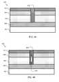
- FIG. 4Ais a semiconductor structure 400 after subsequent process steps of removing the resist layer (compare with 312 of FIG. 3 ), and filling the gap with an insulator material 416 .
- insulator material 416may be comprised of an oxide, such as silicon oxide, and may include a flowable oxide, or LPCVD (low pressure chemical vapor deposition) oxide.
- FIG. 4Bis a semiconductor structure 401 similar to 400 of FIG. 4A , except that the gap is filled with a conformal nitride 418 , such as a silicon nitride, which is deposited in the gap, and then pinched off at the top. In some cases, a void 419 may be present in the conformal nitride 418 .
- a conformal nitride 418such as a silicon nitride
- FIG. 5is a semiconductor structure 500 after subsequent process steps (following from FIG. 4A ) of removing the nitride layer and SiGe layer from the NFET side 520 of the semiconductor structure 500 .
- the removalmay be accomplished via industry-standard lithographic and etching techniques.
- FIG. 6is a semiconductor structure 600 after subsequent process steps of replenishing the nitride layer 610 A on the NFET side 620 of the semiconductor structure and planarizing the semiconductor structure 600 .
- the semiconductor structure 600may be planarized after deposition of nitride layer 610 A.
- the planarizationmay be performed with a chemical mechanical polish (CMP) process.
- CMPchemical mechanical polish
- FIG. 7is a semiconductor structure 700 after a subsequent process step of converting the SOI layer on the PFET side ( 606 B of FIG. 6 ) into SiGe, creating larger SiGe region 708 (as compared with 608 of FIG. 6 ) on the PFET side 722 .
- the conversion processincludes thermal mixing, where the semiconductor structure 700 is annealed to disperse SiGe from the layer ( 608 of FIG. 6 ) into the SOI layer on the PFET side ( 606 B of FIG. 6 ).
- the annealmay be performed at a process temperature ranging from about 1000 degrees Celsius to about 1100 degrees Celsius for a duration ranging from about 1 minute to about 70 minutes.
- the anneal (conversion) stepcan be omitted.
- FIG. 8is a semiconductor structure 800 after a subsequent process step of recessing the SiGe region on the PFET side.
- a nitride etch backis performed to expose the SiGe region 808 on the PFET side 822 .
- Nitride region 810remains on NFET side 820 since the starting thickness on that side is greater than on the PFET side 822 (compare the thickness of nitride region 710 A and 710 B in FIG. 7 ).
- the thickness of the SiGe region 808may be made to be the same as the thickness of SOI layer 806 .
- FIG. 9is a semiconductor structure 900 in accordance with embodiments of the present invention, after a subsequent process step of fin formation.
- the remaining nitride region ( 810 of FIG. 8 )is removed, and the insulator region 916 may be recessed to a desired level.
- the insulator region 916has width W. In some embodiments, the width W ranges from about 10 nanometers to about 50 nanometers.
- a first set of finsare formed on NFET side 920 .
- the NFET finsare indicated generally as 926 .
- a second set of finsare formed on PFET side 922 .
- the PFET finsare indicated generally as 928 .
- the finsmay be formed by any suitable technique, such as a sidewall image transfer (SIT) process.
- SITsidewall image transfer
- the fins 926 on NFET side 920are comprised of silicon, while the fins 928 on PFET side 922 are formed of silicon germanium (SiGe).
- the channels of each transistorare contained within the fins. Silicon has better carrier mobility for NFET transistors, and SiGe has better carrier mobility for PFET transistors.
- the embodiment of FIG. 9provides improved performance for each transistor of the CMOS pair, while also enabling closer placement of the finFETs with dissimilar channel materials, which increases circuit density and reduces lengths of metallization wiring, thereby improving overall performance of an integrated circuit utilizing CMOS technology.
- FIG. 10is a semiconductor structure 1000 after a subsequent process step of converting the SOI layer on the PFET side into SiGe, in accordance with alternative embodiments.
- Semiconductor structure 1000follows from semiconductor structure 600 of FIG. 6 .
- the nitrideis stripped, exposing the SiGe layer 608 .
- a thermal oxidation processis then performed, forming oxide region 1030 .
- the thermal oxidation processtakes place at an elevated temperature, such that germanium from the SiGe layer 608 diffuses into the SOI layer 606 B.
- the result, shown in FIG. 10is that layer 1008 is comprised of SiGe.
- the thermal oxidation processactually consumes some of layer 1008 , effectively “lowering” layer 1008 .
- a desired thickness of layer 1008is achieved.
- the thickness of layer 1008may be similar to the thickness of layer 1006 . In other embodiments, the thickness of layer 1008 may be different than the thickness of layer 1006 .
- the thickness of layers 1006 and 1008determine the fin height for the NFET and PFET respectively.
- FIG. 11is a semiconductor structure 1100 after subsequent process steps of removing the nitride and thermal oxide.
- Semiconductor structure 1100comprises SOI layer 1106 on the NFET side 1120 , and SiGe layer 1108 on the PFET side 1122 . From this point forward, the fins are formed, resulting in a structure similar to structure 900 of FIG. 9 .
- FIG. 12is a semiconductor structure 1200 at a starting point for alternative embodiments of the present invention.
- Semiconductor structure 1200is a silicon-on-insulator structure comprising bulk semiconductor substrate 1202 .
- An insulator layer 1204is disposed on the bulk semiconductor substrate 1202 .
- a silicon layer 1206is disposed on the insulator layer 1204 .
- Silicon layer 1206may be referred to as a SOI layer.
- a nitride layer 1210is disposed on the SOI layer 1206 .
- a recessis formed on the PFET side 1222 of the structure 1200 , while the nitride layer 1210 is preserved on the NFET side 1220 of the structure.
- the recessing of the PFET side 1222 of structure 1200may be performed using industry-standard patterning and etching techniques.
- the recess on the PFET side 1222extends partially into the SOI layer, and as a result of the recess, a recessed portion of the SOI layer, indicated as 1206 B, remains on the PFET side 1222 , while a non-recessed portion of SOI layer 1206 remains on the NFET side 1220 .
- no SiGe layeris deposited initially on the entire structure (as compared with layer 108 in FIG. 1 ).
- the recessed portion of SOI layer 1206 Bhas a thickness T ranging from about 5 nanometers to about 15 nanometers.
- FIG. 13is a semiconductor structure 1300 after a subsequent process step of epitaxial SiGe growth on the PFET side 1322 of the semiconductor structure, resulting in the formation of SiGe layer 1308 .
- the NFET side 1320does not have any SiGe layer, since the nitride layer 1310 prevents exposure of the SOI layer 1306 on the NFET side 1320 .
- the SiGe layer 1308may grow faceted once it exceeds the level of SOI layer 1306 .
- the faceted portion 1308 Fis removed during a subsequent recess of the SiGe layer 1308 .
- FIG. 14is a semiconductor structure 1400 after subsequent process steps of depositing and patterning a resist layer 1412 , and forming a gap 1424 in the semiconductor structure.
- the SiGe layer 1408may be recessed, removing the faceted portion (see 1308 F of FIG. 13 ).
- the amount of recessdetermines the height of the fins for the PFET transistor.
- the recessis such that the level of the top of SiGe layer 1408 is approximately at the same level as the top of SOI region 1406 A.
- the recessis such that the top of SiGe layer 1408 is not at the same level as the top of SOI region 1406 A, but may instead be greater than, or less than the level of the top of SOI region 1406 A. In some cases, it may be desirable to have a different fin height for the PFET than the NFET. This allows device characteristics to be fine tuned.
- resist layer 1412may be a hybrid resist, capable of forming very narrow gaps when lithographically processed using mask 1414 .
- Gap 1424has width W. In embodiments, the width W ranges from about 10 nanometers to about 50 nanometers.
- the gap 1424may be formed with an anisotropic etch process, such as a reactive ion etch (RIE) process. The gap 1424 terminates at the insulator layer 1404 .
- RIEreactive ion etch
- FIG. 15is a semiconductor structure 1500 after a subsequent process step of converting the SOI layer on the PFET side (see 1206 B of FIG. 12 ) into SiGe, thereby forming SiGe layer 1508 on the PFET side 1522 .
- the conversion of the SOI layermay be performed with an anneal process.
- the annealis performed at a process temperature ranging from about 1000 degrees Celsius to about 1100 degrees Celsius for a duration ranging from about 30 seconds to about 20 minutes. The duration may be less than the duration used in the embodiment of FIG. 7 , because the portion of SOI layer that gets converted is fairly thin (in some cases, ranging from about 5 nanometers to about 15 nanometers).
- FIG. 16is a semiconductor structure 1600 after a subsequent process step of depositing an insulator material 1616 into the gap.
- a conformal nitride layersuch as a silicon nitride layer, may be deposited in the gap, similar to as shown in FIG. 4B .
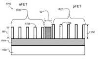
- FIG. 17is a semiconductor structure in accordance with alternative embodiments of the present invention, after a subsequent process step of fin formation.
- Structure 1700is similar to structure 900 of FIG. 9 , except that the height H1 of the fins 1726 on the NFET side 1720 is not equal to the height H2 of the fins 1728 of the PFET side 1722 .
- H1ranges from about 70 nanometers to about 150 nanometers
- H2ranges from about 10 nanometers to about 20 nanometers greater than the H1 value.
- the width W of isolation between the NFET and PFETmay range from about 10 nanometers to about 50 nanometers.
- structure 1700comprises a CMOS pair of an NFET and a PFET, where the fins of the NFET are comprised of a first material, and the fins of the PFET are comprised of a second material, and the devices have a narrow isolation region between them.
- device performancecan be optimized by using a material that enhances carrier mobility for electrons in the NFET, and using a different material that enhances carrier mobility for holes in the PFET.
- the PFET fins 1728are taller than the NFET fins 1726
- the NFET fins 1726may be taller than the PFET fins 1728 .
- FIG. 18is a flowchart 1800 indicating process steps for embodiments of the present invention.
- a silicon germanium (SiGe) layeris formed on a silicon-on-insulator (SOI) structure (see 108 of FIG. 1 ).
- a gapis formed in the semiconductor structure (see 324 of FIG. 3 ).
- SiGeis removed from the NFET side of the structure (see 500 of FIG. 5 ).
- the silicon-on-insulator portion on the PFET sideis converted to SiGe (see 708 of FIG. 7 ).
- finsare formed for an NFET and a PFET (see 900 of FIG. 9 ).
- FIG. 19is a flowchart 1900 indicating process steps for alternative embodiments of the present invention.
- a silicon-on-insulator recessis formed on the PFET side of the structure (see 1200 of FIG. 12 ).
- an epitaxial silicon germanium (SiGe) regionis formed on the PFET side of the structure (see 1308 of FIG. 13 ).
- a gapis formed in the semiconductor structure (see 1424 of FIG. 14 ).
- the silicon-on-insulator portion on the PFET sideis converted to SiGe (see 1508 of FIG. 15 ).
- finsare formed for an NFET and a PFET (see 1700 of FIG. 17 ).
Landscapes
- Metal-Oxide And Bipolar Metal-Oxide Semiconductor Integrated Circuits (AREA)
- Thin Film Transistor (AREA)
Abstract
Description
- The present invention relates generally to semiconductor fabrication, and more particularly, to formation of CMOS field effect transistor structures.
- The semiconductor integrated circuit (IC) industry has experienced rapid growth. In the course of the IC evolution, functional density (i.e., the number of interconnected devices per chip area) has generally increased while geometry size (i.e., the smallest component (or line) that can be created using a fabrication process) has decreased. This scaling down process generally provides benefits by increasing production efficiency and lowering associated costs. Such scaling down has also increased the complexity of processing and manufacturing ICs and, for these advances to be realized, similar developments in IC manufacturing are needed.
- For example, as the semiconductor industry has progressed into nanometer technology process nodes in pursuit of higher device density, higher performance, and lower costs, challenges from both fabrication and design have resulted in the development of fin-type field effect transistor (FinFET) devices. The FinFET device, for example, may be a complementary metal-oxide-semiconductor (CMOS) device comprising a P-type metal-oxide-semiconductor (PMOS) FinFET device and a N-type metal-oxide-semiconductor (NMOS) FinFET device. CMOS technology is used in a wide variety of circuit designs. It is therefore desirable to have improvements in the fabrication of CMOS finFET semiconductor structures.
- In a first aspect, embodiments of the present invention provide a method of forming a semiconductor structure, comprising: forming a first semiconductor layer; forming a second semiconductor layer; forming a gap in the semiconductor structure to form an NFET side of the semiconductor structure, and a PFET side of the semiconductor structure, wherein the NFET side is separated from the PFET side by the gap; removing the second semiconductor layer from the NFET side of the semiconductor structure; and forming a plurality of fins in the first semiconductor layer on the NFET side and forming a plurality of fins in the second semiconductor layer on the PFET side.
- In a second aspect, embodiments of the present invention provide a method of forming a semiconductor structure, comprising: forming a recess on a PFET side of a silicon-on-insulator (SOI) layer disposed on a buried oxide (BOX) layer, wherein the BOX layer is disposed on a semiconductor substrate, and wherein the recess extends partially into the SOI layer, thereby forming a recessed portion of the SOI layer on the PFET side of the SOI layer, and a non-recessed portion on an NFET side of the SOI layer; forming a gap in the semiconductor structure, wherein the NFET side is separated from the PFET side by the gap; growing an epitaxial silicon germanium (SiGe) layer on the recessed portion of the SOI layer; converting the SOI layer on the PFET side to SiGe; and forming a plurality of fins in the SOI layer on the NFET side and forming a plurality of fins in the SiGe layer on the PFET side.
- In a third aspect, embodiments of the present invention provide a semiconductor structure, comprising: a semiconductor substrate comprising a first semiconductor material and a second semiconductor material; a first set of fins comprised of the first semiconductor material, disposed on a first side of the semiconductor structure; a second set of fins comprised of the second semiconductor material, disposed on a second side of the semiconductor structure; an insulator region disposed between the first side of the semiconductor structure and the second side of the semiconductor structure, wherein the insulator region has a width ranging from about 10 nanometers to about 50 nanometers.
- The structure, operation, and advantages of the present invention will become further apparent upon consideration of the following description taken in conjunction with the accompanying figures (FIGS.). The figures are intended to be illustrative, not limiting.
- Certain elements in some of the figures may be omitted, or illustrated not-to-scale, for illustrative clarity. The cross-sectional views may be in the form of “slices”, or “near-sighted” cross-sectional views, omitting certain background lines which would otherwise be visible in a “true” cross-sectional view, for illustrative clarity.
- Often, similar elements may be referred to by similar numbers in various figures (FIGs) of the drawing, in which case typically the last two significant digits may be the same, the most significant digit being the number of the drawing figure (FIG). Furthermore, for clarity, some reference numbers may be omitted in certain drawings.
FIG. 1A is a semiconductor structure at a starting point for embodiments of the present invention.FIG. 1B is a semiconductor structure at a starting point for alternative embodiments of the present invention.FIG. 2 is a semiconductor structure after subsequent process steps of depositing and patterning a resist layer.FIG. 3 is a semiconductor structure after a subsequent process step of forming a gap in the semiconductor structure.FIG. 4A is a semiconductor structure after subsequent process steps of removing the resist layer, and filling the gap with an insulator material.FIG. 4B is a semiconductor structure after subsequent process steps of removing the resist layer, and filling the gap with an insulator material in accordance with an alternative embodiment.FIG. 5 is a semiconductor structure after subsequent process steps of removing the nitride layer and SiGe layer from the NFET side of the semiconductor structure.FIG. 6 is a semiconductor structure after subsequent process steps of replenishing the nitride layer on the NFET side of the semiconductor structure and planarizing the semiconductor structure.FIG. 7 is a semiconductor structure after a subsequent process step of converting the SOI layer on the PFET side into SiGe.FIG. 8 is a semiconductor structure after a subsequent process step of recessing the SiGe region on the PFET side.FIG. 9 is a semiconductor structure in accordance with embodiments of the present invention, after a subsequent process step of fin formation.FIG. 10 is a semiconductor structure after a subsequent process step of converting the SOI layer on the PFET side into SiGe, in accordance with alternative embodiments.FIG. 11 is a semiconductor structure after subsequent process steps of removing the nitride and thermal oxide.FIG. 12 is a semiconductor structure at a starting point for alternative embodiments of the present invention.FIG. 13 is a semiconductor structure after a subsequent process step of epitaxial SiGe growth on the PFET side of the semiconductor structure.FIG. 14 is a semiconductor structure after subsequent process steps of depositing and patterning a resist layer, and forming a gap in the semiconductor structure.FIG. 15 is a semiconductor structure after a subsequent process step of converting the SOI layer on the PFET side into SiGe.FIG. 16 is a semiconductor structure after a subsequent process step of depositing an insulator material into the gap.FIG. 17 is a semiconductor structure in accordance with alternative embodiments of the present invention, after a subsequent process step of fin formation.FIG. 18 is a flowchart indicating process steps for embodiments of the present invention.FIG. 19 is a flowchart indicating process steps for alternative embodiments of the present invention.- Embodiments of the present invention provide an improved structure and method for forming CMOS field effect transistors. In embodiments, silicon germanium (SiGe) is formed on a PFET side of a semiconductor structure, while silicon is disposed on an NFET side of a semiconductor structure. A narrow isolation region is formed between the PFET and NFET. In embodiments, the NFET fins are comprised of silicon and the PFET fins are comprised of silicon germanium.
- Within this disclosure, when an element as a layer, region, substrate, or wafer is referred to as being “on” or “over” another element, it can be directly on the other element or intervening elements may also be present. In contrast, when an element is referred to as being “directly on” or “directly over” another element, there are no intervening elements present. It will also be understood that when an element is referred to as being “connected” or “coupled” to another element, it can be directly connected or coupled to the other element or intervening elements may be present. In contrast, when an element is referred to as being “directly connected” or “directly coupled” to another element, there are no intervening elements present.
FIG. 1A is asemiconductor structure 100 at a starting point for embodiments of the present invention. Abulk substrate 102 forms the base ofsemiconductor structure 100.Bulk substrate 102 may be made from any of several known semiconductor materials such as, for example, silicon, germanium, a silicon-germanium alloy, a silicon carbon alloy, a silicon-germanium-carbon alloy, gallium arsenide, indium arsenide, indium phosphide, III-V compound semiconductor materials, II-VI compound semiconductor materials, organic semiconductor materials, and other compound semiconductor materials. Aninsulator layer 104 is disposed on thebulk substrate 102. In embodiments,insulator layer 104 may be comprised of oxide, such as silicon oxide, and may be referred to as a buried oxide (BOX) layer. Afirst semiconductor layer 106 is disposed on theinsulator layer 104. In embodiments,first semiconductor layer 106 is comprised of silicon, forming a so-called silicon-on-insulator (SOI) structure. Within this disclosure,layer 106 may be referred to as a silicon-on-insulator (SOI) layer. Asecond semiconductor layer 108 is disposed on thefirst semiconductor layer 106. In embodiments,second semiconductor layer 108 is comprised silicon germanium (SiGe). Within this disclosure,layer 108 may be referred to as a SiGe layer. In some embodiments, the concentration of germanium inlayer 108 may range from about 30 atomic percent to about 50 atomic percent, although germanium concentration less than 30% or greater than 50% may also be possible. Disposed onSiGe layer 108 is ahardmask layer 110. In some embodiments,hardmask layer 110 may comprise a nitride, such as silicon nitride. In some embodiments, thesecond semiconductor layer 108 is comprised of germanium. In some embodiments, thesecond semiconductor layer 108 may be comprised of a different semiconductor material, so long as it differs from the material offirst semiconductor layer 106.FIG. 1B is asemiconductor structure 101 at a starting point for embodiments of the present invention. In this embodiment, a “bulk” structure is used, wherebulk substrate 102 forms the first semiconductor layer, andsecond semiconductor layer 108 is disposed on the bulk substrate.FIG. 2 is asemiconductor structure 200 after subsequent process steps of depositing and patterning a resistlayer 212. As stated previously, similar elements may be referred to by similar numbers in various figures (FIGs) of the drawing, in which case typically the last two significant digits may be the same. For example,bulk substrate 202 ofFIG. 2 is similar tobulk substrate 102 ofFIG. 1 . The resistlayer 212 is patterned utilizing alithographic mask 214, such thatgap 224 is formed in the resist. Thegap 224 has a width W. In embodiments, the width W ranges from about 10 nanometers to about 50 nanometers. When light L (indicated by downward arrows) is incident on the resist212, it causes development of the area adjacent to themask 214. In embodiments, resistlayer 212 comprises a hybrid resist, which has a property of forming a narrow development range adjacent to the edge of a mask. The hybrid resist comprises a combination of positive and negative photoresists and is described in detail in U.S. Pat. No. 6,114,082, filed Sep. 19, 1996, which is hereby incorporated by reference herein in its entirety.FIG. 3 is asemiconductor structure 300 after a subsequent process step of forming agap 324 in the semiconductor structure. In embodiments, thegap 324 is formed by an anisotropic etch process, such as a reactive ion etch (RIE). This forms a cavity in the semiconductor structure disposed underneath the gap in the hybrid resist layer, thereby forminggap 324, wherein the cavity (gap) extends to theBOX layer 304. Thegap 324 has a width W. In embodiments, the width W ranges from about 10 nanometers to about 50 nanometers. The etch process stops on theinsulator layer 304. Thegap 324 thus separates thestructure 300 into two sides:NFET side 320 andPFET side 322. Once the fabrication process is complete, an NFET (N-type field effect transistor) is formed onNFET side 320, having a first channel material, and a PFET (P-type field effect transistor) is formed onPFET side 322, having a second channel material.FIG. 4A is asemiconductor structure 400 after subsequent process steps of removing the resist layer (compare with312 ofFIG. 3 ), and filling the gap with aninsulator material 416. In embodiments,insulator material 416 may be comprised of an oxide, such as silicon oxide, and may include a flowable oxide, or LPCVD (low pressure chemical vapor deposition) oxide.FIG. 4B is asemiconductor structure 401 similar to400 ofFIG. 4A , except that the gap is filled with aconformal nitride 418, such as a silicon nitride, which is deposited in the gap, and then pinched off at the top. In some cases, a void419 may be present in theconformal nitride 418.FIG. 5 is asemiconductor structure 500 after subsequent process steps (following fromFIG. 4A ) of removing the nitride layer and SiGe layer from theNFET side 520 of thesemiconductor structure 500. The removal may be accomplished via industry-standard lithographic and etching techniques.FIG. 6 is asemiconductor structure 600 after subsequent process steps of replenishing thenitride layer 610A on theNFET side 620 of the semiconductor structure and planarizing thesemiconductor structure 600. Thesemiconductor structure 600 may be planarized after deposition ofnitride layer 610A. In embodiments, the planarization may be performed with a chemical mechanical polish (CMP) process.FIG. 7 is asemiconductor structure 700 after a subsequent process step of converting the SOI layer on the PFET side (606B ofFIG. 6 ) into SiGe, creating larger SiGe region708 (as compared with608 ofFIG. 6 ) on thePFET side 722. In embodiments, the conversion process includes thermal mixing, where thesemiconductor structure 700 is annealed to disperse SiGe from the layer (608 ofFIG. 6 ) into the SOI layer on the PFET side (606B ofFIG. 6 ). In embodiments, the anneal may be performed at a process temperature ranging from about 1000 degrees Celsius to about 1100 degrees Celsius for a duration ranging from about 1 minute to about 70 minutes. In the embodiments that start with a bulk semiconductor structure (see101 ofFIG. 1B ), the anneal (conversion) step can be omitted.FIG. 8 is asemiconductor structure 800 after a subsequent process step of recessing the SiGe region on the PFET side. First, a nitride etch back is performed to expose theSiGe region 808 on thePFET side 822.Nitride region 810 remains onNFET side 820 since the starting thickness on that side is greater than on the PFET side822 (compare the thickness ofnitride region FIG. 7 ). Using a timed etch, the thickness of theSiGe region 808 may be made to be the same as the thickness ofSOI layer 806.FIG. 9 is asemiconductor structure 900 in accordance with embodiments of the present invention, after a subsequent process step of fin formation. The remaining nitride region (810 ofFIG. 8 ) is removed, and theinsulator region 916 may be recessed to a desired level. Theinsulator region 916 has width W. In some embodiments, the width W ranges from about 10 nanometers to about 50 nanometers. A first set of fins are formed onNFET side 920. The NFET fins are indicated generally as926. A second set of fins are formed onPFET side 922. The PFET fins are indicated generally as928. The fins may be formed by any suitable technique, such as a sidewall image transfer (SIT) process. Thefins 926 onNFET side 920 are comprised of silicon, while thefins 928 onPFET side 922 are formed of silicon germanium (SiGe). The channels of each transistor are contained within the fins. Silicon has better carrier mobility for NFET transistors, and SiGe has better carrier mobility for PFET transistors. Hence, the embodiment ofFIG. 9 provides improved performance for each transistor of the CMOS pair, while also enabling closer placement of the finFETs with dissimilar channel materials, which increases circuit density and reduces lengths of metallization wiring, thereby improving overall performance of an integrated circuit utilizing CMOS technology.FIG. 10 is asemiconductor structure 1000 after a subsequent process step of converting the SOI layer on the PFET side into SiGe, in accordance with alternative embodiments.Semiconductor structure 1000 follows fromsemiconductor structure 600 ofFIG. 6 . In this case, the nitride is stripped, exposing theSiGe layer 608. A thermal oxidation process is then performed, formingoxide region 1030. The thermal oxidation process takes place at an elevated temperature, such that germanium from theSiGe layer 608 diffuses into theSOI layer 606B. The result, shown inFIG. 10 , is thatlayer 1008 is comprised of SiGe. However, the thermal oxidation process actually consumes some oflayer 1008, effectively “lowering”layer 1008. By controlling the thermal oxidation process, a desired thickness oflayer 1008 is achieved. In some embodiments, the thickness oflayer 1008 may be similar to the thickness oflayer 1006. In other embodiments, the thickness oflayer 1008 may be different than the thickness oflayer 1006. The thickness oflayers FIG. 11 is asemiconductor structure 1100 after subsequent process steps of removing the nitride and thermal oxide.Semiconductor structure 1100 comprisesSOI layer 1106 on theNFET side 1120, andSiGe layer 1108 on thePFET side 1122. From this point forward, the fins are formed, resulting in a structure similar to structure900 ofFIG. 9 .FIG. 12 is asemiconductor structure 1200 at a starting point for alternative embodiments of the present invention.Semiconductor structure 1200 is a silicon-on-insulator structure comprisingbulk semiconductor substrate 1202. Aninsulator layer 1204 is disposed on thebulk semiconductor substrate 1202. Asilicon layer 1206 is disposed on theinsulator layer 1204.Silicon layer 1206 may be referred to as a SOI layer. Anitride layer 1210 is disposed on theSOI layer 1206. A recess is formed on thePFET side 1222 of thestructure 1200, while thenitride layer 1210 is preserved on theNFET side 1220 of the structure. The recessing of thePFET side 1222 ofstructure 1200 may be performed using industry-standard patterning and etching techniques. The recess on thePFET side 1222 extends partially into the SOI layer, and as a result of the recess, a recessed portion of the SOI layer, indicated as1206B, remains on thePFET side 1222, while a non-recessed portion ofSOI layer 1206 remains on theNFET side 1220. In these embodiments, no SiGe layer is deposited initially on the entire structure (as compared withlayer 108 inFIG. 1 ). In some embodiments, the recessed portion ofSOI layer 1206B has a thickness T ranging from about 5 nanometers to about 15 nanometers.FIG. 13 is asemiconductor structure 1300 after a subsequent process step of epitaxial SiGe growth on thePFET side 1322 of the semiconductor structure, resulting in the formation ofSiGe layer 1308. TheNFET side 1320 does not have any SiGe layer, since thenitride layer 1310 prevents exposure of theSOI layer 1306 on theNFET side 1320. TheSiGe layer 1308 may grow faceted once it exceeds the level ofSOI layer 1306. Thefaceted portion 1308F is removed during a subsequent recess of theSiGe layer 1308.FIG. 14 is asemiconductor structure 1400 after subsequent process steps of depositing and patterning a resistlayer 1412, and forming a gap1424 in the semiconductor structure. Prior to depositing resistlayer 1412, theSiGe layer 1408 may be recessed, removing the faceted portion (see1308F ofFIG. 13 ). The amount of recess determines the height of the fins for the PFET transistor. In some embodiments, the recess is such that the level of the top ofSiGe layer 1408 is approximately at the same level as the top ofSOI region 1406A. In other embodiments, the recess is such that the top ofSiGe layer 1408 is not at the same level as the top ofSOI region 1406A, but may instead be greater than, or less than the level of the top ofSOI region 1406A. In some cases, it may be desirable to have a different fin height for the PFET than the NFET. This allows device characteristics to be fine tuned.- Similar to the process previously described, resist
layer 1412 may be a hybrid resist, capable of forming very narrow gaps when lithographically processed usingmask 1414. Gap1424 has width W. In embodiments, the width W ranges from about 10 nanometers to about 50 nanometers. In embodiments, the gap1424 may be formed with an anisotropic etch process, such as a reactive ion etch (RIE) process. The gap1424 terminates at theinsulator layer 1404. FIG. 15 is asemiconductor structure 1500 after a subsequent process step of converting the SOI layer on the PFET side (see1206B ofFIG. 12 ) into SiGe, thereby formingSiGe layer 1508 on thePFET side 1522. In embodiments, the conversion of the SOI layer may be performed with an anneal process. In embodiments, the anneal is performed at a process temperature ranging from about 1000 degrees Celsius to about 1100 degrees Celsius for a duration ranging from about 30 seconds to about 20 minutes. The duration may be less than the duration used in the embodiment ofFIG. 7 , because the portion of SOI layer that gets converted is fairly thin (in some cases, ranging from about 5 nanometers to about 15 nanometers).FIG. 16 is asemiconductor structure 1600 after a subsequent process step of depositing aninsulator material 1616 into the gap. In alternative embodiments, a conformal nitride layer, such as a silicon nitride layer, may be deposited in the gap, similar to as shown inFIG. 4B .FIG. 17 is a semiconductor structure in accordance with alternative embodiments of the present invention, after a subsequent process step of fin formation.Structure 1700 is similar to structure900 ofFIG. 9 , except that the height H1 of thefins 1726 on theNFET side 1720 is not equal to the height H2 of thefins 1728 of thePFET side 1722. In some embodiments, H1 ranges from about 70 nanometers to about 150 nanometers, and H2 ranges from about 10 nanometers to about 20 nanometers greater than the H1 value. In embodiments, the width W of isolation between the NFET and PFET may range from about 10 nanometers to about 50 nanometers. Hence,structure 1700 comprises a CMOS pair of an NFET and a PFET, where the fins of the NFET are comprised of a first material, and the fins of the PFET are comprised of a second material, and the devices have a narrow isolation region between them. By using two different materials for the fins (and thus, the channel for each transistor), device performance can be optimized by using a material that enhances carrier mobility for electrons in the NFET, and using a different material that enhances carrier mobility for holes in the PFET. Note that while in thestructure 1700 ofFIG. 17 , thePFET fins 1728 are taller than theNFET fins 1726, in other embodiments, theNFET fins 1726 may be taller than thePFET fins 1728.FIG. 18 is aflowchart 1800 indicating process steps for embodiments of the present invention. Inprocess step 1850, a silicon germanium (SiGe) layer is formed on a silicon-on-insulator (SOI) structure (see108 ofFIG. 1 ). Inprocess step 1852, a gap is formed in the semiconductor structure (see324 ofFIG. 3 ). Inprocess step 1854, SiGe is removed from the NFET side of the structure (see500 ofFIG. 5 ). Inprocess step 1856, the silicon-on-insulator portion on the PFET side is converted to SiGe (see708 ofFIG. 7 ). Inprocess step 1858, fins are formed for an NFET and a PFET (see900 ofFIG. 9 ).FIG. 19 is aflowchart 1900 indicating process steps for alternative embodiments of the present invention. Inprocess step 1950, a silicon-on-insulator recess is formed on the PFET side of the structure (see1200 ofFIG. 12 ). Inprocess step 1952, an epitaxial silicon germanium (SiGe) region is formed on the PFET side of the structure (see1308 ofFIG. 13 ). Inprocess step 1954, a gap is formed in the semiconductor structure (see1424 ofFIG. 14 ). Inprocess step 1956, the silicon-on-insulator portion on the PFET side is converted to SiGe (see1508 ofFIG. 15 ). Inprocess step 1958, fins are formed for an NFET and a PFET (see1700 ofFIG. 17 ).- Although the invention has been shown and described with respect to a certain preferred embodiment or embodiments, certain equivalent alterations and modifications will occur to others skilled in the art upon the reading and understanding of this specification and the annexed drawings. For example, although various details have been described for SOI embodiments, other embodiments may utilize a bulk semiconductor structure, with no intervening BOX layer. In particular regard to the various functions performed by the above described components (assemblies, devices, circuits, etc.) the terms (including a reference to a “means”) used to describe such components are intended to correspond, unless otherwise indicated, to any component which performs the specified function of the described component (i.e., that is functionally equivalent), even though not structurally equivalent to the disclosed structure which performs the function in the herein illustrated exemplary embodiments of the invention. In addition, while a particular feature of the invention may have been disclosed with respect to only one of several embodiments, such feature may be combined with one or more features of the other embodiments as may be desired and advantageous for any given or particular application.
Claims (20)
Priority Applications (4)
| Application Number | Priority Date | Filing Date | Title |
|---|---|---|---|
| US14/088,025US9356046B2 (en) | 2013-11-22 | 2013-11-22 | Structure and method for forming CMOS with NFET and PFET having different channel materials |
| TW103121862ATWI621159B (en) | 2013-11-22 | 2014-06-25 | Structure and method for forming N-type and P-type complementary MOS field-effect transistors with different channel materials |
| PCT/CN2014/088537WO2015074468A1 (en) | 2013-11-22 | 2014-10-14 | Structure and method for forming cmos with nfet and pfet having different channel materials |
| CN201480023489.2ACN105144366B (en) | 2013-11-22 | 2014-10-14 | Structure and method of forming CMOS with NFET and PFET having different channel materials |
Applications Claiming Priority (1)
| Application Number | Priority Date | Filing Date | Title |
|---|---|---|---|
| US14/088,025US9356046B2 (en) | 2013-11-22 | 2013-11-22 | Structure and method for forming CMOS with NFET and PFET having different channel materials |
Publications (2)
| Publication Number | Publication Date |
|---|---|
| US20150145048A1true US20150145048A1 (en) | 2015-05-28 |
| US9356046B2 US9356046B2 (en) | 2016-05-31 |
Family
ID=53178911
Family Applications (1)
| Application Number | Title | Priority Date | Filing Date |
|---|---|---|---|
| US14/088,025Expired - Fee RelatedUS9356046B2 (en) | 2013-11-22 | 2013-11-22 | Structure and method for forming CMOS with NFET and PFET having different channel materials |
Country Status (4)
| Country | Link |
|---|---|
| US (1) | US9356046B2 (en) |
| CN (1) | CN105144366B (en) |
| TW (1) | TWI621159B (en) |
| WO (1) | WO2015074468A1 (en) |
Cited By (17)
| Publication number | Priority date | Publication date | Assignee | Title |
|---|---|---|---|---|
| US20150255353A1 (en)* | 2014-03-05 | 2015-09-10 | Globalfoundries Inc. | Forming source/drain regions with single reticle and resulting device |
| US20150318216A1 (en)* | 2014-05-01 | 2015-11-05 | International Business Machines Corporation | Formation of germanium-containing channel region by thermal condensation utilizing an oxygen permeable material |
| US9236269B2 (en)* | 2014-04-23 | 2016-01-12 | Globalfoundries Inc. | Field effect transistor (FinFET) device with a planar block area to enable variable Fin pitch and width |
| US20160071844A1 (en)* | 2014-09-09 | 2016-03-10 | United Microelectronics Corp. | Fin-shaped structure and manufacturing method thereof |
| US9299721B2 (en)* | 2014-05-19 | 2016-03-29 | Stmicroelectronics, Inc. | Method for making semiconductor device with different fin sets |
| US9472447B1 (en)* | 2015-12-17 | 2016-10-18 | International Business Machines Corporation | Confined eptaxial growth for continued pitch scaling |
| US9496260B1 (en)* | 2015-12-09 | 2016-11-15 | International Business Machines Corporation | Tall strained high percentage silicon germanium fins for CMOS |
| US9859302B1 (en)* | 2016-06-29 | 2018-01-02 | International Business Machines Corporation | Fin-type field-effect transistor |
| US20180097002A1 (en)* | 2016-09-30 | 2018-04-05 | International Business Machines Corporation | Separate n and p fin etching for reduced cmos device leakage |
| US9972683B2 (en) | 2015-10-27 | 2018-05-15 | Samsung Electronics Co., Ltd. | Semiconductor device and method of fabricating the same |
| US10134760B2 (en)* | 2017-01-10 | 2018-11-20 | International Business Machines Corporation | FinFETs with various fin height |
| US10468310B2 (en) | 2016-10-26 | 2019-11-05 | Globalfoundries Inc. | Spacer integration scheme for FNET and PFET devices |
| US20200098753A1 (en)* | 2018-09-25 | 2020-03-26 | Intel Corporation | High performance semiconductor oxide material channel regions for nmos |
| US10714615B2 (en)* | 2016-01-27 | 2020-07-14 | Taiwan Semiconductor Manufacturing Co., Ltd. | Method and structure for FinFET devices |
| US10903123B2 (en)* | 2018-04-12 | 2021-01-26 | International Business Machines Corporation | High threshold voltage FET with the same fin height as regular threshold voltage vertical FET |
| US11011411B2 (en)* | 2019-03-22 | 2021-05-18 | International Business Machines Corporation | Semiconductor wafer having integrated circuits with bottom local interconnects |
| US11145510B2 (en)* | 2015-12-30 | 2021-10-12 | Taiwan Semiconductor Manufacturing Co., Ltd. | FinFET device over convex insulating structure |
Families Citing this family (8)
| Publication number | Priority date | Publication date | Assignee | Title |
|---|---|---|---|---|
| US9093533B2 (en)* | 2013-07-24 | 2015-07-28 | International Business Machines Corporation | FinFET structures having silicon germanium and silicon channels |
| US9887196B2 (en) | 2014-04-07 | 2018-02-06 | International Business Machines Corporation | FinFET including tunable fin height and tunable fin width ratio |
| CN107667430B (en) | 2015-06-26 | 2022-07-22 | 英特尔公司 | High mobility semiconductor source/drain spacers |
| US10163882B2 (en) | 2015-12-16 | 2018-12-25 | Taiwan Semiconductor Manufacturing Co., Ltd. | Semiconductor device and layout thereof |
| EP3182461B1 (en)* | 2015-12-16 | 2022-08-03 | IMEC vzw | Method for fabricating finfet technology with locally higher fin-to-fin pitch |
| TWI678732B (en)* | 2016-03-22 | 2019-12-01 | 聯華電子股份有限公司 | Method of forming fin structure |
| US9997519B1 (en) | 2017-05-03 | 2018-06-12 | International Business Machines Corporation | Dual channel structures with multiple threshold voltages |
| US10074575B1 (en) | 2017-06-21 | 2018-09-11 | International Business Machines Corporation | Integrating and isolating nFET and pFET nanosheet transistors on a substrate |
Citations (8)
| Publication number | Priority date | Publication date | Assignee | Title |
|---|---|---|---|---|
| US20060110892A1 (en)* | 2004-11-22 | 2006-05-25 | Freescale Semiconductor, Inc. | Semiconductor process for forming stress absorbent shallow trench isolation structures |
| US20070120154A1 (en)* | 2005-11-30 | 2007-05-31 | International Business Machines Corporation | Finfet structure with multiply stressed gate electrode |
| US20080111184A1 (en)* | 2006-11-14 | 2008-05-15 | International Business Machines Corporation | PROCESS FOR FABRICATION OF FINFETs |
| US20110084340A1 (en)* | 2009-10-14 | 2011-04-14 | Feng Yuan | Voids in STI Regions for Forming Bulk FinFETs |
| US20120068267A1 (en)* | 2010-09-21 | 2012-03-22 | International Business Machines Corporation | Strained devices, methods of manufacture and design structures |
| US20120313169A1 (en)* | 2011-06-09 | 2012-12-13 | Globalfoundries Inc. | Fin-fet device and method and integrated circuits using such |
| US8476137B1 (en)* | 2012-02-10 | 2013-07-02 | Globalfoundries Inc. | Methods of FinFET height control |
| US20140357060A1 (en)* | 2013-05-28 | 2014-12-04 | Stmicroelectronics, Inc. | Method for the formation of fin structures for finfet devices |
Family Cites Families (11)
| Publication number | Priority date | Publication date | Assignee | Title |
|---|---|---|---|---|
| US6114082A (en)* | 1996-09-16 | 2000-09-05 | International Business Machines Corporation | Frequency doubling hybrid photoresist having negative and positive tone components and method of preparing the same |
| US8294222B2 (en) | 2008-12-23 | 2012-10-23 | International Business Machines Corporation | Band edge engineered Vt offset device |
| US8053301B2 (en)* | 2009-03-30 | 2011-11-08 | International Business Machines Corporation | CMOS SiGe channel pFET and Si channel nFET devices with minimal STI recess |
| US8592325B2 (en) | 2010-01-11 | 2013-11-26 | International Business Machines Corporation | Insulating layers on different semiconductor materials |
| US8643061B2 (en) | 2010-10-20 | 2014-02-04 | International Business Machines Corporation | Structure of high-K metal gate semiconductor transistor |
| US20120276695A1 (en)* | 2011-04-29 | 2012-11-01 | International Business Machines Corporation | Strained thin body CMOS with Si:C and SiGe stressor |
| CN103000686B (en)* | 2011-09-08 | 2016-02-24 | 中国科学院微电子研究所 | Semiconductor device and method for manufacturing the same |
| US8610172B2 (en) | 2011-12-15 | 2013-12-17 | International Business Machines Corporation | FETs with hybrid channel materials |
| US8486770B1 (en)* | 2011-12-30 | 2013-07-16 | Taiwan Semiconductor Manufacturing Company, Ltd. | Method of forming CMOS FinFET device |
| US8481410B1 (en) | 2012-01-31 | 2013-07-09 | Globalfoundries Inc. | Methods of epitaxial FinFET |
| US20130285117A1 (en)* | 2012-04-27 | 2013-10-31 | International Business Machines Corporation | CMOS WITH SiGe CHANNEL PFETs AND METHOD OF FABRICATION |
- 2013
- 2013-11-22USUS14/088,025patent/US9356046B2/ennot_activeExpired - Fee Related
- 2014
- 2014-06-25TWTW103121862Apatent/TWI621159B/ennot_activeIP Right Cessation
- 2014-10-14WOPCT/CN2014/088537patent/WO2015074468A1/enactiveApplication Filing
- 2014-10-14CNCN201480023489.2Apatent/CN105144366B/ennot_activeExpired - Fee Related
Patent Citations (8)
| Publication number | Priority date | Publication date | Assignee | Title |
|---|---|---|---|---|
| US20060110892A1 (en)* | 2004-11-22 | 2006-05-25 | Freescale Semiconductor, Inc. | Semiconductor process for forming stress absorbent shallow trench isolation structures |
| US20070120154A1 (en)* | 2005-11-30 | 2007-05-31 | International Business Machines Corporation | Finfet structure with multiply stressed gate electrode |
| US20080111184A1 (en)* | 2006-11-14 | 2008-05-15 | International Business Machines Corporation | PROCESS FOR FABRICATION OF FINFETs |
| US20110084340A1 (en)* | 2009-10-14 | 2011-04-14 | Feng Yuan | Voids in STI Regions for Forming Bulk FinFETs |
| US20120068267A1 (en)* | 2010-09-21 | 2012-03-22 | International Business Machines Corporation | Strained devices, methods of manufacture and design structures |
| US20120313169A1 (en)* | 2011-06-09 | 2012-12-13 | Globalfoundries Inc. | Fin-fet device and method and integrated circuits using such |
| US8476137B1 (en)* | 2012-02-10 | 2013-07-02 | Globalfoundries Inc. | Methods of FinFET height control |
| US20140357060A1 (en)* | 2013-05-28 | 2014-12-04 | Stmicroelectronics, Inc. | Method for the formation of fin structures for finfet devices |
Cited By (29)
| Publication number | Priority date | Publication date | Assignee | Title |
|---|---|---|---|---|
| US20150255353A1 (en)* | 2014-03-05 | 2015-09-10 | Globalfoundries Inc. | Forming source/drain regions with single reticle and resulting device |
| US9236269B2 (en)* | 2014-04-23 | 2016-01-12 | Globalfoundries Inc. | Field effect transistor (FinFET) device with a planar block area to enable variable Fin pitch and width |
| US20150318216A1 (en)* | 2014-05-01 | 2015-11-05 | International Business Machines Corporation | Formation of germanium-containing channel region by thermal condensation utilizing an oxygen permeable material |
| US9583378B2 (en)* | 2014-05-01 | 2017-02-28 | International Business Machines Corporation | Formation of germanium-containing channel region by thermal condensation utilizing an oxygen permeable material |
| US9299721B2 (en)* | 2014-05-19 | 2016-03-29 | Stmicroelectronics, Inc. | Method for making semiconductor device with different fin sets |
| US9786510B2 (en)* | 2014-09-09 | 2017-10-10 | United Microelectronics Corp. | Fin-shaped structure and manufacturing method thereof |
| US20160071844A1 (en)* | 2014-09-09 | 2016-03-10 | United Microelectronics Corp. | Fin-shaped structure and manufacturing method thereof |
| US10930517B2 (en) | 2014-09-09 | 2021-02-23 | United Microelectronics Corp. | Method of forming fin-shaped structure |
| US10418251B2 (en) | 2014-09-09 | 2019-09-17 | United Microelectronics Corp. | Method of forming fin-shaped structure having ladder-shaped cross-sectional profile |
| US9972683B2 (en) | 2015-10-27 | 2018-05-15 | Samsung Electronics Co., Ltd. | Semiconductor device and method of fabricating the same |
| US9496260B1 (en)* | 2015-12-09 | 2016-11-15 | International Business Machines Corporation | Tall strained high percentage silicon germanium fins for CMOS |
| US9761587B2 (en) | 2015-12-09 | 2017-09-12 | International Business Machines Corporation | Tall strained high percentage silicon germanium fins for CMOS |
| US9472447B1 (en)* | 2015-12-17 | 2016-10-18 | International Business Machines Corporation | Confined eptaxial growth for continued pitch scaling |
| US11145510B2 (en)* | 2015-12-30 | 2021-10-12 | Taiwan Semiconductor Manufacturing Co., Ltd. | FinFET device over convex insulating structure |
| US10868180B2 (en)* | 2016-01-27 | 2020-12-15 | Taiwan Semiconductor Manufacturing Co., Ltd. | Method and structure for FinFET devices |
| US10714615B2 (en)* | 2016-01-27 | 2020-07-14 | Taiwan Semiconductor Manufacturing Co., Ltd. | Method and structure for FinFET devices |
| US20180061864A1 (en)* | 2016-06-29 | 2018-03-01 | International Business Machines Corporation | Fin-type field-effect transistor |
| US9859302B1 (en)* | 2016-06-29 | 2018-01-02 | International Business Machines Corporation | Fin-type field-effect transistor |
| US10263014B2 (en)* | 2016-06-29 | 2019-04-16 | International Business Machines Corporation | Fin-type field-effect transistor |
| US20180006062A1 (en)* | 2016-06-29 | 2018-01-04 | International Business Machines Corporation | Fin-type field-effect transistor |
| US10229910B2 (en)* | 2016-09-30 | 2019-03-12 | International Business Machines Corporation | Separate N and P fin etching for reduced CMOS device leakage |
| US20180097002A1 (en)* | 2016-09-30 | 2018-04-05 | International Business Machines Corporation | Separate n and p fin etching for reduced cmos device leakage |
| US10468310B2 (en) | 2016-10-26 | 2019-11-05 | Globalfoundries Inc. | Spacer integration scheme for FNET and PFET devices |
| US10134760B2 (en)* | 2017-01-10 | 2018-11-20 | International Business Machines Corporation | FinFETs with various fin height |
| US10541253B2 (en) | 2017-01-10 | 2020-01-21 | International Business Machines Corporation | FinFETs with various fin height |
| US10903123B2 (en)* | 2018-04-12 | 2021-01-26 | International Business Machines Corporation | High threshold voltage FET with the same fin height as regular threshold voltage vertical FET |
| US20200098753A1 (en)* | 2018-09-25 | 2020-03-26 | Intel Corporation | High performance semiconductor oxide material channel regions for nmos |
| US12068319B2 (en)* | 2018-09-25 | 2024-08-20 | Intel Corporation | High performance semiconductor oxide material channel regions for NMOS |
| US11011411B2 (en)* | 2019-03-22 | 2021-05-18 | International Business Machines Corporation | Semiconductor wafer having integrated circuits with bottom local interconnects |
Also Published As
| Publication number | Publication date |
|---|---|
| CN105144366A (en) | 2015-12-09 |
| TW201521095A (en) | 2015-06-01 |
| US9356046B2 (en) | 2016-05-31 |
| WO2015074468A1 (en) | 2015-05-28 |
| TWI621159B (en) | 2018-04-11 |
| CN105144366B (en) | 2019-04-23 |
Similar Documents
| Publication | Publication Date | Title |
|---|---|---|
| US9356046B2 (en) | Structure and method for forming CMOS with NFET and PFET having different channel materials | |
| US9443768B2 (en) | Method of making a FinFET device | |
| US8633516B1 (en) | Source/drain stack stressor for semiconductor device | |
| CN106033757B (en) | High mobility device with anti-punch through layer and method of forming the same | |
| US8975129B1 (en) | Method of making a FinFET device | |
| KR102099195B1 (en) | Non-plalnar semiconductor devices having multi-layered compliant substrates | |
| CN105374874B (en) | For the structures and methods of FinFET | |
| US9954104B2 (en) | Multiwidth finFET with channel cladding | |
| CN104916541B (en) | Form the method and FinFET of semiconductor devices and FinFET | |
| CN109216428B (en) | Semiconductor structure and manufacturing method thereof | |
| KR20160098187A (en) | Dual strained cladding layers for semiconductor devices | |
| US12408422B2 (en) | Integrated circuit structures with backside gate cut or trench contact cut | |
| US10074577B2 (en) | Silicon germanium and silicon fins on oxide from bulk wafer | |
| US9559018B2 (en) | Dual channel finFET with relaxed pFET region | |
| US20250254993A1 (en) | Substrate-free integrated circuit structures | |
| CN105990255B (en) | Method for manufacturing semiconductor device | |
| US9887100B2 (en) | Methods of forming semiconductor devices and structures thereof | |
| US9437740B2 (en) | Epitaxially forming a set of fins in a semiconductor device | |
| US12328947B2 (en) | Substrate-less silicon controlled rectifier (SCR) integrated circuit structures | |
| US20220416022A1 (en) | Substrate-less nanowire-based lateral diode integrated circuit structures | |
| US20250280604A1 (en) | Integrated Circuit Structure and Method with Hybrid Orientation for FinFET |
Legal Events
| Date | Code | Title | Description |
|---|---|---|---|
| AS | Assignment | Owner name:INTERNATIONAL BUSINESS MACHINES CORPORATION, NEW Y Free format text:ASSIGNMENT OF ASSIGNORS INTEREST;ASSIGNORS:CHENG, KANGGUO;DORIS, BRUCE B.;HOLMES, STEVEN J.;AND OTHERS;SIGNING DATES FROM 20131014 TO 20131025;REEL/FRAME:031662/0168 | |
| AS | Assignment | Owner name:GLOBALFOUNDRIES U.S. 2 LLC, NEW YORK Free format text:ASSIGNMENT OF ASSIGNORS INTEREST;ASSIGNOR:INTERNATIONAL BUSINESS MACHINES CORPORATION;REEL/FRAME:037409/0869 Effective date:20151028 | |
| AS | Assignment | Owner name:GLOBALFOUNDRIES INC., CAYMAN ISLANDS Free format text:ASSIGNMENT OF ASSIGNORS INTEREST;ASSIGNORS:GLOBALFOUNDRIES U.S. 2 LLC;GLOBALFOUNDRIES U.S. INC.;SIGNING DATES FROM 20151208 TO 20151214;REEL/FRAME:037542/0087 | |
| STCF | Information on status: patent grant | Free format text:PATENTED CASE | |
| AS | Assignment | Owner name:WILMINGTON TRUST, NATIONAL ASSOCIATION, DELAWARE Free format text:SECURITY AGREEMENT;ASSIGNOR:GLOBALFOUNDRIES INC.;REEL/FRAME:049490/0001 Effective date:20181127 | |
| FEPP | Fee payment procedure | Free format text:MAINTENANCE FEE REMINDER MAILED (ORIGINAL EVENT CODE: REM.); ENTITY STATUS OF PATENT OWNER: LARGE ENTITY | |
| LAPS | Lapse for failure to pay maintenance fees | Free format text:PATENT EXPIRED FOR FAILURE TO PAY MAINTENANCE FEES (ORIGINAL EVENT CODE: EXP.); ENTITY STATUS OF PATENT OWNER: LARGE ENTITY | |
| STCH | Information on status: patent discontinuation | Free format text:PATENT EXPIRED DUE TO NONPAYMENT OF MAINTENANCE FEES UNDER 37 CFR 1.362 | |
| FP | Lapsed due to failure to pay maintenance fee | Effective date:20200531 | |
| AS | Assignment | Owner name:GLOBALFOUNDRIES INC., CAYMAN ISLANDS Free format text:RELEASE BY SECURED PARTY;ASSIGNOR:WILMINGTON TRUST, NATIONAL ASSOCIATION;REEL/FRAME:054636/0001 Effective date:20201117 | |
| AS | Assignment | Owner name:GLOBALFOUNDRIES U.S. INC., NEW YORK Free format text:RELEASE BY SECURED PARTY;ASSIGNOR:WILMINGTON TRUST, NATIONAL ASSOCIATION;REEL/FRAME:056987/0001 Effective date:20201117 |