US20150129647A1 - Severing bond wire by kinking and twisting - Google Patents
Severing bond wire by kinking and twistingDownload PDFInfo
- Publication number
- US20150129647A1 US20150129647A1US14/297,701US201414297701AUS2015129647A1US 20150129647 A1US20150129647 A1US 20150129647A1US 201414297701 AUS201414297701 AUS 201414297701AUS 2015129647 A1US2015129647 A1US 2015129647A1
- Authority
- US
- United States
- Prior art keywords
- wire
- bonding tool
- metal surface
- metal
- moving
- Prior art date
- Legal status (The legal status is an assumption and is not a legal conclusion. Google has not performed a legal analysis and makes no representation as to the accuracy of the status listed.)
- Granted
Links
Images


Classifications
- H—ELECTRICITY
- H01—ELECTRIC ELEMENTS
- H01L—SEMICONDUCTOR DEVICES NOT COVERED BY CLASS H10
- H01L21/00—Processes or apparatus adapted for the manufacture or treatment of semiconductor or solid state devices or of parts thereof
- H01L21/02—Manufacture or treatment of semiconductor devices or of parts thereof
- H01L21/04—Manufacture or treatment of semiconductor devices or of parts thereof the devices having potential barriers, e.g. a PN junction, depletion layer or carrier concentration layer
- H01L21/48—Manufacture or treatment of parts, e.g. containers, prior to assembly of the devices, using processes not provided for in a single one of the groups H01L21/18 - H01L21/326 or H10D48/04 - H10D48/07
- H01L21/4814—Conductive parts
- H01L21/4846—Leads on or in insulating or insulated substrates, e.g. metallisation
- H01L21/4853—Connection or disconnection of other leads to or from a metallisation, e.g. pins, wires, bumps
- H—ELECTRICITY
- H01—ELECTRIC ELEMENTS
- H01L—SEMICONDUCTOR DEVICES NOT COVERED BY CLASS H10
- H01L24/00—Arrangements for connecting or disconnecting semiconductor or solid-state bodies; Methods or apparatus related thereto
- H01L24/01—Means for bonding being attached to, or being formed on, the surface to be connected, e.g. chip-to-package, die-attach, "first-level" interconnects; Manufacturing methods related thereto
- H01L24/42—Wire connectors; Manufacturing methods related thereto
- H01L24/43—Manufacturing methods
- B—PERFORMING OPERATIONS; TRANSPORTING
- B23—MACHINE TOOLS; METAL-WORKING NOT OTHERWISE PROVIDED FOR
- B23K—SOLDERING OR UNSOLDERING; WELDING; CLADDING OR PLATING BY SOLDERING OR WELDING; CUTTING BY APPLYING HEAT LOCALLY, e.g. FLAME CUTTING; WORKING BY LASER BEAM
- B23K20/00—Non-electric welding by applying impact or other pressure, with or without the application of heat, e.g. cladding or plating
- B23K20/002—Non-electric welding by applying impact or other pressure, with or without the application of heat, e.g. cladding or plating specially adapted for particular articles or work
- B23K20/004—Wire welding
- B23K20/005—Capillary welding
- B23K20/007—Ball bonding
- H—ELECTRICITY
- H01—ELECTRIC ELEMENTS
- H01L—SEMICONDUCTOR DEVICES NOT COVERED BY CLASS H10
- H01L21/00—Processes or apparatus adapted for the manufacture or treatment of semiconductor or solid state devices or of parts thereof
- H01L21/02—Manufacture or treatment of semiconductor devices or of parts thereof
- H01L21/04—Manufacture or treatment of semiconductor devices or of parts thereof the devices having potential barriers, e.g. a PN junction, depletion layer or carrier concentration layer
- H01L21/50—Assembly of semiconductor devices using processes or apparatus not provided for in a single one of the groups H01L21/18 - H01L21/326 or H10D48/04 - H10D48/07 e.g. sealing of a cap to a base of a container
- H01L21/56—Encapsulations, e.g. encapsulation layers, coatings
- H—ELECTRICITY
- H01—ELECTRIC ELEMENTS
- H01L—SEMICONDUCTOR DEVICES NOT COVERED BY CLASS H10
- H01L23/00—Details of semiconductor or other solid state devices
- H01L23/48—Arrangements for conducting electric current to or from the solid state body in operation, e.g. leads, terminal arrangements ; Selection of materials therefor
- H01L23/488—Arrangements for conducting electric current to or from the solid state body in operation, e.g. leads, terminal arrangements ; Selection of materials therefor consisting of soldered or bonded constructions
- H01L23/498—Leads, i.e. metallisations or lead-frames on insulating substrates, e.g. chip carriers
- H01L23/49811—Additional leads joined to the metallisation on the insulating substrate, e.g. pins, bumps, wires, flat leads
- H—ELECTRICITY
- H01—ELECTRIC ELEMENTS
- H01L—SEMICONDUCTOR DEVICES NOT COVERED BY CLASS H10
- H01L24/00—Arrangements for connecting or disconnecting semiconductor or solid-state bodies; Methods or apparatus related thereto
- H01L24/74—Apparatus for manufacturing arrangements for connecting or disconnecting semiconductor or solid-state bodies
- H01L24/78—Apparatus for connecting with wire connectors
- H—ELECTRICITY
- H01—ELECTRIC ELEMENTS
- H01L—SEMICONDUCTOR DEVICES NOT COVERED BY CLASS H10
- H01L24/00—Arrangements for connecting or disconnecting semiconductor or solid-state bodies; Methods or apparatus related thereto
- H01L24/80—Methods for connecting semiconductor or other solid state bodies using means for bonding being attached to, or being formed on, the surface to be connected
- H01L24/85—Methods for connecting semiconductor or other solid state bodies using means for bonding being attached to, or being formed on, the surface to be connected using a wire connector
- H—ELECTRICITY
- H01—ELECTRIC ELEMENTS
- H01L—SEMICONDUCTOR DEVICES NOT COVERED BY CLASS H10
- H01L2224/00—Indexing scheme for arrangements for connecting or disconnecting semiconductor or solid-state bodies and methods related thereto as covered by H01L24/00
- H01L2224/01—Means for bonding being attached to, or being formed on, the surface to be connected, e.g. chip-to-package, die-attach, "first-level" interconnects; Manufacturing methods related thereto
- H01L2224/02—Bonding areas; Manufacturing methods related thereto
- H01L2224/04—Structure, shape, material or disposition of the bonding areas prior to the connecting process
- H01L2224/04105—Bonding areas formed on an encapsulation of the semiconductor or solid-state body, e.g. bonding areas on chip-scale packages
- H—ELECTRICITY
- H01—ELECTRIC ELEMENTS
- H01L—SEMICONDUCTOR DEVICES NOT COVERED BY CLASS H10
- H01L2224/00—Indexing scheme for arrangements for connecting or disconnecting semiconductor or solid-state bodies and methods related thereto as covered by H01L24/00
- H01L2224/01—Means for bonding being attached to, or being formed on, the surface to be connected, e.g. chip-to-package, die-attach, "first-level" interconnects; Manufacturing methods related thereto
- H01L2224/02—Bonding areas; Manufacturing methods related thereto
- H01L2224/04—Structure, shape, material or disposition of the bonding areas prior to the connecting process
- H01L2224/05—Structure, shape, material or disposition of the bonding areas prior to the connecting process of an individual bonding area
- H01L2224/0554—External layer
- H01L2224/05599—Material
- H01L2224/056—Material with a principal constituent of the material being a metal or a metalloid, e.g. boron [B], silicon [Si], germanium [Ge], arsenic [As], antimony [Sb], tellurium [Te] and polonium [Po], and alloys thereof
- H—ELECTRICITY
- H01—ELECTRIC ELEMENTS
- H01L—SEMICONDUCTOR DEVICES NOT COVERED BY CLASS H10
- H01L2224/00—Indexing scheme for arrangements for connecting or disconnecting semiconductor or solid-state bodies and methods related thereto as covered by H01L24/00
- H01L2224/01—Means for bonding being attached to, or being formed on, the surface to be connected, e.g. chip-to-package, die-attach, "first-level" interconnects; Manufacturing methods related thereto
- H01L2224/42—Wire connectors; Manufacturing methods related thereto
- H01L2224/43—Manufacturing methods
- H01L2224/432—Mechanical processes
- H—ELECTRICITY
- H01—ELECTRIC ELEMENTS
- H01L—SEMICONDUCTOR DEVICES NOT COVERED BY CLASS H10
- H01L2224/00—Indexing scheme for arrangements for connecting or disconnecting semiconductor or solid-state bodies and methods related thereto as covered by H01L24/00
- H01L2224/01—Means for bonding being attached to, or being formed on, the surface to be connected, e.g. chip-to-package, die-attach, "first-level" interconnects; Manufacturing methods related thereto
- H01L2224/42—Wire connectors; Manufacturing methods related thereto
- H01L2224/43—Manufacturing methods
- H01L2224/438—Post-treatment of the connector
- H01L2224/4382—Applying permanent coating, e.g. in-situ coating
- H—ELECTRICITY
- H01—ELECTRIC ELEMENTS
- H01L—SEMICONDUCTOR DEVICES NOT COVERED BY CLASS H10
- H01L2224/00—Indexing scheme for arrangements for connecting or disconnecting semiconductor or solid-state bodies and methods related thereto as covered by H01L24/00
- H01L2224/01—Means for bonding being attached to, or being formed on, the surface to be connected, e.g. chip-to-package, die-attach, "first-level" interconnects; Manufacturing methods related thereto
- H01L2224/42—Wire connectors; Manufacturing methods related thereto
- H01L2224/43—Manufacturing methods
- H01L2224/43985—Methods of manufacturing wire connectors involving a specific sequence of method steps
- H—ELECTRICITY
- H01—ELECTRIC ELEMENTS
- H01L—SEMICONDUCTOR DEVICES NOT COVERED BY CLASS H10
- H01L2224/00—Indexing scheme for arrangements for connecting or disconnecting semiconductor or solid-state bodies and methods related thereto as covered by H01L24/00
- H01L2224/74—Apparatus for manufacturing arrangements for connecting or disconnecting semiconductor or solid-state bodies and for methods related thereto
- H01L2224/78—Apparatus for connecting with wire connectors
- H01L2224/7825—Means for applying energy, e.g. heating means
- H01L2224/783—Means for applying energy, e.g. heating means by means of pressure
- H01L2224/78301—Capillary
- H—ELECTRICITY
- H01—ELECTRIC ELEMENTS
- H01L—SEMICONDUCTOR DEVICES NOT COVERED BY CLASS H10
- H01L2224/00—Indexing scheme for arrangements for connecting or disconnecting semiconductor or solid-state bodies and methods related thereto as covered by H01L24/00
- H01L2224/74—Apparatus for manufacturing arrangements for connecting or disconnecting semiconductor or solid-state bodies and for methods related thereto
- H01L2224/78—Apparatus for connecting with wire connectors
- H01L2224/7855—Mechanical means, e.g. for severing, pressing, stamping
- H—ELECTRICITY
- H01—ELECTRIC ELEMENTS
- H01L—SEMICONDUCTOR DEVICES NOT COVERED BY CLASS H10
- H01L2224/00—Indexing scheme for arrangements for connecting or disconnecting semiconductor or solid-state bodies and methods related thereto as covered by H01L24/00
- H01L2224/74—Apparatus for manufacturing arrangements for connecting or disconnecting semiconductor or solid-state bodies and for methods related thereto
- H01L2224/78—Apparatus for connecting with wire connectors
- H01L2224/786—Means for supplying the connector to be connected in the bonding apparatus
- H01L2224/78621—Holding means, e.g. wire clampers
- H—ELECTRICITY
- H01—ELECTRIC ELEMENTS
- H01L—SEMICONDUCTOR DEVICES NOT COVERED BY CLASS H10
- H01L2224/00—Indexing scheme for arrangements for connecting or disconnecting semiconductor or solid-state bodies and methods related thereto as covered by H01L24/00
- H01L2224/74—Apparatus for manufacturing arrangements for connecting or disconnecting semiconductor or solid-state bodies and for methods related thereto
- H01L2224/78—Apparatus for connecting with wire connectors
- H01L2224/788—Means for moving parts
- H01L2224/78821—Upper part of the bonding apparatus, i.e. bonding head, e.g. capillary or wedge
- H01L2224/78822—Rotational mechanism
- H—ELECTRICITY
- H01—ELECTRIC ELEMENTS
- H01L—SEMICONDUCTOR DEVICES NOT COVERED BY CLASS H10
- H01L2224/00—Indexing scheme for arrangements for connecting or disconnecting semiconductor or solid-state bodies and methods related thereto as covered by H01L24/00
- H01L2224/80—Methods for connecting semiconductor or other solid state bodies using means for bonding being attached to, or being formed on, the surface to be connected
- H01L2224/85—Methods for connecting semiconductor or other solid state bodies using means for bonding being attached to, or being formed on, the surface to be connected using a wire connector
- H01L2224/8534—Bonding interfaces of the connector
- H01L2224/85345—Shape, e.g. interlocking features
- H—ELECTRICITY
- H01—ELECTRIC ELEMENTS
- H01L—SEMICONDUCTOR DEVICES NOT COVERED BY CLASS H10
- H01L2224/00—Indexing scheme for arrangements for connecting or disconnecting semiconductor or solid-state bodies and methods related thereto as covered by H01L24/00
- H01L2224/80—Methods for connecting semiconductor or other solid state bodies using means for bonding being attached to, or being formed on, the surface to be connected
- H01L2224/85—Methods for connecting semiconductor or other solid state bodies using means for bonding being attached to, or being formed on, the surface to be connected using a wire connector
- H01L2224/8538—Bonding interfaces outside the semiconductor or solid-state body
- H01L2224/85399—Material
- H—ELECTRICITY
- H01—ELECTRIC ELEMENTS
- H01L—SEMICONDUCTOR DEVICES NOT COVERED BY CLASS H10
- H01L2224/00—Indexing scheme for arrangements for connecting or disconnecting semiconductor or solid-state bodies and methods related thereto as covered by H01L24/00
- H01L2224/93—Batch processes
- H01L2224/95—Batch processes at chip-level, i.e. with connecting carried out on a plurality of singulated devices, i.e. on diced chips
- H01L2224/96—Batch processes at chip-level, i.e. with connecting carried out on a plurality of singulated devices, i.e. on diced chips the devices being encapsulated in a common layer, e.g. neo-wafer or pseudo-wafer, said common layer being separable into individual assemblies after connecting
- H—ELECTRICITY
- H01—ELECTRIC ELEMENTS
- H01L—SEMICONDUCTOR DEVICES NOT COVERED BY CLASS H10
- H01L2924/00—Indexing scheme for arrangements or methods for connecting or disconnecting semiconductor or solid-state bodies as covered by H01L24/00
- H01L2924/0001—Technical content checked by a classifier
- H01L2924/00014—Technical content checked by a classifier the subject-matter covered by the group, the symbol of which is combined with the symbol of this group, being disclosed without further technical details
- H—ELECTRICITY
- H01—ELECTRIC ELEMENTS
- H01L—SEMICONDUCTOR DEVICES NOT COVERED BY CLASS H10
- H01L2924/00—Indexing scheme for arrangements or methods for connecting or disconnecting semiconductor or solid-state bodies as covered by H01L24/00
- H01L2924/15—Details of package parts other than the semiconductor or other solid state devices to be connected
- H01L2924/181—Encapsulation
- H—ELECTRICITY
- H01—ELECTRIC ELEMENTS
- H01L—SEMICONDUCTOR DEVICES NOT COVERED BY CLASS H10
- H01L2924/00—Indexing scheme for arrangements or methods for connecting or disconnecting semiconductor or solid-state bodies as covered by H01L24/00
- H01L2924/19—Details of hybrid assemblies other than the semiconductor or other solid state devices to be connected
- H01L2924/191—Disposition
- H01L2924/19101—Disposition of discrete passive components
- H01L2924/19107—Disposition of discrete passive components off-chip wires
- H—ELECTRICITY
- H01—ELECTRIC ELEMENTS
- H01L—SEMICONDUCTOR DEVICES NOT COVERED BY CLASS H10
- H01L2924/00—Indexing scheme for arrangements or methods for connecting or disconnecting semiconductor or solid-state bodies as covered by H01L24/00
- H01L2924/20—Parameters
- H01L2924/206—Length ranges
- H01L2924/2064—Length ranges larger or equal to 1 micron less than 100 microns
Definitions
- the subject matter of the present applicationrelates to fabrication of microelectronic components, packages, and assemblies, such items having bond wires which function as interconnects extending at least partially in a generally vertically direction.
- Microelectronic devicessuch as semiconductor chips typically require many input and output connections to other electronic components.
- the input and output contacts of a semiconductor chip or other comparable deviceare generally disposed in grid-like patterns that substantially cover a surface of the device (commonly referred to as an “area array”) or in elongated rows which may extend parallel to and adjacent each edge of the device's front surface, or in the center of the front surface.
- areas arraycommonly referred to as an “area array”
- devices such as chipsmust be physically mounted on a substrate such as a printed circuit board, and the contacts of the device must be electrically connected to electrically conductive features of the circuit board.
- Semiconductor chipsare commonly provided in packages that facilitate handling of the chip during manufacture and during mounting of the chip on an external substrate such as a circuit board or other circuit panel.
- semiconductor chipsare provided in packages suitable for surface mounting.
- Numerous packages of this general typehave been proposed for various applications.
- Most commonly, such packagesinclude a dielectric element, commonly referred to as a “chip carrier” with terminals formed as plated or etched metallic structures on the dielectric. These terminals typically are connected to the contacts of the chip itself by features such as thin traces extending along the chip carrier itself and by fine leads or wires extending between the contacts of the chip and the terminals or traces.
- the packageIn a surface mounting operation, the package is placed onto a circuit board so that each terminal on the package is aligned with a corresponding contact pad on the circuit board. Solder or other bonding material is provided between the terminals and the contact pads.
- the packagecan be permanently bonded in place by heating the assembly so as to melt or “reflow” the solder or otherwise activate the bonding material.
- solder massesin the form of solder balls, typically about 0.1 mm and about 0.8 mm (5 and 30 mils) in diameter, attached to the terminals of the package.
- a package having an array of solder balls projecting from its bottom surfaceis commonly referred to as a ball grid array or “BGA” package.
- Other packages, referred to as land grid array or “LGA” packagesare secured to the substrate by thin layers or lands formed from solder.
- Packages of this typecan be quite compact.
- Certain packages, commonly referred to as “chip scale packages,”occupy an area of the circuit board equal to, or only slightly larger than, the area of the device incorporated in the package. This is advantageous in that it reduces the overall size of the assembly and permits the use of short interconnections between various devices on the substrate, which in turn limits signal propagation time between devices and thus facilitates operation of the assembly at high speeds.
- Packaged semiconductor chipsare often provided in “stacked” arrangements, wherein one package is provided, for example, on a circuit board, and another package is mounted on top of the first package. These arrangements can allow a number of different chips to be mounted within a single footprint on a circuit board and can further facilitate high-speed operation by providing a short interconnection between packages. Often, this interconnect distance is only slightly larger than the thickness of the chip itself. For interconnection to be achieved within a stack of chip packages, it is necessary to provide structures for mechanical and electrical connection on both sides of each package (except for the topmost package). This has been done, for example, by providing contact pads or lands on both sides of the substrate to which the chip is mounted, the pads being connected through the substrate by conductive vias or the like.
- solder balls or the likehave been used to bridge the gap between the contacts on the top of a lower substrate to the contacts on the bottom of the next higher substrate.
- the solder ballsmust be higher than the height of the chip in order to connect the contacts. Examples of stacked chip arrangements and interconnect structures are provided in U.S. Patent App. Pub. No. 2010/0232129 (“the '129 Publication”), the disclosure of which is incorporated by reference herein in its entirety.
- Microcontact elements in the form of elongated posts or pinsmay be used to connect microelectronic packages to circuit boards and for other connections in microelectronic packaging.
- microcontactshave been formed by etching a metallic structure including one or more metallic layers to form the microcontacts. The etching process limits the size of the microcontacts.
- Conventional etching processestypically cannot form microcontacts with a large ratio of height to maximum width, referred to herein as “aspect ratio”. It has been difficult or impossible to form arrays of microcontacts with appreciable height and very small pitch or spacing between adjacent microcontacts.
- the configurations of the microcontacts formed by conventional etching processesare limited.
- An electrically conductive leadcan be formed using a bonding tool.
- the wireis clamped. Movement of the bonding tool can impart a kink to the wire at a location where the wire is fully separated from any metal element other than the bonding tool.
- a forming elemente.g., an edge or a blade skirt provided at an exterior surface of the bonding tool can help kink the wire.
- Tensioning the wire using the bonding tool and twisting the wirecauses the wire to break and define an end. The lead then extends from the metal surface to the end.
- twisting of the wirecomprises imparting relative rotational motion between the bonding tool and the metal surface about an axis in a direction of a length of the wire.
- the relative rotational motionmay be less than or equal to one full rotation, wherein one full rotation means a full rotation of the bonding tool or the metal surface relative to one another about an axis oriented in a direction of a length of the wire.
- the relative rotational motionmay be repeated a number of times, e.g., ten times in order to sever the wire.
- an electrically conductive lead of a componentcan be formed by steps comprising: using a bonding tool to bond a wire extending beyond a surface of a bonding tool to a metal surface; drawing the bonding tool away from the metal surface while allowing the wire to extend farther from the surface of the bonding tool; clamping the wire to limit further extension of the wire beyond the surface of the bonding tool; moving the bonding tool while the wire remains clamped such that the bonding tool imparts a kink to the wire at a location where the wire is fully separated from any metal element other than the bonding tool; and twisting the wire and tensioning the wire using the bonding tool such that the wire breaks at the kink to define an end, wherein the lead comprises the wire extending from the metal surface to the end.
- the wire processed and severed in this mannermay show signs of the torsional force described herein, such as having a twisted surface about the axis of the wire, or may have a twisted shape, such as a pigtail. This effect may occur along the entire length of the wire or may be restricted only to a portion of the length of the wire or a region, such as near the free end of the wire.
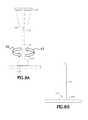
- FIG. 1is a sectional view illustrating a microelectronic package such as fabricated in accordance with an embodiment of the invention.
- FIG. 2is a plan view of the microelectronic package of FIG. 1 .
- FIG. 3Ais a sectional view illustrating an interposer such as fabricated in accordance with an embodiment of the invention.
- FIG. 3Bis a plan view of the interposer of FIG. 3A .
- FIG. 4is a sectional view illustrating a microelectronic assembly such as may incorporate the interposer of FIGS. 3A-3B .
- FIG. 5is a schematic drawing representing movement of a bonding tool in accordance with a method of forming a lead according to an embodiment of the invention.
- FIG. 6illustrates a stage in forming a lead according to an embodiment of the invention.
- FIG. 7illustrates a further stage in forming a lead according to an embodiment of the invention.
- FIG. 8Aillustrates a further stage in forming a lead according to an embodiment of the invention.
- FIG. 8Billustrates a lead formed according to an embodiment of the invention in which the lead has an edge bonded to the metal surface using a stitch bond or wedge bond technique.
- FIG. 9Ais a sectional view illustrating a stage of kinking a wire in a method according to an embodiment of the invention, and illustrating a particular example of a bonding tool.
- FIG. 9Bis a corresponding plan view of the bonding tool shown in FIG. 9A .
- FIG. 9Cis a sectional view illustrating a particular example of a bonding tool.
- FIG. 9Dis a sectional view illustrating a particular example of a bonding tool.
- FIG. 10Ais a side view illustrating a lead formed in accordance with an embodiment of the invention.
- FIG. 10Bis a corresponding plan view of the lead shown in FIG. 10A .
- FIG. 10Cis a side view illustrating a lead formed in accordance with an embodiment of the invention.
- FIG. 10Dis a corresponding plan view of the lead shown in FIG. 10C .
- FIG. 11is a plan view illustrating a stage in a method of forming leads according to an embodiment of the invention.
- FIG. 12is a sectional view corresponding to the plan view of FIG. 11 .
- FIG. 13is a detailed partial sectional view corresponding to FIG. 12 .
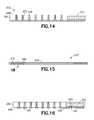
- FIG. 14is a detailed partial sectional view illustrating a stage in a fabrication method subsequent to the stage shown in FIGS. 11 , 12 and 13 in accordance with such embodiment.
- FIG. 15is a sectional view illustrating a stage in a fabrication method subsequent to the stage shown in FIG. 14 .
- FIG. 16is a detailed partial sectional view corresponding to FIG. 15 .
- FIG. 17is a schematic drawing representing movement of a bonding tool in accordance with a method of forming a lead according to an embodiment of the invention.
- FIG. 18illustrates a stage in forming a lead according to an embodiment of the invention.
- FIG. 19illustrates a further stage in forming a lead according to an embodiment of the invention.
- FIG. 20illustrates a further stage in forming a lead according to an embodiment of the invention.
- FIG. 21is a schematic sectional view illustrating a system according to an embodiment of the invention.
- the processes described hereincan be used to form electrically conductive leads 137 which extend from metal pads 110 at a surface 111 of a component to a second surface 144 above the component surface where the leads can be interconnected with corresponding features of a second component, or in some cases, with pads, vias, or traces of a redistribution layer.
- a “lead”refers to an electrically conductive element configured to conduct an electrical current between a contact, e.g., an electrically conductive pad, at a surface of a system or component thereof, e.g., a microelectronic element, a substrate, an interposer, or a circuit panel, among others, to a location at a height above a plane in which the surface lies.
- a contacte.g., an electrically conductive pad
- a surface of a system or component thereofe.g., a microelectronic element, a substrate, an interposer, or a circuit panel, among others.
- An end of the lead remote from the contactmay be exposed for further connection to another component or system.
- the leadmay function as an interconnect, e.g., a via, between the contact and a level of an assembly higher than the contact.
- an electrically conductive elementis “at” a surface of a component indicates that, when the component is not assembled with any other element, the electrically conductive element is available for contact with a theoretical point moving in a direction perpendicular to the surface of the component toward the surface of the component from outside the component.
- a terminal or other conductive element which is at a surface of a substratemay project from such surface; may be flush with such surface; or may be recessed relative to such surface in a hole or depression in the substrate.
- a statement that an element is disposed “above a surface” or “overlying a surface”means at a location which is in an orthogonal direction away from the surface.
- a statement that one element is “above” or “upward from” a reference planemeans at a location in an orthogonal direction away from the reference plane. Movement of an element in an “upward” direction means in a direction to a greater height above a reference plane defined by the surface. Conversely, movement of an element in a “downward” direction means in a direction to a lower height above a reference plane defined by the surface.
- leads 137can be arranged as an array of wire bonds bonded to surfaces of metal pads or other features at the component surface, the leads extending away from the metal pads at least partly in an upward direction.
- Such “bond via array”can provide vertical interconnects for a variety of components and microelectronic assemblies.
- a microelectronic package 10may have a plurality of leads 137 which are available at an upper surface 144 thereof for interconnection with an additional microelectronic package (not shown) disposed above the surface 144 .
- Each of the leads 137has an end 134 bonded to a metal surface of a pad 110 or metal feature at a surface 111 of a dielectric element such as substrate 102 .
- the leads 137can extend in an upwardly direction through a dielectric material such as encapsulation 142 , the leads 137 having ends 138 at a surface 144 of the dielectric element. In the package 10 , portions of edge surfaces 136 of the leads may or may not be uncovered by a dielectric material used to form the encapsulation 142 .
- the package 10can comprise a microelectronic element 121 .
- structure 10can be a microelectronic assembly or package which includes a microelectronic element 121 electrically interconnected with a substrate 102 .
- the microelectronic element 121may be mounted face up to substrate 102 using an adhesive (not shown), with wire bonds 24 or other conductive structure electrically coupling the microelectronic element 121 with the substrate 102 .
- the microelectronic packagecan further include terminals 148 at a lower surface 146 of the package which are available for connection with elements of another component at or below the terminals 148 .
- terminals 148can be bonded to corresponding contacts of a circuit panel or other microelectronic package through conductive masses such as solder balls (not shown), for example.
- the leads 137can provide interconnects for electrically coupling a first set of contacts 348 , e.g., pads, at a first surface 314 of a dielectric element 319 of an interposer 310 with a second set of contacts 358 , e.g., pads, at a second surface 354 of the interposer.
- the dielectric element 319can be formed by molding a dielectric material onto the leads 137 to form an encapsulation.
- An electrically conductive redistribution layercan be provided at one or both of the first and second surfaces 314 , 354 .
- the redistribution layercan comprise contacts 348 , 358 and traces 364 which extend along one or both of the surfaces 314 , 354 and which can be provided for redistributing the contacts and can be provided for electrically coupling one or more of the contacts, or one or more of leads 137 or both.
- FIG. 4depicts an example microelectronic assembly 402 in which interposer 310 can be assembled with microelectronic components 412 , 452 , and may electrically couple the microelectronic elements through elements of a redistribution layer thereon such as traces 364 .
- the interposercan be electrically coupled to a package substrate 425 through elements such as electrically conductive masses, e.g., solder balls attached to contacts 348 at a surface 314 of the interposer 310 .
- the package substrate 425can be electrically coupled to a circuit panel 445 , such as through conductive masses 428 , e.g., solder balls.
- the assemblymay include only one microelectronic element 412 or 452 .
- the package substrate 425may be omitted.
- the circuit panel 445may be electrically coupled to other components in the assembly 402 in ways other than shown in FIG. 4 .
- the bonding toolcan be moved in directions and in a sequential order along segments 120 , 130 , 140 , 150 and 160 of a path such as illustrated in FIG. 5 .
- a bonding tool 104bonds the wire 115 to a metal surface, such as surface 112 of a pad 110 at a surface of a substrate 102 or other component, for example.
- the bonding tool 104can be a capillary type bonding tool in which a wire 115 is fed out through a central opening of the capillary in a direction substantially orthogonal to a surface 122 of the bonding tool.
- a ball bond 114may be formed at an end of the wire that is joined to the metal surface 112 , which may result from applying energy to a portion of the wire exposed beyond surface 122 as the bonding tool surface 122 is moved or positioned adjacent to the metal surface 112 .
- the bonding tooldraws away from the metal surface 112 . Referring to FIG. 6 , since one end of the wire 115 is bonded to the metal surface 112 , the drawing away of the bonding tool causes the wire to extend farther beyond a surface 122 of the bonding tool.
- the bonding toolwhen drawing the bonding tool away from the metal surface, can be moved in an upward direction along path segment 120 away from a reference plane 108 defined by the metal surface 112 .
- movement along path segment 120can be in a direction substantially orthogonal to the surface 111 of the component.
- the bonding toolAfter moving the bonding tool upwardly along path segment 120 , the bonding tool may be moved in a lateral direction along path segment 130 , which may be substantially parallel to the surface 111 .
- the bonding toolmay then be moved upwardly along path segment 140 as shown in FIG. 5 .
- the above-described motion of the bonding toolcan cause a predetermined length of the wire of at least 50 microns to extend between the surface 122 of the bonding tool and the metal surface 112 .
- a “micron”means a millionth of a meter, i.e., a micrometer.
- the shape of the wire 115 and the position of the bonding tool 104 relative to the metal surface 112can be as shown in FIG. 6 .
- a clamp 125can engage the wire 115 to prevent or limit further extension of the wire beyond the surface 122 of the bonding tool.
- the wirecan be clamped at the stage of processing shown in FIG. 6 . The clamping of the wire prevents or limits further extension of the wire in a direction beyond the surface 122 of the bonding tool.
- the bonding tool 104may now be moved along path segment 150 in a different direction than before. This movement of the bonding tool can be used to impart a kink to the wire 115 .
- the bonding toolcan be moved along path segment in a lateral direction other than the lateral direction of travel along the previous path segment 130 .
- Movement along path segment 150may also be in a downward direction towards the reference plane 108 defined by the metal surface 112 .
- the pathmay include any combination of movements in the x-, y-, or z-directions relative to the reference plane.
- the movementsmay be a series of straight lines or one or more curves.
- some or part of the movementsmay comprise motion of the surface 122 of the bonding tool in a loop or motion in a spiral.
- the tool and/or the wiremay be rotated or twisted during the process to further aid in forming the kink or shaping any portion of the wire.
- the bonding toolmay impart a kink 116 to a location of the wire 115 proximate a surface 122 of the tool.
- the kinkmanifests as a locally weakened location of the wire where tension applied to the wire in a longitudinal direction of the wire can cause the wire to break at the weakened location.
- the kinkmay coincide with a local reduction in the diameter or width of the wire in at least one direction.
- contact between wire 115 at an edge of the surface 112 of the bonding toolcan assist in imparting the kink 116 to the wire.
- movement of the bonding toolforms the kink in the wire at a location where the wire is fully separated from any metal element other than that provided on the bonding tool. That is, the kink can be formed without crushing the wire between the bonding tool and another metal element that is stationary or moving separately from the bonding tool. In this way, the kink in the wire can be said to be formed “in air”. In the example shown in FIG.
- the kinkis formed while a lowermost surface 117 of the wire is separated from a surface 111 of the component, e.g., substrate 102 , or other component at a height “h” therefrom.
- the wirealso remains separated from a surface of a ball bond 114 between the wire and the metal surface 112 , that separation distance “s” being depicted in FIG. 7 .
- the wirewhen the wire is joined to the metal surface 112 by a ball bond 114 , and when forming the kink, the wire can be moved to within 100 microns of a surface of the ball bond 114 that bonds the wire 115 to the metal surface 112 , without the wire contacting the ball bond 114 . In a further example, when forming the kink, the wire can be moved to within 20 microns of a surface of the ball bond 114 that bonds the wire 115 to the metal surface 112 , without the wire contacting the ball bond 114 .
- the bonding toolcan be moved in such way that the surface 122 of the bonding tool, or a portion of the wire 115 projecting below that surface 122 , or both the surface 122 and the wire 115 underlying that surface 122 , is at a height from the component surface 111 that is lower than a thickness dimension “t” of a ball bond that joins an end of the wire to the metal surface 112 .
- the bonding toolAfter forming the kink, the bonding tool then is moved in a way that tensions the wire in a longitudinal direction of the wire. Moreover, as seen by arrows 60 , 62 , to further facilitate the severing of the wire, while applying or maintaining the tension on the wire, one or both of the bonding tool or the metal surface, which may be supported on an element 112 , e.g., a component or dielectric element 102 ( FIG. 5 ) can be rotated relative to the other of the metal surface or bonding tool about an axis extending in a direction of a length of the wire. The relative rotational movement between the bonding tool and the metal surface 112 twists the wire, i.e., applies a torsional force thereto.
- an element 112e.g., a component or dielectric element 102 ( FIG. 5 )
- the bonding tool and not the metal surfacemay be rotated relative to the metal surface while the wire is under tension.
- the metal surface and not the bonding toolcan be rotated while the wire is under tension.
- each of the bonding tool and the metal surfacecan be rotated relative to the other of the bonding tool or the metal surface.
- rotationcan be either in a clockwise or counterclockwise direction.
- the relative rotation between the bonding tool and the metal surfacemay be less than one full rotation.
- “one full rotation”means a full rotation of the bonding tool or the metal surface relative to one another about an axis oriented in a direction of the length of the wire.
- the relative rotational motion between the bonding tool and the metal surfacecan be less than one full rotation and may be repeated several times, e.g., up to ten times to sever the wire and form a structure wherein an upwardly projecting end of the wire bond points up as seen in FIG. 8B .
- the bonding toolcan be moved in an upwardly direction relative to the metal surface 112 and relative to the ball bond 114 .
- the clamp 125prevents movement of the wire in the longitudinal direction of the wire. Relative rotational movement between the bonding tool and the metal surface 112 can also twist the wire.
- the wireis weakened at the location of the kink 116 , or the geometry of the wire at the kink concentrates stress at the location of the kink, tensioning and twisting the wire causes the wire to be severed at the location of the kink 116 . As a result, a portion of the wire 115 that forms a lead is severed at the location of the kink 116 from another portion of the wire that extends within the bonding tool 104 .
- the wire 115 processed and severed in this mannermay show signs of the torsional force described herein, such as having a twisted surface about the axis of the wire, or may have a twisted shape, such as a pigtail. This effect may occur along the entire length of the wire 115 or may be restricted only to a portion of the length of the wire or a region, such as near the free end of the wire.
- the leadmay be plated with an electrically conductive barrier material to reduce or avoid diffusion between the metal of which the lead is formed and a bond metal, e.g., solder, or gold which may be used in further bonding the lead to another element or other component.
- a bond metale.g., solder
- the conductive barriercan be palladium.
- the barrier metalcan include one or more of nickel, tungsten, titanium, phosphorus, cobalt, and conductive compounds of the same.
- the wirecan be twisted by relative rotational movement of the bonding tool relative to the metal surface at a time after forming the kink but prior to using the bonding tool to tension the wire.
- twisting of the wirecan begin prior to tensioning the wire, the twisting continuing when the bonding tool applies the tension to the wire.
- the lead shown in FIG. 8Bcan be formed with a different type of bond between the wire 115 and the metal surface 112 .
- the wirecan be bonded to the metal surface with a stitch bond or wedge bond in which an edge 127 of the wire 115 is bonded to the metal surface 112 and the wire 115 bends upwardly away from the metal surface 112 .
- the bonded end 134 of the lead seen in FIG. 1is the portion of the wire that is stitch-bonded to the metal surface.
- the formation of the stitch bond or wedge bond between the wire and the metal surface 112can be as further described in U.S. application Ser. No.
- the bonding toolcan be a wedge-bonding tool rather than a capillary type tool, which can be used to form a wedge bond between the wire and the metal surface.
- FIGS. 9A-Bdepict a particular bonding tool arrangement which can be used in accordance with the above-described method of forming a lead.
- the bonding tool 104can include a forming element 334 at an exterior surface 332 of the bonding tool 104 .
- the forming element 334can be provided at an exterior generally cylindrical or frustoconical wall surface 332 of the bonding tool which surrounds the central opening 124 of the bonding tool through which the wire extends.
- the forming elementcan be disposed at some distance from an entrance 323 of the central opening 124 .
- the forming elementcan assist in imparting the kink. Movement of the bonding tool forces the wire against the forming element 334 .
- the forming element 334can include an edge 338 against which the wire is forced during the movement of the bonding tool.
- the edge 338 of the forming elementexists at a junction of two surfaces which meet with an angle 340 of less than 180 degrees passing through an interior of the forming element.
- the edge 342can be a “knife edge”, i.e., an edge at the junction of two surfaces which meet an interior angle 344 measuring less than 90 degrees.
- the interior angle 344 of the two surfaces which form the edge 342will be smaller.
- the angle 344may be beneficial to limit the angle 344 to 75 degrees or less, and in other cases, it may be beneficial to limit the angle 344 to 60 degrees or less.
- the edge 342is “sharp”, i.e., having a relatively small interior angle between the surfaces of typically less than 75 degrees, the edge 342 may be forced more deeply into the wire 115 during the movement of the bonding tool.
- the height 339 of the edge 338 above an adjacent outer surface of the 332 of the bonding toolcan be limited such that the edge 338 extends into the interior of the wire 115 but without severing the wire during the movement depicted in FIG. 9A .
- the edge 338can be located at an axial distance 336 along the exterior surface 332 which is at least 0.25 times a diameter of the wire 115 used to form the lead.
- the edgecan be located at a height 339 above an adjacent outer surface 332 of the bonding tool which is at least 0.25 times a diameter of the wire 115 used to form the lead.
- the forming element 334can be applied to the exterior surface 332 of a bonding tool to thereby form a part of the bonding tool 104 as used in practicing a method as described herein.
- a forming element 334 having an annular shapecan be provided at an exterior surface 332 of the bonding tool, and can be attached or fitted thereon.
- the forming elementcan be a “blade skirt” which is fitted onto the exterior surface 332 .
- the forming elementmay be an integrally formed portion of the exterior surface 332 .
- the edge 338 of the forming elementmay be oriented in a downward direction towards the metal surface from the bonding tool.
- ends of the leads formed in this mannercan have shapes such as those shown in FIGS. 10A-B .
- the diameter 119 of a lead at an end 135 of the lead remote from the metal surfacecan be reduced relative to a normal diameter of the lead at other locations along the wire.
- the normal diameter of the leadcan be the same as, or essentially the same as a normal diameter 118 of the wire which exists at almost all places along the length of the wire except for a location at which the wire is bonded to another element such as metal surface, and except for the end 135 of the lead.
- FIGS. 10A-Bends of the leads formed in this manner can have shapes such as those shown in FIGS. 10A-B .
- the diameter 119 of a lead at an end 135 of the lead remote from the metal surfacecan be reduced relative to a normal diameter of the lead at other locations along the wire.
- the normal diameter of the leadcan be the same as, or essentially the same as a normal diameter 118 of the wire which exists at almost all places along the length of
- the formed leadhas a width 219 that is reduced in one direction relative to a normal diameter 218 of the lead which can be the same as a normal diameter of the wire, as described above.
- the width 221 of the lead in a second directionmay be the same as, or greater than the normal diameter 218 of the lead at locations between the end 235 and the metal surface 112 .
- the above described processingmay then be repeated to form a plurality of leads 137 each having an end bonded to a metal surface of a metal feature at a surface of a dielectric structure of the component.
- the processcan be repeated to form a plurality of leads 137 having bases 134 bonded to respective metal surfaces 112 (electrically conductive pads) at a surface 111 of a dielectric element 102 , e.g., a substrate.
- a dielectric element 142can be formed which surrounds individual leads 137 of the plurality of leads, wherein the ends 138 of the leads are uncovered by the dielectric element 142 at a surface 144 of the dielectric element.
- the dielectric element 144can be formed by molding an encapsulant surrounding the individual leads 137 of the plurality of leads. In the structure 10 , portions of edge surfaces 136 of the leads may or may not be uncovered by a dielectric material used to form the encapsulation.
- a plurality of leadsmay be formed on a common metal surface such as shown in FIGS. 11 , 12 and 13 .
- microelectronic element 222can be mounted to a metal sheet 220 and wires bonded to the metal sheet and formed into leads 237 in an assembly 210 in accordance with the above-described processing.
- a dielectric element 242e.g., an encapsulation, can be formed surrounding individual leads 237 of the plurality of leads of assembly 210 , with ends 238 of the leads being uncovered by the dielectric element 242 at a surface 244 of the dielectric element 242 . Referring to FIG.
- the metal elemente.g., a metal sheet 220
- the metal elementcan be patterned to form a plurality of metal features 228 at a lower surface 245 of the dielectric element 242 .
- the metal featurescan include traces 229 , vias 231 , etc. which electrically couple pads 228 at a surface 245 of the dielectric element, e.g., encapsulation, with contacts 224 at a surface of the microelectronic element 222 .
- the bonding toolneed not be moved in a manner as seen in FIG. 5 along substantially vertical path segments 120 , 140 and a horizontal path segment 130 . Instead, with the wire bonded to the metal surface 112 , the bonding tool can be drawn away from the metal surface 112 along a path segment 230 which is at an angle relative to both the vertical direction 290 and at an angle to the horizontal direction 295 . After moving the bonding tool along the path segment 230 , the wire then can be clamped to prevent or limit further extension of the wire beyond the surface 122 of the bonding tool.
- the bonding toolcan be moved in a direction that is both lateral relative to the surface 111 of the component and downward along path segment 240 .
- FIG. 18further depicts the shape of the wire 115 after the bonding tool 104 has been moved along path segment 230 , after clamping the wire, and after the bonding tool has begun moving in the lateral and downward direction along path segment 240 .
- FIG. 19depicts the shape of the wire 115 after the bonding tool has been moved along path segments 230 , 240 to a location at which a kink is applied to the wire, such as described in the foregoing. Referring to FIG. 20 , further movement of the wire which causes the wire to be severed at the location of the kink can be the same that described above with reference to FIG. 8A .
- microelectronic packages and microelectronic assemblies described above with reference to FIGS. 1 through 4 and FIG. 16can be utilized in construction of diverse electronic systems, such as the system 1100 shown in FIG. 21 .
- the system 1100 in accordance with a further embodiment of the inventionincludes a plurality of modules or components 1106 such as the microelectronic packages and/or microelectronic assemblies as described above in conjunction with other electronic components 1108 and 1110 .
- the systemcan include a circuit panel, motherboard, or riser panel 1102 such as a flexible printed circuit board, and the circuit panel can include numerous conductors 1104 , of which only one is depicted in FIG. 21 , interconnecting the modules or components 1106 with one another.
- a circuit panel 1102can transport signals to and from each of the microelectronic packages and/or microelectronic assemblies included in the system 1100 .
- thisis merely exemplary; any suitable structure for making electrical connections between the modules or components 1106 can be used.
- the system 1100can also include a processor such as the semiconductor chip 1108 , such that each module or component 1106 can be configured to transfer a number N of data bits in parallel in a clock cycle, and the processor can be configured to transfer a number M of data bits in parallel in a clock cycle, M being greater than or equal to N.
- component 1108can be a semiconductor chip and component 1110 is a display screen, but any other components can be used in the system 1100 .
- the system 1100can include any number of such components.
- Modules or components 1106 and components 1108 and 1110can be mounted in a common housing 1101 , schematically depicted in broken lines, and can be electrically interconnected with one another as necessary to form the desired circuit.
- the housing 1101is depicted as a portable housing of the type usable, for example, in a smartphone, tablet computer, or cellular telephone, and screen 1110 can be exposed at the surface of the housing.
- a structure 1106includes a light-sensitive element such as an imaging chip
- a lens 1111 or other optical devicealso can be provided for routing light to the structure.
- the simplified system shown in FIG. 21is merely exemplary; other systems, including systems commonly regarded as fixed structures, such as desktop computers, routers and the like can be made using the structures discussed above.
Landscapes
- Engineering & Computer Science (AREA)
- Power Engineering (AREA)
- Microelectronics & Electronic Packaging (AREA)
- Computer Hardware Design (AREA)
- Manufacturing & Machinery (AREA)
- Condensed Matter Physics & Semiconductors (AREA)
- General Physics & Mathematics (AREA)
- Physics & Mathematics (AREA)
- Mechanical Engineering (AREA)
- Ceramic Engineering (AREA)
- Wire Bonding (AREA)
- Manufacturing Of Electrical Connectors (AREA)
- Encapsulation Of And Coatings For Semiconductor Or Solid State Devices (AREA)
Abstract
Description
- This application is a continuation-in-part of U.S. application Ser. No. 14/077,597 filed Nov. 12, 2013, the disclosure of which is incorporated by reference herein.
- 1. Field of the Invention
- The subject matter of the present application relates to fabrication of microelectronic components, packages, and assemblies, such items having bond wires which function as interconnects extending at least partially in a generally vertically direction.
- 2. Description of the Related Art
- Microelectronic devices such as semiconductor chips typically require many input and output connections to other electronic components. The input and output contacts of a semiconductor chip or other comparable device are generally disposed in grid-like patterns that substantially cover a surface of the device (commonly referred to as an “area array”) or in elongated rows which may extend parallel to and adjacent each edge of the device's front surface, or in the center of the front surface. Typically, devices such as chips must be physically mounted on a substrate such as a printed circuit board, and the contacts of the device must be electrically connected to electrically conductive features of the circuit board.
- Semiconductor chips are commonly provided in packages that facilitate handling of the chip during manufacture and during mounting of the chip on an external substrate such as a circuit board or other circuit panel. For example, many semiconductor chips are provided in packages suitable for surface mounting. Numerous packages of this general type have been proposed for various applications. Most commonly, such packages include a dielectric element, commonly referred to as a “chip carrier” with terminals formed as plated or etched metallic structures on the dielectric. These terminals typically are connected to the contacts of the chip itself by features such as thin traces extending along the chip carrier itself and by fine leads or wires extending between the contacts of the chip and the terminals or traces. In a surface mounting operation, the package is placed onto a circuit board so that each terminal on the package is aligned with a corresponding contact pad on the circuit board. Solder or other bonding material is provided between the terminals and the contact pads. The package can be permanently bonded in place by heating the assembly so as to melt or “reflow” the solder or otherwise activate the bonding material.
- Many packages include solder masses in the form of solder balls, typically about 0.1 mm and about 0.8 mm (5 and 30 mils) in diameter, attached to the terminals of the package. A package having an array of solder balls projecting from its bottom surface is commonly referred to as a ball grid array or “BGA” package. Other packages, referred to as land grid array or “LGA” packages are secured to the substrate by thin layers or lands formed from solder. Packages of this type can be quite compact. Certain packages, commonly referred to as “chip scale packages,” occupy an area of the circuit board equal to, or only slightly larger than, the area of the device incorporated in the package. This is advantageous in that it reduces the overall size of the assembly and permits the use of short interconnections between various devices on the substrate, which in turn limits signal propagation time between devices and thus facilitates operation of the assembly at high speeds.
- Packaged semiconductor chips are often provided in “stacked” arrangements, wherein one package is provided, for example, on a circuit board, and another package is mounted on top of the first package. These arrangements can allow a number of different chips to be mounted within a single footprint on a circuit board and can further facilitate high-speed operation by providing a short interconnection between packages. Often, this interconnect distance is only slightly larger than the thickness of the chip itself. For interconnection to be achieved within a stack of chip packages, it is necessary to provide structures for mechanical and electrical connection on both sides of each package (except for the topmost package). This has been done, for example, by providing contact pads or lands on both sides of the substrate to which the chip is mounted, the pads being connected through the substrate by conductive vias or the like. Solder balls or the like have been used to bridge the gap between the contacts on the top of a lower substrate to the contacts on the bottom of the next higher substrate. The solder balls must be higher than the height of the chip in order to connect the contacts. Examples of stacked chip arrangements and interconnect structures are provided in U.S. Patent App. Pub. No. 2010/0232129 (“the '129 Publication”), the disclosure of which is incorporated by reference herein in its entirety.
- Microcontact elements in the form of elongated posts or pins may be used to connect microelectronic packages to circuit boards and for other connections in microelectronic packaging. In some instances, microcontacts have been formed by etching a metallic structure including one or more metallic layers to form the microcontacts. The etching process limits the size of the microcontacts. Conventional etching processes typically cannot form microcontacts with a large ratio of height to maximum width, referred to herein as “aspect ratio”. It has been difficult or impossible to form arrays of microcontacts with appreciable height and very small pitch or spacing between adjacent microcontacts. Moreover, the configurations of the microcontacts formed by conventional etching processes are limited.
- Despite all of the above-described advances in the art, still further improvements in making and testing microelectronic packages would be desirable.
- An electrically conductive lead can be formed using a bonding tool. In one embodiment, after bonding the wire to a metal surface and extending a length of the wire beyond the bonding tool, the wire is clamped. Movement of the bonding tool can impart a kink to the wire at a location where the wire is fully separated from any metal element other than the bonding tool. A forming element, e.g., an edge or a blade skirt provided at an exterior surface of the bonding tool can help kink the wire. Tensioning the wire using the bonding tool and twisting the wire, causes the wire to break and define an end. The lead then extends from the metal surface to the end.
- In one example, twisting of the wire comprises imparting relative rotational motion between the bonding tool and the metal surface about an axis in a direction of a length of the wire. In one example, the relative rotational motion may be less than or equal to one full rotation, wherein one full rotation means a full rotation of the bonding tool or the metal surface relative to one another about an axis oriented in a direction of a length of the wire. In one particular example, the relative rotational motion may be repeated a number of times, e.g., ten times in order to sever the wire.
- In a method according to one example, an electrically conductive lead of a component can be formed by steps comprising: using a bonding tool to bond a wire extending beyond a surface of a bonding tool to a metal surface; drawing the bonding tool away from the metal surface while allowing the wire to extend farther from the surface of the bonding tool; clamping the wire to limit further extension of the wire beyond the surface of the bonding tool; moving the bonding tool while the wire remains clamped such that the bonding tool imparts a kink to the wire at a location where the wire is fully separated from any metal element other than the bonding tool; and twisting the wire and tensioning the wire using the bonding tool such that the wire breaks at the kink to define an end, wherein the lead comprises the wire extending from the metal surface to the end.
- The wire processed and severed in this manner may show signs of the torsional force described herein, such as having a twisted surface about the axis of the wire, or may have a twisted shape, such as a pigtail. This effect may occur along the entire length of the wire or may be restricted only to a portion of the length of the wire or a region, such as near the free end of the wire.
- Various components can incorporate the leads formed in accordance with the embodiments of the method provided herein.
- Various movements of the bonding tool and shapes of conductive leads can be achieved in accordance with the embodiments of the method provided herein.
FIG. 1 is a sectional view illustrating a microelectronic package such as fabricated in accordance with an embodiment of the invention.FIG. 2 is a plan view of the microelectronic package ofFIG. 1 .FIG. 3A is a sectional view illustrating an interposer such as fabricated in accordance with an embodiment of the invention.FIG. 3B is a plan view of the interposer ofFIG. 3A .FIG. 4 is a sectional view illustrating a microelectronic assembly such as may incorporate the interposer ofFIGS. 3A-3B .FIG. 5 is a schematic drawing representing movement of a bonding tool in accordance with a method of forming a lead according to an embodiment of the invention.FIG. 6 illustrates a stage in forming a lead according to an embodiment of the invention.FIG. 7 illustrates a further stage in forming a lead according to an embodiment of the invention.FIG. 8A illustrates a further stage in forming a lead according to an embodiment of the invention.FIG. 8B illustrates a lead formed according to an embodiment of the invention in which the lead has an edge bonded to the metal surface using a stitch bond or wedge bond technique.FIG. 9A is a sectional view illustrating a stage of kinking a wire in a method according to an embodiment of the invention, and illustrating a particular example of a bonding tool.FIG. 9B is a corresponding plan view of the bonding tool shown inFIG. 9A .FIG. 9C is a sectional view illustrating a particular example of a bonding tool.FIG. 9D is a sectional view illustrating a particular example of a bonding tool.FIG. 10A is a side view illustrating a lead formed in accordance with an embodiment of the invention.FIG. 10B is a corresponding plan view of the lead shown inFIG. 10A .FIG. 10C is a side view illustrating a lead formed in accordance with an embodiment of the invention.FIG. 10D is a corresponding plan view of the lead shown inFIG. 10C .FIG. 11 is a plan view illustrating a stage in a method of forming leads according to an embodiment of the invention.FIG. 12 is a sectional view corresponding to the plan view ofFIG. 11 .FIG. 13 is a detailed partial sectional view corresponding toFIG. 12 .FIG. 14 is a detailed partial sectional view illustrating a stage in a fabrication method subsequent to the stage shown inFIGS. 11 ,12 and13 in accordance with such embodiment.FIG. 15 is a sectional view illustrating a stage in a fabrication method subsequent to the stage shown inFIG. 14 .FIG. 16 is a detailed partial sectional view corresponding toFIG. 15 .FIG. 17 is a schematic drawing representing movement of a bonding tool in accordance with a method of forming a lead according to an embodiment of the invention.FIG. 18 illustrates a stage in forming a lead according to an embodiment of the invention.FIG. 19 illustrates a further stage in forming a lead according to an embodiment of the invention.FIG. 20 illustrates a further stage in forming a lead according to an embodiment of the invention.FIG. 21 is a schematic sectional view illustrating a system according to an embodiment of the invention.- Referring to
FIG. 1 , the processes described herein can be used to form electricallyconductive leads 137 which extend frommetal pads 110 at asurface 111 of a component to asecond surface 144 above the component surface where the leads can be interconnected with corresponding features of a second component, or in some cases, with pads, vias, or traces of a redistribution layer. A “lead” refers to an electrically conductive element configured to conduct an electrical current between a contact, e.g., an electrically conductive pad, at a surface of a system or component thereof, e.g., a microelectronic element, a substrate, an interposer, or a circuit panel, among others, to a location at a height above a plane in which the surface lies. An end of the lead remote from the contact may be exposed for further connection to another component or system. Alternatively, the lead may function as an interconnect, e.g., a via, between the contact and a level of an assembly higher than the contact. - As used in this disclosure with reference to a component, e.g., an interposer, microelectronic element, circuit panel, substrate, etc., a statement that an electrically conductive element is “at” a surface of a component indicates that, when the component is not assembled with any other element, the electrically conductive element is available for contact with a theoretical point moving in a direction perpendicular to the surface of the component toward the surface of the component from outside the component. Thus, a terminal or other conductive element which is at a surface of a substrate may project from such surface; may be flush with such surface; or may be recessed relative to such surface in a hole or depression in the substrate.
- As used herein, a statement that an element is disposed “above a surface” or “overlying a surface” means at a location which is in an orthogonal direction away from the surface. A statement that one element is “above” or “upward from” a reference plane means at a location in an orthogonal direction away from the reference plane. Movement of an element in an “upward” direction means in a direction to a greater height above a reference plane defined by the surface. Conversely, movement of an element in a “downward” direction means in a direction to a lower height above a reference plane defined by the surface. All such statements and meanings of the foregoing terms are not in a gravitational reference, but rather in the frame of reference defined by the element itself.
- As seen in
FIGS. 1-2 , leads137 can be arranged as an array of wire bonds bonded to surfaces of metal pads or other features at the component surface, the leads extending away from the metal pads at least partly in an upward direction. Such “bond via array” can provide vertical interconnects for a variety of components and microelectronic assemblies. For example, amicroelectronic package 10 may have a plurality ofleads 137 which are available at anupper surface 144 thereof for interconnection with an additional microelectronic package (not shown) disposed above thesurface 144. Each of theleads 137 has anend 134 bonded to a metal surface of apad 110 or metal feature at asurface 111 of a dielectric element such assubstrate 102. The leads137 can extend in an upwardly direction through a dielectric material such asencapsulation 142, theleads 137 havingends 138 at asurface 144 of the dielectric element. In thepackage 10, portions of edge surfaces136 of the leads may or may not be uncovered by a dielectric material used to form theencapsulation 142. - As further seen in
FIG. 1 , thepackage 10 can comprise amicroelectronic element 121. Specifically,structure 10 can be a microelectronic assembly or package which includes amicroelectronic element 121 electrically interconnected with asubstrate 102. Themicroelectronic element 121 may be mounted face up tosubstrate 102 using an adhesive (not shown), withwire bonds 24 or other conductive structure electrically coupling themicroelectronic element 121 with thesubstrate 102. The microelectronic package can further include terminals148 at alower surface 146 of the package which are available for connection with elements of another component at or below the terminals148. For example, terminals148 can be bonded to corresponding contacts of a circuit panel or other microelectronic package through conductive masses such as solder balls (not shown), for example. - In another example, as seen in
FIGS. 3A-B , theleads 137 can provide interconnects for electrically coupling a first set ofcontacts 348, e.g., pads, at afirst surface 314 of adielectric element 319 of aninterposer 310 with a second set ofcontacts 358, e.g., pads, at asecond surface 354 of the interposer. Thedielectric element 319 can be formed by molding a dielectric material onto theleads 137 to form an encapsulation. An electrically conductive redistribution layer can be provided at one or both of the first andsecond surfaces contacts surfaces leads 137 or both. FIG. 4 depicts an examplemicroelectronic assembly 402 in which interposer310 can be assembled withmicroelectronic components package substrate 425 through elements such as electrically conductive masses, e.g., solder balls attached tocontacts 348 at asurface 314 of theinterposer 310. In turn, thepackage substrate 425 can be electrically coupled to acircuit panel 445, such as throughconductive masses 428, e.g., solder balls.- In other variations, one or more of the components seen in
FIG. 4 may not be present. For example, the assembly may include only onemicroelectronic element package substrate 425 may be omitted. In one example, thecircuit panel 445 may be electrically coupled to other components in theassembly 402 in ways other than shown inFIG. 4 . - Turning now to
FIGS. 5 through 8A , a method will be described for forming an electrically conductive lead of a component such as any of the components described above. In this embodiment, the bonding tool can be moved in directions and in a sequential order alongsegments FIG. 5 . Referring toFIG. 6 , in a first stage of forming the lead, abonding tool 104 bonds thewire 115 to a metal surface, such assurface 112 of apad 110 at a surface of asubstrate 102 or other component, for example. In one example, thebonding tool 104 can be a capillary type bonding tool in which awire 115 is fed out through a central opening of the capillary in a direction substantially orthogonal to asurface 122 of the bonding tool. - When bonding the wire, a
ball bond 114 may be formed at an end of the wire that is joined to themetal surface 112, which may result from applying energy to a portion of the wire exposed beyondsurface 122 as thebonding tool surface 122 is moved or positioned adjacent to themetal surface 112. After applying energy to form the bond to themetal surface 112, the bonding tool draws away from themetal surface 112. Referring toFIG. 6 , since one end of thewire 115 is bonded to themetal surface 112, the drawing away of the bonding tool causes the wire to extend farther beyond asurface 122 of the bonding tool. Also, when drawing the bonding tool away from the metal surface, the bonding tool can be moved in an upward direction alongpath segment 120 away from areference plane 108 defined by themetal surface 112. In one example, movement alongpath segment 120 can be in a direction substantially orthogonal to thesurface 111 of the component. After moving the bonding tool upwardly alongpath segment 120, the bonding tool may be moved in a lateral direction alongpath segment 130, which may be substantially parallel to thesurface 111. The bonding tool may then be moved upwardly alongpath segment 140 as shown inFIG. 5 . The above-described motion of the bonding tool can cause a predetermined length of the wire of at least 50 microns to extend between thesurface 122 of the bonding tool and themetal surface 112. As commonly understood, as used herein a “micron” means a millionth of a meter, i.e., a micrometer. - At this stage, the shape of the
wire 115 and the position of thebonding tool 104 relative to themetal surface 112 can be as shown inFIG. 6 . As depicted inFIG. 6 , aclamp 125 can engage thewire 115 to prevent or limit further extension of the wire beyond thesurface 122 of the bonding tool. In one example, the wire can be clamped at the stage of processing shown inFIG. 6 . The clamping of the wire prevents or limits further extension of the wire in a direction beyond thesurface 122 of the bonding tool. - Referring again to
FIG. 5 , after clamping thewire 115, thebonding tool 104 may now be moved alongpath segment 150 in a different direction than before. This movement of the bonding tool can be used to impart a kink to thewire 115. - In one example, the bonding tool can be moved along path segment in a lateral direction other than the lateral direction of travel along the
previous path segment 130. Movement alongpath segment 150 may also be in a downward direction towards thereference plane 108 defined by themetal surface 112. The path may include any combination of movements in the x-, y-, or z-directions relative to the reference plane. The movements may be a series of straight lines or one or more curves. In examples, some or part of the movements may comprise motion of thesurface 122 of the bonding tool in a loop or motion in a spiral. Moreover, the tool and/or the wire may be rotated or twisted during the process to further aid in forming the kink or shaping any portion of the wire. - In one example, the bonding tool may impart a
kink 116 to a location of thewire 115 proximate asurface 122 of the tool. As further explained below, the kink manifests as a locally weakened location of the wire where tension applied to the wire in a longitudinal direction of the wire can cause the wire to break at the weakened location. The kink may coincide with a local reduction in the diameter or width of the wire in at least one direction. - As seen in
FIG. 7 , contact betweenwire 115 at an edge of thesurface 112 of the bonding tool can assist in imparting thekink 116 to the wire. As also seen inFIG. 7 , movement of the bonding tool forms the kink in the wire at a location where the wire is fully separated from any metal element other than that provided on the bonding tool. That is, the kink can be formed without crushing the wire between the bonding tool and another metal element that is stationary or moving separately from the bonding tool. In this way, the kink in the wire can be said to be formed “in air”. In the example shown inFIG. 7 , the kink is formed while alowermost surface 117 of the wire is separated from asurface 111 of the component, e.g.,substrate 102, or other component at a height “h” therefrom. During movement of the wire which imparts the kink, the wire also remains separated from a surface of aball bond 114 between the wire and themetal surface 112, that separation distance “s” being depicted inFIG. 7 . - In a particular example, when the wire is joined to the
metal surface 112 by aball bond 114, and when forming the kink, the wire can be moved to within 100 microns of a surface of theball bond 114 that bonds thewire 115 to themetal surface 112, without the wire contacting theball bond 114. In a further example, when forming the kink, the wire can be moved to within 20 microns of a surface of theball bond 114 that bonds thewire 115 to themetal surface 112, without the wire contacting theball bond 114. - In a particular example, the bonding tool can be moved in such way that the
surface 122 of the bonding tool, or a portion of thewire 115 projecting below thatsurface 122, or both thesurface 122 and thewire 115 underlying thatsurface 122, is at a height from thecomponent surface 111 that is lower than a thickness dimension “t” of a ball bond that joins an end of the wire to themetal surface 112. - After forming the kink, the bonding tool then is moved in a way that tensions the wire in a longitudinal direction of the wire. Moreover, as seen by
arrows element 112, e.g., a component or dielectric element102 (FIG. 5 ) can be rotated relative to the other of the metal surface or bonding tool about an axis extending in a direction of a length of the wire. The relative rotational movement between the bonding tool and themetal surface 112 twists the wire, i.e., applies a torsional force thereto. In one example, the bonding tool and not the metal surface may be rotated relative to the metal surface while the wire is under tension. In another example, the metal surface and not the bonding tool can be rotated while the wire is under tension. In still another example, each of the bonding tool and the metal surface can be rotated relative to the other of the bonding tool or the metal surface. As implied byarrows FIG. 8B . In a specific example of operation, as seen inFIG. 8A , the bonding tool can be moved in an upwardly direction relative to themetal surface 112 and relative to theball bond 114. Theclamp 125 prevents movement of the wire in the longitudinal direction of the wire. Relative rotational movement between the bonding tool and themetal surface 112 can also twist the wire. Because the wire is weakened at the location of thekink 116, or the geometry of the wire at the kink concentrates stress at the location of the kink, tensioning and twisting the wire causes the wire to be severed at the location of thekink 116. As a result, a portion of thewire 115 that forms a lead is severed at the location of thekink 116 from another portion of the wire that extends within thebonding tool 104. - The
wire 115 processed and severed in this manner may show signs of the torsional force described herein, such as having a twisted surface about the axis of the wire, or may have a twisted shape, such as a pigtail. This effect may occur along the entire length of thewire 115 or may be restricted only to a portion of the length of the wire or a region, such as near the free end of the wire. - After forming the lead, the lead may be plated with an electrically conductive barrier material to reduce or avoid diffusion between the metal of which the lead is formed and a bond metal, e.g., solder, or gold which may be used in further bonding the lead to another element or other component. In one example, the conductive barrier can be palladium. In other examples, without limitation, the barrier metal can include one or more of nickel, tungsten, titanium, phosphorus, cobalt, and conductive compounds of the same.
- In a variation of the above-described embodiment, the wire can be twisted by relative rotational movement of the bonding tool relative to the metal surface at a time after forming the kink but prior to using the bonding tool to tension the wire. In another variation, twisting of the wire can begin prior to tensioning the wire, the twisting continuing when the bonding tool applies the tension to the wire.
- Referring to
FIG. 8B , in a variation of the method shown and described relative toFIGS. 5 through 8A , the lead shown inFIG. 8B can be formed with a different type of bond between thewire 115 and themetal surface 112. In this case, the wire can be bonded to the metal surface with a stitch bond or wedge bond in which an edge127 of thewire 115 is bonded to themetal surface 112 and thewire 115 bends upwardly away from themetal surface 112. In this case, the bondedend 134 of the lead seen inFIG. 1 is the portion of the wire that is stitch-bonded to the metal surface. The formation of the stitch bond or wedge bond between the wire and themetal surface 112 can be as further described in U.S. application Ser. No. 13/404,408 filed Feb. 24, 2012, the disclosure of which is incorporated by reference herein. In still another example, the bonding tool can be a wedge-bonding tool rather than a capillary type tool, which can be used to form a wedge bond between the wire and the metal surface. FIGS. 9A-B depict a particular bonding tool arrangement which can be used in accordance with the above-described method of forming a lead. In this example, thebonding tool 104 can include a formingelement 334 at anexterior surface 332 of thebonding tool 104. In the example shown inFIG. 9A , the formingelement 334 can be provided at an exterior generally cylindrical orfrustoconical wall surface 332 of the bonding tool which surrounds thecentral opening 124 of the bonding tool through which the wire extends. In this case, the forming element can be disposed at some distance from anentrance 323 of thecentral opening 124. When the bonding tool is moved after the wire is clamped per the description provided above relative toFIGS. 5 through 7 , the forming element can assist in imparting the kink. Movement of the bonding tool forces the wire against the formingelement 334.- In a particular embodiment, the forming
element 334 can include anedge 338 against which the wire is forced during the movement of the bonding tool. As seen inFIG. 9C , for example, theedge 338 of the forming element exists at a junction of two surfaces which meet with anangle 340 of less than 180 degrees passing through an interior of the forming element. In one example, theedge 342 can be a “knife edge”, i.e., an edge at the junction of two surfaces which meet aninterior angle 344 measuring less than 90 degrees. In a further example, theinterior angle 344 of the two surfaces which form theedge 342 will be smaller. In some cases, it may be beneficial to limit theangle 344 to 75 degrees or less, and in other cases, it may be beneficial to limit theangle 344 to 60 degrees or less. When theedge 342 is “sharp”, i.e., having a relatively small interior angle between the surfaces of typically less than 75 degrees, theedge 342 may be forced more deeply into thewire 115 during the movement of the bonding tool. However, in such case, theheight 339 of theedge 338 above an adjacent outer surface of the332 of the bonding tool can be limited such that theedge 338 extends into the interior of thewire 115 but without severing the wire during the movement depicted inFIG. 9A . In a particular example, theedge 338 can be located at anaxial distance 336 along theexterior surface 332 which is at least 0.25 times a diameter of thewire 115 used to form the lead. In the same example, or in other examples herein, the edge can be located at aheight 339 above an adjacentouter surface 332 of the bonding tool which is at least 0.25 times a diameter of thewire 115 used to form the lead. - The forming
element 334 can be applied to theexterior surface 332 of a bonding tool to thereby form a part of thebonding tool 104 as used in practicing a method as described herein. For example, a formingelement 334 having an annular shape can be provided at anexterior surface 332 of the bonding tool, and can be attached or fitted thereon. In one example, the forming element can be a “blade skirt” which is fitted onto theexterior surface 332. In another example, the forming element may be an integrally formed portion of theexterior surface 332. In still another example, theedge 338 of the forming element may be oriented in a downward direction towards the metal surface from the bonding tool. - In particular examples, ends of the leads formed in this manner can have shapes such as those shown in
FIGS. 10A-B . In the example seen inFIGS. 10A-B , thediameter 119 of a lead at anend 135 of the lead remote from the metal surface can be reduced relative to a normal diameter of the lead at other locations along the wire. In this case, the normal diameter of the lead can be the same as, or essentially the same as anormal diameter 118 of the wire which exists at almost all places along the length of the wire except for a location at which the wire is bonded to another element such as metal surface, and except for theend 135 of the lead. In another example, as seen inFIGS. 10C-D , the formed lead has awidth 219 that is reduced in one direction relative to anormal diameter 218 of the lead which can be the same as a normal diameter of the wire, as described above. In such case, thewidth 221 of the lead in a second direction may be the same as, or greater than thenormal diameter 218 of the lead at locations between theend 235 and themetal surface 112. - Referring again to
FIG. 1 , the above described processing may then be repeated to form a plurality ofleads 137 each having an end bonded to a metal surface of a metal feature at a surface of a dielectric structure of the component. For example, the process can be repeated to form a plurality ofleads 137 havingbases 134 bonded to respective metal surfaces112 (electrically conductive pads) at asurface 111 of adielectric element 102, e.g., a substrate. In a further stage of processing, adielectric element 142 can be formed which surrounds individual leads137 of the plurality of leads, wherein theends 138 of the leads are uncovered by thedielectric element 142 at asurface 144 of the dielectric element. In one example, thedielectric element 144 can be formed by molding an encapsulant surrounding the individual leads137 of the plurality of leads. In thestructure 10, portions of edge surfaces136 of the leads may or may not be uncovered by a dielectric material used to form the encapsulation. - In another example, a plurality of leads may be formed on a common metal surface such as shown in
FIGS. 11 ,12 and13. In this example,microelectronic element 222 can be mounted to ametal sheet 220 and wires bonded to the metal sheet and formed intoleads 237 in anassembly 210 in accordance with the above-described processing. Referring toFIGS. 14-15 , adielectric element 242, e.g., an encapsulation, can be formed surrounding individual leads237 of the plurality of leads ofassembly 210, withends 238 of the leads being uncovered by thedielectric element 242 at asurface 244 of thedielectric element 242. Referring toFIG. 16 , in subsequent processing, the metal element, e.g., ametal sheet 220, can be patterned to form a plurality of metal features228 at alower surface 245 of thedielectric element 242. The metal features can includetraces 229, vias231, etc. which electricallycouple pads 228 at asurface 245 of the dielectric element, e.g., encapsulation, withcontacts 224 at a surface of themicroelectronic element 222. - Referring to
FIGS. 17 through 20 , in a variation of the above-described process of forming a lead, the bonding tool need not be moved in a manner as seen inFIG. 5 along substantiallyvertical path segments horizontal path segment 130. Instead, with the wire bonded to themetal surface 112, the bonding tool can be drawn away from themetal surface 112 along apath segment 230 which is at an angle relative to both thevertical direction 290 and at an angle to thehorizontal direction 295. After moving the bonding tool along thepath segment 230, the wire then can be clamped to prevent or limit further extension of the wire beyond thesurface 122 of the bonding tool. - Thereafter, as further shown in
FIGS. 17-18 , the bonding tool can be moved in a direction that is both lateral relative to thesurface 111 of the component and downward alongpath segment 240.FIG. 18 further depicts the shape of thewire 115 after thebonding tool 104 has been moved alongpath segment 230, after clamping the wire, and after the bonding tool has begun moving in the lateral and downward direction alongpath segment 240.FIG. 19 depicts the shape of thewire 115 after the bonding tool has been moved alongpath segments FIG. 20 , further movement of the wire which causes the wire to be severed at the location of the kink can be the same that described above with reference toFIG. 8A . - The microelectronic packages and microelectronic assemblies described above with reference to
FIGS. 1 through 4 andFIG. 16 can be utilized in construction of diverse electronic systems, such as thesystem 1100 shown inFIG. 21 . For example, thesystem 1100 in accordance with a further embodiment of the invention includes a plurality of modules orcomponents 1106 such as the microelectronic packages and/or microelectronic assemblies as described above in conjunction with otherelectronic components - In the
exemplary system 1100 shown, the system can include a circuit panel, motherboard, or riser panel1102 such as a flexible printed circuit board, and the circuit panel can includenumerous conductors 1104, of which only one is depicted inFIG. 21 , interconnecting the modules orcomponents 1106 with one another. Such a circuit panel1102 can transport signals to and from each of the microelectronic packages and/or microelectronic assemblies included in thesystem 1100. However, this is merely exemplary; any suitable structure for making electrical connections between the modules orcomponents 1106 can be used. - In a particular embodiment, the
system 1100 can also include a processor such as thesemiconductor chip 1108, such that each module orcomponent 1106 can be configured to transfer a number N of data bits in parallel in a clock cycle, and the processor can be configured to transfer a number M of data bits in parallel in a clock cycle, M being greater than or equal to N. In the example depicted inFIG. 21 ,component 1108 can be a semiconductor chip andcomponent 1110 is a display screen, but any other components can be used in thesystem 1100. Of course, although only twoadditional components FIG. 21 for clarity of illustration, thesystem 1100 can include any number of such components. - Modules or
components 1106 andcomponents common housing 1101, schematically depicted in broken lines, and can be electrically interconnected with one another as necessary to form the desired circuit. Thehousing 1101 is depicted as a portable housing of the type usable, for example, in a smartphone, tablet computer, or cellular telephone, andscreen 1110 can be exposed at the surface of the housing. In embodiments where astructure 1106 includes a light-sensitive element such as an imaging chip, a lens1111 or other optical device also can be provided for routing light to the structure. Again, the simplified system shown inFIG. 21 is merely exemplary; other systems, including systems commonly regarded as fixed structures, such as desktop computers, routers and the like can be made using the structures discussed above. - Although the invention herein has been described with reference to particular embodiments, it is to be understood that these embodiments are merely illustrative of the principles and applications of the present invention. It is therefore to be understood that numerous modifications may be made to the illustrative embodiments and that other arrangements may be devised without departing from the spirit and scope of the present invention as defined by the appended claims.
- It will be appreciated that the various dependent claims and the features set forth therein can be combined in different ways than presented in the initial claims. It will also be appreciated that the features described in connection with individual embodiments may be shared with others of the described embodiments.
Claims (19)
Priority Applications (7)
| Application Number | Priority Date | Filing Date | Title |
|---|---|---|---|
| US14/297,701US9082753B2 (en) | 2013-11-12 | 2014-06-06 | Severing bond wire by kinking and twisting |
| PCT/US2014/064960WO2015073409A1 (en) | 2013-11-12 | 2014-11-11 | Off substrate kinking of bond wire |
| JP2016530188AJP6073529B2 (en) | 2013-11-12 | 2014-11-11 | Bond wire off-board kink formation |
| CN201480062077.XACN105723509B (en) | 2013-11-12 | 2014-11-11 | Twisted together outside the substrate of welding wire |
| KR1020167015047AKR101740481B1 (en) | 2013-11-12 | 2014-11-11 | Off substrate kinking of bond wire |
| TW103139192ATWI540656B (en) | 2013-11-12 | 2014-11-12 | Off substrate kinking of bond wire |
| US15/096,588US9893033B2 (en) | 2013-11-12 | 2016-04-12 | Off substrate kinking of bond wire |
Applications Claiming Priority (2)
| Application Number | Priority Date | Filing Date | Title |
|---|---|---|---|
| US14/077,597US9087815B2 (en) | 2013-11-12 | 2013-11-12 | Off substrate kinking of bond wire |
| US14/297,701US9082753B2 (en) | 2013-11-12 | 2014-06-06 | Severing bond wire by kinking and twisting |
Related Parent Applications (1)
| Application Number | Title | Priority Date | Filing Date |
|---|---|---|---|
| US14/077,597Continuation-In-PartUS9087815B2 (en) | 2013-11-12 | 2013-11-12 | Off substrate kinking of bond wire |
Related Child Applications (1)
| Application Number | Title | Priority Date | Filing Date |
|---|---|---|---|
| PCT/US2014/064960ContinuationWO2015073409A1 (en) | 2013-11-12 | 2014-11-11 | Off substrate kinking of bond wire |
Publications (2)
| Publication Number | Publication Date |
|---|---|
| US20150129647A1true US20150129647A1 (en) | 2015-05-14 |
| US9082753B2 US9082753B2 (en) | 2015-07-14 |
Family
ID=51952039
Family Applications (2)
| Application Number | Title | Priority Date | Filing Date |
|---|---|---|---|
| US14/297,701ActiveUS9082753B2 (en) | 2013-11-12 | 2014-06-06 | Severing bond wire by kinking and twisting |
| US15/096,588ActiveUS9893033B2 (en) | 2013-11-12 | 2016-04-12 | Off substrate kinking of bond wire |
Family Applications After (1)
| Application Number | Title | Priority Date | Filing Date |
|---|---|---|---|
| US15/096,588ActiveUS9893033B2 (en) | 2013-11-12 | 2016-04-12 | Off substrate kinking of bond wire |
Country Status (6)
| Country | Link |
|---|---|
| US (2) | US9082753B2 (en) |
| JP (1) | JP6073529B2 (en) |
| KR (1) | KR101740481B1 (en) |
| CN (1) | CN105723509B (en) |
| TW (1) | TWI540656B (en) |
| WO (1) | WO2015073409A1 (en) |
Cited By (6)
| Publication number | Priority date | Publication date | Assignee | Title |
|---|---|---|---|---|
| US20160225739A1 (en)* | 2013-11-12 | 2016-08-04 | Invensas Corporation | Off substrate kinking of bond wire |
| US10383225B1 (en)* | 2018-08-10 | 2019-08-13 | Seagate Technology Llc | Interposer with offset-stacked traces |
| US20200043889A1 (en)* | 2018-08-06 | 2020-02-06 | Sj Semiconductor(Jiangyin) Corporation | Semiconductor Vertical Wire Bonding Structure And Method |
| CN111682007A (en)* | 2016-05-20 | 2020-09-18 | 英飞凌科技股份有限公司 | Methods of forming electrical contact structures |
| US11715895B2 (en) | 2020-07-09 | 2023-08-01 | Seagate Technology Llc | Methods for making electrical connectors with an electrical interposer |
| US12374653B2 (en) | 2021-06-07 | 2025-07-29 | Shinkawa Ltd. | Manufacturing method of semiconductor device and wire bonding apparatus |
Families Citing this family (4)
| Publication number | Priority date | Publication date | Assignee | Title |
|---|---|---|---|---|
| US9831155B2 (en)* | 2016-03-11 | 2017-11-28 | Nanya Technology Corporation | Chip package having tilted through silicon via |
| IT201700055983A1 (en) | 2017-05-23 | 2018-11-23 | St Microelectronics Srl | PROCEDURE FOR PRODUCING SEMICONDUCTOR, SEMICONDUCTOR AND CORRESPONDENT CIRCUIT DEVICES |
| KR102601518B1 (en)* | 2018-01-09 | 2023-11-14 | 쿨리케 앤드 소파 인더스트리즈, 인코포레이티드 | System and method of operating a wire bonding machine including a clamping system |
| JP7370055B2 (en)* | 2020-02-12 | 2023-10-27 | 株式会社新川 | Semiconductor device manufacturing method and wire bonding device |
Citations (25)
| Publication number | Priority date | Publication date | Assignee | Title |
|---|---|---|---|---|
| US4415115A (en)* | 1981-06-08 | 1983-11-15 | Motorola, Inc. | Bonding means and method |
| US4976392A (en)* | 1989-08-11 | 1990-12-11 | Orthodyne Electronics Corporation | Ultrasonic wire bonder wire formation and cutter system |
| US5014111A (en)* | 1987-12-08 | 1991-05-07 | Matsushita Electric Industrial Co., Ltd. | Electrical contact bump and a package provided with the same |
| US5364004A (en)* | 1993-05-10 | 1994-11-15 | Hughes Aircraft Company | Wedge bump bonding apparatus and method |
| US5559054A (en)* | 1994-12-23 | 1996-09-24 | Motorola, Inc. | Method for ball bumping a semiconductor device |
| US5686353A (en)* | 1994-12-26 | 1997-11-11 | Matsushita Electric Industrial Co., Ltd. | Semiconductor device and manufacturing method thereof |
| US5715989A (en)* | 1996-06-04 | 1998-02-10 | Texas Instruments Incorporated | Microelectronic wire bonding using friction welding process |
| US5868300A (en)* | 1995-06-29 | 1999-02-09 | Orthodyne Electronics Corporation | Articulated wire bonder |
| US20010023534A1 (en)* | 2000-03-24 | 2001-09-27 | Kabushiki Kaisha Shinkawa | Bent wire forming method |
| US20020023942A1 (en)* | 2000-08-22 | 2002-02-28 | Kabushiki Kaisha Shinkawa | Wire bonding apparatus |
| US6581283B2 (en)* | 1999-12-02 | 2003-06-24 | Kabushiki Kaisha Shinkawa | Method for forming pin-form wires and the like |
| US6687988B1 (en)* | 1999-10-20 | 2004-02-10 | Kabushiki Kaisha Shinkawa | Method for forming pin-form wires and the like |
| US20040026480A1 (en)* | 2002-08-08 | 2004-02-12 | Kaijo Corporation | Wire bonding method, method of forming bump and bump |
| US20040152292A1 (en)* | 2002-09-19 | 2004-08-05 | Stephen Babinetz | Method and apparatus for forming bumps for semiconductor interconnections using a wire bonding machine |
| US20040164128A1 (en)* | 2003-02-17 | 2004-08-26 | Kabushiki Kaisha Shinkawa | Bump formation method and wire bonding method |
| US20050092815A1 (en)* | 2003-10-30 | 2005-05-05 | Kabushiki Kaisha Shinkawa | Semiconductor device and wire bonding method |
| US20060175383A1 (en)* | 2005-02-08 | 2006-08-10 | Kabushiki Kaisha Shinkawa | Wire bonding method |
| US20060216863A1 (en)* | 2005-03-28 | 2006-09-28 | Renesas Technology Corp. | Method of manufacturing semiconductor device |
| US20070231959A1 (en)* | 2006-03-30 | 2007-10-04 | Oerlikon Assembly Equipment Ltd. Steinhausen | Method for making a wedge wedge wire loop |
| US20070246513A1 (en)* | 2006-04-24 | 2007-10-25 | Kabushiki Kaisha Shinkawa | Tail wire cutting method and bonding apparatus |
| US20080197510A1 (en)* | 2007-02-21 | 2008-08-21 | Kabushiki Kaisha Shinkawa | Semiconductor device and wire bonding method |
| US20080308609A1 (en)* | 2007-06-15 | 2008-12-18 | Oerlikon Assembly Equipment Ag, Steinhausen | Bond head for a wire bonder |
| US20100065963A1 (en)* | 1995-05-26 | 2010-03-18 | Formfactor, Inc. | Method of wirebonding that utilizes a gas flow within a capillary from which a wire is played out |
| US8372741B1 (en)* | 2012-02-24 | 2013-02-12 | Invensas Corporation | Method for package-on-package assembly with wire bonds to encapsulation surface |
| US8940630B2 (en)* | 2013-02-01 | 2015-01-27 | Invensas Corporation | Method of making wire bond vias and microelectronic package having wire bond vias |
Family Cites Families (350)
| Publication number | Priority date | Publication date | Assignee | Title |
|---|---|---|---|---|
| DE1439262B2 (en) | 1963-07-23 | 1972-03-30 | Siemens AG, 1000 Berlin u. 8000 München | METHOD OF CONTACTING SEMICONDUCTOR COMPONENTS BY THERMOCOMPRESSION |
| US3358897A (en) | 1964-03-31 | 1967-12-19 | Tempress Res Co | Electric lead wire bonding tools |
| US3623649A (en) | 1969-06-09 | 1971-11-30 | Gen Motors Corp | Wedge bonding tool for the attachment of semiconductor leads |
| DE2119567C2 (en) | 1970-05-05 | 1983-07-14 | International Computers Ltd., London | Electrical connection device and method for making the same |
| DE2228703A1 (en) | 1972-06-13 | 1974-01-10 | Licentia Gmbh | PROCESS FOR MANUFACTURING A SPECIFIED SOLDER THICKNESS IN THE MANUFACTURING OF SEMI-CONDUCTOR COMPONENTS |
| US4327860A (en) | 1980-01-03 | 1982-05-04 | Kulicke And Soffa Ind. Inc. | Method of making slack free wire interconnections |
| US4422568A (en) | 1981-01-12 | 1983-12-27 | Kulicke And Soffa Industries, Inc. | Method of making constant bonding wire tail lengths |
| US4437604A (en) | 1982-03-15 | 1984-03-20 | Kulicke & Soffa Industries, Inc. | Method of making fine wire interconnections |
| JPS61125062A (en) | 1984-11-22 | 1986-06-12 | Hitachi Ltd | Method and device for attaching pin |
| US4604644A (en) | 1985-01-28 | 1986-08-05 | International Business Machines Corporation | Solder interconnection structure for joining semiconductor devices to substrates that have improved fatigue life, and process for making |
| US5476211A (en) | 1993-11-16 | 1995-12-19 | Form Factor, Inc. | Method of manufacturing electrical contacts, using a sacrificial member |
| US4716049A (en) | 1985-12-20 | 1987-12-29 | Hughes Aircraft Company | Compressive pedestal for microminiature connections |
| US4924353A (en) | 1985-12-20 | 1990-05-08 | Hughes Aircraft Company | Connector system for coupling to an integrated circuit chip |
| US4793814A (en) | 1986-07-21 | 1988-12-27 | Rogers Corporation | Electrical circuit board interconnect |
| US4695870A (en) | 1986-03-27 | 1987-09-22 | Hughes Aircraft Company | Inverted chip carrier |
| JPS62226307A (en) | 1986-03-28 | 1987-10-05 | Toshiba Corp | robot equipment |
| US4771930A (en) | 1986-06-30 | 1988-09-20 | Kulicke And Soffa Industries Inc. | Apparatus for supplying uniform tail lengths |
| JPS6397941A (en) | 1986-10-14 | 1988-04-28 | Fuji Photo Film Co Ltd | Photosensitive material |
| JP2642359B2 (en) | 1987-09-11 | 1997-08-20 | 株式会社日立製作所 | Semiconductor device |
| US5138438A (en) | 1987-06-24 | 1992-08-11 | Akita Electronics Co. Ltd. | Lead connections means for stacked tab packaged IC chips |
| KR970003915B1 (en) | 1987-06-24 | 1997-03-22 | 미다 가쓰시게 | Semiconductor memory device and semiconductor memory module using same |
| US4804132A (en) | 1987-08-28 | 1989-02-14 | Difrancesco Louis | Method for cold bonding |
| US4998885A (en) | 1989-10-27 | 1991-03-12 | International Business Machines Corporation | Elastomeric area array interposer |
| US5077598A (en) | 1989-11-08 | 1991-12-31 | Hewlett-Packard Company | Strain relief flip-chip integrated circuit assembly with test fixturing |
| US5095187A (en) | 1989-12-20 | 1992-03-10 | Raychem Corporation | Weakening wire supplied through a wire bonder |
| CA2034700A1 (en) | 1990-01-23 | 1991-07-24 | Masanori Nishiguchi | Substrate for packaging a semiconductor device |
| AU645283B2 (en) | 1990-01-23 | 1994-01-13 | Sumitomo Electric Industries, Ltd. | Substrate for packaging a semiconductor device |
| US5083697A (en) | 1990-02-14 | 1992-01-28 | Difrancesco Louis | Particle-enhanced joining of metal surfaces |
| US4975079A (en) | 1990-02-23 | 1990-12-04 | International Business Machines Corp. | Connector assembly for chip testing |
| US4999472A (en) | 1990-03-12 | 1991-03-12 | Neinast James E | Electric arc system for ablating a surface coating |
| US5172851A (en)* | 1990-09-20 | 1992-12-22 | Matsushita Electronics Corporation | Method of forming a bump electrode and manufacturing a resin-encapsulated semiconductor device |
| US5148266A (en) | 1990-09-24 | 1992-09-15 | Ist Associates, Inc. | Semiconductor chip assemblies having interposer and flexible lead |
| US5148265A (en) | 1990-09-24 | 1992-09-15 | Ist Associates, Inc. | Semiconductor chip assemblies with fan-in leads |
| US5679977A (en) | 1990-09-24 | 1997-10-21 | Tessera, Inc. | Semiconductor chip assemblies, methods of making same and components for same |
| US5067382A (en) | 1990-11-02 | 1991-11-26 | Cray Computer Corporation | Method and apparatus for notching a lead wire attached to an IC chip to facilitate severing the wire |
| KR940001149B1 (en) | 1991-04-16 | 1994-02-14 | 삼성전자 주식회사 | Chip bonding method of semiconductor device |
| WO1993004375A1 (en) | 1991-08-23 | 1993-03-04 | Nchip, Inc. | Burn-in technologies for unpackaged integrated circuits |
| US5220489A (en) | 1991-10-11 | 1993-06-15 | Motorola, Inc. | Multicomponent integrated circuit package |
| JP2931936B2 (en) | 1992-01-17 | 1999-08-09 | 株式会社日立製作所 | Method for manufacturing lead frame for semiconductor device, lead frame for semiconductor device, and resin-sealed semiconductor device |
| US5831836A (en) | 1992-01-30 | 1998-11-03 | Lsi Logic | Power plane for semiconductor device |
| US5222014A (en) | 1992-03-02 | 1993-06-22 | Motorola, Inc. | Three-dimensional multi-chip pad array carrier |
| US5438224A (en) | 1992-04-23 | 1995-08-01 | Motorola, Inc. | Integrated circuit package having a face-to-face IC chip arrangement |
| US5494667A (en) | 1992-06-04 | 1996-02-27 | Kabushiki Kaisha Hayahibara | Topically applied hair restorer containing pine extract |
| US5977618A (en) | 1992-07-24 | 1999-11-02 | Tessera, Inc. | Semiconductor connection components and methods with releasable lead support |
| US6054756A (en) | 1992-07-24 | 2000-04-25 | Tessera, Inc. | Connection components with frangible leads and bus |
| WO1994003036A1 (en) | 1992-07-24 | 1994-02-03 | Tessera, Inc. | Semiconductor connection components and methods with releasable lead support |
| US6295729B1 (en) | 1992-10-19 | 2001-10-02 | International Business Machines Corporation | Angled flying lead wire bonding process |
| US5371654A (en) | 1992-10-19 | 1994-12-06 | International Business Machines Corporation | Three dimensional high performance interconnection package |
| US20050062492A1 (en) | 2001-08-03 | 2005-03-24 | Beaman Brian Samuel | High density integrated circuit apparatus, test probe and methods of use thereof |
| JP2716336B2 (en) | 1993-03-10 | 1998-02-18 | 日本電気株式会社 | Integrated circuit device |
| JPH06268101A (en) | 1993-03-17 | 1994-09-22 | Hitachi Ltd | Semiconductor device and manufacturing method thereof, electronic device, lead frame and mounting substrate |
| US5340771A (en) | 1993-03-18 | 1994-08-23 | Lsi Logic Corporation | Techniques for providing high I/O count connections to semiconductor dies |
| US20030048108A1 (en) | 1993-04-30 | 2003-03-13 | Beaman Brian Samuel | Structural design and processes to control probe position accuracy in a wafer test probe assembly |
| US5811982A (en) | 1995-11-27 | 1998-09-22 | International Business Machines Corporation | High density cantilevered probe for electronic devices |
| JP2981385B2 (en) | 1993-09-06 | 1999-11-22 | シャープ株式会社 | Structure of chip component type LED and method of manufacturing the same |
| US6835898B2 (en) | 1993-11-16 | 2004-12-28 | Formfactor, Inc. | Electrical contact structures formed by configuring a flexible wire to have a springable shape and overcoating the wire with at least one layer of a resilient conductive material, methods of mounting the contact structures to electronic components, and applications for employing the contact structures |
| US5455390A (en) | 1994-02-01 | 1995-10-03 | Tessera, Inc. | Microelectronics unit mounting with multiple lead bonding |
| JP3247384B2 (en) | 1994-03-18 | 2002-01-15 | 日立化成工業株式会社 | Semiconductor package manufacturing method and semiconductor package |
| US5615824A (en) | 1994-06-07 | 1997-04-01 | Tessera, Inc. | Soldering with resilient contacts |
| US5802699A (en) | 1994-06-07 | 1998-09-08 | Tessera, Inc. | Methods of assembling microelectronic assembly with socket for engaging bump leads |
| JPH07335783A (en) | 1994-06-13 | 1995-12-22 | Fujitsu Ltd | Semiconductor device and semiconductor device unit |
| US6177636B1 (en) | 1994-12-29 | 2001-01-23 | Tessera, Inc. | Connection components with posts |
| US6117694A (en) | 1994-07-07 | 2000-09-12 | Tessera, Inc. | Flexible lead structures and methods of making same |
| US5518964A (en) | 1994-07-07 | 1996-05-21 | Tessera, Inc. | Microelectronic mounting with multiple lead deformation and bonding |
| US5989936A (en) | 1994-07-07 | 1999-11-23 | Tessera, Inc. | Microelectronic assembly fabrication with terminal formation from a conductive layer |
| US6828668B2 (en) | 1994-07-07 | 2004-12-07 | Tessera, Inc. | Flexible lead structures and methods of making same |
| US5688716A (en) | 1994-07-07 | 1997-11-18 | Tessera, Inc. | Fan-out semiconductor chip assembly |
| US5656550A (en) | 1994-08-24 | 1997-08-12 | Fujitsu Limited | Method of producing a semicondutor device having a lead portion with outer connecting terminal |
| US5659952A (en) | 1994-09-20 | 1997-08-26 | Tessera, Inc. | Method of fabricating compliant interface for semiconductor chip |
| US5541567A (en) | 1994-10-17 | 1996-07-30 | International Business Machines Corporation | Coaxial vias in an electronic substrate |
| US5495667A (en) | 1994-11-07 | 1996-03-05 | Micron Technology, Inc. | Method for forming contact pins for semiconductor dice and interconnects |
| US5736074A (en) | 1995-06-30 | 1998-04-07 | Micro Fab Technologies, Inc. | Manufacture of coated spheres |
| US5971253A (en) | 1995-07-31 | 1999-10-26 | Tessera, Inc. | Microelectronic component mounting with deformable shell terminals |
| US5810609A (en) | 1995-08-28 | 1998-09-22 | Tessera, Inc. | Socket for engaging bump leads on a microelectronic device and methods therefor |
| US6211572B1 (en) | 1995-10-31 | 2001-04-03 | Tessera, Inc. | Semiconductor chip package with fan-in leads |
| JPH09134934A (en) | 1995-11-07 | 1997-05-20 | Sumitomo Metal Ind Ltd | Semiconductor package and semiconductor device |
| JP3332308B2 (en) | 1995-11-07 | 2002-10-07 | 新光電気工業株式会社 | Semiconductor device and manufacturing method thereof |
| US5731709A (en) | 1996-01-26 | 1998-03-24 | Motorola, Inc. | Method for testing a ball grid array semiconductor device and a device for such testing |
| US5994152A (en) | 1996-02-21 | 1999-11-30 | Formfactor, Inc. | Fabricating interconnects and tips using sacrificial substrates |
| US6821821B2 (en) | 1996-04-18 | 2004-11-23 | Tessera, Inc. | Methods for manufacturing resistors using a sacrificial layer |
| JPH1012769A (en) | 1996-06-24 | 1998-01-16 | Ricoh Co Ltd | Semiconductor device and manufacturing method thereof |
| JP3344235B2 (en)* | 1996-10-07 | 2002-11-11 | 株式会社デンソー | Wire bonding method |
| US5976913A (en) | 1996-12-12 | 1999-11-02 | Tessera, Inc. | Microelectronic mounting with multiple lead deformation using restraining straps |
| US6121676A (en) | 1996-12-13 | 2000-09-19 | Tessera, Inc. | Stacked microelectronic assembly and method therefor |
| US6225688B1 (en) | 1997-12-11 | 2001-05-01 | Tessera, Inc. | Stacked microelectronic assembly and method therefor |
| US6054337A (en) | 1996-12-13 | 2000-04-25 | Tessera, Inc. | Method of making a compliant multichip package |
| US6133072A (en) | 1996-12-13 | 2000-10-17 | Tessera, Inc. | Microelectronic connector with planar elastomer sockets |
| JP3400279B2 (en) | 1997-01-13 | 2003-04-28 | 株式会社新川 | Bump forming method |
| US5898991A (en) | 1997-01-16 | 1999-05-04 | International Business Machines Corporation | Methods of fabrication of coaxial vias and magnetic devices |
| US6495914B1 (en) | 1997-08-19 | 2002-12-17 | Hitachi, Ltd. | Multi-chip module structure having conductive blocks to provide electrical connection between conductors on first and second sides of a conductive base substrate |
| CA2213590C (en) | 1997-08-21 | 2006-11-07 | Keith C. Carroll | Flexible circuit connector and method of making same |
| JP3859318B2 (en) | 1997-08-29 | 2006-12-20 | シチズン電子株式会社 | Electronic circuit packaging method |
| JP3937265B2 (en) | 1997-09-29 | 2007-06-27 | エルピーダメモリ株式会社 | Semiconductor device |
| JP2978861B2 (en) | 1997-10-28 | 1999-11-15 | 九州日本電気株式会社 | Molded BGA type semiconductor device and manufacturing method thereof |
| US6038136A (en) | 1997-10-29 | 2000-03-14 | Hestia Technologies, Inc. | Chip package with molded underfill |
| JPH11219984A (en) | 1997-11-06 | 1999-08-10 | Sharp Corp | Semiconductor device package, method of manufacturing the same, and circuit board therefor |
| US6222136B1 (en) | 1997-11-12 | 2001-04-24 | International Business Machines Corporation | Printed circuit board with continuous connective bumps |
| US6002168A (en) | 1997-11-25 | 1999-12-14 | Tessera, Inc. | Microelectronic component with rigid interposer |
| US6038133A (en) | 1997-11-25 | 2000-03-14 | Matsushita Electric Industrial Co., Ltd. | Circuit component built-in module and method for producing the same |
| JPH11163022A (en) | 1997-11-28 | 1999-06-18 | Sony Corp | Semiconductor and manufacture of the same and electronic equipment |
| US6124546A (en) | 1997-12-03 | 2000-09-26 | Advanced Micro Devices, Inc. | Integrated circuit chip package and method of making the same |
| US6260264B1 (en) | 1997-12-08 | 2001-07-17 | 3M Innovative Properties Company | Methods for making z-axis electrical connections |
| US6052287A (en) | 1997-12-09 | 2000-04-18 | Sandia Corporation | Silicon ball grid array chip carrier |
| US5973391A (en) | 1997-12-11 | 1999-10-26 | Read-Rite Corporation | Interposer with embedded circuitry and method for using the same to package microelectronic units |
| JPH11220082A (en) | 1998-02-03 | 1999-08-10 | Oki Electric Ind Co Ltd | Semiconductor device |
| JP3536650B2 (en) | 1998-02-27 | 2004-06-14 | 富士ゼロックス株式会社 | Bump forming method and apparatus |
| KR100260997B1 (en) | 1998-04-08 | 2000-07-01 | 마이클 디. 오브라이언 | Semiconductor package |
| KR100266693B1 (en) | 1998-05-30 | 2000-09-15 | 김영환 | Stackable ball grid array semiconductor package and fabrication method thereof |
| KR100265563B1 (en) | 1998-06-29 | 2000-09-15 | 김영환 | Ball grid array package and fabricating method thereof |
| US6414391B1 (en) | 1998-06-30 | 2002-07-02 | Micron Technology, Inc. | Module assembly for stacked BGA packages with a common bus bar in the assembly |
| US6164523A (en) | 1998-07-01 | 2000-12-26 | Semiconductor Components Industries, Llc | Electronic component and method of manufacture |
| US5854507A (en) | 1998-07-21 | 1998-12-29 | Hewlett-Packard Company | Multiple chip assembly |
| US6515355B1 (en) | 1998-09-02 | 2003-02-04 | Micron Technology, Inc. | Passivation layer for packaged integrated circuits |
| JP2000091383A (en) | 1998-09-07 | 2000-03-31 | Ngk Spark Plug Co Ltd | Wiring board |
| US6194250B1 (en) | 1998-09-14 | 2001-02-27 | Motorola, Inc. | Low-profile microelectronic package |
| US6158647A (en) | 1998-09-29 | 2000-12-12 | Micron Technology, Inc. | Concave face wire bond capillary |
| US6684007B2 (en) | 1998-10-09 | 2004-01-27 | Fujitsu Limited | Optical coupling structures and the fabrication processes |
| JP3407275B2 (en) | 1998-10-28 | 2003-05-19 | インターナショナル・ビジネス・マシーンズ・コーポレーション | Bump and method of forming the same |
| US6332270B2 (en) | 1998-11-23 | 2001-12-25 | International Business Machines Corporation | Method of making high density integral test probe |
| US6206273B1 (en) | 1999-02-17 | 2001-03-27 | International Business Machines Corporation | Structures and processes to create a desired probetip contact geometry on a wafer test probe |
| US6177729B1 (en) | 1999-04-03 | 2001-01-23 | International Business Machines Corporation | Rolling ball connector |
| US6258625B1 (en) | 1999-05-18 | 2001-07-10 | International Business Machines Corporation | Method of interconnecting electronic components using a plurality of conductive studs |
| JP3398721B2 (en) | 1999-05-20 | 2003-04-21 | アムコー テクノロジー コリア インコーポレーティド | Semiconductor package and manufacturing method thereof |
| US6228687B1 (en) | 1999-06-28 | 2001-05-08 | Micron Technology, Inc. | Wafer-level package and methods of fabricating |
| TW417839U (en) | 1999-07-30 | 2001-01-01 | Shen Ming Tung | Stacked memory module structure and multi-layered stacked memory module structure using the same |
| JP4526651B2 (en) | 1999-08-12 | 2010-08-18 | 富士通セミコンダクター株式会社 | Semiconductor device |
| CN101232777B (en) | 1999-09-02 | 2010-06-09 | 伊比登株式会社 | printed wiring board |
| US6867499B1 (en) | 1999-09-30 | 2005-03-15 | Skyworks Solutions, Inc. | Semiconductor packaging |
| JP2001127246A (en) | 1999-10-29 | 2001-05-11 | Fujitsu Ltd | Semiconductor device |
| US6362525B1 (en) | 1999-11-09 | 2002-03-26 | Cypress Semiconductor Corp. | Circuit structure including a passive element formed within a grid array substrate and method for making the same |
| JP3798597B2 (en) | 1999-11-30 | 2006-07-19 | 富士通株式会社 | Semiconductor device |
| KR100426494B1 (en) | 1999-12-20 | 2004-04-13 | 앰코 테크놀로지 코리아 주식회사 | Semiconductor package and its manufacturing method |
| US6790757B1 (en) | 1999-12-20 | 2004-09-14 | Agere Systems Inc. | Wire bonding method for copper interconnects in semiconductor devices |
| JP2001196407A (en) | 2000-01-14 | 2001-07-19 | Seiko Instruments Inc | Semiconductor device and method of forming the same |
| US6710454B1 (en) | 2000-02-16 | 2004-03-23 | Micron Technology, Inc. | Adhesive layer for an electronic apparatus having multiple semiconductor devices |
| JP2001339011A (en) | 2000-03-24 | 2001-12-07 | Shinko Electric Ind Co Ltd | Semiconductor device and its manufacturing method |
| JP3980807B2 (en) | 2000-03-27 | 2007-09-26 | 株式会社東芝 | Semiconductor device and semiconductor module |
| JP2001274196A (en) | 2000-03-28 | 2001-10-05 | Rohm Co Ltd | Semiconductor device |
| KR100583491B1 (en) | 2000-04-07 | 2006-05-24 | 앰코 테크놀로지 코리아 주식회사 | Semiconductor package and manufacturing method |
| US6578754B1 (en) | 2000-04-27 | 2003-06-17 | Advanpack Solutions Pte. Ltd. | Pillar connections for semiconductor chips and method of manufacture |
| US6531335B1 (en) | 2000-04-28 | 2003-03-11 | Micron Technology, Inc. | Interposers including upwardly protruding dams, semiconductor device assemblies including the interposers, and methods |
| US6522018B1 (en) | 2000-05-16 | 2003-02-18 | Micron Technology, Inc. | Ball grid array chip packages having improved testing and stacking characteristics |
| US6647310B1 (en) | 2000-05-30 | 2003-11-11 | Advanced Micro Devices, Inc. | Temperature control of an integrated circuit |
| US6531784B1 (en) | 2000-06-02 | 2003-03-11 | Amkor Technology, Inc. | Semiconductor package with spacer strips |
| US6560117B2 (en) | 2000-06-28 | 2003-05-06 | Micron Technology, Inc. | Packaged microelectronic die assemblies and methods of manufacture |
| US6476583B2 (en) | 2000-07-21 | 2002-11-05 | Jomahip, Llc | Automatic battery charging system for a battery back-up DC power supply |
| SE517086C2 (en) | 2000-08-08 | 2002-04-09 | Ericsson Telefon Ab L M | Method for securing solder beads and any components attached to one and the same side of a substrate |
| JP2002064117A (en)* | 2000-08-22 | 2002-02-28 | Mitsubishi Electric Corp | Wire bonding method, wire bonding apparatus, and semiconductor device |
| US6462575B1 (en) | 2000-08-28 | 2002-10-08 | Micron Technology, Inc. | Method and system for wafer level testing and burning-in semiconductor components |
| JP3874062B2 (en) | 2000-09-05 | 2007-01-31 | セイコーエプソン株式会社 | Semiconductor device |
| US6507104B2 (en) | 2000-09-07 | 2003-01-14 | Siliconware Precision Industries Co., Ltd. | Semiconductor package with embedded heat-dissipating device |
| US7009297B1 (en) | 2000-10-13 | 2006-03-07 | Bridge Semiconductor Corporation | Semiconductor chip assembly with embedded metal particle |
| JP4505983B2 (en) | 2000-12-01 | 2010-07-21 | 日本電気株式会社 | Semiconductor device |
| JP3798620B2 (en) | 2000-12-04 | 2006-07-19 | 富士通株式会社 | Manufacturing method of semiconductor device |
| TW511405B (en) | 2000-12-27 | 2002-11-21 | Matsushita Electric Industrial Co Ltd | Device built-in module and manufacturing method thereof |
| KR100393102B1 (en) | 2000-12-29 | 2003-07-31 | 앰코 테크놀로지 코리아 주식회사 | Stacked semiconductor package |
| AUPR244801A0 (en) | 2001-01-10 | 2001-02-01 | Silverbrook Research Pty Ltd | A method and apparatus (WSM01) |
| US6388322B1 (en) | 2001-01-17 | 2002-05-14 | Aralight, Inc. | Article comprising a mechanically compliant bump |
| JP2002280414A (en) | 2001-03-22 | 2002-09-27 | Mitsubishi Electric Corp | Semiconductor device and method of manufacturing the same |
| JP2002289769A (en) | 2001-03-26 | 2002-10-04 | Matsushita Electric Ind Co Ltd | Stacked semiconductor device and method of manufacturing the same |
| SG108245A1 (en) | 2001-03-30 | 2005-01-28 | Micron Technology Inc | Ball grid array interposer, packages and methods |
| US7115986B2 (en) | 2001-05-02 | 2006-10-03 | Micron Technology, Inc. | Flexible ball grid array chip scale packages |
| US6930256B1 (en) | 2002-05-01 | 2005-08-16 | Amkor Technology, Inc. | Integrated circuit substrate having laser-embedded conductive patterns and method therefor |
| US20030006494A1 (en) | 2001-07-03 | 2003-01-09 | Lee Sang Ho | Thin profile stackable semiconductor package and method for manufacturing |
| US6451626B1 (en) | 2001-07-27 | 2002-09-17 | Charles W.C. Lin | Three-dimensional stacked semiconductor package |
| US6765287B1 (en) | 2001-07-27 | 2004-07-20 | Charles W. C. Lin | Three-dimensional stacked semiconductor package |
| JP4023159B2 (en) | 2001-07-31 | 2007-12-19 | ソニー株式会社 | Manufacturing method of semiconductor device and manufacturing method of laminated semiconductor device |
| US6550666B2 (en) | 2001-08-21 | 2003-04-22 | Advanpack Solutions Pte Ltd | Method for forming a flip chip on leadframe semiconductor package |
| US7605479B2 (en) | 2001-08-22 | 2009-10-20 | Tessera, Inc. | Stacked chip assembly with encapsulant layer |
| US7176506B2 (en) | 2001-08-28 | 2007-02-13 | Tessera, Inc. | High frequency chip packages with connecting elements |
| US20030057544A1 (en) | 2001-09-13 | 2003-03-27 | Nathan Richard J. | Integrated assembly protocol |
| JP2003122611A (en) | 2001-10-11 | 2003-04-25 | Oki Electric Ind Co Ltd | Data providing method and server device |
| JP4257771B2 (en) | 2001-10-16 | 2009-04-22 | シンジーテック株式会社 | Conductive blade |
| JP3875077B2 (en) | 2001-11-16 | 2007-01-31 | 富士通株式会社 | Electronic device and device connection method |
| JP2003174124A (en) | 2001-12-04 | 2003-06-20 | Sainekkusu:Kk | Method for forming external electrode of semiconductor device |
| JP2003197669A (en) | 2001-12-28 | 2003-07-11 | Seiko Epson Corp | Bonding method and bonding apparatus |
| TW584950B (en) | 2001-12-31 | 2004-04-21 | Megic Corp | Chip packaging structure and process thereof |
| JP3935370B2 (en) | 2002-02-19 | 2007-06-20 | セイコーエプソン株式会社 | Bumped semiconductor element manufacturing method, semiconductor device and manufacturing method thereof, circuit board, and electronic device |
| SG115456A1 (en) | 2002-03-04 | 2005-10-28 | Micron Technology Inc | Semiconductor die packages with recessed interconnecting structures and methods for assembling the same |
| US6653723B2 (en) | 2002-03-09 | 2003-11-25 | Fujitsu Limited | System for providing an open-cavity low profile encapsulated semiconductor package |
| KR100452819B1 (en) | 2002-03-18 | 2004-10-15 | 삼성전기주식회사 | Chip scale package and method of fabricating the same |
| US7323767B2 (en) | 2002-04-25 | 2008-01-29 | Micron Technology, Inc. | Standoffs for centralizing internals in packaging process |
| US7633765B1 (en) | 2004-03-23 | 2009-12-15 | Amkor Technology, Inc. | Semiconductor package including a top-surface metal layer for implementing circuit features |
| JP2004047702A (en) | 2002-07-11 | 2004-02-12 | Toshiba Corp | Semiconductor device stack module |
| US6987032B1 (en) | 2002-07-19 | 2006-01-17 | Asat Ltd. | Ball grid array package and process for manufacturing same |
| TW549592U (en) | 2002-08-16 | 2003-08-21 | Via Tech Inc | Integrated circuit package with a balanced-part structure |
| US6740546B2 (en) | 2002-08-21 | 2004-05-25 | Micron Technology, Inc. | Packaged microelectronic devices and methods for assembling microelectronic devices |
| US6964881B2 (en) | 2002-08-27 | 2005-11-15 | Micron Technology, Inc. | Multi-chip wafer level system packages and methods of forming same |
| JP3765778B2 (en) | 2002-08-29 | 2006-04-12 | ローム株式会社 | Capillary for wire bonding and wire bonding method using the same |
| US7294928B2 (en) | 2002-09-06 | 2007-11-13 | Tessera, Inc. | Components, methods and assemblies for stacked packages |
| KR20050071524A (en) | 2002-09-30 | 2005-07-07 | 어드밴스드 인터커넥트 테크놀로지스 리미티드 | Thermal enhanced package for block mold assembly |
| US7045884B2 (en) | 2002-10-04 | 2006-05-16 | International Rectifier Corporation | Semiconductor device package |
| AU2003298595A1 (en) | 2002-10-08 | 2004-05-04 | Chippac, Inc. | Semiconductor stacked multi-package module having inverted second package |
| TW567601B (en) | 2002-10-18 | 2003-12-21 | Siliconware Precision Industries Co Ltd | Module device of stacked semiconductor package and method for fabricating the same |
| TWI221664B (en) | 2002-11-07 | 2004-10-01 | Via Tech Inc | Structure of chip package and process thereof |
| JP2004172477A (en) | 2002-11-21 | 2004-06-17 | Kaijo Corp | Wire loop form, semiconductor device having the same, wire bonding method, and semiconductor manufacturing apparatus |
| KR100621991B1 (en) | 2003-01-03 | 2006-09-13 | 삼성전자주식회사 | Chip Scale Stacking Package |
| JP2004221257A (en) | 2003-01-14 | 2004-08-05 | Seiko Epson Corp | Wire bonding method and wire bonding apparatus |
| JP2004247674A (en)* | 2003-02-17 | 2004-09-02 | Shinkawa Ltd | Method for wire bonding |
| JP3885747B2 (en) | 2003-03-13 | 2007-02-28 | 株式会社デンソー | Wire bonding method |
| JP2004343030A (en) | 2003-03-31 | 2004-12-02 | North:Kk | Wiring circuit board, manufacturing method thereof, circuit module provided with this wiring circuit board |
| JP4199588B2 (en) | 2003-04-25 | 2008-12-17 | テセラ・インターコネクト・マテリアルズ,インコーポレイテッド | Wiring circuit board manufacturing method and semiconductor integrated circuit device manufacturing method using the wiring circuit board |
| DE10320646A1 (en) | 2003-05-07 | 2004-09-16 | Infineon Technologies Ag | Electronic component, typically integrated circuit, system support and manufacturing method, with support containing component positions in lines and columns, starting with coating auxiliary support with photosensitive layer |
| JP4145730B2 (en) | 2003-06-17 | 2008-09-03 | 松下電器産業株式会社 | Module with built-in semiconductor |
| KR100604821B1 (en) | 2003-06-30 | 2006-07-26 | 삼성전자주식회사 | Stacked ball grid array package and its manufacturing method |
| US7227095B2 (en) | 2003-08-06 | 2007-06-05 | Micron Technology, Inc. | Wire bonders and methods of wire-bonding |
| KR100546374B1 (en) | 2003-08-28 | 2006-01-26 | 삼성전자주식회사 | Multilayer semiconductor package having a center pad and its manufacturing method |
| US7372151B1 (en) | 2003-09-12 | 2008-05-13 | Asat Ltd. | Ball grid array package and process for manufacturing same |
| US7061096B2 (en) | 2003-09-24 | 2006-06-13 | Silicon Pipe, Inc. | Multi-surface IC packaging structures and methods for their manufacture |
| WO2005031861A1 (en) | 2003-09-26 | 2005-04-07 | Tessera, Inc. | Structure and method of making capped chips including a flowable conductive medium |
| US7462936B2 (en) | 2003-10-06 | 2008-12-09 | Tessera, Inc. | Formation of circuitry with modification of feature height |
| JP4272968B2 (en) | 2003-10-16 | 2009-06-03 | エルピーダメモリ株式会社 | Semiconductor device and semiconductor chip control method |
| JP4167965B2 (en) | 2003-11-07 | 2008-10-22 | テセラ・インターコネクト・マテリアルズ,インコーポレイテッド | Method for manufacturing wiring circuit member |
| KR100564585B1 (en) | 2003-11-13 | 2006-03-28 | 삼성전자주식회사 | Dual Stacked BA Packages and Multiple Stacked BA Packages |
| TWI227555B (en) | 2003-11-17 | 2005-02-01 | Advanced Semiconductor Eng | Structure of chip package and the process thereof |
| KR100621992B1 (en) | 2003-11-19 | 2006-09-13 | 삼성전자주식회사 | Wafer Level Stack Structure and Method of Heterogeneous Devices and System-in-Package Using the Same |
| US7345361B2 (en) | 2003-12-04 | 2008-03-18 | Intel Corporation | Stackable integrated circuit packaging |
| US8970049B2 (en) | 2003-12-17 | 2015-03-03 | Chippac, Inc. | Multiple chip package module having inverted package stacked over die |
| DE10360708B4 (en) | 2003-12-19 | 2008-04-10 | Infineon Technologies Ag | Semiconductor module with a semiconductor stack, rewiring plate, and method of making the same |
| JP4334996B2 (en) | 2003-12-24 | 2009-09-30 | 株式会社フジクラ | SUBSTRATE FOR MULTILAYER WIRING BOARD, DOUBLE WIRE WIRING BOARD AND METHOD FOR PRODUCING THEM |
| US7495644B2 (en) | 2003-12-26 | 2009-02-24 | Semiconductor Energy Laboratory Co., Ltd. | Display device and method for manufacturing display device |
| US6900530B1 (en) | 2003-12-29 | 2005-05-31 | Ramtek Technology, Inc. | Stacked IC |
| US6917098B1 (en) | 2003-12-29 | 2005-07-12 | Texas Instruments Incorporated | Three-level leadframe for no-lead packages |
| US7709968B2 (en) | 2003-12-30 | 2010-05-04 | Tessera, Inc. | Micro pin grid array with pin motion isolation |
| US7176043B2 (en) | 2003-12-30 | 2007-02-13 | Tessera, Inc. | Microelectronic packages and methods therefor |
| US8207604B2 (en) | 2003-12-30 | 2012-06-26 | Tessera, Inc. | Microelectronic package comprising offset conductive posts on compliant layer |
| JP2005203497A (en) | 2004-01-14 | 2005-07-28 | Toshiba Corp | Semiconductor device and manufacturing method thereof |
| US20050173807A1 (en) | 2004-02-05 | 2005-08-11 | Jianbai Zhu | High density vertically stacked semiconductor device |
| US7095105B2 (en) | 2004-03-23 | 2006-08-22 | Texas Instruments Incorporated | Vertically stacked semiconductor device |
| JP4484035B2 (en) | 2004-04-06 | 2010-06-16 | セイコーエプソン株式会社 | Manufacturing method of semiconductor device |
| US8092734B2 (en) | 2004-05-13 | 2012-01-10 | Aptina Imaging Corporation | Covers for microelectronic imagers and methods for wafer-level packaging of microelectronics imagers |
| US6962864B1 (en) | 2004-05-26 | 2005-11-08 | National Chung Cheng University | Wire-bonding method for chips with copper interconnects by introducing a thin layer |
| US7233057B2 (en) | 2004-05-28 | 2007-06-19 | Nokia Corporation | Integrated circuit package with optimized mold shape |
| US7453157B2 (en) | 2004-06-25 | 2008-11-18 | Tessera, Inc. | Microelectronic packages and methods therefor |
| US8646675B2 (en) | 2004-11-02 | 2014-02-11 | Hid Global Gmbh | Laying apparatus, contact-making apparatus, movement system, laying and contact-making unit, production system, method for production and a transponder unit |
| KR101313391B1 (en) | 2004-11-03 | 2013-10-01 | 테세라, 인코포레이티드 | Stacked packaging improvements |
| US7750483B1 (en) | 2004-11-10 | 2010-07-06 | Bridge Semiconductor Corporation | Semiconductor chip assembly with welded metal pillar and enlarged plated contact terminal |
| KR100674926B1 (en) | 2004-12-08 | 2007-01-26 | 삼성전자주식회사 | Memory card and its manufacturing method |
| JP4504798B2 (en) | 2004-12-16 | 2010-07-14 | パナソニック株式会社 | Multistage semiconductor module |
| DE102005006333B4 (en) | 2005-02-10 | 2007-10-18 | Infineon Technologies Ag | Semiconductor device having a plurality of bonding terminals and bonded contact elements of different metal composition and method for producing the same |
| DE102005006995B4 (en) | 2005-02-15 | 2008-01-24 | Infineon Technologies Ag | Semiconductor device with plastic housing and external connections and method for producing the same |
| KR100630741B1 (en) | 2005-03-04 | 2006-10-02 | 삼성전자주식회사 | Multilayer Molding Semiconductor Package and Manufacturing Method Thereof |
| US7371676B2 (en) | 2005-04-08 | 2008-05-13 | Micron Technology, Inc. | Method for fabricating semiconductor components with through wire interconnects |
| TWI284394B (en) | 2005-05-12 | 2007-07-21 | Advanced Semiconductor Eng | Lid used in package structure and the package structure of having the same |
| JP2006324553A (en) | 2005-05-20 | 2006-11-30 | Renesas Technology Corp | Semiconductor device and method of manufacturing same |
| US7216794B2 (en) | 2005-06-09 | 2007-05-15 | Texas Instruments Incorporated | Bond capillary design for ribbon wire bonding |
| US20060290744A1 (en)* | 2005-06-25 | 2006-12-28 | Lee Jao-Cheol | Wire bonding structure to electrically connect a printhead chip to a flexible printed circuit of an ink cartridge and method thereof |
| US20100078795A1 (en) | 2005-07-01 | 2010-04-01 | Koninklijke Philips Electronics, N.V. | Electronic device |
| US7476608B2 (en) | 2005-07-14 | 2009-01-13 | Hewlett-Packard Development Company, L.P. | Electrically connecting substrate with electrical device |
| JP4744238B2 (en) | 2005-08-29 | 2011-08-10 | 田中電子工業株式会社 | Wire cutting method |
| US7675152B2 (en) | 2005-09-01 | 2010-03-09 | Texas Instruments Incorporated | Package-on-package semiconductor assembly |
| JP2007123595A (en) | 2005-10-28 | 2007-05-17 | Nec Corp | Semiconductor device and its mounting structure |
| JP4530975B2 (en) | 2005-11-14 | 2010-08-25 | 株式会社新川 | Wire bonding method |
| US7344917B2 (en) | 2005-11-30 | 2008-03-18 | Freescale Semiconductor, Inc. | Method for packaging a semiconductor device |
| US8058101B2 (en) | 2005-12-23 | 2011-11-15 | Tessera, Inc. | Microelectronic packages and methods therefor |
| US20070190747A1 (en) | 2006-01-23 | 2007-08-16 | Tessera Technologies Hungary Kft. | Wafer level packaging to lidded chips |
| SG135074A1 (en) | 2006-02-28 | 2007-09-28 | Micron Technology Inc | Microelectronic devices, stacked microelectronic devices, and methods for manufacturing such devices |
| JP4509043B2 (en)* | 2006-02-14 | 2010-07-21 | 株式会社新川 | Stud bump formation method |
| US7390700B2 (en) | 2006-04-07 | 2008-06-24 | Texas Instruments Incorporated | Packaged system of semiconductor chips having a semiconductor interposer |
| JP5598787B2 (en) | 2006-04-17 | 2014-10-01 | マイクロンメモリジャパン株式会社 | Manufacturing method of stacked semiconductor device |
| US7242081B1 (en) | 2006-04-24 | 2007-07-10 | Advanced Semiconductor Engineering Inc. | Stacked package structure |
| US7780064B2 (en) | 2006-06-02 | 2010-08-24 | Asm Technology Singapore Pte Ltd | Wire bonding method for forming low-loop profiles |
| US20070290325A1 (en) | 2006-06-16 | 2007-12-20 | Lite-On Semiconductor Corporation | Surface mounting structure and packaging method thereof |
| US7967062B2 (en) | 2006-06-16 | 2011-06-28 | International Business Machines Corporation | Thermally conductive composite interface, cooled electronic assemblies employing the same, and methods of fabrication thereof |
| WO2008014633A1 (en) | 2006-06-29 | 2008-02-07 | Intel Corporation | Apparatus, system, and method for wireless connection in integrated circuit packages |
| KR100800478B1 (en) | 2006-07-18 | 2008-02-04 | 삼성전자주식회사 | Multilayer semiconductor package and manufacturing method thereof |
| US20080023805A1 (en) | 2006-07-26 | 2008-01-31 | Texas Instruments Incorporated | Array-Processed Stacked Semiconductor Packages |
| JP2008039502A (en) | 2006-08-03 | 2008-02-21 | Alps Electric Co Ltd | Contact and its manufacturing method |
| US7486525B2 (en) | 2006-08-04 | 2009-02-03 | International Business Machines Corporation | Temporary chip attach carrier |
| US7425758B2 (en) | 2006-08-28 | 2008-09-16 | Micron Technology, Inc. | Metal core foldover package structures |
| KR20080020069A (en) | 2006-08-30 | 2008-03-05 | 삼성전자주식회사 | Semiconductor package and manufacturing method |
| KR100891516B1 (en) | 2006-08-31 | 2009-04-06 | 주식회사 하이닉스반도체 | Stackable FB A type semiconductor package and stacked package using the same |
| KR100770934B1 (en) | 2006-09-26 | 2007-10-26 | 삼성전자주식회사 | Semiconductor package and semiconductor system package using the same |
| TWI336502B (en) | 2006-09-27 | 2011-01-21 | Advanced Semiconductor Eng | Semiconductor package and semiconductor device and the method of making the same |
| US7901989B2 (en) | 2006-10-10 | 2011-03-08 | Tessera, Inc. | Reconstituted wafer level stacking |
| TWI312561B (en) | 2006-10-27 | 2009-07-21 | Advanced Semiconductor Eng | Structure of package on package and method for fabricating the same |
| US8193034B2 (en) | 2006-11-10 | 2012-06-05 | Stats Chippac, Ltd. | Semiconductor device and method of forming vertical interconnect structure using stud bumps |
| WO2008065896A1 (en) | 2006-11-28 | 2008-06-05 | Kyushu Institute Of Technology | Method for manufacturing semiconductor device having dual-face electrode structure and semiconductor device manufactured by the method |
| US8598717B2 (en) | 2006-12-27 | 2013-12-03 | Spansion Llc | Semiconductor device and method for manufacturing the same |
| KR100757345B1 (en) | 2006-12-29 | 2007-09-10 | 삼성전자주식회사 | Flip chip package and manufacturing method thereof |
| US20080156518A1 (en) | 2007-01-03 | 2008-07-03 | Tessera, Inc. | Alignment and cutting of microelectronic substrates |
| TWI332702B (en) | 2007-01-09 | 2010-11-01 | Advanced Semiconductor Eng | Stackable semiconductor package and the method for making the same |
| JP4823089B2 (en) | 2007-01-31 | 2011-11-24 | 株式会社東芝 | Manufacturing method of stacked semiconductor device |
| CN101617400A (en) | 2007-01-31 | 2009-12-30 | 富士通微电子株式会社 | Semiconductor device and manufacture method thereof |
| US8685792B2 (en) | 2007-03-03 | 2014-04-01 | Stats Chippac Ltd. | Integrated circuit package system with interposer |
| US7517733B2 (en) | 2007-03-22 | 2009-04-14 | Stats Chippac, Ltd. | Leadframe design for QFN package with top terminal leads |
| US8183684B2 (en) | 2007-03-23 | 2012-05-22 | Semiconductor Components Industries, Llc | Semiconductor device and method of manufacturing the same |
| JP4926787B2 (en) | 2007-03-30 | 2012-05-09 | アオイ電子株式会社 | Manufacturing method of semiconductor device |
| KR20080094251A (en) | 2007-04-19 | 2008-10-23 | 삼성전자주식회사 | Wafer level package and manufacturing method thereof |
| US20080284045A1 (en) | 2007-05-18 | 2008-11-20 | Texas Instruments Incorporated | Method for Fabricating Array-Molded Package-On-Package |
| JP2008306128A (en) | 2007-06-11 | 2008-12-18 | Shinko Electric Ind Co Ltd | Semiconductor device and its production process |
| KR100865125B1 (en) | 2007-06-12 | 2008-10-24 | 삼성전기주식회사 | Semiconductor package and manufacturing method |
| JP5179787B2 (en) | 2007-06-22 | 2013-04-10 | ラピスセミコンダクタ株式会社 | Semiconductor device and manufacturing method thereof |
| US7944034B2 (en) | 2007-06-22 | 2011-05-17 | Texas Instruments Incorporated | Array molded package-on-package having redistribution lines |
| SG148901A1 (en) | 2007-07-09 | 2009-01-29 | Micron Technology Inc | Packaged semiconductor assemblies and methods for manufacturing such assemblies |
| KR20090007120A (en) | 2007-07-13 | 2009-01-16 | 삼성전자주식회사 | Wafer level laminated package to achieve redistribution through encapsulation and manufacturing method |
| JP2009044110A (en) | 2007-08-13 | 2009-02-26 | Elpida Memory Inc | Semiconductor device and its manufacturing method |
| JP2009088254A (en) | 2007-09-28 | 2009-04-23 | Toshiba Corp | Electronic component package and method of manufacturing electronic component package |
| US7777351B1 (en) | 2007-10-01 | 2010-08-17 | Amkor Technology, Inc. | Thin stacked interposer package |
| KR20090033605A (en) | 2007-10-01 | 2009-04-06 | 삼성전자주식회사 | Multilayer semiconductor package, method for forming the same and electronic device having same |
| US20090091009A1 (en) | 2007-10-03 | 2009-04-09 | Corisis David J | Stackable integrated circuit package |
| US8008183B2 (en) | 2007-10-04 | 2011-08-30 | Texas Instruments Incorporated | Dual capillary IC wirebonding |
| TWI389220B (en) | 2007-10-22 | 2013-03-11 | 矽品精密工業股份有限公司 | Semiconductor package and method for fabricating the same |
| US20090127686A1 (en) | 2007-11-21 | 2009-05-21 | Advanced Chip Engineering Technology Inc. | Stacking die package structure for semiconductor devices and method of the same |
| KR100886100B1 (en) | 2007-11-29 | 2009-02-27 | 앰코 테크놀로지 코리아 주식회사 | Semiconductor package and manufacturing method thereof |
| US7964956B1 (en) | 2007-12-10 | 2011-06-21 | Oracle America, Inc. | Circuit packaging and connectivity |
| US20090170241A1 (en) | 2007-12-26 | 2009-07-02 | Stats Chippac, Ltd. | Semiconductor Device and Method of Forming the Device Using Sacrificial Carrier |
| US8120186B2 (en) | 2008-02-15 | 2012-02-21 | Qimonda Ag | Integrated circuit and method |
| US8258015B2 (en) | 2008-02-22 | 2012-09-04 | Stats Chippac Ltd. | Integrated circuit package system with penetrable film adhesive |
| US7919871B2 (en) | 2008-03-21 | 2011-04-05 | Stats Chippac Ltd. | Integrated circuit package system for stackable devices |
| JP5043743B2 (en) | 2008-04-18 | 2012-10-10 | ラピスセミコンダクタ株式会社 | Manufacturing method of semiconductor device |
| KR20090123680A (en) | 2008-05-28 | 2009-12-02 | 주식회사 하이닉스반도체 | Laminated Semiconductor Packages |
| US7932170B1 (en) | 2008-06-23 | 2011-04-26 | Amkor Technology, Inc. | Flip chip bump structure and fabrication method |
| JP5339800B2 (en) | 2008-07-10 | 2013-11-13 | 三菱電機株式会社 | Manufacturing method of semiconductor device |
| TWI372453B (en) | 2008-09-01 | 2012-09-11 | Advanced Semiconductor Eng | Copper bonding wire, wire bonding structure and method for processing and bonding a wire |
| US8004093B2 (en) | 2008-08-01 | 2011-08-23 | Stats Chippac Ltd. | Integrated circuit package stacking system |
| KR20100033012A (en) | 2008-09-19 | 2010-03-29 | 주식회사 하이닉스반도체 | Semiconductor package and stacked semiconductor package having the same |
| US7842541B1 (en) | 2008-09-24 | 2010-11-30 | Amkor Technology, Inc. | Ultra thin package and fabrication method |
| US8063475B2 (en) | 2008-09-26 | 2011-11-22 | Stats Chippac Ltd. | Semiconductor package system with through silicon via interposer |
| JP4361593B1 (en)* | 2008-10-21 | 2009-11-11 | 株式会社新川 | Wire bonding method |
| JP5185062B2 (en) | 2008-10-21 | 2013-04-17 | パナソニック株式会社 | Multilayer semiconductor device and electronic device |
| MY149251A (en) | 2008-10-23 | 2013-07-31 | Carsem M Sdn Bhd | Wafer-level package using stud bump coated with solder |
| JP4344002B1 (en)* | 2008-10-27 | 2009-10-14 | 株式会社新川 | Wire bonding method |
| KR101461630B1 (en) | 2008-11-06 | 2014-11-20 | 삼성전자주식회사 | Wafer level chip on chip package, package on package improving solder joint reliability but reducing mounting height and manufacturing method thereof |
| TW201023308A (en) | 2008-12-01 | 2010-06-16 | Advanced Semiconductor Eng | Package-on-package device, semiconductor package and method for manufacturing the same |
| KR101011863B1 (en) | 2008-12-02 | 2011-01-31 | 앰코 테크놀로지 코리아 주식회사 | Semiconductor package and manufacturing method thereof |
| US8012797B2 (en) | 2009-01-07 | 2011-09-06 | Advanced Semiconductor Engineering, Inc. | Method for forming stackable semiconductor device packages including openings with conductive bumps of specified geometries |
| JP2010206007A (en) | 2009-03-04 | 2010-09-16 | Nec Corp | Semiconductor device and method of manufacturing the same |
| US8106498B2 (en) | 2009-03-05 | 2012-01-31 | Stats Chippac Ltd. | Integrated circuit packaging system with a dual board-on-chip structure and method of manufacture thereof |
| US8258010B2 (en) | 2009-03-17 | 2012-09-04 | Stats Chippac, Ltd. | Making a semiconductor device having conductive through organic vias |
| US20100244276A1 (en) | 2009-03-25 | 2010-09-30 | Lsi Corporation | Three-dimensional electronics package |
| US8020290B2 (en) | 2009-06-14 | 2011-09-20 | Jayna Sheats | Processes for IC fabrication |
| TWI379367B (en) | 2009-06-15 | 2012-12-11 | Kun Yuan Technology Co Ltd | Chip packaging method and structure thereof |
| US20100327419A1 (en) | 2009-06-26 | 2010-12-30 | Sriram Muthukumar | Stacked-chip packages in package-on-package apparatus, methods of assembling same, and systems containing same |
| US7923304B2 (en) | 2009-09-10 | 2011-04-12 | Stats Chippac Ltd. | Integrated circuit packaging system with conductive pillars and method of manufacture thereof |
| US8264091B2 (en) | 2009-09-21 | 2012-09-11 | Stats Chippac Ltd. | Integrated circuit packaging system with encapsulated via and method of manufacture thereof |
| CN102576684B (en)* | 2009-10-09 | 2015-08-26 | 日亚化学工业株式会社 | Semiconductor device and manufacturing method thereof |
| US8390108B2 (en) | 2009-12-16 | 2013-03-05 | Stats Chippac Ltd. | Integrated circuit packaging system with stacking interconnect and method of manufacture thereof |
| US8169065B2 (en) | 2009-12-22 | 2012-05-01 | Epic Technologies, Inc. | Stackable circuit structures and methods of fabrication thereof |
| TWI392066B (en) | 2009-12-28 | 2013-04-01 | 矽品精密工業股份有限公司 | Package structure and fabrication method thereof |
| US8624374B2 (en) | 2010-04-02 | 2014-01-07 | Advanced Semiconductor Engineering, Inc. | Semiconductor device packages with fan-out and with connecting elements for stacking and manufacturing methods thereof |
| US8217502B2 (en) | 2010-06-08 | 2012-07-10 | Stats Chippac Ltd. | Integrated circuit packaging system with multipart conductive pillars and method of manufacture thereof |
| US8304900B2 (en) | 2010-08-11 | 2012-11-06 | Stats Chippac Ltd. | Integrated circuit packaging system with stacked lead and method of manufacture thereof |
| US8618646B2 (en) | 2010-10-12 | 2013-12-31 | Headway Technologies, Inc. | Layered chip package and method of manufacturing same |
| KR101075241B1 (en) | 2010-11-15 | 2011-11-01 | 테세라, 인코포레이티드 | Microelectronic package with terminals in dielectric member |
| US20130037929A1 (en) | 2011-08-09 | 2013-02-14 | Kay S. Essig | Stackable wafer level packages and related methods |
| US8998063B2 (en)* | 2012-02-07 | 2015-04-07 | Orthodyne Electronics Corporation | Wire loop forming systems and methods of using the same |
| US9087815B2 (en)* | 2013-11-12 | 2015-07-21 | Invensas Corporation | Off substrate kinking of bond wire |
| US9082753B2 (en)* | 2013-11-12 | 2015-07-14 | Invensas Corporation | Severing bond wire by kinking and twisting |
| JP2015173235A (en)* | 2014-03-12 | 2015-10-01 | 株式会社東芝 | Semiconductor device and manufacturing method of the same |
- 2014
- 2014-06-06USUS14/297,701patent/US9082753B2/enactiveActive
- 2014-11-11KRKR1020167015047Apatent/KR101740481B1/ennot_activeExpired - Fee Related
- 2014-11-11WOPCT/US2014/064960patent/WO2015073409A1/enactiveApplication Filing
- 2014-11-11JPJP2016530188Apatent/JP6073529B2/enactiveActive
- 2014-11-11CNCN201480062077.XApatent/CN105723509B/enactiveActive
- 2014-11-12TWTW103139192Apatent/TWI540656B/ennot_activeIP Right Cessation
- 2016
- 2016-04-12USUS15/096,588patent/US9893033B2/enactiveActive
Patent Citations (27)
| Publication number | Priority date | Publication date | Assignee | Title |
|---|---|---|---|---|
| US4415115A (en)* | 1981-06-08 | 1983-11-15 | Motorola, Inc. | Bonding means and method |
| US5014111A (en)* | 1987-12-08 | 1991-05-07 | Matsushita Electric Industrial Co., Ltd. | Electrical contact bump and a package provided with the same |
| US4976392A (en)* | 1989-08-11 | 1990-12-11 | Orthodyne Electronics Corporation | Ultrasonic wire bonder wire formation and cutter system |
| US5364004A (en)* | 1993-05-10 | 1994-11-15 | Hughes Aircraft Company | Wedge bump bonding apparatus and method |
| US5559054A (en)* | 1994-12-23 | 1996-09-24 | Motorola, Inc. | Method for ball bumping a semiconductor device |
| US5686353A (en)* | 1994-12-26 | 1997-11-11 | Matsushita Electric Industrial Co., Ltd. | Semiconductor device and manufacturing method thereof |
| US20100065963A1 (en)* | 1995-05-26 | 2010-03-18 | Formfactor, Inc. | Method of wirebonding that utilizes a gas flow within a capillary from which a wire is played out |
| US5868300A (en)* | 1995-06-29 | 1999-02-09 | Orthodyne Electronics Corporation | Articulated wire bonder |
| US5715989A (en)* | 1996-06-04 | 1998-02-10 | Texas Instruments Incorporated | Microelectronic wire bonding using friction welding process |
| US6687988B1 (en)* | 1999-10-20 | 2004-02-10 | Kabushiki Kaisha Shinkawa | Method for forming pin-form wires and the like |
| US6581283B2 (en)* | 1999-12-02 | 2003-06-24 | Kabushiki Kaisha Shinkawa | Method for forming pin-form wires and the like |
| US20010023534A1 (en)* | 2000-03-24 | 2001-09-27 | Kabushiki Kaisha Shinkawa | Bent wire forming method |
| US20020023942A1 (en)* | 2000-08-22 | 2002-02-28 | Kabushiki Kaisha Shinkawa | Wire bonding apparatus |
| US20040026480A1 (en)* | 2002-08-08 | 2004-02-12 | Kaijo Corporation | Wire bonding method, method of forming bump and bump |
| US20040152292A1 (en)* | 2002-09-19 | 2004-08-05 | Stephen Babinetz | Method and apparatus for forming bumps for semiconductor interconnections using a wire bonding machine |
| US20040164128A1 (en)* | 2003-02-17 | 2004-08-26 | Kabushiki Kaisha Shinkawa | Bump formation method and wire bonding method |
| US20050092815A1 (en)* | 2003-10-30 | 2005-05-05 | Kabushiki Kaisha Shinkawa | Semiconductor device and wire bonding method |
| US20060175383A1 (en)* | 2005-02-08 | 2006-08-10 | Kabushiki Kaisha Shinkawa | Wire bonding method |
| US7934634B2 (en)* | 2005-02-08 | 2011-05-03 | Kabushiki Kaisha Shinkawa | Wire bonding method |
| US20060216863A1 (en)* | 2005-03-28 | 2006-09-28 | Renesas Technology Corp. | Method of manufacturing semiconductor device |
| US20070231959A1 (en)* | 2006-03-30 | 2007-10-04 | Oerlikon Assembly Equipment Ltd. Steinhausen | Method for making a wedge wedge wire loop |
| US20070246513A1 (en)* | 2006-04-24 | 2007-10-25 | Kabushiki Kaisha Shinkawa | Tail wire cutting method and bonding apparatus |
| US20080197510A1 (en)* | 2007-02-21 | 2008-08-21 | Kabushiki Kaisha Shinkawa | Semiconductor device and wire bonding method |
| US20080308609A1 (en)* | 2007-06-15 | 2008-12-18 | Oerlikon Assembly Equipment Ag, Steinhausen | Bond head for a wire bonder |
| US8372741B1 (en)* | 2012-02-24 | 2013-02-12 | Invensas Corporation | Method for package-on-package assembly with wire bonds to encapsulation surface |
| US8772152B2 (en)* | 2012-02-24 | 2014-07-08 | Invensas Corporation | Method for package-on-package assembly with wire bonds to encapsulation surface |
| US8940630B2 (en)* | 2013-02-01 | 2015-01-27 | Invensas Corporation | Method of making wire bond vias and microelectronic package having wire bond vias |
Cited By (9)
| Publication number | Priority date | Publication date | Assignee | Title |
|---|---|---|---|---|
| US20160225739A1 (en)* | 2013-11-12 | 2016-08-04 | Invensas Corporation | Off substrate kinking of bond wire |
| US9893033B2 (en)* | 2013-11-12 | 2018-02-13 | Invensas Corporation | Off substrate kinking of bond wire |
| CN111682007A (en)* | 2016-05-20 | 2020-09-18 | 英飞凌科技股份有限公司 | Methods of forming electrical contact structures |
| US12033972B2 (en) | 2016-05-20 | 2024-07-09 | Infineon Technologies Ag | Chip package, method of forming a chip package and method of forming an electrical contact |
| US20200043889A1 (en)* | 2018-08-06 | 2020-02-06 | Sj Semiconductor(Jiangyin) Corporation | Semiconductor Vertical Wire Bonding Structure And Method |
| US10854476B2 (en)* | 2018-08-06 | 2020-12-01 | Sj Semiconductor (Jiangyin) Corporation | Semiconductor vertical wire bonding structure and method |
| US10383225B1 (en)* | 2018-08-10 | 2019-08-13 | Seagate Technology Llc | Interposer with offset-stacked traces |
| US11715895B2 (en) | 2020-07-09 | 2023-08-01 | Seagate Technology Llc | Methods for making electrical connectors with an electrical interposer |
| US12374653B2 (en) | 2021-06-07 | 2025-07-29 | Shinkawa Ltd. | Manufacturing method of semiconductor device and wire bonding apparatus |
Also Published As
| Publication number | Publication date |
|---|---|
| WO2015073409A1 (en) | 2015-05-21 |
| US9893033B2 (en) | 2018-02-13 |
| KR20160085287A (en) | 2016-07-15 |
| JP2016537812A (en) | 2016-12-01 |
| TW201530672A (en) | 2015-08-01 |
| TWI540656B (en) | 2016-07-01 |
| US20160225739A1 (en) | 2016-08-04 |
| CN105723509A (en) | 2016-06-29 |
| CN105723509B (en) | 2017-11-03 |
| US9082753B2 (en) | 2015-07-14 |
| JP6073529B2 (en) | 2017-02-01 |
| KR101740481B1 (en) | 2017-05-26 |
Similar Documents
| Publication | Publication Date | Title |
|---|---|---|
| US9893033B2 (en) | Off substrate kinking of bond wire | |
| US9087815B2 (en) | Off substrate kinking of bond wire | |
| US11990382B2 (en) | Fine pitch BVA using reconstituted wafer with area array accessible for testing | |
| CN104520987B (en) | With wire bonding interconnection and the few stacked package of substrate | |
| US20150044823A1 (en) | Microelectronic package with integrated bearing surfaces | |
| TWI599009B (en) | Semiconductor chip package, semiconductor module, method of fabricating the semiconductor chip package and method of fabricating the semiconductor module | |
| US20130270682A1 (en) | Methods and Apparatus for Package on Package Devices with Reversed Stud Bump Through Via Interconnections | |
| US20140367850A1 (en) | Stacked package and method of fabricating the same | |
| US20170194249A1 (en) | Package substrate and method of fabricating the same | |
| JP2007123595A (en) | Semiconductor device and its mounting structure | |
| US20110272814A1 (en) | Method for attaching wide bus memory and serial memory to a processor within a chip scale package footprint | |
| CN107424973A (en) | Package substrate and method for fabricating the same | |
| US20240321757A1 (en) | Semiconductor package structure comprising rigid-flexible substrate and manufacturing method thereof | |
| TW550768B (en) | Flip-chip on film assembly for ball grid array packages | |
| US9490225B2 (en) | Package structure and fabrication method thereof | |
| JP5338572B2 (en) | Manufacturing method of semiconductor device | |
| US20060076657A1 (en) | Die attach paddle for mounting integrated circuit die | |
| CN219917166U (en) | Semiconductor packaging device | |
| KR20230026903A (en) | Semiconductor packages | |
| US7750450B2 (en) | Stacked die package with stud spacers | |
| JP2004153295A (en) | Semiconductor device | |
| TWI427756B (en) | Package structure | |
| KR20120030769A (en) | Semiconductor device and fabricating method thereof | |
| JP2009123923A (en) | Semiconductor device and its production process |
Legal Events
| Date | Code | Title | Description |
|---|---|---|---|
| AS | Assignment | Owner name:INVENSAS CORPORATION, CALIFORNIA Free format text:ASSIGNMENT OF ASSIGNORS INTEREST;ASSIGNORS:HABA, BELGACEM;CO, REYNALDO;CIZEK, RIZZA LEE SAGA;AND OTHERS;SIGNING DATES FROM 20140530 TO 20140716;REEL/FRAME:033356/0217 | |
| STCF | Information on status: patent grant | Free format text:PATENTED CASE | |
| AS | Assignment | Owner name:ROYAL BANK OF CANADA, AS COLLATERAL AGENT, CANADA Free format text:SECURITY INTEREST;ASSIGNORS:INVENSAS CORPORATION;TESSERA, INC.;TESSERA ADVANCED TECHNOLOGIES, INC.;AND OTHERS;REEL/FRAME:040797/0001 Effective date:20161201 | |
| MAFP | Maintenance fee payment | Free format text:PAYMENT OF MAINTENANCE FEE, 4TH YEAR, LARGE ENTITY (ORIGINAL EVENT CODE: M1551); ENTITY STATUS OF PATENT OWNER: LARGE ENTITY Year of fee payment:4 | |
| AS | Assignment | Owner name:BANK OF AMERICA, N.A., NORTH CAROLINA Free format text:SECURITY INTEREST;ASSIGNORS:ROVI SOLUTIONS CORPORATION;ROVI TECHNOLOGIES CORPORATION;ROVI GUIDES, INC.;AND OTHERS;REEL/FRAME:053468/0001 Effective date:20200601 | |
| AS | Assignment | Owner name:DTS, INC., CALIFORNIA Free format text:RELEASE BY SECURED PARTY;ASSIGNOR:ROYAL BANK OF CANADA;REEL/FRAME:052920/0001 Effective date:20200601 Owner name:PHORUS, INC., CALIFORNIA Free format text:RELEASE BY SECURED PARTY;ASSIGNOR:ROYAL BANK OF CANADA;REEL/FRAME:052920/0001 Effective date:20200601 Owner name:DTS LLC, CALIFORNIA Free format text:RELEASE BY SECURED PARTY;ASSIGNOR:ROYAL BANK OF CANADA;REEL/FRAME:052920/0001 Effective date:20200601 Owner name:INVENSAS CORPORATION, CALIFORNIA Free format text:RELEASE BY SECURED PARTY;ASSIGNOR:ROYAL BANK OF CANADA;REEL/FRAME:052920/0001 Effective date:20200601 Owner name:IBIQUITY DIGITAL CORPORATION, MARYLAND Free format text:RELEASE BY SECURED PARTY;ASSIGNOR:ROYAL BANK OF CANADA;REEL/FRAME:052920/0001 Effective date:20200601 Owner name:TESSERA, INC., CALIFORNIA Free format text:RELEASE BY SECURED PARTY;ASSIGNOR:ROYAL BANK OF CANADA;REEL/FRAME:052920/0001 Effective date:20200601 Owner name:INVENSAS BONDING TECHNOLOGIES, INC. (F/K/A ZIPTRONIX, INC.), CALIFORNIA Free format text:RELEASE BY SECURED PARTY;ASSIGNOR:ROYAL BANK OF CANADA;REEL/FRAME:052920/0001 Effective date:20200601 Owner name:TESSERA ADVANCED TECHNOLOGIES, INC, CALIFORNIA Free format text:RELEASE BY SECURED PARTY;ASSIGNOR:ROYAL BANK OF CANADA;REEL/FRAME:052920/0001 Effective date:20200601 Owner name:FOTONATION CORPORATION (F/K/A DIGITALOPTICS CORPORATION AND F/K/A DIGITALOPTICS CORPORATION MEMS), CALIFORNIA Free format text:RELEASE BY SECURED PARTY;ASSIGNOR:ROYAL BANK OF CANADA;REEL/FRAME:052920/0001 Effective date:20200601 | |
| MAFP | Maintenance fee payment | Free format text:PAYMENT OF MAINTENANCE FEE, 8TH YEAR, LARGE ENTITY (ORIGINAL EVENT CODE: M1552); ENTITY STATUS OF PATENT OWNER: LARGE ENTITY Year of fee payment:8 |