US20150101742A1 - Continuous Extrusion Process for Manufacturing a Z-Directed Component for a Printed Circuit Board - Google Patents
Continuous Extrusion Process for Manufacturing a Z-Directed Component for a Printed Circuit BoardDownload PDFInfo
- Publication number
- US20150101742A1 US20150101742A1US14/574,903US201414574903AUS2015101742A1US 20150101742 A1US20150101742 A1US 20150101742A1US 201414574903 AUS201414574903 AUS 201414574903AUS 2015101742 A1US2015101742 A1US 2015101742A1
- Authority
- US
- United States
- Prior art keywords
- directed component
- directed
- component
- conductive
- pcb
- Prior art date
- Legal status (The legal status is an assumption and is not a legal conclusion. Google has not performed a legal analysis and makes no representation as to the accuracy of the status listed.)
- Granted
Links
Images


Classifications
- B—PERFORMING OPERATIONS; TRANSPORTING
- B29—WORKING OF PLASTICS; WORKING OF SUBSTANCES IN A PLASTIC STATE IN GENERAL
- B29C—SHAPING OR JOINING OF PLASTICS; SHAPING OF MATERIAL IN A PLASTIC STATE, NOT OTHERWISE PROVIDED FOR; AFTER-TREATMENT OF THE SHAPED PRODUCTS, e.g. REPAIRING
- B29C48/00—Extrusion moulding, i.e. expressing the moulding material through a die or nozzle which imparts the desired form; Apparatus therefor
- B29C48/001—Combinations of extrusion moulding with other shaping operations
- B29C48/0022—Combinations of extrusion moulding with other shaping operations combined with cutting
- H—ELECTRICITY
- H05—ELECTRIC TECHNIQUES NOT OTHERWISE PROVIDED FOR
- H05K—PRINTED CIRCUITS; CASINGS OR CONSTRUCTIONAL DETAILS OF ELECTRIC APPARATUS; MANUFACTURE OF ASSEMBLAGES OF ELECTRICAL COMPONENTS
- H05K3/00—Apparatus or processes for manufacturing printed circuits
- H05K3/30—Assembling printed circuits with electric components, e.g. with resistor
- H05K3/306—Lead-in-hole components, e.g. affixing or retention before soldering, spacing means
- H—ELECTRICITY
- H01—ELECTRIC ELEMENTS
- H01G—CAPACITORS; CAPACITORS, RECTIFIERS, DETECTORS, SWITCHING DEVICES, LIGHT-SENSITIVE OR TEMPERATURE-SENSITIVE DEVICES OF THE ELECTROLYTIC TYPE
- H01G4/00—Fixed capacitors; Processes of their manufacture
- H01G4/33—Thin- or thick-film capacitors (thin- or thick-film circuits; capacitors without a potential-jump or surface barrier specially adapted for integrated circuits, details thereof, multistep manufacturing processes therefor)
- B—PERFORMING OPERATIONS; TRANSPORTING
- B28—WORKING CEMENT, CLAY, OR STONE
- B28B—SHAPING CLAY OR OTHER CERAMIC COMPOSITIONS; SHAPING SLAG; SHAPING MIXTURES CONTAINING CEMENTITIOUS MATERIAL, e.g. PLASTER
- B28B11/00—Apparatus or processes for treating or working the shaped or preshaped articles
- B28B11/14—Apparatus or processes for treating or working the shaped or preshaped articles for dividing shaped articles by cutting
- B28B11/16—Apparatus or processes for treating or working the shaped or preshaped articles for dividing shaped articles by cutting for extrusion or for materials supplied in long webs
- B—PERFORMING OPERATIONS; TRANSPORTING
- B28—WORKING CEMENT, CLAY, OR STONE
- B28B—SHAPING CLAY OR OTHER CERAMIC COMPOSITIONS; SHAPING SLAG; SHAPING MIXTURES CONTAINING CEMENTITIOUS MATERIAL, e.g. PLASTER
- B28B3/00—Producing shaped articles from the material by using presses; Presses specially adapted therefor
- B28B3/20—Producing shaped articles from the material by using presses; Presses specially adapted therefor wherein the material is extruded
- B—PERFORMING OPERATIONS; TRANSPORTING
- B29—WORKING OF PLASTICS; WORKING OF SUBSTANCES IN A PLASTIC STATE IN GENERAL
- B29C—SHAPING OR JOINING OF PLASTICS; SHAPING OF MATERIAL IN A PLASTIC STATE, NOT OTHERWISE PROVIDED FOR; AFTER-TREATMENT OF THE SHAPED PRODUCTS, e.g. REPAIRING
- B29C48/00—Extrusion moulding, i.e. expressing the moulding material through a die or nozzle which imparts the desired form; Apparatus therefor
- B29C48/022—Extrusion moulding, i.e. expressing the moulding material through a die or nozzle which imparts the desired form; Apparatus therefor characterised by the choice of material
- B—PERFORMING OPERATIONS; TRANSPORTING
- B29—WORKING OF PLASTICS; WORKING OF SUBSTANCES IN A PLASTIC STATE IN GENERAL
- B29C—SHAPING OR JOINING OF PLASTICS; SHAPING OF MATERIAL IN A PLASTIC STATE, NOT OTHERWISE PROVIDED FOR; AFTER-TREATMENT OF THE SHAPED PRODUCTS, e.g. REPAIRING
- B29C48/00—Extrusion moulding, i.e. expressing the moulding material through a die or nozzle which imparts the desired form; Apparatus therefor
- B29C48/03—Extrusion moulding, i.e. expressing the moulding material through a die or nozzle which imparts the desired form; Apparatus therefor characterised by the shape of the extruded material at extrusion
- B29C48/131—Curved articles
- H—ELECTRICITY
- H01—ELECTRIC ELEMENTS
- H01G—CAPACITORS; CAPACITORS, RECTIFIERS, DETECTORS, SWITCHING DEVICES, LIGHT-SENSITIVE OR TEMPERATURE-SENSITIVE DEVICES OF THE ELECTROLYTIC TYPE
- H01G4/00—Fixed capacitors; Processes of their manufacture
- H01G4/35—Feed-through capacitors or anti-noise capacitors
- H—ELECTRICITY
- H05—ELECTRIC TECHNIQUES NOT OTHERWISE PROVIDED FOR
- H05K—PRINTED CIRCUITS; CASINGS OR CONSTRUCTIONAL DETAILS OF ELECTRIC APPARATUS; MANUFACTURE OF ASSEMBLAGES OF ELECTRICAL COMPONENTS
- H05K1/00—Printed circuits
- H05K1/02—Details
- H05K1/0213—Electrical arrangements not otherwise provided for
- H05K1/0216—Reduction of cross-talk, noise or electromagnetic interference
- H05K1/023—Reduction of cross-talk, noise or electromagnetic interference using auxiliary mounted passive components or auxiliary substances
- H05K1/0231—Capacitors or dielectric substances
- H—ELECTRICITY
- H05—ELECTRIC TECHNIQUES NOT OTHERWISE PROVIDED FOR
- H05K—PRINTED CIRCUITS; CASINGS OR CONSTRUCTIONAL DETAILS OF ELECTRIC APPARATUS; MANUFACTURE OF ASSEMBLAGES OF ELECTRICAL COMPONENTS
- H05K1/00—Printed circuits
- H05K1/18—Printed circuits structurally associated with non-printed electric components
- H05K1/182—Printed circuits structurally associated with non-printed electric components associated with components mounted in the printed circuit board, e.g. insert mounted components [IMC]
- H05K1/184—Components including terminals inserted in holes through the printed circuit board and connected to printed contacts on the walls of the holes or at the edges thereof or protruding over or into the holes
- H—ELECTRICITY
- H05—ELECTRIC TECHNIQUES NOT OTHERWISE PROVIDED FOR
- H05K—PRINTED CIRCUITS; CASINGS OR CONSTRUCTIONAL DETAILS OF ELECTRIC APPARATUS; MANUFACTURE OF ASSEMBLAGES OF ELECTRICAL COMPONENTS
- H05K3/00—Apparatus or processes for manufacturing printed circuits
- H05K3/30—Assembling printed circuits with electric components, e.g. with resistor
- B—PERFORMING OPERATIONS; TRANSPORTING
- B29—WORKING OF PLASTICS; WORKING OF SUBSTANCES IN A PLASTIC STATE IN GENERAL
- B29K—INDEXING SCHEME ASSOCIATED WITH SUBCLASSES B29B, B29C OR B29D, RELATING TO MOULDING MATERIALS OR TO MATERIALS FOR MOULDS, REINFORCEMENTS, FILLERS OR PREFORMED PARTS, e.g. INSERTS
- B29K2995/00—Properties of moulding materials, reinforcements, fillers, preformed parts or moulds
- B29K2995/0003—Properties of moulding materials, reinforcements, fillers, preformed parts or moulds having particular electrical or magnetic properties, e.g. piezoelectric
- B29K2995/0005—Conductive
- B—PERFORMING OPERATIONS; TRANSPORTING
- B29—WORKING OF PLASTICS; WORKING OF SUBSTANCES IN A PLASTIC STATE IN GENERAL
- B29K—INDEXING SCHEME ASSOCIATED WITH SUBCLASSES B29B, B29C OR B29D, RELATING TO MOULDING MATERIALS OR TO MATERIALS FOR MOULDS, REINFORCEMENTS, FILLERS OR PREFORMED PARTS, e.g. INSERTS
- B29K2995/00—Properties of moulding materials, reinforcements, fillers, preformed parts or moulds
- B29K2995/0003—Properties of moulding materials, reinforcements, fillers, preformed parts or moulds having particular electrical or magnetic properties, e.g. piezoelectric
- B29K2995/0007—Insulating
- B—PERFORMING OPERATIONS; TRANSPORTING
- B29—WORKING OF PLASTICS; WORKING OF SUBSTANCES IN A PLASTIC STATE IN GENERAL
- B29L—INDEXING SCHEME ASSOCIATED WITH SUBCLASS B29C, RELATING TO PARTICULAR ARTICLES
- B29L2031/00—Other particular articles
- B29L2031/34—Electrical apparatus, e.g. sparking plugs or parts thereof
- B29L2031/3425—Printed circuits
- H—ELECTRICITY
- H05—ELECTRIC TECHNIQUES NOT OTHERWISE PROVIDED FOR
- H05K—PRINTED CIRCUITS; CASINGS OR CONSTRUCTIONAL DETAILS OF ELECTRIC APPARATUS; MANUFACTURE OF ASSEMBLAGES OF ELECTRICAL COMPONENTS
- H05K1/00—Printed circuits
- H05K1/02—Details
- H05K1/0213—Electrical arrangements not otherwise provided for
- H05K1/0216—Reduction of cross-talk, noise or electromagnetic interference
- H05K1/0218—Reduction of cross-talk, noise or electromagnetic interference by printed shielding conductors, ground planes or power plane
- H05K1/0219—Printed shielding conductors for shielding around or between signal conductors, e.g. coplanar or coaxial printed shielding conductors
- H05K1/0221—Coaxially shielded signal lines comprising a continuous shielding layer partially or wholly surrounding the signal lines
- H—ELECTRICITY
- H05—ELECTRIC TECHNIQUES NOT OTHERWISE PROVIDED FOR
- H05K—PRINTED CIRCUITS; CASINGS OR CONSTRUCTIONAL DETAILS OF ELECTRIC APPARATUS; MANUFACTURE OF ASSEMBLAGES OF ELECTRICAL COMPONENTS
- H05K1/00—Printed circuits
- H05K1/02—Details
- H05K1/0213—Electrical arrangements not otherwise provided for
- H05K1/0237—High frequency adaptations
- H05K1/025—Impedance arrangements, e.g. impedance matching, reduction of parasitic impedance
- H05K1/0251—Impedance arrangements, e.g. impedance matching, reduction of parasitic impedance related to vias or transitions between vias and transmission lines
- H—ELECTRICITY
- H05—ELECTRIC TECHNIQUES NOT OTHERWISE PROVIDED FOR
- H05K—PRINTED CIRCUITS; CASINGS OR CONSTRUCTIONAL DETAILS OF ELECTRIC APPARATUS; MANUFACTURE OF ASSEMBLAGES OF ELECTRICAL COMPONENTS
- H05K1/00—Printed circuits
- H05K1/02—Details
- H05K1/0296—Conductive pattern lay-out details not covered by sub groups H05K1/02 - H05K1/0295
- H05K1/0298—Multilayer circuits
- H—ELECTRICITY
- H05—ELECTRIC TECHNIQUES NOT OTHERWISE PROVIDED FOR
- H05K—PRINTED CIRCUITS; CASINGS OR CONSTRUCTIONAL DETAILS OF ELECTRIC APPARATUS; MANUFACTURE OF ASSEMBLAGES OF ELECTRICAL COMPONENTS
- H05K2201/00—Indexing scheme relating to printed circuits covered by H05K1/00
- H05K2201/10—Details of components or other objects attached to or integrated in a printed circuit board
- H05K2201/10007—Types of components
- H05K2201/10015—Non-printed capacitor
- H—ELECTRICITY
- H05—ELECTRIC TECHNIQUES NOT OTHERWISE PROVIDED FOR
- H05K—PRINTED CIRCUITS; CASINGS OR CONSTRUCTIONAL DETAILS OF ELECTRIC APPARATUS; MANUFACTURE OF ASSEMBLAGES OF ELECTRICAL COMPONENTS
- H05K2201/00—Indexing scheme relating to printed circuits covered by H05K1/00
- H05K2201/10—Details of components or other objects attached to or integrated in a printed circuit board
- H05K2201/10007—Types of components
- H05K2201/10053—Switch
- H—ELECTRICITY
- H05—ELECTRIC TECHNIQUES NOT OTHERWISE PROVIDED FOR
- H05K—PRINTED CIRCUITS; CASINGS OR CONSTRUCTIONAL DETAILS OF ELECTRIC APPARATUS; MANUFACTURE OF ASSEMBLAGES OF ELECTRICAL COMPONENTS
- H05K2201/00—Indexing scheme relating to printed circuits covered by H05K1/00
- H05K2201/10—Details of components or other objects attached to or integrated in a printed circuit board
- H05K2201/10613—Details of electrical connections of non-printed components, e.g. special leads
- H05K2201/10954—Other details of electrical connections
- H05K2201/10984—Component carrying a connection agent, e.g. solder, adhesive
- H—ELECTRICITY
- H05—ELECTRIC TECHNIQUES NOT OTHERWISE PROVIDED FOR
- H05K—PRINTED CIRCUITS; CASINGS OR CONSTRUCTIONAL DETAILS OF ELECTRIC APPARATUS; MANUFACTURE OF ASSEMBLAGES OF ELECTRICAL COMPONENTS
- H05K3/00—Apparatus or processes for manufacturing printed circuits
- H05K3/40—Forming printed elements for providing electric connections to or between printed circuits
- H05K3/4038—Through-connections; Vertical interconnect access [VIA] connections
- H05K3/4046—Through-connections; Vertical interconnect access [VIA] connections using auxiliary conductive elements, e.g. metallic spheres, eyelets, pieces of wire
- Y—GENERAL TAGGING OF NEW TECHNOLOGICAL DEVELOPMENTS; GENERAL TAGGING OF CROSS-SECTIONAL TECHNOLOGIES SPANNING OVER SEVERAL SECTIONS OF THE IPC; TECHNICAL SUBJECTS COVERED BY FORMER USPC CROSS-REFERENCE ART COLLECTIONS [XRACs] AND DIGESTS
- Y10—TECHNICAL SUBJECTS COVERED BY FORMER USPC
- Y10T—TECHNICAL SUBJECTS COVERED BY FORMER US CLASSIFICATION
- Y10T29/00—Metal working
- Y10T29/49—Method of mechanical manufacture
- Y10T29/49002—Electrical device making
- Y10T29/49117—Conductor or circuit manufacturing
- Y10T29/49124—On flat or curved insulated base, e.g., printed circuit, etc.
- Y10T29/4913—Assembling to base an electrical component, e.g., capacitor, etc.
- Y10T29/49133—Assembling to base an electrical component, e.g., capacitor, etc. with component orienting
- Y10T29/49135—Assembling to base an electrical component, e.g., capacitor, etc. with component orienting and shaping, e.g., cutting or bending, etc.
Definitions
- the present inventionrelates generally to processes for manufacturing printed circuit board components and more particularly to a continuous extrusion process for manufacturing a Z-directed component for a printed circuit board.
- PCBprinted circuit board
- Ser. No. 12/508,188 entitled “Z-Directed Delay Line Components for Printed Circuit Boards”Ser. No.
- the Z-directed components described in the foregoing patent applicationsare designed to improve the component densities and frequencies of operation.
- the Z-directed componentsoccupy less space on the surface of a PCB and for high frequency circuits, e.g. clock rates greater than 1 GHz, allow for higher frequency of operation.
- the foregoing patent applicationsdescribe various types of Z-directed components including, but not limited to, capacitors, delay lines, transistors, switches, and connectors. A process that permits mass production of these components on a commercial scale is desired.
- a method for manufacturing a Z-directed component for insertion into a mounting hole in a printed circuit boardincludes simultaneously extruding a plurality of materials according to the structure of the Z-directed component to form an extruded object and forming the Z-directed component from the extruded object.
- a method for manufacturing a plurality of Z-directed components each for insertion into a respective mounting hole in a printed circuit boardincludes continuously extruding a plurality of materials in a lengthwise direction according to the structure of the Z-directed component to form an extruded object.
- the extruded objectis divided into individual Z-directed components and each Z-directed component is cured.
- a method for manufacturing a Z-directed component for insertion into a mounting hole in a printed circuit boardincludes simultaneously extruding a plurality of materials according to the structure of the Z-directed component to form an extruded object.
- the timing of extrusion between predetermined sections of one of the materialsis varied in order to stagger the sections in the extruded object.
- the Z-directed componentis formed from the extruded object.
- FIG. 1is a perspective view of a Z-directed component according to one example embodiment.
- FIG. 2is a transparent perspective view of the Z-directed component shown in FIG. 1 illustrating the internal arrangement of elements of the Z-directed component.
- FIGS. 3A-3Fare perspective views showing various example shapes for the body of a Z-directed component.
- FIGS. 4A-4Care perspective views showing various example side channel configurations for a Z-directed component.
- FIGS. 5A-5Hare perspective views showing various example channel configurations for the body of a Z-directed component.
- FIG. 6Ais a perspective view of a Z-directed component having O-rings for connecting to internal layers of a PCB and having a body having regions comprised of similar and/or dissimilar materials according to one example embodiment.
- FIG. 6Bis a top plan view of the Z-directed component shown in FIG. 6A .
- FIG. 6Cis a schematic side elevation view of the Z-directed component shown in FIG. 6A .
- FIG. 7is a schematic illustration of various example elements or electronic components that may be provided within the body of a Z-directed component in series with a conductive channel.
- FIG. 8is a schematic cross-sectional view of a Z-directed component flush mounted in a PCB showing conductive traces and connections to the Z-directed component according to one example embodiment.
- FIG. 9is a top plan view of the Z-directed component and PCB shown in FIG. 8 .
- FIG. 10is a schematic cross-sectional view of a Z-directed component flush mounted in a PCB showing ground loops for the Z-directed component with the Z-directed component further having a decoupling capacitor within its body according to one example embodiment.
- FIG. 11is a schematic cross-sectional view of a Z-directed component flush mounted in a PCB showing a Z-directed component for transferring a signal trace from one internal layer of a PCB to another internal layer of that PCB according to one example embodiment.
- FIG. 12is a perspective view of a Z-directed capacitor having semi-cylindrical sheets according to one example embodiment.
- FIG. 13is an exploded view of another embodiment of a Z-directed capacitor having stacked discs according to one example embodiment.
- FIG. 14is a schematic view of an extrusion die for forming a Z-directed component according to one example embodiment.
- FIG. 15is a cross-sectional view of the extrusion die shown in FIG. 14 showing a plurality of channels therein.
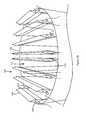
- FIG. 16is a perspective view of a series of blades for dividing an extruded object formed from the extrusion die shown in FIG. 14 into individual Z-directed components according to one example embodiment.
- FIG. 17is a top plan view of a Z-directed capacitor formed from the extrusion die shown in FIG. 14 .
- FIG. 18is a top plan view of a Z-directed capacitor according to another example embodiment.
- FIG. 19is a perspective view of a Z-directed capacitor having a pair of radial conductive traces that extend lengthwise through the part according to one example embodiment.
- FIG. 20is a perspective view of a Z-directed capacitor having a thin film insulator applied to a top surface thereof and a conductive trace applied on top of the thin film insulator according to one example embodiment.
- FIG. 21is a cross-sectional view of an extrusion die for forming a Z-directed transmission line or delay line according to one example embodiment.
- FIG. 22is a top plan view of a Z-directed differential transmission line formed from the extrusion die shown in FIG. 21 .
- FIG. 23Ais a perspective view of a spiral tool having spiraling projections that extend from an inner surface thereof according to one example embodiment.
- FIG. 23Bis a cutaway view of the spiral tool shown in FIG. 23A further illustrating one of the spiraling projections.
- FIG. 24is a cross-sectional view of an extrusion die for forming a Z-directed resistor according to one example embodiment.
- FIG. 25is a top plan view of a Z-directed resistor formed from the extrusion die shown in FIG. 24 .
- FIG. 26is a perspective view of an extrusion die for forming a Z-directed alternating plate capacitor according to one example embodiment.
- FIG. 27is a perspective view of the extrusion die shown in FIG. 26 schematically depicting a delivery system for delivering materials to the extrusion die.
- FIG. 28is a transparent perspective view of a Z-directed alternating plate capacitor formed from the extrusion die shown in FIGS. 26 and 27 .
- FIG. 29Ais a perspective view of a Z-directed component having a dome formed on an end thereof according to one example embodiment.
- FIG. 29Bis a perspective view of a Z-directed component having a chamfered end according to one example embodiment.
- FIG. 30is a perspective view of a plug for forming a taper in an end of a Z-directed component according to one example embodiment.
- FIG. 31is a perspective view of a bottom surface of a PCB having an adhesive applied thereto in contact with a side surface of a Z-directed component inserted into a mounting hole in the PCB according to one example embodiment.
- FIG. 32Ais a perspective view of a Z-directed component inserted into a mounting hole in a PCB, the Z-directed component having a conductive strip applied to a side surface thereof according to one example embodiment.
- FIG. 32Bis a side cutaway view of the Z-directed component and PCB shown in FIG. 32A .
- An X-Y-Z frame of referenceis used herein.
- the X and Y axesdescribe the plane defined by the face of a printed circuit board.
- the Z-axisdescribes a direction perpendicular to the plane of the circuit board.
- the top surface of the PCBhas a zero Z-value.
- a component with a negative Z-direction valueindicates that the component is inserted into the top surface of the PCB.
- Such a componentmay be above (extend past), flush with, or recessed below either the top surface and/or the bottom surface of the PCB.
- a component having both a positive and negative Z-direction valueindicates that the component is partially inserted into the surface of the PCB.
- the Z-directed componentsare intended to be inserted into a hole or recess in a printed circuit board.
- more than one Z-directed componentmay be inserted into a single mounting hole in the PCB, such as being stacked together or positioned side by side.
- the holemay be a through hole (a hole from the top surface through to the bottom surface), a blind hole (an opening or recess through either the top or bottom surface into an interior portion or internal layer of the PCB) or an internal cavity such that the Z-directed component is embedded within the PCB.
- the Z-directed componentis referred to as having a top surface, a bottom surface and a side surface.
- the references to top and bottom surfaces of the Z-directed componentconform to the convention used to refer to the top and bottom surfaces of the PCB.
- the side surface of a Z-directed componentextends between the top and bottom surfaces of the PCB and would be adjacent to the wall of the mounting hole in the PCB where the mounting hole is perpendicular to the face of the PCB.
- top, bottom and sideshould not be taken as limiting how a Z-directed component may be mounted into a PCB.
- the componentsare described herein as being mounted in a Z-direction, this does not mean that such components are limited to being inserted into a PCB only along the Z-axis.
- Z-directed componentsmay be mounted normal to the plane of the PCB from the top or bottom surfaces or both surfaces, mounted at an angle thereto or, depending on the thickness of the PCB and the dimensions of the Z-directed component, inserted into the edge of the PCB between the top and bottom surfaces of the PCB. Further, the Z-directed components may be inserted into the edge of the PCB even if the Z-directed component is wider than the PCB is tall as long as the Z-directed component is held in place.
- the Z-directed componentsmay be made from various combinations of materials commonly used in electronic components.
- the signal connection pathsare made from conductors, which are materials that have high conductivity. Unless otherwise stated, reference to conductivity herein refers to electrical conductivity.
- Conducting materialsinclude, but are not limited to, copper, gold, aluminum, silver, tin, lead and many others.
- the Z-directed componentsmay have areas that need to be insulated from other areas by using insulator materials that have low conductivity like plastic, glass, FR4 (epoxy & fiberglass), air, mica, ceramic and others.
- Capacitorsare typically made of two conducting plates separated by an insulator material that has a high permittivity (dielectric constant).
- Permittivityis a parameter that shows the ability to store electric fields in the materials like ceramic, mica, tantalum and others.
- a Z-directed component that is constructed as a resistorrequires materials that have properties that are between a conductor and insulator having a finite amount of resistivity, which is the reciprocal of conductivity. Materials like carbon, doped semiconductor, nichrome, tin-oxide and others are used for their resistive properties.
- Inductorsare typically made of coils of wires or conductors wrapped around a material with high permeability.
- Permeabilityis a parameter that shows the ability to store magnetic fields in the material which may include iron and alloys like nickel-zinc, manganese-zinc, nickel-iron and others.
- Transistorssuch as field effect transistors (“FETs”) are electronic devices that are made from semiconductors that behave in a nonlinear fashion and are made from silicon, germanium, gallium arsenide and others.
- Z-directed componentsmay be constructed of materials that have not been discovered or created to date.
- the body of a Z-directed componentwill in general be comprised of an insulator material unless otherwise called out in the description for a particular design of a Z-directed component.
- This materialmay possess a desired permittivity, e.g., the body of a capacitor will typically be comprised of an insulator material having a relatively high dielectric constant.
- PCBs using a Z-directed componentmay be constructed to have a single conductive layer or multiple conductive layers as is known.
- the PCBmay have conductive traces on the top surface only, on the bottom surface only, or on both the top and bottom surfaces.
- one or more intermediate internal conductive trace layersmay also be present in the PCB.
- Connections between a Z-directed component and the traces in or on a PCBmay be accomplished by soldering techniques, screening techniques, extruding techniques or plating techniques known in the art. Depending on the application, solder pastes and conductive adhesives may be used. In some configurations, compressive conductive members may be used to interconnect a Z-directed component to conductive traces found on the PCB.
- a Z-directed componentcomprises a body having a top surface, a bottom surface and a side surface, a cross-sectional shape that is insertable into a mounting hole of a given depth D within a PCB with a portion of the body comprising an insulator material. All of the embodiments described herein for Z-directed components are based on this general form.
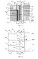
- FIGS. 1 and 2show an embodiment of a Z-directed component.
- Z-directed component 10includes a generally cylindrical body 12 having a top surface 12 t , a bottom surface 12 b , a side surface 12 s , and a length L generally corresponding to the depth D of the mounting hole.
- the length Lcan be less than, equal to or greater than the depth D.
- Z-directed component 10would in one case be below at least one of the top and bottom surfaces of the PCB and in the other it may be flush with the two surfaces of the PCB. Where length L is greater than depth D, Z-directed component 10 would not be flush mounted with at least one of the top and bottom surfaces of the PCB.
- Z-directed component 10would be capable of being used to interconnect to another component or another PCB that is positioned nearby.
- the mounting holeis typically a through-hole extending between the top and bottom surfaces of the PCB but it may also be a blind hole. When recessed below the surface of the PCB, additional resist areas may be required in the hole of the PCB to keep from plating the entire circumferential area around the hole.
- Z-directed component 10 in one formmay have at least one conductive channel 14 extending through the length of body 12 .
- top and bottom conductive traces 16 t , 16 bare provided on the top and bottom end surfaces 12 t , 12 b of body 12 and extend from respective ends of the conductive channel 14 to the edge of Z-directed component 10 .
- body 12comprises an insulator material.
- body 12 of Z-directed component 10may be made of variety of materials having different properties. These properties include being conductive, resistive, magnetic, dielectric, or semi-conductive or various combinations of properties as described herein. Examples of materials that have the properties are copper, carbon, iron, ceramic or silicon, respectively.
- Body 12 of Z-directed component 10may also comprise a number of different networks needed to operate a circuit that will be discussed later.
- One or more longitudinally extending channels or wellsmay be provided on the side surface of body 12 of Z-directed component 10 .
- the channelmay extend from one of the top surface and the bottom surface of body 12 toward the opposite surface.
- two concave side wells or channels 18 and 20are provided in the outer surface of Z-directed component 10 extending the length of body 12 . When plated or soldered, these channels allow electrical connections to be made to Z-directed component 10 , through the PCB, as well as to internal conductive layers within the PCB.
- the length of side channels 18 or 20may extend less than the entire length of body 12 .
- FIG. 2shows the same component as in FIG. 1 but with all the surfaces transparent.
- Conductive channel 14is shown as a cylinder extending through the center of Z-directed component 10 .
- Other shapesmay also be used for conductive channel 14 .
- Traces 16 t and 16 bcan be seen extending from ends 14 t and 14 b of conductive channel 14 , respectively, to the edge of body 12 . While traces 16 t and 16 b are shown as being in alignment with one another (zero degrees apart), this is not a requirement and they may be positioned as needed for a particular design. For example, traces 16 t and 16 b may be 180 degrees apart or 90 degrees apart or any other increment.
- FIGS. 3A-3Fillustrate possible body shapes for a Z-directed component.
- FIG. 3Ashows a triangular cross-sectional body 40 ;
- FIG. 3Bshows a rectangular cross-sectional body 42 ;
- FIG. 3Cshows a frusto-conical body 44 ;
- FIG. 3Dshows an ovate cross-sectional cylindrical body 46 ;
- FIG. 3Eshows a cylindrical body 48 .
- FIG. 3Fshows a stepped cylindrical body 50 where one portion 52 has a larger diameter than another portion 54 .
- the Z-directed componentmay be mounted on the surface of the PCB while having a section inserted into a mounting hole provided in the PCB.
- the edges of the Z-directed componentmay be beveled to help with aligning the Z-directed component for insertion into a mounting hole in a PCB.
- Other shapes and combinations of those illustratedmay also be used for a Z-directed component as desired.
- the channels for platingcan be of various cross-sectional shapes and lengths. The only requirement is that plating or solder material make the proper connections to the Z-directed component and corresponding conductive traces in or on the PCB.
- Side channels 18 or 20may have, for example, V-, C- or U-shaped cross-sections, semi-circular or elliptical cross-sections. Where more than one channel is provided, each channel may have the same or a different cross-sectional shape.
- FIGS. 4A-4Cillustrate three side channel shapes. In FIG. 4A , V-shaped side channels 60 are shown. In FIG. 4B , U- or C-shaped side channels 62 are shown. In FIG. 4C , wavy or irregular cross-sectional side channel shapes 65 are shown.
- the numbers of layers in a PCBvaries from being single sided to being over 22 layers and may have different overall thicknesses that range from less than 0.051 inch to over 0.093 inch or more.
- the length of the Z-directed componentwill depend on the thickness of the PCB into which it is intended to be inserted.
- the Z-directed component's lengthmay also vary depending on the intended function and tolerance of a process.
- the preferred lengthswill be where the Z-directed component is either flush with the surfaces or extends slightly beyond the surface of the PCB. This would keep the plating solution from plating completely around the interior of the PCB hole that may cause a short in some cases. It is possible to add a resist material around the interior of a PCB hole to only allow plating in the desired areas.
- a decoupling capacitorwould have lower impedance if the connection used a greater volume of copper to make the connection.
- the number of channels or conductorscan be varied from zero to any number that can maintain enough strength to take the stresses of insertion, plating, manufacturing processes and operation of the PCB in its intended environment.
- the outer surface of a Z-directed componentmay have a coating that glues it in place.
- Flanges or radial projectionsmay also be used to prevent over or under insertion of a Z-directed component into the mounting hole, particularly where the mounting hole is a through-hole.
- a surface coating materialmay also be used to promote or impede migration of the plating or solder material.
- Various locating or orienting featuresmay be provided such as a recess or projection, or a visual or magnetic indicator on an end surface of the Z-directed component.
- a connecting featuresuch as a conductive pad, a spring loaded style pogo-pin or even a simple spring may be included to add an additional electrical connection (such as frame ground) point to a PCB.
- FIG. 5Ais a Z-directed component configured as 0-port device 70 A used as a plug so that if a filter or a component is optional then the plug stops the hole from being plated. After the PCB has been manufactured, the 0-port device 70 A may be removed and another Z-directed component may be inserted, plated and connected to the circuit.
- FIGS. 5B-5Hillustrate various configurations useful for multi-terminal devices such as resistors, diodes, transistors, and/or clock circuits.
- FIG. 5Bshows a 1-port or single signal Z-directed component 70 B having a conductive channel 71 through a center portion of the component connected to top and bottom conductive traces 72 t , 72 b .
- FIG. 5Cshows a 1-port 1-channel Z-directed component 70 C where one plated side well or channel 73 is provided in addition to conductive channel 71 through the component, which is connected to top and bottom conductive traces 72 t and 72 b .
- FIG. 5Dshows a Z-directed component 70 D having two side wells 73 and 75 in addition to conductive channel 71 through the component which is connected to top and bottom traces 72 t , 72 b .
- FIG. 5Ehas three side wells 73 , 75 and 76 in addition to conductive channel 71 through the component, which is connected to top and bottom traces 72 t , 72 b .
- FIG. 5Fshows Z-directed component 70 F having two conductive channels 71 and 77 through the component each with their respective top and bottom traces 72 t , 72 b and 78 t , 78 b and no side channels or wells.
- Z-directed component 70 Fis a two signal device to be primarily used for differential signaling.
- FIG. 5Gshows a Z-directed component 70 G having one side well 73 and two conductive channels 71 and 77 each with their respective top and bottom traces 72 t , 72 b and 78 t , 78 b .
- FIG. 5Hshows Z-directed component 70 H having one conductive channel 71 with top and bottom traces 72 t , 72 b and a blind well or partial well 78 extending from the top surface along a portion of the side surface that will allow the plating material or solder to stop at a given depth.
- the number of wells and signalsis only limited by the space, required well or channel sizes.
- FIGS. 6A-Cillustrate another configuration for a Z-directed component utilizing O-rings for use in a PCB having a top and bottom conductive layer and at least one internal conductive layer.
- Z-directed component 150is shown having on its top surface 150 t , a locating feature 152 and a conductive top trace 154 t extending between a conductive channel 156 and the edge of body 150 d on its top surface 150 t .
- a conductive bottom trace(not shown) is provided on the bottom surface.
- Conductive channel 156extends through a portion of the body 150 d as previously described.
- Located on the side surface 150 s of body 150 dis a least one semi-circular channel or grove.
- a pair of axially spaced apart circumferential channels 158 a , 158 bis provided having O-rings 160 a , 160 b , respectively disposed within channels 158 a , 158 b .
- a portion of the O-rings 160 a , 160 bextend out beyond the side surface 150 s of the body 150 d .
- O-rings 160 a , 160 bwould be positioned adjacent one or more of the internal layers of the PCB to make electrical contract to one or more traces provided at that point in the mounting hole for the Z-directed component. Depending on the design employed, an O-ring would not have to be provided adjacent every internal layer.
- O-rings 160 a , 160 bmay be conductive or non-conductive depending on the design of the circuit in which they are used. O-rings 160 a , 160 b preferably would be compressive helping to secure Z-directed component 150 within the mounting hole.
- the region 162 of body 150 d intermediate O-rings 160 a , 160 bmay be comprised of different material than the regions 164 and 166 of the body 150 d outside of the O-rings. For example, if the material of region 162 is of a resistive material and O-rings 160 a , 160 b are conductive then internal circuit board traces in contact with the O-rings 160 a , 160 b see a resistive load.
- Regions 164 and 166may also be comprised of a material having different properties from each other and region 162 .
- region 164may be resistive, region 162 capacitive and region 166 inductive. Each of these regions can be electrically connected to the adjoining layers of the PCB. Further, conductive channel 156 and traces 154 t , 154 b do not need to be provided. So for the illustrated construction, between the top layer of the PCB and the first internal layer from the top, a resistive element may be present in region 164 , a capacitive element between the first internal layer and the second internal layer in region 162 and an inductive element between the second internal layer and the bottom layer of the PCB in region 166 .
- the material for regions 162 , 164 , 166may have properties selected from a group comprising conductive, resistive, magnetic, dielectric, capacitive or semi-conductive and combinations thereof.
- the designmay be extended to circuit boards having fewer or more internal layers than that described without departing from the spirit of the invention.
- regions 162 , 164 , 166may have electronic components 167 , 169 , 171 embedded therein and connected as described herein. Also, as illustrated for component 171 , a component may be found within one or more regions within the body of a Z-directed component. Internal connections may be provided from embedded components to O-rings 160 a , 160 b . Alternatively, internal connections may be provided from the embedded components to plateable pads provided on the side surface 150 s.
- a Z-directed componentmay be made of a bulk material that performs a network function or may have other parts embedded into its body.
- a Z-directed componentmay be a multi-terminal device and, therefore, may be used to perform a variety of functions including, but not limited to: transmission lines, delay lines, T filters, decoupling capacitors, inductors, common mode chokes, resistors, differential pair pass throughs, differential ferrite beads, diodes, or ESD protection devices (varistors). Combinations of these functions may be provided within one component.
- FIG. 7illustrates various example configurations for a conductive channel in a Z-directed component.
- channel 90has a region 92 intermediate the ends comprising a material having properties selected from a group comprising conductive, resistive, magnetic, dielectric, capacitive or semi-conductive properties and combinations thereof. These materials form a variety of components.
- a componentmay be inserted or embedded into region 92 with portions of the conductive channel extending from the terminals of the component.
- a capacitor 92 amay be provided in region 92 .
- a diode 92 ba transistor 92 c such as a MOSFET 92 d , a zener diode 92 e , an inductor 92 f , a surge suppressor 92 g , a resistor 92 h , a diac 92 i , a varactor 92 j and combinations of these items are further examples of materials that may be provided in region 92 of conductive channel 90 . While region 92 is shown as being centered within the conductive channel 90 , it is not limited to that location.
- one portion of the conductive channelmay be between the top surface trace and a first terminal of the device and the other portion of the conductive channel between the bottom surface trace and a second terminal of the device.
- additional conductorsmay be provided in the body of the Z-directed component to allow electrical connection to the remaining terminals or additional conductive traces may be provided within the body of the Z-directed component between the additional terminals and channels on the side surface of the body of a Z-directed component allowing electrical connection to an external conductive trace.
- Various connection configurations to a multiple terminal devicemay be used in a Z-directed component.
- FIGS. 8 and 9illustrate a Z-directed component termed a signal pass-through that is used for passing a signal trace from the top surface of a PCB to the bottom surface.
- FIG. 8shows a sectional view taken along line 8 - 8 in FIG. 9 of a PCB 200 having 4 conductive planes or layers comprising, from top to bottom, a ground (GND) plane or trace 202 , a voltage supply plane V CC 204 , a second ground GND plane 206 and a third ground GND plane or trace 208 separated by nonconductive material such as a phenolic plastic such as FR4 which is widely used as is known in the art.
- PCB 200may be used for high frequency signals.
- the top and bottom ground planes or traces 202 and 208 , respectively, on the top and bottom surfaces 212 and 214 , respectively, of PCB 200are connected to conductive traces leading up to Z-directed component 220 .
- a mounting hole 216 having a depth D in a negative Z directionis provided in PCB 200 for the flush mounting of Z-directed component 220 .
- depth Dcorresponds to the thickness of PCB 200 ; however, depth D may be less than the thickness of PCB 200 creating a blind hole therein.
- Mounting hole 216is a through-hole that is round in cross-section to accommodate Z-directed component 220 but may have cross sections to accommodate the insertion of Z-directed components having other body configurations. In other words, mounting holes are sized so that Z-directed components are insertable therein. For example, a Z-directed component having a cylindrical shape may be inserted into a square mounting hole and vice versa. In the cases where Z-directed component does not make a tight fit, resist materials will have to be added to the areas of the component and PCB where copper plating is not desired.
- Z-directed component 220is illustrated as a three lead component that is flush mounted with respect to both the top surface 212 and bottom surface 214 of PCB 200 .
- Z-directed component 220is illustrated as having a generally cylindrical body 222 of a length L.
- a center conductive channel or lead 224illustrated as being cylindrical, is shown extending the length of body 222 .
- Two concave side wells or channels 226 and 228which define the other two leads, are provided on the side surface of Z-directed component 220 extending the length of body 222 .
- Side channels 226 and 228are plated for making electrical connections to Z-directed component 220 from various layers of PCB 200 .
- V CC plane 204does not connect to Z-directed component 220 as shown by the gap 219 between V CC plane 204 and wall 217 of mounting hole 216 .
- FIG. 9illustrates a top view of Z-directed component 220 in PCB 200 .
- Three conductive traces 250 , 252 and 254lead up to the edge of wall 217 of mounting hole 216 .
- trace 252serves as a high-frequency signal trace to be passed from the top surface 212 to the bottom surface 214 of PCB 200 via Z-directed component 220 .
- Conductive traces 250 and 254serve as ground nets.
- Center lead or conductive channel 224is electrically connected to trace 252 on the top surface 212 of PCB 200 by a top trace 245 and plating bridge 230 .
- Top trace 245 on the top surface of Z-directed component 220extends from the top end 224 t of conductive channel 224 to the edge of Z-directed component 220 .
- the bottom side of Z-directed component 220 and bottom surface 214 of PCB 200is configured in a similar arrangement of traces as shown on top surface 212 of PCB 200 illustrated in FIG. 12 .
- a bottom trace on the bottom surface of Z-directed component 220extends from bottom of conductive channel 224 to the edge of Z-directed component 220 .
- a plating bridgeis used to make the electrical connection between the bottom trace and another high frequency signal trace provided on the bottom surface of PCB 200 .
- the transmission line impedance of the Z-directed componentcan be adjusted to match the PCB trace impedance by controlling the conductor sizes and distances between each conductor which improves the high speed performance of the PCB.
- wells 256 and 258 formed between wall 217 of mounting hole 216 and side channels 226 and 228allow plating material or solder pass from the top surface 212 to the bottom surface 214 electrically interconnecting traces 250 and 254 , respectively to side channels 226 and 228 , respectively, of Z-directed component 220 and also to similarly situated traces provided on the bottom surface 214 of PCB 200 interconnecting ground planes or traces 202 , 206 and 208 .
- the platingis not shown for purposes of illustrating the structure. In this embodiment, V CC plane 204 does not connect to Z-directed component 220 .
- a Z-directed signal pass through componentmay also comprise a decoupling capacitor that will allow the reference plane of a signal to switch from a ground plane, designated GND, to a voltage supply plane, designated V CC , without having a high frequency discontinuity.
- FIG. 10shows a cross-sectional view of a typical 4-layer PCB 300 with a signal trace 302 transferring between the top layer 304 and the bottom layer 306 .
- Z-directed component 310similar to that shown in FIG. 5D , having body 312 connects signal trace 302 through center conductive channel 314 .
- Z-directed component 310also comprises plated side channels 316 and 318 extending along the side surface 312 s of the body 312 .
- top 314 t and bottom 314 b of conductive channel 314are connected to conductive traces 318 t and 318 b on the top 312 t and bottom 312 b of body 312 . These, in turn, are connected to signal trace 302 via top and bottom plating bridges 330 t and 330 b .
- Side channels 316 and 318are plated to GND plane 332 and V CC plane 334 , respectively.
- Connection points 336 and 338respectively, illustrate this electrical connection.
- Schematically illustrated decoupling capacitor 350is internal to body 312 and is connected between side channels 316 and 318 .
- Decoupling capacitor 350may be a separate capacitor integrated into the body 312 of Z-directed component 310 or it can be formed by fabricating a portion of the body 312 of Z-directed component 310 from the required materials with dielectric properties between conductive surfaces.
- the path for signal trace 302is illustrated with diagonal hatching and can be seen to run from top layer 304 to bottom layer 306 .
- GND plane 332 and side channel 316are electrically connected at 336 with the signal path return indicated by the dark stippling 362 .
- V CC plane 334 and side channel 318are electrically connected at 338 with the signal path return indicated by the light stippling 364 .
- those portionsare spaced apart from the component as shown at 370 .
- the signal plane or traceis provided at the wall or edge of the opening to allow the plating material or solder to bridge therebetween as illustrated at points 330 t , 330 b , 336 , and 338 .
- the vertically hatched portion 380shows the high speed loop area between the signal trace and return current path described by the signal trace 302 and the GND plane 332 or V CC plane 334 .
- the signal trace 302 on the bottom surface 306is referenced to power plane V CC 334 that is coupled to the GND plane 332 through decoupling capacitor 350 . This coupling between the two planes will keep the high frequency impedance close to constant for the transition from one return plane to another plane of a different DC voltage.
- FIG. 11illustrates one embodiment of this technique.
- PCB 400is comprised of, from top to bottom, top ground layer 402 , internal signal layer 404 , internal signal layer 406 and bottom ground layer 408 .
- Ground layers 402 and 408are on the top and bottom surfaces 400 t and 400 b of PCB 400 .
- a mounting hole 410shown as a through-hole, extends between the top and bottom surfaces 400 t and 400 b .
- Z-directed component 420is shown flush mounted in PCB 400 .
- Z-directed component 420comprises body 422 having a center region 424 intermediate the top 422 t and bottom 422 b of body 422 and two side channels 425 and 427 on side surface 422 s.
- Center region 424is positioned within body 422 and extends a distance approximately equal to the distance separating the two internal signal layers 404 and 406 .
- Side channel 425extends from the bottom surface 422 b of body 422 to internal signal level 406 while side channel 427 extends from top surface 422 t of body 422 to internal signal level 404 .
- side channels 425 and 427extend only along a portion of side surface 422 s of body 422 .
- Conductive channel 426extends through center region 424 but does not extend to the top and bottom surfaces 422 t , 422 b of body 422 .
- Conductive channel 426has conductive traces 428 t and 428 b extending from the top 426 t and bottom 426 b of conductive channel 426 to side channels 427 and 425 , respectively. While illustrated as separate elements, conductive channel 426 and traces 428 t , 428 b may be one integrated conductor electrically interconnecting side channels 425 , 427 . As shown, conductive trace 428 b is connected to internal signal layer 406 via plated side channel 425 and well 413 while trace 428 t connects to internal signal level 404 via side channel 427 and well 415 .
- Ground layers 402 and 408are not connected to Z-directed component 420 and are spaced away from mounting hole 410 as previously described for FIGS. 8 and 10 .
- a signal on signal layer 406can be via′d to signal layer 404 (or vice versa) via Z-directed component 420 through a path extending from well 413 , side channel 425 , trace 428 b , conductive channel 426 , trace 428 t , side channel 427 , and well 415 to allow the signal to remain on the inner layers of PCB 400 with ground layers 402 and 408 providing shielding.
- FIGS. 12 and 13illustrate two additional example Z-directed components in the form of decoupling capacitors.
- a Z-directed capacitor 500is shown with a body 502 having a conductive channel 504 and two side channels 506 and 508 extending along its length similar to those previously described.
- Conductive channel 504is shown connected to a signal 526 .
- Vertically oriented interleaved partial cylindrical sheets 510 , 512 forming the plates of Z-directed capacitor 500are connected to reference voltages such as voltage V CC and ground (or any other signals requiring capacitance) and are used with intervening layers of dielectric material (not shown).
- Partial cylindrical sheet 510is connected to plated channel 506 which is connected to ground 520 .
- Partial cylindrical sheet 512is connected to plated channel 508 which is connected to supply voltage V CC 522 .
- Sheets 510 , 512may be formed of copper, aluminum or other material with high conductivity.
- the material between the partial cylindrical sheetsis a material with dielectric properties. Only one partial cylindrical sheet is shown connected to each of V CC 522 and ground 520 ; however, additional partial cylindrical sheets may be provided to achieve the desired capacitance/voltage rating.
- Center conductive channel 601extends through openings 615 in the assembled Z-directed capacitor 600 and openings 602 t and 602 b , all of which are sized to closely receive the center conductor.
- Center conductive channel 601is electrically connectable to conductive traces 603 t and 603 b on the top and bottom portions 605 t , 605 b forming a signal path for signal 626 . This connection is made by plating or soldering.
- Center conductive channel 601is connected to signal 626 via conductive trace 603 t .
- the bottom end of conductive channel 601is connected in a similar fashion to a signal trace (not shown) via conductive trace 603 b.
- Opposed openings 607 t and 608 tare provided at the edge of top portion 605 t .
- Bottom portion 605 bis of similar construction as top portion 605 t having opposed openings 607 b and 608 b provided at the edge.
- Between top and bottom portions 605 t , 605 bare a plurality of support members 610 , which provide the capacitive feature.
- Support members 610each have at least one opening 613 at their outer edge and an inner hole 615 allowing for passage of conductive channel 601 therethrough. As shown, two opposed openings 613 are provided in each support member 610 .
- the opposed openings 607 t , 607 b , 608 t , 608 b , and 613align to form opposed side channels 604 and 608 extending along the side surface of Z-directed capacitor 600 .
- Side channel 604is shown connected to reference voltage such as ground 620 and side channel 606 to another reference voltage such as V CC 622 .
- Support members 610may be fabricated from a dielectric material and may be all of the same or varying thickness allowing for choice in designing the desired properties for Z-directed capacitor 600 .
- Annular plating 617is provided on one of top and bottom surfaces of support member 610 or, if desired, on both surfaces. Annular plating is shown on the top surface of each support member but location of the annular plating can vary from support member to support member. Annular plating 617 generally conforms to the shape of the support member and extends from one of the edge openings 613 toward the other if an additional opening is provided.
- the annular plate 617is of a diameter or dimension or overall size that is less than the diameter, dimension or overall size of support member 610 on which it is affixed.
- the plate 617is described as annular, other shapes may also be used provided that the plating does not contact the center conductive channel or extend to the edge of the support member on which it is plated or otherwise affixed.
- the annular platedoes contact one of the edge openings 613 but is spaced apart from the other openings if more than one channel is present in the side surface of the body of Z-directed capacitor 600 .
- the support members 610are substantially identical except that when stacked, alternate members are rotated 180 degrees with respect to the member above or below it. This may be referred to as a 1-1 configuration. In this way, alternate members will be connected to one or the other of the two side channels. As shown in FIG. 13 , the annular plating on the upper one of the two support members 610 is connected to side channel 608 and voltage V CC 622 while the annular plating on the lower one of the two support members 610 is connected to side channel 604 and ground 620 . Other support member arrangements may also be used such as having two adjacent members connected to the same channel with the next support member being connected to the opposite channel which may be referred to as a 2-1 configuration.
- Other configurationsmay include 2-2, 3-1 and are a matter of design choice.
- the desired capacitance or voltage ratingdetermines the number of support members that are inserted between top and bottom portions 605 t , 605 b .
- dielectric memberscomprised of dielectric material and similarly shaped to support members 610 may be interleaved with support members 610 .
- only a single channelmay be used or more channels may be provided and/or the annular plating may be brought into contact with the center conductive channel and not in contact with the side channels.
- the embodiments for Z-directed capacitorsare for purposes of illustration and are not meant to be limiting.
- a second conductive channelmay be provided in parallel with the first conductive channel that is disposed within the conductive plates to create a differential decoupling capacitor.
- Another embodiment of a Z-directed capacitorcan be constructed from FIG. 12 or FIG. 13 by connecting the center conductive channel to one of the reference voltages at each support member that also has its annular plating connected to the same reference voltage. This may be accomplished simply by connecting the conductive channel to the annular plating as schematically illustrated by the jumper 621 .
- the annular opening 619 in the annular plate 617would be sized so that the annular plate and conductive channel 601 would be electrically connected. This component may be placed directly below a power pin or ball of an integrated circuit or other surface mounted component for optimum decoupling placement.
- Z-directed signal pass-through components illustrated in FIGS. 8-11 and the Z-directed decoupling capacitors illustrated in FIGS. 12 and 13provide merely a few example applications of a Z-directed component.
- Those skilled in the artwill appreciate that various other types of Z-directed components may be utilized including, but not limited to, transmission lines, delay lines, T filters, decoupling capacitors, inductors, common mode chokes, resistors, differential pair pass throughs, differential ferrite beads, diodes, or ESD protection devices (varistors).
- a continuous extrusion process for manufacturing the Z-directed components on a commercial scaleis provided.
- at least two different materialsare extruded simultaneously to form the Z-directed component.
- This processis particularly useful where the materials forming the Z-directed component extend in a lengthwise direction within the component.
- a variety of different Z-directed componentsare contemplated herein. Accordingly, it will be appreciated that the specific materials used will depend on the Z-directed component desired. Signal paths will be formed from a conductive material. Resistive materials may also be used as desired.
- a dielectric materialmay be used that has a relative permittivity from about 3, e.g., polymers, to over 10,000, e.g., barium titanate (BaTiO 3 ).
- a material with a relatively high dielectric valuemay be used in a Z-directed decoupling capacitor and a material with a relatively low dielectric value may be used in a Z-directed signal pass-through component. If a Z-directed component is desired to have an inductive function or a delay line then a ferrite material may be selected that has a low or high relative permeability with a range of about 1 to about 50,000.
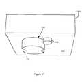
- extrusion die 700for forming a Z-directed component in the form of a decoupling capacitor according to one example embodiment is illustrated.
- the Z-directed capacitor formed from extrusion die 700is composed of conductive material and dielectric material. As needed, a binder material may also be included as is known in the art.
- Extrusion die 700includes a chamber 702 having an inlet 704 and an outlet 706 for passing material therethrough. Chamber 702 is divided into a plurality of channels 708 that are separated from one another by one or more barriers 710 to permit simultaneous extrusion of multiple materials. The channels 708 are arranged in predetermined positions that define the structure of the Z-directed component.
- a chamber 702 having a circular cross-sectionis used to form a generally cylindrical Z-directed component; however, as discussed above, many different shapes may be used.
- the Z-directed componentis formed by simultaneously forcing the desired materials into their corresponding channels 708 at inlet 704 of extrusion die 700 , which causes the materials to take on the respective shapes of channels 708 .
- the materialsmay be pressed into channels 708 using a ram, injection press or extruder screw (not shown).
- a direct extrusion processmay be used where extrusion die 700 is held stationary and the ram is moved towards it or an indirect extrusion process may be used where the ram is held stationary and extrusion die 700 is moved towards it.
- a combination of the twomay be also used where the ram and die 700 are moved towards each other.
- a hydrostatic extrusion processmay also be used where fluid pressure forces the materials through die 700 .
- Extrusion die 700may be oriented horizontally, vertically or at any suitable angle thereto. Any conventional drive may be applied to provide the extruding force including a mechanical or hydraulic drive. The desired materials are forced through die 700 in a continuous manner so that substantially an entire component (or more than one component) is extruded at once. Where more than one component is extruded at once, the extruded object exiting chamber 702 may then be divided into individual components as discussed in greater detail below.
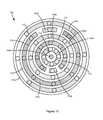
- FIG. 15shows a cross section of extrusion die 700 taken near inlet 704 .
- the channels 708 that are filled with conductive materialare indicated with a medium cross hatched fill and the channels 708 that are filled with dielectric material are indicated with a light dotted fill.
- Barriers 710 of extrusion die 700are shown in cross-section without a fill.
- the small circles 712 shown in FIG. 15indicate locations at inlet 704 where the desired materials may be pressed into chamber 702 .
- the size and number of inlet ports 712are selected to provide predetermined volumetric material flow rates through chamber 702 .
- a center conductive channel in the Z-directed capacitoris formed in channel 708 a .
- Channel 708 acan also be used to form a signal trace, as desired.
- Two concentric conductive plates that surround the center conductive channelare formed in channels 708 b and 708 c .
- the conductive layersare isolated from each other by three layers of dielectric material.
- the dielectric layersare formed around each of the conductive layers in channels 708 d , 708 e and 708 f .
- a dielectric divideris formed in each of the concentric conductive plates to make a bridge path that will be used to connect alternating conductive traces on the top and/or bottom of the component.
- the dielectric dividersare formed by channels 708 g and 708 h in extrusion die 700 .
- the diameter of chamber 702reduces from inlet 704 to outlet 706 .
- Each of the barriers 710correspondingly tapers from inlet 704 to outlet 706 such that at a location near inlet 704 (shown in FIG. 15 ), barriers 710 are thicker than they are near outlet 706 (shown in FIG. 14 ).
- the various materialsare isolated from one another by barriers 710 when they are first introduced into chamber 702 .
- Laminar flowis desired through chamber 702 in order to fill each channel 708 and form a substantially uniform part that is free of air gaps or other irregularities.
- the reduction in diameter of chamber 702 and the corresponding taper of barriers 710cause the materials to fill their respective channels 708 and promote laminar flow therethrough.
- any remaining length of chamber 702 prior to outlet 706has a constant diameter (as shown in dashed lines in FIG. 14 ) in order to maintain the shape of the extruded object and the relative positions of the various materials therein.
- the diameter of chamber 702may continue to narrow in order to shrink the component to its final dimensions so long as the positioning of the various materials making up the component relative to each other is not disturbed.
- a movable elementsuch as a plug or rod, may be used to support the downstream end of the extruded object as it advances to help prevent it from losing its shape. For instance, where the extrusion process is performed in a vertically downward direction, a plug that lowers according to the speed of extrusion may be used to support the extruded object from below to maintain the shape of the extruded object.
- the extruded objectcan be partially fired in order to improve the strength of the materials and to ensure that the component will remain intact.
- Moderate heatmay also be applied to cure the binder material. Heating elements can be embedded into the walls of a chamber downstream from the extrusion output, which may either be attached to the extrusion die or form a unitary part of the extrusion die, in order to supply a desired temperature profile to the extruded object.
- a full firing processmay be performed at this time.
- the extruded objectis divided into individual Z-directed components according to the desired length(s) of the Z-directed component(s).
- FIG. 16shows a segment of an extruded object 720 ready to be cut.
- One optionis to use a series of blades 722 spaced according to the desired component lengths.
- the componentsrange in length from about 0.5 mil to about 62 mil (about 0.0127 mm to about 1.57 mm), including all increments and values therebetween, depending on the PCB used and the desired mounting position of the Z-directed component.
- Another optionis to cut the extruded object 720 using multiple passes of a single blade. In this embodiment, the length of each component is determined by controlling the timing of each pass of the blade.
- Each componentmay have substantially the same length or different lengths may be used.
- a feedback mechanismmay be used to adjust the timing of the cuts in order to account for parameters that may change with blade usage, such as the kerf of the blade.
- the extruded objectmay be in an unfired, a partially fired or a fully fired state when it is divided into separate components. It will be appreciated that a partially fired state is preferred.
- When extruded object 720 is cut in an unfired stateit may be difficult to ensure that extruded object 720 will retain its shape.
- each Z-directed componentmay be extruded individually. However, this may still require each extruded component to be cut to its precise length.
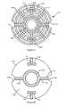
- FIG. 17shows a top plan view of a Z-directed capacitor 730 formed using the example extrusion die 700 shown in FIGS. 14 and 15 .
- the diagonal hatchingindicates those areas that are composed of conductive material.
- the remainder of the componentis composed of dielectric material.
- Capacitor 730includes a center conductor 732 running lengthwise through the part that is formed by channel 708 a .
- Capacitor 730also includes a pair of concentric conductive plates 734 , 736 spaced radially from conductor 732 running lengthwise through the part that are formed by channels 708 b , 708 c , respectively.
- a conductive trace 744is added to a top and/or bottom surface of capacitor 730 that connects center conductor 732 to outer conductive plate 736 and to an edge of the part to provide a connection with a corresponding trace on the PCB.
- Trace 744passes through a dielectric divider 748 formed by channel 708 g in order to avoid connection with middle conductive plate 734 .
- a conductive trace 746is added to connect middle conductive plate 734 to an edge of the capacitor 730 to provide a connection with another trace on the PCB.
- Trace 746passes through a dielectric divider 750 formed by channel 708 f in order to avoid connection with outer conductive plate 736 .
- center conductor 732 and outer conductive plate 736are connected to a supply voltage V CC and middle conductive plate 734 is connected to ground voltage GND although this configuration can be reversed as desired.
- Traces 744 , 746can be applied when the Z-directed component is fabricated or after the Z-directed component is inserted into the mounting hole in the PCB when the PCB is plated.
- the Z-directed capacitormay have any number of conductive plates depending on the desired capacitance of the part.
- FIG. 18shows a Z-directed capacitor 800 having a center conductor 802 and four concentric conductive plates 804 , 806 , 808 , 810 spaced outwardly therefrom.
- Trace 812is formed on a top surface of capacitor 800 that connects center conductor 802 and conductive plates 806 and 810 to an edge of the part for connection with a trace on the PCB.
- Trace 814is formed on the top surface of capacitor 800 that connects conductive plates 804 and 808 to an edge of capacitor 800 for connection with the PCB.
- dielectric materialisolates center conductor 802 and conductive plates 804 , 806 , 808 , 810 from each other and creates a bridge for traces 812 , 814 . It will be appreciated that the number and arrangement of conductive and dielectric layers may be altered simply by changing the configuration of the extrusion die used.
- FIG. 19shows a Z-directed capacitor 900 that has a similar layout to Z-directed capacitor 700 shown in FIG. 17 except that radial conductive traces 902 , 904 extend through the length of the part.
- traces 902 , 904are formed by altering the configuration of the channels in the extrusion die so that traces 902 , 904 are extruded within the part. Traces 902 , 904 are each positioned in a respective side channel 906 , 908 in capacitor 900 .
- traces 902 , 904are exposed on a side surface 900 s of capacitor 900 along the entire length of the part.
- traces 902 , 904may be used to establish a connection not only with the top or bottom surface of the PCB but also an intermediate layer of the PCB as desired.
- a thin film resist layeris added to a top and/or bottom surface of the component in order to prevent plating material from interfering with the conductive paths present on the top or bottom surface of the Z-directed component when the PCB is plated.
- the connection between the component and the PCBmay be made by plating side channels, such as side channels 906 , 908 , of the Z-directed component and connecting them to a trace on the PCB rather than using a trace on the top or bottom surface of the component.
- FIG. 20illustrates a Z-directed capacitor 1000 having a thin film insulator 1002 screened across a top surface thereof.
- the filmis screened such that a small hole 1004 is provided in insulator 1002 in order to permit plating to a center conductor 1006 that extends the length of capacitor 1000 .
- a conductive trace 1008is applied across insulator 1002 that connects center conductor 1006 to an edge of the part. Trace 1008 from center conductor 1006 can be applied when the Z-directed component is fabricated or after the Z-directed component is inserted into the mounting hole in the PCB when the PCB is plated.
- Capacitor 1000also includes a pair of concentric conductive plates 1010 , 1012 extruded through the part. In this embodiment, center conductor 1006 is isolated from concentric conductive plates 1010 , 1012 by dielectric material.
- Conductive traces 1014 , 1016also extend through the length of the part and are exposed along a side surface 1000 s of capacitor 1000 in side channels 1018 , 1020 , respectively. Traces 1014 , 1016 extend radially from and connect conductive plates 1010 , 1012 , respectively, to an edge of the component. Conductive plates 1010 , 1012 and the radial portions of traces 1014 , 1016 are covered on the top surface of the part by insulator 1002 and are therefore shown in dashed lines. In this manner, insulator 1002 prevents the signal (Signal) sent to center conductor 1006 via trace 1008 from shorting either the supply voltage (V CC ) or the ground (GND). Trace 1008 can be connected to a corresponding trace on a top surface of the PCB and traces 1014 , 1016 can be connected to the PCB anywhere along side surface 1000 s of capacitor 1000 .
- FIG. 21illustrates a cross-section of another example extrusion die 1100 for forming a Z-directed transmission line or delay line.
- Die 1100includes a plurality of channels 1108 therein separated by barriers 1110 .
- the same fill convention used in FIG. 14is used in FIG. 21 .
- the channels 1108 that are filled with conductive materialare indicated with a medium cross hatched fill and the channels 1108 that are filled with dielectric material are indicated with a light dotted fill.
- Barriers 1110 of extrusion die 1100are shown without a fill.
- the small circles 1112 shown in FIG. 21indicate locations where the desired materials may be pressed into a chamber 1102 of die 1100 .
- FIG. 22shows a top plan view of a Z-directed differential transmission line 1120 formed using extrusion die 1100 shown in FIG. 21 .
- the same fill convention used in FIG. 17is used in FIG. 22 .
- the diagonal hatching in FIG. 22indicates those areas that are composed of conductive material.
- the remainder of the componentis composed of dielectric material.
- Transmission line 1120includes a pair of conductors 1122 , 1124 formed from channels 1108 b , 1108 c , respectively, that run lengthwise through the part.
- Transmission line 1120also includes a ground (or reference) conductor 1126 having a circular portion 1126 a and a pair of radial extensions 1126 b , 1126 c that connect to corresponding side channels 1128 , 1130 in the part.
- Conductor 1126is formed by channel 1108 a of extrusion die 1100 . Side channels 1128 , 1130 are formed by scalloped portions 1112 , 1114 , respectively. Conductors 1122 , 1124 , 1126 are separated from each other by a dielectric material 1132 such as ceramic. Conductive traces 1134 , 1136 are applied to the top surface of the component to provide a connection for conductor 1122 , 1124 . Conductors 1122 , 1124 form a differential pair. Since transmission line 1120 includes a reference conductor 1126 , the two differential signals are not highly coupled. However, conductor 1126 could be replaced with the dielectric material and the differential signals would become highly coupled.
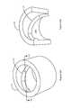
- the extruded objectmay be forced through a spiral tool 1150 that lengthens the path of conductors 1122 , 1124 relative to the length of the component.
- Spiral tool 1150includes a pair of spiraling projections 1152 that extend from an inner surface 1150 s thereof.
- FIG. 23Billustrates a cross-section of spiral tool 1150 that more clearly illustrates one of the projections 1152 therein.
- projections 1152form corresponding side channels in the component and cause the extruded object to twist as it advances. This causes conductors 1122 , 1124 to twist into a double helix configuration. Again, center conductor 1126 can be omitted as desired.
- Spiral tool 1150can be used to alter the relative positions of corresponding traces on the top and bottom surfaces of the component such that a trace on the top surface of the component can be angled with respect to a corresponding trace on the bottom surface of the component.
- spiral tool 1150can also be used to create an inductor.
- a single conductorsuch as conductor 1122 or conductor 1124 can be formed in a twisted pattern that can be used as a single wire inductor.
- the remainder of the Z-directed componentwill be composed of a material having a relatively high permeability.
- a transformercan be formed. In this embodiment, by driving current through one of the conductors 1122 or 1124 (the primary coil), energy is magnetically coupled to the second conductor (the secondary coil) as an output.
- FIG. 24illustrates a cross-section of another example extrusion die 1200 for forming a Z-directed resistor.
- Die 1200includes a plurality of channels 1208 therein separated by barriers 1210 . The same fill convention used in FIGS. 14 and 21 is used in FIG. 24 . Specifically, the channel 1208 that is filled with dielectric material is indicated with a light dotted fill. The channel 1208 that is filled with resistive material is indicated with a heavy cross hatched fill. Barriers 1210 of extrusion die 1200 are shown without a fill. The small circles 1212 shown in FIG. 24 indicate locations where the desired materials may be pressed into a chamber 1202 of die 1200 . Die 1200 includes a channel 1208 a for forming a resistive path through the length of the component and a channel 1208 b for providing dielectric material around the resistive path.
- FIG. 25shows a top plan view of a Z-directed resistor 1220 formed using extrusion die 1200 shown in FIG. 24 .
- the same fill convention used in FIGS. 17 and 22is used in FIG. 25 .
- the diagonal hatching in FIG. 22indicates those areas that are composed of conductive material.
- the heavy crossed hatchingindicates those areas that are composed of resistive material.
- the remainder of the componentis composed of dielectric material.
- Resistor 1220includes a resistive path 1222 that runs lengthwise through the part formed by channel 1208 a .
- Dielectric material 1224such as ceramic, formed by channel 1208 b surrounds resistive path 1222 .
- Conductive trace 1226is applied to the top and/or bottom surface of the component to provide a connection to resistive path 1222 . It will be appreciated that the resistance imparted by resistor 1220 may be altered as desired by changing the diameter of channel 1208 a in die 1200 in order to correspondingly alter the diameter of resistive path 1222 .
- Extrusion die 1300for forming an alternating plate capacitor according to one example embodiment is shown.
- the timing of extrusion of the various materialsis varied in order to stagger them within the Z-directed component.
- Extrusion die 1300includes a chamber 1302 having an inlet 1304 and an outlet (not shown).
- a plurality of slats 1306are positioned at inlet 1304 or downstream therefrom.
- Each slat 1306includes an inlet 1308 that receives material from a supply source through a corresponding pipe or tube 1332 .
- Each slat 1306also includes an outlet 1310 that emits material into die 1300 in the downstream direction of extrusion, which is downward in the embodiment shown in FIGS. 26 and 27 .
- One or more materialsis supplied to the inlet 1308 of each slat 1306 by a delivery system 1330 that includes a switch to control which material is being emitted by a particular slat 1306 .
- FIG. 28shows a Z-directed alternating plate capacitor 1320 formed using the example extrusion die 1300 shown in FIGS. 26 and 27 as discussed in greater detail below.
- capacitor 1320is shown with a transparent body in FIG. 28 .
- Capacitor 1320includes a plurality of conductive plates 1322 extending lengthwise within the component. Plates 1322 are divided into two sets 1322 a , 1322 b that are spaced from each other in an alternating relationship. Each of the first set 1322 a of plates 1322 extends to a bottom surface 1320 b of capacitor 1320 but is spaced from a top surface 1320 t thereof.
- each of the second set 1322 b of plates 1322extends to top surface 1320 t but is spaced from bottom surface 1320 b .
- the body of capacitor 1320is formed from dielectric material.
- Capacitor 1320includes a first conductive trace 1324 along bottom surface 1320 b that connects with each of the first set 1322 a of plates 1322 but not the second set 1322 b of plates 1322 and a second conductive trace 1326 along top surface 1320 t that connects with each of the second set 1322 b of plates 1322 but not the first set 1322 a of plates 1322 .
- trace 1324 and first set 1322 a of plates 1322are connected to a supply voltage V CC and trace 1326 and second set 1322 b of plates 1322 are connected to ground voltage GND although this configuration can be reversed as desired.
- slats 1306are disposed relative to chamber 1302 according to the desired positions of conductive plates 1322 .
- Dielectric materialis forced into inlet 1304 of chamber 1302 and around slats 1306 .
- either conductive material or additional dielectric materialis dispensed from outlets 1310 of slats 1306 depending on whether the slat 1306 corresponds with one of the first set 1322 a of plates 1322 or the second set 1322 b of plates 1322 .
- a first set 1306 a of slats 1306corresponds with first set 1322 a of plates 1322 and a second set 1306 b of slats 1306 corresponds with second set 1322 b of plates 1322 .
- tubes 1332 of delivery system 1330are divided into two sets 1332 a , 1332 b .
- first set 1332 a of tubes 1332is shown in dashed lines and second set 1332 b is shown in solid lines.
- First set 1332 a of tubes 1332supplies material to first set 1306 a of slats 1306 , which corresponds with first set 1322 a of plates 1322 .
- Second set 1332 b of tubes 1332supplies material to second set 1306 b of slats 1306 , which corresponds with second set 1322 b of plates 1322 .
- each tube 1332has substantially the same length.
- Both sets 1332 a , 1332 b of tubes 1332receive material from a manifold 1334 .
- a valve 1336such as a three-port valve (e.g., an L-shaped three-way ball valve), determines whether conductive material, dielectric material or neither is supplied to manifold 1334 .
- each of the first set 1332 a of tubes 1332is connected to a portion of manifold 1334 that is upstream from the connection between manifold 1334 and second set 1332 b of tubes 1332 . This causes first set 1332 a of tubes 1332 to receive material before second set 1332 b does.
- first set 1306 a of slats 1306receives the new material before second set 1306 b of slats 1306 does thereby creating the desired stagger between sets 1322 a , 1322 b of plates 1322 .
- tubes 1332are all the same length, first set 1306 a of slats 1306 emits material into chamber 1302 in unison and then, after the delay that results from the respective placement of tubes 1332 on manifold 1334 expires, second set 1306 b of slats 1306 emits the same material in unison to create the staggered pattern of plates 1322 shown in FIG.
- first set 1306 a of slats 1306first emits conductive material so that the corresponding first set 1322 a of conductive plates 1322 extends to bottom surface 1320 b of the part until the end of extrusion is near at which point first set 1306 a of slats 1306 switches to dielectric material so that the plates 1322 are spaced from top surface 1320 t .
- second set 1306 b of slats 1306first emits dielectric material so that the corresponding second set 1322 b of conductive plates 1322 are spaced from bottom surface 1320 b of the part and then, when the delay expires, second set 1306 b of slats 1306 switches to conductive material so that the plate 1322 extends to top surface 1320 t.
- conductive traces 1324 , 1326are added to top and bottom surfaces, respectively, as discussed above. Traces 1324 , 1326 can be applied when the Z-directed component is fabricated or after the Z-directed component is inserted into the mounting hole in the PCB when the PCB is plated.
- FIG. 27is intended to provide an example of a suitable configuration for creating the desired material delay and resulting stagger between plates 1322 . It will be appreciated that a number of different configurations of tubes 1332 , valves 1336 and manifolds 1334 may be used to facilitate material flow into each slat 1306 and that the timing of material flow and/or the lengths of the material paths may be adjusted to create the desired delay. One alternative is to use a valve 1336 and corresponding manifold 1334 specific to each set 1306 a , 1306 b of slats 1306 .
- the stagger between plates 1322can be created by setting a delay between the valve 1336 for first set 1306 a of slats 1306 and the valve 1336 for second set 1306 b of slats 1306 .
- Another optionis to provide each slat 1306 with its own valve 1336 and feedpath from the sources of conductive material and dielectric material and to control each slat 1306 individually.
- Yet another option to create the desired stagger between plates 1322is to position one set of slats 1306 , such as first set 1306 a , upstream from another set, such as second set 1306 b , and to dispense material from each slat at the same time.
- a chamfer, dome or other form of taper or lead-in of at least one of the top and bottom edge of the Z-directed componentis desired in order to ease insertion of the Z-directed component into the mounting hole in the PCB.
- FIG. 29Ashows a Z-directed component 1400 having a dome 1402 formed on an end thereof.
- FIG. 29Bshows a Z-directed component 1404 having a chamfered end 1406 .
- the dome 1402 or chamfer 1406may be part of the component or attached thereto.
- the dome 1402 or chamfer 1406is a separate part that is partially inserted into the mounting hole in the PCB.
- the Z-directed componentis then inserted behind the dome 1402 or chamfer 1406 to push it through the mounting hole causing the dome 1402 or chamfer 1406 to expand the mounting hole and prevent the component from cutting or tearing the PCB.
- the dome 1402 or chamfer 1406may be configured to remain attached to the Z-directed component following insertion into the mounting hole in the PCB or it may be used to facilitate insertion and then removed.
- One method for forming the desired taper as part of the Z-directed componentutilizes a plug 1420 having a recess 1422 formed in an end 1424 thereof having a tapered rim 1426 around a periphery of recess 1422 as shown in FIG. 30 .
- Tapered rim 1426is chamfered in the example embodiment illustrated; however, a domed, elliptical or rounded rim may also be used depending on the shape of the taper desired.
- Plug 1420is used to compress the component in a constraining plate having a cavity for retaining the component therein.
- the end of the partis reflowed to have the desired geometry and the conductive path(s) on the end of the part are allowed to continue across or through the corresponding taper formed on the end of the part.
- the tapered end portion of the partcan then be used to facilitate board to board electrical connections in multi-PCB applications.
- the Z-directed componentAfter the Z-directed component has been formed, a firing process is applied to cure the part if it has not been done so already. The firing process solidifies the part and shrinks it to its final dimensions. At this point, the Z-directed component can be tested for yield and performance and any additional processes may be performed as desired. For example, in some instances, the heating step may cause burrs to form. Accordingly, in some embodiments, the Z-directed components are tumbled with various abrasive agents to smooth the corners and edges of the part. Further, resist areas may be added to the Z-directed component to keep the conductive materials from sticking to areas that are not intended to be conductive. Glue areas may be applied to the component to assist with retaining it in the PCB. Visible markings and/or locating features may be added to the Z-directed component to assist with assembly into the PCB.
- the Z-directed componentis ready to be inserted into the mounting hole of the PCB.
- the componentmay be mounted normal to the plane of the PCB from the top or bottom surfaces or both surfaces, mounted at an angle thereto or inserted into the edge of the PCB between the top and bottom surfaces of the PCB.
- the Z-directed componentis press fit into the mounting hole. This press fit may be in the form of an interference fit between the component and the mounting hole.
- a conductive plating bridgemay be applied to connect one or more traces on the top and/or bottom surface of the component to a corresponding trace on the PCB.
- additional conductive platingmay be applied to these side channels to form the desired signal connections between the Z-directed component and the PCB.
- an adhesive 1506is applied to a surface 1508 of PCB 1504 external to mounting hole 1502 .
- Adhesive 1506is positioned to contact a surface of Z-directed component 1500 when it is inserted into mounting hole 1502 in order to fix the location of Z-directed component 1500 and prevent it from rotating or translating out of position.
- a conductive strip 1512is formed along a side surface 1510 s of a Z-directed component 1510 .
- Conductive strip 1512runs along side surface 1510 s to either the top or bottom surface of Z-directed component 1510 .
- Conductive strip 1512may be applied after the Z-directed component 1510 is formed. In the example embodiment illustrated, conductive strip 1512 runs along side surface 1510 s to a top surface 1510 t of Z-directed component 1510 .
- conductive strip 1512forms a bridge between a trace 1514 on the respective top or bottom surface of Z-directed component 1510 and a trace 1516 on a PCB 1518 when the top or bottom surface of the Z-directed component extends past the corresponding top or bottom surface of the PCB.
- trace 1514 on Z-directed component 1510is able to connect to trace 1516 on PCB 1518 even if the top or bottom surface of Z-directed component 1510 is not flush with the corresponding top or bottom surface of PCB 1518 .
- conductive strip 1512runs from top surface 1510 t of Z-directed component 1510 to a point along side surface 1510 s that is below the top surface of the PCB 1518 .
- conductive strip 1512extends into the side of Z-directed component 1510 both to decrease its resistance and to ensure that it is not removed if another feature such as a taper is later applied to Z-directed component 1510 .
Landscapes
- Engineering & Computer Science (AREA)
- Microelectronics & Electronic Packaging (AREA)
- Power Engineering (AREA)
- Manufacturing & Machinery (AREA)
- Mechanical Engineering (AREA)
- Physics & Mathematics (AREA)
- Electromagnetism (AREA)
- Chemical & Material Sciences (AREA)
- Ceramic Engineering (AREA)
- Structural Engineering (AREA)
- Structures For Mounting Electric Components On Printed Circuit Boards (AREA)
- Structure Of Printed Boards (AREA)
Abstract
Description
- This patent application is a divisional application of U.S. patent application Ser. No. 13/284,084, filed Oct. 28, 2011, entitled “Continuous Extrusion Process for Manufacturing a Z-Directed Component for a Printed Circuit Board.” This patent application is related to U.S. patent application Ser. No. 13/222,748, filed Aug. 31, 2011, entitled “Die Press Process for Manufacturing a Z-Directed Component for a Printed Circuit Board,” U.S. patent application Ser. No. 13/222,418, filed Aug. 31, 2011, entitled “Screening Process for Manufacturing a Z-Directed Component for a Printed Circuit Board,” U.S. patent application Ser. No. 13/222,376, filed Aug. 31, 2011, entitled “Spin Coat Process for Manufacturing a Z-Directed Component for a Printed Circuit Board,” and U.S. patent application Ser. No. 13/250,812, filed Sep. 30, 2011, entitled “Extrusion Process for Manufacturing a Z-Directed Component for a Printed Circuit Board,” which are assigned to the assignee of the present application.
- 1. Field of the Disclosure
- The present invention relates generally to processes for manufacturing printed circuit board components and more particularly to a continuous extrusion process for manufacturing a Z-directed component for a printed circuit board.
- 2. Description of the Related Art
- The following co-pending United States patent applications, which are assigned to the assignee of the present application, describe various “Z-directed” components that are intended to be embedded or inserted into a printed circuit board (“PCB”): Ser. No. 12/508,131 entitled “Z-Directed Components for Printed Circuit Boards,” Ser. No. 12/508,145 entitled “Z-Directed Pass-Through Components for Printed Circuit Boards,” Ser. No. 12/508,158 entitled “Z-Directed Capacitor Components for Printed Circuit Boards,” Ser. No. 12/508,188 entitled “Z-Directed Delay Line Components for Printed Circuit Boards,” Ser. No. 12/508,199 entitled “Z-Directed Filter Components for Printed Circuit Boards,” Ser. No. 12/508,204 entitled “Z-Directed Ferrite Bead Components for Printed Circuit Boards,” Ser. No. 12/508,215 entitled “Z-Directed Switch Components for Printed Circuit Boards,” Ser. No. 12/508,236 entitled “Z-Directed Connector Components for Printed Circuit Boards,” and Ser. No. 12/508,248 entitled “Z-Directed Variable Value Components for Printed Circuit Boards.”
- As densities of components for printed circuit boards have increased and higher frequencies of operation are used, some circuits' designs have become very difficult to achieve. The Z-directed components described in the foregoing patent applications are designed to improve the component densities and frequencies of operation. The Z-directed components occupy less space on the surface of a PCB and for high frequency circuits, e.g. clock rates greater than 1 GHz, allow for higher frequency of operation. The foregoing patent applications describe various types of Z-directed components including, but not limited to, capacitors, delay lines, transistors, switches, and connectors. A process that permits mass production of these components on a commercial scale is desired.
- A method for manufacturing a Z-directed component for insertion into a mounting hole in a printed circuit board according to one example embodiment includes simultaneously extruding a plurality of materials according to the structure of the Z-directed component to form an extruded object and forming the Z-directed component from the extruded object.
- A method for manufacturing a plurality of Z-directed components each for insertion into a respective mounting hole in a printed circuit board according to another example embodiment includes continuously extruding a plurality of materials in a lengthwise direction according to the structure of the Z-directed component to form an extruded object. The extruded object is divided into individual Z-directed components and each Z-directed component is cured.
- A method for manufacturing a Z-directed component for insertion into a mounting hole in a printed circuit board according to another example embodiment includes simultaneously extruding a plurality of materials according to the structure of the Z-directed component to form an extruded object. The timing of extrusion between predetermined sections of one of the materials is varied in order to stagger the sections in the extruded object. The Z-directed component is formed from the extruded object.
- The above-mentioned and other features and advantages of the various embodiments, and the manner of attaining them, will become more apparent and will be better understood by reference to the accompanying drawings.
FIG. 1 is a perspective view of a Z-directed component according to one example embodiment.FIG. 2 is a transparent perspective view of the Z-directed component shown inFIG. 1 illustrating the internal arrangement of elements of the Z-directed component.FIGS. 3A-3F are perspective views showing various example shapes for the body of a Z-directed component.FIGS. 4A-4C are perspective views showing various example side channel configurations for a Z-directed component.FIGS. 5A-5H are perspective views showing various example channel configurations for the body of a Z-directed component.FIG. 6A is a perspective view of a Z-directed component having O-rings for connecting to internal layers of a PCB and having a body having regions comprised of similar and/or dissimilar materials according to one example embodiment.FIG. 6B is a top plan view of the Z-directed component shown inFIG. 6A .FIG. 6C is a schematic side elevation view of the Z-directed component shown inFIG. 6A .FIG. 7 is a schematic illustration of various example elements or electronic components that may be provided within the body of a Z-directed component in series with a conductive channel.FIG. 8 is a schematic cross-sectional view of a Z-directed component flush mounted in a PCB showing conductive traces and connections to the Z-directed component according to one example embodiment.FIG. 9 is a top plan view of the Z-directed component and PCB shown inFIG. 8 .FIG. 10 is a schematic cross-sectional view of a Z-directed component flush mounted in a PCB showing ground loops for the Z-directed component with the Z-directed component further having a decoupling capacitor within its body according to one example embodiment.FIG. 11 is a schematic cross-sectional view of a Z-directed component flush mounted in a PCB showing a Z-directed component for transferring a signal trace from one internal layer of a PCB to another internal layer of that PCB according to one example embodiment.FIG. 12 is a perspective view of a Z-directed capacitor having semi-cylindrical sheets according to one example embodiment.FIG. 13 is an exploded view of another embodiment of a Z-directed capacitor having stacked discs according to one example embodiment.FIG. 14 is a schematic view of an extrusion die for forming a Z-directed component according to one example embodiment.FIG. 15 is a cross-sectional view of the extrusion die shown inFIG. 14 showing a plurality of channels therein.FIG. 16 is a perspective view of a series of blades for dividing an extruded object formed from the extrusion die shown inFIG. 14 into individual Z-directed components according to one example embodiment.FIG. 17 is a top plan view of a Z-directed capacitor formed from the extrusion die shown inFIG. 14 .FIG. 18 is a top plan view of a Z-directed capacitor according to another example embodiment.FIG. 19 is a perspective view of a Z-directed capacitor having a pair of radial conductive traces that extend lengthwise through the part according to one example embodiment.FIG. 20 is a perspective view of a Z-directed capacitor having a thin film insulator applied to a top surface thereof and a conductive trace applied on top of the thin film insulator according to one example embodiment.FIG. 21 is a cross-sectional view of an extrusion die for forming a Z-directed transmission line or delay line according to one example embodiment.FIG. 22 is a top plan view of a Z-directed differential transmission line formed from the extrusion die shown inFIG. 21 .FIG. 23A is a perspective view of a spiral tool having spiraling projections that extend from an inner surface thereof according to one example embodiment.FIG. 23B is a cutaway view of the spiral tool shown inFIG. 23A further illustrating one of the spiraling projections.FIG. 24 is a cross-sectional view of an extrusion die for forming a Z-directed resistor according to one example embodiment.FIG. 25 is a top plan view of a Z-directed resistor formed from the extrusion die shown inFIG. 24 .FIG. 26 is a perspective view of an extrusion die for forming a Z-directed alternating plate capacitor according to one example embodiment.FIG. 27 is a perspective view of the extrusion die shown inFIG. 26 schematically depicting a delivery system for delivering materials to the extrusion die.FIG. 28 is a transparent perspective view of a Z-directed alternating plate capacitor formed from the extrusion die shown inFIGS. 26 and 27 .FIG. 29A is a perspective view of a Z-directed component having a dome formed on an end thereof according to one example embodiment.FIG. 29B is a perspective view of a Z-directed component having a chamfered end according to one example embodiment.FIG. 30 is a perspective view of a plug for forming a taper in an end of a Z-directed component according to one example embodiment.FIG. 31 is a perspective view of a bottom surface of a PCB having an adhesive applied thereto in contact with a side surface of a Z-directed component inserted into a mounting hole in the PCB according to one example embodiment.FIG. 32A is a perspective view of a Z-directed component inserted into a mounting hole in a PCB, the Z-directed component having a conductive strip applied to a side surface thereof according to one example embodiment.FIG. 32B is a side cutaway view of the Z-directed component and PCB shown inFIG. 32A .- The following description and drawings illustrate embodiments sufficiently to enable those skilled in the art to practice the present invention. It is to be understood that the disclosure is not limited to the details of construction and the arrangement of components set forth in the following description or illustrated in the drawings. The invention is capable of other embodiments and of being practiced or of being carried out in various ways. For example, other embodiments may incorporate structural, chronological, electrical, process, and other changes. Examples merely typify possible variations. Individual components and functions are optional unless explicitly required, and the sequence of operations may vary. Portions and features of some embodiments may be included in or substituted for those of others. The scope of the application encompasses the appended claims and all available equivalents. The following description is, therefore, not to be taken in a limited sense and the scope of the present invention is defined by the appended claims.
- Also, it is to be understood that the phraseology and terminology used herein is for the purpose of description and should not be regarded as limiting. The use of “including,” “comprising,” or “having” and variations thereof herein is meant to encompass the items listed thereafter and equivalents thereof as well as additional items. Unless limited otherwise, the terms “connected,” “coupled,” and “mounted,” and variations thereof herein are used broadly and encompass direct and indirect connections, couplings, and mountings. In addition, the terms “connected” and “coupled” and variations thereof are not restricted to physical or mechanical connections or couplings.
- Overview of Z-Directed Components
- An X-Y-Z frame of reference is used herein. The X and Y axes describe the plane defined by the face of a printed circuit board. The Z-axis describes a direction perpendicular to the plane of the circuit board. The top surface of the PCB has a zero Z-value. A component with a negative Z-direction value indicates that the component is inserted into the top surface of the PCB. Such a component may be above (extend past), flush with, or recessed below either the top surface and/or the bottom surface of the PCB. A component having both a positive and negative Z-direction value indicates that the component is partially inserted into the surface of the PCB. The Z-directed components are intended to be inserted into a hole or recess in a printed circuit board. Depending on the shape and length of the component(s), more than one Z-directed component may be inserted into a single mounting hole in the PCB, such as being stacked together or positioned side by side. The hole may be a through hole (a hole from the top surface through to the bottom surface), a blind hole (an opening or recess through either the top or bottom surface into an interior portion or internal layer of the PCB) or an internal cavity such that the Z-directed component is embedded within the PCB.
- For a PCB having conductive traces on both external layers, one external layer is termed the top surface and the other the bottom surface. Where only one external layer has conductive traces, that external surface is referred to as the top surface. The Z-directed component is referred to as having a top surface, a bottom surface and a side surface. The references to top and bottom surfaces of the Z-directed component conform to the convention used to refer to the top and bottom surfaces of the PCB. The side surface of a Z-directed component extends between the top and bottom surfaces of the PCB and would be adjacent to the wall of the mounting hole in the PCB where the mounting hole is perpendicular to the face of the PCB. This use of top, bottom and side should not be taken as limiting how a Z-directed component may be mounted into a PCB. Although the components are described herein as being mounted in a Z-direction, this does not mean that such components are limited to being inserted into a PCB only along the Z-axis. Z-directed components may be mounted normal to the plane of the PCB from the top or bottom surfaces or both surfaces, mounted at an angle thereto or, depending on the thickness of the PCB and the dimensions of the Z-directed component, inserted into the edge of the PCB between the top and bottom surfaces of the PCB. Further, the Z-directed components may be inserted into the edge of the PCB even if the Z-directed component is wider than the PCB is tall as long as the Z-directed component is held in place.
- The Z-directed components may be made from various combinations of materials commonly used in electronic components. The signal connection paths are made from conductors, which are materials that have high conductivity. Unless otherwise stated, reference to conductivity herein refers to electrical conductivity. Conducting materials include, but are not limited to, copper, gold, aluminum, silver, tin, lead and many others. The Z-directed components may have areas that need to be insulated from other areas by using insulator materials that have low conductivity like plastic, glass, FR4 (epoxy & fiberglass), air, mica, ceramic and others. Capacitors are typically made of two conducting plates separated by an insulator material that has a high permittivity (dielectric constant). Permittivity is a parameter that shows the ability to store electric fields in the materials like ceramic, mica, tantalum and others. A Z-directed component that is constructed as a resistor requires materials that have properties that are between a conductor and insulator having a finite amount of resistivity, which is the reciprocal of conductivity. Materials like carbon, doped semiconductor, nichrome, tin-oxide and others are used for their resistive properties. Inductors are typically made of coils of wires or conductors wrapped around a material with high permeability. Permeability is a parameter that shows the ability to store magnetic fields in the material which may include iron and alloys like nickel-zinc, manganese-zinc, nickel-iron and others. Transistors such as field effect transistors (“FETs”) are electronic devices that are made from semiconductors that behave in a nonlinear fashion and are made from silicon, germanium, gallium arsenide and others.
- Throughout the application there are references that discuss different materials, properties of materials or terminology interchangeably as currently used in the art of material science and electrical component design. Because of the flexibility in how a Z-directed component may be employed and the number of materials that may be used, it is also contemplated that Z-directed components may be constructed of materials that have not been discovered or created to date. The body of a Z-directed component will in general be comprised of an insulator material unless otherwise called out in the description for a particular design of a Z-directed component. This material may possess a desired permittivity, e.g., the body of a capacitor will typically be comprised of an insulator material having a relatively high dielectric constant.
- PCBs using a Z-directed component may be constructed to have a single conductive layer or multiple conductive layers as is known. The PCB may have conductive traces on the top surface only, on the bottom surface only, or on both the top and bottom surfaces. In addition, one or more intermediate internal conductive trace layers may also be present in the PCB.
- Connections between a Z-directed component and the traces in or on a PCB may be accomplished by soldering techniques, screening techniques, extruding techniques or plating techniques known in the art. Depending on the application, solder pastes and conductive adhesives may be used. In some configurations, compressive conductive members may be used to interconnect a Z-directed component to conductive traces found on the PCB.
- The most general form of a Z-directed component comprises a body having a top surface, a bottom surface and a side surface, a cross-sectional shape that is insertable into a mounting hole of a given depth D within a PCB with a portion of the body comprising an insulator material. All of the embodiments described herein for Z-directed components are based on this general form.
FIGS. 1 and 2 show an embodiment of a Z-directed component. In this embodiment, Z-directedcomponent 10 includes a generallycylindrical body 12 having atop surface 12t, abottom surface 12b, aside surface 12s, and a length L generally corresponding to the depth D of the mounting hole. The length L can be less than, equal to or greater than the depth D. In the former two cases, Z-directedcomponent 10 would in one case be below at least one of the top and bottom surfaces of the PCB and in the other it may be flush with the two surfaces of the PCB. Where length L is greater than depth D, Z-directedcomponent 10 would not be flush mounted with at least one of the top and bottom surfaces of the PCB. However, with this non-flush mount, Z-directedcomponent 10 would be capable of being used to interconnect to another component or another PCB that is positioned nearby. The mounting hole is typically a through-hole extending between the top and bottom surfaces of the PCB but it may also be a blind hole. When recessed below the surface of the PCB, additional resist areas may be required in the hole of the PCB to keep from plating the entire circumferential area around the hole.- Z-directed
component 10 in one form may have at least oneconductive channel 14 extending through the length ofbody 12. At the top and bottom ends14tand14bofconductive channel 14, top and bottom conductive traces16t,16bare provided on the top and bottom end surfaces12t,12bofbody 12 and extend from respective ends of theconductive channel 14 to the edge of Z-directedcomponent 10. In this embodiment,body 12 comprises an insulator material. Depending on its function,body 12 of Z-directedcomponent 10 may be made of variety of materials having different properties. These properties include being conductive, resistive, magnetic, dielectric, or semi-conductive or various combinations of properties as described herein. Examples of materials that have the properties are copper, carbon, iron, ceramic or silicon, respectively.Body 12 of Z-directedcomponent 10 may also comprise a number of different networks needed to operate a circuit that will be discussed later. - One or more longitudinally extending channels or wells may be provided on the side surface of
body 12 of Z-directedcomponent 10. The channel may extend from one of the top surface and the bottom surface ofbody 12 toward the opposite surface. As illustrated, two concave side wells orchannels component 10 extending the length ofbody 12. When plated or soldered, these channels allow electrical connections to be made to Z-directedcomponent 10, through the PCB, as well as to internal conductive layers within the PCB. The length ofside channels body 12. FIG. 2 shows the same component as inFIG. 1 but with all the surfaces transparent.Conductive channel 14 is shown as a cylinder extending through the center of Z-directedcomponent 10. Other shapes may also be used forconductive channel 14.Traces conductive channel 14, respectively, to the edge ofbody 12. Whiletraces - The shape of the body of the Z-directed component may be any shape that can fit into a mounting hole in a PCB.
FIGS. 3A-3F illustrate possible body shapes for a Z-directed component.FIG. 3A shows a triangularcross-sectional body 40;FIG. 3B shows a rectangularcross-sectional body 42;FIG. 3C shows a frusto-conical body 44;FIG. 3D shows an ovate cross-sectionalcylindrical body 46; andFIG. 3E shows acylindrical body 48.FIG. 3F shows a steppedcylindrical body 50 where oneportion 52 has a larger diameter than anotherportion 54. With this arrangement, the Z-directed component may be mounted on the surface of the PCB while having a section inserted into a mounting hole provided in the PCB. The edges of the Z-directed component may be beveled to help with aligning the Z-directed component for insertion into a mounting hole in a PCB. Other shapes and combinations of those illustrated may also be used for a Z-directed component as desired. - For a Z-directed component, the channels for plating can be of various cross-sectional shapes and lengths. The only requirement is that plating or solder material make the proper connections to the Z-directed component and corresponding conductive traces in or on the PCB.
Side channels FIGS. 4A-4C illustrate three side channel shapes. InFIG. 4A , V-shapedside channels 60 are shown. InFIG. 4B , U- or C-shapedside channels 62 are shown. InFIG. 4C , wavy or irregular cross-sectional side channel shapes65 are shown. - The numbers of layers in a PCB varies from being single sided to being over 22 layers and may have different overall thicknesses that range from less than 0.051 inch to over 0.093 inch or more. Where a flush mount is desired, the length of the Z-directed component will depend on the thickness of the PCB into which it is intended to be inserted. The Z-directed component's length may also vary depending on the intended function and tolerance of a process. The preferred lengths will be where the Z-directed component is either flush with the surfaces or extends slightly beyond the surface of the PCB. This would keep the plating solution from plating completely around the interior of the PCB hole that may cause a short in some cases. It is possible to add a resist material around the interior of a PCB hole to only allow plating in the desired areas. However, there are some cases where it is desired to completely plate around the interior of a PCB hole above and below the Z-directed component. For example, if the top layer of the PCB is a VCCplane and the bottom layer is a GND plane then a decoupling capacitor would have lower impedance if the connection used a greater volume of copper to make the connection.
- There are a number of features that can be added to a Z-directed component to create different mechanical and electrical characteristics. The number of channels or conductors can be varied from zero to any number that can maintain enough strength to take the stresses of insertion, plating, manufacturing processes and operation of the PCB in its intended environment. The outer surface of a Z-directed component may have a coating that glues it in place. Flanges or radial projections may also be used to prevent over or under insertion of a Z-directed component into the mounting hole, particularly where the mounting hole is a through-hole. A surface coating material may also be used to promote or impede migration of the plating or solder material. Various locating or orienting features may be provided such as a recess or projection, or a visual or magnetic indicator on an end surface of the Z-directed component. Further, a connecting feature such as a conductive pad, a spring loaded style pogo-pin or even a simple spring may be included to add an additional electrical connection (such as frame ground) point to a PCB.
- A Z-directed component may take on several roles depending on the number of ports or terminals needed to make connections to the PCB. Some possibilities are shown in
FIGS. 5A-H .FIG. 5A is a Z-directed component configured as 0-port device 70A used as a plug so that if a filter or a component is optional then the plug stops the hole from being plated. After the PCB has been manufactured, the 0-port device 70A may be removed and another Z-directed component may be inserted, plated and connected to the circuit.FIGS. 5B-5H illustrate various configurations useful for multi-terminal devices such as resistors, diodes, transistors, and/or clock circuits.FIG. 5B shows a 1-port or single signal Z-directedcomponent 70B having aconductive channel 71 through a center portion of the component connected to top and bottom conductive traces72t,72b.FIG. 5C shows a 1-port 1-channel Z-directedcomponent 70C where one plated side well orchannel 73 is provided in addition toconductive channel 71 through the component, which is connected to top and bottom conductive traces72tand72b.FIG. 5D shows a Z-directedcomponent 70D having twoside wells conductive channel 71 through the component which is connected to top and bottom traces72t,72b. The Z-directedcomponent 70E ofFIG. 5E has threeside wells conductive channel 71 through the component, which is connected to top and bottom traces72t,72b.FIG. 5F shows Z-directedcomponent 70F having twoconductive channels component 70F is a two signal device to be primarily used for differential signaling.FIG. 5G shows a Z-directedcomponent 70G having one side well73 and twoconductive channels FIG. 5H shows Z-directedcomponent 70H having oneconductive channel 71 with top and bottom traces72t,72band a blind well or partial well78 extending from the top surface along a portion of the side surface that will allow the plating material or solder to stop at a given depth. For one skilled in the art, the number of wells and signals is only limited by the space, required well or channel sizes. FIGS. 6A-C illustrate another configuration for a Z-directed component utilizing O-rings for use in a PCB having a top and bottom conductive layer and at least one internal conductive layer. Z-directedcomponent 150 is shown having on itstop surface 150t, a locatingfeature 152 and a conductivetop trace 154textending between aconductive channel 156 and the edge ofbody 150don itstop surface 150t. A conductive bottom trace (not shown) is provided on the bottom surface.Conductive channel 156 extends through a portion of thebody 150das previously described. Located on theside surface 150sofbody 150dis a least one semi-circular channel or grove. As shown, a pair of axially spaced apartcircumferential channels rings channels rings side surface 150sof thebody 150d. O-rings - O-
rings rings component 150 within the mounting hole. Theregion 162 ofbody 150dintermediate O-rings regions body 150doutside of the O-rings. For example, if the material ofregion 162 is of a resistive material and O-rings rings Regions region 162. For example,region 164 may be resistive,region 162 capacitive andregion 166 inductive. Each of these regions can be electrically connected to the adjoining layers of the PCB. Further,conductive channel 156 and traces154t,154bdo not need to be provided. So for the illustrated construction, between the top layer of the PCB and the first internal layer from the top, a resistive element may be present inregion 164, a capacitive element between the first internal layer and the second internal layer inregion 162 and an inductive element between the second internal layer and the bottom layer of the PCB inregion 166. Accordingly, for a signal transmitted from an internal trace contacting conductive O-ring 160ato a second internal trace contacting conductive O-ring 160b, the signal would see an inductive load. The material forregions - In addition,
regions electronic components component 171, a component may be found within one or more regions within the body of a Z-directed component. Internal connections may be provided from embedded components to O-rings side surface 150s. - The various embodiments and features discussed for a Z-directed component are meant to be illustrative and not limiting. A Z-directed component may be made of a bulk material that performs a network function or may have other parts embedded into its body. A Z-directed component may be a multi-terminal device and, therefore, may be used to perform a variety of functions including, but not limited to: transmission lines, delay lines, T filters, decoupling capacitors, inductors, common mode chokes, resistors, differential pair pass throughs, differential ferrite beads, diodes, or ESD protection devices (varistors). Combinations of these functions may be provided within one component.
FIG. 7 illustrates various example configurations for a conductive channel in a Z-directed component. As shown,channel 90 has aregion 92 intermediate the ends comprising a material having properties selected from a group comprising conductive, resistive, magnetic, dielectric, capacitive or semi-conductive properties and combinations thereof. These materials form a variety of components. Additionally, a component may be inserted or embedded intoregion 92 with portions of the conductive channel extending from the terminals of the component. Acapacitor 92amay be provided inregion 92. Similarly, adiode 92b, atransistor 92csuch as aMOSFET 92d, azener diode 92e, aninductor 92f, asurge suppressor 92g, aresistor 92h, adiac 92i, avaractor 92jand combinations of these items are further examples of materials that may be provided inregion 92 ofconductive channel 90. Whileregion 92 is shown as being centered within theconductive channel 90, it is not limited to that location.- For a multi-terminal device such as
transistor 92c,MOSFET 92d, anintegrated circuit 92k, or atransformer 921, one portion of the conductive channel may be between the top surface trace and a first terminal of the device and the other portion of the conductive channel between the bottom surface trace and a second terminal of the device. For additional device terminals, additional conductors may be provided in the body of the Z-directed component to allow electrical connection to the remaining terminals or additional conductive traces may be provided within the body of the Z-directed component between the additional terminals and channels on the side surface of the body of a Z-directed component allowing electrical connection to an external conductive trace. Various connection configurations to a multiple terminal device may be used in a Z-directed component. - Accordingly, those skilled in the art will appreciate that various types of Z-directed components may be utilized including, but not limited to, capacitors, delay lines, transistors, switches, and connectors. For example,
FIGS. 8 and 9 illustrate a Z-directed component termed a signal pass-through that is used for passing a signal trace from the top surface of a PCB to the bottom surface. - Z-Directed Signal Pass-Through Component
FIG. 8 shows a sectional view taken along line8-8 inFIG. 9 of aPCB 200 having 4 conductive planes or layers comprising, from top to bottom, a ground (GND) plane ortrace 202, a voltagesupply plane V CC204, a secondground GND plane 206 and a third ground GND plane or trace208 separated by nonconductive material such as a phenolic plastic such as FR4 which is widely used as is known in the art.PCB 200 may be used for high frequency signals. The top and bottom ground planes or traces202 and208, respectively, on the top andbottom surfaces PCB 200 are connected to conductive traces leading up to Z-directedcomponent 220. A mountinghole 216 having a depth D in a negative Z direction is provided inPCB 200 for the flush mounting of Z-directedcomponent 220. Here depth D corresponds to the thickness ofPCB 200; however, depth D may be less than the thickness ofPCB 200 creating a blind hole therein. Mountinghole 216, as illustrated, is a through-hole that is round in cross-section to accommodate Z-directedcomponent 220 but may have cross sections to accommodate the insertion of Z-directed components having other body configurations. In other words, mounting holes are sized so that Z-directed components are insertable therein. For example, a Z-directed component having a cylindrical shape may be inserted into a square mounting hole and vice versa. In the cases where Z-directed component does not make a tight fit, resist materials will have to be added to the areas of the component and PCB where copper plating is not desired.- Z-directed
component 220 is illustrated as a three lead component that is flush mounted with respect to both thetop surface 212 andbottom surface 214 ofPCB 200. Z-directedcomponent 220 is illustrated as having a generallycylindrical body 222 of a length L. A center conductive channel or lead224, illustrated as being cylindrical, is shown extending the length ofbody 222. Two concave side wells orchannels component 220 extending the length ofbody 222.Side channels component 220 from various layers ofPCB 200. As shown, the ground plane traces onlayers channels component 220 as shown by thegap 219 between VCCplane204 andwall 217 of mountinghole 216. FIG. 9 illustrates a top view of Z-directedcomponent 220 inPCB 200. Threeconductive traces wall 217 of mountinghole 216. As illustrated,trace 252 serves as a high-frequency signal trace to be passed from thetop surface 212 to thebottom surface 214 ofPCB 200 via Z-directedcomponent 220. Conductive traces250 and254 serve as ground nets. Center lead orconductive channel 224 is electrically connected to trace252 on thetop surface 212 ofPCB 200 by atop trace 245 andplating bridge 230.Top trace 245 on the top surface of Z-directedcomponent 220 extends from the top end224tofconductive channel 224 to the edge of Z-directedcomponent 220. Although not shown, the bottom side of Z-directedcomponent 220 andbottom surface 214 ofPCB 200 is configured in a similar arrangement of traces as shown ontop surface 212 ofPCB 200 illustrated inFIG. 12 . A bottom trace on the bottom surface of Z-directedcomponent 220 extends from bottom ofconductive channel 224 to the edge of Z-directedcomponent 220. A plating bridge is used to make the electrical connection between the bottom trace and another high frequency signal trace provided on the bottom surface ofPCB 200. The transmission line impedance of the Z-directed component can be adjusted to match the PCB trace impedance by controlling the conductor sizes and distances between each conductor which improves the high speed performance of the PCB.- During the plating process,
wells wall 217 of mountinghole 216 andside channels top surface 212 to thebottom surface 214 electrically interconnecting traces250 and254, respectively toside channels component 220 and also to similarly situated traces provided on thebottom surface 214 ofPCB 200 interconnecting ground planes or traces202,206 and208. The plating is not shown for purposes of illustrating the structure. In this embodiment, VCCplane204 does not connect to Z-directedcomponent 220. - One of the challenges for high frequency signal speeds is the reflections and discontinuities due to signal trace transmission line impedance changes. Many PCB layouts try to keep high frequency signals on one layer because of these discontinuities caused by the routing of signal traces through the PCB. Standard vias through a PCB have to be spaced some distance apart which creates high impedance between the signal via and the return signal via or ground via. As illustrated in
FIGS. 8 and 9 , the Z-directed component and the return ground or signals have a very close and controlled proximity that allow essentially constant impedance from thetop surface 212 to thebottom surface 214 ofPCB 200. - A Z-directed signal pass through component may also comprise a decoupling capacitor that will allow the reference plane of a signal to switch from a ground plane, designated GND, to a voltage supply plane, designated VCC, without having a high frequency discontinuity.
FIG. 10 shows a cross-sectional view of a typical 4-layer PCB 300 with asignal trace 302 transferring between thetop layer 304 and thebottom layer 306. Z-directedcomponent 310, similar to that shown inFIG. 5D , havingbody 312 connectssignal trace 302 through center conductive channel314. Z-directedcomponent 310 also comprises platedside channels side surface 312sof thebody 312. The top314tand bottom314bof conductive channel314 are connected toconductive traces body 312. These, in turn, are connected to signaltrace 302 via top and bottom plating bridges330tand330b.Side channels GND plane 332 and VCCplane334, respectively. Connection points336 and338, respectively, illustrate this electrical connection. Schematically illustrateddecoupling capacitor 350 is internal tobody 312 and is connected betweenside channels Decoupling capacitor 350 may be a separate capacitor integrated into thebody 312 of Z-directedcomponent 310 or it can be formed by fabricating a portion of thebody 312 of Z-directedcomponent 310 from the required materials with dielectric properties between conductive surfaces. - The path for
signal trace 302 is illustrated with diagonal hatching and can be seen to run fromtop layer 304 tobottom layer 306.GND plane 332 andside channel 316 are electrically connected at336 with the signal path return indicated by thedark stippling 362. VCCplane334 andside channel 318 are electrically connected at338 with the signal path return indicated by thelight stippling 364. As is known in the art, where a signal plane or trace is not to be connected to the inserted part, those portions are spaced apart from the component as shown at370. Where a signal plane or trace is to be connected to an inserted component, the signal plane or trace is provided at the wall or edge of the opening to allow the plating material or solder to bridge therebetween as illustrated atpoints - The vertically hatched
portion 380 shows the high speed loop area between the signal trace and return current path described by thesignal trace 302 and theGND plane 332 or VCCplane334. Thesignal trace 302 on thebottom surface 306 is referenced topower plane V CC334 that is coupled to theGND plane 332 throughdecoupling capacitor 350. This coupling between the two planes will keep the high frequency impedance close to constant for the transition from one return plane to another plane of a different DC voltage. - Internally mounting Z-directed components in a PCB greatly facilitates the PCB technique of using outer ground planes for EMI reduction. With this technique, signals are routed on the inner layers as much as possible.
FIG. 11 illustrates one embodiment of this technique.PCB 400 is comprised of, from top to bottom,top ground layer 402,internal signal layer 404,internal signal layer 406 andbottom ground layer 408. Ground layers402 and408 are on the top andbottom surfaces PCB 400. A mountinghole 410, shown as a through-hole, extends between the top andbottom surfaces component 420 is shown flush mounted inPCB 400. Z-directedcomponent 420 comprisesbody 422 having acenter region 424 intermediate the top422tand bottom422bofbody 422 and twoside channels side surface 422s. Side channels wall 411 ofhole 410form plating wells Center region 424 is positioned withinbody 422 and extends a distance approximately equal to the distance separating the two internal signal layers404 and406.Side channel 425 extends from thebottom surface 422bofbody 422 tointernal signal level 406 whileside channel 427 extends fromtop surface 422tofbody 422 tointernal signal level 404. Here,side channels side surface 422sofbody 422.Conductive channel 426 extends throughcenter region 424 but does not extend to the top andbottom surfaces body 422.FIG. 5H illustrates a partial channel similar toside channel 427.Conductive channel 426 hasconductive traces conductive channel 426 toside channels conductive channel 426 and traces428t,428bmay be one integrated conductor electrically interconnectingside channels conductive trace 428bis connected tointernal signal layer 406 via platedside channel 425 and well413 whiletrace 428tconnects tointernal signal level 404 viaside channel 427 and well415. Ground layers402 and408 are not connected to Z-directedcomponent 420 and are spaced away from mountinghole 410 as previously described forFIGS. 8 and 10 . As shown by double headed dashedarrow 430, a signal onsignal layer 406 can be via′d to signal layer404 (or vice versa) via Z-directedcomponent 420 through a path extending from well413,side channel 425,trace 428b,conductive channel 426,trace 428t,side channel 427, and well415 to allow the signal to remain on the inner layers ofPCB 400 withground layers - Z-Directed Decoupling Capacitors
FIGS. 12 and 13 illustrate two additional example Z-directed components in the form of decoupling capacitors. InFIG. 12 , a Z-directedcapacitor 500 is shown with abody 502 having aconductive channel 504 and twoside channels Conductive channel 504 is shown connected to asignal 526. Vertically oriented interleaved partialcylindrical sheets capacitor 500 are connected to reference voltages such as voltage VCCand ground (or any other signals requiring capacitance) and are used with intervening layers of dielectric material (not shown). Partialcylindrical sheet 510 is connected to platedchannel 506 which is connected toground 520. Partialcylindrical sheet 512 is connected to platedchannel 508 which is connected to supplyvoltage V CC522.Sheets V CC522 andground 520; however, additional partial cylindrical sheets may be provided to achieve the desired capacitance/voltage rating.- Another embodiment of a Z-directed capacitor is shown in
FIG. 13 using stacked support members connected to voltage Vccor ground. Z-directedcapacitor 600 is comprised of centerconductive channel 601 and abody 605 comprised of atop member 605t, abottom member 605b, and a plurality of support members610 (illustrated as disks) between the top andbottom members - Center
conductive channel 601 extends throughopenings 615 in the assembled Z-directedcapacitor 600 andopenings 602tand602b, all of which are sized to closely receive the center conductor. Centerconductive channel 601 is electrically connectable toconductive traces bottom portions signal 626. This connection is made by plating or soldering. Centerconductive channel 601 is connected to signal626 viaconductive trace 603t. The bottom end ofconductive channel 601 is connected in a similar fashion to a signal trace (not shown) viaconductive trace 603b. Opposed openings 607tand608tare provided at the edge oftop portion 605t.Bottom portion 605bis of similar construction astop portion 605thaving opposedopenings bottom portions support members 610, which provide the capacitive feature.Support members 610 each have at least oneopening 613 at their outer edge and aninner hole 615 allowing for passage ofconductive channel 601 therethrough. As shown, twoopposed openings 613 are provided in eachsupport member 610. When assembled, theopposed openings side channels capacitor 600.Side channel 604 is shown connected to reference voltage such asground 620 and side channel606 to another reference voltage such asV CC622.Support members 610 may be fabricated from a dielectric material and may be all of the same or varying thickness allowing for choice in designing the desired properties for Z-directedcapacitor 600.Annular plating 617 is provided on one of top and bottom surfaces ofsupport member 610 or, if desired, on both surfaces. Annular plating is shown on the top surface of each support member but location of the annular plating can vary from support member to support member.Annular plating 617 generally conforms to the shape of the support member and extends from one of theedge openings 613 toward the other if an additional opening is provided. Theannular plate 617 is of a diameter or dimension or overall size that is less than the diameter, dimension or overall size ofsupport member 610 on which it is affixed. While theplate 617 is described as annular, other shapes may also be used provided that the plating does not contact the center conductive channel or extend to the edge of the support member on which it is plated or otherwise affixed. The annular plate does contact one of theedge openings 613 but is spaced apart from the other openings if more than one channel is present in the side surface of the body of Z-directedcapacitor 600. Also, there is anopening 619 inannular plate 617 having a larger diameter than opening615 inannular plate 617 through whichconductive channel 601 passes.Opening 619 has a larger diameter than that ofconductive channel 601 leavingannular plate 617 spaced apart fromconductive channel 601.- As illustrated, the
support members 610 are substantially identical except that when stacked, alternate members are rotated 180 degrees with respect to the member above or below it. This may be referred to as a 1-1 configuration. In this way, alternate members will be connected to one or the other of the two side channels. As shown inFIG. 13 , the annular plating on the upper one of the twosupport members 610 is connected toside channel 608 andvoltage V CC622 while the annular plating on the lower one of the twosupport members 610 is connected toside channel 604 andground 620. Other support member arrangements may also be used such as having two adjacent members connected to the same channel with the next support member being connected to the opposite channel which may be referred to as a 2-1 configuration. Other configurations may include 2-2, 3-1 and are a matter of design choice. The desired capacitance or voltage rating determines the number of support members that are inserted between top andbottom portions members 610 may be interleaved withsupport members 610. Based on design choice, only a single channel may be used or more channels may be provided and/or the annular plating may be brought into contact with the center conductive channel and not in contact with the side channels. Again, the embodiments for Z-directed capacitors are for purposes of illustration and are not meant to be limiting. - With either design for a Z-directed capacitor, a second conductive channel may be provided in parallel with the first conductive channel that is disposed within the conductive plates to create a differential decoupling capacitor. Another embodiment of a Z-directed capacitor can be constructed from
FIG. 12 orFIG. 13 by connecting the center conductive channel to one of the reference voltages at each support member that also has its annular plating connected to the same reference voltage. This may be accomplished simply by connecting the conductive channel to the annular plating as schematically illustrated by thejumper 621. In practice, theannular opening 619 in theannular plate 617 would be sized so that the annular plate andconductive channel 601 would be electrically connected. This component may be placed directly below a power pin or ball of an integrated circuit or other surface mounted component for optimum decoupling placement. - Again, the Z-directed signal pass-through components illustrated in
FIGS. 8-11 and the Z-directed decoupling capacitors illustrated inFIGS. 12 and 13 provide merely a few example applications of a Z-directed component. Those skilled in the art will appreciate that various other types of Z-directed components may be utilized including, but not limited to, transmission lines, delay lines, T filters, decoupling capacitors, inductors, common mode chokes, resistors, differential pair pass throughs, differential ferrite beads, diodes, or ESD protection devices (varistors). - Continuous Extrusion Process for Manufacturing a Z-Directed Component
- A continuous extrusion process for manufacturing the Z-directed components on a commercial scale is provided. In the continuous extrusion process, at least two different materials are extruded simultaneously to form the Z-directed component. This process is particularly useful where the materials forming the Z-directed component extend in a lengthwise direction within the component. As discussed above, a variety of different Z-directed components are contemplated herein. Accordingly, it will be appreciated that the specific materials used will depend on the Z-directed component desired. Signal paths will be formed from a conductive material. Resistive materials may also be used as desired. A dielectric material may be used that has a relative permittivity from about 3, e.g., polymers, to over 10,000, e.g., barium titanate (BaTiO3). For example, a material with a relatively high dielectric value may be used in a Z-directed decoupling capacitor and a material with a relatively low dielectric value may be used in a Z-directed signal pass-through component. If a Z-directed component is desired to have an inductive function or a delay line then a ferrite material may be selected that has a low or high relative permeability with a range of about 1 to about 50,000.
- With reference to
FIG. 14 , an extrusion die700 for forming a Z-directed component in the form of a decoupling capacitor according to one example embodiment is illustrated. The Z-directed capacitor formed from extrusion die700 is composed of conductive material and dielectric material. As needed, a binder material may also be included as is known in the art. Extrusion die700 includes achamber 702 having aninlet 704 and anoutlet 706 for passing material therethrough.Chamber 702 is divided into a plurality ofchannels 708 that are separated from one another by one ormore barriers 710 to permit simultaneous extrusion of multiple materials. Thechannels 708 are arranged in predetermined positions that define the structure of the Z-directed component. In the example embodiment illustrated, achamber 702 having a circular cross-section is used to form a generally cylindrical Z-directed component; however, as discussed above, many different shapes may be used. - The Z-directed component is formed by simultaneously forcing the desired materials into their
corresponding channels 708 atinlet 704 of extrusion die700, which causes the materials to take on the respective shapes ofchannels 708. The materials may be pressed intochannels 708 using a ram, injection press or extruder screw (not shown). For example, a direct extrusion process may be used where extrusion die700 is held stationary and the ram is moved towards it or an indirect extrusion process may be used where the ram is held stationary and extrusion die700 is moved towards it. A combination of the two may be also used where the ram and die700 are moved towards each other. A hydrostatic extrusion process may also be used where fluid pressure forces the materials throughdie 700. Extrusion die700 may be oriented horizontally, vertically or at any suitable angle thereto. Any conventional drive may be applied to provide the extruding force including a mechanical or hydraulic drive. The desired materials are forced throughdie 700 in a continuous manner so that substantially an entire component (or more than one component) is extruded at once. Where more than one component is extruded at once, the extrudedobject exiting chamber 702 may then be divided into individual components as discussed in greater detail below. FIG. 15 shows a cross section of extrusion die700 taken nearinlet 704. InFIG. 15 , thechannels 708 that are filled with conductive material are indicated with a medium cross hatched fill and thechannels 708 that are filled with dielectric material are indicated with a light dotted fill.Barriers 710 of extrusion die700 are shown in cross-section without a fill. Thesmall circles 712 shown inFIG. 15 indicate locations atinlet 704 where the desired materials may be pressed intochamber 702. The size and number ofinlet ports 712 are selected to provide predetermined volumetric material flow rates throughchamber 702. In the example embodiment illustrated, a center conductive channel in the Z-directed capacitor is formed inchannel 708a.Channel 708acan also be used to form a signal trace, as desired. Two concentric conductive plates that surround the center conductive channel are formed inchannels channels channels - As shown in
FIG. 14 , the diameter ofchamber 702 reduces frominlet 704 tooutlet 706. Each of thebarriers 710 correspondingly tapers frominlet 704 tooutlet 706 such that at a location near inlet704 (shown inFIG. 15 ),barriers 710 are thicker than they are near outlet706 (shown inFIG. 14 ). In this manner, the various materials are isolated from one another bybarriers 710 when they are first introduced intochamber 702. Laminar flow is desired throughchamber 702 in order to fill eachchannel 708 and form a substantially uniform part that is free of air gaps or other irregularities. The reduction in diameter ofchamber 702 and the corresponding taper ofbarriers 710 cause the materials to fill theirrespective channels 708 and promote laminar flow therethrough. The reduction in diameter ofchamber 702 and the corresponding taper ofbarriers 710 also urge the materials in thevarious channels 708 toward each othernear outlet 706 to form a unitary part composed of multiple materials. After the various materials are combined (at the downstream end of barriers710), in one embodiment, any remaining length ofchamber 702 prior tooutlet 706 has a constant diameter (as shown in dashed lines inFIG. 14 ) in order to maintain the shape of the extruded object and the relative positions of the various materials therein. Alternatively, the diameter ofchamber 702 may continue to narrow in order to shrink the component to its final dimensions so long as the positioning of the various materials making up the component relative to each other is not disturbed. A movable element, such as a plug or rod, may be used to support the downstream end of the extruded object as it advances to help prevent it from losing its shape. For instance, where the extrusion process is performed in a vertically downward direction, a plug that lowers according to the speed of extrusion may be used to support the extruded object from below to maintain the shape of the extruded object. - After the materials have been extruded to form the desired shape and configuration of the Z-directed component, if desired, before proceeding with any remaining steps the extruded object can be partially fired in order to improve the strength of the materials and to ensure that the component will remain intact. Moderate heat may also be applied to cure the binder material. Heating elements can be embedded into the walls of a chamber downstream from the extrusion output, which may either be attached to the extrusion die or form a unitary part of the extrusion die, in order to supply a desired temperature profile to the extruded object. Alternatively, rather than applying moderate heat to cure the binder material or partially fire the extruded object, a full firing process may be performed at this time.
- After extrusion, in one embodiment, the extruded object is divided into individual Z-directed components according to the desired length(s) of the Z-directed component(s).
FIG. 16 shows a segment of an extrudedobject 720 ready to be cut. One option is to use a series ofblades 722 spaced according to the desired component lengths. In one embodiment, the components range in length from about 0.5 mil to about 62 mil (about 0.0127 mm to about 1.57 mm), including all increments and values therebetween, depending on the PCB used and the desired mounting position of the Z-directed component. Another option is to cut the extrudedobject 720 using multiple passes of a single blade. In this embodiment, the length of each component is determined by controlling the timing of each pass of the blade. Each component may have substantially the same length or different lengths may be used. A feedback mechanism may be used to adjust the timing of the cuts in order to account for parameters that may change with blade usage, such as the kerf of the blade. The extruded object may be in an unfired, a partially fired or a fully fired state when it is divided into separate components. It will be appreciated that a partially fired state is preferred. When extrudedobject 720 is cut in an unfired state, it may be difficult to ensure thatextruded object 720 will retain its shape. When extrudedobject 720 is fully fired when it is cut, it will take more force to perform the cut with a very hard cutting tool such as, for example, a diamond cutting tool as is known in the art. As an alternative to extruding the components in bulk and then dividing the extruded object into individual components, each Z-directed component may be extruded individually. However, this may still require each extruded component to be cut to its precise length. FIG. 17 shows a top plan view of a Z-directedcapacitor 730 formed using the example extrusion die700 shown inFIGS. 14 and 15 . InFIG. 17 , the diagonal hatching indicates those areas that are composed of conductive material. The remainder of the component is composed of dielectric material.Capacitor 730 includes acenter conductor 732 running lengthwise through the part that is formed bychannel 708a.Capacitor 730 also includes a pair of concentricconductive plates conductor 732 running lengthwise through the part that are formed bychannels concentric layers channels conductors conductive trace 744 is added to a top and/or bottom surface ofcapacitor 730 that connectscenter conductor 732 to outerconductive plate 736 and to an edge of the part to provide a connection with a corresponding trace on the PCB. Trace744 passes through adielectric divider 748 formed bychannel 708gin order to avoid connection with middleconductive plate 734. Similarly, aconductive trace 746 is added to connect middleconductive plate 734 to an edge of thecapacitor 730 to provide a connection with another trace on the PCB. Trace746 passes through adielectric divider 750 formed bychannel 708fin order to avoid connection with outerconductive plate 736. In one embodiment,center conductor 732 and outerconductive plate 736 are connected to a supply voltage VCCand middleconductive plate 734 is connected to ground voltage GND although this configuration can be reversed as desired.Traces - It will be appreciated that the Z-directed capacitor may have any number of conductive plates depending on the desired capacitance of the part. For example,
FIG. 18 shows a Z-directedcapacitor 800 having acenter conductor 802 and four concentricconductive plates Trace 812 is formed on a top surface ofcapacitor 800 that connectscenter conductor 802 andconductive plates Trace 814 is formed on the top surface ofcapacitor 800 that connectsconductive plates capacitor 800 for connection with the PCB. As discussed above with respect toFIG. 17 , dielectric material isolatescenter conductor 802 andconductive plates traces - In another alternative, the conductive connections to the PCB, such as
traces FIG. 17 or traces812,814 shown inFIG. 18 , are extruded within the part. For example,FIG. 19 shows a Z-directedcapacitor 900 that has a similar layout to Z-directedcapacitor 700 shown inFIG. 17 except that radialconductive traces Traces respective side channel capacitor 900. In order to formside channels FIG. 19 , traces902,904 are exposed on aside surface 900sofcapacitor 900 along the entire length of the part. As a result, traces902,904 may be used to establish a connection not only with the top or bottom surface of the PCB but also an intermediate layer of the PCB as desired. By extruding the conductive connections to the PCB within the component, in some embodiments, a separate step adding conductive traces for connection to the PCB may be eliminated. - In some embodiments, a thin film resist layer is added to a top and/or bottom surface of the component in order to prevent plating material from interfering with the conductive paths present on the top or bottom surface of the Z-directed component when the PCB is plated. In this configuration, the connection between the component and the PCB may be made by plating side channels, such as
side channels - It will be appreciated that any number of isolated conductors could be extruded to make through board connections of a PCB. For example, in the example Z-directed capacitor shown in
FIG. 19 , it may be desired to pass a signal through acenter conductor 912 rather than supply voltage VCCor ground GND. In order to accomplish this, a layer of thin film insulator may be screened on the top and/or bottom surface of the Z-directed component. For example,FIG. 20 illustrates a Z-directedcapacitor 1000 having athin film insulator 1002 screened across a top surface thereof. In the example embodiment illustrated, the film is screened such that asmall hole 1004 is provided ininsulator 1002 in order to permit plating to acenter conductor 1006 that extends the length ofcapacitor 1000. Aconductive trace 1008 is applied acrossinsulator 1002 that connectscenter conductor 1006 to an edge of the part.Trace 1008 fromcenter conductor 1006 can be applied when the Z-directed component is fabricated or after the Z-directed component is inserted into the mounting hole in the PCB when the PCB is plated.Capacitor 1000 also includes a pair of concentricconductive plates center conductor 1006 is isolated from concentricconductive plates side surface 1000sofcapacitor 1000 inside channels 1018,1020, respectively.Traces conductive plates Conductive plates traces insulator 1002 and are therefore shown in dashed lines. In this manner,insulator 1002 prevents the signal (Signal) sent to centerconductor 1006 viatrace 1008 from shorting either the supply voltage (VCC) or the ground (GND).Trace 1008 can be connected to a corresponding trace on a top surface of the PCB and traces1014,1016 can be connected to the PCB anywhere alongside surface 1000sofcapacitor 1000. FIG. 21 illustrates a cross-section of another example extrusion die1100 for forming a Z-directed transmission line or delay line.Die 1100 includes a plurality ofchannels 1108 therein separated bybarriers 1110. The same fill convention used inFIG. 14 is used inFIG. 21 . Specifically, thechannels 1108 that are filled with conductive material are indicated with a medium cross hatched fill and thechannels 1108 that are filled with dielectric material are indicated with a light dotted fill.Barriers 1110 of extrusion die1100 are shown without a fill. Thesmall circles 1112 shown inFIG. 21 indicate locations where the desired materials may be pressed into achamber 1102 ofdie 1100. In this embodiment, die1100 includes a pair of inwardly projectingscalloped portions Die 1100 includes achannel 1108afor forming a conductor through the length of the component that includes a circular portion having radial connections to each of the side channels.Die 1100 also includes a pair ofchannels FIG. 22 shows a top plan view of a Z-directeddifferential transmission line 1120 formed using extrusion die1100 shown inFIG. 21 . The same fill convention used inFIG. 17 is used inFIG. 22 . The diagonal hatching inFIG. 22 indicates those areas that are composed of conductive material. The remainder of the component is composed of dielectric material.Transmission line 1120 includes a pair ofconductors channels Transmission line 1120 also includes a ground (or reference)conductor 1126 having acircular portion 1126aand a pair ofradial extensions corresponding side channels Conductor 1126 is formed bychannel 1108aof extrusion die1100.Side channels scalloped portions Conductors dielectric material 1132 such as ceramic. Conductive traces1134,1136 are applied to the top surface of the component to provide a connection forconductor Conductors transmission line 1120 includes areference conductor 1126, the two differential signals are not highly coupled. However,conductor 1126 could be replaced with the dielectric material and the differential signals would become highly coupled.- With reference to
FIGS. 23A and 23B , if it is desired to delay the signals throughtransmission line 1120, the extruded object may be forced through aspiral tool 1150 that lengthens the path ofconductors Spiral tool 1150 includes a pair ofspiraling projections 1152 that extend from aninner surface 1150sthereof.FIG. 23B illustrates a cross-section ofspiral tool 1150 that more clearly illustrates one of theprojections 1152 therein. As the extruded object is forced throughspiral tool 1150,projections 1152 form corresponding side channels in the component and cause the extruded object to twist as it advances. This causesconductors center conductor 1126 can be omitted as desired. Spiral tool 1150 can be used to alter the relative positions of corresponding traces on the top and bottom surfaces of the component such that a trace on the top surface of the component can be angled with respect to a corresponding trace on the bottom surface of the component. It will be appreciated thatspiral tool 1150 can also be used to create an inductor. For instance, a single conductor, such asconductor 1122 orconductor 1124 can be formed in a twisted pattern that can be used as a single wire inductor. In this embodiment, the remainder of the Z-directed component will be composed of a material having a relatively high permeability. Where two conductors, such asconductors conductors 1122 or1124 (the primary coil), energy is magnetically coupled to the second conductor (the secondary coil) as an output.FIG. 24 illustrates a cross-section of another example extrusion die1200 for forming a Z-directed resistor.Die 1200 includes a plurality of channels1208 therein separated bybarriers 1210. The same fill convention used inFIGS. 14 and 21 is used inFIG. 24 . Specifically, the channel1208 that is filled with dielectric material is indicated with a light dotted fill. The channel1208 that is filled with resistive material is indicated with a heavy cross hatched fill.Barriers 1210 of extrusion die1200 are shown without a fill. Thesmall circles 1212 shown inFIG. 24 indicate locations where the desired materials may be pressed into achamber 1202 ofdie 1200.Die 1200 includes achannel 1208afor forming a resistive path through the length of the component and achannel 1208bfor providing dielectric material around the resistive path.FIG. 25 shows a top plan view of a Z-directedresistor 1220 formed using extrusion die1200 shown inFIG. 24 . The same fill convention used inFIGS. 17 and 22 is used inFIG. 25 . The diagonal hatching inFIG. 22 indicates those areas that are composed of conductive material. The heavy crossed hatching indicates those areas that are composed of resistive material. The remainder of the component is composed of dielectric material.Resistor 1220 includes aresistive path 1222 that runs lengthwise through the part formed bychannel 1208a.Dielectric material 1224, such as ceramic, formed bychannel 1208bsurroundsresistive path 1222.Conductive trace 1226 is applied to the top and/or bottom surface of the component to provide a connection toresistive path 1222. It will be appreciated that the resistance imparted byresistor 1220 may be altered as desired by changing the diameter ofchannel 1208ain die1200 in order to correspondingly alter the diameter ofresistive path 1222.- With reference to
FIGS. 26 and 27 , anextrusion die 1300 for forming an alternating plate capacitor according to one example embodiment is shown. In this embodiment, the timing of extrusion of the various materials is varied in order to stagger them within the Z-directed component. Extrusion die1300 includes achamber 1302 having aninlet 1304 and an outlet (not shown). A plurality ofslats 1306 are positioned atinlet 1304 or downstream therefrom. Eachslat 1306 includes aninlet 1308 that receives material from a supply source through a corresponding pipe ortube 1332. Eachslat 1306 also includes anoutlet 1310 that emits material into die1300 in the downstream direction of extrusion, which is downward in the embodiment shown inFIGS. 26 and 27 . One or more materials is supplied to theinlet 1308 of eachslat 1306 by adelivery system 1330 that includes a switch to control which material is being emitted by aparticular slat 1306. FIG. 28 shows a Z-directed alternatingplate capacitor 1320 formed using the example extrusion die1300 shown inFIGS. 26 and 27 as discussed in greater detail below. In order to more clearly illustrate the internal structure ofcapacitor 1320,capacitor 1320 is shown with a transparent body inFIG. 28 .Capacitor 1320 includes a plurality ofconductive plates 1322 extending lengthwise within the component.Plates 1322 are divided into twosets first set 1322aofplates 1322 extends to abottom surface 1320bofcapacitor 1320 but is spaced from atop surface 1320tthereof. Conversely, each of thesecond set 1322bofplates 1322 extends totop surface 1320tbut is spaced frombottom surface 1320b. The body ofcapacitor 1320 is formed from dielectric material.Capacitor 1320 includes a firstconductive trace 1324 alongbottom surface 1320bthat connects with each of thefirst set 1322aofplates 1322 but not thesecond set 1322bofplates 1322 and a secondconductive trace 1326 alongtop surface 1320tthat connects with each of thesecond set 1322bofplates 1322 but not thefirst set 1322aofplates 1322. In one embodiment,trace 1324 andfirst set 1322aofplates 1322 are connected to a supply voltage VCCandtrace 1326 andsecond set 1322bofplates 1322 are connected to ground voltage GND although this configuration can be reversed as desired.- With reference to
FIGS. 27 and 28 , to form alternatingplate capacitor 1320 shown inFIG. 28 ,slats 1306 are disposed relative tochamber 1302 according to the desired positions ofconductive plates 1322. Dielectric material is forced intoinlet 1304 ofchamber 1302 and aroundslats 1306. As the dielectric material flows aroundslats 1306, either conductive material or additional dielectric material is dispensed fromoutlets 1310 ofslats 1306 depending on whether theslat 1306 corresponds with one of thefirst set 1322aofplates 1322 or thesecond set 1322bofplates 1322. Specifically, afirst set 1306aofslats 1306 corresponds withfirst set 1322aofplates 1322 and asecond set 1306bofslats 1306 corresponds withsecond set 1322bofplates 1322. - As shown in
FIG. 27 ,tubes 1332 ofdelivery system 1330 are divided into twosets tubes 1332 is shown in dashed lines andsecond set 1332bis shown in solid lines. First set1332aoftubes 1332 supplies material tofirst set 1306aofslats 1306, which corresponds withfirst set 1322aofplates 1322.Second set 1332boftubes 1332 supplies material tosecond set 1306bofslats 1306, which corresponds withsecond set 1322bofplates 1322. In this embodiment, eachtube 1332 has substantially the same length. Both sets1332a,1332boftubes 1332 receive material from amanifold 1334. Avalve 1336, such as a three-port valve (e.g., an L-shaped three-way ball valve), determines whether conductive material, dielectric material or neither is supplied to manifold1334. As shown inFIG. 27 , each of thefirst set 1332aoftubes 1332 is connected to a portion of manifold1334 that is upstream from the connection between manifold1334 andsecond set 1332boftubes 1332. This causes first set1332aoftubes 1332 to receive material beforesecond set 1332bdoes. As a result, whenvalve 1336 switches from one material to another (e.g., from dielectric to conductor or vice versa), first set1306aofslats 1306 receives the new material beforesecond set 1306bofslats 1306 does thereby creating the desired stagger betweensets plates 1322. Becausetubes 1332 are all the same length, first set1306aofslats 1306 emits material intochamber 1302 in unison and then, after the delay that results from the respective placement oftubes 1332 onmanifold 1334 expires,second set 1306bofslats 1306 emits the same material in unison to create the staggered pattern ofplates 1322 shown inFIG. 28 . Specifically, first set1306aofslats 1306 first emits conductive material so that the correspondingfirst set 1322aofconductive plates 1322 extends tobottom surface 1320bof the part until the end of extrusion is near at which point first set1306aofslats 1306 switches to dielectric material so that theplates 1322 are spaced fromtop surface 1320t. Conversely, as a result of the delay imposed by manifold1334,second set 1306bofslats 1306 first emits dielectric material so that the correspondingsecond set 1322bofconductive plates 1322 are spaced frombottom surface 1320bof the part and then, when the delay expires,second set 1306bofslats 1306 switches to conductive material so that theplate 1322 extends totop surface 1320t. - After the component is formed,
conductive traces Traces - The arrangement shown in
FIG. 27 is intended to provide an example of a suitable configuration for creating the desired material delay and resulting stagger betweenplates 1322. It will be appreciated that a number of different configurations oftubes 1332,valves 1336 andmanifolds 1334 may be used to facilitate material flow into eachslat 1306 and that the timing of material flow and/or the lengths of the material paths may be adjusted to create the desired delay. One alternative is to use avalve 1336 andcorresponding manifold 1334 specific to each set1306a,1306bofslats 1306. In this embodiment, the stagger betweenplates 1322 can be created by setting a delay between thevalve 1336 forfirst set 1306aofslats 1306 and thevalve 1336 forsecond set 1306bofslats 1306. Another option is to provide eachslat 1306 with itsown valve 1336 and feedpath from the sources of conductive material and dielectric material and to control eachslat 1306 individually. Yet another option to create the desired stagger betweenplates 1322 is to position one set ofslats 1306, such asfirst set 1306a, upstream from another set, such assecond set 1306b, and to dispense material from each slat at the same time. - In some embodiments, a chamfer, dome or other form of taper or lead-in of at least one of the top and bottom edge of the Z-directed component is desired in order to ease insertion of the Z-directed component into the mounting hole in the PCB. For example,
FIG. 29A shows a Z-directedcomponent 1400 having adome 1402 formed on an end thereof.FIG. 29B shows a Z-directedcomponent 1404 having achamfered end 1406. Thedome 1402 orchamfer 1406 may be part of the component or attached thereto. In one embodiment, thedome 1402 orchamfer 1406 is a separate part that is partially inserted into the mounting hole in the PCB. In this embodiment, the Z-directed component is then inserted behind thedome 1402 orchamfer 1406 to push it through the mounting hole causing thedome 1402 orchamfer 1406 to expand the mounting hole and prevent the component from cutting or tearing the PCB. Where thedome 1402 orchamfer 1406 is attached to the Z-directed component, it may be configured to remain attached to the Z-directed component following insertion into the mounting hole in the PCB or it may be used to facilitate insertion and then removed. - One method for forming the desired taper as part of the Z-directed component utilizes a
plug 1420 having arecess 1422 formed in anend 1424 thereof having a taperedrim 1426 around a periphery ofrecess 1422 as shown inFIG. 30 .Tapered rim 1426 is chamfered in the example embodiment illustrated; however, a domed, elliptical or rounded rim may also be used depending on the shape of the taper desired.Plug 1420 is used to compress the component in a constraining plate having a cavity for retaining the component therein. Whenplug 1420 applies a force to an end of the component, the end of the part is reflowed to have the desired geometry and the conductive path(s) on the end of the part are allowed to continue across or through the corresponding taper formed on the end of the part. As a result, the tapered end portion of the part can then be used to facilitate board to board electrical connections in multi-PCB applications. - After the Z-directed component has been formed, a firing process is applied to cure the part if it has not been done so already. The firing process solidifies the part and shrinks it to its final dimensions. At this point, the Z-directed component can be tested for yield and performance and any additional processes may be performed as desired. For example, in some instances, the heating step may cause burrs to form. Accordingly, in some embodiments, the Z-directed components are tumbled with various abrasive agents to smooth the corners and edges of the part. Further, resist areas may be added to the Z-directed component to keep the conductive materials from sticking to areas that are not intended to be conductive. Glue areas may be applied to the component to assist with retaining it in the PCB. Visible markings and/or locating features may be added to the Z-directed component to assist with assembly into the PCB.
- Once production of the Z-directed component is complete, it is ready to be inserted into the mounting hole of the PCB. As discussed above, the component may be mounted normal to the plane of the PCB from the top or bottom surfaces or both surfaces, mounted at an angle thereto or inserted into the edge of the PCB between the top and bottom surfaces of the PCB. In some embodiments, the Z-directed component is press fit into the mounting hole. This press fit may be in the form of an interference fit between the component and the mounting hole. After the Z-directed component is positioned in the mounting hole, a conductive plating bridge may be applied to connect one or more traces on the top and/or bottom surface of the component to a corresponding trace on the PCB. Further, where the Z-directed component includes side channels therein, additional conductive plating may be applied to these side channels to form the desired signal connections between the Z-directed component and the PCB.
- With reference to
FIG. 31 , in one embodiment, after a Z-directedcomponent 1500 is inserted into a mountinghole 1502 in aPCB 1504, an adhesive1506 is applied to asurface 1508 ofPCB 1504 external to mountinghole 1502.Adhesive 1506 is positioned to contact a surface of Z-directedcomponent 1500 when it is inserted into mountinghole 1502 in order to fix the location of Z-directedcomponent 1500 and prevent it from rotating or translating out of position. - With reference to
FIGS. 32A and 32B , manufacturing variations in the thickness of the PCB and the length of the Z-directed component may prevent the Z-directed component from being perfectly flush with both the top and bottom surfaces of the PCB. As a result, in one embodiment, aconductive strip 1512 is formed along aside surface 1510sof a Z-directedcomponent 1510.Conductive strip 1512 runs alongside surface 1510sto either the top or bottom surface of Z-directedcomponent 1510.Conductive strip 1512 may be applied after the Z-directedcomponent 1510 is formed. In the example embodiment illustrated,conductive strip 1512 runs alongside surface 1510sto atop surface 1510tof Z-directedcomponent 1510. In this manner,conductive strip 1512 forms a bridge between atrace 1514 on the respective top or bottom surface of Z-directedcomponent 1510 and atrace 1516 on aPCB 1518 when the top or bottom surface of the Z-directed component extends past the corresponding top or bottom surface of the PCB. As a result,trace 1514 on Z-directedcomponent 1510 is able to connect to trace1516 onPCB 1518 even if the top or bottom surface of Z-directedcomponent 1510 is not flush with the corresponding top or bottom surface ofPCB 1518. In the example configuration illustrated inFIG. 32B ,conductive strip 1512 runs fromtop surface 1510tof Z-directedcomponent 1510 to a point alongside surface 1510sthat is below the top surface of thePCB 1518. In one embodiment,conductive strip 1512 extends into the side of Z-directedcomponent 1510 both to decrease its resistance and to ensure that it is not removed if another feature such as a taper is later applied to Z-directedcomponent 1510. - The foregoing description of several embodiments has been presented for purposes of illustration. It is not intended to be exhaustive or to limit the application to the precise forms disclosed, and obviously many modifications and variations are possible in light of the above teaching. It is understood that the invention may be practiced in ways other than as specifically set forth herein without departing from the scope of the invention. It is intended that the scope of the application be defined by the claims appended hereto.
Claims (16)
Priority Applications (3)
| Application Number | Priority Date | Filing Date | Title |
|---|---|---|---|
| US14/574,903US9564272B2 (en) | 2011-08-31 | 2014-12-18 | Continuous extrusion method for manufacturing a Z-directed component for insertion into a mounting hole in a printed circuit board |
| US15/397,829US10160151B2 (en) | 2011-08-31 | 2017-01-04 | Continuous extrusion method for manufacturing a Z-directed component for insertion into a mounting hole in a printed circuit board |
| US16/189,015US11390005B2 (en) | 2011-10-28 | 2018-11-13 | Continuous extrusion method for manufacturing a Z-directed component for insertion into a mounting hole in a printed circuit board |
Applications Claiming Priority (6)
| Application Number | Priority Date | Filing Date | Title |
|---|---|---|---|
| US13/222,748US8790520B2 (en) | 2011-08-31 | 2011-08-31 | Die press process for manufacturing a Z-directed component for a printed circuit board |
| US13/222,376US8920316B2 (en) | 2006-05-26 | 2011-08-31 | Blade insert illuminator |
| US13/222,418US9078374B2 (en) | 2011-08-31 | 2011-08-31 | Screening process for manufacturing a Z-directed component for a printed circuit board |
| US13/250,812US8752280B2 (en) | 2011-09-30 | 2011-09-30 | Extrusion process for manufacturing a Z-directed component for a printed circuit board |
| US13/284,084US8943684B2 (en) | 2011-08-31 | 2011-10-28 | Continuous extrusion process for manufacturing a Z-directed component for a printed circuit board |
| US14/574,903US9564272B2 (en) | 2011-08-31 | 2014-12-18 | Continuous extrusion method for manufacturing a Z-directed component for insertion into a mounting hole in a printed circuit board |
Related Parent Applications (1)
| Application Number | Title | Priority Date | Filing Date |
|---|---|---|---|
| US13/284,084DivisionUS8943684B2 (en) | 2011-08-31 | 2011-10-28 | Continuous extrusion process for manufacturing a Z-directed component for a printed circuit board |
Related Child Applications (1)
| Application Number | Title | Priority Date | Filing Date |
|---|---|---|---|
| US15/397,829DivisionUS10160151B2 (en) | 2011-08-31 | 2017-01-04 | Continuous extrusion method for manufacturing a Z-directed component for insertion into a mounting hole in a printed circuit board |
Publications (2)
| Publication Number | Publication Date |
|---|---|
| US20150101742A1true US20150101742A1 (en) | 2015-04-16 |
| US9564272B2 US9564272B2 (en) | 2017-02-07 |
Family
ID=48168359
Family Applications (4)
| Application Number | Title | Priority Date | Filing Date |
|---|---|---|---|
| US13/284,084Active2032-08-24US8943684B2 (en) | 2011-08-31 | 2011-10-28 | Continuous extrusion process for manufacturing a Z-directed component for a printed circuit board |
| US14/574,903ActiveUS9564272B2 (en) | 2011-08-31 | 2014-12-18 | Continuous extrusion method for manufacturing a Z-directed component for insertion into a mounting hole in a printed circuit board |
| US15/397,829Active2032-04-05US10160151B2 (en) | 2011-08-31 | 2017-01-04 | Continuous extrusion method for manufacturing a Z-directed component for insertion into a mounting hole in a printed circuit board |
| US16/189,015Active2034-05-04US11390005B2 (en) | 2011-10-28 | 2018-11-13 | Continuous extrusion method for manufacturing a Z-directed component for insertion into a mounting hole in a printed circuit board |
Family Applications Before (1)
| Application Number | Title | Priority Date | Filing Date |
|---|---|---|---|
| US13/284,084Active2032-08-24US8943684B2 (en) | 2011-08-31 | 2011-10-28 | Continuous extrusion process for manufacturing a Z-directed component for a printed circuit board |
Family Applications After (2)
| Application Number | Title | Priority Date | Filing Date |
|---|---|---|---|
| US15/397,829Active2032-04-05US10160151B2 (en) | 2011-08-31 | 2017-01-04 | Continuous extrusion method for manufacturing a Z-directed component for insertion into a mounting hole in a printed circuit board |
| US16/189,015Active2034-05-04US11390005B2 (en) | 2011-10-28 | 2018-11-13 | Continuous extrusion method for manufacturing a Z-directed component for insertion into a mounting hole in a printed circuit board |
Country Status (6)
| Country | Link |
|---|---|
| US (4) | US8943684B2 (en) |
| EP (2) | EP3364732A1 (en) |
| KR (1) | KR101958809B1 (en) |
| CN (2) | CN103828492B (en) |
| SG (1) | SG11201400183PA (en) |
| WO (1) | WO2013062880A1 (en) |
Families Citing this family (6)
| Publication number | Priority date | Publication date | Assignee | Title |
|---|---|---|---|---|
| US8943684B2 (en)* | 2011-08-31 | 2015-02-03 | Lexmark International, Inc. | Continuous extrusion process for manufacturing a Z-directed component for a printed circuit board |
| US10109413B2 (en)* | 2013-02-01 | 2018-10-23 | The Trustees Of Dartmouth College | Multilayer conductors with integrated capacitors and associated systems and methods |
| US9407021B2 (en)* | 2013-12-29 | 2016-08-02 | Continental Automotive Systems, Inc. | Compound cylinder PCB connection |
| US10136512B2 (en) | 2014-12-09 | 2018-11-20 | Microsoft Technology Licensing, Llc | Avoiding reflections in PCB signal trace |
| KR102611780B1 (en)* | 2018-10-26 | 2023-12-11 | 삼성전자 주식회사 | Electronic device and substrate connecting member comprising opening surrounding region where through wiring is formed and substrate having conductive member formed on the side of the opening |
| TW202435494A (en)* | 2022-07-08 | 2024-09-01 | 美商山姆科技公司 | Additive manufactured waveguide |
Citations (99)
| Publication number | Priority date | Publication date | Assignee | Title |
|---|---|---|---|---|
| US2005582A (en)* | 1934-03-06 | 1935-06-18 | Bell Telephone Labor Inc | Inductive device |
| US2064649A (en)* | 1935-02-12 | 1936-12-15 | Gen Electric | Elastic fluid turbine |
| US2188667A (en)* | 1935-01-08 | 1940-01-30 | Globe Union Inc | Resistor and method of making the same |
| US3142783A (en)* | 1959-12-22 | 1964-07-28 | Hughes Aircraft Co | Electrical circuit system |
| US3148356A (en)* | 1959-09-14 | 1964-09-08 | Jr George A Hedden | Printed circuit connector |
| US3219886A (en)* | 1959-12-28 | 1965-11-23 | Bunker Ramo | Modular circuit fabrication |
| US3377611A (en)* | 1966-12-12 | 1968-04-09 | Walter S. Pawl | Rigid parallel sided squeeze slot connector |
| US3545079A (en)* | 1968-05-02 | 1970-12-08 | Vitramon Inc | Method of making multilayer circuit system |
| US3652971A (en)* | 1970-02-11 | 1972-03-28 | Kendick Mfg Co | Self-aligning slip ring capsule |
| US3666160A (en)* | 1970-06-30 | 1972-05-30 | Contacts Inc | Method and apparatus for feeding discrete parts to a cold heading machine |
| US3691326A (en)* | 1971-06-14 | 1972-09-12 | Abraham Grossman | Rotary thumbwheel switch construction |
| US3798394A (en)* | 1972-10-11 | 1974-03-19 | Bell Telephone Labor Inc | Keyboard switch assembly with conductive diaphragm operators and rotary switch operators for adjustably selecting a multidigit number |
| US3996440A (en)* | 1975-04-04 | 1976-12-07 | Rca Corporation | Multiposition rotary switch with detent means |
| US4109296A (en)* | 1977-08-01 | 1978-08-22 | Ncr Corporation | Machine insertable circuit board electronic component |
| US4109295A (en)* | 1977-08-01 | 1978-08-22 | Ncr Corporation | Solderless circuit board component |
| US4147579A (en)* | 1975-07-17 | 1979-04-03 | Siemens Aktiengesellschaft | Method of producing an electric component consisting of elements joined by an insulating co-polymer layer |
| US4199209A (en)* | 1978-08-18 | 1980-04-22 | Amp Incorporated | Electrical interconnecting device |
| US4381134A (en)* | 1981-03-13 | 1983-04-26 | Bell Telephone Laboratories, Incorporated | Electrical connector for plated-through holes |
| US4446505A (en)* | 1982-03-22 | 1984-05-01 | Amp Incorporated | Electrical connector for interconnecting printed circuit boards |
| US4543715A (en)* | 1983-02-28 | 1985-10-01 | Allied Corporation | Method of forming vertical traces on printed circuit board |
| US4561486A (en)* | 1981-04-30 | 1985-12-31 | Hoxan Corporation | Method for fabricating polycrystalline silicon wafer |
| US4642588A (en)* | 1983-05-26 | 1987-02-10 | Elmec Corporation | Method for adjustment of variable delay line |
| US4654749A (en)* | 1985-07-30 | 1987-03-31 | Murata Manufacturing Co., Ltd. | High-voltage ceramic capacitor and method of producing the same |
| US4654472A (en)* | 1984-12-17 | 1987-03-31 | Samuel Goldfarb | Electronic component package with multiconductive base forms for multichannel mounting |
| US4675625A (en)* | 1985-03-26 | 1987-06-23 | Rogers Corporation | Rolled delay line of the coplanar line type |
| US4700155A (en)* | 1982-09-10 | 1987-10-13 | Murata Manufacturing Co., Ltd. | Feedthrough noise eliminating filter having integrally stepped mounting portion |
| US4711015A (en)* | 1984-10-17 | 1987-12-08 | Metalmeccanica Gori & Zucchi M.G.Z, S.P.A. | Apparatus for handling and assembling axial electronic components on printed circuit cards |
| US4735753A (en)* | 1986-07-28 | 1988-04-05 | Ackermann Walter T | Method of making a fastener |
| US4775326A (en)* | 1985-12-06 | 1988-10-04 | Burndy Electra N.V. | Contact pin |
| US4789346A (en)* | 1987-03-27 | 1988-12-06 | Amp Incorporated | Solder post alignment and retention system |
| US4832746A (en)* | 1984-01-19 | 1989-05-23 | Inax Corporation | Cured extruded articles of metal fiber-reinforced hydraulic materials, and method for production thereof |
| US4850892A (en)* | 1985-12-16 | 1989-07-25 | Wang Laboratories, Inc. | Connecting apparatus for electrically connecting memory modules to a printed circuit board |
| US4913863A (en)* | 1989-01-30 | 1990-04-03 | Hoechst Celanese Corporation | Split extrusion die assembly for thermoplastic materials and methods of using the same |
| US5010945A (en)* | 1988-11-10 | 1991-04-30 | Lanxide Technology Company, Lp | Investment casting technique for the formation of metal matrix composite bodies and products produced thereby |
| US5147985A (en)* | 1990-08-14 | 1992-09-15 | The Scabbard Corporation | Sheet batteries as substrate for electronic circuit |
| US5166096A (en)* | 1991-10-29 | 1992-11-24 | International Business Machines Corporation | Process for fabricating self-aligned contact studs for semiconductor structures |
| US5344343A (en)* | 1990-04-13 | 1994-09-06 | North American Specialties Corporation | Solder-bearing lead |
| US5406444A (en)* | 1993-03-29 | 1995-04-11 | Medtronic, Inc. | Coated tantalum feedthrough pin |
| US5603847A (en)* | 1993-04-07 | 1997-02-18 | Zycon Corporation | Annular circuit components coupled with printed circuit board through-hole |
| US5650759A (en)* | 1995-11-09 | 1997-07-22 | Hittman Materials & Medical Components, Inc. | Filtered feedthrough assembly having a mounted chip capacitor for medical implantable devices and method of manufacture therefor |
| US5669789A (en)* | 1995-03-14 | 1997-09-23 | Lucent Technologies Inc. | Electromagnetic interference suppressing connector array |
| US5760336A (en)* | 1997-03-26 | 1998-06-02 | Wang; Jack | Burn and explosion-resistant circuit package for a varistor chip |
| US5783026A (en)* | 1995-05-24 | 1998-07-21 | International Business Machines Corporation | Apparatus for stacking sheets by carriers |
| US5851865A (en)* | 1995-09-05 | 1998-12-22 | Kabushiki Kaisha Toshiba | Method of manufacturing semiconductor device having mask layer forming step for ion implantation |
| US5858145A (en)* | 1996-10-15 | 1999-01-12 | Sarnoff Corporation | Method to control cavity dimensions of fired multilayer circuit boards on a support |
| US5870921A (en)* | 1997-07-31 | 1999-02-16 | Piccinin; Gabriel | Extrusion die for semi-hollow and hollow extruded shapes and tube |
| US5952723A (en)* | 1992-12-25 | 1999-09-14 | Kawasaki Steel Corporation | Semiconductor device having a multilevel interconnection structure |
| US6045615A (en)* | 1998-01-28 | 2000-04-04 | International Business Machines Corporation | Homogeneous screening nozzle |
| US6068782A (en)* | 1998-02-11 | 2000-05-30 | Ormet Corporation | Individual embedded capacitors for laminated printed circuit boards |
| US6153290A (en)* | 1998-01-06 | 2000-11-28 | Murata Manufacturing Co., Ltd. | Multi-layer ceramic substrate and method for producing the same |
| US6165864A (en)* | 1998-07-28 | 2000-12-26 | Siemens Aktiengesellschaft | Tapered electrode for stacked capacitors |
| US20010012036A1 (en)* | 1999-08-30 | 2001-08-09 | Matthew Giere | Segmented resistor inkjet drop generator with current crowding reduction |
| US6319018B1 (en)* | 2000-02-29 | 2001-11-20 | Avaya Technology Corp. | Circuit board electrical and physical connection system and method |
| US6329715B1 (en)* | 1996-09-20 | 2001-12-11 | Tdk Corporation | Passive electronic parts, IC parts, and wafer |
| US6388208B1 (en)* | 1999-06-11 | 2002-05-14 | Teradyne, Inc. | Multi-connection via with electrically isolated segments |
| US20020086188A1 (en)* | 2000-10-12 | 2002-07-04 | Eugene Halsey | Reduced contrast improved transmission conductively coated transparent substrate |
| US20020117330A1 (en)* | 1993-11-16 | 2002-08-29 | Formfactor, Inc. | Resilient contact structures formed and then attached to a substrate |
| US20030051910A1 (en)* | 2001-09-20 | 2003-03-20 | Dyke Peter D. Van | Electrical and physical design integration method and apparatus for providing interconnections on first level ceramic chip carrier packages |
| US20030081370A1 (en)* | 2001-10-15 | 2003-05-01 | Haskell Donald K. | Apparatus and process for the control of electromagnetic fields on the surface of EMI filter capacitors |
| US20030101585A1 (en)* | 2001-06-22 | 2003-06-05 | Intel Corporation | Methods of manufacturing via intersect pad for electronic components |
| US6581276B2 (en)* | 2000-04-04 | 2003-06-24 | Amerasia International Technology, Inc. | Fine-pitch flexible connector, and method for making same |
| US6593535B2 (en)* | 2001-06-26 | 2003-07-15 | Teradyne, Inc. | Direct inner layer interconnect for a high speed printed circuit board |
| US6735855B2 (en)* | 1999-03-10 | 2004-05-18 | Micron Technology, Inc. | Methods for electrical connector |
| US6747217B1 (en)* | 2001-11-20 | 2004-06-08 | Unisys Corporation | Alternative to through-hole-plating in a printed circuit board |
| US6754551B1 (en)* | 2000-06-29 | 2004-06-22 | Printar Ltd. | Jet print apparatus and method for printed circuit board manufacturing |
| US20040121266A1 (en)* | 2002-12-23 | 2004-06-24 | Samsung Electro-Mechanics Co., Ltd. | Printed circuit board with embedded capacitors therein, and process for manufacturing the same |
| US20040242082A1 (en)* | 2003-05-30 | 2004-12-02 | Sumitomo Wiring Systems, Ltd. | Terminal |
| US6870252B2 (en)* | 2003-06-18 | 2005-03-22 | Sun Microsystems, Inc. | Chip packaging and connection for reduced EMI |
| US20050128680A1 (en)* | 2003-12-15 | 2005-06-16 | Samsung Electro-Mechanics Co., Ltd. | Method of manufacturing multilayered ceramic capacitor by spin coating and multilayered ceramic capacitor |
| US20050156319A1 (en)* | 2002-05-23 | 2005-07-21 | Stefano Oggioni | Structure of stacked vias in multiple layer electronic device carriers |
| US6920673B2 (en)* | 2002-01-02 | 2005-07-26 | Greatbatch-Hittman, Inc. | Installation of filter capacitors into feedthroughs for implantable medical devices |
| US6948943B2 (en)* | 2002-03-06 | 2005-09-27 | Intel Corporation | Shunting arrangements to reduce high currents in grid array connectors |
| US6950066B2 (en)* | 2002-08-22 | 2005-09-27 | Skycross, Inc. | Apparatus and method for forming a monolithic surface-mountable antenna |
| US6983535B2 (en)* | 2001-02-01 | 2006-01-10 | International Business Machines Corporation | Insertion of electrical component within a via of a printed circuit board |
| US20060009038A1 (en)* | 2004-07-12 | 2006-01-12 | International Business Machines Corporation | Processing for overcoming extreme topography |
| US20060054352A1 (en)* | 2004-09-15 | 2006-03-16 | Samsung Electro-Mechanics Co., Ltd. | Printed circuit board including embedded passive component and method of fabricating same |
| US20060137907A1 (en)* | 2004-12-29 | 2006-06-29 | Hewlett-Packard Development Company, L.P. | Component for impedance matching |
| US20060145800A1 (en)* | 2004-08-31 | 2006-07-06 | Majid Dadafshar | Precision inductive devices and methods |
| US7101730B2 (en)* | 2000-06-02 | 2006-09-05 | Micron Technology, Inc. | Method of manufacturing a stackable ball grid array |
| US20060215380A1 (en)* | 2005-03-24 | 2006-09-28 | Agency For Science, Technology And Research | Embedded capacitor structure |
| US20060243581A1 (en)* | 2005-04-27 | 2006-11-02 | Takumi Nishimoto | Rotary electronic component |
| US20060266549A1 (en)* | 2005-05-28 | 2006-11-30 | Hon Hai Precision Industry Co., Ltd. | Printed circuit board with differential vias arrangement |
| US20060278072A1 (en)* | 2005-03-15 | 2006-12-14 | Kent Harold B | System and method for attaching a substantially three dimensional structure to a substantially two dimensional structure |
| US20060286696A1 (en)* | 2005-06-21 | 2006-12-21 | Peiffer Joel S | Passive electrical article |
| US20070051594A1 (en)* | 2003-04-30 | 2007-03-08 | Sebastian Schwarz | Electric rotary switch |
| US20070085125A1 (en)* | 2004-07-28 | 2007-04-19 | Kabushiki Kaisha Toshiba | Semiconductor device including a conductive layer buried in an opening and method of manufacturing the same |
| US20070099513A1 (en)* | 2005-10-31 | 2007-05-03 | Savage Dan J | Plug-in device and method of making the same |
| US20070124930A1 (en)* | 2005-12-02 | 2007-06-07 | Cisco Technology, Inc. | Coaxial via in PCB for high-speed signaling designs |
| US20070138646A1 (en)* | 2004-08-13 | 2007-06-21 | Raytheon Company | Integrated Circuit Resistor |
| US7238892B2 (en)* | 2005-07-25 | 2007-07-03 | Hewlett-Packard Development Company, L.P. | Printed circuit board including pads with vacancies |
| US20080013250A1 (en)* | 2006-07-12 | 2008-01-17 | Tdk Corporation | Multilayer capacitor array |
| US20080047137A1 (en)* | 2004-02-20 | 2008-02-28 | Toshiyuki Asahi | Connection member and mount assembly and production method of the same |
| US20080060837A1 (en)* | 2006-09-08 | 2008-03-13 | Nec Corporation | Circuit board and manufacturing method of the circuit board |
| US20080112109A1 (en)* | 2005-06-10 | 2008-05-15 | Murata Manufacturing Co., Ltd. | Dielectric ceramic and multilayer ceramic capacitor |
| US20080158770A1 (en)* | 2006-12-29 | 2008-07-03 | Samsung Electro-Mechanics Co., Ltd. | Method of manufacturing circuit board embedding thin film capacitor |
| US20080158851A1 (en)* | 2005-01-10 | 2008-07-03 | Paul Douglas Cochrane | Three-Dimensional Configurations Providing Electromagnetic Interference Shielding For Electronics Enclosures |
| US7416985B2 (en)* | 2002-12-26 | 2008-08-26 | Fujitsu Limited | Semiconductor device having a multilayer interconnection structure and fabrication method thereof |
| US20080202799A1 (en)* | 2007-02-26 | 2008-08-28 | Bhret Graydon | Embedding an electronic component between surfaces of a printed circuit board |
| US20080223603A1 (en)* | 2007-03-12 | 2008-09-18 | Samsung Electro-Mechanics Co., Ltd. | Capacitor embedded printed circuit board |
Family Cites Families (109)
| Publication number | Priority date | Publication date | Assignee | Title |
|---|---|---|---|---|
| US3262033A (en) | 1963-09-05 | 1966-07-19 | John H Culbertson | Variable capacitor |
| GB1356632A (en) | 1971-07-09 | 1974-06-12 | Plessey Co Ltd | Multiplayer printed-circuit boards |
| DE2448256C3 (en) | 1974-10-10 | 1979-02-08 | Philips Patentverwaltung Gmbh, 2000 Hamburg | Process for the manufacture of glass fibers for optical communication |
| EP0020373B1 (en) | 1978-12-04 | 1983-06-08 | Caterpillar Tractor Co. | Method of making and using a ceramic shell mold |
| US4356230A (en) | 1980-07-10 | 1982-10-26 | International Telephone And Telegraph Corporation | Molded plastic product having a plastic substrate containing a filler and an in-mold plastic coating firmly bonded thereon and a process for its manufacture |
| DK147397C (en) | 1981-11-27 | 1985-02-04 | Expandet Screw Anchors | PROCEDURE FOR TIGHTENING AN END PORTION OF AN EXTRADED PLASTIC WALL OR SIMILAR TUBE-PLASTIC PLASTIC BODY AND FORMULA TO USE IN EXERCISE OF THE PROCEDURE |
| US4532152A (en) | 1982-03-05 | 1985-07-30 | Elarde Vito D | Fabrication of a printed circuit board with metal-filled channels |
| US4591947A (en) | 1985-05-22 | 1986-05-27 | Corning Glass Works | Tubular capacitor and method of making |
| DE3906268A1 (en) | 1989-02-28 | 1990-08-30 | Anton Stigler | METHOD AND DEVICE FOR PRODUCING A PROFILE MULTIPLE FROM CERAMIC MATERIALS |
| US5167513A (en) | 1991-08-14 | 1992-12-01 | International Business Machines Corp. | Load limited pin for an electrical connector |
| JP3166251B2 (en) | 1991-12-18 | 2001-05-14 | 株式会社村田製作所 | Manufacturing method of ceramic multilayer electronic component |
| US5240671A (en) | 1992-06-01 | 1993-08-31 | Microelectronics And Computer Technology Corporation | Method of forming recessed patterns in insulating substrates |
| US5447871A (en) | 1993-03-05 | 1995-09-05 | Goldstein; Edward F. | Electrically conductive interconnection through a body of semiconductor material |
| JPH0714717A (en)* | 1993-06-23 | 1995-01-17 | Taiyo Yuden Co Ltd | Electronic component such as inductor and production thereof |
| JP2581436B2 (en) | 1993-12-29 | 1997-02-12 | 日本電気株式会社 | Manufacturing method of ceramic multilayer wiring board |
| JP3277854B2 (en) | 1997-08-08 | 2002-04-22 | 株式会社村田製作所 | Insulated wire with noise suppression |
| US6375880B1 (en) | 1997-09-30 | 2002-04-23 | The Board Of Trustees Of The Leland Stanford Junior University | Mold shape deposition manufacturing |
| US6236102B1 (en) | 1997-12-13 | 2001-05-22 | Samsung Electro-Mechanics Co., Ltd. | Chip type thin film capacitor, and manufacturing method therefor |
| KR100293182B1 (en)* | 1997-12-13 | 2001-08-07 | 이형도 | Chip-type thin film capacitor and its manufacturing method |
| WO1999046784A1 (en) | 1998-03-13 | 1999-09-16 | Matsushita Electric Industrial Co., Ltd. | Module and method of manufacture |
| JP3548821B2 (en) | 1999-05-10 | 2004-07-28 | 株式会社村田製作所 | Multilayer capacitor, and electronic device and high-frequency circuit using the same |
| US6472248B2 (en) | 1999-07-04 | 2002-10-29 | Canon Kabushiki Kaisha | Microcrystalline series photovoltaic element and process for fabrication of same |
| JP2001035332A (en) | 1999-07-15 | 2001-02-09 | Yazaki Corp | Connection terminal and circuit breaker device |
| DE19949985C2 (en)* | 1999-10-15 | 2001-08-16 | Sie Sensorik Ind Elektronik Gm | Capacitive sensor for the detection of the level of a medium in a container |
| US6362438B1 (en) | 1999-12-15 | 2002-03-26 | Intel Corporation | Enhanced plated-through hole and via contact design |
| JP4002076B2 (en) | 2001-04-19 | 2007-10-31 | Tdk株式会社 | Spin coating apparatus using mask and mask for spin coating |
| KR100384440B1 (en)* | 2001-06-14 | 2003-05-22 | 옵티미디아(주) | Method of fabricating polymeric fiber having radially-varying properties and apparatus therefor |
| JP2003324026A (en) | 2002-04-26 | 2003-11-14 | Toko Inc | Manufacturing method of multilayer electronic component |
| US6800939B2 (en) | 2002-05-29 | 2004-10-05 | The Board Of Trustees For The University Of Arkansas | Apparatus and method for providing low-loss transmission lines in interconnected mesh plane systems |
| US7726390B2 (en)* | 2002-06-11 | 2010-06-01 | Erbslöh Aluminium Gmbh | Hollow chamber profile made of metal, especially for heat exchangers |
| US6844505B1 (en)* | 2002-11-04 | 2005-01-18 | Ncr Corporation | Reducing noise effects in circuit boards |
| TW570397U (en) | 2003-05-09 | 2004-01-01 | Hon Hai Prec Ind Co Ltd | Modular jack |
| JP3882054B2 (en)* | 2003-07-07 | 2007-02-14 | 株式会社村田製作所 | Multilayer ceramic capacitor |
| FI20031341L (en) | 2003-09-18 | 2005-03-19 | Imbera Electronics Oy | Method for manufacturing an electronic module |
| EP1524684B1 (en) | 2003-10-17 | 2010-01-13 | Imec | Method for providing a semiconductor substrate with a layer structure of activated dopants |
| US7298234B2 (en) | 2003-11-25 | 2007-11-20 | Banpil Photonics, Inc. | High speed electrical interconnects and method of manufacturing |
| US7486498B2 (en)* | 2004-01-12 | 2009-02-03 | Case Western Reserve University | Strong substrate alloy and compressively stressed dielectric film for capacitor with high energy density |
| JP2006019672A (en) | 2004-06-02 | 2006-01-19 | Seiko Epson Corp | Transistor manufacturing method, electro-optical device manufacturing method, and electronic device manufacturing method |
| US20050286238A1 (en) | 2004-06-24 | 2005-12-29 | Joy Stephen C | Device and method of manufacture of an interconnection structure for printed circuit boards |
| US7339260B2 (en) | 2004-08-27 | 2008-03-04 | Ngk Spark Plug Co., Ltd. | Wiring board providing impedance matching |
| US7109068B2 (en) | 2004-08-31 | 2006-09-19 | Micron Technology, Inc. | Through-substrate interconnect fabrication methods |
| US7292147B2 (en) | 2004-09-24 | 2007-11-06 | Microsoft Corporation | Optical disk and method of integrating a high gain RFID antenna |
| US7663064B2 (en)* | 2004-09-25 | 2010-02-16 | Banpil Photonics, Inc. | High-speed flex printed circuit and method of manufacturing |
| JP4220460B2 (en)* | 2004-11-30 | 2009-02-04 | Tdk株式会社 | External electrode formation method |
| KR100632554B1 (en)* | 2004-12-30 | 2006-10-11 | 삼성전기주식회사 | Capacitor embedded printed circuit board and its manufacturing method |
| KR100618892B1 (en) | 2005-04-13 | 2006-09-01 | 삼성전자주식회사 | Semiconductor package achieves fan-out structure through wire bonding |
| US7578058B2 (en) | 2005-04-19 | 2009-08-25 | Tdk Corporation | Production method of a multilayer ceramic substrate |
| WO2006121818A2 (en) | 2005-05-05 | 2006-11-16 | Rodrigo Alvarez Icaza Rivera | Dielectric elastomer fiber transducers |
| US7172985B2 (en)* | 2005-06-07 | 2007-02-06 | Kemet Electronics Corporation | Dielectric ceramic capacitor comprising non-reducible dielectric |
| US7355836B2 (en) | 2005-06-07 | 2008-04-08 | Intel Corporation | Array capacitor for decoupling multiple voltage rails |
| JP2007027683A (en)* | 2005-06-15 | 2007-02-01 | Ngk Spark Plug Co Ltd | Wiring board and method for manufacturing the same |
| TWI343840B (en) | 2005-07-06 | 2011-06-21 | Applied Materials Inc | Apparatus for electroless deposition of metals onto semiconductor substrates |
| CN101313124A (en)* | 2005-08-01 | 2008-11-26 | 泰克诺丰卡哈诺和伯胡霍丰有限两合公司 | A composite spacer strip material |
| JP5088135B2 (en) | 2005-10-18 | 2012-12-05 | 日本電気株式会社 | Vertical signal path, printed circuit board having the same, and semiconductor package having the printed circuit board and a semiconductor element |
| US7599191B2 (en)* | 2005-11-01 | 2009-10-06 | Avx Corporation | Electrochemical low ESR capacitor with connector |
| SE529278C2 (en)* | 2005-11-07 | 2007-06-19 | Abb Technology Ltd | Capacitor element, method of manufacturing a capacitor element and use of a power capacitor |
| US7652364B2 (en) | 2005-12-21 | 2010-01-26 | Teradata Us, Inc. | Crossing conductive traces in a PCB |
| JP5326281B2 (en)* | 2006-01-06 | 2013-10-30 | ルネサスエレクトロニクス株式会社 | Semiconductor mounting wiring board, manufacturing method thereof, and semiconductor package |
| US8039951B2 (en)* | 2006-01-19 | 2011-10-18 | United Test And Assembly Center Ltd. | Thermally enhanced semiconductor package and method of producing the same |
| US7631423B2 (en) | 2006-02-13 | 2009-12-15 | Sanmina-Sci Corporation | Method and process for embedding electrically conductive elements in a dielectric layer |
| US7638988B2 (en)* | 2006-02-21 | 2009-12-29 | Virginia Tech Intellectual Properties, Inc. | Co-fired ceramic inductors with variable inductance, and voltage regulator having same |
| US7843302B2 (en) | 2006-05-08 | 2010-11-30 | Ibiden Co., Ltd. | Inductor and electric power supply using it |
| US8047987B2 (en)* | 2006-05-26 | 2011-11-01 | Invuity, Inc. | Blade insert illuminator |
| US7704614B2 (en) | 2006-10-20 | 2010-04-27 | Seagate Technology Llc | Process for fabricating patterned magnetic recording media |
| US8133762B2 (en)* | 2009-03-17 | 2012-03-13 | Stats Chippac, Ltd. | Semiconductor device and method of providing z-interconnect conductive pillars with inner polymer core |
| TWI324901B (en)* | 2007-01-08 | 2010-05-11 | Unimicron Technology Corp | Printed circuit board structure integrating electronic components |
| US8153906B2 (en) | 2007-01-10 | 2012-04-10 | Hsu Hsiuan-Ju | Interconnection structure for improving signal integrity |
| US7674987B2 (en)* | 2007-03-29 | 2010-03-09 | Ibiden Co., Ltd. | Multilayer printed circuit board |
| US7804678B2 (en) | 2007-04-25 | 2010-09-28 | Industrial Technology Research Institute | Capacitor devices |
| KR100907896B1 (en)* | 2007-06-22 | 2009-07-14 | 주식회사 동부하이텍 | How to Form Metal Electrodes in System-in-Package |
| SG149710A1 (en) | 2007-07-12 | 2009-02-27 | Micron Technology Inc | Interconnects for packaged semiconductor devices and methods for manufacturing such devices |
| JP4895936B2 (en)* | 2007-07-19 | 2012-03-14 | 新光電気工業株式会社 | Mounting method of conductive balls |
| JP2009094333A (en)* | 2007-10-10 | 2009-04-30 | Nippon Mektron Ltd | Capacitor-embedded printed wiring board, and method of manufacturing the same |
| US7847191B2 (en)* | 2007-11-06 | 2010-12-07 | Xerox Corporation | Electrical component, manufacturing system and method |
| US8115113B2 (en)* | 2007-11-30 | 2012-02-14 | Ibiden Co., Ltd. | Multilayer printed wiring board with a built-in capacitor |
| WO2009079651A2 (en)* | 2007-12-18 | 2009-06-25 | Nuvotronics, Llc | Electronic device package and method of formation |
| US8064214B2 (en)* | 2008-01-04 | 2011-11-22 | Dialogic Corporation | Press fit passive component |
| JP5141340B2 (en) | 2008-03-31 | 2013-02-13 | Tdk株式会社 | Manufacturing equipment for multilayer ceramic electronic components |
| CN102037797B (en) | 2008-05-23 | 2013-11-06 | 揖斐电株式会社 | Printed wiring board and method for manufacturing the same |
| KR101004843B1 (en) | 2008-09-05 | 2010-12-28 | 삼성전기주식회사 | Ceramic multilayer circuit board and manufacturing method thereof |
| JP2010080731A (en) | 2008-09-26 | 2010-04-08 | Kyocera Corp | Ceramic film forming method, and method of manufacturing laminated ceramic electronic component |
| JP2010087266A (en) | 2008-09-30 | 2010-04-15 | Tdk Corp | Composite substrate, and method of manufacturing the same |
| US7891980B2 (en)* | 2008-11-05 | 2011-02-22 | Dialogic Corporation | Interconnect device with discrete in-line components |
| US8107254B2 (en)* | 2008-11-20 | 2012-01-31 | International Business Machines Corporation | Integrating capacitors into vias of printed circuit boards |
| CN101583241B (en)* | 2008-12-29 | 2011-09-28 | 佛山市国星光电股份有限公司 | Method for assembling heat sink on circuit board and radiating circuit substrate manufactured by method |
| US7843056B2 (en)* | 2009-02-20 | 2010-11-30 | National Semiconductor Corporation | Integrated circuit micro-module |
| US7989270B2 (en) | 2009-03-13 | 2011-08-02 | Stats Chippac, Ltd. | Semiconductor device and method of forming three-dimensional vertically oriented integrated capacitors |
| JP5093356B2 (en) | 2009-04-30 | 2012-12-12 | 株式会社村田製作所 | Manufacturing method of ceramic multilayer substrate |
| US8094429B2 (en)* | 2009-06-22 | 2012-01-10 | Industrial Technology Research Institute | Multilayer capacitors and methods for making the same |
| US8437827B2 (en)* | 2009-06-30 | 2013-05-07 | Abbott Diabetes Care Inc. | Extruded analyte sensors and methods of using same |
| US20100331643A1 (en)* | 2009-06-30 | 2010-12-30 | Abbott Diabetes Care Inc. | Extruded Analyte Sensors and Methods of Using Same |
| US8735734B2 (en)* | 2009-07-23 | 2014-05-27 | Lexmark International, Inc. | Z-directed delay line components for printed circuit boards |
| US8273996B2 (en)* | 2009-07-23 | 2012-09-25 | Lexmark International, Inc. | Z-directed connector components for printed circuit boards |
| US20110017504A1 (en)* | 2009-07-23 | 2011-01-27 | Keith Bryan Hardin | Z-Directed Ferrite Bead Components for Printed Circuit Boards |
| US20110017581A1 (en)* | 2009-07-23 | 2011-01-27 | Keith Bryan Hardin | Z-Directed Switch Components for Printed Circuit Boards |
| US20110017502A1 (en)* | 2009-07-23 | 2011-01-27 | Keith Bryan Hardin | Z-Directed Components for Printed Circuit Boards |
| US8198547B2 (en) | 2009-07-23 | 2012-06-12 | Lexmark International, Inc. | Z-directed pass-through components for printed circuit boards |
| US8278568B2 (en)* | 2009-07-23 | 2012-10-02 | Lexmark International, Inc. | Z-directed variable value components for printed circuit boards |
| US8237061B2 (en)* | 2009-07-23 | 2012-08-07 | Lexmark International, Inc. | Z-directed filter components for printed circuit boards |
| US8198548B2 (en)* | 2009-07-23 | 2012-06-12 | Lexmark International, Inc. | Z-directed capacitor components for printed circuit boards |
| US8021930B2 (en)* | 2009-08-12 | 2011-09-20 | Stats Chippac, Ltd. | Semiconductor device and method of forming dam material around periphery of die to reduce warpage |
| US8754564B2 (en)* | 2010-05-27 | 2014-06-17 | Covidien Lp | Hydrogel implants with varying degrees of crosslinking |
| WO2012099601A1 (en)* | 2011-01-21 | 2012-07-26 | Lexmark International, Inc. | Z-directed switch components for printed circuit boards |
| CN202005098U (en)* | 2011-04-29 | 2011-10-05 | 浙江华鑫实业有限公司 | Circuit board protection cover plate |
| US20130341078A1 (en)* | 2012-06-20 | 2013-12-26 | Keith Bryan Hardin | Z-directed printed circuit board components having a removable end portion and methods therefor |
| US8790520B2 (en)* | 2011-08-31 | 2014-07-29 | Lexmark International, Inc. | Die press process for manufacturing a Z-directed component for a printed circuit board |
| US9078374B2 (en)* | 2011-08-31 | 2015-07-07 | Lexmark International, Inc. | Screening process for manufacturing a Z-directed component for a printed circuit board |
| US8752280B2 (en)* | 2011-09-30 | 2014-06-17 | Lexmark International, Inc. | Extrusion process for manufacturing a Z-directed component for a printed circuit board |
| US8943684B2 (en)* | 2011-08-31 | 2015-02-03 | Lexmark International, Inc. | Continuous extrusion process for manufacturing a Z-directed component for a printed circuit board |
- 2011
- 2011-10-28USUS13/284,084patent/US8943684B2/enactiveActive
- 2012
- 2012-10-22EPEP18166750.2Apatent/EP3364732A1/ennot_activeWithdrawn
- 2012-10-22EPEP12844428.8Apatent/EP2772124B1/enactiveActive
- 2012-10-22SGSG11201400183PApatent/SG11201400183PA/enunknown
- 2012-10-22CNCN201280047549.5Apatent/CN103828492B/enactiveActive
- 2012-10-22WOPCT/US2012/061251patent/WO2013062880A1/enactiveApplication Filing
- 2012-10-22CNCN201610899629.3Apatent/CN106888558A/enactivePending
- 2012-10-22KRKR1020147013126Apatent/KR101958809B1/enactiveActive
- 2014
- 2014-12-18USUS14/574,903patent/US9564272B2/enactiveActive
- 2017
- 2017-01-04USUS15/397,829patent/US10160151B2/enactiveActive
- 2018
- 2018-11-13USUS16/189,015patent/US11390005B2/enactiveActive
Patent Citations (100)
| Publication number | Priority date | Publication date | Assignee | Title |
|---|---|---|---|---|
| US2005582A (en)* | 1934-03-06 | 1935-06-18 | Bell Telephone Labor Inc | Inductive device |
| US2188667A (en)* | 1935-01-08 | 1940-01-30 | Globe Union Inc | Resistor and method of making the same |
| US2064649A (en)* | 1935-02-12 | 1936-12-15 | Gen Electric | Elastic fluid turbine |
| US3148356A (en)* | 1959-09-14 | 1964-09-08 | Jr George A Hedden | Printed circuit connector |
| US3142783A (en)* | 1959-12-22 | 1964-07-28 | Hughes Aircraft Co | Electrical circuit system |
| US3219886A (en)* | 1959-12-28 | 1965-11-23 | Bunker Ramo | Modular circuit fabrication |
| US3377611A (en)* | 1966-12-12 | 1968-04-09 | Walter S. Pawl | Rigid parallel sided squeeze slot connector |
| US3545079A (en)* | 1968-05-02 | 1970-12-08 | Vitramon Inc | Method of making multilayer circuit system |
| US3652971A (en)* | 1970-02-11 | 1972-03-28 | Kendick Mfg Co | Self-aligning slip ring capsule |
| US3666160A (en)* | 1970-06-30 | 1972-05-30 | Contacts Inc | Method and apparatus for feeding discrete parts to a cold heading machine |
| US3691326A (en)* | 1971-06-14 | 1972-09-12 | Abraham Grossman | Rotary thumbwheel switch construction |
| US3798394A (en)* | 1972-10-11 | 1974-03-19 | Bell Telephone Labor Inc | Keyboard switch assembly with conductive diaphragm operators and rotary switch operators for adjustably selecting a multidigit number |
| US3996440A (en)* | 1975-04-04 | 1976-12-07 | Rca Corporation | Multiposition rotary switch with detent means |
| US4147579A (en)* | 1975-07-17 | 1979-04-03 | Siemens Aktiengesellschaft | Method of producing an electric component consisting of elements joined by an insulating co-polymer layer |
| US4109296A (en)* | 1977-08-01 | 1978-08-22 | Ncr Corporation | Machine insertable circuit board electronic component |
| US4109295A (en)* | 1977-08-01 | 1978-08-22 | Ncr Corporation | Solderless circuit board component |
| US4199209A (en)* | 1978-08-18 | 1980-04-22 | Amp Incorporated | Electrical interconnecting device |
| US4381134A (en)* | 1981-03-13 | 1983-04-26 | Bell Telephone Laboratories, Incorporated | Electrical connector for plated-through holes |
| US4561486A (en)* | 1981-04-30 | 1985-12-31 | Hoxan Corporation | Method for fabricating polycrystalline silicon wafer |
| US4446505A (en)* | 1982-03-22 | 1984-05-01 | Amp Incorporated | Electrical connector for interconnecting printed circuit boards |
| US4700155A (en)* | 1982-09-10 | 1987-10-13 | Murata Manufacturing Co., Ltd. | Feedthrough noise eliminating filter having integrally stepped mounting portion |
| US4543715A (en)* | 1983-02-28 | 1985-10-01 | Allied Corporation | Method of forming vertical traces on printed circuit board |
| US4642588A (en)* | 1983-05-26 | 1987-02-10 | Elmec Corporation | Method for adjustment of variable delay line |
| US4832746A (en)* | 1984-01-19 | 1989-05-23 | Inax Corporation | Cured extruded articles of metal fiber-reinforced hydraulic materials, and method for production thereof |
| US4711015A (en)* | 1984-10-17 | 1987-12-08 | Metalmeccanica Gori & Zucchi M.G.Z, S.P.A. | Apparatus for handling and assembling axial electronic components on printed circuit cards |
| US4654472A (en)* | 1984-12-17 | 1987-03-31 | Samuel Goldfarb | Electronic component package with multiconductive base forms for multichannel mounting |
| US4675625A (en)* | 1985-03-26 | 1987-06-23 | Rogers Corporation | Rolled delay line of the coplanar line type |
| US4654749A (en)* | 1985-07-30 | 1987-03-31 | Murata Manufacturing Co., Ltd. | High-voltage ceramic capacitor and method of producing the same |
| US4775326A (en)* | 1985-12-06 | 1988-10-04 | Burndy Electra N.V. | Contact pin |
| US4850892A (en)* | 1985-12-16 | 1989-07-25 | Wang Laboratories, Inc. | Connecting apparatus for electrically connecting memory modules to a printed circuit board |
| US4735753A (en)* | 1986-07-28 | 1988-04-05 | Ackermann Walter T | Method of making a fastener |
| US4789346A (en)* | 1987-03-27 | 1988-12-06 | Amp Incorporated | Solder post alignment and retention system |
| US5010945A (en)* | 1988-11-10 | 1991-04-30 | Lanxide Technology Company, Lp | Investment casting technique for the formation of metal matrix composite bodies and products produced thereby |
| US4913863A (en)* | 1989-01-30 | 1990-04-03 | Hoechst Celanese Corporation | Split extrusion die assembly for thermoplastic materials and methods of using the same |
| US5344343A (en)* | 1990-04-13 | 1994-09-06 | North American Specialties Corporation | Solder-bearing lead |
| US5147985A (en)* | 1990-08-14 | 1992-09-15 | The Scabbard Corporation | Sheet batteries as substrate for electronic circuit |
| US5166096A (en)* | 1991-10-29 | 1992-11-24 | International Business Machines Corporation | Process for fabricating self-aligned contact studs for semiconductor structures |
| US5952723A (en)* | 1992-12-25 | 1999-09-14 | Kawasaki Steel Corporation | Semiconductor device having a multilevel interconnection structure |
| US5406444A (en)* | 1993-03-29 | 1995-04-11 | Medtronic, Inc. | Coated tantalum feedthrough pin |
| US5708569A (en)* | 1993-04-07 | 1998-01-13 | Zycon Corporation | Annular circuit components coupled with printed circuit board through-hole |
| US5603847A (en)* | 1993-04-07 | 1997-02-18 | Zycon Corporation | Annular circuit components coupled with printed circuit board through-hole |
| US20020117330A1 (en)* | 1993-11-16 | 2002-08-29 | Formfactor, Inc. | Resilient contact structures formed and then attached to a substrate |
| US5669789A (en)* | 1995-03-14 | 1997-09-23 | Lucent Technologies Inc. | Electromagnetic interference suppressing connector array |
| US5783026A (en)* | 1995-05-24 | 1998-07-21 | International Business Machines Corporation | Apparatus for stacking sheets by carriers |
| US5851865A (en)* | 1995-09-05 | 1998-12-22 | Kabushiki Kaisha Toshiba | Method of manufacturing semiconductor device having mask layer forming step for ion implantation |
| US5650759A (en)* | 1995-11-09 | 1997-07-22 | Hittman Materials & Medical Components, Inc. | Filtered feedthrough assembly having a mounted chip capacitor for medical implantable devices and method of manufacture therefor |
| US6329715B1 (en)* | 1996-09-20 | 2001-12-11 | Tdk Corporation | Passive electronic parts, IC parts, and wafer |
| US5858145A (en)* | 1996-10-15 | 1999-01-12 | Sarnoff Corporation | Method to control cavity dimensions of fired multilayer circuit boards on a support |
| US5760336A (en)* | 1997-03-26 | 1998-06-02 | Wang; Jack | Burn and explosion-resistant circuit package for a varistor chip |
| US5870921A (en)* | 1997-07-31 | 1999-02-16 | Piccinin; Gabriel | Extrusion die for semi-hollow and hollow extruded shapes and tube |
| US6153290A (en)* | 1998-01-06 | 2000-11-28 | Murata Manufacturing Co., Ltd. | Multi-layer ceramic substrate and method for producing the same |
| US6045615A (en)* | 1998-01-28 | 2000-04-04 | International Business Machines Corporation | Homogeneous screening nozzle |
| US6068782A (en)* | 1998-02-11 | 2000-05-30 | Ormet Corporation | Individual embedded capacitors for laminated printed circuit boards |
| US6165864A (en)* | 1998-07-28 | 2000-12-26 | Siemens Aktiengesellschaft | Tapered electrode for stacked capacitors |
| US6735855B2 (en)* | 1999-03-10 | 2004-05-18 | Micron Technology, Inc. | Methods for electrical connector |
| US6388208B1 (en)* | 1999-06-11 | 2002-05-14 | Teradyne, Inc. | Multi-connection via with electrically isolated segments |
| US20010012036A1 (en)* | 1999-08-30 | 2001-08-09 | Matthew Giere | Segmented resistor inkjet drop generator with current crowding reduction |
| US6319018B1 (en)* | 2000-02-29 | 2001-11-20 | Avaya Technology Corp. | Circuit board electrical and physical connection system and method |
| US6581276B2 (en)* | 2000-04-04 | 2003-06-24 | Amerasia International Technology, Inc. | Fine-pitch flexible connector, and method for making same |
| US7101730B2 (en)* | 2000-06-02 | 2006-09-05 | Micron Technology, Inc. | Method of manufacturing a stackable ball grid array |
| US6754551B1 (en)* | 2000-06-29 | 2004-06-22 | Printar Ltd. | Jet print apparatus and method for printed circuit board manufacturing |
| US20020086188A1 (en)* | 2000-10-12 | 2002-07-04 | Eugene Halsey | Reduced contrast improved transmission conductively coated transparent substrate |
| US6983535B2 (en)* | 2001-02-01 | 2006-01-10 | International Business Machines Corporation | Insertion of electrical component within a via of a printed circuit board |
| US20030101585A1 (en)* | 2001-06-22 | 2003-06-05 | Intel Corporation | Methods of manufacturing via intersect pad for electronic components |
| US6593535B2 (en)* | 2001-06-26 | 2003-07-15 | Teradyne, Inc. | Direct inner layer interconnect for a high speed printed circuit board |
| US20030051910A1 (en)* | 2001-09-20 | 2003-03-20 | Dyke Peter D. Van | Electrical and physical design integration method and apparatus for providing interconnections on first level ceramic chip carrier packages |
| US20030081370A1 (en)* | 2001-10-15 | 2003-05-01 | Haskell Donald K. | Apparatus and process for the control of electromagnetic fields on the surface of EMI filter capacitors |
| US6747217B1 (en)* | 2001-11-20 | 2004-06-08 | Unisys Corporation | Alternative to through-hole-plating in a printed circuit board |
| US6920673B2 (en)* | 2002-01-02 | 2005-07-26 | Greatbatch-Hittman, Inc. | Installation of filter capacitors into feedthroughs for implantable medical devices |
| US6948943B2 (en)* | 2002-03-06 | 2005-09-27 | Intel Corporation | Shunting arrangements to reduce high currents in grid array connectors |
| US20050156319A1 (en)* | 2002-05-23 | 2005-07-21 | Stefano Oggioni | Structure of stacked vias in multiple layer electronic device carriers |
| US6950066B2 (en)* | 2002-08-22 | 2005-09-27 | Skycross, Inc. | Apparatus and method for forming a monolithic surface-mountable antenna |
| US20040121266A1 (en)* | 2002-12-23 | 2004-06-24 | Samsung Electro-Mechanics Co., Ltd. | Printed circuit board with embedded capacitors therein, and process for manufacturing the same |
| US7416985B2 (en)* | 2002-12-26 | 2008-08-26 | Fujitsu Limited | Semiconductor device having a multilayer interconnection structure and fabrication method thereof |
| US20070051594A1 (en)* | 2003-04-30 | 2007-03-08 | Sebastian Schwarz | Electric rotary switch |
| US20040242082A1 (en)* | 2003-05-30 | 2004-12-02 | Sumitomo Wiring Systems, Ltd. | Terminal |
| US6870252B2 (en)* | 2003-06-18 | 2005-03-22 | Sun Microsystems, Inc. | Chip packaging and connection for reduced EMI |
| US20050128680A1 (en)* | 2003-12-15 | 2005-06-16 | Samsung Electro-Mechanics Co., Ltd. | Method of manufacturing multilayered ceramic capacitor by spin coating and multilayered ceramic capacitor |
| US20080047137A1 (en)* | 2004-02-20 | 2008-02-28 | Toshiyuki Asahi | Connection member and mount assembly and production method of the same |
| US20060009038A1 (en)* | 2004-07-12 | 2006-01-12 | International Business Machines Corporation | Processing for overcoming extreme topography |
| US20070085125A1 (en)* | 2004-07-28 | 2007-04-19 | Kabushiki Kaisha Toshiba | Semiconductor device including a conductive layer buried in an opening and method of manufacturing the same |
| US20070138646A1 (en)* | 2004-08-13 | 2007-06-21 | Raytheon Company | Integrated Circuit Resistor |
| US20060145800A1 (en)* | 2004-08-31 | 2006-07-06 | Majid Dadafshar | Precision inductive devices and methods |
| US20060054352A1 (en)* | 2004-09-15 | 2006-03-16 | Samsung Electro-Mechanics Co., Ltd. | Printed circuit board including embedded passive component and method of fabricating same |
| US20060137907A1 (en)* | 2004-12-29 | 2006-06-29 | Hewlett-Packard Development Company, L.P. | Component for impedance matching |
| US20080158851A1 (en)* | 2005-01-10 | 2008-07-03 | Paul Douglas Cochrane | Three-Dimensional Configurations Providing Electromagnetic Interference Shielding For Electronics Enclosures |
| US20060278072A1 (en)* | 2005-03-15 | 2006-12-14 | Kent Harold B | System and method for attaching a substantially three dimensional structure to a substantially two dimensional structure |
| US20060215380A1 (en)* | 2005-03-24 | 2006-09-28 | Agency For Science, Technology And Research | Embedded capacitor structure |
| US20060243581A1 (en)* | 2005-04-27 | 2006-11-02 | Takumi Nishimoto | Rotary electronic component |
| US20060266549A1 (en)* | 2005-05-28 | 2006-11-30 | Hon Hai Precision Industry Co., Ltd. | Printed circuit board with differential vias arrangement |
| US20080112109A1 (en)* | 2005-06-10 | 2008-05-15 | Murata Manufacturing Co., Ltd. | Dielectric ceramic and multilayer ceramic capacitor |
| US20060286696A1 (en)* | 2005-06-21 | 2006-12-21 | Peiffer Joel S | Passive electrical article |
| US7238892B2 (en)* | 2005-07-25 | 2007-07-03 | Hewlett-Packard Development Company, L.P. | Printed circuit board including pads with vacancies |
| US20070099513A1 (en)* | 2005-10-31 | 2007-05-03 | Savage Dan J | Plug-in device and method of making the same |
| US20070124930A1 (en)* | 2005-12-02 | 2007-06-07 | Cisco Technology, Inc. | Coaxial via in PCB for high-speed signaling designs |
| US20080013250A1 (en)* | 2006-07-12 | 2008-01-17 | Tdk Corporation | Multilayer capacitor array |
| US20080060837A1 (en)* | 2006-09-08 | 2008-03-13 | Nec Corporation | Circuit board and manufacturing method of the circuit board |
| US20080158770A1 (en)* | 2006-12-29 | 2008-07-03 | Samsung Electro-Mechanics Co., Ltd. | Method of manufacturing circuit board embedding thin film capacitor |
| US20080202799A1 (en)* | 2007-02-26 | 2008-08-28 | Bhret Graydon | Embedding an electronic component between surfaces of a printed circuit board |
| US20080223603A1 (en)* | 2007-03-12 | 2008-09-18 | Samsung Electro-Mechanics Co., Ltd. | Capacitor embedded printed circuit board |
Also Published As
| Publication number | Publication date |
|---|---|
| EP2772124A1 (en) | 2014-09-03 |
| US8943684B2 (en) | 2015-02-03 |
| CN103828492B (en) | 2016-10-26 |
| KR101958809B1 (en) | 2019-03-15 |
| US20130104394A1 (en) | 2013-05-02 |
| US20170113392A1 (en) | 2017-04-27 |
| CN103828492A (en) | 2014-05-28 |
| EP2772124B1 (en) | 2018-06-27 |
| US11390005B2 (en) | 2022-07-19 |
| EP2772124A4 (en) | 2015-05-20 |
| US20190084208A1 (en) | 2019-03-21 |
| EP3364732A1 (en) | 2018-08-22 |
| HK1201669A1 (en) | 2015-09-04 |
| CN106888558A (en) | 2017-06-23 |
| WO2013062880A1 (en) | 2013-05-02 |
| US9564272B2 (en) | 2017-02-07 |
| KR20140088567A (en) | 2014-07-10 |
| US10160151B2 (en) | 2018-12-25 |
| SG11201400183PA (en) | 2014-05-29 |
Similar Documents
| Publication | Publication Date | Title |
|---|---|---|
| US11390005B2 (en) | Continuous extrusion method for manufacturing a Z-directed component for insertion into a mounting hole in a printed circuit board | |
| US20110017503A1 (en) | Z-Directed Capacitor Components for Printed Circuit Boards | |
| US20110019374A1 (en) | Z-Directed Delay Line Components for Printed Circuit Boards | |
| US20110019376A1 (en) | Z-Directed Filter Components for Printed Circuit Boards | |
| US20110017505A1 (en) | Z-Directed Connector Components for Printed Circuit Boards | |
| US20110017507A1 (en) | Z-Directed Variable Value Components for Printed Circuit Boards | |
| US20110017504A1 (en) | Z-Directed Ferrite Bead Components for Printed Circuit Boards | |
| US9814145B2 (en) | Methods for manufacturing a Z-directed printed circuit board component having a removable end portion | |
| US20140237816A1 (en) | Extrusion Process for Manufacturing a Z-Directed Component for a Printed Circuit Board | |
| US8790520B2 (en) | Die press process for manufacturing a Z-directed component for a printed circuit board | |
| US8658245B2 (en) | Spin coat process for manufacturing a Z-directed component for a printed circuit board | |
| US9078374B2 (en) | Screening process for manufacturing a Z-directed component for a printed circuit board | |
| US9009954B2 (en) | Process for manufacturing a Z-directed component for a printed circuit board using a sacrificial constraining material | |
| HK1201669B (en) | Continuous extrusion process for manufacturing a z-directed component for a printed circuit board | |
| HK1199960B (en) | Extrusion process for manufacturing a z-directed component for a printed circuit board | |
| HK1198607B (en) | Die press process for manufacturing a z-directed component for a printed circuit board |
Legal Events
| Date | Code | Title | Description |
|---|---|---|---|
| AS | Assignment | Owner name:LEXMARK INTERNATIONAL, INC., KENTUCKY Free format text:ASSIGNMENT OF ASSIGNORS INTEREST;ASSIGNORS:HARDIN, KEITH BRYAN;KRATZER, ZACHARY CHARLES NATHAN;ZHANG, QING;SIGNING DATES FROM 20130624 TO 20130815;REEL/FRAME:034546/0482 | |
| STCF | Information on status: patent grant | Free format text:PATENTED CASE | |
| AS | Assignment | Owner name:CHINA CITIC BANK CORPORATION LIMITED, GUANGZHOU BR Free format text:PATENT SECURITY AGREEMENT;ASSIGNOR:LEXMARK INTERNATIONAL, INC.;REEL/FRAME:046989/0396 Effective date:20180402 | |
| AS | Assignment | Owner name:CHINA CITIC BANK CORPORATION LIMITED, GUANGZHOU BR Free format text:CORRECTIVE ASSIGNMENT TO CORRECT THE INCORRECT U.S. PATENT NUMBER PREVIOUSLY RECORDED AT REEL: 046989 FRAME: 0396. ASSIGNOR(S) HEREBY CONFIRMS THE PATENT SECURITY AGREEMENT;ASSIGNOR:LEXMARK INTERNATIONAL, INC.;REEL/FRAME:047760/0795 Effective date:20180402 | |
| MAFP | Maintenance fee payment | Free format text:PAYMENT OF MAINTENANCE FEE, 4TH YEAR, LARGE ENTITY (ORIGINAL EVENT CODE: M1551); ENTITY STATUS OF PATENT OWNER: LARGE ENTITY Year of fee payment:4 | |
| AS | Assignment | Owner name:LEXMARK INTERNATIONAL, INC., KENTUCKY Free format text:RELEASE BY SECURED PARTY;ASSIGNOR:CHINA CITIC BANK CORPORATION LIMITED, GUANGZHOU BRANCH, AS COLLATERAL AGENT;REEL/FRAME:066345/0026 Effective date:20220713 | |
| MAFP | Maintenance fee payment | Free format text:PAYMENT OF MAINTENANCE FEE, 8TH YEAR, LARGE ENTITY (ORIGINAL EVENT CODE: M1552); ENTITY STATUS OF PATENT OWNER: LARGE ENTITY Year of fee payment:8 |