US20150076584A1 - High aspect ratio memory hole channel contact formation - Google Patents
High aspect ratio memory hole channel contact formationDownload PDFInfo
- Publication number
- US20150076584A1 US20150076584A1US14/225,176US201414225176AUS2015076584A1US 20150076584 A1US20150076584 A1US 20150076584A1US 201414225176 AUS201414225176 AUS 201414225176AUS 2015076584 A1US2015076584 A1US 2015076584A1
- Authority
- US
- United States
- Prior art keywords
- protrusion
- memory
- layer
- semiconductor
- over
- Prior art date
- Legal status (The legal status is an assumption and is not a legal conclusion. Google has not performed a legal analysis and makes no representation as to the accuracy of the status listed.)
- Granted
Links
Images


Classifications
- H01L29/788—
- H—ELECTRICITY
- H10—SEMICONDUCTOR DEVICES; ELECTRIC SOLID-STATE DEVICES NOT OTHERWISE PROVIDED FOR
- H10D—INORGANIC ELECTRIC SEMICONDUCTOR DEVICES
- H10D64/00—Electrodes of devices having potential barriers
- H10D64/01—Manufacture or treatment
- H10D64/031—Manufacture or treatment of data-storage electrodes
- H10D64/037—Manufacture or treatment of data-storage electrodes comprising charge-trapping insulators
- H01L21/28282—
- H01L29/792—
- H—ELECTRICITY
- H10—SEMICONDUCTOR DEVICES; ELECTRIC SOLID-STATE DEVICES NOT OTHERWISE PROVIDED FOR
- H10B—ELECTRONIC MEMORY DEVICES
- H10B41/00—Electrically erasable-and-programmable ROM [EEPROM] devices comprising floating gates
- H10B41/20—Electrically erasable-and-programmable ROM [EEPROM] devices comprising floating gates characterised by three-dimensional arrangements, e.g. with cells on different height levels
- H10B41/23—Electrically erasable-and-programmable ROM [EEPROM] devices comprising floating gates characterised by three-dimensional arrangements, e.g. with cells on different height levels with source and drain on different levels, e.g. with sloping channels
- H10B41/27—Electrically erasable-and-programmable ROM [EEPROM] devices comprising floating gates characterised by three-dimensional arrangements, e.g. with cells on different height levels with source and drain on different levels, e.g. with sloping channels the channels comprising vertical portions, e.g. U-shaped channels
- H—ELECTRICITY
- H10—SEMICONDUCTOR DEVICES; ELECTRIC SOLID-STATE DEVICES NOT OTHERWISE PROVIDED FOR
- H10B—ELECTRONIC MEMORY DEVICES
- H10B41/00—Electrically erasable-and-programmable ROM [EEPROM] devices comprising floating gates
- H10B41/30—Electrically erasable-and-programmable ROM [EEPROM] devices comprising floating gates characterised by the memory core region
- H10B41/35—Electrically erasable-and-programmable ROM [EEPROM] devices comprising floating gates characterised by the memory core region with a cell select transistor, e.g. NAND
- H—ELECTRICITY
- H10—SEMICONDUCTOR DEVICES; ELECTRIC SOLID-STATE DEVICES NOT OTHERWISE PROVIDED FOR
- H10B—ELECTRONIC MEMORY DEVICES
- H10B43/00—EEPROM devices comprising charge-trapping gate insulators
- H10B43/20—EEPROM devices comprising charge-trapping gate insulators characterised by three-dimensional arrangements, e.g. with cells on different height levels
- H10B43/23—EEPROM devices comprising charge-trapping gate insulators characterised by three-dimensional arrangements, e.g. with cells on different height levels with source and drain on different levels, e.g. with sloping channels
- H10B43/27—EEPROM devices comprising charge-trapping gate insulators characterised by three-dimensional arrangements, e.g. with cells on different height levels with source and drain on different levels, e.g. with sloping channels the channels comprising vertical portions, e.g. U-shaped channels
- H—ELECTRICITY
- H10—SEMICONDUCTOR DEVICES; ELECTRIC SOLID-STATE DEVICES NOT OTHERWISE PROVIDED FOR
- H10B—ELECTRONIC MEMORY DEVICES
- H10B43/00—EEPROM devices comprising charge-trapping gate insulators
- H10B43/30—EEPROM devices comprising charge-trapping gate insulators characterised by the memory core region
- H10B43/35—EEPROM devices comprising charge-trapping gate insulators characterised by the memory core region with cell select transistors, e.g. NAND
- H—ELECTRICITY
- H10—SEMICONDUCTOR DEVICES; ELECTRIC SOLID-STATE DEVICES NOT OTHERWISE PROVIDED FOR
- H10D—INORGANIC ELECTRIC SEMICONDUCTOR DEVICES
- H10D30/00—Field-effect transistors [FET]
- H10D30/01—Manufacture or treatment
- H10D30/021—Manufacture or treatment of FETs having insulated gates [IGFET]
- H10D30/0411—Manufacture or treatment of FETs having insulated gates [IGFET] of FETs having floating gates
- H—ELECTRICITY
- H10—SEMICONDUCTOR DEVICES; ELECTRIC SOLID-STATE DEVICES NOT OTHERWISE PROVIDED FOR
- H10D—INORGANIC ELECTRIC SEMICONDUCTOR DEVICES
- H10D30/00—Field-effect transistors [FET]
- H10D30/01—Manufacture or treatment
- H10D30/021—Manufacture or treatment of FETs having insulated gates [IGFET]
- H10D30/0413—Manufacture or treatment of FETs having insulated gates [IGFET] of FETs having charge-trapping gate insulators, e.g. MNOS transistors
- H—ELECTRICITY
- H10—SEMICONDUCTOR DEVICES; ELECTRIC SOLID-STATE DEVICES NOT OTHERWISE PROVIDED FOR
- H10D—INORGANIC ELECTRIC SEMICONDUCTOR DEVICES
- H10D30/00—Field-effect transistors [FET]
- H10D30/60—Insulated-gate field-effect transistors [IGFET]
- H10D30/68—Floating-gate IGFETs
- H10D30/689—Vertical floating-gate IGFETs
- H—ELECTRICITY
- H10—SEMICONDUCTOR DEVICES; ELECTRIC SOLID-STATE DEVICES NOT OTHERWISE PROVIDED FOR
- H10D—INORGANIC ELECTRIC SEMICONDUCTOR DEVICES
- H10D30/00—Field-effect transistors [FET]
- H10D30/60—Insulated-gate field-effect transistors [IGFET]
- H10D30/69—IGFETs having charge trapping gate insulators, e.g. MNOS transistors
- H10D30/693—Vertical IGFETs having charge trapping gate insulators
- H—ELECTRICITY
- H10—SEMICONDUCTOR DEVICES; ELECTRIC SOLID-STATE DEVICES NOT OTHERWISE PROVIDED FOR
- H10D—INORGANIC ELECTRIC SEMICONDUCTOR DEVICES
- H10D64/00—Electrodes of devices having potential barriers
- H10D64/01—Manufacture or treatment
- H10D64/031—Manufacture or treatment of data-storage electrodes
- H10D64/035—Manufacture or treatment of data-storage electrodes comprising conductor-insulator-conductor-insulator-semiconductor structures
Definitions
- a memory devicesuch as a three-dimensional NAND string memory device, that includes a semiconductor substrate having a major surface, a protrusion comprising a semiconductor material over the major surface of the semiconductor substrate, the protrusion having a top surface substantially parallel to the major surface of the substrate, a first side surface and a second side surface opposite the first side surface, a select gate electrode extending over and parallel to the major surface of the semiconductor substrate and adjacent to the first and second side surfaces of the protrusion, and a gate insulating layer extending between the select gate electrode and the major surface of the substrate and between the select gate electrode and the first and second side surfaces of the protrusion.
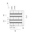
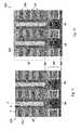
- FIGS. 1C-1Dare respectively side cross sectional and top cross sectional views of a NAND string of another embodiment.
- FIG. 1Cis a side cross sectional view of the device along line Y-Y′ in FIG. 1D
- FIG. 1Dis a side cross sectional view of the device along line X-X′ in FIG. 1C .
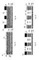
- FIGS. 6A-6Eare partial side cross-sectional views of a material layer stack that illustrate a method of forming control gate electrodes and a select line for a plurality of NAND memory strings.
- FIGS. 7A-7Jare partial side cross-sectional views of a material layer stack over a substrate that illustrate a method of fabricating NAND memory strings according to another embodiment.
- the embodiments of the inventionprovide a method for fabricating a semiconductor device, such as a three dimensional monolithic memory array comprising a plurality of NAND memory strings.
- a monolithic three dimensional memory arrayis one in which multiple memory levels are formed above a single substrate, such as a semiconductor wafer, with no intervening substrates.
- the term “monolithic”means that layers of each level of the array are directly deposited on the layers of each underlying level of the array.
- two dimensional arraysmay be formed separately and then packaged together to form a non-monolithic memory device.
- non-monolithic stacked memorieshave been constructed by forming memory levels on separate substrates and adhering the memory levels atop each other, as in Leedy, U.S. Pat. No. 5,915,167, titled “Three Dimensional Structure Memory.” The substrates may be thinned or removed from the memory levels before bonding, but as the memory levels are initially formed over separate substrates, such memories are not true monolithic three dimensional memory arrays.
- the first (e.g., source) electrode 102may connect to the bottom of the channel 1 and the second (e.g., drain electrode 103 ) may connect to the top of the channel 1 .
- the NAND string 150may further include drain-side and source-side select or access transistors (not shown in FIGS. 1A-2 for clarity) which may be located above and below the memory levels of the NAND string 150 , respectively.
- the semiconductor channel 1may be a filled feature, as shown in FIGS. 1C and 1D .
- the semiconductor channel 1may be hollow, for example a hollow cylinder filled with an insulating fill material 2 , as shown in FIGS. 1A and 1B .
- an insulating fill material 2may be formed to fill the hollow part surrounded by the semiconductor channel 1 .
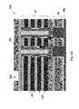
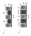
- a memory device 180may comprise a plurality of NAND strings 150 formed in a stack 120 of material layers over the substrate 100 , as shown in FIG. 2 .
- the substrate 100can be any semiconducting substrate known in the art, such as monocrystalline silicon, IV-IV compounds such as silicon-germanium or silicon-germanium-carbon, III-V compounds, II-VI compounds, epitaxial layers over such substrates, or any other semiconducting or non-semiconducting material, such as silicon oxide, glass, plastic, metal or ceramic substrate.
- the substrate 100may include integrated circuits fabricated thereon, such as driver circuits for a memory device.
- any suitable semiconductor materialscan be used for semiconductor channel 1 , for example silicon, germanium, silicon germanium, or other compound semiconductor materials, such as III-V, II-VI, or conductive or semiconductive oxides, etc.
- the semiconductor materialmay be amorphous, polycrystalline or single crystal.
- the semiconductor channel materialmay be formed by any suitable deposition methods.
- the semiconductor channel materialis deposited by low pressure chemical vapor deposition (LPCVD).
- LPCVDlow pressure chemical vapor deposition
- the semiconductor channel materialmay be a recyrstallized polycrystalline semiconductor material formed by recrystallizing an initially deposited amorphous semiconductor material.
- the insulating fill material 2may comprise any electrically insulating material, such as silicon oxide, silicon nitride, silicon oxynitride, or other high-k insulating materials.
- the monolithic three dimensional NAND strings 150further comprise a plurality of control gate electrodes 3 as shown in FIGS. 1A-2 .
- the control gate electrodes 3may comprise a portion having a strip shape extending substantially parallel to the major surface 100 a of the substrate 100 .
- the plurality of control gate electrodes 3comprise at least a first control gate electrode 3 a located in a first device level (e.g., memory device level A) and a second control gate electrode 3 b located in a second device level (e.g., memory device level B) located over the major surface 100 a of the substrate 100 and below the device level A.
- the control gate materialmay comprise any one or more suitable conductive or semiconductor control gate material known in the art, such as doped polysilicon, tungsten, tungsten nitride, copper, aluminum, tantalum, titanium, cobalt, titanium nitride, alloys thereof or combination of these materials.
- the control gate material in FIGS. 1A-1Dmay comprise a conductive metal or metal alloy, such as tungsten, titanium nitride, and/or tungsten nitride, while the control gate material in FIG. 2 may comprise doped polysilicon.
- a blocking dielectric 7is located adjacent to the control gate(s) 3 and may surround the control gate 3 , as shown in FIGS. 1A and 1C .
- a straight blocking dielectric layer 7may be located only adjacent to an edge (i e, minor surface) of each control gate 3 , as shown in FIG. 2 .
- the blocking dielectric 7may comprise one or more layers having plurality of blocking dielectric segments located in contact with a respective one of the plurality of control gate electrodes 3 .
- the blocking dielectric 7may comprise one or more continuous layers which extend the entire length of the memory cell portion of the NAND string 150 , as shown in FIG. 2 .
- the monolithic three dimensional NAND stringalso comprise a charge storage region 9 .
- the charge storage region 9may comprise one or more continuous layers which extend the entire length of the memory cell portion of the NAND string as shown in FIG. 2 .
- the charge storage region 9may comprise an insulating charge trapping material, such as a silicon nitride layer.
- the charge storage regionmay comprise a plurality of discrete charge storage regions or segments 9 located between the blocking dielectric 7 and the channel 1 , as shown in FIGS. 1A and 1C .
- the discrete charge storage regions 9may comprise a plurality of vertically spaced apart, conductive (e.g., metal such as tungsten, molybdenum, tantalum, titanium, platinum, ruthenium, and alloys thereof, or a metal silicide such as tungsten silicide, molybdenum silicide, tantalum silicide, titanium silicide, nickel silicide, cobalt silicide, or a combination thereof), or semiconductor (e.g., polysilicon) floating gates.
- the discrete charge storage regions 9may comprise an insulating charge trapping material, such as silicon nitride segments.
- the charge storage region 9may comprise conductive nanoparticles, such as metal nanoparticles, for example ruthenium nanoparticles.
- the tunnel dielectric 11 of the monolithic three dimensional NAND stringis located between charge storage region 9 and the semiconductor channel 1 .
- the blocking dielectric 7 and the tunnel dielectric 11may be independently selected from any one or more same or different electrically insulating materials, such as silicon oxide, silicon nitride, silicon oxynitride, or other insulating materials, such as metal oxide materials, for example aluminum oxide or hafnium oxide.
- the blocking dielectric 7 and/or the tunnel dielectric 11may include multiple layers of silicon oxide, silicon nitride and/or silicon oxynitride (e.g., ONO layers).
- the three-dimensional NAND string 150may have a generally pillar shape that extends substantially perpendicular to the major surface of the substrate 100 , with a first (e.g., drain) electrode 103 that connects to the NAND string 150 at the top of the NAND string 150 (i.e., distal to the substrate 100 ) and a second (e.g., source) electrode 102 that connects to the NAND string 150 at the bottom of the NAND string 150 (i.e., proximate to the substrate 100 ).
- a first (e.g., drain) electrode 103that connects to the NAND string 150 at the top of the NAND string 150 (i.e., distal to the substrate 100 )
- a second (e.g., source) electrode 102that connects to the NAND string 150 at the bottom of the NAND string 150 (i.e., proximate to the substrate 100 ).
- each NAND string 150may have a first select or access transistor (e.g., a drain-side select gate transistor) located above the memory levels of the NAND string 150 , and a second select or access transistor (e.g., a source-side select gate transistor) located below the memory levels of the NAND string 150 . Since the second or source-side select gate transistor is located below the memory levels of the NAND string 150 , forming effective contact between the semiconductor channel 1 of the NAND string 150 and the underlying select gate region of the device has proven challenging, particularly for high aspect ratio NAND strings 150 .
- a first select or access transistore.g., a drain-side select gate transistor
- a second select or access transistore.g., a source-side select gate transistor
- FIGS. 3A-3Iillustrate a method of making a memory device according to a first, non-limiting embodiment of the invention.
- the method of FIGS. 3A-3Imay result in a higher quality gate insulating layer 306 for the source side select gate transistor 301 .
- a select gate electrode 304may be formed over a first gate insulating layer 303 over a major surface 100 a of the substrate 100 .
- the select gate electrode 304is etched through a mask to form one or more openings 314 having vertically-extending sidewalls 315 , 316 and a horizontally-extending bottom surface 317 .
- a second gate insulating layer 306is formed on the sidewalls 315 , 316 of the openings, and a sacrificial spacer layer 319 is formed over the second gate insulating layer 306 on the sidewalls 315 , 316 of the opening 314 .
- the horizontal portions of the gate insulating layer 306are etched, such as by reactive ion etching, to expose the major surface of the substrate 100 under the gate insulating layer 306 , while the sacrificial spacer layer 319 protects the vertically-extending portions of the gate insulating layer 306 over the sidewalls of the openings.
- the sacrificial spacer layeris then removed from the sidewalls.
- the gate insulating layer 306is not subject to processing damage because it is protected by the sacrificial spacer layer 319 while the bottom surface of the opening 314 is etched to expose the surface of the semiconductor substrate 100 .
- the vertical portions of the gate insulating layer 306are not subjected to etching damage and may be higher quality than in prior art devices.
- FIG. 3Aillustrates a select gate portion 50 of a NAND string memory device according to one embodiment.
- a first gate insulating layer 303e.g., an oxide layer
- the first gate insulating layer 303may be formed by oxidation of the exposed surface of the semiconductor (e.g., silicon) substrate 100 . Any suitable oxidation process may be used, such as radical oxidation, dry oxidation, wet oxidation, etc to form a silicon oxide layer 303 .
- a layer 303 of insulating materialsuch as silicon oxide, may be deposited by chemical vapor deposition (“CVD”) or sputtering.
- the select gate electrode 304may comprise any suitable conductive material, such as a metal or metal alloy or doped semiconductor layer, and may be formed using any suitable process, such as via physical or chemical vapor deposition processes. In the embodiment of FIG.
- the select gate electrode 304includes a doped polysilicon layer 305 over the first gate insulating layer 303 , a metal nitride (e.g., tungsten nitride) liner layer 307 over the doped polysilicon layer 305 , and a metal (e.g., tungsten) layer 309 over the metal nitride liner layer 307 .
- An upper layer 311 of an insulating materiale.g., silicon nitride
- a mask layer 313is then formed over the upper layer 311 of insulating material. As shown in FIG. 3B , the mask layer 313 is patterned into a mask pattern defining open portions 312 in which layer 311 is exposed.
- the mask layer 313may comprise any suitable mask layer, such as photoresist or a hard mask material, such as amorphous carbon, silicon nitride, metal, etc., and may be patterned using photolithography.
- FIG. 3Cthe upper layer 311 of insulating material and the select gate electrode 304 are etched through the mask 313 to the first gate insulating layer 303 to form openings 314 corresponding to the locations of the open portions 312 in the mask 313 .
- the layers 311 , 304may be etched using reactive ion etching (RIE), for example.
- RIEreactive ion etching
- the select gate electrode 304may form at least a portion of the sidewalls 315 , 316 of each opening 314
- the first gate insulating layer 303may form the bottom surface 317 of each opening 314 .
- the mask layer 313may be removed, as shown in FIG. 3D .
- a second gate insulating layer 306may be formed over the upper layer 311 of insulating material and in the openings 314 over the sidewalls 315 , 316 and bottom surface 317 of each opening 314 , as shown in FIG. 3D .
- the second gate insulating layer 306may comprise an insulating material, such as silicon oxide, may be deposited using a suitable process such as by chemical vapor deposition (“CVD”) or sputtering.
- a sacrificial spacer layer 319may be formed over the second gate insulating layer 306 , including in the openings 314 over the sidewalls 315 , 316 and bottom surface 317 of each opening 314 , as shown in FIG. 3E .
- the sacrificial spacer layer 319may comprise an insulating material, such as silicon nitride, may be deposited using a suitable process such as by chemical vapor deposition (“CVD”) or sputtering.
- the sacrificial spacer layer 319 , the second gate insulating layer 306 and the first gate insulating layer 303may be etched on the bottom surface 317 of the openings 314 to expose the surface 100 a of the semiconductor substrate 100 .
- the layers 319 , 306 , 303may be etched using an anisotropic etching process, such as a sidewall spacer reactive ion etch, such that horizontally extending portions of the layers 319 , 306 , 303 , including the portions located over the bottom surfaces 317 of the openings 314 , are preferentially etched relative to vertically extending portions, such as the portions of the layers 319 , 306 , 303 located over the sidewalls 315 , 316 of the openings 314 .
- an anisotropic etching processsuch as a sidewall spacer reactive ion etch
- the sacrificial spacer layer 319may be completely etched from over the upper insulating layer 311 and the bottom surface 317 of the openings 314 , while at least a portion of the sacrificial spacer layer 319 may remain over the sidewalls 315 , 316 of the openings 314 , as shown in FIG. 3F .
- the vertically extending portions of the second gate insulating layer 306 over the sidewalls 315 , 316 of the openings 314may be protected from etching damage by the vertically extending portions (e.g., sidewall spacers 319 a ) of the sacrificial spacer layer 319 .
- the remaining sidewall spacers 319 a of the sacrificial spacer layer 319may then be removed to expose the second gate insulating layer 306 over the sidewalls 315 , 316 of the opening, as shown in FIG. 3G .
- the sacrificial spacer layer 319may be removed using any suitable process, such as by a selective wet etch.
- FIGS. 3H-3Iillustrate a method of forming protrusions 1 B comprising a semiconductor material within the openings 314 and contacting the surface 100 a of the semiconductor substrate 100 , in accordance with one non-limiting embodiment.
- an epitaxial single crystal semiconductor layersuch as a single crystal silicon layer 321 may be epitaxially grown on the exposed major surface 100 a of the substrate 100 over the bottom surfaces 317 of the openings 314 .
- FIG. 3Hillustrates the single crystal silicon layer 321 partially filling each of the openings 314 .
- the protrusions 1 Bmay be formed by forming at least one layer of a second material, such as a second semiconductor material (e.g., a polycrystalline semiconductor material, such as polysilicon), a metal and/or a metal nitride, over the epitaxial single crystal semiconductor layer 321 within each of the openings 314 .
- a second semiconductor materiale.g., a polycrystalline semiconductor material, such as polysilicon
- the protrusions 1 Bmay be formed by completely filling the openings 314 with the single crystal silicon layer 321 .
- the layer 321may optionally be planarized, such as by chemical mechanical polishing (CMP), to remove any portions of the layer 321 extending above the top of the openings 314 and to define a top surface 325 of the protrusions 1 B, which may be made planar with the top surface of the upper insulating layer 311 , as shown in FIG. 3I .
- CMPchemical mechanical polishing
- FIG. 3Iillustrates a portion of a completed lower (e.g., source) select gate device level 50 comprising lower (e.g. source) select gate transistors 301 for a NAND string memory device.
- the select gate device level 50includes a conductive select gate electrode 304 that extends generally parallel to the major surface 100 a of the substrate 100 and a plurality of protrusions 1 B that extend in a generally vertical direction from the major surface 100 a of the semiconductor substrate 100 and are located adjacent to the select gate electrode 304 .
- the protrusions 1 Bmay comprise a semiconductor material 321 and may form channel portions that extend generally perpendicular to the major surface 100 a of the substrate.
- the semiconductor channel portions 1 Bmay comprise pillar- or rail-shaped protrusions that extend in a generally vertical direction from the semiconductor substrate 100 , and may comprise epitaxial single crystal silicon, for example. Additional semiconductor channel portions 1 C may be located in the substrate 100 and may extend in a direction that is generally parallel to the major surface of the substrate 100 (e.g., to the left and right or into and out of the page in FIG. 3I ). The additional semiconductor channel portions 1 C may electrically couple the semiconductor channel portions of the protrusions 1 B to a conductive source line outside of the view of FIG. 3I .
- a first gate insulating layer 303may extend generally parallel to the major surface of the substrate 100 and may be located between the select gate electrode 304 and the substrate 100 .
- a second gate insulating layer 306may extend generally perpendicular to the major surface of the substrate 100 , and may be located between the select gate electrode 304 and first and second opposing side surfaces 323 , 324 of each of the protrusions 1 B.
- FIGS. 4A-4Iillustrate an alternative embodiment method of forming a lower (e.g., source) select gate device level 50 for a NAND string memory device.
- FIGS. 4A-4Dare identical to FIGS. 3A-D described above, and illustrate forming the first gate insulating layer 303 , the select gate electrode 304 and upper insulating layer 311 over the semiconductor substrate 100 ( FIG. 4A ), forming a patterned mask 313 with open portions 312 corresponding to the future locations of the openings 314 ( FIG. 4B ), etching the upper insulating layer 311 and the select gate electrode 304 through the mask 313 to the first gate insulating layer 303 to define the openings 314 ( FIG. 4C ), and forming a second gate insulating layer 306 over the upper insulating layer 306 and the openings 314 , including over the sidewalls 315 , 316 of the openings 314 ( FIG. 4D ).
- a sacrificial spacer layer 401is formed by depositing a material that preferentially forms over the second gate insulating layer 306 on the sidewalls 315 , 316 but not on the bottom surface 317 of the openings 314 .
- the sacrificial spacer layer 401 in this embodimentmay comprise carbon, and may be deposited by any suitable process, such as CVD.
- the selective formation of a carbon spacer layer 401 on the sidewalls 315 , 316 but not on the bottom surface 317may be promoted by controlling the parameters of the carbon deposition, such as the carbon deposition temperature, the thickness of the carbon layer 401 and the aspect ratio of the openings 314 .
- the deposition parametersmay otherwise be similar to non-conformal deposition processes
- the first and second gate insulating layers 303 , 306may then be etched on the bottom surface 317 of the openings 314 , such as via reactive ion etching, to expose the surface 100 a of the semiconductor substrate 100 , as shown in FIG. 4F .
- the sacrificial spacer layer 401may protect the vertically extending portions of the second gate insulating layer 306 over the sidewalls 315 , 315 of the openings 314 from etching damage.
- the sacrificial spacer layer 401may be removed, such as by ashing (e.g., when the layer 401 comprises carbon), as shown in FIG. 4F .
- a separate etching stepe.g., a wet chemical etch
- to remove the sacrificial spacer layer 319see FIG. 3G
- FIG. 4Gis identical to FIG. 3H and shows a single crystal silicon layer 321 epitaxially grown on the exposed major surface 100 a of the substrate 100 and partially filling each of the openings 314 . Unlike in the embodiment of FIGS. 3H-3I , however, the single crystal silicon layer 321 does not completely fill the openings 314 .
- a layer of a second materialwhich in this embodiment comprises doped or undoped polysilicon 403 , is formed over the single crystal silicon layer 321 and the upper insulating layer 311 , as shown in FIG. 4H .
- the polysilcon layer 403may be formed by plasma enhanced chemical vapor deposition (PECVD), for example.
- polysilicon 403 to partially fill the openings 314may result in lower cost than the use of only single crystal silicon 321 as shown in FIGS. 3H-3I .
- the growth rate of polysilicon 403 from epitaxial single crystal silicon 321 in the vertical directionmay be relatively high, which may promote selective formation of the polysilicon layer 403 over the single crystal silicon layer 321 within the openings 314 .
- a polycrystalline semiconductor (e.g., silicon) layermay be formed to fill the entire opening 314 and may then be recrystallized by thermal treatment or by laser annealing to form a single crystal semiconductor material.
- the polysilicon layer 403may be planarized, such as by an etch back or CMP, to remove portions of the layer 403 extending above the top of the openings 314 , such that the top of layer 403 is planar with the top of the upper insulating layer 311 , as shown in FIG. 4I .
- layer 403may be formed using selective epitaxial growth and the planarization step may be omitted.
- the concentration of HCl during polysilicon depositionmay be controlled such that the polysilicon layer 403 does not deposit on insulating layer 311 .
- FIG. 4Ishows the completed lower (e.g. source) select gate device level 50 , and is similar to FIG.
- the protrusions 1 Binclude a polysilicon layer 403 over a single crystal silicon layer 321 that contacts the semiconductor substrate 100 .
- the single crystal silicon layer 321may fill the entire openings 314 following use of the carbon mask 401 .
- a monolithic three-dimensional NAND string memory devicemay be fabricated by providing a stack 120 of alternating layers of a first material 19 and a second material 121 different from the first material 19 over a substrate 100 , and forming one or more memory openings 81 in the stack 120 that extend through the layers in a direction that is substantially perpendicular to the major surface of the substrate 100 .
- FIGS. 5A-5Jillustrate one method of forming NAND strings 150 in a stack 120 over a substrate 100 .
- the stack 120includes a lower (e.g., source) select gate device level 50 located below the future location of the memory device levels 70 as shown in FIG. 5A .
- the select gate device level 50may be formed as described above and shown in FIGS.
- select gate device level 50may be fabricated as described in U.S. patent application Ser. No. 14/133,979, filed on Dec. 19, 2013, which is incorporated by reference herein for all purposes.
- an etch stop layer 501may be formed over the select gate device level 50 , including over the top surfaces of the protrusions 1 B, as shown in FIG. 5A .
- the etch stop layer 501may comprise a material that has a relatively low etch rate using a first etch process (e.g., a reactive ion etch process). As described further below, the material of the etch stop layer 501 may have a relatively higher etch rate using a second etch process (e.g., a wet etching process).
- Suitable materials for the etch stop layer 501include intrinsic polysilicon, a nitride material (e.g., silicon nitride) and/or an oxide material (e.g., silicon oxide).
- the etch stop layer 501may be formed by depositing the layer 501 over the select gate device level 50 by any suitable deposition method, such as sputtering, CVD, PECVD, MBE, ALD, etc.
- the three dimensional memory device levels 70may be fabricated over the etch stop layer 501 by depositing a plurality of alternating layers 19 , 121 of a first material and a second material different than the first material as shown in FIG. 5A .
- Layers 19 , 121may be deposited over the etch stop layer 501 by any suitable deposition method, such as sputtering, CVD, PECVD, MBE, ALD, etc.
- the layers 19 , 121may be 6 to 100 nm thick.
- the first layers 19comprise an electrically insulating material. Any suitable insulating material may be used, such as silicon oxide, silicon nitride, silicon oxynitride, a high-k dielectric (e.g., aluminum oxide, hafnium oxide, etc. or an organic insulating material).
- the second layers 121comprise a sacrificial material, such an insulating material that is different from the material of the first layers 19 .
- layers 19may comprise silicon oxide and layers 121 may comprise silicon nitride.
- the deposition of layers 19 , 121is followed by etching the stack 120 to the etch stop layer 501 to form at least one front side opening 81 in the stack 120 .
- An array of a front side openings 81e.g., cylindrical memory openings or holes
- the openings 81may be formed by photolithography and etching, as follows. First, a memory hole mask 130 is formed over the stack and patterned to form openings 131 exposing the stack 120 , as shown in FIG. 5B .
- Mask 130may comprise any suitable material, such as one or more layer of photoresist and/or hard mask material. Then, the stack 120 may be etched (e.g., using reactive ion etching (RIE)) to form the openings 81 in the stack through the openings 131 in mask 130 , stopping the etch at the etch stop layer 501 .
- RIEreactive ion etching
- the etch stop layer 501may comprise a material (e.g., intrinsic polysilicon, a nitride or an oxide) having a low RIE etch rate (e.g., lower than the RIE etch rate for the materials of the alternating layers 19 , 121 of the stack 120 ).
- the layers 19 , 121may be more easily etched using RIE than the etch stop layer 501 .
- the etching process used to form the front side memory openings 81may be stopped at the etch stop layer 501 without exposing the surface of the protrusions 1 B in the openings 81 , as shown in FIG. 5C .
- Each of the front side openings 81may include a sidewall 505 that extends substantially perpendicular to the major surface of the substrate 100 and is defined by the exposed surfaces of the alternating layers 19 , 121 of the first insulating material and the second sacrificial material, and a bottom 507 defined by the etch stop layer 501 .
- the front side opening 81may include a first width dimension (e.g., a diameter), W 1 , at the bottom of the opening 81 proximate to the etch stop layer 501 , as shown in FIG. 5C .
- the etch stop layer 501may be etched through the bottom 507 of the front side openings 81 to expose the top surface 325 of the protrusion 1 B.
- the etch stop layer 501may be etched using a different etching process than the etching process (e.g., RIE) used to form the front side openings 81 .
- the etch stop layer 501is etched using a wet etch process.
- the etch stop layer 501may comprise a material having a high wet etch rate (e.g., higher than the wet etch rate of the materials of the alternating layers 19 , 121 of the stack and the upper surface of the protrusions 1 B).
- the etch stop layer 501may be more easily etched using a wet etch than the sidewall 505 and bottom surface 507 of the front side openings 81 .
- the etching of the etch stop layer 501 through the bottom 507 of the front side opening 81may provide a void area 509 between the bottom 507 of the opening 81 (indicated by dashed lines in FIG. 5D ) and the exposed top surface 325 of the protrusion 1 B.
- the void area 509may have a second width dimension, W 2 , that is larger than the first width dimension W 1 at the bottom 507 of the opening 81 .
- the void area 509 formed in the etch stop layer 501exposes a larger area of the top surface 325 of the protrusion 1 B than would be exposed if the front side opening 81 were extended to the top surface 325 of the protrusion 1 B (i.e., if the etch stop layer 501 were not present, and the front side memory opening 81 was formed by etching the stack 120 until the top surface 325 of the protrusion 1 B is reached at the bottom of the opening 81 ).
- a more effective electrical contactmay be made with the future channel 1 of the NAND string 150 formed in the opening 81 , as described in further detail below.
- FIGS. 5E-Jillustrate a method of forming the NAND memory strings 150 within the front side memory openings 81 .
- at least one memory film 7 , 9 , 11is formed in the memory openings 81 , including over the sidewalls 505 and bottom surfaces 325 of the memory openings 81 , and over the stack 120 .
- the at least one memory filmincludes one or more functional layers such as a blocking dielectric layer 7 , a charge storage layer 9 , and/or a tunneling dielectric layer 11 as described above in connection with FIGS. 1A-2 .
- the blocking dielectric layer 7may be formed over the sidewall 505 and bottom surface 325 of the memory opening 81 , the charge storage layer 9 may be formed over the blocking dielectric layer 7 , and the tunneling dielectric 11 may be formed over the charge storage layer 9 in the memory opening 81 .
- a cover layer 510is formed over the at least one memory film 7 , 9 , 11 in the memory openings 81 and over the stack 120 , as shown in FIG. 5E .
- a purpose of the cover layer 510is to protect the memory film 7 , 9 , 11 over the sidewall 505 of the memory opening 81 from damage during a subsequent etching step.
- the cover layer 510may be a semiconductor material, such as amorphous silicon or polysilicon.
- the at least one memory film 7 , 9 , 11 and the cover layer 510may each comprise a first portion 511 that extends over the sidewall 505 of the memory opening 81 in a direction that is substantially perpendicular to the major surface of the substrate 100 and a second portion 513 that is located in the void area 509 defined by the etch stop layer 501 and extends over the top surface 325 of the protrusion 1 B in a direction that is substantially parallel to the major surface of the substrate 100 .
- a first portion 511that extends over the sidewall 505 of the memory opening 81 in a direction that is substantially perpendicular to the major surface of the substrate 100
- a second portion 513that is located in the void area 509 defined by the etch stop layer 501 and extends over the top surface 325 of the protrusion 1 B in a direction that is substantially parallel to the major surface of the substrate 100 .
- each of the layers 7 , 9 , 11 , 510may have a first portion that 511 that extends generally vertically along the sidewall 505 of the memory opening 81 , and upon reaching the void area 509 each of the layers 7 , 9 , 11 , 510 may extend in a radially outward direction from the memory opening 81 into the void area 509 .
- Each of the layers 7 , 9 , 11 , 510may have a second portion 513 that continues in a generally horizontal direction over the top surface 325 of the protrusion 1 B.
- a mask layer 515may be formed over the cover layer 510 as shown in FIG. 5F .
- Mask layer 515may be a hard mask, such as an amorphous carbon layer for example, and may be deposited non-conformally such that the layer 515 is located over the cover layer 510 on the top of the stack 120 but does not extend into the memory openings 81 as shown in FIG. 5F .
- the layer 515may be deposited conformally and then patterned by photolithography and etching to be removed from the memory openings.
- portions of the at least one memory film 7 , 9 , 11 and the cover layer 510are removed in the horizontally-extending second portion 513 (see FIG. 5E ) to define a generally cylindrically-shaped connector region 517 that exposes the top surface 325 of the protrusion 1 B.
- the at least one memory film 7 , 9 , 11 and cover layer 510may be etched using RIE or another suitable anisotropic wet or dry etching method.
- the cover layer 510protects the memory film 7 , 9 , 11 along the sidewalls 505 of the memory openings 81 from etching damage and the mask layer 515 protects the rest of the stack 120 from being etched.
- the mask layer 515may be removed using any suitable method, such as ashing or selective wet etching. Alternatively, the mask layer 515 is omitted and a sidewall spacer anisotropic etch may be used to remove the horizontal portions of layers 7 , 9 , 11 and 510 while leaving the vertical portions of these layers in place as sidewall spacers. The anisotropic etch may be followed by a selective wet etch.
- a semiconductor channel material 519is formed in the memory openings 81 and within the connector region 517 such that it makes contact with the top surface 325 of the semiconductor channel protrusions 1 B.
- the semiconductor channel material 519comprises a channel material, such as amorphous silicon or polysilicon.
- the cover layer 510 and the semiconductor channel material 519preferably comprise the same materials, and layer 519 contacts layer 510 on the sidewalls 505 of the openings 81 . Together, layers 519 and 510 may form the semiconductor channel 1 as illustrated in FIGS. 1 A- 2 .
- the at least one memory film 7 , 9 , 11may be located between the semiconductor channel 1 and the sidewall 505 of the memory opening 81 .
- the semiconductor channel 1fills the connector region 517 to form a generally-cylindrically-shaped connector 521 that connects the semiconductor channel 1 to the top surface 325 of the protrusion 1 B.
- An optional core insulating layer 2such as a silicon oxide layer may be deposited in the openings 81 and over the stack 120 as shown in FIG. 5H . Layer 2 is also shown in FIGS. 1A and 1B .
- the stack 120may then be planarized as shown in FIG. 5I to remove layers 2 , 519 , 510 , 11 and 9 from the top of the stack 120 .
- the stack 120may be recessed by a dry etch process (e.g., RIE) to remove layers 2 , 519 , 510 , 11 and 9 from the top of the stack 120 as shown in FIG. 5I .
- the film of dielectric material 7may optionally be left over the top of the stack 120 .
- an insulating layer 523may be formed over the stack 120 , including over the memory openings 81 .
- the insulating layer 523may be a silicon oxide layer and may be formed by a suitable process (e.g., CVD) using a tetraethyl orthosilicate (TEOS) source.
- FIGS. 6A-6Eillustrate additional processing steps that may be performed to remove the layers of sacrificial material 121 from the stack 120 and form control gate electrodes 3 for a vertical NAND memory string 150 .
- a mask 601may be formed over the top of the stack 120 .
- the mask 601may be a photoresist and/or hard mask.
- At least one back side mask opening 603is formed in the mask.
- the stack 120is etched through the opening(s) 603 in the mask to form one or more back side openings (e.g., trenches) 605 in the stack 120 .
- the sacrificial second material layers 121may be removed through the back side openings 605 to form back side recesses 607 between the first material layers 19 , as shown in FIG. 6C .
- Layers 121may be removed by selective etching, such as a silicon nitride selective etching which removes silicon nitride layers 121 but does not remove the silicon oxide layers 19 .
- the selective etchmay stop on the oxide blocking dielectric 7 , such as a silicon oxide blocking dielectric, that extends vertically in the memory openings 81 .
- Electrically conductive control gate electrodes 3may then be formed in the back side recesses 607 through the back side opening 605 , as shown in FIG. 6D .
- the control gate electrode 3 materialmay comprise any suitable material described above with respect to FIGS. 1A-2 .
- the materialmay comprise a TiN liner and tungsten gate material.
- the electrodes 3may be formed by forming the electrically conductive control gate electrode material to partially or completely fill the back side opening 605 and to fill the back side recesses 607 such that the control gate electrode 3 material contacts the dielectric film 7 along the sidewalls of the memory openings 81 .
- the electrode materialmay then be removed from the back side opening 605 (e.g., using anisotropic etching) without removing the material forming the electrodes 3 .
- An optional doped source region 608may be implanted into channel region 1 C in the substrate 100 through the backside opening 605 .
- the source region 608may be doped opposite conductivity type (e.g., n-type) from the conductivity type (e.g., p-type) of the channel region 1 C.
- an insulating layer 609such as a silicon oxide or silicon nitride layer is formed on the sidewalls of the backside opening 605 such that the bottom surface of the backside opening 605 (e.g., the upper major surface of the semiconductor substrate 100 ) is exposed.
- a conductive source line 611e.g., a metal or metal nitride line, such as W, Ti, TiN, etc.
- W, Ti, TiN, etc.is then formed over the insulating layer 609 in the backside opening 605 such that the source line 611 contacts the source region 608 which in turn contacts the channel region 1 C in the substrate 100 .
- An upper (e.g., drain side) select gate electrode and transistormay also be formed above the memory levels 70 of each NAND string 150 .
- FIGS. 7I-7Jillustrate an alternative method of forming NAND strings 150 in a stack 120 over a substrate 100 .
- the stack 120 in FIG. 7I-7Jdiffers from the stack 120 in FIGS. 5A-5J and 6 A- 6 E in that instead of alternating layers of a first insulating (e.g., an oxide, such as silicon oxide) material 19 and a second sacrificial (e.g., a nitride, such as silicon nitride) material 121 , the stack 120 in FIGS.
- a first insulatinge.g., an oxide, such as silicon oxide
- a second sacrificiale.g., a nitride, such as silicon nitride
- the 7I-7Jincludes alternating layers of a first insulating (e.g., an oxide, such as silicon oxide) material and a second semiconductor (e.g., silicon, such as polysilicon) material 701 (e.g., an OPOP stack).
- a first insulating (e.g., an oxide, such as silicon oxide) materialand a second semiconductor (e.g., silicon, such as polysilicon) material 701 (e.g., an OPOP stack).
- the protrusion 1 B in the lower (e.g., source) select gate level 50includes an upper polysilicon layer 403 over a lower epitaxial single crystal silicon layer 321 that contacts the surface of the substrate 100 , such as shown in FIGS. 4A-4I .
- the method of FIGS. 7I-7Jis otherwise substantially identical to the method of FIGS. 5A-5J described above.
- the stack 120is etched through a mask 130 to an etch stop layer 501 located above the lower (e.g., source) select gate memory level 50 to form an array of front side memory openings 81 ( FIGS. 7B-7C ), and the etch stop layer 501 is etched through each of the memory openings 81 to provide a void area 509 between the bottom of the memory opening 81 and the surface of the upper polysilicon layer 403 of the protrusion 1 B ( FIG. 7D ). Then, at least one memory film 7 , 9 , 11 and a semiconductor cover layer 510 are formed over the sidewall 505 of the memory openings 81 and the top surface of the protrusion 1 B ( FIG.
- the at least one memory film 7 , 9 , 11 and the cover layer 510are etched to form a generally-cylindrical connector region 517 that exposes the top surface of the protrusion 1 B ( FIG. 7F ), and a semiconductor channel material 519 is formed in the memory opening 81 and the connector region 517 to provide a semiconductor channel 1 having a generally cylindrically-shaped connector 521 located within the connector region 517 and contacting the polysilicon upper layer 403 of the protrusion 1 B ( FIG. 7G ).
- the at least one memory film 7 , 9 , 11may be located between the semiconductor channel 1 and the sidewall 505 of the memory opening.
- An optional insulating fill material 2may be formed over the stack 120 and within the memory openings 81 ( FIGS. 7H-7I ) and an insulating layer 523 (e.g., an oxide layer formed using a TEOS source) may be provided over the stack ( FIG. 7J ).
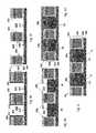
- FIGS. 8A-8Fillustrate yet another embodiment method of fabricating a NAND string memory device.
- FIG. 8Aillustrates a lower (e.g., source) select gate device level 50 and illustrates a plurality of openings 314 partially filled with an epitaxial single crystal silicon material 321 , as described above in FIGS. 3H and 4G .
- a semiconductor materiale.g., epitaxial single crystal silicon as shown in FIG. 3I , or epitaxial single crystal silicon and polysilcon as shown in FIG.
- the protrusions 1 Bare formed by forming at least one metal and/or metal nitride material layer over a semiconductor layer (e.g., epitaxial single crystal silicon layer 321 ) that contacts the semiconductor substrate 100 .
- a layer 801 of a metal or metal nitride materialmay be formed over the epitaxial silicon layer 321 as shown in FIG. 8B .
- the metal or metal nitride materialis preferably a refractive metal or metal alloy that may withstand a high temperature annealing process (e.g., laser annealing). Suitable materials include, without limitation, tungsten, tungsten nitride, tantalum, titanium, titanium nitride, and cobalt.
- a cap layer 803may be provided over the metal or metal nitride layer 801 , and may comprise a silicon oxide material formed by CVD using a silane (p-SiH 4 ) source.
- FIG. 8Cshows the lower (e.g., source) select gate device level 50 with protrusions 1 B comprising a semiconductor material 321 and an upper metal or metal nitride layer 801 with a cap layer 803 .
- a material layer stack 120 and etch stop layer 501are formed over the select gate device level 50 as described above in connection with FIGS. 5A and 7A .
- the stack 120may be processed to form front side memory openings 81 for a NAND string, as described above in connection with FIGS. 5A-E and 7 A- 7 E.
- FIG. 8Dcorresponds with FIGS. 5F and 7F described above, and shows the stack 120 with at least one memory film 7 , 9 , 11 and a cover layer 510 (e.g., a semiconductor channel material, such as polysilicon or amorphous silicon) formed over the sidewalls 505 of each of the memory openings 81 .
- a portion of the memory film 7 , 9 , 11 , cover layer 510 , and cap layer 803are removed (e.g., etched through a mask) from the bottom of the memory opening 81 to form a generally-cylindrical connector region 517 that exposes the surface of the metal or metal nitride layer 801 of the protrusion 1 B, as shown in FIG. 8D .
- a semiconductor channel material 519(e.g., polysilicon or amorphous silicon) may be formed in the memory opening 81 and in the connector region 517 to provide a semiconductor channel 1 having a generally cylindrically-shaped connector 521 located within the connector region 517 and contacting the exposed surface of the metal or metal nitride layer 801 of the protrusion 1 B, as shown in FIG. 8E .
- the at least one memory film 7 , 9 , 11may be located between the semiconductor channel 1 and the sidewall 505 of the memory opening 81 .
- An optional insulating fill material 2may be formed to fill the hollow part of the memory openings 81 surrounded by the semiconductor channel 1 .
- the devicemay be annealed, and in particular may be selectively annealed at elevated temperature to convert at least a portion of the material at the interface between the semiconductor channel 1 and the upper metal or metal nitride layer 801 of the protrusion 1 B to a metal silicide material 805 .
- the cylindrically-shaped connector 521may be reacted with the metal or metal nitride layer 801 to at least partially convert the connector 521 to a metal silicide material 805 .
- the metal silicide material 805may comprise, for example, WSi 2 , TaSi 2 , TiSiN, TiS 2 and CoSi 2 .
- the particular metal silicide material 805may depend on the material used for the upper metal or metal nitride layer 801 (e.g., a tungsten metal layer 801 forms a tungsten silicide layer 805 ).
- the selective annealing processmay comprise a laser anneal (e.g., directing a beam from a laser source through the oxide fill material 2 , which may be optically transmissive, to heat the cylindrically-shaped connector 521 at the interface between the semiconductor channel 1 and the metal layer 801 and convert at least a portion of the connector 521 to a metal silicide material 805 .
- the stack 120may also be planarized to the film of dielectric material 7 , and an insulating layer 523 may be formed over the stack 120 as shown in FIG. 8F .
Landscapes
- Semiconductor Memories (AREA)
- Non-Volatile Memory (AREA)
Abstract
Description
- This application claims the benefit of priority to U.S. Provisional Application No. 61/879,071, filed Sep. 17, 2013, the entire contents of which are incorporated by reference herein.
- The present invention relates generally to the field of semiconductor devices and specifically to three dimensional non-volatile memory, such as vertical NAND strings, and other three dimensional devices and methods of making thereof.
- Recently, ultra high density storage devices have been proposed using a three-dimensional (3D) stacked memory structure sometimes referred to as a Bit Cost Scalable (BiCS) architecture. For example, a 3D NAND stacked memory device can be formed from an array of alternating conductive and dielectric layers. A memory hole is formed through the layers to define many memory layers simultaneously. A NAND string is then formed by filling the memory hole with appropriate materials. A straight NAND string extends in one memory hole, while a pipe- or U-shaped NAND string (p-BiCS) includes a pair of vertical columns of memory cells
- Embodiments relate to a method of fabricating a memory device that includes forming a protrusion comprising a semiconductor material over a major surface of a semiconductor substrate, the protrusion having a top surface substantially parallel to the major surface of the substrate, forming an etch stop layer over the top surface of the protrusion, forming a stack of alternating layers of a first material and a second material different from the first material over the etch stop layer, etching the stack through a mask to the etch stop layer to form a memory opening having a first width dimension proximate to the etch stop layer, etching the etch stop layer to provide a void area between the top surface of the protrusion and a bottom of the memory opening, the void area having a second width dimension that is larger than the first width dimension, forming at least a portion of a memory film over a sidewall of the memory opening and within the void area over the top surface of the protrusion, etching the memory film to expose the top surface of the protrusion, and forming a semiconductor channel in the memory opening such that the semiconductor channel is electrically coupled to the protrusion and the at least a portion of the memory film is located between the semiconductor channel and the sidewall of the memory opening.
- Further embodiments relate to a memory device, such as a three-dimensional NAND string memory device, that includes a semiconductor substrate having a major surface, a protrusion comprising a semiconductor material over the major surface of the semiconductor substrate, the protrusion having a top surface substantially parallel to the major surface of the substrate, a first side surface and a second side surface opposite the first side surface, a select gate electrode extending over and parallel to the major surface of the semiconductor substrate and adjacent to the first and second side surfaces of the protrusion, and a gate insulating layer extending between the select gate electrode and the major surface of the substrate and between the select gate electrode and the first and second side surfaces of the protrusion. A stack of alternating insulating material layers and control gate electrodes are located over the substrate above the protrusion and the select gate electrode and includes a memory opening extending through the layer stack in a direction substantially perpendicular to the major surface of the substrate. A semiconductor channel having at least one first portion extends substantially perpendicular to the major surface of the substrate in the memory opening and at least one memory film is located in the memory opening adjacent to the semiconductor channel, wherein a first portion of the memory film is located between the control gate electrodes and the first portion of the semiconductor channel, and a second portion of the memory film extends over the top surface of the protrusion and defines a generally cylindrically-shaped connector region of the memory opening. A generally cylindrically-shaped connector is located within the connector region and electrically connects the protrusion to the semiconductor channel, wherein the memory opening above the connector region is wider than in the connector region.
FIGS. 1A-1B are respectively side cross sectional and top cross sectional views of a NAND string of one embodiment.FIG. 1A is a side cross sectional view of the device along line Y-Y′ inFIG. 1B , whileFIG. 1B is a side cross sectional view of the device along line X-X′ inFIG. 1A .FIGS. 1C-1D are respectively side cross sectional and top cross sectional views of a NAND string of another embodiment.FIG. 1C is a side cross sectional view of the device along line Y-Y′ inFIG. 1D , whileFIG. 1D is a side cross sectional view of the device along line X-X′ inFIG. 1C .FIG. 2 is a partial side cross-sectional view of a memory device comprising a plurality of NAND strings formed in a stack of material layers over a substrate.FIGS. 3A-3I are partial side cross-sectional views of a stack of material layers over a substrate and illustrate a method of forming a select gate level of a memory device according to an embodiment.FIGS. 4A-4I are partial side cross-sectional views of a stack of material layers over a substrate and illustrate a method of forming a select gate level of a memory device according to another embodiment.FIGS. 5A-5J are partial side cross-sectional views of a material layer stack over a substrate that illustrate a method of fabricating NAND memory strings according to one embodiment.FIGS. 6A-6E are partial side cross-sectional views of a material layer stack that illustrate a method of forming control gate electrodes and a select line for a plurality of NAND memory strings.FIGS. 7A-7J are partial side cross-sectional views of a material layer stack over a substrate that illustrate a method of fabricating NAND memory strings according to another embodiment.FIGS. 8A-8F are partial side cross-sectional views of a material layer stack that illustrate a method of forming a select gate level and a plurality of NAND strings with a metal silicide channel contact area according to an embodiment.- The embodiments of the invention provide a method for fabricating a semiconductor device, such as a three dimensional monolithic memory array comprising a plurality of NAND memory strings.
- A monolithic three dimensional memory array is one in which multiple memory levels are formed above a single substrate, such as a semiconductor wafer, with no intervening substrates. The term “monolithic” means that layers of each level of the array are directly deposited on the layers of each underlying level of the array. In contrast, two dimensional arrays may be formed separately and then packaged together to form a non-monolithic memory device. For example, non-monolithic stacked memories have been constructed by forming memory levels on separate substrates and adhering the memory levels atop each other, as in Leedy, U.S. Pat. No. 5,915,167, titled “Three Dimensional Structure Memory.” The substrates may be thinned or removed from the memory levels before bonding, but as the memory levels are initially formed over separate substrates, such memories are not true monolithic three dimensional memory arrays.
- In some embodiments, a monolithic three
dimensional NAND string 150 comprises asemiconductor channel 1 having at least one end portion extending substantially perpendicular to amajor surface 100aof asubstrate 100, as shown inFIGS. 1A ,1C and2. For example, thesemiconductor channel 1 may have a pillar shape extending through a plurality of memory device levels (Level A, Level B, etc.) and the entire pillar-shaped semiconductor channel in the memory device levels extends substantially perpendicularly to themajor surface 100aof thesubstrate 100, as shown inFIGS. 1A ,1C and2. Thechannels 1 may be electrically connected to first and second (e.g., source and drain)electrodes FIGS. 1A and 1C . The first (e.g., source)electrode 102 may connect to the bottom of thechannel 1 and the second (e.g., drain electrode103) may connect to the top of thechannel 1. TheNAND string 150 may further include drain-side and source-side select or access transistors (not shown inFIGS. 1A-2 for clarity) which may be located above and below the memory levels of theNAND string 150, respectively. - In some embodiments, the
semiconductor channel 1 may be a filled feature, as shown inFIGS. 1C and 1D . In some other embodiments, thesemiconductor channel 1 may be hollow, for example a hollow cylinder filled with aninsulating fill material 2, as shown inFIGS. 1A and 1B . In these embodiments, an insulatingfill material 2 may be formed to fill the hollow part surrounded by thesemiconductor channel 1. - A
memory device 180 may comprise a plurality of NAND strings150 formed in astack 120 of material layers over thesubstrate 100, as shown inFIG. 2 . Thesubstrate 100 can be any semiconducting substrate known in the art, such as monocrystalline silicon, IV-IV compounds such as silicon-germanium or silicon-germanium-carbon, III-V compounds, II-VI compounds, epitaxial layers over such substrates, or any other semiconducting or non-semiconducting material, such as silicon oxide, glass, plastic, metal or ceramic substrate. Thesubstrate 100 may include integrated circuits fabricated thereon, such as driver circuits for a memory device. - Any suitable semiconductor materials can be used for
semiconductor channel 1, for example silicon, germanium, silicon germanium, or other compound semiconductor materials, such as III-V, II-VI, or conductive or semiconductive oxides, etc. The semiconductor material may be amorphous, polycrystalline or single crystal. The semiconductor channel material may be formed by any suitable deposition methods. For example, in one embodiment, the semiconductor channel material is deposited by low pressure chemical vapor deposition (LPCVD). In some other embodiments, the semiconductor channel material may be a recyrstallized polycrystalline semiconductor material formed by recrystallizing an initially deposited amorphous semiconductor material. - The insulating
fill material 2 may comprise any electrically insulating material, such as silicon oxide, silicon nitride, silicon oxynitride, or other high-k insulating materials. - The monolithic three
dimensional NAND strings 150 further comprise a plurality ofcontrol gate electrodes 3 as shown inFIGS. 1A-2 . Thecontrol gate electrodes 3 may comprise a portion having a strip shape extending substantially parallel to themajor surface 100aof thesubstrate 100. The plurality ofcontrol gate electrodes 3 comprise at least a firstcontrol gate electrode 3alocated in a first device level (e.g., memory device level A) and a secondcontrol gate electrode 3blocated in a second device level (e.g., memory device level B) located over themajor surface 100aof thesubstrate 100 and below the device level A. The control gate material may comprise any one or more suitable conductive or semiconductor control gate material known in the art, such as doped polysilicon, tungsten, tungsten nitride, copper, aluminum, tantalum, titanium, cobalt, titanium nitride, alloys thereof or combination of these materials. For example, the control gate material inFIGS. 1A-1D may comprise a conductive metal or metal alloy, such as tungsten, titanium nitride, and/or tungsten nitride, while the control gate material inFIG. 2 may comprise doped polysilicon. - A blocking
dielectric 7 is located adjacent to the control gate(s)3 and may surround thecontrol gate 3, as shown inFIGS. 1A and 1C . Alternatively, a straightblocking dielectric layer 7 may be located only adjacent to an edge (i e, minor surface) of eachcontrol gate 3, as shown inFIG. 2 . The blockingdielectric 7 may comprise one or more layers having plurality of blocking dielectric segments located in contact with a respective one of the plurality ofcontrol gate electrodes 3. Alternatively, the blockingdielectric 7 may comprise one or more continuous layers which extend the entire length of the memory cell portion of theNAND string 150, as shown inFIG. 2 . - The monolithic three dimensional NAND string also comprise a
charge storage region 9. Thecharge storage region 9 may comprise one or more continuous layers which extend the entire length of the memory cell portion of the NAND string as shown inFIG. 2 . For example, thecharge storage region 9 may comprise an insulating charge trapping material, such as a silicon nitride layer. Alternatively, the charge storage region may comprise a plurality of discrete charge storage regions orsegments 9 located between the blockingdielectric 7 and thechannel 1, as shown inFIGS. 1A and 1C . The discretecharge storage regions 9 may comprise a plurality of vertically spaced apart, conductive (e.g., metal such as tungsten, molybdenum, tantalum, titanium, platinum, ruthenium, and alloys thereof, or a metal silicide such as tungsten silicide, molybdenum silicide, tantalum silicide, titanium silicide, nickel silicide, cobalt silicide, or a combination thereof), or semiconductor (e.g., polysilicon) floating gates. Alternatively, the discretecharge storage regions 9 may comprise an insulating charge trapping material, such as silicon nitride segments. Alternatively, thecharge storage region 9 may comprise conductive nanoparticles, such as metal nanoparticles, for example ruthenium nanoparticles. - The tunnel dielectric11 of the monolithic three dimensional NAND string is located between
charge storage region 9 and thesemiconductor channel 1. - The blocking
dielectric 7 and thetunnel dielectric 11 may be independently selected from any one or more same or different electrically insulating materials, such as silicon oxide, silicon nitride, silicon oxynitride, or other insulating materials, such as metal oxide materials, for example aluminum oxide or hafnium oxide. The blockingdielectric 7 and/or thetunnel dielectric 11 may include multiple layers of silicon oxide, silicon nitride and/or silicon oxynitride (e.g., ONO layers). - In various embodiments, the three-
dimensional NAND string 150 may have a generally pillar shape that extends substantially perpendicular to the major surface of thesubstrate 100, with a first (e.g., drain)electrode 103 that connects to theNAND string 150 at the top of the NAND string150 (i.e., distal to the substrate100) and a second (e.g., source)electrode 102 that connects to theNAND string 150 at the bottom of the NAND string150 (i.e., proximate to the substrate100). In embodiments, eachNAND string 150 may have a first select or access transistor (e.g., a drain-side select gate transistor) located above the memory levels of theNAND string 150, and a second select or access transistor (e.g., a source-side select gate transistor) located below the memory levels of theNAND string 150. Since the second or source-side select gate transistor is located below the memory levels of theNAND string 150, forming effective contact between thesemiconductor channel 1 of theNAND string 150 and the underlying select gate region of the device has proven challenging, particularly for high aspect ratio NAND strings150. - Various embodiments include methods of making a memory device such as a monolithic three-dimensional NAND string memory device.
FIGS. 3A-3I illustrate a method of making a memory device according to a first, non-limiting embodiment of the invention. The method ofFIGS. 3A-3I may result in a higher qualitygate insulating layer 306 for the source sideselect gate transistor 301. Specifically, aselect gate electrode 304 may be formed over a firstgate insulating layer 303 over amajor surface 100aof thesubstrate 100. Then, theselect gate electrode 304 is etched through a mask to form one ormore openings 314 having vertically-extendingsidewalls bottom surface 317. A secondgate insulating layer 306 is formed on thesidewalls sacrificial spacer layer 319 is formed over the secondgate insulating layer 306 on thesidewalls opening 314. Then, the horizontal portions of thegate insulating layer 306 are etched, such as by reactive ion etching, to expose the major surface of thesubstrate 100 under thegate insulating layer 306, while thesacrificial spacer layer 319 protects the vertically-extending portions of thegate insulating layer 306 over the sidewalls of the openings. The sacrificial spacer layer is then removed from the sidewalls. A protrusion comprising a semiconductor material, which later forms achannel portion 1B of theNAND string 150, is then formed in the opening, with thegate insulating layer 306 on thesidewalls opening 314 being located between theselect gate electrode 304 and the first and second side surfaces323,324 of the protrusion. Thegate insulating layer 306 is not subject to processing damage because it is protected by thesacrificial spacer layer 319 while the bottom surface of theopening 314 is etched to expose the surface of thesemiconductor substrate 100. Thus, the vertical portions of thegate insulating layer 306 are not subjected to etching damage and may be higher quality than in prior art devices. FIG. 3A illustrates aselect gate portion 50 of a NAND string memory device according to one embodiment. To form theselect gate portion 50 ofFIG. 3A , a first gate insulating layer303 (e.g., an oxide layer) may be formed over the surface of asemiconductor substrate 100. The firstgate insulating layer 303 may be formed by oxidation of the exposed surface of the semiconductor (e.g., silicon)substrate 100. Any suitable oxidation process may be used, such as radical oxidation, dry oxidation, wet oxidation, etc to form asilicon oxide layer 303. Alternatively, rather than oxidizing the exposed surface, alayer 303 of insulating material, such as silicon oxide, may be deposited by chemical vapor deposition (“CVD”) or sputtering.- One or
more layers gate insulating layer 303 to form theselect gate electrode 304. Theselect gate electrode 304 may comprise any suitable conductive material, such as a metal or metal alloy or doped semiconductor layer, and may be formed using any suitable process, such as via physical or chemical vapor deposition processes. In the embodiment ofFIG. 3A , theselect gate electrode 304 includes a dopedpolysilicon layer 305 over the firstgate insulating layer 303, a metal nitride (e.g., tungsten nitride)liner layer 307 over the dopedpolysilicon layer 305, and a metal (e.g., tungsten)layer 309 over the metalnitride liner layer 307. Anupper layer 311 of an insulating material (e.g., silicon nitride) may be provided over theselect gate electrode 304. - A
mask layer 313 is then formed over theupper layer 311 of insulating material. As shown inFIG. 3B , themask layer 313 is patterned into a mask pattern definingopen portions 312 in whichlayer 311 is exposed. Themask layer 313 may comprise any suitable mask layer, such as photoresist or a hard mask material, such as amorphous carbon, silicon nitride, metal, etc., and may be patterned using photolithography. InFIG. 3C , theupper layer 311 of insulating material and theselect gate electrode 304 are etched through themask 313 to the firstgate insulating layer 303 to formopenings 314 corresponding to the locations of theopen portions 312 in themask 313. Thelayers select gate electrode 304 may form at least a portion of thesidewalls opening 314, and the firstgate insulating layer 303 may form thebottom surface 317 of eachopening 314. Themask layer 313 may be removed, as shown inFIG. 3D . - A second
gate insulating layer 306 may be formed over theupper layer 311 of insulating material and in theopenings 314 over thesidewalls bottom surface 317 of eachopening 314, as shown inFIG. 3D . The secondgate insulating layer 306 may comprise an insulating material, such as silicon oxide, may be deposited using a suitable process such as by chemical vapor deposition (“CVD”) or sputtering. - A
sacrificial spacer layer 319 may be formed over the secondgate insulating layer 306, including in theopenings 314 over thesidewalls bottom surface 317 of eachopening 314, as shown inFIG. 3E . Thesacrificial spacer layer 319 may comprise an insulating material, such as silicon nitride, may be deposited using a suitable process such as by chemical vapor deposition (“CVD”) or sputtering. - In
FIG. 3F , thesacrificial spacer layer 319, the secondgate insulating layer 306 and the firstgate insulating layer 303 may be etched on thebottom surface 317 of theopenings 314 to expose thesurface 100aof thesemiconductor substrate 100. In embodiments, thelayers layers openings 314, are preferentially etched relative to vertically extending portions, such as the portions of thelayers sidewalls openings 314. During the etching, thesacrificial spacer layer 319 may be completely etched from over the upper insulatinglayer 311 and thebottom surface 317 of theopenings 314, while at least a portion of thesacrificial spacer layer 319 may remain over thesidewalls openings 314, as shown inFIG. 3F . Thus, the vertically extending portions of the secondgate insulating layer 306 over thesidewalls openings 314 may be protected from etching damage by the vertically extending portions (e.g.,sidewall spacers 319a) of thesacrificial spacer layer 319. - The remaining
sidewall spacers 319aof thesacrificial spacer layer 319 may then be removed to expose the secondgate insulating layer 306 over thesidewalls FIG. 3G . Thesacrificial spacer layer 319 may be removed using any suitable process, such as by a selective wet etch. FIGS. 3H-3I illustrate a method of formingprotrusions 1B comprising a semiconductor material within theopenings 314 and contacting thesurface 100aof thesemiconductor substrate 100, in accordance with one non-limiting embodiment. As shown inFIG. 3H , an epitaxial single crystal semiconductor layer, such as a singlecrystal silicon layer 321 may be epitaxially grown on the exposedmajor surface 100aof thesubstrate 100 over the bottom surfaces317 of theopenings 314.FIG. 3H illustrates the singlecrystal silicon layer 321 partially filling each of theopenings 314. In various embodiments described in further detail below, theprotrusions 1B may be formed by forming at least one layer of a second material, such as a second semiconductor material (e.g., a polycrystalline semiconductor material, such as polysilicon), a metal and/or a metal nitride, over the epitaxial singlecrystal semiconductor layer 321 within each of theopenings 314. In the embodiment shown inFIG. 3I , theprotrusions 1B may be formed by completely filling theopenings 314 with the singlecrystal silicon layer 321. Thelayer 321 may optionally be planarized, such as by chemical mechanical polishing (CMP), to remove any portions of thelayer 321 extending above the top of theopenings 314 and to define atop surface 325 of theprotrusions 1B, which may be made planar with the top surface of the upper insulatinglayer 311, as shown inFIG. 3I .FIG. 3I illustrates a portion of a completed lower (e.g., source) selectgate device level 50 comprising lower (e.g. source)select gate transistors 301 for a NAND string memory device. The selectgate device level 50 includes a conductiveselect gate electrode 304 that extends generally parallel to themajor surface 100aof thesubstrate 100 and a plurality ofprotrusions 1B that extend in a generally vertical direction from themajor surface 100aof thesemiconductor substrate 100 and are located adjacent to theselect gate electrode 304. Theprotrusions 1B may comprise asemiconductor material 321 and may form channel portions that extend generally perpendicular to themajor surface 100aof the substrate. Thesemiconductor channel portions 1B may comprise pillar- or rail-shaped protrusions that extend in a generally vertical direction from thesemiconductor substrate 100, and may comprise epitaxial single crystal silicon, for example. Additionalsemiconductor channel portions 1C may be located in thesubstrate 100 and may extend in a direction that is generally parallel to the major surface of the substrate100 (e.g., to the left and right or into and out of the page inFIG. 3I ). The additionalsemiconductor channel portions 1C may electrically couple the semiconductor channel portions of theprotrusions 1B to a conductive source line outside of the view ofFIG. 3I . A firstgate insulating layer 303 may extend generally parallel to the major surface of thesubstrate 100 and may be located between theselect gate electrode 304 and thesubstrate 100. A secondgate insulating layer 306 may extend generally perpendicular to the major surface of thesubstrate 100, and may be located between theselect gate electrode 304 and first and second opposing side surfaces323,324 of each of theprotrusions 1B.FIGS. 4A-4I illustrate an alternative embodiment method of forming a lower (e.g., source) selectgate device level 50 for a NAND string memory device.FIGS. 4A-4D are identical toFIGS. 3A-D described above, and illustrate forming the firstgate insulating layer 303, theselect gate electrode 304 and upper insulatinglayer 311 over the semiconductor substrate100 (FIG. 4A ), forming apatterned mask 313 withopen portions 312 corresponding to the future locations of the openings314 (FIG. 4B ), etching the upper insulatinglayer 311 and theselect gate electrode 304 through themask 313 to the firstgate insulating layer 303 to define the openings314 (FIG. 4C ), and forming a secondgate insulating layer 306 over the upper insulatinglayer 306 and theopenings 314, including over thesidewalls FIG. 4D ).- In
FIG. 4E , asacrificial spacer layer 401 is formed by depositing a material that preferentially forms over the secondgate insulating layer 306 on thesidewalls bottom surface 317 of theopenings 314. Thesacrificial spacer layer 401 in this embodiment may comprise carbon, and may be deposited by any suitable process, such as CVD. The selective formation of acarbon spacer layer 401 on thesidewalls bottom surface 317 may be promoted by controlling the parameters of the carbon deposition, such as the carbon deposition temperature, the thickness of thecarbon layer 401 and the aspect ratio of theopenings 314. The deposition parameters may otherwise be similar to non-conformal deposition processes - The first and second
gate insulating layers bottom surface 317 of theopenings 314, such as via reactive ion etching, to expose thesurface 100aof thesemiconductor substrate 100, as shown inFIG. 4F . During the etching, thesacrificial spacer layer 401 may protect the vertically extending portions of the secondgate insulating layer 306 over thesidewalls openings 314 from etching damage. Following the etching, thesacrificial spacer layer 401 may be removed, such as by ashing (e.g., when thelayer 401 comprises carbon), as shown inFIG. 4F . Thus, in this embodiment, a separate etching step (e.g., a wet chemical etch) to remove the sacrificial spacer layer319 (seeFIG. 3G ) may not be required. FIG. 4G is identical toFIG. 3H and shows a singlecrystal silicon layer 321 epitaxially grown on the exposedmajor surface 100aof thesubstrate 100 and partially filling each of theopenings 314. Unlike in the embodiment ofFIGS. 3H-3I , however, the singlecrystal silicon layer 321 does not completely fill theopenings 314. A layer of a second material, which in this embodiment comprises doped orundoped polysilicon 403, is formed over the singlecrystal silicon layer 321 and the upper insulatinglayer 311, as shown inFIG. 4H . Thepolysilcon layer 403 may be formed by plasma enhanced chemical vapor deposition (PECVD), for example. The use ofpolysilicon 403 to partially fill theopenings 314, as shown inFIGS. 4H-4I may result in lower cost than the use of onlysingle crystal silicon 321 as shown inFIGS. 3H-3I . Further, the growth rate ofpolysilicon 403 from epitaxialsingle crystal silicon 321 in the vertical direction may be relatively high, which may promote selective formation of thepolysilicon layer 403 over the singlecrystal silicon layer 321 within theopenings 314. Alternatively, a polycrystalline semiconductor (e.g., silicon) layer (doped or undoped) may be formed to fill theentire opening 314 and may then be recrystallized by thermal treatment or by laser annealing to form a single crystal semiconductor material.- The
polysilicon layer 403 may be planarized, such as by an etch back or CMP, to remove portions of thelayer 403 extending above the top of theopenings 314, such that the top oflayer 403 is planar with the top of the upper insulatinglayer 311, as shown inFIG. 4I . Alternatively,layer 403 may be formed using selective epitaxial growth and the planarization step may be omitted. For example, as described in U.S. Pat. No. 6,998,305, the concentration of HCl during polysilicon deposition may be controlled such that thepolysilicon layer 403 does not deposit on insulatinglayer 311.FIG. 4I shows the completed lower (e.g. source) selectgate device level 50, and is similar toFIG. 3I . In the embodiment ofFIG. 4I , theprotrusions 1B include apolysilicon layer 403 over a singlecrystal silicon layer 321 that contacts thesemiconductor substrate 100. Alternatively, the singlecrystal silicon layer 321 may fill theentire openings 314 following use of thecarbon mask 401. - A monolithic three-dimensional NAND string memory device may be fabricated by providing a
stack 120 of alternating layers of afirst material 19 and asecond material 121 different from thefirst material 19 over asubstrate 100, and forming one ormore memory openings 81 in thestack 120 that extend through the layers in a direction that is substantially perpendicular to the major surface of thesubstrate 100.FIGS. 5A-5J illustrate one method of formingNAND strings 150 in astack 120 over asubstrate 100. In this embodiment, thestack 120 includes a lower (e.g., source) selectgate device level 50 located below the future location of thememory device levels 70 as shown inFIG. 5A . The selectgate device level 50 may be formed as described above and shown inFIGS. 3A-3I and4A-4I. Other fabrication methods and/or selectgate device level 50 configurations may be used. For example, a lower selectgate device level 50 may be fabricated as described in U.S. patent application Ser. No. 14/133,979, filed on Dec. 19, 2013, which is incorporated by reference herein for all purposes. - In embodiments, an
etch stop layer 501 may be formed over the selectgate device level 50, including over the top surfaces of theprotrusions 1B, as shown inFIG. 5A . Theetch stop layer 501 may comprise a material that has a relatively low etch rate using a first etch process (e.g., a reactive ion etch process). As described further below, the material of theetch stop layer 501 may have a relatively higher etch rate using a second etch process (e.g., a wet etching process). Suitable materials for theetch stop layer 501 include intrinsic polysilicon, a nitride material (e.g., silicon nitride) and/or an oxide material (e.g., silicon oxide). Theetch stop layer 501 may be formed by depositing thelayer 501 over the selectgate device level 50 by any suitable deposition method, such as sputtering, CVD, PECVD, MBE, ALD, etc. - The three dimensional
memory device levels 70 may be fabricated over theetch stop layer 501 by depositing a plurality of alternatinglayers FIG. 5A .Layers etch stop layer 501 by any suitable deposition method, such as sputtering, CVD, PECVD, MBE, ALD, etc. Thelayers - In this embodiment, the
first layers 19 comprise an electrically insulating material. Any suitable insulating material may be used, such as silicon oxide, silicon nitride, silicon oxynitride, a high-k dielectric (e.g., aluminum oxide, hafnium oxide, etc. or an organic insulating material). Thesecond layers 121 comprise a sacrificial material, such an insulating material that is different from the material of the first layers19. For example, layers19 may comprise silicon oxide and layers121 may comprise silicon nitride. - The deposition of
layers stack 120 to theetch stop layer 501 to form at least onefront side opening 81 in thestack 120. An array of a front side openings81 (e.g., cylindrical memory openings or holes) may be formed in locations where vertical channels of NAND strings150 will be subsequently formed, as shown inFIGS. 5B and 5C . - The
openings 81 may be formed by photolithography and etching, as follows. First, amemory hole mask 130 is formed over the stack and patterned to formopenings 131 exposing thestack 120, as shown inFIG. 5B .Mask 130 may comprise any suitable material, such as one or more layer of photoresist and/or hard mask material. Then, thestack 120 may be etched (e.g., using reactive ion etching (RIE)) to form theopenings 81 in the stack through theopenings 131 inmask 130, stopping the etch at theetch stop layer 501. As discussed above, theetch stop layer 501 may comprise a material (e.g., intrinsic polysilicon, a nitride or an oxide) having a low RIE etch rate (e.g., lower than the RIE etch rate for the materials of the alternatinglayers layers etch stop layer 501. The etching process used to form the frontside memory openings 81 may be stopped at theetch stop layer 501 without exposing the surface of theprotrusions 1B in theopenings 81, as shown inFIG. 5C . - Each of the front side openings81 (e.g., cylindrical memory openings or holes) may include a
sidewall 505 that extends substantially perpendicular to the major surface of thesubstrate 100 and is defined by the exposed surfaces of the alternatinglayers etch stop layer 501. Thefront side opening 81 may include a first width dimension (e.g., a diameter), W1, at the bottom of theopening 81 proximate to theetch stop layer 501, as shown inFIG. 5C . - In
FIG. 5D , theetch stop layer 501 may be etched through thebottom 507 of thefront side openings 81 to expose thetop surface 325 of theprotrusion 1B. Theetch stop layer 501 may be etched using a different etching process than the etching process (e.g., RIE) used to form thefront side openings 81. In one embodiment, theetch stop layer 501 is etched using a wet etch process. Theetch stop layer 501 may comprise a material having a high wet etch rate (e.g., higher than the wet etch rate of the materials of the alternatinglayers protrusions 1B). Thus, theetch stop layer 501 may be more easily etched using a wet etch than thesidewall 505 andbottom surface 507 of thefront side openings 81. - The etching of the
etch stop layer 501 through thebottom 507 of thefront side opening 81 may provide avoid area 509 between the bottom507 of the opening81 (indicated by dashed lines inFIG. 5D ) and the exposedtop surface 325 of theprotrusion 1B. Thevoid area 509 may have a second width dimension, W2, that is larger than the first width dimension W1at the bottom507 of theopening 81. In other words, thevoid area 509 formed in theetch stop layer 501 exposes a larger area of thetop surface 325 of theprotrusion 1B than would be exposed if thefront side opening 81 were extended to thetop surface 325 of theprotrusion 1B (i.e., if theetch stop layer 501 were not present, and the frontside memory opening 81 was formed by etching thestack 120 until thetop surface 325 of theprotrusion 1B is reached at the bottom of the opening81). By exposing a larger surface area at thetop surface 325 of theprotrusion 1B, a more effective electrical contact may be made with thefuture channel 1 of theNAND string 150 formed in theopening 81, as described in further detail below. FIGS. 5E-J illustrate a method of forming theNAND memory strings 150 within the frontside memory openings 81. As shown inFIG. 5E , at least onememory film memory openings 81, including over thesidewalls 505 andbottom surfaces 325 of thememory openings 81, and over thestack 120. The at least one memory film includes one or more functional layers such as a blockingdielectric layer 7, acharge storage layer 9, and/or atunneling dielectric layer 11 as described above in connection withFIGS. 1A-2 . The blockingdielectric layer 7 may be formed over thesidewall 505 andbottom surface 325 of thememory opening 81, thecharge storage layer 9 may be formed over the blockingdielectric layer 7, and thetunneling dielectric 11 may be formed over thecharge storage layer 9 in thememory opening 81.- Then, a
cover layer 510 is formed over the at least onememory film memory openings 81 and over thestack 120, as shown inFIG. 5E . A purpose of thecover layer 510 is to protect thememory film sidewall 505 of the memory opening81 from damage during a subsequent etching step. Thecover layer 510 may be a semiconductor material, such as amorphous silicon or polysilicon. - As shown in
FIG. 5E , the at least onememory film cover layer 510 may each comprise afirst portion 511 that extends over thesidewall 505 of thememory opening 81 in a direction that is substantially perpendicular to the major surface of thesubstrate 100 and asecond portion 513 that is located in thevoid area 509 defined by theetch stop layer 501 and extends over thetop surface 325 of theprotrusion 1B in a direction that is substantially parallel to the major surface of thesubstrate 100. As shown inFIG. 5E , each of thelayers sidewall 505 of thememory opening 81, and upon reaching thevoid area 509 each of thelayers memory opening 81 into thevoid area 509. Each of thelayers second portion 513 that continues in a generally horizontal direction over thetop surface 325 of theprotrusion 1B. - A
mask layer 515 may be formed over thecover layer 510 as shown inFIG. 5F .Mask layer 515 may be a hard mask, such as an amorphous carbon layer for example, and may be deposited non-conformally such that thelayer 515 is located over thecover layer 510 on the top of thestack 120 but does not extend into thememory openings 81 as shown inFIG. 5F . Alternatively, thelayer 515 may be deposited conformally and then patterned by photolithography and etching to be removed from the memory openings. - As shown in
FIG. 5F , portions of the at least onememory film cover layer 510 are removed in the horizontally-extending second portion513 (seeFIG. 5E ) to define a generally cylindrically-shapedconnector region 517 that exposes thetop surface 325 of theprotrusion 1B. The at least onememory film cover layer 510 may be etched using RIE or another suitable anisotropic wet or dry etching method. Thecover layer 510 protects thememory film sidewalls 505 of thememory openings 81 from etching damage and themask layer 515 protects the rest of thestack 120 from being etched. Themask layer 515 may be removed using any suitable method, such as ashing or selective wet etching. Alternatively, themask layer 515 is omitted and a sidewall spacer anisotropic etch may be used to remove the horizontal portions oflayers - In
FIG. 5G , asemiconductor channel material 519 is formed in thememory openings 81 and within theconnector region 517 such that it makes contact with thetop surface 325 of thesemiconductor channel protrusions 1B. Thesemiconductor channel material 519 comprises a channel material, such as amorphous silicon or polysilicon. Thecover layer 510 and thesemiconductor channel material 519 preferably comprise the same materials, and layer519contacts layer 510 on thesidewalls 505 of theopenings 81. Together, layers519 and510 may form thesemiconductor channel 1 as illustrated in FIGS.1A-2. The at least onememory film semiconductor channel 1 and thesidewall 505 of thememory opening 81. Thesemiconductor channel 1 fills theconnector region 517 to form a generally-cylindrically-shapedconnector 521 that connects thesemiconductor channel 1 to thetop surface 325 of theprotrusion 1B. An optionalcore insulating layer 2, such as a silicon oxide layer may be deposited in theopenings 81 and over thestack 120 as shown inFIG. 5H .Layer 2 is also shown inFIGS. 1A and 1B . Thestack 120 may then be planarized as shown inFIG. 5I to removelayers stack 120. Alternately, thestack 120 may be recessed by a dry etch process (e.g., RIE) to removelayers stack 120 as shown inFIG. 5I . The film ofdielectric material 7 may optionally be left over the top of thestack 120. InFIG. 5J , an insulatinglayer 523 may be formed over thestack 120, including over thememory openings 81. The insulatinglayer 523 may be a silicon oxide layer and may be formed by a suitable process (e.g., CVD) using a tetraethyl orthosilicate (TEOS) source. FIGS. 6A-6E illustrate additional processing steps that may be performed to remove the layers ofsacrificial material 121 from thestack 120 and formcontrol gate electrodes 3 for a verticalNAND memory string 150. As shown inFIG. 6A , amask 601 may be formed over the top of thestack 120. Themask 601 may be a photoresist and/or hard mask. At least one backside mask opening 603 is formed in the mask. Then, as shown inFIG. 6B , thestack 120 is etched through the opening(s)603 in the mask to form one or more back side openings (e.g., trenches)605 in thestack 120.- Then, at least a portion of the sacrificial second material layers121 may be removed through the
back side openings 605 to form back side recesses607 between the first material layers19, as shown inFIG. 6C .Layers 121 may be removed by selective etching, such as a silicon nitride selective etching which removes silicon nitride layers121 but does not remove the silicon oxide layers19. The selective etch may stop on theoxide blocking dielectric 7, such as a silicon oxide blocking dielectric, that extends vertically in thememory openings 81. - Electrically conductive
control gate electrodes 3 may then be formed in the back side recesses607 through theback side opening 605, as shown inFIG. 6D . Thecontrol gate electrode 3 material may comprise any suitable material described above with respect toFIGS. 1A-2 . For example, the material may comprise a TiN liner and tungsten gate material. Theelectrodes 3 may be formed by forming the electrically conductive control gate electrode material to partially or completely fill theback side opening 605 and to fill the back side recesses607 such that thecontrol gate electrode 3 material contacts thedielectric film 7 along the sidewalls of thememory openings 81. The electrode material may then be removed from the back side opening605 (e.g., using anisotropic etching) without removing the material forming theelectrodes 3. An optionaldoped source region 608 may be implanted intochannel region 1C in thesubstrate 100 through thebackside opening 605. Thesource region 608 may be doped opposite conductivity type (e.g., n-type) from the conductivity type (e.g., p-type) of thechannel region 1C. - Then, as shown in
FIG. 6E , an insulatinglayer 609, such as a silicon oxide or silicon nitride layer is formed on the sidewalls of thebackside opening 605 such that the bottom surface of the backside opening605 (e.g., the upper major surface of the semiconductor substrate100) is exposed. A conductive source line611 (e.g., a metal or metal nitride line, such as W, Ti, TiN, etc.) is then formed over the insulatinglayer 609 in thebackside opening 605 such that thesource line 611 contacts thesource region 608 which in turn contacts thechannel region 1C in thesubstrate 100. This forms an electrical connection between the source line and thechannel portions memory levels 70 of eachNAND string 150. FIGS. 7I-7J illustrate an alternative method of formingNAND strings 150 in astack 120 over asubstrate 100. Thestack 120 inFIG. 7I-7J differs from thestack 120 inFIGS. 5A-5J and6A-6E in that instead of alternating layers of a first insulating (e.g., an oxide, such as silicon oxide)material 19 and a second sacrificial (e.g., a nitride, such as silicon nitride)material 121, thestack 120 inFIGS. 7I-7J includes alternating layers of a first insulating (e.g., an oxide, such as silicon oxide) material and a second semiconductor (e.g., silicon, such as polysilicon) material701 (e.g., an OPOP stack). In addition, as shown inFIG. 7A , theprotrusion 1B in the lower (e.g., source)select gate level 50 includes anupper polysilicon layer 403 over a lower epitaxial singlecrystal silicon layer 321 that contacts the surface of thesubstrate 100, such as shown inFIGS. 4A-4I . The method ofFIGS. 7I-7J is otherwise substantially identical to the method ofFIGS. 5A-5J described above. For example, thestack 120 is etched through amask 130 to anetch stop layer 501 located above the lower (e.g., source) selectgate memory level 50 to form an array of front side memory openings81 (FIGS. 7B-7C ), and theetch stop layer 501 is etched through each of thememory openings 81 to provide avoid area 509 between the bottom of thememory opening 81 and the surface of theupper polysilicon layer 403 of theprotrusion 1B (FIG. 7D ). Then, at least onememory film semiconductor cover layer 510 are formed over thesidewall 505 of thememory openings 81 and the top surface of theprotrusion 1B (FIG. 7E ), the at least onememory film cover layer 510 are etched to form a generally-cylindrical connector region 517 that exposes the top surface of theprotrusion 1B (FIG. 7F ), and asemiconductor channel material 519 is formed in thememory opening 81 and theconnector region 517 to provide asemiconductor channel 1 having a generally cylindrically-shapedconnector 521 located within theconnector region 517 and contacting the polysiliconupper layer 403 of theprotrusion 1B (FIG. 7G ). The at least onememory film semiconductor channel 1 and thesidewall 505 of the memory opening. An optional insulatingfill material 2 may be formed over thestack 120 and within the memory openings81 (FIGS. 7H-7I ) and an insulating layer523 (e.g., an oxide layer formed using a TEOS source) may be provided over the stack (FIG. 7J ).FIGS. 8A-8F illustrate yet another embodiment method of fabricating a NAND string memory device.FIG. 8A illustrates a lower (e.g., source) selectgate device level 50 and illustrates a plurality ofopenings 314 partially filled with an epitaxial singlecrystal silicon material 321, as described above inFIGS. 3H and 4G . In this embodiment, instead of completely filling theopenings 314 with a semiconductor material (e.g., epitaxial single crystal silicon as shown inFIG. 3I , or epitaxial single crystal silicon and polysilcon as shown inFIG. 4H-4I ), theprotrusions 1B are formed by forming at least one metal and/or metal nitride material layer over a semiconductor layer (e.g., epitaxial single crystal silicon layer321) that contacts thesemiconductor substrate 100. Alayer 801 of a metal or metal nitride material may be formed over theepitaxial silicon layer 321 as shown inFIG. 8B . The metal or metal nitride material is preferably a refractive metal or metal alloy that may withstand a high temperature annealing process (e.g., laser annealing). Suitable materials include, without limitation, tungsten, tungsten nitride, tantalum, titanium, titanium nitride, and cobalt. Acap layer 803 may be provided over the metal ormetal nitride layer 801, and may comprise a silicon oxide material formed by CVD using a silane (p-SiH4) source.FIG. 8C shows the lower (e.g., source) selectgate device level 50 withprotrusions 1B comprising asemiconductor material 321 and an upper metal ormetal nitride layer 801 with acap layer 803. Amaterial layer stack 120 andetch stop layer 501 are formed over the selectgate device level 50 as described above in connection withFIGS. 5A and 7A . Thestack 120 may be processed to form frontside memory openings 81 for a NAND string, as described above in connection withFIGS. 5A-E and7A-7E.FIG. 8D corresponds withFIGS. 5F and 7F described above, and shows thestack 120 with at least onememory film sidewalls 505 of each of thememory openings 81. A portion of thememory film cover layer 510, andcap layer 803 are removed (e.g., etched through a mask) from the bottom of thememory opening 81 to form a generally-cylindrical connector region 517 that exposes the surface of the metal ormetal nitride layer 801 of theprotrusion 1B, as shown inFIG. 8D .- A semiconductor channel material519 (e.g., polysilicon or amorphous silicon) may be formed in the
memory opening 81 and in theconnector region 517 to provide asemiconductor channel 1 having a generally cylindrically-shapedconnector 521 located within theconnector region 517 and contacting the exposed surface of the metal ormetal nitride layer 801 of theprotrusion 1B, as shown inFIG. 8E . The at least onememory film semiconductor channel 1 and thesidewall 505 of thememory opening 81. An optional insulatingfill material 2 may be formed to fill the hollow part of thememory openings 81 surrounded by thesemiconductor channel 1. - In
FIG. 8F , the device may be annealed, and in particular may be selectively annealed at elevated temperature to convert at least a portion of the material at the interface between thesemiconductor channel 1 and the upper metal ormetal nitride layer 801 of theprotrusion 1B to ametal silicide material 805. In embodiments, the cylindrically-shapedconnector 521 may be reacted with the metal ormetal nitride layer 801 to at least partially convert theconnector 521 to ametal silicide material 805. Themetal silicide material 805 may comprise, for example, WSi2, TaSi2, TiSiN, TiS2and CoSi2. The particularmetal silicide material 805 may depend on the material used for the upper metal or metal nitride layer801 (e.g., atungsten metal layer 801 forms a tungsten silicide layer805). The selective annealing process may comprise a laser anneal (e.g., directing a beam from a laser source through theoxide fill material 2, which may be optically transmissive, to heat the cylindrically-shapedconnector 521 at the interface between thesemiconductor channel 1 and themetal layer 801 and convert at least a portion of theconnector 521 to ametal silicide material 805. Thestack 120 may also be planarized to the film ofdielectric material 7, and an insulatinglayer 523 may be formed over thestack 120 as shown inFIG. 8F . - Although the foregoing refers to particular preferred embodiments, it will be understood that the invention is not so limited. It will occur to those of ordinary skill in the art that various modifications may be made to the disclosed embodiments and that such modifications are intended to be within the scope of the invention. All of the publications, patent applications and patents cited herein are incorporated herein by reference in their entirety.
Claims (26)
Priority Applications (2)
| Application Number | Priority Date | Filing Date | Title |
|---|---|---|---|
| US14/225,176US9460931B2 (en) | 2013-09-17 | 2014-03-25 | High aspect ratio memory hole channel contact formation |
| PCT/US2014/047480WO2015041743A1 (en) | 2013-09-17 | 2014-07-21 | High aspect ratio memory hole channel contact formation |
Applications Claiming Priority (2)
| Application Number | Priority Date | Filing Date | Title |
|---|---|---|---|
| US201361879071P | 2013-09-17 | 2013-09-17 | |
| US14/225,176US9460931B2 (en) | 2013-09-17 | 2014-03-25 | High aspect ratio memory hole channel contact formation |
Publications (2)
| Publication Number | Publication Date |
|---|---|
| US20150076584A1true US20150076584A1 (en) | 2015-03-19 |
| US9460931B2 US9460931B2 (en) | 2016-10-04 |
Family
ID=52667198
Family Applications (2)
| Application Number | Title | Priority Date | Filing Date |
|---|---|---|---|
| US14/225,116ActiveUS9023719B2 (en) | 2013-09-17 | 2014-03-25 | High aspect ratio memory hole channel contact formation |
| US14/225,176Active2034-08-27US9460931B2 (en) | 2013-09-17 | 2014-03-25 | High aspect ratio memory hole channel contact formation |
Family Applications Before (1)
| Application Number | Title | Priority Date | Filing Date |
|---|---|---|---|
| US14/225,116ActiveUS9023719B2 (en) | 2013-09-17 | 2014-03-25 | High aspect ratio memory hole channel contact formation |
Country Status (2)
| Country | Link |
|---|---|
| US (2) | US9023719B2 (en) |
| WO (1) | WO2015041743A1 (en) |
Cited By (71)
| Publication number | Priority date | Publication date | Assignee | Title |
|---|---|---|---|---|
| US20150348984A1 (en)* | 2014-05-30 | 2015-12-03 | SanDisk Technologies, Inc. | Method of making a monolithic three dimensional nand string using a select gate etch stop layer |
| US9236396B1 (en) | 2014-11-12 | 2016-01-12 | Sandisk Technologies Inc. | Three dimensional NAND device and method of making thereof |
| US9305849B1 (en) | 2014-11-12 | 2016-04-05 | Sandisk Technologies Inc. | Method of making a three dimensional NAND device |
| US9419012B1 (en) | 2015-06-19 | 2016-08-16 | Sandisk Technologies Llc | Three-dimensional memory structure employing air gap isolation |
| US9449987B1 (en) | 2015-08-21 | 2016-09-20 | Sandisk Technologies Llc | Three dimensional memory device with epitaxial semiconductor pedestal for peripheral transistors |
| US9515079B2 (en) | 2014-12-16 | 2016-12-06 | Sandisk Technologies Llc | Three dimensional memory device with blocking dielectric having enhanced protection against fluorine attack |
| CN106206507A (en)* | 2015-04-30 | 2016-12-07 | 旺宏电子股份有限公司 | Semiconductor structure and manufacturing method thereof |
| US9530785B1 (en) | 2015-07-21 | 2016-12-27 | Sandisk Technologies Llc | Three-dimensional memory devices having a single layer channel and methods of making thereof |
| US9589981B2 (en) | 2015-06-15 | 2017-03-07 | Sandisk Technologies Llc | Passive devices for integration with three-dimensional memory devices |
| US9595535B1 (en) | 2016-02-18 | 2017-03-14 | Sandisk Technologies Llc | Integration of word line switches with word line contact via structures |
| KR20170030357A (en)* | 2015-09-09 | 2017-03-17 | 삼성전자주식회사 | Semiconductor devices and methods of manufacturing the same |
| US9601502B2 (en) | 2014-08-26 | 2017-03-21 | Sandisk Technologies Llc | Multiheight contact via structures for a multilevel interconnect structure |
| US9601508B2 (en) | 2015-04-27 | 2017-03-21 | Sandisk Technologies Llc | Blocking oxide in memory opening integration scheme for three-dimensional memory structure |
| US9613977B2 (en) | 2015-06-24 | 2017-04-04 | Sandisk Technologies Llc | Differential etch of metal oxide blocking dielectric layer for three-dimensional memory devices |
| US9620512B1 (en) | 2015-10-28 | 2017-04-11 | Sandisk Technologies Llc | Field effect transistor with a multilevel gate electrode for integration with a multilevel memory device |
| US9620514B2 (en) | 2014-09-05 | 2017-04-11 | Sandisk Technologies Llc | 3D semicircular vertical NAND string with self aligned floating gate or charge trap cell memory cells and methods of fabricating and operating the same |
| US9627399B2 (en) | 2015-07-24 | 2017-04-18 | Sandisk Technologies Llc | Three-dimensional memory device with metal and silicide control gates |
| US9646981B2 (en) | 2015-06-15 | 2017-05-09 | Sandisk Technologies Llc | Passive devices for integration with three-dimensional memory devices |
| US9659866B1 (en) | 2016-07-08 | 2017-05-23 | Sandisk Technologies Llc | Three-dimensional memory structures with low source line resistance |
| US9659955B1 (en) | 2015-10-28 | 2017-05-23 | Sandisk Technologies Llc | Crystalinity-dependent aluminum oxide etching for self-aligned blocking dielectric in a memory structure |
| US9673213B1 (en) | 2016-02-15 | 2017-06-06 | Sandisk Technologies Llc | Three dimensional memory device with peripheral devices under dummy dielectric layer stack and method of making thereof |
| US9691778B2 (en) | 2014-08-26 | 2017-06-27 | Sandisk Technologies Llc | Multiheight contact via structures for a multilevel interconnect structure |
| US9698152B2 (en) | 2014-11-13 | 2017-07-04 | Sandisk Technologies Llc | Three-dimensional memory structure with multi-component contact via structure and method of making thereof |
| US9716062B2 (en) | 2015-02-05 | 2017-07-25 | Sandisk Technologies Llc | Multilevel interconnect structure and methods of manufacturing the same |
| US9716105B1 (en) | 2016-08-02 | 2017-07-25 | Sandisk Technologies Llc | Three-dimensional memory device with different thickness insulating layers and method of making thereof |
| US9721663B1 (en) | 2016-02-18 | 2017-08-01 | Sandisk Technologies Llc | Word line decoder circuitry under a three-dimensional memory array |
| US9728547B1 (en) | 2016-05-19 | 2017-08-08 | Sandisk Technologies Llc | Three-dimensional memory device with aluminum-containing etch stop layer for backside contact structure and method of making thereof |
| US9748266B1 (en) | 2016-07-20 | 2017-08-29 | Sandisk Technologies Llc | Three-dimensional memory device with select transistor having charge trapping gate dielectric layer and methods of making and operating thereof |
| US9754820B2 (en) | 2016-02-01 | 2017-09-05 | Sandisk Technologies Llc | Three-dimensional memory device containing an aluminum oxide etch stop layer for backside contact structure and method of making thereof |
| US20170263623A1 (en)* | 2015-08-31 | 2017-09-14 | Cypress Semiconductor Corporation | Memory Device with Multi-Layer Channel and Charge Trapping Layer |
| WO2017172389A1 (en)* | 2016-04-01 | 2017-10-05 | Micron Technology, Inc. | Thermal insulation for three-dimensional memory arrays |
| US9799669B2 (en) | 2013-09-15 | 2017-10-24 | Sandisk Technologies Llc | Single-semiconductor-layer channel in a memory opening for a three-dimensional non-volatile memory device |
| US9812463B2 (en) | 2016-03-25 | 2017-11-07 | Sandisk Technologies Llc | Three-dimensional memory device containing vertically isolated charge storage regions and method of making thereof |
| US9837431B2 (en) | 2015-11-20 | 2017-12-05 | Sandisk Technologies Llc | 3D semicircular vertical NAND string with recessed inactive semiconductor channel sections |
| US20170352669A1 (en)* | 2015-02-04 | 2017-12-07 | Sandisk Technologies Llc | Three-dimensional memory device having multilayer word lines containing selectively grown cobalt or ruthenium and method of making the same |
| US20180006050A1 (en)* | 2015-06-04 | 2018-01-04 | Toshiba Memory Corporation | Semiconductor memory device and method for manufacturing same |
| US9876031B1 (en) | 2016-11-30 | 2018-01-23 | Sandisk Technologies Llc | Three-dimensional memory device having passive devices at a buried source line level and method of making thereof |
| US9899399B2 (en) | 2015-10-30 | 2018-02-20 | Sandisk Technologies Llc | 3D NAND device with five-folded memory stack structure configuration |
| US9929174B1 (en) | 2016-10-28 | 2018-03-27 | Sandisk Technologies Llc | Three-dimensional memory device having non-uniform spacing among memory stack structures and method of making thereof |
| US9935124B2 (en) | 2015-11-25 | 2018-04-03 | Sandisk Technologies Llc | Split memory cells with unsplit select gates in a three-dimensional memory device |
| US9960180B1 (en) | 2017-03-27 | 2018-05-01 | Sandisk Technologies Llc | Three-dimensional memory device with partially discrete charge storage regions and method of making thereof |
| US9978768B2 (en) | 2016-06-29 | 2018-05-22 | Sandisk Technologies Llc | Method of making three-dimensional semiconductor memory device having laterally undulating memory films |
| US9984963B2 (en) | 2015-02-04 | 2018-05-29 | Sandisk Technologies Llc | Cobalt-containing conductive layers for control gate electrodes in a memory structure |
| US9985046B2 (en) | 2016-06-13 | 2018-05-29 | Sandisk Technologies Llc | Method of forming a staircase in a semiconductor device using a linear alignment control feature |
| US9991277B1 (en) | 2016-11-28 | 2018-06-05 | Sandisk Technologies Llc | Three-dimensional memory device with discrete self-aligned charge storage elements and method of making thereof |
| US20180211970A1 (en)* | 2016-11-17 | 2018-07-26 | Sandisk Technologies Llc | Three-dimensional memory device with self-aligned drain side select gate electrodes and method of making thereof |
| US10050054B2 (en) | 2016-10-05 | 2018-08-14 | Sandisk Technologies Llc | Three-dimensional memory device having drain select level isolation structure and method of making thereof |
| US10121794B2 (en) | 2016-06-20 | 2018-11-06 | Sandisk Technologies Llc | Three-dimensional memory device having epitaxial germanium-containing vertical channel and method of making thereof |
| US10224104B2 (en) | 2016-03-23 | 2019-03-05 | Sandisk Technologies Llc | Three dimensional NAND memory device with common bit line for multiple NAND strings in each memory block |
| US10355015B2 (en) | 2016-03-23 | 2019-07-16 | Sandisk Technologies Llc | Three-dimensional NAND memory device with common bit line for multiple NAND strings in each memory block |
| US10373969B2 (en) | 2018-01-09 | 2019-08-06 | Sandisk Technologies Llc | Three-dimensional memory device including partially surrounding select gates and fringe field assisted programming thereof |
| US10438964B2 (en) | 2017-06-26 | 2019-10-08 | Sandisk Technologies Llc | Three-dimensional memory device having direct source contact and metal oxide blocking dielectric and method of making thereof |
| US10453798B2 (en) | 2017-09-27 | 2019-10-22 | Sandisk Technologies Llc | Three-dimensional memory device with gated contact via structures and method of making thereof |
| US10453854B2 (en) | 2017-11-15 | 2019-10-22 | Sandisk Technologies Llc | Three-dimensional memory device with thickened word lines in terrace region |
| US10461163B2 (en) | 2017-11-15 | 2019-10-29 | Sandisk Technologies Llc | Three-dimensional memory device with thickened word lines in terrace region and method of making thereof |
| US20190371661A1 (en)* | 2016-09-21 | 2019-12-05 | SK Hynix Inc. | Semiconductor device and manufacturing method thereof |
| CN110931500A (en)* | 2019-10-25 | 2020-03-27 | 长江存储科技有限责任公司 | 3D memory device and method of manufacturing the same |
| CN110943091A (en)* | 2019-12-11 | 2020-03-31 | 长江存储科技有限责任公司 | Manufacturing method of three-dimensional memory |
| US10622368B2 (en) | 2015-06-24 | 2020-04-14 | Sandisk Technologies Llc | Three-dimensional memory device with semicircular metal-semiconductor alloy floating gate electrodes and methods of making thereof |
| US20200168625A1 (en)* | 2018-11-22 | 2020-05-28 | Yangtze Memory Technologies Co., Ltd. | Three-dimensional memory devices and fabrication methods thereof |
| US10756186B2 (en) | 2018-04-12 | 2020-08-25 | Sandisk Technologies Llc | Three-dimensional memory device including germanium-containing vertical channels and method of making the same |
| CN112071852A (en)* | 2020-08-12 | 2020-12-11 | 长江存储科技有限责任公司 | Three-dimensional memory structure and preparation method thereof |
| US10903226B2 (en)* | 2013-11-08 | 2021-01-26 | Samsung Electronics Co., Ltd. | Semiconductor device |
| CN112768453A (en)* | 2018-04-19 | 2021-05-07 | 长江存储科技有限责任公司 | Memory device and forming method thereof |
| US11047847B2 (en)* | 2015-10-02 | 2021-06-29 | Wake Forest University Health Sciences | Methods and apparatus for modeling cancer metastasis in vitro |
| JP2022528733A (en)* | 2019-04-12 | 2022-06-15 | 長江存儲科技有限責任公司 | Three-dimensional memory device on which semiconductor plugs are deposited and its formation method |
| TWI773086B (en)* | 2020-11-17 | 2022-08-01 | 大陸商長江存儲科技有限責任公司 | Method for forming three-dimensional memory device |
| US11469243B2 (en)* | 2019-10-22 | 2022-10-11 | Yangtze Memory Technologies Co., Ltd. | Three-dimensional memory device having pocket structure in memory string and method for forming the same |
| US11488977B2 (en) | 2020-04-14 | 2022-11-01 | Yangtze Memory Technologies Co., Ltd. | Three-dimensional memory devices and methods for forming the same |
| US20230137340A1 (en)* | 2021-10-29 | 2023-05-04 | Samsung Electronics Co., Ltd. | Pattern formation method and semiconductor device fabrication method using the same |
| US12038432B2 (en) | 2018-02-02 | 2024-07-16 | Wake Forest University Health Sciences | Organoids related to immunotherapy and methods of preparing and using the same |
Families Citing this family (86)
| Publication number | Priority date | Publication date | Assignee | Title |
|---|---|---|---|---|
| US8921891B2 (en)* | 2012-08-22 | 2014-12-30 | Micron Technology, Inc. | Vertical memory cell string with dielectric in a portion of the body |
| US9230987B2 (en) | 2014-02-20 | 2016-01-05 | Sandisk Technologies Inc. | Multilevel memory stack structure and methods of manufacturing the same |
| US9023719B2 (en)* | 2013-09-17 | 2015-05-05 | Sandisk Technologies Inc. | High aspect ratio memory hole channel contact formation |
| US9425237B2 (en) | 2014-03-11 | 2016-08-23 | Crossbar, Inc. | Selector device for two-terminal memory |
| US9768234B2 (en)* | 2014-05-20 | 2017-09-19 | Crossbar, Inc. | Resistive memory architecture and devices |
| US20150371925A1 (en)* | 2014-06-20 | 2015-12-24 | Intel Corporation | Through array routing for non-volatile memory |
| US9379124B2 (en)* | 2014-06-25 | 2016-06-28 | Sandisk Technologies Inc. | Vertical floating gate NAND with selectively deposited ALD metal films |
| US10211397B1 (en) | 2014-07-07 | 2019-02-19 | Crossbar, Inc. | Threshold voltage tuning for a volatile selection device |
| US9633724B2 (en) | 2014-07-07 | 2017-04-25 | Crossbar, Inc. | Sensing a non-volatile memory device utilizing selector device holding characteristics |
| US9460788B2 (en) | 2014-07-09 | 2016-10-04 | Crossbar, Inc. | Non-volatile memory cell utilizing volatile switching two terminal device and a MOS transistor |
| US10115819B2 (en) | 2015-05-29 | 2018-10-30 | Crossbar, Inc. | Recessed high voltage metal oxide semiconductor transistor for RRAM cell |
| US9698201B2 (en) | 2014-07-09 | 2017-07-04 | Crossbar, Inc. | High density selector-based non volatile memory cell and fabrication |
| US9685483B2 (en) | 2014-07-09 | 2017-06-20 | Crossbar, Inc. | Selector-based non-volatile cell fabrication utilizing IC-foundry compatible process |
| US9666594B2 (en) | 2014-09-05 | 2017-05-30 | Sandisk Technologies Llc | Multi-charge region memory cells for a vertical NAND device |
| US9780102B2 (en)* | 2014-11-07 | 2017-10-03 | Micron Technology, Inc. | Memory cell pillar including source junction plug |
| US9576971B2 (en) | 2014-12-09 | 2017-02-21 | Sandisk Technologies Llc | Three-dimensional memory structure having a back gate electrode |
| US9627403B2 (en) | 2015-04-30 | 2017-04-18 | Sandisk Technologies Llc | Multilevel memory stack structure employing support pillar structures |
| KR102282139B1 (en)* | 2015-05-12 | 2021-07-28 | 삼성전자주식회사 | Semiconductor devices |
| US9548121B2 (en)* | 2015-06-18 | 2017-01-17 | Macronix International Co., Ltd. | Memory device having only the top poly cut |
| US9502471B1 (en) | 2015-08-25 | 2016-11-22 | Sandisk Technologies Llc | Multi tier three-dimensional memory devices including vertically shared bit lines |
| KR102472561B1 (en) | 2015-10-01 | 2022-12-01 | 삼성전자주식회사 | Semiconductor memory device |
| US9397111B1 (en)* | 2015-10-30 | 2016-07-19 | Sandisk Technologies Llc | Select gate transistor with single crystal silicon for three-dimensional memory |
| US9754958B2 (en) | 2015-10-30 | 2017-09-05 | Sandisk Technologies Llc | Three-dimensional memory devices having a shaped epitaxial channel portion and method of making thereof |
| US9842851B2 (en) | 2015-10-30 | 2017-12-12 | Sandisk Technologies Llc | Three-dimensional memory devices having a shaped epitaxial channel portion |
| US9659956B1 (en) | 2016-01-06 | 2017-05-23 | Sandisk Technologies Llc | Three-dimensional memory device containing source select gate electrodes with enhanced electrical isolation |
| KR102624498B1 (en) | 2016-01-28 | 2024-01-12 | 삼성전자주식회사 | Vertical memory devices and methods of manufacturing the same |
| US10355139B2 (en) | 2016-06-28 | 2019-07-16 | Sandisk Technologies Llc | Three-dimensional memory device with amorphous barrier layer and method of making thereof |
| US10361213B2 (en) | 2016-06-28 | 2019-07-23 | Sandisk Technologies Llc | Three dimensional memory device containing multilayer wordline barrier films and method of making thereof |
| US9576967B1 (en) | 2016-06-30 | 2017-02-21 | Sandisk Technologies Llc | Method of suppressing epitaxial growth in support openings and three-dimensional memory device containing non-epitaxial support pillars in the support openings |
| US10529620B2 (en) | 2016-07-13 | 2020-01-07 | Sandisk Technologies Llc | Three-dimensional memory device containing word lines formed by selective tungsten growth on nucleation controlling surfaces and methods of manufacturing the same |
| US10381372B2 (en) | 2016-07-13 | 2019-08-13 | Sandisk Technologies Llc | Selective tungsten growth for word lines of a three-dimensional memory device |
| JP6759004B2 (en)* | 2016-08-29 | 2020-09-23 | 東京エレクトロン株式会社 | How to process the object to be processed |
| US10014316B2 (en) | 2016-10-18 | 2018-07-03 | Sandisk Technologies Llc | Three-dimensional memory device with leakage reducing support pillar structures and method of making thereof |
| US9881929B1 (en) | 2016-10-27 | 2018-01-30 | Sandisk Technologies Llc | Multi-tier memory stack structure containing non-overlapping support pillar structures and method of making thereof |
| US9978766B1 (en) | 2016-11-09 | 2018-05-22 | Sandisk Technologies Llc | Three-dimensional memory device with electrically isolated support pillar structures and method of making thereof |
| US9972641B1 (en) | 2016-11-17 | 2018-05-15 | Sandisk Technologies Llc | Three-dimensional memory device having a multilevel drain select gate electrode and method of making thereof |
| US10083982B2 (en) | 2016-11-17 | 2018-09-25 | Sandisk Technologies Llc | Three-dimensional memory device having select gate electrode that is thicker than word lines and method of making thereof |
| US9899410B1 (en)* | 2016-12-13 | 2018-02-20 | Sandisk Technologies Llc | Charge storage region in non-volatile memory |
| US10074666B2 (en) | 2017-01-09 | 2018-09-11 | Sandisk Technologies Llc | Three-dimensional memory device with enhanced mechanical stability semiconductor pedestal and method of making thereof |
| US10115735B2 (en) | 2017-02-24 | 2018-10-30 | Sandisk Technologies Llc | Semiconductor device containing multilayer titanium nitride diffusion barrier and method of making thereof |
| US10096362B1 (en) | 2017-03-24 | 2018-10-09 | Crossbar, Inc. | Switching block configuration bit comprising a non-volatile memory cell |
| KR102333439B1 (en) | 2017-04-28 | 2021-12-03 | 삼성전자주식회사 | Semiconductor device and method for fabricating the same |
| US10115730B1 (en) | 2017-06-19 | 2018-10-30 | Sandisk Technologies Llc | Three-dimensional memory device containing structurally reinforced pedestal channel portions and method of making thereof |
| US10236300B2 (en) | 2017-07-25 | 2019-03-19 | Sandisk Technologies Llc | On-pitch drain select level isolation structure for three-dimensional memory device and method of making the same |
| CN107507772B (en)* | 2017-08-31 | 2021-03-19 | 长江存储科技有限责任公司 | A kind of channel hole bottom etching method |
| US10797067B2 (en) | 2017-08-31 | 2020-10-06 | Yangtze Memory Technologies Co., Ltd. | Three-dimensional memory device and fabricating method thereof |
| CN107564915B (en)* | 2017-08-31 | 2018-11-16 | 长江存储科技有限责任公司 | A kind of 3D nand memory part and its manufacturing method |
| US10192878B1 (en) | 2017-09-14 | 2019-01-29 | Sandisk Technologies Llc | Three-dimensional memory device with self-aligned multi-level drain select gate electrodes |
| US10290647B2 (en) | 2017-09-26 | 2019-05-14 | Sandisk Technologies Llc | Three-dimensional memory device containing structurally reinforced pedestal channel portions and method of making the same |
| US10229931B1 (en) | 2017-12-05 | 2019-03-12 | Sandisk Technologies Llc | Three-dimensional memory device containing fluorine-free tungsten—word lines and methods of manufacturing the same |
| US10256252B1 (en) | 2017-12-13 | 2019-04-09 | Sandisk Technologies Llc | Three-dimensional memory device containing structurally reinforced pedestal channel portions and methods of making the same |
| US10510738B2 (en) | 2018-01-17 | 2019-12-17 | Sandisk Technologies Llc | Three-dimensional memory device having support-die-assisted source power distribution and method of making thereof |
| US10283493B1 (en) | 2018-01-17 | 2019-05-07 | Sandisk Technologies Llc | Three-dimensional memory device containing bonded memory die and peripheral logic die and method of making thereof |
| US10290650B1 (en) | 2018-02-05 | 2019-05-14 | Sandisk Technologies Llc | Self-aligned tubular electrode portions inside memory openings for drain select gate electrodes in a three-dimensional memory device |
| US10192784B1 (en) | 2018-02-22 | 2019-01-29 | Sandisk Technologies Llc | Three-dimensional memory device containing self-aligned contact via structures and methods of manufacturing the same |
| US10615123B2 (en) | 2018-03-14 | 2020-04-07 | Sandisk Technologies Llc | Three-dimensional memory device containing compositionally graded word line diffusion barrier layer for and methods of forming the same |
| US10355017B1 (en) | 2018-03-23 | 2019-07-16 | Sandisk Technologies Llc | CMOS devices containing asymmetric contact via structures and method of making the same |
| US10770459B2 (en) | 2018-03-23 | 2020-09-08 | Sandisk Technologies Llc | CMOS devices containing asymmetric contact via structures |
| US10269820B1 (en) | 2018-04-03 | 2019-04-23 | Sandisk Technologies Llc | Three-dimensional memory device containing different pedestal width support pillar structures and method of making the same |
| US10468413B2 (en) | 2018-04-06 | 2019-11-05 | Sandisk Technologies Llc | Method for forming hydrogen-passivated semiconductor channels in a three-dimensional memory device |
| US10381322B1 (en) | 2018-04-23 | 2019-08-13 | Sandisk Technologies Llc | Three-dimensional memory device containing self-aligned interlocking bonded structure and method of making the same |
| US10290652B1 (en) | 2018-05-30 | 2019-05-14 | Sandisk Technologies Llc | Three-dimensional memory device with graded word lines and methods of making the same |
| US10797061B2 (en) | 2018-12-17 | 2020-10-06 | Sandisk Technologies Llc | Three-dimensional memory device having stressed vertical semiconductor channels and method of making the same |
| US11721727B2 (en) | 2018-12-17 | 2023-08-08 | Sandisk Technologies Llc | Three-dimensional memory device including a silicon-germanium source contact layer and method of making the same |
| WO2020131170A1 (en) | 2018-12-17 | 2020-06-25 | Sandisk Technologies Llc | Three-dimensional memory device having stressed vertical semiconductor channels and method of making the same |
| US10797060B2 (en) | 2018-12-17 | 2020-10-06 | Sandisk Technologies Llc | Three-dimensional memory device having stressed vertical semiconductor channels and method of making the same |
| US11101284B2 (en) | 2018-12-18 | 2021-08-24 | Sandisk Technologies Llc | Three-dimensional memory device containing etch stop structures and methods of making the same |
| JP2020113724A (en) | 2019-01-17 | 2020-07-27 | キオクシア株式会社 | Semiconductor device |
| US10985172B2 (en) | 2019-01-18 | 2021-04-20 | Sandisk Technologies Llc | Three-dimensional memory device with mobility-enhanced vertical channels and methods of forming the same |
| CN109727981B (en)* | 2019-01-31 | 2021-05-18 | 长江存储科技有限责任公司 | 3D NAND memory and forming method thereof |
| US10804282B2 (en) | 2019-02-11 | 2020-10-13 | Sandisk Technologies Llc | Three-dimensional memory devices using carbon-doped aluminum oxide backside blocking dielectric layer for etch resistivity enhancement and methods of making the same |
| US10879260B2 (en) | 2019-02-28 | 2020-12-29 | Sandisk Technologies Llc | Bonded assembly of a support die and plural memory dies containing laterally shifted vertical interconnections and methods for making the same |
| US11018152B2 (en) | 2019-07-05 | 2021-05-25 | Sandisk Technologies Llc | Method for etching bottom punch-through opening in a memory film of a multi-tier three-dimensional memory device |
| KR102761472B1 (en) | 2019-10-04 | 2025-02-05 | 삼성전자주식회사 | Method for fabricating resistance variable memory device |
| CN110993499B (en)* | 2019-11-05 | 2022-08-16 | 北京北方华创微电子装备有限公司 | Etching method, air gap type dielectric layer and dynamic random access memory |
| US11296101B2 (en) | 2020-03-27 | 2022-04-05 | Sandisk Technologies Llc | Three-dimensional memory device including an inter-tier etch stop layer and method of making the same |
| CN111801802B (en) | 2020-04-14 | 2021-08-27 | 长江存储科技有限责任公司 | Three-dimensional memory device |
| CN111788687B (en) | 2020-04-14 | 2021-09-14 | 长江存储科技有限责任公司 | Method for forming three-dimensional memory device |
| US11552100B2 (en) | 2020-08-05 | 2023-01-10 | Sandisk Technologies Llc | Three-dimensional memory device including a composite semiconductor channel and a horizontal source contact layer and method of making the same |
| US11600634B2 (en) | 2020-08-05 | 2023-03-07 | Sandisk Technologies Llc | Three-dimensional memory device including a composite semiconductor channel and a horizontal source contact layer and method of making the same |
| US11302714B2 (en) | 2020-08-05 | 2022-04-12 | Sandisk Technologies Llc | Three-dimensional memory device including a composite semiconductor channel and a horizontal source contact layer and method of making the same |
| US11655537B2 (en)* | 2020-10-26 | 2023-05-23 | Applied Materials, Inc. | HDP sacrificial carbon gapfill |
| WO2022251245A1 (en)* | 2021-05-25 | 2022-12-01 | Lam Research Corporation | Chemistry for high aspect ratio etch for 3d-nand |
| KR20230025971A (en)* | 2021-08-17 | 2023-02-24 | 삼성전자주식회사 | Method for fabricating a semiconductor device |
| US12160989B2 (en) | 2022-04-08 | 2024-12-03 | Sandisk Technologies Llc | Three-dimensional memory device including an isolation-trench etch stop layer and methods for forming the same |
| WO2023225199A1 (en)* | 2022-05-18 | 2023-11-23 | Applied Materials, Inc. | Epitaxial silicon channel growth |
Citations (6)
| Publication number | Priority date | Publication date | Assignee | Title |
|---|---|---|---|---|
| US20070252201A1 (en)* | 2006-03-27 | 2007-11-01 | Masaru Kito | Nonvolatile semiconductor memory device and manufacturing method thereof |
| US20090242967A1 (en)* | 2008-03-14 | 2009-10-01 | Kabushiki Kaisha Toshiba | Non-volatile semiconductor storage device and method of manufacturing the same |
| US20100044776A1 (en)* | 2008-08-19 | 2010-02-25 | Kabushiki Kaisha Toshiba | Nonvolatile semiconductor memory device and method for manufacturing same |
| US20150076580A1 (en)* | 2013-09-15 | 2015-03-19 | SanDisk Technologies, Inc. | Method of integrating select gate source and memory hole for three-dimensional non-volatile memory device |
| US9023719B2 (en)* | 2013-09-17 | 2015-05-05 | Sandisk Technologies Inc. | High aspect ratio memory hole channel contact formation |
| US20150200203A1 (en)* | 2013-01-15 | 2015-07-16 | Kyung-tae Jang | Vertical Memory Devices and Methods of Manufacturing the Same |
Family Cites Families (47)
| Publication number | Priority date | Publication date | Assignee | Title |
|---|---|---|---|---|
| US5915167A (en) | 1997-04-04 | 1999-06-22 | Elm Technology Corporation | Three dimensional structure memory |
| KR100821456B1 (en) | 2000-08-14 | 2008-04-11 | 샌디스크 쓰리디 엘엘씨 | Dense array and charge storage device and manufacturing method thereof |
| US7233522B2 (en) | 2002-12-31 | 2007-06-19 | Sandisk 3D Llc | NAND memory array incorporating capacitance boosting of channel regions in unselected memory cells and method for operation of same |
| US7005350B2 (en) | 2002-12-31 | 2006-02-28 | Matrix Semiconductor, Inc. | Method for fabricating programmable memory array structures incorporating series-connected transistor strings |
| US6998305B2 (en) | 2003-01-24 | 2006-02-14 | Asm America, Inc. | Enhanced selectivity for epitaxial deposition |
| US7023739B2 (en) | 2003-12-05 | 2006-04-04 | Matrix Semiconductor, Inc. | NAND memory array incorporating multiple write pulse programming of individual memory cells and method for operation of same |
| US7221588B2 (en) | 2003-12-05 | 2007-05-22 | Sandisk 3D Llc | Memory array incorporating memory cells arranged in NAND strings |
| US7177191B2 (en) | 2004-12-30 | 2007-02-13 | Sandisk 3D Llc | Integrated circuit including memory array incorporating multiple types of NAND string structures |
| JP4822841B2 (en) | 2005-12-28 | 2011-11-24 | 株式会社東芝 | Semiconductor memory device and manufacturing method thereof |
| US7535060B2 (en) | 2006-03-08 | 2009-05-19 | Freescale Semiconductor, Inc. | Charge storage structure formation in transistor with vertical channel region |
| US7745265B2 (en) | 2007-03-27 | 2010-06-29 | Sandisk 3D, Llc | Method of making three dimensional NAND memory |
| US7575973B2 (en) | 2007-03-27 | 2009-08-18 | Sandisk 3D Llc | Method of making three dimensional NAND memory |
| US7851851B2 (en) | 2007-03-27 | 2010-12-14 | Sandisk 3D Llc | Three dimensional NAND memory |
| US7808038B2 (en) | 2007-03-27 | 2010-10-05 | Sandisk 3D Llc | Method of making three dimensional NAND memory |
| US7848145B2 (en) | 2007-03-27 | 2010-12-07 | Sandisk 3D Llc | Three dimensional NAND memory |
| US7514321B2 (en) | 2007-03-27 | 2009-04-07 | Sandisk 3D Llc | Method of making three dimensional NAND memory |
| KR101226685B1 (en) | 2007-11-08 | 2013-01-25 | 삼성전자주식회사 | Vertical type semiconductor device and Method of manufacturing the same |
| JP5142692B2 (en) | 2007-12-11 | 2013-02-13 | 株式会社東芝 | Nonvolatile semiconductor memory device |
| US7910973B2 (en) | 2008-03-17 | 2011-03-22 | Kabushiki Kaisha Toshiba | Semiconductor storage device |
| JP4802313B2 (en) | 2008-08-01 | 2011-10-26 | ニッコー株式会社 | Holding device for piezoelectric vibrator |
| JP5288936B2 (en) | 2008-08-12 | 2013-09-11 | 株式会社東芝 | Nonvolatile semiconductor memory device |
| KR101478678B1 (en) | 2008-08-21 | 2015-01-02 | 삼성전자주식회사 | Nonvolatile memory device and manufacturing method thereof |
| US7994011B2 (en) | 2008-11-12 | 2011-08-09 | Samsung Electronics Co., Ltd. | Method of manufacturing nonvolatile memory device and nonvolatile memory device manufactured by the method |
| KR101527192B1 (en) | 2008-12-10 | 2015-06-10 | 삼성전자주식회사 | Nonvolatile memory device and manufacturing method thereof |
| KR101495806B1 (en) | 2008-12-24 | 2015-02-26 | 삼성전자주식회사 | Nonvolatile memory element |
| US20100155818A1 (en) | 2008-12-24 | 2010-06-24 | Heung-Jae Cho | Vertical channel type nonvolatile memory device and method for fabricating the same |
| KR101481104B1 (en) | 2009-01-19 | 2015-01-13 | 삼성전자주식회사 | Nonvolatile memory device and manufacturing method thereof |
| KR101616089B1 (en) | 2009-06-22 | 2016-04-28 | 삼성전자주식회사 | Three dimensional semiconductor memory device |
| KR101584113B1 (en) | 2009-09-29 | 2016-01-13 | 삼성전자주식회사 | Three-dimensional semiconductor memory device and manufacturing method thereof |
| KR101559958B1 (en) | 2009-12-18 | 2015-10-13 | 삼성전자주식회사 | 3 3 Method for manufacturing three dimensional semiconductor device and three dimensional semiconductor device manufactured by the method |
| US8187936B2 (en) | 2010-06-30 | 2012-05-29 | SanDisk Technologies, Inc. | Ultrahigh density vertical NAND memory device and method of making thereof |
| US8193054B2 (en) | 2010-06-30 | 2012-06-05 | SanDisk Technologies, Inc. | Ultrahigh density vertical NAND memory device and method of making thereof |
| US8198672B2 (en) | 2010-06-30 | 2012-06-12 | SanDisk Technologies, Inc. | Ultrahigh density vertical NAND memory device |
| US8349681B2 (en) | 2010-06-30 | 2013-01-08 | Sandisk Technologies Inc. | Ultrahigh density monolithic, three dimensional vertical NAND memory device |
| US9159739B2 (en) | 2010-06-30 | 2015-10-13 | Sandisk Technologies Inc. | Floating gate ultrahigh density vertical NAND flash memory |
| KR20120007838A (en) | 2010-07-15 | 2012-01-25 | 삼성전자주식회사 | Vertical nonvolatile memory device and manufacturing method thereof |
| US8445347B2 (en) | 2011-04-11 | 2013-05-21 | Sandisk Technologies Inc. | 3D vertical NAND and method of making thereof by front and back side processing |
| US8878278B2 (en) | 2012-03-21 | 2014-11-04 | Sandisk Technologies Inc. | Compact three dimensional vertical NAND and method of making thereof |
| US8847302B2 (en) | 2012-04-10 | 2014-09-30 | Sandisk Technologies Inc. | Vertical NAND device with low capacitance and silicided word lines |
| US8828884B2 (en) | 2012-05-23 | 2014-09-09 | Sandisk Technologies Inc. | Multi-level contact to a 3D memory array and method of making |
| US8658499B2 (en) | 2012-07-09 | 2014-02-25 | Sandisk Technologies Inc. | Three dimensional NAND device and method of charge trap layer separation and floating gate formation in the NAND device |
| US8614126B1 (en) | 2012-08-15 | 2013-12-24 | Sandisk Technologies Inc. | Method of making a three-dimensional memory array with etch stop |
| US8946023B2 (en)* | 2013-03-12 | 2015-02-03 | Sandisk Technologies Inc. | Method of making a vertical NAND device using sequential etching of multilayer stacks |
| US9515080B2 (en)* | 2013-03-12 | 2016-12-06 | Sandisk Technologies Llc | Vertical NAND and method of making thereof using sequential stack etching and landing pad |
| US9064970B2 (en) | 2013-03-15 | 2015-06-23 | Micron Technology, Inc. | Memory including blocking dielectric in etch stop tier |
| US9276011B2 (en) | 2013-03-15 | 2016-03-01 | Micron Technology, Inc. | Cell pillar structures and integrated flows |
| US9437606B2 (en)* | 2013-07-02 | 2016-09-06 | Sandisk Technologies Llc | Method of making a three-dimensional memory array with etch stop |
- 2014
- 2014-03-25USUS14/225,116patent/US9023719B2/enactiveActive
- 2014-03-25USUS14/225,176patent/US9460931B2/enactiveActive
- 2014-07-21WOPCT/US2014/047480patent/WO2015041743A1/enactiveApplication Filing
Patent Citations (6)
| Publication number | Priority date | Publication date | Assignee | Title |
|---|---|---|---|---|
| US20070252201A1 (en)* | 2006-03-27 | 2007-11-01 | Masaru Kito | Nonvolatile semiconductor memory device and manufacturing method thereof |
| US20090242967A1 (en)* | 2008-03-14 | 2009-10-01 | Kabushiki Kaisha Toshiba | Non-volatile semiconductor storage device and method of manufacturing the same |
| US20100044776A1 (en)* | 2008-08-19 | 2010-02-25 | Kabushiki Kaisha Toshiba | Nonvolatile semiconductor memory device and method for manufacturing same |
| US20150200203A1 (en)* | 2013-01-15 | 2015-07-16 | Kyung-tae Jang | Vertical Memory Devices and Methods of Manufacturing the Same |
| US20150076580A1 (en)* | 2013-09-15 | 2015-03-19 | SanDisk Technologies, Inc. | Method of integrating select gate source and memory hole for three-dimensional non-volatile memory device |
| US9023719B2 (en)* | 2013-09-17 | 2015-05-05 | Sandisk Technologies Inc. | High aspect ratio memory hole channel contact formation |
Cited By (93)
| Publication number | Priority date | Publication date | Assignee | Title |
|---|---|---|---|---|
| US9799669B2 (en) | 2013-09-15 | 2017-10-24 | Sandisk Technologies Llc | Single-semiconductor-layer channel in a memory opening for a three-dimensional non-volatile memory device |
| US10903226B2 (en)* | 2013-11-08 | 2021-01-26 | Samsung Electronics Co., Ltd. | Semiconductor device |
| US11991879B2 (en) | 2013-11-08 | 2024-05-21 | Samsung Electronics Co., Ltd. | Semiconductor device |
| US9548313B2 (en)* | 2014-05-30 | 2017-01-17 | Sandisk Technologies Llc | Method of making a monolithic three dimensional NAND string using a select gate etch stop layer |
| US20150348984A1 (en)* | 2014-05-30 | 2015-12-03 | SanDisk Technologies, Inc. | Method of making a monolithic three dimensional nand string using a select gate etch stop layer |
| US9691778B2 (en) | 2014-08-26 | 2017-06-27 | Sandisk Technologies Llc | Multiheight contact via structures for a multilevel interconnect structure |
| US9601502B2 (en) | 2014-08-26 | 2017-03-21 | Sandisk Technologies Llc | Multiheight contact via structures for a multilevel interconnect structure |
| US9620514B2 (en) | 2014-09-05 | 2017-04-11 | Sandisk Technologies Llc | 3D semicircular vertical NAND string with self aligned floating gate or charge trap cell memory cells and methods of fabricating and operating the same |
| US9728546B2 (en) | 2014-09-05 | 2017-08-08 | Sandisk Technologies Llc | 3D semicircular vertical NAND string with self aligned floating gate or charge trap cell memory cells and methods of fabricating and operating the same |
| US9236396B1 (en) | 2014-11-12 | 2016-01-12 | Sandisk Technologies Inc. | Three dimensional NAND device and method of making thereof |
| US9305849B1 (en) | 2014-11-12 | 2016-04-05 | Sandisk Technologies Inc. | Method of making a three dimensional NAND device |
| US9698152B2 (en) | 2014-11-13 | 2017-07-04 | Sandisk Technologies Llc | Three-dimensional memory structure with multi-component contact via structure and method of making thereof |
| US9515079B2 (en) | 2014-12-16 | 2016-12-06 | Sandisk Technologies Llc | Three dimensional memory device with blocking dielectric having enhanced protection against fluorine attack |
| US20170352669A1 (en)* | 2015-02-04 | 2017-12-07 | Sandisk Technologies Llc | Three-dimensional memory device having multilayer word lines containing selectively grown cobalt or ruthenium and method of making the same |
| US10741572B2 (en)* | 2015-02-04 | 2020-08-11 | Sandisk Technologies Llc | Three-dimensional memory device having multilayer word lines containing selectively grown cobalt or ruthenium and method of making the same |
| US9984963B2 (en) | 2015-02-04 | 2018-05-29 | Sandisk Technologies Llc | Cobalt-containing conductive layers for control gate electrodes in a memory structure |
| US9716062B2 (en) | 2015-02-05 | 2017-07-25 | Sandisk Technologies Llc | Multilevel interconnect structure and methods of manufacturing the same |
| US9601508B2 (en) | 2015-04-27 | 2017-03-21 | Sandisk Technologies Llc | Blocking oxide in memory opening integration scheme for three-dimensional memory structure |
| CN106206507A (en)* | 2015-04-30 | 2016-12-07 | 旺宏电子股份有限公司 | Semiconductor structure and manufacturing method thereof |
| US20180006050A1 (en)* | 2015-06-04 | 2018-01-04 | Toshiba Memory Corporation | Semiconductor memory device and method for manufacturing same |
| US11018148B2 (en)* | 2015-06-04 | 2021-05-25 | Toshiba Memory Corporation | Semiconductor memory device and method for manufacturing same |
| US9589981B2 (en) | 2015-06-15 | 2017-03-07 | Sandisk Technologies Llc | Passive devices for integration with three-dimensional memory devices |
| US9646981B2 (en) | 2015-06-15 | 2017-05-09 | Sandisk Technologies Llc | Passive devices for integration with three-dimensional memory devices |
| US9419012B1 (en) | 2015-06-19 | 2016-08-16 | Sandisk Technologies Llc | Three-dimensional memory structure employing air gap isolation |
| US9613977B2 (en) | 2015-06-24 | 2017-04-04 | Sandisk Technologies Llc | Differential etch of metal oxide blocking dielectric layer for three-dimensional memory devices |
| US10622368B2 (en) | 2015-06-24 | 2020-04-14 | Sandisk Technologies Llc | Three-dimensional memory device with semicircular metal-semiconductor alloy floating gate electrodes and methods of making thereof |
| US9842857B2 (en) | 2015-06-24 | 2017-12-12 | Sandisk Technologies Llc | Differential etch of metal oxide blocking dielectric layer for three-dimensional memory devices |
| US9530785B1 (en) | 2015-07-21 | 2016-12-27 | Sandisk Technologies Llc | Three-dimensional memory devices having a single layer channel and methods of making thereof |
| KR101921442B1 (en) | 2015-07-24 | 2018-11-22 | 샌디스크 테크놀로지스 엘엘씨 | A three-dimensional memory device having metal and silicide control gates |
| US9627399B2 (en) | 2015-07-24 | 2017-04-18 | Sandisk Technologies Llc | Three-dimensional memory device with metal and silicide control gates |
| US9449987B1 (en) | 2015-08-21 | 2016-09-20 | Sandisk Technologies Llc | Three dimensional memory device with epitaxial semiconductor pedestal for peripheral transistors |
| US10020317B2 (en)* | 2015-08-31 | 2018-07-10 | Cypress Semiconductor Corporation | Memory device with multi-layer channel and charge trapping layer |
| US20170263623A1 (en)* | 2015-08-31 | 2017-09-14 | Cypress Semiconductor Corporation | Memory Device with Multi-Layer Channel and Charge Trapping Layer |
| KR20170030357A (en)* | 2015-09-09 | 2017-03-17 | 삼성전자주식회사 | Semiconductor devices and methods of manufacturing the same |
| KR102440221B1 (en)* | 2015-09-09 | 2022-09-05 | 삼성전자주식회사 | Semiconductor devices and methods of manufacturing the same |
| US11047847B2 (en)* | 2015-10-02 | 2021-06-29 | Wake Forest University Health Sciences | Methods and apparatus for modeling cancer metastasis in vitro |
| US9620512B1 (en) | 2015-10-28 | 2017-04-11 | Sandisk Technologies Llc | Field effect transistor with a multilevel gate electrode for integration with a multilevel memory device |
| US9659955B1 (en) | 2015-10-28 | 2017-05-23 | Sandisk Technologies Llc | Crystalinity-dependent aluminum oxide etching for self-aligned blocking dielectric in a memory structure |
| US10403632B2 (en) | 2015-10-30 | 2019-09-03 | Sandisk Technologies Llc | 3D NAND device with five-folded memory stack structure configuration |
| US9899399B2 (en) | 2015-10-30 | 2018-02-20 | Sandisk Technologies Llc | 3D NAND device with five-folded memory stack structure configuration |
| US9837431B2 (en) | 2015-11-20 | 2017-12-05 | Sandisk Technologies Llc | 3D semicircular vertical NAND string with recessed inactive semiconductor channel sections |
| US9935124B2 (en) | 2015-11-25 | 2018-04-03 | Sandisk Technologies Llc | Split memory cells with unsplit select gates in a three-dimensional memory device |
| US9935123B2 (en) | 2015-11-25 | 2018-04-03 | Sandisk Technologies Llc | Within array replacement openings for a three-dimensional memory device |
| US9754820B2 (en) | 2016-02-01 | 2017-09-05 | Sandisk Technologies Llc | Three-dimensional memory device containing an aluminum oxide etch stop layer for backside contact structure and method of making thereof |
| US9673213B1 (en) | 2016-02-15 | 2017-06-06 | Sandisk Technologies Llc | Three dimensional memory device with peripheral devices under dummy dielectric layer stack and method of making thereof |
| US10720213B2 (en) | 2016-02-18 | 2020-07-21 | Sandisk Technologies Llc | Word line decoder circuitry under a three-dimensional memory array |
| US10991429B2 (en) | 2016-02-18 | 2021-04-27 | Sandisk Technologies Llc | Word line decoder circuitry under a three-dimensional memory array |
| US9595535B1 (en) | 2016-02-18 | 2017-03-14 | Sandisk Technologies Llc | Integration of word line switches with word line contact via structures |
| US9721663B1 (en) | 2016-02-18 | 2017-08-01 | Sandisk Technologies Llc | Word line decoder circuitry under a three-dimensional memory array |
| US10224104B2 (en) | 2016-03-23 | 2019-03-05 | Sandisk Technologies Llc | Three dimensional NAND memory device with common bit line for multiple NAND strings in each memory block |
| US10355015B2 (en) | 2016-03-23 | 2019-07-16 | Sandisk Technologies Llc | Three-dimensional NAND memory device with common bit line for multiple NAND strings in each memory block |
| US9812463B2 (en) | 2016-03-25 | 2017-11-07 | Sandisk Technologies Llc | Three-dimensional memory device containing vertically isolated charge storage regions and method of making thereof |
| WO2017172389A1 (en)* | 2016-04-01 | 2017-10-05 | Micron Technology, Inc. | Thermal insulation for three-dimensional memory arrays |
| US9728547B1 (en) | 2016-05-19 | 2017-08-08 | Sandisk Technologies Llc | Three-dimensional memory device with aluminum-containing etch stop layer for backside contact structure and method of making thereof |
| US9985046B2 (en) | 2016-06-13 | 2018-05-29 | Sandisk Technologies Llc | Method of forming a staircase in a semiconductor device using a linear alignment control feature |
| US10121794B2 (en) | 2016-06-20 | 2018-11-06 | Sandisk Technologies Llc | Three-dimensional memory device having epitaxial germanium-containing vertical channel and method of making thereof |
| US9978768B2 (en) | 2016-06-29 | 2018-05-22 | Sandisk Technologies Llc | Method of making three-dimensional semiconductor memory device having laterally undulating memory films |
| US9659866B1 (en) | 2016-07-08 | 2017-05-23 | Sandisk Technologies Llc | Three-dimensional memory structures with low source line resistance |
| US9748266B1 (en) | 2016-07-20 | 2017-08-29 | Sandisk Technologies Llc | Three-dimensional memory device with select transistor having charge trapping gate dielectric layer and methods of making and operating thereof |
| US9716105B1 (en) | 2016-08-02 | 2017-07-25 | Sandisk Technologies Llc | Three-dimensional memory device with different thickness insulating layers and method of making thereof |
| US20190371661A1 (en)* | 2016-09-21 | 2019-12-05 | SK Hynix Inc. | Semiconductor device and manufacturing method thereof |
| US10050054B2 (en) | 2016-10-05 | 2018-08-14 | Sandisk Technologies Llc | Three-dimensional memory device having drain select level isolation structure and method of making thereof |
| US9929174B1 (en) | 2016-10-28 | 2018-03-27 | Sandisk Technologies Llc | Three-dimensional memory device having non-uniform spacing among memory stack structures and method of making thereof |
| US20180211970A1 (en)* | 2016-11-17 | 2018-07-26 | Sandisk Technologies Llc | Three-dimensional memory device with self-aligned drain side select gate electrodes and method of making thereof |
| US10490568B2 (en)* | 2016-11-17 | 2019-11-26 | Sandisk Technologies Llc | Three-dimensional memory device with self-aligned drain side select gate electrodes and method of making thereof |
| US9991277B1 (en) | 2016-11-28 | 2018-06-05 | Sandisk Technologies Llc | Three-dimensional memory device with discrete self-aligned charge storage elements and method of making thereof |
| US9876031B1 (en) | 2016-11-30 | 2018-01-23 | Sandisk Technologies Llc | Three-dimensional memory device having passive devices at a buried source line level and method of making thereof |
| US9991282B1 (en) | 2016-11-30 | 2018-06-05 | Sandisk Technologies Llc | Three-dimensional memory device having passive devices at a buried source line level and method of making thereof |
| US9960180B1 (en) | 2017-03-27 | 2018-05-01 | Sandisk Technologies Llc | Three-dimensional memory device with partially discrete charge storage regions and method of making thereof |
| US10438964B2 (en) | 2017-06-26 | 2019-10-08 | Sandisk Technologies Llc | Three-dimensional memory device having direct source contact and metal oxide blocking dielectric and method of making thereof |
| US10453798B2 (en) | 2017-09-27 | 2019-10-22 | Sandisk Technologies Llc | Three-dimensional memory device with gated contact via structures and method of making thereof |
| US10453854B2 (en) | 2017-11-15 | 2019-10-22 | Sandisk Technologies Llc | Three-dimensional memory device with thickened word lines in terrace region |
| US10461163B2 (en) | 2017-11-15 | 2019-10-29 | Sandisk Technologies Llc | Three-dimensional memory device with thickened word lines in terrace region and method of making thereof |
| US10373969B2 (en) | 2018-01-09 | 2019-08-06 | Sandisk Technologies Llc | Three-dimensional memory device including partially surrounding select gates and fringe field assisted programming thereof |
| US12038432B2 (en) | 2018-02-02 | 2024-07-16 | Wake Forest University Health Sciences | Organoids related to immunotherapy and methods of preparing and using the same |
| US10756186B2 (en) | 2018-04-12 | 2020-08-25 | Sandisk Technologies Llc | Three-dimensional memory device including germanium-containing vertical channels and method of making the same |
| CN112768453A (en)* | 2018-04-19 | 2021-05-07 | 长江存储科技有限责任公司 | Memory device and forming method thereof |
| US20200168625A1 (en)* | 2018-11-22 | 2020-05-28 | Yangtze Memory Technologies Co., Ltd. | Three-dimensional memory devices and fabrication methods thereof |
| US11302715B2 (en) | 2018-11-22 | 2022-04-12 | Yangtze Memory Technologies Co., Ltd. | Three-dimensional memory devices and fabrication methods thereof |
| US10892276B2 (en)* | 2018-11-22 | 2021-01-12 | Yangtze Memory Technologies Co., Ltd. | Three-dimensional memory devices and fabrication methods thereof |
| JP7352649B2 (en) | 2019-04-12 | 2023-09-28 | 長江存儲科技有限責任公司 | Three-dimensional memory device with deposited semiconductor plug and method for forming the same |
| JP2022528733A (en)* | 2019-04-12 | 2022-06-15 | 長江存儲科技有限責任公司 | Three-dimensional memory device on which semiconductor plugs are deposited and its formation method |
| EP3931868A4 (en)* | 2019-04-12 | 2023-01-04 | Yangtze Memory Technologies Co., Ltd. | Three-dimensional memory device with deposited semiconductor plugs and methods for forming the same |
| US11758722B2 (en) | 2019-04-12 | 2023-09-12 | Yangtze Memory Technologies Co., Ltd. | Three-dimensional memory device with deposited semiconductor plugs and methods for forming the same |
| US12029038B2 (en) | 2019-10-22 | 2024-07-02 | Yangtze Memory Technologies Co., Ltd. | Three-dimensional memory device having pocket structure in memory string and method for forming the same |
| US11469243B2 (en)* | 2019-10-22 | 2022-10-11 | Yangtze Memory Technologies Co., Ltd. | Three-dimensional memory device having pocket structure in memory string and method for forming the same |
| CN110931500A (en)* | 2019-10-25 | 2020-03-27 | 长江存储科技有限责任公司 | 3D memory device and method of manufacturing the same |
| CN110943091A (en)* | 2019-12-11 | 2020-03-31 | 长江存储科技有限责任公司 | Manufacturing method of three-dimensional memory |
| US11488977B2 (en) | 2020-04-14 | 2022-11-01 | Yangtze Memory Technologies Co., Ltd. | Three-dimensional memory devices and methods for forming the same |
| CN112071852A (en)* | 2020-08-12 | 2020-12-11 | 长江存储科技有限责任公司 | Three-dimensional memory structure and preparation method thereof |
| TWI773086B (en)* | 2020-11-17 | 2022-08-01 | 大陸商長江存儲科技有限責任公司 | Method for forming three-dimensional memory device |
| US20230137340A1 (en)* | 2021-10-29 | 2023-05-04 | Samsung Electronics Co., Ltd. | Pattern formation method and semiconductor device fabrication method using the same |
| US12396150B2 (en)* | 2021-10-29 | 2025-08-19 | Samsung Electronics Co., Ltd. | Pattern formation method and semiconductor device fabrication method using the same |
Also Published As
| Publication number | Publication date |
|---|---|
| US9023719B2 (en) | 2015-05-05 |
| US20150079765A1 (en) | 2015-03-19 |
| US9460931B2 (en) | 2016-10-04 |
| WO2015041743A1 (en) | 2015-03-26 |
Similar Documents
| Publication | Publication Date | Title |
|---|---|---|
| US9460931B2 (en) | High aspect ratio memory hole channel contact formation | |
| US9524976B2 (en) | Method of integrating select gate source and memory hole for three-dimensional non-volatile memory device | |
| US9570460B2 (en) | Spacer passivation for high-aspect ratio opening film removal and cleaning | |
| US9559117B2 (en) | Three-dimensional non-volatile memory device having a silicide source line and method of making thereof | |
| US9496274B2 (en) | Three-dimensional non-volatile memory device | |
| US9230974B1 (en) | Methods of selective removal of blocking dielectric in NAND memory strings | |
| US10490570B2 (en) | Method of fabricating vertical memory devices having a plurality of vertical channels on a channel layer | |
| US9627395B2 (en) | Enhanced channel mobility three-dimensional memory structure and method of making thereof | |
| US9646990B2 (en) | NAND memory strings and methods of fabrication thereof | |
| US9997534B2 (en) | Vertical memory devices | |
| US9356031B2 (en) | Three dimensional NAND string memory devices with voids enclosed between control gate electrodes | |
| US9768186B2 (en) | Three dimensional memory device having well contact pillar and method of making thereof | |
| US9230984B1 (en) | Three dimensional memory device having comb-shaped source electrode and methods of making thereof | |
| US9449981B2 (en) | Three dimensional NAND string memory devices and methods of fabrication thereof | |
| US9548313B2 (en) | Method of making a monolithic three dimensional NAND string using a select gate etch stop layer | |
| US9812526B2 (en) | Three-dimensional semiconductor devices | |
| US9331094B2 (en) | Method of selective filling of memory openings | |
| US20200219899A1 (en) | Apparatuses including memory cells and related methods | |
| US20130248974A1 (en) | Compact three dimensional vertical nand and method of making thereof | |
| US20140367759A1 (en) | Multi-level contact to a 3d memory array and method of making |
Legal Events
| Date | Code | Title | Description |
|---|---|---|---|
| AS | Assignment | Owner name:SANDISK TECHNOLOGIES, INC., TEXAS Free format text:ASSIGNMENT OF ASSIGNORS INTEREST;ASSIGNORS:PACHAMUTHU, JAYAVEL;ALSMEIER, JOHANN;MAKALA, RAGHUVEER S.;AND OTHERS;REEL/FRAME:032522/0984 Effective date:20140325 | |
| AS | Assignment | Owner name:SANDISK TECHNOLOGIES LLC, TEXAS Free format text:CHANGE OF NAME;ASSIGNOR:SANDISK TECHNOLOGIES INC;REEL/FRAME:038807/0807 Effective date:20160516 | |
| STCF | Information on status: patent grant | Free format text:PATENTED CASE | |
| MAFP | Maintenance fee payment | Free format text:PAYMENT OF MAINTENANCE FEE, 4TH YEAR, LARGE ENTITY (ORIGINAL EVENT CODE: M1551); ENTITY STATUS OF PATENT OWNER: LARGE ENTITY Year of fee payment:4 | |
| FEPP | Fee payment procedure | Free format text:MAINTENANCE FEE REMINDER MAILED (ORIGINAL EVENT CODE: REM.); ENTITY STATUS OF PATENT OWNER: LARGE ENTITY | |
| FEPP | Fee payment procedure | Free format text:7.5 YR SURCHARGE - LATE PMT W/IN 6 MO, LARGE ENTITY (ORIGINAL EVENT CODE: M1555); ENTITY STATUS OF PATENT OWNER: LARGE ENTITY | |
| MAFP | Maintenance fee payment | Free format text:PAYMENT OF MAINTENANCE FEE, 8TH YEAR, LARGE ENTITY (ORIGINAL EVENT CODE: M1552); ENTITY STATUS OF PATENT OWNER: LARGE ENTITY Year of fee payment:8 | |
| AS | Assignment | Owner name:SANDISK TECHNOLOGIES, INC., CALIFORNIA Free format text:ASSIGNMENT OF ASSIGNORS INTEREST;ASSIGNOR:SANDISK TECHNOLOGIES LLC;REEL/FRAME:069796/0423 Effective date:20241227 | |
| AS | Assignment | Owner name:SANDISK TECHNOLOGIES, INC., CALIFORNIA Free format text:PARTIAL RELEASE OF SECURITY INTERESTS;ASSIGNOR:JPMORGAN CHASE BANK, N.A., AS AGENT;REEL/FRAME:071382/0001 Effective date:20250424 Owner name:JPMORGAN CHASE BANK, N.A., AS COLLATERAL AGENT, ILLINOIS Free format text:SECURITY AGREEMENT;ASSIGNOR:SANDISK TECHNOLOGIES, INC.;REEL/FRAME:071050/0001 Effective date:20250424 |