US20150011096A1 - Deposition apparatus including an isothermal processing zone - Google Patents
Deposition apparatus including an isothermal processing zoneDownload PDFInfo
- Publication number
- US20150011096A1 US20150011096A1US13/934,624US201313934624AUS2015011096A1US 20150011096 A1US20150011096 A1US 20150011096A1US 201313934624 AUS201313934624 AUS 201313934624AUS 2015011096 A1US2015011096 A1US 2015011096A1
- Authority
- US
- United States
- Prior art keywords
- faceplate
- backing plate
- contact
- annular
- forms
- Prior art date
- Legal status (The legal status is an assumption and is not a legal conclusion. Google has not performed a legal analysis and makes no representation as to the accuracy of the status listed.)
- Granted
Links
- 238000012545processingMethods0.000titleclaimsabstractdescription82
- 230000008021depositionEffects0.000titleclaimsabstractdescription35
- 239000007789gasSubstances0.000claimsabstractdescription81
- 238000000034methodMethods0.000claimsabstractdescription48
- 238000002955isolationMethods0.000claimsabstractdescription46
- 239000000758substrateSubstances0.000claimsabstractdescription45
- NJPPVKZQTLUDBO-UHFFFAOYSA-NnovaluronChemical compoundC1=C(Cl)C(OC(F)(F)C(OC(F)(F)F)F)=CC=C1NC(=O)NC(=O)C1=C(F)C=CC=C1FNJPPVKZQTLUDBO-UHFFFAOYSA-N0.000claimsabstractdescription30
- 230000006835compressionEffects0.000claimsabstractdescription24
- 238000007906compressionMethods0.000claimsabstractdescription24
- 239000004065semiconductorSubstances0.000claimsabstractdescription18
- 239000000126substanceSubstances0.000claimsabstractdescription12
- 238000004891communicationMethods0.000claimsabstractdescription10
- 239000012530fluidSubstances0.000claimsabstractdescription10
- 238000000151depositionMethods0.000claimsdescription33
- 239000000919ceramicSubstances0.000claimsdescription20
- 125000006850spacer groupChemical group0.000claimsdescription20
- PXHVJJICTQNCMI-UHFFFAOYSA-NNickelChemical compound[Ni]PXHVJJICTQNCMI-UHFFFAOYSA-N0.000claimsdescription18
- 239000000463materialSubstances0.000claimsdescription12
- 239000010935stainless steelSubstances0.000claimsdescription10
- 229910001220stainless steelInorganic materials0.000claimsdescription10
- 239000011248coating agentSubstances0.000claimsdescription9
- 238000000576coating methodMethods0.000claimsdescription9
- 229910052759nickelInorganic materials0.000claimsdescription9
- 229910045601alloyInorganic materials0.000claimsdescription8
- 239000000956alloySubstances0.000claimsdescription8
- 238000000231atomic layer depositionMethods0.000claimsdescription8
- 239000007769metal materialSubstances0.000claimsdescription8
- 229910018487Ni—CrInorganic materials0.000claimsdescription7
- VNNRSPGTAMTISX-UHFFFAOYSA-Nchromium nickelChemical compound[Cr].[Ni]VNNRSPGTAMTISX-UHFFFAOYSA-N0.000claimsdescription7
- TWNQGVIAIRXVLR-UHFFFAOYSA-Noxo(oxoalumanyloxy)alumaneChemical compoundO=[Al]O[Al]=OTWNQGVIAIRXVLR-UHFFFAOYSA-N0.000claimsdescription7
- 238000000623plasma-assisted chemical vapour depositionMethods0.000claimsdescription7
- WFKWXMTUELFFGS-UHFFFAOYSA-NtungstenChemical compound[W]WFKWXMTUELFFGS-UHFFFAOYSA-N0.000claimsdescription7
- 229910052721tungstenInorganic materials0.000claimsdescription7
- 239000010937tungstenSubstances0.000claimsdescription7
- 229910010293ceramic materialInorganic materials0.000claimsdescription6
- 238000000429assemblyMethods0.000claimsdescription3
- 230000000712assemblyEffects0.000claimsdescription3
- 238000005229chemical vapour depositionMethods0.000claimsdescription3
- PMHQVHHXPFUNSP-UHFFFAOYSA-Mcopper(1+);methylsulfanylmethane;bromideChemical compoundBr[Cu].CSCPMHQVHHXPFUNSP-UHFFFAOYSA-M0.000claims2
- 239000011261inert gasSubstances0.000description8
- 238000005234chemical depositionMethods0.000description6
- 238000006243chemical reactionMethods0.000description4
- 238000005137deposition processMethods0.000description4
- 238000010586diagramMethods0.000description4
- 239000004020conductorSubstances0.000description3
- 238000010438heat treatmentMethods0.000description3
- 239000002243precursorSubstances0.000description3
- 239000010409thin filmSubstances0.000description3
- PIGFYZPCRLYGLF-UHFFFAOYSA-NAluminum nitrideChemical compound[Al]#NPIGFYZPCRLYGLF-UHFFFAOYSA-N0.000description2
- 238000004590computer programMethods0.000description2
- 229910001026inconelInorganic materials0.000description2
- 229910052751metalInorganic materials0.000description2
- 239000002184metalSubstances0.000description2
- 238000005240physical vapour depositionMethods0.000description2
- 238000007747platingMethods0.000description2
- 239000000376reactantSubstances0.000description2
- 229910052594sapphireInorganic materials0.000description2
- 239000010980sapphireSubstances0.000description2
- 238000012546transferMethods0.000description2
- 229910000838Al alloyInorganic materials0.000description1
- ZOKXTWBITQBERF-UHFFFAOYSA-NMolybdenumChemical compound[Mo]ZOKXTWBITQBERF-UHFFFAOYSA-N0.000description1
- 230000004913activationEffects0.000description1
- 230000008602contractionEffects0.000description1
- 238000005260corrosionMethods0.000description1
- 230000007797corrosionEffects0.000description1
- 238000013461designMethods0.000description1
- 230000009977dual effectEffects0.000description1
- 230000000694effectsEffects0.000description1
- 230000005684electric fieldEffects0.000description1
- 238000005530etchingMethods0.000description1
- 238000010574gas phase reactionMethods0.000description1
- 238000004519manufacturing processMethods0.000description1
- 229910001092metal group alloyInorganic materials0.000description1
- 238000002156mixingMethods0.000description1
- 238000012986modificationMethods0.000description1
- 230000004048modificationEffects0.000description1
- 229910052750molybdenumInorganic materials0.000description1
- 239000011733molybdenumSubstances0.000description1
- 238000012544monitoring processMethods0.000description1
- SIWVEOZUMHYXCS-UHFFFAOYSA-Noxo(oxoyttriooxy)yttriumChemical compoundO=[Y]O[Y]=OSIWVEOZUMHYXCS-UHFFFAOYSA-N0.000description1
- 238000009832plasma treatmentMethods0.000description1
- 238000011112process operationMethods0.000description1
- 230000000135prohibitive effectEffects0.000description1
- 239000010453quartzSubstances0.000description1
- 238000000926separation methodMethods0.000description1
- VYPSYNLAJGMNEJ-UHFFFAOYSA-Nsilicon dioxideInorganic materialsO=[Si]=OVYPSYNLAJGMNEJ-UHFFFAOYSA-N0.000description1
- 238000006557surface reactionMethods0.000description1
- 238000011282treatmentMethods0.000description1
Images


Classifications
- H—ELECTRICITY
- H01—ELECTRIC ELEMENTS
- H01J—ELECTRIC DISCHARGE TUBES OR DISCHARGE LAMPS
- H01J37/00—Discharge tubes with provision for introducing objects or material to be exposed to the discharge, e.g. for the purpose of examination or processing thereof
- H01J37/32—Gas-filled discharge tubes
- H01J37/32431—Constructional details of the reactor
- H01J37/3244—Gas supply means
- H01J37/32449—Gas control, e.g. control of the gas flow
- H—ELECTRICITY
- H01—ELECTRIC ELEMENTS
- H01L—SEMICONDUCTOR DEVICES NOT COVERED BY CLASS H10
- H01L21/00—Processes or apparatus adapted for the manufacture or treatment of semiconductor or solid state devices or of parts thereof
- H01L21/67—Apparatus specially adapted for handling semiconductor or electric solid state devices during manufacture or treatment thereof; Apparatus specially adapted for handling wafers during manufacture or treatment of semiconductor or electric solid state devices or components ; Apparatus not specifically provided for elsewhere
- H01L21/67005—Apparatus not specifically provided for elsewhere
- H01L21/67011—Apparatus for manufacture or treatment
- C—CHEMISTRY; METALLURGY
- C23—COATING METALLIC MATERIAL; COATING MATERIAL WITH METALLIC MATERIAL; CHEMICAL SURFACE TREATMENT; DIFFUSION TREATMENT OF METALLIC MATERIAL; COATING BY VACUUM EVAPORATION, BY SPUTTERING, BY ION IMPLANTATION OR BY CHEMICAL VAPOUR DEPOSITION, IN GENERAL; INHIBITING CORROSION OF METALLIC MATERIAL OR INCRUSTATION IN GENERAL
- C23C—COATING METALLIC MATERIAL; COATING MATERIAL WITH METALLIC MATERIAL; SURFACE TREATMENT OF METALLIC MATERIAL BY DIFFUSION INTO THE SURFACE, BY CHEMICAL CONVERSION OR SUBSTITUTION; COATING BY VACUUM EVAPORATION, BY SPUTTERING, BY ION IMPLANTATION OR BY CHEMICAL VAPOUR DEPOSITION, IN GENERAL
- C23C16/00—Chemical coating by decomposition of gaseous compounds, without leaving reaction products of surface material in the coating, i.e. chemical vapour deposition [CVD] processes
- C23C16/44—Chemical coating by decomposition of gaseous compounds, without leaving reaction products of surface material in the coating, i.e. chemical vapour deposition [CVD] processes characterised by the method of coating
- C23C16/455—Chemical coating by decomposition of gaseous compounds, without leaving reaction products of surface material in the coating, i.e. chemical vapour deposition [CVD] processes characterised by the method of coating characterised by the method used for introducing gases into reaction chamber or for modifying gas flows in reaction chamber
- C23C16/45563—Gas nozzles
- C23C16/45565—Shower nozzles
- C—CHEMISTRY; METALLURGY
- C23—COATING METALLIC MATERIAL; COATING MATERIAL WITH METALLIC MATERIAL; CHEMICAL SURFACE TREATMENT; DIFFUSION TREATMENT OF METALLIC MATERIAL; COATING BY VACUUM EVAPORATION, BY SPUTTERING, BY ION IMPLANTATION OR BY CHEMICAL VAPOUR DEPOSITION, IN GENERAL; INHIBITING CORROSION OF METALLIC MATERIAL OR INCRUSTATION IN GENERAL
- C23C—COATING METALLIC MATERIAL; COATING MATERIAL WITH METALLIC MATERIAL; SURFACE TREATMENT OF METALLIC MATERIAL BY DIFFUSION INTO THE SURFACE, BY CHEMICAL CONVERSION OR SUBSTITUTION; COATING BY VACUUM EVAPORATION, BY SPUTTERING, BY ION IMPLANTATION OR BY CHEMICAL VAPOUR DEPOSITION, IN GENERAL
- C23C16/00—Chemical coating by decomposition of gaseous compounds, without leaving reaction products of surface material in the coating, i.e. chemical vapour deposition [CVD] processes
- C23C16/44—Chemical coating by decomposition of gaseous compounds, without leaving reaction products of surface material in the coating, i.e. chemical vapour deposition [CVD] processes characterised by the method of coating
- C23C16/50—Chemical coating by decomposition of gaseous compounds, without leaving reaction products of surface material in the coating, i.e. chemical vapour deposition [CVD] processes characterised by the method of coating using electric discharges
- C23C16/505—Chemical coating by decomposition of gaseous compounds, without leaving reaction products of surface material in the coating, i.e. chemical vapour deposition [CVD] processes characterised by the method of coating using electric discharges using radio frequency discharges
- C23C16/509—Chemical coating by decomposition of gaseous compounds, without leaving reaction products of surface material in the coating, i.e. chemical vapour deposition [CVD] processes characterised by the method of coating using electric discharges using radio frequency discharges using internal electrodes
- H—ELECTRICITY
- H01—ELECTRIC ELEMENTS
- H01L—SEMICONDUCTOR DEVICES NOT COVERED BY CLASS H10
- H01L21/00—Processes or apparatus adapted for the manufacture or treatment of semiconductor or solid state devices or of parts thereof
- H01L21/02—Manufacture or treatment of semiconductor devices or of parts thereof
- H01L21/02104—Forming layers
- H01L21/02107—Forming insulating materials on a substrate
- H01L21/02225—Forming insulating materials on a substrate characterised by the process for the formation of the insulating layer
- H01L21/0226—Forming insulating materials on a substrate characterised by the process for the formation of the insulating layer formation by a deposition process
- H01L21/02263—Forming insulating materials on a substrate characterised by the process for the formation of the insulating layer formation by a deposition process deposition from the gas or vapour phase
- H01L21/02271—Forming insulating materials on a substrate characterised by the process for the formation of the insulating layer formation by a deposition process deposition from the gas or vapour phase deposition by decomposition or reaction of gaseous or vapour phase compounds, i.e. chemical vapour deposition
- H01L21/02274—Forming insulating materials on a substrate characterised by the process for the formation of the insulating layer formation by a deposition process deposition from the gas or vapour phase deposition by decomposition or reaction of gaseous or vapour phase compounds, i.e. chemical vapour deposition in the presence of a plasma [PECVD]
- H—ELECTRICITY
- H01—ELECTRIC ELEMENTS
- H01L—SEMICONDUCTOR DEVICES NOT COVERED BY CLASS H10
- H01L21/00—Processes or apparatus adapted for the manufacture or treatment of semiconductor or solid state devices or of parts thereof
- H01L21/02—Manufacture or treatment of semiconductor devices or of parts thereof
- H01L21/02104—Forming layers
- H01L21/02107—Forming insulating materials on a substrate
- H01L21/02225—Forming insulating materials on a substrate characterised by the process for the formation of the insulating layer
- H01L21/0226—Forming insulating materials on a substrate characterised by the process for the formation of the insulating layer formation by a deposition process
- H01L21/02263—Forming insulating materials on a substrate characterised by the process for the formation of the insulating layer formation by a deposition process deposition from the gas or vapour phase
- H01L21/02271—Forming insulating materials on a substrate characterised by the process for the formation of the insulating layer formation by a deposition process deposition from the gas or vapour phase deposition by decomposition or reaction of gaseous or vapour phase compounds, i.e. chemical vapour deposition
- H01L21/0228—Forming insulating materials on a substrate characterised by the process for the formation of the insulating layer formation by a deposition process deposition from the gas or vapour phase deposition by decomposition or reaction of gaseous or vapour phase compounds, i.e. chemical vapour deposition deposition by cyclic CVD, e.g. ALD, ALE, pulsed CVD
- H—ELECTRICITY
- H01—ELECTRIC ELEMENTS
- H01L—SEMICONDUCTOR DEVICES NOT COVERED BY CLASS H10
- H01L21/00—Processes or apparatus adapted for the manufacture or treatment of semiconductor or solid state devices or of parts thereof
- H01L21/02—Manufacture or treatment of semiconductor devices or of parts thereof
- H01L21/02104—Forming layers
- H01L21/02365—Forming inorganic semiconducting materials on a substrate
- H01L21/02612—Formation types
- H01L21/02617—Deposition types
- H01L21/0262—Reduction or decomposition of gaseous compounds, e.g. CVD
Definitions
- This inventionpertains to apparatuses for conducting chemical depositions, and may find particular use in conducting plasma enhanced chemical depositions of thin films.
- Plasma processing apparatusesare used to process semiconductor substrates by techniques including etching, physical vapor deposition (PVD), chemical vapor deposition (CVD), plasma enhanced chemical vapor deposition (PECVD), atomic layer deposition (ALD), plasma enhanced atomic layer deposition (PEALD), pulsed deposition layer (PDL), plasma enhanced pulsed deposition layer (PEPDL) processing, and resist removal.
- PVDphysical vapor deposition
- CVDchemical vapor deposition
- PECVDplasma enhanced chemical vapor deposition
- ALDatomic layer deposition
- PEALDplasma enhanced atomic layer deposition
- PDLpulsed deposition layer
- PEPDLplasma enhanced pulsed deposition layer
- the deposition apparatuscomprises a chemical isolation chamber in which semiconductor substrates are processed.
- a process gas sourceis in fluid communication with the chemical isolation chamber for supplying a process gas into the chemical isolation chamber wherein a showerhead module delivers process gases from the process gas source to the isothermal processing zone.
- the showerhead moduleincludes a faceplate wherein a lower surface of the faceplate forms an upper wall of a cavity defining the isothermal processing zone, a backing plate, an isolation ring which surrounds the faceplate and the backing plate wherein the isolation ring supports the backing plate, a support element which attaches the faceplate to the backing plate, and at least one compression seal which forms an outer perimeter of a central gas plenum between the faceplate and the backing plate.
- a contact area between the support element and the faceplateis less than 1% of the total surface area of the faceplate.
- a substrate pedestal moduleis configured to heat and support a semiconductor substrate wherein an upper surface of the pedestal module forms a lower wall of the cavity defining the isothermal processing zone within the chemical isolation chamber, and an evacuation apparatus is in fluid communication with the isothermal processing zone for evacuating process gas from the processing zone.
- the showerhead moduledelivers process gases from a process gas source to an isothermal processing zone.
- the showerhead moduleincludes a faceplate wherein a lower surface of the faceplate forms an upper wall of a cavity defining the isothermal processing zone, a backing plate, an isolation ring which surrounds the faceplate and the backing plate wherein the isolation ring supports the backing plate, a support element which attaches the faceplate to the backing plate, and at least one compression seal which forms an outer perimeter of a central gas plenum between the faceplate and the backing plate.
- a contact area between the support element and the faceplateis less than 1% of the total surface area of the faceplate.
- FIG. 1illustrates a schematic diagram showing an overview of a chemical deposition apparatus in accordance with embodiments disclosed herein.
- FIG. 2illustrates a block diagram depicting various apparatus components arranged for implementing embodiments disclosed herein wherein plasma can be utilized to enhance deposition and/or surface reactions between reacting species during the generation of thin films.
- FIG. 3illustrates a cross section of the pedestal module and the showerhead module arranged in accordance with embodiments disclosed herein.
- FIGS. 4A-4Eeach illustrate a cross section of a showerhead module arranged in accordance with embodiments disclosed herein.
- FIGS. 5A , 5 Beach illustrate a cross section of a showerhead module arranged in accordance with embodiments disclosed herein.
- FIG. 6illustrates a cross section of a showerhead module arranged in accordance with embodiments disclosed herein.
- present embodimentsprovide apparatus and associated methods for conducting a chemical deposition such as a plasma enhanced chemical vapor deposition.
- the apparatus and methodsare particularly applicable for use in conjunction with semiconductor fabrication based dielectric deposition processes which require separation of self-limiting deposition steps in a multi-step deposition process (e.g., atomic layer deposition (ALD), plasma enhanced atomic layer deposition (PEALD), plasma enhanced chemical vapor deposition (PECVD), pulsed deposition layer (PDL), or plasma enhanced pulsed deposition layer (PEPDL) processing), however they are not so limited.
- ALDatomic layer deposition
- PEALDplasma enhanced atomic layer deposition
- PECVDplasma enhanced chemical vapor deposition
- PDLpulsed deposition layer
- PEPDLplasma enhanced pulsed deposition layer
- nonuniform temperaturesmay develop across a substrate when a passively heated showerhead, which is in thermal contact with surrounding chamber components, loses heat to the surrounding components. Therefore, the showerhead which forms an upper wall of a processing zone is preferably thermally isolated from the surrounding components such that an isothermal processing zone may be formed, thereby forming uniform temperatures across the substrate and uniform temperatures across the showerhead face (i.e. upper wall of the processing zone).
- the uniform temperatures across the substrateaid in the uniform processing of semiconductor substrates wherein the substrate temperature provides activation energy for the deposition process and is therefore a control means for driving the deposition reaction.
- the uniform temperatures across the showerheadalso aid in uniform gas phase reactions above a semiconductor substrate.
- the uniform temperaturesalso aid in choice of materials with lower thermal conductivity but higher corrosion resistance.
- the chandelier showerheadshave a stem attached to the top of the chamber on one end and the faceplate on the other end, resembling a chandelier. A part of the stem may protrude the chamber top to enable connection of gas lines and RF power.
- the flush mount showerheadsare integrated into the top of a chamber and do not have a stem, and therefore, the chamber volume which must be evacuated can be reduced.
- Present embodiments disclosed hereinpertain to a flush mount type showerhead wherein the flush mount showerhead reduces chamber volume which must be evacuated by a vacuum source during processing.
- the flush mount showerheadscan lose heat from the showerhead face and body to the rest of the chamber through conduction. This not only lowers the temperature of the faceplate of the showerhead, but also introduces radial temperature non-uniformities in the showerhead face exposed to the processing zone. Embodiments disclosed herein reduce heat loss from the showerhead to the chamber through conduction, and increase radial temperature uniformity of the face of the showerhead exposed to the processing zone, thereby forming an isothermal processing zone.
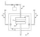
- FIG. 1is a schematic diagram showing an overview of a chemical deposition apparatus 201 in accordance with embodiments disclosed herein.
- a substrate 13sits on top of a movable pedestal module 223 that can be raised or lowered relative to a showerhead module 211 , which may also be moved vertically.
- Reactant material gasesare introduced into a processing zone 318 of the chamber via gas line 203 .
- the apparatusmay be modified to have one or more gas lines, depending on the number of reactant gases used.
- the chamberis evacuated through vacuum lines 235 that are connected to a vacuum source 209 .
- the vacuum sourcemay be a vacuum pump.
- FIG. 2provides a simple block diagram depicting various apparatus components arranged for implementing embodiments disclosed herein wherein plasma is utilized to enhance deposition.
- a processing zone 318serves to contain the plasma generated by a capacitively coupled plasma system including a showerhead module 211 working in conjunction with a pedestal module 223 , wherein the pedestal module 223 is heated.
- RF source(s)such as at least one high-frequency (HF) RF generator 204 , connected to a matching network 206 , and an optional low-frequency (LF) RF generator 202 are connected to the showerhead module 211 .
- HFhigh-frequency
- LFoptional low-frequency
- the HF generator 204can be connected to the pedestal module 223 .
- the power and frequency supplied by matching network 206is sufficient to generate a plasma from the process gas/vapor.
- both the HF generator and the LF generatorare used, and in an alternate embodiment, just the HF generator is used.
- the HF generatoris operated generally at frequencies of about 2-100 MHz; in a preferred embodiment at 13.56 MHz or 27 MHz.
- the LF generatoris operated generally at about 50 kHz to 2 MHz; in a preferred embodiment at about 350 to 600 kHz.
- the process parametersmay be scaled based on the chamber volume, substrate size, and other factors. Similarly, the flow rates of process gas, may depend on the free volume of the vacuum chamber or processing zone.
- the pedestal module 223supports a substrate 13 on which materials such as thin films may be deposited.
- the pedestal module 223can include a fork or lift pins to hold and transfer the substrate during and between the deposition and/or plasma treatment reactions.
- the substrate 13may be configured to rest on a surface of the pedestal module 223 , however in alternate embodiments the pedestal module 223 may include an electrostatic chuck, a mechanical chuck, or a vacuum chuck for holding the substrate 13 on the surface of the pedestal module 223 .
- the pedestal module 223can be coupled with a heater block 220 for heating substrate 13 to a desired temperature. Generally, substrate 13 is maintained at a temperature of about 25° C. to 500° C. or greater depending on the material to be deposited.
- a system controller 228is employed to control process conditions during deposition, post deposition treatments, and/or other process operations.
- the controller 228will typically include one or more memory devices and one or more processors.
- the processormay include a CPU or computer, analog and/or digital input/output connections, stepper motor controller boards, etc.
- the controller 228controls all of the activities of the apparatus.
- the system controller 228executes system control software including sets of instructions for controlling the timing of the processing operations, frequency and power of operations of the LF generator 202 and the HF generator 204 , flow rates and temperatures of precursors and inert gases and their relative mixing, temperature of the heater block 220 and showerhead module 211 , pressure of the chamber, and other parameters of a particular process.
- Other computer programs stored on memory devices associated with the controllermay be employed in some embodiments.
- the user interfacemay include a display screen, graphical software displays of the apparatus and/or process conditions, and user input devices such as pointing devices, keyboards, touch screens, microphones, etc.
- a non-transitory computer machine-readable mediumcan comprise program instructions for control of the apparatus.
- the computer program code for controlling the processing operationscan be written in any conventional computer readable programming language: for example, assembly language, C, C++, Pascal, Fortran or others. Compiled object code or script is executed by the processor to perform the tasks identified in the program.
- the controller parametersrelate to process conditions such as, for example, timing of the processing steps, flow rates and temperatures of precursors and inert gases, temperature of the wafer, pressure of the chamber and other parameters of a particular process. These parameters are provided to the user in the form of a recipe, and may be entered utilizing the user interface.
- Signals for monitoring the processmay be provided by analog and/or digital input connections of the system controller.
- the signals for controlling the processare output on the analog and digital output connections of the apparatus.
- the system softwaremay be designed or configured in many different ways. For example, various chamber component subroutines or control objects may be written to control operation of the chamber components necessary to carry out deposition processes. Examples of programs or sections of programs for this purpose include substrate timing of the processing steps code, flow rates and temperatures of precursors and inert gases code, and a code for pressure of the chamber.
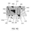
- FIG. 3illustrates a cross section of a chemical isolation chamber 319 including the pedestal module 223 and the showerhead module 211 of FIGS. 1 and 2 in greater detail wherein the pedestal module 223 and showerhead module 211 form a cavity 318 in which a semiconductor substrate is processed.
- the cavity 318is formed between the showerhead module 211 and the pedestal module 223 wherein a lower surface of a faceplate 301 of the showerhead module 211 forms an upper wall and a sidewall of the cavity 318 , and an upper surface of the pedestal module 223 forms a lower wall of the cavity 318 .
- An exemplary embodiment of a deposition apparatus which includes dual chamber sealscan be found in commonly assigned U.S. Pat. No. 7,737,035 which is hereby incorporated by reference in its entirety.
- the pedestal module 223includes a bottom RF electrode 317 and the substrate 13 sits on the pedestal module 223 .
- the bottom RF electrode 317is grounded.
- the distance between the top of the substrate 13 and the bottom surface of the showerhead module 211 during processingis preferably about 5 to 16 millimeters.
- the pedestal module 223includes a heater (see FIG. 2 ) and the faceplate 211 of the showerhead module 211 is heated from heat released from the pedestal module 223 during processing and by plasma struck in the cavity 318 during processing.
- the temperature inside the chambermay be maintained through a heating mechanism in the showerhead module 211 and the pedestal module 223 .
- the substrate 13is located in an isothermal environment.
- An isothermal processing zoneis formed by maintaining each exposed surface of the cavity 318 at a desired temperature.
- the isothermal processing zoneallows the substrate 13 to be uniformly heated and maintained at a desired temperature so that an undesired temperature gradient is not formed across the substrate 13 .
- heat loss from the faceplate 301 to a backing plate 302 and heat loss from the faceplate 301 to an isolation ring 303is minimized.
- the showerhead module 211can be heated to greater than about 250° C.
- the pedestal module 223can be heated to greater than about 250° C. to 500° C. or greater than about 500° C.
- each exposed surface of the cavity 318is formed from a ceramic material.
- the showerhead module 211includes the faceplate 301 , the backing plate 302 , and the isolation ring 303 , wherein the isolation ring surrounds the faceplate 301 and the backing plate 302 and supports the backing plate 302 .
- the isolation ring 303is preferably formed from a ceramic material such as aluminum oxide (Al 2 O 3 ) or aluminum nitride (AlN) and can be supported on a grounded chamber wall 322 of the chemical isolation chamber 319 .
- the backing plate 302is formed from a metal material.
- the backing plate 302can be formed from an aluminum alloy such as Al 6061 or stainless steel wherein the backing plate 302 can include a ceramic outer coating such as an aluminum oxide outer coating, a yttrium oxide outer coating, or a polymeric coating depending on the intended application.
- the backing plate 302is RF hot, i.e., powered by an RF source.
- the backing plate 302can be a cooled backing plate.
- the faceplate 301is preferably formed from a ceramic or metal material and in preferred embodiments can be formed from aluminum oxide (Al 2 O 3 ), or aluminum nitride (AlN).
- the faceplate 301can be electrically conductive or made of ceramic material with an RF electrode 310 embedded therein wherein the embedded RF electrode 310 is preferably a mesh electrode.
- a gas plenum 308is formed between the faceplate 301 and the backing plate 302 .
- the height of the gas plenum 308 between the faceplate 301 and the backing plate 302enables good gas flow from the plenum 308 to the cavity 318 while providing minimal plenum 308 volume.
- the height of the plenum 308is about 2 to 6 mm.
- At least one RF contact 312electrically connects the backing plate 302 and the RF electrode 310 embedded in the faceplate 301 .
- the RF contact 312can be an annular RF contact made of a metallic strip having at least one bend wherein the RF contact 312 forms an outer perimeter of the gas plenum 308 between the faceplate 301 and the backing plate 302 .
- the RF contact 312forms a thermal choke between the faceplate 301 and the backing plate 302 .
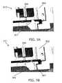
- FIG. 4Aillustrates an exemplary embodiment of a showerhead module 211 and substrate support 223 which form an isothermal processing zone wherein a support element attaches a faceplate of the showerhead module to the backing plate of the showerhead module.
- a support elementattaches a faceplate of the showerhead module to the backing plate of the showerhead module.
- each surface which is exposed to the isothermal processing zoneis a ceramic surface which is maintained at a desired temperature.
- the showerhead module 211includes a faceplate 301 wherein a lower surface of the faceplate forms an upper wall of a cavity 318 and optionally a sidewall of the cavity 318 defining the isothermal processing zone, a backing plate 302 , and an isolation ring 303 , wherein the isolation ring 303 surrounds the faceplate 301 and the backing plate 302 .
- the backing plate 302can include one or more gas inlets 305 and one or more gas outlets 315 (see FIG. 4E ), and the faceplate 301 preferably includes a plurality of through holes 304 for delivering process gas to the isothermal processing zone, delivering inert gas to the isothermal processing zone, or removing process and/or inert gas from the isothermal processing zone.
- the central zone of the faceplate which extends completely over the wafercan include concentric gas inlets and gas outlets to deliver process gas and withdraw reacted gas from the isothermal processing zone.
- concentric inlets and gas outletsto deliver process gas and withdraw reacted gas from the isothermal processing zone.
- At least one compression sealcan be located between the backing plate and the faceplate wherein each compression seal can form a boundary of at least one gas plenum.
- two compression sealscan be used to form gas plenums wherein the first compression seal is a first annular lever seal 306 a which is compressed between the faceplate 301 and the backing plate 302 and wherein the first annular lever seal 306 a forms an inner gas plenum 308 a .
- the inner gas plenum 308 acan be in fluid communication with the one or more gas inlets 305 of the backing plate 302 and a plurality of the through holes 304 of the faceplate 301 such that a process gas can be delivered therethrough into the cavity 318 which defines the isothermal processing zone.
- the second compression sealcan be a second annular lever seal 306 b which surrounds the first annular lever seal 306 a and is compressed between the faceplate 301 and the backing plate 302 wherein the second annular lever seal 306 a forms an intermediate plenum 308 b which surrounds the inner gas plenum 308 a .
- the intermediate plenum 308 bcan be in fluid communication with the one or more gas outlets 315 of the backing plate 302 and a plurality of the through holes 304 of the faceplate 301 such that a process gas can be removed from the isothermal processing zone in cavity 318 by the vacuum source.
- an outer gas plenum 308 csurrounds the intermediate plenum 308 b .
- each annular lever seal 306 a,bprovides a spring force opposing the faceplate 301 and the backing plate 302 wherein each lever seal 306 a,b has at least one bend with a length between a lower free end in contact with the faceplate 301 and an upper free end in contact with the backing plate 302 of about 0.5 to 1.5 inch, and a thickness of about 0.003 to 0.009 inch.
- each lever seal 306 a,bhas an S-shaped, C-shaped, E-shaped, Z-shaped, or V-shaped cross section.
- the faceplate 301is attached to the backing plate 302 with a support element comprising a plurality of cam lock assemblies 309 .
- each cam lock assembly 309is configured to compress each annular lever seal 306 a,b between the faceplate 301 and the backing plate 302 .
- Each compressed annular lever seal 306 a,bforms a thermal choke between the faceplate 301 and the backing plate 302 such that heat loss from the faceplate 301 to the backing plate 302 may be minimized while forming gas plenums 308 a,b,c between the faceplate 301 and the backing plate 302 .
- Each cam lock assembly 309preferably includes a stud (locking pin) 505 mounted into a socket 513 .
- the socket 513can be mounted in a socket hole 513 a in the faceplate.
- the socket 513can include external threads wherein the socket 513 is mounted into the socket hole 513 a which has corresponding internal threads.
- the socket 513may be bonded into the socket hole 513 a .
- the cam lock assembly 309is capable of quickly, cleanly, and accurately attaching the faceplate 301 to the backing plate 302 .
- the stud 505can be formed of a metal or metal alloy including for example stainless steel (such as Nitronic-60) or molybdenum, and may be surrounded by a disc spring stack 515 , such as, for example, stainless steel Belleville washers, or washers formed from alloy such as Haynes 242®.
- the stud 505 and the disc spring stack 515are arranged into the socket 513 such that a limited amount of lateral movement is possible between the faceplate 301 and the backing plate 302 to account for differences in thermal expansion between the two parts.
- each cam lock assembly 309can include a camshaft bearing assembly 507 which is mounted in a backing plate bore 511 of the backing plate 302 which is configured to receive the stud 505 .
- An exemplary embodiment of a cam lock assembly which can be used to couple a faceplate of a showerhead module to a backing plate of the showerhead modulecan be found in commonly assigned U.S. Pat. No. 8,272,346, which is incorporated by reference herein in its entirety.
- Each cam lock assembly 309can include an electrically conductive socket which forms an RF contact 312 , wherein the RF contact 312 electrically connects the RF electrode 310 of the faceplate 301 with the backing plate 302 which is RF hot.
- Each RF contact 312can be formed of metal or any suitable conducting material, however in a preferred embodiment, each RF contact 312 is formed from tungsten. Alternatively, each RF contact 312 can be formed from stainless steel or an austenitic nickel-chromium base alloy. Further, each RF contact 312 can include a nickel outer coating.
- Each cam lock assembly 309preferably provides a minimum contact area between the faceplate 301 and the backing plate 302 such that the faceplate 301 can be thermally isolated from the remainder of the showerhead module 211 .
- Thermally isolating the faceplate 301 of the showerhead module 211reduces heat loss from an upper surface thereof to the backing plate 302 as well as heat loss at an outer periphery thereof to the isolation ring 303 which surrounds the faceplate 301 , thereby forming an isothermal processing zone in cavity 318 .
- Thermally isolating the faceplate 301allows a desired temperature to be maintained across the lower surface of the faceplate 301 and leads to more uniform substrate processing.
- the contact area between the support element (cam locks) and the faceplateis less than 1% of the total surface area of the faceplate.
- the total contact areais less than 0.5% of the total surface area of the faceplate, less than 0.3% of the total surface area of the faceplate, less than 0.2% of the total surface area of the faceplate, less than 0.1% of the total surface area of the faceplate; or less than 0.05% of the total surface area of the faceplate.
- the RF contact 312may form the socket of the cam lock assembly 309 , wherein a lower portion 312 a of the RF contact 312 can be mounted in the faceplate 301 so as to minimize the contact area between the faceplate 301 and the backing plate 302 and provide reduced thermal transfer therebetween.
- the lower portion 312 a of the RF contact 312is preferably brazed to the embedded RF electrode 310 .
- FIG. 4Billustrates an embodiment of a showerhead module 211 and substrate support 223 which are configured to form an isothermal processing zone in the cavity 318 which has an improved RF profile.
- the bottom RF electrode 317 of the pedestal module 223can be lengthened such that is extends to the outer periphery, or beyond the outer periphery of the cavity 318 . Extending the bottom RF electrode 317 , which is preferably a grounded electrode, beyond the periphery of the cavity 318 reduces the strength of the electric field between the pedestal module 223 and a surrounding grounded chamber wall 322 such that the potential for arcing therebetween is also reduced.
- the bottom RF electrode 317has a diameter greater than about 12.5 inches and more preferably the bottom RF electrode 317 has a diameter greater than about 15 inches such as a diameter of about 15.6 inches.
- the isolation ring 303includes a support element which attaches the faceplate 301 to the backing plate 302 , and compresses each annular lever seal 306 a,b therebetween wherein the isolation ring 303 includes an inner annular flange 313 which underlies an outer portion of the faceplate 301 and the inner annular flange 313 has at least one upwardly extending projection 314 located thereon which supports the faceplate 301 .
- the at least one upwardly extending projection 314contacts the faceplate 301 and provides a thermal choke which biases the faceplate 301 against the backing plate 302 (i.e. maintains the faceplate 301 parallel with respect to the backing plate 302 ).
- At least three upwardly extending projections 314support the faceplate 301 .
- the at least one upwardly extending projection 314minimizes the contact area between the isolation ring 303 and the faceplate 301 , such that the faceplate 301 may be thermally isolated from the isolation ring 303 at an outer periphery thereof as well as the remainder of the showerhead module 211 .
- Thermally isolating the faceplate 301 from the remainder of the showerhead module 211can provide an isothermal processing zone in cavity 318 which leads to more uniform substrate processing.
- the maximum total contact area between the at least one upwardly extending projection 314 of the isolation ring 303 and the faceplate 301is less than about 0.05 in 2 , and preferably less than about 0.02 in 2 , and more preferably less than about 0.01 in 2 .
- the isolation ring 303is configured to compress the first annular lever seal 306 a between the faceplate 301 and the backing plate 302 so as to form the inner gas plenum 308 a , and to compress the second annular lever seal 306 b so as to form the intermediate gas plenum 308 b .
- an upper surface of the faceplate 301can include annular recesses 360 wherein a lower portion of each annular lever seal 306 a,b is supported in a respective annular recess 360 .
- a lower surface of the backing plate 302can also include annular recesses 360 wherein an upper portion of each annular lever seal 306 a,b is supported in a respective annular recess 360 .
- An RF contact 312electrically connects the RF electrode 310 embedded in the faceplate 301 with the backing plate 302 which is RF hot.
- the RF contact 312can be formed of any suitable conducting material such as, stainless steel, tungsten, an austenitic nickel-chromium based alloy preferably including an outer nickel plating such as nickel plated Inconel®, and the like.
- the RF contact 312is an annular RF contact made of a metallic strip having at least one bend wherein the RF contact is electrically connected to an RF electrode embedded in the ceramic faceplate and wherein the annular RF contact surrounds the second annular lever seal 306 b and forms the outer perimeter of an outer gas plenum 308 c between the backing plate 302 and the faceplate 301 .
- a gas inlet 305 in the backing plate 302can be configured to deliver an inert gas to the outer gas plenum 308 c wherein the inert gas can then be delivered to an outer periphery of the cavity 318 via through holes 304 in the faceplate 301 which are in fluid communication with the outer gas plenum 308 c .
- the RF contact 312has at least one bend compressible therein wherein the diameter of the bend is configured to minimize the potential for arcing between an inner surface 303 a of the isolation ring 303 and an outer surface of the RF contact 312 .
- the support elementcomprises an RF contact 312 which attaches the faceplate 301 to the backing plate 302 as well as electrically connect the faceplate 301 to the backing plate 302 .
- the RF contact 312is preferably an annular RF contact made of a metallic strip having at least one bend wherein the RF contact 312 provides a clamping force between the faceplate 301 and the backing plate 302 to compress lever seals 306 a,b .
- the at least one bendpreferably has a diameter configured to minimize a potential for arcing between an inner surface 303 a of the isolation ring 303 and an outer surface of the RF contact 312 .
- the annular RF contact 312forms the outer perimeter of the outer gas plenum 308 c between the backing plate 302 and the faceplate 301 .
- a lower end of the RF contact 312is preferably brazed to an exposed portion of the RF electrode 310 embedded in the faceplate 301 , while an upper end of the RF contact 312 is preferably attached to the backing plate 302 with suitable mechanical fasteners 320 , which can be threaded bolts, screws, or the like.
- suitable mechanical fasteners 320can be threaded bolts, screws, or the like.
- about 9 to 12 mechanical fasteners 320may attach the upper end of the RF contact 312 to the backing plate 302 , however in an alternate embodiment more fasteners 320 may be utilized.
- the RF contact 312preferably has a length between a lower free end in contact with the faceplate and an upper free end in contact with the backing plate of about 0.5 to 1.5 inch, and a thickness of about 0.003 to 0.009 inch.
- the RF contacthas an S-shaped, C-shaped, E-shaped, Z-shaped, or V-shaped cross section.
- the RF contact 312can be formed of any suitable conducting material such as, stainless steel, tungsten, an austenitic nickel-chromium based alloy and the RF contact 312 preferably includes an outer nickel plating such as nickel plated Inconel®, and the like.
- the faceplate 301preferably includes at least one upwardly extending spacer 307 (See FIG. 5A ) on an upper surface 301 a at an outer periphery thereof, wherein the at least one upwardly extending spacer 307 maintains a desired plenum height between the faceplate 301 and the backing plate 302 and wherein the at least one spacer 307 is configured to maintain the faceplate 301 parallel with respect to the backing plate 302 .
- at least three upwardly extending spacers 307are located between the faceplate 301 and the backing plate 302 .
- the at least one spacer 307can be provided on the lower surface 302 a of the backing plate 302 in a downwardly extending fashion.
- the spacer 307can be a sapphire ball which is pressed into the lower surface 302 a of the backing plate 302 .
- the total contact area between the at least one upwardly extending spacer 307 of the faceplate 301 and the backing plate 302is less than about 0.5 in 2 , preferably less than about 0.05 in 2 , and more preferably less than about 0.01 in 2 .
- FIG. 5Billustrates an embodiment of the showerhead module 211 , wherein at least one spacer 307 is located between the faceplate 301 and the backing plate 302 wherein the spacer 307 maintains a desired gas plenum height therebetween wherein the at least one spacer 307 is configured to maintain the faceplate 301 parallel with respect to the backing plate 302 .
- Preferably at least three spacers 307are located between the faceplate 301 and the backing plate 302 .
- the spacers 307can be integral to the faceplate 301 (See FIG.
- the spacers 307can be spheres located in an outer periphery of the gas plenum 308 , wherein the spacers 307 are freely movable such that they may allow for thermal expansion and contraction of the faceplate 301 and the backing plate 302 such that a desired plenum height therebetween may be maintained.
- the spacers 307are formed from a ceramic material.
- the spacers 307can be formed from quartz or sapphire.
- FIG. 6illustrates an embodiment of the showerhead module 211 wherein the RF contact 312 forms a friction contact with a metalized surface 401 of the faceplate 301 which is in electrical contact with the RF electrode 310 embedded in the faceplate 301 , wherein the RF contact 312 electrically connects the RF electrode 310 of the faceplate 301 with the backing plate 302 which is RF hot.
- the lower surface of the faceplate 301forms an upper wall of the cavity 318 wherein the lower surface of the faceplate 301 includes a ring 402 of like material around an outer periphery thereof wherein an inner surface of the ring 402 forms a sidewall of the cavity 318 defining the isothermal processing zone in cavity 318 .
- the ring 402is bonded or mechanically attached with suitable fasteners, such as screws 403 , to the lower surface of the faceplate 301 .
Landscapes
- Chemical & Material Sciences (AREA)
- Engineering & Computer Science (AREA)
- Chemical Kinetics & Catalysis (AREA)
- General Chemical & Material Sciences (AREA)
- Materials Engineering (AREA)
- Mechanical Engineering (AREA)
- Metallurgy (AREA)
- Organic Chemistry (AREA)
- Physics & Mathematics (AREA)
- Plasma & Fusion (AREA)
- Analytical Chemistry (AREA)
- Chemical Vapour Deposition (AREA)
- Condensed Matter Physics & Semiconductors (AREA)
- General Physics & Mathematics (AREA)
- Manufacturing & Machinery (AREA)
- Computer Hardware Design (AREA)
- Microelectronics & Electronic Packaging (AREA)
- Power Engineering (AREA)
Abstract
Description
- This invention pertains to apparatuses for conducting chemical depositions, and may find particular use in conducting plasma enhanced chemical depositions of thin films.
- Plasma processing apparatuses are used to process semiconductor substrates by techniques including etching, physical vapor deposition (PVD), chemical vapor deposition (CVD), plasma enhanced chemical vapor deposition (PECVD), atomic layer deposition (ALD), plasma enhanced atomic layer deposition (PEALD), pulsed deposition layer (PDL), plasma enhanced pulsed deposition layer (PEPDL) processing, and resist removal. One type of plasma processing apparatus used in plasma processing includes a reaction chamber containing top and bottom electrodes. A radio frequency (RF) power is applied between the electrodes to excite a process gas into a plasma for processing semiconductor substrates in the reaction chamber. In such chambers nonuniform heating across a semiconductor substrate can lead to nonuniform substrate processing.
- Disclosed herein is a deposition apparatus for processing semiconductor substrates wherein the deposition apparatus has an isothermal processing zone. The deposition apparatus comprises a chemical isolation chamber in which semiconductor substrates are processed. A process gas source is in fluid communication with the chemical isolation chamber for supplying a process gas into the chemical isolation chamber wherein a showerhead module delivers process gases from the process gas source to the isothermal processing zone. The showerhead module includes a faceplate wherein a lower surface of the faceplate forms an upper wall of a cavity defining the isothermal processing zone, a backing plate, an isolation ring which surrounds the faceplate and the backing plate wherein the isolation ring supports the backing plate, a support element which attaches the faceplate to the backing plate, and at least one compression seal which forms an outer perimeter of a central gas plenum between the faceplate and the backing plate. A contact area between the support element and the faceplate is less than 1% of the total surface area of the faceplate. A substrate pedestal module is configured to heat and support a semiconductor substrate wherein an upper surface of the pedestal module forms a lower wall of the cavity defining the isothermal processing zone within the chemical isolation chamber, and an evacuation apparatus is in fluid communication with the isothermal processing zone for evacuating process gas from the processing zone.
- Also disclosed herein is a showerhead module of a plasma processing apparatus. The showerhead module delivers process gases from a process gas source to an isothermal processing zone. The showerhead module includes a faceplate wherein a lower surface of the faceplate forms an upper wall of a cavity defining the isothermal processing zone, a backing plate, an isolation ring which surrounds the faceplate and the backing plate wherein the isolation ring supports the backing plate, a support element which attaches the faceplate to the backing plate, and at least one compression seal which forms an outer perimeter of a central gas plenum between the faceplate and the backing plate. A contact area between the support element and the faceplate is less than 1% of the total surface area of the faceplate.
FIG. 1 illustrates a schematic diagram showing an overview of a chemical deposition apparatus in accordance with embodiments disclosed herein.FIG. 2 illustrates a block diagram depicting various apparatus components arranged for implementing embodiments disclosed herein wherein plasma can be utilized to enhance deposition and/or surface reactions between reacting species during the generation of thin films.FIG. 3 illustrates a cross section of the pedestal module and the showerhead module arranged in accordance with embodiments disclosed herein.FIGS. 4A-4E each illustrate a cross section of a showerhead module arranged in accordance with embodiments disclosed herein.FIGS. 5A ,5B each illustrate a cross section of a showerhead module arranged in accordance with embodiments disclosed herein.FIG. 6 illustrates a cross section of a showerhead module arranged in accordance with embodiments disclosed herein.- In the following detailed description, numerous specific embodiments are set forth in order to provide a thorough understanding of the apparatus and methods disclosed herein. However, as will be apparent to those skilled in the art, that the present embodiments may be practiced without these specific details or by using alternate elements or processes. In other instances, well-known processes, procedures, and/or components have not been described in detail so as not to unnecessarily obscure aspects of embodiments disclosed herein. As used herein the term “about” refers to ±10%.
- As indicated, present embodiments provide apparatus and associated methods for conducting a chemical deposition such as a plasma enhanced chemical vapor deposition. The apparatus and methods are particularly applicable for use in conjunction with semiconductor fabrication based dielectric deposition processes which require separation of self-limiting deposition steps in a multi-step deposition process (e.g., atomic layer deposition (ALD), plasma enhanced atomic layer deposition (PEALD), plasma enhanced chemical vapor deposition (PECVD), pulsed deposition layer (PDL), or plasma enhanced pulsed deposition layer (PEPDL) processing), however they are not so limited.
- The aforementioned processes can suffer from some drawbacks associated with nonuniform temperatures across a wafer or substrate receiving deposited material. For example, nonuniform temperatures may develop across a substrate when a passively heated showerhead, which is in thermal contact with surrounding chamber components, loses heat to the surrounding components. Therefore, the showerhead which forms an upper wall of a processing zone is preferably thermally isolated from the surrounding components such that an isothermal processing zone may be formed, thereby forming uniform temperatures across the substrate and uniform temperatures across the showerhead face (i.e. upper wall of the processing zone). The uniform temperatures across the substrate aid in the uniform processing of semiconductor substrates wherein the substrate temperature provides activation energy for the deposition process and is therefore a control means for driving the deposition reaction. The uniform temperatures across the showerhead also aid in uniform gas phase reactions above a semiconductor substrate. The uniform temperatures also aid in choice of materials with lower thermal conductivity but higher corrosion resistance.
- Further, there are generally two main types of deposition showerheads: the chandelier type and the flush mount. The chandelier showerheads have a stem attached to the top of the chamber on one end and the faceplate on the other end, resembling a chandelier. A part of the stem may protrude the chamber top to enable connection of gas lines and RF power. Thus, larger chamber volumes which must be evacuated during processing, such as those required by the chandelier design, can become throughput prohibitive. The flush mount showerheads, however, are integrated into the top of a chamber and do not have a stem, and therefore, the chamber volume which must be evacuated can be reduced. Present embodiments disclosed herein pertain to a flush mount type showerhead wherein the flush mount showerhead reduces chamber volume which must be evacuated by a vacuum source during processing. The flush mount showerheads can lose heat from the showerhead face and body to the rest of the chamber through conduction. This not only lowers the temperature of the faceplate of the showerhead, but also introduces radial temperature non-uniformities in the showerhead face exposed to the processing zone. Embodiments disclosed herein reduce heat loss from the showerhead to the chamber through conduction, and increase radial temperature uniformity of the face of the showerhead exposed to the processing zone, thereby forming an isothermal processing zone.
FIG. 1 is a schematic diagram showing an overview of achemical deposition apparatus 201 in accordance with embodiments disclosed herein. Asubstrate 13 sits on top of amovable pedestal module 223 that can be raised or lowered relative to ashowerhead module 211, which may also be moved vertically. Reactant material gases are introduced into aprocessing zone 318 of the chamber viagas line 203. Note that the apparatus may be modified to have one or more gas lines, depending on the number of reactant gases used. The chamber is evacuated throughvacuum lines 235 that are connected to avacuum source 209. The vacuum source may be a vacuum pump.- Embodiments disclosed herein are preferably implemented in a plasma enhanced chemical deposition apparatus (i.e. PECVD apparatus, PEALD apparatus, or PEPDL apparatus).
FIG. 2 provides a simple block diagram depicting various apparatus components arranged for implementing embodiments disclosed herein wherein plasma is utilized to enhance deposition. As shown, aprocessing zone 318 serves to contain the plasma generated by a capacitively coupled plasma system including ashowerhead module 211 working in conjunction with apedestal module 223, wherein thepedestal module 223 is heated. RF source(s), such as at least one high-frequency (HF)RF generator 204, connected to amatching network 206, and an optional low-frequency (LF)RF generator 202 are connected to theshowerhead module 211. In an alternative embodiment, theHF generator 204 can be connected to thepedestal module 223. The power and frequency supplied by matchingnetwork 206 is sufficient to generate a plasma from the process gas/vapor. In an embodiment both the HF generator and the LF generator are used, and in an alternate embodiment, just the HF generator is used. In a typical process, the HF generator is operated generally at frequencies of about 2-100 MHz; in a preferred embodiment at 13.56 MHz or 27 MHz. The LF generator is operated generally at about 50 kHz to 2 MHz; in a preferred embodiment at about 350 to 600 kHz. The process parameters may be scaled based on the chamber volume, substrate size, and other factors. Similarly, the flow rates of process gas, may depend on the free volume of the vacuum chamber or processing zone. - Within the chamber, the
pedestal module 223 supports asubstrate 13 on which materials such as thin films may be deposited. Thepedestal module 223 can include a fork or lift pins to hold and transfer the substrate during and between the deposition and/or plasma treatment reactions. In an embodiment, thesubstrate 13 may be configured to rest on a surface of thepedestal module 223, however in alternate embodiments thepedestal module 223 may include an electrostatic chuck, a mechanical chuck, or a vacuum chuck for holding thesubstrate 13 on the surface of thepedestal module 223. Thepedestal module 223 can be coupled with a heater block220 forheating substrate 13 to a desired temperature. Generally,substrate 13 is maintained at a temperature of about 25° C. to 500° C. or greater depending on the material to be deposited. - In certain embodiments, a
system controller 228 is employed to control process conditions during deposition, post deposition treatments, and/or other process operations. Thecontroller 228 will typically include one or more memory devices and one or more processors. The processor may include a CPU or computer, analog and/or digital input/output connections, stepper motor controller boards, etc. - In certain embodiments, the
controller 228 controls all of the activities of the apparatus. Thesystem controller 228 executes system control software including sets of instructions for controlling the timing of the processing operations, frequency and power of operations of theLF generator 202 and theHF generator 204, flow rates and temperatures of precursors and inert gases and their relative mixing, temperature of the heater block220 andshowerhead module 211, pressure of the chamber, and other parameters of a particular process. Other computer programs stored on memory devices associated with the controller may be employed in some embodiments. - Typically there will be a user interface associated with
controller 228. The user interface may include a display screen, graphical software displays of the apparatus and/or process conditions, and user input devices such as pointing devices, keyboards, touch screens, microphones, etc. - A non-transitory computer machine-readable medium can comprise program instructions for control of the apparatus. The computer program code for controlling the processing operations can be written in any conventional computer readable programming language: for example, assembly language, C, C++, Pascal, Fortran or others. Compiled object code or script is executed by the processor to perform the tasks identified in the program.
- The controller parameters relate to process conditions such as, for example, timing of the processing steps, flow rates and temperatures of precursors and inert gases, temperature of the wafer, pressure of the chamber and other parameters of a particular process. These parameters are provided to the user in the form of a recipe, and may be entered utilizing the user interface.
- Signals for monitoring the process may be provided by analog and/or digital input connections of the system controller. The signals for controlling the process are output on the analog and digital output connections of the apparatus.
- The system software may be designed or configured in many different ways. For example, various chamber component subroutines or control objects may be written to control operation of the chamber components necessary to carry out deposition processes. Examples of programs or sections of programs for this purpose include substrate timing of the processing steps code, flow rates and temperatures of precursors and inert gases code, and a code for pressure of the chamber.
FIG. 3 illustrates a cross section of achemical isolation chamber 319 including thepedestal module 223 and theshowerhead module 211 ofFIGS. 1 and 2 in greater detail wherein thepedestal module 223 andshowerhead module 211 form acavity 318 in which a semiconductor substrate is processed. Thecavity 318 is formed between theshowerhead module 211 and thepedestal module 223 wherein a lower surface of afaceplate 301 of theshowerhead module 211 forms an upper wall and a sidewall of thecavity 318, and an upper surface of thepedestal module 223 forms a lower wall of thecavity 318. An exemplary embodiment of a deposition apparatus which includes dual chamber seals can be found in commonly assigned U.S. Pat. No. 7,737,035 which is hereby incorporated by reference in its entirety.- The
pedestal module 223 includes abottom RF electrode 317 and thesubstrate 13 sits on thepedestal module 223. Preferably thebottom RF electrode 317 is grounded. The distance between the top of thesubstrate 13 and the bottom surface of theshowerhead module 211 during processing is preferably about 5 to 16 millimeters. Thepedestal module 223 includes a heater (seeFIG. 2 ) and thefaceplate 211 of theshowerhead module 211 is heated from heat released from thepedestal module 223 during processing and by plasma struck in thecavity 318 during processing. In some embodiments, the temperature inside the chamber may be maintained through a heating mechanism in theshowerhead module 211 and thepedestal module 223. Preferably, thesubstrate 13 is located in an isothermal environment. An isothermal processing zone is formed by maintaining each exposed surface of thecavity 318 at a desired temperature. The isothermal processing zone allows thesubstrate 13 to be uniformly heated and maintained at a desired temperature so that an undesired temperature gradient is not formed across thesubstrate 13. To form the isothermal processing zone, heat loss from thefaceplate 301 to abacking plate 302 and heat loss from thefaceplate 301 to anisolation ring 303 is minimized. In an embodiment, theshowerhead module 211 can be heated to greater than about 250° C., and/or thepedestal module 223 can be heated to greater than about 250° C. to 500° C. or greater than about 500° C. In a preferred embodiment, each exposed surface of thecavity 318 is formed from a ceramic material. - The
showerhead module 211 includes thefaceplate 301, thebacking plate 302, and theisolation ring 303, wherein the isolation ring surrounds thefaceplate 301 and thebacking plate 302 and supports thebacking plate 302. Theisolation ring 303 is preferably formed from a ceramic material such as aluminum oxide (Al2O3) or aluminum nitride (AlN) and can be supported on a groundedchamber wall 322 of thechemical isolation chamber 319. - The
backing plate 302 is formed from a metal material. For example thebacking plate 302 can be formed from an aluminum alloy such as Al6061 or stainless steel wherein thebacking plate 302 can include a ceramic outer coating such as an aluminum oxide outer coating, a yttrium oxide outer coating, or a polymeric coating depending on the intended application. In a preferred embodiment, thebacking plate 302 is RF hot, i.e., powered by an RF source. In an embodiment, thebacking plate 302 can be a cooled backing plate. Thefaceplate 301 is preferably formed from a ceramic or metal material and in preferred embodiments can be formed from aluminum oxide (Al2O3), or aluminum nitride (AlN). Thefaceplate 301 can be electrically conductive or made of ceramic material with anRF electrode 310 embedded therein wherein the embeddedRF electrode 310 is preferably a mesh electrode. Agas plenum 308 is formed between thefaceplate 301 and thebacking plate 302. Preferably the height of thegas plenum 308 between thefaceplate 301 and thebacking plate 302 enables good gas flow from theplenum 308 to thecavity 318 while providingminimal plenum 308 volume. Preferably the height of theplenum 308 is about 2 to 6 mm. At least oneRF contact 312 electrically connects thebacking plate 302 and theRF electrode 310 embedded in thefaceplate 301. In an embodiment, theRF contact 312 can be an annular RF contact made of a metallic strip having at least one bend wherein theRF contact 312 forms an outer perimeter of thegas plenum 308 between thefaceplate 301 and thebacking plate 302. Preferably theRF contact 312 forms a thermal choke between thefaceplate 301 and thebacking plate 302. FIG. 4A illustrates an exemplary embodiment of ashowerhead module 211 andsubstrate support 223 which form an isothermal processing zone wherein a support element attaches a faceplate of the showerhead module to the backing plate of the showerhead module. Preferably each surface which is exposed to the isothermal processing zone is a ceramic surface which is maintained at a desired temperature. Theshowerhead module 211 includes afaceplate 301 wherein a lower surface of the faceplate forms an upper wall of acavity 318 and optionally a sidewall of thecavity 318 defining the isothermal processing zone, abacking plate 302, and anisolation ring 303, wherein theisolation ring 303 surrounds thefaceplate 301 and thebacking plate 302. Thebacking plate 302 can include one ormore gas inlets 305 and one or more gas outlets315 (seeFIG. 4E ), and thefaceplate 301 preferably includes a plurality of throughholes 304 for delivering process gas to the isothermal processing zone, delivering inert gas to the isothermal processing zone, or removing process and/or inert gas from the isothermal processing zone.- For example, the central zone of the faceplate which extends completely over the wafer can include concentric gas inlets and gas outlets to deliver process gas and withdraw reacted gas from the isothermal processing zone. A suitable arrangement of concentric inlets and outlets is disclosed in U.S. Pat. No. 5,102,523 or 5,614,026, incorporated herein by reference.
- At least one compression seal can be located between the backing plate and the faceplate wherein each compression seal can form a boundary of at least one gas plenum. For example, two compression seals can be used to form gas plenums wherein the first compression seal is a first
annular lever seal 306awhich is compressed between thefaceplate 301 and thebacking plate 302 and wherein the firstannular lever seal 306aforms aninner gas plenum 308a. Theinner gas plenum 308acan be in fluid communication with the one ormore gas inlets 305 of thebacking plate 302 and a plurality of the throughholes 304 of thefaceplate 301 such that a process gas can be delivered therethrough into thecavity 318 which defines the isothermal processing zone. The second compression seal can be a secondannular lever seal 306bwhich surrounds the firstannular lever seal 306aand is compressed between thefaceplate 301 and thebacking plate 302 wherein the secondannular lever seal 306aforms anintermediate plenum 308bwhich surrounds theinner gas plenum 308a. Theintermediate plenum 308bcan be in fluid communication with the one ormore gas outlets 315 of thebacking plate 302 and a plurality of the throughholes 304 of thefaceplate 301 such that a process gas can be removed from the isothermal processing zone incavity 318 by the vacuum source. In an embodiment, anouter gas plenum 308csurrounds theintermediate plenum 308b. Preferably theouter gas plenum 308ccan deliver inert gas to a gap between thefaceplate 301 and theisolation ring 303 which is in fluid communication with the isothermal processing zone incavity 318 and wherein theisolation ring 303 forms an outer periphery of theouter gas plenum 308c. Preferably eachannular lever seal 306a,bprovides a spring force opposing thefaceplate 301 and thebacking plate 302 wherein eachlever seal 306a,bhas at least one bend with a length between a lower free end in contact with thefaceplate 301 and an upper free end in contact with thebacking plate 302 of about 0.5 to 1.5 inch, and a thickness of about 0.003 to 0.009 inch. Preferably eachlever seal 306a,bhas an S-shaped, C-shaped, E-shaped, Z-shaped, or V-shaped cross section. - In an embodiment, the
faceplate 301 is attached to thebacking plate 302 with a support element comprising a plurality ofcam lock assemblies 309. When coupled, eachcam lock assembly 309 is configured to compress eachannular lever seal 306a,bbetween thefaceplate 301 and thebacking plate 302. Each compressedannular lever seal 306a,bforms a thermal choke between thefaceplate 301 and thebacking plate 302 such that heat loss from thefaceplate 301 to thebacking plate 302 may be minimized while forminggas plenums 308a,b,cbetween thefaceplate 301 and thebacking plate 302. - Each
cam lock assembly 309 preferably includes a stud (locking pin)505 mounted into asocket 513. Thesocket 513 can be mounted in a socket hole513ain the faceplate. In an embodiment, thesocket 513 can include external threads wherein thesocket 513 is mounted into the socket hole513awhich has corresponding internal threads. Alternatively thesocket 513 may be bonded into the socket hole513a. Thecam lock assembly 309 is capable of quickly, cleanly, and accurately attaching thefaceplate 301 to thebacking plate 302. Thestud 505 can be formed of a metal or metal alloy including for example stainless steel (such as Nitronic-60) or molybdenum, and may be surrounded by adisc spring stack 515, such as, for example, stainless steel Belleville washers, or washers formed from alloy such as Haynes 242®. Thestud 505 and thedisc spring stack 515 are arranged into thesocket 513 such that a limited amount of lateral movement is possible between thefaceplate 301 and thebacking plate 302 to account for differences in thermal expansion between the two parts. - Other portions of each
cam lock assembly 309 can include acamshaft bearing assembly 507 which is mounted in a backing plate bore511 of thebacking plate 302 which is configured to receive thestud 505. An exemplary embodiment of a cam lock assembly which can be used to couple a faceplate of a showerhead module to a backing plate of the showerhead module can be found in commonly assigned U.S. Pat. No. 8,272,346, which is incorporated by reference herein in its entirety. - Each
cam lock assembly 309 can include an electrically conductive socket which forms anRF contact 312, wherein theRF contact 312 electrically connects theRF electrode 310 of thefaceplate 301 with thebacking plate 302 which is RF hot. EachRF contact 312 can be formed of metal or any suitable conducting material, however in a preferred embodiment, eachRF contact 312 is formed from tungsten. Alternatively, each RF contact312 can be formed from stainless steel or an austenitic nickel-chromium base alloy. Further, each RF contact312 can include a nickel outer coating. Eachcam lock assembly 309 preferably provides a minimum contact area between thefaceplate 301 and thebacking plate 302 such that thefaceplate 301 can be thermally isolated from the remainder of theshowerhead module 211. Thermally isolating thefaceplate 301 of theshowerhead module 211 reduces heat loss from an upper surface thereof to thebacking plate 302 as well as heat loss at an outer periphery thereof to theisolation ring 303 which surrounds thefaceplate 301, thereby forming an isothermal processing zone incavity 318. Thermally isolating thefaceplate 301 allows a desired temperature to be maintained across the lower surface of thefaceplate 301 and leads to more uniform substrate processing. The contact area between the support element (cam locks) and the faceplate is less than 1% of the total surface area of the faceplate. Preferably the total contact area is less than 0.5% of the total surface area of the faceplate, less than 0.3% of the total surface area of the faceplate, less than 0.2% of the total surface area of the faceplate, less than 0.1% of the total surface area of the faceplate; or less than 0.05% of the total surface area of the faceplate. As illustrated inFIG. 4C , theRF contact 312 may form the socket of thecam lock assembly 309, wherein alower portion 312aof theRF contact 312 can be mounted in thefaceplate 301 so as to minimize the contact area between thefaceplate 301 and thebacking plate 302 and provide reduced thermal transfer therebetween. Thelower portion 312aof theRF contact 312 is preferably brazed to the embeddedRF electrode 310. FIG. 4B illustrates an embodiment of ashowerhead module 211 andsubstrate support 223 which are configured to form an isothermal processing zone in thecavity 318 which has an improved RF profile. As illustrated inFIG. 4B , thebottom RF electrode 317 of thepedestal module 223 can be lengthened such that is extends to the outer periphery, or beyond the outer periphery of thecavity 318. Extending thebottom RF electrode 317, which is preferably a grounded electrode, beyond the periphery of thecavity 318 reduces the strength of the electric field between thepedestal module 223 and a surrounding groundedchamber wall 322 such that the potential for arcing therebetween is also reduced. Preferably, thebottom RF electrode 317 has a diameter greater than about 12.5 inches and more preferably thebottom RF electrode 317 has a diameter greater than about 15 inches such as a diameter of about 15.6 inches.- In an embodiment, as illustrated in
FIG. 4D , theisolation ring 303 includes a support element which attaches thefaceplate 301 to thebacking plate 302, and compresses eachannular lever seal 306a,btherebetween wherein theisolation ring 303 includes an innerannular flange 313 which underlies an outer portion of thefaceplate 301 and the innerannular flange 313 has at least one upwardly extendingprojection 314 located thereon which supports thefaceplate 301. The at least one upwardly extendingprojection 314 contacts thefaceplate 301 and provides a thermal choke which biases thefaceplate 301 against the backing plate302 (i.e. maintains thefaceplate 301 parallel with respect to the backing plate302). Preferably at least three upwardly extendingprojections 314 support thefaceplate 301. The at least one upwardly extendingprojection 314 minimizes the contact area between theisolation ring 303 and thefaceplate 301, such that thefaceplate 301 may be thermally isolated from theisolation ring 303 at an outer periphery thereof as well as the remainder of theshowerhead module 211. Thermally isolating thefaceplate 301 from the remainder of theshowerhead module 211 can provide an isothermal processing zone incavity 318 which leads to more uniform substrate processing. The maximum total contact area between the at least one upwardly extendingprojection 314 of theisolation ring 303 and thefaceplate 301 is less than about 0.05 in2, and preferably less than about 0.02 in2, and more preferably less than about 0.01 in2. When attached, theisolation ring 303 is configured to compress the firstannular lever seal 306abetween thefaceplate 301 and thebacking plate 302 so as to form theinner gas plenum 308a, and to compress the secondannular lever seal 306bso as to form theintermediate gas plenum 308b. In an embodiment, an upper surface of thefaceplate 301 can includeannular recesses 360 wherein a lower portion of eachannular lever seal 306a,bis supported in a respectiveannular recess 360. In a further embodiment, a lower surface of thebacking plate 302 can also includeannular recesses 360 wherein an upper portion of eachannular lever seal 306a,bis supported in a respectiveannular recess 360. AnRF contact 312 electrically connects theRF electrode 310 embedded in thefaceplate 301 with thebacking plate 302 which is RF hot. TheRF contact 312 can be formed of any suitable conducting material such as, stainless steel, tungsten, an austenitic nickel-chromium based alloy preferably including an outer nickel plating such as nickel plated Inconel®, and the like. In a preferred embodiment, theRF contact 312 is an annular RF contact made of a metallic strip having at least one bend wherein the RF contact is electrically connected to an RF electrode embedded in the ceramic faceplate and wherein the annular RF contact surrounds the secondannular lever seal 306band forms the outer perimeter of anouter gas plenum 308cbetween thebacking plate 302 and thefaceplate 301. Agas inlet 305 in thebacking plate 302 can be configured to deliver an inert gas to theouter gas plenum 308cwherein the inert gas can then be delivered to an outer periphery of thecavity 318 via throughholes 304 in thefaceplate 301 which are in fluid communication with theouter gas plenum 308c. TheRF contact 312 has at least one bend compressible therein wherein the diameter of the bend is configured to minimize the potential for arcing between aninner surface 303aof theisolation ring 303 and an outer surface of theRF contact 312. - In an embodiment, as illustrated in
FIG. 4E , the support element comprises anRF contact 312 which attaches thefaceplate 301 to thebacking plate 302 as well as electrically connect thefaceplate 301 to thebacking plate 302. TheRF contact 312 is preferably an annular RF contact made of a metallic strip having at least one bend wherein theRF contact 312 provides a clamping force between thefaceplate 301 and thebacking plate 302 to compresslever seals 306a,b. The at least one bend preferably has a diameter configured to minimize a potential for arcing between aninner surface 303aof theisolation ring 303 and an outer surface of theRF contact 312. Theannular RF contact 312 forms the outer perimeter of theouter gas plenum 308cbetween thebacking plate 302 and thefaceplate 301. A lower end of theRF contact 312 is preferably brazed to an exposed portion of theRF electrode 310 embedded in thefaceplate 301, while an upper end of theRF contact 312 is preferably attached to thebacking plate 302 with suitablemechanical fasteners 320, which can be threaded bolts, screws, or the like. In a preferred embodiment, about 9 to 12mechanical fasteners 320 may attach the upper end of theRF contact 312 to thebacking plate 302, however in an alternate embodimentmore fasteners 320 may be utilized. TheRF contact 312 preferably has a length between a lower free end in contact with the faceplate and an upper free end in contact with the backing plate of about 0.5 to 1.5 inch, and a thickness of about 0.003 to 0.009 inch. Preferably the RF contact has an S-shaped, C-shaped, E-shaped, Z-shaped, or V-shaped cross section. When attached, theRF contact 312 compresses eachannular lever seal 306a,bbetween thefaceplate 301 and thebacking plate 302 wherein theRF contact 312 surrounds the secondannular lever seal 306band forms theplenum 308c. TheRF contact 312 electrically connects theRF electrode 310 of thefaceplate 301 with thebacking plate 302 which is RF hot. TheRF contact 312 can be formed of any suitable conducting material such as, stainless steel, tungsten, an austenitic nickel-chromium based alloy and theRF contact 312 preferably includes an outer nickel plating such as nickel plated Inconel®, and the like. - The
faceplate 301 preferably includes at least one upwardly extending spacer307 (SeeFIG. 5A ) on an upper surface301aat an outer periphery thereof, wherein the at least one upwardly extendingspacer 307 maintains a desired plenum height between thefaceplate 301 and thebacking plate 302 and wherein the at least onespacer 307 is configured to maintain thefaceplate 301 parallel with respect to thebacking plate 302. In a preferred embodiment, at least three upwardly extendingspacers 307 are located between thefaceplate 301 and thebacking plate 302. In an alternate embodiment, the at least onespacer 307 can be provided on thelower surface 302aof thebacking plate 302 in a downwardly extending fashion. For example, thespacer 307 can be a sapphire ball which is pressed into thelower surface 302aof thebacking plate 302. The total contact area between the at least one upwardly extendingspacer 307 of thefaceplate 301 and thebacking plate 302 is less than about 0.5 in2, preferably less than about 0.05 in2, and more preferably less than about 0.01 in2. FIG. 5B illustrates an embodiment of theshowerhead module 211, wherein at least onespacer 307 is located between thefaceplate 301 and thebacking plate 302 wherein thespacer 307 maintains a desired gas plenum height therebetween wherein the at least onespacer 307 is configured to maintain thefaceplate 301 parallel with respect to thebacking plate 302. Preferably at least threespacers 307 are located between thefaceplate 301 and thebacking plate 302. Thespacers 307 can be integral to the faceplate301 (SeeFIG. 5A ) or alternatively thespacers 307 can be spheres located in an outer periphery of thegas plenum 308, wherein thespacers 307 are freely movable such that they may allow for thermal expansion and contraction of thefaceplate 301 and thebacking plate 302 such that a desired plenum height therebetween may be maintained. Preferably thespacers 307 are formed from a ceramic material. In an alternative preferred embodiment, thespacers 307 can be formed from quartz or sapphire.FIG. 6 illustrates an embodiment of theshowerhead module 211 wherein theRF contact 312 forms a friction contact with a metalizedsurface 401 of thefaceplate 301 which is in electrical contact with theRF electrode 310 embedded in thefaceplate 301, wherein theRF contact 312 electrically connects theRF electrode 310 of thefaceplate 301 with thebacking plate 302 which is RF hot. The lower surface of thefaceplate 301 forms an upper wall of thecavity 318 wherein the lower surface of thefaceplate 301 includes aring 402 of like material around an outer periphery thereof wherein an inner surface of thering 402 forms a sidewall of thecavity 318 defining the isothermal processing zone incavity 318. Preferably thering 402 is bonded or mechanically attached with suitable fasteners, such asscrews 403, to the lower surface of thefaceplate 301.- While the plasma processing apparatus including an isothermal processing zone has been described in detail with reference to specific embodiments thereof, it will be apparent to those skilled in the art that various changes and modifications can be made, and equivalents employed, without departing from the scope of the appended claims.
Claims (20)
1. A deposition apparatus for processing semiconductor substrates having an isothermal processing zone, comprising:
a chemical isolation chamber in which semiconductor substrates are processed;
a process gas source in fluid communication with the chemical isolation chamber for supplying a process gas into the chemical isolation chamber;
a showerhead module which delivers process gases from the process gas source to the isothermal processing zone wherein the showerhead module includes a faceplate wherein a lower surface of the faceplate forms an upper wall of a cavity defining the isothermal processing zone; a backing plate; an isolation ring which surrounds the faceplate and the backing plate wherein the isolation ring supports the backing plate; a support element which attaches the faceplate to the backing plate; and at least one compression seal which forms an outer perimeter of a central plenum between the faceplate and the backing plate wherein a contact area between the support element and the faceplate is less than 1% of the total surface area of the faceplate; and
a substrate pedestal module configured to heat and support a semiconductor substrate wherein an upper surface of the pedestal module forms a lower wall of the cavity defining the isothermal processing zone within the chemical isolation chamber.
2. The deposition apparatus ofclaim 1 , wherein the deposition apparatus includes:
(a) an RF energy source adapted to energize the process gas into a plasma state in the isothermal processing zone;
(b) a control system configured to control processes performed by the deposition apparatus;
(c) a non-transitory computer machine-readable medium comprising program instructions for control of the deposition apparatus; and/or
(d) a vacuum source in fluid communication with the isothermal processing zone for evacuating process gas from the isothermal processing zone.
3. The deposition apparatus ofclaim 1 , wherein the faceplate is a ceramic faceplate and the support element comprises:
(a) a plurality of cam lock assemblies wherein each cam lock assembly includes an RF contact electrically connected to an RF electrode embedded in the ceramic faceplate;
(b) an annular RF contact made of a metallic strip having at least one bend wherein the RF contact is electrically connected to an RF electrode embedded in the ceramic faceplate and wherein the annular RF contact forms the outer perimeter of an outer gas plenum between the backing plate and the ceramic faceplate; or
(c) at least one upwardly extending projection which contacts the ceramic faceplate wherein the at least one upwardly extending projection is located on an inner annular flange of the isolation ring wherein the inner annular flange of the isolation ring underlies an outer portion of the ceramic faceplate and wherein the deposition apparatus further comprises an annular RF contact made of a metallic strip having at least one bend wherein the RF contact is electrically connected to an RF electrode embedded in the ceramic faceplate and wherein the annular RF contact forms the outer perimeter of an outer gas plenum between the backing plate and the ceramic faceplate.
4. The deposition apparatus ofclaim 3 , wherein the annular RF contact:
(a) comprises tungsten, stainless steel, or an austenitic nickel-chromium based alloy;
(b) comprises a metallic material and has a nickel outer coating;
(c) is brazed to an RF electrode embedded in the faceplate;
(d) has a length between a lower free end in contact with the faceplate and an upper free end in contact with the backing plate of about 0.5 to 1.5 inch, and a thickness of about 0.003 to 0.009 inch;
(e) has an S-shaped, C-shaped, E-shaped, Z-shaped, or V-shaped cross section and/or
(f) forms a friction contact with a metalized surface of the faceplate wherein the metalized surface is in electrical contact with an RF electrode embedded in the faceplate.
5. The deposition apparatus ofclaim 1 , wherein the compression seal:
(a) comprises an annular lever seal which is compressed between the faceplate and the backing plate;
(b) comprises tungsten, stainless steel, or an austenitic nickel-chromium base alloy;
(c) comprises a metallic material and has a nickel outer coating;
(d) provides a spring force opposing the backing plate and the faceplate;
(e) comprises a compressible ring of metallic strip material which has at least one bend in a cross section thereof wherein a length between a lower free end in contact with the faceplate and an upper free end in contact with the backing plate is about 0.5 to 1.5 inch, and a thickness of about 0.003 to 0.009 inch; and/or
(f) comprises a compressible ring of metallic strip material which has an S-shaped, C-shaped, E-shaped, Z-shaped, or V-shaped cross section.
6. The deposition apparatus ofclaim 1 , wherein the at least one compression seal comprises first and second compression seals wherein:
the first compression seal is a first annular lever seal which is compressed between the faceplate and the backing plate and forms an inner gas plenum between the faceplate and the backing plate; and
the second compression seal is a second annular lever seal which is compressed between the faceplate and the backing plate wherein the second lever seal surrounds the first lever seal and forms an intermediate gas plenum which surrounds the inner gas plenum, and wherein an outer gas plenum surrounds the intermediate gas plenum.
7. The deposition apparatus ofclaim 1 , wherein the total contact area is less than
(a) 0.5% of the total surface area of the faceplate;
(b) 0.3% of the total surface area of the faceplate;
(c) 0.2% of the total surface area of the faceplate;
(d) 0.1% of the total surface area of the faceplate; or
(e) 0.05% of the total surface area of the faceplate.
8. The deposition apparatus ofclaim 3 , wherein the contact area between the faceplate and the at least one upwardly extending projection of the isolation ring has a maximum total contact area of:
(a) less than about 0.05 in2;
(b) less than about 0.02 in2; or
(c) less than about 0.01 in2.
9. The deposition apparatus ofclaim 1 , wherein at least one spacer is included between the faceplate and the backing plate, wherein the at least one spacer is configured to maintain the faceplate parallel with respect to the backing plate.
10. The deposition apparatus ofclaim 1 , wherein:
(a) the faceplate is formed from aluminum oxide or aluminum nitride and includes an embedded RF electrode therein wherein the embedded RF electrode is electrically connected to an RF contact;
(b) the faceplate is formed from a metallic material and is electrically connected to an RF contact;
(c) the substrate pedestal module includes a bottom RF electrode wherein an outer periphery of the bottom RF electrode extends outward of the outer periphery of the cavity;
(d) the plenum between the faceplate and the backing plate has a height of about 2 to 6 mm;
(e) the lower surface of the faceplate forms the upper wall and a sidewall of the cavity;
(f) the lower surface of the faceplate includes a ring of like material at an outer periphery thereof wherein an inner surface of the ring forms the sidewall of the cavity;
(g) each exposed surface of the cavity is formed from a ceramic material;
(h) the at least one compression seal comprises an annular lever seal positioned in an annular recess in the faceplate;
(i) the at least one compression seal comprises an annular lever seal positioned in an annular recess in the backing plate; and/or
(j) the isolation ring forms an outer perimeter of an outer gas plenum between the faceplate and the backing plate.
11. A method of processing a semiconductor substrate in the deposition apparatus according toclaim 1 , comprising:
supplying the process gas from the process gas source into the isothermal processing zone; and
processing a semiconductor substrate in the isothermal processing zone;
wherein the processing is at least one of chemical vapor deposition; plasma-enhanced chemical vapor deposition; atomic layer deposition; plasma-enhanced atomic layer deposition; pulsed deposition layer; and/or plasma enhanced pulsed deposition layer.
12. A showerhead module of a plasma processing apparatus configured to deliver process gases to an isothermal processing zone of the plasma processing apparatus comprising:
a faceplate wherein a lower surface of the faceplate forms an upper wall of a cavity defining the isothermal processing zone;
a backing plate;
an isolation ring which surrounds the faceplate and the backing plate wherein the isolation ring supports the backing plate;
a support element which attaches the faceplate to the backing plate; and
at least one compression seal which forms an outer perimeter of a central gas plenum between the faceplate and the backing plate
wherein a contact area between the support element and the faceplate is less than 1% of the total surface area of the faceplate.
13. The showerhead module ofclaim 12 , wherein the faceplate is a ceramic faceplate and the support element comprises:
(a) a plurality of cam lock assemblies wherein each cam lock assembly includes an RF contact electrically connected to an RF electrode embedded in the ceramic faceplate;
(b) an annular RF contact made of a metallic strip having at least one bend in a cross section thereof wherein the RF contact is electrically connected to an RF electrode embedded in the ceramic faceplate and wherein the annular RF contact forms the outer perimeter of an outer gas plenum between the backing plate and the ceramic faceplate; or
(c) at least one upwardly extending projection which contacts the ceramic faceplate wherein the at least one upwardly extending projection is located on an inner annular flange of the isolation ring wherein the inner annular flange of the isolation ring underlies an outer portion of the ceramic faceplate and wherein the showerhead module further comprises an annular RF contact made of a metallic strip having at least one bend in a cross section thereof wherein the RF contact is electrically connected to an RF electrode embedded in the ceramic faceplate and wherein the annular RF contact forms the outer perimeter of an outer gas plenum between the backing plate and the ceramic faceplate.
14. The showerhead module ofclaim 13 , wherein the annular RF contact:
(a) comprises tungsten, stainless steel, or an austenitic nickel-chromium based alloy;
(b) comprises a metallic material and has a nickel outer coating;
(c) is brazed to an RF electrode embedded in the faceplate;
(d) has a length between a lower free end in contact with the faceplate and an upper free end in contact with the backing plate of about 0.5 to 1.5 inch, and a thickness of about 0.003 to 0.009 inch;
(e) has an S-shaped, C-shaped, E-shaped, Z-shaped, or V-shaped cross section; and/or
(f) forms a friction contact with a metalized surface of the faceplate wherein the metalized surface is in electrical contact with an RF electrode embedded in the faceplate.
15. The showerhead module ofclaim 12 , wherein at least one spacer is included between the faceplate and the backing plate, wherein the spacer is configured to maintain the faceplate parallel with respect to the backing plate.
16. The showerhead module ofclaim 12 , wherein the compression seal:
(a) comprises an annular lever seal which is compressed between the faceplate and the backing plate;
(b) comprises tungsten, stainless steel, or an austenitic nickel-chromium base alloy;
(c) comprises a metallic material and has a nickel outer coating;
(d) provides a spring force opposing the backing plate and the faceplate;
(e) comprises a compressible ring of metallic strip material which has at least one bend in a cross section thereof wherein a length between a lower free end in contact with the faceplate and an upper free end in contact with the backing plate is about 0.5 to 1.5 inch, and a thickness of about 0.003 to 0.009 inch; and/or
(f) comprises a compressible ring of metallic strip material which has an S-shaped, C-shaped, E-shaped, Z-shaped, or V-shaped cross section.
17. The showerhead module ofclaim 12 , wherein the at least one compression seal comprises first and second compression seals wherein:
the first compression seal is a first annular lever seal which is compressed between the faceplate and the backing plate and forms an inner gas plenum between the faceplate and the backing plate; and
the second compression seal is a second annular lever seal which is compressed between the faceplate and the backing plate wherein the second lever seal surrounds the first lever seal and forms an intermediate gas plenum which surrounds the inner gas plenum, and wherein an outer gas plenum surrounds the intermediate gas plenum.
18. The showerhead module ofclaim 12 , wherein the contact area is less than
(a) 0.5% of the total surface area of the faceplate;
(b) 0.3% of the total surface area of the faceplate;
(c) 0.2% of the total surface area of the faceplate;
(d) 0.1% of the total surface area of the faceplate; or
(e) 0.05% of the total surface area of the faceplate.
19. The showerhead module ofclaim 13 , wherein the contact area between the faceplate and the at least one upwardly extending projection of the isolation ring has a maximum total contact area of:
(a) less than about 0.05 in2;
(b) less than about 0.02 in2; or
(c) less than about 0.01 in2.
20. The showerhead module ofclaim 12 , wherein:
(a) the faceplate is formed from aluminum oxide or aluminum nitride and includes an embedded RF electrode therein wherein the embedded RF electrode is electrically connected to an RF contact;
(b) the faceplate is formed from a metallic material and is electrically connected to an RF contact;
(c) the plenum between the faceplate and the backing plate has a height of about 2 to 6 min;
(d) the lower surface of the faceplate forms the upper wall and a sidewall of the cavity;
(e) the lower surface of the faceplate includes a ring of like material at an outer periphery thereof wherein an inner surface of the ring forms the sidewall of the cavity;
(f) each exposed surface of the cavity is formed from a ceramic material;
(g) the at least one compression seal comprises an annular lever seal positioned in an annular recess in the faceplate;
(h) the at least one compression seal comprises an annular lever seal positioned in an annular recess in the backing plate; and/or
(i) the isolation ring forms an outer perimeter of an outer gas plenum between the faceplate and the backing plate.
Priority Applications (8)
| Application Number | Priority Date | Filing Date | Title |
|---|---|---|---|
| US13/934,624US10808317B2 (en) | 2013-07-03 | 2013-07-03 | Deposition apparatus including an isothermal processing zone |
| SG10201710505QASG10201710505QA (en) | 2013-07-03 | 2014-06-27 | Deposition apparatus including an isothermal processing zone |
| SG10201403694PASG10201403694PA (en) | 2013-07-03 | 2014-06-27 | Deposition apparatus including an isothermal processing zone |
| TW103122898ATWI679295B (en) | 2013-07-03 | 2014-07-02 | Deposition apparatus including an isothermal processing zone |
| JP2014136382AJP6573754B2 (en) | 2013-07-03 | 2014-07-02 | Film forming apparatus, method for processing semiconductor substrate, and shower head module |
| KR1020140083260AKR102264728B1 (en) | 2013-07-03 | 2014-07-03 | Deposition apparatus including an isothermal processing zone |
| CN201410317527.7ACN104282530B (en) | 2013-07-03 | 2014-07-03 | Apparatus for processing plasma including isothermal processes area |
| KR1020210074167AKR102391608B1 (en) | 2013-07-03 | 2021-06-08 | Deposition apparatus including an isothermal processing zone |
Applications Claiming Priority (1)
| Application Number | Priority Date | Filing Date | Title |
|---|---|---|---|
| US13/934,624US10808317B2 (en) | 2013-07-03 | 2013-07-03 | Deposition apparatus including an isothermal processing zone |
Publications (2)
| Publication Number | Publication Date |
|---|---|
| US20150011096A1true US20150011096A1 (en) | 2015-01-08 |
| US10808317B2 US10808317B2 (en) | 2020-10-20 |
Family
ID=52133092
Family Applications (1)
| Application Number | Title | Priority Date | Filing Date |
|---|---|---|---|
| US13/934,624Active2036-02-18US10808317B2 (en) | 2013-07-03 | 2013-07-03 | Deposition apparatus including an isothermal processing zone |
Country Status (6)
| Country | Link |
|---|---|
| US (1) | US10808317B2 (en) |
| JP (1) | JP6573754B2 (en) |
| KR (2) | KR102264728B1 (en) |
| CN (1) | CN104282530B (en) |
| SG (2) | SG10201403694PA (en) |
| TW (1) | TWI679295B (en) |
Cited By (147)
| Publication number | Priority date | Publication date | Assignee | Title |
|---|---|---|---|---|
| US20140097270A1 (en)* | 2012-09-21 | 2014-04-10 | Applied Materials, Inc. | Chemical control features in wafer process equipment |
| US9269590B2 (en) | 2014-04-07 | 2016-02-23 | Applied Materials, Inc. | Spacer formation |
| US9287095B2 (en) | 2013-12-17 | 2016-03-15 | Applied Materials, Inc. | Semiconductor system assemblies and methods of operation |
| US9287134B2 (en) | 2014-01-17 | 2016-03-15 | Applied Materials, Inc. | Titanium oxide etch |
| US9293568B2 (en) | 2014-01-27 | 2016-03-22 | Applied Materials, Inc. | Method of fin patterning |
| US9299538B2 (en) | 2014-03-20 | 2016-03-29 | Applied Materials, Inc. | Radial waveguide systems and methods for post-match control of microwaves |
| US9299583B1 (en) | 2014-12-05 | 2016-03-29 | Applied Materials, Inc. | Aluminum oxide selective etch |
| US9299537B2 (en) | 2014-03-20 | 2016-03-29 | Applied Materials, Inc. | Radial waveguide systems and methods for post-match control of microwaves |
| US9299575B2 (en) | 2014-03-17 | 2016-03-29 | Applied Materials, Inc. | Gas-phase tungsten etch |
| US9309598B2 (en) | 2014-05-28 | 2016-04-12 | Applied Materials, Inc. | Oxide and metal removal |
| US9324576B2 (en) | 2010-05-27 | 2016-04-26 | Applied Materials, Inc. | Selective etch for silicon films |
| US9343272B1 (en) | 2015-01-08 | 2016-05-17 | Applied Materials, Inc. | Self-aligned process |
| US9349605B1 (en) | 2015-08-07 | 2016-05-24 | Applied Materials, Inc. | Oxide etch selectivity systems and methods |
| US9355863B2 (en) | 2012-12-18 | 2016-05-31 | Applied Materials, Inc. | Non-local plasma oxide etch |
| US9355856B2 (en) | 2014-09-12 | 2016-05-31 | Applied Materials, Inc. | V trench dry etch |
| US9355862B2 (en) | 2014-09-24 | 2016-05-31 | Applied Materials, Inc. | Fluorine-based hardmask removal |
| US9362130B2 (en) | 2013-03-01 | 2016-06-07 | Applied Materials, Inc. | Enhanced etching processes using remote plasma sources |
| US9368364B2 (en) | 2014-09-24 | 2016-06-14 | Applied Materials, Inc. | Silicon etch process with tunable selectivity to SiO2 and other materials |
| US9373522B1 (en) | 2015-01-22 | 2016-06-21 | Applied Mateials, Inc. | Titanium nitride removal |
| US9373517B2 (en) | 2012-08-02 | 2016-06-21 | Applied Materials, Inc. | Semiconductor processing with DC assisted RF power for improved control |
| US9378969B2 (en) | 2014-06-19 | 2016-06-28 | Applied Materials, Inc. | Low temperature gas-phase carbon removal |
| US9378978B2 (en) | 2014-07-31 | 2016-06-28 | Applied Materials, Inc. | Integrated oxide recess and floating gate fin trimming |
| US9385028B2 (en) | 2014-02-03 | 2016-07-05 | Applied Materials, Inc. | Air gap process |
| US9384997B2 (en) | 2012-11-20 | 2016-07-05 | Applied Materials, Inc. | Dry-etch selectivity |
| US9390937B2 (en) | 2012-09-20 | 2016-07-12 | Applied Materials, Inc. | Silicon-carbon-nitride selective etch |
| US9396989B2 (en) | 2014-01-27 | 2016-07-19 | Applied Materials, Inc. | Air gaps between copper lines |
| US9406523B2 (en) | 2014-06-19 | 2016-08-02 | Applied Materials, Inc. | Highly selective doped oxide removal method |
| US9412608B2 (en) | 2012-11-30 | 2016-08-09 | Applied Materials, Inc. | Dry-etch for selective tungsten removal |
| US9418858B2 (en) | 2011-10-07 | 2016-08-16 | Applied Materials, Inc. | Selective etch of silicon by way of metastable hydrogen termination |
| US9425058B2 (en) | 2014-07-24 | 2016-08-23 | Applied Materials, Inc. | Simplified litho-etch-litho-etch process |
| US9437451B2 (en) | 2012-09-18 | 2016-09-06 | Applied Materials, Inc. | Radical-component oxide etch |
| US9441296B2 (en) | 2011-03-04 | 2016-09-13 | Novellus Systems, Inc. | Hybrid ceramic showerhead |
| US9449845B2 (en) | 2012-12-21 | 2016-09-20 | Applied Materials, Inc. | Selective titanium nitride etching |
| US9449846B2 (en) | 2015-01-28 | 2016-09-20 | Applied Materials, Inc. | Vertical gate separation |
| US9449850B2 (en) | 2013-03-15 | 2016-09-20 | Applied Materials, Inc. | Processing systems and methods for halide scavenging |
| US9472412B2 (en) | 2013-12-02 | 2016-10-18 | Applied Materials, Inc. | Procedure for etch rate consistency |
| US9472417B2 (en) | 2013-11-12 | 2016-10-18 | Applied Materials, Inc. | Plasma-free metal etch |
| US9478432B2 (en) | 2014-09-25 | 2016-10-25 | Applied Materials, Inc. | Silicon oxide selective removal |
| US9476120B2 (en) | 2007-10-16 | 2016-10-25 | Novellus Systems, Inc. | Temperature controlled showerhead |
| US9493879B2 (en) | 2013-07-12 | 2016-11-15 | Applied Materials, Inc. | Selective sputtering for pattern transfer |
| US9496167B2 (en) | 2014-07-31 | 2016-11-15 | Applied Materials, Inc. | Integrated bit-line airgap formation and gate stack post clean |
| US9502258B2 (en) | 2014-12-23 | 2016-11-22 | Applied Materials, Inc. | Anisotropic gap etch |
| US9499898B2 (en) | 2014-03-03 | 2016-11-22 | Applied Materials, Inc. | Layered thin film heater and method of fabrication |
| US9553102B2 (en) | 2014-08-19 | 2017-01-24 | Applied Materials, Inc. | Tungsten separation |
| US9576809B2 (en) | 2013-11-04 | 2017-02-21 | Applied Materials, Inc. | Etch suppression with germanium |
| US9607856B2 (en) | 2013-03-05 | 2017-03-28 | Applied Materials, Inc. | Selective titanium nitride removal |
| US9659753B2 (en) | 2014-08-07 | 2017-05-23 | Applied Materials, Inc. | Grooved insulator to reduce leakage current |
| US9691645B2 (en) | 2015-08-06 | 2017-06-27 | Applied Materials, Inc. | Bolted wafer chuck thermal management systems and methods for wafer processing systems |
| US9721789B1 (en) | 2016-10-04 | 2017-08-01 | Applied Materials, Inc. | Saving ion-damaged spacers |
| US9728437B2 (en) | 2015-02-03 | 2017-08-08 | Applied Materials, Inc. | High temperature chuck for plasma processing systems |
| US9738975B2 (en) | 2015-05-12 | 2017-08-22 | Lam Research Corporation | Substrate pedestal module including backside gas delivery tube and method of making |
| US9741593B2 (en) | 2015-08-06 | 2017-08-22 | Applied Materials, Inc. | Thermal management systems and methods for wafer processing systems |
| US9768034B1 (en) | 2016-11-11 | 2017-09-19 | Applied Materials, Inc. | Removal methods for high aspect ratio structures |
| US9773648B2 (en) | 2013-08-30 | 2017-09-26 | Applied Materials, Inc. | Dual discharge modes operation for remote plasma |
| US9824884B1 (en) | 2016-10-06 | 2017-11-21 | Lam Research Corporation | Method for depositing metals free ald silicon nitride films using halide-based precursors |
| US9842744B2 (en) | 2011-03-14 | 2017-12-12 | Applied Materials, Inc. | Methods for etch of SiN films |
| US9865484B1 (en) | 2016-06-29 | 2018-01-09 | Applied Materials, Inc. | Selective etch using material modification and RF pulsing |
| US9881805B2 (en) | 2015-03-02 | 2018-01-30 | Applied Materials, Inc. | Silicon selective removal |
| US9887096B2 (en) | 2012-09-17 | 2018-02-06 | Applied Materials, Inc. | Differential silicon oxide etch |
| US9885117B2 (en) | 2014-03-31 | 2018-02-06 | Applied Materials, Inc. | Conditioned semiconductor system parts |
| US9934942B1 (en) | 2016-10-04 | 2018-04-03 | Applied Materials, Inc. | Chamber with flow-through source |
| US9947549B1 (en) | 2016-10-10 | 2018-04-17 | Applied Materials, Inc. | Cobalt-containing material removal |
| US10026621B2 (en) | 2016-11-14 | 2018-07-17 | Applied Materials, Inc. | SiN spacer profile patterning |
| US10023959B2 (en) | 2015-05-26 | 2018-07-17 | Lam Research Corporation | Anti-transient showerhead |
| US10043684B1 (en) | 2017-02-06 | 2018-08-07 | Applied Materials, Inc. | Self-limiting atomic thermal etching systems and methods |
| US10043674B1 (en) | 2017-08-04 | 2018-08-07 | Applied Materials, Inc. | Germanium etching systems and methods |
| US10049891B1 (en) | 2017-05-31 | 2018-08-14 | Applied Materials, Inc. | Selective in situ cobalt residue removal |
| US10062587B2 (en) | 2012-07-18 | 2018-08-28 | Applied Materials, Inc. | Pedestal with multi-zone temperature control and multiple purge capabilities |
| US10062578B2 (en) | 2011-03-14 | 2018-08-28 | Applied Materials, Inc. | Methods for etch of metal and metal-oxide films |
| US10062575B2 (en) | 2016-09-09 | 2018-08-28 | Applied Materials, Inc. | Poly directional etch by oxidation |
| US10062585B2 (en) | 2016-10-04 | 2018-08-28 | Applied Materials, Inc. | Oxygen compatible plasma source |
| US10062579B2 (en) | 2016-10-07 | 2018-08-28 | Applied Materials, Inc. | Selective SiN lateral recess |
| US20180265978A1 (en)* | 2017-03-14 | 2018-09-20 | Eastman Kodak Company | Deposition system with repeating motion profile |
| US10128086B1 (en) | 2017-10-24 | 2018-11-13 | Applied Materials, Inc. | Silicon pretreatment for nitride removal |
| US10163696B2 (en) | 2016-11-11 | 2018-12-25 | Applied Materials, Inc. | Selective cobalt removal for bottom up gapfill |
| US10170336B1 (en) | 2017-08-04 | 2019-01-01 | Applied Materials, Inc. | Methods for anisotropic control of selective silicon removal |
| US10177024B2 (en) | 2015-05-12 | 2019-01-08 | Lam Research Corporation | High temperature substrate pedestal module and components thereof |
| US10224210B2 (en) | 2014-12-09 | 2019-03-05 | Applied Materials, Inc. | Plasma processing system with direct outlet toroidal plasma source |
| US10242908B2 (en) | 2016-11-14 | 2019-03-26 | Applied Materials, Inc. | Airgap formation with damage-free copper |
| US10256079B2 (en) | 2013-02-08 | 2019-04-09 | Applied Materials, Inc. | Semiconductor processing systems having multiple plasma configurations |
| US10256112B1 (en) | 2017-12-08 | 2019-04-09 | Applied Materials, Inc. | Selective tungsten removal |
| US10283321B2 (en) | 2011-01-18 | 2019-05-07 | Applied Materials, Inc. | Semiconductor processing system and methods using capacitively coupled plasma |
| US10283324B1 (en) | 2017-10-24 | 2019-05-07 | Applied Materials, Inc. | Oxygen treatment for nitride etching |
| US10297458B2 (en) | 2017-08-07 | 2019-05-21 | Applied Materials, Inc. | Process window widening using coated parts in plasma etch processes |
| CN109844928A (en)* | 2016-11-25 | 2019-06-04 | 应用材料公司 | Ceramic electrostatic chuck with V-shaped sealing band |
| US10319600B1 (en) | 2018-03-12 | 2019-06-11 | Applied Materials, Inc. | Thermal silicon etch |
| US10319739B2 (en) | 2017-02-08 | 2019-06-11 | Applied Materials, Inc. | Accommodating imperfectly aligned memory holes |
| US10319649B2 (en) | 2017-04-11 | 2019-06-11 | Applied Materials, Inc. | Optical emission spectroscopy (OES) for remote plasma monitoring |
| US10354889B2 (en) | 2017-07-17 | 2019-07-16 | Applied Materials, Inc. | Non-halogen etching of silicon-containing materials |
| US10378107B2 (en) | 2015-05-22 | 2019-08-13 | Lam Research Corporation | Low volume showerhead with faceplate holes for improved flow uniformity |
| US10403507B2 (en) | 2017-02-03 | 2019-09-03 | Applied Materials, Inc. | Shaped etch profile with oxidation |
| US10431429B2 (en) | 2017-02-03 | 2019-10-01 | Applied Materials, Inc. | Systems and methods for radial and azimuthal control of plasma uniformity |
| US10468267B2 (en) | 2017-05-31 | 2019-11-05 | Applied Materials, Inc. | Water-free etching methods |
| US10490406B2 (en) | 2018-04-10 | 2019-11-26 | Appled Materials, Inc. | Systems and methods for material breakthrough |
| US10490418B2 (en) | 2014-10-14 | 2019-11-26 | Applied Materials, Inc. | Systems and methods for internal surface conditioning assessment in plasma processing equipment |
| US10497573B2 (en) | 2018-03-13 | 2019-12-03 | Applied Materials, Inc. | Selective atomic layer etching of semiconductor materials |
| US10504700B2 (en) | 2015-08-27 | 2019-12-10 | Applied Materials, Inc. | Plasma etching systems and methods with secondary plasma injection |
| US10504754B2 (en) | 2016-05-19 | 2019-12-10 | Applied Materials, Inc. | Systems and methods for improved semiconductor etching and component protection |
| US10522371B2 (en) | 2016-05-19 | 2019-12-31 | Applied Materials, Inc. | Systems and methods for improved semiconductor etching and component protection |
| US10541246B2 (en) | 2017-06-26 | 2020-01-21 | Applied Materials, Inc. | 3D flash memory cells which discourage cross-cell electrical tunneling |
| US10541184B2 (en) | 2017-07-11 | 2020-01-21 | Applied Materials, Inc. | Optical emission spectroscopic techniques for monitoring etching |
| US10546729B2 (en) | 2016-10-04 | 2020-01-28 | Applied Materials, Inc. | Dual-channel showerhead with improved profile |
| US10566206B2 (en) | 2016-12-27 | 2020-02-18 | Applied Materials, Inc. | Systems and methods for anisotropic material breakthrough |
| US10573496B2 (en) | 2014-12-09 | 2020-02-25 | Applied Materials, Inc. | Direct outlet toroidal plasma source |
| US10573527B2 (en) | 2018-04-06 | 2020-02-25 | Applied Materials, Inc. | Gas-phase selective etching systems and methods |
| US10593523B2 (en) | 2014-10-14 | 2020-03-17 | Applied Materials, Inc. | Systems and methods for internal surface conditioning in plasma processing equipment |
| US10593560B2 (en) | 2018-03-01 | 2020-03-17 | Applied Materials, Inc. | Magnetic induction plasma source for semiconductor processes and equipment |
| US10615047B2 (en) | 2018-02-28 | 2020-04-07 | Applied Materials, Inc. | Systems and methods to form airgaps |
| US10629473B2 (en) | 2016-09-09 | 2020-04-21 | Applied Materials, Inc. | Footing removal for nitride spacer |
| CN111095514A (en)* | 2017-09-12 | 2020-05-01 | 应用材料公司 | Substrate processing chamber with heated showerhead assembly |
| US10672642B2 (en) | 2018-07-24 | 2020-06-02 | Applied Materials, Inc. | Systems and methods for pedestal configuration |
| US10679870B2 (en) | 2018-02-15 | 2020-06-09 | Applied Materials, Inc. | Semiconductor processing chamber multistage mixing apparatus |
| US10699879B2 (en) | 2018-04-17 | 2020-06-30 | Applied Materials, Inc. | Two piece electrode assembly with gap for plasma control |
| WO2020146069A1 (en)* | 2019-01-11 | 2020-07-16 | Applied Materials, Inc. | Ceramic showerheads with conductive electrodes |
| US10727080B2 (en) | 2017-07-07 | 2020-07-28 | Applied Materials, Inc. | Tantalum-containing material removal |
| US10741365B2 (en) | 2014-05-05 | 2020-08-11 | Lam Research Corporation | Low volume showerhead with porous baffle |
| US10755941B2 (en) | 2018-07-06 | 2020-08-25 | Applied Materials, Inc. | Self-limiting selective etching systems and methods |
| US10854426B2 (en) | 2018-01-08 | 2020-12-01 | Applied Materials, Inc. | Metal recess for semiconductor structures |
| US10872778B2 (en) | 2018-07-06 | 2020-12-22 | Applied Materials, Inc. | Systems and methods utilizing solid-phase etchants |
| US10886137B2 (en) | 2018-04-30 | 2021-01-05 | Applied Materials, Inc. | Selective nitride removal |
| US10892198B2 (en) | 2018-09-14 | 2021-01-12 | Applied Materials, Inc. | Systems and methods for improved performance in semiconductor processing |
| US10889894B2 (en) | 2018-08-06 | 2021-01-12 | Applied Materials, Inc. | Faceplate with embedded heater |
| US10903054B2 (en) | 2017-12-19 | 2021-01-26 | Applied Materials, Inc. | Multi-zone gas distribution systems and methods |
| US10920320B2 (en) | 2017-06-16 | 2021-02-16 | Applied Materials, Inc. | Plasma health determination in semiconductor substrate processing reactors |
| US10943834B2 (en) | 2017-03-13 | 2021-03-09 | Applied Materials, Inc. | Replacement contact process |
| US10964512B2 (en) | 2018-02-15 | 2021-03-30 | Applied Materials, Inc. | Semiconductor processing chamber multistage mixing apparatus and methods |
| US11049755B2 (en) | 2018-09-14 | 2021-06-29 | Applied Materials, Inc. | Semiconductor substrate supports with embedded RF shield |
| US11062887B2 (en) | 2018-09-17 | 2021-07-13 | Applied Materials, Inc. | High temperature RF heater pedestals |
| WO2021160835A1 (en)* | 2020-02-14 | 2021-08-19 | AIXTRON Ltd. | Gas inlet device for a cvd reactor |
| US11121002B2 (en) | 2018-10-24 | 2021-09-14 | Applied Materials, Inc. | Systems and methods for etching metals and metal derivatives |
| US11239061B2 (en) | 2014-11-26 | 2022-02-01 | Applied Materials, Inc. | Methods and systems to enhance process uniformity |
| US11242600B2 (en) | 2020-06-17 | 2022-02-08 | Applied Materials, Inc. | High temperature face plate for deposition application |
| US11257693B2 (en) | 2015-01-09 | 2022-02-22 | Applied Materials, Inc. | Methods and systems to improve pedestal temperature control |
| US11276590B2 (en) | 2017-05-17 | 2022-03-15 | Applied Materials, Inc. | Multi-zone semiconductor substrate supports |
| US11276559B2 (en) | 2017-05-17 | 2022-03-15 | Applied Materials, Inc. | Semiconductor processing chamber for multiple precursor flow |
| US20220084796A1 (en)* | 2020-09-11 | 2022-03-17 | Applied Materials, Inc. | Plasma source with floating electrodes |
| WO2022060615A1 (en)* | 2020-09-17 | 2022-03-24 | Lam Research Corporation | Hybrid showerhead with separate faceplate for high temperature process |
| US11328909B2 (en) | 2017-12-22 | 2022-05-10 | Applied Materials, Inc. | Chamber conditioning and removal processes |
| US11417534B2 (en) | 2018-09-21 | 2022-08-16 | Applied Materials, Inc. | Selective material removal |
| US11437242B2 (en) | 2018-11-27 | 2022-09-06 | Applied Materials, Inc. | Selective removal of silicon-containing materials |
| CN115176046A (en)* | 2020-02-14 | 2022-10-11 | 爱思强有限公司 | Gas inlet mechanism for CVD reactor |
| US11594428B2 (en) | 2015-02-03 | 2023-02-28 | Applied Materials, Inc. | Low temperature chuck for plasma processing systems |
| US11682560B2 (en) | 2018-10-11 | 2023-06-20 | Applied Materials, Inc. | Systems and methods for hafnium-containing film removal |
| US11721527B2 (en) | 2019-01-07 | 2023-08-08 | Applied Materials, Inc. | Processing chamber mixing systems |
| US12112859B2 (en) | 2021-10-01 | 2024-10-08 | Shine Technologies, Llc | Ion production system with fibrous lattice for ion collection |
| US12203168B2 (en) | 2019-08-28 | 2025-01-21 | Lam Research Corporation | Metal deposition |
| US12340979B2 (en) | 2017-05-17 | 2025-06-24 | Applied Materials, Inc. | Semiconductor processing chamber for improved precursor flow |
Families Citing this family (11)
| Publication number | Priority date | Publication date | Assignee | Title |
|---|---|---|---|---|
| US10808317B2 (en) | 2013-07-03 | 2020-10-20 | Lam Research Corporation | Deposition apparatus including an isothermal processing zone |
| US9570289B2 (en)* | 2015-03-06 | 2017-02-14 | Lam Research Corporation | Method and apparatus to minimize seam effect during TEOS oxide film deposition |
| US10604841B2 (en)* | 2016-12-14 | 2020-03-31 | Lam Research Corporation | Integrated showerhead with thermal control for delivering radical and precursor gas to a downstream chamber to enable remote plasma film deposition |
| US10851457B2 (en)* | 2017-08-31 | 2020-12-01 | Lam Research Corporation | PECVD deposition system for deposition on selective side of the substrate |
| US11469084B2 (en)* | 2017-09-05 | 2022-10-11 | Lam Research Corporation | High temperature RF connection with integral thermal choke |
| WO2019113478A1 (en) | 2017-12-08 | 2019-06-13 | Lam Research Corporation | Integrated showerhead with improved hole pattern for delivering radical and precursor gas to a downstream chamber to enable remote plasma film deposition |
| KR102204026B1 (en)* | 2018-07-06 | 2021-01-18 | 주식회사 케이에스엠컴포넌트 | Ceramic showerhead and chemical vapor deposition device with the same |
| WO2021034508A1 (en) | 2019-08-16 | 2021-02-25 | Lam Research Corporation | Spatially tunable deposition to compensate within wafer differential bow |
| WO2021119829A1 (en)* | 2019-12-18 | 2021-06-24 | Musselman Kevin P | Apparatus and method for thin film deposition |
| CN111501025B (en)* | 2020-04-23 | 2022-05-27 | 北京北方华创微电子装备有限公司 | Deposition apparatus |
| CN114351117B (en)* | 2020-10-13 | 2022-12-20 | 东部超导科技(苏州)有限公司 | Spray plate, MOCVD reaction system with spray plate and use method of MOCVD reaction system |
Citations (13)
| Publication number | Priority date | Publication date | Assignee | Title |
|---|---|---|---|---|
| US5900103A (en)* | 1994-04-20 | 1999-05-04 | Tokyo Electron Limited | Plasma treatment method and apparatus |
| US20050183827A1 (en)* | 2004-02-24 | 2005-08-25 | Applied Materials, Inc. | Showerhead mounting to accommodate thermal expansion |
| US20060288934A1 (en)* | 2005-06-22 | 2006-12-28 | Tokyo Electron Limited | Electrode assembly and plasma processing apparatus |
| US20070044714A1 (en)* | 2005-08-31 | 2007-03-01 | Applied Materials, Inc. | Method and apparatus for maintaining a cross sectional shape of a diffuser during processing |
| US20080099146A1 (en)* | 2006-10-25 | 2008-05-01 | Applied Materials, Inc. | Suspension for showerhead in process chamber |
| US20080242085A1 (en)* | 2007-03-30 | 2008-10-02 | Lam Research Corporation | Showerhead electrodes and showerhead electrode assemblies having low-particle performance for semiconductor material processing apparatuses |
| US20090007846A1 (en)* | 2004-09-20 | 2009-01-08 | Ernst Keller | Diffuser gravity support |
| US20110197814A1 (en)* | 2010-02-15 | 2011-08-18 | Applied Materials, Inc. | Anti-arc zero field plate |
| US20110284100A1 (en)* | 2010-05-21 | 2011-11-24 | Applied Materials, Inc. | Tightly fitted ceramic insulator on large area electrode |
| US20120171871A1 (en)* | 2008-08-15 | 2012-07-05 | Lam Research Corporation | Composite showerhead electrode assembly for a plasma processing apparatus |
| US20120222815A1 (en)* | 2011-03-04 | 2012-09-06 | Mohamed Sabri | Hybrid ceramic showerhead |
| US20130299605A1 (en)* | 2012-05-09 | 2013-11-14 | Lam Research Corporation | Compression member for use in showerhead electrode assembly |
| US20130330929A1 (en)* | 2012-06-08 | 2013-12-12 | Kabushiki Kaisha Toshiba | Seal member, etching apparatus, and a method of manufacturing a semiconductor device |
Family Cites Families (48)
| Publication number | Priority date | Publication date | Assignee | Title |
|---|---|---|---|---|
| DE4025396A1 (en) | 1990-08-10 | 1992-02-13 | Leybold Ag | DEVICE FOR PRODUCING A PLASMA |
| JP2989063B2 (en) | 1991-12-12 | 1999-12-13 | キヤノン株式会社 | Thin film forming apparatus and thin film forming method |
| US5449410A (en) | 1993-07-28 | 1995-09-12 | Applied Materials, Inc. | Plasma processing apparatus |
| KR950020993A (en) | 1993-12-22 | 1995-07-26 | 김광호 | Semiconductor manufacturing device |
| GB9411911D0 (en) | 1994-06-14 | 1994-08-03 | Swan Thomas & Co Ltd | Improvements in or relating to chemical vapour deposition |
| JP3360098B2 (en) | 1995-04-20 | 2002-12-24 | 東京エレクトロン株式会社 | Shower head structure of processing equipment |
| US5614026A (en) | 1996-03-29 | 1997-03-25 | Lam Research Corporation | Showerhead for uniform distribution of process gas |
| US5781693A (en) | 1996-07-24 | 1998-07-14 | Applied Materials, Inc. | Gas introduction showerhead for an RTP chamber with upper and lower transparent plates and gas flow therebetween |
| US5810048A (en) | 1996-08-21 | 1998-09-22 | Zeiner-Gundersen; Dag H. | Metal face sealing coupling |
| JP3480271B2 (en) | 1997-10-07 | 2003-12-15 | 東京エレクトロン株式会社 | Shower head structure of heat treatment equipment |
| JP4151862B2 (en) | 1998-02-26 | 2008-09-17 | キヤノンアネルバ株式会社 | CVD equipment |
| US6302964B1 (en) | 1998-06-16 | 2001-10-16 | Applied Materials, Inc. | One-piece dual gas faceplate for a showerhead in a semiconductor wafer processing system |
| US6086677A (en) | 1998-06-16 | 2000-07-11 | Applied Materials, Inc. | Dual gas faceplate for a showerhead in a semiconductor wafer processing system |
| US6190732B1 (en) | 1998-09-03 | 2001-02-20 | Cvc Products, Inc. | Method and system for dispensing process gas for fabricating a device on a substrate |
| KR100378871B1 (en) | 2000-02-16 | 2003-04-07 | 주식회사 아펙스 | showerhead apparatus for radical assisted deposition |
| US6553932B2 (en) | 2000-05-12 | 2003-04-29 | Applied Materials, Inc. | Reduction of plasma edge effect on plasma enhanced CVD processes |
| US6461435B1 (en) | 2000-06-22 | 2002-10-08 | Applied Materials, Inc. | Showerhead with reduced contact area |
| US6878402B2 (en) | 2000-12-06 | 2005-04-12 | Novellus Systems, Inc. | Method and apparatus for improved temperature control in atomic layer deposition |
| US6695318B2 (en) | 2001-01-17 | 2004-02-24 | Tokyo Electron Limited | Electronic device processing equipment having contact gasket between chamber parts |
| JP3924483B2 (en) | 2001-03-19 | 2007-06-06 | アイピーエス リミテッド | Chemical vapor deposition equipment |
| US6827815B2 (en) | 2002-01-15 | 2004-12-07 | Applied Materials, Inc. | Showerhead assembly for a processing chamber |
| JP4440882B2 (en) | 2003-03-31 | 2010-03-24 | ニチアス株式会社 | Ring-shaped metal gasket |
| US6983892B2 (en) | 2004-02-05 | 2006-01-10 | Applied Materials, Inc. | Gas distribution showerhead for semiconductor processing |
| US20050230350A1 (en) | 2004-02-26 | 2005-10-20 | Applied Materials, Inc. | In-situ dry clean chamber for front end of line fabrication |
| US8317968B2 (en) | 2004-04-30 | 2012-11-27 | Lam Research Corporation | Apparatus including gas distribution member supplying process gas and radio frequency (RF) power for plasma processing |
| US7375946B2 (en) | 2004-08-16 | 2008-05-20 | Applied Materials, Inc. | Method and apparatus for dechucking a substrate |
| US7737035B1 (en) | 2006-03-31 | 2010-06-15 | Novellus Systems, Inc. | Dual seal deposition process chamber and process |
| US7888273B1 (en) | 2006-11-01 | 2011-02-15 | Novellus Systems, Inc. | Density gradient-free gap fill |
| US7993457B1 (en) | 2007-01-23 | 2011-08-09 | Novellus Systems, Inc. | Deposition sub-chamber with variable flow |
| US8287647B2 (en) | 2007-04-17 | 2012-10-16 | Lam Research Corporation | Apparatus and method for atomic layer deposition |
| JP5660753B2 (en) | 2007-07-13 | 2015-01-28 | アプライド マテリアルズ インコーポレイテッドApplied Materials,Incorporated | High temperature cathode for plasma etching |
| JP5194125B2 (en) | 2007-09-25 | 2013-05-08 | ラム リサーチ コーポレーション | Temperature control module for showerhead electrode assembly, showerhead electrode assembly and method for controlling temperature of upper electrode of showerhead electrode assembly |
| KR200454281Y1 (en)* | 2007-10-16 | 2011-06-23 | 노벨러스 시스템즈, 인코포레이티드 | Temperature controlled showerhead |
| US8137467B2 (en) | 2007-10-16 | 2012-03-20 | Novellus Systems, Inc. | Temperature controlled showerhead |
| US8192806B1 (en) | 2008-02-19 | 2012-06-05 | Novellus Systems, Inc. | Plasma particle extraction process for PECVD |
| US8006982B2 (en) | 2008-03-28 | 2011-08-30 | Whitlow Mark S | High temperature dynamic seal |
| US8357435B2 (en) | 2008-05-09 | 2013-01-22 | Applied Materials, Inc. | Flowable dielectric equipment and processes |
| US7906817B1 (en) | 2008-06-06 | 2011-03-15 | Novellus Systems, Inc. | High compressive stress carbon liners for MOS devices |
| US8282983B1 (en) | 2008-09-30 | 2012-10-09 | Novellus Systems, Inc. | Closed loop control system for RF power balancing of the stations in a multi-station processing tool with shared RF source |
| US7745346B2 (en) | 2008-10-17 | 2010-06-29 | Novellus Systems, Inc. | Method for improving process control and film conformality of PECVD film |
| US8272346B2 (en) | 2009-04-10 | 2012-09-25 | Lam Research Corporation | Gasket with positioning feature for clamped monolithic showerhead electrode |
| US9034142B2 (en) | 2009-12-18 | 2015-05-19 | Novellus Systems, Inc. | Temperature controlled showerhead for high temperature operations |
| US20110256734A1 (en) | 2010-04-15 | 2011-10-20 | Hausmann Dennis M | Silicon nitride films and methods |
| CN102906305B (en) | 2010-04-15 | 2016-01-13 | 诺发系统公司 | The method and apparatus of the injection of gas and liquid |
| US8801950B2 (en) | 2011-03-07 | 2014-08-12 | Novellus Systems, Inc. | Reduction of a process volume of a processing chamber using a nested dynamic inert volume |
| US9117867B2 (en) | 2011-07-01 | 2015-08-25 | Applied Materials, Inc. | Electrostatic chuck assembly |
| US10224182B2 (en) | 2011-10-17 | 2019-03-05 | Novellus Systems, Inc. | Mechanical suppression of parasitic plasma in substrate processing chamber |
| US10808317B2 (en) | 2013-07-03 | 2020-10-20 | Lam Research Corporation | Deposition apparatus including an isothermal processing zone |
- 2013
- 2013-07-03USUS13/934,624patent/US10808317B2/enactiveActive
- 2014
- 2014-06-27SGSG10201403694PApatent/SG10201403694PA/enunknown
- 2014-06-27SGSG10201710505QApatent/SG10201710505QA/enunknown
- 2014-07-02JPJP2014136382Apatent/JP6573754B2/enactiveActive
- 2014-07-02TWTW103122898Apatent/TWI679295B/enactive
- 2014-07-03CNCN201410317527.7Apatent/CN104282530B/enactiveActive
- 2014-07-03KRKR1020140083260Apatent/KR102264728B1/enactiveActive
- 2021
- 2021-06-08KRKR1020210074167Apatent/KR102391608B1/enactiveActive
Patent Citations (13)
| Publication number | Priority date | Publication date | Assignee | Title |
|---|---|---|---|---|
| US5900103A (en)* | 1994-04-20 | 1999-05-04 | Tokyo Electron Limited | Plasma treatment method and apparatus |
| US20050183827A1 (en)* | 2004-02-24 | 2005-08-25 | Applied Materials, Inc. | Showerhead mounting to accommodate thermal expansion |
| US20090007846A1 (en)* | 2004-09-20 | 2009-01-08 | Ernst Keller | Diffuser gravity support |
| US20060288934A1 (en)* | 2005-06-22 | 2006-12-28 | Tokyo Electron Limited | Electrode assembly and plasma processing apparatus |
| US20070044714A1 (en)* | 2005-08-31 | 2007-03-01 | Applied Materials, Inc. | Method and apparatus for maintaining a cross sectional shape of a diffuser during processing |
| US20080099146A1 (en)* | 2006-10-25 | 2008-05-01 | Applied Materials, Inc. | Suspension for showerhead in process chamber |
| US20080242085A1 (en)* | 2007-03-30 | 2008-10-02 | Lam Research Corporation | Showerhead electrodes and showerhead electrode assemblies having low-particle performance for semiconductor material processing apparatuses |
| US20120171871A1 (en)* | 2008-08-15 | 2012-07-05 | Lam Research Corporation | Composite showerhead electrode assembly for a plasma processing apparatus |
| US20110197814A1 (en)* | 2010-02-15 | 2011-08-18 | Applied Materials, Inc. | Anti-arc zero field plate |
| US20110284100A1 (en)* | 2010-05-21 | 2011-11-24 | Applied Materials, Inc. | Tightly fitted ceramic insulator on large area electrode |
| US20120222815A1 (en)* | 2011-03-04 | 2012-09-06 | Mohamed Sabri | Hybrid ceramic showerhead |
| US20130299605A1 (en)* | 2012-05-09 | 2013-11-14 | Lam Research Corporation | Compression member for use in showerhead electrode assembly |
| US20130330929A1 (en)* | 2012-06-08 | 2013-12-12 | Kabushiki Kaisha Toshiba | Seal member, etching apparatus, and a method of manufacturing a semiconductor device |
Cited By (214)
| Publication number | Priority date | Publication date | Assignee | Title |
|---|---|---|---|---|
| US10221484B2 (en) | 2007-10-16 | 2019-03-05 | Novellus Systems, Inc. | Temperature controlled showerhead |
| US9476120B2 (en) | 2007-10-16 | 2016-10-25 | Novellus Systems, Inc. | Temperature controlled showerhead |
| US10584415B2 (en) | 2007-10-16 | 2020-03-10 | Novellus Systems, Inc. | Temperature controlled showerhead |
| US9754800B2 (en) | 2010-05-27 | 2017-09-05 | Applied Materials, Inc. | Selective etch for silicon films |
| US9324576B2 (en) | 2010-05-27 | 2016-04-26 | Applied Materials, Inc. | Selective etch for silicon films |
| US10283321B2 (en) | 2011-01-18 | 2019-05-07 | Applied Materials, Inc. | Semiconductor processing system and methods using capacitively coupled plasma |
| US10400333B2 (en) | 2011-03-04 | 2019-09-03 | Novellus Systems, Inc. | Hybrid ceramic showerhead |
| US9441296B2 (en) | 2011-03-04 | 2016-09-13 | Novellus Systems, Inc. | Hybrid ceramic showerhead |
| US10062578B2 (en) | 2011-03-14 | 2018-08-28 | Applied Materials, Inc. | Methods for etch of metal and metal-oxide films |
| US9842744B2 (en) | 2011-03-14 | 2017-12-12 | Applied Materials, Inc. | Methods for etch of SiN films |
| US9418858B2 (en) | 2011-10-07 | 2016-08-16 | Applied Materials, Inc. | Selective etch of silicon by way of metastable hydrogen termination |
| US10062587B2 (en) | 2012-07-18 | 2018-08-28 | Applied Materials, Inc. | Pedestal with multi-zone temperature control and multiple purge capabilities |
| US9373517B2 (en) | 2012-08-02 | 2016-06-21 | Applied Materials, Inc. | Semiconductor processing with DC assisted RF power for improved control |
| US10032606B2 (en) | 2012-08-02 | 2018-07-24 | Applied Materials, Inc. | Semiconductor processing with DC assisted RF power for improved control |
| US9887096B2 (en) | 2012-09-17 | 2018-02-06 | Applied Materials, Inc. | Differential silicon oxide etch |
| US9437451B2 (en) | 2012-09-18 | 2016-09-06 | Applied Materials, Inc. | Radical-component oxide etch |
| US9390937B2 (en) | 2012-09-20 | 2016-07-12 | Applied Materials, Inc. | Silicon-carbon-nitride selective etch |
| US9978564B2 (en)* | 2012-09-21 | 2018-05-22 | Applied Materials, Inc. | Chemical control features in wafer process equipment |
| US10354843B2 (en)* | 2012-09-21 | 2019-07-16 | Applied Materials, Inc. | Chemical control features in wafer process equipment |
| US11264213B2 (en)* | 2012-09-21 | 2022-03-01 | Applied Materials, Inc. | Chemical control features in wafer process equipment |
| US20140097270A1 (en)* | 2012-09-21 | 2014-04-10 | Applied Materials, Inc. | Chemical control features in wafer process equipment |
| US9132436B2 (en)* | 2012-09-21 | 2015-09-15 | Applied Materials, Inc. | Chemical control features in wafer process equipment |
| US9384997B2 (en) | 2012-11-20 | 2016-07-05 | Applied Materials, Inc. | Dry-etch selectivity |
| US9412608B2 (en) | 2012-11-30 | 2016-08-09 | Applied Materials, Inc. | Dry-etch for selective tungsten removal |
| US9355863B2 (en) | 2012-12-18 | 2016-05-31 | Applied Materials, Inc. | Non-local plasma oxide etch |
| US9449845B2 (en) | 2012-12-21 | 2016-09-20 | Applied Materials, Inc. | Selective titanium nitride etching |
| US11024486B2 (en) | 2013-02-08 | 2021-06-01 | Applied Materials, Inc. | Semiconductor processing systems having multiple plasma configurations |
| US10256079B2 (en) | 2013-02-08 | 2019-04-09 | Applied Materials, Inc. | Semiconductor processing systems having multiple plasma configurations |
| US9362130B2 (en) | 2013-03-01 | 2016-06-07 | Applied Materials, Inc. | Enhanced etching processes using remote plasma sources |
| US10424485B2 (en) | 2013-03-01 | 2019-09-24 | Applied Materials, Inc. | Enhanced etching processes using remote plasma sources |
| US9607856B2 (en) | 2013-03-05 | 2017-03-28 | Applied Materials, Inc. | Selective titanium nitride removal |
| US9659792B2 (en) | 2013-03-15 | 2017-05-23 | Applied Materials, Inc. | Processing systems and methods for halide scavenging |
| US9704723B2 (en) | 2013-03-15 | 2017-07-11 | Applied Materials, Inc. | Processing systems and methods for halide scavenging |
| US9449850B2 (en) | 2013-03-15 | 2016-09-20 | Applied Materials, Inc. | Processing systems and methods for halide scavenging |
| US9493879B2 (en) | 2013-07-12 | 2016-11-15 | Applied Materials, Inc. | Selective sputtering for pattern transfer |
| US9773648B2 (en) | 2013-08-30 | 2017-09-26 | Applied Materials, Inc. | Dual discharge modes operation for remote plasma |
| US9576809B2 (en) | 2013-11-04 | 2017-02-21 | Applied Materials, Inc. | Etch suppression with germanium |
| US9711366B2 (en) | 2013-11-12 | 2017-07-18 | Applied Materials, Inc. | Selective etch for metal-containing materials |
| US9472417B2 (en) | 2013-11-12 | 2016-10-18 | Applied Materials, Inc. | Plasma-free metal etch |
| US9520303B2 (en) | 2013-11-12 | 2016-12-13 | Applied Materials, Inc. | Aluminum selective etch |
| US9472412B2 (en) | 2013-12-02 | 2016-10-18 | Applied Materials, Inc. | Procedure for etch rate consistency |
| US9287095B2 (en) | 2013-12-17 | 2016-03-15 | Applied Materials, Inc. | Semiconductor system assemblies and methods of operation |
| US9287134B2 (en) | 2014-01-17 | 2016-03-15 | Applied Materials, Inc. | Titanium oxide etch |
| US9396989B2 (en) | 2014-01-27 | 2016-07-19 | Applied Materials, Inc. | Air gaps between copper lines |
| US9293568B2 (en) | 2014-01-27 | 2016-03-22 | Applied Materials, Inc. | Method of fin patterning |
| US9385028B2 (en) | 2014-02-03 | 2016-07-05 | Applied Materials, Inc. | Air gap process |
| US9499898B2 (en) | 2014-03-03 | 2016-11-22 | Applied Materials, Inc. | Layered thin film heater and method of fabrication |
| US9299575B2 (en) | 2014-03-17 | 2016-03-29 | Applied Materials, Inc. | Gas-phase tungsten etch |
| US9564296B2 (en) | 2014-03-20 | 2017-02-07 | Applied Materials, Inc. | Radial waveguide systems and methods for post-match control of microwaves |
| US9837249B2 (en) | 2014-03-20 | 2017-12-05 | Applied Materials, Inc. | Radial waveguide systems and methods for post-match control of microwaves |
| US9299538B2 (en) | 2014-03-20 | 2016-03-29 | Applied Materials, Inc. | Radial waveguide systems and methods for post-match control of microwaves |
| US9299537B2 (en) | 2014-03-20 | 2016-03-29 | Applied Materials, Inc. | Radial waveguide systems and methods for post-match control of microwaves |
| US9903020B2 (en) | 2014-03-31 | 2018-02-27 | Applied Materials, Inc. | Generation of compact alumina passivation layers on aluminum plasma equipment components |
| US9885117B2 (en) | 2014-03-31 | 2018-02-06 | Applied Materials, Inc. | Conditioned semiconductor system parts |
| US9269590B2 (en) | 2014-04-07 | 2016-02-23 | Applied Materials, Inc. | Spacer formation |
| US10741365B2 (en) | 2014-05-05 | 2020-08-11 | Lam Research Corporation | Low volume showerhead with porous baffle |
| US10465294B2 (en) | 2014-05-28 | 2019-11-05 | Applied Materials, Inc. | Oxide and metal removal |
| US9309598B2 (en) | 2014-05-28 | 2016-04-12 | Applied Materials, Inc. | Oxide and metal removal |
| US9406523B2 (en) | 2014-06-19 | 2016-08-02 | Applied Materials, Inc. | Highly selective doped oxide removal method |
| US9378969B2 (en) | 2014-06-19 | 2016-06-28 | Applied Materials, Inc. | Low temperature gas-phase carbon removal |
| US9425058B2 (en) | 2014-07-24 | 2016-08-23 | Applied Materials, Inc. | Simplified litho-etch-litho-etch process |
| US9496167B2 (en) | 2014-07-31 | 2016-11-15 | Applied Materials, Inc. | Integrated bit-line airgap formation and gate stack post clean |
| US9773695B2 (en) | 2014-07-31 | 2017-09-26 | Applied Materials, Inc. | Integrated bit-line airgap formation and gate stack post clean |
| US9378978B2 (en) | 2014-07-31 | 2016-06-28 | Applied Materials, Inc. | Integrated oxide recess and floating gate fin trimming |
| US9659753B2 (en) | 2014-08-07 | 2017-05-23 | Applied Materials, Inc. | Grooved insulator to reduce leakage current |
| US9553102B2 (en) | 2014-08-19 | 2017-01-24 | Applied Materials, Inc. | Tungsten separation |
| US9355856B2 (en) | 2014-09-12 | 2016-05-31 | Applied Materials, Inc. | V trench dry etch |
| US9355862B2 (en) | 2014-09-24 | 2016-05-31 | Applied Materials, Inc. | Fluorine-based hardmask removal |
| US9478434B2 (en) | 2014-09-24 | 2016-10-25 | Applied Materials, Inc. | Chlorine-based hardmask removal |
| US9368364B2 (en) | 2014-09-24 | 2016-06-14 | Applied Materials, Inc. | Silicon etch process with tunable selectivity to SiO2 and other materials |
| US9837284B2 (en) | 2014-09-25 | 2017-12-05 | Applied Materials, Inc. | Oxide etch selectivity enhancement |
| US9613822B2 (en) | 2014-09-25 | 2017-04-04 | Applied Materials, Inc. | Oxide etch selectivity enhancement |
| US9478432B2 (en) | 2014-09-25 | 2016-10-25 | Applied Materials, Inc. | Silicon oxide selective removal |
| US10490418B2 (en) | 2014-10-14 | 2019-11-26 | Applied Materials, Inc. | Systems and methods for internal surface conditioning assessment in plasma processing equipment |
| US10707061B2 (en) | 2014-10-14 | 2020-07-07 | Applied Materials, Inc. | Systems and methods for internal surface conditioning in plasma processing equipment |
| US10796922B2 (en) | 2014-10-14 | 2020-10-06 | Applied Materials, Inc. | Systems and methods for internal surface conditioning assessment in plasma processing equipment |
| US10593523B2 (en) | 2014-10-14 | 2020-03-17 | Applied Materials, Inc. | Systems and methods for internal surface conditioning in plasma processing equipment |
| US11239061B2 (en) | 2014-11-26 | 2022-02-01 | Applied Materials, Inc. | Methods and systems to enhance process uniformity |
| US11637002B2 (en) | 2014-11-26 | 2023-04-25 | Applied Materials, Inc. | Methods and systems to enhance process uniformity |
| US9299583B1 (en) | 2014-12-05 | 2016-03-29 | Applied Materials, Inc. | Aluminum oxide selective etch |
| US10224210B2 (en) | 2014-12-09 | 2019-03-05 | Applied Materials, Inc. | Plasma processing system with direct outlet toroidal plasma source |
| US10573496B2 (en) | 2014-12-09 | 2020-02-25 | Applied Materials, Inc. | Direct outlet toroidal plasma source |
| US9502258B2 (en) | 2014-12-23 | 2016-11-22 | Applied Materials, Inc. | Anisotropic gap etch |
| US9343272B1 (en) | 2015-01-08 | 2016-05-17 | Applied Materials, Inc. | Self-aligned process |
| US11257693B2 (en) | 2015-01-09 | 2022-02-22 | Applied Materials, Inc. | Methods and systems to improve pedestal temperature control |
| US9373522B1 (en) | 2015-01-22 | 2016-06-21 | Applied Mateials, Inc. | Titanium nitride removal |
| US9449846B2 (en) | 2015-01-28 | 2016-09-20 | Applied Materials, Inc. | Vertical gate separation |
| US9728437B2 (en) | 2015-02-03 | 2017-08-08 | Applied Materials, Inc. | High temperature chuck for plasma processing systems |
| US11594428B2 (en) | 2015-02-03 | 2023-02-28 | Applied Materials, Inc. | Low temperature chuck for plasma processing systems |
| US12009228B2 (en) | 2015-02-03 | 2024-06-11 | Applied Materials, Inc. | Low temperature chuck for plasma processing systems |
| US10468285B2 (en) | 2015-02-03 | 2019-11-05 | Applied Materials, Inc. | High temperature chuck for plasma processing systems |
| US9881805B2 (en) | 2015-03-02 | 2018-01-30 | Applied Materials, Inc. | Silicon selective removal |
| US9738975B2 (en) | 2015-05-12 | 2017-08-22 | Lam Research Corporation | Substrate pedestal module including backside gas delivery tube and method of making |
| US10177024B2 (en) | 2015-05-12 | 2019-01-08 | Lam Research Corporation | High temperature substrate pedestal module and components thereof |
| US10655225B2 (en) | 2015-05-12 | 2020-05-19 | Lam Research Corporation | Substrate pedestal module including backside gas delivery tube and method of making |
| US12398464B2 (en) | 2015-05-12 | 2025-08-26 | Lam Research Corporation | Substrate pedestal including backside gas-delivery tube |
| US11634817B2 (en) | 2015-05-12 | 2023-04-25 | Lam Research Corporation | Substrate pedestal including backside gas-delivery tube |
| US10378107B2 (en) | 2015-05-22 | 2019-08-13 | Lam Research Corporation | Low volume showerhead with faceplate holes for improved flow uniformity |
| US10023959B2 (en) | 2015-05-26 | 2018-07-17 | Lam Research Corporation | Anti-transient showerhead |
| US10494717B2 (en) | 2015-05-26 | 2019-12-03 | Lam Research Corporation | Anti-transient showerhead |
| US11158527B2 (en) | 2015-08-06 | 2021-10-26 | Applied Materials, Inc. | Thermal management systems and methods for wafer processing systems |
| US9741593B2 (en) | 2015-08-06 | 2017-08-22 | Applied Materials, Inc. | Thermal management systems and methods for wafer processing systems |
| US9691645B2 (en) | 2015-08-06 | 2017-06-27 | Applied Materials, Inc. | Bolted wafer chuck thermal management systems and methods for wafer processing systems |
| US10468276B2 (en) | 2015-08-06 | 2019-11-05 | Applied Materials, Inc. | Thermal management systems and methods for wafer processing systems |
| US10147620B2 (en) | 2015-08-06 | 2018-12-04 | Applied Materials, Inc. | Bolted wafer chuck thermal management systems and methods for wafer processing systems |
| US10607867B2 (en) | 2015-08-06 | 2020-03-31 | Applied Materials, Inc. | Bolted wafer chuck thermal management systems and methods for wafer processing systems |
| US9349605B1 (en) | 2015-08-07 | 2016-05-24 | Applied Materials, Inc. | Oxide etch selectivity systems and methods |
| US10424463B2 (en) | 2015-08-07 | 2019-09-24 | Applied Materials, Inc. | Oxide etch selectivity systems and methods |
| US10424464B2 (en) | 2015-08-07 | 2019-09-24 | Applied Materials, Inc. | Oxide etch selectivity systems and methods |
| US10504700B2 (en) | 2015-08-27 | 2019-12-10 | Applied Materials, Inc. | Plasma etching systems and methods with secondary plasma injection |
| US11476093B2 (en) | 2015-08-27 | 2022-10-18 | Applied Materials, Inc. | Plasma etching systems and methods with secondary plasma injection |
| US10504754B2 (en) | 2016-05-19 | 2019-12-10 | Applied Materials, Inc. | Systems and methods for improved semiconductor etching and component protection |
| US11735441B2 (en) | 2016-05-19 | 2023-08-22 | Applied Materials, Inc. | Systems and methods for improved semiconductor etching and component protection |
| US10522371B2 (en) | 2016-05-19 | 2019-12-31 | Applied Materials, Inc. | Systems and methods for improved semiconductor etching and component protection |
| US12057329B2 (en) | 2016-06-29 | 2024-08-06 | Applied Materials, Inc. | Selective etch using material modification and RF pulsing |
| US9865484B1 (en) | 2016-06-29 | 2018-01-09 | Applied Materials, Inc. | Selective etch using material modification and RF pulsing |
| US10629473B2 (en) | 2016-09-09 | 2020-04-21 | Applied Materials, Inc. | Footing removal for nitride spacer |
| US10062575B2 (en) | 2016-09-09 | 2018-08-28 | Applied Materials, Inc. | Poly directional etch by oxidation |
| US10541113B2 (en) | 2016-10-04 | 2020-01-21 | Applied Materials, Inc. | Chamber with flow-through source |
| US9934942B1 (en) | 2016-10-04 | 2018-04-03 | Applied Materials, Inc. | Chamber with flow-through source |
| US11049698B2 (en) | 2016-10-04 | 2021-06-29 | Applied Materials, Inc. | Dual-channel showerhead with improved profile |
| US10224180B2 (en) | 2016-10-04 | 2019-03-05 | Applied Materials, Inc. | Chamber with flow-through source |
| US9721789B1 (en) | 2016-10-04 | 2017-08-01 | Applied Materials, Inc. | Saving ion-damaged spacers |
| US10062585B2 (en) | 2016-10-04 | 2018-08-28 | Applied Materials, Inc. | Oxygen compatible plasma source |
| US10546729B2 (en) | 2016-10-04 | 2020-01-28 | Applied Materials, Inc. | Dual-channel showerhead with improved profile |
| US10020188B2 (en) | 2016-10-06 | 2018-07-10 | Lam Research Corporation | Method for depositing ALD films using halide-based precursors |
| US9824884B1 (en) | 2016-10-06 | 2017-11-21 | Lam Research Corporation | Method for depositing metals free ald silicon nitride films using halide-based precursors |
| US10319603B2 (en) | 2016-10-07 | 2019-06-11 | Applied Materials, Inc. | Selective SiN lateral recess |
| US10062579B2 (en) | 2016-10-07 | 2018-08-28 | Applied Materials, Inc. | Selective SiN lateral recess |
| US9947549B1 (en) | 2016-10-10 | 2018-04-17 | Applied Materials, Inc. | Cobalt-containing material removal |
| US10770346B2 (en) | 2016-11-11 | 2020-09-08 | Applied Materials, Inc. | Selective cobalt removal for bottom up gapfill |
| US10163696B2 (en) | 2016-11-11 | 2018-12-25 | Applied Materials, Inc. | Selective cobalt removal for bottom up gapfill |
| US10186428B2 (en) | 2016-11-11 | 2019-01-22 | Applied Materials, Inc. | Removal methods for high aspect ratio structures |
| US9768034B1 (en) | 2016-11-11 | 2017-09-19 | Applied Materials, Inc. | Removal methods for high aspect ratio structures |
| US10026621B2 (en) | 2016-11-14 | 2018-07-17 | Applied Materials, Inc. | SiN spacer profile patterning |
| US10242908B2 (en) | 2016-11-14 | 2019-03-26 | Applied Materials, Inc. | Airgap formation with damage-free copper |
| US10600639B2 (en) | 2016-11-14 | 2020-03-24 | Applied Materials, Inc. | SiN spacer profile patterning |
| CN109844928A (en)* | 2016-11-25 | 2019-06-04 | 应用材料公司 | Ceramic electrostatic chuck with V-shaped sealing band |
| US10566206B2 (en) | 2016-12-27 | 2020-02-18 | Applied Materials, Inc. | Systems and methods for anisotropic material breakthrough |
| US10431429B2 (en) | 2017-02-03 | 2019-10-01 | Applied Materials, Inc. | Systems and methods for radial and azimuthal control of plasma uniformity |
| US10403507B2 (en) | 2017-02-03 | 2019-09-03 | Applied Materials, Inc. | Shaped etch profile with oxidation |
| US10903052B2 (en) | 2017-02-03 | 2021-01-26 | Applied Materials, Inc. | Systems and methods for radial and azimuthal control of plasma uniformity |
| US10043684B1 (en) | 2017-02-06 | 2018-08-07 | Applied Materials, Inc. | Self-limiting atomic thermal etching systems and methods |
| US10529737B2 (en) | 2017-02-08 | 2020-01-07 | Applied Materials, Inc. | Accommodating imperfectly aligned memory holes |
| US10319739B2 (en) | 2017-02-08 | 2019-06-11 | Applied Materials, Inc. | Accommodating imperfectly aligned memory holes |
| US10325923B2 (en) | 2017-02-08 | 2019-06-18 | Applied Materials, Inc. | Accommodating imperfectly aligned memory holes |
| US10943834B2 (en) | 2017-03-13 | 2021-03-09 | Applied Materials, Inc. | Replacement contact process |
| US10435788B2 (en)* | 2017-03-14 | 2019-10-08 | Eastman Kodak | Deposition system with repeating motion profile |
| US20180265978A1 (en)* | 2017-03-14 | 2018-09-20 | Eastman Kodak Company | Deposition system with repeating motion profile |
| US10319649B2 (en) | 2017-04-11 | 2019-06-11 | Applied Materials, Inc. | Optical emission spectroscopy (OES) for remote plasma monitoring |
| US11276559B2 (en) | 2017-05-17 | 2022-03-15 | Applied Materials, Inc. | Semiconductor processing chamber for multiple precursor flow |
| US12340979B2 (en) | 2017-05-17 | 2025-06-24 | Applied Materials, Inc. | Semiconductor processing chamber for improved precursor flow |
| US11915950B2 (en) | 2017-05-17 | 2024-02-27 | Applied Materials, Inc. | Multi-zone semiconductor substrate supports |
| US11361939B2 (en) | 2017-05-17 | 2022-06-14 | Applied Materials, Inc. | Semiconductor processing chamber for multiple precursor flow |
| US11276590B2 (en) | 2017-05-17 | 2022-03-15 | Applied Materials, Inc. | Multi-zone semiconductor substrate supports |
| US10049891B1 (en) | 2017-05-31 | 2018-08-14 | Applied Materials, Inc. | Selective in situ cobalt residue removal |
| US10497579B2 (en) | 2017-05-31 | 2019-12-03 | Applied Materials, Inc. | Water-free etching methods |
| US10468267B2 (en) | 2017-05-31 | 2019-11-05 | Applied Materials, Inc. | Water-free etching methods |
| US10920320B2 (en) | 2017-06-16 | 2021-02-16 | Applied Materials, Inc. | Plasma health determination in semiconductor substrate processing reactors |
| US10541246B2 (en) | 2017-06-26 | 2020-01-21 | Applied Materials, Inc. | 3D flash memory cells which discourage cross-cell electrical tunneling |
| US10727080B2 (en) | 2017-07-07 | 2020-07-28 | Applied Materials, Inc. | Tantalum-containing material removal |
| US10541184B2 (en) | 2017-07-11 | 2020-01-21 | Applied Materials, Inc. | Optical emission spectroscopic techniques for monitoring etching |
| US10354889B2 (en) | 2017-07-17 | 2019-07-16 | Applied Materials, Inc. | Non-halogen etching of silicon-containing materials |
| US10593553B2 (en) | 2017-08-04 | 2020-03-17 | Applied Materials, Inc. | Germanium etching systems and methods |
| US10170336B1 (en) | 2017-08-04 | 2019-01-01 | Applied Materials, Inc. | Methods for anisotropic control of selective silicon removal |
| US10043674B1 (en) | 2017-08-04 | 2018-08-07 | Applied Materials, Inc. | Germanium etching systems and methods |
| US11101136B2 (en) | 2017-08-07 | 2021-08-24 | Applied Materials, Inc. | Process window widening using coated parts in plasma etch processes |
| US10297458B2 (en) | 2017-08-07 | 2019-05-21 | Applied Materials, Inc. | Process window widening using coated parts in plasma etch processes |
| CN111095514A (en)* | 2017-09-12 | 2020-05-01 | 应用材料公司 | Substrate processing chamber with heated showerhead assembly |
| US10128086B1 (en) | 2017-10-24 | 2018-11-13 | Applied Materials, Inc. | Silicon pretreatment for nitride removal |
| US10283324B1 (en) | 2017-10-24 | 2019-05-07 | Applied Materials, Inc. | Oxygen treatment for nitride etching |
| US10256112B1 (en) | 2017-12-08 | 2019-04-09 | Applied Materials, Inc. | Selective tungsten removal |
| US12148597B2 (en) | 2017-12-19 | 2024-11-19 | Applied Materials, Inc. | Multi-zone gas distribution systems and methods |
| US10903054B2 (en) | 2017-12-19 | 2021-01-26 | Applied Materials, Inc. | Multi-zone gas distribution systems and methods |
| US11328909B2 (en) | 2017-12-22 | 2022-05-10 | Applied Materials, Inc. | Chamber conditioning and removal processes |
| US10854426B2 (en) | 2018-01-08 | 2020-12-01 | Applied Materials, Inc. | Metal recess for semiconductor structures |
| US10861676B2 (en) | 2018-01-08 | 2020-12-08 | Applied Materials, Inc. | Metal recess for semiconductor structures |
| US10699921B2 (en) | 2018-02-15 | 2020-06-30 | Applied Materials, Inc. | Semiconductor processing chamber multistage mixing apparatus |
| US10679870B2 (en) | 2018-02-15 | 2020-06-09 | Applied Materials, Inc. | Semiconductor processing chamber multistage mixing apparatus |
| US10964512B2 (en) | 2018-02-15 | 2021-03-30 | Applied Materials, Inc. | Semiconductor processing chamber multistage mixing apparatus and methods |
| US10615047B2 (en) | 2018-02-28 | 2020-04-07 | Applied Materials, Inc. | Systems and methods to form airgaps |
| US10593560B2 (en) | 2018-03-01 | 2020-03-17 | Applied Materials, Inc. | Magnetic induction plasma source for semiconductor processes and equipment |
| US10319600B1 (en) | 2018-03-12 | 2019-06-11 | Applied Materials, Inc. | Thermal silicon etch |
| US11004689B2 (en) | 2018-03-12 | 2021-05-11 | Applied Materials, Inc. | Thermal silicon etch |
| US10497573B2 (en) | 2018-03-13 | 2019-12-03 | Applied Materials, Inc. | Selective atomic layer etching of semiconductor materials |
| US10573527B2 (en) | 2018-04-06 | 2020-02-25 | Applied Materials, Inc. | Gas-phase selective etching systems and methods |
| US10490406B2 (en) | 2018-04-10 | 2019-11-26 | Appled Materials, Inc. | Systems and methods for material breakthrough |
| US10699879B2 (en) | 2018-04-17 | 2020-06-30 | Applied Materials, Inc. | Two piece electrode assembly with gap for plasma control |
| US10886137B2 (en) | 2018-04-30 | 2021-01-05 | Applied Materials, Inc. | Selective nitride removal |
| US10872778B2 (en) | 2018-07-06 | 2020-12-22 | Applied Materials, Inc. | Systems and methods utilizing solid-phase etchants |
| US10755941B2 (en) | 2018-07-06 | 2020-08-25 | Applied Materials, Inc. | Self-limiting selective etching systems and methods |
| US10672642B2 (en) | 2018-07-24 | 2020-06-02 | Applied Materials, Inc. | Systems and methods for pedestal configuration |
| US10889894B2 (en) | 2018-08-06 | 2021-01-12 | Applied Materials, Inc. | Faceplate with embedded heater |
| US10892198B2 (en) | 2018-09-14 | 2021-01-12 | Applied Materials, Inc. | Systems and methods for improved performance in semiconductor processing |
| US11049755B2 (en) | 2018-09-14 | 2021-06-29 | Applied Materials, Inc. | Semiconductor substrate supports with embedded RF shield |
| US11062887B2 (en) | 2018-09-17 | 2021-07-13 | Applied Materials, Inc. | High temperature RF heater pedestals |
| US11417534B2 (en) | 2018-09-21 | 2022-08-16 | Applied Materials, Inc. | Selective material removal |
| US11682560B2 (en) | 2018-10-11 | 2023-06-20 | Applied Materials, Inc. | Systems and methods for hafnium-containing film removal |
| US11121002B2 (en) | 2018-10-24 | 2021-09-14 | Applied Materials, Inc. | Systems and methods for etching metals and metal derivatives |
| US11437242B2 (en) | 2018-11-27 | 2022-09-06 | Applied Materials, Inc. | Selective removal of silicon-containing materials |
| US11721527B2 (en) | 2019-01-07 | 2023-08-08 | Applied Materials, Inc. | Processing chamber mixing systems |
| WO2020146069A1 (en)* | 2019-01-11 | 2020-07-16 | Applied Materials, Inc. | Ceramic showerheads with conductive electrodes |
| US11591693B2 (en) | 2019-01-11 | 2023-02-28 | Applied Materials, Inc. | Ceramic showerheads with conductive electrodes |
| TWI776107B (en)* | 2019-01-11 | 2022-09-01 | 美商應用材料股份有限公司 | Ceramic showerheads with conductive electrodes |
| US10920319B2 (en) | 2019-01-11 | 2021-02-16 | Applied Materials, Inc. | Ceramic showerheads with conductive electrodes |
| US12203168B2 (en) | 2019-08-28 | 2025-01-21 | Lam Research Corporation | Metal deposition |
| CN115176046A (en)* | 2020-02-14 | 2022-10-11 | 爱思强有限公司 | Gas inlet mechanism for CVD reactor |
| WO2021160835A1 (en)* | 2020-02-14 | 2021-08-19 | AIXTRON Ltd. | Gas inlet device for a cvd reactor |
| US11697877B2 (en) | 2020-06-17 | 2023-07-11 | Applied Materials, Inc. | High temperature face plate for deposition application |
| US11242600B2 (en) | 2020-06-17 | 2022-02-08 | Applied Materials, Inc. | High temperature face plate for deposition application |
| US20220084796A1 (en)* | 2020-09-11 | 2022-03-17 | Applied Materials, Inc. | Plasma source with floating electrodes |
| US12394604B2 (en)* | 2020-09-11 | 2025-08-19 | Applied Materials, Inc. | Plasma source with floating electrodes |
| WO2022060615A1 (en)* | 2020-09-17 | 2022-03-24 | Lam Research Corporation | Hybrid showerhead with separate faceplate for high temperature process |
| US12112859B2 (en) | 2021-10-01 | 2024-10-08 | Shine Technologies, Llc | Ion production system with fibrous lattice for ion collection |
Also Published As
| Publication number | Publication date |
|---|---|
| SG10201403694PA (en) | 2015-02-27 |
| KR20210072745A (en) | 2021-06-17 |
| TWI679295B (en) | 2019-12-11 |
| KR20150004768A (en) | 2015-01-13 |
| TW201516177A (en) | 2015-05-01 |
| US10808317B2 (en) | 2020-10-20 |
| SG10201710505QA (en) | 2018-01-30 |
| JP2015028212A (en) | 2015-02-12 |
| CN104282530A (en) | 2015-01-14 |
| KR102391608B1 (en) | 2022-04-27 |
| CN104282530B (en) | 2018-11-16 |
| KR102264728B1 (en) | 2021-06-14 |
| JP6573754B2 (en) | 2019-09-11 |
Similar Documents
| Publication | Publication Date | Title |
|---|---|---|
| KR102391608B1 (en) | Deposition apparatus including an isothermal processing zone | |
| US12398464B2 (en) | Substrate pedestal including backside gas-delivery tube | |
| JP7320563B2 (en) | High temperature substrate pedestal module and its components | |
| JP2004335892A (en) | Thin-film forming apparatus | |
| WO2014008077A1 (en) | Substrate support for substrate backside contamination control | |
| US12170186B2 (en) | Showerhead assembly with heated showerhead | |
| US20240068096A1 (en) | Showerhead Assembly with Heated Showerhead |
Legal Events
| Date | Code | Title | Description |
|---|---|---|---|
| AS | Assignment | Owner name:LAM RESEARCH CORPORATION, CALIFORNIA Free format text:ASSIGNMENT OF ASSIGNORS INTEREST;ASSIGNORS:CHANDRASEKHARAN, RAMESH;TUCKER, JEREMY;LEESER, KARL;AND OTHERS;SIGNING DATES FROM 20130628 TO 20130702;REEL/FRAME:030735/0339 | |
| STCV | Information on status: appeal procedure | Free format text:ON APPEAL -- AWAITING DECISION BY THE BOARD OF APPEALS | |
| STCV | Information on status: appeal procedure | Free format text:BOARD OF APPEALS DECISION RENDERED | |
| STPP | Information on status: patent application and granting procedure in general | Free format text:NOTICE OF ALLOWANCE MAILED -- APPLICATION RECEIVED IN OFFICE OF PUBLICATIONS | |
| STPP | Information on status: patent application and granting procedure in general | Free format text:PUBLICATIONS -- ISSUE FEE PAYMENT VERIFIED | |
| STCF | Information on status: patent grant | Free format text:PATENTED CASE | |
| MAFP | Maintenance fee payment | Free format text:PAYMENT OF MAINTENANCE FEE, 4TH YEAR, LARGE ENTITY (ORIGINAL EVENT CODE: M1551); ENTITY STATUS OF PATENT OWNER: LARGE ENTITY Year of fee payment:4 |