US20150002448A1 - Pseudo Driven Shield - Google Patents
Pseudo Driven ShieldDownload PDFInfo
- Publication number
- US20150002448A1 US20150002448A1US13/930,754US201313930754AUS2015002448A1US 20150002448 A1US20150002448 A1US 20150002448A1US 201313930754 AUS201313930754 AUS 201313930754AUS 2015002448 A1US2015002448 A1US 2015002448A1
- Authority
- US
- United States
- Prior art keywords
- electrodes
- switches
- sensor
- shield
- sensors
- Prior art date
- Legal status (The legal status is an assumption and is not a legal conclusion. Google has not performed a legal analysis and makes no representation as to the accuracy of the status listed.)
- Granted
Links
Images


Classifications
- G—PHYSICS
- G06—COMPUTING OR CALCULATING; COUNTING
- G06F—ELECTRIC DIGITAL DATA PROCESSING
- G06F3/00—Input arrangements for transferring data to be processed into a form capable of being handled by the computer; Output arrangements for transferring data from processing unit to output unit, e.g. interface arrangements
- G06F3/01—Input arrangements or combined input and output arrangements for interaction between user and computer
- G06F3/03—Arrangements for converting the position or the displacement of a member into a coded form
- G06F3/041—Digitisers, e.g. for touch screens or touch pads, characterised by the transducing means
- G06F3/0416—Control or interface arrangements specially adapted for digitisers
- G06F3/0418—Control or interface arrangements specially adapted for digitisers for error correction or compensation, e.g. based on parallax, calibration or alignment
- G—PHYSICS
- G06—COMPUTING OR CALCULATING; COUNTING
- G06F—ELECTRIC DIGITAL DATA PROCESSING
- G06F3/00—Input arrangements for transferring data to be processed into a form capable of being handled by the computer; Output arrangements for transferring data from processing unit to output unit, e.g. interface arrangements
- G06F3/01—Input arrangements or combined input and output arrangements for interaction between user and computer
- G06F3/03—Arrangements for converting the position or the displacement of a member into a coded form
- G06F3/041—Digitisers, e.g. for touch screens or touch pads, characterised by the transducing means
- G06F3/0416—Control or interface arrangements specially adapted for digitisers
- G—PHYSICS
- G06—COMPUTING OR CALCULATING; COUNTING
- G06F—ELECTRIC DIGITAL DATA PROCESSING
- G06F3/00—Input arrangements for transferring data to be processed into a form capable of being handled by the computer; Output arrangements for transferring data from processing unit to output unit, e.g. interface arrangements
- G06F3/01—Input arrangements or combined input and output arrangements for interaction between user and computer
- G06F3/03—Arrangements for converting the position or the displacement of a member into a coded form
- G06F3/041—Digitisers, e.g. for touch screens or touch pads, characterised by the transducing means
- G06F3/044—Digitisers, e.g. for touch screens or touch pads, characterised by the transducing means by capacitive means
- G06F3/0443—Digitisers, e.g. for touch screens or touch pads, characterised by the transducing means by capacitive means using a single layer of sensing electrodes
- G—PHYSICS
- G06—COMPUTING OR CALCULATING; COUNTING
- G06F—ELECTRIC DIGITAL DATA PROCESSING
- G06F3/00—Input arrangements for transferring data to be processed into a form capable of being handled by the computer; Output arrangements for transferring data from processing unit to output unit, e.g. interface arrangements
- G06F3/01—Input arrangements or combined input and output arrangements for interaction between user and computer
- G06F3/03—Arrangements for converting the position or the displacement of a member into a coded form
- G06F3/041—Digitisers, e.g. for touch screens or touch pads, characterised by the transducing means
- G06F3/044—Digitisers, e.g. for touch screens or touch pads, characterised by the transducing means by capacitive means
- G06F3/0445—Digitisers, e.g. for touch screens or touch pads, characterised by the transducing means by capacitive means using two or more layers of sensing electrodes, e.g. using two layers of electrodes separated by a dielectric layer
- G—PHYSICS
- G06—COMPUTING OR CALCULATING; COUNTING
- G06F—ELECTRIC DIGITAL DATA PROCESSING
- G06F3/00—Input arrangements for transferring data to be processed into a form capable of being handled by the computer; Output arrangements for transferring data from processing unit to output unit, e.g. interface arrangements
- G06F3/01—Input arrangements or combined input and output arrangements for interaction between user and computer
- G06F3/03—Arrangements for converting the position or the displacement of a member into a coded form
- G06F3/041—Digitisers, e.g. for touch screens or touch pads, characterised by the transducing means
- G06F3/044—Digitisers, e.g. for touch screens or touch pads, characterised by the transducing means by capacitive means
- G06F3/0446—Digitisers, e.g. for touch screens or touch pads, characterised by the transducing means by capacitive means using a grid-like structure of electrodes in at least two directions, e.g. using row and column electrodes
- G—PHYSICS
- G06—COMPUTING OR CALCULATING; COUNTING
- G06F—ELECTRIC DIGITAL DATA PROCESSING
- G06F2203/00—Indexing scheme relating to G06F3/00 - G06F3/048
- G06F2203/041—Indexing scheme relating to G06F3/041 - G06F3/045
- G06F2203/04104—Multi-touch detection in digitiser, i.e. details about the simultaneous detection of a plurality of touching locations, e.g. multiple fingers or pen and finger
- G—PHYSICS
- G06—COMPUTING OR CALCULATING; COUNTING
- G06F—ELECTRIC DIGITAL DATA PROCESSING
- G06F2203/00—Indexing scheme relating to G06F3/00 - G06F3/048
- G06F2203/041—Indexing scheme relating to G06F3/041 - G06F3/045
- G06F2203/04107—Shielding in digitiser, i.e. guard or shielding arrangements, mostly for capacitive touchscreens, e.g. driven shields, driven grounds
- G—PHYSICS
- G06—COMPUTING OR CALCULATING; COUNTING
- G06F—ELECTRIC DIGITAL DATA PROCESSING
- G06F2203/00—Indexing scheme relating to G06F3/00 - G06F3/048
- G06F2203/041—Indexing scheme relating to G06F3/041 - G06F3/045
- G06F2203/04108—Touchless 2D- digitiser, i.e. digitiser detecting the X/Y position of the input means, finger or stylus, also when it does not touch, but is proximate to the digitiser's interaction surface without distance measurement in the Z direction
- G—PHYSICS
- G06—COMPUTING OR CALCULATING; COUNTING
- G06F—ELECTRIC DIGITAL DATA PROCESSING
- G06F3/00—Input arrangements for transferring data to be processed into a form capable of being handled by the computer; Output arrangements for transferring data from processing unit to output unit, e.g. interface arrangements
- G06F3/01—Input arrangements or combined input and output arrangements for interaction between user and computer
- G06F3/03—Arrangements for converting the position or the displacement of a member into a coded form
- G06F3/041—Digitisers, e.g. for touch screens or touch pads, characterised by the transducing means
- G06F3/0416—Control or interface arrangements specially adapted for digitisers
- G06F3/04164—Connections between sensors and controllers, e.g. routing lines between electrodes and connection pads
Definitions
- This disclosuregenerally relates to touch sensors.
- a touch sensordetects the presence and location of a touch or the proximity of an object (such as a user's finger) within a touch-sensitive area of the touch sensor overlaid, for example, on a display screen.
- the touch sensorenables a user to interact directly with what is displayed on the screen, rather than indirectly with a mouse or touchpad.
- a touch sensormay be attached to or provided as part of a desktop computer, laptop computer, tablet computer, personal digital assistant (PDA), smartphone, satellite navigation device, portable media player, portable game console, kiosk computer, point-of-sale device, or other suitable device.
- a control panel on a household or other appliancemay include a touch sensor.
- touch sensorssuch as resistive touch screens, surface acoustic wave touch screens, capacitive touch screens, infrared touch screens, and optical touch screens.
- reference to a touch sensorencompasses a touch screen, and vice versa, where appropriate.
- a capacitive touch screenmay include an insulator coated with a substantially transparent conductor in a particular pattern.
- FIG. 1illustrates an example touch sensor, according to certain embodiments
- FIG. 2illustrates an example device that utilizes the touch sensor of FIG. 1 , according to certain embodiments
- FIG. 3illustrates an example embodiment of the touch sensor of FIG. 1 , according to certain embodiments
- FIG. 4illustrates another example embodiment of the touch sensor of FIG. 1 , according to certain embodiments
- FIGS. 5A-5Dillustrate pseudo driven shield switch architectures of the touch sensor of FIG. 1 , according to certain embodiments
- FIG. 6illustrates example voltages present on the electrodes of FIGS. 5A , 5 B, and 5 D), according to certain embodiments
- FIGS. 7-9illustrate effects of water or moisture on touch sensors, according to certain embodiments.
- FIG. 10illustrates an example method that is used in certain embodiments to perform proximity and hovering detection using the pseudo driven shields of FIGS. 5A-5D , according to certain embodiments.
- Proximity detection for capacitive touch screensinvolves the ability to detect the presence of an external object in the near vicinity to the screen surface without determining the exact spatial position of the object.
- the typical detection rangemay vary from 40 mm to 200 mm and more.
- Hovering detectioninvolves determining the spatial position of the object relative to the surface before the object touches the surface.
- a typical range for hovering detectionmay be between 10 mm and 30 mm.
- Information from proximity and hovering detectionmay be used by a touch-sensitive device such as a smart phone or tablet computer in many different ways.
- proximity event informationmay be utilized to wake up the device, for changing the behavior of the system, for illuminating the screen, for showing alerts, and the like.
- hovering event informationmay be utilized to determine where a person's finger is located related to the surface of the screen. Proximity and hovering detection, however, typically involves separate measurement processes and/or cycles by a touch sensor.
- FIGS. 1 through 10illustrate a touch sensor of a touch-sensitive device that utilizes a pseudo driven shield to simultaneously perform proximity and hovering detection.
- FIG. 1illustrates an example touch sensor 10 with an example controller 12 .
- Touch sensor 10 and controller 12detect the presence and location of a touch or the proximity of an object within a touch-sensitive area of touch sensor 10 .
- reference to a touch sensorencompasses both the touch sensor and its controller, where appropriate.
- reference to a controllerencompasses both the controller and its touch sensor, where appropriate.
- Touch sensor 10includes one or more touch-sensitive areas, where appropriate.
- Touch sensor 10includes an array of touch electrodes (i.e., drive and/or sense electrodes) disposed on a substrate, which in some embodiments is a dielectric material.
- one or more portions of the substrate of touch sensor 10are made of polyethylene terephthalate (PET) or another suitable material.
- PETpolyethylene terephthalate
- the drive or sense electrodes in touch sensor 10are made of indium tin oxide (ITO) in whole or in part.
- the drive or sense electrodes in touch sensor 10are made of fine lines of metal or other conductive material.
- one or more portions of the conductive materialare copper or copper-based and have a thickness of approximately 5 ⁇ m or less and a width of approximately 10 ⁇ m or less.
- one or more portions of the conductive materialare silver or silver-based and similarly have a thickness of approximately 5 ⁇ m or less and a width of approximately 10 ⁇ m or less.
- This disclosurecontemplates any suitable electrodes made of any suitable material.
- touch sensor 10implements a capacitive form of touch sensing.
- touch sensor 10includes an array of drive and sense electrodes forming an array of capacitive nodes.
- a drive electrode and a sense electrodeform a capacitive node.
- the drive and sense electrodes forming the capacitive nodecome near each other, but do not make electrical contact with each other. Instead, the drive and sense electrodes are capacitively coupled to each other across a gap between them.
- a pulsed or alternating voltage applied to the drive electrodei.e., by controller 12 ) induces a charge on the sense electrode, and the amount of charge induced is susceptible to external influence (such as a touch or the proximity of an object).
- controller 12determines the position of the touch or proximity within the touch-sensitive area(s) of touch sensor 10 .
- one or more drive electrodestogether form a drive line running horizontally or vertically or in any suitable orientation.
- one or more sense electrodestogether form a sense line running horizontally or vertically or in any suitable orientation.
- drive linesrun substantially perpendicular to sense lines.
- reference to a drive lineencompasses one or more drive electrodes making up the drive line, and vice versa, where appropriate.
- reference to a sense lineencompasses one or more sense electrodes making up the sense line, and vice versa, where appropriate.
- touch sensor 10has a single-layer mutual capacitance configuration, with drive and sense electrodes disposed in a pattern on one side of a substrate.
- a pair of drive and sense electrodes capacitively coupled to each other across a space between themforms a capacitive node.
- electrodes of only a single typee.g. sense
- this disclosuredescribes particular configurations of particular electrodes forming particular nodes, this disclosure contemplates any suitable configuration of any suitable electrodes forming any suitable nodes.
- this disclosurecontemplates any suitable electrodes disposed on any suitable number of any suitable substrates in any suitable patterns.
- a change in capacitance at a capacitive node of touch sensor 10may indicate a touch or proximity input at the position of the capacitive node.
- Controller 12is operable to detect and process the change in capacitance to determine the presence and location of the touch or proximity input. Certain embodiments if controller 12 communicate information about the touch or proximity input to one or more other components (such one or more central processing units (CPUs) or digital signal processors (DSPs)) of a device that includes touch sensor 10 and controller 12 , which may respond to the touch or proximity input by initiating a function of the device (or an application running on the device) associated with it.
- CPUscentral processing units
- DSPsdigital signal processors
- controller 12is one or more integrated circuits (ICs)—such as for example general-purpose microprocessors, microcontrollers, programmable logic devices or arrays, and application-specific ICs (ASICs).
- controller 12is coupled to a flexible printed circuit (FPC) bonded to the substrate of touch sensor 10 , as described below.
- FPCflexible printed circuit
- controller 12includes a processor unit, a drive unit, a sense unit, and a storage unit.
- the drive unitsupplies drive signals to the drive electrodes of touch sensor 10 .
- the sense unitsenses charge at the capacitive nodes of touch sensor 10 and provides measurement signals to the processor unit representing capacitances at the capacitive nodes.
- the processor unitcontrols the supply of drive signals to the drive electrodes by the drive unit and process measurement signals from the sense unit to detect and process the presence and location of a touch or proximity input within the touch-sensitive area(s) of touch sensor 10 .
- the processor unitalso tracks changes in the position of a touch or proximity input within the touch-sensitive area(s) of touch sensor 10 .
- the storage unitwhich includes one or more memory devices, stores programming for execution by the processor unit, including programming for controlling the drive unit to supply drive signals to the drive electrodes, programming for processing measurement signals from the sense unit, and other suitable programming, where appropriate.
- controller 12is operable to both drive and measure electrodes that are each individually a sense and drive electrode.
- Tracks 14 of conductive material disposed on the substrate of touch sensor 10couple the drive or sense electrodes of touch sensor 10 to connection pads 16 , also disposed on the substrate of touch sensor 10 .
- connection pads 16facilitate coupling of tracks 14 to controller 12 .
- tracks 14extend into or around (e.g. at the edges of) the touch-sensitive area(s) of touch sensor 10 .
- Particular tracks 14provide drive connections for coupling controller 12 to drive electrodes of touch sensor 10 , through which the drive unit of controller 12 supplies drive signals to the drive electrodes.
- Other tracks 14provide sense connections for coupling controller 12 to sense electrodes of touch sensor 10 , through which the sense unit of controller 12 senses charge at the capacitive nodes of touch sensor 10 .
- tracks 14are made of fine lines of metal or other conductive material.
- the conductive material of tracks 14is copper or copper-based and have a width of approximately 100 ⁇ m or less.
- the conductive material of tracks 14is silver or silver-based and have a width of approximately 100 ⁇ m or less.
- tracks 14are made of ITO in whole or in part in addition or as an alternative to fine lines of metal or other conductive material.
- this disclosuredescribes particular tracks made of particular materials with particular widths, this disclosure contemplates any suitable tracks made of any suitable materials with any suitable widths.
- certain embodiments of touch sensor 10include one or more ground lines terminating at a ground connector (similar to a connection pad 16 ) at an edge of the substrate of touch sensor 10 (similar to tracks 14 ).
- connection pads 16are located along one or more edges of the substrate, outside the touch-sensitive area(s) of touch sensor 10 .
- controller 12is on an FPC in certain embodiments.
- connection pads 16are made of the same material as tracks 14 and are bonded to the FPC using an anisotropic conductive film (ACF).
- ACFanisotropic conductive film
- connection 18includes conductive lines on the FPC coupling controller 12 to connection pads 16 , in turn coupling controller 12 to tracks 14 and to the drive or sense electrodes of touch sensor 10 .
- connection pads 160are inserted into an electro-mechanical connector (such as a zero insertion force wire-to-board connector); in this embodiment, connection 180 does not need to include an FPC. This disclosure contemplates any suitable connection 18 between controller 12 and touch sensor 10 .
- FIG. 2illustrates an example device 20 that utilizes touch sensor 10 of FIG. 1 .
- Device 20includes any personal digital assistant, cellular telephone, smartphone, tablet computer, and the like.
- a certain embodiment of device 20is a smartphone that includes a touchscreen display 22 (e.g., screen) occupying a significant portion of the largest surface of the device.
- the large size of touchscreen display 22enables the touchscreen display 22 to present a wide variety of data, including a keyboard, a numeric keypad, program or application icons, and various other interfaces as desired.
- a userinteracts with device 20 by touching touchscreen display 22 with a stylus, a finger, or any other appropriate object in order to interact with device 20 (i.e., select a program for execution or to type a letter on a keyboard displayed on the touchscreen display 22 ).
- a userinteracts with device 20 using multiple touches to perform various operations, such as to zoom in or zoom out when viewing a document or image.
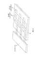
- FIG. 3illustrates a touch sensor 30 that may be utilized as touch sensor 10 of FIG. 1 .
- Touch sensor 30includes x-axis electrodes 32 , y-axis electrodes 34 , a substrate 35 , and a panel 36 .
- x-axis electrodes 32 and y-axis electrodes 34are electrodes in a self capacitance implementation (i.e., each x-axis electrode 32 and y-axis electrode 34 is capable of being driven and measured during the acquisition).
- x-axis electrodes 32are drive electrodes and y-axis electrodes 34 are sense electrodes in a mutual capacitance implementation.
- x-axis electrodes 32 and y-axis electrodes 34have a diamond pattern as illustrated in FIGS. 5A-5D below.
- panel 36is a transparent panel. In other embodiments, panel 36 is not transparent.
- substrate 35is sandwiched between x-axis electrodes 32 and y-axis electrodes 34 , and y-axis electrodes 34 are coupled to an underside of panel 36 with, for example, an adhesive.
- touch sensor 30includes any appropriate configuration and number of layers of electrodes and substrates. For example, some embodiments of touch sensor 30 include additional layers of sense electrodes 32 that run perpendicular (or any other appropriate angle) to y-axis electrodes 34 .
- x-axis electrodes 32 and y-axis electrodes 34are on the same layer in any appropriate pattern (e.g., a design in which x-axis electrodes 32 and y-axis electrodes 34 have interdigitated teeth).
- touch sensor 30determines the location of touch object 38 at least in part by using controller 12 to apply a pulsed a or alternating voltage to x-axis electrodes 32 , which induces a charge on y-axis electrodes 34 .
- touch sensor 30determines the location of touch object 38 at least in part by using controller 12 to apply a pulsed or alternating voltage to x-axis electrodes 32 and y-axis electrodes 34 .
- the change in capacitanceis sensed by the sense (i.e., receiving) electrodes and measured by controller 12 .
- the change in capacitanceis sensed by x-axis electrodes 32 and y-axis electrodes 34 and measured by controller 12 .
- controller 12determines the position of the touch or proximity within the touch-sensitive area(s) of touch sensor 30 .
- FIG. 4illustrates a self-capacitance embodiment of touch sensor 10 .
- touch sensor 10may include an array of electrodes of a single type that may each form a capacitive node.
- controller 12may measure the change in capacitance, for example, as a change in the amount of charge needed to raise the voltage at the capacitive node by a pre-determined amount.
- controller 12may determine the position of the touch or proximity within the touch-sensitive area(s) of touch sensor 10 .
- This disclosurecontemplates any suitable form of capacitive touch sensing, where appropriate.
- FIGS. 5A-5Dillustrate pseudo driven shield switch architectures 50 of touch sensor 10 of FIG. 1 for various self capacitance measuring techniques.
- FIGS. 5A and 5Dillustrate switch architectures 50 A and 50 D that utilize current source sensors.
- FIG. 5Billustrates a switch architecture 50 B that utilize capacitive sensors.
- FIG. 5Cillustrates a switch architecture 50 C that utilizes QTouch® sensors. While specific sensors are illustrated in FIGS. 5A-5D , other embodiments may utilize any appropriate sensor.
- Switch architectures 50 A- 50 D of FIGS. 5A-5Dinclude horizontal electrodes 52 , vertical electrodes 54 , sensors 56 (i.e., 56 A- 56 D), switches 58 (i.e., 58 A- 58 D), and one or more shield sensors 59 .
- Switches 58may be any appropriate switch and operate to electrically couple horizontal electrodes 52 and vertical electrodes 54 to sensors 56 and shield sensor 59 .
- switches 58 Aare operable to electrically couple some or all of horizontal electrodes 52 to sensors 56 A
- switches 58 Bare operable to electrically couple some or all of vertical electrodes 54 to sensors 56 B
- switches 58 Care operable to electrically couple horizontal electrodes 52 to shield sensor 59
- switches 58 Dare operable to electrically couple vertical electrodes 54 to shield sensor 59 .
- Horizontal electrodes 52 and vertical electrodes 54are any appropriate electrodes in any appropriate configuration.
- horizontal electrodes 52 and vertical electrodes 54are the x-axis 32 and y-axis 34 electrodes described above.
- horizontal electrodes 52 and vertical electrodes 54form a symmetrical pattern (i.e., the exposed area of horizontal electrodes 52 and vertical electrodes 54 are substantially equal).
- the pattern of horizontal electrodes 52 and vertical electrodes 54is a diamond pattern (as illustrated) or any appropriate clone of a diamond pattern.
- horizontal electrodes 52may not be exactly horizontal and vertical electrodes 54 may not be exactly vertical. Rather, horizontal electrodes 52 may be any appropriate angle to horizontal and vertical electrodes 54 may be any appropriate angle to vertical. This disclosure is not limited to the configuration and pattern of the illustrated horizontal electrodes 52 and vertical electrodes 54 . Instead, this disclosure anticipates any appropriate pattern, configuration, design, or arrangement of electrodes.
- Sensors 56 and shield sensor 59are any appropriate sensors to sense and/or measure capacitances from horizontal electrodes 52 and vertical electrodes 54 .
- sensors 56 and shield sensor 59may be current source sensors in some embodiments, as illustrated in FIGS. 5A and 5D .
- sensors 56 and shield sensor 59may be capacitive sensors in some embodiments, as illustrated in FIG. 5B .
- sensors 56 and shield sensor 59are communicatively coupled to or incorporated within controller 12 .
- sensors 56 and shield sensor 59may be channels of any appropriate microcontroller such as the QTouch® microcontroller, as illustrated in FIG. 5C , and may utilize any appropriate charge transfer technology.
- Such embodimentsmay include sample capacitors 57 , as illustrated in FIG. 5C .
- each sensor 56 A and 56 Bmay include an associated sample capacitor 57 (i.e., Cs) as illustrated
- shield sensor 59may include an associated shield sample capacitor 57 (i.e., Csh), as illustrated.
- the shield sample capacitor 57 of shield sensor 59may be a capacitor in the range of approximately 5 nF to 100 nF. Sample capacitors 57 are adjusted in such a way to produce identical or nearly identical voltages to horizontal electrodes 52 and vertical electrodes 54 during charge transfers.
- Switches 58may be any appropriate switch that may be selectively opened or closed in order to connect or disconnect two electrical nodes. In some embodiments, switches 58 are analog switches. In other embodiments, switches 58 are any other appropriate switch. In certain embodiments, switches 58 may be controlled by controller 12 .
- certain embodimentscombine hovering detection and proximity detection by utilizing switches 58 , sensors 56 , and shield sensor 59 to cause substantially equal voltages (e.g., voltages as illustrated in FIG. 6 ) to be present on non-measured electrodes 52 or 54 while capacitance measurements are performed on other electrodes 52 or 54 .
- hovering and proximity detectionshould be done by measuring self capacitance simultaneously on all rows and columns of a screen.
- parallel measurements of a whole screen for hovering detectionrequires individual capacitive sensing modules on each of the electrodes or each of the clusters of electrodes (where the proximity detection requires a single sensing module connected to all screen electrodes).
- the number of the individual sensing modules required for hovering detectionmay become too numerous, so hovering detection is typically done by sequentially scanning part of screen (e.g., first all rows and then all columns).
- Partial measurements of a screenmay create problems. For example, partial measurements may create an unwanted interaction between measured electrodes and non-measured electrodes. This interaction may affect the distribution of electrical field lines around the screen surface.
- the dielectrichas the ability to concentrate the field lines.
- embodiments of the disclosureattempt to cause identical or substantially identical voltages on both measured and non-measured electrodes (i.e., make non-measured electrodes equipotential to measured electrodes) while capacitance measurements are being performed.
- fast, high current output OpAmpsmay be used to drive all non-measured electrodes to the same voltage as the measured electrodes.
- Such solutionshowever, increase the power consumption of the chip and require large silicon areas.
- embodiments of the disclosure illustrated in FIGS. 5A-5Dcreate a pseudo driven shield by connecting all non-measured electrodes to one or more shield sensors 59 .
- all non-measured electrodesare connected to a single line that is coupled to a single shield sensor 59 . In other embodiments, all non-measured electrodes are connected to two or more shield sensor 59 using multiple lines.
- the pseudo driven shield architectureallows voltages on all non-measured electrodes to be equal or substantially equal to voltages of the measured electrodes.
- a current source methodis utilized to cause identical or substantially identical voltages (e.g., as illustrated in FIG. 6 ) on both measured and non-measured electrodes 52 and 54 while capacitance measurements are performed.
- shield sensor 59charges the shield (i.e., the non-measured electrodes 52 or 54 ) with current sources that are tuned to produce an identical charging curve as measured electrodes 52 or 54 .
- the sensitivity of the pseudo driven shieldis N times higher (when measuring charge) compared to the sensitivity of a single electrode, where N is the number of the electrodes connected to the shield (the sensitivity in the current sources method depends on the integrator gain multiplied by the ratio Cx/Cint and Cx in N times bigger).
- the voltage on the shieldis equal to the voltages of all other measured electrodes 52 or 54 .
- a current mirror methodis utilized to cause identical or substantially identical voltages on both measured and non-measured electrodes 52 and 54 while capacitance measurements are performed.
- shield sensor 59charges the shield and the measured electrodes 52 or 54 with limited currents that are tuned to produce an identical charging curve as measured electrodes 52 or 54 .
- current mirrorsare used to charge both a measured capacitor and an internal sampling capacitor as described in U.S. patent application Ser. No. 13/445,748, which is incorporated herein by reference. As a result, the voltage on the shield is equal to the voltages of all other measured electrodes 52 or 54 .
- FIG. 5Billustrates a current mirror method being utilized, any other appropriate method for causing identical or substantially identical voltages on both measured and non-measured electrodes 52 and 54 while capacitance measurements are performed may be utilized.
- a QTouch® methodis utilized to cause identical or substantially identical voltages on both measured and non-measured electrodes 52 and 54 while capacitance measurements are performed.
- QTouch®uses bursts to perform the capacitance measurements. For example, the number of pulses in the burst before the input flips is the measured signal itself.
- the shieldis connected to a shield sample capacitor 57 that has a value that produces identical voltages on non-measured electrodes 52 or 54 and the measured electrodes 52 or 54 during charge transfers. As a result, the voltage on the shield is equal to the voltages of all other measured electrodes 52 or 54 .
- FIGS. 5A-5Dillustrate particular measuring techniques
- other embodimentsmay utilize any other measuring technique in which shield voltages of the shield are equal or substantially equal to the voltages on the measured electrodes 52 or 54 .
- This disclosureanticipates using any appropriate measuring technique with the pseudo driven shield.
- screen measurements using the pseudo driven shield as illustrated in FIGS. 5A-5Dare done in two passes.
- all horizontal electrodes 52are connected to the individual sensors 56 and all vertical electrodes 54 are connected to shield sensor 59 .
- the measurements of all horizontal electrodes 52 and the shieldare then performed simultaneously.
- the unused horizontal electrodes 52may also be connected to shield sensor 59 .
- all vertical electrodes 54are connected to the individual sensors 56 and all horizontal electrodes 52 are connected to shield sensor 59 .
- the measurements of all vertical electrodes 54 and the shieldare then performed simultaneously.
- the unused vertical electrodes 54may also be connected to the shield.
- the signals measured from the shieldi.e., from shield sensor 59
- the signals measured from the shieldhave some specific features. First, it is detecting the object presence evenly across the area covered by the shield because all horizontal electrodes 52 or vertical electrodes 54 are connected together. This creates a virtual electrode with the dimensions of the screen (and half of the screen area). Second, it can detect the object presence from a long distance because the parallel measurements of the shield and the horizontal electrodes 52 or vertical electrodes 54 project the electrical field lines far away from the screen surface. This allows the proximity detection signal to be obtained without having to do an additional measuring cycle. This makes the signal from the shield ideal for proximity detection.
- FIG. 5Dillustrates an example embodiment in which there are not enough sensors 56 to connect to each of the electrodes.
- the measurementsmay be split into two or more measurements.
- the vertical electrodes 54may first be split into two or more groups: GROUP 1 and GROUP 2.
- horizontal electrodes 52may be split into GROUP 3 and GROUP 4.
- GROUP 1 measurementsare taken by connecting GROUP 1 electrodes to sensors 56 and connecting all other electrodes to the shield (i.e., to shield sensor 59 ).
- GROUP 2 measurementsare taken by connecting GROUP 2 electrodes to sensors 56 and connecting all other electrodes to the shield.
- GROUP 3 measurementsare taken by connecting GROUP 3 electrodes to sensors 56 and connecting all other electrodes to the shield.
- GROUP 4 measurementsare taken by connecting GROUP 4 electrodes to sensors 56 and connecting all other electrodes to the shield.
- FIG. 6illustrates example voltages that may be present on the electrodes of FIGS. 5A , 5 B, and 5 D.
- embodiments of the disclosurestrive to keep voltages on measured lines (i.e., electrodes; top graph) and the voltage on the shield (bottom graph) identical or substantially identical.
- the voltagesincrease linearly, which are specific to current source methods.
- the voltagesinclude bumps where the voltages go from increasing linearly to horizontal—another feature specific to current source methods.
- FIG. 6is not directly applicable to QTouch® embodiments (e.g., FIG. 5C ) in which the voltage rises on steps during the burst and is not increasing linearly.
- FIGS. 7-9illustrate effects of water or moisture on touch sensors and how embodiments of the pseudo driven shield may mitigate such effects.
- One benefit of using embodiments of the pseudo driven shieldis an increased immunity of the screen against moisture and water film.
- Moisture or water film on the surface of a touch screencreates a conductive film which works as distributed RC array as illustrated in FIG. 7 .
- the presence of the conductive film on the surfacecan create false touches or false hover detections if a grounded object is in contact with this film, as illustrated in FIG. 8 .
- FIG. 8Through the water film the presence of the object is affecting the measuring electrode via Cx 1 and the water film distributed R and C (capacitive coupling between measuring electrode and the water film on top of this electrode).
- some current Iwfwill flow through Cx 1 .
- FIG. 10illustrates an example method 1000 that is used in certain embodiments to perform proximity and hovering detection using the pseudo driven shields of FIGS. 5A-5D .
- Method 1000begins in step 1010 where a first, second, third, and fourth plurality of switches of a touch sensor are selectively controlled.
- the touch sensoris touch sensor 10 described above.
- the switches of step 1010are controlled by controller 12 .
- the first plurality of switchesmay refer to all or a portion of switches 58 A
- the second plurality of switchesmay refer to all or a portion of switches 58 B
- the third plurality of switchesmay refer to all or a portion of switches 58 C
- the fourth plurality of switchesmay refer to all or a portion of switches 58 D.
- the first, second, third, and fourth plurality of switchesmay refer to any other appropriate group of switches.
- the switches of step 1010may be analog switches.
- the first plurality of switches of step 1010are operable to electrically couple a plurality of first electrodes of the touch sensor to a plurality of sensors
- the second plurality of switchesare operable to electrically couple a plurality of second electrodes of the touch sensor to the plurality of sensors
- the third plurality of switchesare operable to electrically couple the plurality of first electrodes to a shield sensor
- the fourth plurality of switchesare operable to electrically couple the plurality of second electrodes to the shield sensor.
- the plurality of sensorsmay refer to sensors 56 described above (e.g., all or a portion of sensors 56 A or sensors 56 B).
- the first electrodesmay refer to all or a portion of horizontal electrodes 52 and the second electrodes may refer to all or a portion of vertical electrodes 54 , or vice versa.
- the first electrodesare horizontal (i.e., x-axis) electrodes and the second electrodes are vertical (i.e., y-axis) electrodes, or vice versa.
- the first and second electrodeshave exposed areas in a diamond pattern or any clone of a diamond pattern.
- the shield sensor of step 1010may refer to one or more shield sensors 59 above.
- the shield sensoris a shield current source sensor, and electrodes coupled to the shield current source sensor are charged with current sources that are tuned to produce a similar charging curve as electrodes of the touch sensor that are not coupled to the shield current source sensor.
- the shield sensoris a shield current source sensor, and the plurality of first and second electrodes are charged with limited currents that are tuned to produce identical charging.
- the shield sensoris QTouch® channel with a sampling capacitor that has a value that produces identical voltages on electrodes coupled to the shield sensor as voltages on electrodes of the touch sensor not coupled to the shield sensor.
- controlling the first, second, third, and fourth plurality of switches of step 1010includes closing at least a portion of the first plurality of switches to couple each of at least a portion of the plurality of first electrodes to a particular one of the plurality of sensors, opening the second plurality of switches to decouple (i.e., disconnect) the plurality of second electrodes from the plurality of sensors, opening the third plurality of switches to decouple the plurality of first electrodes from the shield sensor, and closing the fourth plurality of switches to couple all electrodes of the plurality of second electrodes to the shield sensor.
- controlling the first, second, third, and fourth plurality of switches of step 1010includes opening the first plurality of switches to decouple the plurality of first electrodes from the plurality of sensors, closing at least a portion of the second plurality of switches to couple each of at least a portion of the plurality of second electrodes to a particular one of the plurality of sensors, closing the third plurality of switches to couple all electrodes of the plurality of first electrodes to the shield sensor, and opening the fourth plurality of switches to decouple the second electrodes from the shield sensor.
- controlling the first, second, third, and fourth plurality of switches of step 1010includes coupling each of the electrodes that are to be measured to one of the plurality of sensors and coupling the remaining electrodes (i.e., the non-measured electrodes) to the shield (e.g., one or more shield sensors 59 ).
- substantially equal voltagesare caused to be present on the plurality of first and second electrodes of step 1010 .
- a variable amount of chargeis injected into each electrode in such a way to cause equal or substantially equal voltages on all electrodes (when there is no touch/hovering object on the surface).
- current sourcesare used and the currents are adjusted to produce an identical or substantially identically charging profile for each electrode.
- the electrodesare charged to the same voltage and then the charge is integrated.
- an amount of chargeis injected into each of the electrodes which produces equal or substantially equal voltages on all electrodes.
- the charging currentsare adjusted in such a way to produce equal voltage profiles (but the amount of the injected charge may be different for each electrode because each electrode has a different capacitance).
- step 1030capacitances of certain electrodes of step 1010 are measured with the plurality of sensors while the first and second electrodes are at substantially equal voltages.
- step 1030includes performing simultaneous hovering and proximity detection by causing substantially equal voltages to be present on the first and second electrodes while measuring capacitances of non-measured electrodes using the shield sensor and measuring capacitances of measured electrodes using the plurality of sensors.
- the capacitances of step 1030are measured using one or more of sensors 56 and/or one or more shield sensors 59 .
- measuring the capacitances of step 1030includes measuring capacitances of one or more of the first electrodes using the plurality of sensors, measuring a single capacitance for all of the second electrodes using the shield sensor, measuring capacitances of one or more of the second electrodes using the plurality of sensors, or measuring a single capacitance for all of the first electrodes using the shield sensor.
- example embodiments disclosed hereinprovide a touch sensor that is capable of simultaneously performing hover and proximity detection using a pseudo driven shield.
- devices utilizing embodiments of the disclosed touch sensormay have improved efficiency and power management and therefore may consume less power.
- embodiments of the disclosureprovide numerous enhancements over typical touch sensors.
- a computer-readable storage mediumencompasses one or more non-transitory, tangible computer-readable storage media possessing structure.
- a computer-readable storage mediummay include a semiconductor-based or other integrated circuit (IC) (such, as for example, a field-programmable gate array (FPGA) or an application-specific IC (ASIC)), a hard disk, an HDD, a hybrid hard drive (HHD), an optical disc, an optical disc drive (ODD), a magneto-optical disc, a magneto-optical drive, a floppy disk, a floppy disk drive (FDD), magnetic tape, a holographic storage medium, a solid-state drive (SSD), a RAM-drive, a SECURE DIGITAL card, a SECURE DIGITAL drive, or another suitable computer-readable storage medium or a combination of two or more of these, where appropriate.
- ICsemiconductor-based or other integrated circuit
- HDDhigh-programmable gate array
- HHDhybrid hard drive
- ODDoptical disc drive
- reference to a computer-readable storage mediumexcludes any medium that is not eligible for patent protection under 35 U.S.C. ⁇ 101.
- reference to a computer-readable storage mediumexcludes transitory forms of signal transmission (such as a propagating electrical or electromagnetic signal per se) to the extent that they are not eligible for patent protection under 35 U.S.C. ⁇ 101.
- a computer-readable non-transitory storage mediummay be volatile, non-volatile, or a combination of volatile and non-volatile, where appropriate.
- references in the appended claims to an apparatus or system or a component of an apparatus or system being adapted to, arranged to, capable of, configured to, enabled to, operable to, or operative to perform a particular functionencompasses that apparatus, system, component, whether or not it or that particular function is activated, turned on, or unlocked, as long as that apparatus, system, or component is so adapted, arranged, capable, configured, enabled, operable, or operative.
Landscapes
- Engineering & Computer Science (AREA)
- General Engineering & Computer Science (AREA)
- Theoretical Computer Science (AREA)
- Human Computer Interaction (AREA)
- Physics & Mathematics (AREA)
- General Physics & Mathematics (AREA)
- Electronic Switches (AREA)
- Position Input By Displaying (AREA)
Abstract
Description
- This disclosure generally relates to touch sensors.
- A touch sensor detects the presence and location of a touch or the proximity of an object (such as a user's finger) within a touch-sensitive area of the touch sensor overlaid, for example, on a display screen. In a touch-sensitive-display application, the touch sensor enables a user to interact directly with what is displayed on the screen, rather than indirectly with a mouse or touchpad. A touch sensor may be attached to or provided as part of a desktop computer, laptop computer, tablet computer, personal digital assistant (PDA), smartphone, satellite navigation device, portable media player, portable game console, kiosk computer, point-of-sale device, or other suitable device. A control panel on a household or other appliance may include a touch sensor.
- There are different types of touch sensors, such as (for example) resistive touch screens, surface acoustic wave touch screens, capacitive touch screens, infrared touch screens, and optical touch screens. Herein, reference to a touch sensor encompasses a touch screen, and vice versa, where appropriate. A capacitive touch screen may include an insulator coated with a substantially transparent conductor in a particular pattern. When an object touches or comes within proximity of the surface of the capacitive touch screen, a change in capacitance occurs within the touch screen at the location of the touch or proximity. A controller processes the change in capacitance to determine the touch position(s) on the touch screen.
FIG. 1 illustrates an example touch sensor, according to certain embodiments;FIG. 2 illustrates an example device that utilizes the touch sensor ofFIG. 1 , according to certain embodiments;FIG. 3 illustrates an example embodiment of the touch sensor ofFIG. 1 , according to certain embodiments;FIG. 4 illustrates another example embodiment of the touch sensor ofFIG. 1 , according to certain embodiments;FIGS. 5A-5D illustrate pseudo driven shield switch architectures of the touch sensor ofFIG. 1 , according to certain embodiments;FIG. 6 illustrates example voltages present on the electrodes ofFIGS. 5A ,5B, and5D), according to certain embodiments;FIGS. 7-9 illustrate effects of water or moisture on touch sensors, according to certain embodiments; andFIG. 10 illustrates an example method that is used in certain embodiments to perform proximity and hovering detection using the pseudo driven shields ofFIGS. 5A-5D , according to certain embodiments.- Proximity detection for capacitive touch screens involves the ability to detect the presence of an external object in the near vicinity to the screen surface without determining the exact spatial position of the object. For example, the typical detection range may vary from 40 mm to 200 mm and more. Hovering detection, however, involves determining the spatial position of the object relative to the surface before the object touches the surface. A typical range for hovering detection may be between 10 mm and 30 mm.
- Information from proximity and hovering detection may be used by a touch-sensitive device such as a smart phone or tablet computer in many different ways. For example, proximity event information may be utilized to wake up the device, for changing the behavior of the system, for illuminating the screen, for showing alerts, and the like. As another example, hovering event information may be utilized to determine where a person's finger is located related to the surface of the screen. Proximity and hovering detection, however, typically involves separate measurement processes and/or cycles by a touch sensor.
- The teachings of the disclosure recognize that it would be desirable to combine proximity and hovering detection by a touch sensor. Certain embodiments of the disclosure utilize a pseudo driven shield to cause a substantially equal voltage to be present on non-measured electrodes of a touch sensor as the voltage that is present on electrodes of the touch sensor that are being measured. As a result, the touch sensor is able to simultaneously detect proximity and hovering of objects relative to the surface of the screen of the touch sensor.
FIGS. 1 through 10 below illustrate a touch sensor of a touch-sensitive device that utilizes a pseudo driven shield to simultaneously perform proximity and hovering detection. FIG. 1 illustrates anexample touch sensor 10 with anexample controller 12. Herein, reference to a touch sensor may encompass a touch screen, and vice versa, where appropriate. Touchsensor 10 andcontroller 12 detect the presence and location of a touch or the proximity of an object within a touch-sensitive area oftouch sensor 10. Herein, reference to a touch sensor encompasses both the touch sensor and its controller, where appropriate. Similarly, reference to a controller encompasses both the controller and its touch sensor, where appropriate.Touch sensor 10 includes one or more touch-sensitive areas, where appropriate.Touch sensor 10 includes an array of touch electrodes (i.e., drive and/or sense electrodes) disposed on a substrate, which in some embodiments is a dielectric material.- In certain embodiments, one or more portions of the substrate of
touch sensor 10 are made of polyethylene terephthalate (PET) or another suitable material. This disclosure contemplates any suitable substrate with any suitable portions made of any suitable material. In particular embodiments, the drive or sense electrodes intouch sensor 10 are made of indium tin oxide (ITO) in whole or in part. In particular embodiments, the drive or sense electrodes intouch sensor 10 are made of fine lines of metal or other conductive material. As an example and not by way of limitation, one or more portions of the conductive material are copper or copper-based and have a thickness of approximately 5 μm or less and a width of approximately 10 μm or less. As another example, one or more portions of the conductive material are silver or silver-based and similarly have a thickness of approximately 5 μm or less and a width of approximately 10 μm or less. This disclosure contemplates any suitable electrodes made of any suitable material. - In certain embodiments,
touch sensor 10 implements a capacitive form of touch sensing. In a mutual-capacitance implementation,touch sensor 10 includes an array of drive and sense electrodes forming an array of capacitive nodes. In certain embodiments, a drive electrode and a sense electrode form a capacitive node. The drive and sense electrodes forming the capacitive node come near each other, but do not make electrical contact with each other. Instead, the drive and sense electrodes are capacitively coupled to each other across a gap between them. A pulsed or alternating voltage applied to the drive electrode (i.e., by controller12) induces a charge on the sense electrode, and the amount of charge induced is susceptible to external influence (such as a touch or the proximity of an object). When an object touches or comes within proximity of the capacitive node, a change in capacitance occurs at the capacitive node andcontroller 12 measures the change in capacitance. By measuring changes in capacitance throughout the array,controller 12 determines the position of the touch or proximity within the touch-sensitive area(s) oftouch sensor 10. - In particular embodiments, one or more drive electrodes together form a drive line running horizontally or vertically or in any suitable orientation. Similarly, one or more sense electrodes together form a sense line running horizontally or vertically or in any suitable orientation. In particular embodiments, drive lines run substantially perpendicular to sense lines. Herein, reference to a drive line encompasses one or more drive electrodes making up the drive line, and vice versa, where appropriate. Similarly, reference to a sense line encompasses one or more sense electrodes making up the sense line, and vice versa, where appropriate.
- In certain embodiments,
touch sensor 10 has a single-layer mutual capacitance configuration, with drive and sense electrodes disposed in a pattern on one side of a substrate. In such a configuration, a pair of drive and sense electrodes capacitively coupled to each other across a space between them forms a capacitive node. In a configuration for a self-capacitance implementation, as illustrated inFIG. 4 , electrodes of only a single type (e.g. sense) are disposed in a pattern on the substrate. Although this disclosure describes particular configurations of particular electrodes forming particular nodes, this disclosure contemplates any suitable configuration of any suitable electrodes forming any suitable nodes. Moreover, this disclosure contemplates any suitable electrodes disposed on any suitable number of any suitable substrates in any suitable patterns. - As described above, a change in capacitance at a capacitive node of
touch sensor 10 may indicate a touch or proximity input at the position of the capacitive node.Controller 12 is operable to detect and process the change in capacitance to determine the presence and location of the touch or proximity input. Certain embodiments ifcontroller 12 communicate information about the touch or proximity input to one or more other components (such one or more central processing units (CPUs) or digital signal processors (DSPs)) of a device that includestouch sensor 10 andcontroller 12, which may respond to the touch or proximity input by initiating a function of the device (or an application running on the device) associated with it. Although this disclosure describes a particular controller having particular functionality with respect to a particular device and a particular touch sensor, this disclosure contemplates any suitable controller having any suitable functionality with respect to any suitable device and any suitable touch sensor. - In certain embodiments,
controller 12 is one or more integrated circuits (ICs)—such as for example general-purpose microprocessors, microcontrollers, programmable logic devices or arrays, and application-specific ICs (ASICs). In some embodiments,controller 12 is coupled to a flexible printed circuit (FPC) bonded to the substrate oftouch sensor 10, as described below. In some mutual capacitance embodiments,controller 12 includes a processor unit, a drive unit, a sense unit, and a storage unit. The drive unit supplies drive signals to the drive electrodes oftouch sensor 10. The sense unit senses charge at the capacitive nodes oftouch sensor 10 and provides measurement signals to the processor unit representing capacitances at the capacitive nodes. The processor unit controls the supply of drive signals to the drive electrodes by the drive unit and process measurement signals from the sense unit to detect and process the presence and location of a touch or proximity input within the touch-sensitive area(s) oftouch sensor 10. The processor unit also tracks changes in the position of a touch or proximity input within the touch-sensitive area(s) oftouch sensor 10. The storage unit, which includes one or more memory devices, stores programming for execution by the processor unit, including programming for controlling the drive unit to supply drive signals to the drive electrodes, programming for processing measurement signals from the sense unit, and other suitable programming, where appropriate. In self capacitance embodiments,controller 12 is operable to both drive and measure electrodes that are each individually a sense and drive electrode. Although this disclosure describes a particular controller having a particular implementation with particular components, this disclosure contemplates any suitable controller having any suitable implementation with any suitable components. Tracks 14 of conductive material disposed on the substrate oftouch sensor 10 couple the drive or sense electrodes oftouch sensor 10 toconnection pads 16, also disposed on the substrate oftouch sensor 10. As described below,connection pads 16 facilitate coupling oftracks 14 tocontroller 12. In certain embodiments, tracks14 extend into or around (e.g. at the edges of) the touch-sensitive area(s) oftouch sensor 10.Particular tracks 14 provide drive connections for couplingcontroller 12 to drive electrodes oftouch sensor 10, through which the drive unit ofcontroller 12 supplies drive signals to the drive electrodes.Other tracks 14 provide sense connections for couplingcontroller 12 to sense electrodes oftouch sensor 10, through which the sense unit ofcontroller 12 senses charge at the capacitive nodes oftouch sensor 10. In certain embodiments, tracks14 are made of fine lines of metal or other conductive material. As an example and not by way of limitation, the conductive material oftracks 14 is copper or copper-based and have a width of approximately 100 μm or less. As another example, the conductive material oftracks 14 is silver or silver-based and have a width of approximately 100 μm or less. In particular embodiments, tracks14 are made of ITO in whole or in part in addition or as an alternative to fine lines of metal or other conductive material. Although this disclosure describes particular tracks made of particular materials with particular widths, this disclosure contemplates any suitable tracks made of any suitable materials with any suitable widths. In addition totracks 14, certain embodiments oftouch sensor 10 include one or more ground lines terminating at a ground connector (similar to a connection pad16) at an edge of the substrate of touch sensor10 (similar to tracks14).- In certain embodiments,
connection pads 16 are located along one or more edges of the substrate, outside the touch-sensitive area(s) oftouch sensor 10. As described above,controller 12 is on an FPC in certain embodiments. In some embodiments,connection pads 16 are made of the same material astracks 14 and are bonded to the FPC using an anisotropic conductive film (ACF). In certain embodiments,connection 18 includes conductive lines on theFPC coupling controller 12 toconnection pads 16, inturn coupling controller 12 totracks 14 and to the drive or sense electrodes oftouch sensor 10. In another embodiment, connection pads160 are inserted into an electro-mechanical connector (such as a zero insertion force wire-to-board connector); in this embodiment, connection180 does not need to include an FPC. This disclosure contemplates anysuitable connection 18 betweencontroller 12 andtouch sensor 10. FIG. 2 illustrates anexample device 20 that utilizestouch sensor 10 ofFIG. 1 .Device 20 includes any personal digital assistant, cellular telephone, smartphone, tablet computer, and the like. For example, a certain embodiment ofdevice 20 is a smartphone that includes a touchscreen display22 (e.g., screen) occupying a significant portion of the largest surface of the device. In certain embodiments, the large size oftouchscreen display 22 enables thetouchscreen display 22 to present a wide variety of data, including a keyboard, a numeric keypad, program or application icons, and various other interfaces as desired. In certain embodiments, a user interacts withdevice 20 by touchingtouchscreen display 22 with a stylus, a finger, or any other appropriate object in order to interact with device20 (i.e., select a program for execution or to type a letter on a keyboard displayed on the touchscreen display22). In certain embodiments, a user interacts withdevice 20 using multiple touches to perform various operations, such as to zoom in or zoom out when viewing a document or image.FIG. 3 illustrates atouch sensor 30 that may be utilized astouch sensor 10 ofFIG. 1 .Touch sensor 30 includesx-axis electrodes 32, y-axis electrodes 34, asubstrate 35, and apanel 36. In some embodiments,x-axis electrodes 32 and y-axis electrodes 34 are electrodes in a self capacitance implementation (i.e., eachx-axis electrode 32 and y-axis electrode 34 is capable of being driven and measured during the acquisition). In some embodiments,x-axis electrodes 32 are drive electrodes and y-axis electrodes 34 are sense electrodes in a mutual capacitance implementation. In some embodiments,x-axis electrodes 32 and y-axis electrodes 34 have a diamond pattern as illustrated inFIGS. 5A-5D below.- In some embodiments,
panel 36 is a transparent panel. In other embodiments,panel 36 is not transparent. In some embodiments,substrate 35 is sandwiched betweenx-axis electrodes 32 and y-axis electrodes 34, and y-axis electrodes 34 are coupled to an underside ofpanel 36 with, for example, an adhesive. In other embodiments,touch sensor 30 includes any appropriate configuration and number of layers of electrodes and substrates. For example, some embodiments oftouch sensor 30 include additional layers ofsense electrodes 32 that run perpendicular (or any other appropriate angle) to y-axis electrodes 34. In some embodiments,x-axis electrodes 32 and y-axis electrodes 34 are on the same layer in any appropriate pattern (e.g., a design in which x-axiselectrodes 32 and y-axis electrodes 34 have interdigitated teeth). - In certain mutual capacitance embodiments,
touch sensor 30 determines the location oftouch object 38 at least in part by usingcontroller 12 to apply a pulsed a or alternating voltage tox-axis electrodes 32, which induces a charge on y-axis electrodes 34. In certain self capacitance embodiments,touch sensor 30 determines the location oftouch object 38 at least in part by usingcontroller 12 to apply a pulsed or alternating voltage tox-axis electrodes 32 and y-axis electrodes 34. When touch object38 touches or comes within proximity of an active area oftouch sensor 30, a change in capacitance may occur, as depicted by electric field lines39 inFIG. 3 . In mutual capacitance embodiments, the change in capacitance is sensed by the sense (i.e., receiving) electrodes and measured bycontroller 12. In self capacitance embodiments, the change in capacitance is sensed byx-axis electrodes 32 and y-axis electrodes 34 and measured bycontroller 12. By measuring changes in capacitance throughout an array ofx-axis electrodes 32 and y-axis electrodes 34,controller 12 determines the position of the touch or proximity within the touch-sensitive area(s) oftouch sensor 30. FIG. 4 illustrates a self-capacitance embodiment oftouch sensor 10. In a self-capacitance implementation,touch sensor 10 may include an array of electrodes of a single type that may each form a capacitive node. When an object touches or comes within proximity of the capacitive node, a change in self-capacitance may occur at the capacitive node andcontroller 12 may measure the change in capacitance, for example, as a change in the amount of charge needed to raise the voltage at the capacitive node by a pre-determined amount. As with a mutual-capacitance implementation, by measuring changes in capacitance throughout the array,controller 12 may determine the position of the touch or proximity within the touch-sensitive area(s) oftouch sensor 10. This disclosure contemplates any suitable form of capacitive touch sensing, where appropriate.FIGS. 5A-5D illustrate pseudo driven shield switch architectures50 oftouch sensor 10 ofFIG. 1 for various self capacitance measuring techniques.FIGS. 5A and 5D illustrateswitch architectures 50A and50D that utilize current source sensors.FIG. 5B illustrates a switch architecture50B that utilize capacitive sensors.FIG. 5C illustrates a switch architecture50C that utilizes QTouch® sensors. While specific sensors are illustrated inFIGS. 5A-5D , other embodiments may utilize any appropriate sensor.Switch architectures 50A-50D ofFIGS. 5A-5D includehorizontal electrodes 52,vertical electrodes 54, sensors56 (i.e.,56A-56D), switches58 (i.e.,58A-58D), and one or more shield sensors59.Switches 58 may be any appropriate switch and operate to electrically couplehorizontal electrodes 52 andvertical electrodes 54 tosensors 56 and shield sensor59. For example, switches58A are operable to electrically couple some or all ofhorizontal electrodes 52 tosensors 56A, switches58B are operable to electrically couple some or all ofvertical electrodes 54 to sensors56B, switches58C are operable to electrically couplehorizontal electrodes 52 to shield sensor59, and switches58D are operable to electrically couplevertical electrodes 54 to shield sensor59.Horizontal electrodes 52 andvertical electrodes 54 are any appropriate electrodes in any appropriate configuration. In some embodiments,horizontal electrodes 52 andvertical electrodes 54 are the x-axis32 and y-axis 34 electrodes described above. In certain embodiments,horizontal electrodes 52 andvertical electrodes 54 form a symmetrical pattern (i.e., the exposed area ofhorizontal electrodes 52 andvertical electrodes 54 are substantially equal). In some embodiments, the pattern ofhorizontal electrodes 52 andvertical electrodes 54 is a diamond pattern (as illustrated) or any appropriate clone of a diamond pattern. In certain embodiments,horizontal electrodes 52 may not be exactly horizontal andvertical electrodes 54 may not be exactly vertical. Rather,horizontal electrodes 52 may be any appropriate angle to horizontal andvertical electrodes 54 may be any appropriate angle to vertical. This disclosure is not limited to the configuration and pattern of the illustratedhorizontal electrodes 52 andvertical electrodes 54. Instead, this disclosure anticipates any appropriate pattern, configuration, design, or arrangement of electrodes.Sensors 56 and shield sensor59 are any appropriate sensors to sense and/or measure capacitances fromhorizontal electrodes 52 andvertical electrodes 54. For example,sensors 56 and shield sensor59 may be current source sensors in some embodiments, as illustrated inFIGS. 5A and 5D . In such embodiments, current sources are used to inject a fixed amount of charge into the measured capacitance by sourcing or sinking a constant current for a fixed amount of time (Q=I*t). The change in the capacitance will result in change in the voltage at the end of the charge injection. As another example,sensors 56 and shield sensor59 may be capacitive sensors in some embodiments, as illustrated inFIG. 5B . In some embodiments,sensors 56 and shield sensor59 are communicatively coupled to or incorporated withincontroller 12.- In some embodiments,
sensors 56 and shield sensor59 may be channels of any appropriate microcontroller such as the QTouch® microcontroller, as illustrated inFIG. 5C , and may utilize any appropriate charge transfer technology. Such embodiments may includesample capacitors 57, as illustrated inFIG. 5C . For example, eachsensor 56A and56B may include an associated sample capacitor57 (i.e., Cs) as illustrated, and shield sensor59 may include an associated shield sample capacitor57 (i.e., Csh), as illustrated. In some embodiments, theshield sample capacitor 57 of shield sensor59 may be a capacitor in the range of approximately 5 nF to 100 nF.Sample capacitors 57 are adjusted in such a way to produce identical or nearly identical voltages tohorizontal electrodes 52 andvertical electrodes 54 during charge transfers. Switches 58 may be any appropriate switch that may be selectively opened or closed in order to connect or disconnect two electrical nodes. In some embodiments, switches58 are analog switches. In other embodiments, switches58 are any other appropriate switch. In certain embodiments, switches58 may be controlled bycontroller 12.- In operation, certain embodiments combine hovering detection and proximity detection by utilizing
switches 58,sensors 56, and shield sensor59 to cause substantially equal voltages (e.g., voltages as illustrated inFIG. 6 ) to be present onnon-measured electrodes other electrodes - Partial measurements of a screen, however, may create problems. For example, partial measurements may create an unwanted interaction between measured electrodes and non-measured electrodes. This interaction may affect the distribution of electrical field lines around the screen surface. One solution—holding the non-measured electrodes to a fixed voltage (e.g., GND or Vdd)—has negative effects on the measurements. For example, holding the non-measured electrodes to a fixed voltage reduces the hovering range and increase stray capacitance to GND on the boundary electrodes (i.e., measured electrodes immediately next to non-measured electrodes). As another example, if some of the electrodes are connected to a fixed voltage, the dielectric has the ability to concentrate the field lines. The result is that more of the field lines are trapped inside the dielectric and few lines can escape the dielectric in order to interact with the objects in close vicinity to the surface. In short, the combination of increased capacitive loading plus the change in the electrical field lines trajectory causes decreased ability to detect far away objects.
- To remove the interaction between measured electrodes and non-measured electrodes, embodiments of the disclosure attempt to cause identical or substantially identical voltages on both measured and non-measured electrodes (i.e., make non-measured electrodes equipotential to measured electrodes) while capacitance measurements are being performed. In typical solutions, fast, high current output OpAmps may be used to drive all non-measured electrodes to the same voltage as the measured electrodes. Such solutions, however, increase the power consumption of the chip and require large silicon areas. Instead of using OpAmps for driving the non-measured electrodes, embodiments of the disclosure illustrated in
FIGS. 5A-5D create a pseudo driven shield by connecting all non-measured electrodes to one or more shield sensors59. In some embodiments, all non-measured electrodes are connected to a single line that is coupled to a single shield sensor59. In other embodiments, all non-measured electrodes are connected to two or more shield sensor59 using multiple lines. The pseudo driven shield architecture allows voltages on all non-measured electrodes to be equal or substantially equal to voltages of the measured electrodes. - In
FIGS. 5A and 5D , a current source method is utilized to cause identical or substantially identical voltages (e.g., as illustrated inFIG. 6 ) on both measured andnon-measured electrodes non-measured electrodes 52 or54) with current sources that are tuned to produce an identical charging curve as measuredelectrodes electrodes - In
FIG. 5B , a current mirror method is utilized to cause identical or substantially identical voltages on both measured andnon-measured electrodes electrodes electrodes electrodes FIG. 5B illustrates a current mirror method being utilized, any other appropriate method for causing identical or substantially identical voltages on both measured andnon-measured electrodes - In
FIG. 5C , a QTouch® method is utilized to cause identical or substantially identical voltages on both measured andnon-measured electrodes FIG. 5C , the shield is connected to ashield sample capacitor 57 that has a value that produces identical voltages onnon-measured electrodes electrodes electrodes - While
FIGS. 5A-5D illustrate particular measuring techniques, other embodiments may utilize any other measuring technique in which shield voltages of the shield are equal or substantially equal to the voltages on the measuredelectrodes - In some embodiments, screen measurements using the pseudo driven shield as illustrated in
FIGS. 5A-5D are done in two passes. For example, in the first pass, allhorizontal electrodes 52 are connected to theindividual sensors 56 and allvertical electrodes 54 are connected to shield sensor59. The measurements of allhorizontal electrodes 52 and the shield are then performed simultaneously. In some embodiments, if the silicon is not able to support measurements on allhorizontal electrodes 52, the unusedhorizontal electrodes 52 may also be connected to shield sensor59. In the second pass, allvertical electrodes 54 are connected to theindividual sensors 56 and allhorizontal electrodes 52 are connected to shield sensor59. The measurements of allvertical electrodes 54 and the shield are then performed simultaneously. In some embodiments, if the silicon is not able to support measurements on allvertical electrodes 54, the unusedvertical electrodes 54 may also be connected to the shield. - When measurements using the pseudo driven shield are done in two passes as described above, the signals measured from the shield (i.e., from shield sensor59) have some specific features. First, it is detecting the object presence evenly across the area covered by the shield because all
horizontal electrodes 52 orvertical electrodes 54 are connected together. This creates a virtual electrode with the dimensions of the screen (and half of the screen area). Second, it can detect the object presence from a long distance because the parallel measurements of the shield and thehorizontal electrodes 52 orvertical electrodes 54 project the electrical field lines far away from the screen surface. This allows the proximity detection signal to be obtained without having to do an additional measuring cycle. This makes the signal from the shield ideal for proximity detection. - In certain embodiments, only a portion of
horizontal electrodes 52 orvertical electrodes 54 may be measured in a measurement cycle. For example,FIG. 5D illustrates an example embodiment in which there are notenough sensors 56 to connect to each of the electrodes. In this case, the measurements may be split into two or more measurements. For example, thevertical electrodes 54 may first be split into two or more groups: GROUP 1 andGROUP 2. Similarly,horizontal electrodes 52 may be split intoGROUP 3 andGROUP 4. Next, GROUP 1 measurements are taken by connecting GROUP 1 electrodes tosensors 56 and connecting all other electrodes to the shield (i.e., to shield sensor59). Next,GROUP 2 measurements are taken by connectingGROUP 2 electrodes tosensors 56 and connecting all other electrodes to the shield. Next,GROUP 3 measurements are taken by connectingGROUP 3 electrodes tosensors 56 and connecting all other electrodes to the shield. Finally,GROUP 4 measurements are taken by connectingGROUP 4 electrodes tosensors 56 and connecting all other electrodes to the shield. FIG. 6 illustrates example voltages that may be present on the electrodes ofFIGS. 5A ,5B, and5D. In general, embodiments of the disclosure strive to keep voltages on measured lines (i.e., electrodes; top graph) and the voltage on the shield (bottom graph) identical or substantially identical. In the illustrated embodiment, the voltages increase linearly, which are specific to current source methods. In addition, the voltages include bumps where the voltages go from increasing linearly to horizontal—another feature specific to current source methods. It should be noted thatFIG. 6 is not directly applicable to QTouch® embodiments (e.g.,FIG. 5C ) in which the voltage rises on steps during the burst and is not increasing linearly.FIGS. 7-9 illustrate effects of water or moisture on touch sensors and how embodiments of the pseudo driven shield may mitigate such effects. One benefit of using embodiments of the pseudo driven shield is an increased immunity of the screen against moisture and water film. Moisture or water film on the surface of a touch screen creates a conductive film which works as distributed RC array as illustrated inFIG. 7 . The presence of the conductive film on the surface can create false touches or false hover detections if a grounded object is in contact with this film, as illustrated inFIG. 8 . Through the water film the presence of the object is affecting the measuring electrode via Cx1 and the water film distributed R and C (capacitive coupling between measuring electrode and the water film on top of this electrode). As illustrated inFIG. 8 , some current Iwf will flow through Cx1.- When using a shield electrode as illustrated in
FIG. 9 , a large portion of the water film effect is cancelled through the capacitance Csh (the capacitive coupling between the shield electrode and the water film). The shield has a shunting effect and prevents the propagation of the capacitance changes introduced by the grounded object through the water film. As illustrated inFIG. 9 , the same current Iwf fromFIG. 8 is flowing but through capacitance Csh to the shield electrode. Although the currents continue to flow (Iwf) and may be the same strength, they are changed from where they flow. Until the active electrode and the shield are substantially equipotential, substantially no currents can flow between them. The result is that no currents are flowing through Cx1 but rather the current Iwf is flowing through Csh. FIG. 10 illustrates anexample method 1000 that is used in certain embodiments to perform proximity and hovering detection using the pseudo driven shields ofFIGS. 5A-5D .Method 1000 begins instep 1010 where a first, second, third, and fourth plurality of switches of a touch sensor are selectively controlled. In some embodiments, the touch sensor istouch sensor 10 described above. In some embodiments, the switches ofstep 1010 are controlled bycontroller 12. In some embodiments, the first plurality of switches may refer to all or a portion of switches58A, the second plurality of switches may refer to all or a portion ofswitches 58B, the third plurality of switches may refer to all or a portion ofswitches 58C, and the fourth plurality of switches may refer to all or a portion ofswitches 58D. In other embodiments, the first, second, third, and fourth plurality of switches may refer to any other appropriate group of switches. In some embodiments, the switches ofstep 1010 may be analog switches.- In some embodiments, the first plurality of switches of
step 1010 are operable to electrically couple a plurality of first electrodes of the touch sensor to a plurality of sensors, the second plurality of switches are operable to electrically couple a plurality of second electrodes of the touch sensor to the plurality of sensors, the third plurality of switches are operable to electrically couple the plurality of first electrodes to a shield sensor, and the fourth plurality of switches are operable to electrically couple the plurality of second electrodes to the shield sensor. In some embodiments, the plurality of sensors may refer tosensors 56 described above (e.g., all or a portion ofsensors 56A or sensors56B). In some embodiments, the first electrodes may refer to all or a portion ofhorizontal electrodes 52 and the second electrodes may refer to all or a portion ofvertical electrodes 54, or vice versa. In some embodiments, the first electrodes are horizontal (i.e., x-axis) electrodes and the second electrodes are vertical (i.e., y-axis) electrodes, or vice versa. In certain embodiments, the first and second electrodes have exposed areas in a diamond pattern or any clone of a diamond pattern. - In some embodiments, the shield sensor of
step 1010 may refer to one or more shield sensors59 above. In certain embodiments, the shield sensor is a shield current source sensor, and electrodes coupled to the shield current source sensor are charged with current sources that are tuned to produce a similar charging curve as electrodes of the touch sensor that are not coupled to the shield current source sensor. In some embodiments, the shield sensor is a shield current source sensor, and the plurality of first and second electrodes are charged with limited currents that are tuned to produce identical charging. In some embodiments, the shield sensor is QTouch® channel with a sampling capacitor that has a value that produces identical voltages on electrodes coupled to the shield sensor as voltages on electrodes of the touch sensor not coupled to the shield sensor. - In some embodiments, controlling the first, second, third, and fourth plurality of switches of
step 1010 includes closing at least a portion of the first plurality of switches to couple each of at least a portion of the plurality of first electrodes to a particular one of the plurality of sensors, opening the second plurality of switches to decouple (i.e., disconnect) the plurality of second electrodes from the plurality of sensors, opening the third plurality of switches to decouple the plurality of first electrodes from the shield sensor, and closing the fourth plurality of switches to couple all electrodes of the plurality of second electrodes to the shield sensor. In some embodiments, controlling the first, second, third, and fourth plurality of switches ofstep 1010 includes opening the first plurality of switches to decouple the plurality of first electrodes from the plurality of sensors, closing at least a portion of the second plurality of switches to couple each of at least a portion of the plurality of second electrodes to a particular one of the plurality of sensors, closing the third plurality of switches to couple all electrodes of the plurality of first electrodes to the shield sensor, and opening the fourth plurality of switches to decouple the second electrodes from the shield sensor. In general, controlling the first, second, third, and fourth plurality of switches ofstep 1010 includes coupling each of the electrodes that are to be measured to one of the plurality of sensors and coupling the remaining electrodes (i.e., the non-measured electrodes) to the shield (e.g., one or more shield sensors59). - In
step 1020, substantially equal voltages are caused to be present on the plurality of first and second electrodes ofstep 1010. In general, a variable amount of charge is injected into each electrode in such a way to cause equal or substantially equal voltages on all electrodes (when there is no touch/hovering object on the surface). In some embodiments, current sources are used and the currents are adjusted to produce an identical or substantially identically charging profile for each electrode. In embodiments where integration is used, the electrodes are charged to the same voltage and then the charge is integrated. In some embodiments, an amount of charge is injected into each of the electrodes which produces equal or substantially equal voltages on all electrodes. If current sources are used, the charging currents are adjusted in such a way to produce equal voltage profiles (but the amount of the injected charge may be different for each electrode because each electrode has a different capacitance). In some embodiments, the charge Q is found by the equation: Q=CU (where C is the capacitance, U is the voltage). In general, embodiments strive to keep U constant across all electrodes. In some embodiments, unless C is different for each electrode, Q is adjusted to keep U constant across all electrodes. - In
step 1030, capacitances of certain electrodes ofstep 1010 are measured with the plurality of sensors while the first and second electrodes are at substantially equal voltages. In certain embodiments,step 1030 includes performing simultaneous hovering and proximity detection by causing substantially equal voltages to be present on the first and second electrodes while measuring capacitances of non-measured electrodes using the shield sensor and measuring capacitances of measured electrodes using the plurality of sensors. In some embodiments, the capacitances ofstep 1030 are measured using one or more ofsensors 56 and/or one or more shield sensors59. In some embodiments, measuring the capacitances ofstep 1030 includes measuring capacitances of one or more of the first electrodes using the plurality of sensors, measuring a single capacitance for all of the second electrodes using the shield sensor, measuring capacitances of one or more of the second electrodes using the plurality of sensors, or measuring a single capacitance for all of the first electrodes using the shield sensor. - Accordingly, example embodiments disclosed herein provide a touch sensor that is capable of simultaneously performing hover and proximity detection using a pseudo driven shield. As a result, devices utilizing embodiments of the disclosed touch sensor may have improved efficiency and power management and therefore may consume less power. Accordingly, embodiments of the disclosure provide numerous enhancements over typical touch sensors.
- Although the preceding examples given here generally rely on self capacitance or mutual capacitance to operate, other embodiments of the invention will use other technologies, including other capacitance measures, resistance, or other such sense technologies.
- Herein, reference to a computer-readable storage medium encompasses one or more non-transitory, tangible computer-readable storage media possessing structure. As an example and not by way of limitation, a computer-readable storage medium may include a semiconductor-based or other integrated circuit (IC) (such, as for example, a field-programmable gate array (FPGA) or an application-specific IC (ASIC)), a hard disk, an HDD, a hybrid hard drive (HHD), an optical disc, an optical disc drive (ODD), a magneto-optical disc, a magneto-optical drive, a floppy disk, a floppy disk drive (FDD), magnetic tape, a holographic storage medium, a solid-state drive (SSD), a RAM-drive, a SECURE DIGITAL card, a SECURE DIGITAL drive, or another suitable computer-readable storage medium or a combination of two or more of these, where appropriate. Herein, reference to a computer-readable storage medium excludes any medium that is not eligible for patent protection under 35 U.S.C. §101. Herein, reference to a computer-readable storage medium excludes transitory forms of signal transmission (such as a propagating electrical or electromagnetic signal per se) to the extent that they are not eligible for patent protection under 35 U.S.C. §101. A computer-readable non-transitory storage medium may be volatile, non-volatile, or a combination of volatile and non-volatile, where appropriate.
- Herein, “or” is inclusive and not exclusive, unless expressly indicated otherwise or indicated otherwise by context. Therefore, herein, “A or B” means “A, B, or both.” unless expressly indicated otherwise or indicated otherwise by context. Moreover, “and” is both joint and several, unless expressly indicated otherwise or indicated otherwise by context. Therefore, herein, “A and B” means “A and B, jointly or severally,” unless expressly indicated otherwise or indicated otherwise by context.
- This disclosure encompasses all changes, substitutions, variations, alterations, and modifications to the example embodiments herein that a person having ordinary skill in the art would comprehend. For example, while the illustrated embodiments of the pseudo driven shield depict connecting
horizontal electrodes 52 andvertical electrodes 54 to a single shield sensor59 to form the shield, other embodiments may connect the shield to multiple shield sensors59. Moreover, reference in the appended claims to an apparatus or system or a component of an apparatus or system being adapted to, arranged to, capable of, configured to, enabled to, operable to, or operative to perform a particular function encompasses that apparatus, system, component, whether or not it or that particular function is activated, turned on, or unlocked, as long as that apparatus, system, or component is so adapted, arranged, capable, configured, enabled, operable, or operative.
Claims (20)
Priority Applications (4)
| Application Number | Priority Date | Filing Date | Title |
|---|---|---|---|
| US13/930,754US9612677B2 (en) | 2013-06-28 | 2013-06-28 | Pseudo driven shield |
| DE102014212094.2ADE102014212094A1 (en) | 2013-06-28 | 2014-06-24 | Pseudo-driven shielding |
| US15/477,866US10031632B2 (en) | 2013-06-28 | 2017-04-03 | Pseudo driven shield |
| US16/042,872US20190004629A1 (en) | 2013-06-28 | 2018-07-23 | Pseudo Driven Shield |
Applications Claiming Priority (1)
| Application Number | Priority Date | Filing Date | Title |
|---|---|---|---|
| US13/930,754US9612677B2 (en) | 2013-06-28 | 2013-06-28 | Pseudo driven shield |
Related Child Applications (1)
| Application Number | Title | Priority Date | Filing Date |
|---|---|---|---|
| US15/477,866ContinuationUS10031632B2 (en) | 2013-06-28 | 2017-04-03 | Pseudo driven shield |
Publications (2)
| Publication Number | Publication Date |
|---|---|
| US20150002448A1true US20150002448A1 (en) | 2015-01-01 |
| US9612677B2 US9612677B2 (en) | 2017-04-04 |
Family
ID=52017583
Family Applications (3)
| Application Number | Title | Priority Date | Filing Date |
|---|---|---|---|
| US13/930,754Expired - Fee RelatedUS9612677B2 (en) | 2013-06-28 | 2013-06-28 | Pseudo driven shield |
| US15/477,866Expired - Fee RelatedUS10031632B2 (en) | 2013-06-28 | 2017-04-03 | Pseudo driven shield |
| US16/042,872AbandonedUS20190004629A1 (en) | 2013-06-28 | 2018-07-23 | Pseudo Driven Shield |
Family Applications After (2)
| Application Number | Title | Priority Date | Filing Date |
|---|---|---|---|
| US15/477,866Expired - Fee RelatedUS10031632B2 (en) | 2013-06-28 | 2017-04-03 | Pseudo driven shield |
| US16/042,872AbandonedUS20190004629A1 (en) | 2013-06-28 | 2018-07-23 | Pseudo Driven Shield |
Country Status (2)
| Country | Link |
|---|---|
| US (3) | US9612677B2 (en) |
| DE (1) | DE102014212094A1 (en) |
Cited By (31)
| Publication number | Priority date | Publication date | Assignee | Title |
|---|---|---|---|---|
| US20160154507A1 (en)* | 2014-12-01 | 2016-06-02 | Cypress Semiconductor Corporation | Systems, methods, and devices for touch event and hover event detection |
| US20160349898A1 (en)* | 2015-05-28 | 2016-12-01 | Novatek Microelectronics Corp. | Touch Control Module for Touch Device and Related Touch Control Method |
| US9582131B2 (en) | 2009-06-29 | 2017-02-28 | Apple Inc. | Touch sensor panel design |
| US20170090615A1 (en)* | 2015-09-30 | 2017-03-30 | Synaptics Incorporated | Two-dimensional absolute capacitance sensing using electrode guarding techniques |
| US20170277341A1 (en)* | 2016-03-23 | 2017-09-28 | Samsung Display Co., Ltd. | Method and apparatus for multi-sensing |
| US20170285804A1 (en)* | 2014-09-22 | 2017-10-05 | Apple Inc. | Ungrounded user signal compensation for pixelated self-capacitance touch sensor panel |
| US9874975B2 (en) | 2012-04-16 | 2018-01-23 | Apple Inc. | Reconstruction of original touch image from differential touch image |
| US9880655B2 (en) | 2014-09-02 | 2018-01-30 | Apple Inc. | Method of disambiguating water from a finger touch on a touch sensor panel |
| US9886141B2 (en)* | 2013-08-16 | 2018-02-06 | Apple Inc. | Mutual and self capacitance touch measurements in touch panel |
| US9996175B2 (en) | 2009-02-02 | 2018-06-12 | Apple Inc. | Switching circuitry for touch sensitive display |
| US10001888B2 (en) | 2009-04-10 | 2018-06-19 | Apple Inc. | Touch sensor panel design |
| WO2018119788A1 (en)* | 2016-12-27 | 2018-07-05 | 武汉华星光电技术有限公司 | Array substrate having embedded touch structure, and display panel |
| US20180307368A1 (en)* | 2017-04-20 | 2018-10-25 | Japan Display Inc. | Display device |
| US10289251B2 (en) | 2014-06-27 | 2019-05-14 | Apple Inc. | Reducing floating ground effects in pixelated self-capacitance touch screens |
| US10365773B2 (en) | 2015-09-30 | 2019-07-30 | Apple Inc. | Flexible scan plan using coarse mutual capacitance and fully-guarded measurements |
| US10386965B2 (en) | 2017-04-20 | 2019-08-20 | Apple Inc. | Finger tracking in wet environment |
| US10437365B2 (en) | 2017-10-11 | 2019-10-08 | Pixart Imaging Inc. | Driver integrated circuit of touch panel and associated driving method |
| US10444918B2 (en) | 2016-09-06 | 2019-10-15 | Apple Inc. | Back of cover touch sensors |
| US10474288B2 (en) | 2015-05-28 | 2019-11-12 | Novatek Microelectronics Corp. | Touch control method for touch device |
| US10488992B2 (en) | 2015-03-10 | 2019-11-26 | Apple Inc. | Multi-chip touch architecture for scalability |
| EP3121695B1 (en)* | 2015-07-20 | 2020-05-27 | LG Display Co., Ltd. | Fingerprint sensor integrated type touch screen device |
| US10712867B2 (en) | 2014-10-27 | 2020-07-14 | Apple Inc. | Pixelated self-capacitance water rejection |
| US10795488B2 (en) | 2015-02-02 | 2020-10-06 | Apple Inc. | Flexible self-capacitance and mutual capacitance touch sensing system architecture |
| TWI709897B (en)* | 2018-05-31 | 2020-11-11 | 李尚禮 | Detecting method of touch device and detecting module thereof |
| US10936120B2 (en) | 2014-05-22 | 2021-03-02 | Apple Inc. | Panel bootstraping architectures for in-cell self-capacitance |
| US11157109B1 (en)* | 2019-09-06 | 2021-10-26 | Apple Inc. | Touch sensing with water rejection |
| US11221697B2 (en) | 2013-08-28 | 2022-01-11 | Apple Inc. | Capacitive touch panel for sensing mechanical inputs to a device |
| US11294503B2 (en) | 2008-01-04 | 2022-04-05 | Apple Inc. | Sensor baseline offset adjustment for a subset of sensor output values |
| US20220206657A1 (en)* | 2020-12-24 | 2022-06-30 | Shanghai Tianma Micro-electronics Co., Ltd. | Detection device and display unit |
| US11422689B1 (en)* | 2018-08-09 | 2022-08-23 | Apple Inc. | Detecting touch user interface on a display under partial wet conditions |
| US11662867B1 (en) | 2020-05-30 | 2023-05-30 | Apple Inc. | Hover detection on a touch sensor panel |
Families Citing this family (2)
| Publication number | Priority date | Publication date | Assignee | Title |
|---|---|---|---|---|
| US11429224B2 (en)* | 2021-01-06 | 2022-08-30 | Rockwell Collins, Inc. | Eliminating interconnect induced inaccuracies and reducing scan time using a high granularity resistive touch screen |
| CN115167699A (en)* | 2022-06-09 | 2022-10-11 | 武汉华星光电半导体显示技术有限公司 | Touch substrate and display panel |
Citations (5)
| Publication number | Priority date | Publication date | Assignee | Title |
|---|---|---|---|---|
| US20090027068A1 (en)* | 2007-07-26 | 2009-01-29 | Qrg Limited | Proximity Sensor |
| US20100007628A1 (en)* | 2008-07-09 | 2010-01-14 | Takuya Eriguchi | Screen Input-Type Image Display System |
| US20110181549A1 (en)* | 2007-01-03 | 2011-07-28 | Steve Porter Hotelling | Double-sided touch-sensitive panel with shield and drive combined layer |
| US20140152621A1 (en)* | 2011-11-11 | 2014-06-05 | Panasonic Corporation | Touch-panel device |
| US20140218334A1 (en)* | 2011-06-24 | 2014-08-07 | Junichi Shibata | Input device using detection of both capacitance and pressure, and capacitance-system hybrid touch panel equipped with pressure-sensitive function |
Family Cites Families (24)
| Publication number | Priority date | Publication date | Assignee | Title |
|---|---|---|---|---|
| US7663607B2 (en) | 2004-05-06 | 2010-02-16 | Apple Inc. | Multipoint touchscreen |
| EP1746488A2 (en) | 2005-07-21 | 2007-01-24 | TPO Displays Corp. | Electromagnetic digitizer sensor array structure |
| US8031174B2 (en) | 2007-01-03 | 2011-10-04 | Apple Inc. | Multi-touch surface stackup arrangement |
| US8049732B2 (en) | 2007-01-03 | 2011-11-01 | Apple Inc. | Front-end signal compensation |
| TW200842681A (en) | 2007-04-27 | 2008-11-01 | Tpk Touch Solutions Inc | Touch pattern structure of a capacitive touch panel |
| TW200844827A (en) | 2007-05-11 | 2008-11-16 | Sense Pad Tech Co Ltd | Transparent touch panel device |
| US8040326B2 (en) | 2007-06-13 | 2011-10-18 | Apple Inc. | Integrated in-plane switching display and touch sensor |
| JP4506785B2 (en) | 2007-06-14 | 2010-07-21 | エプソンイメージングデバイス株式会社 | Capacitive input device |
| KR20100100773A (en)* | 2007-10-04 | 2010-09-15 | 가부시키가이샤후지쿠라 | Capacitive proximity sensor and proximity detection method |
| KR101720919B1 (en) | 2008-02-28 | 2017-03-28 | 쓰리엠 이노베이티브 프로퍼티즈 컴파니 | Touch screen sensor |
| JP4720857B2 (en) | 2008-06-18 | 2011-07-13 | ソニー株式会社 | Capacitance type input device and display device with input function |
| KR101002308B1 (en)* | 2008-09-12 | 2010-12-17 | 엘지디스플레이 주식회사 | Liquid crystal display |
| US8115499B2 (en)* | 2009-05-22 | 2012-02-14 | Freescale Semiconductor, Inc. | Device with proximity detection capability |
| US9069405B2 (en)* | 2009-07-28 | 2015-06-30 | Cypress Semiconductor Corporation | Dynamic mode switching for fast touch response |
| US8031094B2 (en) | 2009-09-11 | 2011-10-04 | Apple Inc. | Touch controller with improved analog front end |
| TWI433016B (en)* | 2010-04-30 | 2014-04-01 | Elan Microelectronics Corp | The capacitive touch panel sensing unit, and a sensing circuit sensing method |
| US8717331B2 (en)* | 2010-08-24 | 2014-05-06 | Cypress Semiconductor Corporation | Reducing water influence on a touch-sensing device |
| US9866660B2 (en) | 2011-03-21 | 2018-01-09 | Apple Inc. | Electronic devices with concave displays |
| WO2012129247A2 (en) | 2011-03-21 | 2012-09-27 | Apple Inc. | Electronic devices with flexible displays |
| US8934228B2 (en) | 2011-03-21 | 2015-01-13 | Apple Inc. | Display-based speaker structures for electronic devices |
| US8816977B2 (en) | 2011-03-21 | 2014-08-26 | Apple Inc. | Electronic devices with flexible displays |
| US9178970B2 (en) | 2011-03-21 | 2015-11-03 | Apple Inc. | Electronic devices with convex displays |
| US8665236B2 (en) | 2011-09-26 | 2014-03-04 | Apple Inc. | Electronic device with wrap around display |
| US8723824B2 (en) | 2011-09-27 | 2014-05-13 | Apple Inc. | Electronic devices with sidewall displays |
- 2013
- 2013-06-28USUS13/930,754patent/US9612677B2/ennot_activeExpired - Fee Related
- 2014
- 2014-06-24DEDE102014212094.2Apatent/DE102014212094A1/ennot_activeWithdrawn
- 2017
- 2017-04-03USUS15/477,866patent/US10031632B2/ennot_activeExpired - Fee Related
- 2018
- 2018-07-23USUS16/042,872patent/US20190004629A1/ennot_activeAbandoned
Patent Citations (5)
| Publication number | Priority date | Publication date | Assignee | Title |
|---|---|---|---|---|
| US20110181549A1 (en)* | 2007-01-03 | 2011-07-28 | Steve Porter Hotelling | Double-sided touch-sensitive panel with shield and drive combined layer |
| US20090027068A1 (en)* | 2007-07-26 | 2009-01-29 | Qrg Limited | Proximity Sensor |
| US20100007628A1 (en)* | 2008-07-09 | 2010-01-14 | Takuya Eriguchi | Screen Input-Type Image Display System |
| US20140218334A1 (en)* | 2011-06-24 | 2014-08-07 | Junichi Shibata | Input device using detection of both capacitance and pressure, and capacitance-system hybrid touch panel equipped with pressure-sensitive function |
| US20140152621A1 (en)* | 2011-11-11 | 2014-06-05 | Panasonic Corporation | Touch-panel device |
Cited By (55)
| Publication number | Priority date | Publication date | Assignee | Title |
|---|---|---|---|---|
| US11294503B2 (en) | 2008-01-04 | 2022-04-05 | Apple Inc. | Sensor baseline offset adjustment for a subset of sensor output values |
| US9996175B2 (en) | 2009-02-02 | 2018-06-12 | Apple Inc. | Switching circuitry for touch sensitive display |
| US10001888B2 (en) | 2009-04-10 | 2018-06-19 | Apple Inc. | Touch sensor panel design |
| US9582131B2 (en) | 2009-06-29 | 2017-02-28 | Apple Inc. | Touch sensor panel design |
| US9874975B2 (en) | 2012-04-16 | 2018-01-23 | Apple Inc. | Reconstruction of original touch image from differential touch image |
| US9886141B2 (en)* | 2013-08-16 | 2018-02-06 | Apple Inc. | Mutual and self capacitance touch measurements in touch panel |
| US12008178B2 (en) | 2013-08-28 | 2024-06-11 | Apple Inc. | Capacitive touch panel for sensing mechanical inputs to a device |
| US11556190B2 (en) | 2013-08-28 | 2023-01-17 | Apple Inc. | Capacitive touch panel for sensing mechanical inputs to a device |
| US11221697B2 (en) | 2013-08-28 | 2022-01-11 | Apple Inc. | Capacitive touch panel for sensing mechanical inputs to a device |
| US11740715B2 (en) | 2013-08-28 | 2023-08-29 | Apple Inc. | Capacitive touch panel for sensing mechanical inputs to a device |
| US12436629B2 (en) | 2013-08-28 | 2025-10-07 | Apple Inc. | Capacitive touch panel for sensing mechanical inputs to a device |
| US10936120B2 (en) | 2014-05-22 | 2021-03-02 | Apple Inc. | Panel bootstraping architectures for in-cell self-capacitance |
| US10289251B2 (en) | 2014-06-27 | 2019-05-14 | Apple Inc. | Reducing floating ground effects in pixelated self-capacitance touch screens |
| US9880655B2 (en) | 2014-09-02 | 2018-01-30 | Apple Inc. | Method of disambiguating water from a finger touch on a touch sensor panel |
| US10705658B2 (en)* | 2014-09-22 | 2020-07-07 | Apple Inc. | Ungrounded user signal compensation for pixelated self-capacitance touch sensor panel |
| US11625124B2 (en) | 2014-09-22 | 2023-04-11 | Apple Inc. | Ungrounded user signal compensation for pixelated self-capacitance touch sensor panel |
| US20170285804A1 (en)* | 2014-09-22 | 2017-10-05 | Apple Inc. | Ungrounded user signal compensation for pixelated self-capacitance touch sensor panel |
| US10712867B2 (en) | 2014-10-27 | 2020-07-14 | Apple Inc. | Pixelated self-capacitance water rejection |
| US11561647B2 (en) | 2014-10-27 | 2023-01-24 | Apple Inc. | Pixelated self-capacitance water rejection |
| WO2016089614A1 (en)* | 2014-12-01 | 2016-06-09 | Cypress Semiconductor Corporation | Systems, methods, and devices for touch event and hover event detection |
| US20160154507A1 (en)* | 2014-12-01 | 2016-06-02 | Cypress Semiconductor Corporation | Systems, methods, and devices for touch event and hover event detection |
| US10795488B2 (en) | 2015-02-02 | 2020-10-06 | Apple Inc. | Flexible self-capacitance and mutual capacitance touch sensing system architecture |
| US11353985B2 (en) | 2015-02-02 | 2022-06-07 | Apple Inc. | Flexible self-capacitance and mutual capacitance touch sensing system architecture |
| US12014003B2 (en) | 2015-02-02 | 2024-06-18 | Apple Inc. | Flexible self-capacitance and mutual capacitance touch sensing system architecture |
| US10488992B2 (en) | 2015-03-10 | 2019-11-26 | Apple Inc. | Multi-chip touch architecture for scalability |
| CN106201132A (en)* | 2015-05-28 | 2016-12-07 | 联咏科技股份有限公司 | Touch module for touch device and related touch method |
| US10474288B2 (en) | 2015-05-28 | 2019-11-12 | Novatek Microelectronics Corp. | Touch control method for touch device |
| US10852882B2 (en) | 2015-05-28 | 2020-12-01 | Novatek Microelectronics Corp. | Fingerprint sensing control method for fingerprint sensing device |
| US20160349898A1 (en)* | 2015-05-28 | 2016-12-01 | Novatek Microelectronics Corp. | Touch Control Module for Touch Device and Related Touch Control Method |
| US9996187B2 (en)* | 2015-05-28 | 2018-06-12 | Novatek Microelectronics Corp. | Touch control module for touch device and related touch control method |
| EP3121695B1 (en)* | 2015-07-20 | 2020-05-27 | LG Display Co., Ltd. | Fingerprint sensor integrated type touch screen device |
| US20170090615A1 (en)* | 2015-09-30 | 2017-03-30 | Synaptics Incorporated | Two-dimensional absolute capacitance sensing using electrode guarding techniques |
| US10365773B2 (en) | 2015-09-30 | 2019-07-30 | Apple Inc. | Flexible scan plan using coarse mutual capacitance and fully-guarded measurements |
| US10838536B2 (en)* | 2016-03-23 | 2020-11-17 | Samsung Display Co., Ltd. | Method and apparatus for multi-sensing |
| US20170277341A1 (en)* | 2016-03-23 | 2017-09-28 | Samsung Display Co., Ltd. | Method and apparatus for multi-sensing |
| US10444918B2 (en) | 2016-09-06 | 2019-10-15 | Apple Inc. | Back of cover touch sensors |
| US10203825B2 (en) | 2016-12-27 | 2019-02-12 | Wuhan China Star Optoelectronics Technology Co., Ltd | Array substrate having an embedded touch structure and display panel |
| WO2018119788A1 (en)* | 2016-12-27 | 2018-07-05 | 武汉华星光电技术有限公司 | Array substrate having embedded touch structure, and display panel |
| US20180307368A1 (en)* | 2017-04-20 | 2018-10-25 | Japan Display Inc. | Display device |
| US10664094B2 (en)* | 2017-04-20 | 2020-05-26 | Japan Display Inc. | Display device |
| US12044941B2 (en) | 2017-04-20 | 2024-07-23 | Japan Display Inc. | Display device |
| US11435628B2 (en) | 2017-04-20 | 2022-09-06 | Japan Display Inc. | Display device |
| US10386965B2 (en) | 2017-04-20 | 2019-08-20 | Apple Inc. | Finger tracking in wet environment |
| US11022851B2 (en) | 2017-04-20 | 2021-06-01 | Japan Display Inc. | Display device |
| US10642418B2 (en) | 2017-04-20 | 2020-05-05 | Apple Inc. | Finger tracking in wet environment |
| US11686983B2 (en) | 2017-04-20 | 2023-06-27 | Japan Display Inc. | Display device |
| US10437365B2 (en) | 2017-10-11 | 2019-10-08 | Pixart Imaging Inc. | Driver integrated circuit of touch panel and associated driving method |
| TWI709897B (en)* | 2018-05-31 | 2020-11-11 | 李尚禮 | Detecting method of touch device and detecting module thereof |
| US11733859B2 (en) | 2018-08-09 | 2023-08-22 | Apple Inc. | Detecting touch user interface on a display under partial wet conditions |
| US11422689B1 (en)* | 2018-08-09 | 2022-08-23 | Apple Inc. | Detecting touch user interface on a display under partial wet conditions |
| US11157109B1 (en)* | 2019-09-06 | 2021-10-26 | Apple Inc. | Touch sensing with water rejection |
| US12189899B2 (en) | 2019-09-06 | 2025-01-07 | Apple Inc. | Touch sensing with water rejection |
| US11662867B1 (en) | 2020-05-30 | 2023-05-30 | Apple Inc. | Hover detection on a touch sensor panel |
| US11907472B2 (en)* | 2020-12-24 | 2024-02-20 | Shanghai Tianma Micro-electronics Co., Ltd. | Detection device and display unit |
| US20220206657A1 (en)* | 2020-12-24 | 2022-06-30 | Shanghai Tianma Micro-electronics Co., Ltd. | Detection device and display unit |
Also Published As
| Publication number | Publication date |
|---|---|
| US10031632B2 (en) | 2018-07-24 |
| US20190004629A1 (en) | 2019-01-03 |
| US20170205916A1 (en) | 2017-07-20 |
| DE102014212094A1 (en) | 2014-12-31 |
| US9612677B2 (en) | 2017-04-04 |
Similar Documents
| Publication | Publication Date | Title |
|---|---|---|
| US10031632B2 (en) | Pseudo driven shield | |
| USRE48310E1 (en) | Active stylus with passive mutual measurements | |
| US9535545B2 (en) | Common mode noise suppression during hovering and proximity detection | |
| US8896327B2 (en) | Current mirror self-capacitance measurement | |
| TWI469022B (en) | Capacitive touchscreen system and method for detecting touch on capacitive touchscreen system | |
| US20130155000A1 (en) | Touch sensor with reduced anti-touch effects | |
| US20120182252A1 (en) | Differential Capacitive Touchscreen or Touch Panel | |
| US9921691B2 (en) | Burst-mode self-capacitance measurement with compensated capacitance | |
| US8847898B2 (en) | Signal-to-noise ratio in touch sensors | |
| US9389727B2 (en) | Method and system to determine when a device is being held | |
| US9098155B2 (en) | Self-capacitance measurement using compensation capacitor | |
| US11494037B2 (en) | Excitation voltages for touch sensors | |
| US10635253B2 (en) | Pattern of electrodes for a touch sensor | |
| US9081454B2 (en) | Touch sensor with capacitive voltage divider | |
| US9244559B2 (en) | Integrated pixel display and touch sensor | |
| US9081443B2 (en) | Shieldless touch sensor noise cancellation | |
| US9244570B2 (en) | System and method for reducing the effects of parasitic capacitances | |
| US9306560B2 (en) | Self-capacitance detection using trans-conductance reference | |
| US9417729B2 (en) | Charge compensation during touch sensing | |
| US20130141381A1 (en) | Surface Coverage Touch | |
| US9069423B2 (en) | Buffer-reference self-capacitance measurement |
Legal Events
| Date | Code | Title | Description |
|---|---|---|---|
| AS | Assignment | Owner name:ATMEL TECHNOLOGIES U.K. LIMITED, UNITED KINGDOM Free format text:ASSIGNMENT OF ASSIGNORS INTEREST;ASSIGNORS:BRUNET, SAMUEL;COLLINS, RICHARD PAUL;HRISTOV, LUBEN HRISTOV;AND OTHERS;SIGNING DATES FROM 20130626 TO 20130628;REEL/FRAME:030711/0539 Owner name:ATMEL CORPORATION, CALIFORNIA Free format text:ASSIGNMENT OF ASSIGNORS INTEREST;ASSIGNORS:MYREN, STEINAR;PEDERSEN, TROND JARLE;SIGNING DATES FROM 20130626 TO 20130627;REEL/FRAME:030711/0426 | |
| AS | Assignment | Owner name:ATMEL CORPORATION, CALIFORNIA Free format text:ASSIGNMENT OF ASSIGNORS INTEREST;ASSIGNOR:ATMEL TECHNOLOGIES U.K. LIMITED;REEL/FRAME:030807/0675 Effective date:20130703 | |
| AS | Assignment | Owner name:MORGAN STANLEY SENIOR FUNDING, INC. AS ADMINISTRATIVE AGENT, NEW YORK Free format text:PATENT SECURITY AGREEMENT;ASSIGNOR:ATMEL CORPORATION;REEL/FRAME:031912/0173 Effective date:20131206 Owner name:MORGAN STANLEY SENIOR FUNDING, INC. AS ADMINISTRAT Free format text:PATENT SECURITY AGREEMENT;ASSIGNOR:ATMEL CORPORATION;REEL/FRAME:031912/0173 Effective date:20131206 | |
| AS | Assignment | Owner name:ATMEL CORPORATION, CALIFORNIA Free format text:TERMINATION AND RELEASE OF SECURITY INTEREST IN PATENT COLLATERAL;ASSIGNOR:MORGAN STANLEY SENIOR FUNDING, INC.;REEL/FRAME:038376/0001 Effective date:20160404 | |
| AS | Assignment | Owner name:JPMORGAN CHASE BANK, N.A., AS ADMINISTRATIVE AGENT, ILLINOIS Free format text:SECURITY INTEREST;ASSIGNOR:ATMEL CORPORATION;REEL/FRAME:041715/0747 Effective date:20170208 Owner name:JPMORGAN CHASE BANK, N.A., AS ADMINISTRATIVE AGENT Free format text:SECURITY INTEREST;ASSIGNOR:ATMEL CORPORATION;REEL/FRAME:041715/0747 Effective date:20170208 | |
| STCF | Information on status: patent grant | Free format text:PATENTED CASE | |
| AS | Assignment | Owner name:JPMORGAN CHASE BANK, N.A., AS ADMINISTRATIVE AGENT, ILLINOIS Free format text:SECURITY INTEREST;ASSIGNORS:MICROCHIP TECHNOLOGY INCORPORATED;SILICON STORAGE TECHNOLOGY, INC.;ATMEL CORPORATION;AND OTHERS;REEL/FRAME:046426/0001 Effective date:20180529 Owner name:JPMORGAN CHASE BANK, N.A., AS ADMINISTRATIVE AGENT Free format text:SECURITY INTEREST;ASSIGNORS:MICROCHIP TECHNOLOGY INCORPORATED;SILICON STORAGE TECHNOLOGY, INC.;ATMEL CORPORATION;AND OTHERS;REEL/FRAME:046426/0001 Effective date:20180529 | |
| AS | Assignment | Owner name:WELLS FARGO BANK, NATIONAL ASSOCIATION, AS NOTES COLLATERAL AGENT, CALIFORNIA Free format text:SECURITY INTEREST;ASSIGNORS:MICROCHIP TECHNOLOGY INCORPORATED;SILICON STORAGE TECHNOLOGY, INC.;ATMEL CORPORATION;AND OTHERS;REEL/FRAME:047103/0206 Effective date:20180914 Owner name:WELLS FARGO BANK, NATIONAL ASSOCIATION, AS NOTES C Free format text:SECURITY INTEREST;ASSIGNORS:MICROCHIP TECHNOLOGY INCORPORATED;SILICON STORAGE TECHNOLOGY, INC.;ATMEL CORPORATION;AND OTHERS;REEL/FRAME:047103/0206 Effective date:20180914 | |
| AS | Assignment | Owner name:MICROCHIP TECHNOLOGY INCORPORATED, ARIZONA Free format text:RELEASE OF SECURITY INTEREST IN CERTAIN PATENT RIGHTS;ASSIGNOR:JPMORGAN CHASE BANK, N.A., AS ADMINISTRATIVE AGENT;REEL/FRAME:047976/0884 Effective date:20181221 Owner name:ATMEL CORPORATION, ARIZONA Free format text:RELEASE OF SECURITY INTEREST IN CERTAIN PATENT RIGHTS;ASSIGNOR:WELLS FARGO BANK, NATIONAL ASSOCIATION, AS NOTES COLLATERAL AGENT;REEL/FRAME:047976/0937 Effective date:20181221 Owner name:ATMEL CORPORATION, ARIZONA Free format text:RELEASE OF SECURITY INTEREST IN CERTAIN PATENT RIGHTS;ASSIGNOR:JPMORGAN CHASE BANK, N.A., AS ADMINISTRATIVE AGENT;REEL/FRAME:047976/0884 Effective date:20181221 Owner name:MICROCHIP TECHNOLOGY INCORPORATED, ARIZONA Free format text:RELEASE OF SECURITY INTEREST IN CERTAIN PATENT RIGHTS;ASSIGNOR:WELLS FARGO BANK, NATIONAL ASSOCIATION, AS NOTES COLLATERAL AGENT;REEL/FRAME:047976/0937 Effective date:20181221 | |
| AS | Assignment | Owner name:NEODRON LIMITED, IRELAND Free format text:ASSIGNMENT OF ASSIGNORS INTEREST;ASSIGNORS:MICROCHIP TECHNOLOGY INC.;ATMEL CORPORATION;MICROCHIP TECHNOLOGY GERMANY GMBH;REEL/FRAME:048259/0840 Effective date:20181221 | |
| MAFP | Maintenance fee payment | Free format text:PAYMENT OF MAINTENANCE FEE, 4TH YEAR, LARGE ENTITY (ORIGINAL EVENT CODE: M1551); ENTITY STATUS OF PATENT OWNER: LARGE ENTITY Year of fee payment:4 | |
| AS | Assignment | Owner name:MICROSEMI STORAGE SOLUTIONS, INC., ARIZONA Free format text:RELEASE BY SECURED PARTY;ASSIGNOR:JPMORGAN CHASE BANK, N.A., AS ADMINISTRATIVE AGENT;REEL/FRAME:059333/0222 Effective date:20220218 Owner name:MICROSEMI CORPORATION, ARIZONA Free format text:RELEASE BY SECURED PARTY;ASSIGNOR:JPMORGAN CHASE BANK, N.A., AS ADMINISTRATIVE AGENT;REEL/FRAME:059333/0222 Effective date:20220218 Owner name:ATMEL CORPORATION, ARIZONA Free format text:RELEASE BY SECURED PARTY;ASSIGNOR:JPMORGAN CHASE BANK, N.A., AS ADMINISTRATIVE AGENT;REEL/FRAME:059333/0222 Effective date:20220218 Owner name:SILICON STORAGE TECHNOLOGY, INC., ARIZONA Free format text:RELEASE BY SECURED PARTY;ASSIGNOR:JPMORGAN CHASE BANK, N.A., AS ADMINISTRATIVE AGENT;REEL/FRAME:059333/0222 Effective date:20220218 Owner name:MICROCHIP TECHNOLOGY INCORPORATED, ARIZONA Free format text:RELEASE BY SECURED PARTY;ASSIGNOR:JPMORGAN CHASE BANK, N.A., AS ADMINISTRATIVE AGENT;REEL/FRAME:059333/0222 Effective date:20220218 | |
| AS | Assignment | Owner name:ATMEL CORPORATION, ARIZONA Free format text:RELEASE BY SECURED PARTY;ASSIGNOR:JPMORGAN CHASE BANK, N.A., AS ADMINISTRATIVE AGENT;REEL/FRAME:059262/0105 Effective date:20220218 | |
| AS | Assignment | Owner name:MICROSEMI STORAGE SOLUTIONS, INC., ARIZONA Free format text:RELEASE BY SECURED PARTY;ASSIGNOR:WELLS FARGO BANK, NATIONAL ASSOCIATION, AS NOTES COLLATERAL AGENT;REEL/FRAME:059358/0001 Effective date:20220228 Owner name:MICROSEMI CORPORATION, ARIZONA Free format text:RELEASE BY SECURED PARTY;ASSIGNOR:WELLS FARGO BANK, NATIONAL ASSOCIATION, AS NOTES COLLATERAL AGENT;REEL/FRAME:059358/0001 Effective date:20220228 Owner name:ATMEL CORPORATION, ARIZONA Free format text:RELEASE BY SECURED PARTY;ASSIGNOR:WELLS FARGO BANK, NATIONAL ASSOCIATION, AS NOTES COLLATERAL AGENT;REEL/FRAME:059358/0001 Effective date:20220228 Owner name:SILICON STORAGE TECHNOLOGY, INC., ARIZONA Free format text:RELEASE BY SECURED PARTY;ASSIGNOR:WELLS FARGO BANK, NATIONAL ASSOCIATION, AS NOTES COLLATERAL AGENT;REEL/FRAME:059358/0001 Effective date:20220228 Owner name:MICROCHIP TECHNOLOGY INCORPORATED, ARIZONA Free format text:RELEASE BY SECURED PARTY;ASSIGNOR:WELLS FARGO BANK, NATIONAL ASSOCIATION, AS NOTES COLLATERAL AGENT;REEL/FRAME:059358/0001 Effective date:20220228 | |
| FEPP | Fee payment procedure | Free format text:MAINTENANCE FEE REMINDER MAILED (ORIGINAL EVENT CODE: REM.); ENTITY STATUS OF PATENT OWNER: LARGE ENTITY | |
| LAPS | Lapse for failure to pay maintenance fees | Free format text:PATENT EXPIRED FOR FAILURE TO PAY MAINTENANCE FEES (ORIGINAL EVENT CODE: EXP.); ENTITY STATUS OF PATENT OWNER: LARGE ENTITY | |
| STCH | Information on status: patent discontinuation | Free format text:PATENT EXPIRED DUE TO NONPAYMENT OF MAINTENANCE FEES UNDER 37 CFR 1.362 | |
| FP | Lapsed due to failure to pay maintenance fee | Effective date:20250404 |