US20150001612A1 - Non-volatile memory (nvm) and high voltage transistor integration - Google Patents
Non-volatile memory (nvm) and high voltage transistor integrationDownload PDFInfo
- Publication number
- US20150001612A1 US20150001612A1US13/928,666US201313928666AUS2015001612A1US 20150001612 A1US20150001612 A1US 20150001612A1US 201313928666 AUS201313928666 AUS 201313928666AUS 2015001612 A1US2015001612 A1US 2015001612A1
- Authority
- US
- United States
- Prior art keywords
- region
- high voltage
- charge storage
- nvm
- logic
- Prior art date
- Legal status (The legal status is an assumption and is not a legal conclusion. Google has not performed a legal analysis and makes no representation as to the accuracy of the status listed.)
- Granted
Links
Images


Classifications
- H01L29/792—
- H—ELECTRICITY
- H10—SEMICONDUCTOR DEVICES; ELECTRIC SOLID-STATE DEVICES NOT OTHERWISE PROVIDED FOR
- H10D—INORGANIC ELECTRIC SEMICONDUCTOR DEVICES
- H10D30/00—Field-effect transistors [FET]
- H10D30/60—Insulated-gate field-effect transistors [IGFET]
- H10D30/69—IGFETs having charge trapping gate insulators, e.g. MNOS transistors
- H01L29/66833—
- H—ELECTRICITY
- H10—SEMICONDUCTOR DEVICES; ELECTRIC SOLID-STATE DEVICES NOT OTHERWISE PROVIDED FOR
- H10B—ELECTRONIC MEMORY DEVICES
- H10B41/00—Electrically erasable-and-programmable ROM [EEPROM] devices comprising floating gates
- H10B41/40—Electrically erasable-and-programmable ROM [EEPROM] devices comprising floating gates characterised by the peripheral circuit region
- H10B41/41—Electrically erasable-and-programmable ROM [EEPROM] devices comprising floating gates characterised by the peripheral circuit region of a memory region comprising a cell select transistor, e.g. NAND
- H—ELECTRICITY
- H10—SEMICONDUCTOR DEVICES; ELECTRIC SOLID-STATE DEVICES NOT OTHERWISE PROVIDED FOR
- H10B—ELECTRONIC MEMORY DEVICES
- H10B41/00—Electrically erasable-and-programmable ROM [EEPROM] devices comprising floating gates
- H10B41/40—Electrically erasable-and-programmable ROM [EEPROM] devices comprising floating gates characterised by the peripheral circuit region
- H10B41/42—Simultaneous manufacture of periphery and memory cells
- H10B41/49—Simultaneous manufacture of periphery and memory cells comprising different types of peripheral transistor
- H—ELECTRICITY
- H10—SEMICONDUCTOR DEVICES; ELECTRIC SOLID-STATE DEVICES NOT OTHERWISE PROVIDED FOR
- H10D—INORGANIC ELECTRIC SEMICONDUCTOR DEVICES
- H10D30/00—Field-effect transistors [FET]
- H10D30/01—Manufacture or treatment
- H10D30/021—Manufacture or treatment of FETs having insulated gates [IGFET]
- H10D30/0411—Manufacture or treatment of FETs having insulated gates [IGFET] of FETs having floating gates
- H—ELECTRICITY
- H10—SEMICONDUCTOR DEVICES; ELECTRIC SOLID-STATE DEVICES NOT OTHERWISE PROVIDED FOR
- H10D—INORGANIC ELECTRIC SEMICONDUCTOR DEVICES
- H10D30/00—Field-effect transistors [FET]
- H10D30/01—Manufacture or treatment
- H10D30/021—Manufacture or treatment of FETs having insulated gates [IGFET]
- H10D30/0413—Manufacture or treatment of FETs having insulated gates [IGFET] of FETs having charge-trapping gate insulators, e.g. MNOS transistors
- H—ELECTRICITY
- H10—SEMICONDUCTOR DEVICES; ELECTRIC SOLID-STATE DEVICES NOT OTHERWISE PROVIDED FOR
- H10D—INORGANIC ELECTRIC SEMICONDUCTOR DEVICES
- H10D30/00—Field-effect transistors [FET]
- H10D30/60—Insulated-gate field-effect transistors [IGFET]
- H10D30/68—Floating-gate IGFETs
- H10D30/681—Floating-gate IGFETs having only two programming levels
- H—ELECTRICITY
- H10—SEMICONDUCTOR DEVICES; ELECTRIC SOLID-STATE DEVICES NOT OTHERWISE PROVIDED FOR
- H10D—INORGANIC ELECTRIC SEMICONDUCTOR DEVICES
- H10D30/00—Field-effect transistors [FET]
- H10D30/60—Insulated-gate field-effect transistors [IGFET]
- H10D30/68—Floating-gate IGFETs
- H10D30/6891—Floating-gate IGFETs characterised by the shapes, relative sizes or dispositions of the floating gate electrode
- H10D30/6892—Floating-gate IGFETs characterised by the shapes, relative sizes or dispositions of the floating gate electrode having at least one additional gate other than the floating gate and the control gate, e.g. program gate, erase gate or select gate
Definitions
- NVMsnon-volatile memories
- This disclosurerelates generally to non-volatile memories (NVMs), and more particularly, integrating NVMs with high voltage transistors.
- NVMsnon-volatile memories
- the integration of non-volatile memories (NVMs) with high voltage transistorsis particularly significant because NVM cells typically use significantly higher voltages for program and erase than the power supply voltage. Most of the transistors generally operate at the power supply voltage and are manufactured with that voltage in mind. The generation and use of the higher voltages required for program and erase require transistors that can operate at those higher voltages. Also, it is common for there to be a need for some ability to handle higher voltages than are used by most of the logic transistors, especially at inputs which can be from higher voltage products such as batteries and even USB inputs. This is often a situation of an analog to digital conversion.
- the high voltage transistorstypically have a thicker gate dielectric than the vast majority of the logic transistors which can create difficulties in manufacturing.
- the desireis to have a high quality gate dielectric regardless of the thickness.
- Thermally grown oxides for this purposeare typically the highest quality gate dielectric but it is also desirable to avoid removing a layer on the gate dielectric by etching. Achieving both of these desirable characteristics can be difficult to achieve. Also there is an undesirable effect of having to grow a particularly thick oxide which consumes silicon and thus lowers the top surface of the semiconductor substrate. In etching this and other oxides, there are divots formed at the interface between the isolation regions and the active regions.
- FIG. 1is a cross section of a semiconductor structure having a non-volatile memory (NVM) structure, a high voltage transistor structure, and a logic transistor structure at a stage in processing according to an embodiment;
- NVMnon-volatile memory
- FIG. 2is a cross section of the semiconductor structure of FIG. 1 at a subsequent stage in processing
- FIG. 3is a cross section of the semiconductor structure of FIG. 2 at a subsequent stage in processing
- FIG. 4is a cross section of the semiconductor structure of FIG. 3 at a subsequent stage in processing
- FIG. 5is a cross section of the semiconductor structure of FIG. 4 at a subsequent stage in processing
- FIG. 6is a cross section of the semiconductor structure of FIG. 2 at a subsequent stage in processing as an alternative to that shown in FIG. 3 according to a second embodiment
- FIG. 7is a cross section of the semiconductor structure of FIG. 6 at a subsequent stage in processing that substantially achieves the structure of FIG. 5 ;
- FIG. 8is a cross section of the semiconductor structure of FIG. 5 at a subsequent stage in processing
- FIG. 9is a cross section of the semiconductor structure of FIG. 8 at a subsequent stage in processing
- FIG. 10is a cross section of the semiconductor structure of FIG. 9 at a subsequent stage in processing
- FIG. 11is a cross section of the semiconductor structure of FIG. 5 at a subsequent stage in processing according to an alternative to the semiconductor structure of FIG. 8 ;
- FIG. 12is a cross section of the semiconductor structure of FIG. 11 at a subsequent stage in processing
- FIG. 13is a cross section of the semiconductor structure of FIG. 12 at a subsequent stage in processing
- FIG. 14is a cross section of the semiconductor structure of FIG. 13 in more detail.
- FIG. 15is cross section of portion of the semiconductor structure of FIG. 14 in more detail.
- an integration of a non-volatile memory (NVM) cell and a high voltage transistorincludes forming the select gate structure of the NVM cell in the NVM portion and an oxidizable charge storage layer wherein the oxidizable charge storage layer extends to the region of forming the high voltage transistor.
- the oxidizable charge storage layeris protected for the NVM cell while being oxidized for the high voltage transistor to form a thick oxide layer.
- the subsequent completion of the high voltage transistoruses the thick oxide for the gate dielectric of the high voltage transistor.
- the semiconductor substrate described hereincan be any semiconductor material or combinations of materials, such as gallium arsenide, silicon germanium, silicon-on-insulator (SOI), silicon, monocrystalline silicon, the like, and combinations of the above.
- Oxide layerrefers to a silicon oxide layer unless otherwise noted.
- nitride layerrefers to a silicon nitride layer unless otherwise noted.
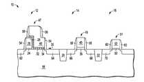
- FIG. 1Shown in FIG. 1 is a semiconductor structure 10 of an integrated circuit having an NVM portion 12 , a high voltage portion 14 , and a logic portion 16 .
- Semiconductor structure 10has a substrate 18 , an isolation region 20 in substrate 18 separating NVM portion 12 from high voltage portion 14 , an isolation region 22 in substrate 18 separating high voltage portion 14 from logic portion 16 , a dielectric layer 24 on substrate 18 in NVM portion 12 and logic portion 16 functioning as a gate dielectric in NVM portion 12 , a conductive layer 26 on dielectric layer 24 in NVM portion and logic portion 16 and functioning as a select gate in NVM portion 12 , and a dielectric layer 28 on conductive layer 26 in NVM portion 12 and logic portion 16 .
- Dielectric layer 24may be a thermal oxide that is grown rather than deposited for high quality.
- Dielectric layer 28may be nitride and be used as an anti-reflective coating.
- Conductive layer 26may be polysilicon that is doped to be conductive.
- NVM portion 12 , high voltage portion 14 , logic portion 16may each be referenced as a region.
- Charge storage layer 30is oxidizable.
- charge storage layer 30includes a nanocrystals surrounded by oxide except where the nanocrystals are over dielectric layer 28 in which case the nanocrystals are directly on dielectric layer 28 for the case where dielectric layer 28 is nitride.
- charge storage layer 30is formed by growing oxide, forming nanocrystals on the grown oxide, and then filling in the regions around and over the nanocrystals with deposited oxide.
- the nanocrystalsmay be silicon.
- An example of the nanocrystalsis shown as nanocrystal 32 .
- dielectric 34The dielectric, which in this example is oxide, surrounding the nanocrystals is shown as dielectric 34 .
- silicon nanocrystals surruounded by oxideis believed to be preferred, some benefit may be obtained by using continuous oxidizable material such as continuous polysilicon surrounded by dielectric that may not include oxide or is some variation on oxide such as oxynitride.
- FIG. 3Shown in FIG. 3 is semiconductor structure 10 after masking NVM portion 12 with a photoresist portion 36 while exposing high voltage portion 14 and logic portion 16 , and then implanting oxygen with implant 38 .
- the energy of the implantis selected to be the depth of the nanocrystals of charge storage layer 30 .
- the dose of the implantis preferably sufficient to fully oxidize the nanocrystals.
- a nitride layercan be deposited on charge storage layer 30 prior to forming photoresist 36 . Then, instead of implanting oxygen, photoresist 36 can be removed and ambient oxygen can be applied that oxidizes the nanocrystals. This leaves charge storage layer 30 in NVM portion 12 with an overlying nitride layer that will be retained so that the resulting NVM cell will have the nitride layer. Sometimes it can be beneficial to have an overlying nitride layer for the charge storage layer. This also avoids requiring an oxygen implant.
- semiconductor structure 10after performing an anneal sufficient to cause a reaction with the silicon nanocrystals and the implanted oxygen. This is performed at a temperature comparable to that used for growing thermal oxide. This temperature may be about 900 degrees Celsius or even more. The temperature may be sufficient to obtain a resulting oxide that is comparable quality to that of thermal oxide. The result is dielectric layer 39 that is on substrate 18 in high voltage portion 14 and over dielectric layer 28 in logic portion 16 .
- semiconductor structure 10after depositing a conductive layer 40 on charge storage layer 30 in NVM portion 12 and on dielectric layer 39 in high voltage portion 14 and in logic portion 16 .
- FIG. 5can be obtained, alternatively, by depositing a conductive layer before implanting the oxygen. This alternative way of obtaining the structure of FIG. 5 is shown in FIGS. 6 and 7 .
- FIG. 6Shown in FIG. 6 is semiconductor structure 10 of FIG. 3 after forming a conductive layer 41 on charge storage layer 30 in NVM portion 12 , high voltage portion 14 , and logic portion 16 , forming a photoresist mask 42 over NVM portion 12 , and performing an implant 44 of oxygen.
- FIG. 7Shown in FIG. 7 is semiconductor structure 10 of FIG. 6 after removing photoresist mask 42 and performing an anneal which causes the nanocrystals that were implanted with oxygen to oxidize and form dielectric layer 46 .
- the annealis preferably at high temperature, which may be 900 degrees Celsius or more, resulting in dielectric layer having comparable quality to that of thermal oxide.
- semiconductor structure 10 of FIG. 7is very similar to semiconductor structure 10 of FIG. 5 . Some differences may occur due to, for example, a portion of oxygen implant being in the lower portion of conductive layer 41 which may cause dielectric layer 46 to be thickened compared to dielectric layer 39 . This may be advantageous if a thicker dielectric is desired. This amount of thickening may be adjusted by varying the depth of the oxygen implant.
- semiconductor structure 10 of FIG. 5after patterning conductive layer 40 to form a high voltage gate in high voltage portion 14 and a control gate in NVM portion 12 .
- the portion of conductive layer 40 in NVM portion 12is the control gate and the portion of conductive layer 40 in high voltage portion 14 is the high voltage gate.
- charge storage layer 30 in NVM portion 12 and dielectric layer 39 in high voltage portion 14is also patterned, in self-aligned fashion, is charge storage layer 30 in NVM portion 12 and dielectric layer 39 in high voltage portion 14 . Dielectric layer 39 is removed from logic portion 16 .
- Metal gate 52may be a stack of conductive layers of which one is metal that sets the work function of the logic transistor to be completed.
- One of the layers in such a stackmay be polysilicon.
- semiconductor structure 10after forming sidewall spacers and source/drain regions to form an NVM cell 47 in NVM portion 12 , a high voltage transistor 49 in high voltage portion 14 , and a logic transistor 51 in logic portion 16 .
- semiconductor 10is shown after forming sidewall spacer 54 around the select gate and a lower portion of the control gate, a sidewall spacer 56 around an upper portion of the control gate, a sidewall spacer 58 around the high voltage gate, a sidewall spacer 60 around gate 52 , source/drain 62 in substrate 18 on the select gate side of NVM cell 47 , a source/drain region 64 in substrate 18 on the select gate side, a source/drain region 66 in substrate 18 on one side of high voltage transistor 49 , a source/drain region 68 in substrate 18 on an opposing side of high voltage transistor 49 , a source/drain region 70 in substrate 18 on one side of logic transistor 51 , and source/drain region 72 in substrate 18 on an opposing side of logic
- the source/drainsmay be silicided as well as the top polysilicon surfaces.
- high voltage transistor 49has a gate of the same material as the control gate of NVM cell 47 , which in this example is polysilicon. This has the benefit of not exposing the top surface of the gate dielectric, dielectric 39 , to an etchant even if implant 38 of FIG. 3 is used.
- Implant 38uses patterned photoresist but the patterning, which removes the undesired portion of the photoresist is not nearly as harsh as a dielectric etch.
- conductive layer 41has the patterned photoresist on it so even the photoresist removal does not contact the top surface of charge storage layer 30 which is converted to dielectric.
- FIG. 11Shown in FIG. 11 is semiconductor structure 10 of FIG. 7 after a different patterning of conductive layer 40 from that shown in FIG. 8 .
- conductive layer 40 in NVM portion 12is patterned the same as in FIG. 8 but, in addition to conductive layer 40 being removed from logic portion 16 , conductive layer 40 is removed from high voltage portion 14 .
- semiconductor structure 10Shown in FIG. 12 is semiconductor structure 10 after removing charge storage layer 30 not covered by the select gate or control gate from NVM portion 12 , and dielectric layer 39 from logic portion 16 . Also removed is dielectric layer 24 , conductive layer 26 , and dielectric layer 28 from logic portion 16 .
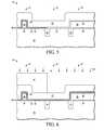
- FIG. 13Shown in FIG. 13 is semiconductor structure 10 after forming a high voltage gate 74 that is a metal gate, which may be a stack, on dielectric layer 39 in high voltage portion 14 , patterning dielectric layer self-aligned to high voltage gate 74 in high voltage portion 14 , a high k gate dielectric 50 in logic portion 16 , and a metal gate 52 that may be a stack in logic portion 16 . Also shown is sidewall spacer and source/drain formation which results in NVM cell 76 in NVM portion 12 , high voltage transistor 78 in high voltage portion 14 , and logic transistor 80 in logic portion 16 .
- a high voltage gate 74that is a metal gate, which may be a stack, on dielectric layer 39 in high voltage portion 14 , patterning dielectric layer self-aligned to high voltage gate 74 in high voltage portion 14 , a high k gate dielectric 50 in logic portion 16 , and a metal gate 52 that may be a stack in logic portion 16 .
- a sidewall spacer 54is formed around the select gate and a lower portion of the control gate, a sidewall spacer 56 is formed around an upper portion of the control gate, a sidewall spacer 58 is formed around high voltage gate 74 , a sidewall spacer 60 is formed around logic gate 52 , a source/drain 62 is formed in substrate 18 on the select gate side, a source/drain 64 is formed in substrate 18 on the control gate side, a source/drain 66 is formed on one side of high voltage transistor, a source/drain 68 is formed on an opposing side of high voltage transistor 78 , a source/drain region 70 is formed on one side of logic transistor 80 , and a source/drain region 72 is formed on an opposing side of logic transistor 80 .
- FIG. 14Shown in FIG. 14 is semiconductor structure 10 of FIG. 13 with more detail concerning the effects of the different etches that occur in the achieving the resulting structure.
- the undesirable effectsinclude a notch 82 at an interface of isolation 20 and NVM portion 12 , a notch 84 at an interface of isolation portion 20 and high voltage portion 14 , a notch 86 at an interface of isolation region 22 and high voltage portion 14 , and a notch 88 at an interface of isolation region 22 and logic portion 16 .
- These notchesarise mostly from oxide growth and subsequent etches.
- the notchis bigger when the grown oxide is thicker such as when the gate dielectric for a high voltage transistor is grown.
- the subsequent etch for removalwhich is always occurs at least for patterning, results in lowering the top surface of the semiconductor substrate and notch creation.
- Semiconductor structure 10shows comparatively less such lowering in logic portion 16 particularly and also in high voltage portion 14 .
- High voltage gate dielectric 39is not completely grown.
- the first portion of charge storage layer 30is grown but the remainder is not.
- the upper oxide layeris deposited and the nanocrystals are oxidized using the implanted oxygen.
- most of the oxide that forms the high voltage gate dielectricis formed from the nanocrystals and deposition instead of consuming substrate 18 .
- With thermal oxide as the basethe subsequent oxides that comprise the majority of the high voltage gate dielectric are brought to a high quality with the high temperature anneal.
- Memory cell 76is configured to operate at voltages between 0 and 18 Volts
- logic transistor 80is configured to operate at voltage between 0 and 3 Volts.
- FIG. 15Shown in FIG. 15 is portion of semiconductor structure 10 of FIG. 14 in more detail showing isolation region 22 , notch 86 at the interface of isolation region 22 and high voltage portion 14 , notch 88 at the interface of isolation region 22 and logic portion 16 , a top surface of substrate 18 in high voltage portion 14 near isolation region 22 , a top surface substrate 18 in logic portion 16 near isolation region 22 , a line 94 that shows where the top surface of substrate 18 would be if high voltage gate dielectric 39 had been grown in both high voltage portion 14 and logic portion 16 , a distance 96 that shows the difference between the actual location of the top surface of substrate 18 and the location where it would be using common thermal oxide growth in high voltage portion 14 , and a distance 98 that shows the difference between the actual location of the top surface of substrate 18 and the location where it would be using common thermal oxide growth in high voltage portion 14 .
- Distance 98is greater than distance 96 .
- Top surface 92is higher than top surface 90 . This is not a normal result. The normal result would
- a method of making a semiconductor structureincluding forming a select gate stack on a substrate, the substrate including a non-volatile memory (NVM) region and a high voltage region, the select gate stack being formed in the NVM region.
- the methodfurther includes forming a charge storage layer over the NVM region and the high voltage region of the substrate, the charge storage layer including charge storage material between a bottom layer of dielectric material and a top layer of dielectric material.
- the methodfurther includes oxidizing the charge storage material in the high voltage region while the charge storage material in the NVM region remains unoxidized.
- the methodmay further include depositing a protective layer over the NVM region before oxidizing the charge storage material.
- the methodmay further include depositing a layer of conductive gate material over the NVM region and the high voltage region and depositing a protective layer over the conductive gate material in the NVM region before oxidizing the charge storage material through the conductive gate material in the high voltage region.
- the methodmay have a further characterization by which the charge storage material includes one of a group consisting of: discrete charge storage elements and a layer of conductive film.
- the methodmay have a further characterization by which the substrate further includes a logic region and the method further includes depositing a material used for a portion of the select gate stack in the NVM region and the logic region, forming a memory cell including the select gate stack in the NVM region, forming a high voltage transistor in the high voltage region, and forming a logic transistor in the logic region after forming the memory cell and the high voltage transistor and after removing the material used for the select gate stack in the logic region.
- the methodmay have a further characterization by which the charge storage layer with the oxidized charge storage material is used as a gate dielectric for a high voltage transistor in the high voltage region.
- the methodmay have a further characterization by which the oxidizing the charge storage material includes implanting oxygen in the charge storage layer in the high voltage region and exposing the charge storage layer to heat.
- the methodmay have a further characterization by which the memory cell is a split gate memory cell.
- the methodmay have a further characterization by which the memory cell is configured to operate at voltages between 0 and 18 Volts and the logic transistor is configured to operate at voltage between 0 and 3 Volts.
- the methodmay further include forming a control gate for a memory cell from the layer of conductive gate material in the NVM region and forming a control gate for a high voltage device cell from the layer of conductive gate material in the high voltage region.
- Also described is a method of making a semiconductor structureincluding forming growing a select gate dielectric over a major surface of a substrate.
- the methodfurther includes depositing a select gate material over the select gate dielectric.
- the methodfurther includes patterning a select gate stack in a non-volatile memory (NVM) region of the substrate while removing the select gate dielectric and the select gate material in a high voltage region of the substrate and retaining the select gate dielectric and the select gate material in a logic region of the substrate.
- the methodfurther includes depositing a charge storage layer over the NVM region, the high voltage region, and the logic region.
- the methodfurther includes forming a protective layer over the charge storage layer in the NVM region.
- the methodfurther includes oxidizing the charge storage layer in the high voltage region and the logic region while the protective layer prevents the charge storage layer from oxidizing in the NVM region.
- the methodmay further include depositing a control gate material over the charge storage layer before the forming the protective layer and the oxidizing the charge storage layer.
- the methodmay further include patterning the control gate material and the charge storage layer in the NVM region to form a control gate partially overlapping the select gate stack.
- the methodmay further include patterning the control gate material and the oxidized charge storage layer in the high voltage region to form a gate for a high voltage device.
- the methodmay further include removing the select gate dielectric and the select gate material in the logic region of the substrate and forming a gate stack in the logic region after the removing the select gate dielectric and the select gate material in the logic region.
- a semiconductor structurethat includes a substrate including a non-volatile memory (NVM) region, a high voltage region and a logic region.
- the semiconductor structurefurther includes an NVM cell configured in the NVM region.
- the semiconductor structurefurther includes a high voltage device configured in the high voltage region.
- the semiconductor structurefurther includes a logic device configured in the logic region.
- the semiconductor structurefurther includes a first trench isolation region between the NVM region and the high voltage region.
- the semiconductor structurefurther includes a second trench isolation region between the high voltage region and the logic region.
- the semiconductor structurefurther includes a height of a major surface of the substrate abutting the second trench isolation region in the high voltage region is less than a height of the major surface of the substrate abutting the second trench isolation region in the logic region.
- the semiconductor structuremay further include a select gate, a control gate overlapping a portion of the select gate, and a charge storage layer between the select gate and the control gate.
- the semiconductor structuremay have a further characterization by which the high voltage device further includes a gate dielectric formed of an oxidized portion of the charge storage layer.
- the semiconductor structuremay have a further characterization by which the NVM cell is configured to operate at voltages between 0 and 18 Volts, the high voltage device is configured to operate at voltages between 0 and 18 Volts, and the logic device is configured to operate at voltage between 0 and 3 Volts.
- the semiconductor structuremay have a further characterization by which the charge storage layer includes one of a group consisting of: discrete charge storage elements between top and bottom dielectric layers, and a layer of conductive film between top and bottom dielectric layers.
Landscapes
- Engineering & Computer Science (AREA)
- Manufacturing & Machinery (AREA)
- Non-Volatile Memory (AREA)
- Semiconductor Memories (AREA)
Abstract
Description
- 1. Field
- This disclosure relates generally to non-volatile memories (NVMs), and more particularly, integrating NVMs with high voltage transistors.
- 2. Related Art
- The integration of non-volatile memories (NVMs) with high voltage transistors is particularly significant because NVM cells typically use significantly higher voltages for program and erase than the power supply voltage. Most of the transistors generally operate at the power supply voltage and are manufactured with that voltage in mind. The generation and use of the higher voltages required for program and erase require transistors that can operate at those higher voltages. Also, it is common for there to be a need for some ability to handle higher voltages than are used by most of the logic transistors, especially at inputs which can be from higher voltage products such as batteries and even USB inputs. This is often a situation of an analog to digital conversion. The high voltage transistors typically have a thicker gate dielectric than the vast majority of the logic transistors which can create difficulties in manufacturing. The desire is to have a high quality gate dielectric regardless of the thickness. Thermally grown oxides for this purpose are typically the highest quality gate dielectric but it is also desirable to avoid removing a layer on the gate dielectric by etching. Achieving both of these desirable characteristics can be difficult to achieve. Also there is an undesirable effect of having to grow a particularly thick oxide which consumes silicon and thus lowers the top surface of the semiconductor substrate. In etching this and other oxides, there are divots formed at the interface between the isolation regions and the active regions.
- Accordingly there is a need to provide a high voltage transistor integration that improves upon one or more of the issues raised above.
- The present invention is illustrated by way of example and is not limited by the accompanying figures, in which like references indicate similar elements. Elements in the figures are illustrated for simplicity and clarity and have not necessarily been drawn to scale.
FIG. 1 is a cross section of a semiconductor structure having a non-volatile memory (NVM) structure, a high voltage transistor structure, and a logic transistor structure at a stage in processing according to an embodiment;FIG. 2 is a cross section of the semiconductor structure ofFIG. 1 at a subsequent stage in processing;FIG. 3 is a cross section of the semiconductor structure ofFIG. 2 at a subsequent stage in processing;FIG. 4 is a cross section of the semiconductor structure ofFIG. 3 at a subsequent stage in processing;FIG. 5 is a cross section of the semiconductor structure ofFIG. 4 at a subsequent stage in processing;FIG. 6 is a cross section of the semiconductor structure ofFIG. 2 at a subsequent stage in processing as an alternative to that shown inFIG. 3 according to a second embodiment;FIG. 7 is a cross section of the semiconductor structure ofFIG. 6 at a subsequent stage in processing that substantially achieves the structure ofFIG. 5 ;FIG. 8 is a cross section of the semiconductor structure ofFIG. 5 at a subsequent stage in processing;FIG. 9 is a cross section of the semiconductor structure ofFIG. 8 at a subsequent stage in processing;FIG. 10 is a cross section of the semiconductor structure ofFIG. 9 at a subsequent stage in processing;FIG. 11 is a cross section of the semiconductor structure ofFIG. 5 at a subsequent stage in processing according to an alternative to the semiconductor structure ofFIG. 8 ;FIG. 12 is a cross section of the semiconductor structure ofFIG. 11 at a subsequent stage in processing;FIG. 13 is a cross section of the semiconductor structure ofFIG. 12 at a subsequent stage in processingFIG. 14 is a cross section of the semiconductor structure ofFIG. 13 in more detail; andFIG. 15 is cross section of portion of the semiconductor structure ofFIG. 14 in more detail.- In one aspect, an integration of a non-volatile memory (NVM) cell and a high voltage transistor includes forming the select gate structure of the NVM cell in the NVM portion and an oxidizable charge storage layer wherein the oxidizable charge storage layer extends to the region of forming the high voltage transistor. The oxidizable charge storage layer is protected for the NVM cell while being oxidized for the high voltage transistor to form a thick oxide layer. The subsequent completion of the high voltage transistor uses the thick oxide for the gate dielectric of the high voltage transistor. This is better understood by reference to the drawings the following the written description.
- The semiconductor substrate described herein can be any semiconductor material or combinations of materials, such as gallium arsenide, silicon germanium, silicon-on-insulator (SOI), silicon, monocrystalline silicon, the like, and combinations of the above. Oxide layer refers to a silicon oxide layer unless otherwise noted. Similarly, nitride layer refers to a silicon nitride layer unless otherwise noted.
- Shown in
FIG. 1 is asemiconductor structure 10 of an integrated circuit having anNVM portion 12, ahigh voltage portion 14, and alogic portion 16.Semiconductor structure 10 has asubstrate 18, anisolation region 20 insubstrate 18 separatingNVM portion 12 fromhigh voltage portion 14, anisolation region 22 insubstrate 18 separatinghigh voltage portion 14 fromlogic portion 16, adielectric layer 24 onsubstrate 18 inNVM portion 12 andlogic portion 16 functioning as a gate dielectric inNVM portion 12, aconductive layer 26 ondielectric layer 24 in NVM portion andlogic portion 16 and functioning as a select gate inNVM portion 12, and adielectric layer 28 onconductive layer 26 inNVM portion 12 andlogic portion 16.Dielectric layer 24 may be a thermal oxide that is grown rather than deposited for high quality.Dielectric layer 28 may be nitride and be used as an anti-reflective coating.Conductive layer 26 may be polysilicon that is doped to be conductive.NVM portion 12,high voltage portion 14,logic portion 16 may each be referenced as a region. - Shown in
FIG. 2 issemiconductor structure 10 after forming acharge storage layer 30 inNVM portion 12,high voltage portion 14, andlogic portion 16.Charge storage layer 30 is oxidizable. In this example,charge storage layer 30 includes a nanocrystals surrounded by oxide except where the nanocrystals are overdielectric layer 28 in which case the nanocrystals are directly ondielectric layer 28 for the case wheredielectric layer 28 is nitride. In the example shown,charge storage layer 30 is formed by growing oxide, forming nanocrystals on the grown oxide, and then filling in the regions around and over the nanocrystals with deposited oxide. The nanocrystals may be silicon. An example of the nanocrystals is shown asnanocrystal 32. The dielectric, which in this example is oxide, surrounding the nanocrystals is shown as dielectric34. Although silicon nanocrystals surruounded by oxide is believed to be preferred, some benefit may be obtained by using continuous oxidizable material such as continuous polysilicon surrounded by dielectric that may not include oxide or is some variation on oxide such as oxynitride. - Shown in
FIG. 3 issemiconductor structure 10 after maskingNVM portion 12 with aphotoresist portion 36 while exposinghigh voltage portion 14 andlogic portion 16, and then implanting oxygen with implant38. The energy of the implant is selected to be the depth of the nanocrystals ofcharge storage layer 30. The dose of the implant is preferably sufficient to fully oxidize the nanocrystals. - For the case of
charge storage layer 30 having a top oxide, a nitride layer can be deposited oncharge storage layer 30 prior to formingphotoresist 36. Then, instead of implanting oxygen,photoresist 36 can be removed and ambient oxygen can be applied that oxidizes the nanocrystals. This leavescharge storage layer 30 inNVM portion 12 with an overlying nitride layer that will be retained so that the resulting NVM cell will have the nitride layer. Sometimes it can be beneficial to have an overlying nitride layer for the charge storage layer. This also avoids requiring an oxygen implant. - Shown in
FIG. 4 issemiconductor structure 10 after performing an anneal sufficient to cause a reaction with the silicon nanocrystals and the implanted oxygen. This is performed at a temperature comparable to that used for growing thermal oxide. This temperature may be about 900 degrees Celsius or even more. The temperature may be sufficient to obtain a resulting oxide that is comparable quality to that of thermal oxide. The result isdielectric layer 39 that is onsubstrate 18 inhigh voltage portion 14 and overdielectric layer 28 inlogic portion 16. - Shown in
FIG. 5 issemiconductor structure 10 after depositing aconductive layer 40 oncharge storage layer 30 inNVM portion 12 and ondielectric layer 39 inhigh voltage portion 14 and inlogic portion 16. - The structure shown in
FIG. 5 can be obtained, alternatively, by depositing a conductive layer before implanting the oxygen. This alternative way of obtaining the structure ofFIG. 5 is shown inFIGS. 6 and 7 . - Shown in
FIG. 6 issemiconductor structure 10 ofFIG. 3 after forming aconductive layer 41 oncharge storage layer 30 inNVM portion 12,high voltage portion 14, andlogic portion 16, forming aphotoresist mask 42 overNVM portion 12, and performing animplant 44 of oxygen. - Shown in
FIG. 7 issemiconductor structure 10 ofFIG. 6 after removingphotoresist mask 42 and performing an anneal which causes the nanocrystals that were implanted with oxygen to oxidize and formdielectric layer 46. As for the oxidation described forFIG. 4 , the anneal is preferably at high temperature, which may be 900 degrees Celsius or more, resulting in dielectric layer having comparable quality to that of thermal oxide. As can be seen,semiconductor structure 10 ofFIG. 7 is very similar tosemiconductor structure 10 ofFIG. 5 . Some differences may occur due to, for example, a portion of oxygen implant being in the lower portion ofconductive layer 41 which may causedielectric layer 46 to be thickened compared todielectric layer 39. This may be advantageous if a thicker dielectric is desired. This amount of thickening may be adjusted by varying the depth of the oxygen implant. - Continuing the flow from
semiconductor structure 10 ofFIG. 5 , shown inFIG. 8 issemiconductor structure 10 ofFIG. 5 after patterningconductive layer 40 to form a high voltage gate inhigh voltage portion 14 and a control gate inNVM portion 12. The portion ofconductive layer 40 inNVM portion 12 is the control gate and the portion ofconductive layer 40 inhigh voltage portion 14 is the high voltage gate. Also patterned, in self-aligned fashion, ischarge storage layer 30 inNVM portion 12 anddielectric layer 39 inhigh voltage portion 14.Dielectric layer 39 is removed fromlogic portion 16. - Shown in
FIG. 9 issemiconductor structure 10 after removingdielectric layer 28,conductive layer 26, and gate dielectric24 fromlogic portion 16 and forming agate stack 48 having ahigh k dielectric 50 and ametal gate 52 inlogic portion 16.Metal gate 52 may be a stack of conductive layers of which one is metal that sets the work function of the logic transistor to be completed. One of the layers in such a stack may be polysilicon. - Shown in
FIG. 10 issemiconductor structure 10 after forming sidewall spacers and source/drain regions to form anNVM cell 47 inNVM portion 12, ahigh voltage transistor 49 inhigh voltage portion 14, and alogic transistor 51 inlogic portion 16. In particular,semiconductor 10 is shown after formingsidewall spacer 54 around the select gate and a lower portion of the control gate, asidewall spacer 56 around an upper portion of the control gate, asidewall spacer 58 around the high voltage gate, asidewall spacer 60 aroundgate 52, source/drain 62 insubstrate 18 on the select gate side ofNVM cell 47, a source/drain region 64 insubstrate 18 on the select gate side, a source/drain region 66 insubstrate 18 on one side ofhigh voltage transistor 49, a source/drain region 68 insubstrate 18 on an opposing side ofhigh voltage transistor 49, a source/drain region 70 insubstrate 18 on one side oflogic transistor 51, and source/drain region72 insubstrate 18 on an opposing side oflogic transistor 51. The source/drains may be silicided as well as the top polysilicon surfaces. In this casehigh voltage transistor 49 has a gate of the same material as the control gate ofNVM cell 47, which in this example is polysilicon. This has the benefit of not exposing the top surface of the gate dielectric, dielectric39, to an etchant even if implant38 ofFIG. 3 is used. Implant38 uses patterned photoresist but the patterning, which removes the undesired portion of the photoresist is not nearly as harsh as a dielectric etch. In the process in which implant44 is used,conductive layer 41 has the patterned photoresist on it so even the photoresist removal does not contact the top surface ofcharge storage layer 30 which is converted to dielectric. - Shown in
FIG. 11 issemiconductor structure 10 ofFIG. 7 after a different patterning ofconductive layer 40 from that shown inFIG. 8 . InFIG. 11 conductive layer 40 inNVM portion 12 is patterned the same as inFIG. 8 but, in addition toconductive layer 40 being removed fromlogic portion 16,conductive layer 40 is removed fromhigh voltage portion 14. - Shown in
FIG. 12 issemiconductor structure 10 after removingcharge storage layer 30 not covered by the select gate or control gate fromNVM portion 12, anddielectric layer 39 fromlogic portion 16. Also removed isdielectric layer 24,conductive layer 26, anddielectric layer 28 fromlogic portion 16. - Shown in
FIG. 13 issemiconductor structure 10 after forming ahigh voltage gate 74 that is a metal gate, which may be a stack, ondielectric layer 39 inhigh voltage portion 14, patterning dielectric layer self-aligned tohigh voltage gate 74 inhigh voltage portion 14, a highk gate dielectric 50 inlogic portion 16, and ametal gate 52 that may be a stack inlogic portion 16. Also shown is sidewall spacer and source/drain formation which results inNVM cell 76 inNVM portion 12,high voltage transistor 78 inhigh voltage portion 14, andlogic transistor 80 inlogic portion 16. Asidewall spacer 54 is formed around the select gate and a lower portion of the control gate, asidewall spacer 56 is formed around an upper portion of the control gate, asidewall spacer 58 is formed aroundhigh voltage gate 74, asidewall spacer 60 is formed aroundlogic gate 52, a source/drain 62 is formed insubstrate 18 on the select gate side, a source/drain 64 is formed insubstrate 18 on the control gate side, a source/drain 66 is formed on one side of high voltage transistor, a source/drain 68 is formed on an opposing side ofhigh voltage transistor 78, a source/drain region 70 is formed on one side oflogic transistor 80, and a source/drain region72 is formed on an opposing side oflogic transistor 80. This shows the formation of a metal gate forhigh voltage transistor 78. This most likely involves removing polysilicon from dielectric39 with an etch, which is generally not preferable, but the benefits of using metal gate may make this desirable in some situations. - Shown in
FIG. 14 issemiconductor structure 10 ofFIG. 13 with more detail concerning the effects of the different etches that occur in the achieving the resulting structure. The undesirable effects include anotch 82 at an interface ofisolation 20 andNVM portion 12, anotch 84 at an interface ofisolation portion 20 andhigh voltage portion 14, anotch 86 at an interface ofisolation region 22 andhigh voltage portion 14, and anotch 88 at an interface ofisolation region 22 andlogic portion 16. These notches arise mostly from oxide growth and subsequent etches. The notch is bigger when the grown oxide is thicker such as when the gate dielectric for a high voltage transistor is grown. The subsequent etch for removal, which is always occurs at least for patterning, results in lowering the top surface of the semiconductor substrate and notch creation.Semiconductor structure 10 shows comparatively less such lowering inlogic portion 16 particularly and also inhigh voltage portion 14. Highvoltage gate dielectric 39 is not completely grown. The first portion ofcharge storage layer 30 is grown but the remainder is not. The upper oxide layer is deposited and the nanocrystals are oxidized using the implanted oxygen. Thus most of the oxide that forms the high voltage gate dielectric is formed from the nanocrystals and deposition instead of consumingsubstrate 18. With thermal oxide as the base, the subsequent oxides that comprise the majority of the high voltage gate dielectric are brought to a high quality with the high temperature anneal.Memory cell 76 is configured to operate at voltages between 0 and 18 Volts, andlogic transistor 80 is configured to operate at voltage between 0 and 3 Volts. - Shown in
FIG. 15 is portion ofsemiconductor structure 10 ofFIG. 14 in more detail showingisolation region 22, notch86 at the interface ofisolation region 22 andhigh voltage portion 14, notch88 at the interface ofisolation region 22 andlogic portion 16, a top surface ofsubstrate 18 inhigh voltage portion 14 nearisolation region 22, atop surface substrate 18 inlogic portion 16 nearisolation region 22, aline 94 that shows where the top surface ofsubstrate 18 would be if highvoltage gate dielectric 39 had been grown in bothhigh voltage portion 14 andlogic portion 16, adistance 96 that shows the difference between the actual location of the top surface ofsubstrate 18 and the location where it would be using common thermal oxide growth inhigh voltage portion 14, and adistance 98 that shows the difference between the actual location of the top surface ofsubstrate 18 and the location where it would be using common thermal oxide growth inhigh voltage portion 14.Distance 98 is greater thandistance 96.Top surface 92 is higher thantop surface 90. This is not a normal result. The normal result would be for the top surfaces of the active regions to be nearly equal. - By now it should be appreciated that there has been provided a method of making a semiconductor structure including forming a select gate stack on a substrate, the substrate including a non-volatile memory (NVM) region and a high voltage region, the select gate stack being formed in the NVM region. The method further includes forming a charge storage layer over the NVM region and the high voltage region of the substrate, the charge storage layer including charge storage material between a bottom layer of dielectric material and a top layer of dielectric material. The method further includes oxidizing the charge storage material in the high voltage region while the charge storage material in the NVM region remains unoxidized. The method may further include depositing a protective layer over the NVM region before oxidizing the charge storage material. The method may further include depositing a layer of conductive gate material over the NVM region and the high voltage region and depositing a protective layer over the conductive gate material in the NVM region before oxidizing the charge storage material through the conductive gate material in the high voltage region. The method may have a further characterization by which the charge storage material includes one of a group consisting of: discrete charge storage elements and a layer of conductive film. The method may have a further characterization by which the substrate further includes a logic region and the method further includes depositing a material used for a portion of the select gate stack in the NVM region and the logic region, forming a memory cell including the select gate stack in the NVM region, forming a high voltage transistor in the high voltage region, and forming a logic transistor in the logic region after forming the memory cell and the high voltage transistor and after removing the material used for the select gate stack in the logic region. The method may have a further characterization by which the charge storage layer with the oxidized charge storage material is used as a gate dielectric for a high voltage transistor in the high voltage region. The method may have a further characterization by which the oxidizing the charge storage material includes implanting oxygen in the charge storage layer in the high voltage region and exposing the charge storage layer to heat. The method may have a further characterization by which the memory cell is a split gate memory cell. The method may have a further characterization by which the memory cell is configured to operate at voltages between 0 and 18 Volts and the logic transistor is configured to operate at voltage between 0 and 3 Volts. The method may further include forming a control gate for a memory cell from the layer of conductive gate material in the NVM region and forming a control gate for a high voltage device cell from the layer of conductive gate material in the high voltage region.
- Also described is a method of making a semiconductor structure including forming growing a select gate dielectric over a major surface of a substrate. The method further includes depositing a select gate material over the select gate dielectric. The method further includes patterning a select gate stack in a non-volatile memory (NVM) region of the substrate while removing the select gate dielectric and the select gate material in a high voltage region of the substrate and retaining the select gate dielectric and the select gate material in a logic region of the substrate. The method further includes depositing a charge storage layer over the NVM region, the high voltage region, and the logic region. The method further includes forming a protective layer over the charge storage layer in the NVM region. The method further includes oxidizing the charge storage layer in the high voltage region and the logic region while the protective layer prevents the charge storage layer from oxidizing in the NVM region. The method may further include depositing a control gate material over the charge storage layer before the forming the protective layer and the oxidizing the charge storage layer. The method may further include patterning the control gate material and the charge storage layer in the NVM region to form a control gate partially overlapping the select gate stack. The method may further include patterning the control gate material and the oxidized charge storage layer in the high voltage region to form a gate for a high voltage device. The method may further include removing the select gate dielectric and the select gate material in the logic region of the substrate and forming a gate stack in the logic region after the removing the select gate dielectric and the select gate material in the logic region.
- Described also is a semiconductor structure that includes a substrate including a non-volatile memory (NVM) region, a high voltage region and a logic region. The semiconductor structure further includes an NVM cell configured in the NVM region. The semiconductor structure further includes a high voltage device configured in the high voltage region. The semiconductor structure further includes a logic device configured in the logic region. The semiconductor structure further includes a first trench isolation region between the NVM region and the high voltage region. The semiconductor structure further includes a second trench isolation region between the high voltage region and the logic region. The semiconductor structure further includes a height of a major surface of the substrate abutting the second trench isolation region in the high voltage region is less than a height of the major surface of the substrate abutting the second trench isolation region in the logic region. The semiconductor structure may further include a select gate, a control gate overlapping a portion of the select gate, and a charge storage layer between the select gate and the control gate. The semiconductor structure may have a further characterization by which the high voltage device further includes a gate dielectric formed of an oxidized portion of the charge storage layer. The semiconductor structure may have a further characterization by which the NVM cell is configured to operate at voltages between 0 and 18 Volts, the high voltage device is configured to operate at voltages between 0 and 18 Volts, and the logic device is configured to operate at voltage between 0 and 3 Volts. The semiconductor structure may have a further characterization by which the charge storage layer includes one of a group consisting of: discrete charge storage elements between top and bottom dielectric layers, and a layer of conductive film between top and bottom dielectric layers.
- Moreover, the terms “front,” “back,” “top,” “bottom,” “over,” “under” and the like in the description and in the claims, if any, are used for descriptive purposes and not necessarily for describing permanent relative positions. It is understood that the terms so used are interchangeable under appropriate circumstances such that the embodiments of the invention described herein are, for example, capable of operation in other orientations than those illustrated or otherwise described herein.
- Although the invention is described herein with reference to specific embodiments, various modifications and changes can be made without departing from the scope of the present invention as set forth in the claims below. For example there may be additional transistor types and there may be additional gate dielectric thicknesses from those shown. Accordingly, the specification and figures are to be regarded in an illustrative rather than a restrictive sense, and all such modifications are intended to be included within the scope of the present invention. Any benefits, advantages, or solutions to problems that are described herein with regard to specific embodiments are not intended to be construed as a critical, required, or essential feature or element of any or all the claims.
- Furthermore, the terms “a” or “an,” as used herein, are defined as one or more than one. Also, the use of introductory phrases such as “at least one” and “one or more” in the claims should not be construed to imply that the introduction of another claim element by the indefinite articles “a” or “an” limits any particular claim containing such introduced claim element to inventions containing only one such element, even when the same claim includes the introductory phrases “one or more” or “at least one” and indefinite articles such as “a” or “an.” The same holds true for the use of definite articles.
Claims (20)
Priority Applications (1)
| Application Number | Priority Date | Filing Date | Title |
|---|---|---|---|
| US13/928,666US9006093B2 (en) | 2013-06-27 | 2013-06-27 | Non-volatile memory (NVM) and high voltage transistor integration |
Applications Claiming Priority (1)
| Application Number | Priority Date | Filing Date | Title |
|---|---|---|---|
| US13/928,666US9006093B2 (en) | 2013-06-27 | 2013-06-27 | Non-volatile memory (NVM) and high voltage transistor integration |
Publications (2)
| Publication Number | Publication Date |
|---|---|
| US20150001612A1true US20150001612A1 (en) | 2015-01-01 |
| US9006093B2 US9006093B2 (en) | 2015-04-14 |
Family
ID=52114745
Family Applications (1)
| Application Number | Title | Priority Date | Filing Date |
|---|---|---|---|
| US13/928,666ActiveUS9006093B2 (en) | 2013-06-27 | 2013-06-27 | Non-volatile memory (NVM) and high voltage transistor integration |
Country Status (1)
| Country | Link |
|---|---|
| US (1) | US9006093B2 (en) |
Cited By (2)
| Publication number | Priority date | Publication date | Assignee | Title |
|---|---|---|---|---|
| US10381359B2 (en)* | 2015-07-21 | 2019-08-13 | Silicon Storage Technology, Inc. | Non-volatile split game memory cells with integrated high K metal gate logic device and metal-free erase gate, and method of making same |
| CN113192957A (en)* | 2021-04-27 | 2021-07-30 | 上海华虹宏力半导体制造有限公司 | Method for manufacturing flash memory |
Families Citing this family (1)
| Publication number | Priority date | Publication date | Assignee | Title |
|---|---|---|---|---|
| US9275864B2 (en)* | 2013-08-22 | 2016-03-01 | Freescale Semiconductor,Inc. | Method to form a polysilicon nanocrystal thin film storage bitcell within a high k metal gate platform technology using a gate last process to form transistor gates |
Citations (6)
| Publication number | Priority date | Publication date | Assignee | Title |
|---|---|---|---|---|
| US20090050955A1 (en)* | 2007-08-24 | 2009-02-26 | Kenichi Akita | Nonvolatile semiconductor device and method of manufacturing the same |
| US20120248523A1 (en)* | 2011-03-31 | 2012-10-04 | Shroff Mehul D | Non-volatile memory and logic circuit process integration |
| US20130323922A1 (en)* | 2011-09-29 | 2013-12-05 | Freescale Semiconductor, Inc. | Split gate memory device with gap spacer |
| US20140035027A1 (en)* | 2009-11-25 | 2014-02-06 | Renesas Electronics Corporation | Semiconductor device and a manufacturing method thereof |
| US20140050029A1 (en)* | 2012-08-20 | 2014-02-20 | Sung-taeg Kang | Split-gate memory cells having select-gate sidewall metal silicide regions and related manufacturing methods |
| US20140120713A1 (en)* | 2012-10-26 | 2014-05-01 | Mehul D. Shroff | Method of making a logic transistor and a non-volatile memory (nvm) cell |
Family Cites Families (109)
| Publication number | Priority date | Publication date | Assignee | Title |
|---|---|---|---|---|
| US5445984A (en) | 1994-11-28 | 1995-08-29 | United Microelectronics Corporation | Method of making a split gate flash memory cell |
| US6087225A (en) | 1998-02-05 | 2000-07-11 | International Business Machines Corporation | Method for dual gate oxide dual workfunction CMOS |
| JP3023355B1 (en) | 1998-12-25 | 2000-03-21 | 松下電器産業株式会社 | Semiconductor device and manufacturing method thereof |
| JP4068746B2 (en) | 1998-12-25 | 2008-03-26 | 株式会社ルネサステクノロジ | Semiconductor integrated circuit device |
| AU3073800A (en) | 1999-02-01 | 2000-08-25 | Hitachi Limited | Semiconductor integrated circuit and nonvolatile memory element |
| EP1039533A3 (en) | 1999-03-22 | 2001-04-04 | Infineon Technologies North America Corp. | High performance dram and method of manufacture |
| US6194301B1 (en) | 1999-07-12 | 2001-02-27 | International Business Machines Corporation | Method of fabricating an integrated circuit of logic and memory using damascene gate structure |
| EP1139419A1 (en) | 2000-03-29 | 2001-10-04 | STMicroelectronics S.r.l. | Method of manufacturing an electrically programmable, non-volatile memory with logic circuitry |
| JP4096507B2 (en) | 2000-09-29 | 2008-06-04 | 富士通株式会社 | Manufacturing method of semiconductor device |
| KR100359780B1 (en) | 2000-11-22 | 2002-11-04 | 주식회사 하이닉스반도체 | Method for Fabricating of Semiconductor device |
| US6531350B2 (en) | 2001-02-22 | 2003-03-11 | Halo, Inc. | Twin MONOS cell fabrication method and array organization |
| JP2003023114A (en) | 2001-07-05 | 2003-01-24 | Fujitsu Ltd | Semiconductor integrated circuit device and method of manufacturing the same |
| JP3993438B2 (en) | 2002-01-25 | 2007-10-17 | 株式会社ルネサステクノロジ | Semiconductor device |
| AU2003215062B2 (en) | 2002-02-08 | 2008-06-19 | Genencor International, Inc. | Secretion, transcription and sporulation genes in Bacillus clausii |
| US6531734B1 (en) | 2002-05-24 | 2003-03-11 | Silicon Based Technology Corp. | Self-aligned split-gate flash memory cell having an integrated source-side erase structure and its contactless flash memory arrays |
| US6635526B1 (en) | 2002-06-07 | 2003-10-21 | Infineon Technologies Ag | Structure and method for dual work function logic devices in vertical DRAM process |
| US6777761B2 (en) | 2002-08-06 | 2004-08-17 | International Business Machines Corporation | Semiconductor chip using both polysilicon and metal gate devices |
| US6808983B2 (en) | 2002-08-27 | 2004-10-26 | Micron Technology, Inc. | Silicon nanocrystal capacitor and process for forming same |
| US6909139B2 (en) | 2003-06-27 | 2005-06-21 | Infineon Technologies Ag | One transistor flash memory cell |
| JP2005026380A (en) | 2003-06-30 | 2005-01-27 | Toshiba Corp | Semiconductor device including nonvolatile memory and manufacturing method thereof |
| JP2005072237A (en) | 2003-08-25 | 2005-03-17 | Renesas Technology Corp | Manufacturing method of semiconductor device |
| US7141468B2 (en) | 2003-10-27 | 2006-11-28 | Texas Instruments Incorporated | Application of different isolation schemes for logic and embedded memory |
| US7229880B2 (en) | 2003-11-19 | 2007-06-12 | Promos Technologies Inc. | Precision creation of inter-gates insulator |
| US6939767B2 (en) | 2003-11-19 | 2005-09-06 | Freescale Semiconductor, Inc. | Multi-bit non-volatile integrated circuit memory and method therefor |
| US7154779B2 (en) | 2004-01-21 | 2006-12-26 | Sandisk Corporation | Non-volatile memory cell using high-k material inter-gate programming |
| KR100528486B1 (en) | 2004-04-12 | 2005-11-15 | 삼성전자주식회사 | Non-volatile memory devices and method for forming the same |
| JP2006059880A (en) | 2004-08-17 | 2006-03-02 | Fujitsu Ltd | Semiconductor device and manufacturing method thereof |
| US7026689B2 (en) | 2004-08-27 | 2006-04-11 | Taiwan Semiconductor Manufacturing Company | Metal gate structure for MOS devices |
| KR100688575B1 (en) | 2004-10-08 | 2007-03-02 | 삼성전자주식회사 | Nonvolatile Semiconductor Memory Devices |
| JP4578938B2 (en) | 2004-11-08 | 2010-11-10 | 富士通セミコンダクター株式会社 | Semiconductor device |
| US7361543B2 (en) | 2004-11-12 | 2008-04-22 | Freescale Semiconductor, Inc. | Method of forming a nanocluster charge storage device |
| US7208793B2 (en) | 2004-11-23 | 2007-04-24 | Micron Technology, Inc. | Scalable integrated logic and non-volatile memory |
| KR100654341B1 (en) | 2004-12-08 | 2006-12-08 | 삼성전자주식회사 | Nonvolatile Memory Device and Manufacturing Method Thereof |
| US7365389B1 (en) | 2004-12-10 | 2008-04-29 | Spansion Llc | Memory cell having enhanced high-K dielectric |
| US7482223B2 (en) | 2004-12-22 | 2009-01-27 | Sandisk Corporation | Multi-thickness dielectric for semiconductor memory |
| US7202125B2 (en) | 2004-12-22 | 2007-04-10 | Sandisk Corporation | Low-voltage, multiple thin-gate oxide and low-resistance gate electrode |
| US7183159B2 (en) | 2005-01-14 | 2007-02-27 | Freescale Semiconductor, Inc. | Method of forming an integrated circuit having nanocluster devices and non-nanocluster devices |
| KR100646085B1 (en) | 2005-03-08 | 2006-11-14 | 매그나칩 반도체 유한회사 | Nonvolatile memory device, method for manufacturing same, and method for manufacturing semiconductor device using same |
| US7563662B2 (en) | 2005-03-18 | 2009-07-21 | Freescale Semiconductor, Inc. | Processes for forming electronic devices including non-volatile memory |
| KR101058445B1 (en) | 2005-05-23 | 2011-08-24 | 후지쯔 세미컨덕터 가부시키가이샤 | Semiconductor device |
| US7547599B2 (en) | 2005-05-26 | 2009-06-16 | Micron Technology, Inc. | Multi-state memory cell |
| US7229873B2 (en) | 2005-08-10 | 2007-06-12 | Texas Instruments Incorporated | Process for manufacturing dual work function metal gates in a microelectronics device |
| US7456465B2 (en) | 2005-09-30 | 2008-11-25 | Freescale Semiconductor, Inc. | Split gate memory cell and method therefor |
| JP4928890B2 (en) | 2005-10-14 | 2012-05-09 | 株式会社東芝 | Nonvolatile semiconductor memory device |
| TWI277180B (en) | 2005-12-14 | 2007-03-21 | Fujitsu Ltd | Semiconductor device and the manufacturing method thereof |
| US7544980B2 (en) | 2006-01-27 | 2009-06-09 | Freescale Semiconductor, Inc. | Split gate memory cell in a FinFET |
| JP4575320B2 (en) | 2006-03-15 | 2010-11-04 | 株式会社東芝 | Nonvolatile semiconductor memory device |
| JP2007258224A (en) | 2006-03-20 | 2007-10-04 | Renesas Technology Corp | Semiconductor integrated circuit device and manufacturing method thereof |
| US20070224772A1 (en) | 2006-03-21 | 2007-09-27 | Freescale Semiconductor, Inc. | Method for forming a stressor structure |
| US20070249129A1 (en) | 2006-04-21 | 2007-10-25 | Freescale Semiconductor, Inc. | STI stressor integration for minimal phosphoric exposure and divot-free topography |
| KR20080010900A (en) | 2006-07-28 | 2008-01-31 | 삼성전자주식회사 | Nonvolatile Memory Device, Operation Method and Manufacturing Method Thereof |
| JP5142494B2 (en) | 2006-08-03 | 2013-02-13 | ルネサスエレクトロニクス株式会社 | Manufacturing method of semiconductor device |
| KR100812237B1 (en) | 2006-08-25 | 2008-03-10 | 삼성전자주식회사 | Manufacturing Method of Embedded Flash Memory Device |
| US7524719B2 (en) | 2006-08-31 | 2009-04-28 | Freescale Semiconductor, Inc. | Method of making self-aligned split gate memory cell |
| KR100755410B1 (en) | 2006-09-22 | 2007-09-04 | 삼성전자주식회사 | Gate structure and method for forming same, nonvolatile memory device and method for manufacturing same |
| KR100845720B1 (en) | 2006-11-30 | 2008-07-10 | 동부일렉트로닉스 주식회사 | Flash memory device and manufacturing method thereof |
| CN100590853C (en) | 2006-12-15 | 2010-02-17 | 中芯国际集成电路制造(上海)有限公司 | Semiconductor memory and method of forming the same |
| US8410543B2 (en) | 2007-02-01 | 2013-04-02 | Renesas Electronics Corporation | Semiconductor storage device and manufacturing method thereof |
| JP2008192991A (en) | 2007-02-07 | 2008-08-21 | Toshiba Corp | Semiconductor device |
| JP2008244009A (en) | 2007-03-26 | 2008-10-09 | Fujitsu Ltd | Semiconductor device and manufacturing method thereof |
| KR100851552B1 (en) | 2007-03-28 | 2008-08-11 | 삼성전자주식회사 | Nonvolatile Memory Device and Formation Method |
| US7439134B1 (en) | 2007-04-20 | 2008-10-21 | Freescale Semiconductor, Inc. | Method for process integration of non-volatile memory cell transistors with transistors of another type |
| US7521314B2 (en) | 2007-04-20 | 2009-04-21 | Freescale Semiconductor, Inc. | Method for selective removal of a layer |
| JP2008294194A (en) | 2007-05-24 | 2008-12-04 | Seiko Epson Corp | Ferroelectric capacitor manufacturing method and ferroelectric capacitor |
| US8063434B1 (en) | 2007-05-25 | 2011-11-22 | Cypress Semiconductor Corporation | Memory transistor with multiple charge storing layers and a high work function gate electrode |
| US8093128B2 (en) | 2007-05-25 | 2012-01-10 | Cypress Semiconductor Corporation | Integration of non-volatile charge trap memory devices and logic CMOS devices |
| KR100852212B1 (en) | 2007-06-12 | 2008-08-13 | 삼성전자주식회사 | Semiconductor device and method of forming the same |
| KR101374579B1 (en) | 2007-08-01 | 2014-03-17 | 프리스케일 세미컨덕터, 인크. | Method of manufacturing a semiconductor device and semiconductor device obtainable therewith |
| US7799650B2 (en) | 2007-08-08 | 2010-09-21 | Freescale Semiconductor, Inc. | Method for making a transistor with a stressor |
| US7816727B2 (en) | 2007-08-27 | 2010-10-19 | Macronix International Co., Ltd. | High-κ capped blocking dielectric bandgap engineered SONOS and MONOS |
| KR20090026927A (en) | 2007-09-11 | 2009-03-16 | 삼성전자주식회사 | Embedded semiconductor device and its manufacturing method |
| US7875516B2 (en) | 2007-09-14 | 2011-01-25 | Qimonda Ag | Integrated circuit including a first gate stack and a second gate stack and a method of manufacturing |
| US8072072B2 (en) | 2007-09-20 | 2011-12-06 | Qimonda Ag | Integrated circuit including different types of gate stacks, corresponding intermediate integrated circuit structure and corresponding integrated circuit |
| US20090101961A1 (en) | 2007-10-22 | 2009-04-23 | Yue-Song He | Memory devices with split gate and blocking layer |
| US7745344B2 (en) | 2007-10-29 | 2010-06-29 | Freescale Semiconductor, Inc. | Method for integrating NVM circuitry with logic circuitry |
| US7838363B2 (en) | 2007-10-31 | 2010-11-23 | Freescale Semiconductor, Inc. | Method of forming a split gate non-volatile memory cell |
| US8030709B2 (en) | 2007-12-12 | 2011-10-04 | International Business Machines Corporation | Metal gate stack and semiconductor gate stack for CMOS devices |
| US7932146B2 (en) | 2008-03-20 | 2011-04-26 | United Microelectronics Corp. | Metal gate transistor and polysilicon resistor and method for fabricating the same |
| US7834387B2 (en) | 2008-04-10 | 2010-11-16 | International Business Machines Corporation | Metal gate compatible flash memory gate stack |
| US7923328B2 (en) | 2008-04-15 | 2011-04-12 | Freescale Semiconductor, Inc. | Split gate non-volatile memory cell with improved endurance and method therefor |
| US7795091B2 (en) | 2008-04-30 | 2010-09-14 | Winstead Brian A | Method of forming a split gate memory device and apparatus |
| JP2009272564A (en) | 2008-05-09 | 2009-11-19 | Toshiba Corp | Semiconductor device and method of manufacturing semiconductor device |
| US8138037B2 (en) | 2009-03-17 | 2012-03-20 | International Business Machines Corporation | Method and structure for gate height scaling with high-k/metal gate technology |
| US7821055B2 (en) | 2009-03-31 | 2010-10-26 | Freescale Semiconductor, Inc. | Stressed semiconductor device and method for making |
| DE102009021485B4 (en) | 2009-05-15 | 2017-10-05 | Globalfoundries Dresden Module One Llc & Co. Kg | Semiconductor device having a metal gate and a silicon-containing resistor formed on an insulating structure and method for its production |
| US7906396B1 (en) | 2009-09-02 | 2011-03-15 | Winbond Electronics Corp. | Flash memory and method of fabricating the same |
| JP5613506B2 (en) | 2009-10-28 | 2014-10-22 | ルネサスエレクトロニクス株式会社 | Semiconductor device |
| CN102117808B (en) | 2009-12-31 | 2013-03-13 | 中国科学院微电子研究所 | Field effect transistor device with improved carrier mobility and method of manufacture |
| US8372699B2 (en) | 2010-02-22 | 2013-02-12 | Freescale Semiconductor, Inc. | Method for forming a split-gate memory cell |
| JP2011176173A (en) | 2010-02-25 | 2011-09-08 | Renesas Electronics Corp | Semiconductor device and method of manufacturing the same |
| KR20110100738A (en) | 2010-03-05 | 2011-09-15 | 삼성전자주식회사 | Semiconductor memory device and manufacturing method thereof |
| JP5556490B2 (en) | 2010-08-06 | 2014-07-23 | 富士通セミコンダクター株式会社 | Manufacturing method of semiconductor device |
| US8399310B2 (en) | 2010-10-29 | 2013-03-19 | Freescale Semiconductor, Inc. | Non-volatile memory and logic circuit process integration |
| JP2012114269A (en) | 2010-11-25 | 2012-06-14 | Renesas Electronics Corp | Semiconductor device and method of manufacturing semiconductor device |
| US8389365B2 (en) | 2011-03-31 | 2013-03-05 | Freescale Semiconductor, Inc. | Non-volatile memory and logic circuit process integration |
| US8334198B2 (en) | 2011-04-12 | 2012-12-18 | Taiwan Semiconductor Manufacturing Company, Ltd. | Method of fabricating a plurality of gate structures |
| US8829588B2 (en) | 2011-07-26 | 2014-09-09 | Synopsys, Inc. | NVM bitcell with a replacement control gate and additional floating gate |
| US9184100B2 (en) | 2011-08-10 | 2015-11-10 | United Microelectronics Corp. | Semiconductor device having strained fin structure and method of making the same |
| FR2980035B1 (en) | 2011-09-08 | 2013-10-04 | Commissariat Energie Atomique | INTEGRATED CIRCUIT IN SELF COMPRISING ADJACENT CELLS OF DIFFERENT TYPES |
| JP5779068B2 (en) | 2011-10-03 | 2015-09-16 | ルネサスエレクトロニクス株式会社 | Manufacturing method of semiconductor device |
| US8536006B2 (en) | 2011-11-30 | 2013-09-17 | Freescale Semiconductor, Inc. | Logic and non-volatile memory (NVM) integration |
| US8669158B2 (en) | 2012-01-04 | 2014-03-11 | Mark D. Hall | Non-volatile memory (NVM) and logic integration |
| US8906764B2 (en) | 2012-01-04 | 2014-12-09 | Freescale Semiconductor, Inc. | Non-volatile memory (NVM) and logic integration |
| US8658497B2 (en) | 2012-01-04 | 2014-02-25 | Freescale Semiconductor, Inc. | Non-volatile memory (NVM) and logic integration |
| US8536007B2 (en) | 2012-02-22 | 2013-09-17 | Freescale Semiconductor, Inc. | Non-volatile memory cell and logic transistor integration |
| US8951863B2 (en) | 2012-04-06 | 2015-02-10 | Freescale Semiconductor, Inc. | Non-volatile memory (NVM) and logic integration |
| US8722493B2 (en) | 2012-04-09 | 2014-05-13 | Freescale Semiconductor, Inc. | Logic transistor and non-volatile memory cell integration |
| US9087913B2 (en) | 2012-04-09 | 2015-07-21 | Freescale Semiconductor, Inc. | Integration technique using thermal oxide select gate dielectric for select gate and apartial replacement gate for logic |
| US8871598B1 (en) | 2013-07-31 | 2014-10-28 | Freescale Semiconductor, Inc. | Non-volatile memory (NVM) and high-k and metal gate integration using gate-first methodology |
- 2013
- 2013-06-27USUS13/928,666patent/US9006093B2/enactiveActive
Patent Citations (6)
| Publication number | Priority date | Publication date | Assignee | Title |
|---|---|---|---|---|
| US20090050955A1 (en)* | 2007-08-24 | 2009-02-26 | Kenichi Akita | Nonvolatile semiconductor device and method of manufacturing the same |
| US20140035027A1 (en)* | 2009-11-25 | 2014-02-06 | Renesas Electronics Corporation | Semiconductor device and a manufacturing method thereof |
| US20120248523A1 (en)* | 2011-03-31 | 2012-10-04 | Shroff Mehul D | Non-volatile memory and logic circuit process integration |
| US20130323922A1 (en)* | 2011-09-29 | 2013-12-05 | Freescale Semiconductor, Inc. | Split gate memory device with gap spacer |
| US20140050029A1 (en)* | 2012-08-20 | 2014-02-20 | Sung-taeg Kang | Split-gate memory cells having select-gate sidewall metal silicide regions and related manufacturing methods |
| US20140120713A1 (en)* | 2012-10-26 | 2014-05-01 | Mehul D. Shroff | Method of making a logic transistor and a non-volatile memory (nvm) cell |
Cited By (2)
| Publication number | Priority date | Publication date | Assignee | Title |
|---|---|---|---|---|
| US10381359B2 (en)* | 2015-07-21 | 2019-08-13 | Silicon Storage Technology, Inc. | Non-volatile split game memory cells with integrated high K metal gate logic device and metal-free erase gate, and method of making same |
| CN113192957A (en)* | 2021-04-27 | 2021-07-30 | 上海华虹宏力半导体制造有限公司 | Method for manufacturing flash memory |
Also Published As
| Publication number | Publication date |
|---|---|
| US9006093B2 (en) | 2015-04-14 |
Similar Documents
| Publication | Publication Date | Title |
|---|---|---|
| CN103426826B (en) | Flash cell and forming method thereof | |
| JP5466816B2 (en) | Manufacturing method of vertical MOS transistor | |
| CN102187455B (en) | Method of making split gate memory cell | |
| US9129996B2 (en) | Non-volatile memory (NVM) cell and high-K and metal gate transistor integration | |
| CN106206598B (en) | Gate-division type flash memory device making method | |
| TW521399B (en) | A computer made of random access memory cells | |
| US9082650B2 (en) | Integrated split gate non-volatile memory cell and logic structure | |
| TW200428579A (en) | Manufacturing method of semiconductor device | |
| TWI396238B (en) | Method of forming a nanocluster charge storage device | |
| US10892182B2 (en) | Relating to semiconductor devices | |
| JP2001068652A (en) | Semiconductor device and method of manufacturing nonvolatile semiconductor memory device | |
| US8877585B1 (en) | Non-volatile memory (NVM) cell, high voltage transistor, and high-K and metal gate transistor integration | |
| CN106206596A (en) | Gate-division type flash memory device making method | |
| US6362045B1 (en) | Method to form non-volatile memory cells | |
| US9006093B2 (en) | Non-volatile memory (NVM) and high voltage transistor integration | |
| JP2022500879A (en) | Transistor manufacturing method and gate all-around device structure | |
| US9252246B2 (en) | Integrated split gate non-volatile memory cell and logic device | |
| TW200847298A (en) | Method of making a semiconductor device having high voltage transistors, non-volatile memory transistors, and logic transistors | |
| TW200525705A (en) | Low power flash memory cell and method | |
| CN106384715B (en) | The preparation method of floating gate | |
| CN104952804B (en) | A method of making embedded flash memory | |
| CN104576342B (en) | A kind of method for making embedded separate grid type flash memory grid | |
| CN107887390A (en) | A kind of technology integrating method for improving flash cell | |
| CN107978606B (en) | Embedded flash memory process integration method | |
| KR100800910B1 (en) | Manufacturing method of semiconductor device |
Legal Events
| Date | Code | Title | Description |
|---|---|---|---|
| AS | Assignment | Owner name:FREESCALE SEMICONDUCTOR, INC., TEXAS Free format text:ASSIGNMENT OF ASSIGNORS INTEREST;ASSIGNORS:HONG, CHEONG MIN;KANG, SUNG-TAEG;YATER, JANE A.;REEL/FRAME:030700/0158 Effective date:20130626 | |
| AS | Assignment | Owner name:CITIBANK, N.A., AS NOTES COLLATERAL AGENT, NEW YOR Free format text:SUPPLEMENT TO IP SECURITY AGREEMENT;ASSIGNOR:FREESCALE SEMICONDUCTOR, INC.;REEL/FRAME:031248/0627 Effective date:20130731 Owner name:CITIBANK, N.A., AS COLLATERAL AGENT, NEW YORK Free format text:SUPPLEMENT TO IP SECURITY AGREEMENT;ASSIGNOR:FREESCALE SEMICONDUCTOR, INC.;REEL/FRAME:031248/0750 Effective date:20130731 Owner name:CITIBANK, N.A., AS NOTES COLLATERAL AGENT, NEW YOR Free format text:SUPPLEMENT TO IP SECURITY AGREEMENT;ASSIGNOR:FREESCALE SEMICONDUCTOR, INC.;REEL/FRAME:031248/0698 Effective date:20130731 Owner name:CITIBANK, N.A., AS NOTES COLLATERAL AGENT, NEW YOR Free format text:SUPPLEMENT TO IP SECURITY AGREEMENT;ASSIGNOR:FREESCALE SEMICONDUCTOR, INC.;REEL/FRAME:031248/0510 Effective date:20130731 | |
| AS | Assignment | Owner name:CITIBANK, N.A., AS NOTES COLLATERAL AGENT, NEW YORK Free format text:SECURITY AGREEMENT;ASSIGNOR:FREESCALE SEMICONDUCTOR, INC.;REEL/FRAME:031591/0266 Effective date:20131101 Owner name:CITIBANK, N.A., AS NOTES COLLATERAL AGENT, NEW YOR Free format text:SECURITY AGREEMENT;ASSIGNOR:FREESCALE SEMICONDUCTOR, INC.;REEL/FRAME:031591/0266 Effective date:20131101 | |
| STCF | Information on status: patent grant | Free format text:PATENTED CASE | |
| AS | Assignment | Owner name:FREESCALE SEMICONDUCTOR, INC., TEXAS Free format text:PATENT RELEASE;ASSIGNOR:CITIBANK, N.A., AS COLLATERAL AGENT;REEL/FRAME:037357/0804 Effective date:20151207 Owner name:FREESCALE SEMICONDUCTOR, INC., TEXAS Free format text:PATENT RELEASE;ASSIGNOR:CITIBANK, N.A., AS COLLATERAL AGENT;REEL/FRAME:037357/0844 Effective date:20151207 Owner name:FREESCALE SEMICONDUCTOR, INC., TEXAS Free format text:PATENT RELEASE;ASSIGNOR:CITIBANK, N.A., AS COLLATERAL AGENT;REEL/FRAME:037357/0819 Effective date:20151207 | |
| AS | Assignment | Owner name:MORGAN STANLEY SENIOR FUNDING, INC., MARYLAND Free format text:ASSIGNMENT AND ASSUMPTION OF SECURITY INTEREST IN PATENTS;ASSIGNOR:CITIBANK, N.A.;REEL/FRAME:037445/0592 Effective date:20151207 | |
| AS | Assignment | Owner name:MORGAN STANLEY SENIOR FUNDING, INC., MARYLAND Free format text:ASSIGNMENT AND ASSUMPTION OF SECURITY INTEREST IN PATENTS;ASSIGNOR:CITIBANK, N.A.;REEL/FRAME:037518/0292 Effective date:20151207 | |
| AS | Assignment | Owner name:MORGAN STANLEY SENIOR FUNDING, INC., MARYLAND Free format text:SUPPLEMENT TO THE SECURITY AGREEMENT;ASSIGNOR:FREESCALE SEMICONDUCTOR, INC.;REEL/FRAME:039138/0001 Effective date:20160525 | |
| AS | Assignment | Owner name:NXP, B.V., F/K/A FREESCALE SEMICONDUCTOR, INC., NETHERLANDS Free format text:RELEASE BY SECURED PARTY;ASSIGNOR:MORGAN STANLEY SENIOR FUNDING, INC.;REEL/FRAME:040925/0001 Effective date:20160912 Owner name:NXP, B.V., F/K/A FREESCALE SEMICONDUCTOR, INC., NE Free format text:RELEASE BY SECURED PARTY;ASSIGNOR:MORGAN STANLEY SENIOR FUNDING, INC.;REEL/FRAME:040925/0001 Effective date:20160912 | |
| AS | Assignment | Owner name:NXP B.V., NETHERLANDS Free format text:RELEASE BY SECURED PARTY;ASSIGNOR:MORGAN STANLEY SENIOR FUNDING, INC.;REEL/FRAME:040928/0001 Effective date:20160622 | |
| AS | Assignment | Owner name:NXP USA, INC., TEXAS Free format text:MERGER;ASSIGNOR:FREESCALE SEMICONDUCTOR, INC.;REEL/FRAME:041144/0363 Effective date:20161107 | |
| AS | Assignment | Owner name:MORGAN STANLEY SENIOR FUNDING, INC., MARYLAND Free format text:CORRECTIVE ASSIGNMENT TO CORRECT THE REMOVE PATENTS 8108266 AND 8062324 AND REPLACE THEM WITH 6108266 AND 8060324 PREVIOUSLY RECORDED ON REEL 037518 FRAME 0292. ASSIGNOR(S) HEREBY CONFIRMS THE ASSIGNMENT AND ASSUMPTION OF SECURITY INTEREST IN PATENTS;ASSIGNOR:CITIBANK, N.A.;REEL/FRAME:041703/0536 Effective date:20151207 | |
| MAFP | Maintenance fee payment | Free format text:PAYMENT OF MAINTENANCE FEE, 4TH YEAR, LARGE ENTITY (ORIGINAL EVENT CODE: M1551); ENTITY STATUS OF PATENT OWNER: LARGE ENTITY Year of fee payment:4 | |
| AS | Assignment | Owner name:SHENZHEN XINGUODU TECHNOLOGY CO., LTD., CHINA Free format text:CORRECTIVE ASSIGNMENT TO CORRECT THE TO CORRECT THE APPLICATION NO. FROM 13,883,290 TO 13,833,290 PREVIOUSLY RECORDED ON REEL 041703 FRAME 0536. ASSIGNOR(S) HEREBY CONFIRMS THE THE ASSIGNMENT AND ASSUMPTION OF SECURITYINTEREST IN PATENTS.;ASSIGNOR:MORGAN STANLEY SENIOR FUNDING, INC.;REEL/FRAME:048734/0001 Effective date:20190217 | |
| AS | Assignment | Owner name:NXP B.V., NETHERLANDS Free format text:RELEASE BY SECURED PARTY;ASSIGNOR:MORGAN STANLEY SENIOR FUNDING, INC.;REEL/FRAME:050744/0097 Effective date:20190903 | |
| AS | Assignment | Owner name:NXP B.V., NETHERLANDS Free format text:CORRECTIVE ASSIGNMENT TO CORRECT THE REMOVEAPPLICATION 11759915 AND REPLACE IT WITH APPLICATION11759935 PREVIOUSLY RECORDED ON REEL 040928 FRAME 0001. ASSIGNOR(S) HEREBY CONFIRMS THE RELEASE OF SECURITYINTEREST;ASSIGNOR:MORGAN STANLEY SENIOR FUNDING, INC.;REEL/FRAME:052915/0001 Effective date:20160622 | |
| AS | Assignment | Owner name:NXP, B.V. F/K/A FREESCALE SEMICONDUCTOR, INC., NETHERLANDS Free format text:CORRECTIVE ASSIGNMENT TO CORRECT THE REMOVEAPPLICATION 11759915 AND REPLACE IT WITH APPLICATION11759935 PREVIOUSLY RECORDED ON REEL 040925 FRAME 0001. ASSIGNOR(S) HEREBY CONFIRMS THE RELEASE OF SECURITYINTEREST;ASSIGNOR:MORGAN STANLEY SENIOR FUNDING, INC.;REEL/FRAME:052917/0001 Effective date:20160912 | |
| MAFP | Maintenance fee payment | Free format text:PAYMENT OF MAINTENANCE FEE, 8TH YEAR, LARGE ENTITY (ORIGINAL EVENT CODE: M1552); ENTITY STATUS OF PATENT OWNER: LARGE ENTITY Year of fee payment:8 |