US20140370638A1 - Mems structure with improved shielding and method - Google Patents
Mems structure with improved shielding and methodDownload PDFInfo
- Publication number
- US20140370638A1 US20140370638A1US14/302,385US201414302385AUS2014370638A1US 20140370638 A1US20140370638 A1US 20140370638A1US 201414302385 AUS201414302385 AUS 201414302385AUS 2014370638 A1US2014370638 A1US 2014370638A1
- Authority
- US
- United States
- Prior art keywords
- layer
- isolation layer
- mems
- shielding
- overlying
- Prior art date
- Legal status (The legal status is an assumption and is not a legal conclusion. Google has not performed a legal analysis and makes no representation as to the accuracy of the status listed.)
- Granted
Links
Images


Classifications
- B—PERFORMING OPERATIONS; TRANSPORTING
- B81—MICROSTRUCTURAL TECHNOLOGY
- B81B—MICROSTRUCTURAL DEVICES OR SYSTEMS, e.g. MICROMECHANICAL DEVICES
- B81B7/00—Microstructural systems; Auxiliary parts of microstructural devices or systems
- B81B7/0009—Structural features, others than packages, for protecting a device against environmental influences
- B81B7/0022—Protection against electrostatic discharge
- B—PERFORMING OPERATIONS; TRANSPORTING
- B81—MICROSTRUCTURAL TECHNOLOGY
- B81B—MICROSTRUCTURAL DEVICES OR SYSTEMS, e.g. MICROMECHANICAL DEVICES
- B81B3/00—Devices comprising flexible or deformable elements, e.g. comprising elastic tongues or membranes
- B81B3/0064—Constitution or structural means for improving or controlling the physical properties of a device
- B81B3/0086—Electrical characteristics, e.g. reducing driving voltage, improving resistance to peak voltage
- B—PERFORMING OPERATIONS; TRANSPORTING
- B81—MICROSTRUCTURAL TECHNOLOGY
- B81C—PROCESSES OR APPARATUS SPECIALLY ADAPTED FOR THE MANUFACTURE OR TREATMENT OF MICROSTRUCTURAL DEVICES OR SYSTEMS
- B81C1/00—Manufacture or treatment of devices or systems in or on a substrate
- B81C1/00015—Manufacture or treatment of devices or systems in or on a substrate for manufacturing microsystems
- B81C1/00134—Manufacture or treatment of devices or systems in or on a substrate for manufacturing microsystems comprising flexible or deformable structures
- B—PERFORMING OPERATIONS; TRANSPORTING
- B81—MICROSTRUCTURAL TECHNOLOGY
- B81C—PROCESSES OR APPARATUS SPECIALLY ADAPTED FOR THE MANUFACTURE OR TREATMENT OF MICROSTRUCTURAL DEVICES OR SYSTEMS
- B81C1/00—Manufacture or treatment of devices or systems in or on a substrate
- B81C1/00015—Manufacture or treatment of devices or systems in or on a substrate for manufacturing microsystems
- B81C1/00222—Integrating an electronic processing unit with a micromechanical structure
- B81C1/00246—Monolithic integration, i.e. micromechanical structure and electronic processing unit are integrated on the same substrate
- B—PERFORMING OPERATIONS; TRANSPORTING
- B81—MICROSTRUCTURAL TECHNOLOGY
- B81C—PROCESSES OR APPARATUS SPECIALLY ADAPTED FOR THE MANUFACTURE OR TREATMENT OF MICROSTRUCTURAL DEVICES OR SYSTEMS
- B81C1/00—Manufacture or treatment of devices or systems in or on a substrate
- B81C1/00777—Preserve existing structures from alteration, e.g. temporary protection during manufacturing
- B81C1/00785—Avoid chemical alteration, e.g. contamination, oxidation or unwanted etching
- B81C1/00801—Avoid alteration of functional structures by etching, e.g. using a passivation layer or an etch stop layer
- B—PERFORMING OPERATIONS; TRANSPORTING
- B81—MICROSTRUCTURAL TECHNOLOGY
- B81B—MICROSTRUCTURAL DEVICES OR SYSTEMS, e.g. MICROMECHANICAL DEVICES
- B81B2203/00—Basic microelectromechanical structures
- B81B2203/01—Suspended structures, i.e. structures allowing a movement
- B81B2203/0118—Cantilevers
- B—PERFORMING OPERATIONS; TRANSPORTING
- B81—MICROSTRUCTURAL TECHNOLOGY
- B81B—MICROSTRUCTURAL DEVICES OR SYSTEMS, e.g. MICROMECHANICAL DEVICES
- B81B2203/00—Basic microelectromechanical structures
- B81B2203/03—Static structures
- B81B2203/0307—Anchors
- B—PERFORMING OPERATIONS; TRANSPORTING
- B81—MICROSTRUCTURAL TECHNOLOGY
- B81B—MICROSTRUCTURAL DEVICES OR SYSTEMS, e.g. MICROMECHANICAL DEVICES
- B81B2207/00—Microstructural systems or auxiliary parts thereof
- B81B2207/11—Structural features, others than packages, for protecting a device against environmental influences
- B—PERFORMING OPERATIONS; TRANSPORTING
- B81—MICROSTRUCTURAL TECHNOLOGY
- B81C—PROCESSES OR APPARATUS SPECIALLY ADAPTED FOR THE MANUFACTURE OR TREATMENT OF MICROSTRUCTURAL DEVICES OR SYSTEMS
- B81C1/00—Manufacture or treatment of devices or systems in or on a substrate
- B81C1/00349—Creating layers of material on a substrate
- B81C1/0038—Processes for creating layers of materials not provided for in groups B81C1/00357 - B81C1/00373
- B—PERFORMING OPERATIONS; TRANSPORTING
- B81—MICROSTRUCTURAL TECHNOLOGY
- B81C—PROCESSES OR APPARATUS SPECIALLY ADAPTED FOR THE MANUFACTURE OR TREATMENT OF MICROSTRUCTURAL DEVICES OR SYSTEMS
- B81C1/00—Manufacture or treatment of devices or systems in or on a substrate
- B81C1/00436—Shaping materials, i.e. techniques for structuring the substrate or the layers on the substrate
- B81C1/00523—Etching material
- B81C1/00531—Dry etching
- B—PERFORMING OPERATIONS; TRANSPORTING
- B81—MICROSTRUCTURAL TECHNOLOGY
- B81C—PROCESSES OR APPARATUS SPECIALLY ADAPTED FOR THE MANUFACTURE OR TREATMENT OF MICROSTRUCTURAL DEVICES OR SYSTEMS
- B81C2201/00—Manufacture or treatment of microstructural devices or systems
- B81C2201/05—Temporary protection of devices or parts of the devices during manufacturing
- B81C2201/053—Depositing a protective layers
Definitions
- the present inventionis directed to MEMS (Micro-Electro-Mechanical-Systems). More specifically, embodiments of the invention provide methods and structure for improving MEMS devices, including inertial sensors and the like.
- the MEMS devicecan include at least an accelerometer, a gyroscope, a magnetic sensor, a pressure sensor, a microphone, a humidity sensor, a temperature sensor, a chemical sensor, a biosensor, an inertial sensor, and others. But it will be recognized that the invention has a much broader range of applicability.
- CMOS technologyhas become the predominant fabrication technology for integrated circuits (IC).
- MEMScontinues to rely upon conventional process technologies.
- microelectronic ICsare the “brains” of an integrated device which provides decision-making capabilities
- MEMSare the “eyes” and “arms” that provide the ability to sense and control the environment.
- RFradio frequency
- IC and MEMShave limitless applications through modular measurement devices such as accelerometers, gyroscopes, actuators, and sensors.
- accelerometers and gyroscopesare used to deploy airbags and trigger dynamic stability control functions, respectively.
- MEMS gyroscopescan also be used for image stabilization systems in video and still cameras, and automatic steering systems in airplanes and torpedoes.
- Biological MEMSBio-MEMS
- Bio-MEMSimplement biosensors and chemical sensors for Lab-On-Chip applications, which integrate one or more laboratory functions on a single millimeter-sized chip only.
- Other applicationsinclude Internet and telephone networks, security and financial applications, and health care and medical systems.
- ICs and MEMScan be used to practically engage in various type of environmental interaction.
- the present inventionis directed to MEMS (Micro-Electro-Mechanical-Systems). More specifically, embodiments of the invention provide methods and structure for improving MEMS devices, including inertial sensors and the like.
- the MEMS devicecan include at least an accelerometer, a gyroscope, a gyrometer, a magnetic field sensor, a pressure sensor, a microphone, a humidity sensor, a temperature sensor, a chemical sensor, a biosensor, an inertial sensor, and others. But it will be recognized that the invention has a much broader range of applicability.
- the present methoduses a micro-fabrication process that realizes moving mechanical structures (MEMS) on top of a conventional CMOS structure by bonding a mechanical structural wafer on top of the CMOS and etching the mechanical layer using plasma etching processes, such as Deep Reactive Ion Etching (DRIE).
- plasma etching processessuch as Deep Reactive Ion Etching (DRIE).
- DRIEDeep Reactive Ion Etching
- CMOS devicesthat are directly connected to the mechanical layer are exposed to plasma. This sometimes causes permanent damage to CMOS circuits and is termed Plasma Induced Damage (PID).
- PIDPlasma Induced Damage
- An object of the present inventionis to prevent or reduce this PID and protect the underlying CMOS circuits by grounding and providing an alternate path for the CMOS circuits until the MEMS layer is completely etched.
- the present inventioncan include a method for fabricating an integrated MEMS-CMOS device.
- the methodcan include providing a substrate member having a surface region and forming a CMOS IC layer having at least one CMOS device overlying the surface region.
- a bottom isolation layercan be formed overlying the CMOS IC layer and a shielding layer and a top isolation layer can be formed overlying a portion of bottom isolation layer.
- the bottom isolation layercan include an isolation region between the top isolation layer and the shielding layer.
- embodiments of the present techniqueprovide an easy to use process to integrated MEMS and CMOS circuits on a single die.
- the methodprovides a fabrication process that protects exposed CMOS ICs from PID, leakage path, and other damage issues.
- the methodprovides a process and system that are compatible with conventional semiconductor and MEMS process technologies without substantial modifications to conventional equipment and processes. Depending upon the embodiment, one or more of these benefits may be achieved.
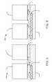
- FIG. 1is a diagram illustrating a side view of a conventional embodiment of a MEMS structure without shielding.
- FIG. 2is a diagram illustrating a side view of a MEMS structure with full shielding according to an embodiment of the present invention.
- FIG. 3is a simplified diagram illustrating a side view of a MEMS structure with single-sided partial shielding according to an embodiment of the present invention.
- FIG. 4is a simplified diagram illustrating a side view of a MEMS structure with full shielding and retrograde isolation according to an embodiment of the present invention.
- FIG. 5is a simplified flow diagram illustrating a method for fabricating a MEMS structure with full shielding and retrograde isolation according to an embodiment of the present invention.
- FIG. 6is a simplified diagram illustrating a cross-sectional view of an integrated MEMS-CMOS device according to an embodiment of the present invention.
- the present inventionis directed to MEMS (Micro-Electro-Mechanical-Systems). More specifically, embodiments of the invention provide methods and structure for improving integrated MEMS devices, including inertial sensors and the like.
- the MEMS devicecan include at least an accelerometer, a gyroscope, a magnetic sensor, a pressure sensor, a microphone, a humidity sensor, a temperature sensor, a chemical sensor, a biosensor, an inertial sensor, and others. But it will be recognized that the invention has a much broader range of applicability.
- FIGS. 1-4use the numerals listed in the following table:
- Movable structure layere.g. Si, poly-Si
- Anchored structure layere.g. Si, poly-Si
- Bottom isolation layere.g. SiO2, Si3N4
- Top isolation layere.g. SiO2, Si3N4
- Bottom edges of structure layer6
- Shielding layere.g. Al, poly-Si 8 Edge of the shielding layer 3a Exposed bottom isolation layer 3b Isolative path of Embodiment 1 3c Isolative path of Embodiment 2 7a Exposed shielding layer
- FIG. 1is a diagram illustrating a side view of a conventional embodiment of a MEMS structure without shielding.
- a MEMS structure 100having a movable structure layer 1 and an anchored structure layer 2 disposed overlying a bottom isolation layer 3 .
- the anchored structure layer 2is coupled to top isolation layer 4 , which is also coupled to the bottom isolation layer 3 .
- top isolation layer 4which is also coupled to the bottom isolation layer 3 .
- the exposed portion of the bottom isolation layer 3 a, the bottom edges 5 of the structure layers 1 and 2 , and the side walls 6 of the top isolation layer 4are shown. This configuration results in structural damage at the bottom edges 5 due to back-etching induced by accumulated charging at the exposed bottom isolation layer 3 a during an over-etching stage of the structure layers 1 and 2 .
- FIG. 2is a diagram illustrating a side view of a MEMS structure with full shielding according to an embodiment of the present invention.
- MEMS structure 200additionally has a shielding layer 7 , which is grounded, to prevent the charging at the exposed bottom layer.
- this configurationresults in a leakage path at the sidewalls 6 of the top isolation layer 4 between the anchored structure layer 2 and the shielding layer 7 .
- the leakage pathis due to the back-sputtering induced by plasma bombardments at the exposed shielding layer 7 a during an over-etching stage of the structure layers 1 and 2 , which deposits conductive shielding materials at adjacent sidewalls 6 of the top isolation layer 4 and bottoms of the structure layers 1 and 2 .
- some residue of a plasma etching processcan splash up on sidewalls 6 and can intermittently cause a short in the region between structure layer 2 and the shielding layer 7 .
- FIG. 3is a simplified diagram illustrating a side view of a MEMS structure with single-sided partial shielding according to an embodiment of the present invention.
- the shielding layer 7is configured such that it does not reach the sidewall 6 of the top isolation layer.
- This configurationprovides protection from charging and provides an isolative path ( 3 b ) between the edges 8 of the shielding 7 and the sidewalls 6 of the top isolation layer 4 .
- This isolation pathprovides isolation without back-sputtered materials.
- plasmawill still short to the shielding 7 and region 3 b still be protected from plasma damage.
- By reducing the shielding layer 7no residue will be splashed onto sidewall 6 .
- FIG. 4is a simplified diagram illustrating a side view of a MEMS structure with full shielding and retrograde isolation according to an embodiment of the present invention.
- This embodimentuses shielding layer 7 similar to that shown in FIG. 2 , however, the top isolation layer is cut back, through an etching process or the like. As an example, plasma residue and/or other materials will not stick to the sidewall 6 , and the MEMS device will not intermittently short out.
- FIG. 5is a simplified flow diagram illustrating a method for fabricating a MEMS structure with full shielding and retrograde isolation according to an embodiment of the present invention. Referring to FIG. 5 , an example of a manufacturing process 500 can be briefly described below:
- steps or a stepcan be added, removed, combined, reordered, or replaced, or has other variations, alternatives, and modifications. Further details of the present manufacturing process can be found throughout the present specification, and more particularly below.
- the methodbegins with providing a substrate member having a surface region.
- This substrate membercan include silicon materials, such as single crystal and polycrystalline silicon.
- the methodcan include forming a CMOS IC layer overlying the surface region, with the CMOS IC layer having at least one CMOS device.
- a bottom isolation layercan be formed overlying the CMOS IC layer and a shielding layer can be formed overlying a portion of the bottom isolation layer.
- the shielding layercan be formed within a portion of the bottom isolation layer.
- the methodcan include forming a top isolation layer overlying a portion of the bottom isolation layer.
- the bottom isolation layercan include an isolation region configured between the top isolation layer and the shielding layer.
- the isolation regionis an exposed portion of the bottom isolation layer free from contact with the top isolation layer and the shielding layer.
- a MEMS layercan be formed overlying the top isolation layer, the shielding layer, and the bottom isolation layer.
- the MEMS layercan be etched to form at least one MEMS structure having at least one movable structure and at least one anchored structure.
- the etching processcan include a plasma etching, a deep reactive-ion etching (DRIE), or other like process.
- the at least one anchored structurecan be coupled to a portion of the top isolation layer and the at least one movable structure is formed overlying the shielding layer.
- This MEMS structurecan include an accelerometer, a gyrometer, a magnetometer, a pressure sensor, or the like.
- the shielding layercan include a polysilicon, aluminum, or other like materials.
- the movable structure and anchored structure layerscan include silicon, polysilicon, or other like materials.
- the top and bottom isolation layerscan include silicon dioxide, silicon nitride, or other like materials.
- the shielding layercan include aluminum, polysilicon, or other like materials.
- the shielding layercan include a shielding layer having a single sided partial shielding layer underlying at least a portion of the movable structure. This configuration is similar to the embodiment shown in FIG. 3 .
- the shielding layercan include a full shielding layer underlying at least a portion of the movable structure and at least a portion of the anchored structure.
- the methodcan further include etching the top isolation layer to form the isolation region between the top isolation layer and the bottom isolation layer. This configuration is similar to the embodiment shown in FIG. 4 .
- embodiments of the present techniqueprovide an easy to use process to integrated MEMS and CMOS circuits on a single die.
- the methodprovides a fabrication process that protects exposed CMOS ICs from PID, leakage path, and other damage issues. Additionally, the method provides a process and system that are compatible with conventional semiconductor and MEMS process technologies without substantial modifications to conventional equipment and processes. Depending upon the embodiment, one or more of these benefits may be achieved.
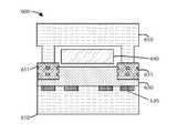
- FIG. 6is a simplified diagram illustrating a cross-sectional view of an integrated MEMS-CMOS device according to an embodiment of the present invention.
- This device 600includes a fully processed CMOS substrate 610 with CMOS circuits 620 .
- An oxide layer 630 and a MEMS structure 640overly the CMOS substrate 610 .
- a cap structure 650encapsulates the MEMS structure 640 .
- the region where the cap structure 650 meets the oxide layer 630is configured with metal stress buffers 631 .
- a metal stress buffer 631is provided underlying the contact regions of the cap. This arrangement has the advantages of reducing the risk of stress-induced oxide crack and circuit damages.
Landscapes
- Engineering & Computer Science (AREA)
- Microelectronics & Electronic Packaging (AREA)
- Manufacturing & Machinery (AREA)
- Computer Hardware Design (AREA)
- Health & Medical Sciences (AREA)
- General Health & Medical Sciences (AREA)
- Toxicology (AREA)
- Pressure Sensors (AREA)
- Micromachines (AREA)
Abstract
Description
- The present application claims priority to and incorporates by reference, for all purposes, the following pending provisional application: U.S. Provisional App. No. 61/835,510, filed Jun. 14, 2013. The present application also incorporates by reference, for all purposes, the following pending patent applications: U.S. patent application Ser. No. 13/788,503, filed Mar. 7, 2013.
- The present invention is directed to MEMS (Micro-Electro-Mechanical-Systems). More specifically, embodiments of the invention provide methods and structure for improving MEMS devices, including inertial sensors and the like. Merely by way of example, the MEMS device can include at least an accelerometer, a gyroscope, a magnetic sensor, a pressure sensor, a microphone, a humidity sensor, a temperature sensor, a chemical sensor, a biosensor, an inertial sensor, and others. But it will be recognized that the invention has a much broader range of applicability.
- Research and development in integrated microelectronics have continued to produce astounding progress in CMOS and MEMS. CMOS technology has become the predominant fabrication technology for integrated circuits (IC). MEMS, however, continues to rely upon conventional process technologies. In layman's terms, microelectronic ICs are the “brains” of an integrated device which provides decision-making capabilities, whereas MEMS are the “eyes” and “arms” that provide the ability to sense and control the environment. Some examples of the widespread application of these technologies are the switches in radio frequency (RF) antenna systems, such as those in the iPhone™ device by Apple, Inc. of Cupertino, Calif., and the Blackberry™ phone by Research In Motion Limited of Waterloo, Ontario, Canada, and accelerometers in sensor-equipped game devices, such as those in the Wii™ controller manufactured by Nintendo Company Limited of Japan. Though they are not always easily identifiable, these technologies are becoming ever more prevalent in society every day.
- Beyond consumer electronics, use of IC and MEMS has limitless applications through modular measurement devices such as accelerometers, gyroscopes, actuators, and sensors. In conventional vehicles, accelerometers and gyroscopes are used to deploy airbags and trigger dynamic stability control functions, respectively. MEMS gyroscopes can also be used for image stabilization systems in video and still cameras, and automatic steering systems in airplanes and torpedoes. Biological MEMS (Bio-MEMS) implement biosensors and chemical sensors for Lab-On-Chip applications, which integrate one or more laboratory functions on a single millimeter-sized chip only. Other applications include Internet and telephone networks, security and financial applications, and health care and medical systems. As described previously, ICs and MEMS can be used to practically engage in various type of environmental interaction.
- Although highly successful, ICs and in particular MEMS still have limitations. Similar to IC development, MEMS development, which focuses on increasing performance, reducing size, and decreasing cost, continues to be challenging. Additionally, applications of MEMS often require increasingly complex microsystems that desire greater computational power. Unfortunately, such applications generally do not exist. These and other limitations of conventional MEMS and ICs may be further described throughout the present specification and more particularly below.
- From the above, it is seen that techniques for improving MEMS structures are highly desired.
- The present invention is directed to MEMS (Micro-Electro-Mechanical-Systems). More specifically, embodiments of the invention provide methods and structure for improving MEMS devices, including inertial sensors and the like. Merely by way of example, the MEMS device can include at least an accelerometer, a gyroscope, a gyrometer, a magnetic field sensor, a pressure sensor, a microphone, a humidity sensor, a temperature sensor, a chemical sensor, a biosensor, an inertial sensor, and others. But it will be recognized that the invention has a much broader range of applicability.
- In an embodiment, the present method uses a micro-fabrication process that realizes moving mechanical structures (MEMS) on top of a conventional CMOS structure by bonding a mechanical structural wafer on top of the CMOS and etching the mechanical layer using plasma etching processes, such as Deep Reactive Ion Etching (DRIE). During etching of the mechanical layer, CMOS devices that are directly connected to the mechanical layer are exposed to plasma. This sometimes causes permanent damage to CMOS circuits and is termed Plasma Induced Damage (PID). An object of the present invention is to prevent or reduce this PID and protect the underlying CMOS circuits by grounding and providing an alternate path for the CMOS circuits until the MEMS layer is completely etched.
- In an embodiment, the present invention can include a method for fabricating an integrated MEMS-CMOS device. The method can include providing a substrate member having a surface region and forming a CMOS IC layer having at least one CMOS device overlying the surface region. A bottom isolation layer can be formed overlying the CMOS IC layer and a shielding layer and a top isolation layer can be formed overlying a portion of bottom isolation layer. The bottom isolation layer can include an isolation region between the top isolation layer and the shielding layer. A MEMS layer overlying the top isolation layer, the shielding layer, and the bottom isolation layer, and can be etched to form at least one MEMS structure having at least one movable structure and at least one anchored structure, wherein the at least one anchored structure is coupled to a portion of the top isolation layer, wherein the at least one movable structure is formed overlying the shielding layer.
- Many benefits are achieved by way of embodiments of the present invention over conventional techniques. For example, embodiments of the present technique provide an easy to use process to integrated MEMS and CMOS circuits on a single die. In some embodiments, the method provides a fabrication process that protects exposed CMOS ICs from PID, leakage path, and other damage issues. Additionally, the method provides a process and system that are compatible with conventional semiconductor and MEMS process technologies without substantial modifications to conventional equipment and processes. Depending upon the embodiment, one or more of these benefits may be achieved. These and other benefits will be described in more detail throughout the present specification and more particularly below.
- Various additional objects, features and advantages of the present invention can be more fully appreciated with reference to the detailed description and accompanying drawings that follow.
- In order to more fully understand the present invention, reference is made to the accompanying drawings. Understanding that these drawings are not to be considered limitations in the scope of the invention, the presently described embodiments and the presently understood best mode of the invention are described with additional detail through use of the accompanying drawings in which:
FIG. 1 is a diagram illustrating a side view of a conventional embodiment of a MEMS structure without shielding.FIG. 2 is a diagram illustrating a side view of a MEMS structure with full shielding according to an embodiment of the present invention.FIG. 3 is a simplified diagram illustrating a side view of a MEMS structure with single-sided partial shielding according to an embodiment of the present invention.FIG. 4 is a simplified diagram illustrating a side view of a MEMS structure with full shielding and retrograde isolation according to an embodiment of the present invention.FIG. 5 is a simplified flow diagram illustrating a method for fabricating a MEMS structure with full shielding and retrograde isolation according to an embodiment of the present invention.FIG. 6 is a simplified diagram illustrating a cross-sectional view of an integrated MEMS-CMOS device according to an embodiment of the present invention.- The present invention is directed to MEMS (Micro-Electro-Mechanical-Systems). More specifically, embodiments of the invention provide methods and structure for improving integrated MEMS devices, including inertial sensors and the like. Merely by way of example, the MEMS device can include at least an accelerometer, a gyroscope, a magnetic sensor, a pressure sensor, a microphone, a humidity sensor, a temperature sensor, a chemical sensor, a biosensor, an inertial sensor, and others. But it will be recognized that the invention has a much broader range of applicability.
FIGS. 1-4 use the numerals listed in the following table:1 Movable structure layer (e.g. Si, poly-Si) 2 Anchored structure layer (e.g. Si, poly-Si) 3 Bottom isolation layer (e.g. SiO2, Si3N4) 4 Top isolation layer (e.g. SiO2, Si3N4) 5 Bottom edges of structure layer 6 Sidewalls of top isolation layer 7 Shielding layer (e.g. Al, poly-Si) 8 Edge of the shielding layer 3a Exposed bottom isolation layer 3b Isolative path of Embodiment 13c Isolative path of Embodiment 27a Exposed shielding layer FIG. 1 is a diagram illustrating a side view of a conventional embodiment of a MEMS structure without shielding. As shown, aMEMS structure 100 having amovable structure layer 1 and an anchoredstructure layer 2 disposed overlying abottom isolation layer 3. The anchoredstructure layer 2 is coupled totop isolation layer 4, which is also coupled to thebottom isolation layer 3. For reference, the exposed portion of thebottom isolation layer 3a,thebottom edges 5 of the structure layers1 and2, and theside walls 6 of thetop isolation layer 4 are shown. This configuration results in structural damage at thebottom edges 5 due to back-etching induced by accumulated charging at the exposedbottom isolation layer 3aduring an over-etching stage of the structure layers1 and2.FIG. 2 is a diagram illustrating a side view of a MEMS structure with full shielding according to an embodiment of the present invention. Compared toMEMS structure 100,MEMS structure 200 additionally has ashielding layer 7, which is grounded, to prevent the charging at the exposed bottom layer. However, this configuration results in a leakage path at thesidewalls 6 of thetop isolation layer 4 between the anchoredstructure layer 2 and theshielding layer 7. The leakage path is due to the back-sputtering induced by plasma bombardments at the exposedshielding layer 7aduring an over-etching stage of the structure layers1 and2, which deposits conductive shielding materials atadjacent sidewalls 6 of thetop isolation layer 4 and bottoms of the structure layers1 and2. As an example, some residue of a plasma etching process can splash up onsidewalls 6 and can intermittently cause a short in the region betweenstructure layer 2 and theshielding layer 7.FIG. 3 is a simplified diagram illustrating a side view of a MEMS structure with single-sided partial shielding according to an embodiment of the present invention. In this embodiment, theshielding layer 7 is configured such that it does not reach thesidewall 6 of the top isolation layer. This configuration provides protection from charging and provides an isolative path (3b) between theedges 8 of the shielding7 and thesidewalls 6 of thetop isolation layer 4. This isolation path provides isolation without back-sputtered materials. As an example, plasma will still short to theshielding 7 andregion 3bstill be protected from plasma damage. By reducing theshielding layer 7, no residue will be splashed ontosidewall 6.FIG. 4 is a simplified diagram illustrating a side view of a MEMS structure with full shielding and retrograde isolation according to an embodiment of the present invention. This embodiment uses shieldinglayer 7 similar to that shown inFIG. 2 , however, the top isolation layer is cut back, through an etching process or the like. As an example, plasma residue and/or other materials will not stick to thesidewall 6, and the MEMS device will not intermittently short out.FIG. 5 is a simplified flow diagram illustrating a method for fabricating a MEMS structure with full shielding and retrograde isolation according to an embodiment of the present invention. Referring toFIG. 5 , an example of amanufacturing process 500 can be briefly described below:- 1. Start; (step502)
- 2. Provide a substrate member having a surface region; (step504)
- 3. Form a CMOS IC layer overlying the surface region, the CMOS IC layer having at least one CMOS device; (step506)
- 4. Form a bottom isolation layer overlying the CMOS IC layer; step (508)
- 5. Form a shielding layer overlying a portion of the bottom isolation layer; (step510)
- 6. Form a top isolation layer overlying a portion of the bottom isolation layer, wherein the bottom isolation layer includes an isolation region between the top isolation layer and the shielding layer; (step512)
- 7. Form a MEMS layer overlying the top isolation layer, the shielding layer, and the bottom isolation layer; (step514)
- 8. Etch the MEMS layer to form at least one MEMS structure having at least one movable structure and at least one anchored structure, wherein the at least one anchored structure is coupled to a portion of the top isolation layer, wherein the at least one movable structure is formed overlying the shielding layer; (step516) and
- 9. Perform other steps, as desired. (step518)
- The aforementioned steps are provided for the formation of an integrated MEMS-CMOS device using an improved shielding configuration. Of course, depending upon the embodiment, steps or a step can be added, removed, combined, reordered, or replaced, or has other variations, alternatives, and modifications. Further details of the present manufacturing process can be found throughout the present specification, and more particularly below.
- As shown in
FIG. 5 , the method begins with providing a substrate member having a surface region. This substrate member can include silicon materials, such as single crystal and polycrystalline silicon. The method can include forming a CMOS IC layer overlying the surface region, with the CMOS IC layer having at least one CMOS device. A bottom isolation layer can be formed overlying the CMOS IC layer and a shielding layer can be formed overlying a portion of the bottom isolation layer. In a specific embodiment, the shielding layer can be formed within a portion of the bottom isolation layer. - In an embodiment, the method can include forming a top isolation layer overlying a portion of the bottom isolation layer. The bottom isolation layer can include an isolation region configured between the top isolation layer and the shielding layer. In an embodiment, the isolation region is an exposed portion of the bottom isolation layer free from contact with the top isolation layer and the shielding layer. A MEMS layer can be formed overlying the top isolation layer, the shielding layer, and the bottom isolation layer.
- The MEMS layer can be etched to form at least one MEMS structure having at least one movable structure and at least one anchored structure. In a specific embodiment, the etching process can include a plasma etching, a deep reactive-ion etching (DRIE), or other like process. The at least one anchored structure can be coupled to a portion of the top isolation layer and the at least one movable structure is formed overlying the shielding layer. This MEMS structure can include an accelerometer, a gyrometer, a magnetometer, a pressure sensor, or the like.
- In a specific embodiment, the shielding layer can include a polysilicon, aluminum, or other like materials. The movable structure and anchored structure layers can include silicon, polysilicon, or other like materials. The top and bottom isolation layers can include silicon dioxide, silicon nitride, or other like materials. The shielding layer can include aluminum, polysilicon, or other like materials. Those of ordinary skill in the art will recognize other variations, modifications, and alternatives.
- In a specific embodiment, the shielding layer can include a shielding layer having a single sided partial shielding layer underlying at least a portion of the movable structure. This configuration is similar to the embodiment shown in
FIG. 3 . - In a specific embodiment, the shielding layer can include a full shielding layer underlying at least a portion of the movable structure and at least a portion of the anchored structure. In this embodiment, the method can further include etching the top isolation layer to form the isolation region between the top isolation layer and the bottom isolation layer. This configuration is similar to the embodiment shown in
FIG. 4 . - Many benefits are achieved by way of embodiments of the present invention over conventional techniques. For example, embodiments of the present technique provide an easy to use process to integrated MEMS and CMOS circuits on a single die. In some embodiments, the method provides a fabrication process that protects exposed CMOS ICs from PID, leakage path, and other damage issues. Additionally, the method provides a process and system that are compatible with conventional semiconductor and MEMS process technologies without substantial modifications to conventional equipment and processes. Depending upon the embodiment, one or more of these benefits may be achieved.
FIG. 6 is a simplified diagram illustrating a cross-sectional view of an integrated MEMS-CMOS device according to an embodiment of the present invention. Thisdevice 600 includes a fully processedCMOS substrate 610 withCMOS circuits 620. Anoxide layer 630 and aMEMS structure 640 overly theCMOS substrate 610. Acap structure 650 encapsulates theMEMS structure 640. The region where thecap structure 650 meets theoxide layer 630 is configured with metal stress buffers631. Here, ametal stress buffer 631 is provided underlying the contact regions of the cap. This arrangement has the advantages of reducing the risk of stress-induced oxide crack and circuit damages.- It is also understood that the examples and embodiments described herein are for illustrative purposes only and that various modifications or changes in light thereof will be suggested to persons skilled in the art and are to be included within the spirit and purview of this application and scope of the appended claims.
Claims (20)
Priority Applications (3)
| Application Number | Priority Date | Filing Date | Title |
|---|---|---|---|
| US14/302,385US10046964B2 (en) | 2013-03-07 | 2014-06-11 | MEMS structure with improved shielding and method |
| TW103120608ATWI579229B (en) | 2013-06-14 | 2014-06-13 | A mems structure with improved shielding and method |
| US14/930,642US9950921B2 (en) | 2013-03-07 | 2015-11-02 | MEMS structure with improved shielding and method |
Applications Claiming Priority (3)
| Application Number | Priority Date | Filing Date | Title |
|---|---|---|---|
| US13/788,503US9276080B2 (en) | 2012-03-09 | 2013-03-07 | Methods and structures of integrated MEMS-CMOS devices |
| US201361835510P | 2013-06-14 | 2013-06-14 | |
| US14/302,385US10046964B2 (en) | 2013-03-07 | 2014-06-11 | MEMS structure with improved shielding and method |
Related Child Applications (1)
| Application Number | Title | Priority Date | Filing Date |
|---|---|---|---|
| US14/930,642ContinuationUS9950921B2 (en) | 2013-03-07 | 2015-11-02 | MEMS structure with improved shielding and method |
Publications (2)
| Publication Number | Publication Date |
|---|---|
| US20140370638A1true US20140370638A1 (en) | 2014-12-18 |
| US10046964B2 US10046964B2 (en) | 2018-08-14 |
Family
ID=52019558
Family Applications (2)
| Application Number | Title | Priority Date | Filing Date |
|---|---|---|---|
| US14/302,385ActiveUS10046964B2 (en) | 2013-03-07 | 2014-06-11 | MEMS structure with improved shielding and method |
| US14/930,642ActiveUS9950921B2 (en) | 2013-03-07 | 2015-11-02 | MEMS structure with improved shielding and method |
Family Applications After (1)
| Application Number | Title | Priority Date | Filing Date |
|---|---|---|---|
| US14/930,642ActiveUS9950921B2 (en) | 2013-03-07 | 2015-11-02 | MEMS structure with improved shielding and method |
Country Status (2)
| Country | Link |
|---|---|
| US (2) | US10046964B2 (en) |
| TW (1) | TWI579229B (en) |
Cited By (12)
| Publication number | Priority date | Publication date | Assignee | Title |
|---|---|---|---|---|
| US9309106B2 (en) | 2013-07-08 | 2016-04-12 | Motion Engine Inc. | 3D MEMS device and method of manufacturing |
| US9950921B2 (en) | 2013-03-07 | 2018-04-24 | MCube Inc. | MEMS structure with improved shielding and method |
| US10145906B2 (en) | 2015-12-17 | 2018-12-04 | Analog Devices Global | Devices, systems and methods including magnetic structures |
| US10214414B2 (en) | 2014-01-09 | 2019-02-26 | Motion Engine, Inc. | Integrated MEMS system |
| US10273147B2 (en) | 2013-07-08 | 2019-04-30 | Motion Engine Inc. | MEMS components and method of wafer-level manufacturing thereof |
| US10407299B2 (en) | 2015-01-15 | 2019-09-10 | Motion Engine Inc. | 3D MEMS device with hermetic cavity |
| US10551215B2 (en) | 2015-06-11 | 2020-02-04 | Analog Devices Global Unlimited Company | Systems, circuits and methods for determining a position of a movable object |
| US10768065B2 (en) | 2014-04-10 | 2020-09-08 | Mei Micro, Inc. | MEMS pressure sensor |
| US11084713B2 (en)* | 2018-09-27 | 2021-08-10 | Taiwan Semiconductor Manufacturing Company, Ltd. | Bypass structure |
| US11287486B2 (en) | 2014-12-09 | 2022-03-29 | Motion Engine, Inc. | 3D MEMS magnetometer and associated methods |
| US11674803B2 (en) | 2014-06-02 | 2023-06-13 | Motion Engine, Inc. | Multi-mass MEMS motion sensor |
| US11852481B2 (en) | 2013-08-02 | 2023-12-26 | Motion Engine Inc. | MEMS motion sensor and method of manufacturing |
Citations (4)
| Publication number | Priority date | Publication date | Assignee | Title |
|---|---|---|---|---|
| US20050249966A1 (en)* | 2004-05-04 | 2005-11-10 | Ming-Hau Tung | Method of manufacture for microelectromechanical devices |
| US20100237738A1 (en)* | 2009-03-17 | 2010-09-23 | Charles Gordon Smith | Moving a free-standing structure between high and low adhesion states |
| US20130140155A1 (en)* | 2011-02-14 | 2013-06-06 | Ilkka Urvas | MEMS Switch Having Cantilevered Actuation |
| US20130299925A1 (en)* | 2012-05-14 | 2013-11-14 | Robert Bosch Gmbh | Micromechanical inertial sensor and method for manufacturing same |
Family Cites Families (40)
| Publication number | Priority date | Publication date | Assignee | Title |
|---|---|---|---|---|
| US5825385A (en) | 1995-04-12 | 1998-10-20 | Eastman Kodak Company | Constructions and manufacturing processes for thermally activated print heads |
| US5736732A (en) | 1996-12-23 | 1998-04-07 | General Electric Company | Induced charge prevention in semiconductor imaging devices |
| US6725719B2 (en) | 2002-04-17 | 2004-04-27 | Milli Sensor Systems And Actuators, Inc. | MEMS-integrated inertial measurement units on a common substrate |
| US7122395B2 (en) | 2002-12-23 | 2006-10-17 | Motorola, Inc. | Method of forming semiconductor devices through epitaxy |
| EP1904398A2 (en)* | 2005-06-30 | 2008-04-02 | Philips Intellectual Property & Standards GmbH | A method of manufacturing a mems element |
| US20080116534A1 (en) | 2006-11-17 | 2008-05-22 | Charles Grosjean | Substrate contact for a MEMS device |
| US20100071467A1 (en) | 2008-09-24 | 2010-03-25 | Invensense | Integrated multiaxis motion sensor |
| US7923790B1 (en) | 2007-03-09 | 2011-04-12 | Silicon Laboratories Inc. | Planar microshells for vacuum encapsulated devices and damascene method of manufacture |
| US7595209B1 (en) | 2007-03-09 | 2009-09-29 | Silicon Clocks, Inc. | Low stress thin film microshells |
| US7821046B2 (en) | 2007-04-27 | 2010-10-26 | Aptina Imaging Corporation | Methods, structures and sytems for an image sensor device for improving quantum efficiency of red pixels |
| US7745892B1 (en)* | 2007-12-13 | 2010-06-29 | Rf Micro Devices, Inc. | Integrated MEMS switch |
| US7800190B2 (en) | 2008-06-16 | 2010-09-21 | Honeywell International Inc. | Getter on die in an upper sense plate designed system |
| US8939029B2 (en) | 2008-09-05 | 2015-01-27 | Analog Devices, Inc. | MEMS sensor with movable Z-axis sensing element |
| CN101393321B (en) | 2008-10-09 | 2010-06-02 | 重庆大学 | Monolithic integration method of grating optical modulator and active matrix driving circuit |
| TW201020548A (en) | 2008-11-18 | 2010-06-01 | Ind Tech Res Inst | Multi-axis capacitive accelerometer |
| US8205498B2 (en) | 2008-11-18 | 2012-06-26 | Industrial Technology Research Institute | Multi-axis capacitive accelerometer |
| US8445306B2 (en)* | 2008-12-24 | 2013-05-21 | International Business Machines Corporation | Hybrid MEMS RF switch and method of fabricating same |
| GB2467776A (en) | 2009-02-13 | 2010-08-18 | Wolfson Microelectronics Plc | Integrated MEMS transducer and circuitry |
| TWI411064B (en) | 2009-03-16 | 2013-10-01 | 松下電器產業股份有限公司 | Microelectromechanical system |
| CN102439719B (en) | 2009-05-14 | 2015-06-24 | 高通股份有限公司 | System-in packages |
| US8823007B2 (en) | 2009-10-28 | 2014-09-02 | MCube Inc. | Integrated system on chip using multiple MEMS and CMOS devices |
| US8710599B2 (en) | 2009-08-04 | 2014-04-29 | Fairchild Semiconductor Corporation | Micromachined devices and fabricating the same |
| TWI433809B (en)* | 2009-12-09 | 2014-04-11 | Nat Chip Implementation Ct Nat Applied Res Lab | CMOS microelectromechanical cantilever structure |
| US8516886B2 (en) | 2010-04-30 | 2013-08-27 | Qualcomm Mems Technologies, Inc. | Micromachined piezoelectric X-Axis gyroscope |
| JP5527019B2 (en) | 2010-05-28 | 2014-06-18 | セイコーエプソン株式会社 | Physical quantity sensor and electronic equipment |
| US8487398B2 (en) | 2010-07-14 | 2013-07-16 | Freescale Semiconductor, Inc. | Capacitor device using an isolated well and method therefor |
| CN103221778B (en) | 2010-09-18 | 2016-03-30 | 快捷半导体公司 | There is single micromechanics one chip three-axis gyroscope driven |
| US9540232B2 (en) | 2010-11-12 | 2017-01-10 | MCube Inc. | Method and structure of MEMS WLCSP fabrication |
| US9276080B2 (en) | 2012-03-09 | 2016-03-01 | Mcube, Inc. | Methods and structures of integrated MEMS-CMOS devices |
| JP2014504364A (en) | 2010-12-08 | 2014-02-20 | マイクロファイン・マテリアルズ・テクノロジーズ・ピーティーイー・リミテッド | High performance curved accelerometer |
| US8878312B2 (en) | 2011-03-01 | 2014-11-04 | Taiwan Semiconductor Manufacturing Company, Ltd. | Electrical bypass structure for MEMS device |
| US8754529B2 (en) | 2011-03-28 | 2014-06-17 | Miradia, Inc. | MEMS device with simplified electrical conducting paths |
| US9540230B2 (en) | 2011-06-27 | 2017-01-10 | Invensense, Inc. | Methods for CMOS-MEMS integrated devices with multiple sealed cavities maintained at various pressures |
| US20130042686A1 (en) | 2011-08-17 | 2013-02-21 | Sitronix Technology Corp. | Inertia sensing apparatus |
| US8836055B2 (en) | 2011-09-30 | 2014-09-16 | Taiwan Semiconductor Manufacturing Company, Ltd. | MEMS structures and methods for forming the same |
| US9249012B2 (en) | 2013-01-25 | 2016-02-02 | Mcube, Inc. | Method and device of MEMS process control monitoring and packaged MEMS with different cavity pressures |
| US10036635B2 (en) | 2013-01-25 | 2018-07-31 | MCube Inc. | Multi-axis MEMS rate sensor device |
| US10132630B2 (en) | 2013-01-25 | 2018-11-20 | MCube Inc. | Multi-axis integrated MEMS inertial sensing device on single packaged chip |
| US10046964B2 (en) | 2013-03-07 | 2018-08-14 | MCube Inc. | MEMS structure with improved shielding and method |
| US9075079B2 (en) | 2013-03-07 | 2015-07-07 | MCube Inc. | Method and structure of an integrated MEMS inertial sensor device using electrostatic quadrature-cancellation |
- 2014
- 2014-06-11USUS14/302,385patent/US10046964B2/enactiveActive
- 2014-06-13TWTW103120608Apatent/TWI579229B/enactive
- 2015
- 2015-11-02USUS14/930,642patent/US9950921B2/enactiveActive
Patent Citations (4)
| Publication number | Priority date | Publication date | Assignee | Title |
|---|---|---|---|---|
| US20050249966A1 (en)* | 2004-05-04 | 2005-11-10 | Ming-Hau Tung | Method of manufacture for microelectromechanical devices |
| US20100237738A1 (en)* | 2009-03-17 | 2010-09-23 | Charles Gordon Smith | Moving a free-standing structure between high and low adhesion states |
| US20130140155A1 (en)* | 2011-02-14 | 2013-06-06 | Ilkka Urvas | MEMS Switch Having Cantilevered Actuation |
| US20130299925A1 (en)* | 2012-05-14 | 2013-11-14 | Robert Bosch Gmbh | Micromechanical inertial sensor and method for manufacturing same |
Cited By (17)
| Publication number | Priority date | Publication date | Assignee | Title |
|---|---|---|---|---|
| US9950921B2 (en) | 2013-03-07 | 2018-04-24 | MCube Inc. | MEMS structure with improved shielding and method |
| US9309106B2 (en) | 2013-07-08 | 2016-04-12 | Motion Engine Inc. | 3D MEMS device and method of manufacturing |
| US10273147B2 (en) | 2013-07-08 | 2019-04-30 | Motion Engine Inc. | MEMS components and method of wafer-level manufacturing thereof |
| US11852481B2 (en) | 2013-08-02 | 2023-12-26 | Motion Engine Inc. | MEMS motion sensor and method of manufacturing |
| US10214414B2 (en) | 2014-01-09 | 2019-02-26 | Motion Engine, Inc. | Integrated MEMS system |
| US10768065B2 (en) | 2014-04-10 | 2020-09-08 | Mei Micro, Inc. | MEMS pressure sensor |
| US11579033B2 (en) | 2014-04-10 | 2023-02-14 | Mei Micro, Inc. | MEMS pressure sensor |
| US11674803B2 (en) | 2014-06-02 | 2023-06-13 | Motion Engine, Inc. | Multi-mass MEMS motion sensor |
| US11287486B2 (en) | 2014-12-09 | 2022-03-29 | Motion Engine, Inc. | 3D MEMS magnetometer and associated methods |
| US10407299B2 (en) | 2015-01-15 | 2019-09-10 | Motion Engine Inc. | 3D MEMS device with hermetic cavity |
| US10551215B2 (en) | 2015-06-11 | 2020-02-04 | Analog Devices Global Unlimited Company | Systems, circuits and methods for determining a position of a movable object |
| US10429456B2 (en) | 2015-12-17 | 2019-10-01 | Analog Devices Global | Modules and methods including magnetic sensing structures |
| US11061086B2 (en) | 2015-12-17 | 2021-07-13 | Analog Devices Global | Magnetic device with magnetic structure and micro-fluidic structure |
| US11649157B2 (en) | 2015-12-17 | 2023-05-16 | Analog Devices International Unlimited Company | Devices, systems and methods including magnetic structures and micromechanical structure |
| US10145906B2 (en) | 2015-12-17 | 2018-12-04 | Analog Devices Global | Devices, systems and methods including magnetic structures |
| US11084713B2 (en)* | 2018-09-27 | 2021-08-10 | Taiwan Semiconductor Manufacturing Company, Ltd. | Bypass structure |
| US12297097B2 (en) | 2018-09-27 | 2025-05-13 | Taiwan Semiconductor Manufacturing Company, Ltd. | Bypass structure |
Also Published As
| Publication number | Publication date |
|---|---|
| TW201504134A (en) | 2015-02-01 |
| US9950921B2 (en) | 2018-04-24 |
| US10046964B2 (en) | 2018-08-14 |
| TWI579229B (en) | 2017-04-21 |
| US20160052777A1 (en) | 2016-02-25 |
Similar Documents
| Publication | Publication Date | Title |
|---|---|---|
| US9950921B2 (en) | MEMS structure with improved shielding and method | |
| US8367522B1 (en) | Method and structure of integrated micro electro-mechanical systems and electronic devices using edge bond pads | |
| US9365412B2 (en) | Integrated CMOS and MEMS devices with air dieletrics | |
| US8794065B1 (en) | Integrated inertial sensing apparatus using MEMS and quartz configured on crystallographic planes | |
| US9725304B2 (en) | Method to package multiple MEMS sensors and actuators at different gases and cavity pressures | |
| US9340414B2 (en) | Method and structure of monolithically integrated absolute pressure sensor | |
| KR102137103B1 (en) | An integration scheme for wafer level packaging | |
| US8093087B2 (en) | Method for fabricating MEMS device | |
| US9944516B2 (en) | High aspect ratio etch without upper widening | |
| US7851975B2 (en) | MEMS structure with metal protection rings | |
| US20150061046A1 (en) | Wafer level method of sealing different pressure levels for mems sensors | |
| US9725298B2 (en) | CMOS integrated moving-gate transducer with silicon as a functional layer | |
| US10131533B1 (en) | Microelectromechanical system device and method for manufacturing the same | |
| US8129805B2 (en) | Microelectromechanical system (MEMS) device and methods for fabricating the same | |
| US8584521B1 (en) | Accurate gyroscope device using MEMS and quartz | |
| US10913653B2 (en) | Method of fabricating MEMS devices using plasma etching and device therefor | |
| US9593008B2 (en) | MEMS sensor including an over-travel stop and method of manufacture | |
| US8564075B1 (en) | Package tolerate design and method | |
| CN107304039A (en) | A kind of semiconductor devices and preparation method thereof and electronic installation |
Legal Events
| Date | Code | Title | Description |
|---|---|---|---|
| AS | Assignment | Owner name:MCUBE INC., CALIFORNIA Free format text:ASSIGNMENT OF ASSIGNORS INTEREST;ASSIGNORS:LEE, TE-HSI TERRENCE;SRIDHARAMURTHY, SUDHEER;YONEOKA, SHINGO;AND OTHERS;SIGNING DATES FROM 20140612 TO 20140616;REEL/FRAME:033405/0871 | |
| STCF | Information on status: patent grant | Free format text:PATENTED CASE | |
| MAFP | Maintenance fee payment | Free format text:PAYMENT OF MAINTENANCE FEE, 4TH YR, SMALL ENTITY (ORIGINAL EVENT CODE: M2551); ENTITY STATUS OF PATENT OWNER: SMALL ENTITY Year of fee payment:4 | |
| AS | Assignment | Owner name:SILICON VALLEY BANK, CALIFORNIA Free format text:SECURITY INTEREST;ASSIGNOR:MOVELLA INC. (FKA MCUBE, INC.);REEL/FRAME:059147/0471 Effective date:20220225 | |
| AS | Assignment | Owner name:MOVELLA INC. (FORMERLY KNOWN AS MCUBE, INC.), CALIFORNIA Free format text:RELEASE BY SECURED PARTY;ASSIGNOR:SILICON VALLEY BANK;REEL/FRAME:061763/0864 Effective date:20221114 | |
| AS | Assignment | Owner name:WILMINGTON SAVINGS FUND SOCIETY, FSB, AS AGENT, DELAWARE Free format text:NOTICE OF GRANT OF SECURITY INTEREST IN PATENTS;ASSIGNOR:MOVELLA INC.;REEL/FRAME:061948/0764 Effective date:20221114 | |
| AS | Assignment | Owner name:MOVELLA INC., CALIFORNIA Free format text:PARTIAL TERMINATION AND RELEASE OF SECURITY INTEREST IN PATENTS AT REEL/FRAME NO. 61948/0764;ASSIGNOR:WILMINGTON SAVINGS FUND SOCIETY, FSB, AS AGENT;REEL/FRAME:071161/0930 Effective date:20250502 |