US20140367840A1 - Mold cap for semiconductor device - Google Patents
Mold cap for semiconductor deviceDownload PDFInfo
- Publication number
- US20140367840A1 US20140367840A1US13/917,641US201313917641AUS2014367840A1US 20140367840 A1US20140367840 A1US 20140367840A1US 201313917641 AUS201313917641 AUS 201313917641AUS 2014367840 A1US2014367840 A1US 2014367840A1
- Authority
- US
- United States
- Prior art keywords
- substrate
- extensions
- mold
- mold body
- semiconductor package
- Prior art date
- Legal status (The legal status is an assumption and is not a legal conclusion. Google has not performed a legal analysis and makes no representation as to the accuracy of the status listed.)
- Granted
Links
Images


Classifications
- H—ELECTRICITY
- H01—ELECTRIC ELEMENTS
- H01L—SEMICONDUCTOR DEVICES NOT COVERED BY CLASS H10
- H01L23/00—Details of semiconductor or other solid state devices
- H01L23/28—Encapsulations, e.g. encapsulating layers, coatings, e.g. for protection
- H01L23/31—Encapsulations, e.g. encapsulating layers, coatings, e.g. for protection characterised by the arrangement or shape
- H01L23/3107—Encapsulations, e.g. encapsulating layers, coatings, e.g. for protection characterised by the arrangement or shape the device being completely enclosed
- H01L23/3121—Encapsulations, e.g. encapsulating layers, coatings, e.g. for protection characterised by the arrangement or shape the device being completely enclosed a substrate forming part of the encapsulation
- H01L23/3128—Encapsulations, e.g. encapsulating layers, coatings, e.g. for protection characterised by the arrangement or shape the device being completely enclosed a substrate forming part of the encapsulation the substrate having spherical bumps for external connection
- H—ELECTRICITY
- H01—ELECTRIC ELEMENTS
- H01L—SEMICONDUCTOR DEVICES NOT COVERED BY CLASS H10
- H01L23/00—Details of semiconductor or other solid state devices
- H01L23/28—Encapsulations, e.g. encapsulating layers, coatings, e.g. for protection
- H01L23/31—Encapsulations, e.g. encapsulating layers, coatings, e.g. for protection characterised by the arrangement or shape
- H01L23/3107—Encapsulations, e.g. encapsulating layers, coatings, e.g. for protection characterised by the arrangement or shape the device being completely enclosed
- H—ELECTRICITY
- H01—ELECTRIC ELEMENTS
- H01L—SEMICONDUCTOR DEVICES NOT COVERED BY CLASS H10
- H01L23/00—Details of semiconductor or other solid state devices
- H01L23/02—Containers; Seals
- H01L23/04—Containers; Seals characterised by the shape of the container or parts, e.g. caps, walls
- H01L23/053—Containers; Seals characterised by the shape of the container or parts, e.g. caps, walls the container being a hollow construction and having an insulating or insulated base as a mounting for the semiconductor body
- H01L23/055—Containers; Seals characterised by the shape of the container or parts, e.g. caps, walls the container being a hollow construction and having an insulating or insulated base as a mounting for the semiconductor body the leads having a passage through the base
- H—ELECTRICITY
- H01—ELECTRIC ELEMENTS
- H01L—SEMICONDUCTOR DEVICES NOT COVERED BY CLASS H10
- H01L21/00—Processes or apparatus adapted for the manufacture or treatment of semiconductor or solid state devices or of parts thereof
- H01L21/02—Manufacture or treatment of semiconductor devices or of parts thereof
- H01L21/04—Manufacture or treatment of semiconductor devices or of parts thereof the devices having potential barriers, e.g. a PN junction, depletion layer or carrier concentration layer
- H01L21/50—Assembly of semiconductor devices using processes or apparatus not provided for in a single one of the groups H01L21/18 - H01L21/326 or H10D48/04 - H10D48/07 e.g. sealing of a cap to a base of a container
- H01L21/56—Encapsulations, e.g. encapsulation layers, coatings
- H01L21/565—Moulds
- H—ELECTRICITY
- H01—ELECTRIC ELEMENTS
- H01L—SEMICONDUCTOR DEVICES NOT COVERED BY CLASS H10
- H01L24/00—Arrangements for connecting or disconnecting semiconductor or solid-state bodies; Methods or apparatus related thereto
- H01L24/93—Batch processes
- H01L24/95—Batch processes at chip-level, i.e. with connecting carried out on a plurality of singulated devices, i.e. on diced chips
- H01L24/97—Batch processes at chip-level, i.e. with connecting carried out on a plurality of singulated devices, i.e. on diced chips the devices being connected to a common substrate, e.g. interposer, said common substrate being separable into individual assemblies after connecting
- H—ELECTRICITY
- H01—ELECTRIC ELEMENTS
- H01L—SEMICONDUCTOR DEVICES NOT COVERED BY CLASS H10
- H01L2224/00—Indexing scheme for arrangements for connecting or disconnecting semiconductor or solid-state bodies and methods related thereto as covered by H01L24/00
- H01L2224/01—Means for bonding being attached to, or being formed on, the surface to be connected, e.g. chip-to-package, die-attach, "first-level" interconnects; Manufacturing methods related thereto
- H01L2224/26—Layer connectors, e.g. plate connectors, solder or adhesive layers; Manufacturing methods related thereto
- H01L2224/31—Structure, shape, material or disposition of the layer connectors after the connecting process
- H01L2224/32—Structure, shape, material or disposition of the layer connectors after the connecting process of an individual layer connector
- H01L2224/321—Disposition
- H01L2224/32151—Disposition the layer connector connecting between a semiconductor or solid-state body and an item not being a semiconductor or solid-state body, e.g. chip-to-substrate, chip-to-passive
- H01L2224/32221—Disposition the layer connector connecting between a semiconductor or solid-state body and an item not being a semiconductor or solid-state body, e.g. chip-to-substrate, chip-to-passive the body and the item being stacked
- H01L2224/32225—Disposition the layer connector connecting between a semiconductor or solid-state body and an item not being a semiconductor or solid-state body, e.g. chip-to-substrate, chip-to-passive the body and the item being stacked the item being non-metallic, e.g. insulating substrate with or without metallisation
- H—ELECTRICITY
- H01—ELECTRIC ELEMENTS
- H01L—SEMICONDUCTOR DEVICES NOT COVERED BY CLASS H10
- H01L2224/00—Indexing scheme for arrangements for connecting or disconnecting semiconductor or solid-state bodies and methods related thereto as covered by H01L24/00
- H01L2224/01—Means for bonding being attached to, or being formed on, the surface to be connected, e.g. chip-to-package, die-attach, "first-level" interconnects; Manufacturing methods related thereto
- H01L2224/42—Wire connectors; Manufacturing methods related thereto
- H01L2224/47—Structure, shape, material or disposition of the wire connectors after the connecting process
- H01L2224/48—Structure, shape, material or disposition of the wire connectors after the connecting process of an individual wire connector
- H01L2224/4805—Shape
- H01L2224/4809—Loop shape
- H01L2224/48091—Arched
- H—ELECTRICITY
- H01—ELECTRIC ELEMENTS
- H01L—SEMICONDUCTOR DEVICES NOT COVERED BY CLASS H10
- H01L2224/00—Indexing scheme for arrangements for connecting or disconnecting semiconductor or solid-state bodies and methods related thereto as covered by H01L24/00
- H01L2224/01—Means for bonding being attached to, or being formed on, the surface to be connected, e.g. chip-to-package, die-attach, "first-level" interconnects; Manufacturing methods related thereto
- H01L2224/42—Wire connectors; Manufacturing methods related thereto
- H01L2224/47—Structure, shape, material or disposition of the wire connectors after the connecting process
- H01L2224/48—Structure, shape, material or disposition of the wire connectors after the connecting process of an individual wire connector
- H01L2224/481—Disposition
- H01L2224/48151—Connecting between a semiconductor or solid-state body and an item not being a semiconductor or solid-state body, e.g. chip-to-substrate, chip-to-passive
- H01L2224/48221—Connecting between a semiconductor or solid-state body and an item not being a semiconductor or solid-state body, e.g. chip-to-substrate, chip-to-passive the body and the item being stacked
- H01L2224/48225—Connecting between a semiconductor or solid-state body and an item not being a semiconductor or solid-state body, e.g. chip-to-substrate, chip-to-passive the body and the item being stacked the item being non-metallic, e.g. insulating substrate with or without metallisation
- H01L2224/48227—Connecting between a semiconductor or solid-state body and an item not being a semiconductor or solid-state body, e.g. chip-to-substrate, chip-to-passive the body and the item being stacked the item being non-metallic, e.g. insulating substrate with or without metallisation connecting the wire to a bond pad of the item
- H01L2224/48228—Connecting between a semiconductor or solid-state body and an item not being a semiconductor or solid-state body, e.g. chip-to-substrate, chip-to-passive the body and the item being stacked the item being non-metallic, e.g. insulating substrate with or without metallisation connecting the wire to a bond pad of the item the bond pad being disposed in a recess of the surface of the item
- H—ELECTRICITY
- H01—ELECTRIC ELEMENTS
- H01L—SEMICONDUCTOR DEVICES NOT COVERED BY CLASS H10
- H01L2224/00—Indexing scheme for arrangements for connecting or disconnecting semiconductor or solid-state bodies and methods related thereto as covered by H01L24/00
- H01L2224/73—Means for bonding being of different types provided for in two or more of groups H01L2224/10, H01L2224/18, H01L2224/26, H01L2224/34, H01L2224/42, H01L2224/50, H01L2224/63, H01L2224/71
- H01L2224/732—Location after the connecting process
- H01L2224/73251—Location after the connecting process on different surfaces
- H01L2224/73265—Layer and wire connectors
- H—ELECTRICITY
- H01—ELECTRIC ELEMENTS
- H01L—SEMICONDUCTOR DEVICES NOT COVERED BY CLASS H10
- H01L2224/00—Indexing scheme for arrangements for connecting or disconnecting semiconductor or solid-state bodies and methods related thereto as covered by H01L24/00
- H01L2224/93—Batch processes
- H01L2224/95—Batch processes at chip-level, i.e. with connecting carried out on a plurality of singulated devices, i.e. on diced chips
- H01L2224/97—Batch processes at chip-level, i.e. with connecting carried out on a plurality of singulated devices, i.e. on diced chips the devices being connected to a common substrate, e.g. interposer, said common substrate being separable into individual assemblies after connecting
- H—ELECTRICITY
- H01—ELECTRIC ELEMENTS
- H01L—SEMICONDUCTOR DEVICES NOT COVERED BY CLASS H10
- H01L24/00—Arrangements for connecting or disconnecting semiconductor or solid-state bodies; Methods or apparatus related thereto
- H01L24/01—Means for bonding being attached to, or being formed on, the surface to be connected, e.g. chip-to-package, die-attach, "first-level" interconnects; Manufacturing methods related thereto
- H01L24/26—Layer connectors, e.g. plate connectors, solder or adhesive layers; Manufacturing methods related thereto
- H01L24/31—Structure, shape, material or disposition of the layer connectors after the connecting process
- H01L24/32—Structure, shape, material or disposition of the layer connectors after the connecting process of an individual layer connector
- H—ELECTRICITY
- H01—ELECTRIC ELEMENTS
- H01L—SEMICONDUCTOR DEVICES NOT COVERED BY CLASS H10
- H01L24/00—Arrangements for connecting or disconnecting semiconductor or solid-state bodies; Methods or apparatus related thereto
- H01L24/01—Means for bonding being attached to, or being formed on, the surface to be connected, e.g. chip-to-package, die-attach, "first-level" interconnects; Manufacturing methods related thereto
- H01L24/42—Wire connectors; Manufacturing methods related thereto
- H01L24/47—Structure, shape, material or disposition of the wire connectors after the connecting process
- H01L24/48—Structure, shape, material or disposition of the wire connectors after the connecting process of an individual wire connector
- H—ELECTRICITY
- H01—ELECTRIC ELEMENTS
- H01L—SEMICONDUCTOR DEVICES NOT COVERED BY CLASS H10
- H01L24/00—Arrangements for connecting or disconnecting semiconductor or solid-state bodies; Methods or apparatus related thereto
- H01L24/73—Means for bonding being of different types provided for in two or more of groups H01L24/10, H01L24/18, H01L24/26, H01L24/34, H01L24/42, H01L24/50, H01L24/63, H01L24/71
- H—ELECTRICITY
- H01—ELECTRIC ELEMENTS
- H01L—SEMICONDUCTOR DEVICES NOT COVERED BY CLASS H10
- H01L2924/00—Indexing scheme for arrangements or methods for connecting or disconnecting semiconductor or solid-state bodies as covered by H01L24/00
- H01L2924/0001—Technical content checked by a classifier
- H01L2924/00014—Technical content checked by a classifier the subject-matter covered by the group, the symbol of which is combined with the symbol of this group, being disclosed without further technical details
- H—ELECTRICITY
- H01—ELECTRIC ELEMENTS
- H01L—SEMICONDUCTOR DEVICES NOT COVERED BY CLASS H10
- H01L2924/00—Indexing scheme for arrangements or methods for connecting or disconnecting semiconductor or solid-state bodies as covered by H01L24/00
- H01L2924/15—Details of package parts other than the semiconductor or other solid state devices to be connected
- H01L2924/151—Die mounting substrate
- H01L2924/1515—Shape
- H01L2924/15151—Shape the die mounting substrate comprising an aperture, e.g. for underfilling, outgassing, window type wire connections
- H—ELECTRICITY
- H01—ELECTRIC ELEMENTS
- H01L—SEMICONDUCTOR DEVICES NOT COVERED BY CLASS H10
- H01L2924/00—Indexing scheme for arrangements or methods for connecting or disconnecting semiconductor or solid-state bodies as covered by H01L24/00
- H01L2924/15—Details of package parts other than the semiconductor or other solid state devices to be connected
- H01L2924/151—Die mounting substrate
- H01L2924/153—Connection portion
- H01L2924/1531—Connection portion the connection portion being formed only on the surface of the substrate opposite to the die mounting surface
- H01L2924/15311—Connection portion the connection portion being formed only on the surface of the substrate opposite to the die mounting surface being a ball array, e.g. BGA
- H—ELECTRICITY
- H01—ELECTRIC ELEMENTS
- H01L—SEMICONDUCTOR DEVICES NOT COVERED BY CLASS H10
- H01L2924/00—Indexing scheme for arrangements or methods for connecting or disconnecting semiconductor or solid-state bodies as covered by H01L24/00
- H01L2924/15—Details of package parts other than the semiconductor or other solid state devices to be connected
- H01L2924/181—Encapsulation
- H01L2924/1815—Shape
Definitions
- the present inventionrelates generally to integrated circuit packaging and, more particularly, to integrated circuit packages formed on laminated substrates, such as BGA (Ball Grid Array) and PBGA (Plastic Ball Grid Array) packages.
- BGAAll Grid Array
- PBGAPhysical Ball Grid Array
- a mold capis formed on the substrate.
- a mold capis formed on the substrate by a transfer or injection molding process.
- the mold capusually has chamfered areas at each of the corners of the substrate. These chamfered corners, unfortunately, leave the corners of the substrate exposed.
- the solder mask at the substrate cornersis susceptible to cracking during handling. Larger size packages (e.g., 29 mm ⁇ 29 mm and 31 mm ⁇ 31 mm) are even more susceptible to solder mask cracking.
- FIGS. 1 and 2show a conventional molded BGA device 10 .
- the device 10includes a substrate 100 having a plurality of conductive traces 102 and vias 104 (only one is shown), a semiconductor die 106 attached to the substrate 100 with a die attach material 108 , and a mold cap 110 formed on the substrate 100 to cover and protect the die 106 and bond wires 112 that electrically connect the die 106 to the conductive traces 102 of the substrate 100 .
- the semiconductor package 10also has external electrical connectors in the form of solder balls 114 .
- a solder mask 116is formed on the substrate 100 to prevent corrosion and oxidation of the conductive traces 112 of the substrate 100 .
- the corners 118 of the mold cap 110are clipped or chamfered so that the sides 120 of the mold cap 110 do not intersect at right angles. This has been found useful to prevent the intrusion of moisture between the junction of the mold cap 110 and the upper surface of the substrate 100 .
- the clipped corners 118 of the mold cap 110expose the solder mask 116 .
- the exposed solder mask 116has a high risk of cracking, which in turn makes the traces 102 susceptible to fracture.
- FIG. 1is a perspective view of a conventional molded BGA package
- FIG. 2is a cross-sectional view of the molded BGA package of FIG. 1 along line “A-A”;
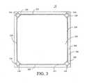
- FIG. 3is a top view of a PBGA package according to one embodiment of the present invention.
- FIG. 4is a perspective view of the PBGA package of FIG. 3 ;
- FIG. 5is a cross-sectional view of the PBGA package of FIG. 4 along line “B-B”;
- FIG. 6is a cross-sectional view illustrating a mold chase for performing a molding process according to an embodiment of the present invention.
- a semiconductor packagecomprises a substrate having upper and lower surface. Conductive traces are formed in the substrate for routing electrical signals, and electrical contacts are on the substrate lower surface. Vias are provided to connect the conductive traces and the electrical contacts.
- a semiconductor dieis attached on the upper surface of the substrate and electrically connected to the conductive traces.
- a solder maskalso is formed over the upper surface of the substrate.
- a mold capthen is formed over the semiconductor die and electrical connections between the die and the conductive traces.
- the mold capincludes a mold body having chamfered corners. A plurality of extensions respectively extend from each of the chamfered corners of the mold body. The extensions preferably do not extend all the way to the substrate edges.
- the plurality of extensionshave a height that is less than a height of the mold body, and a length that is two thirds (2 ⁇ 3) the distance from the clipped corners of the mold body to the corresponding corners of the substrate.
- the plurality of extensionsare shaped as a rectangle with a flat or radius top, and are formed together with the mold body.
- the mold capis provided with extensions extending from the chamfered corners, a greater area of the solder mask that would be otherwise exposed due to the chamfered corners is covered by the extensions, which reduces the risk of cracking of the solder mask and conductive traces.
- the PBGA package 20includes a substrate 200 formed of, for example, a ceramic material, or a plastic material such as epoxy-glass.
- the substrate 200may comprise a plurality of alternating conductive and insulative layers, as is known in the art.
- the substrate 200is covered with a solder mask 202 , and has an upper surface 204 and a lower surface 206 .
- a plurality of conductive traces 208shown formed along the upper surface of the substrate 200 , are electrically connected to a plurality of electrical contacts 210 by way of a plurality of vias 212 (only one is shown), as is known in the art.
- the electrical contacts 210may comprise an array of conductive balls, such as C4 or C5 solder balls, that allow electrical connection between the semiconductor package 20 and external electronic components, such as printed circuit boards (PCBs).
- PCBsprinted circuit boards
- a semiconductor die 214for example, a microcontroller, microprocessor, System on a Chip (SOC), or application specific integrated circuit (ASIC), is attached to the upper surface 204 of the semiconductor substrate 200 with a die attach material 216 , such as epoxy.
- a die attach material 216such as epoxy.
- electrical connection between bond pads (not shown) on the die 214 and the conductive traces 208 in the substrate 200is provided by bond wires 218 .
- bond wires 218it will be understood by those of skill in the art that the present invention is limited to wire bond packages.
- a mold cap 220is formed on the upper surface 204 of the substrate 200 .
- the mold cap 220may be formed on the substrate upper surface 204 by a transfer or injection molding process, which will be discussed in greater detail below.
- the height of the mold cap 220 from the upper surface 204 of the substrate 200is sufficient to fully cover the die 214 and the bond wires 218 .
- the material used to the form mold cap 220is not critical, and commercially available plastic or encapsulant materials may be used as a matter of design choice.
- the mold cap 220has a mold body 222 and a plurality of extensions 224 that extend outwardly from the mold body 220 .
- the mold bodyalso has four sides 226 and four corners 228 .
- each of the four sides 226 of the mold body 222is sloped to facilitate removal of the semiconductor package 200 from a cavity bar (not shown).
- each of the four corners 228 of the mold body 222is clipped or chamfered such that adjacent sides 226 of the mold body 222 do not intersect at right angles.
- the extensions 224have a proximal end that is attached to the mold body 222 and a distal end that is spaced from the mold body 222 .
- the extensions 224extend towards the sides or peripheral edges of the substrate 200 , but preferably do not extend all the way to the peripheral edges of the substrate 200 .
- a height of the extensions 224is less than a height of the mold body 222 .
- the height of the extensions 224is about one-third (1 ⁇ 3) the height of the mold body 222 .
- the extensions 222can be shaped as a rectangle having a radius or flat top, which can be adjusted by adjusting the shape of the cavity bar.
- each extension 224has a length that is about two-thirds (2 ⁇ 3) the distance from the corresponding chamfered corner 228 to the corner of the substrate 200 along the diagonals of the rectangular substrate 200 (see, e.g., line “B-B”.
- the extensions 222preferably cover at least 50% of the exposed solder mask 202 at the corners 228 , which reduces the risk of solder mask 202 cracking.
- Fabrication of semiconductor packages according to the present inventionis performed in a manner similar to conventional transfer or injection molding processes, except that the shape of the cavity bars is designed with extensions at the corners.
- FIG. 6is a cross-sectional view illustrating a mold 300 for performing a molding process according to an embodiment of the present invention, which is generally described with respect to the substrate 200 .
- the mold 300includes an upper mold section 302 and a lower mold section 304 .
- Mold sections 302 and 304in one embodiment are designed as removable cavity bars that fit within a chase (not shown). Platens (not shown) are used to force together the sections 302 , 304 during the molding process, and separate the sections 302 , 304 after the molding process is completed.
- the substrate and die assemblyis placed in the mold 300 and then the assembly is encapsulated.
- the upper mold section 302contains a mold cavity 306 for the insertion of a mold material 308 .
- the lower mold section 304sometimes referred to the “cavity bar”, mates with upper mold section 302 and together they define an opening for the insertion of a transfer ram 310 via the mold cavity 306 into the upper mold section 302 .
- the mold cavity 306is sized and shaped such that its interior volume allows the mold material 308 , when filled, to be formed in a shape in accordance with the present invention, i.e., a mold cap with chamfered corners and extensions at the chamfers.
- the transfer ram 310is pushed into the mold cavity 306 , which causes the mold material 308 to flow into and completely fill the mold cavity 306 .
- the mold material 308is then cured. Curing is performed according to known techniques.
- a plurality of semiconductor packages 20 in accordance with the present inventioncan be manufactured at the same time in a strip or array configuration including multiple substrates 200 , which are later separated or “singulated”, after the molding process. Consequently, packaged electronic devices according to the invention can be produced quickly and at low cost.
Landscapes
- Engineering & Computer Science (AREA)
- Microelectronics & Electronic Packaging (AREA)
- Computer Hardware Design (AREA)
- Power Engineering (AREA)
- Physics & Mathematics (AREA)
- Condensed Matter Physics & Semiconductors (AREA)
- General Physics & Mathematics (AREA)
- Manufacturing & Machinery (AREA)
- Encapsulation Of And Coatings For Semiconductor Or Solid State Devices (AREA)
Abstract
Description
- The present invention relates generally to integrated circuit packaging and, more particularly, to integrated circuit packages formed on laminated substrates, such as BGA (Ball Grid Array) and PBGA (Plastic Ball Grid Array) packages.
- As integrated circuits become more complex, a need has arisen for an integrated circuit package having a greater number of high-density, reliable, external electrical connections. For the integrated circuit package, it is desirable to include one or more conductive layers for signal routing and/or provision of ground and/or power planes. To meet these needs, substrate-based packages such as BGA have been developed.
- In addition, to protect the semiconductor dies and bond wires from damage during handling, physical protection means such as a mold cap is formed on the substrate. A mold cap is formed on the substrate by a transfer or injection molding process. To prevent voids, the mold cap usually has chamfered areas at each of the corners of the substrate. These chamfered corners, unfortunately, leave the corners of the substrate exposed. Thus, the solder mask at the substrate corners is susceptible to cracking during handling. Larger size packages (e.g., 29 mm×29 mm and 31 mm×31 mm) are even more susceptible to solder mask cracking.
FIGS. 1 and 2 show a conventional moldedBGA device 10. Thedevice 10 includes asubstrate 100 having a plurality ofconductive traces 102 and vias104 (only one is shown), asemiconductor die 106 attached to thesubstrate 100 with adie attach material 108, and amold cap 110 formed on thesubstrate 100 to cover and protect the die106 andbond wires 112 that electrically connect the die106 to theconductive traces 102 of thesubstrate 100. Thesemiconductor package 10 also has external electrical connectors in the form ofsolder balls 114. Typically, before forming themold cap 110, asolder mask 116 is formed on thesubstrate 100 to prevent corrosion and oxidation of theconductive traces 112 of thesubstrate 100.- As can be seen in
FIG. 1 , thecorners 118 of themold cap 110 are clipped or chamfered so that thesides 120 of themold cap 110 do not intersect at right angles. This has been found useful to prevent the intrusion of moisture between the junction of themold cap 110 and the upper surface of thesubstrate 100. However, the clippedcorners 118 of themold cap 110 expose thesolder mask 116. During handling, the exposedsolder mask 116 has a high risk of cracking, which in turn makes thetraces 102 susceptible to fracture. - Therefore, it would be desirable to improve the integrated circuit packages to solve the above problem.
- The following detailed description of the preferred embodiments of the present invention will be better understood when read in conjunction with the appended drawings. The present invention is illustrated by way of example, and not limited by the accompanying Figures, in which like references indicate similar elements.
FIG. 1 is a perspective view of a conventional molded BGA package;FIG. 2 is a cross-sectional view of the molded BGA package ofFIG. 1 along line “A-A”;FIG. 3 is a top view of a PBGA package according to one embodiment of the present invention;FIG. 4 is a perspective view of the PBGA package ofFIG. 3 ;FIG. 5 is a cross-sectional view of the PBGA package ofFIG. 4 along line “B-B”; andFIG. 6 is a cross-sectional view illustrating a mold chase for performing a molding process according to an embodiment of the present invention.- The detailed description of the appended drawings is intended as a description of the currently preferred embodiments of the present invention, and is not intended to represent the only form in which the present invention may be practiced. It is to be understood that the same or equivalent functions may be accomplished by different embodiments that are intended to be encompassed within the spirit and scope of the present invention.
- According to one embodiment of the present invention, a semiconductor package comprises a substrate having upper and lower surface. Conductive traces are formed in the substrate for routing electrical signals, and electrical contacts are on the substrate lower surface. Vias are provided to connect the conductive traces and the electrical contacts. A semiconductor die is attached on the upper surface of the substrate and electrically connected to the conductive traces. A solder mask also is formed over the upper surface of the substrate. A mold cap then is formed over the semiconductor die and electrical connections between the die and the conductive traces. The mold cap includes a mold body having chamfered corners. A plurality of extensions respectively extend from each of the chamfered corners of the mold body. The extensions preferably do not extend all the way to the substrate edges.
- In another embodiment of the present invention, the plurality of extensions have a height that is less than a height of the mold body, and a length that is two thirds (⅔) the distance from the clipped corners of the mold body to the corresponding corners of the substrate. In an embodiment of the present invention, the plurality of extensions are shaped as a rectangle with a flat or radius top, and are formed together with the mold body.
- Since the mold cap is provided with extensions extending from the chamfered corners, a greater area of the solder mask that would be otherwise exposed due to the chamfered corners is covered by the extensions, which reduces the risk of cracking of the solder mask and conductive traces.
- The foregoing has outlined rather broadly the features and technical advantages of the present invention in order that the detailed description of the invention that follows may be better understood. Additional features and advantages of the invention will be described hereinafter, which form the subject of the claims of the invention. It should be appreciated by those skilled in the art that the conception and specific embodiments disclosed may be readily used as a basis for modifying or designing other structures or processes for carrying out the same purposes of the present invention. It should also be realized by those skilled in the art that such equivalent constructions do not depart from the spirit and scope of the invention as set forth in the appended claims.
- Referring now to
FIGS. 3-5 , aPBGA package 20 according to one embodiment of the present invention is shown. The PBGApackage 20 includes asubstrate 200 formed of, for example, a ceramic material, or a plastic material such as epoxy-glass. Thesubstrate 200 may comprise a plurality of alternating conductive and insulative layers, as is known in the art. Thesubstrate 200 is covered with asolder mask 202, and has anupper surface 204 and a lower surface206. A plurality ofconductive traces 208, shown formed along the upper surface of thesubstrate 200, are electrically connected to a plurality ofelectrical contacts 210 by way of a plurality of vias212 (only one is shown), as is known in the art. Theelectrical contacts 210 may comprise an array of conductive balls, such as C4 or C5 solder balls, that allow electrical connection between thesemiconductor package 20 and external electronic components, such as printed circuit boards (PCBs). Alternatively, other conventional electrical connectors, such as conductive pins, may be used instead of solder balls. - A
semiconductor die 214, for example, a microcontroller, microprocessor, System on a Chip (SOC), or application specific integrated circuit (ASIC), is attached to theupper surface 204 of thesemiconductor substrate 200 with adie attach material 216, such as epoxy. In the embodiment shown, electrical connection between bond pads (not shown) on thedie 214 and theconductive traces 208 in thesubstrate 200 is provided bybond wires 218. However, it will be understood by those of skill in the art that the present invention is limited to wire bond packages. - To protect the die214 and
bond wires 218, amold cap 220 is formed on theupper surface 204 of thesubstrate 200. Themold cap 220 may be formed on the substrateupper surface 204 by a transfer or injection molding process, which will be discussed in greater detail below. The height of themold cap 220 from theupper surface 204 of thesubstrate 200 is sufficient to fully cover thedie 214 and thebond wires 218. The material used to theform mold cap 220 is not critical, and commercially available plastic or encapsulant materials may be used as a matter of design choice. - The
mold cap 220 has amold body 222 and a plurality ofextensions 224 that extend outwardly from themold body 220. The mold body also has foursides 226 and fourcorners 228. In the embodiment shown, each of the foursides 226 of themold body 222 is sloped to facilitate removal of thesemiconductor package 200 from a cavity bar (not shown). Also, each of the fourcorners 228 of themold body 222 is clipped or chamfered such thatadjacent sides 226 of themold body 222 do not intersect at right angles. - The
extensions 224 have a proximal end that is attached to themold body 222 and a distal end that is spaced from themold body 222. Thus, theextensions 224 extend towards the sides or peripheral edges of thesubstrate 200, but preferably do not extend all the way to the peripheral edges of thesubstrate 200. In one embodiment, a height of theextensions 224 is less than a height of themold body 222. For example, in a preferred embodiment, the height of theextensions 224 is about one-third (⅓) the height of themold body 222. Theextensions 222 can be shaped as a rectangle having a radius or flat top, which can be adjusted by adjusting the shape of the cavity bar. In the embodiment shown, eachextension 224 has a length that is about two-thirds (⅔) the distance from the corresponding chamferedcorner 228 to the corner of thesubstrate 200 along the diagonals of the rectangular substrate200 (see, e.g., line “B-B”. Theextensions 222 preferably cover at least 50% of the exposedsolder mask 202 at thecorners 228, which reduces the risk ofsolder mask 202 cracking. - Fabrication of semiconductor packages according to the present invention is performed in a manner similar to conventional transfer or injection molding processes, except that the shape of the cavity bars is designed with extensions at the corners.
FIG. 6 is a cross-sectional view illustrating a mold300 for performing a molding process according to an embodiment of the present invention, which is generally described with respect to thesubstrate 200. Note that although just one package is shown being formed, it should be understood by those of skill in the art that an array of packages may be formed simultaneously. The mold300 includes anupper mold section 302 and alower mold section 304.Mold sections sections sections - After the
die 214 chip is attached and electrically connected to thesubstrate 200, the substrate and die assembly is placed in the mold300 and then the assembly is encapsulated. - The
upper mold section 302, sometimes referred to as the runner bar, contains amold cavity 306 for the insertion of amold material 308. Thelower mold section 304, sometimes referred to the “cavity bar”, mates withupper mold section 302 and together they define an opening for the insertion of atransfer ram 310 via themold cavity 306 into theupper mold section 302. Themold cavity 306 is sized and shaped such that its interior volume allows themold material 308, when filled, to be formed in a shape in accordance with the present invention, i.e., a mold cap with chamfered corners and extensions at the chamfers. In operation, thetransfer ram 310 is pushed into themold cavity 306, which causes themold material 308 to flow into and completely fill themold cavity 306. Themold material 308 is then cured. Curing is performed according to known techniques. - As mentioned above, a plurality of
semiconductor packages 20 in accordance with the present invention can be manufactured at the same time in a strip or array configuration includingmultiple substrates 200, which are later separated or “singulated”, after the molding process. Consequently, packaged electronic devices according to the invention can be produced quickly and at low cost. - While various embodiments of the present invention have been illustrated and described, it will be clear that the present invention is not limited to these embodiments. Numerous modifications, changes, variations, substitutions, and equivalents will be apparent to those skilled in the art, without departing from the spirit and scope of the present invention, as described in the claims.
Claims (11)
Priority Applications (1)
| Application Number | Priority Date | Filing Date | Title |
|---|---|---|---|
| US13/917,641US9030000B2 (en) | 2013-06-14 | 2013-06-14 | Mold cap for semiconductor device |
Applications Claiming Priority (1)
| Application Number | Priority Date | Filing Date | Title |
|---|---|---|---|
| US13/917,641US9030000B2 (en) | 2013-06-14 | 2013-06-14 | Mold cap for semiconductor device |
Publications (2)
| Publication Number | Publication Date |
|---|---|
| US20140367840A1true US20140367840A1 (en) | 2014-12-18 |
| US9030000B2 US9030000B2 (en) | 2015-05-12 |
Family
ID=52018533
Family Applications (1)
| Application Number | Title | Priority Date | Filing Date |
|---|---|---|---|
| US13/917,641Active2033-10-10US9030000B2 (en) | 2013-06-14 | 2013-06-14 | Mold cap for semiconductor device |
Country Status (1)
| Country | Link |
|---|---|
| US (1) | US9030000B2 (en) |
Cited By (2)
| Publication number | Priority date | Publication date | Assignee | Title |
|---|---|---|---|---|
| US11296002B2 (en)* | 2020-01-03 | 2022-04-05 | Advanced Semiconductor Engineering, Inc. | Semiconductor device package and method for manufacturing the same |
| US11769701B2 (en)* | 2020-02-27 | 2023-09-26 | Infineon Technologies Austria Ag | Protector cap for package with thermal interface material |
Families Citing this family (4)
| Publication number | Priority date | Publication date | Assignee | Title |
|---|---|---|---|---|
| US9662812B2 (en)* | 2012-02-14 | 2017-05-30 | Taiwan Semiconductor Manufacturing Company, Ltd. | Methods for molding integrated circuits |
| US9299692B2 (en)* | 2014-02-07 | 2016-03-29 | Analog Devices Global | Layout of composite circuit elements |
| US10020211B2 (en)* | 2014-06-12 | 2018-07-10 | Taiwan Semiconductor Manufacturing Company, Ltd. | Wafer-level molding chase design |
| US9888561B2 (en) | 2015-07-21 | 2018-02-06 | Apple Inc. | Packaged electrical components with supplemental conductive structures |
Citations (9)
| Publication number | Priority date | Publication date | Assignee | Title |
|---|---|---|---|---|
| US5767446A (en)* | 1995-10-27 | 1998-06-16 | Anam Industrial Co., Ltd. | Printed circuit board having epoxy barrier around a throughout slot and ball grid array semiconductor package |
| US5841192A (en)* | 1994-07-21 | 1998-11-24 | Sgs-Thomson Microelectronics S.A. | Injection molded ball grid array casing |
| US6064117A (en)* | 1997-12-05 | 2000-05-16 | Intel Corporation | Plastic ball grid array assembly |
| US6157086A (en)* | 1997-10-29 | 2000-12-05 | Weber; Patrick O. | Chip package with transfer mold underfill |
| US6177724B1 (en)* | 1999-05-13 | 2001-01-23 | Mitsubishi Denki Kabushiki Kaisha | Semiconductor device |
| US6452268B1 (en)* | 2000-04-26 | 2002-09-17 | Siliconware Precision Industries Co., Ltd. | Integrated circuit package configuration having an encapsulating body with a flanged portion and an encapsulating mold for molding the encapsulating body |
| US6562272B1 (en)* | 2000-12-05 | 2003-05-13 | Cypress Semiconductor Corporation | Apparatus and method for delamination-resistant, array type molding of increased mold cap size laminate packages |
| US7355278B2 (en)* | 2003-03-11 | 2008-04-08 | Hitachi Cable, Ltd. | Mold die for a semiconductor device |
| US20140319682A1 (en)* | 2012-11-07 | 2014-10-30 | Rajen S. Sidhu | Multi-solder techniques and configurations for integrated circuit package assembly |
Family Cites Families (3)
| Publication number | Priority date | Publication date | Assignee | Title |
|---|---|---|---|---|
| US6340792B1 (en) | 1997-04-30 | 2002-01-22 | Nec Corporation | Mold cap for semiconductor device mold package |
| US5886398A (en) | 1997-09-26 | 1999-03-23 | Lsi Logic Corporation | Molded laminate package with integral mold gate |
| US6825067B2 (en) | 2002-12-10 | 2004-11-30 | St Assembly Test Services Pte Ltd | Mold cap anchoring method for molded flex BGA packages |
- 2013
- 2013-06-14USUS13/917,641patent/US9030000B2/enactiveActive
Patent Citations (9)
| Publication number | Priority date | Publication date | Assignee | Title |
|---|---|---|---|---|
| US5841192A (en)* | 1994-07-21 | 1998-11-24 | Sgs-Thomson Microelectronics S.A. | Injection molded ball grid array casing |
| US5767446A (en)* | 1995-10-27 | 1998-06-16 | Anam Industrial Co., Ltd. | Printed circuit board having epoxy barrier around a throughout slot and ball grid array semiconductor package |
| US6157086A (en)* | 1997-10-29 | 2000-12-05 | Weber; Patrick O. | Chip package with transfer mold underfill |
| US6064117A (en)* | 1997-12-05 | 2000-05-16 | Intel Corporation | Plastic ball grid array assembly |
| US6177724B1 (en)* | 1999-05-13 | 2001-01-23 | Mitsubishi Denki Kabushiki Kaisha | Semiconductor device |
| US6452268B1 (en)* | 2000-04-26 | 2002-09-17 | Siliconware Precision Industries Co., Ltd. | Integrated circuit package configuration having an encapsulating body with a flanged portion and an encapsulating mold for molding the encapsulating body |
| US6562272B1 (en)* | 2000-12-05 | 2003-05-13 | Cypress Semiconductor Corporation | Apparatus and method for delamination-resistant, array type molding of increased mold cap size laminate packages |
| US7355278B2 (en)* | 2003-03-11 | 2008-04-08 | Hitachi Cable, Ltd. | Mold die for a semiconductor device |
| US20140319682A1 (en)* | 2012-11-07 | 2014-10-30 | Rajen S. Sidhu | Multi-solder techniques and configurations for integrated circuit package assembly |
Cited By (3)
| Publication number | Priority date | Publication date | Assignee | Title |
|---|---|---|---|---|
| US11296002B2 (en)* | 2020-01-03 | 2022-04-05 | Advanced Semiconductor Engineering, Inc. | Semiconductor device package and method for manufacturing the same |
| US11769701B2 (en)* | 2020-02-27 | 2023-09-26 | Infineon Technologies Austria Ag | Protector cap for package with thermal interface material |
| US12211761B2 (en) | 2020-02-27 | 2025-01-28 | Infineon Technologies Austria Ag | Protector cap for package with thermal interface material |
Also Published As
| Publication number | Publication date |
|---|---|
| US9030000B2 (en) | 2015-05-12 |
Similar Documents
| Publication | Publication Date | Title |
|---|---|---|
| US7245007B1 (en) | Exposed lead interposer leadframe package | |
| US7667338B2 (en) | Package with solder-filled via holes in molding layers | |
| US9030000B2 (en) | Mold cap for semiconductor device | |
| US12354932B2 (en) | SMDs integration on QFN by 3D stacked solution | |
| EP3168864B1 (en) | Packaged devices with multiple planes of embedded electronic devices | |
| JP5707902B2 (en) | Semiconductor device and manufacturing method thereof | |
| US8836115B1 (en) | Stacked inverted flip chip package and fabrication method | |
| US11276628B2 (en) | Semiconductor package with die stacked on surface mounted devices | |
| DE102013114938B4 (en) | Semiconductor component and method for manufacturing a semiconductor component | |
| US20140239497A1 (en) | Packaged semiconductor device | |
| TWI485819B (en) | A package structure and the method to fabricate thereof | |
| US8368192B1 (en) | Multi-chip memory package with a small substrate | |
| US10475730B2 (en) | Preformed lead frame device and lead frame package including the same | |
| US11854947B2 (en) | Integrated circuit chip with a vertical connector | |
| US10008454B1 (en) | Wafer level package with EMI shielding | |
| KR20150014282A (en) | Semiconductor chip package module and manufacturing method | |
| US6921967B2 (en) | Reinforced die pad support structure | |
| US9252114B2 (en) | Semiconductor device grid array package | |
| US9490146B2 (en) | Semiconductor device with encapsulated lead frame contact area and related methods | |
| US9099363B1 (en) | Substrate with corner cut-outs and semiconductor device assembled therewith | |
| US20090096070A1 (en) | Semiconductor package and substrate for the same | |
| CN222394807U (en) | Chip packaging structure and electronic equipment | |
| KR100922372B1 (en) | Semiconductor Package Manufacturing Method | |
| KR200187482Y1 (en) | Ball grid array semiconductor package | |
| KR20100068997A (en) | Universal serial bus memory package |
Legal Events
| Date | Code | Title | Description |
|---|---|---|---|
| AS | Assignment | Owner name:FREESCALE SEMICONDUCTOR, INC., TEXAS Free format text:ASSIGNMENT OF ASSIGNORS INTEREST;ASSIGNORS:EU, POH LENG;LOW, BOON YEW;YOW, KAI YUN;REEL/FRAME:030610/0382 Effective date:20130527 | |
| AS | Assignment | Owner name:CITIBANK, N.A., AS NOTES COLLATERAL AGENT, NEW YOR Free format text:SUPPLEMENT TO IP SECURITY AGREEMENT;ASSIGNOR:FREESCALE SEMICONDUCTOR, INC.;REEL/FRAME:031248/0698 Effective date:20130731 Owner name:CITIBANK, N.A., AS NOTES COLLATERAL AGENT, NEW YOR Free format text:SUPPLEMENT TO IP SECURITY AGREEMENT;ASSIGNOR:FREESCALE SEMICONDUCTOR, INC.;REEL/FRAME:031248/0627 Effective date:20130731 Owner name:CITIBANK, N.A., AS NOTES COLLATERAL AGENT, NEW YOR Free format text:SUPPLEMENT TO IP SECURITY AGREEMENT;ASSIGNOR:FREESCALE SEMICONDUCTOR, INC.;REEL/FRAME:031248/0510 Effective date:20130731 Owner name:CITIBANK, N.A., AS COLLATERAL AGENT, NEW YORK Free format text:SUPPLEMENT TO IP SECURITY AGREEMENT;ASSIGNOR:FREESCALE SEMICONDUCTOR, INC.;REEL/FRAME:031248/0750 Effective date:20130731 | |
| AS | Assignment | Owner name:CITIBANK, N.A., AS NOTES COLLATERAL AGENT, NEW YORK Free format text:SECURITY AGREEMENT;ASSIGNOR:FREESCALE SEMICONDUCTOR, INC.;REEL/FRAME:031591/0266 Effective date:20131101 Owner name:CITIBANK, N.A., AS NOTES COLLATERAL AGENT, NEW YOR Free format text:SECURITY AGREEMENT;ASSIGNOR:FREESCALE SEMICONDUCTOR, INC.;REEL/FRAME:031591/0266 Effective date:20131101 | |
| STCF | Information on status: patent grant | Free format text:PATENTED CASE | |
| AS | Assignment | Owner name:FREESCALE SEMICONDUCTOR, INC., TEXAS Free format text:PATENT RELEASE;ASSIGNOR:CITIBANK, N.A., AS COLLATERAL AGENT;REEL/FRAME:037357/0804 Effective date:20151207 Owner name:FREESCALE SEMICONDUCTOR, INC., TEXAS Free format text:PATENT RELEASE;ASSIGNOR:CITIBANK, N.A., AS COLLATERAL AGENT;REEL/FRAME:037357/0819 Effective date:20151207 Owner name:FREESCALE SEMICONDUCTOR, INC., TEXAS Free format text:PATENT RELEASE;ASSIGNOR:CITIBANK, N.A., AS COLLATERAL AGENT;REEL/FRAME:037357/0844 Effective date:20151207 | |
| AS | Assignment | Owner name:MORGAN STANLEY SENIOR FUNDING, INC., MARYLAND Free format text:ASSIGNMENT AND ASSUMPTION OF SECURITY INTEREST IN PATENTS;ASSIGNOR:CITIBANK, N.A.;REEL/FRAME:037445/0592 Effective date:20151207 | |
| AS | Assignment | Owner name:MORGAN STANLEY SENIOR FUNDING, INC., MARYLAND Free format text:ASSIGNMENT AND ASSUMPTION OF SECURITY INTEREST IN PATENTS;ASSIGNOR:CITIBANK, N.A.;REEL/FRAME:037518/0292 Effective date:20151207 | |
| AS | Assignment | Owner name:MORGAN STANLEY SENIOR FUNDING, INC., MARYLAND Free format text:SUPPLEMENT TO THE SECURITY AGREEMENT;ASSIGNOR:FREESCALE SEMICONDUCTOR, INC.;REEL/FRAME:039138/0001 Effective date:20160525 | |
| AS | Assignment | Owner name:NXP, B.V., F/K/A FREESCALE SEMICONDUCTOR, INC., NETHERLANDS Free format text:RELEASE BY SECURED PARTY;ASSIGNOR:MORGAN STANLEY SENIOR FUNDING, INC.;REEL/FRAME:040925/0001 Effective date:20160912 Owner name:NXP, B.V., F/K/A FREESCALE SEMICONDUCTOR, INC., NE Free format text:RELEASE BY SECURED PARTY;ASSIGNOR:MORGAN STANLEY SENIOR FUNDING, INC.;REEL/FRAME:040925/0001 Effective date:20160912 | |
| AS | Assignment | Owner name:NXP B.V., NETHERLANDS Free format text:RELEASE BY SECURED PARTY;ASSIGNOR:MORGAN STANLEY SENIOR FUNDING, INC.;REEL/FRAME:040928/0001 Effective date:20160622 | |
| AS | Assignment | Owner name:NXP USA, INC., TEXAS Free format text:CHANGE OF NAME;ASSIGNOR:FREESCALE SEMICONDUCTOR, INC.;REEL/FRAME:040632/0001 Effective date:20161107 | |
| AS | Assignment | Owner name:MORGAN STANLEY SENIOR FUNDING, INC., MARYLAND Free format text:CORRECTIVE ASSIGNMENT TO CORRECT THE REMOVE PATENTS 8108266 AND 8062324 AND REPLACE THEM WITH 6108266 AND 8060324 PREVIOUSLY RECORDED ON REEL 037518 FRAME 0292. ASSIGNOR(S) HEREBY CONFIRMS THE ASSIGNMENT AND ASSUMPTION OF SECURITY INTEREST IN PATENTS;ASSIGNOR:CITIBANK, N.A.;REEL/FRAME:041703/0536 Effective date:20151207 | |
| AS | Assignment | Owner name:NXP USA, INC., TEXAS Free format text:CORRECTIVE ASSIGNMENT TO CORRECT THE NATURE OF CONVEYANCE PREVIOUSLY RECORDED AT REEL: 040632 FRAME: 0001. ASSIGNOR(S) HEREBY CONFIRMS THE MERGER AND CHANGE OF NAME;ASSIGNOR:FREESCALE SEMICONDUCTOR INC.;REEL/FRAME:044209/0047 Effective date:20161107 | |
| MAFP | Maintenance fee payment | Free format text:PAYMENT OF MAINTENANCE FEE, 4TH YEAR, LARGE ENTITY (ORIGINAL EVENT CODE: M1551); ENTITY STATUS OF PATENT OWNER: LARGE ENTITY Year of fee payment:4 | |
| AS | Assignment | Owner name:SHENZHEN XINGUODU TECHNOLOGY CO., LTD., CHINA Free format text:CORRECTIVE ASSIGNMENT TO CORRECT THE TO CORRECT THE APPLICATION NO. FROM 13,883,290 TO 13,833,290 PREVIOUSLY RECORDED ON REEL 041703 FRAME 0536. ASSIGNOR(S) HEREBY CONFIRMS THE THE ASSIGNMENT AND ASSUMPTION OF SECURITYINTEREST IN PATENTS.;ASSIGNOR:MORGAN STANLEY SENIOR FUNDING, INC.;REEL/FRAME:048734/0001 Effective date:20190217 | |
| AS | Assignment | Owner name:NXP B.V., NETHERLANDS Free format text:RELEASE BY SECURED PARTY;ASSIGNOR:MORGAN STANLEY SENIOR FUNDING, INC.;REEL/FRAME:050744/0097 Effective date:20190903 | |
| AS | Assignment | Owner name:NXP B.V., NETHERLANDS Free format text:CORRECTIVE ASSIGNMENT TO CORRECT THE REMOVEAPPLICATION 11759915 AND REPLACE IT WITH APPLICATION11759935 PREVIOUSLY RECORDED ON REEL 040928 FRAME 0001. ASSIGNOR(S) HEREBY CONFIRMS THE RELEASE OF SECURITYINTEREST;ASSIGNOR:MORGAN STANLEY SENIOR FUNDING, INC.;REEL/FRAME:052915/0001 Effective date:20160622 | |
| AS | Assignment | Owner name:NXP, B.V. F/K/A FREESCALE SEMICONDUCTOR, INC., NETHERLANDS Free format text:CORRECTIVE ASSIGNMENT TO CORRECT THE REMOVEAPPLICATION 11759915 AND REPLACE IT WITH APPLICATION11759935 PREVIOUSLY RECORDED ON REEL 040925 FRAME 0001. ASSIGNOR(S) HEREBY CONFIRMS THE RELEASE OF SECURITYINTEREST;ASSIGNOR:MORGAN STANLEY SENIOR FUNDING, INC.;REEL/FRAME:052917/0001 Effective date:20160912 | |
| MAFP | Maintenance fee payment | Free format text:PAYMENT OF MAINTENANCE FEE, 8TH YEAR, LARGE ENTITY (ORIGINAL EVENT CODE: M1552); ENTITY STATUS OF PATENT OWNER: LARGE ENTITY Year of fee payment:8 |