US20140354301A1 - Edgeless Single-Layer Touch Sensor - Google Patents
Edgeless Single-Layer Touch SensorDownload PDFInfo
- Publication number
- US20140354301A1 US20140354301A1US13/904,904US201313904904AUS2014354301A1US 20140354301 A1US20140354301 A1US 20140354301A1US 201313904904 AUS201313904904 AUS 201313904904AUS 2014354301 A1US2014354301 A1US 2014354301A1
- Authority
- US
- United States
- Prior art keywords
- electrode
- drive
- sense
- electrodes
- column
- Prior art date
- Legal status (The legal status is an assumption and is not a legal conclusion. Google has not performed a legal analysis and makes no representation as to the accuracy of the status listed.)
- Granted
Links
Images


Classifications
- G—PHYSICS
- G06—COMPUTING OR CALCULATING; COUNTING
- G06F—ELECTRIC DIGITAL DATA PROCESSING
- G06F3/00—Input arrangements for transferring data to be processed into a form capable of being handled by the computer; Output arrangements for transferring data from processing unit to output unit, e.g. interface arrangements
- G06F3/01—Input arrangements or combined input and output arrangements for interaction between user and computer
- G06F3/03—Arrangements for converting the position or the displacement of a member into a coded form
- G06F3/041—Digitisers, e.g. for touch screens or touch pads, characterised by the transducing means
- G06F3/0416—Control or interface arrangements specially adapted for digitisers
- G06F3/04164—Connections between sensors and controllers, e.g. routing lines between electrodes and connection pads
- G—PHYSICS
- G01—MEASURING; TESTING
- G01R—MEASURING ELECTRIC VARIABLES; MEASURING MAGNETIC VARIABLES
- G01R27/00—Arrangements for measuring resistance, reactance, impedance, or electric characteristics derived therefrom
- G01R27/02—Measuring real or complex resistance, reactance, impedance, or other two-pole characteristics derived therefrom, e.g. time constant
- G01R27/26—Measuring inductance or capacitance; Measuring quality factor, e.g. by using the resonance method; Measuring loss factor; Measuring dielectric constants ; Measuring impedance or related variables
- G01R27/2605—Measuring capacitance
- G—PHYSICS
- G06—COMPUTING OR CALCULATING; COUNTING
- G06F—ELECTRIC DIGITAL DATA PROCESSING
- G06F3/00—Input arrangements for transferring data to be processed into a form capable of being handled by the computer; Output arrangements for transferring data from processing unit to output unit, e.g. interface arrangements
- G06F3/01—Input arrangements or combined input and output arrangements for interaction between user and computer
- G06F3/03—Arrangements for converting the position or the displacement of a member into a coded form
- G06F3/041—Digitisers, e.g. for touch screens or touch pads, characterised by the transducing means
- G06F3/044—Digitisers, e.g. for touch screens or touch pads, characterised by the transducing means by capacitive means
- G06F3/0443—Digitisers, e.g. for touch screens or touch pads, characterised by the transducing means by capacitive means using a single layer of sensing electrodes
- G—PHYSICS
- G06—COMPUTING OR CALCULATING; COUNTING
- G06F—ELECTRIC DIGITAL DATA PROCESSING
- G06F3/00—Input arrangements for transferring data to be processed into a form capable of being handled by the computer; Output arrangements for transferring data from processing unit to output unit, e.g. interface arrangements
- G06F3/01—Input arrangements or combined input and output arrangements for interaction between user and computer
- G06F3/03—Arrangements for converting the position or the displacement of a member into a coded form
- G06F3/041—Digitisers, e.g. for touch screens or touch pads, characterised by the transducing means
- G06F3/044—Digitisers, e.g. for touch screens or touch pads, characterised by the transducing means by capacitive means
- G06F3/0446—Digitisers, e.g. for touch screens or touch pads, characterised by the transducing means by capacitive means using a grid-like structure of electrodes in at least two directions, e.g. using row and column electrodes
- G—PHYSICS
- G06—COMPUTING OR CALCULATING; COUNTING
- G06F—ELECTRIC DIGITAL DATA PROCESSING
- G06F3/00—Input arrangements for transferring data to be processed into a form capable of being handled by the computer; Output arrangements for transferring data from processing unit to output unit, e.g. interface arrangements
- G06F3/01—Input arrangements or combined input and output arrangements for interaction between user and computer
- G06F3/03—Arrangements for converting the position or the displacement of a member into a coded form
- G06F3/041—Digitisers, e.g. for touch screens or touch pads, characterised by the transducing means
- G06F3/044—Digitisers, e.g. for touch screens or touch pads, characterised by the transducing means by capacitive means
- G06F3/0448—Details of the electrode shape, e.g. for enhancing the detection of touches, for generating specific electric field shapes, for enhancing display quality
- H—ELECTRICITY
- H03—ELECTRONIC CIRCUITRY
- H03K—PULSE TECHNIQUE
- H03K17/00—Electronic switching or gating, i.e. not by contact-making and –breaking
- H03K17/94—Electronic switching or gating, i.e. not by contact-making and –breaking characterised by the way in which the control signals are generated
- H03K17/96—Touch switches
- H03K17/962—Capacitive touch switches
- G—PHYSICS
- G06—COMPUTING OR CALCULATING; COUNTING
- G06F—ELECTRIC DIGITAL DATA PROCESSING
- G06F2203/00—Indexing scheme relating to G06F3/00 - G06F3/048
- G06F2203/041—Indexing scheme relating to G06F3/041 - G06F3/045
- G06F2203/04101—2.5D-digitiser, i.e. digitiser detecting the X/Y position of the input means, finger or stylus, also when it does not touch, but is proximate to the digitiser's interaction surface and also measures the distance of the input means within a short range in the Z direction, possibly with a separate measurement setup
- H—ELECTRICITY
- H03—ELECTRONIC CIRCUITRY
- H03K—PULSE TECHNIQUE
- H03K17/00—Electronic switching or gating, i.e. not by contact-making and –breaking
- H03K17/94—Electronic switching or gating, i.e. not by contact-making and –breaking characterised by the way in which the control signals are generated
- H03K17/96—Touch switches
- H03K2017/9602—Touch switches characterised by the type or shape of the sensing electrodes
- H—ELECTRICITY
- H03—ELECTRONIC CIRCUITRY
- H03K—PULSE TECHNIQUE
- H03K2217/00—Indexing scheme related to electronic switching or gating, i.e. not by contact-making or -breaking covered by H03K17/00
- H03K2217/94—Indexing scheme related to electronic switching or gating, i.e. not by contact-making or -breaking covered by H03K17/00 characterised by the way in which the control signal is generated
- H03K2217/96—Touch switches
- H03K2217/9607—Capacitive touch switches
- H03K2217/960755—Constructional details of capacitive touch and proximity switches
- H03K2217/960775—Emitter-receiver or "fringe" type detection, i.e. one or more field emitting electrodes and corresponding one or more receiving electrodes
Definitions
- This disclosuregenerally relates to touch sensors.
- An array of conductive drive and sense electrodesmay form a mutual-capacitance touch sensor having one or more capacitive nodes.
- the mutual-capacitance touch sensormay have either a two-layer configuration or single-layer configuration.
- drive and sense electrodesmay be disposed in a pattern on one side of a substrate. In such a configuration, a pair of drive and sense electrodes capacitively coupled to each other across a space or dielectric between electrodes may form a capacitive node.
- an array of vertical and horizontal conductive electrodesmay be disposed in a pattern on one side of the substrate.
- Each of the conductive electrodes in the arraymay form a capacitive node, and, when an object touches or comes within proximity of the electrode, a change in self-capacitance may occur at that capacitive node and a controller may measure the change in capacitance as a change in voltage or a change in the amount of charge needed to raise the voltage to some pre-determined amount.
- a touch sensordetects the presence and location of a touch or the proximity of an object (such as a user's finger or a stylus) within a touch-sensitive area of the touch sensor overlaid, for example, on a display screen.
- the touch sensorenables a user to interact directly with what is displayed on the screen, rather than indirectly with a mouse or touchpad.
- a touch sensormay be attached to or provided as part of a desktop computer, laptop computer, tablet computer, personal digital assistant (PDA), smartphone, satellite navigation device, portable media player, portable game console, kiosk computer, point-of-sale device, or other suitable device.
- a control panel on a household or other appliancemay include a touch sensor.
- touch sensorssuch as resistive touch screens, surface acoustic wave touch screens, capacitive touch screens, infrared touch screens, and optical touch screens.
- reference to a touch sensorencompasses a touch screen, and vice versa, where appropriate.
- a capacitive touch screenmay include an insulator coated with a substantially transparent conductor in a particular pattern.
- FIG. 1illustrates a touch sensor with an example controller, according to example embodiments
- FIG. 2illustrates a pattern for the touch sensor of FIG. 1 , according to example embodiments
- FIG. 3illustrates another orientation for the touch sensor pattern of FIG. 2 , according to example embodiments.
- FIGS. 4A-4Hillustrate another pattern for the touch sensor of FIG. 1 , according to example embodiments.
- FIG. 1illustrates an example touch sensor 10 with an example controller 12 .
- a touch sensormay encompass a touch screen, and vice versa, where appropriate.
- Touch sensor 10 and controller 12detect the presence and location of a touch or the proximity of an object within a touch-sensitive area of touch sensor 10 .
- reference to a touch sensorencompasses both the touch sensor and its controller, where appropriate.
- reference to a controllerencompasses both the controller and its touch sensor, where appropriate.
- Touch sensor 10includes one or more touch-sensitive areas, where appropriate.
- Touch sensor 10includes an array of drive and sense electrodes disposed on a substrate, which in some embodiments is a dielectric material.
- one or more portions of the substrate of touch sensor 10are made of polyethylene terephthalate (PET) or another suitable material.
- PETpolyethylene terephthalate
- the drive electrodes, sense electrodes, and other conductors in touch sensor 10are made of indium tin oxide (ITO), copper or copper-based materials, silver or silver-based materials, carbon-based materials (e.g., graphene plus carbon nanotubes, buds, and wires), conductive polymers, or any other appropriate material, in whole or in part.
- the drive or sense electrodes in touch sensor 10are made of fine lines of metal or other conductive material.
- one or more portions of the conductive materialare copper or copper-based and have a thickness of approximately 5 ⁇ m or less and a width of approximately 10 ⁇ m or less.
- one or more portions of the conductive materialare silver or silver-based and similarly have a thickness of approximately 5 ⁇ m or less and a width of approximately 10 ⁇ m or less.
- This disclosurecontemplates any suitable electrodes made of any suitable material.
- touch sensor 10implements a capacitive form of touch sensing.
- touch sensor 10includes an array of drive and sense electrodes forming an array of capacitive nodes.
- a drive electrode and a sense electrodeform a capacitive node.
- the drive and sense electrodes forming the capacitive nodecome near each other, but do not make electrical contact with each other. Instead, the drive and sense electrodes are capacitively coupled to each other across a gap between them.
- a pulsed or alternating voltage applied to the drive electrodei.e., by controller 12 ) induces a charge on the sense electrode, and the amount of charge induced is susceptible to external influence (such as a touch or the proximity of an object).
- controller 12determines the position of the touch or proximity within the touch-sensitive area(s) of touch sensor 10 .
- one or more drive electrodestogether form a drive line running horizontally or vertically or in any suitable orientation.
- one or more sense electrodestogether form a sense line running horizontally or vertically or in any suitable orientation.
- drive linesrun substantially perpendicular to sense lines.
- reference to a drive lineencompasses one or more drive electrodes making up the drive line, and vice versa, where appropriate.
- reference to a sense lineencompasses one or more sense electrodes making up the sense line, and vice versa, where appropriate.
- touch sensor 10has a single-layer configuration, with drive and sense electrodes disposed in a pattern on one side of a substrate.
- a pair of drive and sense electrodes capacitively coupled to each other across a space between themforms a capacitive node.
- electrodes of only a single typee.g. drive
- this disclosuredescribes particular configurations of particular electrodes forming particular nodes, this disclosure contemplates any suitable configuration of any suitable electrodes forming any suitable nodes.
- this disclosurecontemplates any suitable electrodes disposed on any suitable number of any suitable substrates in any suitable patterns.
- a change in capacitance at a capacitive node of touch sensor 10may indicate a touch or proximity input at the position of the capacitive node.
- Controller 12is operable to detect and process the change in capacitance to determine the presence and location of the touch or proximity input. Certain embodiments if controller 12 communicate information about the touch or proximity input to one or more other components (such one or more central processing units (CPUs) or digital signal processors (DSPs)) of a device that includes touch sensor 10 and controller 12 , which may respond to the touch or proximity input by initiating a function of the device (or an application running on the device) associated with it.
- CPUscentral processing units
- DSPsdigital signal processors
- controller 12is one or more integrated circuits (ICs)—such as for example general-purpose microprocessors, microcontrollers, programmable logic devices or arrays, and application-specific ICs (ASICs).
- controller 12is coupled to a flexible printed circuit (FPC) bonded to the substrate of touch sensor 10 , as described below.
- FPCflexible printed circuit
- controller 12include a processor unit, a drive unit, a sense unit, and a storage unit.
- the drive unitsupplies drive signals to the drive electrodes of touch sensor 10 .
- the sense unitsenses charge at the capacitive nodes of touch sensor 10 and provides measurement signals to the processor unit representing capacitances at the capacitive nodes.
- the processor unitcontrols the supply of drive signals to the drive electrodes by the drive unit and process measurement signals from the sense unit to detect and process the presence and location of a touch or proximity input within the touch-sensitive area(s) of touch sensor 10 .
- the processor unitalso tracks changes in the position of a touch or proximity input within the touch-sensitive area(s) of touch sensor 10 .
- the storage unitwhich includes one or more memory devices, stores programming for execution by the processor unit, including programming for controlling the drive unit to supply drive signals to the drive electrodes, programming for processing measurement signals from the sense unit, and other suitable programming, where appropriate.
- Tracks 14 of conductive material disposed on the substrate of touch sensor 10couple the drive or sense electrodes of touch sensor 10 to connection pads 16 , also disposed on the substrate of touch sensor 10 .
- connection pads 16facilitate coupling of tracks 14 to controller 12 .
- tracks 14extend into or around (e.g. at the edges of) the touch-sensitive area(s) of touch sensor 10 .
- Particular tracks 14provide drive connections for coupling controller 12 to drive electrodes of touch sensor 10 , through which the drive unit of controller 12 supplies drive signals to the drive electrodes.
- Other tracks 14provide sense connections for coupling controller 12 to sense electrodes of touch sensor 10 , through which the sense unit of controller 12 senses charge at the capacitive nodes of touch sensor 10 .
- tracks 14are made of fine lines of metal or other conductive material.
- the conductive material of tracks 14is copper or copper-based and has a width of approximately 100 ⁇ m or less.
- the conductive material of tracks 14is silver or silver-based and has a width of approximately 100 ⁇ m or less.
- tracks 14are made of ITO in whole or in part in addition or as an alternative to fine lines of metal or other conductive material.
- this disclosuredescribes particular tracks made of particular materials with particular widths, this disclosure contemplates any suitable tracks made of any suitable materials with any suitable widths.
- certain embodiments of touch sensor 10include one or more ground lines terminating at a ground connector (similar to a connection pad 16 ) at an edge of the substrate of touch sensor 10 (similar to tracks 14 ).
- connection pads 16are located along one or more edges of the substrate, outside the touch-sensitive area(s) of touch sensor 10 .
- controller 12is on an FPC in certain embodiments.
- connection pads 16are made of the same material as tracks 14 and are bonded to the FPC using an anisotropic conductive film (ACF).
- ACFanisotropic conductive film
- connection 18includes conductive lines on the FPC coupling controller 12 to connection pads 16 , in turn coupling controller 12 to tracks 14 and to the drive or sense electrodes of touch sensor 10 .
- connection pads 160are inserted into an electro-mechanical connector (such as a zero insertion force wire-to-board connector); in this embodiment, connection 180 does not need to include an FPC. This disclosure contemplates any suitable connection 18 between controller 12 and touch sensor 10 .
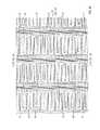
- FIG. 2illustrates an example single-layer touch sensor 10 for use in the example system of FIG. 1 .
- touch sensor 10includes an array of drive electrodes 20 A-E and sense electrodes 22 A-T defining a touch-sensitive area of touch sensor 10 .
- drive electrodes 20 A-E and sense electrodes 22 A-Tare grouped into columns 24 which extend perpendicular to a first direction 31 that extends between a first end 41 and a second end 42 of a substrate.
- Each columnincludes a single drive electrode 20 and one or more sense electrodes 22 .
- Tracks 14couple drive electrodes 20 and sense electrodes 22 to controller 12 and are routed through channels 28 A- 28 D.
- electrodes 20may be sense electrodes and electrodes 22 may be drive electrodes (i.e., the functions of drive electrodes 20 and sense electrodes 22 may be swapped).
- touch sensorsroute tracks such as tracks 14 along the outer edges (e.g., top, bottom, and sides) of the touch sensor. This may be undesirable because it may cause regions along the edges of the touch sensor to be less sensitive to touch.
- Touch sensor 10utilizes columns 24 along the edges of touch sensor 10 (i.e., columns 24 A and 24 E) that are disposed as close to the edge of touch sensor 10 as possible. To do so, touch sensor 10 routes tracks 14 of these edge columns in channels 28 that are on opposite sides of the columns from the edge of the touch sensor.
- tracks 14 of a first column 24 Aare routed in a first channel 28 A that is on the opposite side of column 24 A from first end 41
- tracks 14 of a second column 24 Eare routed in a second channel 28 D that is on the opposite side of column 24 E from second end 42
- the tracks of interior columns 24are then dispersed amongst channels 28 in any appropriate manner or configuration. This allows columns 24 to be pushed out towards the edges of touch sensor 10 and therefore provides improved touch sensitivity along the edges of touch sensor 10 .
- Each column 24 of the arrayincludes a single drive electrode 20 and one or more sense electrodes 22 that are disposed adjacent to the drive electrode 20 of that column.
- column 24 A of the arrayincludes drive electrode 20 A with corresponding sense electrodes 22 A, 22 F, 22 K, and 22 P disposed adjacent to drive electrode 20 A.
- the tracks 14 that couple each sense electrode 22 to controller 12are routed through channels 28 that are substantially parallel to columns 24 of the array.
- tracks 14 A that couple sense electrodes 22 A, 22 F, 22 K, and 22 P to controller 12are routed through channel 28 A.
- the drive electrode 20 of each column 24is capacitively coupled to the one or more adjacent sense electrodes 22 of that column, and a gap 32 separates drive electrode 20 and sense electrodes 22 .
- An electrode(whether a drive electrode 20 or a sense electrode 22 ) is an area of conductive material forming a shape, such as for example a disc, square, rectangle, other suitable shape, or suitable combination of these.
- the conductive material of an electrodee.g., 22 A and 20 C
- the conductive material of an electrodeoccupies approximately 100% of the area of its shape.
- drive and sense electrodes e.g., 22 A and 20 C, along with electrode connectorsare made of indium tin oxide (ITO) and the ITO of the drive and sense electrodes, e.g., 22 A and 20 C, occupies approximately 100% of the area of its shape, where appropriate.
- ITOindium tin oxide
- the conductive material of an electrodeoccupies approximately 50% of the area of its shape.
- an electrode, e.g., 22 A and 20 Cis made of ITO and the ITO of the drive and sense electrodes, e.g., 22 A and 20 C, occupies approximately 50% of the area of its shape in a hatched or other suitable pattern.
- the conductive material of an electrodeoccupies approximately 5% of the area of its shape.
- an electrodee.g., 22 A and 20 C
- an electrode, e.g., 22 A and 20 Cis made of fine lines of metal (such as for example copper, silver, or a copper- or silver-based material) or other conductive material and the fine lines of conductive material occupy approximately 5% of the area of its shape in a hatched or other suitable pattern.
- this disclosuredescribes or illustrates particular electrodes made of particular conductive material forming particular shapes with particular fills having particular patterns, this disclosure contemplates any suitable electrodes made of any suitable conductive material forming any suitable shapes with any suitable fills having any suitable patterns.
- the shapes of the electrodes (or other elements) of a touch sensorconstitute in whole or in part one or more macro-features of certain embodiments of the touch sensor.
- One or more characteristics of the implementation of those shapes(such as, for example, the conductive materials, fills, or patterns within the shapes or the means of electrically isolating or physically separating the shapes from each other) constitute in whole or in part one or more micro-features of certain embodiments of the touch sensor.
- drive electrodes 20 and sense electrodes 22include individual electrode teeth 36 that protrude from main electrode lines 34 and thereby form a caterpillar design.
- electrode teeth 36 of each sense electrode 22 in a particular column 24are adjacent to one or more electrode teeth 36 of a corresponding drive electrode 20 of that column and thereby form capacitive coupling edges that are separated by gap 32 .
- Electrode teeth 36may be interleaved or interdigitated to increase the number of capacitive coupling edges between one or more sense electrodes 22 and a corresponding drive electrode 20 .
- electrode teeth 36 of sense electrodes 22 A, 22 F, 22 K, and 22 Pare interdigitated with electrode teeth 36 of corresponding drive electrode 20 A. Capacitive coupling between sense electrodes and a corresponding drive electrode is determined by dimensions of gap 32 and edges of electrode teeth 36 .
- gap 32is substantially uniform (e.g., gap 32 between drive electrodes 20 and sense electrodes 22 and their corresponding electrode teeth 36 is substantially the same width). In other embodiments, gap 32 may not be uniform.
- certain embodimentsinclude drive electrodes 20 , sense electrodes 22 , and electrode teeth 36 that have substantially similar widths (e.g., the widths of electrode teeth 36 and main electrode lines 34 of drive electrodes 20 and sense electrodes 22 are substantially the same). In other embodiments, drive electrodes 20 , sense electrodes 22 , and electrode teeth 36 do not have substantially similar widths (e.g., the widths of electrode teeth 36 and main electrode lines 34 of drive electrodes 20 and sense electrodes 22 are not substantially the same).
- gap 32is substantially filled with in-fill shapes 46 (illustrated in FIGS. 4A-4H ) that are floating (e.g., not electrically coupled to anything such as drive electrodes 20 or sense electrodes 22 ). In such embodiments, a smaller gap will separate the fill-in shapes 46 and the electrodes.
- the material in gap 32is the same material as drive electrodes 20 and sense electrodes 22 .
- the width of the discrete pieces of material forming the various portions of drive electrodes 20 , sense electrodes 22 , electrode teeth 36 , main electrode lines 34 , etc., and the spacing between those pieces and other portions of touch sensor 10is not uniform. In certain embodiments, the width of those pieces and the spacing between them and other portions of touch sensor 10 is substantially uniform. In embodiments where the width of those pieces and the spacing between them is substantially uniform, visual artifacts are reduced and images viewed through the sensor are affected less than with non-uniform sensors. In such uniform sensor embodiments, the uniformity can be achieved by appropriate design of the various portions of the electrodes of touch sensor 10 and/or by adjusting the spacing between them.
- disconnected pieces of the same material used to form the electrodes of touch sensor 10may be positioned in any open spaces of touch sensor 10 .
- disconnected materialmay be placed in any open space between columns 24 such as between column 24 A and 24 B, and the like.
- open spaces illustrated in FIGS. 3 and 4 A- 4 Hmay also be filled with such disconnected material.
- Such disconnected pieces of material used to fill the open spaces of touch sensor 10are not electrically connected to any tracks 14 and do not function as electrodes.
- main electrode lines 34include one or more electrode teeth 36 that are coupled to and protrude perpendicularly from main electrode line 34 .
- Electrode teeth 36 of a drive electrode 20are generally interdigitated with electrode teeth 36 of one or more sense electrodes 22 .
- electrode teeth 36 of drive electrode 20 Aare interdigitated with electrode teeth 36 of sense electrodes 22 A, 22 F, 22 K, and 22 P (i.e., electrode teeth 36 of drive electrode 20 A are alternating with electrode teeth 36 of sense electrodes 22 A, 22 F, 22 K, and 22 P along a direction that is perpendicular to first direction 31 ).
- gaps 32 and other voids within other areas of the arrayare substantially filled using the conductive material used to fabricate drive electrodes 20 and sense electrodes 22 in such a way to electrically isolate the filled in areas from nearby drive electrodes 20 and sense electrodes 22 or tracks 14 .
- gaps 32 and other voidsare substantially filled using “in-fill” shapes 46 of electrode conductive material isolated from neighboring in-fill shapes by non-conducting gaps.
- the isolated in-fill shapes 46may serve to visually obscure a pattern of drive electrodes 20 and sense electrodes 22 , while having a minimal impact on the fringing fields between adjacent electrodes. Therefore, using in-fill shapes 46 may have electric field distributions substantially similar to electric field distributions without in-fill shapes.
- the in-fillingis formed during manufacture and using the same process steps as drive electrodes 20 and sense electrodes 22 , such that in-fill shapes 46 are formed from the same material and have substantially the same thickness and electrical properties as drive electrodes 20 and sense electrodes 22 .
- in-fill shapes 46reduces a number of areas with optical discontinuities visible when viewing the display.
- in-fill shapesare formed using metal, conductive plastic, ITO, or other form of conductive material, such as fine line metal.
- the material used to fill in a gap 32 and other voidsdepends on the conductive material used to fabricate drive electrodes 20 and sense electrodes 22 .
- certain embodiments of gaps 32 and other voidsare substantially filled in using a series of electrically isolated squares formed during fabrication of drive electrodes 20 and sense electrodes 22 .
- Drive electrodes 20 and sense electrodes 22are coupled to tracks, e.g., tracks 14 A-D, which communicatively couple the electrodes to controller 12 .
- controller 12transmits drive signals to drive electrodes 20 and receives sensing signals from sense electrodes 22 through tracks 14 A-D to determine the position of an object adjacent touch sensor 10 (e.g., a finger or a stylus).
- Tracks 14are routed through channels 28 , which are adjacent to one or more columns 24 .
- the tracks coupled to the electrodes of the outer columnsi.e., columns 24 A and 24 E) are routed through channels 28 that are located on opposite sides of the columns from the edge of touch sensor 10 (e.g., channels 28 A and 28 D).
- Tracks 14 coupled to interior columnsare dispersed amongst channels 28 as discussed in more detail below.
- touch sensor 10includes two columns 24 (i.e., first column 24 A and second column 24 E) that are placed close to or at the edges of touch sensor 20 (e.g., first end 41 and second end 42 , respectively) in order to improve touch sensitivity near the edges of the touch sensor.
- first column 24 Aincludes drive electrode 20 A that is formed from a main electrode line 34 and electrode teeth 36 .
- the main electrode line 34 of drive electrode 20 Ais adjacent to first end 41 and is perpendicular to first direction 31 .
- Electrode teeth 36 of drive electrode 20 Aare coupled to main electrode line 34 of drive electrode 20 A on a side of main electrode line 34 of drive electrode 20 A that is opposite from first end 41 of the substrate (e.g., on the right side of main electrode line 34 of drive electrode 20 A).
- Drive electrode 20 A(and other similarly oriented electrodes such as sense electrode 22 E, 22 J, 22 O, and 22 T) may be hereinafter referred to as “pointing right” or “right-pointing electrodes.”
- second column 24 Eincludes drive electrode 20 E that is formed from a main electrode line 34 and electrode teeth 36 .
- the main electrode line 34 of drive electrode 20 Eis adjacent to second end 42 of the substrate and is perpendicular to first direction 31 .
- Electrode teeth 36 of drive electrode 20 Eare coupled to main electrode line 34 of drive electrode 20 E on a side of main electrode line 34 of drive electrode 20 E that is opposite from second end 41 of the substrate (e.g., on the left side of main electrode line 34 of drive electrode 20 E).
- Drive electrode 20 E(and other similarly oriented electrodes such as sense electrode 22 A. 22 F, 22 K, and 22 P) may be hereinafter referred to as “pointing left” or “left-pointing electrodes.”
- some embodimentsinclude one or more interior columns 24 (e.g., columns 24 B-D).
- Tracks 14 that couple interior columns 24 to controller 12are dispersed amongst channels 28 .
- tracks 14 that couple interior columns 24 A-D of touch sensor 10 in FIG. 2are dispersed amongst channels 28 A-D.
- column 24 Bincludes four sense electrodes: 22 B, 22 G, 22 L, and 22 Q.
- Track 14 coupled to sense electrode 22 Q(the bottom-most sense electrode 22 ) is routed through channel 28 A
- tracks 14 coupled to sense electrodes 22 B, 22 G, and 22 Lare routed through channel 28 B.
- Column 24 Cincludes four sense electrodes: 22 C, 22 H, 22 M, and 22 R.
- Tracks 14 coupled to sense electrodes 22 M and 22 Rare routed through channel 28 B, and tracks 14 coupled to sense electrodes 22 C and 22 H are routed through channel 28 C.
- Column 24 Dincludes four sense electrodes: 22 D, 22 I, 22 N, and 22 S. Tracks 14 coupled to sense electrodes 22 I, 22 N, and 22 S (the three bottom-most sense electrodes 22 ) are routed through channel 28 C, and track 14 coupled to sense electrode 22 D is routed through channel 28 D.
- each interior column 24 of the example touch sensor 10 of FIG. 2includes a drive electrode 20 that has a main electrode line 34 that is not one straight segment as is the case with the outer columns 24 (e.g., columns 24 A and 24 E).
- main electrode lines 34 of the interior columns 24include at least three segments.
- each main electrode line 34 of drive electrodes 20 B-Dinclude two segments that are perpendicular to first direction 31 (e.g., segments 44 A), and one segment that is parallel to first direction 31 (e.g., segment 44 B).
- each interior column 24 in certain embodimentsincludes both left-pointing and right-pointing sense electrodes 22 .
- column 24 Bincludes three left-pointing sense electrodes 22 above segment 44 B (e.g., sense electrodes 22 B, 22 G, and 22 K), and one right-pointing sense electrode 22 below segment 44 B (e.g., sense electrode 22 Q).
- Column 24 Cincludes two left-pointing sense electrodes 22 above segment 44 B (e.g., sense electrodes 22 C and 22 H), and two right-pointing sense electrode 22 below segment 44 B (e.g., sense electrodes 22 M and 22 R).
- Column 24 Dincludes one left-pointing sense electrode 22 above segment 44 B (e.g., sense electrode 22 D), and three right-pointing sense electrodes 22 below segment 44 B (e.g., sense electrodes 22 I, 22 N, and 22 S). While certain arrangements of electrodes 20 and 22 for interior columns 24 are illustrated in FIG. 2 , other embodiments may have other arrangements of these electrodes.
- main electrode line 34may include more than two segments that are perpendicular to first direction 31 and more than one segment that is parallel to first direction 31 in certain embodiments.
- certain embodimentsmay include more than three interior columns (as illustrated in FIGS. 4A-4H ), and the number of sense electrodes 22 above and below segment 44 B may be varied as desired. The disclosure is not limited to the illustrated configuration of electrodes illustrated in FIG. 2 .
- touch sensor 10may include ground lines 30 .
- the touch sensor 10 of FIG. 2includes ground lines 30 located within channels 28 as illustrated.
- ground lines 30may be included around the perimeter of columns 24 as illustrated in FIGS. 4A-4H .
- ground linesmay be tapered (i.e., smaller on one end than the opposite end) as illustrated in FIGS. 4A-4H . While certain ground lines 30 are illustrated in FIGS. 2-4H , this disclosure anticipates any appropriate use and pattern of ground lines 30 .
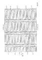
- FIG. 3illustrates another example single-layer touch sensor for use in the example system of FIG. 1 .
- touch sensor 10 in FIG. 3includes an array of drive electrodes 20 A-E and sense electrodes 22 A-T defining a touch-sensitive area of touch sensor 10 .
- drive electrodes 20 A-E and sense electrodes 22 A-Tare grouped into rows 26 which extend perpendicular to first direction 31 that extends between first end 41 and second end 42 of a substrate as illustrated.
- Each row 26includes a single drive electrode 20 and one or more sense electrodes 22 .
- Tracks 14couple drive electrodes 20 and sense electrodes 22 to controller 12 and are routed through channels 28 A- 28 D which run parallel to rows 26 .
- Touch sensor 10utilizes rows 26 along the edges of touch sensor 10 (i.e., rows 26 A and 26 E) that are disposed as close to the top and bottom edges of touch sensor 10 as possible. To do so, touch sensor 10 routes tracks 14 of these edge rows in channels 28 that are on opposite sides of the rows from the edge of the touch sensor. For example, tracks 14 of a first row 26 A are routed in a first channel 28 A that is on the opposite side of row 26 A from first end 41 , and tracks 14 of a second row 26 E are routed in a second channel 28 D that is on the opposite side of row 26 E from second end 42 .
- the tracks of interior rows 26e.g., rows 26 B-D
- Thisallows rows 26 to be pushed out towards the edges of touch sensor 10 and therefore provides improved touch sensitivity along the edges of touch sensor 10 .
- FIGS. 4A-4Hillustrate another example single-layer touch sensor for use in the example system of FIG. 1 .
- the embodiment of touch sensor 10 in FIGS. 4A-4Hincludes an array of drive electrodes 20 and sense electrodes 22 defining a touch-sensitive area of touch sensor 10 .
- drive electrodes 20 and sense electrodes 22are grouped into columns 24 which extend perpendicular to first direction 31 that extends between first end 41 and second end 42 of a substrate as illustrated.
- Each column 24includes a single drive electrode 20 and one or more sense electrodes 22 .
- Tracks 14communicatively couple drive electrodes 20 and sense electrodes 22 to controller 12 and are routed through channels 28 A- 28 D which run parallel to columns 24 .
- each column 24includes nine sense electrodes 22 .
- Other differencesinclude the addition of a ground line 30 surrounding columns 24 , tapered ground lines 30 within channels 28 , and a floating in-fill material between drive electrodes 20 and sense electrodes 22 , as illustrated.
- the touch sensor of FIGS. 4A-4Hincludes interior columns 24 that have an increasing amount of right-facing sense electrodes 22 along first direction 31 . More specifically, column 24 B includes seven left-facing sense electrodes 22 on top of two right-facing sense electrodes 22 , column 24 C includes six left-facing sense electrodes 22 on top of three right-facing sense electrodes 22 , column 24 D includes four left-facing sense electrodes 22 on top of five right-facing sense electrodes 22 , column 24 E includes three left-facing sense electrodes 22 on top of six right-facing sense electrodes 22 , and column 24 F includes two left-facing sense electrodes 22 on top of seven right-facing sense electrodes 22 .
- This configuration of sense electrodes 22 and drive electrodes 20permits tracks 14 coupled to the electrodes of interior columns 24 to be dispersed amongst channels 28 , as previously described.
- sense electrodes 22may share a single track 14 .
- the two bottom-most sense electrodes 22 of columns 24 A and 24 B in FIG. 4Gare coupled to a single track 14 as illustrated.
- sense electrodes 22are each coupled to a separate track 14 (e.g., sense electrodes 22 P and 22 Q are coupled to separate tracks 14 as illustrated in FIG. 2 ).
- electrodes 20are drive electrodes and electrodes 22 are sense electrodes in some embodiments. In other embodiments, electrodes 20 are sense electrodes and electrodes 22 are drive electrodes in some embodiments.
- the disclosureanticipates electrodes 20 and 22 being any suitable combination of drive and sense electrodes.
- electrode teeth 36are illustrated in the figures, the disclosure anticipates any suitable number and density of electrode teeth 36 .
- caterpillar patterns of drive electrodes 20 and sense electrodes 22have been illustrated, these electrodes may be formed of any appropriate pattern or shape.
- a computer-readable storage mediumencompasses one or more non-transitory, tangible computer-readable storage media possessing structure.
- a computer-readable storage mediummay include a semiconductor-based or other integrated circuit (IC) (such, as for example, a field-programmable gate array (FPGA) or an application-specific IC (ASIC)), a hard disk, an HDD, a hybrid hard drive (HHD), an optical disc, an optical disc drive (ODD), a magneto-optical disc, a magneto-optical drive, a floppy disk, a floppy disk drive (FDD), magnetic tape, a holographic storage medium, a solid-state drive (SSD), a RAM-drive, a SECURE DIGITAL card, a SECURE DIGITAL drive, or another suitable computer-readable storage medium or a combination of two or more of these, where appropriate.
- a computer-readable non-transitory storage mediummay be volatile, non-volatile, or a
- references in the appended claims to an apparatus or system or a component of an apparatus or system being adapted to, arranged to, capable of, configured to, enabled to, operable to, or operative to perform a particular functionencompasses that apparatus, system, component, whether or not it or that particular function is activated, turned on, or unlocked, as long as that apparatus, system, or component is so adapted, arranged, capable, configured, enabled, operable, or operative.
Landscapes
- Engineering & Computer Science (AREA)
- General Engineering & Computer Science (AREA)
- Theoretical Computer Science (AREA)
- Physics & Mathematics (AREA)
- General Physics & Mathematics (AREA)
- Human Computer Interaction (AREA)
- Computer Networks & Wireless Communication (AREA)
- Quality & Reliability (AREA)
- Position Input By Displaying (AREA)
Abstract
Description
- This disclosure generally relates to touch sensors.
- An array of conductive drive and sense electrodes may form a mutual-capacitance touch sensor having one or more capacitive nodes. The mutual-capacitance touch sensor may have either a two-layer configuration or single-layer configuration. In a single-layer configuration, drive and sense electrodes may be disposed in a pattern on one side of a substrate. In such a configuration, a pair of drive and sense electrodes capacitively coupled to each other across a space or dielectric between electrodes may form a capacitive node.
- In a single-layer configuration for a self-capacitance implementation, an array of vertical and horizontal conductive electrodes may be disposed in a pattern on one side of the substrate. Each of the conductive electrodes in the array may form a capacitive node, and, when an object touches or comes within proximity of the electrode, a change in self-capacitance may occur at that capacitive node and a controller may measure the change in capacitance as a change in voltage or a change in the amount of charge needed to raise the voltage to some pre-determined amount.
- A touch sensor detects the presence and location of a touch or the proximity of an object (such as a user's finger or a stylus) within a touch-sensitive area of the touch sensor overlaid, for example, on a display screen. In a touch-sensitive-display application, the touch sensor enables a user to interact directly with what is displayed on the screen, rather than indirectly with a mouse or touchpad. A touch sensor may be attached to or provided as part of a desktop computer, laptop computer, tablet computer, personal digital assistant (PDA), smartphone, satellite navigation device, portable media player, portable game console, kiosk computer, point-of-sale device, or other suitable device. A control panel on a household or other appliance may include a touch sensor.
- There are different types of touch sensors, such as (for example) resistive touch screens, surface acoustic wave touch screens, capacitive touch screens, infrared touch screens, and optical touch screens. Herein, reference to a touch sensor encompasses a touch screen, and vice versa, where appropriate. A capacitive touch screen may include an insulator coated with a substantially transparent conductor in a particular pattern. When an object touches or comes within proximity of the surface of the capacitive touch screen, a change in capacitance occurs within the touch screen at the location of the touch or proximity. A controller processes the change in capacitance to determine the touch position(s) on the touch screen.
FIG. 1 illustrates a touch sensor with an example controller, according to example embodiments;FIG. 2 illustrates a pattern for the touch sensor ofFIG. 1 , according to example embodiments;FIG. 3 illustrates another orientation for the touch sensor pattern ofFIG. 2 , according to example embodiments; andFIGS. 4A-4H illustrate another pattern for the touch sensor ofFIG. 1 , according to example embodiments.FIG. 1 illustrates anexample touch sensor 10 with anexample controller 12. Herein, reference to a touch sensor may encompass a touch screen, and vice versa, where appropriate. Touchsensor 10 andcontroller 12 detect the presence and location of a touch or the proximity of an object within a touch-sensitive area oftouch sensor 10. Herein, reference to a touch sensor encompasses both the touch sensor and its controller, where appropriate. Similarly, reference to a controller encompasses both the controller and its touch sensor, where appropriate.Touch sensor 10 includes one or more touch-sensitive areas, where appropriate.Touch sensor 10 includes an array of drive and sense electrodes disposed on a substrate, which in some embodiments is a dielectric material.- In certain embodiments, one or more portions of the substrate of
touch sensor 10 are made of polyethylene terephthalate (PET) or another suitable material. This disclosure contemplates any suitable substrate with any suitable portions made of any suitable material. In particular embodiments, the drive electrodes, sense electrodes, and other conductors intouch sensor 10 are made of indium tin oxide (ITO), copper or copper-based materials, silver or silver-based materials, carbon-based materials (e.g., graphene plus carbon nanotubes, buds, and wires), conductive polymers, or any other appropriate material, in whole or in part. In particular embodiments, the drive or sense electrodes intouch sensor 10 are made of fine lines of metal or other conductive material. As an example and not by way of limitation, one or more portions of the conductive material are copper or copper-based and have a thickness of approximately 5 μm or less and a width of approximately 10 μm or less. As another example, one or more portions of the conductive material are silver or silver-based and similarly have a thickness of approximately 5 μm or less and a width of approximately 10 μm or less. This disclosure contemplates any suitable electrodes made of any suitable material. - In certain embodiments,
touch sensor 10 implements a capacitive form of touch sensing. In a mutual-capacitance implementation,touch sensor 10 includes an array of drive and sense electrodes forming an array of capacitive nodes. In certain embodiments, a drive electrode and a sense electrode form a capacitive node. The drive and sense electrodes forming the capacitive node come near each other, but do not make electrical contact with each other. Instead, the drive and sense electrodes are capacitively coupled to each other across a gap between them. A pulsed or alternating voltage applied to the drive electrode (i.e., by controller12) induces a charge on the sense electrode, and the amount of charge induced is susceptible to external influence (such as a touch or the proximity of an object). When an object touches or comes within proximity of the capacitive node, a change in capacitance occurs at the capacitive node andcontroller 12 measures the change in capacitance. By measuring changes in capacitance throughout the array,controller 12 determines the position of the touch or proximity within the touch-sensitive area(s) oftouch sensor 10. - In particular embodiments, one or more drive electrodes together form a drive line running horizontally or vertically or in any suitable orientation. Similarly, one or more sense electrodes together form a sense line running horizontally or vertically or in any suitable orientation. In particular embodiments, drive lines run substantially perpendicular to sense lines. Herein, reference to a drive line encompasses one or more drive electrodes making up the drive line, and vice versa, where appropriate. Similarly, reference to a sense line encompasses one or more sense electrodes making up the sense line, and vice versa, where appropriate.
- In certain embodiments,
touch sensor 10 has a single-layer configuration, with drive and sense electrodes disposed in a pattern on one side of a substrate. In such a configuration, a pair of drive and sense electrodes capacitively coupled to each other across a space between them forms a capacitive node. In a single-layer configuration for a self-capacitance implementation, electrodes of only a single type (e.g. drive) are disposed in a pattern on one side of the substrate. Although this disclosure describes particular configurations of particular electrodes forming particular nodes, this disclosure contemplates any suitable configuration of any suitable electrodes forming any suitable nodes. Moreover, this disclosure contemplates any suitable electrodes disposed on any suitable number of any suitable substrates in any suitable patterns. - As described above, a change in capacitance at a capacitive node of
touch sensor 10 may indicate a touch or proximity input at the position of the capacitive node.Controller 12 is operable to detect and process the change in capacitance to determine the presence and location of the touch or proximity input. Certain embodiments ifcontroller 12 communicate information about the touch or proximity input to one or more other components (such one or more central processing units (CPUs) or digital signal processors (DSPs)) of a device that includestouch sensor 10 andcontroller 12, which may respond to the touch or proximity input by initiating a function of the device (or an application running on the device) associated with it. Although this disclosure describes a particular controller having particular functionality with respect to a particular device and a particular touch sensor, this disclosure contemplates any suitable controller having any suitable functionality with respect to any suitable device and any suitable touch sensor. - In certain embodiments,
controller 12 is one or more integrated circuits (ICs)—such as for example general-purpose microprocessors, microcontrollers, programmable logic devices or arrays, and application-specific ICs (ASICs). In some embodiments,controller 12 is coupled to a flexible printed circuit (FPC) bonded to the substrate oftouch sensor 10, as described below. Certain embodiments ofcontroller 12 include a processor unit, a drive unit, a sense unit, and a storage unit. The drive unit supplies drive signals to the drive electrodes oftouch sensor 10. The sense unit senses charge at the capacitive nodes oftouch sensor 10 and provides measurement signals to the processor unit representing capacitances at the capacitive nodes. The processor unit controls the supply of drive signals to the drive electrodes by the drive unit and process measurement signals from the sense unit to detect and process the presence and location of a touch or proximity input within the touch-sensitive area(s) oftouch sensor 10. The processor unit also tracks changes in the position of a touch or proximity input within the touch-sensitive area(s) oftouch sensor 10. The storage unit, which includes one or more memory devices, stores programming for execution by the processor unit, including programming for controlling the drive unit to supply drive signals to the drive electrodes, programming for processing measurement signals from the sense unit, and other suitable programming, where appropriate. Although this disclosure describes a particular controller having a particular implementation with particular components, this disclosure contemplates any suitable controller having any suitable implementation with any suitable components. Tracks 14 of conductive material disposed on the substrate oftouch sensor 10 couple the drive or sense electrodes oftouch sensor 10 toconnection pads 16, also disposed on the substrate oftouch sensor 10. As described below,connection pads 16 facilitate coupling oftracks 14 tocontroller 12. In certain embodiments, tracks14 extend into or around (e.g. at the edges of) the touch-sensitive area(s) oftouch sensor 10.Particular tracks 14 provide drive connections for couplingcontroller 12 to drive electrodes oftouch sensor 10, through which the drive unit ofcontroller 12 supplies drive signals to the drive electrodes.Other tracks 14 provide sense connections for couplingcontroller 12 to sense electrodes oftouch sensor 10, through which the sense unit ofcontroller 12 senses charge at the capacitive nodes oftouch sensor 10. In certain embodiments, tracks14 are made of fine lines of metal or other conductive material. As an example and not by way of limitation, the conductive material oftracks 14 is copper or copper-based and has a width of approximately 100 μm or less. As another example, the conductive material oftracks 14 is silver or silver-based and has a width of approximately 100 μm or less. In particular embodiments, tracks14 are made of ITO in whole or in part in addition or as an alternative to fine lines of metal or other conductive material. Although this disclosure describes particular tracks made of particular materials with particular widths, this disclosure contemplates any suitable tracks made of any suitable materials with any suitable widths. In addition totracks 14, certain embodiments oftouch sensor 10 include one or more ground lines terminating at a ground connector (similar to a connection pad16) at an edge of the substrate of touch sensor10 (similar to tracks14).- In certain embodiments,
connection pads 16 are located along one or more edges of the substrate, outside the touch-sensitive area(s) oftouch sensor 10. As described above,controller 12 is on an FPC in certain embodiments. In some embodiments,connection pads 16 are made of the same material astracks 14 and are bonded to the FPC using an anisotropic conductive film (ACF). In certain embodiments,connection 18 includes conductive lines on theFPC coupling controller 12 toconnection pads 16, inturn coupling controller 12 totracks 14 and to the drive or sense electrodes oftouch sensor 10. In another embodiment, connection pads160 are inserted into an electro-mechanical connector (such as a zero insertion force wire-to-board connector); in this embodiment, connection180 does not need to include an FPC. This disclosure contemplates anysuitable connection 18 betweencontroller 12 andtouch sensor 10. FIG. 2 illustrates an example single-layer touch sensor 10 for use in the example system ofFIG. 1 . In the example ofFIG. 2 ,touch sensor 10 includes an array of drive electrodes20A-E andsense electrodes 22A-T defining a touch-sensitive area oftouch sensor 10. In this embodiment, drive electrodes20A-E andsense electrodes 22A-T are grouped into columns24 which extend perpendicular to afirst direction 31 that extends between afirst end 41 and asecond end 42 of a substrate. Each column includes asingle drive electrode 20 and one ormore sense electrodes 22.Tracks 14couple drive electrodes 20 andsense electrodes 22 tocontroller 12 and are routed throughchannels 28A-28D. While a particular number of columns24,drive electrodes 20,sense electrodes 22, and channels28 are illustrated inFIG. 2 , other embodiments may have any appropriate number of these elements. Furthermore, in some embodiments,electrodes 20 may be sense electrodes andelectrodes 22 may be drive electrodes (i.e., the functions ofdrive electrodes 20 andsense electrodes 22 may be swapped).- In general, the example embodiment of
FIG. 2 provides an edgeless single-layer touch sensor that offers many advantages over typical touch sensors. Typically, touch sensors route tracks such astracks 14 along the outer edges (e.g., top, bottom, and sides) of the touch sensor. This may be undesirable because it may cause regions along the edges of the touch sensor to be less sensitive to touch.Touch sensor 10, however, utilizes columns24 along the edges of touch sensor10 (i.e.,columns touch sensor 10 as possible. To do so,touch sensor 10 routes tracks14 of these edge columns in channels28 that are on opposite sides of the columns from the edge of the touch sensor. For example, tracks14 of afirst column 24A are routed in afirst channel 28A that is on the opposite side ofcolumn 24A fromfirst end 41, and tracks14 of asecond column 24E are routed in a second channel28D that is on the opposite side ofcolumn 24E fromsecond end 42. The tracks of interior columns24 (e.g.,columns 24B-D) are then dispersed amongst channels28 in any appropriate manner or configuration. This allows columns24 to be pushed out towards the edges oftouch sensor 10 and therefore provides improved touch sensitivity along the edges oftouch sensor 10. - Each column24 of the array includes a
single drive electrode 20 and one ormore sense electrodes 22 that are disposed adjacent to thedrive electrode 20 of that column. As an example and not by way of limitation,column 24A of the array includes drive electrode20A withcorresponding sense electrodes tracks 14 that couple eachsense electrode 22 tocontroller 12 are routed through channels28 that are substantially parallel to columns24 of the array. As an example and not by way of limitation, tracks14A thatcouple sense electrodes controller 12 are routed throughchannel 28A. Thedrive electrode 20 of each column24 is capacitively coupled to the one or moreadjacent sense electrodes 22 of that column, and agap 32 separates driveelectrode 20 andsense electrodes 22. - An electrode (whether a
drive electrode 20 or a sense electrode22) is an area of conductive material forming a shape, such as for example a disc, square, rectangle, other suitable shape, or suitable combination of these. In particular embodiments, the conductive material of an electrode, e.g.,22A and20C, occupies approximately 100% of the area of its shape. As an example and not by way of limitation, drive and sense electrodes e.g.,22A and20C, along with electrode connectors, are made of indium tin oxide (ITO) and the ITO of the drive and sense electrodes, e.g.,22A and20C, occupies approximately 100% of the area of its shape, where appropriate. In particular embodiments, the conductive material of an electrode, e.g.,22A and20C, occupies approximately 50% of the area of its shape. As an example and not by way of limitation, an electrode, e.g.,22A and20C, is made of ITO and the ITO of the drive and sense electrodes, e.g.,22A and20C, occupies approximately 50% of the area of its shape in a hatched or other suitable pattern. - In particular embodiments, the conductive material of an electrode, e.g.,22A and20C, occupies approximately 5% of the area of its shape. As an example and not by way of limitation, an electrode, e.g.,22A and20C, is made of fine lines of metal (such as for example copper, silver, or a copper- or silver-based material) or other conductive material and the fine lines of conductive material occupy approximately 5% of the area of its shape in a hatched or other suitable pattern. Although this disclosure describes or illustrates particular electrodes made of particular conductive material forming particular shapes with particular fills having particular patterns, this disclosure contemplates any suitable electrodes made of any suitable conductive material forming any suitable shapes with any suitable fills having any suitable patterns. Where appropriate, the shapes of the electrodes (or other elements) of a touch sensor constitute in whole or in part one or more macro-features of certain embodiments of the touch sensor. One or more characteristics of the implementation of those shapes (such as, for example, the conductive materials, fills, or patterns within the shapes or the means of electrically isolating or physically separating the shapes from each other) constitute in whole or in part one or more micro-features of certain embodiments of the touch sensor.
- In particular embodiments, drive
electrodes 20 andsense electrodes 22 includeindividual electrode teeth 36 that protrude frommain electrode lines 34 and thereby form a caterpillar design. In certain embodiments,electrode teeth 36 of eachsense electrode 22 in a particular column24 are adjacent to one ormore electrode teeth 36 of acorresponding drive electrode 20 of that column and thereby form capacitive coupling edges that are separated bygap 32.Electrode teeth 36 may be interleaved or interdigitated to increase the number of capacitive coupling edges between one ormore sense electrodes 22 and acorresponding drive electrode 20. As an example and not by way of limitation,electrode teeth 36 ofsense electrodes electrode teeth 36 of corresponding drive electrode20A. Capacitive coupling between sense electrodes and a corresponding drive electrode is determined by dimensions ofgap 32 and edges ofelectrode teeth 36. - In some embodiments,
gap 32 is substantially uniform (e.g.,gap 32 betweendrive electrodes 20 andsense electrodes 22 and theircorresponding electrode teeth 36 is substantially the same width). In other embodiments,gap 32 may not be uniform. In addition, certain embodiments includedrive electrodes 20,sense electrodes 22, andelectrode teeth 36 that have substantially similar widths (e.g., the widths ofelectrode teeth 36 andmain electrode lines 34 ofdrive electrodes 20 andsense electrodes 22 are substantially the same). In other embodiments, driveelectrodes 20,sense electrodes 22, andelectrode teeth 36 do not have substantially similar widths (e.g., the widths ofelectrode teeth 36 andmain electrode lines 34 ofdrive electrodes 20 andsense electrodes 22 are not substantially the same). In some embodiments,gap 32 is substantially filled with in-fill shapes46 (illustrated inFIGS. 4A-4H ) that are floating (e.g., not electrically coupled to anything such asdrive electrodes 20 or sense electrodes22). In such embodiments, a smaller gap will separate the fill-inshapes 46 and the electrodes. In certain embodiments, the material ingap 32 is the same material asdrive electrodes 20 andsense electrodes 22. Although this disclosure describes and illustrates a particular arrangement of electrodes fortouch sensor 10, this disclosure contemplates any suitable arrangement of electrodes fortouch sensor 10. - In the illustrated embodiment of
FIG. 2 , the width of the discrete pieces of material forming the various portions ofdrive electrodes 20,sense electrodes 22,electrode teeth 36,main electrode lines 34, etc., and the spacing between those pieces and other portions oftouch sensor 10, is not uniform. In certain embodiments, the width of those pieces and the spacing between them and other portions oftouch sensor 10 is substantially uniform. In embodiments where the width of those pieces and the spacing between them is substantially uniform, visual artifacts are reduced and images viewed through the sensor are affected less than with non-uniform sensors. In such uniform sensor embodiments, the uniformity can be achieved by appropriate design of the various portions of the electrodes oftouch sensor 10 and/or by adjusting the spacing between them. As just one example, disconnected pieces of the same material used to form the electrodes oftouch sensor 10 may be positioned in any open spaces oftouch sensor 10. For example, disconnected material may be placed in any open space between columns24 such as betweencolumn touch sensor 10 are not electrically connected to anytracks 14 and do not function as electrodes. - In certain embodiments,
main electrode lines 34 include one ormore electrode teeth 36 that are coupled to and protrude perpendicularly frommain electrode line 34.Electrode teeth 36 of adrive electrode 20 are generally interdigitated withelectrode teeth 36 of one ormore sense electrodes 22. For example,electrode teeth 36 of drive electrode20A are interdigitated withelectrode teeth 36 ofsense electrodes electrode teeth 36 of drive electrode20A are alternating withelectrode teeth 36 ofsense electrodes - Optical properties of
gap 32 as well as voids within other areas of the array with large dimensions relative to feature sizes ofdrive electrodes 20 may have different optical properties than the optical properties of the electrodes (eithersense electrodes 22 or drive electrodes20). Optical discontinuities may occur when viewing a display underneathtouch sensor 10 due to these differences in optical properties. In certain embodiments,gaps 32 and other voids within other areas of the array are substantially filled using the conductive material used to fabricatedrive electrodes 20 andsense electrodes 22 in such a way to electrically isolate the filled in areas fromnearby drive electrodes 20 andsense electrodes 22 or tracks14. In particular embodiments,gaps 32 and other voids are substantially filled using “in-fill”shapes 46 of electrode conductive material isolated from neighboring in-fill shapes by non-conducting gaps. The isolated in-fill shapes 46 may serve to visually obscure a pattern ofdrive electrodes 20 andsense electrodes 22, while having a minimal impact on the fringing fields between adjacent electrodes. Therefore, using in-fill shapes 46 may have electric field distributions substantially similar to electric field distributions without in-fill shapes. In certain embodiments, the in-filling is formed during manufacture and using the same process steps asdrive electrodes 20 andsense electrodes 22, such that in-fill shapes 46 are formed from the same material and have substantially the same thickness and electrical properties asdrive electrodes 20 andsense electrodes 22. - Filling in
gap 32 and other voids using in-fill shapes46 reduces a number of areas with optical discontinuities visible when viewing the display. In particular embodiments, in-fill shapes are formed using metal, conductive plastic, ITO, or other form of conductive material, such as fine line metal. In certain embodiments, the material used to fill in agap 32 and other voids depends on the conductive material used to fabricatedrive electrodes 20 andsense electrodes 22. As an example and not by way of limitation, certain embodiments ofgaps 32 and other voids are substantially filled in using a series of electrically isolated squares formed during fabrication ofdrive electrodes 20 andsense electrodes 22. Although this disclosure describes or illustrates particular in-fill shapes 46 having particular patterns, this disclosure contemplates any suitable in-fill shapes having any suitable patterns. - Drive
electrodes 20 andsense electrodes 22 are coupled to tracks, e.g., tracks14A-D, which communicatively couple the electrodes tocontroller 12. As described above,controller 12 transmits drive signals to driveelectrodes 20 and receives sensing signals fromsense electrodes 22 throughtracks 14A-D to determine the position of an object adjacent touch sensor10 (e.g., a finger or a stylus).Tracks 14 are routed through channels28, which are adjacent to one or more columns24. The tracks coupled to the electrodes of the outer columns (i.e.,columns channels 28A and28D).Tracks 14 coupled to interior columns (e.g.,columns 24B-D) are dispersed amongst channels28 as discussed in more detail below. - As discussed above,
touch sensor 10 includes two columns24 (i.e.,first column 24A andsecond column 24E) that are placed close to or at the edges of touch sensor20 (e.g.,first end 41 andsecond end 42, respectively) in order to improve touch sensitivity near the edges of the touch sensor. In some embodiments,first column 24A includes drive electrode20A that is formed from amain electrode line 34 andelectrode teeth 36. Themain electrode line 34 of drive electrode20A is adjacent tofirst end 41 and is perpendicular tofirst direction 31.Electrode teeth 36 of drive electrode20A are coupled tomain electrode line 34 of drive electrode20A on a side ofmain electrode line 34 of drive electrode20A that is opposite fromfirst end 41 of the substrate (e.g., on the right side ofmain electrode line 34 of drive electrode20A). Drive electrode20A (and other similarly oriented electrodes such assense electrode second column 24E includesdrive electrode 20E that is formed from amain electrode line 34 andelectrode teeth 36. Themain electrode line 34 ofdrive electrode 20E is adjacent tosecond end 42 of the substrate and is perpendicular tofirst direction 31.Electrode teeth 36 ofdrive electrode 20E are coupled tomain electrode line 34 ofdrive electrode 20E on a side ofmain electrode line 34 ofdrive electrode 20E that is opposite fromsecond end 41 of the substrate (e.g., on the left side ofmain electrode line 34 ofdrive electrode 20E).Drive electrode 20E (and other similarly oriented electrodes such assense electrode 22A.22F,22K, and22P) may be hereinafter referred to as “pointing left” or “left-pointing electrodes.” - As discussed above, some embodiments include one or more interior columns24 (e.g.,
columns 24B-D).Tracks 14 that couple interior columns24 tocontroller 12 are dispersed amongst channels28. For example, tracks14 that coupleinterior columns 24A-D oftouch sensor 10 inFIG. 2 are dispersed amongstchannels 28A-D. In particular,column 24B includes four sense electrodes:22B,22G,22L, and22Q.Track 14 coupled to sense electrode22Q (the bottom-most sense electrode22) is routed throughchannel 28A, and tracks14 coupled to senseelectrodes 22B,22G, and22L are routed throughchannel 28B. Column24C includes four sense electrodes:22C,22H,22M, and22R.Tracks 14 coupled tosense electrodes channel 28B, and tracks14 coupled tosense electrodes 22C and22H are routed through channel28C.Column 24D includes four sense electrodes:22D,22I,22N, and22S.Tracks 14 coupled tosense electrodes 22I,22N, and22S (the three bottom-most sense electrodes22) are routed through channel28C, and track14 coupled to sense electrode22D is routed through channel28D. - In order to accommodate the routing of
tracks 14 through the various channels28 as described above, certain embodiments have different arrangements of electrodes within interior columns24. For example, each interior column24 of theexample touch sensor 10 ofFIG. 2 includes adrive electrode 20 that has amain electrode line 34 that is not one straight segment as is the case with the outer columns24 (e.g.,columns main electrode lines 34 of the interior columns24 include at least three segments. For example, eachmain electrode line 34 ofdrive electrodes 20B-D include two segments that are perpendicular to first direction31 (e.g., segments44A), and one segment that is parallel to first direction31 (e.g., segment44B). In addition, each interior column24 in certain embodiments includes both left-pointing and right-pointing sense electrodes 22. For example,column 24B includes three left-pointingsense electrodes 22 above segment44B (e.g.,sense electrodes 22B,22G, and22K), and one right-pointing sense electrode 22 below segment44B (e.g., sense electrode22Q). Column24C includes two left-pointingsense electrodes 22 above segment44B (e.g.,sense electrodes 22C and22H), and two right-pointing sense electrode 22 below segment44B (e.g.,sense electrodes Column 24D includes one left-pointingsense electrode 22 above segment44B (e.g., sense electrode22D), and three right-pointing sense electrodes 22 below segment44B (e.g.,sense electrodes 22I,22N, and22S). While certain arrangements ofelectrodes FIG. 2 , other embodiments may have other arrangements of these electrodes. For example,main electrode line 34 may include more than two segments that are perpendicular tofirst direction 31 and more than one segment that is parallel tofirst direction 31 in certain embodiments. As another example, certain embodiments may include more than three interior columns (as illustrated inFIGS. 4A-4H ), and the number ofsense electrodes 22 above and below segment44B may be varied as desired. The disclosure is not limited to the illustrated configuration of electrodes illustrated inFIG. 2 . - In certain embodiments,
touch sensor 10 may include ground lines30. For example, thetouch sensor 10 ofFIG. 2 includesground lines 30 located within channels28 as illustrated. In other embodiments,ground lines 30 may be included around the perimeter of columns24 as illustrated inFIGS. 4A-4H . In some embodiments, ground lines may be tapered (i.e., smaller on one end than the opposite end) as illustrated inFIGS. 4A-4H . Whilecertain ground lines 30 are illustrated inFIGS. 2-4H , this disclosure anticipates any appropriate use and pattern of ground lines30. FIG. 3 illustrates another example single-layer touch sensor for use in the example system ofFIG. 1 . Similar to the example ofFIG. 2 , the embodiment oftouch sensor 10 inFIG. 3 includes an array of drive electrodes20A-E andsense electrodes 22A-T defining a touch-sensitive area oftouch sensor 10. In this embodiment, however, drive electrodes20A-E andsense electrodes 22A-T are grouped into rows26 which extend perpendicular tofirst direction 31 that extends betweenfirst end 41 andsecond end 42 of a substrate as illustrated. Each row26 includes asingle drive electrode 20 and one ormore sense electrodes 22.Tracks 14couple drive electrodes 20 andsense electrodes 22 tocontroller 12 and are routed throughchannels 28A-28D which run parallel to rows26.- In general, the example embodiment of
FIG. 3 also provides an edgeless single-layer touch sensor that offers many advantages over typical touch sensors.Touch sensor 10 utilizes rows26 along the edges of touch sensor10 (i.e.,rows touch sensor 10 as possible. To do so,touch sensor 10 routes tracks14 of these edge rows in channels28 that are on opposite sides of the rows from the edge of the touch sensor. For example, tracks14 of afirst row 26A are routed in afirst channel 28A that is on the opposite side ofrow 26A fromfirst end 41, and tracks14 of asecond row 26E are routed in a second channel28D that is on the opposite side ofrow 26E fromsecond end 42. The tracks of interior rows26 (e.g.,rows 26B-D) are then dispersed amongst channels28. This allows rows26 to be pushed out towards the edges oftouch sensor 10 and therefore provides improved touch sensitivity along the edges oftouch sensor 10. FIGS. 4A-4H illustrate another example single-layer touch sensor for use in the example system ofFIG. 1 . Similar to the example ofFIG. 2 , the embodiment oftouch sensor 10 inFIGS. 4A-4H includes an array ofdrive electrodes 20 andsense electrodes 22 defining a touch-sensitive area oftouch sensor 10. Like the embodiment ofFIG. 2 , driveelectrodes 20 andsense electrodes 22 are grouped into columns24 which extend perpendicular tofirst direction 31 that extends betweenfirst end 41 andsecond end 42 of a substrate as illustrated. Each column24 includes asingle drive electrode 20 and one ormore sense electrodes 22.Tracks 14 communicativelycouple drive electrodes 20 andsense electrodes 22 tocontroller 12 and are routed throughchannels 28A-28D which run parallel to columns24. In this embodiment however, a total of seven columns24 and six channels28 are provided. In addition, each column24 includes ninesense electrodes 22. Other differences include the addition of aground line 30 surrounding columns24, taperedground lines 30 within channels28, and a floating in-fill material betweendrive electrodes 20 andsense electrodes 22, as illustrated.- Similar to the example embodiment of
FIG. 2 , the touch sensor ofFIGS. 4A-4H includes interior columns24 that have an increasing amount of right-facingsense electrodes 22 alongfirst direction 31. More specifically,column 24B includes seven left-facingsense electrodes 22 on top of two right-facingsense electrodes 22, column24C includes six left-facingsense electrodes 22 on top of three right-facingsense electrodes 22,column 24D includes four left-facingsense electrodes 22 on top of five right-facingsense electrodes 22,column 24E includes three left-facingsense electrodes 22 on top of six right-facingsense electrodes 22, andcolumn 24F includes two left-facingsense electrodes 22 on top of seven right-facingsense electrodes 22. This configuration ofsense electrodes 22 and driveelectrodes 20 permits tracks14 coupled to the electrodes of interior columns24 to be dispersed amongst channels28, as previously described. - In some embodiments,
sense electrodes 22 may share asingle track 14. For example, the twobottom-most sense electrodes 22 ofcolumns FIG. 4G are coupled to asingle track 14 as illustrated. In other embodiments,sense electrodes 22 are each coupled to a separate track14 (e.g.,sense electrodes 22P and22Q are coupled toseparate tracks 14 as illustrated inFIG. 2 ). - As described in detail above,
electrodes 20 are drive electrodes andelectrodes 22 are sense electrodes in some embodiments. In other embodiments,electrodes 20 are sense electrodes andelectrodes 22 are drive electrodes in some embodiments. The disclosure anticipateselectrodes electrode teeth 36 are illustrated in the figures, the disclosure anticipates any suitable number and density ofelectrode teeth 36. Furthermore, while particular caterpillar patterns ofdrive electrodes 20 andsense electrodes 22 have been illustrated, these electrodes may be formed of any appropriate pattern or shape. - Herein, reference to a computer-readable storage medium encompasses one or more non-transitory, tangible computer-readable storage media possessing structure. As an example and not by way of limitation, a computer-readable storage medium may include a semiconductor-based or other integrated circuit (IC) (such, as for example, a field-programmable gate array (FPGA) or an application-specific IC (ASIC)), a hard disk, an HDD, a hybrid hard drive (HHD), an optical disc, an optical disc drive (ODD), a magneto-optical disc, a magneto-optical drive, a floppy disk, a floppy disk drive (FDD), magnetic tape, a holographic storage medium, a solid-state drive (SSD), a RAM-drive, a SECURE DIGITAL card, a SECURE DIGITAL drive, or another suitable computer-readable storage medium or a combination of two or more of these, where appropriate. A computer-readable non-transitory storage medium may be volatile, non-volatile, or a combination of volatile and non-volatile, where appropriate.
- Herein, “or” is inclusive and not exclusive, unless expressly indicated otherwise or indicated otherwise by context. Therefore, herein, “A or B” means “A, B, or both,” unless expressly indicated otherwise or indicated otherwise by context. Moreover, “and” is both joint and several, unless expressly indicated otherwise or indicated otherwise by context. Therefore, herein, “A and B” means “A and B, jointly or severally,” unless expressly indicated otherwise or indicated otherwise by context.
- This disclosure encompasses all changes, substitutions, variations, alterations, and modifications to the example embodiments herein that a person having ordinary skill in the art would comprehend. Similarly, where appropriate, the appended claims encompass all changes, substitutions, variations, alterations, and modifications to the example embodiments herein that a person having ordinary skill in the art would comprehend. Moreover, reference in the appended claims to an apparatus or system or a component of an apparatus or system being adapted to, arranged to, capable of, configured to, enabled to, operable to, or operative to perform a particular function encompasses that apparatus, system, component, whether or not it or that particular function is activated, turned on, or unlocked, as long as that apparatus, system, or component is so adapted, arranged, capable, configured, enabled, operable, or operative.
Claims (20)
Priority Applications (6)
| Application Number | Priority Date | Filing Date | Title |
|---|---|---|---|
| US13/904,904US9557361B2 (en) | 2013-05-29 | 2013-05-29 | Edgeless single-layer touch sensor |
| CN201410227910.3ACN104216582B (en) | 2013-05-29 | 2014-05-27 | Non-flanged single-layer touch sensor |
| DE102014210210.3ADE102014210210A1 (en) | 2013-05-29 | 2014-05-28 | BORDER SINGLE-LAYER TREATMENT SENSOR |
| TW103118873ATWI631489B (en) | 2013-05-29 | 2014-05-29 | Edgeless single-layer touch sensor |
| US15/419,737US10429987B2 (en) | 2013-05-29 | 2017-01-30 | Edgeless single-layer touch sensor |
| US16/507,412US20200012376A1 (en) | 2013-05-29 | 2019-07-10 | Edgeless Single-Layer Touch Sensor |
Applications Claiming Priority (1)
| Application Number | Priority Date | Filing Date | Title |
|---|---|---|---|
| US13/904,904US9557361B2 (en) | 2013-05-29 | 2013-05-29 | Edgeless single-layer touch sensor |
Related Child Applications (1)
| Application Number | Title | Priority Date | Filing Date |
|---|---|---|---|
| US15/419,737ContinuationUS10429987B2 (en) | 2013-05-29 | 2017-01-30 | Edgeless single-layer touch sensor |
Publications (2)
| Publication Number | Publication Date |
|---|---|
| US20140354301A1true US20140354301A1 (en) | 2014-12-04 |
| US9557361B2 US9557361B2 (en) | 2017-01-31 |
Family
ID=51899670
Family Applications (3)
| Application Number | Title | Priority Date | Filing Date |
|---|---|---|---|
| US13/904,904Expired - Fee RelatedUS9557361B2 (en) | 2013-05-29 | 2013-05-29 | Edgeless single-layer touch sensor |
| US15/419,737Expired - Fee RelatedUS10429987B2 (en) | 2013-05-29 | 2017-01-30 | Edgeless single-layer touch sensor |
| US16/507,412AbandonedUS20200012376A1 (en) | 2013-05-29 | 2019-07-10 | Edgeless Single-Layer Touch Sensor |
Family Applications After (2)
| Application Number | Title | Priority Date | Filing Date |
|---|---|---|---|
| US15/419,737Expired - Fee RelatedUS10429987B2 (en) | 2013-05-29 | 2017-01-30 | Edgeless single-layer touch sensor |
| US16/507,412AbandonedUS20200012376A1 (en) | 2013-05-29 | 2019-07-10 | Edgeless Single-Layer Touch Sensor |
Country Status (4)
| Country | Link |
|---|---|
| US (3) | US9557361B2 (en) |
| CN (1) | CN104216582B (en) |
| DE (1) | DE102014210210A1 (en) |
| TW (1) | TWI631489B (en) |
Cited By (29)
| Publication number | Priority date | Publication date | Assignee | Title |
|---|---|---|---|---|
| US20150193047A1 (en)* | 2013-09-10 | 2015-07-09 | Cypress Semiconductor Corporation | Interleaving sense elements of a capacitive-sense array |
| WO2015118297A1 (en)* | 2014-02-07 | 2015-08-13 | Touchnetix Limited | Touch sensors and touch sensing methods |
| US20150277639A1 (en)* | 2014-03-25 | 2015-10-01 | Boe Technology Group Co., Ltd. | Touch screen, method for manufacturing the same, 3d display apparatus |
| US20160011710A1 (en)* | 2014-07-14 | 2016-01-14 | Shenzhen China Star Optoelectronics Technology Co., Ltd. | Color filter substrate and display apparatus |
| US20160041638A1 (en)* | 2014-08-08 | 2016-02-11 | Tpk Touch Solutions (Xiamen) Inc | Touch electrode structure and touch panel using the same |
| US9280251B2 (en) | 2014-07-11 | 2016-03-08 | Apple Inc. | Funneled touch sensor routing |
| US20160077632A1 (en)* | 2013-05-06 | 2016-03-17 | Polyic Gmbh & Co. Kg | Layer Electrode For Touchscreen |
| US20160328073A1 (en)* | 2015-05-08 | 2016-11-10 | Xiamen Tianma Micro-Electronics Co., Ltd. | Touch panel and liquid crystal display device |
| US20170075473A1 (en)* | 2015-09-15 | 2017-03-16 | Hyundai Motor Company | Touch input device and method for manufacturing the same |
| US9612265B1 (en) | 2011-09-23 | 2017-04-04 | Cypress Semiconductor Corporation | Methods and apparatus to detect a conductive object |
| US20170123574A1 (en)* | 2015-10-30 | 2017-05-04 | Japan Display Inc. | Sensor and sensor-equipped display device |
| US20170192508A1 (en)* | 2015-12-30 | 2017-07-06 | Lg Display Co., Ltd. | Display device and method of driving the same |
| US20170293362A1 (en)* | 2016-04-07 | 2017-10-12 | Microchip Technology Germany Gmbh | Sensor Design For Enhanced Touch And Gesture Decoding |
| US20180067583A1 (en)* | 2016-09-07 | 2018-03-08 | Mstar Semiconductor, Inc. | Mutual capacitive touch panel |
| US10001888B2 (en) | 2009-04-10 | 2018-06-19 | Apple Inc. | Touch sensor panel design |
| US20180348903A1 (en)* | 2016-07-28 | 2018-12-06 | Boe Technology Group Co., Ltd. | Touch panel, manufacturing method thereof and touch display device |
| CN109213379A (en)* | 2018-09-04 | 2019-01-15 | 友达光电股份有限公司 | Touch panel |
| JP2019079423A (en)* | 2017-10-26 | 2019-05-23 | パナソニックIpマネジメント株式会社 | Touch sensor and controller therefor |
| US10331278B2 (en) | 2007-10-04 | 2019-06-25 | Apple Inc. | Single-layer touch-sensitive display |
| US10429987B2 (en) | 2013-05-29 | 2019-10-01 | Neodrón Limited | Edgeless single-layer touch sensor |
| US10534481B2 (en) | 2015-09-30 | 2020-01-14 | Apple Inc. | High aspect ratio capacitive sensor panel |
| US10642418B2 (en) | 2017-04-20 | 2020-05-05 | Apple Inc. | Finger tracking in wet environment |
| US10705658B2 (en) | 2014-09-22 | 2020-07-07 | Apple Inc. | Ungrounded user signal compensation for pixelated self-capacitance touch sensor panel |
| US10768764B2 (en)* | 2016-11-07 | 2020-09-08 | Boe Technology Group Co., Ltd. | Touch structure and manufacturing method thereof, and touch device |
| US11237676B2 (en)* | 2018-06-21 | 2022-02-01 | Hefei Xinsheng Optoelectronics Technology Co., Ltd. | Touch substrate, touch display panel, touch display device and touch driving method |
| US11294503B2 (en) | 2008-01-04 | 2022-04-05 | Apple Inc. | Sensor baseline offset adjustment for a subset of sensor output values |
| US11662867B1 (en) | 2020-05-30 | 2023-05-30 | Apple Inc. | Hover detection on a touch sensor panel |
| US11752976B1 (en)* | 2018-07-23 | 2023-09-12 | Waymo Llc | Capacitance-based foreign object debris sensor |
| US12118169B2 (en) | 2020-09-07 | 2024-10-15 | Chongqing Boe Optoelectronics Technology Co., Ltd. | Touch substrate and touch device |
Families Citing this family (2)
| Publication number | Priority date | Publication date | Assignee | Title |
|---|---|---|---|---|
| CN104570447B (en)* | 2015-01-27 | 2018-01-16 | 昆山龙腾光电有限公司 | Touch-control liquid crystal display panel and device |
| FR3148294B1 (en)* | 2023-04-26 | 2025-06-06 | Faurecia Sieges Dautomobile | Coplanar interdigital electrode capacitive transducer, sensing mat, vehicle seat |
Citations (4)
| Publication number | Priority date | Publication date | Assignee | Title |
|---|---|---|---|---|
| US20090231298A1 (en)* | 2008-03-14 | 2009-09-17 | Tpo Displays Corp. | Image display system with a touch panel sensing device |
| US20120062250A1 (en)* | 2010-09-15 | 2012-03-15 | Au Optronics Corp. | Capacitive touch sensor and capacitive touch apparatus |
| US20120227259A1 (en)* | 2011-02-24 | 2012-09-13 | Cypress Semiconductor Corporation | Single layer touch sensor |
| US20140210765A1 (en)* | 2013-01-28 | 2014-07-31 | Texas Instruments Incorporated | Capacitive Single Layer Multi-Touch Panel Having Improved Response Characteristics |
Family Cites Families (24)
| Publication number | Priority date | Publication date | Assignee | Title |
|---|---|---|---|---|
| US7663607B2 (en) | 2004-05-06 | 2010-02-16 | Apple Inc. | Multipoint touchscreen |
| EP1746488A2 (en) | 2005-07-21 | 2007-01-24 | TPO Displays Corp. | Electromagnetic digitizer sensor array structure |
| US8049732B2 (en) | 2007-01-03 | 2011-11-01 | Apple Inc. | Front-end signal compensation |
| US7920129B2 (en) | 2007-01-03 | 2011-04-05 | Apple Inc. | Double-sided touch-sensitive panel with shield and drive combined layer |
| US8031174B2 (en) | 2007-01-03 | 2011-10-04 | Apple Inc. | Multi-touch surface stackup arrangement |
| US8040326B2 (en) | 2007-06-13 | 2011-10-18 | Apple Inc. | Integrated in-plane switching display and touch sensor |
| KR101720919B1 (en) | 2008-02-28 | 2017-03-28 | 쓰리엠 이노베이티브 프로퍼티즈 컴파니 | Touch screen sensor |
| JP4720857B2 (en) | 2008-06-18 | 2011-07-13 | ソニー株式会社 | Capacitance type input device and display device with input function |
| US8031094B2 (en) | 2009-09-11 | 2011-10-04 | Apple Inc. | Touch controller with improved analog front end |
| US9632628B2 (en)* | 2009-10-23 | 2017-04-25 | Atmel Corporation | Interdigitated touchscreen electrodes |
| WO2012129247A2 (en) | 2011-03-21 | 2012-09-27 | Apple Inc. | Electronic devices with flexible displays |
| US8816977B2 (en) | 2011-03-21 | 2014-08-26 | Apple Inc. | Electronic devices with flexible displays |
| US9178970B2 (en) | 2011-03-21 | 2015-11-03 | Apple Inc. | Electronic devices with convex displays |
| US8934228B2 (en) | 2011-03-21 | 2015-01-13 | Apple Inc. | Display-based speaker structures for electronic devices |
| US9866660B2 (en) | 2011-03-21 | 2018-01-09 | Apple Inc. | Electronic devices with concave displays |
| US10044353B2 (en) | 2011-08-10 | 2018-08-07 | Atmel Corporation | Substantially edgeless touch sensor |
| US8665236B2 (en) | 2011-09-26 | 2014-03-04 | Apple Inc. | Electronic device with wrap around display |
| US20130100038A1 (en) | 2011-10-20 | 2013-04-25 | Atmel Technologies U.K. Limited | Single-Layer Touch Sensor |
| JP6052914B2 (en)* | 2012-01-12 | 2016-12-27 | シナプティクス インコーポレイテッド | Single-layer capacitive imaging sensor |
| CN202720617U (en)* | 2012-07-16 | 2013-02-06 | 深圳市汇顶科技股份有限公司 | Single-layer capacitor type two-dimensional touch sensor |
| CN202904163U (en)* | 2012-09-26 | 2013-04-24 | 敦泰科技有限公司 | Liquid crystal display touch screen integrated with single layer capacitive sensor and application device thereof |
| CN102929464B (en)* | 2012-11-08 | 2016-02-03 | 敦泰科技有限公司 | A kind of touch panel device and touch-screen body thereof |
| US8754662B1 (en)* | 2013-03-11 | 2014-06-17 | Cypress Semiconductor Corporation | Flipped cell sensor pattern |
| US9557361B2 (en) | 2013-05-29 | 2017-01-31 | Atmel Corporation | Edgeless single-layer touch sensor |
- 2013
- 2013-05-29USUS13/904,904patent/US9557361B2/ennot_activeExpired - Fee Related
- 2014
- 2014-05-27CNCN201410227910.3Apatent/CN104216582B/ennot_activeExpired - Fee Related
- 2014-05-28DEDE102014210210.3Apatent/DE102014210210A1/ennot_activeWithdrawn
- 2014-05-29TWTW103118873Apatent/TWI631489B/ennot_activeIP Right Cessation
- 2017
- 2017-01-30USUS15/419,737patent/US10429987B2/ennot_activeExpired - Fee Related
- 2019
- 2019-07-10USUS16/507,412patent/US20200012376A1/ennot_activeAbandoned
Patent Citations (5)
| Publication number | Priority date | Publication date | Assignee | Title |
|---|---|---|---|---|
| US20090231298A1 (en)* | 2008-03-14 | 2009-09-17 | Tpo Displays Corp. | Image display system with a touch panel sensing device |
| US20120062250A1 (en)* | 2010-09-15 | 2012-03-15 | Au Optronics Corp. | Capacitive touch sensor and capacitive touch apparatus |
| US20120227259A1 (en)* | 2011-02-24 | 2012-09-13 | Cypress Semiconductor Corporation | Single layer touch sensor |
| US20120256642A1 (en)* | 2011-02-24 | 2012-10-11 | Cypress Semiconductor Corporation | Single layer touch sensor |
| US20140210765A1 (en)* | 2013-01-28 | 2014-07-31 | Texas Instruments Incorporated | Capacitive Single Layer Multi-Touch Panel Having Improved Response Characteristics |
Cited By (43)
| Publication number | Priority date | Publication date | Assignee | Title |
|---|---|---|---|---|
| US10331278B2 (en) | 2007-10-04 | 2019-06-25 | Apple Inc. | Single-layer touch-sensitive display |
| US11269467B2 (en) | 2007-10-04 | 2022-03-08 | Apple Inc. | Single-layer touch-sensitive display |
| US11983371B2 (en) | 2007-10-04 | 2024-05-14 | Apple Inc. | Single-layer touch-sensitive display |
| US11294503B2 (en) | 2008-01-04 | 2022-04-05 | Apple Inc. | Sensor baseline offset adjustment for a subset of sensor output values |
| US10001888B2 (en) | 2009-04-10 | 2018-06-19 | Apple Inc. | Touch sensor panel design |
| US9612265B1 (en) | 2011-09-23 | 2017-04-04 | Cypress Semiconductor Corporation | Methods and apparatus to detect a conductive object |
| US20160077632A1 (en)* | 2013-05-06 | 2016-03-17 | Polyic Gmbh & Co. Kg | Layer Electrode For Touchscreen |
| US10429987B2 (en) | 2013-05-29 | 2019-10-01 | Neodrón Limited | Edgeless single-layer touch sensor |
| US20150193047A1 (en)* | 2013-09-10 | 2015-07-09 | Cypress Semiconductor Corporation | Interleaving sense elements of a capacitive-sense array |
| US9563318B2 (en)* | 2013-09-10 | 2017-02-07 | Monterey Research, Llc | Interleaving conductive elements of a capacitive-sense array |
| WO2015118297A1 (en)* | 2014-02-07 | 2015-08-13 | Touchnetix Limited | Touch sensors and touch sensing methods |
| US9389719B2 (en)* | 2014-03-25 | 2016-07-12 | Boe Technology Group Co., Ltd. | Touch screen, method for manufacturing the same, 3D display apparatus |
| US20150277639A1 (en)* | 2014-03-25 | 2015-10-01 | Boe Technology Group Co., Ltd. | Touch screen, method for manufacturing the same, 3d display apparatus |
| US9280251B2 (en) | 2014-07-11 | 2016-03-08 | Apple Inc. | Funneled touch sensor routing |
| US20160011710A1 (en)* | 2014-07-14 | 2016-01-14 | Shenzhen China Star Optoelectronics Technology Co., Ltd. | Color filter substrate and display apparatus |
| US9612679B2 (en)* | 2014-07-14 | 2017-04-04 | Shenzhen China Star Optoelectronics Technology Co., Ltd. | Color filter substrate and display apparatus |
| US20160041638A1 (en)* | 2014-08-08 | 2016-02-11 | Tpk Touch Solutions (Xiamen) Inc | Touch electrode structure and touch panel using the same |
| US9798431B2 (en)* | 2014-08-08 | 2017-10-24 | Tpk Touch Solutions (Xiamen) Inc. | Touch electrode structure and touch panel using the same |
| US10705658B2 (en) | 2014-09-22 | 2020-07-07 | Apple Inc. | Ungrounded user signal compensation for pixelated self-capacitance touch sensor panel |
| US11625124B2 (en) | 2014-09-22 | 2023-04-11 | Apple Inc. | Ungrounded user signal compensation for pixelated self-capacitance touch sensor panel |
| US10025415B2 (en)* | 2015-05-08 | 2018-07-17 | Xiamen Tianma Micro-Electronics Co., Ltd. | Touch panel and liquid crystal display device |
| US20160328073A1 (en)* | 2015-05-08 | 2016-11-10 | Xiamen Tianma Micro-Electronics Co., Ltd. | Touch panel and liquid crystal display device |
| US20170075473A1 (en)* | 2015-09-15 | 2017-03-16 | Hyundai Motor Company | Touch input device and method for manufacturing the same |
| EP3144789A1 (en)* | 2015-09-15 | 2017-03-22 | Hyundai Motor Company | Touch input device and method for manufacturing the same |
| US11467702B2 (en)* | 2015-09-15 | 2022-10-11 | Hyundai Motor Company | Touch input device and method for manufacturing the same |
| US10545611B2 (en) | 2015-09-15 | 2020-01-28 | Hyundai Motor Company | Touch input device and method for manufacturing the same |
| US10534481B2 (en) | 2015-09-30 | 2020-01-14 | Apple Inc. | High aspect ratio capacitive sensor panel |
| US20170123574A1 (en)* | 2015-10-30 | 2017-05-04 | Japan Display Inc. | Sensor and sensor-equipped display device |
| US20170192508A1 (en)* | 2015-12-30 | 2017-07-06 | Lg Display Co., Ltd. | Display device and method of driving the same |
| US10488927B2 (en)* | 2015-12-30 | 2019-11-26 | Lg Display Co., Ltd. | Display device and method of driving the same |
| US10394332B2 (en)* | 2016-04-07 | 2019-08-27 | Microchip Technology Germany Gmbh | Sensor design for enhanced touch and gesture decoding |
| US20170293362A1 (en)* | 2016-04-07 | 2017-10-12 | Microchip Technology Germany Gmbh | Sensor Design For Enhanced Touch And Gesture Decoding |
| US20180348903A1 (en)* | 2016-07-28 | 2018-12-06 | Boe Technology Group Co., Ltd. | Touch panel, manufacturing method thereof and touch display device |
| US20180067583A1 (en)* | 2016-09-07 | 2018-03-08 | Mstar Semiconductor, Inc. | Mutual capacitive touch panel |
| US10768764B2 (en)* | 2016-11-07 | 2020-09-08 | Boe Technology Group Co., Ltd. | Touch structure and manufacturing method thereof, and touch device |
| US10642418B2 (en) | 2017-04-20 | 2020-05-05 | Apple Inc. | Finger tracking in wet environment |
| JP2019079423A (en)* | 2017-10-26 | 2019-05-23 | パナソニックIpマネジメント株式会社 | Touch sensor and controller therefor |
| US11237676B2 (en)* | 2018-06-21 | 2022-02-01 | Hefei Xinsheng Optoelectronics Technology Co., Ltd. | Touch substrate, touch display panel, touch display device and touch driving method |
| US11752976B1 (en)* | 2018-07-23 | 2023-09-12 | Waymo Llc | Capacitance-based foreign object debris sensor |
| US11314348B2 (en)* | 2018-09-04 | 2022-04-26 | Au Optronics Corporation | Touch panel |
| CN109213379A (en)* | 2018-09-04 | 2019-01-15 | 友达光电股份有限公司 | Touch panel |
| US11662867B1 (en) | 2020-05-30 | 2023-05-30 | Apple Inc. | Hover detection on a touch sensor panel |
| US12118169B2 (en) | 2020-09-07 | 2024-10-15 | Chongqing Boe Optoelectronics Technology Co., Ltd. | Touch substrate and touch device |
Also Published As
| Publication number | Publication date |
|---|---|
| US10429987B2 (en) | 2019-10-01 |
| TW201514799A (en) | 2015-04-16 |
| TWI631489B (en) | 2018-08-01 |
| CN104216582A (en) | 2014-12-17 |
| US9557361B2 (en) | 2017-01-31 |
| DE102014210210A1 (en) | 2014-12-04 |
| CN104216582B (en) | 2019-07-26 |
| US20170139533A1 (en) | 2017-05-18 |
| US20200012376A1 (en) | 2020-01-09 |
Similar Documents
| Publication | Publication Date | Title |
|---|---|---|
| US20200012376A1 (en) | Edgeless Single-Layer Touch Sensor | |
| US8502796B1 (en) | Interpolated single-layer touch sensor | |
| US20130100038A1 (en) | Single-Layer Touch Sensor | |
| US9465490B2 (en) | Curved surface sensor pattern | |
| US9207814B2 (en) | Single-layer touch sensor | |
| US9634660B2 (en) | Touch sensor with reduced anti-touch effects | |
| US8941014B2 (en) | Complex adhesive boundaries for touch sensors | |
| US9231588B2 (en) | Touchscreen routing flow for single layer pattern | |
| US20130127775A1 (en) | Single-Layer Touch Sensor with Crossovers | |
| US8847898B2 (en) | Signal-to-noise ratio in touch sensors | |
| US20130127769A1 (en) | Low-Resistance Electrodes | |
| US9152285B2 (en) | Position detection of an object within proximity of a touch sensor | |
| US9916047B2 (en) | Pattern of electrodes for a touch sensor | |
| US20130038378A1 (en) | Touch Sensing With A Common Driver | |
| US20130037330A1 (en) | Touch Sensing With A Common Driver | |
| US20180052545A1 (en) | Touch Sensor With Edge-Balanced Macro-Feature Design | |
| US9436328B2 (en) | Single-layer touch sensor | |
| US9791992B2 (en) | Oncell single-layer touch sensor | |
| CN103649882A (en) | Touch sensor panel | |
| US10635253B2 (en) | Pattern of electrodes for a touch sensor | |
| US9874963B2 (en) | Integrated pixel display and touch sensor | |
| US20140002369A1 (en) | Low impedance touch sensor | |
| US20180032182A1 (en) | Variable-Pitch Tracking For Touch Sensors | |
| US9024645B2 (en) | Substantially edgeless touch sensor |
Legal Events
| Date | Code | Title | Description |
|---|---|---|---|
| AS | Assignment | Owner name:ATMEL TECHNOLOGIES U.K. LIMITED, UNITED KINGDOM Free format text:ASSIGNMENT OF ASSIGNORS INTEREST;ASSIGNOR:TREND, MATTHEW;REEL/FRAME:030508/0760 Effective date:20130529 | |
| AS | Assignment | Owner name:ATMEL CORPORATION, CALIFORNIA Free format text:ASSIGNMENT OF ASSIGNORS INTEREST;ASSIGNOR:ATMEL TECHNOLOGIES U.K. LIMITED;REEL/FRAME:030550/0954 Effective date:20130605 | |
| AS | Assignment | Owner name:MORGAN STANLEY SENIOR FUNDING, INC. AS ADMINISTRATIVE AGENT, NEW YORK Free format text:PATENT SECURITY AGREEMENT;ASSIGNOR:ATMEL CORPORATION;REEL/FRAME:031912/0173 Effective date:20131206 Owner name:MORGAN STANLEY SENIOR FUNDING, INC. AS ADMINISTRAT Free format text:PATENT SECURITY AGREEMENT;ASSIGNOR:ATMEL CORPORATION;REEL/FRAME:031912/0173 Effective date:20131206 | |
| AS | Assignment | Owner name:ATMEL CORPORATION, CALIFORNIA Free format text:TERMINATION AND RELEASE OF SECURITY INTEREST IN PATENT COLLATERAL;ASSIGNOR:MORGAN STANLEY SENIOR FUNDING, INC.;REEL/FRAME:038376/0001 Effective date:20160404 | |
| STCF | Information on status: patent grant | Free format text:PATENTED CASE | |
| AS | Assignment | Owner name:JPMORGAN CHASE BANK, N.A., AS ADMINISTRATIVE AGENT, ILLINOIS Free format text:SECURITY INTEREST;ASSIGNOR:ATMEL CORPORATION;REEL/FRAME:041715/0747 Effective date:20170208 Owner name:JPMORGAN CHASE BANK, N.A., AS ADMINISTRATIVE AGENT Free format text:SECURITY INTEREST;ASSIGNOR:ATMEL CORPORATION;REEL/FRAME:041715/0747 Effective date:20170208 | |
| AS | Assignment | Owner name:JPMORGAN CHASE BANK, N.A., AS ADMINISTRATIVE AGENT, ILLINOIS Free format text:SECURITY INTEREST;ASSIGNORS:MICROCHIP TECHNOLOGY INCORPORATED;SILICON STORAGE TECHNOLOGY, INC.;ATMEL CORPORATION;AND OTHERS;REEL/FRAME:046426/0001 Effective date:20180529 Owner name:JPMORGAN CHASE BANK, N.A., AS ADMINISTRATIVE AGENT Free format text:SECURITY INTEREST;ASSIGNORS:MICROCHIP TECHNOLOGY INCORPORATED;SILICON STORAGE TECHNOLOGY, INC.;ATMEL CORPORATION;AND OTHERS;REEL/FRAME:046426/0001 Effective date:20180529 | |
| AS | Assignment | Owner name:WELLS FARGO BANK, NATIONAL ASSOCIATION, AS NOTES COLLATERAL AGENT, CALIFORNIA Free format text:SECURITY INTEREST;ASSIGNORS:MICROCHIP TECHNOLOGY INCORPORATED;SILICON STORAGE TECHNOLOGY, INC.;ATMEL CORPORATION;AND OTHERS;REEL/FRAME:047103/0206 Effective date:20180914 Owner name:WELLS FARGO BANK, NATIONAL ASSOCIATION, AS NOTES C Free format text:SECURITY INTEREST;ASSIGNORS:MICROCHIP TECHNOLOGY INCORPORATED;SILICON STORAGE TECHNOLOGY, INC.;ATMEL CORPORATION;AND OTHERS;REEL/FRAME:047103/0206 Effective date:20180914 | |
| AS | Assignment | Owner name:MICROCHIP TECHNOLOGY INCORPORATED, ARIZONA Free format text:RELEASE OF SECURITY INTEREST IN CERTAIN PATENT RIGHTS;ASSIGNOR:WELLS FARGO BANK, NATIONAL ASSOCIATION, AS NOTES COLLATERAL AGENT;REEL/FRAME:047976/0937 Effective date:20181221 Owner name:ATMEL CORPORATION, ARIZONA Free format text:RELEASE OF SECURITY INTEREST IN CERTAIN PATENT RIGHTS;ASSIGNOR:WELLS FARGO BANK, NATIONAL ASSOCIATION, AS NOTES COLLATERAL AGENT;REEL/FRAME:047976/0937 Effective date:20181221 Owner name:MICROCHIP TECHNOLOGY INCORPORATED, ARIZONA Free format text:RELEASE OF SECURITY INTEREST IN CERTAIN PATENT RIGHTS;ASSIGNOR:JPMORGAN CHASE BANK, N.A., AS ADMINISTRATIVE AGENT;REEL/FRAME:047976/0884 Effective date:20181221 Owner name:ATMEL CORPORATION, ARIZONA Free format text:RELEASE OF SECURITY INTEREST IN CERTAIN PATENT RIGHTS;ASSIGNOR:JPMORGAN CHASE BANK, N.A., AS ADMINISTRATIVE AGENT;REEL/FRAME:047976/0884 Effective date:20181221 | |
| AS | Assignment | Owner name:NEODRON LIMITED, IRELAND Free format text:ASSIGNMENT OF ASSIGNORS INTEREST;ASSIGNORS:MICROCHIP TECHNOLOGY INC.;ATMEL CORPORATION;MICROCHIP TECHNOLOGY GERMANY GMBH;REEL/FRAME:048259/0840 Effective date:20181221 | |
| MAFP | Maintenance fee payment | Free format text:PAYMENT OF MAINTENANCE FEE, 4TH YEAR, LARGE ENTITY (ORIGINAL EVENT CODE: M1551); ENTITY STATUS OF PATENT OWNER: LARGE ENTITY Year of fee payment:4 | |
| AS | Assignment | Owner name:MICROSEMI STORAGE SOLUTIONS, INC., ARIZONA Free format text:RELEASE BY SECURED PARTY;ASSIGNOR:JPMORGAN CHASE BANK, N.A., AS ADMINISTRATIVE AGENT;REEL/FRAME:059333/0222 Effective date:20220218 Owner name:MICROSEMI CORPORATION, ARIZONA Free format text:RELEASE BY SECURED PARTY;ASSIGNOR:JPMORGAN CHASE BANK, N.A., AS ADMINISTRATIVE AGENT;REEL/FRAME:059333/0222 Effective date:20220218 Owner name:ATMEL CORPORATION, ARIZONA Free format text:RELEASE BY SECURED PARTY;ASSIGNOR:JPMORGAN CHASE BANK, N.A., AS ADMINISTRATIVE AGENT;REEL/FRAME:059333/0222 Effective date:20220218 Owner name:SILICON STORAGE TECHNOLOGY, INC., ARIZONA Free format text:RELEASE BY SECURED PARTY;ASSIGNOR:JPMORGAN CHASE BANK, N.A., AS ADMINISTRATIVE AGENT;REEL/FRAME:059333/0222 Effective date:20220218 Owner name:MICROCHIP TECHNOLOGY INCORPORATED, ARIZONA Free format text:RELEASE BY SECURED PARTY;ASSIGNOR:JPMORGAN CHASE BANK, N.A., AS ADMINISTRATIVE AGENT;REEL/FRAME:059333/0222 Effective date:20220218 | |
| AS | Assignment | Owner name:ATMEL CORPORATION, ARIZONA Free format text:RELEASE BY SECURED PARTY;ASSIGNOR:JPMORGAN CHASE BANK, N.A., AS ADMINISTRATIVE AGENT;REEL/FRAME:059262/0105 Effective date:20220218 | |
| AS | Assignment | Owner name:MICROSEMI STORAGE SOLUTIONS, INC., ARIZONA Free format text:RELEASE BY SECURED PARTY;ASSIGNOR:WELLS FARGO BANK, NATIONAL ASSOCIATION, AS NOTES COLLATERAL AGENT;REEL/FRAME:059358/0001 Effective date:20220228 Owner name:MICROSEMI CORPORATION, ARIZONA Free format text:RELEASE BY SECURED PARTY;ASSIGNOR:WELLS FARGO BANK, NATIONAL ASSOCIATION, AS NOTES COLLATERAL AGENT;REEL/FRAME:059358/0001 Effective date:20220228 Owner name:ATMEL CORPORATION, ARIZONA Free format text:RELEASE BY SECURED PARTY;ASSIGNOR:WELLS FARGO BANK, NATIONAL ASSOCIATION, AS NOTES COLLATERAL AGENT;REEL/FRAME:059358/0001 Effective date:20220228 Owner name:SILICON STORAGE TECHNOLOGY, INC., ARIZONA Free format text:RELEASE BY SECURED PARTY;ASSIGNOR:WELLS FARGO BANK, NATIONAL ASSOCIATION, AS NOTES COLLATERAL AGENT;REEL/FRAME:059358/0001 Effective date:20220228 Owner name:MICROCHIP TECHNOLOGY INCORPORATED, ARIZONA Free format text:RELEASE BY SECURED PARTY;ASSIGNOR:WELLS FARGO BANK, NATIONAL ASSOCIATION, AS NOTES COLLATERAL AGENT;REEL/FRAME:059358/0001 Effective date:20220228 | |
| FEPP | Fee payment procedure | Free format text:MAINTENANCE FEE REMINDER MAILED (ORIGINAL EVENT CODE: REM.); ENTITY STATUS OF PATENT OWNER: LARGE ENTITY | |
| LAPS | Lapse for failure to pay maintenance fees | Free format text:PATENT EXPIRED FOR FAILURE TO PAY MAINTENANCE FEES (ORIGINAL EVENT CODE: EXP.); ENTITY STATUS OF PATENT OWNER: LARGE ENTITY | |
| STCH | Information on status: patent discontinuation | Free format text:PATENT EXPIRED DUE TO NONPAYMENT OF MAINTENANCE FEES UNDER 37 CFR 1.362 | |
| FP | Lapsed due to failure to pay maintenance fee | Effective date:20250131 |