US20140346142A1 - Method for making a chemical contrast pattern using block copolymers and sequential infiltration synthesis - Google Patents
Method for making a chemical contrast pattern using block copolymers and sequential infiltration synthesisDownload PDFInfo
- Publication number
- US20140346142A1 US20140346142A1US13/902,795US201313902795AUS2014346142A1US 20140346142 A1US20140346142 A1US 20140346142A1US 201313902795 AUS201313902795 AUS 201313902795AUS 2014346142 A1US2014346142 A1US 2014346142A1
- Authority
- US
- United States
- Prior art keywords
- substrate
- inorganic material
- pmma
- bcp
- surface modification
- Prior art date
- Legal status (The legal status is an assumption and is not a legal conclusion. Google has not performed a legal analysis and makes no representation as to the accuracy of the status listed.)
- Granted
Links
- 238000000034methodMethods0.000titleclaimsabstractdescription55
- 229920001400block copolymerPolymers0.000titleclaimsabstractdescription50
- 239000000126substanceSubstances0.000titleclaimsabstractdescription41
- 230000015572biosynthetic processEffects0.000titleabstractdescription35
- 238000003786synthesis reactionMethods0.000titleabstractdescription34
- 238000001764infiltrationMethods0.000titleabstractdescription7
- 230000008595infiltrationEffects0.000titleabstractdescription7
- 239000000758substrateSubstances0.000claimsabstractdescription106
- 229920003229poly(methyl methacrylate)Polymers0.000claimsabstractdescription76
- 239000004926polymethyl methacrylateSubstances0.000claimsabstractdescription76
- 238000000231atomic layer depositionMethods0.000claimsabstractdescription55
- 229910010272inorganic materialInorganic materials0.000claimsabstractdescription55
- 239000011147inorganic materialSubstances0.000claimsabstractdescription55
- 239000002243precursorSubstances0.000claimsabstractdescription53
- 229920000642polymerPolymers0.000claimsabstractdescription36
- 230000004048modificationEffects0.000claimsabstractdescription27
- 238000012986modificationMethods0.000claimsabstractdescription27
- 239000004793PolystyreneSubstances0.000claimsdescription107
- 239000000463materialSubstances0.000claimsdescription28
- 229920002223polystyrenePolymers0.000claimsdescription25
- 238000001020plasma etchingMethods0.000claimsdescription22
- JLTRXTDYQLMHGR-UHFFFAOYSA-NtrimethylaluminiumChemical groupC[Al](C)CJLTRXTDYQLMHGR-UHFFFAOYSA-N0.000claimsdescription20
- VYPSYNLAJGMNEJ-UHFFFAOYSA-NSilicium dioxideChemical compoundO=[Si]=OVYPSYNLAJGMNEJ-UHFFFAOYSA-N0.000claimsdescription15
- 239000011306natural pitchSubstances0.000claimsdescription14
- XLYOFNOQVPJJNP-UHFFFAOYSA-NwaterChemical compoundOXLYOFNOQVPJJNP-UHFFFAOYSA-N0.000claimsdescription13
- QVGXLLKOCUKJST-UHFFFAOYSA-Natomic oxygenChemical compound[O]QVGXLLKOCUKJST-UHFFFAOYSA-N0.000claimsdescription12
- 229910052760oxygenInorganic materials0.000claimsdescription12
- 239000001301oxygenSubstances0.000claimsdescription12
- 229910052814silicon oxideInorganic materials0.000claimsdescription8
- TWNQGVIAIRXVLR-UHFFFAOYSA-Noxo(oxoalumanyloxy)alumaneChemical compoundO=[Al]O[Al]=OTWNQGVIAIRXVLR-UHFFFAOYSA-N0.000claimsdescription7
- 239000002861polymer materialSubstances0.000claimsdescription6
- 238000000151depositionMethods0.000claimsdescription5
- -1poly(methyl methacrylate)Polymers0.000claimsdescription5
- GWEVSGVZZGPLCZ-UHFFFAOYSA-NTitan oxideChemical compoundO=[Ti]=OGWEVSGVZZGPLCZ-UHFFFAOYSA-N0.000claimsdescription4
- 125000002887hydroxy groupChemical group[H]O*0.000claimsdescription4
- OGIDPMRJRNCKJF-UHFFFAOYSA-Ntitanium oxideInorganic materials[Ti]=OOGIDPMRJRNCKJF-UHFFFAOYSA-N0.000claimsdescription4
- 229910052681coesiteInorganic materials0.000claimsdescription3
- 229910052906cristobaliteInorganic materials0.000claimsdescription3
- 238000000059patterningMethods0.000claimsdescription3
- 239000000377silicon dioxideSubstances0.000claimsdescription3
- 229910052682stishoviteInorganic materials0.000claimsdescription3
- 229910052905tridymiteInorganic materials0.000claimsdescription3
- XLOMVQKBTHCTTD-UHFFFAOYSA-NZinc monoxideChemical compound[Zn]=OXLOMVQKBTHCTTD-UHFFFAOYSA-N0.000claims4
- 238000005530etchingMethods0.000claims4
- 230000001590oxidative effectEffects0.000claims3
- 238000010438heat treatmentMethods0.000claims2
- 229920001577copolymerPolymers0.000claims1
- PNEYBMLMFCGWSK-UHFFFAOYSA-Naluminium oxideInorganic materials[O-2].[O-2].[O-2].[Al+3].[Al+3]PNEYBMLMFCGWSK-UHFFFAOYSA-N0.000abstractdescription63
- 238000002408directed self-assemblyMethods0.000abstractdescription19
- 229920000390Poly(styrene-block-methyl methacrylate)Polymers0.000abstractdescription4
- 239000010408filmSubstances0.000description24
- 230000000737periodic effectEffects0.000description9
- 230000007935neutral effectEffects0.000description8
- 125000002915carbonyl groupChemical group[*:2]C([*:1])=O0.000description7
- YXFVVABEGXRONW-UHFFFAOYSA-NTolueneChemical compoundCC1=CC=CC=C1YXFVVABEGXRONW-UHFFFAOYSA-N0.000description6
- 238000000137annealingMethods0.000description6
- 238000001338self-assemblyMethods0.000description6
- 238000009736wettingMethods0.000description6
- 238000006243chemical reactionMethods0.000description5
- VGGSQFUCUMXWEO-UHFFFAOYSA-NEtheneChemical compoundC=CVGGSQFUCUMXWEO-UHFFFAOYSA-N0.000description4
- 239000005977EthyleneSubstances0.000description4
- 239000011159matrix materialSubstances0.000description4
- 239000000243solutionSubstances0.000description4
- 239000011248coating agentSubstances0.000description3
- 238000000576coating methodMethods0.000description3
- 239000000470constituentSubstances0.000description3
- 239000002904solventSubstances0.000description3
- ARXJGSRGQADJSQ-UHFFFAOYSA-N1-methoxypropan-2-olChemical compoundCOCC(C)OARXJGSRGQADJSQ-UHFFFAOYSA-N0.000description2
- CSCPPACGZOOCGX-UHFFFAOYSA-NAcetoneChemical compoundCC(C)=OCSCPPACGZOOCGX-UHFFFAOYSA-N0.000description2
- YCKRFDGAMUMZLT-UHFFFAOYSA-NFluorine atomChemical compound[F]YCKRFDGAMUMZLT-UHFFFAOYSA-N0.000description2
- PPBRXRYQALVLMV-UHFFFAOYSA-NStyreneChemical compoundC=CC1=CC=CC=C1PPBRXRYQALVLMV-UHFFFAOYSA-N0.000description2
- 239000011149active materialSubstances0.000description2
- 239000012707chemical precursorSubstances0.000description2
- 238000004132cross linkingMethods0.000description2
- 230000000593degrading effectEffects0.000description2
- 230000008021depositionEffects0.000description2
- 239000011737fluorineSubstances0.000description2
- 229910052731fluorineInorganic materials0.000description2
- 125000000524functional groupChemical group0.000description2
- 230000003993interactionEffects0.000description2
- 238000004519manufacturing processMethods0.000description2
- 230000010363phase shiftEffects0.000description2
- 238000006116polymerization reactionMethods0.000description2
- LLHKCFNBLRBOGN-UHFFFAOYSA-Npropylene glycol methyl ether acetateChemical compoundCOCC(C)OC(C)=OLLHKCFNBLRBOGN-UHFFFAOYSA-N0.000description2
- 239000004065semiconductorSubstances0.000description2
- MNWRORMXBIWXCI-UHFFFAOYSA-Ntetrakis(dimethylamido)titaniumChemical compoundCN(C)[Ti](N(C)C)(N(C)C)N(C)CMNWRORMXBIWXCI-UHFFFAOYSA-N0.000description2
- 239000010409thin filmSubstances0.000description2
- XJDNKRIXUMDJCW-UHFFFAOYSA-Jtitanium tetrachlorideChemical compoundCl[Ti](Cl)(Cl)ClXJDNKRIXUMDJCW-UHFFFAOYSA-J0.000description2
- 229910018512Al—OHInorganic materials0.000description1
- OKTJSMMVPCPJKN-UHFFFAOYSA-NCarbonChemical compound[C]OKTJSMMVPCPJKN-UHFFFAOYSA-N0.000description1
- VYZAMTAEIAYCRO-UHFFFAOYSA-NChromiumChemical compound[Cr]VYZAMTAEIAYCRO-UHFFFAOYSA-N0.000description1
- ZOKXTWBITQBERF-UHFFFAOYSA-NMolybdenumChemical compound[Mo]ZOKXTWBITQBERF-UHFFFAOYSA-N0.000description1
- 229910052581Si3N4Inorganic materials0.000description1
- XUIMIQQOPSSXEZ-UHFFFAOYSA-NSiliconChemical compound[Si]XUIMIQQOPSSXEZ-UHFFFAOYSA-N0.000description1
- RTAQQCXQSZGOHL-UHFFFAOYSA-NTitaniumChemical compound[Ti]RTAQQCXQSZGOHL-UHFFFAOYSA-N0.000description1
- 238000003848UV Light-CuringMethods0.000description1
- 229910021417amorphous siliconInorganic materials0.000description1
- KKSAZXGYGLKVSV-UHFFFAOYSA-Nbutan-1-ol;titaniumChemical compound[Ti].CCCCOKKSAZXGYGLKVSV-UHFFFAOYSA-N0.000description1
- 229910052799carbonInorganic materials0.000description1
- 229910052804chromiumInorganic materials0.000description1
- 239000011651chromiumSubstances0.000description1
- 150000001875compoundsChemical class0.000description1
- 230000007547defectEffects0.000description1
- HQWPLXHWEZZGKY-UHFFFAOYSA-NdiethylzincChemical compoundCC[Zn]CCHQWPLXHWEZZGKY-UHFFFAOYSA-N0.000description1
- 238000003618dip coatingMethods0.000description1
- PZPGRFITIJYNEJ-UHFFFAOYSA-NdisilaneChemical compound[SiH3][SiH3]PZPGRFITIJYNEJ-UHFFFAOYSA-N0.000description1
- 238000000609electron-beam lithographyMethods0.000description1
- 238000005516engineering processMethods0.000description1
- 239000005350fused silica glassSubstances0.000description1
- 239000007789gasSubstances0.000description1
- ORJFXWYTRPGGRK-UHFFFAOYSA-Nhydroxy-tris(2-methylbutan-2-yloxy)silaneChemical compoundCCC(C)(C)O[Si](O)(OC(C)(C)CC)OC(C)(C)CCORJFXWYTRPGGRK-UHFFFAOYSA-N0.000description1
- 238000010849ion bombardmentMethods0.000description1
- 150000002500ionsChemical class0.000description1
- 239000004310lactic acidSubstances0.000description1
- 238000004377microelectronicMethods0.000description1
- 238000003801millingMethods0.000description1
- 239000000203mixtureSubstances0.000description1
- 229910052750molybdenumInorganic materials0.000description1
- 239000011733molybdenumSubstances0.000description1
- 229910021421monocrystalline siliconInorganic materials0.000description1
- 238000001127nanoimprint lithographyMethods0.000description1
- 239000002105nanoparticleSubstances0.000description1
- 239000012454non-polar solventSubstances0.000description1
- 238000005191phase separationMethods0.000description1
- 238000001782photodegradationMethods0.000description1
- 238000000206photolithographyMethods0.000description1
- 229920002189poly(glycerol 1-O-monomethacrylate) polymerPolymers0.000description1
- 230000005855radiationEffects0.000description1
- 229920005604random copolymerPolymers0.000description1
- 229910052594sapphireInorganic materials0.000description1
- 239000010980sapphireSubstances0.000description1
- 238000005204segregationMethods0.000description1
- 229910052710siliconInorganic materials0.000description1
- 239000010703siliconSubstances0.000description1
- HQVNEWCFYHHQES-UHFFFAOYSA-Nsilicon nitrideChemical compoundN12[Si]34N5[Si]62N3[Si]51N64HQVNEWCFYHHQES-UHFFFAOYSA-N0.000description1
- 238000004528spin coatingMethods0.000description1
- 238000005507sprayingMethods0.000description1
- 238000000992sputter etchingMethods0.000description1
- 230000003068static effectEffects0.000description1
- 238000006557surface reactionMethods0.000description1
- 229910052715tantalumInorganic materials0.000description1
- GUVRBAGPIYLISA-UHFFFAOYSA-Ntantalum atomChemical compound[Ta]GUVRBAGPIYLISA-UHFFFAOYSA-N0.000description1
- 239000010936titaniumSubstances0.000description1
- 229910052719titaniumInorganic materials0.000description1
- WFKWXMTUELFFGS-UHFFFAOYSA-NtungstenChemical compound[W]WFKWXMTUELFFGS-UHFFFAOYSA-N0.000description1
- 229910052721tungstenInorganic materials0.000description1
- 239000010937tungstenSubstances0.000description1
- NXHILIPIEUBEPD-UHFFFAOYSA-Htungsten hexafluorideChemical compoundF[W](F)(F)(F)(F)FNXHILIPIEUBEPD-UHFFFAOYSA-H0.000description1
- 238000001039wet etchingMethods0.000description1
Images


Classifications
- C—CHEMISTRY; METALLURGY
- C08—ORGANIC MACROMOLECULAR COMPOUNDS; THEIR PREPARATION OR CHEMICAL WORKING-UP; COMPOSITIONS BASED THEREON
- C08J—WORKING-UP; GENERAL PROCESSES OF COMPOUNDING; AFTER-TREATMENT NOT COVERED BY SUBCLASSES C08B, C08C, C08F, C08G or C08H
- C08J7/00—Chemical treatment or coating of shaped articles made of macromolecular substances
- C08J7/02—Chemical treatment or coating of shaped articles made of macromolecular substances with solvents, e.g. swelling agents
- G—PHYSICS
- G03—PHOTOGRAPHY; CINEMATOGRAPHY; ANALOGOUS TECHNIQUES USING WAVES OTHER THAN OPTICAL WAVES; ELECTROGRAPHY; HOLOGRAPHY
- G03F—PHOTOMECHANICAL PRODUCTION OF TEXTURED OR PATTERNED SURFACES, e.g. FOR PRINTING, FOR PROCESSING OF SEMICONDUCTOR DEVICES; MATERIALS THEREFOR; ORIGINALS THEREFOR; APPARATUS SPECIALLY ADAPTED THEREFOR
- G03F7/00—Photomechanical, e.g. photolithographic, production of textured or patterned surfaces, e.g. printing surfaces; Materials therefor, e.g. comprising photoresists; Apparatus specially adapted therefor
- G03F7/0002—Lithographic processes using patterning methods other than those involving the exposure to radiation, e.g. by stamping
Definitions
- This inventionrelates generally to the use of block copolymers (BCPs) to make a chemical contrast pattern, and more particularly to the use of the chemical contrast pattern as an etch mask for pattern transfer into a substrate.
- BCPsblock copolymers
- DSADirected self-assembly
- BCPsblock copolymers
- Imprint templateshave application in making patterned-media magnetic recording disks and in semiconductor manufacturing, for example, for patterning parallel generally straight lines in MPU, DRAM and NAND flash devices.
- DSA of BCPsby use of a patterned sublayer for the BCP film is well-known. After the BCP components self-assemble on the patterned sublayer, one of the components is selectively removed, leaving the other component with the desired pattern, which can be used as an etch mask to transfer the pattern into an underlying substrate. The etched substrate can be used as an imprint template.
- SISquential infiltration synthesis
- ALDatomic layer deposition
- PS-b-PMMApoly(styrene-block-methyl methacrylate)
- a first precursor for the inorganic materialis introduced into the ALD and infiltrates the PMMA but does not react with the PS.
- a second precursor for the inorganic materialis then introduced to finish the reaction, forming the inorganic material, for example alumina (Al 2 O 3 ), in the locations in the PMMA where the first precursor attached.
- the PS and PMMAare removed, leaving a pattern that generally replicates the original pattern of PS and PMMA but that is now made of the inorganic material synthesized by the ALD precursors. This pattern of inorganic material can then be used as an etch mask to etch the substrate.
- the conventional SIS methodprovides a way to use the distinct chemistries of the constituent components of a BCP film to grow materials by ALD on specific locations, the density of active sites where the ALD precursor can bind is extremely low, especially when using the method to achieve dimensions down to a few nanometers. It has been found that after removal of all of the polymer material (the PS and PMMA in the above example), the amount of inorganic material (alumina in the above example) is not sufficient to make a robust etch mask. This is because the remaining features may be discontinuous or may have shifted as the PS and PMMA is removed, thus degrading the image quality of the original pattern.
- Embodiments of the inventionrelate to methods that use DSA of BCPs and take advantage of SIS to make a chemical contrast pattern.
- embodiments of the inventionremove the PMMA prior to the ALD and makes the PS the active material for the ALD.
- the inorganic material grown by ALD in the active PSreplicates the original pattern without major image quality distortions.
- the PS and PMMAself-assemble on a patterned sublayer formed on a suitable substrate.
- the PMMAis removed to expose regions of the underlying substrate, leaving the PS on the substrate, after which the PS is oxidized.
- a surface modification polymer (SMP) having functional end groupsis deposited on the oxidized PS and the exposed substrate regions and the SMP not bound to the substrate is removed.
- the substrate with the bound SMP and oxidized PSis then placed in an atomic layer deposition (ALD) chamber and the alumina precursors are introduced.
- ALDatomic layer deposition
- the precursorsare non-reactive with the SMP but reactive with the oxidized PS, so that alumina is formed in the oxidized PS, thereby forming on the substrate a chemical contrast pattern of SMP and alumina.
- the resulting chemical contrast patterncan be used for lithographic masks, for example to etch the underlying substrate to make an imprint template.
- the chemical contrast patterncan also be used as a pattern for DSA of additional BCP that results in a more robust pattern for pattern transfer into a substrate, as compared to the conventional SIS method.
- the pattern of SMP and PS with aluminadirects the self-assembly of a second upper BCP film. If the second BCP is also PS-b-PMMA, then the SMP bound to the substrate is preferentially wet by the PS of the second BCP, whereas the alumina on the first PS is preferentially wet by the second PMMA.
- the second upper BCP componentsreplicate the pattern of the original underlying first BCP components, but with a “phase shift”, i.e., in those regions where originally there was PS, now there is a PMMA, and vice versa.
- the chemical contrast pattern of the underlying SMP and PS with aluminadirects the self assembly of the additional upper PMMA and PS components into a periodic pattern that replicates the underlying chemical contrast pattern.
- the structureis then placed in an ALD and exposed to the alumina precursors.
- the aluminanow becomes infused into the second upper PMMA.
- the PS and PMMAare removed, for example by reactive ion etching (RIE), condensing the infused alumina in the upper PMMA on top of the previously infused alumina in the lower PS.
- RIEreactive ion etching
- the resulting chemical contrast patterncan be used for lithographic masks, for example to etch the underlying substrate to make an imprint template.
- FIGS. 1A-1Dare view illustrating the prior art method for making an imprint template using directed self-assembly (DSA) of block copolymers (BCPs).
- DSAdirected self-assembly
- BCPsblock copolymers
- FIGS. 2A-2Fare side sectional views illustrating the prior art sequential infiltration synthesis (SIS) method using atomic layer deposition (ALD) and a BCP film.
- SISsequential infiltration synthesis
- ALDatomic layer deposition
- FIGS. 3A-3Eare side sectional views illustrating embodiments of the invention to make a chemical contrast pattern using BCPs and SIS.
- FIGS. 4A-4Care side sectional views illustrating use of the chemical contrast pattern made according to embodiments of the invention as an etch mask for pattern transfer into a substrate.
- FIGS. 5A-5Eare side sectional views illustrating use of the chemical contrast pattern made according to embodiments of the invention as a pattern for DSA of an additional BCP to create a more robust pattern as an etch mask for pattern transfer into a substrate.
- Self-assembling block copolymershave been proposed for creating periodic nanometer (nm) scale features.
- Self-assembling BCPstypically contain two or more different polymeric block components, for example components A and B, that are immiscible with one another. Under suitable conditions, the two or more immiscible polymeric block components separate into two or more different phases or microdomains on a nanometer scale and thereby form ordered patterns of isolated nano-sized structural units.
- BCPsThere are many types of BCPs that can be used for forming the self-assembled periodic patterns. If one of the components A or B is selectively removable without having to remove the other, then an orderly arranged structural units of the un-removed component can be formed.
- suitable BCPsthat can be used for forming the self-assembled periodic patterns include, but are not limited to: poly(styrene-block-methyl methacrylate) (PS-b-PMMA), poly(ethylene oxide-block-isoprene) (PEO-b-PI), poly(ethylene oxide-block-butadiene) (PEO-b-PBD), poly(ethylene oxide-block-styrene) (PEO-b-PS), poly(ethylene oxide-block-methylmethacrylate) (PEO-b-PMMA), poly(ethyleneoxide-block-ethylethylene) (PEO-b-PEE), poly(styrene-block-vinylpyridine) (PS-b-PVP), poly(styrene-block-isoprene) (PS-b-PI), poly(styrene-block-butadiene) (PS-b-PBD), poly(styrene-block-ferrocenyldimethylsilane) (PS-b
- the specific self-assembled periodic patterns formed by the BCPare determined by the molecular volume ratio between the first and second polymeric block components A and B.
- the BCPwill form an ordered array of cylinders composed of the first polymeric block component A in a matrix composed of the second polymeric block component B.
- the BCPwill form alternating lamellae composed of the first and second polymeric block components A and B.
- the un-removed componentis used as an etch mask to etch the underlying template substrate.
- the ratio of B over Ais greater than about 80:20 the BCP will form an ordered array of spheres in a matrix of the second component.
- the orientation of the lamellae or the cylinders with respect to the substratedepends on the interfacial energies (wetting properties) of the block copolymer components at both the substrate interface and at the top interface.
- the block copolymersform layers parallel to the substrate.
- both block componentscan be in contact with the interface, facilitating the formation of block copolymer domains with perpendicular orientation.
- the wetting properties of the substrateare engineered by coating the substrate with “surface modification layers” that tune the wetting properties at the interface.
- Surface modification layersare usually made of polymer brushes or mats typically (but not necessarily) composed of a mixture of the constituent block materials of the BCP to be used.
- the periodicity or natural pitch (L 0 ) of the repeating structural units in the periodic patternis determined by intrinsic polymeric properties such as the degree of polymerization N and the Flory-Huggins interaction parameter ⁇ .
- L 0scales with the degree of polymerization N, which in turn correlates with the molecular weight M. Therefore, by adjusting the total molecular weight of the BCP, the natural pitch (L 0 ) of the repeating structural units can be selected.
- the BCPis first dissolved in a suitable solvent system to form a BCP solution, which is then applied onto a surface to form a thin BCP layer, followed by annealing of the thin BCP layer, which causes phase separation between the different polymeric block components contained in the BCP.
- the solvent system used for dissolving the BCP and forming the BCP solutionmay comprise any suitable non-polar solvent, including, but not limited to: toluene, propylene glycol monomethyl ether acetate (PGMEA), propylene glycol monomethyl ether (PGME), and acetone.
- the BCP solutioncan be applied to the substrate surface by any suitable techniques, including, but not limited to: spin casting, coating, spraying, ink coating, dip coating, etc.
- the BCP solutionis spin cast onto the substrate surface to form a thin BCP layer.
- the entire substrateis annealed to effectuate microphase segregation of the different block components contained by the BCP, thereby forming the periodic patterns with repeating structural units.
- DSA of BCPsto make two submaster imprint templates, one with a pattern of generally radial lines, and the other with generally concentric rings, to make a master imprint template, which is then used to imprint patterned-media magnetic recording disks.
- Imprint templates made with DSA of BCPshave also been proposed for use in semiconductor manufacturing, for example, for patterning parallel generally straight lines in MPU, DRAM and NAND flash devices.
- FIG. 1Ais a side sectional view showing a patterned sublayer 105 on the surface of template 50 .
- Alternating A component (polystyrene—PS) parallel lines 112 and B component (PMMA) parallel lines 115are formed on a sublayer 105 and regions 106 .
- the regions 106can be exposed portions of the template 50 not covered by sublayer 105 or regions covered by a different sublayer.
- the sublayer 105has been patterned to direct the self-assembly of the BCP A and B components with a natural pitch of L 0 .
- the portions of parallel lines 115 , the B component (PMMA)are then selectively removed by a wet etch or a dry etch process. This leaves generally parallel lines 112 of the A component (PS) on the template 50 .
- a dry etch processis used to etch the template 50 to form recesses 52 using the parallel lines 112 as the etch mask.
- the material of parallel lines 112 and the remaining underlying sublayer 105is then removed, leaving recesses 52 in template 50 .
- FIG. 1Cis a side sectional view of the resulting imprint template.
- SISquential infiltration synthesis
- ALDatomic layer deposition
- ALDis known as a process for forming very thin films on a substrate.
- ALDinvolves deposition of gas phase precursor molecules.
- Most ALD processesare based on binary reaction sequences where two surface reactions occur and deposit a binary compound film, such as the use of trimethylaluminum (TMA) and H 2 O to form alumina (Al 2 O 3 ).
- TMAtrimethylaluminum
- Al 2 O 3alumina
- An overview of ALDis presented by George, “Atomic Layer Deposition: An Overview”, Chemical Review, 2010, Vol. 110, No. 1, 111-131.
- the BCPhas been chosen so that one component, for example PS, is inert to the ALD precursors while the other component, PMMA, reacts with the precursor.
- a first precursor, for example TMAis introduced into the ALD chamber ( FIG. 2B ).
- PMMAcontains carbonyl groups that react with the TMA, causing the TMA to infiltrate the PMMA.
- the controlled interaction of TMA with carbonyl groups in the PMMAgenerates Al—CH 3 /Al—OH sites inside the PMMA.
- a second precursorfor example water vapor, is then introduced to finish the reaction, forming alumina in the locations in the PMMA where the TMA attached ( FIG. 2C ).
- the processesmay be repeated a number of cycles to increase the amount of infiltrated alumina.
- the PS componentwhich is inert to the ALD precursors, and the PMMA material is then removed by oxygen plasma to leave a pattern that mimics the original pattern of PS and PMMA but that is now made of the alumina synthesized by the ALD precursors ( FIG. 2D ).
- This pattern of aluminacan then be used as an etch mask to reactively ion etch (RIE) the substrate ( FIG. 2E ), after which the alumina is removed, leaving the etched substrate ( FIG. 2F ).
- RIEreactively ion etch
- the conventional SIS methodprovides a way to use the distinct chemistries of the constituent components of a BCP film to grow materials by ALD on specific locations, the density of active sites where the ALD precursor can bind is extremely low, especially when using the method to achieve dimensions down to a few nanometers. It has been found that after removal of all of the polymer material (the PS and PMMA in the above example), the amount of inorganic material (alumina in the above example) is not sufficient to make a robust etch mask. This is because the remaining features may be discontinuous or may have shifted as the PS and PMMA is removed, thus degrading the image quality of the original pattern. This is described by R. Ruiz, et al., Journal of Vacuum Science & Technology B: Microelectronics and Nanometer Structures, 2012, 30, (6).
- Embodiments of the inventionuse DSA of BCPs and take advantage of SIS to make a chemical contrast pattern.
- an embodiment of the inventionremoves the PMMA prior to the ALD and makes the PS the active material for the ALD.
- the inorganic material grown by ALD in the active PSreplicates the original pattern without major image quality distortions.
- the resulting chemical contrast patterncan be used for lithographic masks, for example to etch the underlying substrate to make an imprint template, or as a chemical contrast pattern to guide the growth of other materials, such as in DSA.
- FIG. 3Ais a cross-sectional view of a BCP film that has been directed to self-assemble into PMMA and PS by a patterned sublayer on a suitable substrate, in this example a silicon (Si) substrate that may have a silicon oxide surface.
- the substratemay be formed of any suitable material, such as, but not limited to, single-crystal Si, amorphous Si, silica, fused quartz, silicon nitride, carbon, tantalum, molybdenum, chromium, alumina and sapphire.
- the sublayermay be a nearly neutral layer of a material that does not show a strong wetting affinity by one of the polymer blocks over the other.
- the neutral layercan be, but is not restricted to, a functionalized polymer brush like carboxyl-terminated or hydroxyl-terminated brush, a cross-linkable polymer, a functionalized polymer “A” or “B” or a functionalized random copolymer “A-r-B”.
- the functional groupmay be, for example, a hydroxyl (OH) group.
- the substratehas a silicon oxide surface film and the neutral layer is a hydroxyl-terminated poly(styrene-r-methyl methacrylate) brush containing ⁇ 67% styrene.
- the sublayermay be a material known as a polymer “mat” layer that shows strong wetting affinity by one of the polymer blocks over the other.
- the material of mat layercan be, but is not limited to, a cross-linkable polymer “A” or “B” like a crosslinkable polystyrene (XPS mat).
- the sublayer materialmay be spin-coated on the substrate to a thickness of about 1-10 nm.
- the sublayeris annealed for the end-groups to graft to the oxidized substrate surface in the case of an end-functionalized material or for the cross linking units to carry the cross-linking in the case of polymer “mats”. After annealing, any ungrafted sublayer material is rinsed away in a suitable solvent (toluene, PGMA, NMP, etc).
- the purpose of the sublayeris to tune the surface energy adequately to promote the desired domain orientation (for example, perpendicular lamellae of the BCP components).
- a resist layercan be patterned by e-beam, followed by deposition of the sublayer material and removal of the resist.
- the chemical structure of exposed portions of a neutral sublayercan be chemically damaged or altered (by oxygen plasma etching or other process such as RIE, neutral atom (such as Ar) or molecule milling, ion bombardment and photodegradation) so that the exposed portions of the neutral sublayer have a preferred affinity (or repulsion) for one of the BCP components.
- the resulting pattern of the sublayerdirects the BCP components to self-assemble according to the pattern.
- the BCPis chosen to form either lamellae, cylinders or spheres with a characteristic center-to-center distance or “natural pitch” L 0 in the range of 5-50 nm.
- FIG. 3Ashows an example of lamellae-forming poly(styrene-block-methyl methacrylate) (PS-b-PMMA) BCP for which the OH-terminated brush neutral layer was chosen as the sublayer to promote perpendicular orientation of the lamellar domains.
- PS-b-PMMAlamellae-forming poly(styrene-block-methyl methacrylate)
- one of the two BCP componentsis selectively removed, for example by reactive ion etching (RIE), wet etching, or ion milling.
- RIEreactive ion etching
- the PMMA and the underlying sublayer regionshave been removed by oxygen plasma RIE.
- the remaining componentin this example the PS, needs to be chemically active to react with the ALD precursors.
- the remaining component materialmay naturally contain active groups, such as carbonyl or hydroxyl groups, or it's chemistry may be altered, for example by an oxygen plasma and/or UV radiation, to render the material active for reaction with the ALD precursors.
- the PMMA componentis removed by RIE with an oxygen plasma.
- the oxygen plasmaalso simultaneously oxidizes the remaining PS, creating active groups, including carbonyl groups, that can react with the ALD precursors.
- An additional UV curing stepmay be applied to further harden the remaining PS material.
- a layer of a surface modification polymer (SMP) with functionalized groupsis applied onto the substrate with the PS and annealed.
- the SMPis chosen from a material that is generally inert to the ALD precursors.
- the functionalized groups of the SMPare chosen to chemically bind with the exposed portions of the substrate, but not with the remaining BCP component.
- the SMPis a PS—OH brush for which the OH functional groups bind to the SiO x surface after thermal annealing. After annealing, the excess brush material that is not bound to the substrate can be rinsed away.
- the resulting patternconsists of features that are chemically prone to react with the ALD precursors (in this example, the PS modified by the oxygen plasma) and features that are chemically inert to the ALD precursors (the SMP bound to the substrate).
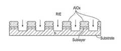
- FIG. 3Dthe structure of FIG. 3C is placed in an ALD chamber and exposed to chemical precursors that react only with one material in the pattern (in this example the oxidized PS).
- the chemical precursorsare a sequence of trimethyl aluminum, TMA and water
- the TMAwill react with the carbonyl groups in the oxidized PS and become infused into the PS material.
- the second water precursorreacts with the TMA to form an aluminum oxide (AlO x ), which is predominately alumina, in the PS.
- AlO xaluminum oxide
- the ALD processcan be repeated a number of cycles to form the desired amount of alumina film in the PS.
- FIG. 3Dit is possible to first run the ALD tool in “static mode”, also called as “sequential infiltration synthesis” (SIS), depicted in FIG. 3D , to infuse the TMA inside the oxidized PS, and then switch to conventional thermal ALD, wherein the substrate is heated, to increase the growth rate and to grow alumina films on top of the targeted PS, as depicted in FIG. 3E .
- the resulting chemical contrast pattern in FIGS. 3D and 3Emimics the original PS/PMMA pattern ( FIG. 3A ) with higher fidelity and higher continuity than the conventional SIS method.
- conventional SISthe features of alumina infiltrated in the PMMA ( FIG. 1D ) can be discontinuous after the removal of the PS/PMMA polymer matrix.
- the thickness of the PShas been reduced during the oxygen plasma RIE that oxidizes the PS, as shown by the reduced height of the PS from FIG. 3A to FIG. 3B .
- the conventional SIS methodbecause the alumina is infiltrated over the entire thickness of the PMMA in a rather low density matrix, the alumina is prone to deformation upon removal of the PMMA and PS.
- the aspect ratio (thickness to width) of the PMMA with infused alumina in conventional SISis fairly large, around 2:1, whereas the aspect ratio for the PS with infused alumina may be less than 1.
- FIGS. 4A-4Cillustrate the additional steps.
- the SMP bound to the substrateshown in FIGS. 3D and 3E
- RIEoxygen plasma
- FIG. 4Ba second RIE can be used to etch into the substrate, using the PS with alumina as an etch mask.
- a fluorine etchcan be used to etch features into the Si substrate.
- the remaining alumina and underlying PS materialcan be removed by RIE or a wet etch.
- the substratecould have suitable transfer layers, like a hard mask, between the substrate and the PS with alumina, to aid in transferring the chemical contrast pattern into the substrate.
- the resulting substrate with the etched patterncan be used as an imprint template.
- the chemical contrast patterncan be also used as a pattern for DSA of the same BCP that results in a more robust pattern for pattern transfer into a substrate, as compared to the conventional SIS method.
- the processis shown in FIGS. 5A-5E . This process starts from the chemical contrast pattern depicted either in FIG. 3D or 3 E.
- the pattern of SMP and PS with aluminadirect the self-assembly of a second BCP film.
- a thin film of a second BCPis spin coated on top of the chemical contrast pattern of the SMP and PS with alumina.
- the second BCPcan have the same or different components as the first BCP, but should have the same natural pitch (L 0 ) as the first BCP (like the example of FIG.
- the PS—OH brush (the SMP) bound to the substrateis preferentially wet by the PS of the second additional PS-b-PMMA BCP, whereas the alumina on the PS is preferentially wet by the additional PMMA.
- PMMAbeing a more polar molecule, preferentially wets the oxide interface, while PS preferentially wets the PS in the SMP.
- the second BCP componentsreplicate the pattern of the original underlying BCP components, but with a “phase shift”. In those regions where originally there was PS, now there is a PMMA, and vice versa.
- the chemical contrast pattern of the underlying SMP and PS with aluminadirects the self assembly of the additional PMMA and PS components into a periodic pattern that replicates the underlying chemical contrast pattern.
- FIG. 5Bthe structure is now exposed to ALD precursors for SIS.
- the TMA precursorselectively attaches to the carbonyl groups in the PMMA and is infused in the PMMA.
- a second precursorfor example water vapor, is introduced which completes the reaction, converting the TMA into alumina in the PMMA.
- the ALD cyclecan be repeated a number of times to increase the amount of infused alumina. As a result there is an upper pattern of PMMA with infused alumina directly above a lower pattern of PS with infused alumina.
- FIG. 1there is an upper pattern of PMMA with infused alumina directly above a lower pattern of PS with infused alumina.
- FIG. 5Cthe PS and PMMA is removed with RIE, condensing the infused alumina in the upper PMMA on top of the previously infused alumina in the lower PS.
- RIEetching the infused alumina in the upper PMMA on top of the previously infused alumina in the lower PS.
- the alumina featuresor other inorganic features remaining after RIE are not continuous, resulting in broken features or broken lines.
- the structure of FIG. 5Chas an important advantage over conventional SIS in that the second or upper alumina is deposited on top of the previously infused lower alumina. Thus even if the upper film of alumina is broken in certain sections, the lower alumina adds additional material to prevent a broken feature.
- a second RIEcan be used to etch into the substrate, using the alumina film as an etch mask.
- a fluorine etchcan be used to etch features into the Si substrate.
- the remaining alumina and underlying sublayer materialcan be removed by RIE or a wet etch.
- the substratecould have suitable transfer layers, like a hard mask, between the substrate and the alumina film, to aid in transferring the chemical contrast pattern into the substrate.
- the resulting substrate with the etched patterncan be used as an imprint template.
- the second BCPhas the same natural pitch (L 0 ) as the first BCP.
- density multiplication of the patterncan be achieved by use of a second BCP that has a natural pitch that is an integer fraction, for example 1 ⁇ 2, the natural pitch of the first BCP.
- the PS in the lower layerwould have a width one-half that shown in FIG. 5A . This would be achieved by continuing the O 2 RIE shown in FIG. 3B to remove additional PS material until the width of the PS features is reduced by one-half. With this pattern of reduced-width PS and SMP as the lower layer in FIG.
- the second BCP componentswould be directed to self-assemble with one PMMA feature on each reduced-width PS feature. This would cause alternating PS/PMMA/PS features to self-assemble on each lower SMP feature.
- the resulting chemical contrast patternwould look like that of FIG. 5C , but with double the density of AlOx features.
- the ALD precursorsare selected to infiltrate the inorganic material into one of the BCP components and to be non-reactive with the other BCP component.
- the inorganic materialis alumina and the precursors are TMA, which is reactive with the carbonyl groups in PMMA and non-reactive with PS, and water vapor.
- TMAreactive with the carbonyl groups in PMMA and non-reactive with PS
- other inorganic materials with suitable precursorsmay be formed by ALD.
- the inorganic materialis to be a titanium oxide (TiOx)
- the precursorsmay be tetrakis(dimethylamido)titanium (TDMAT) and water vapor.
- titanium containing precursorscould be used in conjunction with water, such as titanium tetrachloride (TiCl 4 ) and titanium butoxide (Ti(OBu) 4 ).
- TiCl 4titanium tetrachloride
- Ti(OBu) 4titanium butoxide
- the inorganic materialis to be ZnO then the precursors may be diethyl zinc and water. If the inorganic material is to be SiO 2 then the precursors may be tris(tert-pentoxy)silanol and water. If the inorganic material is to be tungsten (W), then the precursors may be tungsten hexafluoride and disilane.
- a first TMA/H 2 O cyclemay be used to grow a first film of alumina and then the alumina film is used to grow the film of the desired inorganic material in subsequent cycles.
Landscapes
- Chemical & Material Sciences (AREA)
- Physics & Mathematics (AREA)
- General Physics & Mathematics (AREA)
- Health & Medical Sciences (AREA)
- Chemical Kinetics & Catalysis (AREA)
- Medicinal Chemistry (AREA)
- Polymers & Plastics (AREA)
- Organic Chemistry (AREA)
- Exposure Of Semiconductors, Excluding Electron Or Ion Beam Exposure (AREA)
- Drying Of Semiconductors (AREA)
Abstract
Description
- 1. Field of the Invention
- This invention relates generally to the use of block copolymers (BCPs) to make a chemical contrast pattern, and more particularly to the use of the chemical contrast pattern as an etch mask for pattern transfer into a substrate.
- 2. Description of the Related Art
- Directed self-assembly (DSA) of block copolymers (BCPs) has been proposed for making imprint templates. Imprint templates have application in making patterned-media magnetic recording disks and in semiconductor manufacturing, for example, for patterning parallel generally straight lines in MPU, DRAM and NAND flash devices. DSA of BCPs by use of a patterned sublayer for the BCP film is well-known. After the BCP components self-assemble on the patterned sublayer, one of the components is selectively removed, leaving the other component with the desired pattern, which can be used as an etch mask to transfer the pattern into an underlying substrate. The etched substrate can be used as an imprint template.
- More recently a method termed “sequential infiltration synthesis” (SIS) uses a BCP and atomic layer deposition (ALD) to selectively grow nanometer scale patterns of inorganic material inside BCP. In SIS, a BCP film is deposited onto a substrate and annealed to form a self-assembled pattern of the two BCP components. In one example, the BCP is poly(styrene-block-methyl methacrylate) (PS-b-PMMA). A first precursor for the inorganic material is introduced into the ALD and infiltrates the PMMA but does not react with the PS. A second precursor for the inorganic material is then introduced to finish the reaction, forming the inorganic material, for example alumina (Al2O3), in the locations in the PMMA where the first precursor attached. The PS and PMMA are removed, leaving a pattern that generally replicates the original pattern of PS and PMMA but that is now made of the inorganic material synthesized by the ALD precursors. This pattern of inorganic material can then be used as an etch mask to etch the substrate.
- While the conventional SIS method provides a way to use the distinct chemistries of the constituent components of a BCP film to grow materials by ALD on specific locations, the density of active sites where the ALD precursor can bind is extremely low, especially when using the method to achieve dimensions down to a few nanometers. It has been found that after removal of all of the polymer material (the PS and PMMA in the above example), the amount of inorganic material (alumina in the above example) is not sufficient to make a robust etch mask. This is because the remaining features may be discontinuous or may have shifted as the PS and PMMA is removed, thus degrading the image quality of the original pattern.
- What is needed is a method for making a chemical contrast pattern with BCPs that uses SIS but that does not result in a pattern with discontinuous or shifted features.
- Embodiments of the invention relate to methods that use DSA of BCPs and take advantage of SIS to make a chemical contrast pattern. For the example with PS and PMMA as the BCP components, in contrast to the conventional SIS method, embodiments of the invention remove the PMMA prior to the ALD and makes the PS the active material for the ALD. The inorganic material grown by ALD in the active PS replicates the original pattern without major image quality distortions.
- In an example of the method that uses PS-b-PMMA as the BCP and alumina as the inorganic material, the PS and PMMA self-assemble on a patterned sublayer formed on a suitable substrate. The PMMA is removed to expose regions of the underlying substrate, leaving the PS on the substrate, after which the PS is oxidized. A surface modification polymer (SMP) having functional end groups is deposited on the oxidized PS and the exposed substrate regions and the SMP not bound to the substrate is removed. The substrate with the bound SMP and oxidized PS is then placed in an atomic layer deposition (ALD) chamber and the alumina precursors are introduced. The precursors are non-reactive with the SMP but reactive with the oxidized PS, so that alumina is formed in the oxidized PS, thereby forming on the substrate a chemical contrast pattern of SMP and alumina. The resulting chemical contrast pattern can be used for lithographic masks, for example to etch the underlying substrate to make an imprint template.
- The chemical contrast pattern can also be used as a pattern for DSA of additional BCP that results in a more robust pattern for pattern transfer into a substrate, as compared to the conventional SIS method. For the example where alumina is the inorganic material, the pattern of SMP and PS with alumina directs the self-assembly of a second upper BCP film. If the second BCP is also PS-b-PMMA, then the SMP bound to the substrate is preferentially wet by the PS of the second BCP, whereas the alumina on the first PS is preferentially wet by the second PMMA. In this case, the second upper BCP components replicate the pattern of the original underlying first BCP components, but with a “phase shift”, i.e., in those regions where originally there was PS, now there is a PMMA, and vice versa. Upon annealing, the chemical contrast pattern of the underlying SMP and PS with alumina directs the self assembly of the additional upper PMMA and PS components into a periodic pattern that replicates the underlying chemical contrast pattern. The structure is then placed in an ALD and exposed to the alumina precursors. The alumina now becomes infused into the second upper PMMA. As a result there is an upper pattern of PMMA with infused alumina directly above a lower pattern of PS with infused alumina. The PS and PMMA are removed, for example by reactive ion etching (RIE), condensing the infused alumina in the upper PMMA on top of the previously infused alumina in the lower PS. The resulting chemical contrast pattern can be used for lithographic masks, for example to etch the underlying substrate to make an imprint template.
- For a fuller understanding of the nature and advantages of the present invention, reference should be made to the following detailed description taken together with the accompanying figures.
FIGS. 1A-1D are view illustrating the prior art method for making an imprint template using directed self-assembly (DSA) of block copolymers (BCPs).FIGS. 2A-2F are side sectional views illustrating the prior art sequential infiltration synthesis (SIS) method using atomic layer deposition (ALD) and a BCP film.FIGS. 3A-3E are side sectional views illustrating embodiments of the invention to make a chemical contrast pattern using BCPs and SIS.FIGS. 4A-4C are side sectional views illustrating use of the chemical contrast pattern made according to embodiments of the invention as an etch mask for pattern transfer into a substrate.FIGS. 5A-5E are side sectional views illustrating use of the chemical contrast pattern made according to embodiments of the invention as a pattern for DSA of an additional BCP to create a more robust pattern as an etch mask for pattern transfer into a substrate.- Self-assembling block copolymers (BCPs) have been proposed for creating periodic nanometer (nm) scale features. Self-assembling BCPs typically contain two or more different polymeric block components, for example components A and B, that are immiscible with one another. Under suitable conditions, the two or more immiscible polymeric block components separate into two or more different phases or microdomains on a nanometer scale and thereby form ordered patterns of isolated nano-sized structural units. There are many types of BCPs that can be used for forming the self-assembled periodic patterns. If one of the components A or B is selectively removable without having to remove the other, then an orderly arranged structural units of the un-removed component can be formed.
- Specific examples of suitable BCPs that can be used for forming the self-assembled periodic patterns include, but are not limited to: poly(styrene-block-methyl methacrylate) (PS-b-PMMA), poly(ethylene oxide-block-isoprene) (PEO-b-PI), poly(ethylene oxide-block-butadiene) (PEO-b-PBD), poly(ethylene oxide-block-styrene) (PEO-b-PS), poly(ethylene oxide-block-methylmethacrylate) (PEO-b-PMMA), poly(ethyleneoxide-block-ethylethylene) (PEO-b-PEE), poly(styrene-block-vinylpyridine) (PS-b-PVP), poly(styrene-block-isoprene) (PS-b-PI), poly(styrene-block-butadiene) (PS-b-PBD), poly(styrene-block-ferrocenyldimethylsilane) (PS-b-PFS), poly(butadiene-block-vinylpyridine) (PBD-b-PVP), poly(isoprene-block-methyl methacrylate) (PI-b-PMMA), poly(styrene-block-lactic acid) (PS-b-PLA) and poly(styrene-block-dymethylsiloxane) (PS-b-PDMS).
- The specific self-assembled periodic patterns formed by the BCP are determined by the molecular volume ratio between the first and second polymeric block components A and B. When the ratio of the molecular volume of the second polymeric block component B over the molecular volume of the first polymeric block component A is less than about 80:20 but greater than about 60:40, the BCP will form an ordered array of cylinders composed of the first polymeric block component A in a matrix composed of the second polymeric block component B. When the ratio of the molecular volume of the first polymeric block component A over the molecular volume of the second polymeric block component B is less than about 60:40 but is greater than about 40:60, the BCP will form alternating lamellae composed of the first and second polymeric block components A and B. The un-removed component is used as an etch mask to etch the underlying template substrate. When the ratio of B over A is greater than about 80:20 the BCP will form an ordered array of spheres in a matrix of the second component. For lamellar or cylinder forming BCPs, the orientation of the lamellae or the cylinders with respect to the substrate depends on the interfacial energies (wetting properties) of the block copolymer components at both the substrate interface and at the top interface. When one of the block components preferentially wets the substrate (or the top free interface) the block copolymers form layers parallel to the substrate. When the wetting properties at the interface are neutral to either block, then both block components can be in contact with the interface, facilitating the formation of block copolymer domains with perpendicular orientation. In practice, the wetting properties of the substrate are engineered by coating the substrate with “surface modification layers” that tune the wetting properties at the interface. Surface modification layers are usually made of polymer brushes or mats typically (but not necessarily) composed of a mixture of the constituent block materials of the BCP to be used.
- The periodicity or natural pitch (L0) of the repeating structural units in the periodic pattern is determined by intrinsic polymeric properties such as the degree of polymerization N and the Flory-Huggins interaction parameter χ. L0scales with the degree of polymerization N, which in turn correlates with the molecular weight M. Therefore, by adjusting the total molecular weight of the BCP, the natural pitch (L0) of the repeating structural units can be selected.
- To form the self-assembled periodic patterns, the BCP is first dissolved in a suitable solvent system to form a BCP solution, which is then applied onto a surface to form a thin BCP layer, followed by annealing of the thin BCP layer, which causes phase separation between the different polymeric block components contained in the BCP. The solvent system used for dissolving the BCP and forming the BCP solution may comprise any suitable non-polar solvent, including, but not limited to: toluene, propylene glycol monomethyl ether acetate (PGMEA), propylene glycol monomethyl ether (PGME), and acetone. The BCP solution can be applied to the substrate surface by any suitable techniques, including, but not limited to: spin casting, coating, spraying, ink coating, dip coating, etc. Preferably, the BCP solution is spin cast onto the substrate surface to form a thin BCP layer. After application of the thin BCP layer onto the substrate surface, the entire substrate is annealed to effectuate microphase segregation of the different block components contained by the BCP, thereby forming the periodic patterns with repeating structural units.
- The BCP films in the above-described techniques self-assemble without any direction or guidance. This undirected self-assembly results in patterns with defects so it is not practical for applications that require long-range ordering, such as for making imprint templates. However, directed self-assembly (DSA) of block copolymers (BCPs) has been proposed for making imprint templates. DSA of BCPs by use of a patterned sublayer for the BCP film is well-known, as described for example in U.S. Pat. No. 7,976,715; U.S. Pat. No. 8,059,350; and U.S. Pat. No. 8,119,017. Pending application Ser. No. 13/627,492, filed Sep. 26, 2012 and assigned to the same assignee as this application, describes the use DSA of BCPs to make two submaster imprint templates, one with a pattern of generally radial lines, and the other with generally concentric rings, to make a master imprint template, which is then used to imprint patterned-media magnetic recording disks. Imprint templates made with DSA of BCPs have also been proposed for use in semiconductor manufacturing, for example, for patterning parallel generally straight lines in MPU, DRAM and NAND flash devices.
- The prior art method for making an imprint template using DSA of BCPs will be described in general terms with
FIGS. 1A-1D for an example where thetemplate 50 will become an imprint template withprotrusions 51 in a pattern of parallel bars.FIG. 1A is a side sectional view showing apatterned sublayer 105 on the surface oftemplate 50. Alternating A component (polystyrene—PS)parallel lines 112 and B component (PMMA)parallel lines 115 are formed on asublayer 105 andregions 106. Theregions 106 can be exposed portions of thetemplate 50 not covered bysublayer 105 or regions covered by a different sublayer. Thesublayer 105 has been patterned to direct the self-assembly of the BCP A and B components with a natural pitch of L0. InFIG. 1B , the portions ofparallel lines 115, the B component (PMMA), are then selectively removed by a wet etch or a dry etch process. This leaves generallyparallel lines 112 of the A component (PS) on thetemplate 50. Then, a dry etch process is used to etch thetemplate 50 to formrecesses 52 using theparallel lines 112 as the etch mask. The material ofparallel lines 112 and the remainingunderlying sublayer 105 is then removed, leavingrecesses 52 intemplate 50. This leaves the structure as shown inFIG. 1C , with a pattern of protrusions formed asparallel bars 51 and recesses formed asparallel bars 52.FIG. 1D is a side sectional view of the resulting imprint template. - More recently a method termed “sequential infiltration synthesis” (SIS) uses BCP films and atomic layer deposition (ALD) to selectively grow nanometer scale patterns of inorganic material inside BCP films. (See Peng et al., “A Route to Nanoscopic Materials via Sequential Infiltration Synthesis on Block Copolymer Templates”,ACS Nano, VOL. 5, NO. 6, 4600-4606, 2011). This process is depicted in
FIGS. 2A-2F . In SIS, a BCP film is deposited onto a substrate and annealed to form a self-assembled pattern, for example PS and PMMA (FIG. 1A ). The sample is then placed in an ALD chamber, such as those available from Cambridge Nanotech Inc. of Cambridge, Mass. ALD is known as a process for forming very thin films on a substrate. ALD involves deposition of gas phase precursor molecules. Most ALD processes are based on binary reaction sequences where two surface reactions occur and deposit a binary compound film, such as the use of trimethylaluminum (TMA) and H2O to form alumina (Al2O3). An overview of ALD is presented by George, “Atomic Layer Deposition: An Overview”,Chemical Review,2010, Vol. 110, No. 1, 111-131. In SIS, the BCP has been chosen so that one component, for example PS, is inert to the ALD precursors while the other component, PMMA, reacts with the precursor. A first precursor, for example TMA, is introduced into the ALD chamber (FIG. 2B ). PMMA contains carbonyl groups that react with the TMA, causing the TMA to infiltrate the PMMA. The controlled interaction of TMA with carbonyl groups in the PMMA generates Al—CH3/Al—OH sites inside the PMMA. A second precursor, for example water vapor, is then introduced to finish the reaction, forming alumina in the locations in the PMMA where the TMA attached (FIG. 2C ). The processes may be repeated a number of cycles to increase the amount of infiltrated alumina. For lithographic applications, the PS component, which is inert to the ALD precursors, and the PMMA material is then removed by oxygen plasma to leave a pattern that mimics the original pattern of PS and PMMA but that is now made of the alumina synthesized by the ALD precursors (FIG. 2D ). This pattern of alumina can then be used as an etch mask to reactively ion etch (RIE) the substrate (FIG. 2E ), after which the alumina is removed, leaving the etched substrate (FIG. 2F ). - While the conventional SIS method provides a way to use the distinct chemistries of the constituent components of a BCP film to grow materials by ALD on specific locations, the density of active sites where the ALD precursor can bind is extremely low, especially when using the method to achieve dimensions down to a few nanometers. It has been found that after removal of all of the polymer material (the PS and PMMA in the above example), the amount of inorganic material (alumina in the above example) is not sufficient to make a robust etch mask. This is because the remaining features may be discontinuous or may have shifted as the PS and PMMA is removed, thus degrading the image quality of the original pattern. This is described by R. Ruiz, et al.,Journal of Vacuum Science&Technology B: Microelectronics and Nanometer Structures,2012, 30, (6).
- Embodiments of the invention use DSA of BCPs and take advantage of SIS to make a chemical contrast pattern. For the example with PS and PMMA as the BCP components, in contrast to the conventional SIS method, an embodiment of the invention removes the PMMA prior to the ALD and makes the PS the active material for the ALD. The inorganic material grown by ALD in the active PS replicates the original pattern without major image quality distortions. The resulting chemical contrast pattern can be used for lithographic masks, for example to etch the underlying substrate to make an imprint template, or as a chemical contrast pattern to guide the growth of other materials, such as in DSA.
- An embodiment of the invention is illustrated in
FIGS. 3A-3E .FIG. 3A is a cross-sectional view of a BCP film that has been directed to self-assemble into PMMA and PS by a patterned sublayer on a suitable substrate, in this example a silicon (Si) substrate that may have a silicon oxide surface. The substrate may be formed of any suitable material, such as, but not limited to, single-crystal Si, amorphous Si, silica, fused quartz, silicon nitride, carbon, tantalum, molybdenum, chromium, alumina and sapphire. The sublayer may be a nearly neutral layer of a material that does not show a strong wetting affinity by one of the polymer blocks over the other. The neutral layer can be, but is not restricted to, a functionalized polymer brush like carboxyl-terminated or hydroxyl-terminated brush, a cross-linkable polymer, a functionalized polymer “A” or “B” or a functionalized random copolymer “A-r-B”. The functional group may be, for example, a hydroxyl (OH) group. In the present example, the substrate has a silicon oxide surface film and the neutral layer is a hydroxyl-terminated poly(styrene-r-methyl methacrylate) brush containing ˜67% styrene. Alternatively, the sublayer may be a material known as a polymer “mat” layer that shows strong wetting affinity by one of the polymer blocks over the other. The material of mat layer can be, but is not limited to, a cross-linkable polymer “A” or “B” like a crosslinkable polystyrene (XPS mat). The sublayer material may be spin-coated on the substrate to a thickness of about 1-10 nm. The sublayer is annealed for the end-groups to graft to the oxidized substrate surface in the case of an end-functionalized material or for the cross linking units to carry the cross-linking in the case of polymer “mats”. After annealing, any ungrafted sublayer material is rinsed away in a suitable solvent (toluene, PGMA, NMP, etc). The purpose of the sublayer is to tune the surface energy adequately to promote the desired domain orientation (for example, perpendicular lamellae of the BCP components). - For DSA, additional steps are required to create a chemical pattern in the sublayer. These steps may include e-beam lithography, photolithography or nanoimprint lithography and potentially a combination of polymer mats and brushes. For example, a resist layer can be patterned by e-beam, followed by deposition of the sublayer material and removal of the resist. Alternatively, the chemical structure of exposed portions of a neutral sublayer can be chemically damaged or altered (by oxygen plasma etching or other process such as RIE, neutral atom (such as Ar) or molecule milling, ion bombardment and photodegradation) so that the exposed portions of the neutral sublayer have a preferred affinity (or repulsion) for one of the BCP components.
- The resulting pattern of the sublayer directs the BCP components to self-assemble according to the pattern. The BCP is chosen to form either lamellae, cylinders or spheres with a characteristic center-to-center distance or “natural pitch” L0in the range of 5-50 nm.
FIG. 3A shows an example of lamellae-forming poly(styrene-block-methyl methacrylate) (PS-b-PMMA) BCP for which the OH-terminated brush neutral layer was chosen as the sublayer to promote perpendicular orientation of the lamellar domains. - In
FIG. 3B one of the two BCP components is selectively removed, for example by reactive ion etching (RIE), wet etching, or ion milling. In the example ofFIG. 3B , the PMMA and the underlying sublayer regions have been removed by oxygen plasma RIE. The remaining component, in this example the PS, needs to be chemically active to react with the ALD precursors. The remaining component material may naturally contain active groups, such as carbonyl or hydroxyl groups, or it's chemistry may be altered, for example by an oxygen plasma and/or UV radiation, to render the material active for reaction with the ALD precursors. In the example ofFIG. 3B , the PMMA component is removed by RIE with an oxygen plasma. The oxygen plasma also simultaneously oxidizes the remaining PS, creating active groups, including carbonyl groups, that can react with the ALD precursors. An additional UV curing step may be applied to further harden the remaining PS material. - Next, in
FIG. 3C , a layer of a surface modification polymer (SMP) with functionalized groups is applied onto the substrate with the PS and annealed. The SMP is chosen from a material that is generally inert to the ALD precursors. The functionalized groups of the SMP are chosen to chemically bind with the exposed portions of the substrate, but not with the remaining BCP component. In the example ofFIG. 3C , where the substrate is a Si substrate with a native SiOxsurface, the SMP is a PS—OH brush for which the OH functional groups bind to the SiOxsurface after thermal annealing. After annealing, the excess brush material that is not bound to the substrate can be rinsed away. The resulting pattern consists of features that are chemically prone to react with the ALD precursors (in this example, the PS modified by the oxygen plasma) and features that are chemically inert to the ALD precursors (the SMP bound to the substrate). - In
FIG. 3D the structure ofFIG. 3C is placed in an ALD chamber and exposed to chemical precursors that react only with one material in the pattern (in this example the oxidized PS). For example, if the chemical precursors are a sequence of trimethyl aluminum, TMA and water, the TMA will react with the carbonyl groups in the oxidized PS and become infused into the PS material. The second water precursor reacts with the TMA to form an aluminum oxide (AlOx), which is predominately alumina, in the PS. The ALD process can be repeated a number of cycles to form the desired amount of alumina film in the PS. It is possible to first run the ALD tool in “static mode”, also called as “sequential infiltration synthesis” (SIS), depicted inFIG. 3D , to infuse the TMA inside the oxidized PS, and then switch to conventional thermal ALD, wherein the substrate is heated, to increase the growth rate and to grow alumina films on top of the targeted PS, as depicted inFIG. 3E . The resulting chemical contrast pattern inFIGS. 3D and 3E mimics the original PS/PMMA pattern (FIG. 3A ) with higher fidelity and higher continuity than the conventional SIS method. In conventional SIS, the features of alumina infiltrated in the PMMA (FIG. 1D ) can be discontinuous after the removal of the PS/PMMA polymer matrix. InFIG. 3D , the thickness of the PS has been reduced during the oxygen plasma RIE that oxidizes the PS, as shown by the reduced height of the PS fromFIG. 3A toFIG. 3B . This places the alumina closer to the substrate than conventional SIS, making it less prone to mechanical deformations when the PMMA is removed. In the conventional SIS method, because the alumina is infiltrated over the entire thickness of the PMMA in a rather low density matrix, the alumina is prone to deformation upon removal of the PMMA and PS. The aspect ratio (thickness to width) of the PMMA with infused alumina in conventional SIS is fairly large, around 2:1, whereas the aspect ratio for the PS with infused alumina may be less than 1. - The chemical contrast pattern depicted in
FIG. 3D or3E can be used as an etch mask for pattern transfer.FIGS. 4A-4C illustrate the additional steps. InFIG. 4A , the SMP bound to the substrate (shown inFIGS. 3D and 3E ), i.e., the PS—OH brush layer material in the regions between the PS with alumina that did not react with the ALD precursors, is selectively removed by RIE in an oxygen plasma. InFIG. 4B , a second RIE can be used to etch into the substrate, using the PS with alumina as an etch mask. In the example with a Si substrate and alumina on the PS, a fluorine etch can be used to etch features into the Si substrate. InFIG. 4C , the remaining alumina and underlying PS material can be removed by RIE or a wet etch. Alternatively, the substrate could have suitable transfer layers, like a hard mask, between the substrate and the PS with alumina, to aid in transferring the chemical contrast pattern into the substrate. The resulting substrate with the etched pattern can be used as an imprint template. - The chemical contrast pattern can be also used as a pattern for DSA of the same BCP that results in a more robust pattern for pattern transfer into a substrate, as compared to the conventional SIS method. The process is shown in
FIGS. 5A-5E . This process starts from the chemical contrast pattern depicted either inFIG. 3D or3E. The pattern of SMP and PS with alumina direct the self-assembly of a second BCP film. InFIG. 5A a thin film of a second BCP is spin coated on top of the chemical contrast pattern of the SMP and PS with alumina. The second BCP can have the same or different components as the first BCP, but should have the same natural pitch (L0) as the first BCP (like the example ofFIG. 5A ) or a natural pitch that is an integer fraction, for example ½, the natural pitch of the first BCP. In the example shown inFIG. 5A , the PS—OH brush (the SMP) bound to the substrate is preferentially wet by the PS of the second additional PS-b-PMMA BCP, whereas the alumina on the PS is preferentially wet by the additional PMMA. This is because PMMA, being a more polar molecule, preferentially wets the oxide interface, while PS preferentially wets the PS in the SMP. In this case, the second BCP components replicate the pattern of the original underlying BCP components, but with a “phase shift”. In those regions where originally there was PS, now there is a PMMA, and vice versa. Upon annealing, the chemical contrast pattern of the underlying SMP and PS with alumina directs the self assembly of the additional PMMA and PS components into a periodic pattern that replicates the underlying chemical contrast pattern. InFIG. 5B , the structure is now exposed to ALD precursors for SIS. The TMA precursor selectively attaches to the carbonyl groups in the PMMA and is infused in the PMMA. A second precursor, for example water vapor, is introduced which completes the reaction, converting the TMA into alumina in the PMMA. The ALD cycle can be repeated a number of times to increase the amount of infused alumina. As a result there is an upper pattern of PMMA with infused alumina directly above a lower pattern of PS with infused alumina. InFIG. 5C the PS and PMMA is removed with RIE, condensing the infused alumina in the upper PMMA on top of the previously infused alumina in the lower PS. In conventional SIS it is common that the alumina features (or other inorganic features) remaining after RIE are not continuous, resulting in broken features or broken lines. The structure ofFIG. 5C has an important advantage over conventional SIS in that the second or upper alumina is deposited on top of the previously infused lower alumina. Thus even if the upper film of alumina is broken in certain sections, the lower alumina adds additional material to prevent a broken feature. InFIG. 5D , a second RIE can be used to etch into the substrate, using the alumina film as an etch mask. In the example with a Si substrate and alumina film as the inorganic material, a fluorine etch can be used to etch features into the Si substrate. InFIG. 5E , the remaining alumina and underlying sublayer material can be removed by RIE or a wet etch. Alternatively, the substrate could have suitable transfer layers, like a hard mask, between the substrate and the alumina film, to aid in transferring the chemical contrast pattern into the substrate. The resulting substrate with the etched pattern can be used as an imprint template. - In the example of
FIGS. 5A-5E , the second BCP has the same natural pitch (L0) as the first BCP. However, density multiplication of the pattern can be achieved by use of a second BCP that has a natural pitch that is an integer fraction, for example ½, the natural pitch of the first BCP. In such an embodiment to double the density, the PS in the lower layer would have a width one-half that shown inFIG. 5A . This would be achieved by continuing the O2RIE shown inFIG. 3B to remove additional PS material until the width of the PS features is reduced by one-half. With this pattern of reduced-width PS and SMP as the lower layer inFIG. 5A , the second BCP components would be directed to self-assemble with one PMMA feature on each reduced-width PS feature. This would cause alternating PS/PMMA/PS features to self-assemble on each lower SMP feature. The resulting chemical contrast pattern would look like that ofFIG. 5C , but with double the density of AlOx features. - The ALD precursors are selected to infiltrate the inorganic material into one of the BCP components and to be non-reactive with the other BCP component. In the examples above the inorganic material is alumina and the precursors are TMA, which is reactive with the carbonyl groups in PMMA and non-reactive with PS, and water vapor. However, other inorganic materials with suitable precursors may be formed by ALD. For example, if the inorganic material is to be a titanium oxide (TiOx), the precursors may be tetrakis(dimethylamido)titanium (TDMAT) and water vapor. Alternatively, other titanium containing precursors could be used in conjunction with water, such as titanium tetrachloride (TiCl4) and titanium butoxide (Ti(OBu)4). If the inorganic material is to be ZnO then the precursors may be diethyl zinc and water. If the inorganic material is to be SiO2then the precursors may be tris(tert-pentoxy)silanol and water. If the inorganic material is to be tungsten (W), then the precursors may be tungsten hexafluoride and disilane. In some of these examples, if the first precursor for the desired inorganic material does not readily react with the BCP component, a first TMA/H2O cycle may be used to grow a first film of alumina and then the alumina film is used to grow the film of the desired inorganic material in subsequent cycles.
- While the present invention has been particularly shown and described with reference to the preferred embodiments, it will be understood by those skilled in the art that various changes in form and detail may be made without departing from the spirit and scope of the invention. Accordingly, the disclosed invention is to be considered merely as illustrative and limited in scope only as specified in the appended claims.
Claims (23)
Priority Applications (1)
| Application Number | Priority Date | Filing Date | Title |
|---|---|---|---|
| US13/902,795US8900467B1 (en) | 2013-05-25 | 2013-05-25 | Method for making a chemical contrast pattern using block copolymers and sequential infiltration synthesis |
Applications Claiming Priority (1)
| Application Number | Priority Date | Filing Date | Title |
|---|---|---|---|
| US13/902,795US8900467B1 (en) | 2013-05-25 | 2013-05-25 | Method for making a chemical contrast pattern using block copolymers and sequential infiltration synthesis |
Publications (2)
| Publication Number | Publication Date |
|---|---|
| US20140346142A1true US20140346142A1 (en) | 2014-11-27 |
| US8900467B1 US8900467B1 (en) | 2014-12-02 |
Family
ID=51934679
Family Applications (1)
| Application Number | Title | Priority Date | Filing Date |
|---|---|---|---|
| US13/902,795Active2033-06-14US8900467B1 (en) | 2013-05-25 | 2013-05-25 | Method for making a chemical contrast pattern using block copolymers and sequential infiltration synthesis |
Country Status (1)
| Country | Link |
|---|---|
| US (1) | US8900467B1 (en) |
Cited By (366)
| Publication number | Priority date | Publication date | Assignee | Title |
|---|---|---|---|---|
| US20150162195A1 (en)* | 2013-12-06 | 2015-06-11 | Samsung Electronics Co., Ltd. | Method of manufacturing a semiconductor device using purified block copolymers and semiconductor devices |
| JP2016108445A (en)* | 2014-12-05 | 2016-06-20 | 東京応化工業株式会社 | Substrate agent and manufacturing method of structure containing phase separation structure |
| US9508562B2 (en)* | 2014-06-27 | 2016-11-29 | Globalfoundries Inc. | Sidewall image templates for directed self-assembly materials |
| CN107104038A (en)* | 2016-02-19 | 2017-08-29 | Imec 非营利协会 | Patterns hardened with metallic or ceramic materials |
| US20170321025A1 (en)* | 2015-02-19 | 2017-11-09 | International Business Machines Corporation | Hybrid topographical and chemical pre-patterns for directed self-assembly of block copolymers |
| US9881793B2 (en) | 2015-07-23 | 2018-01-30 | International Business Machines Corporation | Neutral hard mask and its application to graphoepitaxy-based directed self-assembly (DSA) patterning |
| US9887135B1 (en) | 2017-04-28 | 2018-02-06 | Globalfoundries Inc. | Methods for providing variable feature widths in a self-aligned spacer-mask patterning process |
| WO2018109554A1 (en)* | 2016-12-15 | 2018-06-21 | Asm Ip Holding B.V. | Method of forming a structure on a substrate |
| US20180173109A1 (en)* | 2016-12-15 | 2018-06-21 | Imec Vzw | Lithographic Mask Layer |
| US20180171475A1 (en)* | 2016-12-15 | 2018-06-21 | Asm Ip Holding B.V. | Sequential infiltration synthesis apparatus and a method of forming a patterned structure |
| US10229833B2 (en) | 2016-11-01 | 2019-03-12 | Asm Ip Holding B.V. | Methods for forming a transition metal nitride film on a substrate by atomic layer deposition and related semiconductor device structures |
| US10249524B2 (en) | 2017-08-09 | 2019-04-02 | Asm Ip Holding B.V. | Cassette holder assembly for a substrate cassette and holding member for use in such assembly |
| US10249577B2 (en) | 2016-05-17 | 2019-04-02 | Asm Ip Holding B.V. | Method of forming metal interconnection and method of fabricating semiconductor apparatus using the method |
| US10262859B2 (en) | 2016-03-24 | 2019-04-16 | Asm Ip Holding B.V. | Process for forming a film on a substrate using multi-port injection assemblies |
| US10269558B2 (en) | 2016-12-22 | 2019-04-23 | Asm Ip Holding B.V. | Method of forming a structure on a substrate |
| US10276355B2 (en) | 2015-03-12 | 2019-04-30 | Asm Ip Holding B.V. | Multi-zone reactor, system including the reactor, and method of using the same |
| US10283353B2 (en) | 2017-03-29 | 2019-05-07 | Asm Ip Holding B.V. | Method of reforming insulating film deposited on substrate with recess pattern |
| US10290508B1 (en) | 2017-12-05 | 2019-05-14 | Asm Ip Holding B.V. | Method for forming vertical spacers for spacer-defined patterning |
| US10312055B2 (en) | 2017-07-26 | 2019-06-04 | Asm Ip Holding B.V. | Method of depositing film by PEALD using negative bias |
| US10312129B2 (en) | 2015-09-29 | 2019-06-04 | Asm Ip Holding B.V. | Variable adjustment for precise matching of multiple chamber cavity housings |
| US10319588B2 (en) | 2017-10-10 | 2019-06-11 | Asm Ip Holding B.V. | Method for depositing a metal chalcogenide on a substrate by cyclical deposition |
| US10319590B2 (en)* | 2015-12-23 | 2019-06-11 | Samsung Electronics Co., Ltd. | Method of forming semiconductor device using metal-containing hardmask to pattern photoresist having protected polymer |
| US10322384B2 (en) | 2015-11-09 | 2019-06-18 | Asm Ip Holding B.V. | Counter flow mixer for process chamber |
| US10340125B2 (en) | 2013-03-08 | 2019-07-02 | Asm Ip Holding B.V. | Pulsed remote plasma method and system |
| US10340135B2 (en) | 2016-11-28 | 2019-07-02 | Asm Ip Holding B.V. | Method of topologically restricted plasma-enhanced cyclic deposition of silicon or metal nitride |
| US10343920B2 (en) | 2016-03-18 | 2019-07-09 | Asm Ip Holding B.V. | Aligned carbon nanotubes |
| US10361201B2 (en) | 2013-09-27 | 2019-07-23 | Asm Ip Holding B.V. | Semiconductor structure and device formed using selective epitaxial process |
| US10366864B2 (en) | 2013-03-08 | 2019-07-30 | Asm Ip Holding B.V. | Method and system for in-situ formation of intermediate reactive species |
| US10364493B2 (en) | 2016-08-25 | 2019-07-30 | Asm Ip Holding B.V. | Exhaust apparatus and substrate processing apparatus having an exhaust line with a first ring having at least one hole on a lateral side thereof placed in the exhaust line |
| US10364496B2 (en) | 2011-06-27 | 2019-07-30 | Asm Ip Holding B.V. | Dual section module having shared and unshared mass flow controllers |
| US10367080B2 (en) | 2016-05-02 | 2019-07-30 | Asm Ip Holding B.V. | Method of forming a germanium oxynitride film |
| US10381219B1 (en) | 2018-10-25 | 2019-08-13 | Asm Ip Holding B.V. | Methods for forming a silicon nitride film |
| US10381226B2 (en) | 2016-07-27 | 2019-08-13 | Asm Ip Holding B.V. | Method of processing substrate |
| US10378106B2 (en) | 2008-11-14 | 2019-08-13 | Asm Ip Holding B.V. | Method of forming insulation film by modified PEALD |
| US10388513B1 (en) | 2018-07-03 | 2019-08-20 | Asm Ip Holding B.V. | Method for depositing silicon-free carbon-containing film as gap-fill layer by pulse plasma-assisted deposition |
| US10388509B2 (en) | 2016-06-28 | 2019-08-20 | Asm Ip Holding B.V. | Formation of epitaxial layers via dislocation filtering |
| US10395919B2 (en) | 2016-07-28 | 2019-08-27 | Asm Ip Holding B.V. | Method and apparatus for filling a gap |
| US10403504B2 (en) | 2017-10-05 | 2019-09-03 | Asm Ip Holding B.V. | Method for selectively depositing a metallic film on a substrate |
| US10410943B2 (en) | 2016-10-13 | 2019-09-10 | Asm Ip Holding B.V. | Method for passivating a surface of a semiconductor and related systems |
| US10435790B2 (en) | 2016-11-01 | 2019-10-08 | Asm Ip Holding B.V. | Method of subatmospheric plasma-enhanced ALD using capacitively coupled electrodes with narrow gap |
| US10438965B2 (en) | 2014-12-22 | 2019-10-08 | Asm Ip Holding B.V. | Semiconductor device and manufacturing method thereof |
| US10446393B2 (en) | 2017-05-08 | 2019-10-15 | Asm Ip Holding B.V. | Methods for forming silicon-containing epitaxial layers and related semiconductor device structures |
| US10458018B2 (en) | 2015-06-26 | 2019-10-29 | Asm Ip Holding B.V. | Structures including metal carbide material, devices including the structures, and methods of forming same |
| US10468262B2 (en) | 2017-02-15 | 2019-11-05 | Asm Ip Holding B.V. | Methods for forming a metallic film on a substrate by a cyclical deposition and related semiconductor device structures |
| US10468251B2 (en) | 2016-02-19 | 2019-11-05 | Asm Ip Holding B.V. | Method for forming spacers using silicon nitride film for spacer-defined multiple patterning |
| US10480072B2 (en) | 2009-04-06 | 2019-11-19 | Asm Ip Holding B.V. | Semiconductor processing reactor and components thereof |
| US10483099B1 (en) | 2018-07-26 | 2019-11-19 | Asm Ip Holding B.V. | Method for forming thermally stable organosilicon polymer film |
| US10504742B2 (en) | 2017-05-31 | 2019-12-10 | Asm Ip Holding B.V. | Method of atomic layer etching using hydrogen plasma |
| US10501866B2 (en) | 2016-03-09 | 2019-12-10 | Asm Ip Holding B.V. | Gas distribution apparatus for improved film uniformity in an epitaxial system |
| TWI679255B (en)* | 2014-12-05 | 2019-12-11 | 日商東京應化工業股份有限公司 | Brush composition, and method of producing structure containing phase-separated structure |
| US10510536B2 (en) | 2018-03-29 | 2019-12-17 | Asm Ip Holding B.V. | Method of depositing a co-doped polysilicon film on a surface of a substrate within a reaction chamber |
| US10529563B2 (en) | 2017-03-29 | 2020-01-07 | Asm Ip Holdings B.V. | Method for forming doped metal oxide films on a substrate by cyclical deposition and related semiconductor device structures |
| US10529554B2 (en) | 2016-02-19 | 2020-01-07 | Asm Ip Holding B.V. | Method for forming silicon nitride film selectively on sidewalls or flat surfaces of trenches |
| US10529542B2 (en) | 2015-03-11 | 2020-01-07 | Asm Ip Holdings B.V. | Cross-flow reactor and method |
| US10535516B2 (en) | 2018-02-01 | 2020-01-14 | Asm Ip Holdings B.V. | Method for depositing a semiconductor structure on a surface of a substrate and related semiconductor structures |
| US10541173B2 (en) | 2016-07-08 | 2020-01-21 | Asm Ip Holding B.V. | Selective deposition method to form air gaps |
| US10541333B2 (en) | 2017-07-19 | 2020-01-21 | Asm Ip Holding B.V. | Method for depositing a group IV semiconductor and related semiconductor device structures |
| WO2020020972A1 (en) | 2018-07-24 | 2020-01-30 | Cic Nanogune - Asociación Centro De Investigación Cooperativa En Nanociencias | Method for producing organic-inorganic hybrid materials |
| US10559458B1 (en) | 2018-11-26 | 2020-02-11 | Asm Ip Holding B.V. | Method of forming oxynitride film |
| US10561975B2 (en) | 2014-10-07 | 2020-02-18 | Asm Ip Holdings B.V. | Variable conductance gas distribution apparatus and method |
| US10566223B2 (en) | 2012-08-28 | 2020-02-18 | Asm Ip Holdings B.V. | Systems and methods for dynamic semiconductor process scheduling |
| US10590535B2 (en) | 2017-07-26 | 2020-03-17 | Asm Ip Holdings B.V. | Chemical treatment, deposition and/or infiltration apparatus and method for using the same |
| US10600673B2 (en) | 2015-07-07 | 2020-03-24 | Asm Ip Holding B.V. | Magnetic susceptor to baseplate seal |
| US10604847B2 (en) | 2014-03-18 | 2020-03-31 | Asm Ip Holding B.V. | Gas distribution system, reactor including the system, and methods of using the same |
| US10605530B2 (en) | 2017-07-26 | 2020-03-31 | Asm Ip Holding B.V. | Assembly of a liner and a flange for a vertical furnace as well as the liner and the vertical furnace |
| US10607895B2 (en) | 2017-09-18 | 2020-03-31 | Asm Ip Holdings B.V. | Method for forming a semiconductor device structure comprising a gate fill metal |
| USD880437S1 (en) | 2018-02-01 | 2020-04-07 | Asm Ip Holding B.V. | Gas supply plate for semiconductor manufacturing apparatus |
| US10612136B2 (en) | 2018-06-29 | 2020-04-07 | ASM IP Holding, B.V. | Temperature-controlled flange and reactor system including same |
| US10612137B2 (en) | 2016-07-08 | 2020-04-07 | Asm Ip Holdings B.V. | Organic reactants for atomic layer deposition |
| US10622375B2 (en) | 2016-11-07 | 2020-04-14 | Asm Ip Holding B.V. | Method of processing a substrate and a device manufactured by using the method |
| US10643904B2 (en) | 2016-11-01 | 2020-05-05 | Asm Ip Holdings B.V. | Methods for forming a semiconductor device and related semiconductor device structures |
| US10643826B2 (en) | 2016-10-26 | 2020-05-05 | Asm Ip Holdings B.V. | Methods for thermally calibrating reaction chambers |
| US10655221B2 (en) | 2017-02-09 | 2020-05-19 | Asm Ip Holding B.V. | Method for depositing oxide film by thermal ALD and PEALD |
| US10658181B2 (en) | 2018-02-20 | 2020-05-19 | Asm Ip Holding B.V. | Method of spacer-defined direct patterning in semiconductor fabrication |
| US10658205B2 (en) | 2017-09-28 | 2020-05-19 | Asm Ip Holdings B.V. | Chemical dispensing apparatus and methods for dispensing a chemical to a reaction chamber |
| US10665452B2 (en) | 2016-05-02 | 2020-05-26 | Asm Ip Holdings B.V. | Source/drain performance through conformal solid state doping |
| US10685834B2 (en) | 2017-07-05 | 2020-06-16 | Asm Ip Holdings B.V. | Methods for forming a silicon germanium tin layer and related semiconductor device structures |
| US10683571B2 (en) | 2014-02-25 | 2020-06-16 | Asm Ip Holding B.V. | Gas supply manifold and method of supplying gases to chamber using same |
| US10692741B2 (en) | 2017-08-08 | 2020-06-23 | Asm Ip Holdings B.V. | Radiation shield |
| US10707106B2 (en) | 2011-06-06 | 2020-07-07 | Asm Ip Holding B.V. | High-throughput semiconductor-processing apparatus equipped with multiple dual-chamber modules |
| US10714315B2 (en) | 2012-10-12 | 2020-07-14 | Asm Ip Holdings B.V. | Semiconductor reaction chamber showerhead |
| US10714350B2 (en) | 2016-11-01 | 2020-07-14 | ASM IP Holdings, B.V. | Methods for forming a transition metal niobium nitride film on a substrate by atomic layer deposition and related semiconductor device structures |
| US10714335B2 (en) | 2017-04-25 | 2020-07-14 | Asm Ip Holding B.V. | Method of depositing thin film and method of manufacturing semiconductor device |
| US10714385B2 (en) | 2016-07-19 | 2020-07-14 | Asm Ip Holding B.V. | Selective deposition of tungsten |
| US10734497B2 (en) | 2017-07-18 | 2020-08-04 | Asm Ip Holding B.V. | Methods for forming a semiconductor device structure and related semiconductor device structures |
| US10731249B2 (en) | 2018-02-15 | 2020-08-04 | Asm Ip Holding B.V. | Method of forming a transition metal containing film on a substrate by a cyclical deposition process, a method for supplying a transition metal halide compound to a reaction chamber, and related vapor deposition apparatus |
| US10734244B2 (en) | 2017-11-16 | 2020-08-04 | Asm Ip Holding B.V. | Method of processing a substrate and a device manufactured by the same |
| US10741385B2 (en) | 2016-07-28 | 2020-08-11 | Asm Ip Holding B.V. | Method and apparatus for filling a gap |
| US10755922B2 (en) | 2018-07-03 | 2020-08-25 | Asm Ip Holding B.V. | Method for depositing silicon-free carbon-containing film as gap-fill layer by pulse plasma-assisted deposition |
| US10767789B2 (en) | 2018-07-16 | 2020-09-08 | Asm Ip Holding B.V. | Diaphragm valves, valve components, and methods for forming valve components |
| US10770336B2 (en) | 2017-08-08 | 2020-09-08 | Asm Ip Holding B.V. | Substrate lift mechanism and reactor including same |
| US10770286B2 (en) | 2017-05-08 | 2020-09-08 | Asm Ip Holdings B.V. | Methods for selectively forming a silicon nitride film on a substrate and related semiconductor device structures |
| US10787741B2 (en) | 2014-08-21 | 2020-09-29 | Asm Ip Holding B.V. | Method and system for in situ formation of gas-phase compounds |
| US10797133B2 (en) | 2018-06-21 | 2020-10-06 | Asm Ip Holding B.V. | Method for depositing a phosphorus doped silicon arsenide film and related semiconductor device structures |
| US10804098B2 (en) | 2009-08-14 | 2020-10-13 | Asm Ip Holding B.V. | Systems and methods for thin-film deposition of metal oxides using excited nitrogen-oxygen species |
| US10811256B2 (en) | 2018-10-16 | 2020-10-20 | Asm Ip Holding B.V. | Method for etching a carbon-containing feature |
| US10818758B2 (en) | 2018-11-16 | 2020-10-27 | Asm Ip Holding B.V. | Methods for forming a metal silicate film on a substrate in a reaction chamber and related semiconductor device structures |
| USD900036S1 (en) | 2017-08-24 | 2020-10-27 | Asm Ip Holding B.V. | Heater electrical connector and adapter |
| US10832903B2 (en) | 2011-10-28 | 2020-11-10 | Asm Ip Holding B.V. | Process feed management for semiconductor substrate processing |
| US10829852B2 (en) | 2018-08-16 | 2020-11-10 | Asm Ip Holding B.V. | Gas distribution device for a wafer processing apparatus |
| US10847365B2 (en) | 2018-10-11 | 2020-11-24 | Asm Ip Holding B.V. | Method of forming conformal silicon carbide film by cyclic CVD |
| US10847371B2 (en) | 2018-03-27 | 2020-11-24 | Asm Ip Holding B.V. | Method of forming an electrode on a substrate and a semiconductor device structure including an electrode |
| US10844484B2 (en) | 2017-09-22 | 2020-11-24 | Asm Ip Holding B.V. | Apparatus for dispensing a vapor phase reactant to a reaction chamber and related methods |
| US10847366B2 (en) | 2018-11-16 | 2020-11-24 | Asm Ip Holding B.V. | Methods for depositing a transition metal chalcogenide film on a substrate by a cyclical deposition process |
| US10851456B2 (en) | 2016-04-21 | 2020-12-01 | Asm Ip Holding B.V. | Deposition of metal borides |
| USD903477S1 (en) | 2018-01-24 | 2020-12-01 | Asm Ip Holdings B.V. | Metal clamp |
| US10854498B2 (en) | 2011-07-15 | 2020-12-01 | Asm Ip Holding B.V. | Wafer-supporting device and method for producing same |
| US10858737B2 (en) | 2014-07-28 | 2020-12-08 | Asm Ip Holding B.V. | Showerhead assembly and components thereof |
| CN112071745A (en)* | 2019-06-10 | 2020-12-11 | 爱思开海力士有限公司 | Method for forming a pattern |
| US10867788B2 (en) | 2016-12-28 | 2020-12-15 | Asm Ip Holding B.V. | Method of forming a structure on a substrate |
| US10867786B2 (en) | 2018-03-30 | 2020-12-15 | Asm Ip Holding B.V. | Substrate processing method |
| US10865475B2 (en) | 2016-04-21 | 2020-12-15 | Asm Ip Holding B.V. | Deposition of metal borides and silicides |
| US10872771B2 (en) | 2018-01-16 | 2020-12-22 | Asm Ip Holding B. V. | Method for depositing a material film on a substrate within a reaction chamber by a cyclical deposition process and related device structures |
| US10886123B2 (en) | 2017-06-02 | 2021-01-05 | Asm Ip Holding B.V. | Methods for forming low temperature semiconductor layers and related semiconductor device structures |
| US10883175B2 (en) | 2018-08-09 | 2021-01-05 | Asm Ip Holding B.V. | Vertical furnace for processing substrates and a liner for use therein |
| US10892156B2 (en) | 2017-05-08 | 2021-01-12 | Asm Ip Holding B.V. | Methods for forming a silicon nitride film on a substrate and related semiconductor device structures |
| US10896820B2 (en) | 2018-02-14 | 2021-01-19 | Asm Ip Holding B.V. | Method for depositing a ruthenium-containing film on a substrate by a cyclical deposition process |
| US10910262B2 (en) | 2017-11-16 | 2021-02-02 | Asm Ip Holding B.V. | Method of selectively depositing a capping layer structure on a semiconductor device structure |
| US10914004B2 (en) | 2018-06-29 | 2021-02-09 | Asm Ip Holding B.V. | Thin-film deposition method and manufacturing method of semiconductor device |
| US10923344B2 (en) | 2017-10-30 | 2021-02-16 | Asm Ip Holding B.V. | Methods for forming a semiconductor structure and related semiconductor structures |
| US10928731B2 (en) | 2017-09-21 | 2021-02-23 | Asm Ip Holding B.V. | Method of sequential infiltration synthesis treatment of infiltrateable material and structures and devices formed using same |
| US10934619B2 (en) | 2016-11-15 | 2021-03-02 | Asm Ip Holding B.V. | Gas supply unit and substrate processing apparatus including the gas supply unit |
| US10941490B2 (en) | 2014-10-07 | 2021-03-09 | Asm Ip Holding B.V. | Multiple temperature range susceptor, assembly, reactor and system including the susceptor, and methods of using the same |
| US10975470B2 (en) | 2018-02-23 | 2021-04-13 | Asm Ip Holding B.V. | Apparatus for detecting or monitoring for a chemical precursor in a high temperature environment |
| US11001925B2 (en) | 2016-12-19 | 2021-05-11 | Asm Ip Holding B.V. | Substrate processing apparatus |
| US11018002B2 (en) | 2017-07-19 | 2021-05-25 | Asm Ip Holding B.V. | Method for selectively depositing a Group IV semiconductor and related semiconductor device structures |
| US11015245B2 (en) | 2014-03-19 | 2021-05-25 | Asm Ip Holding B.V. | Gas-phase reactor and system having exhaust plenum and components thereof |
| US11018047B2 (en) | 2018-01-25 | 2021-05-25 | Asm Ip Holding B.V. | Hybrid lift pin |
| US11024523B2 (en) | 2018-09-11 | 2021-06-01 | Asm Ip Holding B.V. | Substrate processing apparatus and method |
| US11022879B2 (en) | 2017-11-24 | 2021-06-01 | Asm Ip Holding B.V. | Method of forming an enhanced unexposed photoresist layer |
| US11031242B2 (en) | 2018-11-07 | 2021-06-08 | Asm Ip Holding B.V. | Methods for depositing a boron doped silicon germanium film |
| USD922229S1 (en) | 2019-06-05 | 2021-06-15 | Asm Ip Holding B.V. | Device for controlling a temperature of a gas supply unit |
| US11049751B2 (en) | 2018-09-14 | 2021-06-29 | Asm Ip Holding B.V. | Cassette supply system to store and handle cassettes and processing apparatus equipped therewith |
| US11056567B2 (en) | 2018-05-11 | 2021-07-06 | Asm Ip Holding B.V. | Method of forming a doped metal carbide film on a substrate and related semiconductor device structures |
| US11056344B2 (en) | 2017-08-30 | 2021-07-06 | Asm Ip Holding B.V. | Layer forming method |
| US11053591B2 (en) | 2018-08-06 | 2021-07-06 | Asm Ip Holding B.V. | Multi-port gas injection system and reactor system including same |
| US11069510B2 (en) | 2017-08-30 | 2021-07-20 | Asm Ip Holding B.V. | Substrate processing apparatus |
| US11081345B2 (en) | 2018-02-06 | 2021-08-03 | Asm Ip Holding B.V. | Method of post-deposition treatment for silicon oxide film |
| US11088002B2 (en) | 2018-03-29 | 2021-08-10 | Asm Ip Holding B.V. | Substrate rack and a substrate processing system and method |
| US11087997B2 (en) | 2018-10-31 | 2021-08-10 | Asm Ip Holding B.V. | Substrate processing apparatus for processing substrates |
| US11114294B2 (en) | 2019-03-08 | 2021-09-07 | Asm Ip Holding B.V. | Structure including SiOC layer and method of forming same |
| US11114283B2 (en) | 2018-03-16 | 2021-09-07 | Asm Ip Holding B.V. | Reactor, system including the reactor, and methods of manufacturing and using same |
| USD930782S1 (en) | 2019-08-22 | 2021-09-14 | Asm Ip Holding B.V. | Gas distributor |
| US11127617B2 (en) | 2017-11-27 | 2021-09-21 | Asm Ip Holding B.V. | Storage device for storing wafer cassettes for use with a batch furnace |
| US11127589B2 (en) | 2019-02-01 | 2021-09-21 | Asm Ip Holding B.V. | Method of topology-selective film formation of silicon oxide |
| USD931978S1 (en) | 2019-06-27 | 2021-09-28 | Asm Ip Holding B.V. | Showerhead vacuum transport |
| US11139308B2 (en) | 2015-12-29 | 2021-10-05 | Asm Ip Holding B.V. | Atomic layer deposition of III-V compounds to form V-NAND devices |
| US11139191B2 (en) | 2017-08-09 | 2021-10-05 | Asm Ip Holding B.V. | Storage apparatus for storing cassettes for substrates and processing apparatus equipped therewith |
| US11158513B2 (en) | 2018-12-13 | 2021-10-26 | Asm Ip Holding B.V. | Methods for forming a rhenium-containing film on a substrate by a cyclical deposition process and related semiconductor device structures |
| USD935572S1 (en) | 2019-05-24 | 2021-11-09 | Asm Ip Holding B.V. | Gas channel plate |
| US11171025B2 (en) | 2019-01-22 | 2021-11-09 | Asm Ip Holding B.V. | Substrate processing device |
| US11205585B2 (en) | 2016-07-28 | 2021-12-21 | Asm Ip Holding B.V. | Substrate processing apparatus and method of operating the same |
| US11217444B2 (en) | 2018-11-30 | 2022-01-04 | Asm Ip Holding B.V. | Method for forming an ultraviolet radiation responsive metal oxide-containing film |
| USD940837S1 (en) | 2019-08-22 | 2022-01-11 | Asm Ip Holding B.V. | Electrode |
| US11222772B2 (en) | 2016-12-14 | 2022-01-11 | Asm Ip Holding B.V. | Substrate processing apparatus |
| US11227789B2 (en) | 2019-02-20 | 2022-01-18 | Asm Ip Holding B.V. | Method and apparatus for filling a recess formed within a substrate surface |
| US11227782B2 (en) | 2019-07-31 | 2022-01-18 | Asm Ip Holding B.V. | Vertical batch furnace assembly |
| US11232963B2 (en) | 2018-10-03 | 2022-01-25 | Asm Ip Holding B.V. | Substrate processing apparatus and method |
| US11233133B2 (en) | 2015-10-21 | 2022-01-25 | Asm Ip Holding B.V. | NbMC layers |
| US11230766B2 (en) | 2018-03-29 | 2022-01-25 | Asm Ip Holding B.V. | Substrate processing apparatus and method |
| US11251040B2 (en) | 2019-02-20 | 2022-02-15 | Asm Ip Holding B.V. | Cyclical deposition method including treatment step and apparatus for same |
| US11251068B2 (en) | 2018-10-19 | 2022-02-15 | Asm Ip Holding B.V. | Substrate processing apparatus and substrate processing method |
| USD944946S1 (en) | 2019-06-14 | 2022-03-01 | Asm Ip Holding B.V. | Shower plate |
| US11270899B2 (en) | 2018-06-04 | 2022-03-08 | Asm Ip Holding B.V. | Wafer handling chamber with moisture reduction |
| US11274369B2 (en) | 2018-09-11 | 2022-03-15 | Asm Ip Holding B.V. | Thin film deposition method |
| US11282698B2 (en) | 2019-07-19 | 2022-03-22 | Asm Ip Holding B.V. | Method of forming topology-controlled amorphous carbon polymer film |
| US11286558B2 (en) | 2019-08-23 | 2022-03-29 | Asm Ip Holding B.V. | Methods for depositing a molybdenum nitride film on a surface of a substrate by a cyclical deposition process and related semiconductor device structures including a molybdenum nitride film |
| US11286562B2 (en) | 2018-06-08 | 2022-03-29 | Asm Ip Holding B.V. | Gas-phase chemical reactor and method of using same |
| US11289326B2 (en) | 2019-05-07 | 2022-03-29 | Asm Ip Holding B.V. | Method for reforming amorphous carbon polymer film |
| USD947913S1 (en) | 2019-05-17 | 2022-04-05 | Asm Ip Holding B.V. | Susceptor shaft |
| US11295980B2 (en) | 2017-08-30 | 2022-04-05 | Asm Ip Holding B.V. | Methods for depositing a molybdenum metal film over a dielectric surface of a substrate by a cyclical deposition process and related semiconductor device structures |
| USD948463S1 (en) | 2018-10-24 | 2022-04-12 | Asm Ip Holding B.V. | Susceptor for semiconductor substrate supporting apparatus |
| USD949319S1 (en) | 2019-08-22 | 2022-04-19 | Asm Ip Holding B.V. | Exhaust duct |
| US11306395B2 (en) | 2017-06-28 | 2022-04-19 | Asm Ip Holding B.V. | Methods for depositing a transition metal nitride film on a substrate by atomic layer deposition and related deposition apparatus |
| US11315794B2 (en) | 2019-10-21 | 2022-04-26 | Asm Ip Holding B.V. | Apparatus and methods for selectively etching films |
| US11339476B2 (en) | 2019-10-08 | 2022-05-24 | Asm Ip Holding B.V. | Substrate processing device having connection plates, substrate processing method |
| US11342216B2 (en) | 2019-02-20 | 2022-05-24 | Asm Ip Holding B.V. | Cyclical deposition method and apparatus for filling a recess formed within a substrate surface |
| US11345999B2 (en) | 2019-06-06 | 2022-05-31 | Asm Ip Holding B.V. | Method of using a gas-phase reactor system including analyzing exhausted gas |
| US11355338B2 (en) | 2019-05-10 | 2022-06-07 | Asm Ip Holding B.V. | Method of depositing material onto a surface and structure formed according to the method |
| US11361990B2 (en) | 2018-05-28 | 2022-06-14 | Asm Ip Holding B.V. | Substrate processing method and device manufactured by using the same |
| US11374112B2 (en) | 2017-07-19 | 2022-06-28 | Asm Ip Holding B.V. | Method for depositing a group IV semiconductor and related semiconductor device structures |
| US11378337B2 (en) | 2019-03-28 | 2022-07-05 | Asm Ip Holding B.V. | Door opener and substrate processing apparatus provided therewith |
| US11390946B2 (en) | 2019-01-17 | 2022-07-19 | Asm Ip Holding B.V. | Methods of forming a transition metal containing film on a substrate by a cyclical deposition process |
| US11390945B2 (en) | 2019-07-03 | 2022-07-19 | Asm Ip Holding B.V. | Temperature control assembly for substrate processing apparatus and method of using same |
| US11393690B2 (en) | 2018-01-19 | 2022-07-19 | Asm Ip Holding B.V. | Deposition method |
| US11401605B2 (en) | 2019-11-26 | 2022-08-02 | Asm Ip Holding B.V. | Substrate processing apparatus |
| US11414760B2 (en) | 2018-10-08 | 2022-08-16 | Asm Ip Holding B.V. | Substrate support unit, thin film deposition apparatus including the same, and substrate processing apparatus including the same |
| US11424119B2 (en) | 2019-03-08 | 2022-08-23 | Asm Ip Holding B.V. | Method for selective deposition of silicon nitride layer and structure including selectively-deposited silicon nitride layer |
| US11430674B2 (en) | 2018-08-22 | 2022-08-30 | Asm Ip Holding B.V. | Sensor array, apparatus for dispensing a vapor phase reactant to a reaction chamber and related methods |
| US11430640B2 (en) | 2019-07-30 | 2022-08-30 | Asm Ip Holding B.V. | Substrate processing apparatus |
| US11437241B2 (en) | 2020-04-08 | 2022-09-06 | Asm Ip Holding B.V. | Apparatus and methods for selectively etching silicon oxide films |
| US11443947B2 (en)* | 2019-09-13 | 2022-09-13 | Kioxia Corporation | Method for forming etching mask and method for manufacturing semiconductor device |
| US11443926B2 (en) | 2019-07-30 | 2022-09-13 | Asm Ip Holding B.V. | Substrate processing apparatus |
| US11447864B2 (en) | 2019-04-19 | 2022-09-20 | Asm Ip Holding B.V. | Layer forming method and apparatus |
| US11453943B2 (en) | 2016-05-25 | 2022-09-27 | Asm Ip Holding B.V. | Method for forming carbon-containing silicon/metal oxide or nitride film by ALD using silicon precursor and hydrocarbon precursor |
| USD965044S1 (en) | 2019-08-19 | 2022-09-27 | Asm Ip Holding B.V. | Susceptor shaft |
| USD965524S1 (en) | 2019-08-19 | 2022-10-04 | Asm Ip Holding B.V. | Susceptor support |
| US11469098B2 (en) | 2018-05-08 | 2022-10-11 | Asm Ip Holding B.V. | Methods for depositing an oxide film on a substrate by a cyclical deposition process and related device structures |
| US11476109B2 (en) | 2019-06-11 | 2022-10-18 | Asm Ip Holding B.V. | Method of forming an electronic structure using reforming gas, system for performing the method, and structure formed using the method |
| US11473195B2 (en) | 2018-03-01 | 2022-10-18 | Asm Ip Holding B.V. | Semiconductor processing apparatus and a method for processing a substrate |
| US11482533B2 (en) | 2019-02-20 | 2022-10-25 | Asm Ip Holding B.V. | Apparatus and methods for plug fill deposition in 3-D NAND applications |
| US11482418B2 (en) | 2018-02-20 | 2022-10-25 | Asm Ip Holding B.V. | Substrate processing method and apparatus |
| US11482412B2 (en) | 2018-01-19 | 2022-10-25 | Asm Ip Holding B.V. | Method for depositing a gap-fill layer by plasma-assisted deposition |
| US11488819B2 (en) | 2018-12-04 | 2022-11-01 | Asm Ip Holding B.V. | Method of cleaning substrate processing apparatus |
| US11488854B2 (en) | 2020-03-11 | 2022-11-01 | Asm Ip Holding B.V. | Substrate handling device with adjustable joints |
| US11495459B2 (en) | 2019-09-04 | 2022-11-08 | Asm Ip Holding B.V. | Methods for selective deposition using a sacrificial capping layer |
| US11492703B2 (en) | 2018-06-27 | 2022-11-08 | Asm Ip Holding B.V. | Cyclic deposition methods for forming metal-containing material and films and structures including the metal-containing material |
| US11501968B2 (en) | 2019-11-15 | 2022-11-15 | Asm Ip Holding B.V. | Method for providing a semiconductor device with silicon filled gaps |
| US11499226B2 (en) | 2018-11-02 | 2022-11-15 | Asm Ip Holding B.V. | Substrate supporting unit and a substrate processing device including the same |
| US11499222B2 (en) | 2018-06-27 | 2022-11-15 | Asm Ip Holding B.V. | Cyclic deposition methods for forming metal-containing material and films and structures including the metal-containing material |
| US11515188B2 (en) | 2019-05-16 | 2022-11-29 | Asm Ip Holding B.V. | Wafer boat handling device, vertical batch furnace and method |
| US11515187B2 (en) | 2020-05-01 | 2022-11-29 | Asm Ip Holding B.V. | Fast FOUP swapping with a FOUP handler |
| US11521851B2 (en) | 2020-02-03 | 2022-12-06 | Asm Ip Holding B.V. | Method of forming structures including a vanadium or indium layer |
| US11527400B2 (en) | 2019-08-23 | 2022-12-13 | Asm Ip Holding B.V. | Method for depositing silicon oxide film having improved quality by peald using bis(diethylamino)silane |
| US11527403B2 (en) | 2019-12-19 | 2022-12-13 | Asm Ip Holding B.V. | Methods for filling a gap feature on a substrate surface and related semiconductor structures |
| US11530483B2 (en) | 2018-06-21 | 2022-12-20 | Asm Ip Holding B.V. | Substrate processing system |
| US11530876B2 (en) | 2020-04-24 | 2022-12-20 | Asm Ip Holding B.V. | Vertical batch furnace assembly comprising a cooling gas supply |
| US11532757B2 (en) | 2016-10-27 | 2022-12-20 | Asm Ip Holding B.V. | Deposition of charge trapping layers |
| US11551912B2 (en) | 2020-01-20 | 2023-01-10 | Asm Ip Holding B.V. | Method of forming thin film and method of modifying surface of thin film |
| US11551925B2 (en) | 2019-04-01 | 2023-01-10 | Asm Ip Holding B.V. | Method for manufacturing a semiconductor device |
| US11557474B2 (en) | 2019-07-29 | 2023-01-17 | Asm Ip Holding B.V. | Methods for selective deposition utilizing n-type dopants and/or alternative dopants to achieve high dopant incorporation |
| USD975665S1 (en) | 2019-05-17 | 2023-01-17 | Asm Ip Holding B.V. | Susceptor shaft |
| US11562901B2 (en) | 2019-09-25 | 2023-01-24 | Asm Ip Holding B.V. | Substrate processing method |
| US20230027061A1 (en)* | 2021-07-06 | 2023-01-26 | Shin-Etsu Chemical Co., Ltd. | Imprint mold, method for manufacturing the same and method for manufacturing reproduced imprint mold |
| US11572620B2 (en) | 2018-11-06 | 2023-02-07 | Asm Ip Holding B.V. | Methods for selectively depositing an amorphous silicon film on a substrate |
| US11581186B2 (en) | 2016-12-15 | 2023-02-14 | Asm Ip Holding B.V. | Sequential infiltration synthesis apparatus |
| US11587814B2 (en) | 2019-07-31 | 2023-02-21 | Asm Ip Holding B.V. | Vertical batch furnace assembly |
| US11587815B2 (en) | 2019-07-31 | 2023-02-21 | Asm Ip Holding B.V. | Vertical batch furnace assembly |
| USD979506S1 (en) | 2019-08-22 | 2023-02-28 | Asm Ip Holding B.V. | Insulator |
| US11594600B2 (en) | 2019-11-05 | 2023-02-28 | Asm Ip Holding B.V. | Structures with doped semiconductor layers and methods and systems for forming same |
| US11594450B2 (en) | 2019-08-22 | 2023-02-28 | Asm Ip Holding B.V. | Method for forming a structure with a hole |
| USD980814S1 (en) | 2021-05-11 | 2023-03-14 | Asm Ip Holding B.V. | Gas distributor for substrate processing apparatus |
| USD980813S1 (en) | 2021-05-11 | 2023-03-14 | Asm Ip Holding B.V. | Gas flow control plate for substrate processing apparatus |
| US11605528B2 (en) | 2019-07-09 | 2023-03-14 | Asm Ip Holding B.V. | Plasma device using coaxial waveguide, and substrate treatment method |
| US11610774B2 (en) | 2019-10-02 | 2023-03-21 | Asm Ip Holding B.V. | Methods for forming a topographically selective silicon oxide film by a cyclical plasma-enhanced deposition process |
| US11610775B2 (en) | 2016-07-28 | 2023-03-21 | Asm Ip Holding B.V. | Method and apparatus for filling a gap |
| US11615970B2 (en) | 2019-07-17 | 2023-03-28 | Asm Ip Holding B.V. | Radical assist ignition plasma system and method |
| USD981973S1 (en) | 2021-05-11 | 2023-03-28 | Asm Ip Holding B.V. | Reactor wall for substrate processing apparatus |
| US11626308B2 (en) | 2020-05-13 | 2023-04-11 | Asm Ip Holding B.V. | Laser alignment fixture for a reactor system |
| US11626316B2 (en) | 2019-11-20 | 2023-04-11 | Asm Ip Holding B.V. | Method of depositing carbon-containing material on a surface of a substrate, structure formed using the method, and system for forming the structure |
| US11629407B2 (en) | 2019-02-22 | 2023-04-18 | Asm Ip Holding B.V. | Substrate processing apparatus and method for processing substrates |
| US11629406B2 (en) | 2018-03-09 | 2023-04-18 | Asm Ip Holding B.V. | Semiconductor processing apparatus comprising one or more pyrometers for measuring a temperature of a substrate during transfer of the substrate |
| US11637011B2 (en) | 2019-10-16 | 2023-04-25 | Asm Ip Holding B.V. | Method of topology-selective film formation of silicon oxide |
| US11637014B2 (en) | 2019-10-17 | 2023-04-25 | Asm Ip Holding B.V. | Methods for selective deposition of doped semiconductor material |
| US11639811B2 (en) | 2017-11-27 | 2023-05-02 | Asm Ip Holding B.V. | Apparatus including a clean mini environment |
| US11639548B2 (en) | 2019-08-21 | 2023-05-02 | Asm Ip Holding B.V. | Film-forming material mixed-gas forming device and film forming device |
| US11646204B2 (en) | 2020-06-24 | 2023-05-09 | Asm Ip Holding B.V. | Method for forming a layer provided with silicon |
| US11646205B2 (en) | 2019-10-29 | 2023-05-09 | Asm Ip Holding B.V. | Methods of selectively forming n-type doped material on a surface, systems for selectively forming n-type doped material, and structures formed using same |
| US11643724B2 (en) | 2019-07-18 | 2023-05-09 | Asm Ip Holding B.V. | Method of forming structures using a neutral beam |
| US11646184B2 (en) | 2019-11-29 | 2023-05-09 | Asm Ip Holding B.V. | Substrate processing apparatus |
| US11644758B2 (en) | 2020-07-17 | 2023-05-09 | Asm Ip Holding B.V. | Structures and methods for use in photolithography |
| US11658035B2 (en) | 2020-06-30 | 2023-05-23 | Asm Ip Holding B.V. | Substrate processing method |
| US11658029B2 (en) | 2018-12-14 | 2023-05-23 | Asm Ip Holding B.V. | Method of forming a device structure using selective deposition of gallium nitride and system for same |
| US11664245B2 (en) | 2019-07-16 | 2023-05-30 | Asm Ip Holding B.V. | Substrate processing device |
| US11664199B2 (en) | 2018-10-19 | 2023-05-30 | Asm Ip Holding B.V. | Substrate processing apparatus and substrate processing method |
| US11664267B2 (en) | 2019-07-10 | 2023-05-30 | Asm Ip Holding B.V. | Substrate support assembly and substrate processing device including the same |
| US11674220B2 (en) | 2020-07-20 | 2023-06-13 | Asm Ip Holding B.V. | Method for depositing molybdenum layers using an underlayer |
| US11680839B2 (en) | 2019-08-05 | 2023-06-20 | Asm Ip Holding B.V. | Liquid level sensor for a chemical source vessel |
| US11685991B2 (en) | 2018-02-14 | 2023-06-27 | Asm Ip Holding B.V. | Method for depositing a ruthenium-containing film on a substrate by a cyclical deposition process |
| US11688603B2 (en) | 2019-07-17 | 2023-06-27 | Asm Ip Holding B.V. | Methods of forming silicon germanium structures |
| USD990441S1 (en) | 2021-09-07 | 2023-06-27 | Asm Ip Holding B.V. | Gas flow control plate |
| USD990534S1 (en) | 2020-09-11 | 2023-06-27 | Asm Ip Holding B.V. | Weighted lift pin |
| US11705333B2 (en) | 2020-05-21 | 2023-07-18 | Asm Ip Holding B.V. | Structures including multiple carbon layers and methods of forming and using same |
| US11718913B2 (en) | 2018-06-04 | 2023-08-08 | Asm Ip Holding B.V. | Gas distribution system and reactor system including same |
| US11725277B2 (en) | 2011-07-20 | 2023-08-15 | Asm Ip Holding B.V. | Pressure transmitter for a semiconductor processing environment |
| US11725280B2 (en) | 2020-08-26 | 2023-08-15 | Asm Ip Holding B.V. | Method for forming metal silicon oxide and metal silicon oxynitride layers |
| US11735422B2 (en) | 2019-10-10 | 2023-08-22 | Asm Ip Holding B.V. | Method of forming a photoresist underlayer and structure including same |
| US11742198B2 (en) | 2019-03-08 | 2023-08-29 | Asm Ip Holding B.V. | Structure including SiOCN layer and method of forming same |
| US11769682B2 (en) | 2017-08-09 | 2023-09-26 | Asm Ip Holding B.V. | Storage apparatus for storing cassettes for substrates and processing apparatus equipped therewith |
| US11767589B2 (en) | 2020-05-29 | 2023-09-26 | Asm Ip Holding B.V. | Substrate processing device |
| US11776846B2 (en) | 2020-02-07 | 2023-10-03 | Asm Ip Holding B.V. | Methods for depositing gap filling fluids and related systems and devices |
| US11781221B2 (en) | 2019-05-07 | 2023-10-10 | Asm Ip Holding B.V. | Chemical source vessel with dip tube |
| US11781243B2 (en) | 2020-02-17 | 2023-10-10 | Asm Ip Holding B.V. | Method for depositing low temperature phosphorous-doped silicon |
| US11804364B2 (en) | 2020-05-19 | 2023-10-31 | Asm Ip Holding B.V. | Substrate processing apparatus |
| US11814747B2 (en) | 2019-04-24 | 2023-11-14 | Asm Ip Holding B.V. | Gas-phase reactor system-with a reaction chamber, a solid precursor source vessel, a gas distribution system, and a flange assembly |
| US11823866B2 (en) | 2020-04-02 | 2023-11-21 | Asm Ip Holding B.V. | Thin film forming method |
| US11823876B2 (en) | 2019-09-05 | 2023-11-21 | Asm Ip Holding B.V. | Substrate processing apparatus |
| US11821078B2 (en) | 2020-04-15 | 2023-11-21 | Asm Ip Holding B.V. | Method for forming precoat film and method for forming silicon-containing film |
| US11830730B2 (en) | 2017-08-29 | 2023-11-28 | Asm Ip Holding B.V. | Layer forming method and apparatus |
| US11827981B2 (en) | 2020-10-14 | 2023-11-28 | Asm Ip Holding B.V. | Method of depositing material on stepped structure |
| US11830738B2 (en) | 2020-04-03 | 2023-11-28 | Asm Ip Holding B.V. | Method for forming barrier layer and method for manufacturing semiconductor device |
| US11828707B2 (en) | 2020-02-04 | 2023-11-28 | Asm Ip Holding B.V. | Method and apparatus for transmittance measurements of large articles |
| US11840761B2 (en) | 2019-12-04 | 2023-12-12 | Asm Ip Holding B.V. | Substrate processing apparatus |
| US11876356B2 (en) | 2020-03-11 | 2024-01-16 | Asm Ip Holding B.V. | Lockout tagout assembly and system and method of using same |
| US11873557B2 (en) | 2020-10-22 | 2024-01-16 | Asm Ip Holding B.V. | Method of depositing vanadium metal |
| US11885013B2 (en) | 2019-12-17 | 2024-01-30 | Asm Ip Holding B.V. | Method of forming vanadium nitride layer and structure including the vanadium nitride layer |
| US11887857B2 (en) | 2020-04-24 | 2024-01-30 | Asm Ip Holding B.V. | Methods and systems for depositing a layer comprising vanadium, nitrogen, and a further element |
| US11885023B2 (en) | 2018-10-01 | 2024-01-30 | Asm Ip Holding B.V. | Substrate retaining apparatus, system including the apparatus, and method of using same |
| US11885020B2 (en) | 2020-12-22 | 2024-01-30 | Asm Ip Holding B.V. | Transition metal deposition method |
| USD1012873S1 (en) | 2020-09-24 | 2024-01-30 | Asm Ip Holding B.V. | Electrode for semiconductor processing apparatus |
| US11891696B2 (en) | 2020-11-30 | 2024-02-06 | Asm Ip Holding B.V. | Injector configured for arrangement within a reaction chamber of a substrate processing apparatus |
| US11901179B2 (en) | 2020-10-28 | 2024-02-13 | Asm Ip Holding B.V. | Method and device for depositing silicon onto substrates |
| US11898243B2 (en) | 2020-04-24 | 2024-02-13 | Asm Ip Holding B.V. | Method of forming vanadium nitride-containing layer |
| US11915929B2 (en) | 2019-11-26 | 2024-02-27 | Asm Ip Holding B.V. | Methods for selectively forming a target film on a substrate comprising a first dielectric surface and a second metallic surface |
| US11923181B2 (en) | 2019-11-29 | 2024-03-05 | Asm Ip Holding B.V. | Substrate processing apparatus for minimizing the effect of a filling gas during substrate processing |
| US11929251B2 (en) | 2019-12-02 | 2024-03-12 | Asm Ip Holding B.V. | Substrate processing apparatus having electrostatic chuck and substrate processing method |
| US11946137B2 (en) | 2020-12-16 | 2024-04-02 | Asm Ip Holding B.V. | Runout and wobble measurement fixtures |
| US11959168B2 (en) | 2020-04-29 | 2024-04-16 | Asm Ip Holding B.V. | Solid source precursor vessel |
| US11961741B2 (en) | 2020-03-12 | 2024-04-16 | Asm Ip Holding B.V. | Method for fabricating layer structure having target topological profile |
| US11967488B2 (en) | 2013-02-01 | 2024-04-23 | Asm Ip Holding B.V. | Method for treatment of deposition reactor |
| USD1023959S1 (en) | 2021-05-11 | 2024-04-23 | Asm Ip Holding B.V. | Electrode for substrate processing apparatus |
| US11976359B2 (en) | 2020-01-06 | 2024-05-07 | Asm Ip Holding B.V. | Gas supply assembly, components thereof, and reactor system including same |
| US11987881B2 (en) | 2020-05-22 | 2024-05-21 | Asm Ip Holding B.V. | Apparatus for depositing thin films using hydrogen peroxide |
| US11986868B2 (en) | 2020-02-28 | 2024-05-21 | Asm Ip Holding B.V. | System dedicated for parts cleaning |
| US11993843B2 (en) | 2017-08-31 | 2024-05-28 | Asm Ip Holding B.V. | Substrate processing apparatus |
| US11996289B2 (en) | 2020-04-16 | 2024-05-28 | Asm Ip Holding B.V. | Methods of forming structures including silicon germanium and silicon layers, devices formed using the methods, and systems for performing the methods |
| US11996309B2 (en) | 2019-05-16 | 2024-05-28 | Asm Ip Holding B.V. | Wafer boat handling device, vertical batch furnace and method |
| US11996292B2 (en) | 2019-10-25 | 2024-05-28 | Asm Ip Holding B.V. | Methods for filling a gap feature on a substrate surface and related semiconductor structures |
| US11993847B2 (en) | 2020-01-08 | 2024-05-28 | Asm Ip Holding B.V. | Injector |
| US12006572B2 (en) | 2019-10-08 | 2024-06-11 | Asm Ip Holding B.V. | Reactor system including a gas distribution assembly for use with activated species and method of using same |
| US12009241B2 (en) | 2019-10-14 | 2024-06-11 | Asm Ip Holding B.V. | Vertical batch furnace assembly with detector to detect cassette |
| US12009224B2 (en) | 2020-09-29 | 2024-06-11 | Asm Ip Holding B.V. | Apparatus and method for etching metal nitrides |
| US12020934B2 (en) | 2020-07-08 | 2024-06-25 | Asm Ip Holding B.V. | Substrate processing method |
| US12025484B2 (en) | 2018-05-08 | 2024-07-02 | Asm Ip Holding B.V. | Thin film forming method |
| US12027365B2 (en) | 2020-11-24 | 2024-07-02 | Asm Ip Holding B.V. | Methods for filling a gap and related systems and devices |
| US12033885B2 (en) | 2020-01-06 | 2024-07-09 | Asm Ip Holding B.V. | Channeled lift pin |
| US12040200B2 (en) | 2017-06-20 | 2024-07-16 | Asm Ip Holding B.V. | Semiconductor processing apparatus and methods for calibrating a semiconductor processing apparatus |
| US12040199B2 (en) | 2018-11-28 | 2024-07-16 | Asm Ip Holding B.V. | Substrate processing apparatus for processing substrates |
| US12040177B2 (en) | 2020-08-18 | 2024-07-16 | Asm Ip Holding B.V. | Methods for forming a laminate film by cyclical plasma-enhanced deposition processes |
| US12043899B2 (en) | 2017-01-10 | 2024-07-23 | Asm Ip Holding B.V. | Reactor system and method to reduce residue buildup during a film deposition process |
| US12051602B2 (en) | 2020-05-04 | 2024-07-30 | Asm Ip Holding B.V. | Substrate processing system for processing substrates with an electronics module located behind a door in a front wall of the substrate processing system |
| US12051567B2 (en) | 2020-10-07 | 2024-07-30 | Asm Ip Holding B.V. | Gas supply unit and substrate processing apparatus including gas supply unit |
| US12057314B2 (en) | 2020-05-15 | 2024-08-06 | Asm Ip Holding B.V. | Methods for silicon germanium uniformity control using multiple precursors |
| US12074022B2 (en) | 2020-08-27 | 2024-08-27 | Asm Ip Holding B.V. | Method and system for forming patterned structures using multiple patterning process |
| US12087586B2 (en) | 2020-04-15 | 2024-09-10 | Asm Ip Holding B.V. | Method of forming chromium nitride layer and structure including the chromium nitride layer |
| US12106944B2 (en) | 2020-06-02 | 2024-10-01 | Asm Ip Holding B.V. | Rotating substrate support |
| US12107005B2 (en) | 2020-10-06 | 2024-10-01 | Asm Ip Holding B.V. | Deposition method and an apparatus for depositing a silicon-containing material |
| US12112940B2 (en) | 2019-07-19 | 2024-10-08 | Asm Ip Holding B.V. | Method of forming topology-controlled amorphous carbon polymer film |
| US12125700B2 (en) | 2020-01-16 | 2024-10-22 | Asm Ip Holding B.V. | Method of forming high aspect ratio features |
| US12129545B2 (en) | 2020-12-22 | 2024-10-29 | Asm Ip Holding B.V. | Precursor capsule, a vessel and a method |
| US12131885B2 (en) | 2020-12-22 | 2024-10-29 | Asm Ip Holding B.V. | Plasma treatment device having matching box |
| US12148609B2 (en) | 2020-09-16 | 2024-11-19 | Asm Ip Holding B.V. | Silicon oxide deposition method |
| US12154824B2 (en) | 2020-08-14 | 2024-11-26 | Asm Ip Holding B.V. | Substrate processing method |
| US12159788B2 (en) | 2020-12-14 | 2024-12-03 | Asm Ip Holding B.V. | Method of forming structures for threshold voltage control |
| US12169361B2 (en) | 2019-07-30 | 2024-12-17 | Asm Ip Holding B.V. | Substrate processing apparatus and method |
| US12173404B2 (en) | 2020-03-17 | 2024-12-24 | Asm Ip Holding B.V. | Method of depositing epitaxial material, structure formed using the method, and system for performing the method |
| US12195852B2 (en) | 2020-11-23 | 2025-01-14 | Asm Ip Holding B.V. | Substrate processing apparatus with an injector |
| US12211742B2 (en) | 2020-09-10 | 2025-01-28 | Asm Ip Holding B.V. | Methods for depositing gap filling fluid |
| US12209308B2 (en) | 2020-11-12 | 2025-01-28 | Asm Ip Holding B.V. | Reactor and related methods |
| US12218000B2 (en) | 2020-09-25 | 2025-02-04 | Asm Ip Holding B.V. | Semiconductor processing method |
| US12217954B2 (en) | 2020-08-25 | 2025-02-04 | Asm Ip Holding B.V. | Method of cleaning a surface |
| USD1060598S1 (en) | 2021-12-03 | 2025-02-04 | Asm Ip Holding B.V. | Split showerhead cover |
| US12218269B2 (en) | 2020-02-13 | 2025-02-04 | Asm Ip Holding B.V. | Substrate processing apparatus including light receiving device and calibration method of light receiving device |
| US12217946B2 (en) | 2020-10-15 | 2025-02-04 | Asm Ip Holding B.V. | Method of manufacturing semiconductor device, and substrate treatment apparatus using ether-CAT |
| US12221357B2 (en) | 2020-04-24 | 2025-02-11 | Asm Ip Holding B.V. | Methods and apparatus for stabilizing vanadium compounds |
| US12230531B2 (en) | 2018-04-09 | 2025-02-18 | Asm Ip Holding B.V. | Substrate supporting apparatus, substrate processing apparatus including the same, and substrate processing method |
| US12243747B2 (en) | 2020-04-24 | 2025-03-04 | Asm Ip Holding B.V. | Methods of forming structures including vanadium boride and vanadium phosphide layers |
| US12243757B2 (en) | 2020-05-21 | 2025-03-04 | Asm Ip Holding B.V. | Flange and apparatus for processing substrates |
| US12243742B2 (en) | 2020-04-21 | 2025-03-04 | Asm Ip Holding B.V. | Method for processing a substrate |
| US12241158B2 (en) | 2020-07-20 | 2025-03-04 | Asm Ip Holding B.V. | Method for forming structures including transition metal layers |
| US12247286B2 (en) | 2019-08-09 | 2025-03-11 | Asm Ip Holding B.V. | Heater assembly including cooling apparatus and method of using same |
| US12255053B2 (en) | 2020-12-10 | 2025-03-18 | Asm Ip Holding B.V. | Methods and systems for depositing a layer |
| US12252785B2 (en) | 2019-06-10 | 2025-03-18 | Asm Ip Holding B.V. | Method for cleaning quartz epitaxial chambers |
| US12266524B2 (en) | 2020-06-16 | 2025-04-01 | Asm Ip Holding B.V. | Method for depositing boron containing silicon germanium layers |
| US12272527B2 (en) | 2018-05-09 | 2025-04-08 | Asm Ip Holding B.V. | Apparatus for use with hydrogen radicals and method of using same |
| US12276023B2 (en) | 2017-08-04 | 2025-04-15 | Asm Ip Holding B.V. | Showerhead assembly for distributing a gas within a reaction chamber |
| US12278129B2 (en) | 2020-03-04 | 2025-04-15 | Asm Ip Holding B.V. | Alignment fixture for a reactor system |
| US12288710B2 (en) | 2020-12-18 | 2025-04-29 | Asm Ip Holding B.V. | Wafer processing apparatus with a rotatable table |
| US12322591B2 (en) | 2020-07-27 | 2025-06-03 | Asm Ip Holding B.V. | Thin film deposition process |
| US12378665B2 (en) | 2018-10-26 | 2025-08-05 | Asm Ip Holding B.V. | High temperature coatings for a preclean and etch apparatus and related methods |
| US12406846B2 (en) | 2020-05-26 | 2025-09-02 | Asm Ip Holding B.V. | Method for depositing boron and gallium containing silicon germanium layers |
| US12410515B2 (en) | 2020-01-29 | 2025-09-09 | Asm Ip Holding B.V. | Contaminant trap system for a reactor system |
| US12431354B2 (en) | 2020-07-01 | 2025-09-30 | Asm Ip Holding B.V. | Silicon nitride and silicon oxide deposition methods using fluorine inhibitor |
| US12431334B2 (en) | 2020-02-13 | 2025-09-30 | Asm Ip Holding B.V. | Gas distribution assembly |
| US12428726B2 (en) | 2019-10-08 | 2025-09-30 | Asm Ip Holding B.V. | Gas injection system and reactor system including same |
| US12444599B2 (en) | 2021-12-08 | 2025-10-14 | Asm Ip Holding B.V. | Method for forming an ultraviolet radiation responsive metal oxide-containing film |
Families Citing this family (20)
| Publication number | Priority date | Publication date | Assignee | Title |
|---|---|---|---|---|
| US9487600B2 (en) | 2010-08-17 | 2016-11-08 | Uchicago Argonne, Llc | Ordered nanoscale domains by infiltration of block copolymers |
| US8980418B2 (en)* | 2011-03-24 | 2015-03-17 | Uchicago Argonne, Llc | Sequential infiltration synthesis for advanced lithography |
| US9684234B2 (en) | 2011-03-24 | 2017-06-20 | Uchicago Argonne, Llc | Sequential infiltration synthesis for enhancing multiple-patterning lithography |
| JP6023010B2 (en)* | 2013-06-26 | 2016-11-09 | 東京エレクトロン株式会社 | Substrate processing method, program, computer storage medium, and substrate processing system |
| KR102394998B1 (en) | 2013-09-04 | 2022-05-04 | 도쿄엘렉트론가부시키가이샤 | Uv-assisted stripping of hardened photoresist to create chemical templates for directed self-assembly |
| US9349604B2 (en)* | 2013-10-20 | 2016-05-24 | Tokyo Electron Limited | Use of topography to direct assembly of block copolymers in grapho-epitaxial applications |
| US9793137B2 (en) | 2013-10-20 | 2017-10-17 | Tokyo Electron Limited | Use of grapho-epitaxial directed self-assembly applications to precisely cut logic lines |
| EP3026692A1 (en)* | 2014-11-25 | 2016-06-01 | IMEC vzw | Method for manufacturing pillar or hole structures in a layer of a semiconductor device, and associated semiconductor structure |
| KR102306669B1 (en)* | 2015-05-12 | 2021-09-29 | 삼성전자주식회사 | Method of forming pattern and method of manufacturing integrated circuit device using the same |
| US9879152B2 (en) | 2015-10-21 | 2018-01-30 | International Business Machines Corporation | Block copolymers for directed self-assembly applications |
| US20180323078A1 (en)* | 2015-12-24 | 2018-11-08 | Intel Corporation | Pitch division using directed self-assembly |
| US9982097B2 (en) | 2016-02-11 | 2018-05-29 | International Business Machines Corporation | Thin film self assembly of topcoat-free silicon-containing diblock copolymers |
| US9947597B2 (en) | 2016-03-31 | 2018-04-17 | Tokyo Electron Limited | Defectivity metrology during DSA patterning |
| US9768059B1 (en) | 2016-04-07 | 2017-09-19 | International Business Machines Corporation | High-chi block copolymers for interconnect structures by directed self-assembly |
| JP2018082033A (en) | 2016-11-16 | 2018-05-24 | 東芝メモリ株式会社 | Pattern formation method |
| US10395978B2 (en)* | 2017-02-27 | 2019-08-27 | Imec Vzw | Method of patterning target layer |
| JP2019079852A (en) | 2017-10-20 | 2019-05-23 | 東芝メモリ株式会社 | Patterning method |
| EP3648146B1 (en)* | 2018-11-05 | 2025-09-24 | IMEC vzw | Removing an organic sacrificial material from a 2d material |
| US12104249B2 (en) | 2019-07-18 | 2024-10-01 | Uchicago Argonne, Llc | Sequential infiltration synthesis of group 13 oxide electronic materials |
| US12216400B2 (en)* | 2021-01-22 | 2025-02-04 | Tokyo Electron Limited | Directed self-assembly |
Citations (1)
| Publication number | Priority date | Publication date | Assignee | Title |
|---|---|---|---|---|
| US20120241411A1 (en)* | 2011-03-24 | 2012-09-27 | Uchicago Argonne Llc | Sequential infiltration synthesis for advanced lithography |
Family Cites Families (4)
| Publication number | Priority date | Publication date | Assignee | Title |
|---|---|---|---|---|
| US7976715B2 (en) | 2008-06-17 | 2011-07-12 | Hitachi Global Storage Technologies Netherlands B.V. | Method using block copolymers for making a master mold with high bit-aspect-ratio for nanoimprinting patterned magnetic recording disks |
| US8119017B2 (en) | 2008-06-17 | 2012-02-21 | Hitachi Global Storage Technologies Netherlands B.V. | Method using block copolymers for making a master mold with high bit-aspect-ratio for nanoimprinting patterned magnetic recording disks |
| US8059350B2 (en) | 2009-10-22 | 2011-11-15 | Hitachi Global Storage Technologies Netherlands B.V. | Patterned magnetic recording disk with patterned servo sectors having chevron servo patterns |
| US9487600B2 (en) | 2010-08-17 | 2016-11-08 | Uchicago Argonne, Llc | Ordered nanoscale domains by infiltration of block copolymers |
- 2013
- 2013-05-25USUS13/902,795patent/US8900467B1/enactiveActive
Patent Citations (1)
| Publication number | Priority date | Publication date | Assignee | Title |
|---|---|---|---|---|
| US20120241411A1 (en)* | 2011-03-24 | 2012-09-27 | Uchicago Argonne Llc | Sequential infiltration synthesis for advanced lithography |
Non-Patent Citations (2)
| Title |
|---|
| Gay et al. ("CMOS compatible strategy based on selective atomic layer deposition of a hard mask for transferring block copolymer lithography patterns", IOP Publishing pgs. 1-7, 09/29/10)* |
| Kamcev et al. ("Chemically Enhancing Block Copolymers for Block-Selective Synthesis of Self-Assembled Metal Oxide Nanostructures", ACS Nano, Vol. 7, No. 1, pgs. 339-346, pub online 12/19/12)* |
Cited By (471)
| Publication number | Priority date | Publication date | Assignee | Title |
|---|---|---|---|---|
| US10378106B2 (en) | 2008-11-14 | 2019-08-13 | Asm Ip Holding B.V. | Method of forming insulation film by modified PEALD |
| US10844486B2 (en) | 2009-04-06 | 2020-11-24 | Asm Ip Holding B.V. | Semiconductor processing reactor and components thereof |
| US10480072B2 (en) | 2009-04-06 | 2019-11-19 | Asm Ip Holding B.V. | Semiconductor processing reactor and components thereof |
| US10804098B2 (en) | 2009-08-14 | 2020-10-13 | Asm Ip Holding B.V. | Systems and methods for thin-film deposition of metal oxides using excited nitrogen-oxygen species |
| US10707106B2 (en) | 2011-06-06 | 2020-07-07 | Asm Ip Holding B.V. | High-throughput semiconductor-processing apparatus equipped with multiple dual-chamber modules |
| US10364496B2 (en) | 2011-06-27 | 2019-07-30 | Asm Ip Holding B.V. | Dual section module having shared and unshared mass flow controllers |
| US10854498B2 (en) | 2011-07-15 | 2020-12-01 | Asm Ip Holding B.V. | Wafer-supporting device and method for producing same |
| US11725277B2 (en) | 2011-07-20 | 2023-08-15 | Asm Ip Holding B.V. | Pressure transmitter for a semiconductor processing environment |
| US10832903B2 (en) | 2011-10-28 | 2020-11-10 | Asm Ip Holding B.V. | Process feed management for semiconductor substrate processing |
| US10566223B2 (en) | 2012-08-28 | 2020-02-18 | Asm Ip Holdings B.V. | Systems and methods for dynamic semiconductor process scheduling |
| US11501956B2 (en) | 2012-10-12 | 2022-11-15 | Asm Ip Holding B.V. | Semiconductor reaction chamber showerhead |
| US10714315B2 (en) | 2012-10-12 | 2020-07-14 | Asm Ip Holdings B.V. | Semiconductor reaction chamber showerhead |
| US11967488B2 (en) | 2013-02-01 | 2024-04-23 | Asm Ip Holding B.V. | Method for treatment of deposition reactor |
| US10366864B2 (en) | 2013-03-08 | 2019-07-30 | Asm Ip Holding B.V. | Method and system for in-situ formation of intermediate reactive species |
| US10340125B2 (en) | 2013-03-08 | 2019-07-02 | Asm Ip Holding B.V. | Pulsed remote plasma method and system |
| US10361201B2 (en) | 2013-09-27 | 2019-07-23 | Asm Ip Holding B.V. | Semiconductor structure and device formed using selective epitaxial process |
| US20150162195A1 (en)* | 2013-12-06 | 2015-06-11 | Samsung Electronics Co., Ltd. | Method of manufacturing a semiconductor device using purified block copolymers and semiconductor devices |
| US9627205B2 (en)* | 2013-12-06 | 2017-04-18 | Samsung Electronics Co., Ltd. | Method of manufacturing a semiconductor device using purified block copolymers and semiconductor devices |
| US10683571B2 (en) | 2014-02-25 | 2020-06-16 | Asm Ip Holding B.V. | Gas supply manifold and method of supplying gases to chamber using same |
| US10604847B2 (en) | 2014-03-18 | 2020-03-31 | Asm Ip Holding B.V. | Gas distribution system, reactor including the system, and methods of using the same |
| US11015245B2 (en) | 2014-03-19 | 2021-05-25 | Asm Ip Holding B.V. | Gas-phase reactor and system having exhaust plenum and components thereof |
| US9508562B2 (en)* | 2014-06-27 | 2016-11-29 | Globalfoundries Inc. | Sidewall image templates for directed self-assembly materials |
| US10858737B2 (en) | 2014-07-28 | 2020-12-08 | Asm Ip Holding B.V. | Showerhead assembly and components thereof |
| US10787741B2 (en) | 2014-08-21 | 2020-09-29 | Asm Ip Holding B.V. | Method and system for in situ formation of gas-phase compounds |
| US10561975B2 (en) | 2014-10-07 | 2020-02-18 | Asm Ip Holdings B.V. | Variable conductance gas distribution apparatus and method |
| US11795545B2 (en) | 2014-10-07 | 2023-10-24 | Asm Ip Holding B.V. | Multiple temperature range susceptor, assembly, reactor and system including the susceptor, and methods of using the same |
| US10941490B2 (en) | 2014-10-07 | 2021-03-09 | Asm Ip Holding B.V. | Multiple temperature range susceptor, assembly, reactor and system including the susceptor, and methods of using the same |
| TWI679255B (en)* | 2014-12-05 | 2019-12-11 | 日商東京應化工業股份有限公司 | Brush composition, and method of producing structure containing phase-separated structure |
| JP2016108445A (en)* | 2014-12-05 | 2016-06-20 | 東京応化工業株式会社 | Substrate agent and manufacturing method of structure containing phase separation structure |
| US10438965B2 (en) | 2014-12-22 | 2019-10-08 | Asm Ip Holding B.V. | Semiconductor device and manufacturing method thereof |
| US10059820B2 (en)* | 2015-02-19 | 2018-08-28 | International Business Machines Corporation | Hybrid topographical and chemical pre-patterns for directed self-assembly of block copolymers |
| US20170321025A1 (en)* | 2015-02-19 | 2017-11-09 | International Business Machines Corporation | Hybrid topographical and chemical pre-patterns for directed self-assembly of block copolymers |
| US10529542B2 (en) | 2015-03-11 | 2020-01-07 | Asm Ip Holdings B.V. | Cross-flow reactor and method |
| US11742189B2 (en) | 2015-03-12 | 2023-08-29 | Asm Ip Holding B.V. | Multi-zone reactor, system including the reactor, and method of using the same |
| US10276355B2 (en) | 2015-03-12 | 2019-04-30 | Asm Ip Holding B.V. | Multi-zone reactor, system including the reactor, and method of using the same |
| US10458018B2 (en) | 2015-06-26 | 2019-10-29 | Asm Ip Holding B.V. | Structures including metal carbide material, devices including the structures, and methods of forming same |
| US11242598B2 (en) | 2015-06-26 | 2022-02-08 | Asm Ip Holding B.V. | Structures including metal carbide material, devices including the structures, and methods of forming same |
| US10600673B2 (en) | 2015-07-07 | 2020-03-24 | Asm Ip Holding B.V. | Magnetic susceptor to baseplate seal |
| US9881793B2 (en) | 2015-07-23 | 2018-01-30 | International Business Machines Corporation | Neutral hard mask and its application to graphoepitaxy-based directed self-assembly (DSA) patterning |
| US10312129B2 (en) | 2015-09-29 | 2019-06-04 | Asm Ip Holding B.V. | Variable adjustment for precise matching of multiple chamber cavity housings |
| US11233133B2 (en) | 2015-10-21 | 2022-01-25 | Asm Ip Holding B.V. | NbMC layers |
| US10322384B2 (en) | 2015-11-09 | 2019-06-18 | Asm Ip Holding B.V. | Counter flow mixer for process chamber |
| US10319590B2 (en)* | 2015-12-23 | 2019-06-11 | Samsung Electronics Co., Ltd. | Method of forming semiconductor device using metal-containing hardmask to pattern photoresist having protected polymer |
| US11956977B2 (en) | 2015-12-29 | 2024-04-09 | Asm Ip Holding B.V. | Atomic layer deposition of III-V compounds to form V-NAND devices |
| US11139308B2 (en) | 2015-12-29 | 2021-10-05 | Asm Ip Holding B.V. | Atomic layer deposition of III-V compounds to form V-NAND devices |
| US10720322B2 (en) | 2016-02-19 | 2020-07-21 | Asm Ip Holding B.V. | Method for forming silicon nitride film selectively on top surface |
| US11676812B2 (en) | 2016-02-19 | 2023-06-13 | Asm Ip Holding B.V. | Method for forming silicon nitride film selectively on top/bottom portions |
| US10468251B2 (en) | 2016-02-19 | 2019-11-05 | Asm Ip Holding B.V. | Method for forming spacers using silicon nitride film for spacer-defined multiple patterning |
| US10529554B2 (en) | 2016-02-19 | 2020-01-07 | Asm Ip Holding B.V. | Method for forming silicon nitride film selectively on sidewalls or flat surfaces of trenches |
| CN107104038A (en)* | 2016-02-19 | 2017-08-29 | Imec 非营利协会 | Patterns hardened with metallic or ceramic materials |
| US10501866B2 (en) | 2016-03-09 | 2019-12-10 | Asm Ip Holding B.V. | Gas distribution apparatus for improved film uniformity in an epitaxial system |
| US12240760B2 (en) | 2016-03-18 | 2025-03-04 | Asm Ip Holding B.V. | Aligned carbon nanotubes |
| US10343920B2 (en) | 2016-03-18 | 2019-07-09 | Asm Ip Holding B.V. | Aligned carbon nanotubes |
| US10262859B2 (en) | 2016-03-24 | 2019-04-16 | Asm Ip Holding B.V. | Process for forming a film on a substrate using multi-port injection assemblies |
| US10851456B2 (en) | 2016-04-21 | 2020-12-01 | Asm Ip Holding B.V. | Deposition of metal borides |
| US10865475B2 (en) | 2016-04-21 | 2020-12-15 | Asm Ip Holding B.V. | Deposition of metal borides and silicides |
| US10367080B2 (en) | 2016-05-02 | 2019-07-30 | Asm Ip Holding B.V. | Method of forming a germanium oxynitride film |
| US11101370B2 (en) | 2016-05-02 | 2021-08-24 | Asm Ip Holding B.V. | Method of forming a germanium oxynitride film |
| US10665452B2 (en) | 2016-05-02 | 2020-05-26 | Asm Ip Holdings B.V. | Source/drain performance through conformal solid state doping |
| US10249577B2 (en) | 2016-05-17 | 2019-04-02 | Asm Ip Holding B.V. | Method of forming metal interconnection and method of fabricating semiconductor apparatus using the method |
| US11453943B2 (en) | 2016-05-25 | 2022-09-27 | Asm Ip Holding B.V. | Method for forming carbon-containing silicon/metal oxide or nitride film by ALD using silicon precursor and hydrocarbon precursor |
| US10388509B2 (en) | 2016-06-28 | 2019-08-20 | Asm Ip Holding B.V. | Formation of epitaxial layers via dislocation filtering |
| US11749562B2 (en) | 2016-07-08 | 2023-09-05 | Asm Ip Holding B.V. | Selective deposition method to form air gaps |
| US11649546B2 (en) | 2016-07-08 | 2023-05-16 | Asm Ip Holding B.V. | Organic reactants for atomic layer deposition |
| US10541173B2 (en) | 2016-07-08 | 2020-01-21 | Asm Ip Holding B.V. | Selective deposition method to form air gaps |
| US11094582B2 (en) | 2016-07-08 | 2021-08-17 | Asm Ip Holding B.V. | Selective deposition method to form air gaps |
| US10612137B2 (en) | 2016-07-08 | 2020-04-07 | Asm Ip Holdings B.V. | Organic reactants for atomic layer deposition |
| US10714385B2 (en) | 2016-07-19 | 2020-07-14 | Asm Ip Holding B.V. | Selective deposition of tungsten |
| US10381226B2 (en) | 2016-07-27 | 2019-08-13 | Asm Ip Holding B.V. | Method of processing substrate |
| US11107676B2 (en) | 2016-07-28 | 2021-08-31 | Asm Ip Holding B.V. | Method and apparatus for filling a gap |
| US10395919B2 (en) | 2016-07-28 | 2019-08-27 | Asm Ip Holding B.V. | Method and apparatus for filling a gap |
| US11205585B2 (en) | 2016-07-28 | 2021-12-21 | Asm Ip Holding B.V. | Substrate processing apparatus and method of operating the same |
| US11610775B2 (en) | 2016-07-28 | 2023-03-21 | Asm Ip Holding B.V. | Method and apparatus for filling a gap |
| US10741385B2 (en) | 2016-07-28 | 2020-08-11 | Asm Ip Holding B.V. | Method and apparatus for filling a gap |
| US11694892B2 (en) | 2016-07-28 | 2023-07-04 | Asm Ip Holding B.V. | Method and apparatus for filling a gap |
| US10364493B2 (en) | 2016-08-25 | 2019-07-30 | Asm Ip Holding B.V. | Exhaust apparatus and substrate processing apparatus having an exhaust line with a first ring having at least one hole on a lateral side thereof placed in the exhaust line |
| US10410943B2 (en) | 2016-10-13 | 2019-09-10 | Asm Ip Holding B.V. | Method for passivating a surface of a semiconductor and related systems |
| US10943771B2 (en) | 2016-10-26 | 2021-03-09 | Asm Ip Holding B.V. | Methods for thermally calibrating reaction chambers |
| US10643826B2 (en) | 2016-10-26 | 2020-05-05 | Asm Ip Holdings B.V. | Methods for thermally calibrating reaction chambers |
| US11532757B2 (en) | 2016-10-27 | 2022-12-20 | Asm Ip Holding B.V. | Deposition of charge trapping layers |
| US10643904B2 (en) | 2016-11-01 | 2020-05-05 | Asm Ip Holdings B.V. | Methods for forming a semiconductor device and related semiconductor device structures |
| US10720331B2 (en) | 2016-11-01 | 2020-07-21 | ASM IP Holdings, B.V. | Methods for forming a transition metal nitride film on a substrate by atomic layer deposition and related semiconductor device structures |
| US10435790B2 (en) | 2016-11-01 | 2019-10-08 | Asm Ip Holding B.V. | Method of subatmospheric plasma-enhanced ALD using capacitively coupled electrodes with narrow gap |
| US10229833B2 (en) | 2016-11-01 | 2019-03-12 | Asm Ip Holding B.V. | Methods for forming a transition metal nitride film on a substrate by atomic layer deposition and related semiconductor device structures |
| US10714350B2 (en) | 2016-11-01 | 2020-07-14 | ASM IP Holdings, B.V. | Methods for forming a transition metal niobium nitride film on a substrate by atomic layer deposition and related semiconductor device structures |
| US11810788B2 (en) | 2016-11-01 | 2023-11-07 | Asm Ip Holding B.V. | Methods for forming a transition metal niobium nitride film on a substrate by atomic layer deposition and related semiconductor device structures |
| US10644025B2 (en) | 2016-11-07 | 2020-05-05 | Asm Ip Holding B.V. | Method of processing a substrate and a device manufactured by using the method |
| US10622375B2 (en) | 2016-11-07 | 2020-04-14 | Asm Ip Holding B.V. | Method of processing a substrate and a device manufactured by using the method |
| US10934619B2 (en) | 2016-11-15 | 2021-03-02 | Asm Ip Holding B.V. | Gas supply unit and substrate processing apparatus including the gas supply unit |
| US11396702B2 (en) | 2016-11-15 | 2022-07-26 | Asm Ip Holding B.V. | Gas supply unit and substrate processing apparatus including the gas supply unit |
| US10340135B2 (en) | 2016-11-28 | 2019-07-02 | Asm Ip Holding B.V. | Method of topologically restricted plasma-enhanced cyclic deposition of silicon or metal nitride |
| US11222772B2 (en) | 2016-12-14 | 2022-01-11 | Asm Ip Holding B.V. | Substrate processing apparatus |
| CN108227412A (en)* | 2016-12-15 | 2018-06-29 | Imec 非营利协会 | Photolithographic mask layer |
| US11970766B2 (en) | 2016-12-15 | 2024-04-30 | Asm Ip Holding B.V. | Sequential infiltration synthesis apparatus |
| US11851755B2 (en) | 2016-12-15 | 2023-12-26 | Asm Ip Holding B.V. | Sequential infiltration synthesis apparatus and a method of forming a patterned structure |
| WO2018109554A1 (en)* | 2016-12-15 | 2018-06-21 | Asm Ip Holding B.V. | Method of forming a structure on a substrate |
| US20180173109A1 (en)* | 2016-12-15 | 2018-06-21 | Imec Vzw | Lithographic Mask Layer |
| US12000042B2 (en) | 2016-12-15 | 2024-06-04 | Asm Ip Holding B.V. | Sequential infiltration synthesis apparatus and a method of forming a patterned structure |
| US11581186B2 (en) | 2016-12-15 | 2023-02-14 | Asm Ip Holding B.V. | Sequential infiltration synthesis apparatus |
| US20180171475A1 (en)* | 2016-12-15 | 2018-06-21 | Asm Ip Holding B.V. | Sequential infiltration synthesis apparatus and a method of forming a patterned structure |
| US11447861B2 (en)* | 2016-12-15 | 2022-09-20 | Asm Ip Holding B.V. | Sequential infiltration synthesis apparatus and a method of forming a patterned structure |
| US10824078B2 (en)* | 2016-12-15 | 2020-11-03 | Imec Vzw | Lithographic mask layer |
| US11001925B2 (en) | 2016-12-19 | 2021-05-11 | Asm Ip Holding B.V. | Substrate processing apparatus |
| US10269558B2 (en) | 2016-12-22 | 2019-04-23 | Asm Ip Holding B.V. | Method of forming a structure on a substrate |
| US10784102B2 (en) | 2016-12-22 | 2020-09-22 | Asm Ip Holding B.V. | Method of forming a structure on a substrate |
| US11251035B2 (en) | 2016-12-22 | 2022-02-15 | Asm Ip Holding B.V. | Method of forming a structure on a substrate |
| US10867788B2 (en) | 2016-12-28 | 2020-12-15 | Asm Ip Holding B.V. | Method of forming a structure on a substrate |
| US12043899B2 (en) | 2017-01-10 | 2024-07-23 | Asm Ip Holding B.V. | Reactor system and method to reduce residue buildup during a film deposition process |
| US10655221B2 (en) | 2017-02-09 | 2020-05-19 | Asm Ip Holding B.V. | Method for depositing oxide film by thermal ALD and PEALD |
| US11410851B2 (en) | 2017-02-15 | 2022-08-09 | Asm Ip Holding B.V. | Methods for forming a metallic film on a substrate by cyclical deposition and related semiconductor device structures |
| US10468262B2 (en) | 2017-02-15 | 2019-11-05 | Asm Ip Holding B.V. | Methods for forming a metallic film on a substrate by a cyclical deposition and related semiconductor device structures |
| US10468261B2 (en) | 2017-02-15 | 2019-11-05 | Asm Ip Holding B.V. | Methods for forming a metallic film on a substrate by cyclical deposition and related semiconductor device structures |
| US12106965B2 (en) | 2017-02-15 | 2024-10-01 | Asm Ip Holding B.V. | Methods for forming a metallic film on a substrate by cyclical deposition and related semiconductor device structures |
| US10529563B2 (en) | 2017-03-29 | 2020-01-07 | Asm Ip Holdings B.V. | Method for forming doped metal oxide films on a substrate by cyclical deposition and related semiconductor device structures |
| US10283353B2 (en) | 2017-03-29 | 2019-05-07 | Asm Ip Holding B.V. | Method of reforming insulating film deposited on substrate with recess pattern |
| US11658030B2 (en) | 2017-03-29 | 2023-05-23 | Asm Ip Holding B.V. | Method for forming doped metal oxide films on a substrate by cyclical deposition and related semiconductor device structures |
| US10950432B2 (en) | 2017-04-25 | 2021-03-16 | Asm Ip Holding B.V. | Method of depositing thin film and method of manufacturing semiconductor device |
| US10714335B2 (en) | 2017-04-25 | 2020-07-14 | Asm Ip Holding B.V. | Method of depositing thin film and method of manufacturing semiconductor device |
| US9887135B1 (en) | 2017-04-28 | 2018-02-06 | Globalfoundries Inc. | Methods for providing variable feature widths in a self-aligned spacer-mask patterning process |
| US11848200B2 (en) | 2017-05-08 | 2023-12-19 | Asm Ip Holding B.V. | Methods for selectively forming a silicon nitride film on a substrate and related semiconductor device structures |
| US10770286B2 (en) | 2017-05-08 | 2020-09-08 | Asm Ip Holdings B.V. | Methods for selectively forming a silicon nitride film on a substrate and related semiconductor device structures |
| US10446393B2 (en) | 2017-05-08 | 2019-10-15 | Asm Ip Holding B.V. | Methods for forming silicon-containing epitaxial layers and related semiconductor device structures |
| US10892156B2 (en) | 2017-05-08 | 2021-01-12 | Asm Ip Holding B.V. | Methods for forming a silicon nitride film on a substrate and related semiconductor device structures |
| US10504742B2 (en) | 2017-05-31 | 2019-12-10 | Asm Ip Holding B.V. | Method of atomic layer etching using hydrogen plasma |
| US10886123B2 (en) | 2017-06-02 | 2021-01-05 | Asm Ip Holding B.V. | Methods for forming low temperature semiconductor layers and related semiconductor device structures |
| US12040200B2 (en) | 2017-06-20 | 2024-07-16 | Asm Ip Holding B.V. | Semiconductor processing apparatus and methods for calibrating a semiconductor processing apparatus |
| US11306395B2 (en) | 2017-06-28 | 2022-04-19 | Asm Ip Holding B.V. | Methods for depositing a transition metal nitride film on a substrate by atomic layer deposition and related deposition apparatus |
| US11976361B2 (en) | 2017-06-28 | 2024-05-07 | Asm Ip Holding B.V. | Methods for depositing a transition metal nitride film on a substrate by atomic layer deposition and related deposition apparatus |
| US10685834B2 (en) | 2017-07-05 | 2020-06-16 | Asm Ip Holdings B.V. | Methods for forming a silicon germanium tin layer and related semiconductor device structures |
| US11695054B2 (en) | 2017-07-18 | 2023-07-04 | Asm Ip Holding B.V. | Methods for forming a semiconductor device structure and related semiconductor device structures |
| US11164955B2 (en) | 2017-07-18 | 2021-11-02 | Asm Ip Holding B.V. | Methods for forming a semiconductor device structure and related semiconductor device structures |
| US10734497B2 (en) | 2017-07-18 | 2020-08-04 | Asm Ip Holding B.V. | Methods for forming a semiconductor device structure and related semiconductor device structures |
| US11018002B2 (en) | 2017-07-19 | 2021-05-25 | Asm Ip Holding B.V. | Method for selectively depositing a Group IV semiconductor and related semiconductor device structures |
| US10541333B2 (en) | 2017-07-19 | 2020-01-21 | Asm Ip Holding B.V. | Method for depositing a group IV semiconductor and related semiconductor device structures |
| US12363960B2 (en) | 2017-07-19 | 2025-07-15 | Asm Ip Holding B.V. | Method for depositing a Group IV semiconductor and related semiconductor device structures |
| US11374112B2 (en) | 2017-07-19 | 2022-06-28 | Asm Ip Holding B.V. | Method for depositing a group IV semiconductor and related semiconductor device structures |
| US11004977B2 (en) | 2017-07-19 | 2021-05-11 | Asm Ip Holding B.V. | Method for depositing a group IV semiconductor and related semiconductor device structures |
| US10312055B2 (en) | 2017-07-26 | 2019-06-04 | Asm Ip Holding B.V. | Method of depositing film by PEALD using negative bias |
| US10605530B2 (en) | 2017-07-26 | 2020-03-31 | Asm Ip Holding B.V. | Assembly of a liner and a flange for a vertical furnace as well as the liner and the vertical furnace |
| US10590535B2 (en) | 2017-07-26 | 2020-03-17 | Asm Ip Holdings B.V. | Chemical treatment, deposition and/or infiltration apparatus and method for using the same |
| US11802338B2 (en) | 2017-07-26 | 2023-10-31 | Asm Ip Holding B.V. | Chemical treatment, deposition and/or infiltration apparatus and method for using the same |
| US12276023B2 (en) | 2017-08-04 | 2025-04-15 | Asm Ip Holding B.V. | Showerhead assembly for distributing a gas within a reaction chamber |
| US11587821B2 (en) | 2017-08-08 | 2023-02-21 | Asm Ip Holding B.V. | Substrate lift mechanism and reactor including same |
| US10692741B2 (en) | 2017-08-08 | 2020-06-23 | Asm Ip Holdings B.V. | Radiation shield |
| US11417545B2 (en) | 2017-08-08 | 2022-08-16 | Asm Ip Holding B.V. | Radiation shield |
| US10770336B2 (en) | 2017-08-08 | 2020-09-08 | Asm Ip Holding B.V. | Substrate lift mechanism and reactor including same |
| US11139191B2 (en) | 2017-08-09 | 2021-10-05 | Asm Ip Holding B.V. | Storage apparatus for storing cassettes for substrates and processing apparatus equipped therewith |
| US11769682B2 (en) | 2017-08-09 | 2023-09-26 | Asm Ip Holding B.V. | Storage apparatus for storing cassettes for substrates and processing apparatus equipped therewith |
| US10672636B2 (en) | 2017-08-09 | 2020-06-02 | Asm Ip Holding B.V. | Cassette holder assembly for a substrate cassette and holding member for use in such assembly |
| US10249524B2 (en) | 2017-08-09 | 2019-04-02 | Asm Ip Holding B.V. | Cassette holder assembly for a substrate cassette and holding member for use in such assembly |
| USD900036S1 (en) | 2017-08-24 | 2020-10-27 | Asm Ip Holding B.V. | Heater electrical connector and adapter |
| US11830730B2 (en) | 2017-08-29 | 2023-11-28 | Asm Ip Holding B.V. | Layer forming method and apparatus |
| US11069510B2 (en) | 2017-08-30 | 2021-07-20 | Asm Ip Holding B.V. | Substrate processing apparatus |
| US11295980B2 (en) | 2017-08-30 | 2022-04-05 | Asm Ip Holding B.V. | Methods for depositing a molybdenum metal film over a dielectric surface of a substrate by a cyclical deposition process and related semiconductor device structures |
| US11581220B2 (en) | 2017-08-30 | 2023-02-14 | Asm Ip Holding B.V. | Methods for depositing a molybdenum metal film over a dielectric surface of a substrate by a cyclical deposition process and related semiconductor device structures |
| US11056344B2 (en) | 2017-08-30 | 2021-07-06 | Asm Ip Holding B.V. | Layer forming method |
| US11993843B2 (en) | 2017-08-31 | 2024-05-28 | Asm Ip Holding B.V. | Substrate processing apparatus |
| US10607895B2 (en) | 2017-09-18 | 2020-03-31 | Asm Ip Holdings B.V. | Method for forming a semiconductor device structure comprising a gate fill metal |
| US10928731B2 (en) | 2017-09-21 | 2021-02-23 | Asm Ip Holding B.V. | Method of sequential infiltration synthesis treatment of infiltrateable material and structures and devices formed using same |
| US10844484B2 (en) | 2017-09-22 | 2020-11-24 | Asm Ip Holding B.V. | Apparatus for dispensing a vapor phase reactant to a reaction chamber and related methods |
| US10658205B2 (en) | 2017-09-28 | 2020-05-19 | Asm Ip Holdings B.V. | Chemical dispensing apparatus and methods for dispensing a chemical to a reaction chamber |
| US11387120B2 (en) | 2017-09-28 | 2022-07-12 | Asm Ip Holding B.V. | Chemical dispensing apparatus and methods for dispensing a chemical to a reaction chamber |
| US11094546B2 (en) | 2017-10-05 | 2021-08-17 | Asm Ip Holding B.V. | Method for selectively depositing a metallic film on a substrate |
| US12033861B2 (en) | 2017-10-05 | 2024-07-09 | Asm Ip Holding B.V. | Method for selectively depositing a metallic film on a substrate |
| US10403504B2 (en) | 2017-10-05 | 2019-09-03 | Asm Ip Holding B.V. | Method for selectively depositing a metallic film on a substrate |
| US10734223B2 (en) | 2017-10-10 | 2020-08-04 | Asm Ip Holding B.V. | Method for depositing a metal chalcogenide on a substrate by cyclical deposition |
| US10319588B2 (en) | 2017-10-10 | 2019-06-11 | Asm Ip Holding B.V. | Method for depositing a metal chalcogenide on a substrate by cyclical deposition |
| US12040184B2 (en) | 2017-10-30 | 2024-07-16 | Asm Ip Holding B.V. | Methods for forming a semiconductor structure and related semiconductor structures |
| US10923344B2 (en) | 2017-10-30 | 2021-02-16 | Asm Ip Holding B.V. | Methods for forming a semiconductor structure and related semiconductor structures |
| US10910262B2 (en) | 2017-11-16 | 2021-02-02 | Asm Ip Holding B.V. | Method of selectively depositing a capping layer structure on a semiconductor device structure |
| US10734244B2 (en) | 2017-11-16 | 2020-08-04 | Asm Ip Holding B.V. | Method of processing a substrate and a device manufactured by the same |
| US11022879B2 (en) | 2017-11-24 | 2021-06-01 | Asm Ip Holding B.V. | Method of forming an enhanced unexposed photoresist layer |
| US11127617B2 (en) | 2017-11-27 | 2021-09-21 | Asm Ip Holding B.V. | Storage device for storing wafer cassettes for use with a batch furnace |
| US11639811B2 (en) | 2017-11-27 | 2023-05-02 | Asm Ip Holding B.V. | Apparatus including a clean mini environment |
| US11682572B2 (en) | 2017-11-27 | 2023-06-20 | Asm Ip Holdings B.V. | Storage device for storing wafer cassettes for use with a batch furnace |
| US10290508B1 (en) | 2017-12-05 | 2019-05-14 | Asm Ip Holding B.V. | Method for forming vertical spacers for spacer-defined patterning |
| US10872771B2 (en) | 2018-01-16 | 2020-12-22 | Asm Ip Holding B. V. | Method for depositing a material film on a substrate within a reaction chamber by a cyclical deposition process and related device structures |
| US11501973B2 (en) | 2018-01-16 | 2022-11-15 | Asm Ip Holding B.V. | Method for depositing a material film on a substrate within a reaction chamber by a cyclical deposition process and related device structures |
| US11393690B2 (en) | 2018-01-19 | 2022-07-19 | Asm Ip Holding B.V. | Deposition method |
| US11482412B2 (en) | 2018-01-19 | 2022-10-25 | Asm Ip Holding B.V. | Method for depositing a gap-fill layer by plasma-assisted deposition |
| US11972944B2 (en) | 2018-01-19 | 2024-04-30 | Asm Ip Holding B.V. | Method for depositing a gap-fill layer by plasma-assisted deposition |
| US12119228B2 (en) | 2018-01-19 | 2024-10-15 | Asm Ip Holding B.V. | Deposition method |
| USD903477S1 (en) | 2018-01-24 | 2020-12-01 | Asm Ip Holdings B.V. | Metal clamp |
| US11018047B2 (en) | 2018-01-25 | 2021-05-25 | Asm Ip Holding B.V. | Hybrid lift pin |
| USD880437S1 (en) | 2018-02-01 | 2020-04-07 | Asm Ip Holding B.V. | Gas supply plate for semiconductor manufacturing apparatus |
| US10535516B2 (en) | 2018-02-01 | 2020-01-14 | Asm Ip Holdings B.V. | Method for depositing a semiconductor structure on a surface of a substrate and related semiconductor structures |
| USD913980S1 (en) | 2018-02-01 | 2021-03-23 | Asm Ip Holding B.V. | Gas supply plate for semiconductor manufacturing apparatus |
| US11081345B2 (en) | 2018-02-06 | 2021-08-03 | Asm Ip Holding B.V. | Method of post-deposition treatment for silicon oxide film |
| US11735414B2 (en) | 2018-02-06 | 2023-08-22 | Asm Ip Holding B.V. | Method of post-deposition treatment for silicon oxide film |
| US11685991B2 (en) | 2018-02-14 | 2023-06-27 | Asm Ip Holding B.V. | Method for depositing a ruthenium-containing film on a substrate by a cyclical deposition process |
| US11387106B2 (en) | 2018-02-14 | 2022-07-12 | Asm Ip Holding B.V. | Method for depositing a ruthenium-containing film on a substrate by a cyclical deposition process |
| US10896820B2 (en) | 2018-02-14 | 2021-01-19 | Asm Ip Holding B.V. | Method for depositing a ruthenium-containing film on a substrate by a cyclical deposition process |
| US10731249B2 (en) | 2018-02-15 | 2020-08-04 | Asm Ip Holding B.V. | Method of forming a transition metal containing film on a substrate by a cyclical deposition process, a method for supplying a transition metal halide compound to a reaction chamber, and related vapor deposition apparatus |
| US12173402B2 (en) | 2018-02-15 | 2024-12-24 | Asm Ip Holding B.V. | Method of forming a transition metal containing film on a substrate by a cyclical deposition process, a method for supplying a transition metal halide compound to a reaction chamber, and related vapor deposition apparatus |
| US10658181B2 (en) | 2018-02-20 | 2020-05-19 | Asm Ip Holding B.V. | Method of spacer-defined direct patterning in semiconductor fabrication |
| US11482418B2 (en) | 2018-02-20 | 2022-10-25 | Asm Ip Holding B.V. | Substrate processing method and apparatus |
| US11939673B2 (en) | 2018-02-23 | 2024-03-26 | Asm Ip Holding B.V. | Apparatus for detecting or monitoring for a chemical precursor in a high temperature environment |
| US10975470B2 (en) | 2018-02-23 | 2021-04-13 | Asm Ip Holding B.V. | Apparatus for detecting or monitoring for a chemical precursor in a high temperature environment |
| US11473195B2 (en) | 2018-03-01 | 2022-10-18 | Asm Ip Holding B.V. | Semiconductor processing apparatus and a method for processing a substrate |
| US11629406B2 (en) | 2018-03-09 | 2023-04-18 | Asm Ip Holding B.V. | Semiconductor processing apparatus comprising one or more pyrometers for measuring a temperature of a substrate during transfer of the substrate |
| US11114283B2 (en) | 2018-03-16 | 2021-09-07 | Asm Ip Holding B.V. | Reactor, system including the reactor, and methods of manufacturing and using same |
| US12020938B2 (en) | 2018-03-27 | 2024-06-25 | Asm Ip Holding B.V. | Method of forming an electrode on a substrate and a semiconductor device structure including an electrode |
| US11398382B2 (en) | 2018-03-27 | 2022-07-26 | Asm Ip Holding B.V. | Method of forming an electrode on a substrate and a semiconductor device structure including an electrode |
| US10847371B2 (en) | 2018-03-27 | 2020-11-24 | Asm Ip Holding B.V. | Method of forming an electrode on a substrate and a semiconductor device structure including an electrode |
| US10510536B2 (en) | 2018-03-29 | 2019-12-17 | Asm Ip Holding B.V. | Method of depositing a co-doped polysilicon film on a surface of a substrate within a reaction chamber |
| US11230766B2 (en) | 2018-03-29 | 2022-01-25 | Asm Ip Holding B.V. | Substrate processing apparatus and method |
| US11088002B2 (en) | 2018-03-29 | 2021-08-10 | Asm Ip Holding B.V. | Substrate rack and a substrate processing system and method |
| US10867786B2 (en) | 2018-03-30 | 2020-12-15 | Asm Ip Holding B.V. | Substrate processing method |
| US12230531B2 (en) | 2018-04-09 | 2025-02-18 | Asm Ip Holding B.V. | Substrate supporting apparatus, substrate processing apparatus including the same, and substrate processing method |
| US11469098B2 (en) | 2018-05-08 | 2022-10-11 | Asm Ip Holding B.V. | Methods for depositing an oxide film on a substrate by a cyclical deposition process and related device structures |
| US12025484B2 (en) | 2018-05-08 | 2024-07-02 | Asm Ip Holding B.V. | Thin film forming method |
| US12272527B2 (en) | 2018-05-09 | 2025-04-08 | Asm Ip Holding B.V. | Apparatus for use with hydrogen radicals and method of using same |
| US11056567B2 (en) | 2018-05-11 | 2021-07-06 | Asm Ip Holding B.V. | Method of forming a doped metal carbide film on a substrate and related semiconductor device structures |
| US11908733B2 (en) | 2018-05-28 | 2024-02-20 | Asm Ip Holding B.V. | Substrate processing method and device manufactured by using the same |
| US11361990B2 (en) | 2018-05-28 | 2022-06-14 | Asm Ip Holding B.V. | Substrate processing method and device manufactured by using the same |
| US11837483B2 (en) | 2018-06-04 | 2023-12-05 | Asm Ip Holding B.V. | Wafer handling chamber with moisture reduction |
| US11718913B2 (en) | 2018-06-04 | 2023-08-08 | Asm Ip Holding B.V. | Gas distribution system and reactor system including same |
| US11270899B2 (en) | 2018-06-04 | 2022-03-08 | Asm Ip Holding B.V. | Wafer handling chamber with moisture reduction |
| US11286562B2 (en) | 2018-06-08 | 2022-03-29 | Asm Ip Holding B.V. | Gas-phase chemical reactor and method of using same |
| US11530483B2 (en) | 2018-06-21 | 2022-12-20 | Asm Ip Holding B.V. | Substrate processing system |
| US11296189B2 (en) | 2018-06-21 | 2022-04-05 | Asm Ip Holding B.V. | Method for depositing a phosphorus doped silicon arsenide film and related semiconductor device structures |
| US10797133B2 (en) | 2018-06-21 | 2020-10-06 | Asm Ip Holding B.V. | Method for depositing a phosphorus doped silicon arsenide film and related semiconductor device structures |
| US11499222B2 (en) | 2018-06-27 | 2022-11-15 | Asm Ip Holding B.V. | Cyclic deposition methods for forming metal-containing material and films and structures including the metal-containing material |
| US11814715B2 (en) | 2018-06-27 | 2023-11-14 | Asm Ip Holding B.V. | Cyclic deposition methods for forming metal-containing material and films and structures including the metal-containing material |
| US11952658B2 (en) | 2018-06-27 | 2024-04-09 | Asm Ip Holding B.V. | Cyclic deposition methods for forming metal-containing material and films and structures including the metal-containing material |
| US11492703B2 (en) | 2018-06-27 | 2022-11-08 | Asm Ip Holding B.V. | Cyclic deposition methods for forming metal-containing material and films and structures including the metal-containing material |
| US10612136B2 (en) | 2018-06-29 | 2020-04-07 | ASM IP Holding, B.V. | Temperature-controlled flange and reactor system including same |
| US11168395B2 (en) | 2018-06-29 | 2021-11-09 | Asm Ip Holding B.V. | Temperature-controlled flange and reactor system including same |
| US10914004B2 (en) | 2018-06-29 | 2021-02-09 | Asm Ip Holding B.V. | Thin-film deposition method and manufacturing method of semiconductor device |
| US10755922B2 (en) | 2018-07-03 | 2020-08-25 | Asm Ip Holding B.V. | Method for depositing silicon-free carbon-containing film as gap-fill layer by pulse plasma-assisted deposition |
| US10755923B2 (en) | 2018-07-03 | 2020-08-25 | Asm Ip Holding B.V. | Method for depositing silicon-free carbon-containing film as gap-fill layer by pulse plasma-assisted deposition |
| US11923190B2 (en) | 2018-07-03 | 2024-03-05 | Asm Ip Holding B.V. | Method for depositing silicon-free carbon-containing film as gap-fill layer by pulse plasma-assisted deposition |
| US10388513B1 (en) | 2018-07-03 | 2019-08-20 | Asm Ip Holding B.V. | Method for depositing silicon-free carbon-containing film as gap-fill layer by pulse plasma-assisted deposition |
| US11646197B2 (en) | 2018-07-03 | 2023-05-09 | Asm Ip Holding B.V. | Method for depositing silicon-free carbon-containing film as gap-fill layer by pulse plasma-assisted deposition |
| US10767789B2 (en) | 2018-07-16 | 2020-09-08 | Asm Ip Holding B.V. | Diaphragm valves, valve components, and methods for forming valve components |
| WO2020020972A1 (en) | 2018-07-24 | 2020-01-30 | Cic Nanogune - Asociación Centro De Investigación Cooperativa En Nanociencias | Method for producing organic-inorganic hybrid materials |
| US12392034B2 (en) | 2018-07-24 | 2025-08-19 | Cic Nanogune—Asociación Centro De Investigación Cooperativa En Nanociencias | Method for producing organic-inorganic hybrid materials |
| US10483099B1 (en) | 2018-07-26 | 2019-11-19 | Asm Ip Holding B.V. | Method for forming thermally stable organosilicon polymer film |
| US11053591B2 (en) | 2018-08-06 | 2021-07-06 | Asm Ip Holding B.V. | Multi-port gas injection system and reactor system including same |
| US10883175B2 (en) | 2018-08-09 | 2021-01-05 | Asm Ip Holding B.V. | Vertical furnace for processing substrates and a liner for use therein |
| US10829852B2 (en) | 2018-08-16 | 2020-11-10 | Asm Ip Holding B.V. | Gas distribution device for a wafer processing apparatus |
| US11430674B2 (en) | 2018-08-22 | 2022-08-30 | Asm Ip Holding B.V. | Sensor array, apparatus for dispensing a vapor phase reactant to a reaction chamber and related methods |
| US11024523B2 (en) | 2018-09-11 | 2021-06-01 | Asm Ip Holding B.V. | Substrate processing apparatus and method |
| US11274369B2 (en) | 2018-09-11 | 2022-03-15 | Asm Ip Holding B.V. | Thin film deposition method |
| US11804388B2 (en) | 2018-09-11 | 2023-10-31 | Asm Ip Holding B.V. | Substrate processing apparatus and method |
| US11049751B2 (en) | 2018-09-14 | 2021-06-29 | Asm Ip Holding B.V. | Cassette supply system to store and handle cassettes and processing apparatus equipped therewith |
| US11885023B2 (en) | 2018-10-01 | 2024-01-30 | Asm Ip Holding B.V. | Substrate retaining apparatus, system including the apparatus, and method of using same |
| US11232963B2 (en) | 2018-10-03 | 2022-01-25 | Asm Ip Holding B.V. | Substrate processing apparatus and method |
| US11414760B2 (en) | 2018-10-08 | 2022-08-16 | Asm Ip Holding B.V. | Substrate support unit, thin film deposition apparatus including the same, and substrate processing apparatus including the same |
| US10847365B2 (en) | 2018-10-11 | 2020-11-24 | Asm Ip Holding B.V. | Method of forming conformal silicon carbide film by cyclic CVD |
| US10811256B2 (en) | 2018-10-16 | 2020-10-20 | Asm Ip Holding B.V. | Method for etching a carbon-containing feature |
| US11664199B2 (en) | 2018-10-19 | 2023-05-30 | Asm Ip Holding B.V. | Substrate processing apparatus and substrate processing method |
| US11251068B2 (en) | 2018-10-19 | 2022-02-15 | Asm Ip Holding B.V. | Substrate processing apparatus and substrate processing method |
| USD948463S1 (en) | 2018-10-24 | 2022-04-12 | Asm Ip Holding B.V. | Susceptor for semiconductor substrate supporting apparatus |
| US10381219B1 (en) | 2018-10-25 | 2019-08-13 | Asm Ip Holding B.V. | Methods for forming a silicon nitride film |
| US12378665B2 (en) | 2018-10-26 | 2025-08-05 | Asm Ip Holding B.V. | High temperature coatings for a preclean and etch apparatus and related methods |
| US11087997B2 (en) | 2018-10-31 | 2021-08-10 | Asm Ip Holding B.V. | Substrate processing apparatus for processing substrates |
| US11735445B2 (en) | 2018-10-31 | 2023-08-22 | Asm Ip Holding B.V. | Substrate processing apparatus for processing substrates |
| US11499226B2 (en) | 2018-11-02 | 2022-11-15 | Asm Ip Holding B.V. | Substrate supporting unit and a substrate processing device including the same |
| US11866823B2 (en) | 2018-11-02 | 2024-01-09 | Asm Ip Holding B.V. | Substrate supporting unit and a substrate processing device including the same |
| US11572620B2 (en) | 2018-11-06 | 2023-02-07 | Asm Ip Holding B.V. | Methods for selectively depositing an amorphous silicon film on a substrate |
| US11031242B2 (en) | 2018-11-07 | 2021-06-08 | Asm Ip Holding B.V. | Methods for depositing a boron doped silicon germanium film |
| US10847366B2 (en) | 2018-11-16 | 2020-11-24 | Asm Ip Holding B.V. | Methods for depositing a transition metal chalcogenide film on a substrate by a cyclical deposition process |
| US11798999B2 (en) | 2018-11-16 | 2023-10-24 | Asm Ip Holding B.V. | Methods for forming a metal silicate film on a substrate in a reaction chamber and related semiconductor device structures |
| US11411088B2 (en) | 2018-11-16 | 2022-08-09 | Asm Ip Holding B.V. | Methods for forming a metal silicate film on a substrate in a reaction chamber and related semiconductor device structures |
| US10818758B2 (en) | 2018-11-16 | 2020-10-27 | Asm Ip Holding B.V. | Methods for forming a metal silicate film on a substrate in a reaction chamber and related semiconductor device structures |
| US11244825B2 (en) | 2018-11-16 | 2022-02-08 | Asm Ip Holding B.V. | Methods for depositing a transition metal chalcogenide film on a substrate by a cyclical deposition process |
| US10559458B1 (en) | 2018-11-26 | 2020-02-11 | Asm Ip Holding B.V. | Method of forming oxynitride film |
| US12040199B2 (en) | 2018-11-28 | 2024-07-16 | Asm Ip Holding B.V. | Substrate processing apparatus for processing substrates |
| US11217444B2 (en) | 2018-11-30 | 2022-01-04 | Asm Ip Holding B.V. | Method for forming an ultraviolet radiation responsive metal oxide-containing film |
| US11488819B2 (en) | 2018-12-04 | 2022-11-01 | Asm Ip Holding B.V. | Method of cleaning substrate processing apparatus |
| US11158513B2 (en) | 2018-12-13 | 2021-10-26 | Asm Ip Holding B.V. | Methods for forming a rhenium-containing film on a substrate by a cyclical deposition process and related semiconductor device structures |
| US11769670B2 (en) | 2018-12-13 | 2023-09-26 | Asm Ip Holding B.V. | Methods for forming a rhenium-containing film on a substrate by a cyclical deposition process and related semiconductor device structures |
| US11658029B2 (en) | 2018-12-14 | 2023-05-23 | Asm Ip Holding B.V. | Method of forming a device structure using selective deposition of gallium nitride and system for same |
| US11959171B2 (en) | 2019-01-17 | 2024-04-16 | Asm Ip Holding B.V. | Methods of forming a transition metal containing film on a substrate by a cyclical deposition process |
| US11390946B2 (en) | 2019-01-17 | 2022-07-19 | Asm Ip Holding B.V. | Methods of forming a transition metal containing film on a substrate by a cyclical deposition process |
| US11171025B2 (en) | 2019-01-22 | 2021-11-09 | Asm Ip Holding B.V. | Substrate processing device |
| US11127589B2 (en) | 2019-02-01 | 2021-09-21 | Asm Ip Holding B.V. | Method of topology-selective film formation of silicon oxide |
| US11615980B2 (en) | 2019-02-20 | 2023-03-28 | Asm Ip Holding B.V. | Method and apparatus for filling a recess formed within a substrate surface |
| US12176243B2 (en) | 2019-02-20 | 2024-12-24 | Asm Ip Holding B.V. | Method and apparatus for filling a recess formed within a substrate surface |
| US11227789B2 (en) | 2019-02-20 | 2022-01-18 | Asm Ip Holding B.V. | Method and apparatus for filling a recess formed within a substrate surface |
| US11798834B2 (en) | 2019-02-20 | 2023-10-24 | Asm Ip Holding B.V. | Cyclical deposition method and apparatus for filling a recess formed within a substrate surface |
| US11251040B2 (en) | 2019-02-20 | 2022-02-15 | Asm Ip Holding B.V. | Cyclical deposition method including treatment step and apparatus for same |
| US11482533B2 (en) | 2019-02-20 | 2022-10-25 | Asm Ip Holding B.V. | Apparatus and methods for plug fill deposition in 3-D NAND applications |
| US11342216B2 (en) | 2019-02-20 | 2022-05-24 | Asm Ip Holding B.V. | Cyclical deposition method and apparatus for filling a recess formed within a substrate surface |
| US12410522B2 (en) | 2019-02-22 | 2025-09-09 | Asm Ip Holding B.V. | Substrate processing apparatus and method for processing substrates |
| US11629407B2 (en) | 2019-02-22 | 2023-04-18 | Asm Ip Holding B.V. | Substrate processing apparatus and method for processing substrates |
| US11901175B2 (en) | 2019-03-08 | 2024-02-13 | Asm Ip Holding B.V. | Method for selective deposition of silicon nitride layer and structure including selectively-deposited silicon nitride layer |
| US11742198B2 (en) | 2019-03-08 | 2023-08-29 | Asm Ip Holding B.V. | Structure including SiOCN layer and method of forming same |
| US11424119B2 (en) | 2019-03-08 | 2022-08-23 | Asm Ip Holding B.V. | Method for selective deposition of silicon nitride layer and structure including selectively-deposited silicon nitride layer |
| US11114294B2 (en) | 2019-03-08 | 2021-09-07 | Asm Ip Holding B.V. | Structure including SiOC layer and method of forming same |
| US11378337B2 (en) | 2019-03-28 | 2022-07-05 | Asm Ip Holding B.V. | Door opener and substrate processing apparatus provided therewith |
| US11551925B2 (en) | 2019-04-01 | 2023-01-10 | Asm Ip Holding B.V. | Method for manufacturing a semiconductor device |
| US11447864B2 (en) | 2019-04-19 | 2022-09-20 | Asm Ip Holding B.V. | Layer forming method and apparatus |
| US11814747B2 (en) | 2019-04-24 | 2023-11-14 | Asm Ip Holding B.V. | Gas-phase reactor system-with a reaction chamber, a solid precursor source vessel, a gas distribution system, and a flange assembly |
| US11289326B2 (en) | 2019-05-07 | 2022-03-29 | Asm Ip Holding B.V. | Method for reforming amorphous carbon polymer film |
| US11781221B2 (en) | 2019-05-07 | 2023-10-10 | Asm Ip Holding B.V. | Chemical source vessel with dip tube |
| US11355338B2 (en) | 2019-05-10 | 2022-06-07 | Asm Ip Holding B.V. | Method of depositing material onto a surface and structure formed according to the method |
| US11996309B2 (en) | 2019-05-16 | 2024-05-28 | Asm Ip Holding B.V. | Wafer boat handling device, vertical batch furnace and method |
| US11515188B2 (en) | 2019-05-16 | 2022-11-29 | Asm Ip Holding B.V. | Wafer boat handling device, vertical batch furnace and method |
| USD947913S1 (en) | 2019-05-17 | 2022-04-05 | Asm Ip Holding B.V. | Susceptor shaft |
| USD975665S1 (en) | 2019-05-17 | 2023-01-17 | Asm Ip Holding B.V. | Susceptor shaft |
| USD935572S1 (en) | 2019-05-24 | 2021-11-09 | Asm Ip Holding B.V. | Gas channel plate |
| USD922229S1 (en) | 2019-06-05 | 2021-06-15 | Asm Ip Holding B.V. | Device for controlling a temperature of a gas supply unit |
| US11453946B2 (en) | 2019-06-06 | 2022-09-27 | Asm Ip Holding B.V. | Gas-phase reactor system including a gas detector |
| US11345999B2 (en) | 2019-06-06 | 2022-05-31 | Asm Ip Holding B.V. | Method of using a gas-phase reactor system including analyzing exhausted gas |
| US12195855B2 (en) | 2019-06-06 | 2025-01-14 | Asm Ip Holding B.V. | Gas-phase reactor system including a gas detector |
| CN112071745A (en)* | 2019-06-10 | 2020-12-11 | 爱思开海力士有限公司 | Method for forming a pattern |
| US12252785B2 (en) | 2019-06-10 | 2025-03-18 | Asm Ip Holding B.V. | Method for cleaning quartz epitaxial chambers |
| US11476109B2 (en) | 2019-06-11 | 2022-10-18 | Asm Ip Holding B.V. | Method of forming an electronic structure using reforming gas, system for performing the method, and structure formed using the method |
| US11908684B2 (en) | 2019-06-11 | 2024-02-20 | Asm Ip Holding B.V. | Method of forming an electronic structure using reforming gas, system for performing the method, and structure formed using the method |
| USD944946S1 (en) | 2019-06-14 | 2022-03-01 | Asm Ip Holding B.V. | Shower plate |
| USD931978S1 (en) | 2019-06-27 | 2021-09-28 | Asm Ip Holding B.V. | Showerhead vacuum transport |
| US11390945B2 (en) | 2019-07-03 | 2022-07-19 | Asm Ip Holding B.V. | Temperature control assembly for substrate processing apparatus and method of using same |
| US11746414B2 (en) | 2019-07-03 | 2023-09-05 | Asm Ip Holding B.V. | Temperature control assembly for substrate processing apparatus and method of using same |
| US11605528B2 (en) | 2019-07-09 | 2023-03-14 | Asm Ip Holding B.V. | Plasma device using coaxial waveguide, and substrate treatment method |
| US11664267B2 (en) | 2019-07-10 | 2023-05-30 | Asm Ip Holding B.V. | Substrate support assembly and substrate processing device including the same |
| US12107000B2 (en) | 2019-07-10 | 2024-10-01 | Asm Ip Holding B.V. | Substrate support assembly and substrate processing device including the same |
| US11996304B2 (en) | 2019-07-16 | 2024-05-28 | Asm Ip Holding B.V. | Substrate processing device |
| US11664245B2 (en) | 2019-07-16 | 2023-05-30 | Asm Ip Holding B.V. | Substrate processing device |
| US11688603B2 (en) | 2019-07-17 | 2023-06-27 | Asm Ip Holding B.V. | Methods of forming silicon germanium structures |
| US11615970B2 (en) | 2019-07-17 | 2023-03-28 | Asm Ip Holding B.V. | Radical assist ignition plasma system and method |
| US11643724B2 (en) | 2019-07-18 | 2023-05-09 | Asm Ip Holding B.V. | Method of forming structures using a neutral beam |
| US12129548B2 (en) | 2019-07-18 | 2024-10-29 | Asm Ip Holding B.V. | Method of forming structures using a neutral beam |
| US11282698B2 (en) | 2019-07-19 | 2022-03-22 | Asm Ip Holding B.V. | Method of forming topology-controlled amorphous carbon polymer film |
| US12112940B2 (en) | 2019-07-19 | 2024-10-08 | Asm Ip Holding B.V. | Method of forming topology-controlled amorphous carbon polymer film |
| US11557474B2 (en) | 2019-07-29 | 2023-01-17 | Asm Ip Holding B.V. | Methods for selective deposition utilizing n-type dopants and/or alternative dopants to achieve high dopant incorporation |
| US11430640B2 (en) | 2019-07-30 | 2022-08-30 | Asm Ip Holding B.V. | Substrate processing apparatus |
| US11443926B2 (en) | 2019-07-30 | 2022-09-13 | Asm Ip Holding B.V. | Substrate processing apparatus |
| US12169361B2 (en) | 2019-07-30 | 2024-12-17 | Asm Ip Holding B.V. | Substrate processing apparatus and method |
| US11587814B2 (en) | 2019-07-31 | 2023-02-21 | Asm Ip Holding B.V. | Vertical batch furnace assembly |
| US11587815B2 (en) | 2019-07-31 | 2023-02-21 | Asm Ip Holding B.V. | Vertical batch furnace assembly |
| US11227782B2 (en) | 2019-07-31 | 2022-01-18 | Asm Ip Holding B.V. | Vertical batch furnace assembly |
| US11876008B2 (en) | 2019-07-31 | 2024-01-16 | Asm Ip Holding B.V. | Vertical batch furnace assembly |
| US11680839B2 (en) | 2019-08-05 | 2023-06-20 | Asm Ip Holding B.V. | Liquid level sensor for a chemical source vessel |
| US12247286B2 (en) | 2019-08-09 | 2025-03-11 | Asm Ip Holding B.V. | Heater assembly including cooling apparatus and method of using same |
| USD965524S1 (en) | 2019-08-19 | 2022-10-04 | Asm Ip Holding B.V. | Susceptor support |
| USD965044S1 (en) | 2019-08-19 | 2022-09-27 | Asm Ip Holding B.V. | Susceptor shaft |
| US11639548B2 (en) | 2019-08-21 | 2023-05-02 | Asm Ip Holding B.V. | Film-forming material mixed-gas forming device and film forming device |
| USD979506S1 (en) | 2019-08-22 | 2023-02-28 | Asm Ip Holding B.V. | Insulator |
| US11594450B2 (en) | 2019-08-22 | 2023-02-28 | Asm Ip Holding B.V. | Method for forming a structure with a hole |
| US12040229B2 (en) | 2019-08-22 | 2024-07-16 | Asm Ip Holding B.V. | Method for forming a structure with a hole |
| USD940837S1 (en) | 2019-08-22 | 2022-01-11 | Asm Ip Holding B.V. | Electrode |
| USD930782S1 (en) | 2019-08-22 | 2021-09-14 | Asm Ip Holding B.V. | Gas distributor |
| USD949319S1 (en) | 2019-08-22 | 2022-04-19 | Asm Ip Holding B.V. | Exhaust duct |
| US11527400B2 (en) | 2019-08-23 | 2022-12-13 | Asm Ip Holding B.V. | Method for depositing silicon oxide film having improved quality by peald using bis(diethylamino)silane |
| US11827978B2 (en) | 2019-08-23 | 2023-11-28 | Asm Ip Holding B.V. | Methods for depositing a molybdenum nitride film on a surface of a substrate by a cyclical deposition process and related semiconductor device structures including a molybdenum nitride film |
| US12033849B2 (en) | 2019-08-23 | 2024-07-09 | Asm Ip Holding B.V. | Method for depositing silicon oxide film having improved quality by PEALD using bis(diethylamino)silane |
| US11898242B2 (en) | 2019-08-23 | 2024-02-13 | Asm Ip Holding B.V. | Methods for forming a polycrystalline molybdenum film over a surface of a substrate and related structures including a polycrystalline molybdenum film |
| US11286558B2 (en) | 2019-08-23 | 2022-03-29 | Asm Ip Holding B.V. | Methods for depositing a molybdenum nitride film on a surface of a substrate by a cyclical deposition process and related semiconductor device structures including a molybdenum nitride film |
| US11495459B2 (en) | 2019-09-04 | 2022-11-08 | Asm Ip Holding B.V. | Methods for selective deposition using a sacrificial capping layer |
| US11823876B2 (en) | 2019-09-05 | 2023-11-21 | Asm Ip Holding B.V. | Substrate processing apparatus |
| US11443947B2 (en)* | 2019-09-13 | 2022-09-13 | Kioxia Corporation | Method for forming etching mask and method for manufacturing semiconductor device |
| US11562901B2 (en) | 2019-09-25 | 2023-01-24 | Asm Ip Holding B.V. | Substrate processing method |
| US11610774B2 (en) | 2019-10-02 | 2023-03-21 | Asm Ip Holding B.V. | Methods for forming a topographically selective silicon oxide film by a cyclical plasma-enhanced deposition process |
| US12230497B2 (en) | 2019-10-02 | 2025-02-18 | Asm Ip Holding B.V. | Methods for forming a topographically selective silicon oxide film by a cyclical plasma-enhanced deposition process |
| US12006572B2 (en) | 2019-10-08 | 2024-06-11 | Asm Ip Holding B.V. | Reactor system including a gas distribution assembly for use with activated species and method of using same |
| US11339476B2 (en) | 2019-10-08 | 2022-05-24 | Asm Ip Holding B.V. | Substrate processing device having connection plates, substrate processing method |
| US12428726B2 (en) | 2019-10-08 | 2025-09-30 | Asm Ip Holding B.V. | Gas injection system and reactor system including same |
| US11735422B2 (en) | 2019-10-10 | 2023-08-22 | Asm Ip Holding B.V. | Method of forming a photoresist underlayer and structure including same |
| US12009241B2 (en) | 2019-10-14 | 2024-06-11 | Asm Ip Holding B.V. | Vertical batch furnace assembly with detector to detect cassette |
| US11637011B2 (en) | 2019-10-16 | 2023-04-25 | Asm Ip Holding B.V. | Method of topology-selective film formation of silicon oxide |
| US11637014B2 (en) | 2019-10-17 | 2023-04-25 | Asm Ip Holding B.V. | Methods for selective deposition of doped semiconductor material |
| US11315794B2 (en) | 2019-10-21 | 2022-04-26 | Asm Ip Holding B.V. | Apparatus and methods for selectively etching films |
| US11996292B2 (en) | 2019-10-25 | 2024-05-28 | Asm Ip Holding B.V. | Methods for filling a gap feature on a substrate surface and related semiconductor structures |
| US11646205B2 (en) | 2019-10-29 | 2023-05-09 | Asm Ip Holding B.V. | Methods of selectively forming n-type doped material on a surface, systems for selectively forming n-type doped material, and structures formed using same |
| US12266695B2 (en) | 2019-11-05 | 2025-04-01 | Asm Ip Holding B.V. | Structures with doped semiconductor layers and methods and systems for forming same |
| US11594600B2 (en) | 2019-11-05 | 2023-02-28 | Asm Ip Holding B.V. | Structures with doped semiconductor layers and methods and systems for forming same |
| US11501968B2 (en) | 2019-11-15 | 2022-11-15 | Asm Ip Holding B.V. | Method for providing a semiconductor device with silicon filled gaps |
| US11626316B2 (en) | 2019-11-20 | 2023-04-11 | Asm Ip Holding B.V. | Method of depositing carbon-containing material on a surface of a substrate, structure formed using the method, and system for forming the structure |
| US11401605B2 (en) | 2019-11-26 | 2022-08-02 | Asm Ip Holding B.V. | Substrate processing apparatus |
| US11915929B2 (en) | 2019-11-26 | 2024-02-27 | Asm Ip Holding B.V. | Methods for selectively forming a target film on a substrate comprising a first dielectric surface and a second metallic surface |
| US11923181B2 (en) | 2019-11-29 | 2024-03-05 | Asm Ip Holding B.V. | Substrate processing apparatus for minimizing the effect of a filling gas during substrate processing |
| US11646184B2 (en) | 2019-11-29 | 2023-05-09 | Asm Ip Holding B.V. | Substrate processing apparatus |
| US11929251B2 (en) | 2019-12-02 | 2024-03-12 | Asm Ip Holding B.V. | Substrate processing apparatus having electrostatic chuck and substrate processing method |
| US11840761B2 (en) | 2019-12-04 | 2023-12-12 | Asm Ip Holding B.V. | Substrate processing apparatus |
| US11885013B2 (en) | 2019-12-17 | 2024-01-30 | Asm Ip Holding B.V. | Method of forming vanadium nitride layer and structure including the vanadium nitride layer |
| US12119220B2 (en) | 2019-12-19 | 2024-10-15 | Asm Ip Holding B.V. | Methods for filling a gap feature on a substrate surface and related semiconductor structures |
| US11527403B2 (en) | 2019-12-19 | 2022-12-13 | Asm Ip Holding B.V. | Methods for filling a gap feature on a substrate surface and related semiconductor structures |
| US11976359B2 (en) | 2020-01-06 | 2024-05-07 | Asm Ip Holding B.V. | Gas supply assembly, components thereof, and reactor system including same |
| US12033885B2 (en) | 2020-01-06 | 2024-07-09 | Asm Ip Holding B.V. | Channeled lift pin |
| US11993847B2 (en) | 2020-01-08 | 2024-05-28 | Asm Ip Holding B.V. | Injector |
| US12125700B2 (en) | 2020-01-16 | 2024-10-22 | Asm Ip Holding B.V. | Method of forming high aspect ratio features |
| US11551912B2 (en) | 2020-01-20 | 2023-01-10 | Asm Ip Holding B.V. | Method of forming thin film and method of modifying surface of thin film |
| US12410515B2 (en) | 2020-01-29 | 2025-09-09 | Asm Ip Holding B.V. | Contaminant trap system for a reactor system |
| US11521851B2 (en) | 2020-02-03 | 2022-12-06 | Asm Ip Holding B.V. | Method of forming structures including a vanadium or indium layer |
| US11828707B2 (en) | 2020-02-04 | 2023-11-28 | Asm Ip Holding B.V. | Method and apparatus for transmittance measurements of large articles |
| US11776846B2 (en) | 2020-02-07 | 2023-10-03 | Asm Ip Holding B.V. | Methods for depositing gap filling fluids and related systems and devices |
| US12431334B2 (en) | 2020-02-13 | 2025-09-30 | Asm Ip Holding B.V. | Gas distribution assembly |
| US12218269B2 (en) | 2020-02-13 | 2025-02-04 | Asm Ip Holding B.V. | Substrate processing apparatus including light receiving device and calibration method of light receiving device |
| US11781243B2 (en) | 2020-02-17 | 2023-10-10 | Asm Ip Holding B.V. | Method for depositing low temperature phosphorous-doped silicon |
| US11986868B2 (en) | 2020-02-28 | 2024-05-21 | Asm Ip Holding B.V. | System dedicated for parts cleaning |
| US12278129B2 (en) | 2020-03-04 | 2025-04-15 | Asm Ip Holding B.V. | Alignment fixture for a reactor system |
| US11488854B2 (en) | 2020-03-11 | 2022-11-01 | Asm Ip Holding B.V. | Substrate handling device with adjustable joints |
| US11837494B2 (en) | 2020-03-11 | 2023-12-05 | Asm Ip Holding B.V. | Substrate handling device with adjustable joints |
| US11876356B2 (en) | 2020-03-11 | 2024-01-16 | Asm Ip Holding B.V. | Lockout tagout assembly and system and method of using same |
| US11961741B2 (en) | 2020-03-12 | 2024-04-16 | Asm Ip Holding B.V. | Method for fabricating layer structure having target topological profile |
| US12173404B2 (en) | 2020-03-17 | 2024-12-24 | Asm Ip Holding B.V. | Method of depositing epitaxial material, structure formed using the method, and system for performing the method |
| US11823866B2 (en) | 2020-04-02 | 2023-11-21 | Asm Ip Holding B.V. | Thin film forming method |
| US11830738B2 (en) | 2020-04-03 | 2023-11-28 | Asm Ip Holding B.V. | Method for forming barrier layer and method for manufacturing semiconductor device |
| US11437241B2 (en) | 2020-04-08 | 2022-09-06 | Asm Ip Holding B.V. | Apparatus and methods for selectively etching silicon oxide films |
| US12087586B2 (en) | 2020-04-15 | 2024-09-10 | Asm Ip Holding B.V. | Method of forming chromium nitride layer and structure including the chromium nitride layer |
| US11821078B2 (en) | 2020-04-15 | 2023-11-21 | Asm Ip Holding B.V. | Method for forming precoat film and method for forming silicon-containing film |
| US11996289B2 (en) | 2020-04-16 | 2024-05-28 | Asm Ip Holding B.V. | Methods of forming structures including silicon germanium and silicon layers, devices formed using the methods, and systems for performing the methods |
| US12243742B2 (en) | 2020-04-21 | 2025-03-04 | Asm Ip Holding B.V. | Method for processing a substrate |
| US11887857B2 (en) | 2020-04-24 | 2024-01-30 | Asm Ip Holding B.V. | Methods and systems for depositing a layer comprising vanadium, nitrogen, and a further element |
| US11898243B2 (en) | 2020-04-24 | 2024-02-13 | Asm Ip Holding B.V. | Method of forming vanadium nitride-containing layer |
| US12243747B2 (en) | 2020-04-24 | 2025-03-04 | Asm Ip Holding B.V. | Methods of forming structures including vanadium boride and vanadium phosphide layers |
| US12221357B2 (en) | 2020-04-24 | 2025-02-11 | Asm Ip Holding B.V. | Methods and apparatus for stabilizing vanadium compounds |
| US11530876B2 (en) | 2020-04-24 | 2022-12-20 | Asm Ip Holding B.V. | Vertical batch furnace assembly comprising a cooling gas supply |
| US12130084B2 (en) | 2020-04-24 | 2024-10-29 | Asm Ip Holding B.V. | Vertical batch furnace assembly comprising a cooling gas supply |
| US11959168B2 (en) | 2020-04-29 | 2024-04-16 | Asm Ip Holding B.V. | Solid source precursor vessel |
| US11798830B2 (en) | 2020-05-01 | 2023-10-24 | Asm Ip Holding B.V. | Fast FOUP swapping with a FOUP handler |
| US11515187B2 (en) | 2020-05-01 | 2022-11-29 | Asm Ip Holding B.V. | Fast FOUP swapping with a FOUP handler |
| US12051602B2 (en) | 2020-05-04 | 2024-07-30 | Asm Ip Holding B.V. | Substrate processing system for processing substrates with an electronics module located behind a door in a front wall of the substrate processing system |
| US11626308B2 (en) | 2020-05-13 | 2023-04-11 | Asm Ip Holding B.V. | Laser alignment fixture for a reactor system |
| US12057314B2 (en) | 2020-05-15 | 2024-08-06 | Asm Ip Holding B.V. | Methods for silicon germanium uniformity control using multiple precursors |
| US11804364B2 (en) | 2020-05-19 | 2023-10-31 | Asm Ip Holding B.V. | Substrate processing apparatus |
| US12243757B2 (en) | 2020-05-21 | 2025-03-04 | Asm Ip Holding B.V. | Flange and apparatus for processing substrates |
| US11705333B2 (en) | 2020-05-21 | 2023-07-18 | Asm Ip Holding B.V. | Structures including multiple carbon layers and methods of forming and using same |
| US11987881B2 (en) | 2020-05-22 | 2024-05-21 | Asm Ip Holding B.V. | Apparatus for depositing thin films using hydrogen peroxide |
| US12406846B2 (en) | 2020-05-26 | 2025-09-02 | Asm Ip Holding B.V. | Method for depositing boron and gallium containing silicon germanium layers |
| US11767589B2 (en) | 2020-05-29 | 2023-09-26 | Asm Ip Holding B.V. | Substrate processing device |
| US12106944B2 (en) | 2020-06-02 | 2024-10-01 | Asm Ip Holding B.V. | Rotating substrate support |
| US12266524B2 (en) | 2020-06-16 | 2025-04-01 | Asm Ip Holding B.V. | Method for depositing boron containing silicon germanium layers |
| US11646204B2 (en) | 2020-06-24 | 2023-05-09 | Asm Ip Holding B.V. | Method for forming a layer provided with silicon |
| US11658035B2 (en) | 2020-06-30 | 2023-05-23 | Asm Ip Holding B.V. | Substrate processing method |
| US12431354B2 (en) | 2020-07-01 | 2025-09-30 | Asm Ip Holding B.V. | Silicon nitride and silicon oxide deposition methods using fluorine inhibitor |
| US12020934B2 (en) | 2020-07-08 | 2024-06-25 | Asm Ip Holding B.V. | Substrate processing method |
| US11644758B2 (en) | 2020-07-17 | 2023-05-09 | Asm Ip Holding B.V. | Structures and methods for use in photolithography |
| US12055863B2 (en) | 2020-07-17 | 2024-08-06 | Asm Ip Holding B.V. | Structures and methods for use in photolithography |
| US11674220B2 (en) | 2020-07-20 | 2023-06-13 | Asm Ip Holding B.V. | Method for depositing molybdenum layers using an underlayer |
| US12241158B2 (en) | 2020-07-20 | 2025-03-04 | Asm Ip Holding B.V. | Method for forming structures including transition metal layers |
| US12322591B2 (en) | 2020-07-27 | 2025-06-03 | Asm Ip Holding B.V. | Thin film deposition process |
| US12154824B2 (en) | 2020-08-14 | 2024-11-26 | Asm Ip Holding B.V. | Substrate processing method |
| US12040177B2 (en) | 2020-08-18 | 2024-07-16 | Asm Ip Holding B.V. | Methods for forming a laminate film by cyclical plasma-enhanced deposition processes |
| US12217954B2 (en) | 2020-08-25 | 2025-02-04 | Asm Ip Holding B.V. | Method of cleaning a surface |
| US11725280B2 (en) | 2020-08-26 | 2023-08-15 | Asm Ip Holding B.V. | Method for forming metal silicon oxide and metal silicon oxynitride layers |
| US12074022B2 (en) | 2020-08-27 | 2024-08-27 | Asm Ip Holding B.V. | Method and system for forming patterned structures using multiple patterning process |
| US12211742B2 (en) | 2020-09-10 | 2025-01-28 | Asm Ip Holding B.V. | Methods for depositing gap filling fluid |
| USD990534S1 (en) | 2020-09-11 | 2023-06-27 | Asm Ip Holding B.V. | Weighted lift pin |
| US12148609B2 (en) | 2020-09-16 | 2024-11-19 | Asm Ip Holding B.V. | Silicon oxide deposition method |
| USD1012873S1 (en) | 2020-09-24 | 2024-01-30 | Asm Ip Holding B.V. | Electrode for semiconductor processing apparatus |
| US12218000B2 (en) | 2020-09-25 | 2025-02-04 | Asm Ip Holding B.V. | Semiconductor processing method |
| US12009224B2 (en) | 2020-09-29 | 2024-06-11 | Asm Ip Holding B.V. | Apparatus and method for etching metal nitrides |
| US12107005B2 (en) | 2020-10-06 | 2024-10-01 | Asm Ip Holding B.V. | Deposition method and an apparatus for depositing a silicon-containing material |
| US12051567B2 (en) | 2020-10-07 | 2024-07-30 | Asm Ip Holding B.V. | Gas supply unit and substrate processing apparatus including gas supply unit |
| US11827981B2 (en) | 2020-10-14 | 2023-11-28 | Asm Ip Holding B.V. | Method of depositing material on stepped structure |
| US12217946B2 (en) | 2020-10-15 | 2025-02-04 | Asm Ip Holding B.V. | Method of manufacturing semiconductor device, and substrate treatment apparatus using ether-CAT |
| US11873557B2 (en) | 2020-10-22 | 2024-01-16 | Asm Ip Holding B.V. | Method of depositing vanadium metal |
| US11901179B2 (en) | 2020-10-28 | 2024-02-13 | Asm Ip Holding B.V. | Method and device for depositing silicon onto substrates |
| US12209308B2 (en) | 2020-11-12 | 2025-01-28 | Asm Ip Holding B.V. | Reactor and related methods |
| US12195852B2 (en) | 2020-11-23 | 2025-01-14 | Asm Ip Holding B.V. | Substrate processing apparatus with an injector |
| US12027365B2 (en) | 2020-11-24 | 2024-07-02 | Asm Ip Holding B.V. | Methods for filling a gap and related systems and devices |
| US11891696B2 (en) | 2020-11-30 | 2024-02-06 | Asm Ip Holding B.V. | Injector configured for arrangement within a reaction chamber of a substrate processing apparatus |
| US12255053B2 (en) | 2020-12-10 | 2025-03-18 | Asm Ip Holding B.V. | Methods and systems for depositing a layer |
| US12159788B2 (en) | 2020-12-14 | 2024-12-03 | Asm Ip Holding B.V. | Method of forming structures for threshold voltage control |
| US11946137B2 (en) | 2020-12-16 | 2024-04-02 | Asm Ip Holding B.V. | Runout and wobble measurement fixtures |
| US12288710B2 (en) | 2020-12-18 | 2025-04-29 | Asm Ip Holding B.V. | Wafer processing apparatus with a rotatable table |
| US12131885B2 (en) | 2020-12-22 | 2024-10-29 | Asm Ip Holding B.V. | Plasma treatment device having matching box |
| US11885020B2 (en) | 2020-12-22 | 2024-01-30 | Asm Ip Holding B.V. | Transition metal deposition method |
| US12129545B2 (en) | 2020-12-22 | 2024-10-29 | Asm Ip Holding B.V. | Precursor capsule, a vessel and a method |
| US12442082B2 (en) | 2021-05-04 | 2025-10-14 | Asm Ip Holding B.V. | Reactor system comprising a tuning circuit |
| USD980813S1 (en) | 2021-05-11 | 2023-03-14 | Asm Ip Holding B.V. | Gas flow control plate for substrate processing apparatus |
| USD1023959S1 (en) | 2021-05-11 | 2024-04-23 | Asm Ip Holding B.V. | Electrode for substrate processing apparatus |
| USD980814S1 (en) | 2021-05-11 | 2023-03-14 | Asm Ip Holding B.V. | Gas distributor for substrate processing apparatus |
| USD981973S1 (en) | 2021-05-11 | 2023-03-28 | Asm Ip Holding B.V. | Reactor wall for substrate processing apparatus |
| US20230027061A1 (en)* | 2021-07-06 | 2023-01-26 | Shin-Etsu Chemical Co., Ltd. | Imprint mold, method for manufacturing the same and method for manufacturing reproduced imprint mold |
| USD990441S1 (en) | 2021-09-07 | 2023-06-27 | Asm Ip Holding B.V. | Gas flow control plate |
| USD1060598S1 (en) | 2021-12-03 | 2025-02-04 | Asm Ip Holding B.V. | Split showerhead cover |
| US12444599B2 (en) | 2021-12-08 | 2025-10-14 | Asm Ip Holding B.V. | Method for forming an ultraviolet radiation responsive metal oxide-containing film |
Also Published As
| Publication number | Publication date |
|---|---|
| US8900467B1 (en) | 2014-12-02 |
Similar Documents
| Publication | Publication Date | Title |
|---|---|---|
| US8900467B1 (en) | Method for making a chemical contrast pattern using block copolymers and sequential infiltration synthesis | |
| US9719170B2 (en) | Patterned block copolymer structure with oxide lines for line density multiplication | |
| US9230820B2 (en) | Method for directed self-assembly (DSA) of a block copolymer (BCP) using a blend of a BCP with functional homopolymers | |
| US10059820B2 (en) | Hybrid topographical and chemical pre-patterns for directed self-assembly of block copolymers | |
| US9054043B2 (en) | Method for directed self-assembly (DSA) of block copolymers | |
| JP6139011B2 (en) | Minimization of neutral layer overcoat topography in guided self-organization applications | |
| US9142420B2 (en) | Extensions of self-assembled structures to increased dimensions via a “bootstrap” self-templating method | |
| Gu et al. | High aspect ratio sub‐15 nm silicon trenches from block copolymer templates | |
| US8226838B2 (en) | Method of forming polymer features by directed self-assembly of block copolymers | |
| US8287749B2 (en) | High-molecular thin film, pattern medium and manufacturing method thereof | |
| US9458531B2 (en) | Method for directed self-assembly (DSA) of block copolymers using guiding line sidewalls | |
| US20150024597A1 (en) | Method for sidewall spacer line doubling using polymer brush material as a sacrificial layer | |
| WO2010062568A2 (en) | Methods for selective permeation of self-assembled block copolymers with metal oxides, methods for forming metal oxide structures, and semiconductor structures including same | |
| CN102983065A (en) | Forming method for pattern, mask pattern and manufacture method for semiconductor component | |
| US20160342089A1 (en) | Method for directed self-assembly (dsa) of a block copolymer (bcp) using a topographic pattern | |
| Lee et al. | Double-layer morphologies from a silicon-containing ABA triblock copolymer | |
| Xiong et al. | Directed self-assembly of high-chi block copolymer for nano fabrication of bit patterned media via solvent annealing | |
| US9417520B2 (en) | Methods of patterning block copolymer layers and patterned structures | |
| KR20170086509A (en) | Method for manufacturing pillar or hole structures in a layer of a semiconductor device, and associated semiconductor structure | |
| US9431219B1 (en) | Method for making guiding lines with oxidized sidewalls for use in directed self-assembly (DSA) of block copolymers | |
| US11008481B1 (en) | Polymer brush reflow for directed self-assembly of block copolymer thin films |
Legal Events
| Date | Code | Title | Description |
|---|---|---|---|
| AS | Assignment | Owner name:HGST NETHERLANDS B.V., NETHERLANDS Free format text:ASSIGNMENT OF ASSIGNORS INTEREST;ASSIGNORS:CHAPUIS, YVES-ANDRE;RUIZ, RICARDO;WAN, LEI;SIGNING DATES FROM 20130514 TO 20130524;REEL/FRAME:030487/0757 | |
| FEPP | Fee payment procedure | Free format text:PAYOR NUMBER ASSIGNED (ORIGINAL EVENT CODE: ASPN); ENTITY STATUS OF PATENT OWNER: LARGE ENTITY | |
| STCF | Information on status: patent grant | Free format text:PATENTED CASE | |
| AS | Assignment | Owner name:WESTERN DIGITAL TECHNOLOGIES, INC., CALIFORNIA Free format text:ASSIGNMENT OF ASSIGNORS INTEREST;ASSIGNOR:HGST NETHERLANDS B.V.;REEL/FRAME:040829/0516 Effective date:20160831 | |
| MAFP | Maintenance fee payment | Free format text:PAYMENT OF MAINTENANCE FEE, 4TH YEAR, LARGE ENTITY (ORIGINAL EVENT CODE: M1551) Year of fee payment:4 | |
| AS | Assignment | Owner name:JPMORGAN CHASE BANK, N.A., AS AGENT, ILLINOIS Free format text:SECURITY INTEREST;ASSIGNOR:WESTERN DIGITAL TECHNOLOGIES, INC.;REEL/FRAME:052915/0566 Effective date:20200113 | |
| AS | Assignment | Owner name:WESTERN DIGITAL TECHNOLOGIES, INC., CALIFORNIA Free format text:RELEASE OF SECURITY INTEREST AT REEL 052915 FRAME 0566;ASSIGNOR:JPMORGAN CHASE BANK, N.A.;REEL/FRAME:059127/0001 Effective date:20220203 | |
| MAFP | Maintenance fee payment | Free format text:PAYMENT OF MAINTENANCE FEE, 8TH YEAR, LARGE ENTITY (ORIGINAL EVENT CODE: M1552); ENTITY STATUS OF PATENT OWNER: LARGE ENTITY Year of fee payment:8 | |
| AS | Assignment | Owner name:JPMORGAN CHASE BANK, N.A., ILLINOIS Free format text:PATENT COLLATERAL AGREEMENT - A&R LOAN AGREEMENT;ASSIGNOR:WESTERN DIGITAL TECHNOLOGIES, INC.;REEL/FRAME:064715/0001 Effective date:20230818 Owner name:JPMORGAN CHASE BANK, N.A., ILLINOIS Free format text:PATENT COLLATERAL AGREEMENT - DDTL LOAN AGREEMENT;ASSIGNOR:WESTERN DIGITAL TECHNOLOGIES, INC.;REEL/FRAME:067045/0156 Effective date:20230818 |