US20140273528A1 - Si PRECURSORS FOR DEPOSITION OF SiN AT LOW TEMPERATURES - Google Patents
Si PRECURSORS FOR DEPOSITION OF SiN AT LOW TEMPERATURESDownload PDFInfo
- Publication number
- US20140273528A1 US20140273528A1US13/830,084US201313830084AUS2014273528A1US 20140273528 A1US20140273528 A1US 20140273528A1US 201313830084 AUS201313830084 AUS 201313830084AUS 2014273528 A1US2014273528 A1US 2014273528A1
- Authority
- US
- United States
- Prior art keywords
- silicon
- silicon nitride
- precursor
- substrate
- thin film
- Prior art date
- Legal status (The legal status is an assumption and is not a legal conclusion. Google has not performed a legal analysis and makes no representation as to the accuracy of the status listed.)
- Granted
Links
Images


Classifications
- H—ELECTRICITY
- H01—ELECTRIC ELEMENTS
- H01L—SEMICONDUCTOR DEVICES NOT COVERED BY CLASS H10
- H01L21/00—Processes or apparatus adapted for the manufacture or treatment of semiconductor or solid state devices or of parts thereof
- H01L21/02—Manufacture or treatment of semiconductor devices or of parts thereof
- H01L21/02104—Forming layers
- H01L21/02107—Forming insulating materials on a substrate
- H01L21/02296—Forming insulating materials on a substrate characterised by the treatment performed before or after the formation of the layer
- H01L21/02318—Forming insulating materials on a substrate characterised by the treatment performed before or after the formation of the layer post-treatment
- H01L21/02337—Forming insulating materials on a substrate characterised by the treatment performed before or after the formation of the layer post-treatment treatment by exposure to a gas or vapour
- H01L21/0234—Forming insulating materials on a substrate characterised by the treatment performed before or after the formation of the layer post-treatment treatment by exposure to a gas or vapour treatment by exposure to a plasma
- H—ELECTRICITY
- H01—ELECTRIC ELEMENTS
- H01L—SEMICONDUCTOR DEVICES NOT COVERED BY CLASS H10
- H01L21/00—Processes or apparatus adapted for the manufacture or treatment of semiconductor or solid state devices or of parts thereof
- H01L21/02—Manufacture or treatment of semiconductor devices or of parts thereof
- H01L21/02104—Forming layers
- H01L21/02107—Forming insulating materials on a substrate
- H01L21/02109—Forming insulating materials on a substrate characterised by the type of layer, e.g. type of material, porous/non-porous, pre-cursors, mixtures or laminates
- H01L21/02112—Forming insulating materials on a substrate characterised by the type of layer, e.g. type of material, porous/non-porous, pre-cursors, mixtures or laminates characterised by the material of the layer
- H01L21/02123—Forming insulating materials on a substrate characterised by the type of layer, e.g. type of material, porous/non-porous, pre-cursors, mixtures or laminates characterised by the material of the layer the material containing silicon
- H01L21/0217—Forming insulating materials on a substrate characterised by the type of layer, e.g. type of material, porous/non-porous, pre-cursors, mixtures or laminates characterised by the material of the layer the material containing silicon the material being a silicon nitride not containing oxygen, e.g. SixNy or SixByNz
- C—CHEMISTRY; METALLURGY
- C23—COATING METALLIC MATERIAL; COATING MATERIAL WITH METALLIC MATERIAL; CHEMICAL SURFACE TREATMENT; DIFFUSION TREATMENT OF METALLIC MATERIAL; COATING BY VACUUM EVAPORATION, BY SPUTTERING, BY ION IMPLANTATION OR BY CHEMICAL VAPOUR DEPOSITION, IN GENERAL; INHIBITING CORROSION OF METALLIC MATERIAL OR INCRUSTATION IN GENERAL
- C23C—COATING METALLIC MATERIAL; COATING MATERIAL WITH METALLIC MATERIAL; SURFACE TREATMENT OF METALLIC MATERIAL BY DIFFUSION INTO THE SURFACE, BY CHEMICAL CONVERSION OR SUBSTITUTION; COATING BY VACUUM EVAPORATION, BY SPUTTERING, BY ION IMPLANTATION OR BY CHEMICAL VAPOUR DEPOSITION, IN GENERAL
- C23C16/00—Chemical coating by decomposition of gaseous compounds, without leaving reaction products of surface material in the coating, i.e. chemical vapour deposition [CVD] processes
- C23C16/22—Chemical coating by decomposition of gaseous compounds, without leaving reaction products of surface material in the coating, i.e. chemical vapour deposition [CVD] processes characterised by the deposition of inorganic material, other than metallic material
- C23C16/30—Deposition of compounds, mixtures or solid solutions, e.g. borides, carbides, nitrides
- C23C16/34—Nitrides
- C23C16/345—Silicon nitride
- C—CHEMISTRY; METALLURGY
- C23—COATING METALLIC MATERIAL; COATING MATERIAL WITH METALLIC MATERIAL; CHEMICAL SURFACE TREATMENT; DIFFUSION TREATMENT OF METALLIC MATERIAL; COATING BY VACUUM EVAPORATION, BY SPUTTERING, BY ION IMPLANTATION OR BY CHEMICAL VAPOUR DEPOSITION, IN GENERAL; INHIBITING CORROSION OF METALLIC MATERIAL OR INCRUSTATION IN GENERAL
- C23C—COATING METALLIC MATERIAL; COATING MATERIAL WITH METALLIC MATERIAL; SURFACE TREATMENT OF METALLIC MATERIAL BY DIFFUSION INTO THE SURFACE, BY CHEMICAL CONVERSION OR SUBSTITUTION; COATING BY VACUUM EVAPORATION, BY SPUTTERING, BY ION IMPLANTATION OR BY CHEMICAL VAPOUR DEPOSITION, IN GENERAL
- C23C16/00—Chemical coating by decomposition of gaseous compounds, without leaving reaction products of surface material in the coating, i.e. chemical vapour deposition [CVD] processes
- C23C16/44—Chemical coating by decomposition of gaseous compounds, without leaving reaction products of surface material in the coating, i.e. chemical vapour deposition [CVD] processes characterised by the method of coating
- C23C16/455—Chemical coating by decomposition of gaseous compounds, without leaving reaction products of surface material in the coating, i.e. chemical vapour deposition [CVD] processes characterised by the method of coating characterised by the method used for introducing gases into reaction chamber or for modifying gas flows in reaction chamber
- C23C16/45523—Pulsed gas flow or change of composition over time
- C23C16/45525—Atomic layer deposition [ALD]
- C23C16/45553—Atomic layer deposition [ALD] characterized by the use of precursors specially adapted for ALD
- H—ELECTRICITY
- H01—ELECTRIC ELEMENTS
- H01L—SEMICONDUCTOR DEVICES NOT COVERED BY CLASS H10
- H01L21/00—Processes or apparatus adapted for the manufacture or treatment of semiconductor or solid state devices or of parts thereof
- H01L21/02—Manufacture or treatment of semiconductor devices or of parts thereof
- H01L21/02104—Forming layers
- H01L21/02107—Forming insulating materials on a substrate
- H01L21/02109—Forming insulating materials on a substrate characterised by the type of layer, e.g. type of material, porous/non-porous, pre-cursors, mixtures or laminates
- H01L21/02205—Forming insulating materials on a substrate characterised by the type of layer, e.g. type of material, porous/non-porous, pre-cursors, mixtures or laminates the layer being characterised by the precursor material for deposition
- H01L21/02208—Forming insulating materials on a substrate characterised by the type of layer, e.g. type of material, porous/non-porous, pre-cursors, mixtures or laminates the layer being characterised by the precursor material for deposition the precursor containing a compound comprising Si
- H01L21/02211—Forming insulating materials on a substrate characterised by the type of layer, e.g. type of material, porous/non-porous, pre-cursors, mixtures or laminates the layer being characterised by the precursor material for deposition the precursor containing a compound comprising Si the compound being a silane, e.g. disilane, methylsilane or chlorosilane
- H—ELECTRICITY
- H01—ELECTRIC ELEMENTS
- H01L—SEMICONDUCTOR DEVICES NOT COVERED BY CLASS H10
- H01L21/00—Processes or apparatus adapted for the manufacture or treatment of semiconductor or solid state devices or of parts thereof
- H01L21/02—Manufacture or treatment of semiconductor devices or of parts thereof
- H01L21/02104—Forming layers
- H01L21/02107—Forming insulating materials on a substrate
- H01L21/02225—Forming insulating materials on a substrate characterised by the process for the formation of the insulating layer
- H01L21/0226—Forming insulating materials on a substrate characterised by the process for the formation of the insulating layer formation by a deposition process
- H01L21/02263—Forming insulating materials on a substrate characterised by the process for the formation of the insulating layer formation by a deposition process deposition from the gas or vapour phase
- H01L21/02271—Forming insulating materials on a substrate characterised by the process for the formation of the insulating layer formation by a deposition process deposition from the gas or vapour phase deposition by decomposition or reaction of gaseous or vapour phase compounds, i.e. chemical vapour deposition
- H01L21/02274—Forming insulating materials on a substrate characterised by the process for the formation of the insulating layer formation by a deposition process deposition from the gas or vapour phase deposition by decomposition or reaction of gaseous or vapour phase compounds, i.e. chemical vapour deposition in the presence of a plasma [PECVD]
- H—ELECTRICITY
- H01—ELECTRIC ELEMENTS
- H01L—SEMICONDUCTOR DEVICES NOT COVERED BY CLASS H10
- H01L21/00—Processes or apparatus adapted for the manufacture or treatment of semiconductor or solid state devices or of parts thereof
- H01L21/02—Manufacture or treatment of semiconductor devices or of parts thereof
- H01L21/02104—Forming layers
- H01L21/02107—Forming insulating materials on a substrate
- H01L21/02225—Forming insulating materials on a substrate characterised by the process for the formation of the insulating layer
- H01L21/0226—Forming insulating materials on a substrate characterised by the process for the formation of the insulating layer formation by a deposition process
- H01L21/02263—Forming insulating materials on a substrate characterised by the process for the formation of the insulating layer formation by a deposition process deposition from the gas or vapour phase
- H01L21/02271—Forming insulating materials on a substrate characterised by the process for the formation of the insulating layer formation by a deposition process deposition from the gas or vapour phase deposition by decomposition or reaction of gaseous or vapour phase compounds, i.e. chemical vapour deposition
- H01L21/0228—Forming insulating materials on a substrate characterised by the process for the formation of the insulating layer formation by a deposition process deposition from the gas or vapour phase deposition by decomposition or reaction of gaseous or vapour phase compounds, i.e. chemical vapour deposition deposition by cyclic CVD, e.g. ALD, ALE, pulsed CVD
- H—ELECTRICITY
- H10—SEMICONDUCTOR DEVICES; ELECTRIC SOLID-STATE DEVICES NOT OTHERWISE PROVIDED FOR
- H10D—INORGANIC ELECTRIC SEMICONDUCTOR DEVICES
- H10D30/00—Field-effect transistors [FET]
- H10D30/01—Manufacture or treatment
- H10D30/021—Manufacture or treatment of FETs having insulated gates [IGFET]
- H10D30/024—Manufacture or treatment of FETs having insulated gates [IGFET] of fin field-effect transistors [FinFET]
Definitions
- Spacersare widely used in semiconductor manufacturing as structures to protect against subsequent processing steps.
- nitride spacers formed beside gate electrodescan be used as a mask to protect underlying source/drain areas during doping or implanting steps.
- the gate electrode spacerbecomes smaller and smaller.
- the spacer widthis limited by the nitride thickness that can be deposited conformably over the dense gate electrodes lines. So the nitride spacer etching process is preferred to have a high ratio of spacer width to nitride layer thickness as deposited.
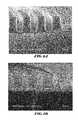
- FIGS. 1A and 1Billustrate a typical example of a silicon nitride film, which could be used in spacer applications.
- the filmwas deposited at 400° C. using a PEALD process other than those described in the present application.
- FIG. 1Aillustrates the film after it was deposited on a three-dimensional surface but prior to being etched by HF. An etching process was then performed by dipping the workpiece in 0.5% HF for about 60 seconds.
- FIG. 1Billustrates the extent to which vertical portions of the silicon nitride film etch to a greater extent than the horizontal portions of the film. The film thicknesses are indicated in nanometers. Structures such as these would not generally survive further processing, such as in a FinFET spacer application.
- atomic layer deposition (ALD) methods of forming silicon nitride filmsare provided.
- the ALD methodsmay be plasma enhanced ALD methods or thermal ALD methods.
- the methodsallow for the deposition of silicon nitride films with desirable qualities, such as good step coverage and pattern loading effects, as well as desirable etch characteristics.
- the silicon nitride filmshave a relatively uniform etch rate for both the vertical and the horizontal portions, when deposited onto 3-dimensional structures.
- Such three-dimensional structuresmay include, for example and without limitation, FinFETS or other types of multiple gate FETs.
- various silicon nitride films of the present disclosurehave an etch rate of less than half the thermal oxide removal rate of about 2-3 nm per minute with diluted HF (0.5%).
- methods of depositing silicon nitride films on substrate in a reaction chambercomprise introducing a vapor phase silicon reactant to the reaction space such that the silicon precursor adsorbs on the substrate surface, removing excess silicon reactant, contacting the adsorbed silicon reactant with a reactive species generated by plasma from a nitrogen precursor, and removing excess reactive species and reaction by-products. These steps are repeated to achieve a silicon nitride film of the desired thickness.
- the silicon precursorcomprises a precursor of formulas (1)-(8) as described herein.
- the silicon precursoris selected from the group consisting of HSiI 3 , H 2 SiI 2 , H 3 SiI, H 2 Si 2 I 4 , H 4 Si 2 I 2 , and H 5 Si 2 I.
- the silicon precursoris H 2 SiI 2 .
- the reactive speciesmay comprise, for example, hydrogen, hydrogen atoms, hydrogen plasma, hydrogen radicals, N*, NH* or NH 2 * radicals.
- the silicon nitride filmis deposited on a three-dimensional structure. In some embodiments the silicon nitride film exhibits a step coverage and pattern loading effect of at least about 80%. In some embodiments the structure comprises a sidewall and top regions and the sidewall wet etch rate (WER) of the silicon nitride film relative to the top region WER is less than about 3 in 0.5% dHF. In some embodiments the etch rate of the silicon nitride film is less than about 0.4 nm/min in 0.5% aqueous HF.
- WERsidewall wet etch rate
- methods of depositing a silicon nitride filmcomprise loading a substrate comprising at least one three-dimensional feature into a reaction space, introducing a silicon precursor into the reaction space so that the silicon precursor is adsorbed on a surface of the substrate, purging the reaction space of excess silicon precursor, introducing a nitrogen precursor into the reaction space, purging the reaction space of excess nitrogen precursor, and repeating the steps to produce a film of the desired thickness.
- the filmhas a step coverage of more than about 50% on the three-dimensional feature.
- the wet etch rate of the silicon nitride filmis less than about 5 nm/min in 5% aqueous HF.
- a ratio of an etch rate of the silicon nitride film in a sidewall of a three-dimensional structure to an etch rate on a top surfaceis less than about 4. In some embodiments the step coverage is at least about 80% or 90%.
- methods of depositing a silicon nitride film on a substratecomprise, exposing the substrate to a vapor phase silicon precursor so that the silicon precursor is adsorbed on a surface of the substrate, exposing the substrate to a purge gas and/or a vacuum to remove excess precursor and reaction byproducts from the substrate surface, contacting the adsorbed silicon precursor with species generated by a nitrogen plasma, exposing the substrate to a purge gas and/or a vacuum to remove the species of a nitrogen containing plasma and reaction byproducts from the substrate surface and from the proximity of the substrate surface, and repeating the steps to produce a film of the desired thickness.
- methods of depositing a silicon nitride film on a substratecomprise, exposing the substrate to a vapor phase silicon reactant so that the silicon reactant is adsorbed on a surface of the substrate, exposing the substrate to a purge gas and/or a vacuum to remove excess precursor and reaction byproducts from the substrate surface, contacting the adsorbed silicon reactant with a nitrogen precursor, exposing the substrate to a purge gas and/or a vacuum to remove excess nitrogen precursor and reaction byproducts from the substrate surface and from the proximity of the substrate surface, and repeating the steps to produce a film of the desired thickness.
- the silicon precursorcomprises iodine or bromine.
- the filmhas a step coverage of more than about 50%.
- the etch rate of the silicon nitrideis less than about 5 nm/min in 0.5% aqueous HF.
- a ratio of an etch rate of the silicon nitride on a sidewall of a three-dimensional structure to an etch rate on a top surface of the three-dimensional structureis less than about 4.
- FIGS. 1A and 1Billustrate the results of an etching process on a silicon nitride film
- FIG. 2is a flow chart generally illustrating a method of forming a silicon nitride film by an ALD process in accordance with some embodiments of the present disclosure
- FIG. 3is a flow chart illustrating a method of forming a silicon nitride thin film by a PEALD process in accordance with some embodiments of the present disclosure
- FIG. 4is a flow chart illustrating a method of forming a silicon nitride thin film by a thermal ALD process in accordance with some embodiments of the present disclosure
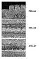
- FIGS. 5A-5Cillustrate field emission scanning electron microscopy (FESEM) images of various silicon nitride films deposited according to some embodiments of the present disclosure.
- FESEMfield emission scanning electron microscopy
- FIGS. 6A-6Cillustrate FESEM images of the silicon nitride films of FIGS. 5A-5B after exposure to a 2-minute dHF dip.
- Silicon nitride filmshave a wide variety of applications, as will be apparent to the skilled artisan, such as in planar logic, DRAM, and NAND Flash devices. More specifically, conformal silicon nitride thin films that display uniform etch behavior have a wide variety of applications, both in the semiconductor industry and also outside of the semiconductor industry. According to some embodiments of the present disclosure, various silicon nitride films and precursors and methods for depositing those films by atomic layer deposition (ALD) are provided. Importantly, in some embodiments the silicon nitride films have a relatively uniform etch rate for both the vertical and the horizontal portions, when deposited onto 3-dimensional structures. Such three-dimensional structures may include, for example and without limitation, FinFETS or other types of multiple gate FETs. In some embodiments, various silicon nitride films of the present disclosure have an etch rate of less than half the thermal oxide removal rate of about 2-3 nm per minute with diluted HF (0.5%).
- Thin film layers comprising silicon nitridecan be deposited by plasma-enhanced atomic layer deposition (PEALD) type processes or by thermal ALD processes.
- PEALDplasma-enhanced atomic layer deposition
- thermal ALDthermal ALD process.
- a silicon nitride thin filmis deposited over a three dimensional structure, such as a fin in the formation of a finFET device.
- the formula of the silicon nitrideis generally referred to herein as SiN for convenience and simplicity.
- the skilled artisanwill understand that the actual formula of the silicon nitride, representing the Si:N ratio in the film and excluding hydrogen or other impurities, can be represented as SiN x , where x varies from about 0.5 to about 2.0, as long as some Si—N bonds are formed. In some cases, x may vary from about 0.9 to about 1.7, from about 1.0 to about 1.5, or from about 1.2 to about 1.4.
- silicon nitrideis formed where Si has an oxidation state of +IV and the amount of nitride in the material might vary.
- ALD-type processesare based on controlled, generally self-limiting surface reactions. Gas phase reactions are typically avoided by contacting the substrate alternately and sequentially with the reactants. Vapor phase reactants are separated from each other in the reaction chamber, for example, by removing excess reactants and/or reactant byproducts between reactant pulses. The reactants may be removed from proximity with the substrate surface with the aid of a purge gas and/or vacuum. In some embodiments excess reactants and/or reactant byproducts are removed from the reaction space by purging, for example with an inert gas.
- ALD-type processesare used to form SiN thin films on substrates such as integrated circuit workpieces, and in some embodiments on three-dimensional structures on the substrates.
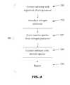
- FIG. 2is a flow chart generally illustrating a silicon nitride ALD deposition cycle that can be used to deposit a silicon nitride thin film in accordance with some embodiments.
- a silicon nitride thin filmis formed on a substrate by an ALD-type process comprising multiple silicon nitride deposition cycles, each silicon nitride deposition cycle 200 comprising:
- Excess reactantsmay be removed from the vicinity of the substrate, for example by purging from the reaction space with an inert gas, after each contacting step.
- an inert gasmay be used to purge from the reaction space with an inert gas.
- PEALDplasma enhanced ALD
- a substrate or workpieceis placed in a reaction chamber and subjected to alternately repeated surface reactions.
- thin SiN filmsare formed by repetition of a self-limiting ALD cycle.
- each ALD cyclecomprises at least two distinct phases.
- the provision and removal of a reactant from the reaction spacemay be considered a phase.
- a first reactant comprising siliconis provided and forms no more than about one monolayer on the substrate surface.
- This reactantis also referred to herein as “the silicon precursor,” “silicon-containing precursor,” or “silicon reactant” and may be, for example, H 2 SiI 2 .
- a second reactantcomprising a reactive species
- the second reactantmay convert adsorbed silicon to silicon nitride.
- the second reactantcomprises a nitrogen precursor.
- the reactive speciescomprises an excited species.
- the second reactantcomprises a species from a nitrogen containing plasma.
- the second reactantcomprises nitrogen radicals, nitrogen atoms and/or nitrogen plasma.
- the second reactantmay comprise other species that are not nitrogen precursors.
- the second reactantmay comprise a plasma of hydrogen, radicals of hydrogen, or atomic hydrogen in one form or another.
- the second reactantmay comprise a species from a noble gas, such as He, Ne, Ar, Kr, or Xe, preferably Ar or He, for example as radicals, in plasma form, or in elemental form.
- a noble gassuch as He, Ne, Ar, Kr, or Xe
- Ar or Hepreferably Ar or He
- radicalsin plasma form, or in elemental form.
- a gas that is used to form a plasmamay flow constantly throughout the deposition process but only be activated intermittently.
- Additional phasesmay be added and phases may be removed as desired to adjust the composition of the final film.
- One or more of the reactantsmay be provided with the aid of a carrier gas, such as Ar or He.
- a carrier gassuch as Ar or He.
- the silicon precursor and the second reactantare provided with the aid of a carrier gas.
- two of the phasesmay overlap, or be combined.
- the silicon precursor and the second reactantmay be provided simultaneously in pulses that partially or completely overlap.
- the order of the phasesmay be varied, and an ALD cycle may begin with any one of the phases. That is, unless specified otherwise, the reactants can be provided in any order, and the process may begin with any of the reactants.
- one or more deposition cyclesbegin with provision of the silicon precursor, followed by the second precursor.
- depositionmay begin with provision of the second precursor, followed by the silicon precursor.
- the substrate on which deposition is desiredis loaded into a reactor.
- the reactormay be part of a cluster tool in which a variety of different processes in the formation of an integrated circuit are carried out.
- a flow-type reactoris utilized.
- a shower head type of reactoris utilized.
- a space divided reactoris utilized.
- a high-volume manufacturing-capable single wafer ALD reactoris used.
- a batch reactorcomprising multiple substrates is used.
- the number of substratesis preferably in the range of 10 to 200, more preferably in the range of 50 to 150, and most preferably in the range of 100 to 130.
- Exemplary single wafer reactorsdesigned specifically to enhance ALD processes, are commercially available from ASM America, Inc. (Phoenix, Ariz.) under the tradenames Pulsar® 2000 and Pulsar® 3000 and ASM Japan K.K (Tokyo, Japan) under the tradename Eagle® XP, XP8 and Dragon®.
- Exemplary batch ALD reactors, designed specifically to enhance ALD processesare commercially available from and ASM Europe B.V (Almere, Netherlands) under the tradenames A400TM and A412TM.
- the exposed surfaces of the workpiececan be pretreated to provide reactive sites to react with the first phase of the ALD process. In some embodiments a separate pretreatment step is not required. In some embodiments the substrate is pretreated to provide a desired surface termination. In some embodiments the substrate is pretreated with plasma.
- reaction chamberis purged between reactant pulses, such as by purging with an inert gas.
- the flow rate and time of each reactantis tunable, as is the removal step, allowing for control of the quality and various properties of the films.
- a gasis provided to the reaction chamber continuously during each deposition cycle, or during the entire ALD process, and reactive species are provided by generating a plasma in the gas, either in the reaction chamber or upstream of the reaction chamber.
- the gascomprises nitrogen.
- the gasis nitrogen.
- the gasmay comprise helium, or argon.
- the gasis helium or nitrogen.
- the flowing gasmay also serve as a purge gas for the first and/or second reactant (or reactive species).
- flowing nitrogenmay serve as a purge gas for a first silicon precursor and also serve as a second reactant (as a source of reactive species).
- nitrogen, argon, or heliummay serve as a purge gas for a first precursor and a source of excited species for converting the silicon precursor to the silicon nitride film.
- the cycleis repeated until a film of the desired thickness and composition is obtained.
- the deposition parameterssuch as the flow rate, flow time, purge time, and/or reactants themselves, may be varied in one or more deposition cycles during the ALD process in order to obtain a film with the desired characteristics.
- hydrogen and/or hydrogen plasmaare not provided in a deposition cycle, or in the deposition process.
- pulsemay be understood to comprise feeding reactant into the reaction chamber for a predetermined amount of time.
- pulsedoes not restrict the length or duration of the pulse and a pulse can be any length of time.
- the silicon reactantis provided first. After an initial surface termination, if necessary or desired, a first silicon reactant pulse is supplied to the workpiece.
- the first reactant pulsecomprises a carrier gas flow and a volatile silicon species, such as H 2 SiI 2 , that is reactive with the workpiece surfaces of interest. Accordingly, the silicon reactant adsorbs upon these workpiece surfaces.
- the first reactant pulseself-saturates the workpiece surfaces such that any excess constituents of the first reactant pulse do not further react with the molecular layer formed by this process.
- the first silicon reactant pulseis preferably supplied in gaseous form.
- the silicon precursor gasis considered “volatile” for purposes of the present description if the species exhibits sufficient vapor pressure under the process conditions to transport the species to the workpiece in sufficient concentration to saturate exposed surfaces.
- the silicon reactant pulseis from about 0.05 seconds to about 5.0 seconds, about 0.1 seconds to about 3 seconds or about 0.2 seconds to about 1.0 seconds.
- the optimum pulsing timecan be readily determined by the skilled artisan based on the particular circumstances.
- excess first silicon reactantis then removed from the reaction space.
- the excess first reactantis purged by stopping the flow of the first chemistry while continuing to flow a carrier gas or purge gas for a sufficient time to diffuse or purge excess reactants and reactant by-products, if any, from the reaction space.
- the excess first precursoris purged with the aid of inert gas, such as nitrogen or argon, that is flowing throughout the ALD cycle.
- the first reactantis purged for about 0.1 seconds to about 10 seconds, about 0.3 seconds to about 5 seconds or about 0.3 seconds to about 1 second. Provision and removal of the silicon reactant can be considered the first or silicon phase of the ALD cycle.
- a second reactant comprising a reactive speciessuch as nitrogen plasma is provided to the workpiece.
- Nitrogen, N 2is flowed continuously to the reaction chamber during each ALD cycle in some embodiments.
- Nitrogen plasmamay be formed by generating a plasma in nitrogen in the reaction chamber or upstream of the reaction chamber, for example by flowing the nitrogen through a remote plasma generator.
- plasmais generated in flowing H 2 and N 2 gases.
- the H 2 and N 2are provided to the reaction chamber before the plasma is ignited or nitrogen and hydrogen atoms or radicals are formed.
- the hydrogenmay have a beneficial effect on the ligand removal step i.e. it may remove some of the remaining ligands or have other beneficial effects on the film quality.
- the H 2 and N 2are provided to the reaction chamber continuously and nitrogen and hydrogen containing plasma, atoms or radicals is created or supplied when needed.
- the second reactantfor example comprising nitrogen plasma
- the second reactantis provided for about 0.1 seconds to about 10 seconds.
- the second reactantsuch as nitrogen plasma
- the second reactant pulsing timemay be even higher than about 10 seconds.
- pulsing timescan be on the order of minutes. The optimum pulsing time can be readily determined by the skilled artisan based on the particular circumstances.
- the second reactantis provided in two or more distinct pulses, without introducing another reactant in between any of the two or more pulses.
- a nitrogen plasmais provided in two or more, preferably in two, sequential pulses, without introducing a Si-precursor in between the sequential pulses.
- two or more sequential plasma pulsesare generated by providing a plasma discharge for a first period of time, extinguishing the plasma discharge for a second period of time, for example from about 0.1 seconds to about 10 seconds, from about 0.5 seconds to about 5 seconds or about 1.0 seconds to about 4.0 seconds, and exciting it again for a third period of time before introduction of another precursor or a removal step, such as before the Si-precursor or a purge step. Additional pulses of plasma can be introduced in the same way.
- a plasmais ignited for an equivalent period of time in each of the pulses.
- Nitrogen plasmamay be generated by applying RF power of from about 10 W to about 2000 W, preferably from about 50 W to about 1000 W, more preferably from about 100 W to about 500 W in some embodiments.
- the RF power densitymay be from about 0.02 W/cm 2 to about 2.0 W/cm 2 , preferably from about 0.05 W/cm 2 to about 1.5 W/cm 2 .
- the RF powermay be applied to nitrogen that flows during the nitrogen plasma pulse time, that flows continuously through the reaction chamber, and/or that flows through a remote plasma generator.
- the plasmais generated in situ, while in other embodiments the plasma is generated remotely.
- any excess reactant and reaction byproductsare removed from the reaction space.
- this stepmay comprise stopping the generation of reactive species and continuing to flow the inert gas, such as nitrogen or argon for a time period sufficient for excess reactive species and volatile reaction by-products to diffuse out of and be purged from the reaction space.
- a separate purge gasmay be used.
- the purgemay, in some embodiments, be from about 0.1 seconds to about 10 seconds, about 0.1 seconds to about 4 seconds or about 0.1 seconds to about 0.5 seconds.
- the nitrogen plasma provision and removalrepresent a second, reactive species phase in a silicon nitride atomic layer deposition cycle.
- the first precursor phasegenerally reacts with the termination left by the last phase in the previous cycle.
- the reactive species phaseis the first phase in the first ALD cycle, in subsequent cycles the reactive species phase will effectively follow the silicon phase.
- one or more different ALD cyclesare provided in the deposition process.
- PEALD reactionsmay be performed at temperatures ranging from about 25° C. to about 700° C., preferably from about 50° C. to about 600° C., more preferably from about 100° C. to about 450° C., and most preferably from about 200° C. to about 400° C.
- the optimum reactor temperaturemay be limited by the maximum allowed thermal budget. Therefore, in some embodiments the reaction temperature is from about 300° C. to about 400° C. In some applications, the maximum temperature is around about 400° C., and, therefore the PEALD process is run at that reaction temperature.
- the pressure of the reaction chamber during processingis maintained at from about 0.01 torr to about 50 torr, preferably from about 0.1 torr to about 10 torr.
- a number of suitable silicon precursorscan be used in the presently disclosed PEALD processes. At least some of the suitable precursors may have the following general formula:
- silicon precursorsmay comprise one or more cyclic compounds.
- Such precursorsmay have the following general formula:
- silicon precursorsmay comprise one or more iodosilanes.
- Such precursorsmay have the following general formula:
- some silicon precursorsmay comprise one or more cyclic iodosilanes.
- Such precursorsmay have the following general formula:
- some silicon precursorsmay comprise one or more bromosilanes.
- Such precursorsmay have the following general formula:
- some silicon precursorsmay comprise one or more cyclic bromosilanes.
- Such precursorsmay have the following general formula:
- preferred silicon precursorscomprise one or more iodosilanes.
- Such precursorsmay have the following general formula:
- preferred silicon precursorscomprise one or more bromosilanes.
- Such precursorsmay have the following general formula:
- suitable silicon precursorscan include at least compounds having any one of the general formulas (1) through (8).
- halides/halogenscan include F, Cl, Br and I.
- a silicon precursorcomprises SiI 4 , HSiI 3 , H 2 SiI 2 , H 3 SiI, Si 2 I 6 , HSi 2 I 5 , H 2 Si 2 I 4 , H 3 Si 2 I 3 , H 4 Si 2 I 2 , H 5 Si 2 I, or Si 3 I 8 .
- a silicon precursorcomprises one of HSiI 3 , H 2 SiI 2 , H 3 SiI, H 2 Si 2 I 4 , H 4 Si 2 I 2 , and H 5 Si 2 I.
- the silicon precursorcomprises two, three, four, five or six of HSiI 3 , H 2 SiI 2 , H 3 SiI, H 2 Si 2 I 4 , H 4 Si 2 I 2 , and H 5 Si 2 I, including any combinations thereof.
- the Si precursoris H 2 SiI 2 .
- Si precursors of formulas (9)-(16), belowcan be used in PEALD processes.
- the second reactant in a PEALD processmay comprise a nitrogen precursor, which may comprise a reactive species.
- Suitable plasma compositionsinclude nitrogen plasma, radicals of nitrogen, or atomic nitrogen in one form or another.
- hydrogen plasma, radicals of hydrogen, or atomic hydrogen in one form or anotherare also provided.
- a plasmamay also contain noble gases, such as He, Ne, Ar, Kr and Xe, preferably Ar or He, in plasma form, as radicals, or in atomic form.
- the second reactantmay comprise plasma formed from compounds having both N and H, such as NH 3 and N 2 H 4 , a mixture of N 2 /H 2 or other precursors having an N—H bond.
- the second reactantmay be formed, at least in part, from N 2 .
- the second reactantmay be formed, at least in part, from N 2 and H 2 , where the N 2 and H 2 are provided at a flow ratio (N 2 /H 2 ) from about 20:1 to about 1:20, preferably from about 10:1 to about 1:10, more preferably from about 5:1 to about 1:5 and most preferably from about 1:2 to about 4:1, and in some cases 1:1.
- the second reactantmay be formed in some embodiments remotely via plasma discharge (“remote plasma”) away from the substrate or reaction space. In some embodiments, the second reactant may be formed in the vicinity of the substrate or directly above substrate (“direct plasma”).
- FIG. 3is a flow chart generally illustrating a silicon nitride PEALD deposition cycle that can be used to deposit a silicon nitride thin film in accordance with some embodiments.
- a silicon nitride thin filmis formed on a substrate by a PEALD-type process comprising multiple silicon nitride deposition cycles, each silicon nitride deposition cycle 300 comprising:
- Nitrogenmay flow continuously throughout the cycle, with nitrogen plasma formed at the appropriate times to convert adsorbed silicon compound into silicon nitride.
- the substratemay be contacted simultaneously with the silicon compound and the reactive species, while in other embodiments these reactants are provided separately.
- the contacting stepsare repeated 350 until a thin film of a desired thickness and composition is obtained. Excess reactants may be purged from the reaction space after each contacting step, i.e., steps 310 and 340 .
- a silicon nitride thin filmis deposited using a PEALD process on a substrate having three-dimensional features, such as in a FinFET application.
- the processmay comprise the following steps:
- a substrate comprising a three-dimensional structureis provided in a reaction space;
- a silicon-containing precursorsuch as SiI 2 H 2
- SiI 2 H 2a silicon-containing precursor
- a nitrogen-containing precursorsuch as N 2 , NH 3 , N 2 H 4 , or N 2 and H 2 , is introduced into the reaction space;
- Steps (2) through (7)may be repeated until a silicon nitride film of a desired thickness is formed.
- steps (5) and (6)are replaced by a step in which the nitrogen atoms, plasma or radicals are formed remotely and provided to the reaction space.
- the PEALD processis performed at a temperature between about 200° C. to about 400° C., between about 300° C. and about 400° C., or at about 400° C.
- thermal atomic layer deposition (ALD) type processesare used to form silicon nitride films on substrates such as integrated circuit workpieces.
- each thermal ALD cyclecomprises at least two distinct phases.
- the provision and removal of a reactant from the reaction spacemay be considered a phase.
- a first reactant comprising siliconis provided and forms no more than about one monolayer on the substrate surface.
- This reactantis also referred to herein as “the silicon precursor” or “silicon reactant” and may be, for example, H 2 SiI 2 .
- a second reactant comprising a nitrogen-containing compoundis provided and reacts with the adsorbed silicon precursor to form SiN.
- This second reactantmay also be referred to as a “nitrogen precursor” or “nitrogen reactant.”
- the second reactantmay comprise NH 3 or another suitable nitrogen-containing compound. Additional phases may be added and phases may be removed as desired to adjust the composition of the final film.
- One or more of the reactantsmay be provided with the aid of a carrier gas, such as Ar or He.
- a carrier gassuch as Ar or He.
- the silicon precursor and the nitrogen precursorare provided with the aid of a carrier gas.
- two of the phasesmay overlap, or be combined.
- the silicon precursor and the nitrogen precursormay be provided simultaneously in pulses that partially or completely overlap.
- the order of the phases and the order of provision of reactantsmay be varied, and an ALD cycle may begin with any one of the phases or any of the reactants. That is, unless specified otherwise, the reactants can be provided in any order and the process may begin with any of the reactants.
- one or more deposition cyclestypically begins with provision of the silicon precursor followed by the nitrogen precursor. In some embodiments, one or more deposition cycles begins with provision of the nitrogen precursor followed by the silicon precursor.
- one or more of the reactantsmay be provided with the aid of a carrier gas, such as Ar or He.
- the nitrogen precursoris provided with the aid of a carrier gas.
- the order of the phases and thus the order of provision of the reactantsmay be varied, and an ALD cycle may begin with any one of the phases.
- the substrate on which deposition is desiredis loaded into a reactor.
- the reactormay be part of a cluster tool in which a variety of different processes in the formation of an integrated circuit are carried out.
- a flow-type reactoris utilized.
- a shower head type of reactoris utilized.
- a space divided reactoris utilized.
- a high-volume manufacturing-capable single wafer ALD reactoris used.
- a batch reactorcomprising multiple substrates is used.
- the number of substratesis preferably in the range of 10 to 200, more preferably in the range of 50 to 150, and most preferably in the range of 100 to 130.
- Exemplary single wafer reactorsdesigned specifically to enhance ALD processes, are commercially available from ASM America, Inc. (Phoenix, Ariz.) under the tradenames Pulsar® 2000 and Pulsar® 3000 and ASM Japan K.K (Tokyo, Japan) under the tradename Eagle® XP, XP8 and Dragon®.
- Exemplary batch ALD reactors, designed specifically to enhance ALD processesare commercially available from and ASM Europe B.V (Almere, Netherlands) under the tradenames A400TM and A412TM.
- the exposed surfaces of the workpiececan be pretreated to provide reactive sites to react with the first phase of the ALD process. In some embodiments a separate pretreatment step is not required. In some embodiments the substrate is pretreated to provide a desired surface termination.
- excess reactant and reaction byproductsare removed from the vicinity of the precursor, such as from the substrate surface, between reactant pulses.
- excess reactant and reaction byproductsare removed from the reaction chamber by purging between reactant pulses, for example with an inert gas.
- the flow rate and time of each reactantis tunable, as is the purge step, allowing for control of the quality and properties of the films.
- removing excess reactant and/or reaction byproductscomprises moving the substrate.
- a gasis provided to the reaction chamber continuously during each deposition cycle, or during the entire ALD process.
- the gasmay be nitrogen, helium or argon.
- the ALD cycleis repeated until a film of the desired thickness and composition is obtained.
- the deposition parameterssuch as the flow rate, flow time, purge time, and/or precursors themselves, may be varied in one or more deposition cycles during the ALD process in order to obtain a film with the desired characteristics.
- pulsemay be understood to comprise feeding reactant into the reaction chamber for a predetermined amount of time.
- pulsedoes not restrict the length or duration of the pulse and a pulse can be any length of time.
- the silicon precursoris provided first. After an initial surface termination, if necessary or desired, a first silicon precursor pulse is supplied to the workpiece.
- the first precursor pulsecomprises a carrier gas flow and a volatile silicon species, such as H 2 SiI 2 , that is reactive with the workpiece surfaces of interest. Accordingly, the silicon precursor adsorbs upon the workpiece surfaces.
- the first precursor pulseself-saturates the workpiece surfaces such that any excess constituents of the first precursor pulse do not substantially react further with the molecular layer formed by this process.
- the first silicon precursor pulseis preferably supplied in gaseous form.
- the silicon precursor gasis considered “volatile” for purposes of the present description if the species exhibits sufficient vapor pressure under the process conditions to transport the species to the workpiece in sufficient concentration to saturate exposed surfaces.
- the silicon precursor pulseis from about 0.05 seconds to about 5.0 seconds, about 0.1 seconds to about 3 seconds or about 0.2 seconds to about 1.0 second.
- the silicon precursor pulsescan be substantially longer as can be determined by the skilled artisan given the particular circumstances.
- excess first precursoris then removed from the reaction space.
- the excess first precursoris purged by stopping the flow of the first precursor while continuing to flow a carrier gas or purge gas for a sufficient time to diffuse or purge excess reactants and reactant by-products, if any, from the reaction space.
- the first precursoris purged for about 0.1 seconds to about 10 seconds, about 0.3 seconds to about 5 seconds or about 0.3 seconds to about 1 seconds. Provision and removal of the silicon precursor can be considered the first or silicon phase of the ALD cycle. In batch process the first precursor purge can be substantially longer as can be determined by the skilled artisan given the specific circumstances.
- a second, nitrogen precursoris pulsed into the reaction space to contact the substrate surface.
- the nitrogen precursormay be provided with the aid of a carrier gas.
- the nitrogen precursormay be, for example, NH 3 or N 2 H 4 .
- the nitrogen precursor pulseis also preferably supplied in gaseous form.
- the nitrogen precursoris considered “volatile” for purposes of the present description if the species exhibits sufficient vapor pressure under the process conditions to transport the species to the workpiece in sufficient concentration to saturate exposed surfaces.
- the nitrogen precursor pulseis about 0.05 seconds to about 5.0 seconds, 0.1 seconds to about 3.0 seconds or about 0.2 seconds to about 1.0 second.
- the nitrogen precursor pulsescan be substantially longer as can be determined by the skilled artisan given the specific circumstances.
- the second, nitrogen precursoris then removed from the reaction space.
- the flow of the second nitrogen precursoris stopped while continuing to flow a carrier gas for a sufficient time to diffuse or purge excess reactants and reactant by-products, if any, from the reaction space, preferably with greater than about two reaction chamber volumes of the purge gas, more preferably with greater than about three chamber volumes. Provision and removal of the nitrogen precursor can be considered the second or nitrogen phase of the ALD cycle.
- the nitrogen precursoris purged for about 0.1 seconds to about 10.0 seconds, about 0.3 seconds to about 5.0 seconds or about 0.3 seconds to about 1.0 second.
- the first precursor purgecan be substantially longer as can be determined by the skilled artisan given the specific circumstances.
- the flow rate and time of the nitrogen precursor pulse, as well as the removal or purge step of the nitrogen phase,are tunable to achieve a desired composition in the silicon nitride film.
- the adsorption of the nitrogen precursor on the substrate surfaceis typically self-limiting, due to the limited number of binding sites, pulsing parameters can be adjusted such that less than a monolayer of nitrogen is adsorbed in one or more cycles.
- the first precursor phasegenerally reacts with the termination left by the last phase in the previous cycle.
- one or more different ALD cyclesare provided in the deposition process.
- ALD reactionsmay be performed at temperatures ranging from about 25° C. to about 1000° C., preferably from about 100° C. to about 800° C., more preferably from about 200° C. to about 650° C., and most preferably from about 300° C. to about 500° C.
- the optimum reactor temperaturemay be limited by the maximum allowed thermal budget. Therefore, the reaction temperature can be from about 300° C. to about 400° C. In some applications, the maximum temperature is around about 400° C., and, therefore, the process is run at that reaction temperature.
- a number of suitable silicon precursorsmay be used in the presently disclosed thermal. In some embodiments these precursors may also be used in plasma ALD processes in which a film with a desired quality (at least one of the desired WER, WERR, pattern loading effect or/and step coverage features described below) is deposited.
- some silicon precursorscomprise iodine and the film deposited by using that precursor has at least one desired property, for example at least one of the desired WER, WERR, pattern loading effect or/and step coverage features described below.
- some silicon precursorscomprise bromine and the film deposited by using that precursor have at least one desired property, for example at least one of the desired WER, WERR, pattern loading effect or/and step coverage features described below.
- At least some of the suitable precursorsmay have the following general formula:
- some silicon precursorscomprise one or more cyclic compounds.
- Such precursorsmay have the following general formula:
- some silicon precursorscomprise one or more iodosilanes.
- Such precursorsmay have the following general formula:
- some silicon precursorscomprise one or more cyclic iodosilanes.
- Such precursorsmay have the following general formula:
- some silicon precursorscomprise one or more bromosilanes.
- Such precursorsmay have the following general formula:
- some silicon precursorscomprise one or more cyclic bromosilanes.
- Such precursorsmay have the following general formula:
- some silicon precursorscomprise one or more iodosilanes or bromosilanes in which the iodine or bromine is not bonded to the silicon in the compound. Accordingly some suitable compounds may have iodine/bromine substituted alkyl groups. Such precursors may have the following general formula:
- some silicon precursorscomprise one or more cyclic iodosilanes or bromosilanes. Accordingly some suitable cyclic compounds may have iodine/bromine substituted alkyl groups. Such precursors may have the following general formula:
- suitable silicon precursorscan include at least compounds having any one of the general formulas (9) through (16).
- halides/halogenscan include F, Cl, Br and I.
- a silicon precursorcomprises one or more of the following: SiI 4 , HSiI 3 , H 2 SiI 2 , H 3 SiI, Si 2 I 6 , HSi 2 I 5 , H 2 Si 2 I 4 , H 3 Si 2 I 3 , H 4 Si 2 I 2 , H 5 Si 2 I, Si 3 I 8 , HSi 2 I 5 , H 2 Si 2 I 4 , H 3 Si 2 I 3 , H 4 Si 2 I 2 , H 5 Si 2 I, MeSiI 3 , Me 2 SiI 2 , Me 3 SiI, MeSi 2 I 5 , Me 2 Si 2 I 4 , Me 3 Si 2 I 3 , Me 4 Si 2 I 2 , Me 5 Si 2 I, HMeSiI 2 , HMe 2 SiI, HMeSi 2 I 4 , HMe 2 Si 2 I 3 , HMe 3 Si 2 I 2 , HMe 4 Si 2 I, H 2 MeSiI, H 2 MeSi 2 I 3 , HM
- a silicon precursorcomprises one or more of the following: EtMeSiI 2 , Et 2 MeSiI, EtMe 2 SiI, EtMeSi 2 I 4 , Et 2 MeSi 2 I 3 , EtMe 2 Si 2 I 3 , Et 3 MeSi 2 I 2 , Et 2 Me 2 Si 2 I 2 , EtMe 3 Si 2 I 2 , Et 4 Me 2 Si 2 I, Et 3 Me 2 Si 2 I, Et 2 Me 3 Si 2 I, EtMe 4 Si 2 I, HEtMeSiI, HEtMeSi 2 I 3 , HEt 2 MeSi 2 I 2 HEtMe 2 Si 2 I 2 , HEt 3 MeSi 2 I, HEt 2 Me 2 Si 2 I, HEtMe 3 Si 2 I, H 2 EtMeSi 2 I 2 , H 2 EtMeSi 2 I 2 , H 2 Et 2 MeSi 2 I, H 2 EtMe 2 Si 2 I, H 3 EtMeSi 2 I.
- a silicon precursorcomprises one or more of the following: HSiI 3 , H 2 SiI 2 , H 3 SiI, H 2 Si 2 I 4 , H 4 Si 2 I 2 , H 5 Si 2 I, MeSiI 3 , Me 2 SiI 2 , Me 3 SiI, Me 2 Si 2 I 4 , Me 4 Si 2 I 2 , HMeSiI 2 , H 2 Me 2 Si 2 I 2 , EtSiI 3 , Et 2 SiI 2 , Et 3 SiI, Et 2 Si 2 I 4 , Et 4 Si 2 I 2 , and HEtSiI 2 .
- a silicon precursorcomprises two, three, four, five, six, seven, eight, nine, ten, eleven, twelve, thirteen, fourteen, fifteen, sixteen, seventeen, eighteen, nineteen or more compounds selected from HSiI 3 , H 2 SiI 2 , H 3 SiI, H 2 Si 2 I 4 , H 4 Si 2 I 2 , H 5 Si 2 I, MeSiI 3 , Me 2 SiI 2 , Me 3 SiI, Me 2 Si 2 I 4 , Me 4 Si 2 I 2 , HMeSiI 2 , H 2 Me 2 Si 2 I 2 , EtSiI 3 , Et 2 SiI 2 , Et 3 SiI, Et 2 Si 2 I 4 , Et 4 Si 2 I 2 , and HEtSiI 2 , including any combinations thereof.
- the silicon precursoris H 2 SiI 2 .
- silicon precursors containing nitrogensuch as iodine or bromine substituted silazanes, or sulphur
- silicon precursors containing nitrogensuch as iodine or bromine substituted silazanes, or sulphur
- silicon precursors containing nitrogensuch as iodine or bromine substituted silazanes, may be used in the presently disclosed thermal and plasma ALD processes in which a film with desired quality is to be deposited, for example at least one of the desired WER, WERR, pattern loading effect or/and step coverage features described below.
- iodine or bromine substituted silicon precursorsmay have the following general formula:
- iodine or bromine substituted silazane precursorsmay have the following general formula:
- the silicon precursorcomprises Si-compound, such as heterocyclic Si compound, which comprises I or Br.
- cyclic precursorsmay comprise the following substructure:
- the silicon precursorcomprises substructure according to formula (19) and example of this kind of compounds is for example, iodine or bromine substituted cyclosilazanes, such iodine or bromine substituted cyclotrisilazane.
- the silicon precursorcomprises Si-compound, such as silylamine based compound, which comprises I or Br.
- silylamine based Si-precursorsmay have the following general formula:
- the second reactant or nitrogen precursor in a thermal ALD processmay be NH 3 , N 2 H 4 , or any number of other suitable nitrogen compounds having a N—H bond.
- FIG. 4is a flow chart generally illustrating a silicon nitride thermal ALD deposition cycle that can be used to deposit a silicon nitride thin film in accordance with some embodiments.
- a silicon nitride thin filmis formed on a substrate by an ALD-type process comprising multiple silicon nitride deposition cycles, each silicon nitride deposition cycle 400 comprising:
- the contacting stepsare repeated 450 until a thin film of a desired thickness and composition is obtained.
- the substratemay be contacted simultaneously with the silicon compound and the nitrogen precursor, while in other embodiments these reactants are provided separately.
- a silicon nitride thin filmis deposited using a thermal ALD process on a substrate having three-dimensional features, such as in a FinFET application.
- the processmay comprise the following steps, not necessarily performed in this order:
- a silicon-containing precursorsuch as H 2 SiI 2
- a silicon-containing precursorsuch as H 2 SiI 2
- a nitrogen-containing precursorsuch as NH 3 or N 2 H 4 , is introduced into the reaction space to react with the silicon-containing precursor on the substrate;
- steps (2) through (5)may be repeated until a silicon nitride film of a desired thickness is formed.
- the ALD processis performed at a temperature between about 100° C. to about 800° C. or between about 200° C. and about 600° C. or between about 300° C. to about 500° C. In some applications, the reaction temperature is about 400° C.
- Silicon nitride thin films deposited according to some of the embodiments discussed hereinmay achieve impurity levels or concentrations below about 3 at-%, preferably below about 1 at-%, more preferably below about 0.5 at-%, and most preferably below about 0.1 at-%.
- the total impurity level excluding hydrogenmay be below about 5 at-%, preferably below about 2 at-%, more preferably below about 1 at-%, and most preferably below about 0.2 at-%.
- hydrogen levelsmay be below about 30 at-%, preferably below about 20 at-%, more preferably below about 15 at-%, and most preferably below about 10 at-%.
- the deposited SiN filmsdo not comprise an appreciable amount of carbon.
- a SiN film comprising carbonis deposited.
- an ALD reactionis carried out using a silicon precursor comprising carbon and a thin silicon nitride film comprising carbon is deposited.
- a SiN film comprising carbonis deposited using a precursor comprising an alkyl group or other carbon-containing ligand.
- a silicon precursor of one of formulas (9)-(16) and comprising an alkyl groupis used in a PEALD or thermal ALD process, as described above, to deposit a SiN film comprising carbon.
- Different alkyl groupssuch as Me or Et, or other carbon-containing ligands may produce different carbon concentrations in the films because of different reaction mechanisms.
- different precursorscan be selected to produce different carbon concentration in deposited SiN films.
- the thin SiN film comprising carbonmay be used, for example, as a low-k spacer.
- FIGS. 5A-5Bshow FESEM images of various silicon nitride thin films deposited according to the present disclosure. After the films were deposited, they were HF-dipped for 2 minutes.
- FIGS. 6A-6Cshow the same silicon nitride films after the dHF drip process. Uniform etching can be seen.
- the silicon nitride thin filmsmay exhibit step coverage and pattern loading effects of greater than about 50%, preferably greater than about 80%, more preferably greater than about 90%, and most preferably greater than about 95%. In some cases step coverage and pattern loading effects can be greater than about 98% and in some case about 100% (within the accuracy of the measurement tool or method). These values can be achieved in aspect ratios of more than 2, preferably in aspect ratios more than 3, more preferably in aspect ratios more than 5 and most preferably in aspect ratios more than 8.
- pattern loading effectis used in accordance with its ordinary meaning in this field. While pattern loading effects may be seen with respect to impurity content, density, electrical properties and etch rate, unless indicated otherwise the term pattern loading effect when used herein refers to the variation in film thickness in an area of the substrate where structures are present. Thus, the pattern loading effect can be given as the film thickness in the sidewall or bottom of a feature inside a three-dimensional structure relative to the film thickness on the sidewall or bottom of the three-dimensional structure/feature facing the open field. As used herein, a 100% pattern loading effect (or a ratio of 1) would represent about a completely uniform film property throughout the substrate regardless of features i.e. in other words there is no pattern loading effect (variance in a particular film property, such as thickness, in features vs. open field).
- silicon nitride filmsare deposited to a thicknesses of from about 3 nm to about 50 nm, preferably from about 5 nm to about 30 nm, more preferably from about 5 nm to about 20 nm. These thicknesses can be achieved in feature sizes (width) below about 100 nm, preferably about 50 nm, more preferably below about 30 nm, most preferably below about 20 nm, and in some cases below about 15 nm. According to some embodiments, a SiN film is deposited on a three-dimensional structure and the thickness at a sidewall may be slightly even more than 10 nm.
- silicon nitride films with various wet etch ratesmay be deposited.
- WERwet etch rates
- silicon nitride filmsmay have WER values of less than about 5, preferably less than about 4, more preferably less than about 2, and most preferably less than about 1. In some embodiments it could less than about 0.3.
- the blanket WER in 0.5% dHF (nm/min) relative to the WER of thermal oxidemay be less than about 3, preferably less than about 2, more preferably less than about 1, and most preferably less than about 0.5.
- the sidewall WER of the three dimensional feature, such as fin or trench relative to the top region WER of a three dimensional feature, such as fin or trenchmay be less than about 4, preferably less than about 3, more preferably less than about 2, most preferably about 1.
- top and sidemay not be as critical for some applications, due to the improved film quality and etch characteristics. Nevertheless, in some embodiments, the thickness gradient along the sidewall may be very important to subsequent applications or processes.
- the amount of etching of silicon nitride films according to the present disclosuremay be about one or two times less than amount of etching observed for thermal SiO 2 (TOX) in a 0.5% HF-dip process (for example in a process in which about 2 to about 3 nm TOX is removed, one or two times less SiN is removed when deposited according to the methods disclosed herein).
- the WER of preferred silicon nitride filmsmay be less than that of prior art thermal oxide films.
- the methods and materials described hereincan provide films with increased quality and improved etch properties not only for traditional lateral transistor designs, with horizontal source/drain (S/D) and gate surfaces, but can also provide improved SiN films for use on non-horizontal (e.g., vertical) surfaces, and on complex three-dimensional (3D) structures.
- SiN filmsare deposited by the disclosed methods on a three-dimensional structure during integrated circuit fabrication.
- the three-dimensional transistormay include, for example, double-gate field effect transistors (DG FET), and other types of multiple gate FETs, including FinFETs.
- DG FETdouble-gate field effect transistors
- silicon nitride thin films of the present disclosuremay be useful in nonplanar multiple gate transistors, such as FinFETs, where it may be desirable to form silicide on vertical walls, in addition to the tops of the gate, source, and drain regions.
- 3D structure for which the SiN deposition techniques taught herein are particularly usefulis a 3D elevated source/drain structure, as taught in U.S. Patent Publication No. 2009/0315120 A1 by Shifren et al., the disclosure of which is incorporated herein by reference in its entirety. Shifren et al. teach elevated source/drain structures that include vertical sidewalls.
- a silicon nitride thin filmwas deposited at 400° C. according to the present disclosure by a PEALD process using H 2 SiI 2 as the silane precursor and H 2 +N 2 plasma as the nitrogen precursor.
- This filmexhibited a combination of some of the best qualities of both ALD reaction types: the typical high quality of PEALD SiN films and the isotropic etch behavior of thermal ALD films. While these results are not fully understood, the film properties and etch behavior were nevertheless within the specs for the high quality spacer layer application.
- the step coverage and pattern loading effect on a trench structure with an aspect ratio of 2should be over 95%
- the wet etch rate (WER)should be less than 50% of the WER of thermally oxidized silicon (SiO 2 , TOX)
- the etch rateshould be about the same on horizontal and vertical walls of the trench structure.
- the growth rateshould be over 0.5 nm/min and impurity contents as low as possible.
- the film growth ratewas 0.52 ⁇ /cycle, and the thickness non-uniformity 6.2% (1 ⁇ ).
- the refractive indexwas 2.04 with a non-uniformity of 0.7% (1 ⁇ ).
- the growth rate per minutewas not yet optimized and was 0.13 nm/min.
- the wet etch rate of a planar filmwas 1.13 nm/minute, which is 46.7% of the WER of Tox (2.43 nm/min).
- the film conformalitywas from about 91.0 to about 93.1% and the pattern loading effect from about 95.7 to about 99.3% % as deposited (before etching).
- the conformality valuewas from about 91.5 to about 94.6% and the pattern loading effect from about 97.4 to about 99.5% %.
- the wet etch rate top region of the trenchwas A 4.32 nm/min, B 2.98 nm/min on the trench sidewall and C 3.03 nm/min on trench bottom.
- the field areasshowed D 2.63 nm/min etch rate.
- the ligand removal step of iodine or bromineis completed before the plasma discharge. That can avoid leftover ligands from decomposing and re-entering the film as impurities, and in the case of halides, the formation of plasma activated halides is also avoided.
- the composition of a silicon nitride thin film deposited according to the present disclosurewas analyzed by HFS-RBS. The results are shown in Table 1 below. Additionally, XRR data was obtained of the same film. The thickness of the film was determined to be about 117 nm. The mass density was determined to be 2.63 ( ⁇ 0.1) g/cm 3 . And the surface RMS roughness was determined to be 1.76 ( ⁇ 0.1) nm.
Landscapes
- Engineering & Computer Science (AREA)
- Chemical & Material Sciences (AREA)
- Physics & Mathematics (AREA)
- Condensed Matter Physics & Semiconductors (AREA)
- General Physics & Mathematics (AREA)
- Manufacturing & Machinery (AREA)
- Computer Hardware Design (AREA)
- Microelectronics & Electronic Packaging (AREA)
- Power Engineering (AREA)
- Chemical Kinetics & Catalysis (AREA)
- General Chemical & Material Sciences (AREA)
- Materials Engineering (AREA)
- Mechanical Engineering (AREA)
- Metallurgy (AREA)
- Organic Chemistry (AREA)
- Plasma & Fusion (AREA)
- Inorganic Chemistry (AREA)
- Formation Of Insulating Films (AREA)
- Chemical Vapour Deposition (AREA)
- Insulated Gate Type Field-Effect Transistor (AREA)
- Electromagnetism (AREA)
Abstract
Description
- 1. Field of the Invention
- The present disclosure relates generally to the field of semiconductor device manufacturing and, more particularly, to low temperature deposition of silicon nitride films and precursors for use in deposition of silicon nitride films.
- 2. Description of the Related Art
- Spacers are widely used in semiconductor manufacturing as structures to protect against subsequent processing steps. For example, nitride spacers formed beside gate electrodes can be used as a mask to protect underlying source/drain areas during doping or implanting steps.
- As the physical geometry of semiconductor devices shrinks, the gate electrode spacer becomes smaller and smaller. The spacer width is limited by the nitride thickness that can be deposited conformably over the dense gate electrodes lines. So the nitride spacer etching process is preferred to have a high ratio of spacer width to nitride layer thickness as deposited.
- Current PEALD silicon nitride processes in general suffer from anisotropic etch behavior when deposited on a three-dimensional structure, such as a trench structure. In other words, the film deposited on the sidewalls of a trench or fin or another three dimensional feature display inferior film properties as compared to film on the top region of the feature. The film quality may be sufficient for the target application on the top of the trench, or on planar regions of a structured wafer, but not on the sidewalls or other non-horizontal or vertical surfaces.
FIGS. 1A and 1B illustrate a typical example of a silicon nitride film, which could be used in spacer applications. The film was deposited at 400° C. using a PEALD process other than those described in the present application.FIG. 1A illustrates the film after it was deposited on a three-dimensional surface but prior to being etched by HF. An etching process was then performed by dipping the workpiece in 0.5% HF for about 60 seconds.FIG. 1B illustrates the extent to which vertical portions of the silicon nitride film etch to a greater extent than the horizontal portions of the film. The film thicknesses are indicated in nanometers. Structures such as these would not generally survive further processing, such as in a FinFET spacer application.- In some aspects, atomic layer deposition (ALD) methods of forming silicon nitride films are provided. The ALD methods may be plasma enhanced ALD methods or thermal ALD methods. The methods allow for the deposition of silicon nitride films with desirable qualities, such as good step coverage and pattern loading effects, as well as desirable etch characteristics. According to some embodiments, the silicon nitride films have a relatively uniform etch rate for both the vertical and the horizontal portions, when deposited onto 3-dimensional structures. Such three-dimensional structures may include, for example and without limitation, FinFETS or other types of multiple gate FETs. In some embodiments, various silicon nitride films of the present disclosure have an etch rate of less than half the thermal oxide removal rate of about 2-3 nm per minute with diluted HF (0.5%).
- In some embodiments, methods of depositing silicon nitride films on substrate in a reaction chamber comprise introducing a vapor phase silicon reactant to the reaction space such that the silicon precursor adsorbs on the substrate surface, removing excess silicon reactant, contacting the adsorbed silicon reactant with a reactive species generated by plasma from a nitrogen precursor, and removing excess reactive species and reaction by-products. These steps are repeated to achieve a silicon nitride film of the desired thickness.
- In some embodiments, the silicon precursor comprises a precursor of formulas (1)-(8) as described herein. In some embodiments the silicon precursor is selected from the group consisting of HSiI3, H2SiI2, H3SiI, H2Si2I4, H4Si2I2, and H5Si2I. In some embodiments the silicon precursor is H2SiI2. The reactive species may comprise, for example, hydrogen, hydrogen atoms, hydrogen plasma, hydrogen radicals, N*, NH* or NH2* radicals.
- In some embodiments the silicon nitride film is deposited on a three-dimensional structure. In some embodiments the silicon nitride film exhibits a step coverage and pattern loading effect of at least about 80%. In some embodiments the structure comprises a sidewall and top regions and the sidewall wet etch rate (WER) of the silicon nitride film relative to the top region WER is less than about 3 in 0.5% dHF. In some embodiments the etch rate of the silicon nitride film is less than about 0.4 nm/min in 0.5% aqueous HF.
- In some embodiments, methods of depositing a silicon nitride film comprise loading a substrate comprising at least one three-dimensional feature into a reaction space, introducing a silicon precursor into the reaction space so that the silicon precursor is adsorbed on a surface of the substrate, purging the reaction space of excess silicon precursor, introducing a nitrogen precursor into the reaction space, purging the reaction space of excess nitrogen precursor, and repeating the steps to produce a film of the desired thickness. In some embodiments the film has a step coverage of more than about 50% on the three-dimensional feature. In some embodiments the wet etch rate of the silicon nitride film is less than about 5 nm/min in 5% aqueous HF. In some embodiments a ratio of an etch rate of the silicon nitride film in a sidewall of a three-dimensional structure to an etch rate on a top surface is less than about 4. In some embodiments the step coverage is at least about 80% or 90%.
- In some embodiments, methods of depositing a silicon nitride film on a substrate comprise, exposing the substrate to a vapor phase silicon precursor so that the silicon precursor is adsorbed on a surface of the substrate, exposing the substrate to a purge gas and/or a vacuum to remove excess precursor and reaction byproducts from the substrate surface, contacting the adsorbed silicon precursor with species generated by a nitrogen plasma, exposing the substrate to a purge gas and/or a vacuum to remove the species of a nitrogen containing plasma and reaction byproducts from the substrate surface and from the proximity of the substrate surface, and repeating the steps to produce a film of the desired thickness.
- In some embodiments, methods of depositing a silicon nitride film on a substrate comprise, exposing the substrate to a vapor phase silicon reactant so that the silicon reactant is adsorbed on a surface of the substrate, exposing the substrate to a purge gas and/or a vacuum to remove excess precursor and reaction byproducts from the substrate surface, contacting the adsorbed silicon reactant with a nitrogen precursor, exposing the substrate to a purge gas and/or a vacuum to remove excess nitrogen precursor and reaction byproducts from the substrate surface and from the proximity of the substrate surface, and repeating the steps to produce a film of the desired thickness.
- In some embodiments the silicon precursor comprises iodine or bromine. In some embodiments the film has a step coverage of more than about 50%. In some embodiments the etch rate of the silicon nitride is less than about 5 nm/min in 0.5% aqueous HF. In some embodiments a ratio of an etch rate of the silicon nitride on a sidewall of a three-dimensional structure to an etch rate on a top surface of the three-dimensional structure is less than about 4.
- The invention will be better understood from the Detailed Description of the Preferred Embodiments and from the appended drawings, which are meant to illustrate and not to limit the invention, and wherein:
FIGS. 1A and 1B illustrate the results of an etching process on a silicon nitride film;FIG. 2 is a flow chart generally illustrating a method of forming a silicon nitride film by an ALD process in accordance with some embodiments of the present disclosure;FIG. 3 is a flow chart illustrating a method of forming a silicon nitride thin film by a PEALD process in accordance with some embodiments of the present disclosure;FIG. 4 is a flow chart illustrating a method of forming a silicon nitride thin film by a thermal ALD process in accordance with some embodiments of the present disclosure;FIGS. 5A-5C illustrate field emission scanning electron microscopy (FESEM) images of various silicon nitride films deposited according to some embodiments of the present disclosure.FIGS. 6A-6C illustrate FESEM images of the silicon nitride films ofFIGS. 5A-5B after exposure to a 2-minute dHF dip.- Silicon nitride films have a wide variety of applications, as will be apparent to the skilled artisan, such as in planar logic, DRAM, and NAND Flash devices. More specifically, conformal silicon nitride thin films that display uniform etch behavior have a wide variety of applications, both in the semiconductor industry and also outside of the semiconductor industry. According to some embodiments of the present disclosure, various silicon nitride films and precursors and methods for depositing those films by atomic layer deposition (ALD) are provided. Importantly, in some embodiments the silicon nitride films have a relatively uniform etch rate for both the vertical and the horizontal portions, when deposited onto 3-dimensional structures. Such three-dimensional structures may include, for example and without limitation, FinFETS or other types of multiple gate FETs. In some embodiments, various silicon nitride films of the present disclosure have an etch rate of less than half the thermal oxide removal rate of about 2-3 nm per minute with diluted HF (0.5%).
- Thin film layers comprising silicon nitride can be deposited by plasma-enhanced atomic layer deposition (PEALD) type processes or by thermal ALD processes. In some embodiments, silicon nitride thin films are deposited on a substrate by PEALD. In some embodiments, silicon nitride thin films are deposited on a substrate by a thermal ALD process. In some embodiments a silicon nitride thin film is deposited over a three dimensional structure, such as a fin in the formation of a finFET device.
- The formula of the silicon nitride is generally referred to herein as SiN for convenience and simplicity. However, the skilled artisan will understand that the actual formula of the silicon nitride, representing the Si:N ratio in the film and excluding hydrogen or other impurities, can be represented as SiNx, where x varies from about 0.5 to about 2.0, as long as some Si—N bonds are formed. In some cases, x may vary from about 0.9 to about 1.7, from about 1.0 to about 1.5, or from about 1.2 to about 1.4. In some embodiments silicon nitride is formed where Si has an oxidation state of +IV and the amount of nitride in the material might vary.
- ALD-type processes are based on controlled, generally self-limiting surface reactions. Gas phase reactions are typically avoided by contacting the substrate alternately and sequentially with the reactants. Vapor phase reactants are separated from each other in the reaction chamber, for example, by removing excess reactants and/or reactant byproducts between reactant pulses. The reactants may be removed from proximity with the substrate surface with the aid of a purge gas and/or vacuum. In some embodiments excess reactants and/or reactant byproducts are removed from the reaction space by purging, for example with an inert gas.
- The methods presented herein provide for deposition of SiN thin films on substrate surfaces. Geometrically challenging applications are also possible due to the nature of ALD-type processes. According to some embodiments, ALD-type processes are used to form SiN thin films on substrates such as integrated circuit workpieces, and in some embodiments on three-dimensional structures on the substrates.
FIG. 2 is a flow chart generally illustrating a silicon nitride ALD deposition cycle that can be used to deposit a silicon nitride thin film in accordance with some embodiments. According to certain embodiments, a silicon nitride thin film is formed on a substrate by an ALD-type process comprising multiple silicon nitride deposition cycles, each siliconnitride deposition cycle 200 comprising:- (1) contacting a substrate with a
silicon precursor 210 such that the silicon precursor adsorbs on the substrate surface; - (2) contacting the substrate with a
nitrogen precursor 220; and - (3) repeating
steps - Excess reactants may be removed from the vicinity of the substrate, for example by purging from the reaction space with an inert gas, after each contacting step. The discussion below addresses each of these steps in greater detail.
- In some embodiments, plasma enhanced ALD (PEALD) processes are used to deposit SiN films. Briefly, a substrate or workpiece is placed in a reaction chamber and subjected to alternately repeated surface reactions. In some embodiments, thin SiN films are formed by repetition of a self-limiting ALD cycle. Preferably, for forming SiN films, each ALD cycle comprises at least two distinct phases. The provision and removal of a reactant from the reaction space may be considered a phase. In a first phase, a first reactant comprising silicon is provided and forms no more than about one monolayer on the substrate surface. This reactant is also referred to herein as “the silicon precursor,” “silicon-containing precursor,” or “silicon reactant” and may be, for example, H2SiI2.
- In a second phase, a second reactant comprising a reactive species is provided and may convert adsorbed silicon to silicon nitride. In some embodiments the second reactant comprises a nitrogen precursor. In some embodiments, the reactive species comprises an excited species. In some embodiments the second reactant comprises a species from a nitrogen containing plasma. In some embodiments, the second reactant comprises nitrogen radicals, nitrogen atoms and/or nitrogen plasma. The second reactant may comprise other species that are not nitrogen precursors. In some embodiments, the second reactant may comprise a plasma of hydrogen, radicals of hydrogen, or atomic hydrogen in one form or another. In some embodiments, the second reactant may comprise a species from a noble gas, such as He, Ne, Ar, Kr, or Xe, preferably Ar or He, for example as radicals, in plasma form, or in elemental form. These reactive species from noble gases do not necessarily contribute material to the deposited film, but can in some circumstances contribute to film growth as well as help in the formation and ignition of plasma. In some embodiments a gas that is used to form a plasma may flow constantly throughout the deposition process but only be activated intermittently.
- Additional phases may be added and phases may be removed as desired to adjust the composition of the final film.
- One or more of the reactants may be provided with the aid of a carrier gas, such as Ar or He. In some embodiments the silicon precursor and the second reactant are provided with the aid of a carrier gas.
- In some embodiments, two of the phases may overlap, or be combined. For example, the silicon precursor and the second reactant may be provided simultaneously in pulses that partially or completely overlap. In addition, although referred to as the first and second phases, and the first and second reactants, the order of the phases may be varied, and an ALD cycle may begin with any one of the phases. That is, unless specified otherwise, the reactants can be provided in any order, and the process may begin with any of the reactants.
- As discussed in more detail below, in some embodiments for depositing a silicon nitride film, one or more deposition cycles begin with provision of the silicon precursor, followed by the second precursor. In other embodiments deposition may begin with provision of the second precursor, followed by the silicon precursor.
- In some embodiments the substrate on which deposition is desired, such as a semiconductor workpiece, is loaded into a reactor. The reactor may be part of a cluster tool in which a variety of different processes in the formation of an integrated circuit are carried out. In some embodiments a flow-type reactor is utilized. In some embodiments a shower head type of reactor is utilized. In some embodiment, a space divided reactor is utilized. In some embodiments a high-volume manufacturing-capable single wafer ALD reactor is used. In other embodiments a batch reactor comprising multiple substrates is used. For embodiments in which batch ALD reactors are used, the number of substrates is preferably in the range of 10 to 200, more preferably in the range of 50 to 150, and most preferably in the range of 100 to 130.
- Exemplary single wafer reactors, designed specifically to enhance ALD processes, are commercially available from ASM America, Inc. (Phoenix, Ariz.) under the tradenames Pulsar® 2000 and Pulsar® 3000 and ASM Japan K.K (Tokyo, Japan) under the tradename Eagle® XP, XP8 and Dragon®. Exemplary batch ALD reactors, designed specifically to enhance ALD processes, are commercially available from and ASM Europe B.V (Almere, Netherlands) under the tradenames A400™ and A412™.
- In some embodiments, if necessary, the exposed surfaces of the workpiece can be pretreated to provide reactive sites to react with the first phase of the ALD process. In some embodiments a separate pretreatment step is not required. In some embodiments the substrate is pretreated to provide a desired surface termination. In some embodiments the substrate is pretreated with plasma.
- Excess reactant and reaction byproducts, if any, are removed from the vicinity of the substrate, and in particular from the substrate surface, between reactant pulses. In some embodiments the reaction chamber is purged between reactant pulses, such as by purging with an inert gas. The flow rate and time of each reactant, is tunable, as is the removal step, allowing for control of the quality and various properties of the films.
- As mentioned above, in some embodiments a gas is provided to the reaction chamber continuously during each deposition cycle, or during the entire ALD process, and reactive species are provided by generating a plasma in the gas, either in the reaction chamber or upstream of the reaction chamber. In some embodiments the gas comprises nitrogen. In some embodiments the gas is nitrogen. In other embodiments the gas may comprise helium, or argon. In some embodiments the gas is helium or nitrogen. The flowing gas may also serve as a purge gas for the first and/or second reactant (or reactive species). For example, flowing nitrogen may serve as a purge gas for a first silicon precursor and also serve as a second reactant (as a source of reactive species). In some embodiments, nitrogen, argon, or helium may serve as a purge gas for a first precursor and a source of excited species for converting the silicon precursor to the silicon nitride film.
- The cycle is repeated until a film of the desired thickness and composition is obtained. In some embodiments the deposition parameters, such as the flow rate, flow time, purge time, and/or reactants themselves, may be varied in one or more deposition cycles during the ALD process in order to obtain a film with the desired characteristics. In some embodiments, hydrogen and/or hydrogen plasma are not provided in a deposition cycle, or in the deposition process.
- The term “pulse” may be understood to comprise feeding reactant into the reaction chamber for a predetermined amount of time. The term “pulse” does not restrict the length or duration of the pulse and a pulse can be any length of time.
- In some embodiments, the silicon reactant is provided first. After an initial surface termination, if necessary or desired, a first silicon reactant pulse is supplied to the workpiece. In accordance with some embodiments, the first reactant pulse comprises a carrier gas flow and a volatile silicon species, such as H2SiI2, that is reactive with the workpiece surfaces of interest. Accordingly, the silicon reactant adsorbs upon these workpiece surfaces. The first reactant pulse self-saturates the workpiece surfaces such that any excess constituents of the first reactant pulse do not further react with the molecular layer formed by this process.
- The first silicon reactant pulse is preferably supplied in gaseous form. The silicon precursor gas is considered “volatile” for purposes of the present description if the species exhibits sufficient vapor pressure under the process conditions to transport the species to the workpiece in sufficient concentration to saturate exposed surfaces.
- In some embodiments the silicon reactant pulse is from about 0.05 seconds to about 5.0 seconds, about 0.1 seconds to about 3 seconds or about 0.2 seconds to about 1.0 seconds. The optimum pulsing time can be readily determined by the skilled artisan based on the particular circumstances.
- After sufficient time for a molecular layer to adsorb on the substrate surface, excess first silicon reactant is then removed from the reaction space. In some embodiments the excess first reactant is purged by stopping the flow of the first chemistry while continuing to flow a carrier gas or purge gas for a sufficient time to diffuse or purge excess reactants and reactant by-products, if any, from the reaction space. In some embodiments the excess first precursor is purged with the aid of inert gas, such as nitrogen or argon, that is flowing throughout the ALD cycle.
- In some embodiments, the first reactant is purged for about 0.1 seconds to about 10 seconds, about 0.3 seconds to about 5 seconds or about 0.3 seconds to about 1 second. Provision and removal of the silicon reactant can be considered the first or silicon phase of the ALD cycle.
- In the second phase, a second reactant comprising a reactive species, such as nitrogen plasma is provided to the workpiece. Nitrogen, N2, is flowed continuously to the reaction chamber during each ALD cycle in some embodiments. Nitrogen plasma may be formed by generating a plasma in nitrogen in the reaction chamber or upstream of the reaction chamber, for example by flowing the nitrogen through a remote plasma generator.
- In some embodiments, plasma is generated in flowing H2and N2gases. In some embodiments the H2and N2are provided to the reaction chamber before the plasma is ignited or nitrogen and hydrogen atoms or radicals are formed. Without being bound to any theory, it is believed that the hydrogen may have a beneficial effect on the ligand removal step i.e. it may remove some of the remaining ligands or have other beneficial effects on the film quality. In some embodiments the H2and N2are provided to the reaction chamber continuously and nitrogen and hydrogen containing plasma, atoms or radicals is created or supplied when needed.
- Typically, the second reactant, for example comprising nitrogen plasma, is provided for about 0.1 seconds to about 10 seconds. In some embodiments the second reactant, such as nitrogen plasma, is provided for about 0.1 seconds to about 10 seconds, 0.5 seconds to about 5 seconds or 0.5 seconds to about 2.0 seconds. However, depending on the reactor type, substrate type and its surface area, the second reactant pulsing time may be even higher than about 10 seconds. In some embodiments, pulsing times can be on the order of minutes. The optimum pulsing time can be readily determined by the skilled artisan based on the particular circumstances.
- In some embodiments the second reactant is provided in two or more distinct pulses, without introducing another reactant in between any of the two or more pulses. For example, in some embodiments a nitrogen plasma is provided in two or more, preferably in two, sequential pulses, without introducing a Si-precursor in between the sequential pulses. In some embodiments during provision of nitrogen plasma two or more sequential plasma pulses are generated by providing a plasma discharge for a first period of time, extinguishing the plasma discharge for a second period of time, for example from about 0.1 seconds to about 10 seconds, from about 0.5 seconds to about 5 seconds or about 1.0 seconds to about 4.0 seconds, and exciting it again for a third period of time before introduction of another precursor or a removal step, such as before the Si-precursor or a purge step. Additional pulses of plasma can be introduced in the same way. In some embodiments a plasma is ignited for an equivalent period of time in each of the pulses.
- Nitrogen plasma may be generated by applying RF power of from about 10 W to about 2000 W, preferably from about 50 W to about 1000 W, more preferably from about 100 W to about 500 W in some embodiments. In some embodiments the RF power density may be from about 0.02 W/cm2to about 2.0 W/cm2, preferably from about 0.05 W/cm2to about 1.5 W/cm2. The RF power may be applied to nitrogen that flows during the nitrogen plasma pulse time, that flows continuously through the reaction chamber, and/or that flows through a remote plasma generator. Thus in some embodiments the plasma is generated in situ, while in other embodiments the plasma is generated remotely.
- After a time period sufficient to completely saturate and react the previously adsorbed molecular layer with the nitrogen plasma pulse, any excess reactant and reaction byproducts are removed from the reaction space. As with the removal of the first\reactant, this step may comprise stopping the generation of reactive species and continuing to flow the inert gas, such as nitrogen or argon for a time period sufficient for excess reactive species and volatile reaction by-products to diffuse out of and be purged from the reaction space. In other embodiments a separate purge gas may be used. The purge may, in some embodiments, be from about 0.1 seconds to about 10 seconds, about 0.1 seconds to about 4 seconds or about 0.1 seconds to about 0.5 seconds. Together, the nitrogen plasma provision and removal represent a second, reactive species phase in a silicon nitride atomic layer deposition cycle.
- The two phases together represent one ALD cycle, which is repeated to form silicon nitride thin films of a desired thickness. While the ALD cycle is generally referred to herein as beginning with the silicon phase, it is contemplated that in other embodiments the cycle may begin with the reactive species phase. One of skill in the art will recognize that the first precursor phase generally reacts with the termination left by the last phase in the previous cycle. Thus, while no reactant may be previously adsorbed on the substrate surface or present in the reaction space if the reactive species phase is the first phase in the first ALD cycle, in subsequent cycles the reactive species phase will effectively follow the silicon phase. In some embodiments one or more different ALD cycles are provided in the deposition process.
- According to some embodiments of the present disclosure, PEALD reactions may be performed at temperatures ranging from about 25° C. to about 700° C., preferably from about 50° C. to about 600° C., more preferably from about 100° C. to about 450° C., and most preferably from about 200° C. to about 400° C. In some embodiments, the optimum reactor temperature may be limited by the maximum allowed thermal budget. Therefore, in some embodiments the reaction temperature is from about 300° C. to about 400° C. In some applications, the maximum temperature is around about 400° C., and, therefore the PEALD process is run at that reaction temperature.
- According to some embodiments of the present disclosure, the pressure of the reaction chamber during processing is maintained at from about 0.01 torr to about 50 torr, preferably from about 0.1 torr to about 10 torr.
- A number of suitable silicon precursors can be used in the presently disclosed PEALD processes. At least some of the suitable precursors may have the following general formula:
H2n+2−y−zSinXyAz (1)- wherein, n=1-10, y=1 or more (and up to 2n+2−z), z=0 or more (and up to 2n+2−y), X is I or Br, and A is a halogen other than X, preferably n=1-5 and more preferably n=1-3 and most preferably 1-2.
- According to some embodiments, silicon precursors may comprise one or more cyclic compounds. Such precursors may have the following general formula:
H2n−y−zSinXyAz (2)- wherein the formula (2) compound is cyclic compound, n=3-10, y=1 or more (and up to 2n−z), z=0 or more (and up to 2n−y), X is I or Br, and A is a halogen other than X, preferably n=3-6.
- According to some embodiments, silicon precursors may comprise one or more iodosilanes. Such precursors may have the following general formula:
H2n+2−y−zSinIyAz (3)- wherein, n=1-10, y=1 or more (and up to 2n+2−z), z=0 or more (and up to 2n+2−y), and A is a halogen other than I, preferably n=1-5 and more preferably n=1-3 and most preferably 1-2.
- According to some embodiments, some silicon precursors may comprise one or more cyclic iodosilanes. Such precursors may have the following general formula:
H2n−y−zSinIyAz (4)- wherein the formula (4) compound is a cyclic compound, n=3-10, y=1 or more (and up to 2n−z), z=0 or more (and up to 2n−y), and A is a halogen other than I, preferably n=3-6.
- According to some embodiments, some silicon precursors may comprise one or more bromosilanes. Such precursors may have the following general formula:
H2n+2−y−zSinBryAz (5)- wherein, n=1-10, y=1 or more (and up to 2n+2−z), z=0 or more (and up to 2n+2−y), and A is a halogen other than Br, preferably n=1-5 and more preferably n=1-3 and most preferably 1-2.
- According to some embodiments, some silicon precursors may comprise one or more cyclic bromosilanes. Such precursors may have the following general formula:
H2n−y−zSinBryAz (6)- wherein the formula (6) compound is a cyclic compound, n=3-10, y=1 or more (and up to 2n−z), z=0 or more (and up to 2n−y), and A is a halogen other than Br, preferably n=3-6.
- According to some embodiments, preferred silicon precursors comprise one or more iodosilanes. Such precursors may have the following general formula:
H2n+2−ySinIy (7)- wherein, n=1-5, y=1 or more (up to 2n+2−y), preferably n=1-3 and more preferably n=1-2.
- According to some embodiments, preferred silicon precursors comprise one or more bromosilanes. Such precursors may have the following general formula:
H2n+2−ySinBry (8)- wherein, n=1-5, y=1 or more (up to 2n+2−y), preferably n=1-3 and more preferably n=1-2.
- According to some embodiments of a PEALD process, suitable silicon precursors can include at least compounds having any one of the general formulas (1) through (8). In general formulas (1) through (8), halides/halogens can include F, Cl, Br and I. In some embodiments, a silicon precursor comprises SiI4, HSiI3, H2SiI2, H3SiI, Si2I6, HSi2I5, H2Si2I4, H3Si2I3, H4Si2I2, H5Si2I, or Si3I8. In some embodiments, a silicon precursor comprises one of HSiI3, H2SiI2, H3SiI, H2Si2I4, H4Si2I2, and H5Si2I. In some embodiments the silicon precursor comprises two, three, four, five or six of HSiI3, H2SiI2, H3SiI, H2Si2I4, H4Si2I2, and H5Si2I, including any combinations thereof.
- In certain embodiments, the Si precursor is H2SiI2.
- In some embodiments, Si precursors of formulas (9)-(16), below, can be used in PEALD processes.
- As discussed above, the second reactant in a PEALD process according to the present disclosure may comprise a nitrogen precursor, which may comprise a reactive species. Suitable plasma compositions include nitrogen plasma, radicals of nitrogen, or atomic nitrogen in one form or another. In some embodiments, hydrogen plasma, radicals of hydrogen, or atomic hydrogen in one form or another are also provided. And in some embodiments, a plasma may also contain noble gases, such as He, Ne, Ar, Kr and Xe, preferably Ar or He, in plasma form, as radicals, or in atomic form.
- Thus, in some embodiments the second reactant may comprise plasma formed from compounds having both N and H, such as NH3and N2H4, a mixture of N2/H2or other precursors having an N—H bond. In some embodiments the second reactant may be formed, at least in part, from N2. In some embodiments the second reactant may be formed, at least in part, from N2and H2, where the N2and H2are provided at a flow ratio (N2/H2) from about 20:1 to about 1:20, preferably from about 10:1 to about 1:10, more preferably from about 5:1 to about 1:5 and most preferably from about 1:2 to about 4:1, and in some cases 1:1.
- The second reactant may be formed in some embodiments remotely via plasma discharge (“remote plasma”) away from the substrate or reaction space. In some embodiments, the second reactant may be formed in the vicinity of the substrate or directly above substrate (“direct plasma”).
FIG. 3 is a flow chart generally illustrating a silicon nitride PEALD deposition cycle that can be used to deposit a silicon nitride thin film in accordance with some embodiments. According to certain embodiment, a silicon nitride thin film is formed on a substrate by a PEALD-type process comprising multiple silicon nitride deposition cycles, each siliconnitride deposition cycle 300 comprising:- (1) contacting a substrate with a vaporized
silicon precursor 310 such that the silicon compound adsorbs on the substrate surface; - (2) introduction of a nitrogen precursor into a
reaction space 320; - (3) generating a reactive species from a
nitrogen precursor 330; and - (4) contacting the substrate with the
reactive species 340, thereby converting the adsorbed silicon compound into silicon nitride. - Nitrogen may flow continuously throughout the cycle, with nitrogen plasma formed at the appropriate times to convert adsorbed silicon compound into silicon nitride.
- As mentioned above, in some embodiments the substrate may be contacted simultaneously with the silicon compound and the reactive species, while in other embodiments these reactants are provided separately.
- The contacting steps are repeated350 until a thin film of a desired thickness and composition is obtained. Excess reactants may be purged from the reaction space after each contacting step, i.e., steps310 and340.
- According to some embodiments, a silicon nitride thin film is deposited using a PEALD process on a substrate having three-dimensional features, such as in a FinFET application. The process may comprise the following steps:
- (1) a substrate comprising a three-dimensional structure is provided in a reaction space;
- (2) a silicon-containing precursor, such as SiI2H2, is introduced into the reaction space so that the silicon-containing precursor is adsorbed to a surface of the substrate;
- (3) excess silicon-containing precursor and reaction byproducts are removed from the reaction space;
- (4) a nitrogen-containing precursor, such as N2, NH3, N2H4, or N2and H2, is introduced into the reaction space;
- (5) generating reactive species from the nitrogen precursor;
- (6) contacting the substrate with the reactive species; and
- (7) removing excess nitrogen atoms, plasma, or radicals and reaction byproducts;
- Steps (2) through (7) may be repeated until a silicon nitride film of a desired thickness is formed.
- In some embodiments steps (5) and (6) are replaced by a step in which the nitrogen atoms, plasma or radicals are formed remotely and provided to the reaction space.
- In some embodiments, the PEALD process is performed at a temperature between about 200° C. to about 400° C., between about 300° C. and about 400° C., or at about 400° C.
- The methods presented herein also allow deposition of silicon nitride films on substrate surfaces by thermal ALD processes. Geometrically challenging applications, such as 3-dimensional structures, are also possible with these thermal processes. According to some embodiments, thermal atomic layer deposition (ALD) type processes are used to form silicon nitride films on substrates such as integrated circuit workpieces.
- A substrate or workpiece is placed in a reaction chamber and subjected to alternately repeated, self-limiting surface reactions. Preferably, for forming silicon nitride films each thermal ALD cycle comprises at least two distinct phases. The provision and removal of a reactant from the reaction space may be considered a phase. In a first phase, a first reactant comprising silicon is provided and forms no more than about one monolayer on the substrate surface. This reactant is also referred to herein as “the silicon precursor” or “silicon reactant” and may be, for example, H2SiI2. In a second phase, a second reactant comprising a nitrogen-containing compound is provided and reacts with the adsorbed silicon precursor to form SiN. This second reactant may also be referred to as a “nitrogen precursor” or “nitrogen reactant.” The second reactant may comprise NH3or another suitable nitrogen-containing compound. Additional phases may be added and phases may be removed as desired to adjust the composition of the final film.
- One or more of the reactants may be provided with the aid of a carrier gas, such as Ar or He. In some embodiments the silicon precursor and the nitrogen precursor are provided with the aid of a carrier gas.
- In some embodiments, two of the phases may overlap, or be combined. For example, the silicon precursor and the nitrogen precursor may be provided simultaneously in pulses that partially or completely overlap. In addition, although referred to as the first and second phases, and the first and second reactants, the order of the phases and the order of provision of reactants may be varied, and an ALD cycle may begin with any one of the phases or any of the reactants. That is, unless specified otherwise, the reactants can be provided in any order and the process may begin with any of the reactants.
- As discussed in more detail below, in some embodiments for depositing a silicon nitride film, one or more deposition cycles typically begins with provision of the silicon precursor followed by the nitrogen precursor. In some embodiments, one or more deposition cycles begins with provision of the nitrogen precursor followed by the silicon precursor.
- Again, one or more of the reactants may be provided with the aid of a carrier gas, such as Ar or He. In some embodiments the nitrogen precursor is provided with the aid of a carrier gas. In some embodiments, although referred to as a first phase and a second phase and a first and second reactant, the order of the phases and thus the order of provision of the reactants may be varied, and an ALD cycle may begin with any one of the phases.
- In some embodiments the substrate on which deposition is desired, such as a semiconductor workpiece, is loaded into a reactor. The reactor may be part of a cluster tool in which a variety of different processes in the formation of an integrated circuit are carried out. In some embodiments a flow-type reactor is utilized. In some embodiments a shower head type of reactor is utilized. In some embodiments a space divided reactor is utilized. In some embodiments a high-volume manufacturing-capable single wafer ALD reactor is used. In other embodiments a batch reactor comprising multiple substrates is used. For embodiments in which batch ALD reactors are used, the number of substrates is preferably in the range of 10 to 200, more preferably in the range of 50 to 150, and most preferably in the range of 100 to 130.
- Exemplary single wafer reactors, designed specifically to enhance ALD processes, are commercially available from ASM America, Inc. (Phoenix, Ariz.) under the tradenames Pulsar® 2000 and Pulsar® 3000 and ASM Japan K.K (Tokyo, Japan) under the tradename Eagle® XP, XP8 and Dragon®. Exemplary batch ALD reactors, designed specifically to enhance ALD processes, are commercially available from and ASM Europe B.V (Almere, Netherlands) under the tradenames A400™ and A412™.
- In some embodiments, if necessary, the exposed surfaces of the workpiece can be pretreated to provide reactive sites to react with the first phase of the ALD process. In some embodiments a separate pretreatment step is not required. In some embodiments the substrate is pretreated to provide a desired surface termination.
- In some embodiments, excess reactant and reaction byproducts, if any, are removed from the vicinity of the precursor, such as from the substrate surface, between reactant pulses. In some embodiments excess reactant and reaction byproducts are removed from the reaction chamber by purging between reactant pulses, for example with an inert gas. The flow rate and time of each reactant, is tunable, as is the purge step, allowing for control of the quality and properties of the films. In some embodiments removing excess reactant and/or reaction byproducts comprises moving the substrate.
- As mentioned above, in some embodiments, a gas is provided to the reaction chamber continuously during each deposition cycle, or during the entire ALD process. In other embodiments the gas may be nitrogen, helium or argon.
- The ALD cycle is repeated until a film of the desired thickness and composition is obtained. In some embodiments the deposition parameters, such as the flow rate, flow time, purge time, and/or precursors themselves, may be varied in one or more deposition cycles during the ALD process in order to obtain a film with the desired characteristics.
- The term “pulse” may be understood to comprise feeding reactant into the reaction chamber for a predetermined amount of time. The term “pulse” does not restrict the length or duration of the pulse and a pulse can be any length of time.
- In some embodiments, the silicon precursor is provided first. After an initial surface termination, if necessary or desired, a first silicon precursor pulse is supplied to the workpiece. In accordance with some embodiments, the first precursor pulse comprises a carrier gas flow and a volatile silicon species, such as H2SiI2, that is reactive with the workpiece surfaces of interest. Accordingly, the silicon precursor adsorbs upon the workpiece surfaces. The first precursor pulse self-saturates the workpiece surfaces such that any excess constituents of the first precursor pulse do not substantially react further with the molecular layer formed by this process.
- The first silicon precursor pulse is preferably supplied in gaseous form. The silicon precursor gas is considered “volatile” for purposes of the present description if the species exhibits sufficient vapor pressure under the process conditions to transport the species to the workpiece in sufficient concentration to saturate exposed surfaces.
- In some embodiments the silicon precursor pulse is from about 0.05 seconds to about 5.0 seconds, about 0.1 seconds to about 3 seconds or about 0.2 seconds to about 1.0 second. In batch process the silicon precursor pulses can be substantially longer as can be determined by the skilled artisan given the particular circumstances.
- After sufficient time for a molecular layer to adsorb on the substrate surface, excess first precursor is then removed from the reaction space. In some embodiments the excess first precursor is purged by stopping the flow of the first precursor while continuing to flow a carrier gas or purge gas for a sufficient time to diffuse or purge excess reactants and reactant by-products, if any, from the reaction space.
- In some embodiments, the first precursor is purged for about 0.1 seconds to about 10 seconds, about 0.3 seconds to about 5 seconds or about 0.3 seconds to about 1 seconds. Provision and removal of the silicon precursor can be considered the first or silicon phase of the ALD cycle. In batch process the first precursor purge can be substantially longer as can be determined by the skilled artisan given the specific circumstances.
- A second, nitrogen precursor is pulsed into the reaction space to contact the substrate surface. The nitrogen precursor may be provided with the aid of a carrier gas. The nitrogen precursor may be, for example, NH3or N2H4. The nitrogen precursor pulse is also preferably supplied in gaseous form. The nitrogen precursor is considered “volatile” for purposes of the present description if the species exhibits sufficient vapor pressure under the process conditions to transport the species to the workpiece in sufficient concentration to saturate exposed surfaces.
- In some embodiments, the nitrogen precursor pulse is about 0.05 seconds to about 5.0 seconds, 0.1 seconds to about 3.0 seconds or about 0.2 seconds to about 1.0 second. In batch process the nitrogen precursor pulses can be substantially longer as can be determined by the skilled artisan given the specific circumstances.
- After sufficient time for a molecular layer to adsorb on the substrate surface at the available binding sites, the second, nitrogen precursor is then removed from the reaction space. In some embodiments the flow of the second nitrogen precursor is stopped while continuing to flow a carrier gas for a sufficient time to diffuse or purge excess reactants and reactant by-products, if any, from the reaction space, preferably with greater than about two reaction chamber volumes of the purge gas, more preferably with greater than about three chamber volumes. Provision and removal of the nitrogen precursor can be considered the second or nitrogen phase of the ALD cycle.
- In some embodiments, the nitrogen precursor is purged for about 0.1 seconds to about 10.0 seconds, about 0.3 seconds to about 5.0 seconds or about 0.3 seconds to about 1.0 second. In batch process the first precursor purge can be substantially longer as can be determined by the skilled artisan given the specific circumstances.
- The flow rate and time of the nitrogen precursor pulse, as well as the removal or purge step of the nitrogen phase, are tunable to achieve a desired composition in the silicon nitride film. Although the adsorption of the nitrogen precursor on the substrate surface is typically self-limiting, due to the limited number of binding sites, pulsing parameters can be adjusted such that less than a monolayer of nitrogen is adsorbed in one or more cycles.
- The two phases together represent one ALD cycle, which is repeated to form silicon nitrogen thin films of the desired thickness. While the ALD cycle is generally referred to herein as beginning with the silicon phase, it is contemplated that in other embodiments the cycle may begin with the nitrogen phase. One of skill in the art will recognize that the first precursor phase generally reacts with the termination left by the last phase in the previous cycle. In some embodiments one or more different ALD cycles are provided in the deposition process.
- According to some embodiments of the present disclosure, ALD reactions may be performed at temperatures ranging from about 25° C. to about 1000° C., preferably from about 100° C. to about 800° C., more preferably from about 200° C. to about 650° C., and most preferably from about 300° C. to about 500° C. In some embodiments, the optimum reactor temperature may be limited by the maximum allowed thermal budget. Therefore, the reaction temperature can be from about 300° C. to about 400° C. In some applications, the maximum temperature is around about 400° C., and, therefore, the process is run at that reaction temperature.
- A number of suitable silicon precursors may be used in the presently disclosed thermal. In some embodiments these precursors may also be used in plasma ALD processes in which a film with a desired quality (at least one of the desired WER, WERR, pattern loading effect or/and step coverage features described below) is deposited.
- According to some embodiments, some silicon precursors comprise iodine and the film deposited by using that precursor has at least one desired property, for example at least one of the desired WER, WERR, pattern loading effect or/and step coverage features described below.
- According to some embodiments, some silicon precursors comprise bromine and the film deposited by using that precursor have at least one desired property, for example at least one of the desired WER, WERR, pattern loading effect or/and step coverage features described below.
- At least some of the suitable precursors may have the following general formula:
H2n+2−y−z−wSinXyAzRw (9)- wherein, n=1-10, y=1 or more (and up to 2n+2−z−w), z=0 or more (and up to 2n+2−y−w), w=0 or more (and up to 2n+2−y−z), X is I or Br, A is a halogen other than X, R is an organic ligand and can be independently selected from the group consisting of alkoxides, alkylsilyls, alkyl, substituted alkyl, alkylamines and unsaturated hydrocarbon; preferably n=1-5 and more preferably n=1-3 and most preferably 1-2. Preferably R is a C1-C3alkyl ligand, such as methyl, ethyl, n-propyl or isopropyl.
- According to some embodiments, some silicon precursors comprise one or more cyclic compounds. Such precursors may have the following general formula:
H2n−y−z−wSinXyAzRw (10)- wherein, n=3-10, y=1 or more (and up to 2n−z−w), z=0 or more (and up to 2n−y−w), w=0 or more (and up to 2n−y−z), X is I or Br, A is a halogen other than X, R is an organic ligand and can be independently selected from the group consisting of alkoxides, alkylsilyls, alkyl, substituted alkyl, alkylamines and unsaturated hydrocarbon; preferably n=3-6. Preferably R is a C1-C3alkyl ligand, such as methyl, ethyl, n-propyl or isopropyl.
- According to some embodiments, some silicon precursors comprise one or more iodosilanes. Such precursors may have the following general formula:
H2n+2−y−z−wSinIyAzRw (11)- wherein, n=1-10, y=1 or more (and up to 2n+2−z−w), z=0 or more (and up to 2n+2−y−w), w=0 or more (and up to 2n+2−y−z), A is a halogen other than I, R is an organic ligand and can be independently selected from the group consisting of alkoxides, alkylsilyls, alkyl, substituted alkyl, alkylamines and unsaturated hydrocarbon; preferably n=1-5 and more preferably n=1-3 and most preferably 1-2. Preferably R is a C1-C3alkyl ligand, such as methyl, ethyl, n-propyl or isopropyl.
- According to some embodiments, some silicon precursors comprise one or more cyclic iodosilanes. Such precursors may have the following general formula:
H2n−y−z−wSinIyAzRw (12)- wherein, n=3-10, y=1 or more (and up to 2n−z−w), z=0 or more (and up to 2n−y−w), w=0 or more (and up to 2n−y−z), A is a halogen other than I, R is an organic ligand and can be independently selected from the group consisting of alkoxides, alkylsilyls, alkyl, substituted alkyl, alkylamines and unsaturated hydrocarbon; preferably n=3-6. Preferably R is a C1-C3alkyl ligand, such as methyl, ethyl, n-propyl or isopropyl.
- According to some embodiments, some silicon precursors comprise one or more bromosilanes. Such precursors may have the following general formula:
H2n+2−y−z−wSinBryAzRw (13)- wherein, n=1-10, y=1 or more (and up to 2n+2−z−w), z=0 or more (and up to 2n+2−y−w), w=0 or more (and up to 2n+2−y−z), A is a halogen other than Br, R is an organic ligand and can be independently selected from the group consisting of alkoxides, alkylsilyls, alkyl, substituted alkyl, alkylamines and unsaturated hydrocarbon; preferably n=1-5 and more preferably n=1-3 and most preferably 1-2. Preferably R is a C1-C3alkyl ligand, such as methyl, ethyl, n-propyl or isopropyl.
- According to some embodiments, some silicon precursors comprise one or more cyclic bromosilanes. Such precursors may have the following general formula:
H2n−y−z−wSinBryAzRw (14)- wherein, n=3-10, y=1 or more (and up to 2n−z−w), z=0 or more (and up to 2n−y−w), w=0 or more (and up to 2n−y−z), A is a halogen other than Br, R is an organic ligand and can be independently selected from the group consisting of alkoxides, alkylsilyls, alkyl, substituted alkyl, alkylamines and unsaturated hydrocarbon; preferably n=3-6. Preferably R is a C1-C3alkyl ligand such as methyl, ethyl, n-propyl or isopropyl.
- According to some embodiment, some silicon precursors comprise one or more iodosilanes or bromosilanes in which the iodine or bromine is not bonded to the silicon in the compound. Accordingly some suitable compounds may have iodine/bromine substituted alkyl groups. Such precursors may have the following general formula:
H2n+2−y−z−wSinXyAzRIIw (15)- wherein, n=1-10, y=0 or more (and up to 2n+2−z−w), z=0 or more (and up to 2n+2−y−w), w=1 or more (and up to 2n+2−y−z), X is I or Br, A is a halogen other than X, RIIis an organic ligand containing I or Br and can be independently selected from the group consisting of I or Br substituted alkoxides, alkylsilyls, alkyls, alkylamines and unsaturated hydrocarbons; preferably n=1-5 and more preferably n=1-3 and most preferably 1-2. Preferably RIIis an iodine substituted C1-C3alkyl ligand.
- According to some embodiment, some silicon precursors comprise one or more cyclic iodosilanes or bromosilanes. Accordingly some suitable cyclic compounds may have iodine/bromine substituted alkyl groups. Such precursors may have the following general formula:
H2n−y−z−wSinXyAzRIIw (16)- wherein, n=3-10, y=0 or more (and up to 2n+2−z−w), z=0 or more (and up to 2n+2−y−w), w=1 or more (and up to 2n+2−y−z), X is I or Br, A is a halogen other than X, RIIis an organic ligand containing I or Br and can be independently selected from the group consisting of I or Br substituted alkoxides, alkylsilyls, alkyls, alkylamines and unsaturated hydrocarbons; preferably n=3-6. Preferably R is an iodine substituted C1-C3alkyl ligand.
- According to some embodiments of a thermal ALD process, suitable silicon precursors can include at least compounds having any one of the general formulas (9) through (16). In general formulas (9) through (16), halides/halogens can include F, Cl, Br and I.
- In some embodiments, a silicon precursor comprises one or more of the following: SiI4, HSiI3, H2SiI2, H3SiI, Si2I6, HSi2I5, H2Si2I4, H3Si2I3, H4Si2I2, H5Si2I, Si3I8, HSi2I5, H2Si2I4, H3Si2I3, H4Si2I2, H5Si2I, MeSiI3, Me2SiI2, Me3SiI, MeSi2I5, Me2Si2I4, Me3Si2I3, Me4Si2I2, Me5Si2I, HMeSiI2, HMe2SiI, HMeSi2I4, HMe2Si2I3, HMe3Si2I2, HMe4Si2I, H2MeSiI, H2MeSi2I3, H2Me2Si2I2, H2Me3Si2I, H3MeSi2I2, H3Me2Si2I, H4MeSi2I, EtSiI3, Et2SiI2, Et3SiI, EtSi2I5, Et2Si2I4, Et3Si2I3, Et4Si2I2, Et5Si2I, HEtSiI2, HEt2SiI, HEtSi2I4, HEt2Si2I3, HEt3Si2I2, HEt4Si2I, H2EtSiI, H2EtSi2I3, H2Et2Si2I2, H2Et3SiI2I, H3EtSi2I2, H3Et2Si2I, and H4EtSi2I.
- In some embodiments, a silicon precursor comprises one or more of the following: EtMeSiI2, Et2MeSiI, EtMe2SiI, EtMeSi2I4, Et2MeSi2I3, EtMe2Si2I3, Et3MeSi2I2, Et2Me2Si2I2, EtMe3Si2I2, Et4Me2Si2I, Et3Me2Si2I, Et2Me3Si2I, EtMe4Si2I, HEtMeSiI, HEtMeSi2I3, HEt2MeSi2I2HEtMe2Si2I2, HEt3MeSi2I, HEt2Me2Si2I, HEtMe3Si2I, H2EtMeSi2I2, H2Et2MeSi2I, H2EtMe2Si2I, H3EtMeSi2I.
- In some embodiments, a silicon precursor comprises one or more of the following: HSiI3, H2SiI2, H3SiI, H2Si2I4, H4Si2I2, H5Si2I, MeSiI3, Me2SiI2, Me3SiI, Me2Si2I4, Me4Si2I2, HMeSiI2, H2Me2Si2I2, EtSiI3, Et2SiI2, Et3SiI, Et2Si2I4, Et4Si2I2, and HEtSiI2. In some embodiments a silicon precursor comprises two, three, four, five, six, seven, eight, nine, ten, eleven, twelve, thirteen, fourteen, fifteen, sixteen, seventeen, eighteen, nineteen or more compounds selected from HSiI3, H2SiI2, H3SiI, H2Si2I4, H4Si2I2, H5Si2I, MeSiI3, Me2SiI2, Me3SiI, Me2Si2I4, Me4Si2I2, HMeSiI2, H2Me2Si2I2, EtSiI3, Et2SiI2, Et3SiI, Et2Si2I4, Et4Si2I2, and HEtSiI2, including any combinations thereof. In certain embodiments, the silicon precursor is H2SiI2.
- A number of suitable silicon precursors containing nitrogen, such as iodine or bromine substituted silazanes, or sulphur, may be used in the presently disclosed thermal and plasma ALD processes. In some embodiments silicon precursors containing nitrogen, such as iodine or bromine substituted silazanes, may be used in the presently disclosed thermal and plasma ALD processes in which a film with desired quality is to be deposited, for example at least one of the desired WER, WERR, pattern loading effect or/and step coverage features described below.
- At least some of the suitable iodine or bromine substituted silicon precursors may have the following general formula:
H2n+2−y−z−wSin(EH)n−1XyAzRw (17)- wherein, n=2-10, y=1 or more (and up to 2n+2−z−w), z=0 or more (and up to 2n+2−y−w), w=0 or more (and up to 2n+2−y−z), X is I or Br, E is N or S, preferably N, A is a halogen other than X, R is an organic ligand and can be independently selected from the group consisting of alkoxides, alkylsilyls, alkyl, substituted alkyl, alkylamines and unsaturated hydrocarbon; preferably n=2-5 and more preferably n=2-3 and most preferably 1-2. Preferably R is a C1-C3alkyl ligand, such as methyl, ethyl, n-propyl or isopropyl.
- At least some of the suitable iodine or bromine substituted silazane precursors may have the following general formula:
H2n+2−y−z−wSin(NH)n−1XyAzRw (18)- wherein, n=2-10, y=1 or more (and up to 2n+2−z−w), z=0 or more (and up to 2n+2−y−w), w=0 or more (and up to 2n+2−y−z), X is I or Br, A is a halogen other than X, R is an organic ligand and can be independently selected from the group consisting of alkoxides, alkylsilyls, alkyl, substituted alkyl, alkylamines and unsaturated hydrocarbon; preferably n=2-5 and more preferably n=2-3 and most preferably 2. Preferably R is a C1-C3alkyl ligand, such as methyl, ethyl, n-propyl or isopropyl.
- In some embodiments, the silicon precursor comprises Si-compound, such as heterocyclic Si compound, which comprises I or Br. Such cyclic precursors may comprise the following substructure:
—Si-E-Si— (19)- wherein E is N or S, preferably N.
- In some embodiments the silicon precursor comprises substructure according to formula (19) and example of this kind of compounds is for example, iodine or bromine substituted cyclosilazanes, such iodine or bromine substituted cyclotrisilazane.
- In some embodiments, the silicon precursor comprises Si-compound, such as silylamine based compound, which comprises I or Br. Such silylamine based Si-precursors may have the following general formula:
(H3−y−z−wXyAzRwSi)3—N (20)- wherein, y=1 or more (and up to 3−z−w), z=0 or more (and up to 3−y−w), w=0 or more (and up to 3−y−z), X is I or Br, A is a halogen other than X, R is an organic ligand and can be independently selected from the group consisting of alkoxides, alkylsilyls, alkyl, substituted alkyl, alkylamines and unsaturated hydrocarbon. Preferably R is a C1-C3alkyl ligand, such as methyl, ethyl, n-propyl or isopropyl. Each of the three H3−y−z−wXyAzRwSi ligands can be independently selected from each other.
- According to some embodiments, the second reactant or nitrogen precursor in a thermal ALD process may be NH3, N2H4, or any number of other suitable nitrogen compounds having a N—H bond.
FIG. 4 is a flow chart generally illustrating a silicon nitride thermal ALD deposition cycle that can be used to deposit a silicon nitride thin film in accordance with some embodiments. According to certain embodiment, a silicon nitride thin film is formed on a substrate by an ALD-type process comprising multiple silicon nitride deposition cycles, each siliconnitride deposition cycle 400 comprising:- (1) contacting a substrate with a vaporized
silicon precursor 410 such that the silicon compound adsorbs on the substrate surface; - (2) removing excess silicon precursor and any
byproducts 420; - (3) contacting the substrate with a
nitrogen precursor 430; and - (4) removing excess nitrogen precursor and
reaction byproducts 440. - The contacting steps are repeated450 until a thin film of a desired thickness and composition is obtained. As mentioned above, in some embodiments the substrate may be contacted simultaneously with the silicon compound and the nitrogen precursor, while in other embodiments these reactants are provided separately.
- According to some embodiments, a silicon nitride thin film is deposited using a thermal ALD process on a substrate having three-dimensional features, such as in a FinFET application. The process may comprise the following steps, not necessarily performed in this order:
- (1) a substrate is loaded into a reaction space;
- (2) a silicon-containing precursor, such as H2SiI2, is introduced into the reaction space so that the silicon-containing precursor is adsorbed to a surface of the substrate;
- (3) removing excess silicon-containing precursor and reaction byproducts are removed, such as by purging;
- (4) a nitrogen-containing precursor, such as NH3or N2H4, is introduced into the reaction space to react with the silicon-containing precursor on the substrate;
- (5) removing excess nitrogen-containing precursor and reaction byproducts, such as by purging; and
- (6) steps (2) through (5) may be repeated until a silicon nitride film of a desired thickness is formed.
- In some embodiments, the ALD process is performed at a temperature between about 100° C. to about 800° C. or between about 200° C. and about 600° C. or between about 300° C. to about 500° C. In some applications, the reaction temperature is about 400° C.
- Silicon nitride thin films deposited according to some of the embodiments discussed herein (irrespective of whether the silicon precursor contained bromine or iodine) may achieve impurity levels or concentrations below about 3 at-%, preferably below about 1 at-%, more preferably below about 0.5 at-%, and most preferably below about 0.1 at-%. In some thin films, the total impurity level excluding hydrogen may be below about 5 at-%, preferably below about 2 at-%, more preferably below about 1 at-%, and most preferably below about 0.2 at-%. And in some thin films, hydrogen levels may be below about 30 at-%, preferably below about 20 at-%, more preferably below about 15 at-%, and most preferably below about 10 at-%.
- In some embodiments, the deposited SiN films do not comprise an appreciable amount of carbon. However, in some embodiments a SiN film comprising carbon is deposited. For example, in some embodiments an ALD reaction is carried out using a silicon precursor comprising carbon and a thin silicon nitride film comprising carbon is deposited. In some embodiments a SiN film comprising carbon is deposited using a precursor comprising an alkyl group or other carbon-containing ligand. In some embodiments a silicon precursor of one of formulas (9)-(16) and comprising an alkyl group is used in a PEALD or thermal ALD process, as described above, to deposit a SiN film comprising carbon. Different alkyl groups, such as Me or Et, or other carbon-containing ligands may produce different carbon concentrations in the films because of different reaction mechanisms. Thus, different precursors can be selected to produce different carbon concentration in deposited SiN films. In some embodiments the thin SiN film comprising carbon may be used, for example, as a low-k spacer.
FIGS. 5A-5B show FESEM images of various silicon nitride thin films deposited according to the present disclosure. After the films were deposited, they were HF-dipped for 2 minutes.FIGS. 6A-6C show the same silicon nitride films after the dHF drip process. Uniform etching can be seen.- According to some embodiments, the silicon nitride thin films may exhibit step coverage and pattern loading effects of greater than about 50%, preferably greater than about 80%, more preferably greater than about 90%, and most preferably greater than about 95%. In some cases step coverage and pattern loading effects can be greater than about 98% and in some case about 100% (within the accuracy of the measurement tool or method). These values can be achieved in aspect ratios of more than 2, preferably in aspect ratios more than 3, more preferably in aspect ratios more than 5 and most preferably in aspect ratios more than 8.
- As used herein, “pattern loading effect” is used in accordance with its ordinary meaning in this field. While pattern loading effects may be seen with respect to impurity content, density, electrical properties and etch rate, unless indicated otherwise the term pattern loading effect when used herein refers to the variation in film thickness in an area of the substrate where structures are present. Thus, the pattern loading effect can be given as the film thickness in the sidewall or bottom of a feature inside a three-dimensional structure relative to the film thickness on the sidewall or bottom of the three-dimensional structure/feature facing the open field. As used herein, a 100% pattern loading effect (or a ratio of 1) would represent about a completely uniform film property throughout the substrate regardless of features i.e. in other words there is no pattern loading effect (variance in a particular film property, such as thickness, in features vs. open field).
- In some embodiments, silicon nitride films are deposited to a thicknesses of from about 3 nm to about 50 nm, preferably from about 5 nm to about 30 nm, more preferably from about 5 nm to about 20 nm. These thicknesses can be achieved in feature sizes (width) below about 100 nm, preferably about 50 nm, more preferably below about 30 nm, most preferably below about 20 nm, and in some cases below about 15 nm. According to some embodiments, a SiN film is deposited on a three-dimensional structure and the thickness at a sidewall may be slightly even more than 10 nm.
- According to some embodiments silicon nitride films with various wet etch rates (WER) may be deposited. When using a blanket WER in 0.5% dHF (nm/min), silicon nitride films may have WER values of less than about 5, preferably less than about 4, more preferably less than about 2, and most preferably less than about 1. In some embodiments it could less than about 0.3.
- The blanket WER in 0.5% dHF (nm/min) relative to the WER of thermal oxide may be less than about 3, preferably less than about 2, more preferably less than about 1, and most preferably less than about 0.5.
- And in some embodiments, the sidewall WER of the three dimensional feature, such as fin or trench relative to the top region WER of a three dimensional feature, such as fin or trench, may be less than about 4, preferably less than about 3, more preferably less than about 2, most preferably about 1.
- It has been found that in using the silicon nitride thin films of the present disclosure, thickness differences between top and side may not be as critical for some applications, due to the improved film quality and etch characteristics. Nevertheless, in some embodiments, the thickness gradient along the sidewall may be very important to subsequent applications or processes.
- In some embodiments, the amount of etching of silicon nitride films according to the present disclosure may be about one or two times less than amount of etching observed for thermal SiO2(TOX) in a 0.5% HF-dip process (for example in a process in which about 2 to about 3 nm TOX is removed, one or two times less SiN is removed when deposited according to the methods disclosed herein). The WER of preferred silicon nitride films may be less than that of prior art thermal oxide films.
- The methods and materials described herein can provide films with increased quality and improved etch properties not only for traditional lateral transistor designs, with horizontal source/drain (S/D) and gate surfaces, but can also provide improved SiN films for use on non-horizontal (e.g., vertical) surfaces, and on complex three-dimensional (3D) structures. In certain embodiments, SiN films are deposited by the disclosed methods on a three-dimensional structure during integrated circuit fabrication. The three-dimensional transistor may include, for example, double-gate field effect transistors (DG FET), and other types of multiple gate FETs, including FinFETs. For example, the silicon nitride thin films of the present disclosure may be useful in nonplanar multiple gate transistors, such as FinFETs, where it may be desirable to form silicide on vertical walls, in addition to the tops of the gate, source, and drain regions.
- Another 3D structure for which the SiN deposition techniques taught herein are particularly useful is a 3D elevated source/drain structure, as taught in U.S. Patent Publication No. 2009/0315120 A1 by Shifren et al., the disclosure of which is incorporated herein by reference in its entirety. Shifren et al. teach elevated source/drain structures that include vertical sidewalls.
- A silicon nitride thin film was deposited at 400° C. according to the present disclosure by a PEALD process using H2SiI2as the silane precursor and H2+N2plasma as the nitrogen precursor. This film exhibited a combination of some of the best qualities of both ALD reaction types: the typical high quality of PEALD SiN films and the isotropic etch behavior of thermal ALD films. While these results are not fully understood, the film properties and etch behavior were nevertheless within the specs for the high quality spacer layer application.
- For this application, the step coverage and pattern loading effect on a trench structure with an aspect ratio of 2 should be over 95%, the wet etch rate (WER) should be less than 50% of the WER of thermally oxidized silicon (SiO2, TOX), and the etch rate should be about the same on horizontal and vertical walls of the trench structure. Finally, the growth rate should be over 0.5 nm/min and impurity contents as low as possible.
- At 400° C. the film growth rate was 0.52 Å/cycle, and the thickness non-uniformity 6.2% (1−σ). The refractive index was 2.04 with a non-uniformity of 0.7% (1−σ). The growth rate per minute was not yet optimized and was 0.13 nm/min.
- The wet etch rate of a planar film was 1.13 nm/minute, which is 46.7% of the WER of Tox (2.43 nm/min). On a trench structure the film conformality was from about 91.0 to about 93.1% and the pattern loading effect from about 95.7 to about 99.3% % as deposited (before etching). After a 2 minute dilute (0.5%) HF etch, the conformality value was from about 91.5 to about 94.6% and the pattern loading effect from about 97.4 to about 99.5% %. The wet etch rate top region of the trench was A 4.32 nm/min, B 2.98 nm/min on the trench sidewall and C 3.03 nm/min on trench bottom. The field areas showed D 2.63 nm/min etch rate.
- Without being tied to any particular theory, it is believed that it could be beneficial that the ligand removal step of iodine or bromine is completed before the plasma discharge. That can avoid leftover ligands from decomposing and re-entering the film as impurities, and in the case of halides, the formation of plasma activated halides is also avoided.
- The composition of a silicon nitride thin film deposited according to the present disclosure was analyzed by HFS-RBS. The results are shown in Table 1 below. Additionally, XRR data was obtained of the same film. The thickness of the film was determined to be about 117 nm. The mass density was determined to be 2.63 (±0.1) g/cm3. And the surface RMS roughness was determined to be 1.76 (±0.1) nm.
TABLE 1 Film composition measured by HFS-RBS. Element Amount/atom-% Uncertainty/atom-% Si 32.7 1 N 48.9 3 H 18.3 2 Combined impurities ~0.15 0.15 Max. individual impurity 0.1 0.1 - It will be understood by those of skill in the art that numerous and various modifications can be made without departing from the spirit of the present invention. The described features, structures, characteristics and precursors can be combined in any suitable manner. Therefore, it should be clearly understood that the forms of the present invention are illustrative only and are not intended to limit the scope of the present invention. All modifications and changes are intended to fall within the scope of the invention, as defined by the appended claims.
Claims (31)
1. A method of depositing a silicon nitride thin film on a substrate in a reaction space comprising:
(a) introducing a vapor-phase silicon reactant into the reaction space so that the silicon precursor is adsorbed to a surface of the substrate;
(b) removing excess silicon reactant and reaction byproducts;
(c) contacting the adsorbed silicon reactant with a reactive species generated by a plasma from a nitrogen precursor;
(d) removing excess reactive species and reaction byproducts;
wherein steps (a) through (d) are repeated until a silicon nitride film of a desired thickness is formed and wherein the silicon reactant comprises iodine.
2. The method ofclaim 1 , wherein the silicon reactant comprises a precursor having a formula:
H2n+2−y−z−wSinIyAzRw
H2n+2−y−z−wSinIyAzRw
wherein, n=1-10, y=from 1 up to 2n+2−z−w, z=from 0 up to 2n+2−y−w, w=from 0 up to 2n+2−y−z, A is a halogen other than I, and R is an organic ligand and can be independently selected from the group consisting of alkoxides, alkylsilyls, alkyl, substituted alkyl, alkylamines and unsaturated hydrocarbon;
H2n−y−z−wSinIyAzRw
H2n−y−z−wSinIyAzRw
wherein, the silicon-containing precursor is a cyclic compound, n=3-10, y=from 1 up to 2n−z−w, z=from 0 up to 2n−y−w, w=from 0 up to 2n−y−z, A is a halogen other than I, and R is an organic ligand and can be independently selected from the group consisting of alkoxides, alkylsilyls, alkyl, substituted alkyl, alkylamines and unsaturated hydrocarbon;
H2n+2−y−z−wSinIyAzRIIw
H2n+2−y−z−wSinIyAzRIIw
wherein, X is bonded to Si, n=1-10, y=from 0 up to 2n+2−z−w, z=from 0 up to 2n+2−y−w, w=from 1 up to 2n+2−y−z, A is a halogen other than I, and RIIis an organic ligand containing I or Br and can be independently selected from the group consisting of I or Br substituted alkoxides, alkylsilyls, alkyls, alkylamines and unsaturated hydrocarbons;
H2n−y−z−wSinIyAzRIIw
H2n−y−z−wSinIyAzRIIw
wherein, the silicon-containing precursor comprises a cyclic compound, n=3-10, y=from 0 up to 2n+2−z−w, z=from 0 up to 2n+2−y−w, w=from 1 up to 2n+2−y−z, A is a halogen other than I, RIIis an organic ligand containing I or Br and can be independently selected from the group consisting of I or Br substituted alkoxides, alkylsilyls, alkyls, alkylamines and unsaturated hydrocarbons;
H2n+2−y−z−wSin(EH)n−IyAzRw
H2n+2−y−z−wSin(EH)n−IyAzRw
wherein, n=2-10, y=from 1 up to 2n+2−z−w, z=from 0 up to 2n+2−y−w, w=from 0 up to 2n+2−y−z, E is N or S, A is a halogen other than I, R is an organic ligand and can be independently selected from the group consisting of alkoxides, alkylsilyls, alkyl, substituted alkyl, alkylamines and unsaturated hydrocarbon;
H2n+2−y−z−wSin(NH)n−1IyAzRw
H2n+2−y−z−wSin(NH)n−1IyAzRw
wherein, n=2-10, y=from 1 up to 2n+2−z−w, z=from 0 up to 2n+2−y−w, w=from 0 up to 2n+2−y−z, A is a halogen other than I, R is an organic ligand and can be independently selected from the group consisting of alkoxides, alkylsilyls, alkyl, substituted alkyl, alkylamines and unsaturated hydrocarbon;
(H3−y−z−wIyAzRwSi)3—N
(H3−y−z−wIyAzRwSi)3—N
wherein, y=from 1 up to 3−z−w, z=from 0 up to 3−y−w, w=from 0 up to 3−y−z, A is a halogen other than I, and R is an organic ligand and can be independently selected from the group consisting of alkoxides, alkylsilyls, alkyl, substituted alkyl, alkylamines and unsaturated hydrocarbon;
H2n+2−y−zSinIyAz
H2n+2−y−zSinIyAz
wherein, n=1-10, y=from 1 up to 2n+2−z, z=from 0 up to 2n+2−y, and A is a halogen other than I;
H2n−y−zSinIyAz
H2n−y−zSinIyAz
wherein the precursor is a cyclic compound, n=3-10, y=from 1 up to 2n−z, z=0 up to 2n−y, and A is a halogen other than I; and
H2n+2−ySinIy
H2n+2−ySinIy
wherein, n=1-5 and y=1 up to 2n+2−y.
3. The method ofclaim 1 , wherein the reactive species comprises hydrogen, hydrogen atoms, hydrogen plasma, hydrogen radicals, N*, NH* or NH2* radicals.
4. The method ofclaim 1 , wherein the reactive species are generated directly above the substrate.
5. The method ofclaim 1 , wherein the reactive species are generated away from the substrate.
6. The method ofclaim 5 , wherein a remote plasma generator is used for generating the reactive species.
7. The method ofclaim 1 , wherein the silicon reactant is selected from the group consisting of HSiI3, H2SiI2, H3SiI, H2Si2I4, H4Si2I2, and H5Si2I.
8. The method ofclaim 7 , wherein the silicon reactant is H2SiI2.
9. The method ofclaim 1 , wherein the method is performed at a temperature between about 300° C. and about 400° C.
10. The method ofclaim 1 , wherein the nitrogen precursor is selected from the group consisting of NH3, N2H4, an N2/H2mixture, N2, and any mixtures thereof.
11. The method ofclaim 1 , wherein the silicon nitride thin film exhibits a step coverage and pattern loading effect of at least about 80%
12. The method ofclaim 1 , wherein the silicon nitride thin film is formed on a three-dimensional structure.
13. The method ofclaim 12 , wherein the structure comprises a sidewall and top regions and the sidewall wet etch rate (WER) of the silicon nitride film relative to the top region WER is less than about 3 in 0.5% dHF.
14. The method ofclaim 1 , wherein an etch rate of the silicon nitride thin film is less than about 4 nm/min in 0.5% aqueous HF.
15. The method ofclaim 1 , wherein the silicon nitride thin film is deposited during the formation a FinFET.
16. A method of depositing a silicon nitride thin film comprising:
(a) loading a substrate having at least one three-dimensional feature into a reaction space;
(b) introducing a silicon-containing precursor into the reaction space so that the silicon precursor is adsorbed to a surface of the substrate;
(c) purging the reaction space of excess silicon-containing precursor and reaction byproducts;
(d) introducing a nitrogen precursor into the reaction space;
(e) purging the reaction space of excess nitrogen precursor and reaction byproducts; and
repeating steps (b) through (e) until a silicon nitride thin film of a desired thickness is formed;
wherein the silicon-containing precursor comprises iodine,
wherein the silicon nitride thin film has a step coverage of more than about 50% on the at least one three-dimensional feature;
wherein an etch rate of the silicon nitride thin film is less than about 5 nm/min in 0.5% aqueous HF; and
wherein a ratio of an etch rate of the silicon nitride thin film in a sidewall of the at least one three-dimensional feature to an etch rate of the silicon nitride thin film on a top surface of the at least one three-dimensional feature is less than about 4.
17. The method ofclaim 16 , wherein the silicon nitride thin film has a step coverage of more than about 80%.
18. (canceled)
19. The method ofclaim 16 , wherein the process is a thermal atomic layer deposition process.
20. The method ofclaim 16 , wherein the process is a plasma enhanced atomic layer deposition process.
21. The method ofclaim 16 , wherein the silicon-containing precursor has a formula as in one of following general formulas:
H2n+2−y−z−wSinIyAzRw
H2n+2−y−z−wSinIyAzRw
wherein, n=1-10, y=from 1 up to 2n+2−z−w, z=from 0 up to 2n+2−y−w, w=from 0 up to 2n+2−y−z, A is a halogen other than I, and R is an organic ligand and can be independently selected from the group consisting of alkoxides, alkylsilyls, alkyl, substituted alkyl, alkylamines and unsaturated hydrocarbon;
H2n−y−z−wSinIyAzRw
H2n−y−z−wSinIyAzRw
wherein, the silicon-containing precursor is a cyclic compound, n=3-10, y=from 1 up to 2n−z−w, z=from 0 up to 2n−y−w, w=from 0 up to 2n−y−z, A is a halogen other than I, and R is an organic ligand and can be independently selected from the group consisting of alkoxides, alkylsilyls, alkyl, substituted alkyl, alkylamines and unsaturated hydrocarbon;
H2n+2−y−z−wSinIyAzRIIw
H2n+2−y−z−wSinIyAzRIIw
wherein, X is bonded to Si, n=1-10, y=from 0 up to 2n+2−z−w, z=from 0 up to 2n+2−y−w, w=from 1 up to 2n+2−y−z, A is a halogen other than I, and RIIis an organic ligand containing I or Br and can be independently selected from the group consisting of I or Br substituted alkoxides, alkylsilyls, alkyls, alkylamines and unsaturated hydrocarbons;
H2n+y−z−wSinIyAzRIIw
H2n+y−z−wSinIyAzRIIw
wherein, the silicon-containing precursor comprises a cyclic compound, n=3-10, y=from 0 up to 2n+2−z−w, z=from 0 up to 2n+2−y−w, w=from 1 up to 2n+2−y−z, A is a halogen other than I, RIIis an organic ligand containing I or Br and can be independently selected from the group consisting of I or Br substituted alkoxides, alkylsilyls, alkyls, alkylamines and unsaturated hydrocarbons;
H2n+2−y−z−wSin(EH)n−1IyAzRw
H2n+2−y−z−wSin(EH)n−1IyAzRw
wherein, n=2-10, y=from 1 up to 2n+2−z−w, z=from 0 up to 2n+2−y−w, w=from 0 up to 2n+2−y−z, E is N or S, A is a halogen other than I, R is an organic ligand and can be independently selected from the group consisting of alkoxides, alkylsilyls, alkyl, substituted alkyl, alkylamines and unsaturated hydrocarbon;
H2n+2−y−z−wSin(NH)n−1IyAzRw
H2n+2−y−z−wSin(NH)n−1IyAzRw
wherein, n=2-10, y=from 1 up to 2n+2−z−w, z=from 0 up to 2n+2−y−w, w=from 0 up to 2n+2−y−z, A is a halogen other than I, R is an organic ligand and can be independently selected from the group consisting of alkoxides, alkylsilyls, alkyl, substituted alkyl, alkylamines and unsaturated hydrocarbon;
the substructure —Si-E-Si—
the substructure —Si-E-Si—
wherein, the silicon-containing precursor is a heterocyclic compound comprising I and E is N or S; and
(H3−y−z−wIyAzRwSi)3—N
(H3−y−z−wIyAzRwSi)3—N
wherein, y=from 1 up to 3−z−w, z=from 0 up to 3−y−w, w=from 0 up to 3−y−z, A is a halogen other than I, and R is an organic ligand and can be independently selected from the group consisting of alkoxides, alkylsilyls, alkyl, substituted alkyl, alkylamines and unsaturated hydrocarbon.
22. The method ofclaim 16 , wherein the silicon-containing precursor is selected from the group consisting of HSiI3, H2SiI2, H3SiI, H2Si2I4, H4Si2I2, H5Si2I, MeSiI3, Me2SiI2, Me3SiI, Me2Si2I4, Me4Si2I2, HMeSiI2, H2Me2Si2I2, EtSiI3, Et2SiI2, Et3SiI, Et2Si2I4, Et4Si2I2, and HEtSiI2.
23. The method ofclaim 16 , wherein the silicon-containing precursor is H2SiI2.
24. The method ofclaim 16 , wherein the method is performed at a temperature between about 300° C. and about 400° C.
25. The method ofclaim 16 , wherein the silicon nitride thin film exhibits a step coverage and pattern loading effect of at least about 80%
26. The method ofclaim 16 , wherein the etch rate of the silicon nitride thin film in a sidewall of the at least one three-dimensional feature to an etch rate of the silicon nitride thin film on a top surface/region of the at least one three-dimensional feature is less than about 3.
27. The method ofclaim 16 , wherein the etch rate of the silicon nitride thin film in a sidewall of the at least one three-dimensional feature to an etch rate of the silicon nitride thin film on a top surface/region of the at least one three-dimensional feature is about 1.
28. The method ofclaim 16 , wherein the etch rate is less than about 3 nm/min.
29. A method of depositing a silicon nitride thin film on a substrate comprising:
(a) exposing the substrate to a vapor-phase silicon precursor so that the silicon precursor is adsorbed to a surface of the substrate;
(b) exposing the substrate to a purge gas and/or a vacuum to remove excess silicon precursor and reaction byproducts from the substrate surface;
(c) contacting the adsorbed silicon precursor with species generated by a nitrogen containing plasma; and
(d) exposing the substrate to a purge gas and/or a vacuum to remove the species of a nitrogen containing plasma and reaction byproducts from the substrate surface and from the proximity of the substrate surface;
wherein steps (a) through (d) are repeated until a silicon nitride film of a desired thickness is formed; and
wherein the silicon precursor comprises iodine.
30. A method of depositing a silicon nitride thin film on a substrate comprising at least one three-dimensional feature comprising:
exposing the substrate to a vapor-phase silicon reactant so that the silicon reactant is adsorbed to a surface of the substrate;
exposing the substrate to a purge gas and/or a vacuum to remove excess silicon reactant and reaction byproducts from the substrate surface;
contacting the adsorbed silicon reactant with a nitrogen precursor;
exposing the substrate to a purge gas and/or a vacuum to remove the excess nitrogen precursor from the substrate surface and from the proximity of the substrate surface;
repeating steps (a) through (d) until a silicon nitride thin film of a desired thickness is formed; wherein the silicon-containing precursor contains iodine
wherein the silicon nitride thin film has a step coverage of more than about 50%;
wherein an etch rate of the silicon nitride thin film is less than about 5 nm/min in 0.5% aqueous HF; and
wherein a ratio of an etch rate of the silicon nitride thin film in a sidewall of the at least one three-dimensional feature to an etch rate of the silicon nitride thin film on a top surface of the at least one three-dimensional feature is less than about 4.
31. The method ofclaim 1 , wherein a gas comprising nitrogen is provided to the reaction chamber continuously during steps (a)-(d).
Priority Applications (32)
| Application Number | Priority Date | Filing Date | Title |
|---|---|---|---|
| US13/830,084US9824881B2 (en) | 2013-03-14 | 2013-03-14 | Si precursors for deposition of SiN at low temperatures |
| US14/062,328US20140273531A1 (en) | 2013-03-14 | 2013-10-24 | Si PRECURSORS FOR DEPOSITION OF SiN AT LOW TEMPERATURES |
| US14/167,904US9564309B2 (en) | 2013-03-14 | 2014-01-29 | Si precursors for deposition of SiN at low temperatures |
| TW108140178ATWI695905B (en) | 2013-03-14 | 2014-03-07 | Method of depositing silicon nitride thin film |
| TW110140665ATWI773572B (en) | 2013-03-14 | 2014-03-07 | Method of depositing silicon nitride thin film |
| TW109115498ATWI714504B (en) | 2013-03-14 | 2014-03-07 | Method of depositing silicon nitride thin film |
| TW109143639ATWI748792B (en) | 2013-03-14 | 2014-03-07 | Method of depositing silicon nitride thin film |
| TW108122575ATWI680202B (en) | 2013-03-14 | 2014-03-07 | Method of depositing silicon nitride thin film |
| TW108102215ATWI660067B (en) | 2013-03-14 | 2014-03-07 | Plasma enhanced atomic layer deposition process for depositing silicon nitride thin film |
| TW109140926ATWI748762B (en) | 2013-03-14 | 2014-03-07 | Method of depositing silicon nitride thin film |
| TW103107945ATWI652276B (en) | 2013-03-14 | 2014-03-07 | Si precursor for low temperature SiN deposition |
| TW108109981ATWI668325B (en) | 2013-03-14 | 2014-03-07 | Method of depositing silicon nitride thin film |
| JP2014046638AJP6452292B2 (en) | 2013-03-14 | 2014-03-10 | Si precursor for deposition of SiN at low temperature |
| CN201410092569.5ACN104046955B (en) | 2013-03-14 | 2014-03-13 | Si precursors for deposition of SiN at low temperature |
| CN201811364487.6ACN109252145B (en) | 2013-03-14 | 2014-03-13 | Si precursors for deposition of SiN at low temperatures |
| KR1020140029846AKR102039035B1 (en) | 2013-03-14 | 2014-03-13 | Si precursors for deposition of SiN at low temperatures |
| US15/414,485US9905416B2 (en) | 2013-03-14 | 2017-01-24 | Si precursors for deposition of SiN at low temperatures |
| US15/703,241US10424477B2 (en) | 2013-03-14 | 2017-09-13 | Si precursors for deposition of SiN at low temperatures |
| US15/902,300US10395917B2 (en) | 2013-03-14 | 2018-02-22 | Si precursors for deposition of SiN at low temperatures |
| JP2018231362AJP2019062225A (en) | 2013-03-14 | 2018-12-11 | Si precursor for deposition of SiN at low temperature |
| US16/540,349US11069522B2 (en) | 2013-03-14 | 2019-08-14 | Si precursors for deposition of SiN at low temperatures |
| US16/574,542US11289327B2 (en) | 2013-03-14 | 2019-09-18 | Si precursors for deposition of SiN at low temperatures |
| KR1020190133724AKR102176030B1 (en) | 2013-03-14 | 2019-10-25 | Si precursors for deposition of SiN at low temperatures |
| JP2020087411AJP7219738B2 (en) | 2013-03-14 | 2020-05-19 | Si precursor for deposition of SiN at low temperature |
| KR1020200144734AKR102319525B1 (en) | 2013-03-14 | 2020-11-02 | Si precursors for deposition of SiN at low temperatures |
| US17/101,428US11587783B2 (en) | 2013-03-14 | 2020-11-23 | Si precursors for deposition of SiN at low temperatures |
| KR1020200172141AKR102514553B1 (en) | 2013-03-14 | 2020-12-10 | Si precursors for deposition of SiN at low temperatures |
| JP2020206502AJP7123115B2 (en) | 2013-03-14 | 2020-12-14 | Si precursor for deposition of SiN at low temperature |
| JP2022181645AJP7383106B2 (en) | 2013-03-14 | 2022-11-14 | Si precursor for deposition of SiN at low temperatures |
| KR1020230037451AKR102686493B1 (en) | 2013-03-14 | 2023-03-22 | Si precursors for deposition of SiN at low temperatures |
| JP2023188399AJP7663657B2 (en) | 2013-03-14 | 2023-11-02 | Si precursors for deposition of SiN at low temperatures |
| KR1020240093083AKR102809035B1 (en) | 2013-03-14 | 2024-07-15 | Si precursors for deposition of SiN at low temperatures |
Applications Claiming Priority (1)
| Application Number | Priority Date | Filing Date | Title |
|---|---|---|---|
| US13/830,084US9824881B2 (en) | 2013-03-14 | 2013-03-14 | Si precursors for deposition of SiN at low temperatures |
Related Child Applications (3)
| Application Number | Title | Priority Date | Filing Date |
|---|---|---|---|
| US14/062,328Continuation-In-PartUS20140273531A1 (en) | 2013-03-14 | 2013-10-24 | Si PRECURSORS FOR DEPOSITION OF SiN AT LOW TEMPERATURES |
| US14062328Continuation-In-Part | 2014-10-24 | ||
| US15/703,241ContinuationUS10424477B2 (en) | 2013-03-14 | 2017-09-13 | Si precursors for deposition of SiN at low temperatures |
Publications (2)
| Publication Number | Publication Date |
|---|---|
| US20140273528A1true US20140273528A1 (en) | 2014-09-18 |
| US9824881B2 US9824881B2 (en) | 2017-11-21 |
Family
ID=51500341
Family Applications (3)
| Application Number | Title | Priority Date | Filing Date |
|---|---|---|---|
| US13/830,084ActiveUS9824881B2 (en) | 2013-03-14 | 2013-03-14 | Si precursors for deposition of SiN at low temperatures |
| US15/703,241ActiveUS10424477B2 (en) | 2013-03-14 | 2017-09-13 | Si precursors for deposition of SiN at low temperatures |
| US16/574,542ActiveUS11289327B2 (en) | 2013-03-14 | 2019-09-18 | Si precursors for deposition of SiN at low temperatures |
Family Applications After (2)
| Application Number | Title | Priority Date | Filing Date |
|---|---|---|---|
| US15/703,241ActiveUS10424477B2 (en) | 2013-03-14 | 2017-09-13 | Si precursors for deposition of SiN at low temperatures |
| US16/574,542ActiveUS11289327B2 (en) | 2013-03-14 | 2019-09-18 | Si precursors for deposition of SiN at low temperatures |
Country Status (5)
| Country | Link |
|---|---|
| US (3) | US9824881B2 (en) |
| JP (6) | JP6452292B2 (en) |
| KR (6) | KR102039035B1 (en) |
| CN (2) | CN109252145B (en) |
| TW (9) | TWI652276B (en) |
Cited By (435)
| Publication number | Priority date | Publication date | Assignee | Title |
|---|---|---|---|---|
| US20140273529A1 (en)* | 2013-03-15 | 2014-09-18 | Victor Nguyen | PEALD of Films Comprising Silicon Nitride |
| US20150147484A1 (en)* | 2013-11-22 | 2015-05-28 | Applied Materials, Inc. | Atomic Layer Deposition Of Films Comprising Silicon, Carbon And Nitrogen Using Halogenated Silicon Precursors |
| US9362109B2 (en) | 2013-10-16 | 2016-06-07 | Asm Ip Holding B.V. | Deposition of boron and carbon containing materials |
| US9401273B2 (en) | 2013-12-11 | 2016-07-26 | Asm Ip Holding B.V. | Atomic layer deposition of silicon carbon nitride based materials |
| US9502238B2 (en) | 2015-04-03 | 2016-11-22 | Lam Research Corporation | Deposition of conformal films by atomic layer deposition and atomic layer etch |
| US9564309B2 (en) | 2013-03-14 | 2017-02-07 | Asm Ip Holding B.V. | Si precursors for deposition of SiN at low temperatures |
| US9564312B2 (en) | 2014-11-24 | 2017-02-07 | Lam Research Corporation | Selective inhibition in atomic layer deposition of silicon-containing films |
| US9576792B2 (en) | 2014-09-17 | 2017-02-21 | Asm Ip Holding B.V. | Deposition of SiN |
| US9576790B2 (en) | 2013-10-16 | 2017-02-21 | Asm Ip Holding B.V. | Deposition of boron and carbon containing materials |
| US9589790B2 (en)* | 2014-11-24 | 2017-03-07 | Lam Research Corporation | Method of depositing ammonia free and chlorine free conformal silicon nitride film |
| WO2016205196A3 (en)* | 2015-06-16 | 2017-03-09 | Air Products And Chemicals, Inc. | Halidosilane compounds and compositions and processes for depositing silicon-containing films using same |
| US9601693B1 (en) | 2015-09-24 | 2017-03-21 | Lam Research Corporation | Method for encapsulating a chalcogenide material |
| US9670579B2 (en) | 2012-01-20 | 2017-06-06 | Novellus Systems, Inc. | Method for depositing a chlorine-free conformal SiN film |
| US9701695B1 (en) | 2015-12-30 | 2017-07-11 | American Air Liquide, Inc. | Synthesis methods for amino(halo)silanes |
| US9773643B1 (en) | 2016-06-30 | 2017-09-26 | Lam Research Corporation | Apparatus and method for deposition and etch in gap fill |
| US9777373B2 (en) | 2015-12-30 | 2017-10-03 | American Air Liquide, Inc. | Amino(iodo)silane precursors for ALD/CVD silicon-containing film applications and methods of using the same |
| US9793135B1 (en) | 2016-07-14 | 2017-10-17 | ASM IP Holding B.V | Method of cyclic dry etching using etchant film |
| US9793110B2 (en) | 2010-04-15 | 2017-10-17 | Lam Research Corporation | Gapfill of variable aspect ratio features with a composite PEALD and PECVD method |
| US9812320B1 (en) | 2016-07-28 | 2017-11-07 | Asm Ip Holding B.V. | Method and apparatus for filling a gap |
| US9812557B2 (en) | 2015-06-26 | 2017-11-07 | Samsung Electronics Co., Ltd. | Method of manufacturing semiconductor device |
| US9824881B2 (en) | 2013-03-14 | 2017-11-21 | Asm Ip Holding B.V. | Si precursors for deposition of SiN at low temperatures |
| US9859151B1 (en) | 2016-07-08 | 2018-01-02 | Asm Ip Holding B.V. | Selective film deposition method to form air gaps |
| US9865455B1 (en) | 2016-09-07 | 2018-01-09 | Lam Research Corporation | Nitride film formed by plasma-enhanced and thermal atomic layer deposition process |
| WO2018017317A1 (en)* | 2016-07-20 | 2018-01-25 | Micron Technology, Inc. | Silicon chalcogenate precursors, methods of forming the silicon chalcogenate precursors, and related methods of forming silicon nitride and semiconductor structures |
| US9887082B1 (en) | 2016-07-28 | 2018-02-06 | Asm Ip Holding B.V. | Method and apparatus for filling a gap |
| US9891521B2 (en) | 2014-11-19 | 2018-02-13 | Asm Ip Holding B.V. | Method for depositing thin film |
| US9899405B2 (en) | 2014-12-22 | 2018-02-20 | Asm Ip Holding B.V. | Semiconductor device and manufacturing method thereof |
| US9911659B2 (en) | 2015-07-21 | 2018-03-06 | Samsung Electronics Co., Ltd. | Semiconductor devices and methods of fabricating the same |
| US9916980B1 (en) | 2016-12-15 | 2018-03-13 | Asm Ip Holding B.V. | Method of forming a structure on a substrate |
| US9991112B2 (en)* | 2016-09-28 | 2018-06-05 | Samsung Electronics Co., Ltd. | Method for forming dielectric film and method for fabricating semiconductor device |
| US10008428B2 (en) | 2012-11-08 | 2018-06-26 | Novellus Systems, Inc. | Methods for depositing films on sensitive substrates |
| WO2018119121A1 (en)* | 2016-12-21 | 2018-06-28 | Applied Materials, Inc. | Conformal hermetic film deposition by cvd |
| US10023960B2 (en) | 2012-09-12 | 2018-07-17 | Asm Ip Holdings B.V. | Process gas management for an inductively-coupled plasma deposition reactor |
| US10037884B2 (en) | 2016-08-31 | 2018-07-31 | Lam Research Corporation | Selective atomic layer deposition for gapfill using sacrificial underlayer |
| US10043655B2 (en) | 2010-04-15 | 2018-08-07 | Novellus Systems, Inc. | Plasma activated conformal dielectric film deposition |
| US10043661B2 (en) | 2015-07-13 | 2018-08-07 | Asm Ip Holding B.V. | Method for protecting layer by forming hydrocarbon-based extremely thin film |
| US10053775B2 (en) | 2015-12-30 | 2018-08-21 | L'air Liquide, Societé Anonyme Pour L'etude Et L'exploitation Des Procédés Georges Claude | Methods of using amino(bromo)silane precursors for ALD/CVD silicon-containing film applications |
| US10062563B2 (en) | 2016-07-01 | 2018-08-28 | Lam Research Corporation | Selective atomic layer deposition with post-dose treatment |
| US10074543B2 (en) | 2016-08-31 | 2018-09-11 | Lam Research Corporation | High dry etch rate materials for semiconductor patterning applications |
| US10083836B2 (en) | 2015-07-24 | 2018-09-25 | Asm Ip Holding B.V. | Formation of boron-doped titanium metal films with high work function |
| US10090316B2 (en) | 2016-09-01 | 2018-10-02 | Asm Ip Holding B.V. | 3D stacked multilayer semiconductor memory using doped select transistor channel |
| US10087522B2 (en) | 2016-04-21 | 2018-10-02 | Asm Ip Holding B.V. | Deposition of metal borides |
| US10103040B1 (en) | 2017-03-31 | 2018-10-16 | Asm Ip Holding B.V. | Apparatus and method for manufacturing a semiconductor device |
| USD830981S1 (en) | 2017-04-07 | 2018-10-16 | Asm Ip Holding B.V. | Susceptor for semiconductor substrate processing apparatus |
| US20180323056A1 (en)* | 2017-05-08 | 2018-11-08 | Asm Ip Holding B.V. | Methods for forming a silicon nitride film on a substrate and related semiconductor device structures |
| US10134579B2 (en) | 2016-11-14 | 2018-11-20 | Lam Research Corporation | Method for high modulus ALD SiO2 spacer |
| US10134757B2 (en) | 2016-11-07 | 2018-11-20 | Asm Ip Holding B.V. | Method of processing a substrate and a device manufactured by using the method |
| USD834686S1 (en) | 2016-12-15 | 2018-11-27 | Asm Ip Holding B.V. | Shower plate |
| US10177025B2 (en) | 2016-07-28 | 2019-01-08 | Asm Ip Holding B.V. | Method and apparatus for filling a gap |
| US10229833B2 (en) | 2016-11-01 | 2019-03-12 | Asm Ip Holding B.V. | Methods for forming a transition metal nitride film on a substrate by atomic layer deposition and related semiconductor device structures |
| US10236177B1 (en) | 2017-08-22 | 2019-03-19 | ASM IP Holding B.V.. | Methods for depositing a doped germanium tin semiconductor and related semiconductor device structures |
| US10249524B2 (en) | 2017-08-09 | 2019-04-02 | Asm Ip Holding B.V. | Cassette holder assembly for a substrate cassette and holding member for use in such assembly |
| US10249577B2 (en) | 2016-05-17 | 2019-04-02 | Asm Ip Holding B.V. | Method of forming metal interconnection and method of fabricating semiconductor apparatus using the method |
| US10262859B2 (en) | 2016-03-24 | 2019-04-16 | Asm Ip Holding B.V. | Process for forming a film on a substrate using multi-port injection assemblies |
| US10269559B2 (en) | 2017-09-13 | 2019-04-23 | Lam Research Corporation | Dielectric gapfill of high aspect ratio features utilizing a sacrificial etch cap layer |
| US10269558B2 (en) | 2016-12-22 | 2019-04-23 | Asm Ip Holding B.V. | Method of forming a structure on a substrate |
| US10276355B2 (en) | 2015-03-12 | 2019-04-30 | Asm Ip Holding B.V. | Multi-zone reactor, system including the reactor, and method of using the same |
| US10283353B2 (en) | 2017-03-29 | 2019-05-07 | Asm Ip Holding B.V. | Method of reforming insulating film deposited on substrate with recess pattern |
| US10290508B1 (en) | 2017-12-05 | 2019-05-14 | Asm Ip Holding B.V. | Method for forming vertical spacers for spacer-defined patterning |
| US10312055B2 (en) | 2017-07-26 | 2019-06-04 | Asm Ip Holding B.V. | Method of depositing film by PEALD using negative bias |
| US10312129B2 (en) | 2015-09-29 | 2019-06-04 | Asm Ip Holding B.V. | Variable adjustment for precise matching of multiple chamber cavity housings |
| US10319588B2 (en) | 2017-10-10 | 2019-06-11 | Asm Ip Holding B.V. | Method for depositing a metal chalcogenide on a substrate by cyclical deposition |
| US10319583B2 (en)* | 2016-03-13 | 2019-06-11 | Applied Materials, Inc. | Selective deposition of silicon nitride films for spacer applications |
| US10322384B2 (en) | 2015-11-09 | 2019-06-18 | Asm Ip Holding B.V. | Counter flow mixer for process chamber |
| US10340135B2 (en) | 2016-11-28 | 2019-07-02 | Asm Ip Holding B.V. | Method of topologically restricted plasma-enhanced cyclic deposition of silicon or metal nitride |
| US10340125B2 (en) | 2013-03-08 | 2019-07-02 | Asm Ip Holding B.V. | Pulsed remote plasma method and system |
| US10343920B2 (en) | 2016-03-18 | 2019-07-09 | Asm Ip Holding B.V. | Aligned carbon nanotubes |
| US10361201B2 (en) | 2013-09-27 | 2019-07-23 | Asm Ip Holding B.V. | Semiconductor structure and device formed using selective epitaxial process |
| US10367080B2 (en) | 2016-05-02 | 2019-07-30 | Asm Ip Holding B.V. | Method of forming a germanium oxynitride film |
| US10366864B2 (en) | 2013-03-08 | 2019-07-30 | Asm Ip Holding B.V. | Method and system for in-situ formation of intermediate reactive species |
| US10364496B2 (en) | 2011-06-27 | 2019-07-30 | Asm Ip Holding B.V. | Dual section module having shared and unshared mass flow controllers |
| US10381219B1 (en) | 2018-10-25 | 2019-08-13 | Asm Ip Holding B.V. | Methods for forming a silicon nitride film |
| US10381226B2 (en) | 2016-07-27 | 2019-08-13 | Asm Ip Holding B.V. | Method of processing substrate |
| US10378106B2 (en) | 2008-11-14 | 2019-08-13 | Asm Ip Holding B.V. | Method of forming insulation film by modified PEALD |
| US10388513B1 (en)* | 2018-07-03 | 2019-08-20 | Asm Ip Holding B.V. | Method for depositing silicon-free carbon-containing film as gap-fill layer by pulse plasma-assisted deposition |
| US10388509B2 (en) | 2016-06-28 | 2019-08-20 | Asm Ip Holding B.V. | Formation of epitaxial layers via dislocation filtering |
| CN110178201A (en)* | 2017-01-13 | 2019-08-27 | 应用材料公司 | Method and apparatus for low temperature silicon nitride layer |
| US10395919B2 (en) | 2016-07-28 | 2019-08-27 | Asm Ip Holding B.V. | Method and apparatus for filling a gap |
| US10403504B2 (en) | 2017-10-05 | 2019-09-03 | Asm Ip Holding B.V. | Method for selectively depositing a metallic film on a substrate |
| US10410943B2 (en) | 2016-10-13 | 2019-09-10 | Asm Ip Holding B.V. | Method for passivating a surface of a semiconductor and related systems |
| US10410857B2 (en) | 2015-08-24 | 2019-09-10 | Asm Ip Holding B.V. | Formation of SiN thin films |
| US10435790B2 (en) | 2016-11-01 | 2019-10-08 | Asm Ip Holding B.V. | Method of subatmospheric plasma-enhanced ALD using capacitively coupled electrodes with narrow gap |
| US10446393B2 (en) | 2017-05-08 | 2019-10-15 | Asm Ip Holding B.V. | Methods for forming silicon-containing epitaxial layers and related semiconductor device structures |
| US10454029B2 (en) | 2016-11-11 | 2019-10-22 | Lam Research Corporation | Method for reducing the wet etch rate of a sin film without damaging the underlying substrate |
| US10458018B2 (en) | 2015-06-26 | 2019-10-29 | Asm Ip Holding B.V. | Structures including metal carbide material, devices including the structures, and methods of forming same |
| US10468261B2 (en) | 2017-02-15 | 2019-11-05 | Asm Ip Holding B.V. | Methods for forming a metallic film on a substrate by cyclical deposition and related semiconductor device structures |
| US10468251B2 (en) | 2016-02-19 | 2019-11-05 | Asm Ip Holding B.V. | Method for forming spacers using silicon nitride film for spacer-defined multiple patterning |
| US10480072B2 (en) | 2009-04-06 | 2019-11-19 | Asm Ip Holding B.V. | Semiconductor processing reactor and components thereof |
| US10483099B1 (en) | 2018-07-26 | 2019-11-19 | Asm Ip Holding B.V. | Method for forming thermally stable organosilicon polymer film |
| CN110476222A (en)* | 2017-04-04 | 2019-11-19 | 应用材料公司 | Two-step process for silicon gap filling |
| US10504742B2 (en) | 2017-05-31 | 2019-12-10 | Asm Ip Holding B.V. | Method of atomic layer etching using hydrogen plasma |
| US10501866B2 (en) | 2016-03-09 | 2019-12-10 | Asm Ip Holding B.V. | Gas distribution apparatus for improved film uniformity in an epitaxial system |
| US10510536B2 (en) | 2018-03-29 | 2019-12-17 | Asm Ip Holding B.V. | Method of depositing a co-doped polysilicon film on a surface of a substrate within a reaction chamber |
| US10529563B2 (en) | 2017-03-29 | 2020-01-07 | Asm Ip Holdings B.V. | Method for forming doped metal oxide films on a substrate by cyclical deposition and related semiconductor device structures |
| US10529554B2 (en) | 2016-02-19 | 2020-01-07 | Asm Ip Holding B.V. | Method for forming silicon nitride film selectively on sidewalls or flat surfaces of trenches |
| US10529542B2 (en) | 2015-03-11 | 2020-01-07 | Asm Ip Holdings B.V. | Cross-flow reactor and method |
| US10535516B2 (en) | 2018-02-01 | 2020-01-14 | Asm Ip Holdings B.V. | Method for depositing a semiconductor structure on a surface of a substrate and related semiconductor structures |
| US10541333B2 (en) | 2017-07-19 | 2020-01-21 | Asm Ip Holding B.V. | Method for depositing a group IV semiconductor and related semiconductor device structures |
| US10559458B1 (en) | 2018-11-26 | 2020-02-11 | Asm Ip Holding B.V. | Method of forming oxynitride film |
| US10561975B2 (en) | 2014-10-07 | 2020-02-18 | Asm Ip Holdings B.V. | Variable conductance gas distribution apparatus and method |
| US10566223B2 (en) | 2012-08-28 | 2020-02-18 | Asm Ip Holdings B.V. | Systems and methods for dynamic semiconductor process scheduling |
| US10580645B2 (en) | 2018-04-30 | 2020-03-03 | Asm Ip Holding B.V. | Plasma enhanced atomic layer deposition (PEALD) of SiN using silicon-hydrohalide precursors |
| US10590535B2 (en) | 2017-07-26 | 2020-03-17 | Asm Ip Holdings B.V. | Chemical treatment, deposition and/or infiltration apparatus and method for using the same |
| US10600673B2 (en) | 2015-07-07 | 2020-03-24 | Asm Ip Holding B.V. | Magnetic susceptor to baseplate seal |
| US10604847B2 (en) | 2014-03-18 | 2020-03-31 | Asm Ip Holding B.V. | Gas distribution system, reactor including the system, and methods of using the same |
| US10607895B2 (en) | 2017-09-18 | 2020-03-31 | Asm Ip Holdings B.V. | Method for forming a semiconductor device structure comprising a gate fill metal |
| US10605530B2 (en) | 2017-07-26 | 2020-03-31 | Asm Ip Holding B.V. | Assembly of a liner and a flange for a vertical furnace as well as the liner and the vertical furnace |
| US10612136B2 (en) | 2018-06-29 | 2020-04-07 | ASM IP Holding, B.V. | Temperature-controlled flange and reactor system including same |
| US10612137B2 (en) | 2016-07-08 | 2020-04-07 | Asm Ip Holdings B.V. | Organic reactants for atomic layer deposition |
| USD880437S1 (en) | 2018-02-01 | 2020-04-07 | Asm Ip Holding B.V. | Gas supply plate for semiconductor manufacturing apparatus |
| US10629435B2 (en) | 2016-07-29 | 2020-04-21 | Lam Research Corporation | Doped ALD films for semiconductor patterning applications |
| US10643826B2 (en) | 2016-10-26 | 2020-05-05 | Asm Ip Holdings B.V. | Methods for thermally calibrating reaction chambers |
| US10643904B2 (en) | 2016-11-01 | 2020-05-05 | Asm Ip Holdings B.V. | Methods for forming a semiconductor device and related semiconductor device structures |
| US10658181B2 (en) | 2018-02-20 | 2020-05-19 | Asm Ip Holding B.V. | Method of spacer-defined direct patterning in semiconductor fabrication |
| US10655221B2 (en) | 2017-02-09 | 2020-05-19 | Asm Ip Holding B.V. | Method for depositing oxide film by thermal ALD and PEALD |
| US10658205B2 (en) | 2017-09-28 | 2020-05-19 | Asm Ip Holdings B.V. | Chemical dispensing apparatus and methods for dispensing a chemical to a reaction chamber |
| US10665452B2 (en) | 2016-05-02 | 2020-05-26 | Asm Ip Holdings B.V. | Source/drain performance through conformal solid state doping |
| US10685834B2 (en) | 2017-07-05 | 2020-06-16 | Asm Ip Holdings B.V. | Methods for forming a silicon germanium tin layer and related semiconductor device structures |
| US10683571B2 (en) | 2014-02-25 | 2020-06-16 | Asm Ip Holding B.V. | Gas supply manifold and method of supplying gases to chamber using same |
| US10692741B2 (en) | 2017-08-08 | 2020-06-23 | Asm Ip Holdings B.V. | Radiation shield |
| US10699897B2 (en)* | 2016-01-24 | 2020-06-30 | Applied Materials, Inc. | Acetylide-based silicon precursors and their use as ALD/CVD precursors |
| US10707106B2 (en) | 2011-06-06 | 2020-07-07 | Asm Ip Holding B.V. | High-throughput semiconductor-processing apparatus equipped with multiple dual-chamber modules |
| US10714350B2 (en) | 2016-11-01 | 2020-07-14 | ASM IP Holdings, B.V. | Methods for forming a transition metal niobium nitride film on a substrate by atomic layer deposition and related semiconductor device structures |
| US10714335B2 (en) | 2017-04-25 | 2020-07-14 | Asm Ip Holding B.V. | Method of depositing thin film and method of manufacturing semiconductor device |
| US10714385B2 (en) | 2016-07-19 | 2020-07-14 | Asm Ip Holding B.V. | Selective deposition of tungsten |
| US10714315B2 (en) | 2012-10-12 | 2020-07-14 | Asm Ip Holdings B.V. | Semiconductor reaction chamber showerhead |
| EP3680245A4 (en)* | 2018-11-30 | 2020-07-22 | Hansol Chemical Co., Ltd | Silicon precursor and method for manufacturing silicon-containing thin film using same |
| US10734497B2 (en) | 2017-07-18 | 2020-08-04 | Asm Ip Holding B.V. | Methods for forming a semiconductor device structure and related semiconductor device structures |
| US10734244B2 (en) | 2017-11-16 | 2020-08-04 | Asm Ip Holding B.V. | Method of processing a substrate and a device manufactured by the same |
| US10731249B2 (en) | 2018-02-15 | 2020-08-04 | Asm Ip Holding B.V. | Method of forming a transition metal containing film on a substrate by a cyclical deposition process, a method for supplying a transition metal halide compound to a reaction chamber, and related vapor deposition apparatus |
| US10755922B2 (en)* | 2018-07-03 | 2020-08-25 | Asm Ip Holding B.V. | Method for depositing silicon-free carbon-containing film as gap-fill layer by pulse plasma-assisted deposition |
| US10770286B2 (en) | 2017-05-08 | 2020-09-08 | Asm Ip Holdings B.V. | Methods for selectively forming a silicon nitride film on a substrate and related semiconductor device structures |
| US10770336B2 (en) | 2017-08-08 | 2020-09-08 | Asm Ip Holding B.V. | Substrate lift mechanism and reactor including same |
| US10767789B2 (en) | 2018-07-16 | 2020-09-08 | Asm Ip Holding B.V. | Diaphragm valves, valve components, and methods for forming valve components |
| US10787741B2 (en) | 2014-08-21 | 2020-09-29 | Asm Ip Holding B.V. | Method and system for in situ formation of gas-phase compounds |
| TWI706464B (en)* | 2018-05-18 | 2020-10-01 | 台灣積體電路製造股份有限公司 | Method for forming semiconductor device |
| US10797133B2 (en) | 2018-06-21 | 2020-10-06 | Asm Ip Holding B.V. | Method for depositing a phosphorus doped silicon arsenide film and related semiconductor device structures |
| US10801106B2 (en) | 2016-12-15 | 2020-10-13 | Asm Ip Holding B.V. | Shower plate structure for exhausting deposition inhibiting gas |
| US10804098B2 (en) | 2009-08-14 | 2020-10-13 | Asm Ip Holding B.V. | Systems and methods for thin-film deposition of metal oxides using excited nitrogen-oxygen species |
| US10811256B2 (en) | 2018-10-16 | 2020-10-20 | Asm Ip Holding B.V. | Method for etching a carbon-containing feature |
| USD900036S1 (en) | 2017-08-24 | 2020-10-27 | Asm Ip Holding B.V. | Heater electrical connector and adapter |
| US10818758B2 (en) | 2018-11-16 | 2020-10-27 | Asm Ip Holding B.V. | Methods for forming a metal silicate film on a substrate in a reaction chamber and related semiconductor device structures |
| US10832908B2 (en) | 2016-11-11 | 2020-11-10 | Lam Research Corporation | Self-aligned multi-patterning process flow with ALD gapfill spacer mask |
| US10829852B2 (en) | 2018-08-16 | 2020-11-10 | Asm Ip Holding B.V. | Gas distribution device for a wafer processing apparatus |
| US10832903B2 (en) | 2011-10-28 | 2020-11-10 | Asm Ip Holding B.V. | Process feed management for semiconductor substrate processing |
| US10847366B2 (en) | 2018-11-16 | 2020-11-24 | Asm Ip Holding B.V. | Methods for depositing a transition metal chalcogenide film on a substrate by a cyclical deposition process |
| US10847365B2 (en) | 2018-10-11 | 2020-11-24 | Asm Ip Holding B.V. | Method of forming conformal silicon carbide film by cyclic CVD |
| US10844484B2 (en) | 2017-09-22 | 2020-11-24 | Asm Ip Holding B.V. | Apparatus for dispensing a vapor phase reactant to a reaction chamber and related methods |
| US10847371B2 (en) | 2018-03-27 | 2020-11-24 | Asm Ip Holding B.V. | Method of forming an electrode on a substrate and a semiconductor device structure including an electrode |
| US10851456B2 (en) | 2016-04-21 | 2020-12-01 | Asm Ip Holding B.V. | Deposition of metal borides |
| USD903477S1 (en) | 2018-01-24 | 2020-12-01 | Asm Ip Holdings B.V. | Metal clamp |
| US10854498B2 (en) | 2011-07-15 | 2020-12-01 | Asm Ip Holding B.V. | Wafer-supporting device and method for producing same |
| US10858737B2 (en) | 2014-07-28 | 2020-12-08 | Asm Ip Holding B.V. | Showerhead assembly and components thereof |
| US10865475B2 (en) | 2016-04-21 | 2020-12-15 | Asm Ip Holding B.V. | Deposition of metal borides and silicides |
| US10867786B2 (en) | 2018-03-30 | 2020-12-15 | Asm Ip Holding B.V. | Substrate processing method |
| US10867788B2 (en) | 2016-12-28 | 2020-12-15 | Asm Ip Holding B.V. | Method of forming a structure on a substrate |
| US10872771B2 (en) | 2018-01-16 | 2020-12-22 | Asm Ip Holding B. V. | Method for depositing a material film on a substrate within a reaction chamber by a cyclical deposition process and related device structures |
| US10883175B2 (en) | 2018-08-09 | 2021-01-05 | Asm Ip Holding B.V. | Vertical furnace for processing substrates and a liner for use therein |
| US10886123B2 (en) | 2017-06-02 | 2021-01-05 | Asm Ip Holding B.V. | Methods for forming low temperature semiconductor layers and related semiconductor device structures |
| US10896820B2 (en) | 2018-02-14 | 2021-01-19 | Asm Ip Holding B.V. | Method for depositing a ruthenium-containing film on a substrate by a cyclical deposition process |
| US10910262B2 (en) | 2017-11-16 | 2021-02-02 | Asm Ip Holding B.V. | Method of selectively depositing a capping layer structure on a semiconductor device structure |
| US10914004B2 (en) | 2018-06-29 | 2021-02-09 | Asm Ip Holding B.V. | Thin-film deposition method and manufacturing method of semiconductor device |
| US10923344B2 (en) | 2017-10-30 | 2021-02-16 | Asm Ip Holding B.V. | Methods for forming a semiconductor structure and related semiconductor structures |
| US10928731B2 (en) | 2017-09-21 | 2021-02-23 | Asm Ip Holding B.V. | Method of sequential infiltration synthesis treatment of infiltrateable material and structures and devices formed using same |
| US10934619B2 (en) | 2016-11-15 | 2021-03-02 | Asm Ip Holding B.V. | Gas supply unit and substrate processing apparatus including the gas supply unit |
| US10941490B2 (en) | 2014-10-07 | 2021-03-09 | Asm Ip Holding B.V. | Multiple temperature range susceptor, assembly, reactor and system including the susceptor, and methods of using the same |
| US10950498B2 (en) | 2017-05-31 | 2021-03-16 | Applied Materials, Inc. | Selective and self-limiting tungsten etch process |
| US10975470B2 (en) | 2018-02-23 | 2021-04-13 | Asm Ip Holding B.V. | Apparatus for detecting or monitoring for a chemical precursor in a high temperature environment |
| US10988490B1 (en)* | 2019-10-03 | 2021-04-27 | Entegris, Inc. | Triiodosilylamine precursor compounds |
| US11001925B2 (en) | 2016-12-19 | 2021-05-11 | Asm Ip Holding B.V. | Substrate processing apparatus |
| US11018047B2 (en) | 2018-01-25 | 2021-05-25 | Asm Ip Holding B.V. | Hybrid lift pin |
| US11015245B2 (en) | 2014-03-19 | 2021-05-25 | Asm Ip Holding B.V. | Gas-phase reactor and system having exhaust plenum and components thereof |
| US11018002B2 (en) | 2017-07-19 | 2021-05-25 | Asm Ip Holding B.V. | Method for selectively depositing a Group IV semiconductor and related semiconductor device structures |
| US11022879B2 (en) | 2017-11-24 | 2021-06-01 | Asm Ip Holding B.V. | Method of forming an enhanced unexposed photoresist layer |
| US11024523B2 (en) | 2018-09-11 | 2021-06-01 | Asm Ip Holding B.V. | Substrate processing apparatus and method |
| US11031242B2 (en) | 2018-11-07 | 2021-06-08 | Asm Ip Holding B.V. | Methods for depositing a boron doped silicon germanium film |
| USD922229S1 (en) | 2019-06-05 | 2021-06-15 | Asm Ip Holding B.V. | Device for controlling a temperature of a gas supply unit |
| US11049751B2 (en) | 2018-09-14 | 2021-06-29 | Asm Ip Holding B.V. | Cassette supply system to store and handle cassettes and processing apparatus equipped therewith |
| US11053591B2 (en) | 2018-08-06 | 2021-07-06 | Asm Ip Holding B.V. | Multi-port gas injection system and reactor system including same |
| US11056344B2 (en) | 2017-08-30 | 2021-07-06 | Asm Ip Holding B.V. | Layer forming method |
| US11056353B2 (en) | 2017-06-01 | 2021-07-06 | Asm Ip Holding B.V. | Method and structure for wet etch utilizing etch protection layer comprising boron and carbon |
| US11056567B2 (en) | 2018-05-11 | 2021-07-06 | Asm Ip Holding B.V. | Method of forming a doped metal carbide film on a substrate and related semiconductor device structures |
| CN113136561A (en)* | 2020-01-20 | 2021-07-20 | Asm Ip私人控股有限公司 | Method for depositing silicon nitride layer, structure formed by method and execution system |
| US11069510B2 (en) | 2017-08-30 | 2021-07-20 | Asm Ip Holding B.V. | Substrate processing apparatus |
| US20210225634A1 (en)* | 2020-01-17 | 2021-07-22 | Asm Ip Holding B.V. | FORMATION OF SiCN THIN FILMS |
| CN113169066A (en)* | 2018-11-30 | 2021-07-23 | 东京毅力科创株式会社 | Substrate processing method and substrate processing system |
| US11081345B2 (en) | 2018-02-06 | 2021-08-03 | Asm Ip Holding B.V. | Method of post-deposition treatment for silicon oxide film |
| US11088002B2 (en) | 2018-03-29 | 2021-08-10 | Asm Ip Holding B.V. | Substrate rack and a substrate processing system and method |
| US11087997B2 (en) | 2018-10-31 | 2021-08-10 | Asm Ip Holding B.V. | Substrate processing apparatus for processing substrates |
| US11114283B2 (en) | 2018-03-16 | 2021-09-07 | Asm Ip Holding B.V. | Reactor, system including the reactor, and methods of manufacturing and using same |
| US11114294B2 (en) | 2019-03-08 | 2021-09-07 | Asm Ip Holding B.V. | Structure including SiOC layer and method of forming same |
| USD930782S1 (en) | 2019-08-22 | 2021-09-14 | Asm Ip Holding B.V. | Gas distributor |
| US11127589B2 (en) | 2019-02-01 | 2021-09-21 | Asm Ip Holding B.V. | Method of topology-selective film formation of silicon oxide |
| US11127617B2 (en) | 2017-11-27 | 2021-09-21 | Asm Ip Holding B.V. | Storage device for storing wafer cassettes for use with a batch furnace |
| CN113423864A (en)* | 2019-02-14 | 2021-09-21 | 恩特格里斯公司 | Selective deposition of silicon nitride |
| USD931978S1 (en) | 2019-06-27 | 2021-09-28 | Asm Ip Holding B.V. | Showerhead vacuum transport |
| US11139191B2 (en) | 2017-08-09 | 2021-10-05 | Asm Ip Holding B.V. | Storage apparatus for storing cassettes for substrates and processing apparatus equipped therewith |
| US11139308B2 (en) | 2015-12-29 | 2021-10-05 | Asm Ip Holding B.V. | Atomic layer deposition of III-V compounds to form V-NAND devices |
| US11158513B2 (en) | 2018-12-13 | 2021-10-26 | Asm Ip Holding B.V. | Methods for forming a rhenium-containing film on a substrate by a cyclical deposition process and related semiconductor device structures |
| USD935572S1 (en) | 2019-05-24 | 2021-11-09 | Asm Ip Holding B.V. | Gas channel plate |
| US11171025B2 (en) | 2019-01-22 | 2021-11-09 | Asm Ip Holding B.V. | Substrate processing device |
| US11205585B2 (en) | 2016-07-28 | 2021-12-21 | Asm Ip Holding B.V. | Substrate processing apparatus and method of operating the same |
| CN113874982A (en)* | 2019-05-31 | 2021-12-31 | 应用材料公司 | Method of forming a silicon nitride encapsulation layer |
| US11217444B2 (en) | 2018-11-30 | 2022-01-04 | Asm Ip Holding B.V. | Method for forming an ultraviolet radiation responsive metal oxide-containing film |
| US11222772B2 (en) | 2016-12-14 | 2022-01-11 | Asm Ip Holding B.V. | Substrate processing apparatus |
| USD940837S1 (en) | 2019-08-22 | 2022-01-11 | Asm Ip Holding B.V. | Electrode |
| US11227789B2 (en) | 2019-02-20 | 2022-01-18 | Asm Ip Holding B.V. | Method and apparatus for filling a recess formed within a substrate surface |
| US11227782B2 (en) | 2019-07-31 | 2022-01-18 | Asm Ip Holding B.V. | Vertical batch furnace assembly |
| US11232963B2 (en) | 2018-10-03 | 2022-01-25 | Asm Ip Holding B.V. | Substrate processing apparatus and method |
| US11233133B2 (en) | 2015-10-21 | 2022-01-25 | Asm Ip Holding B.V. | NbMC layers |
| US11230766B2 (en) | 2018-03-29 | 2022-01-25 | Asm Ip Holding B.V. | Substrate processing apparatus and method |
| US11239420B2 (en) | 2018-08-24 | 2022-02-01 | Lam Research Corporation | Conformal damage-free encapsulation of chalcogenide materials |
| US11251068B2 (en) | 2018-10-19 | 2022-02-15 | Asm Ip Holding B.V. | Substrate processing apparatus and substrate processing method |
| US11251040B2 (en) | 2019-02-20 | 2022-02-15 | Asm Ip Holding B.V. | Cyclical deposition method including treatment step and apparatus for same |
| USD944946S1 (en) | 2019-06-14 | 2022-03-01 | Asm Ip Holding B.V. | Shower plate |
| US11270899B2 (en) | 2018-06-04 | 2022-03-08 | Asm Ip Holding B.V. | Wafer handling chamber with moisture reduction |
| US11267828B2 (en) | 2018-11-30 | 2022-03-08 | Hansol Chemical Co., Ltd. | Silicon precursor and method of manufacturing silicon-containing thin film using the same |
| US11274369B2 (en) | 2018-09-11 | 2022-03-15 | Asm Ip Holding B.V. | Thin film deposition method |
| US11282698B2 (en) | 2019-07-19 | 2022-03-22 | Asm Ip Holding B.V. | Method of forming topology-controlled amorphous carbon polymer film |
| US11286558B2 (en) | 2019-08-23 | 2022-03-29 | Asm Ip Holding B.V. | Methods for depositing a molybdenum nitride film on a surface of a substrate by a cyclical deposition process and related semiconductor device structures including a molybdenum nitride film |
| US11286562B2 (en) | 2018-06-08 | 2022-03-29 | Asm Ip Holding B.V. | Gas-phase chemical reactor and method of using same |
| US11289326B2 (en) | 2019-05-07 | 2022-03-29 | Asm Ip Holding B.V. | Method for reforming amorphous carbon polymer film |
| US11295980B2 (en) | 2017-08-30 | 2022-04-05 | Asm Ip Holding B.V. | Methods for depositing a molybdenum metal film over a dielectric surface of a substrate by a cyclical deposition process and related semiconductor device structures |
| USD947913S1 (en) | 2019-05-17 | 2022-04-05 | Asm Ip Holding B.V. | Susceptor shaft |
| USD948463S1 (en) | 2018-10-24 | 2022-04-12 | Asm Ip Holding B.V. | Susceptor for semiconductor substrate supporting apparatus |
| USD949319S1 (en) | 2019-08-22 | 2022-04-19 | Asm Ip Holding B.V. | Exhaust duct |
| US11306395B2 (en) | 2017-06-28 | 2022-04-19 | Asm Ip Holding B.V. | Methods for depositing a transition metal nitride film on a substrate by atomic layer deposition and related deposition apparatus |
| US11315794B2 (en) | 2019-10-21 | 2022-04-26 | Asm Ip Holding B.V. | Apparatus and methods for selectively etching films |
| US11342216B2 (en) | 2019-02-20 | 2022-05-24 | Asm Ip Holding B.V. | Cyclical deposition method and apparatus for filling a recess formed within a substrate surface |
| US11339476B2 (en) | 2019-10-08 | 2022-05-24 | Asm Ip Holding B.V. | Substrate processing device having connection plates, substrate processing method |
| US11345999B2 (en) | 2019-06-06 | 2022-05-31 | Asm Ip Holding B.V. | Method of using a gas-phase reactor system including analyzing exhausted gas |
| US11355338B2 (en) | 2019-05-10 | 2022-06-07 | Asm Ip Holding B.V. | Method of depositing material onto a surface and structure formed according to the method |
| CN114606477A (en)* | 2020-12-09 | 2022-06-10 | Asm Ip私人控股有限公司 | Silicon Precursors for Silicon Nitride Deposition |
| US11361990B2 (en) | 2018-05-28 | 2022-06-14 | Asm Ip Holding B.V. | Substrate processing method and device manufactured by using the same |
| US11365476B2 (en) | 2015-04-01 | 2022-06-21 | Applied Materials, Inc. | Plasma enhanced chemical vapor deposition of films for improved vertical etch performance in 3D NAND memory devices |
| US11374112B2 (en) | 2017-07-19 | 2022-06-28 | Asm Ip Holding B.V. | Method for depositing a group IV semiconductor and related semiconductor device structures |
| US11378337B2 (en) | 2019-03-28 | 2022-07-05 | Asm Ip Holding B.V. | Door opener and substrate processing apparatus provided therewith |
| US11390946B2 (en) | 2019-01-17 | 2022-07-19 | Asm Ip Holding B.V. | Methods of forming a transition metal containing film on a substrate by a cyclical deposition process |
| US11390945B2 (en) | 2019-07-03 | 2022-07-19 | Asm Ip Holding B.V. | Temperature control assembly for substrate processing apparatus and method of using same |
| US11393690B2 (en) | 2018-01-19 | 2022-07-19 | Asm Ip Holding B.V. | Deposition method |
| WO2022155580A1 (en)* | 2021-01-18 | 2022-07-21 | Applied Materials, Inc. | Chalcogen precursors for deposition of silicon nitride |
| US11404275B2 (en) | 2018-03-02 | 2022-08-02 | Lam Research Corporation | Selective deposition using hydrolysis |
| US11401605B2 (en) | 2019-11-26 | 2022-08-02 | Asm Ip Holding B.V. | Substrate processing apparatus |
| US11414760B2 (en) | 2018-10-08 | 2022-08-16 | Asm Ip Holding B.V. | Substrate support unit, thin film deposition apparatus including the same, and substrate processing apparatus including the same |
| US11424119B2 (en) | 2019-03-08 | 2022-08-23 | Asm Ip Holding B.V. | Method for selective deposition of silicon nitride layer and structure including selectively-deposited silicon nitride layer |
| US11430674B2 (en) | 2018-08-22 | 2022-08-30 | Asm Ip Holding B.V. | Sensor array, apparatus for dispensing a vapor phase reactant to a reaction chamber and related methods |
| US11430640B2 (en) | 2019-07-30 | 2022-08-30 | Asm Ip Holding B.V. | Substrate processing apparatus |
| US11437241B2 (en) | 2020-04-08 | 2022-09-06 | Asm Ip Holding B.V. | Apparatus and methods for selectively etching silicon oxide films |
| US11443926B2 (en) | 2019-07-30 | 2022-09-13 | Asm Ip Holding B.V. | Substrate processing apparatus |
| US11447865B2 (en) | 2020-11-17 | 2022-09-20 | Applied Materials, Inc. | Deposition of low-κ films |
| US11447864B2 (en) | 2019-04-19 | 2022-09-20 | Asm Ip Holding B.V. | Layer forming method and apparatus |
| US11447861B2 (en) | 2016-12-15 | 2022-09-20 | Asm Ip Holding B.V. | Sequential infiltration synthesis apparatus and a method of forming a patterned structure |
| US11453943B2 (en) | 2016-05-25 | 2022-09-27 | Asm Ip Holding B.V. | Method for forming carbon-containing silicon/metal oxide or nitride film by ALD using silicon precursor and hydrocarbon precursor |
| USD965044S1 (en) | 2019-08-19 | 2022-09-27 | Asm Ip Holding B.V. | Susceptor shaft |
| USD965524S1 (en) | 2019-08-19 | 2022-10-04 | Asm Ip Holding B.V. | Susceptor support |
| US11469098B2 (en) | 2018-05-08 | 2022-10-11 | Asm Ip Holding B.V. | Methods for depositing an oxide film on a substrate by a cyclical deposition process and related device structures |
| US11473195B2 (en) | 2018-03-01 | 2022-10-18 | Asm Ip Holding B.V. | Semiconductor processing apparatus and a method for processing a substrate |
| US11476109B2 (en) | 2019-06-11 | 2022-10-18 | Asm Ip Holding B.V. | Method of forming an electronic structure using reforming gas, system for performing the method, and structure formed using the method |
| US11482412B2 (en) | 2018-01-19 | 2022-10-25 | Asm Ip Holding B.V. | Method for depositing a gap-fill layer by plasma-assisted deposition |
| US11482418B2 (en) | 2018-02-20 | 2022-10-25 | Asm Ip Holding B.V. | Substrate processing method and apparatus |
| US11482533B2 (en) | 2019-02-20 | 2022-10-25 | Asm Ip Holding B.V. | Apparatus and methods for plug fill deposition in 3-D NAND applications |
| US11488819B2 (en) | 2018-12-04 | 2022-11-01 | Asm Ip Holding B.V. | Method of cleaning substrate processing apparatus |
| US11488854B2 (en) | 2020-03-11 | 2022-11-01 | Asm Ip Holding B.V. | Substrate handling device with adjustable joints |
| US11495459B2 (en) | 2019-09-04 | 2022-11-08 | Asm Ip Holding B.V. | Methods for selective deposition using a sacrificial capping layer |
| US11492703B2 (en) | 2018-06-27 | 2022-11-08 | Asm Ip Holding B.V. | Cyclic deposition methods for forming metal-containing material and films and structures including the metal-containing material |
| US11499222B2 (en) | 2018-06-27 | 2022-11-15 | Asm Ip Holding B.V. | Cyclic deposition methods for forming metal-containing material and films and structures including the metal-containing material |
| US11501968B2 (en) | 2019-11-15 | 2022-11-15 | Asm Ip Holding B.V. | Method for providing a semiconductor device with silicon filled gaps |
| US11499226B2 (en) | 2018-11-02 | 2022-11-15 | Asm Ip Holding B.V. | Substrate supporting unit and a substrate processing device including the same |
| US11515188B2 (en) | 2019-05-16 | 2022-11-29 | Asm Ip Holding B.V. | Wafer boat handling device, vertical batch furnace and method |
| US11515187B2 (en) | 2020-05-01 | 2022-11-29 | Asm Ip Holding B.V. | Fast FOUP swapping with a FOUP handler |
| US11521851B2 (en) | 2020-02-03 | 2022-12-06 | Asm Ip Holding B.V. | Method of forming structures including a vanadium or indium layer |
| US11527403B2 (en) | 2019-12-19 | 2022-12-13 | Asm Ip Holding B.V. | Methods for filling a gap feature on a substrate surface and related semiconductor structures |
| US11527400B2 (en) | 2019-08-23 | 2022-12-13 | Asm Ip Holding B.V. | Method for depositing silicon oxide film having improved quality by peald using bis(diethylamino)silane |
| US11530483B2 (en) | 2018-06-21 | 2022-12-20 | Asm Ip Holding B.V. | Substrate processing system |
| US11532757B2 (en) | 2016-10-27 | 2022-12-20 | Asm Ip Holding B.V. | Deposition of charge trapping layers |
| US11530876B2 (en) | 2020-04-24 | 2022-12-20 | Asm Ip Holding B.V. | Vertical batch furnace assembly comprising a cooling gas supply |
| US11551925B2 (en) | 2019-04-01 | 2023-01-10 | Asm Ip Holding B.V. | Method for manufacturing a semiconductor device |
| US11551926B2 (en) | 2021-01-22 | 2023-01-10 | Micron Technology, Inc. | Methods of forming a microelectronic device, and related systems and additional methods |
| US11551912B2 (en) | 2020-01-20 | 2023-01-10 | Asm Ip Holding B.V. | Method of forming thin film and method of modifying surface of thin film |
| US11549181B2 (en) | 2013-11-22 | 2023-01-10 | Applied Materials, Inc. | Methods for atomic layer deposition of SiCO(N) using halogenated silylamides |
| USD975665S1 (en) | 2019-05-17 | 2023-01-17 | Asm Ip Holding B.V. | Susceptor shaft |
| US11557474B2 (en) | 2019-07-29 | 2023-01-17 | Asm Ip Holding B.V. | Methods for selective deposition utilizing n-type dopants and/or alternative dopants to achieve high dopant incorporation |
| US11562901B2 (en) | 2019-09-25 | 2023-01-24 | Asm Ip Holding B.V. | Substrate processing method |
| US11572620B2 (en) | 2018-11-06 | 2023-02-07 | Asm Ip Holding B.V. | Methods for selectively depositing an amorphous silicon film on a substrate |
| US11581186B2 (en) | 2016-12-15 | 2023-02-14 | Asm Ip Holding B.V. | Sequential infiltration synthesis apparatus |
| US11587815B2 (en) | 2019-07-31 | 2023-02-21 | Asm Ip Holding B.V. | Vertical batch furnace assembly |
| US11587814B2 (en) | 2019-07-31 | 2023-02-21 | Asm Ip Holding B.V. | Vertical batch furnace assembly |
| US11594600B2 (en) | 2019-11-05 | 2023-02-28 | Asm Ip Holding B.V. | Structures with doped semiconductor layers and methods and systems for forming same |
| USD979506S1 (en) | 2019-08-22 | 2023-02-28 | Asm Ip Holding B.V. | Insulator |
| US11594450B2 (en) | 2019-08-22 | 2023-02-28 | Asm Ip Holding B.V. | Method for forming a structure with a hole |
| US11600530B2 (en)* | 2018-07-31 | 2023-03-07 | Taiwan Semiconductor Manufacturing Company, Ltd. | Semiconductor device and method of manufacture |
| USD980813S1 (en) | 2021-05-11 | 2023-03-14 | Asm Ip Holding B.V. | Gas flow control plate for substrate processing apparatus |
| USD980814S1 (en) | 2021-05-11 | 2023-03-14 | Asm Ip Holding B.V. | Gas distributor for substrate processing apparatus |
| US11605528B2 (en) | 2019-07-09 | 2023-03-14 | Asm Ip Holding B.V. | Plasma device using coaxial waveguide, and substrate treatment method |
| US11610774B2 (en) | 2019-10-02 | 2023-03-21 | Asm Ip Holding B.V. | Methods for forming a topographically selective silicon oxide film by a cyclical plasma-enhanced deposition process |
| USD981973S1 (en) | 2021-05-11 | 2023-03-28 | Asm Ip Holding B.V. | Reactor wall for substrate processing apparatus |
| US11615970B2 (en) | 2019-07-17 | 2023-03-28 | Asm Ip Holding B.V. | Radical assist ignition plasma system and method |
| US11626316B2 (en) | 2019-11-20 | 2023-04-11 | Asm Ip Holding B.V. | Method of depositing carbon-containing material on a surface of a substrate, structure formed using the method, and system for forming the structure |
| US11626308B2 (en) | 2020-05-13 | 2023-04-11 | Asm Ip Holding B.V. | Laser alignment fixture for a reactor system |
| US11629406B2 (en) | 2018-03-09 | 2023-04-18 | Asm Ip Holding B.V. | Semiconductor processing apparatus comprising one or more pyrometers for measuring a temperature of a substrate during transfer of the substrate |
| US11629407B2 (en) | 2019-02-22 | 2023-04-18 | Asm Ip Holding B.V. | Substrate processing apparatus and method for processing substrates |
| US11637011B2 (en) | 2019-10-16 | 2023-04-25 | Asm Ip Holding B.V. | Method of topology-selective film formation of silicon oxide |
| US11637014B2 (en) | 2019-10-17 | 2023-04-25 | Asm Ip Holding B.V. | Methods for selective deposition of doped semiconductor material |
| US11639548B2 (en) | 2019-08-21 | 2023-05-02 | Asm Ip Holding B.V. | Film-forming material mixed-gas forming device and film forming device |
| US11639811B2 (en) | 2017-11-27 | 2023-05-02 | Asm Ip Holding B.V. | Apparatus including a clean mini environment |
| US11646184B2 (en) | 2019-11-29 | 2023-05-09 | Asm Ip Holding B.V. | Substrate processing apparatus |
| US11646204B2 (en) | 2020-06-24 | 2023-05-09 | Asm Ip Holding B.V. | Method for forming a layer provided with silicon |
| US11646205B2 (en) | 2019-10-29 | 2023-05-09 | Asm Ip Holding B.V. | Methods of selectively forming n-type doped material on a surface, systems for selectively forming n-type doped material, and structures formed using same |
| US11644758B2 (en) | 2020-07-17 | 2023-05-09 | Asm Ip Holding B.V. | Structures and methods for use in photolithography |
| US11643724B2 (en) | 2019-07-18 | 2023-05-09 | Asm Ip Holding B.V. | Method of forming structures using a neutral beam |
| US11658029B2 (en) | 2018-12-14 | 2023-05-23 | Asm Ip Holding B.V. | Method of forming a device structure using selective deposition of gallium nitride and system for same |
| US11658035B2 (en) | 2020-06-30 | 2023-05-23 | Asm Ip Holding B.V. | Substrate processing method |
| US11664267B2 (en) | 2019-07-10 | 2023-05-30 | Asm Ip Holding B.V. | Substrate support assembly and substrate processing device including the same |
| US11664199B2 (en) | 2018-10-19 | 2023-05-30 | Asm Ip Holding B.V. | Substrate processing apparatus and substrate processing method |
| US11664245B2 (en) | 2019-07-16 | 2023-05-30 | Asm Ip Holding B.V. | Substrate processing device |
| US11674220B2 (en) | 2020-07-20 | 2023-06-13 | Asm Ip Holding B.V. | Method for depositing molybdenum layers using an underlayer |
| US11680839B2 (en) | 2019-08-05 | 2023-06-20 | Asm Ip Holding B.V. | Liquid level sensor for a chemical source vessel |
| USD990534S1 (en) | 2020-09-11 | 2023-06-27 | Asm Ip Holding B.V. | Weighted lift pin |
| USD990441S1 (en) | 2021-09-07 | 2023-06-27 | Asm Ip Holding B.V. | Gas flow control plate |
| US11688603B2 (en) | 2019-07-17 | 2023-06-27 | Asm Ip Holding B.V. | Methods of forming silicon germanium structures |
| US11685991B2 (en) | 2018-02-14 | 2023-06-27 | Asm Ip Holding B.V. | Method for depositing a ruthenium-containing film on a substrate by a cyclical deposition process |
| US11705333B2 (en) | 2020-05-21 | 2023-07-18 | Asm Ip Holding B.V. | Structures including multiple carbon layers and methods of forming and using same |
| US11718913B2 (en) | 2018-06-04 | 2023-08-08 | Asm Ip Holding B.V. | Gas distribution system and reactor system including same |
| US11725280B2 (en) | 2020-08-26 | 2023-08-15 | Asm Ip Holding B.V. | Method for forming metal silicon oxide and metal silicon oxynitride layers |
| US11725277B2 (en) | 2011-07-20 | 2023-08-15 | Asm Ip Holding B.V. | Pressure transmitter for a semiconductor processing environment |
| US11735422B2 (en) | 2019-10-10 | 2023-08-22 | Asm Ip Holding B.V. | Method of forming a photoresist underlayer and structure including same |
| US11742198B2 (en) | 2019-03-08 | 2023-08-29 | Asm Ip Holding B.V. | Structure including SiOCN layer and method of forming same |
| US11767589B2 (en) | 2020-05-29 | 2023-09-26 | Asm Ip Holding B.V. | Substrate processing device |
| US11769682B2 (en) | 2017-08-09 | 2023-09-26 | Asm Ip Holding B.V. | Storage apparatus for storing cassettes for substrates and processing apparatus equipped therewith |
| US11776846B2 (en) | 2020-02-07 | 2023-10-03 | Asm Ip Holding B.V. | Methods for depositing gap filling fluids and related systems and devices |
| US11781221B2 (en) | 2019-05-07 | 2023-10-10 | Asm Ip Holding B.V. | Chemical source vessel with dip tube |
| US11781243B2 (en) | 2020-02-17 | 2023-10-10 | Asm Ip Holding B.V. | Method for depositing low temperature phosphorous-doped silicon |
| US11804364B2 (en) | 2020-05-19 | 2023-10-31 | Asm Ip Holding B.V. | Substrate processing apparatus |
| US11814747B2 (en) | 2019-04-24 | 2023-11-14 | Asm Ip Holding B.V. | Gas-phase reactor system-with a reaction chamber, a solid precursor source vessel, a gas distribution system, and a flange assembly |
| US11823876B2 (en) | 2019-09-05 | 2023-11-21 | Asm Ip Holding B.V. | Substrate processing apparatus |
| US11821078B2 (en) | 2020-04-15 | 2023-11-21 | Asm Ip Holding B.V. | Method for forming precoat film and method for forming silicon-containing film |
| US11823866B2 (en) | 2020-04-02 | 2023-11-21 | Asm Ip Holding B.V. | Thin film forming method |
| US11827981B2 (en) | 2020-10-14 | 2023-11-28 | Asm Ip Holding B.V. | Method of depositing material on stepped structure |
| US11830730B2 (en) | 2017-08-29 | 2023-11-28 | Asm Ip Holding B.V. | Layer forming method and apparatus |
| US11830738B2 (en) | 2020-04-03 | 2023-11-28 | Asm Ip Holding B.V. | Method for forming barrier layer and method for manufacturing semiconductor device |
| US11828707B2 (en) | 2020-02-04 | 2023-11-28 | Asm Ip Holding B.V. | Method and apparatus for transmittance measurements of large articles |
| US11840761B2 (en) | 2019-12-04 | 2023-12-12 | Asm Ip Holding B.V. | Substrate processing apparatus |
| US11873557B2 (en) | 2020-10-22 | 2024-01-16 | Asm Ip Holding B.V. | Method of depositing vanadium metal |
| US11876356B2 (en) | 2020-03-11 | 2024-01-16 | Asm Ip Holding B.V. | Lockout tagout assembly and system and method of using same |
| USD1012873S1 (en) | 2020-09-24 | 2024-01-30 | Asm Ip Holding B.V. | Electrode for semiconductor processing apparatus |
| US11887857B2 (en) | 2020-04-24 | 2024-01-30 | Asm Ip Holding B.V. | Methods and systems for depositing a layer comprising vanadium, nitrogen, and a further element |
| US11885020B2 (en) | 2020-12-22 | 2024-01-30 | Asm Ip Holding B.V. | Transition metal deposition method |
| US11885013B2 (en) | 2019-12-17 | 2024-01-30 | Asm Ip Holding B.V. | Method of forming vanadium nitride layer and structure including the vanadium nitride layer |
| US11885023B2 (en) | 2018-10-01 | 2024-01-30 | Asm Ip Holding B.V. | Substrate retaining apparatus, system including the apparatus, and method of using same |
| US11891696B2 (en) | 2020-11-30 | 2024-02-06 | Asm Ip Holding B.V. | Injector configured for arrangement within a reaction chamber of a substrate processing apparatus |
| US11901179B2 (en) | 2020-10-28 | 2024-02-13 | Asm Ip Holding B.V. | Method and device for depositing silicon onto substrates |
| US11898243B2 (en) | 2020-04-24 | 2024-02-13 | Asm Ip Holding B.V. | Method of forming vanadium nitride-containing layer |
| US11915929B2 (en) | 2019-11-26 | 2024-02-27 | Asm Ip Holding B.V. | Methods for selectively forming a target film on a substrate comprising a first dielectric surface and a second metallic surface |
| US11923181B2 (en) | 2019-11-29 | 2024-03-05 | Asm Ip Holding B.V. | Substrate processing apparatus for minimizing the effect of a filling gas during substrate processing |
| US11929251B2 (en) | 2019-12-02 | 2024-03-12 | Asm Ip Holding B.V. | Substrate processing apparatus having electrostatic chuck and substrate processing method |
| US11946137B2 (en) | 2020-12-16 | 2024-04-02 | Asm Ip Holding B.V. | Runout and wobble measurement fixtures |
| US11959168B2 (en) | 2020-04-29 | 2024-04-16 | Asm Ip Holding B.V. | Solid source precursor vessel |
| US11961741B2 (en) | 2020-03-12 | 2024-04-16 | Asm Ip Holding B.V. | Method for fabricating layer structure having target topological profile |
| USD1023959S1 (en) | 2021-05-11 | 2024-04-23 | Asm Ip Holding B.V. | Electrode for substrate processing apparatus |
| US11967488B2 (en) | 2013-02-01 | 2024-04-23 | Asm Ip Holding B.V. | Method for treatment of deposition reactor |
| US11979171B2 (en) | 2020-10-13 | 2024-05-07 | Microchip Technology Incorporated | Reduced complexity encoders and related systems, methods, and devices |
| US11976359B2 (en) | 2020-01-06 | 2024-05-07 | Asm Ip Holding B.V. | Gas supply assembly, components thereof, and reactor system including same |
| US11986868B2 (en) | 2020-02-28 | 2024-05-21 | Asm Ip Holding B.V. | System dedicated for parts cleaning |
| US11987881B2 (en) | 2020-05-22 | 2024-05-21 | Asm Ip Holding B.V. | Apparatus for depositing thin films using hydrogen peroxide |
| US11996292B2 (en) | 2019-10-25 | 2024-05-28 | Asm Ip Holding B.V. | Methods for filling a gap feature on a substrate surface and related semiconductor structures |
| US11996289B2 (en) | 2020-04-16 | 2024-05-28 | Asm Ip Holding B.V. | Methods of forming structures including silicon germanium and silicon layers, devices formed using the methods, and systems for performing the methods |
| US11993847B2 (en) | 2020-01-08 | 2024-05-28 | Asm Ip Holding B.V. | Injector |
| US11993843B2 (en) | 2017-08-31 | 2024-05-28 | Asm Ip Holding B.V. | Substrate processing apparatus |
| US11996309B2 (en) | 2019-05-16 | 2024-05-28 | Asm Ip Holding B.V. | Wafer boat handling device, vertical batch furnace and method |
| US12006572B2 (en) | 2019-10-08 | 2024-06-11 | Asm Ip Holding B.V. | Reactor system including a gas distribution assembly for use with activated species and method of using same |
| US12009241B2 (en) | 2019-10-14 | 2024-06-11 | Asm Ip Holding B.V. | Vertical batch furnace assembly with detector to detect cassette |
| US12009224B2 (en) | 2020-09-29 | 2024-06-11 | Asm Ip Holding B.V. | Apparatus and method for etching metal nitrides |
| US12020934B2 (en) | 2020-07-08 | 2024-06-25 | Asm Ip Holding B.V. | Substrate processing method |
| US12025484B2 (en) | 2018-05-08 | 2024-07-02 | Asm Ip Holding B.V. | Thin film forming method |
| US12027365B2 (en) | 2020-11-24 | 2024-07-02 | Asm Ip Holding B.V. | Methods for filling a gap and related systems and devices |
| US12033885B2 (en) | 2020-01-06 | 2024-07-09 | Asm Ip Holding B.V. | Channeled lift pin |
| US12040177B2 (en) | 2020-08-18 | 2024-07-16 | Asm Ip Holding B.V. | Methods for forming a laminate film by cyclical plasma-enhanced deposition processes |
| US12040181B2 (en) | 2019-05-01 | 2024-07-16 | Lam Research Corporation | Modulated atomic layer deposition |
| US12040199B2 (en) | 2018-11-28 | 2024-07-16 | Asm Ip Holding B.V. | Substrate processing apparatus for processing substrates |
| US12040200B2 (en) | 2017-06-20 | 2024-07-16 | Asm Ip Holding B.V. | Semiconductor processing apparatus and methods for calibrating a semiconductor processing apparatus |
| US12043899B2 (en) | 2017-01-10 | 2024-07-23 | Asm Ip Holding B.V. | Reactor system and method to reduce residue buildup during a film deposition process |
| US12051567B2 (en) | 2020-10-07 | 2024-07-30 | Asm Ip Holding B.V. | Gas supply unit and substrate processing apparatus including gas supply unit |
| US12051602B2 (en) | 2020-05-04 | 2024-07-30 | Asm Ip Holding B.V. | Substrate processing system for processing substrates with an electronics module located behind a door in a front wall of the substrate processing system |
| US12057314B2 (en) | 2020-05-15 | 2024-08-06 | Asm Ip Holding B.V. | Methods for silicon germanium uniformity control using multiple precursors |
| US12065737B2 (en) | 2020-05-27 | 2024-08-20 | Gelest, Inc. | Silicon-based thin films from N-alkyl substituted perhydridocyclotrisilazanes |
| US12074022B2 (en) | 2020-08-27 | 2024-08-27 | Asm Ip Holding B.V. | Method and system for forming patterned structures using multiple patterning process |
| US12087586B2 (en) | 2020-04-15 | 2024-09-10 | Asm Ip Holding B.V. | Method of forming chromium nitride layer and structure including the chromium nitride layer |
| US12106944B2 (en) | 2020-06-02 | 2024-10-01 | Asm Ip Holding B.V. | Rotating substrate support |
| US12107005B2 (en) | 2020-10-06 | 2024-10-01 | Asm Ip Holding B.V. | Deposition method and an apparatus for depositing a silicon-containing material |
| US12112940B2 (en) | 2019-07-19 | 2024-10-08 | Asm Ip Holding B.V. | Method of forming topology-controlled amorphous carbon polymer film |
| US12125700B2 (en) | 2020-01-16 | 2024-10-22 | Asm Ip Holding B.V. | Method of forming high aspect ratio features |
| CN118866661A (en)* | 2024-09-20 | 2024-10-29 | 杭州积海半导体有限公司 | Semiconductor device and method for manufacturing the same |
| US12131885B2 (en) | 2020-12-22 | 2024-10-29 | Asm Ip Holding B.V. | Plasma treatment device having matching box |
| US12129545B2 (en) | 2020-12-22 | 2024-10-29 | Asm Ip Holding B.V. | Precursor capsule, a vessel and a method |
| US12142479B2 (en) | 2020-01-17 | 2024-11-12 | Asm Ip Holding B.V. | Formation of SiOCN thin films |
| US12148609B2 (en) | 2020-09-16 | 2024-11-19 | Asm Ip Holding B.V. | Silicon oxide deposition method |
| US12154824B2 (en) | 2020-08-14 | 2024-11-26 | Asm Ip Holding B.V. | Substrate processing method |
| US12157945B2 (en) | 2019-08-06 | 2024-12-03 | Lam Research Corporation | Thermal atomic layer deposition of silicon-containing films |
| US12159788B2 (en) | 2020-12-14 | 2024-12-03 | Asm Ip Holding B.V. | Method of forming structures for threshold voltage control |
| US12169361B2 (en) | 2019-07-30 | 2024-12-17 | Asm Ip Holding B.V. | Substrate processing apparatus and method |
| US12173404B2 (en) | 2020-03-17 | 2024-12-24 | Asm Ip Holding B.V. | Method of depositing epitaxial material, structure formed using the method, and system for performing the method |
| US12195852B2 (en) | 2020-11-23 | 2025-01-14 | Asm Ip Holding B.V. | Substrate processing apparatus with an injector |
| US12211742B2 (en) | 2020-09-10 | 2025-01-28 | Asm Ip Holding B.V. | Methods for depositing gap filling fluid |
| US12209308B2 (en) | 2020-11-12 | 2025-01-28 | Asm Ip Holding B.V. | Reactor and related methods |
| US12218000B2 (en) | 2020-09-25 | 2025-02-04 | Asm Ip Holding B.V. | Semiconductor processing method |
| USD1060598S1 (en) | 2021-12-03 | 2025-02-04 | Asm Ip Holding B.V. | Split showerhead cover |
| US12217954B2 (en) | 2020-08-25 | 2025-02-04 | Asm Ip Holding B.V. | Method of cleaning a surface |
| US12217946B2 (en) | 2020-10-15 | 2025-02-04 | Asm Ip Holding B.V. | Method of manufacturing semiconductor device, and substrate treatment apparatus using ether-CAT |
| US12218269B2 (en) | 2020-02-13 | 2025-02-04 | Asm Ip Holding B.V. | Substrate processing apparatus including light receiving device and calibration method of light receiving device |
| US12221357B2 (en) | 2020-04-24 | 2025-02-11 | Asm Ip Holding B.V. | Methods and apparatus for stabilizing vanadium compounds |
| US12230531B2 (en) | 2018-04-09 | 2025-02-18 | Asm Ip Holding B.V. | Substrate supporting apparatus, substrate processing apparatus including the same, and substrate processing method |
| US12237175B2 (en) | 2019-06-04 | 2025-02-25 | Lam Research Corporation | Polymerization protective liner for reactive ion etch in patterning |
| US12243747B2 (en) | 2020-04-24 | 2025-03-04 | Asm Ip Holding B.V. | Methods of forming structures including vanadium boride and vanadium phosphide layers |
| US12243742B2 (en) | 2020-04-21 | 2025-03-04 | Asm Ip Holding B.V. | Method for processing a substrate |
| US12241158B2 (en) | 2020-07-20 | 2025-03-04 | Asm Ip Holding B.V. | Method for forming structures including transition metal layers |
| US12243757B2 (en) | 2020-05-21 | 2025-03-04 | Asm Ip Holding B.V. | Flange and apparatus for processing substrates |
| US12247286B2 (en) | 2019-08-09 | 2025-03-11 | Asm Ip Holding B.V. | Heater assembly including cooling apparatus and method of using same |
| US12255053B2 (en) | 2020-12-10 | 2025-03-18 | Asm Ip Holding B.V. | Methods and systems for depositing a layer |
| US12252785B2 (en) | 2019-06-10 | 2025-03-18 | Asm Ip Holding B.V. | Method for cleaning quartz epitaxial chambers |
| US12266524B2 (en) | 2020-06-16 | 2025-04-01 | Asm Ip Holding B.V. | Method for depositing boron containing silicon germanium layers |
| US12272527B2 (en) | 2018-05-09 | 2025-04-08 | Asm Ip Holding B.V. | Apparatus for use with hydrogen radicals and method of using same |
| US12276023B2 (en) | 2017-08-04 | 2025-04-15 | Asm Ip Holding B.V. | Showerhead assembly for distributing a gas within a reaction chamber |
| US12278129B2 (en) | 2020-03-04 | 2025-04-15 | Asm Ip Holding B.V. | Alignment fixture for a reactor system |
| US12288710B2 (en) | 2020-12-18 | 2025-04-29 | Asm Ip Holding B.V. | Wafer processing apparatus with a rotatable table |
| US12322593B2 (en) | 2018-10-02 | 2025-06-03 | Asm Ip Holding B.V. | Selective passivation and selective deposition |
| US12322591B2 (en) | 2020-07-27 | 2025-06-03 | Asm Ip Holding B.V. | Thin film deposition process |
| US12378665B2 (en) | 2018-10-26 | 2025-08-05 | Asm Ip Holding B.V. | High temperature coatings for a preclean and etch apparatus and related methods |
| US12406846B2 (en) | 2020-05-26 | 2025-09-02 | Asm Ip Holding B.V. | Method for depositing boron and gallium containing silicon germanium layers |
| US12410515B2 (en) | 2020-01-29 | 2025-09-09 | Asm Ip Holding B.V. | Contaminant trap system for a reactor system |
| US12412742B2 (en) | 2020-07-28 | 2025-09-09 | Lam Research Corporation | Impurity reduction in silicon-containing films |
| US12431349B2 (en) | 2019-06-07 | 2025-09-30 | Lam Research Corporation | In-situ control of film properties during atomic layer deposition |
| US12428726B2 (en) | 2019-10-08 | 2025-09-30 | Asm Ip Holding B.V. | Gas injection system and reactor system including same |
| US12431334B2 (en) | 2020-02-13 | 2025-09-30 | Asm Ip Holding B.V. | Gas distribution assembly |
| US12431354B2 (en) | 2020-07-01 | 2025-09-30 | Asm Ip Holding B.V. | Silicon nitride and silicon oxide deposition methods using fluorine inhibitor |
| US12442082B2 (en) | 2021-05-04 | 2025-10-14 | Asm Ip Holding B.V. | Reactor system comprising a tuning circuit |
Families Citing this family (33)
| Publication number | Priority date | Publication date | Assignee | Title |
|---|---|---|---|---|
| US9214333B1 (en)* | 2014-09-24 | 2015-12-15 | Lam Research Corporation | Methods and apparatuses for uniform reduction of the in-feature wet etch rate of a silicon nitride film formed by ALD |
| KR20180032678A (en)* | 2015-08-21 | 2018-03-30 | 어플라이드 머티어리얼스, 인코포레이티드 | High temperature thermal ALD silicon nitride films |
| US9786491B2 (en) | 2015-11-12 | 2017-10-10 | Asm Ip Holding B.V. | Formation of SiOCN thin films |
| US9786492B2 (en)* | 2015-11-12 | 2017-10-10 | Asm Ip Holding B.V. | Formation of SiOCN thin films |
| US9754779B1 (en)* | 2016-02-19 | 2017-09-05 | Asm Ip Holding B.V. | Method for forming silicon nitride film selectively on sidewalls or flat surfaces of trenches |
| KR102378021B1 (en) | 2016-05-06 | 2022-03-23 | 에이에스엠 아이피 홀딩 비.브이. | Formation of SiOC thin films |
| US9812319B1 (en)* | 2016-07-06 | 2017-11-07 | Asm Ip Holding B.V. | Method for forming film filled in trench without seam or void |
| US9865456B1 (en) | 2016-08-12 | 2018-01-09 | Micron Technology, Inc. | Methods of forming silicon nitride by atomic layer deposition and methods of forming semiconductor structures |
| US10153156B2 (en)* | 2016-12-15 | 2018-12-11 | Taiwan Semiconductor Manufacturing Co., Ltd. | Plasma enhanced atomic layer deposition |
| US10927454B2 (en) | 2017-02-14 | 2021-02-23 | Toshiba Mitsubishi-Electric Industrial Systems Corporation | Method of forming nitride film |
| US9911595B1 (en)* | 2017-03-17 | 2018-03-06 | Lam Research Corporation | Selective growth of silicon nitride |
| US10847529B2 (en) | 2017-04-13 | 2020-11-24 | Asm Ip Holding B.V. | Substrate processing method and device manufactured by the same |
| US11501965B2 (en) | 2017-05-05 | 2022-11-15 | Asm Ip Holding B.V. | Plasma enhanced deposition processes for controlled formation of metal oxide thin films |
| CN114875388A (en)* | 2017-05-05 | 2022-08-09 | Asm Ip 控股有限公司 | Plasma enhanced deposition method for controlled formation of oxygen-containing films |
| JP6807278B2 (en)* | 2017-05-24 | 2021-01-06 | 東京エレクトロン株式会社 | Silicon nitride film deposition method and film deposition equipment |
| TWI761636B (en) | 2017-12-04 | 2022-04-21 | 荷蘭商Asm Ip控股公司 | PLASMA ENHANCED ATOMIC LAYER DEPOSITION PROCESS AND METHOD OF DEPOSITING SiOC THIN FILM |
| US10640523B2 (en)* | 2018-01-12 | 2020-05-05 | Entegris, Inc. | Aminoiodosilanes and methods of synthesizing these aminoiodosilanes |
| US10720526B2 (en)* | 2018-06-29 | 2020-07-21 | Taiwan Semiconductor Manufacturing Company, Ltd. | Stress modulation for dielectric layers |
| TWI853988B (en) | 2019-07-29 | 2024-09-01 | 美商應用材料股份有限公司 | Multilayer encapsulation stacks by atomic layer deposition |
| CN112908846B (en)* | 2019-12-02 | 2024-06-11 | 财团法人金属工业研究发展中心 | Method for forming semiconductor structure and semiconductor structure |
| KR20210127620A (en) | 2020-04-13 | 2021-10-22 | 에이에스엠 아이피 홀딩 비.브이. | method of forming a nitrogen-containing carbon film and system for performing the method |
| KR20210137395A (en) | 2020-05-07 | 2021-11-17 | 에이에스엠 아이피 홀딩 비.브이. | Apparatus and methods for performing an in-situ etch of reaction chambers with fluorine-based radicals |
| KR102364476B1 (en)* | 2020-05-08 | 2022-02-18 | 주식회사 한솔케미칼 | Silicon precursor and fabrication method of silicon-containing thin film using the same |
| JP7603460B2 (en)* | 2021-01-25 | 2024-12-20 | 東京エレクトロン株式会社 | Film forming method and film forming apparatus |
| US11800824B2 (en) | 2021-03-24 | 2023-10-24 | Applied Materials, Inc. | Low temperature silicon nitride/silicon oxynitride stack film with tunable dielectric constant |
| TW202302900A (en) | 2021-04-06 | 2023-01-16 | 荷蘭商Asm Ip私人控股有限公司 | Method and system for forming patterned structures including silicon nitride and device structure formed using the method |
| JP2024538526A (en)* | 2021-09-23 | 2024-10-23 | ラム リサーチ コーポレーション | Remote plasma deposition with electrostatic clamping |
| JP2024539913A (en) | 2021-10-27 | 2024-10-31 | アプライド マテリアルズ インコーポレイテッド | Selective blocking of metal surfaces using bifunctional self-assembled monolayers |
| KR20230065900A (en) | 2021-11-05 | 2023-05-12 | 에이에스엠 아이피 홀딩 비.브이. | Thin-film deposition method and system |
| US20230369031A1 (en)* | 2022-05-12 | 2023-11-16 | Applied Materials, Inc. | Integrated method and tool for high quality selective silicon nitride deposition |
| WO2024254272A1 (en)* | 2023-06-09 | 2024-12-12 | Lam Research Corporation | Methods to provide void free trench fill for logic and memory applications |
| KR20250009119A (en)* | 2023-07-10 | 2025-01-17 | 한화정밀기계 주식회사 | Apparatus and method for processing substrate |
| CN117219506B (en)* | 2023-11-09 | 2024-03-12 | 深圳基本半导体有限公司 | Method for eliminating etching load effect |
Citations (24)
| Publication number | Priority date | Publication date | Assignee | Title |
|---|---|---|---|---|
| US20020119327A1 (en)* | 1997-12-02 | 2002-08-29 | Gelest, Inc. | Silicon based films formed from iodosilane precursors and method of making the same |
| US20020180028A1 (en)* | 2001-03-30 | 2002-12-05 | Borovik Alexander S. | Silicon source reagent compositions, and method of making and using same for microelectronic device structure |
| US20030097987A1 (en)* | 2001-11-27 | 2003-05-29 | Asm Japan K.K. | Plasma CVD apparatus conducting self-cleaning and method of self-cleaning |
| US20050000430A1 (en)* | 2003-05-22 | 2005-01-06 | Jang Geun-Ha | Showerhead assembly and apparatus for manufacturing semiconductor device having the same |
| US20050025885A1 (en)* | 2003-07-30 | 2005-02-03 | Mcswiney Michael L. | Low-temperature silicon nitride deposition |
| US20050145177A1 (en)* | 2003-12-30 | 2005-07-07 | Mcswiney Michael | Method and apparatus for low temperature silicon nitride deposition |
| US20050159017A1 (en)* | 2004-01-08 | 2005-07-21 | Jin-Gyun Kim | Nitrogenous compositions for forming silicon nitride layers and methods of forming silicon nitride layers using the same |
| US20050181633A1 (en)* | 2004-02-17 | 2005-08-18 | Hochberg Arthur K. | Precursors for depositing silicon-containing films and processes thereof |
| US20060084283A1 (en)* | 2004-10-20 | 2006-04-20 | Paranjpe Ajit P | Low temperature sin deposition methods |
| US20070232071A1 (en)* | 2006-03-31 | 2007-10-04 | Applied Materials, Inc. | Method to improve the step coverage and pattern loading for dielectric films |
| US20080020591A1 (en)* | 2005-05-26 | 2008-01-24 | Applied Materials, Inc. | Method to increase silicon nitride tensile stress using nitrogen plasma in-situ treatment and ex-situ uv cure |
| US20080242116A1 (en)* | 2007-03-30 | 2008-10-02 | Tokyo Electron Limited | Method for forming strained silicon nitride films and a device containing such films |
| US20090263972A1 (en)* | 2008-04-04 | 2009-10-22 | Applied Materials, Inc. | Boron nitride and boron-nitride derived materials deposition method |
| US20100304574A1 (en)* | 2007-06-11 | 2010-12-02 | Tokyo Electron Limited | Film formation method and apparatus for semiconductor process |
| US20120009802A1 (en)* | 2010-04-15 | 2012-01-12 | Adrien Lavoie | Plasma activated conformal dielectric film deposition |
| US20120021127A1 (en)* | 2009-03-19 | 2012-01-26 | Adeka Corporation | Material for chemical vapor deposition and process for forming silicon-containing thin film using same |
| US20120164848A1 (en)* | 2010-12-28 | 2012-06-28 | Tokyo Electron Limited | Method for forming nitride film |
| US8242031B2 (en)* | 2007-10-22 | 2012-08-14 | Applied Materials, Inc. | High quality silicon oxide films by remote plasma CVD from disilane precursors |
| WO2012144523A1 (en)* | 2011-04-18 | 2012-10-26 | 東京エレクトロン株式会社 | Plasma evaluation method, plasma processing method and plasma processing apparatus |
| US20130078392A1 (en)* | 2011-09-27 | 2013-03-28 | Air Products And Chemicals, Inc. | Halogenated organoaminosilane precursors and methods for depositing films comprising same |
| US20130175621A1 (en)* | 2012-01-11 | 2013-07-11 | Tong-Yu Chen | Finfet structure and method for making the same |
| US20140073144A1 (en)* | 2012-09-11 | 2014-03-13 | Applied Materials, Inc. | Low cost flowable dielectric films |
| US20140113457A1 (en)* | 2010-04-15 | 2014-04-24 | Lam Research Corporation | Plasma enhanced atomic layer deposition with pulsed plasma exposure |
| US20140124841A1 (en)* | 2012-11-08 | 2014-05-08 | International Business Machines Corporation | Methods of forming replacement gate structures on semiconductor devices and the resulting device |
Family Cites Families (155)
| Publication number | Priority date | Publication date | Assignee | Title |
|---|---|---|---|---|
| US6482262B1 (en) | 1959-10-10 | 2002-11-19 | Asm Microchemistry Oy | Deposition of transition metal carbides |
| JPS5759441U (en)* | 1980-09-24 | 1982-04-08 | ||
| US4683147A (en)* | 1984-04-16 | 1987-07-28 | Canon Kabushiki Kaisha | Method of forming deposition film |
| US4668365A (en) | 1984-10-25 | 1987-05-26 | Applied Materials, Inc. | Apparatus and method for magnetron-enhanced plasma-assisted chemical vapor deposition |
| JPS61252932A (en) | 1985-04-30 | 1986-11-10 | Mitsubishi Heavy Ind Ltd | Wire chain connector |
| US4696834A (en)* | 1986-02-28 | 1987-09-29 | Dow Corning Corporation | Silicon-containing coatings and a method for their preparation |
| JPH01103844A (en)* | 1987-10-16 | 1989-04-20 | Matsushita Electric Ind Co Ltd | Method for manufacturing insulator thin film |
| US5024716A (en)* | 1988-01-20 | 1991-06-18 | Canon Kabushiki Kaisha | Plasma processing apparatus for etching, ashing and film-formation |
| JPH0570957A (en)* | 1991-09-19 | 1993-03-23 | Nec Corp | Plasma vapor phase growth device |
| US5939333A (en) | 1996-05-30 | 1999-08-17 | Micron Technology, Inc. | Silicon nitride deposition method |
| KR100385946B1 (en) | 1999-12-08 | 2003-06-02 | 삼성전자주식회사 | Method for forming a metal layer by an atomic layer deposition and a semiconductor device with the metal layer as a barrier metal layer, an upper electrode, or a lower electrode of capacitor |
| JP3063840B2 (en)* | 1997-11-19 | 2000-07-12 | 日本電気株式会社 | Semiconductor device and manufacturing method thereof |
| JP2000058483A (en) | 1998-08-05 | 2000-02-25 | Hitachi Ltd | Method for manufacturing semiconductor device |
| KR20010074387A (en)* | 2000-01-25 | 2001-08-04 | 황 철 주 | Method of forming a silicon nitride thin film |
| JP3420205B2 (en)* | 2000-11-20 | 2003-06-23 | Necエレクトロニクス株式会社 | Method for manufacturing semiconductor device |
| KR100385947B1 (en) | 2000-12-06 | 2003-06-02 | 삼성전자주식회사 | Method of forming thin film by atomic layer deposition |
| JP5068402B2 (en) | 2000-12-28 | 2012-11-07 | 公益財団法人国際科学振興財団 | Dielectric film and method for forming the same, semiconductor device, nonvolatile semiconductor memory device, and method for manufacturing semiconductor device |
| JP2002308643A (en)* | 2001-02-01 | 2002-10-23 | Nippon Electric Glass Co Ltd | Alkali-free glass and glass substrate for display |
| US7005392B2 (en) | 2001-03-30 | 2006-02-28 | Advanced Technology Materials, Inc. | Source reagent compositions for CVD formation of gate dielectric thin films using amide precursors and method of using same |
| GB0113751D0 (en) | 2001-06-06 | 2001-07-25 | Dow Corning | Surface treatment |
| US6391803B1 (en) | 2001-06-20 | 2002-05-21 | Samsung Electronics Co., Ltd. | Method of forming silicon containing thin films by atomic layer deposition utilizing trisdimethylaminosilane |
| US9708707B2 (en) | 2001-09-10 | 2017-07-18 | Asm International N.V. | Nanolayer deposition using bias power treatment |
| US6756318B2 (en) | 2001-09-10 | 2004-06-29 | Tegal Corporation | Nanolayer thick film processing system and method |
| US6929831B2 (en) | 2001-09-15 | 2005-08-16 | Trikon Holdings Limited | Methods of forming nitride films |
| US20030215570A1 (en)* | 2002-05-16 | 2003-11-20 | Applied Materials, Inc. | Deposition of silicon nitride |
| KR100469126B1 (en)* | 2002-06-05 | 2005-01-29 | 삼성전자주식회사 | Method of forming a thin film with a low hydrogen contents |
| JP5005170B2 (en) | 2002-07-19 | 2012-08-22 | エーエスエム アメリカ インコーポレイテッド | Method for forming ultra-high quality silicon-containing compound layer |
| CN100471991C (en)* | 2002-10-18 | 2009-03-25 | 应用材料有限公司 | Silicon-containing layer deposition using silicon compounds |
| US7540920B2 (en) | 2002-10-18 | 2009-06-02 | Applied Materials, Inc. | Silicon-containing layer deposition with silicon compounds |
| US20060035470A1 (en) | 2002-10-30 | 2006-02-16 | Hitachi Kokusai Electronic, Inc. | Method for manufaturing semiconductor device and substrate processing system |
| US7531679B2 (en) | 2002-11-14 | 2009-05-12 | Advanced Technology Materials, Inc. | Composition and method for low temperature deposition of silicon-containing films such as films including silicon nitride, silicon dioxide and/or silicon-oxynitride |
| US7446217B2 (en)* | 2002-11-14 | 2008-11-04 | Advanced Technology Materials, Inc. | Composition and method for low temperature deposition of silicon-containing films |
| KR100496265B1 (en)* | 2002-11-29 | 2005-06-17 | 한국전자통신연구원 | Method of forming a thin film in a semiconductor device |
| US7172792B2 (en)* | 2002-12-20 | 2007-02-06 | Applied Materials, Inc. | Method for forming a high quality low temperature silicon nitride film |
| US7122222B2 (en) | 2003-01-23 | 2006-10-17 | Air Products And Chemicals, Inc. | Precursors for depositing silicon containing films and processes thereof |
| US7713592B2 (en) | 2003-02-04 | 2010-05-11 | Tegal Corporation | Nanolayer deposition process |
| US9121098B2 (en) | 2003-02-04 | 2015-09-01 | Asm International N.V. | NanoLayer Deposition process for composite films |
| TW200603287A (en) | 2004-03-26 | 2006-01-16 | Ulvac Inc | Unit layer posttreating catalytic chemical vapor deposition apparatus and method of film formation therewith |
| KR101082921B1 (en)* | 2004-06-03 | 2011-11-11 | 삼성전자주식회사 | Method for forming silicon oxide layer of semiconductor device |
| US20050282350A1 (en) | 2004-06-22 | 2005-12-22 | You-Hua Chou | Atomic layer deposition for filling a gap between devices |
| US20060019032A1 (en) | 2004-07-23 | 2006-01-26 | Yaxin Wang | Low thermal budget silicon nitride formation for advance transistor fabrication |
| JP4669679B2 (en)* | 2004-07-29 | 2011-04-13 | 東京エレクトロン株式会社 | Method for manufacturing silicon nitride film and method for manufacturing semiconductor device |
| US7629270B2 (en) | 2004-08-27 | 2009-12-08 | Asm America, Inc. | Remote plasma activated nitridation |
| US20060255315A1 (en)* | 2004-11-19 | 2006-11-16 | Yellowaga Deborah L | Selective removal chemistries for semiconductor applications, methods of production and uses thereof |
| JP2006190770A (en) | 2005-01-05 | 2006-07-20 | Hitachi Kokusai Electric Inc | Substrate processing equipment |
| KR100841866B1 (en)* | 2005-02-17 | 2008-06-27 | 가부시키가이샤 히다치 고쿠사이 덴키 | Method for manufacturing semiconductor device and substrate processing apparatus |
| US7608549B2 (en) | 2005-03-15 | 2009-10-27 | Asm America, Inc. | Method of forming non-conformal layers |
| JP4607637B2 (en) | 2005-03-28 | 2011-01-05 | 東京エレクトロン株式会社 | Silicon nitride film forming method, silicon nitride film forming apparatus and program |
| US20060213437A1 (en) | 2005-03-28 | 2006-09-28 | Tokyo Electron Limited | Plasma enhanced atomic layer deposition system |
| US7473655B2 (en)* | 2005-06-17 | 2009-01-06 | Applied Materials, Inc. | Method for silicon based dielectric chemical vapor deposition |
| US7651955B2 (en) | 2005-06-21 | 2010-01-26 | Applied Materials, Inc. | Method for forming silicon-containing materials during a photoexcitation deposition process |
| US7429538B2 (en) | 2005-06-27 | 2008-09-30 | Applied Materials, Inc. | Manufacturing method for two-step post nitridation annealing of plasma nitrided gate dielectric |
| US7402534B2 (en) | 2005-08-26 | 2008-07-22 | Applied Materials, Inc. | Pretreatment processes within a batch ALD reactor |
| US7785658B2 (en) | 2005-10-07 | 2010-08-31 | Asm Japan K.K. | Method for forming metal wiring structure |
| US20070116888A1 (en) | 2005-11-18 | 2007-05-24 | Tokyo Electron Limited | Method and system for performing different deposition processes within a single chamber |
| US20070264427A1 (en) | 2005-12-21 | 2007-11-15 | Asm Japan K.K. | Thin film formation by atomic layer growth and chemical vapor deposition |
| US20070218702A1 (en)* | 2006-03-15 | 2007-09-20 | Asm Japan K.K. | Semiconductor-processing apparatus with rotating susceptor |
| FR2900276B1 (en) | 2006-04-25 | 2008-09-12 | St Microelectronics Sa | PEALD DEPOSITION OF A SILICON MATERIAL |
| US7795160B2 (en)* | 2006-07-21 | 2010-09-14 | Asm America Inc. | ALD of metal silicate films |
| KR100752190B1 (en) | 2006-09-04 | 2007-08-27 | 동부일렉트로닉스 주식회사 | Gap Fill Method of Semiconductor Device |
| US7531452B2 (en) | 2007-03-30 | 2009-05-12 | Tokyo Electron Limited | Strained metal silicon nitride films and method of forming |
| US7713874B2 (en) | 2007-05-02 | 2010-05-11 | Asm America, Inc. | Periodic plasma annealing in an ALD-type process |
| US8084105B2 (en) | 2007-05-23 | 2011-12-27 | Applied Materials, Inc. | Method of depositing boron nitride and boron nitride-derived materials |
| CN100590803C (en) | 2007-06-22 | 2010-02-17 | 中芯国际集成电路制造(上海)有限公司 | Atomic layer deposition method and formed semiconductor device |
| US20090041952A1 (en)* | 2007-08-10 | 2009-02-12 | Asm Genitech Korea Ltd. | Method of depositing silicon oxide films |
| US20090155606A1 (en) | 2007-12-13 | 2009-06-18 | Asm Genitech Korea Ltd. | Methods of depositing a silicon nitride film |
| US7678715B2 (en)* | 2007-12-21 | 2010-03-16 | Applied Materials, Inc. | Low wet etch rate silicon nitride film |
| JP4935684B2 (en) | 2008-01-12 | 2012-05-23 | 東京エレクトロン株式会社 | Film forming method and film forming apparatus |
| US8129288B2 (en)* | 2008-05-02 | 2012-03-06 | Intermolecular, Inc. | Combinatorial plasma enhanced deposition techniques |
| JP4935687B2 (en) | 2008-01-19 | 2012-05-23 | 東京エレクトロン株式会社 | Film forming method and film forming apparatus |
| US7871942B2 (en)* | 2008-03-27 | 2011-01-18 | Applied Materials, Inc. | Methods for manufacturing high dielectric constant film |
| US8383525B2 (en) | 2008-04-25 | 2013-02-26 | Asm America, Inc. | Plasma-enhanced deposition process for forming a metal oxide thin film and related structures |
| US8298628B2 (en)* | 2008-06-02 | 2012-10-30 | Air Products And Chemicals, Inc. | Low temperature deposition of silicon-containing films |
| JP5102393B2 (en) | 2008-06-03 | 2012-12-19 | エア プロダクツ アンド ケミカルズ インコーポレイテッド | Low temperature deposition of silicon-containing films |
| US8129555B2 (en) | 2008-08-12 | 2012-03-06 | Air Products And Chemicals, Inc. | Precursors for depositing silicon-containing films and methods for making and using same |
| US8726838B2 (en) | 2010-03-31 | 2014-05-20 | Intermolecular, Inc. | Combinatorial plasma enhanced deposition and etch techniques |
| JP2010103484A (en)* | 2008-09-29 | 2010-05-06 | Adeka Corp | Semiconductor device, apparatus and method for manufacturing the same |
| US20120153442A1 (en)* | 2008-09-30 | 2012-06-21 | Tokyo Electron Limited | Silicon nitride film and process for production thereof, computer-readable storage medium, and plasma cvd device |
| KR101491726B1 (en) | 2008-10-08 | 2015-02-17 | 주성엔지니어링(주) | Method of gap filling in a semiconductor device |
| US10378106B2 (en) | 2008-11-14 | 2019-08-13 | Asm Ip Holding B.V. | Method of forming insulation film by modified PEALD |
| US7919416B2 (en) | 2009-01-21 | 2011-04-05 | Asm Japan K.K. | Method of forming conformal dielectric film having Si-N bonds by PECVD |
| JP2011023718A (en)* | 2009-07-15 | 2011-02-03 | Asm Japan Kk | METHOD FOR FORMING STRESS-TUNED DIELECTRIC FILM HAVING Si-N BOND BY PEALD |
| US8415259B2 (en) | 2009-10-14 | 2013-04-09 | Asm Japan K.K. | Method of depositing dielectric film by modified PEALD method |
| US8173554B2 (en)* | 2009-10-14 | 2012-05-08 | Asm Japan K.K. | Method of depositing dielectric film having Si-N bonds by modified peald method |
| US20110136347A1 (en)* | 2009-10-21 | 2011-06-09 | Applied Materials, Inc. | Point-of-use silylamine generation |
| JP5346904B2 (en)* | 2009-11-27 | 2013-11-20 | 東京エレクトロン株式会社 | Vertical film forming apparatus and method of using the same |
| US8114761B2 (en) | 2009-11-30 | 2012-02-14 | Applied Materials, Inc. | Method for doping non-planar transistors |
| US20110151677A1 (en) | 2009-12-21 | 2011-06-23 | Applied Materials, Inc. | Wet oxidation process performed on a dielectric material formed from a flowable cvd process |
| US8937353B2 (en) | 2010-03-01 | 2015-01-20 | Taiwan Semiconductor Manufacturing Co., Ltd. | Dual epitaxial process for a finFET device |
| US20130157466A1 (en) | 2010-03-25 | 2013-06-20 | Keith Fox | Silicon nitride films for semiconductor device applications |
| US8993460B2 (en) | 2013-01-10 | 2015-03-31 | Novellus Systems, Inc. | Apparatuses and methods for depositing SiC/SiCN films via cross-metathesis reactions with organometallic co-reactants |
| US8956983B2 (en)* | 2010-04-15 | 2015-02-17 | Novellus Systems, Inc. | Conformal doping via plasma activated atomic layer deposition and conformal film deposition |
| US8637411B2 (en) | 2010-04-15 | 2014-01-28 | Novellus Systems, Inc. | Plasma activated conformal dielectric film deposition |
| US20110256734A1 (en) | 2010-04-15 | 2011-10-20 | Hausmann Dennis M | Silicon nitride films and methods |
| WO2011140355A2 (en) | 2010-05-07 | 2011-11-10 | Applied Materials, Inc. | Oxide nitride stack for backside reflector of solar cell |
| WO2011162255A1 (en) | 2010-06-22 | 2011-12-29 | 株式会社アルバック | Process for production of barrier film, and process for production of metal wiring film |
| WO2011162136A1 (en)* | 2010-06-23 | 2011-12-29 | Tokyo Electron Limited | Film formation method, semiconductor-device fabrication method, insulating film and semiconductor device |
| JP2013535390A (en)* | 2010-07-19 | 2013-09-12 | アールイーシー シリコン インコーポレイテッド | Polycrystalline silicon production |
| US8669185B2 (en) | 2010-07-30 | 2014-03-11 | Asm Japan K.K. | Method of tailoring conformality of Si-containing film |
| US20120213940A1 (en)* | 2010-10-04 | 2012-08-23 | Applied Materials, Inc. | Atomic layer deposition of silicon nitride using dual-source precursor and interleaved plasma |
| US20120277457A1 (en)* | 2010-10-12 | 2012-11-01 | Air Products And Chemicals, Inc. | Aminosilanes and methods for making same |
| US20120149213A1 (en) | 2010-12-09 | 2012-06-14 | Lakshminarayana Nittala | Bottom up fill in high aspect ratio trenches |
| JP5689398B2 (en) | 2010-12-21 | 2015-03-25 | 東京エレクトロン株式会社 | Method and apparatus for forming silicon nitride film |
| US8465811B2 (en) | 2011-01-28 | 2013-06-18 | Asm Japan K.K. | Method of depositing film by atomic layer deposition with pulse-time-modulated plasma |
| US8329599B2 (en) | 2011-02-18 | 2012-12-11 | Asm Japan K.K. | Method of depositing dielectric film by ALD using precursor containing silicon, hydrocarbon, and halogen |
| US8563443B2 (en) | 2011-02-18 | 2013-10-22 | Asm Japan K.K. | Method of depositing dielectric film by ALD using precursor containing silicon, hydrocarbon, and halogen |
| JP2012216631A (en) | 2011-03-31 | 2012-11-08 | Tokyo Electron Ltd | Plasma nitriding method |
| US8580664B2 (en) | 2011-03-31 | 2013-11-12 | Tokyo Electron Limited | Method for forming ultra-shallow boron doping regions by solid phase diffusion |
| JP5660205B2 (en) | 2011-04-25 | 2015-01-28 | 東京エレクトロン株式会社 | Deposition method |
| EP3929326A3 (en)* | 2011-06-03 | 2022-03-16 | Versum Materials US, LLC | Compositions and processes for depositing carbon-doped silicon-containing films |
| US9165761B2 (en) | 2011-08-25 | 2015-10-20 | Hitachi Kokusai Electric Inc. | Method for manufacturing semiconductor device, method for processing substrate, substrate processing apparatus and recording medium |
| US8476743B2 (en) | 2011-09-09 | 2013-07-02 | International Business Machines Corporation | C-rich carbon boron nitride dielectric films for use in electronic devices |
| US8557666B2 (en) | 2011-09-13 | 2013-10-15 | GlobalFoundries, Inc. | Methods for fabricating integrated circuits |
| US8569184B2 (en) | 2011-09-30 | 2013-10-29 | Asm Japan K.K. | Method for forming single-phase multi-element film by PEALD |
| JP6088178B2 (en) | 2011-10-07 | 2017-03-01 | 株式会社日立国際電気 | Semiconductor device manufacturing method, substrate processing apparatus, and program |
| JP6202798B2 (en) | 2011-10-12 | 2017-09-27 | エーエスエム インターナショナル エヌ.ヴェー.Asm International N.V. | Atomic layer deposition of antimony oxide films. |
| TWI541377B (en)* | 2011-11-04 | 2016-07-11 | Asm國際股份有限公司 | Method of forming doped cerium oxide film |
| JP2013125762A (en) | 2011-12-13 | 2013-06-24 | Tokyo Electron Ltd | Film forming device and film forming method |
| US8586487B2 (en)* | 2012-01-18 | 2013-11-19 | Applied Materials, Inc. | Low temperature plasma enhanced chemical vapor deposition of conformal silicon carbon nitride and silicon nitride films |
| US8592328B2 (en) | 2012-01-20 | 2013-11-26 | Novellus Systems, Inc. | Method for depositing a chlorine-free conformal sin film |
| JP5912637B2 (en) | 2012-02-17 | 2016-04-27 | 東京エレクトロン株式会社 | Manufacturing method of semiconductor device |
| US20130224964A1 (en) | 2012-02-28 | 2013-08-29 | Asm Ip Holding B.V. | Method for Forming Dielectric Film Containing Si-C bonds by Atomic Layer Deposition Using Precursor Containing Si-C-Si bond |
| WO2013137115A1 (en) | 2012-03-15 | 2013-09-19 | 東京エレクトロン株式会社 | Film forming process and film forming apparatus |
| US8912101B2 (en)* | 2012-03-15 | 2014-12-16 | Asm Ip Holding B.V. | Method for forming Si-containing film using two precursors by ALD |
| JP6105967B2 (en) | 2012-03-21 | 2017-03-29 | 株式会社日立国際電気 | Semiconductor device manufacturing method, substrate processing method, substrate processing apparatus, and program |
| JP5208294B2 (en)* | 2012-04-23 | 2013-06-12 | 株式会社日立国際電気 | Semiconductor device manufacturing method, substrate processing method, and substrate processing apparatus |
| US9337018B2 (en)* | 2012-06-01 | 2016-05-10 | Air Products And Chemicals, Inc. | Methods for depositing films with organoaminodisilane precursors |
| US8722546B2 (en) | 2012-06-11 | 2014-05-13 | Asm Ip Holding B.V. | Method for forming silicon-containing dielectric film by cyclic deposition with side wall coverage control |
| JP6242026B2 (en)* | 2012-07-20 | 2017-12-06 | レール・リキード−ソシエテ・アノニム・プール・レテュード・エ・レクスプロワタシオン・デ・プロセデ・ジョルジュ・クロード | Organosilane precursor for ALD / CVD silicon-containing films |
| US20140023794A1 (en) | 2012-07-23 | 2014-01-23 | Maitreyee Mahajani | Method And Apparatus For Low Temperature ALD Deposition |
| US20140030444A1 (en) | 2012-07-30 | 2014-01-30 | Novellus Systems, Inc. | High pressure, high power plasma activated conformal film deposition |
| JP2014060378A (en) | 2012-08-23 | 2014-04-03 | Tokyo Electron Ltd | Silicon nitride film deposition method, organic electronic device manufacturing method and silicon nitride film deposition device |
| US8742668B2 (en)* | 2012-09-05 | 2014-06-03 | Asm Ip Holdings B.V. | Method for stabilizing plasma ignition |
| US8784951B2 (en) | 2012-11-16 | 2014-07-22 | Asm Ip Holding B.V. | Method for forming insulation film using non-halide precursor having four or more silicons |
| KR20150096458A (en)* | 2012-12-21 | 2015-08-24 | 알이씨 실리콘 인코포레이티드 | High-temperature grade steel for fluidized bed reactor equipment |
| CN103915341B (en)* | 2013-01-08 | 2016-12-28 | 中芯国际集成电路制造(上海)有限公司 | Transistor and forming method thereof |
| US20140273526A1 (en)* | 2013-03-12 | 2014-09-18 | David Thompson | Atomic Layer Deposition Of Films Comprising Si(C)N Using Hydrazine, Azide And/Or Silyl Amine Derivatives |
| US10573511B2 (en) | 2013-03-13 | 2020-02-25 | Asm Ip Holding B.V. | Methods for forming silicon nitride thin films |
| US20140273531A1 (en) | 2013-03-14 | 2014-09-18 | Asm Ip Holding B.V. | Si PRECURSORS FOR DEPOSITION OF SiN AT LOW TEMPERATURES |
| US9564309B2 (en) | 2013-03-14 | 2017-02-07 | Asm Ip Holding B.V. | Si precursors for deposition of SiN at low temperatures |
| US9824881B2 (en) | 2013-03-14 | 2017-11-21 | Asm Ip Holding B.V. | Si precursors for deposition of SiN at low temperatures |
| TW201441408A (en) | 2013-03-15 | 2014-11-01 | Applied Materials Inc | PEALD of films comprising silicon nitride |
| US20140273530A1 (en) | 2013-03-15 | 2014-09-18 | Victor Nguyen | Post-Deposition Treatment Methods For Silicon Nitride |
| US8828866B1 (en) | 2013-06-26 | 2014-09-09 | Applied Materials, Inc. | Methods for depositing a tantalum silicon nitride film |
| US9543140B2 (en) | 2013-10-16 | 2017-01-10 | Asm Ip Holding B.V. | Deposition of boron and carbon containing materials |
| US9576790B2 (en) | 2013-10-16 | 2017-02-21 | Asm Ip Holding B.V. | Deposition of boron and carbon containing materials |
| US20150125628A1 (en) | 2013-11-06 | 2015-05-07 | Asm Ip Holding B.V. | Method of depositing thin film |
| US9401273B2 (en) | 2013-12-11 | 2016-07-26 | Asm Ip Holding B.V. | Atomic layer deposition of silicon carbon nitride based materials |
| US20150255324A1 (en) | 2014-03-06 | 2015-09-10 | Applied Materials, Inc. | Seamless gap-fill with spatial atomic layer deposition |
| US9576792B2 (en)* | 2014-09-17 | 2017-02-21 | Asm Ip Holding B.V. | Deposition of SiN |
| US10410857B2 (en)* | 2015-08-24 | 2019-09-10 | Asm Ip Holding B.V. | Formation of SiN thin films |
| US9455138B1 (en) | 2015-11-10 | 2016-09-27 | Asm Ip Holding B.V. | Method for forming dielectric film in trenches by PEALD using H-containing gas |
| US10269558B2 (en)* | 2016-12-22 | 2019-04-23 | Asm Ip Holding B.V. | Method of forming a structure on a substrate |
| US10867788B2 (en) | 2016-12-28 | 2020-12-15 | Asm Ip Holding B.V. | Method of forming a structure on a substrate |
| US10580645B2 (en)* | 2018-04-30 | 2020-03-03 | Asm Ip Holding B.V. | Plasma enhanced atomic layer deposition (PEALD) of SiN using silicon-hydrohalide precursors |
- 2013
- 2013-03-14USUS13/830,084patent/US9824881B2/enactiveActive
- 2014
- 2014-03-07TWTW103107945Apatent/TWI652276B/enactive
- 2014-03-07TWTW109140926Apatent/TWI748762B/enactive
- 2014-03-07TWTW108102215Apatent/TWI660067B/enactive
- 2014-03-07TWTW108122575Apatent/TWI680202B/enactive
- 2014-03-07TWTW108109981Apatent/TWI668325B/enactive
- 2014-03-07TWTW109115498Apatent/TWI714504B/enactive
- 2014-03-07TWTW110140665Apatent/TWI773572B/enactive
- 2014-03-07TWTW108140178Apatent/TWI695905B/enactive
- 2014-03-07TWTW109143639Apatent/TWI748792B/enactive
- 2014-03-10JPJP2014046638Apatent/JP6452292B2/enactiveActive
- 2014-03-13KRKR1020140029846Apatent/KR102039035B1/enactiveActive
- 2014-03-13CNCN201811364487.6Apatent/CN109252145B/enactiveActive
- 2014-03-13CNCN201410092569.5Apatent/CN104046955B/enactiveActive
- 2017
- 2017-09-13USUS15/703,241patent/US10424477B2/enactiveActive
- 2018
- 2018-12-11JPJP2018231362Apatent/JP2019062225A/enactivePending
- 2019
- 2019-09-18USUS16/574,542patent/US11289327B2/enactiveActive
- 2019-10-25KRKR1020190133724Apatent/KR102176030B1/enactiveActive
- 2020
- 2020-05-19JPJP2020087411Apatent/JP7219738B2/enactiveActive
- 2020-11-02KRKR1020200144734Apatent/KR102319525B1/enactiveActive
- 2020-12-10KRKR1020200172141Apatent/KR102514553B1/enactiveActive
- 2020-12-14JPJP2020206502Apatent/JP7123115B2/enactiveActive
- 2022
- 2022-11-14JPJP2022181645Apatent/JP7383106B2/enactiveActive
- 2023
- 2023-03-22KRKR1020230037451Apatent/KR102686493B1/enactiveActive
- 2023-11-02JPJP2023188399Apatent/JP7663657B2/enactiveActive
- 2024
- 2024-07-15KRKR1020240093083Apatent/KR102809035B1/enactiveActive
Patent Citations (25)
| Publication number | Priority date | Publication date | Assignee | Title |
|---|---|---|---|---|
| US20020119327A1 (en)* | 1997-12-02 | 2002-08-29 | Gelest, Inc. | Silicon based films formed from iodosilane precursors and method of making the same |
| US20020180028A1 (en)* | 2001-03-30 | 2002-12-05 | Borovik Alexander S. | Silicon source reagent compositions, and method of making and using same for microelectronic device structure |
| US20030097987A1 (en)* | 2001-11-27 | 2003-05-29 | Asm Japan K.K. | Plasma CVD apparatus conducting self-cleaning and method of self-cleaning |
| US20050000430A1 (en)* | 2003-05-22 | 2005-01-06 | Jang Geun-Ha | Showerhead assembly and apparatus for manufacturing semiconductor device having the same |
| US20050025885A1 (en)* | 2003-07-30 | 2005-02-03 | Mcswiney Michael L. | Low-temperature silicon nitride deposition |
| US20050145177A1 (en)* | 2003-12-30 | 2005-07-07 | Mcswiney Michael | Method and apparatus for low temperature silicon nitride deposition |
| US20050159017A1 (en)* | 2004-01-08 | 2005-07-21 | Jin-Gyun Kim | Nitrogenous compositions for forming silicon nitride layers and methods of forming silicon nitride layers using the same |
| US20050181633A1 (en)* | 2004-02-17 | 2005-08-18 | Hochberg Arthur K. | Precursors for depositing silicon-containing films and processes thereof |
| US20060084283A1 (en)* | 2004-10-20 | 2006-04-20 | Paranjpe Ajit P | Low temperature sin deposition methods |
| US20080020591A1 (en)* | 2005-05-26 | 2008-01-24 | Applied Materials, Inc. | Method to increase silicon nitride tensile stress using nitrogen plasma in-situ treatment and ex-situ uv cure |
| US20070232071A1 (en)* | 2006-03-31 | 2007-10-04 | Applied Materials, Inc. | Method to improve the step coverage and pattern loading for dielectric films |
| US20080242116A1 (en)* | 2007-03-30 | 2008-10-02 | Tokyo Electron Limited | Method for forming strained silicon nitride films and a device containing such films |
| US20100304574A1 (en)* | 2007-06-11 | 2010-12-02 | Tokyo Electron Limited | Film formation method and apparatus for semiconductor process |
| US8242031B2 (en)* | 2007-10-22 | 2012-08-14 | Applied Materials, Inc. | High quality silicon oxide films by remote plasma CVD from disilane precursors |
| US20090263972A1 (en)* | 2008-04-04 | 2009-10-22 | Applied Materials, Inc. | Boron nitride and boron-nitride derived materials deposition method |
| US20120021127A1 (en)* | 2009-03-19 | 2012-01-26 | Adeka Corporation | Material for chemical vapor deposition and process for forming silicon-containing thin film using same |
| US20120009802A1 (en)* | 2010-04-15 | 2012-01-12 | Adrien Lavoie | Plasma activated conformal dielectric film deposition |
| US20140113457A1 (en)* | 2010-04-15 | 2014-04-24 | Lam Research Corporation | Plasma enhanced atomic layer deposition with pulsed plasma exposure |
| US20120164848A1 (en)* | 2010-12-28 | 2012-06-28 | Tokyo Electron Limited | Method for forming nitride film |
| WO2012144523A1 (en)* | 2011-04-18 | 2012-10-26 | 東京エレクトロン株式会社 | Plasma evaluation method, plasma processing method and plasma processing apparatus |
| US20140227458A1 (en)* | 2011-04-18 | 2014-08-14 | Tokyo Electron Limited | Plasma evaluation method, plasma processing method and plasma processing apparatus |
| US20130078392A1 (en)* | 2011-09-27 | 2013-03-28 | Air Products And Chemicals, Inc. | Halogenated organoaminosilane precursors and methods for depositing films comprising same |
| US20130175621A1 (en)* | 2012-01-11 | 2013-07-11 | Tong-Yu Chen | Finfet structure and method for making the same |
| US20140073144A1 (en)* | 2012-09-11 | 2014-03-13 | Applied Materials, Inc. | Low cost flowable dielectric films |
| US20140124841A1 (en)* | 2012-11-08 | 2014-05-08 | International Business Machines Corporation | Methods of forming replacement gate structures on semiconductor devices and the resulting device |
Non-Patent Citations (1)
| Title |
|---|
| LOEWENSTEIN, LM, and CM TIPTON. "Chemical etching of thermally oxidized silicon nitride: comparison of wet dry etching methods." Journal of the Electrochemical Society 138.5 (1991): 1389-1394.* |
Cited By (595)
| Publication number | Priority date | Publication date | Assignee | Title |
|---|---|---|---|---|
| US10378106B2 (en) | 2008-11-14 | 2019-08-13 | Asm Ip Holding B.V. | Method of forming insulation film by modified PEALD |
| US10844486B2 (en) | 2009-04-06 | 2020-11-24 | Asm Ip Holding B.V. | Semiconductor processing reactor and components thereof |
| US10480072B2 (en) | 2009-04-06 | 2019-11-19 | Asm Ip Holding B.V. | Semiconductor processing reactor and components thereof |
| US10804098B2 (en) | 2009-08-14 | 2020-10-13 | Asm Ip Holding B.V. | Systems and methods for thin-film deposition of metal oxides using excited nitrogen-oxygen species |
| US10043655B2 (en) | 2010-04-15 | 2018-08-07 | Novellus Systems, Inc. | Plasma activated conformal dielectric film deposition |
| US9793110B2 (en) | 2010-04-15 | 2017-10-17 | Lam Research Corporation | Gapfill of variable aspect ratio features with a composite PEALD and PECVD method |
| US11133180B2 (en) | 2010-04-15 | 2021-09-28 | Lam Research Corporation | Gapfill of variable aspect ratio features with a composite PEALD and PECVD method |
| US10707106B2 (en) | 2011-06-06 | 2020-07-07 | Asm Ip Holding B.V. | High-throughput semiconductor-processing apparatus equipped with multiple dual-chamber modules |
| US10364496B2 (en) | 2011-06-27 | 2019-07-30 | Asm Ip Holding B.V. | Dual section module having shared and unshared mass flow controllers |
| US10854498B2 (en) | 2011-07-15 | 2020-12-01 | Asm Ip Holding B.V. | Wafer-supporting device and method for producing same |
| US11725277B2 (en) | 2011-07-20 | 2023-08-15 | Asm Ip Holding B.V. | Pressure transmitter for a semiconductor processing environment |
| US10832903B2 (en) | 2011-10-28 | 2020-11-10 | Asm Ip Holding B.V. | Process feed management for semiconductor substrate processing |
| US9670579B2 (en) | 2012-01-20 | 2017-06-06 | Novellus Systems, Inc. | Method for depositing a chlorine-free conformal SiN film |
| US10566223B2 (en) | 2012-08-28 | 2020-02-18 | Asm Ip Holdings B.V. | Systems and methods for dynamic semiconductor process scheduling |
| US10023960B2 (en) | 2012-09-12 | 2018-07-17 | Asm Ip Holdings B.V. | Process gas management for an inductively-coupled plasma deposition reactor |
| US11501956B2 (en) | 2012-10-12 | 2022-11-15 | Asm Ip Holding B.V. | Semiconductor reaction chamber showerhead |
| US10714315B2 (en) | 2012-10-12 | 2020-07-14 | Asm Ip Holdings B.V. | Semiconductor reaction chamber showerhead |
| US10008428B2 (en) | 2012-11-08 | 2018-06-26 | Novellus Systems, Inc. | Methods for depositing films on sensitive substrates |
| US11967488B2 (en) | 2013-02-01 | 2024-04-23 | Asm Ip Holding B.V. | Method for treatment of deposition reactor |
| US10366864B2 (en) | 2013-03-08 | 2019-07-30 | Asm Ip Holding B.V. | Method and system for in-situ formation of intermediate reactive species |
| US10340125B2 (en) | 2013-03-08 | 2019-07-02 | Asm Ip Holding B.V. | Pulsed remote plasma method and system |
| US9905416B2 (en)* | 2013-03-14 | 2018-02-27 | Asm Ip Holding B.V. | Si precursors for deposition of SiN at low temperatures |
| US9564309B2 (en) | 2013-03-14 | 2017-02-07 | Asm Ip Holding B.V. | Si precursors for deposition of SiN at low temperatures |
| US9824881B2 (en) | 2013-03-14 | 2017-11-21 | Asm Ip Holding B.V. | Si precursors for deposition of SiN at low temperatures |
| US11069522B2 (en) | 2013-03-14 | 2021-07-20 | Asm Ip Holding B.V. | Si precursors for deposition of SiN at low temperatures |
| US11289327B2 (en) | 2013-03-14 | 2022-03-29 | Asm Ip Holding B.V. | Si precursors for deposition of SiN at low temperatures |
| US20170133216A1 (en)* | 2013-03-14 | 2017-05-11 | Asm Ip Holding B.V. | Si PRECURSORS FOR DEPOSITION OF SiN AT LOW TEMPERATURES |
| US10424477B2 (en) | 2013-03-14 | 2019-09-24 | Asm Ip Holding B.V. | Si precursors for deposition of SiN at low temperatures |
| US11587783B2 (en) | 2013-03-14 | 2023-02-21 | Asm Ip Holding B.V. | Si precursors for deposition of SiN at low temperatures |
| US10395917B2 (en) | 2013-03-14 | 2019-08-27 | Asm Ip Holding B.V. | Si precursors for deposition of SiN at low temperatures |
| US20140273529A1 (en)* | 2013-03-15 | 2014-09-18 | Victor Nguyen | PEALD of Films Comprising Silicon Nitride |
| US9984868B2 (en)* | 2013-03-15 | 2018-05-29 | Applied Materials, Inc. | PEALD of films comprising silicon nitride |
| US10361201B2 (en) | 2013-09-27 | 2019-07-23 | Asm Ip Holding B.V. | Semiconductor structure and device formed using selective epitaxial process |
| US9922817B2 (en) | 2013-10-16 | 2018-03-20 | Asm Ip Holding B.V. | Deposition of boron and carbon containing materials |
| US10790137B2 (en) | 2013-10-16 | 2020-09-29 | Asm Ip Holding B.V. | Deposition of boron and carbon containing materials |
| US9576790B2 (en) | 2013-10-16 | 2017-02-21 | Asm Ip Holding B.V. | Deposition of boron and carbon containing materials |
| US9543140B2 (en) | 2013-10-16 | 2017-01-10 | Asm Ip Holding B.V. | Deposition of boron and carbon containing materials |
| US10410856B2 (en) | 2013-10-16 | 2019-09-10 | Asm Ip Holding B.V. | Deposition of boron and carbon containing materials |
| US9362109B2 (en) | 2013-10-16 | 2016-06-07 | Asm Ip Holding B.V. | Deposition of boron and carbon containing materials |
| US11549181B2 (en) | 2013-11-22 | 2023-01-10 | Applied Materials, Inc. | Methods for atomic layer deposition of SiCO(N) using halogenated silylamides |
| US11028478B2 (en) | 2013-11-22 | 2021-06-08 | Applied Materials, Inc. | Atomic layer deposition of films comprising silicon, carbon and nitrogen using halogenated silicon precursors |
| US20230090196A1 (en)* | 2013-11-22 | 2023-03-23 | Applied Materials, Inc. | Methods For Atomic Layer Deposition Of SiCO(N) Using Halogenated Silylamides |
| US20150147484A1 (en)* | 2013-11-22 | 2015-05-28 | Applied Materials, Inc. | Atomic Layer Deposition Of Films Comprising Silicon, Carbon And Nitrogen Using Halogenated Silicon Precursors |
| US10023958B2 (en)* | 2013-11-22 | 2018-07-17 | Applied Materials, Inc. | Atomic layer deposition of films comprising silicon, carbon and nitrogen using halogenated silicon precursors |
| US10199211B2 (en) | 2013-12-11 | 2019-02-05 | Asm Ip Holding B.V. | Atomic layer deposition of silicon carbon nitride based materials |
| US9401273B2 (en) | 2013-12-11 | 2016-07-26 | Asm Ip Holding B.V. | Atomic layer deposition of silicon carbon nitride based materials |
| US10515794B2 (en) | 2013-12-11 | 2019-12-24 | Asm Ip Holding B.V. | Atomic layer deposition of silicon carbon nitride based materials |
| US9837263B2 (en) | 2013-12-11 | 2017-12-05 | Asm Ip Holding B.V. | Atomic layer deposition of silicon carbon nitride based materials |
| US10818489B2 (en) | 2013-12-11 | 2020-10-27 | Asm Ip Holding B.V. | Atomic layer deposition of silicon carbon nitride based material |
| US10683571B2 (en) | 2014-02-25 | 2020-06-16 | Asm Ip Holding B.V. | Gas supply manifold and method of supplying gases to chamber using same |
| US10604847B2 (en) | 2014-03-18 | 2020-03-31 | Asm Ip Holding B.V. | Gas distribution system, reactor including the system, and methods of using the same |
| US11015245B2 (en) | 2014-03-19 | 2021-05-25 | Asm Ip Holding B.V. | Gas-phase reactor and system having exhaust plenum and components thereof |
| US10858737B2 (en) | 2014-07-28 | 2020-12-08 | Asm Ip Holding B.V. | Showerhead assembly and components thereof |
| US10787741B2 (en) | 2014-08-21 | 2020-09-29 | Asm Ip Holding B.V. | Method and system for in situ formation of gas-phase compounds |
| US10262854B2 (en) | 2014-09-17 | 2019-04-16 | Asm Ip Holding B.V. | Deposition of SiN |
| US10741386B2 (en) | 2014-09-17 | 2020-08-11 | Asm Ip Holding B.V. | Deposition of SiN |
| US11367613B2 (en) | 2014-09-17 | 2022-06-21 | Asm Ip Holding B.V. | Deposition of SiN |
| US9576792B2 (en) | 2014-09-17 | 2017-02-21 | Asm Ip Holding B.V. | Deposition of SiN |
| US11795545B2 (en) | 2014-10-07 | 2023-10-24 | Asm Ip Holding B.V. | Multiple temperature range susceptor, assembly, reactor and system including the susceptor, and methods of using the same |
| US10561975B2 (en) | 2014-10-07 | 2020-02-18 | Asm Ip Holdings B.V. | Variable conductance gas distribution apparatus and method |
| US10941490B2 (en) | 2014-10-07 | 2021-03-09 | Asm Ip Holding B.V. | Multiple temperature range susceptor, assembly, reactor and system including the susceptor, and methods of using the same |
| US9891521B2 (en) | 2014-11-19 | 2018-02-13 | Asm Ip Holding B.V. | Method for depositing thin film |
| US10804099B2 (en) | 2014-11-24 | 2020-10-13 | Lam Research Corporation | Selective inhibition in atomic layer deposition of silicon-containing films |
| US9875891B2 (en) | 2014-11-24 | 2018-01-23 | Lam Research Corporation | Selective inhibition in atomic layer deposition of silicon-containing films |
| US9589790B2 (en)* | 2014-11-24 | 2017-03-07 | Lam Research Corporation | Method of depositing ammonia free and chlorine free conformal silicon nitride film |
| US9564312B2 (en) | 2014-11-24 | 2017-02-07 | Lam Research Corporation | Selective inhibition in atomic layer deposition of silicon-containing films |
| US10438965B2 (en) | 2014-12-22 | 2019-10-08 | Asm Ip Holding B.V. | Semiconductor device and manufacturing method thereof |
| US9899405B2 (en) | 2014-12-22 | 2018-02-20 | Asm Ip Holding B.V. | Semiconductor device and manufacturing method thereof |
| US10529542B2 (en) | 2015-03-11 | 2020-01-07 | Asm Ip Holdings B.V. | Cross-flow reactor and method |
| US11742189B2 (en) | 2015-03-12 | 2023-08-29 | Asm Ip Holding B.V. | Multi-zone reactor, system including the reactor, and method of using the same |
| US10276355B2 (en) | 2015-03-12 | 2019-04-30 | Asm Ip Holding B.V. | Multi-zone reactor, system including the reactor, and method of using the same |
| US11365476B2 (en) | 2015-04-01 | 2022-06-21 | Applied Materials, Inc. | Plasma enhanced chemical vapor deposition of films for improved vertical etch performance in 3D NAND memory devices |
| US9502238B2 (en) | 2015-04-03 | 2016-11-22 | Lam Research Corporation | Deposition of conformal films by atomic layer deposition and atomic layer etch |
| US11913112B2 (en) | 2015-06-16 | 2024-02-27 | Versum Materials Us, Llc | Processes for depositing silicon-containing films using halidosilane compounds and compositions |
| EP4092154A1 (en)* | 2015-06-16 | 2022-11-23 | Versum Materials US, LLC | Processes for depositing silicon-containing films using same |
| WO2016205196A3 (en)* | 2015-06-16 | 2017-03-09 | Air Products And Chemicals, Inc. | Halidosilane compounds and compositions and processes for depositing silicon-containing films using same |
| US11268190B2 (en) | 2015-06-16 | 2022-03-08 | Versum Materials Us, Llc | Processes for depositing silicon-containing films using halidosilane compounds |
| TWI663281B (en)* | 2015-06-16 | 2019-06-21 | 美商慧盛材料美國責任有限公司 | Preparation and composition of halidosilane compounds, and container containing same |
| US10458018B2 (en) | 2015-06-26 | 2019-10-29 | Asm Ip Holding B.V. | Structures including metal carbide material, devices including the structures, and methods of forming same |
| US11242598B2 (en) | 2015-06-26 | 2022-02-08 | Asm Ip Holding B.V. | Structures including metal carbide material, devices including the structures, and methods of forming same |
| US9812557B2 (en) | 2015-06-26 | 2017-11-07 | Samsung Electronics Co., Ltd. | Method of manufacturing semiconductor device |
| US10600673B2 (en) | 2015-07-07 | 2020-03-24 | Asm Ip Holding B.V. | Magnetic susceptor to baseplate seal |
| US10043661B2 (en) | 2015-07-13 | 2018-08-07 | Asm Ip Holding B.V. | Method for protecting layer by forming hydrocarbon-based extremely thin film |
| US10418284B2 (en) | 2015-07-21 | 2019-09-17 | Samsung Electronics Co., Ltd. | Semiconductor devices and methods of fabricating the same |
| US9911659B2 (en) | 2015-07-21 | 2018-03-06 | Samsung Electronics Co., Ltd. | Semiconductor devices and methods of fabricating the same |
| US10083836B2 (en) | 2015-07-24 | 2018-09-25 | Asm Ip Holding B.V. | Formation of boron-doped titanium metal films with high work function |
| US11784043B2 (en) | 2015-08-24 | 2023-10-10 | ASM IP Holding, B.V. | Formation of SiN thin films |
| US11133181B2 (en) | 2015-08-24 | 2021-09-28 | Asm Ip Holding B.V. | Formation of SiN thin films |
| US10410857B2 (en) | 2015-08-24 | 2019-09-10 | Asm Ip Holding B.V. | Formation of SiN thin films |
| US9865815B2 (en) | 2015-09-24 | 2018-01-09 | Lam Research Coporation | Bromine containing silicon precursors for encapsulation layers |
| US10141505B2 (en) | 2015-09-24 | 2018-11-27 | Lam Research Corporation | Bromine containing silicon precursors for encapsulation layers |
| KR20170039567A (en)* | 2015-09-24 | 2017-04-11 | 램 리써치 코포레이션 | Method for encapsulating a chalcogenide |
| KR102637938B1 (en) | 2015-09-24 | 2024-02-16 | 램 리써치 코포레이션 | Method for encapsulating a chalcogenide |
| US9601693B1 (en) | 2015-09-24 | 2017-03-21 | Lam Research Corporation | Method for encapsulating a chalcogenide material |
| US10312129B2 (en) | 2015-09-29 | 2019-06-04 | Asm Ip Holding B.V. | Variable adjustment for precise matching of multiple chamber cavity housings |
| US11233133B2 (en) | 2015-10-21 | 2022-01-25 | Asm Ip Holding B.V. | NbMC layers |
| US10322384B2 (en) | 2015-11-09 | 2019-06-18 | Asm Ip Holding B.V. | Counter flow mixer for process chamber |
| US11139308B2 (en) | 2015-12-29 | 2021-10-05 | Asm Ip Holding B.V. | Atomic layer deposition of III-V compounds to form V-NAND devices |
| US11956977B2 (en) | 2015-12-29 | 2024-04-09 | Asm Ip Holding B.V. | Atomic layer deposition of III-V compounds to form V-NAND devices |
| US9701695B1 (en) | 2015-12-30 | 2017-07-11 | American Air Liquide, Inc. | Synthesis methods for amino(halo)silanes |
| US10053775B2 (en) | 2015-12-30 | 2018-08-21 | L'air Liquide, Societé Anonyme Pour L'etude Et L'exploitation Des Procédés Georges Claude | Methods of using amino(bromo)silane precursors for ALD/CVD silicon-containing film applications |
| US9777373B2 (en) | 2015-12-30 | 2017-10-03 | American Air Liquide, Inc. | Amino(iodo)silane precursors for ALD/CVD silicon-containing film applications and methods of using the same |
| US10699897B2 (en)* | 2016-01-24 | 2020-06-30 | Applied Materials, Inc. | Acetylide-based silicon precursors and their use as ALD/CVD precursors |
| US11676812B2 (en) | 2016-02-19 | 2023-06-13 | Asm Ip Holding B.V. | Method for forming silicon nitride film selectively on top/bottom portions |
| US10468251B2 (en) | 2016-02-19 | 2019-11-05 | Asm Ip Holding B.V. | Method for forming spacers using silicon nitride film for spacer-defined multiple patterning |
| US10529554B2 (en) | 2016-02-19 | 2020-01-07 | Asm Ip Holding B.V. | Method for forming silicon nitride film selectively on sidewalls or flat surfaces of trenches |
| US10720322B2 (en) | 2016-02-19 | 2020-07-21 | Asm Ip Holding B.V. | Method for forming silicon nitride film selectively on top surface |
| US10501866B2 (en) | 2016-03-09 | 2019-12-10 | Asm Ip Holding B.V. | Gas distribution apparatus for improved film uniformity in an epitaxial system |
| US10319583B2 (en)* | 2016-03-13 | 2019-06-11 | Applied Materials, Inc. | Selective deposition of silicon nitride films for spacer applications |
| US10343920B2 (en) | 2016-03-18 | 2019-07-09 | Asm Ip Holding B.V. | Aligned carbon nanotubes |
| US12240760B2 (en) | 2016-03-18 | 2025-03-04 | Asm Ip Holding B.V. | Aligned carbon nanotubes |
| US10262859B2 (en) | 2016-03-24 | 2019-04-16 | Asm Ip Holding B.V. | Process for forming a film on a substrate using multi-port injection assemblies |
| US10865475B2 (en) | 2016-04-21 | 2020-12-15 | Asm Ip Holding B.V. | Deposition of metal borides and silicides |
| US10851456B2 (en) | 2016-04-21 | 2020-12-01 | Asm Ip Holding B.V. | Deposition of metal borides |
| US10087522B2 (en) | 2016-04-21 | 2018-10-02 | Asm Ip Holding B.V. | Deposition of metal borides |
| US10665452B2 (en) | 2016-05-02 | 2020-05-26 | Asm Ip Holdings B.V. | Source/drain performance through conformal solid state doping |
| US11101370B2 (en) | 2016-05-02 | 2021-08-24 | Asm Ip Holding B.V. | Method of forming a germanium oxynitride film |
| US10367080B2 (en) | 2016-05-02 | 2019-07-30 | Asm Ip Holding B.V. | Method of forming a germanium oxynitride film |
| US10249577B2 (en) | 2016-05-17 | 2019-04-02 | Asm Ip Holding B.V. | Method of forming metal interconnection and method of fabricating semiconductor apparatus using the method |
| US11453943B2 (en) | 2016-05-25 | 2022-09-27 | Asm Ip Holding B.V. | Method for forming carbon-containing silicon/metal oxide or nitride film by ALD using silicon precursor and hydrocarbon precursor |
| US10388509B2 (en) | 2016-06-28 | 2019-08-20 | Asm Ip Holding B.V. | Formation of epitaxial layers via dislocation filtering |
| US9773643B1 (en) | 2016-06-30 | 2017-09-26 | Lam Research Corporation | Apparatus and method for deposition and etch in gap fill |
| US10957514B2 (en) | 2016-06-30 | 2021-03-23 | Lam Research Corporation | Apparatus and method for deposition and etch in gap fill |
| US10373806B2 (en) | 2016-06-30 | 2019-08-06 | Lam Research Corporation | Apparatus and method for deposition and etch in gap fill |
| US10679848B2 (en) | 2016-07-01 | 2020-06-09 | Lam Research Corporation | Selective atomic layer deposition with post-dose treatment |
| US10062563B2 (en) | 2016-07-01 | 2018-08-28 | Lam Research Corporation | Selective atomic layer deposition with post-dose treatment |
| US11749562B2 (en) | 2016-07-08 | 2023-09-05 | Asm Ip Holding B.V. | Selective deposition method to form air gaps |
| US11649546B2 (en) | 2016-07-08 | 2023-05-16 | Asm Ip Holding B.V. | Organic reactants for atomic layer deposition |
| US11094582B2 (en) | 2016-07-08 | 2021-08-17 | Asm Ip Holding B.V. | Selective deposition method to form air gaps |
| US10612137B2 (en) | 2016-07-08 | 2020-04-07 | Asm Ip Holdings B.V. | Organic reactants for atomic layer deposition |
| US9859151B1 (en) | 2016-07-08 | 2018-01-02 | Asm Ip Holding B.V. | Selective film deposition method to form air gaps |
| US10541173B2 (en) | 2016-07-08 | 2020-01-21 | Asm Ip Holding B.V. | Selective deposition method to form air gaps |
| US9793135B1 (en) | 2016-07-14 | 2017-10-17 | ASM IP Holding B.V | Method of cyclic dry etching using etchant film |
| US10714385B2 (en) | 2016-07-19 | 2020-07-14 | Asm Ip Holding B.V. | Selective deposition of tungsten |
| US9929006B2 (en) | 2016-07-20 | 2018-03-27 | Micron Technology, Inc. | Silicon chalcogenate precursors, methods of forming the silicon chalcogenate precursors, and related methods of forming silicon nitride and semiconductor structures |
| US11152205B2 (en) | 2016-07-20 | 2021-10-19 | Micron Technology, Inc. | Silicon chalcogenate precursors comprising a chemical formula of si(XR1)nR24-n and methods of forming the silicon chalcogenate precursors |
| WO2018017317A1 (en)* | 2016-07-20 | 2018-01-25 | Micron Technology, Inc. | Silicon chalcogenate precursors, methods of forming the silicon chalcogenate precursors, and related methods of forming silicon nitride and semiconductor structures |
| US10381226B2 (en) | 2016-07-27 | 2019-08-13 | Asm Ip Holding B.V. | Method of processing substrate |
| US9887082B1 (en) | 2016-07-28 | 2018-02-06 | Asm Ip Holding B.V. | Method and apparatus for filling a gap |
| US10741385B2 (en) | 2016-07-28 | 2020-08-11 | Asm Ip Holding B.V. | Method and apparatus for filling a gap |
| US11610775B2 (en) | 2016-07-28 | 2023-03-21 | Asm Ip Holding B.V. | Method and apparatus for filling a gap |
| US11107676B2 (en) | 2016-07-28 | 2021-08-31 | Asm Ip Holding B.V. | Method and apparatus for filling a gap |
| US9812320B1 (en) | 2016-07-28 | 2017-11-07 | Asm Ip Holding B.V. | Method and apparatus for filling a gap |
| US11694892B2 (en) | 2016-07-28 | 2023-07-04 | Asm Ip Holding B.V. | Method and apparatus for filling a gap |
| US11205585B2 (en) | 2016-07-28 | 2021-12-21 | Asm Ip Holding B.V. | Substrate processing apparatus and method of operating the same |
| US10395919B2 (en) | 2016-07-28 | 2019-08-27 | Asm Ip Holding B.V. | Method and apparatus for filling a gap |
| US10177025B2 (en) | 2016-07-28 | 2019-01-08 | Asm Ip Holding B.V. | Method and apparatus for filling a gap |
| US10629435B2 (en) | 2016-07-29 | 2020-04-21 | Lam Research Corporation | Doped ALD films for semiconductor patterning applications |
| US10074543B2 (en) | 2016-08-31 | 2018-09-11 | Lam Research Corporation | High dry etch rate materials for semiconductor patterning applications |
| US10037884B2 (en) | 2016-08-31 | 2018-07-31 | Lam Research Corporation | Selective atomic layer deposition for gapfill using sacrificial underlayer |
| US10090316B2 (en) | 2016-09-01 | 2018-10-02 | Asm Ip Holding B.V. | 3D stacked multilayer semiconductor memory using doped select transistor channel |
| US9865455B1 (en) | 2016-09-07 | 2018-01-09 | Lam Research Corporation | Nitride film formed by plasma-enhanced and thermal atomic layer deposition process |
| US9991112B2 (en)* | 2016-09-28 | 2018-06-05 | Samsung Electronics Co., Ltd. | Method for forming dielectric film and method for fabricating semiconductor device |
| US10410943B2 (en) | 2016-10-13 | 2019-09-10 | Asm Ip Holding B.V. | Method for passivating a surface of a semiconductor and related systems |
| US10643826B2 (en) | 2016-10-26 | 2020-05-05 | Asm Ip Holdings B.V. | Methods for thermally calibrating reaction chambers |
| US10943771B2 (en) | 2016-10-26 | 2021-03-09 | Asm Ip Holding B.V. | Methods for thermally calibrating reaction chambers |
| US11532757B2 (en) | 2016-10-27 | 2022-12-20 | Asm Ip Holding B.V. | Deposition of charge trapping layers |
| US11810788B2 (en) | 2016-11-01 | 2023-11-07 | Asm Ip Holding B.V. | Methods for forming a transition metal niobium nitride film on a substrate by atomic layer deposition and related semiconductor device structures |
| US10714350B2 (en) | 2016-11-01 | 2020-07-14 | ASM IP Holdings, B.V. | Methods for forming a transition metal niobium nitride film on a substrate by atomic layer deposition and related semiconductor device structures |
| US10229833B2 (en) | 2016-11-01 | 2019-03-12 | Asm Ip Holding B.V. | Methods for forming a transition metal nitride film on a substrate by atomic layer deposition and related semiconductor device structures |
| US10720331B2 (en) | 2016-11-01 | 2020-07-21 | ASM IP Holdings, B.V. | Methods for forming a transition metal nitride film on a substrate by atomic layer deposition and related semiconductor device structures |
| US10643904B2 (en) | 2016-11-01 | 2020-05-05 | Asm Ip Holdings B.V. | Methods for forming a semiconductor device and related semiconductor device structures |
| US10435790B2 (en) | 2016-11-01 | 2019-10-08 | Asm Ip Holding B.V. | Method of subatmospheric plasma-enhanced ALD using capacitively coupled electrodes with narrow gap |
| US10134757B2 (en) | 2016-11-07 | 2018-11-20 | Asm Ip Holding B.V. | Method of processing a substrate and a device manufactured by using the method |
| US10622375B2 (en) | 2016-11-07 | 2020-04-14 | Asm Ip Holding B.V. | Method of processing a substrate and a device manufactured by using the method |
| US10644025B2 (en) | 2016-11-07 | 2020-05-05 | Asm Ip Holding B.V. | Method of processing a substrate and a device manufactured by using the method |
| US10832908B2 (en) | 2016-11-11 | 2020-11-10 | Lam Research Corporation | Self-aligned multi-patterning process flow with ALD gapfill spacer mask |
| US10454029B2 (en) | 2016-11-11 | 2019-10-22 | Lam Research Corporation | Method for reducing the wet etch rate of a sin film without damaging the underlying substrate |
| US10134579B2 (en) | 2016-11-14 | 2018-11-20 | Lam Research Corporation | Method for high modulus ALD SiO2 spacer |
| US11396702B2 (en) | 2016-11-15 | 2022-07-26 | Asm Ip Holding B.V. | Gas supply unit and substrate processing apparatus including the gas supply unit |
| US10934619B2 (en) | 2016-11-15 | 2021-03-02 | Asm Ip Holding B.V. | Gas supply unit and substrate processing apparatus including the gas supply unit |
| US10340135B2 (en) | 2016-11-28 | 2019-07-02 | Asm Ip Holding B.V. | Method of topologically restricted plasma-enhanced cyclic deposition of silicon or metal nitride |
| US11222772B2 (en) | 2016-12-14 | 2022-01-11 | Asm Ip Holding B.V. | Substrate processing apparatus |
| US11851755B2 (en) | 2016-12-15 | 2023-12-26 | Asm Ip Holding B.V. | Sequential infiltration synthesis apparatus and a method of forming a patterned structure |
| US10801106B2 (en) | 2016-12-15 | 2020-10-13 | Asm Ip Holding B.V. | Shower plate structure for exhausting deposition inhibiting gas |
| US11970766B2 (en) | 2016-12-15 | 2024-04-30 | Asm Ip Holding B.V. | Sequential infiltration synthesis apparatus |
| US9916980B1 (en) | 2016-12-15 | 2018-03-13 | Asm Ip Holding B.V. | Method of forming a structure on a substrate |
| USD834686S1 (en) | 2016-12-15 | 2018-11-27 | Asm Ip Holding B.V. | Shower plate |
| US11447861B2 (en) | 2016-12-15 | 2022-09-20 | Asm Ip Holding B.V. | Sequential infiltration synthesis apparatus and a method of forming a patterned structure |
| US11581186B2 (en) | 2016-12-15 | 2023-02-14 | Asm Ip Holding B.V. | Sequential infiltration synthesis apparatus |
| US12000042B2 (en) | 2016-12-15 | 2024-06-04 | Asm Ip Holding B.V. | Sequential infiltration synthesis apparatus and a method of forming a patterned structure |
| US11001925B2 (en) | 2016-12-19 | 2021-05-11 | Asm Ip Holding B.V. | Substrate processing apparatus |
| WO2018119121A1 (en)* | 2016-12-21 | 2018-06-28 | Applied Materials, Inc. | Conformal hermetic film deposition by cvd |
| US10269558B2 (en) | 2016-12-22 | 2019-04-23 | Asm Ip Holding B.V. | Method of forming a structure on a substrate |
| US11251035B2 (en) | 2016-12-22 | 2022-02-15 | Asm Ip Holding B.V. | Method of forming a structure on a substrate |
| US10784102B2 (en) | 2016-12-22 | 2020-09-22 | Asm Ip Holding B.V. | Method of forming a structure on a substrate |
| US10867788B2 (en) | 2016-12-28 | 2020-12-15 | Asm Ip Holding B.V. | Method of forming a structure on a substrate |
| US12043899B2 (en) | 2017-01-10 | 2024-07-23 | Asm Ip Holding B.V. | Reactor system and method to reduce residue buildup during a film deposition process |
| CN110178201A (en)* | 2017-01-13 | 2019-08-27 | 应用材料公司 | Method and apparatus for low temperature silicon nitride layer |
| US10655221B2 (en) | 2017-02-09 | 2020-05-19 | Asm Ip Holding B.V. | Method for depositing oxide film by thermal ALD and PEALD |
| US12106965B2 (en) | 2017-02-15 | 2024-10-01 | Asm Ip Holding B.V. | Methods for forming a metallic film on a substrate by cyclical deposition and related semiconductor device structures |
| US10468262B2 (en) | 2017-02-15 | 2019-11-05 | Asm Ip Holding B.V. | Methods for forming a metallic film on a substrate by a cyclical deposition and related semiconductor device structures |
| US10468261B2 (en) | 2017-02-15 | 2019-11-05 | Asm Ip Holding B.V. | Methods for forming a metallic film on a substrate by cyclical deposition and related semiconductor device structures |
| US11410851B2 (en) | 2017-02-15 | 2022-08-09 | Asm Ip Holding B.V. | Methods for forming a metallic film on a substrate by cyclical deposition and related semiconductor device structures |
| US11658030B2 (en) | 2017-03-29 | 2023-05-23 | Asm Ip Holding B.V. | Method for forming doped metal oxide films on a substrate by cyclical deposition and related semiconductor device structures |
| US10529563B2 (en) | 2017-03-29 | 2020-01-07 | Asm Ip Holdings B.V. | Method for forming doped metal oxide films on a substrate by cyclical deposition and related semiconductor device structures |
| US10283353B2 (en) | 2017-03-29 | 2019-05-07 | Asm Ip Holding B.V. | Method of reforming insulating film deposited on substrate with recess pattern |
| US10103040B1 (en) | 2017-03-31 | 2018-10-16 | Asm Ip Holding B.V. | Apparatus and method for manufacturing a semiconductor device |
| CN110476222A (en)* | 2017-04-04 | 2019-11-19 | 应用材料公司 | Two-step process for silicon gap filling |
| USD830981S1 (en) | 2017-04-07 | 2018-10-16 | Asm Ip Holding B.V. | Susceptor for semiconductor substrate processing apparatus |
| US10950432B2 (en) | 2017-04-25 | 2021-03-16 | Asm Ip Holding B.V. | Method of depositing thin film and method of manufacturing semiconductor device |
| US10714335B2 (en) | 2017-04-25 | 2020-07-14 | Asm Ip Holding B.V. | Method of depositing thin film and method of manufacturing semiconductor device |
| US10892156B2 (en)* | 2017-05-08 | 2021-01-12 | Asm Ip Holding B.V. | Methods for forming a silicon nitride film on a substrate and related semiconductor device structures |
| US20180323056A1 (en)* | 2017-05-08 | 2018-11-08 | Asm Ip Holding B.V. | Methods for forming a silicon nitride film on a substrate and related semiconductor device structures |
| US10770286B2 (en) | 2017-05-08 | 2020-09-08 | Asm Ip Holdings B.V. | Methods for selectively forming a silicon nitride film on a substrate and related semiconductor device structures |
| US10446393B2 (en) | 2017-05-08 | 2019-10-15 | Asm Ip Holding B.V. | Methods for forming silicon-containing epitaxial layers and related semiconductor device structures |
| US11848200B2 (en) | 2017-05-08 | 2023-12-19 | Asm Ip Holding B.V. | Methods for selectively forming a silicon nitride film on a substrate and related semiconductor device structures |
| US10950498B2 (en) | 2017-05-31 | 2021-03-16 | Applied Materials, Inc. | Selective and self-limiting tungsten etch process |
| US10504742B2 (en) | 2017-05-31 | 2019-12-10 | Asm Ip Holding B.V. | Method of atomic layer etching using hydrogen plasma |
| US11056353B2 (en) | 2017-06-01 | 2021-07-06 | Asm Ip Holding B.V. | Method and structure for wet etch utilizing etch protection layer comprising boron and carbon |
| US10886123B2 (en) | 2017-06-02 | 2021-01-05 | Asm Ip Holding B.V. | Methods for forming low temperature semiconductor layers and related semiconductor device structures |
| US12040200B2 (en) | 2017-06-20 | 2024-07-16 | Asm Ip Holding B.V. | Semiconductor processing apparatus and methods for calibrating a semiconductor processing apparatus |
| US11306395B2 (en) | 2017-06-28 | 2022-04-19 | Asm Ip Holding B.V. | Methods for depositing a transition metal nitride film on a substrate by atomic layer deposition and related deposition apparatus |
| US11976361B2 (en) | 2017-06-28 | 2024-05-07 | Asm Ip Holding B.V. | Methods for depositing a transition metal nitride film on a substrate by atomic layer deposition and related deposition apparatus |
| US10685834B2 (en) | 2017-07-05 | 2020-06-16 | Asm Ip Holdings B.V. | Methods for forming a silicon germanium tin layer and related semiconductor device structures |
| US11695054B2 (en) | 2017-07-18 | 2023-07-04 | Asm Ip Holding B.V. | Methods for forming a semiconductor device structure and related semiconductor device structures |
| US11164955B2 (en) | 2017-07-18 | 2021-11-02 | Asm Ip Holding B.V. | Methods for forming a semiconductor device structure and related semiconductor device structures |
| US10734497B2 (en) | 2017-07-18 | 2020-08-04 | Asm Ip Holding B.V. | Methods for forming a semiconductor device structure and related semiconductor device structures |
| US11018002B2 (en) | 2017-07-19 | 2021-05-25 | Asm Ip Holding B.V. | Method for selectively depositing a Group IV semiconductor and related semiconductor device structures |
| US11004977B2 (en) | 2017-07-19 | 2021-05-11 | Asm Ip Holding B.V. | Method for depositing a group IV semiconductor and related semiconductor device structures |
| US10541333B2 (en) | 2017-07-19 | 2020-01-21 | Asm Ip Holding B.V. | Method for depositing a group IV semiconductor and related semiconductor device structures |
| US11374112B2 (en) | 2017-07-19 | 2022-06-28 | Asm Ip Holding B.V. | Method for depositing a group IV semiconductor and related semiconductor device structures |
| US12363960B2 (en) | 2017-07-19 | 2025-07-15 | Asm Ip Holding B.V. | Method for depositing a Group IV semiconductor and related semiconductor device structures |
| US11802338B2 (en) | 2017-07-26 | 2023-10-31 | Asm Ip Holding B.V. | Chemical treatment, deposition and/or infiltration apparatus and method for using the same |
| US10605530B2 (en) | 2017-07-26 | 2020-03-31 | Asm Ip Holding B.V. | Assembly of a liner and a flange for a vertical furnace as well as the liner and the vertical furnace |
| US10590535B2 (en) | 2017-07-26 | 2020-03-17 | Asm Ip Holdings B.V. | Chemical treatment, deposition and/or infiltration apparatus and method for using the same |
| US10312055B2 (en) | 2017-07-26 | 2019-06-04 | Asm Ip Holding B.V. | Method of depositing film by PEALD using negative bias |
| US12276023B2 (en) | 2017-08-04 | 2025-04-15 | Asm Ip Holding B.V. | Showerhead assembly for distributing a gas within a reaction chamber |
| US10692741B2 (en) | 2017-08-08 | 2020-06-23 | Asm Ip Holdings B.V. | Radiation shield |
| US10770336B2 (en) | 2017-08-08 | 2020-09-08 | Asm Ip Holding B.V. | Substrate lift mechanism and reactor including same |
| US11417545B2 (en) | 2017-08-08 | 2022-08-16 | Asm Ip Holding B.V. | Radiation shield |
| US11587821B2 (en) | 2017-08-08 | 2023-02-21 | Asm Ip Holding B.V. | Substrate lift mechanism and reactor including same |
| US11139191B2 (en) | 2017-08-09 | 2021-10-05 | Asm Ip Holding B.V. | Storage apparatus for storing cassettes for substrates and processing apparatus equipped therewith |
| US11769682B2 (en) | 2017-08-09 | 2023-09-26 | Asm Ip Holding B.V. | Storage apparatus for storing cassettes for substrates and processing apparatus equipped therewith |
| US10672636B2 (en) | 2017-08-09 | 2020-06-02 | Asm Ip Holding B.V. | Cassette holder assembly for a substrate cassette and holding member for use in such assembly |
| US10249524B2 (en) | 2017-08-09 | 2019-04-02 | Asm Ip Holding B.V. | Cassette holder assembly for a substrate cassette and holding member for use in such assembly |
| US10236177B1 (en) | 2017-08-22 | 2019-03-19 | ASM IP Holding B.V.. | Methods for depositing a doped germanium tin semiconductor and related semiconductor device structures |
| USD900036S1 (en) | 2017-08-24 | 2020-10-27 | Asm Ip Holding B.V. | Heater electrical connector and adapter |
| US11830730B2 (en) | 2017-08-29 | 2023-11-28 | Asm Ip Holding B.V. | Layer forming method and apparatus |
| US11295980B2 (en) | 2017-08-30 | 2022-04-05 | Asm Ip Holding B.V. | Methods for depositing a molybdenum metal film over a dielectric surface of a substrate by a cyclical deposition process and related semiconductor device structures |
| US11056344B2 (en) | 2017-08-30 | 2021-07-06 | Asm Ip Holding B.V. | Layer forming method |
| US11581220B2 (en) | 2017-08-30 | 2023-02-14 | Asm Ip Holding B.V. | Methods for depositing a molybdenum metal film over a dielectric surface of a substrate by a cyclical deposition process and related semiconductor device structures |
| US11069510B2 (en) | 2017-08-30 | 2021-07-20 | Asm Ip Holding B.V. | Substrate processing apparatus |
| US11993843B2 (en) | 2017-08-31 | 2024-05-28 | Asm Ip Holding B.V. | Substrate processing apparatus |
| US10658172B2 (en) | 2017-09-13 | 2020-05-19 | Lam Research Corporation | Dielectric gapfill of high aspect ratio features utilizing a sacrificial etch cap layer |
| US10269559B2 (en) | 2017-09-13 | 2019-04-23 | Lam Research Corporation | Dielectric gapfill of high aspect ratio features utilizing a sacrificial etch cap layer |
| US10607895B2 (en) | 2017-09-18 | 2020-03-31 | Asm Ip Holdings B.V. | Method for forming a semiconductor device structure comprising a gate fill metal |
| US10928731B2 (en) | 2017-09-21 | 2021-02-23 | Asm Ip Holding B.V. | Method of sequential infiltration synthesis treatment of infiltrateable material and structures and devices formed using same |
| US10844484B2 (en) | 2017-09-22 | 2020-11-24 | Asm Ip Holding B.V. | Apparatus for dispensing a vapor phase reactant to a reaction chamber and related methods |
| US10658205B2 (en) | 2017-09-28 | 2020-05-19 | Asm Ip Holdings B.V. | Chemical dispensing apparatus and methods for dispensing a chemical to a reaction chamber |
| US11387120B2 (en) | 2017-09-28 | 2022-07-12 | Asm Ip Holding B.V. | Chemical dispensing apparatus and methods for dispensing a chemical to a reaction chamber |
| US11094546B2 (en) | 2017-10-05 | 2021-08-17 | Asm Ip Holding B.V. | Method for selectively depositing a metallic film on a substrate |
| US12033861B2 (en) | 2017-10-05 | 2024-07-09 | Asm Ip Holding B.V. | Method for selectively depositing a metallic film on a substrate |
| US10403504B2 (en) | 2017-10-05 | 2019-09-03 | Asm Ip Holding B.V. | Method for selectively depositing a metallic film on a substrate |
| US10734223B2 (en) | 2017-10-10 | 2020-08-04 | Asm Ip Holding B.V. | Method for depositing a metal chalcogenide on a substrate by cyclical deposition |
| US10319588B2 (en) | 2017-10-10 | 2019-06-11 | Asm Ip Holding B.V. | Method for depositing a metal chalcogenide on a substrate by cyclical deposition |
| US12040184B2 (en) | 2017-10-30 | 2024-07-16 | Asm Ip Holding B.V. | Methods for forming a semiconductor structure and related semiconductor structures |
| US10923344B2 (en) | 2017-10-30 | 2021-02-16 | Asm Ip Holding B.V. | Methods for forming a semiconductor structure and related semiconductor structures |
| US10910262B2 (en) | 2017-11-16 | 2021-02-02 | Asm Ip Holding B.V. | Method of selectively depositing a capping layer structure on a semiconductor device structure |
| US10734244B2 (en) | 2017-11-16 | 2020-08-04 | Asm Ip Holding B.V. | Method of processing a substrate and a device manufactured by the same |
| US11022879B2 (en) | 2017-11-24 | 2021-06-01 | Asm Ip Holding B.V. | Method of forming an enhanced unexposed photoresist layer |
| US11127617B2 (en) | 2017-11-27 | 2021-09-21 | Asm Ip Holding B.V. | Storage device for storing wafer cassettes for use with a batch furnace |
| US11639811B2 (en) | 2017-11-27 | 2023-05-02 | Asm Ip Holding B.V. | Apparatus including a clean mini environment |
| US11682572B2 (en) | 2017-11-27 | 2023-06-20 | Asm Ip Holdings B.V. | Storage device for storing wafer cassettes for use with a batch furnace |
| US10290508B1 (en) | 2017-12-05 | 2019-05-14 | Asm Ip Holding B.V. | Method for forming vertical spacers for spacer-defined patterning |
| US11501973B2 (en) | 2018-01-16 | 2022-11-15 | Asm Ip Holding B.V. | Method for depositing a material film on a substrate within a reaction chamber by a cyclical deposition process and related device structures |
| US10872771B2 (en) | 2018-01-16 | 2020-12-22 | Asm Ip Holding B. V. | Method for depositing a material film on a substrate within a reaction chamber by a cyclical deposition process and related device structures |
| US11393690B2 (en) | 2018-01-19 | 2022-07-19 | Asm Ip Holding B.V. | Deposition method |
| US11972944B2 (en) | 2018-01-19 | 2024-04-30 | Asm Ip Holding B.V. | Method for depositing a gap-fill layer by plasma-assisted deposition |
| US12119228B2 (en) | 2018-01-19 | 2024-10-15 | Asm Ip Holding B.V. | Deposition method |
| US11482412B2 (en) | 2018-01-19 | 2022-10-25 | Asm Ip Holding B.V. | Method for depositing a gap-fill layer by plasma-assisted deposition |
| USD903477S1 (en) | 2018-01-24 | 2020-12-01 | Asm Ip Holdings B.V. | Metal clamp |
| US11018047B2 (en) | 2018-01-25 | 2021-05-25 | Asm Ip Holding B.V. | Hybrid lift pin |
| USD880437S1 (en) | 2018-02-01 | 2020-04-07 | Asm Ip Holding B.V. | Gas supply plate for semiconductor manufacturing apparatus |
| USD913980S1 (en) | 2018-02-01 | 2021-03-23 | Asm Ip Holding B.V. | Gas supply plate for semiconductor manufacturing apparatus |
| US10535516B2 (en) | 2018-02-01 | 2020-01-14 | Asm Ip Holdings B.V. | Method for depositing a semiconductor structure on a surface of a substrate and related semiconductor structures |
| US11735414B2 (en) | 2018-02-06 | 2023-08-22 | Asm Ip Holding B.V. | Method of post-deposition treatment for silicon oxide film |
| US11081345B2 (en) | 2018-02-06 | 2021-08-03 | Asm Ip Holding B.V. | Method of post-deposition treatment for silicon oxide film |
| US11387106B2 (en) | 2018-02-14 | 2022-07-12 | Asm Ip Holding B.V. | Method for depositing a ruthenium-containing film on a substrate by a cyclical deposition process |
| US10896820B2 (en) | 2018-02-14 | 2021-01-19 | Asm Ip Holding B.V. | Method for depositing a ruthenium-containing film on a substrate by a cyclical deposition process |
| US11685991B2 (en) | 2018-02-14 | 2023-06-27 | Asm Ip Holding B.V. | Method for depositing a ruthenium-containing film on a substrate by a cyclical deposition process |
| US10731249B2 (en) | 2018-02-15 | 2020-08-04 | Asm Ip Holding B.V. | Method of forming a transition metal containing film on a substrate by a cyclical deposition process, a method for supplying a transition metal halide compound to a reaction chamber, and related vapor deposition apparatus |
| US12173402B2 (en) | 2018-02-15 | 2024-12-24 | Asm Ip Holding B.V. | Method of forming a transition metal containing film on a substrate by a cyclical deposition process, a method for supplying a transition metal halide compound to a reaction chamber, and related vapor deposition apparatus |
| US10658181B2 (en) | 2018-02-20 | 2020-05-19 | Asm Ip Holding B.V. | Method of spacer-defined direct patterning in semiconductor fabrication |
| US11482418B2 (en) | 2018-02-20 | 2022-10-25 | Asm Ip Holding B.V. | Substrate processing method and apparatus |
| US11939673B2 (en) | 2018-02-23 | 2024-03-26 | Asm Ip Holding B.V. | Apparatus for detecting or monitoring for a chemical precursor in a high temperature environment |
| US10975470B2 (en) | 2018-02-23 | 2021-04-13 | Asm Ip Holding B.V. | Apparatus for detecting or monitoring for a chemical precursor in a high temperature environment |
| US11473195B2 (en) | 2018-03-01 | 2022-10-18 | Asm Ip Holding B.V. | Semiconductor processing apparatus and a method for processing a substrate |
| US11404275B2 (en) | 2018-03-02 | 2022-08-02 | Lam Research Corporation | Selective deposition using hydrolysis |
| US11629406B2 (en) | 2018-03-09 | 2023-04-18 | Asm Ip Holding B.V. | Semiconductor processing apparatus comprising one or more pyrometers for measuring a temperature of a substrate during transfer of the substrate |
| US11114283B2 (en) | 2018-03-16 | 2021-09-07 | Asm Ip Holding B.V. | Reactor, system including the reactor, and methods of manufacturing and using same |
| US12020938B2 (en) | 2018-03-27 | 2024-06-25 | Asm Ip Holding B.V. | Method of forming an electrode on a substrate and a semiconductor device structure including an electrode |
| US11398382B2 (en) | 2018-03-27 | 2022-07-26 | Asm Ip Holding B.V. | Method of forming an electrode on a substrate and a semiconductor device structure including an electrode |
| US10847371B2 (en) | 2018-03-27 | 2020-11-24 | Asm Ip Holding B.V. | Method of forming an electrode on a substrate and a semiconductor device structure including an electrode |
| US11088002B2 (en) | 2018-03-29 | 2021-08-10 | Asm Ip Holding B.V. | Substrate rack and a substrate processing system and method |
| US11230766B2 (en) | 2018-03-29 | 2022-01-25 | Asm Ip Holding B.V. | Substrate processing apparatus and method |
| US10510536B2 (en) | 2018-03-29 | 2019-12-17 | Asm Ip Holding B.V. | Method of depositing a co-doped polysilicon film on a surface of a substrate within a reaction chamber |
| US10867786B2 (en) | 2018-03-30 | 2020-12-15 | Asm Ip Holding B.V. | Substrate processing method |
| US12230531B2 (en) | 2018-04-09 | 2025-02-18 | Asm Ip Holding B.V. | Substrate supporting apparatus, substrate processing apparatus including the same, and substrate processing method |
| US10580645B2 (en) | 2018-04-30 | 2020-03-03 | Asm Ip Holding B.V. | Plasma enhanced atomic layer deposition (PEALD) of SiN using silicon-hydrohalide precursors |
| US11469098B2 (en) | 2018-05-08 | 2022-10-11 | Asm Ip Holding B.V. | Methods for depositing an oxide film on a substrate by a cyclical deposition process and related device structures |
| US12025484B2 (en) | 2018-05-08 | 2024-07-02 | Asm Ip Holding B.V. | Thin film forming method |
| US12272527B2 (en) | 2018-05-09 | 2025-04-08 | Asm Ip Holding B.V. | Apparatus for use with hydrogen radicals and method of using same |
| US11056567B2 (en) | 2018-05-11 | 2021-07-06 | Asm Ip Holding B.V. | Method of forming a doped metal carbide film on a substrate and related semiconductor device structures |
| US11393674B2 (en) | 2018-05-18 | 2022-07-19 | Taiwan Semiconductor Manufacturing Company, Ltd. | Forming low-stress silicon nitride layer through hydrogen treatment |
| TWI706464B (en)* | 2018-05-18 | 2020-10-01 | 台灣積體電路製造股份有限公司 | Method for forming semiconductor device |
| US12261036B2 (en) | 2018-05-18 | 2025-03-25 | Taiwan Semiconductor Manufacturing Company, Ltd. | Forming low-stress silicon nitride layer through hydrogen treatment |
| US11830727B2 (en) | 2018-05-18 | 2023-11-28 | Taiwan Semiconductor Manufacturing Company, Ltd. | Forming low-stress silicon nitride layer through hydrogen treatment |
| US11361990B2 (en) | 2018-05-28 | 2022-06-14 | Asm Ip Holding B.V. | Substrate processing method and device manufactured by using the same |
| US11908733B2 (en) | 2018-05-28 | 2024-02-20 | Asm Ip Holding B.V. | Substrate processing method and device manufactured by using the same |
| US11718913B2 (en) | 2018-06-04 | 2023-08-08 | Asm Ip Holding B.V. | Gas distribution system and reactor system including same |
| US11270899B2 (en) | 2018-06-04 | 2022-03-08 | Asm Ip Holding B.V. | Wafer handling chamber with moisture reduction |
| US11837483B2 (en) | 2018-06-04 | 2023-12-05 | Asm Ip Holding B.V. | Wafer handling chamber with moisture reduction |
| US11286562B2 (en) | 2018-06-08 | 2022-03-29 | Asm Ip Holding B.V. | Gas-phase chemical reactor and method of using same |
| US10797133B2 (en) | 2018-06-21 | 2020-10-06 | Asm Ip Holding B.V. | Method for depositing a phosphorus doped silicon arsenide film and related semiconductor device structures |
| US11530483B2 (en) | 2018-06-21 | 2022-12-20 | Asm Ip Holding B.V. | Substrate processing system |
| US11296189B2 (en) | 2018-06-21 | 2022-04-05 | Asm Ip Holding B.V. | Method for depositing a phosphorus doped silicon arsenide film and related semiconductor device structures |
| US11499222B2 (en) | 2018-06-27 | 2022-11-15 | Asm Ip Holding B.V. | Cyclic deposition methods for forming metal-containing material and films and structures including the metal-containing material |
| US11492703B2 (en) | 2018-06-27 | 2022-11-08 | Asm Ip Holding B.V. | Cyclic deposition methods for forming metal-containing material and films and structures including the metal-containing material |
| US11814715B2 (en) | 2018-06-27 | 2023-11-14 | Asm Ip Holding B.V. | Cyclic deposition methods for forming metal-containing material and films and structures including the metal-containing material |
| US11952658B2 (en) | 2018-06-27 | 2024-04-09 | Asm Ip Holding B.V. | Cyclic deposition methods for forming metal-containing material and films and structures including the metal-containing material |
| US10914004B2 (en) | 2018-06-29 | 2021-02-09 | Asm Ip Holding B.V. | Thin-film deposition method and manufacturing method of semiconductor device |
| US11168395B2 (en) | 2018-06-29 | 2021-11-09 | Asm Ip Holding B.V. | Temperature-controlled flange and reactor system including same |
| US10612136B2 (en) | 2018-06-29 | 2020-04-07 | ASM IP Holding, B.V. | Temperature-controlled flange and reactor system including same |
| US10755923B2 (en)* | 2018-07-03 | 2020-08-25 | Asm Ip Holding B.V. | Method for depositing silicon-free carbon-containing film as gap-fill layer by pulse plasma-assisted deposition |
| US20200373152A1 (en)* | 2018-07-03 | 2020-11-26 | Asm Ip Holding B.V. | Method for depositing silicon-free carbon-containing film as gap-fill layer by pulse plasma-assisted deposition |
| US20200365391A1 (en)* | 2018-07-03 | 2020-11-19 | Asm Ip Holding B.V. | Method for depositing silicon-free carbon-containing film as gap-fill layer by pulse plasma-assisted deposition |
| US11646197B2 (en)* | 2018-07-03 | 2023-05-09 | Asm Ip Holding B.V. | Method for depositing silicon-free carbon-containing film as gap-fill layer by pulse plasma-assisted deposition |
| US11923190B2 (en)* | 2018-07-03 | 2024-03-05 | Asm Ip Holding B.V. | Method for depositing silicon-free carbon-containing film as gap-fill layer by pulse plasma-assisted deposition |
| US10755922B2 (en)* | 2018-07-03 | 2020-08-25 | Asm Ip Holding B.V. | Method for depositing silicon-free carbon-containing film as gap-fill layer by pulse plasma-assisted deposition |
| US10388513B1 (en)* | 2018-07-03 | 2019-08-20 | Asm Ip Holding B.V. | Method for depositing silicon-free carbon-containing film as gap-fill layer by pulse plasma-assisted deposition |
| US10767789B2 (en) | 2018-07-16 | 2020-09-08 | Asm Ip Holding B.V. | Diaphragm valves, valve components, and methods for forming valve components |
| US10483099B1 (en) | 2018-07-26 | 2019-11-19 | Asm Ip Holding B.V. | Method for forming thermally stable organosilicon polymer film |
| US11600530B2 (en)* | 2018-07-31 | 2023-03-07 | Taiwan Semiconductor Manufacturing Company, Ltd. | Semiconductor device and method of manufacture |
| US11053591B2 (en) | 2018-08-06 | 2021-07-06 | Asm Ip Holding B.V. | Multi-port gas injection system and reactor system including same |
| US10883175B2 (en) | 2018-08-09 | 2021-01-05 | Asm Ip Holding B.V. | Vertical furnace for processing substrates and a liner for use therein |
| US10829852B2 (en) | 2018-08-16 | 2020-11-10 | Asm Ip Holding B.V. | Gas distribution device for a wafer processing apparatus |
| US11430674B2 (en) | 2018-08-22 | 2022-08-30 | Asm Ip Holding B.V. | Sensor array, apparatus for dispensing a vapor phase reactant to a reaction chamber and related methods |
| US11832533B2 (en) | 2018-08-24 | 2023-11-28 | Lam Research Corporation | Conformal damage-free encapsulation of chalcogenide materials |
| US11239420B2 (en) | 2018-08-24 | 2022-02-01 | Lam Research Corporation | Conformal damage-free encapsulation of chalcogenide materials |
| US11024523B2 (en) | 2018-09-11 | 2021-06-01 | Asm Ip Holding B.V. | Substrate processing apparatus and method |
| US11804388B2 (en) | 2018-09-11 | 2023-10-31 | Asm Ip Holding B.V. | Substrate processing apparatus and method |
| US11274369B2 (en) | 2018-09-11 | 2022-03-15 | Asm Ip Holding B.V. | Thin film deposition method |
| US11049751B2 (en) | 2018-09-14 | 2021-06-29 | Asm Ip Holding B.V. | Cassette supply system to store and handle cassettes and processing apparatus equipped therewith |
| US11885023B2 (en) | 2018-10-01 | 2024-01-30 | Asm Ip Holding B.V. | Substrate retaining apparatus, system including the apparatus, and method of using same |
| US12322593B2 (en) | 2018-10-02 | 2025-06-03 | Asm Ip Holding B.V. | Selective passivation and selective deposition |
| US11232963B2 (en) | 2018-10-03 | 2022-01-25 | Asm Ip Holding B.V. | Substrate processing apparatus and method |
| US11414760B2 (en) | 2018-10-08 | 2022-08-16 | Asm Ip Holding B.V. | Substrate support unit, thin film deposition apparatus including the same, and substrate processing apparatus including the same |
| US10847365B2 (en) | 2018-10-11 | 2020-11-24 | Asm Ip Holding B.V. | Method of forming conformal silicon carbide film by cyclic CVD |
| US10811256B2 (en) | 2018-10-16 | 2020-10-20 | Asm Ip Holding B.V. | Method for etching a carbon-containing feature |
| US11251068B2 (en) | 2018-10-19 | 2022-02-15 | Asm Ip Holding B.V. | Substrate processing apparatus and substrate processing method |
| US11664199B2 (en) | 2018-10-19 | 2023-05-30 | Asm Ip Holding B.V. | Substrate processing apparatus and substrate processing method |
| USD948463S1 (en) | 2018-10-24 | 2022-04-12 | Asm Ip Holding B.V. | Susceptor for semiconductor substrate supporting apparatus |
| US10381219B1 (en) | 2018-10-25 | 2019-08-13 | Asm Ip Holding B.V. | Methods for forming a silicon nitride film |
| US12378665B2 (en) | 2018-10-26 | 2025-08-05 | Asm Ip Holding B.V. | High temperature coatings for a preclean and etch apparatus and related methods |
| US11087997B2 (en) | 2018-10-31 | 2021-08-10 | Asm Ip Holding B.V. | Substrate processing apparatus for processing substrates |
| US11735445B2 (en) | 2018-10-31 | 2023-08-22 | Asm Ip Holding B.V. | Substrate processing apparatus for processing substrates |
| US11866823B2 (en) | 2018-11-02 | 2024-01-09 | Asm Ip Holding B.V. | Substrate supporting unit and a substrate processing device including the same |
| US11499226B2 (en) | 2018-11-02 | 2022-11-15 | Asm Ip Holding B.V. | Substrate supporting unit and a substrate processing device including the same |
| US11572620B2 (en) | 2018-11-06 | 2023-02-07 | Asm Ip Holding B.V. | Methods for selectively depositing an amorphous silicon film on a substrate |
| US11031242B2 (en) | 2018-11-07 | 2021-06-08 | Asm Ip Holding B.V. | Methods for depositing a boron doped silicon germanium film |
| US10818758B2 (en) | 2018-11-16 | 2020-10-27 | Asm Ip Holding B.V. | Methods for forming a metal silicate film on a substrate in a reaction chamber and related semiconductor device structures |
| US11244825B2 (en) | 2018-11-16 | 2022-02-08 | Asm Ip Holding B.V. | Methods for depositing a transition metal chalcogenide film on a substrate by a cyclical deposition process |
| US11798999B2 (en) | 2018-11-16 | 2023-10-24 | Asm Ip Holding B.V. | Methods for forming a metal silicate film on a substrate in a reaction chamber and related semiconductor device structures |
| US10847366B2 (en) | 2018-11-16 | 2020-11-24 | Asm Ip Holding B.V. | Methods for depositing a transition metal chalcogenide film on a substrate by a cyclical deposition process |
| US11411088B2 (en) | 2018-11-16 | 2022-08-09 | Asm Ip Holding B.V. | Methods for forming a metal silicate film on a substrate in a reaction chamber and related semiconductor device structures |
| US10559458B1 (en) | 2018-11-26 | 2020-02-11 | Asm Ip Holding B.V. | Method of forming oxynitride film |
| US12040199B2 (en) | 2018-11-28 | 2024-07-16 | Asm Ip Holding B.V. | Substrate processing apparatus for processing substrates |
| EP3766888A1 (en)* | 2018-11-30 | 2021-01-20 | Hansol Chemical Co., Ltd | Silicon precursor and method of manufacturing silicon-containing thin film using the same |
| EP3680245A4 (en)* | 2018-11-30 | 2020-07-22 | Hansol Chemical Co., Ltd | Silicon precursor and method for manufacturing silicon-containing thin film using same |
| US11217444B2 (en) | 2018-11-30 | 2022-01-04 | Asm Ip Holding B.V. | Method for forming an ultraviolet radiation responsive metal oxide-containing film |
| CN113169066A (en)* | 2018-11-30 | 2021-07-23 | 东京毅力科创株式会社 | Substrate processing method and substrate processing system |
| US11267828B2 (en) | 2018-11-30 | 2022-03-08 | Hansol Chemical Co., Ltd. | Silicon precursor and method of manufacturing silicon-containing thin film using the same |
| US11488819B2 (en) | 2018-12-04 | 2022-11-01 | Asm Ip Holding B.V. | Method of cleaning substrate processing apparatus |
| US11158513B2 (en) | 2018-12-13 | 2021-10-26 | Asm Ip Holding B.V. | Methods for forming a rhenium-containing film on a substrate by a cyclical deposition process and related semiconductor device structures |
| US11769670B2 (en) | 2018-12-13 | 2023-09-26 | Asm Ip Holding B.V. | Methods for forming a rhenium-containing film on a substrate by a cyclical deposition process and related semiconductor device structures |
| US11658029B2 (en) | 2018-12-14 | 2023-05-23 | Asm Ip Holding B.V. | Method of forming a device structure using selective deposition of gallium nitride and system for same |
| US11959171B2 (en) | 2019-01-17 | 2024-04-16 | Asm Ip Holding B.V. | Methods of forming a transition metal containing film on a substrate by a cyclical deposition process |
| US11390946B2 (en) | 2019-01-17 | 2022-07-19 | Asm Ip Holding B.V. | Methods of forming a transition metal containing film on a substrate by a cyclical deposition process |
| US11171025B2 (en) | 2019-01-22 | 2021-11-09 | Asm Ip Holding B.V. | Substrate processing device |
| US11127589B2 (en) | 2019-02-01 | 2021-09-21 | Asm Ip Holding B.V. | Method of topology-selective film formation of silicon oxide |
| CN113423864A (en)* | 2019-02-14 | 2021-09-21 | 恩特格里斯公司 | Selective deposition of silicon nitride |
| US11798834B2 (en) | 2019-02-20 | 2023-10-24 | Asm Ip Holding B.V. | Cyclical deposition method and apparatus for filling a recess formed within a substrate surface |
| US11342216B2 (en) | 2019-02-20 | 2022-05-24 | Asm Ip Holding B.V. | Cyclical deposition method and apparatus for filling a recess formed within a substrate surface |
| US12176243B2 (en) | 2019-02-20 | 2024-12-24 | Asm Ip Holding B.V. | Method and apparatus for filling a recess formed within a substrate surface |
| US11251040B2 (en) | 2019-02-20 | 2022-02-15 | Asm Ip Holding B.V. | Cyclical deposition method including treatment step and apparatus for same |
| US11227789B2 (en) | 2019-02-20 | 2022-01-18 | Asm Ip Holding B.V. | Method and apparatus for filling a recess formed within a substrate surface |
| US11615980B2 (en) | 2019-02-20 | 2023-03-28 | Asm Ip Holding B.V. | Method and apparatus for filling a recess formed within a substrate surface |
| US11482533B2 (en) | 2019-02-20 | 2022-10-25 | Asm Ip Holding B.V. | Apparatus and methods for plug fill deposition in 3-D NAND applications |
| US11629407B2 (en) | 2019-02-22 | 2023-04-18 | Asm Ip Holding B.V. | Substrate processing apparatus and method for processing substrates |
| US12410522B2 (en) | 2019-02-22 | 2025-09-09 | Asm Ip Holding B.V. | Substrate processing apparatus and method for processing substrates |
| US11901175B2 (en) | 2019-03-08 | 2024-02-13 | Asm Ip Holding B.V. | Method for selective deposition of silicon nitride layer and structure including selectively-deposited silicon nitride layer |
| US11114294B2 (en) | 2019-03-08 | 2021-09-07 | Asm Ip Holding B.V. | Structure including SiOC layer and method of forming same |
| US11424119B2 (en) | 2019-03-08 | 2022-08-23 | Asm Ip Holding B.V. | Method for selective deposition of silicon nitride layer and structure including selectively-deposited silicon nitride layer |
| US11742198B2 (en) | 2019-03-08 | 2023-08-29 | Asm Ip Holding B.V. | Structure including SiOCN layer and method of forming same |
| US11378337B2 (en) | 2019-03-28 | 2022-07-05 | Asm Ip Holding B.V. | Door opener and substrate processing apparatus provided therewith |
| US11551925B2 (en) | 2019-04-01 | 2023-01-10 | Asm Ip Holding B.V. | Method for manufacturing a semiconductor device |
| US11447864B2 (en) | 2019-04-19 | 2022-09-20 | Asm Ip Holding B.V. | Layer forming method and apparatus |
| US11814747B2 (en) | 2019-04-24 | 2023-11-14 | Asm Ip Holding B.V. | Gas-phase reactor system-with a reaction chamber, a solid precursor source vessel, a gas distribution system, and a flange assembly |
| US12040181B2 (en) | 2019-05-01 | 2024-07-16 | Lam Research Corporation | Modulated atomic layer deposition |
| US11289326B2 (en) | 2019-05-07 | 2022-03-29 | Asm Ip Holding B.V. | Method for reforming amorphous carbon polymer film |
| US11781221B2 (en) | 2019-05-07 | 2023-10-10 | Asm Ip Holding B.V. | Chemical source vessel with dip tube |
| US11355338B2 (en) | 2019-05-10 | 2022-06-07 | Asm Ip Holding B.V. | Method of depositing material onto a surface and structure formed according to the method |
| US11515188B2 (en) | 2019-05-16 | 2022-11-29 | Asm Ip Holding B.V. | Wafer boat handling device, vertical batch furnace and method |
| US11996309B2 (en) | 2019-05-16 | 2024-05-28 | Asm Ip Holding B.V. | Wafer boat handling device, vertical batch furnace and method |
| USD947913S1 (en) | 2019-05-17 | 2022-04-05 | Asm Ip Holding B.V. | Susceptor shaft |
| USD975665S1 (en) | 2019-05-17 | 2023-01-17 | Asm Ip Holding B.V. | Susceptor shaft |
| USD935572S1 (en) | 2019-05-24 | 2021-11-09 | Asm Ip Holding B.V. | Gas channel plate |
| CN113874982A (en)* | 2019-05-31 | 2021-12-31 | 应用材料公司 | Method of forming a silicon nitride encapsulation layer |
| US12237175B2 (en) | 2019-06-04 | 2025-02-25 | Lam Research Corporation | Polymerization protective liner for reactive ion etch in patterning |
| USD922229S1 (en) | 2019-06-05 | 2021-06-15 | Asm Ip Holding B.V. | Device for controlling a temperature of a gas supply unit |
| US11345999B2 (en) | 2019-06-06 | 2022-05-31 | Asm Ip Holding B.V. | Method of using a gas-phase reactor system including analyzing exhausted gas |
| US11453946B2 (en) | 2019-06-06 | 2022-09-27 | Asm Ip Holding B.V. | Gas-phase reactor system including a gas detector |
| US12195855B2 (en) | 2019-06-06 | 2025-01-14 | Asm Ip Holding B.V. | Gas-phase reactor system including a gas detector |
| US12431349B2 (en) | 2019-06-07 | 2025-09-30 | Lam Research Corporation | In-situ control of film properties during atomic layer deposition |
| US12252785B2 (en) | 2019-06-10 | 2025-03-18 | Asm Ip Holding B.V. | Method for cleaning quartz epitaxial chambers |
| US11908684B2 (en) | 2019-06-11 | 2024-02-20 | Asm Ip Holding B.V. | Method of forming an electronic structure using reforming gas, system for performing the method, and structure formed using the method |
| US11476109B2 (en) | 2019-06-11 | 2022-10-18 | Asm Ip Holding B.V. | Method of forming an electronic structure using reforming gas, system for performing the method, and structure formed using the method |
| USD944946S1 (en) | 2019-06-14 | 2022-03-01 | Asm Ip Holding B.V. | Shower plate |
| USD931978S1 (en) | 2019-06-27 | 2021-09-28 | Asm Ip Holding B.V. | Showerhead vacuum transport |
| US11746414B2 (en) | 2019-07-03 | 2023-09-05 | Asm Ip Holding B.V. | Temperature control assembly for substrate processing apparatus and method of using same |
| US11390945B2 (en) | 2019-07-03 | 2022-07-19 | Asm Ip Holding B.V. | Temperature control assembly for substrate processing apparatus and method of using same |
| US11605528B2 (en) | 2019-07-09 | 2023-03-14 | Asm Ip Holding B.V. | Plasma device using coaxial waveguide, and substrate treatment method |
| US12107000B2 (en) | 2019-07-10 | 2024-10-01 | Asm Ip Holding B.V. | Substrate support assembly and substrate processing device including the same |
| US11664267B2 (en) | 2019-07-10 | 2023-05-30 | Asm Ip Holding B.V. | Substrate support assembly and substrate processing device including the same |
| US11664245B2 (en) | 2019-07-16 | 2023-05-30 | Asm Ip Holding B.V. | Substrate processing device |
| US11996304B2 (en) | 2019-07-16 | 2024-05-28 | Asm Ip Holding B.V. | Substrate processing device |
| US11615970B2 (en) | 2019-07-17 | 2023-03-28 | Asm Ip Holding B.V. | Radical assist ignition plasma system and method |
| US11688603B2 (en) | 2019-07-17 | 2023-06-27 | Asm Ip Holding B.V. | Methods of forming silicon germanium structures |
| US12129548B2 (en) | 2019-07-18 | 2024-10-29 | Asm Ip Holding B.V. | Method of forming structures using a neutral beam |
| US11643724B2 (en) | 2019-07-18 | 2023-05-09 | Asm Ip Holding B.V. | Method of forming structures using a neutral beam |
| US11282698B2 (en) | 2019-07-19 | 2022-03-22 | Asm Ip Holding B.V. | Method of forming topology-controlled amorphous carbon polymer film |
| US12112940B2 (en) | 2019-07-19 | 2024-10-08 | Asm Ip Holding B.V. | Method of forming topology-controlled amorphous carbon polymer film |
| US11557474B2 (en) | 2019-07-29 | 2023-01-17 | Asm Ip Holding B.V. | Methods for selective deposition utilizing n-type dopants and/or alternative dopants to achieve high dopant incorporation |
| US11430640B2 (en) | 2019-07-30 | 2022-08-30 | Asm Ip Holding B.V. | Substrate processing apparatus |
| US11443926B2 (en) | 2019-07-30 | 2022-09-13 | Asm Ip Holding B.V. | Substrate processing apparatus |
| US12169361B2 (en) | 2019-07-30 | 2024-12-17 | Asm Ip Holding B.V. | Substrate processing apparatus and method |
| US11587815B2 (en) | 2019-07-31 | 2023-02-21 | Asm Ip Holding B.V. | Vertical batch furnace assembly |
| US11587814B2 (en) | 2019-07-31 | 2023-02-21 | Asm Ip Holding B.V. | Vertical batch furnace assembly |
| US11876008B2 (en) | 2019-07-31 | 2024-01-16 | Asm Ip Holding B.V. | Vertical batch furnace assembly |
| US11227782B2 (en) | 2019-07-31 | 2022-01-18 | Asm Ip Holding B.V. | Vertical batch furnace assembly |
| US11680839B2 (en) | 2019-08-05 | 2023-06-20 | Asm Ip Holding B.V. | Liquid level sensor for a chemical source vessel |
| US12157945B2 (en) | 2019-08-06 | 2024-12-03 | Lam Research Corporation | Thermal atomic layer deposition of silicon-containing films |
| US12247286B2 (en) | 2019-08-09 | 2025-03-11 | Asm Ip Holding B.V. | Heater assembly including cooling apparatus and method of using same |
| USD965524S1 (en) | 2019-08-19 | 2022-10-04 | Asm Ip Holding B.V. | Susceptor support |
| USD965044S1 (en) | 2019-08-19 | 2022-09-27 | Asm Ip Holding B.V. | Susceptor shaft |
| US11639548B2 (en) | 2019-08-21 | 2023-05-02 | Asm Ip Holding B.V. | Film-forming material mixed-gas forming device and film forming device |
| USD949319S1 (en) | 2019-08-22 | 2022-04-19 | Asm Ip Holding B.V. | Exhaust duct |
| USD940837S1 (en) | 2019-08-22 | 2022-01-11 | Asm Ip Holding B.V. | Electrode |
| US12040229B2 (en) | 2019-08-22 | 2024-07-16 | Asm Ip Holding B.V. | Method for forming a structure with a hole |
| USD930782S1 (en) | 2019-08-22 | 2021-09-14 | Asm Ip Holding B.V. | Gas distributor |
| USD979506S1 (en) | 2019-08-22 | 2023-02-28 | Asm Ip Holding B.V. | Insulator |
| US11594450B2 (en) | 2019-08-22 | 2023-02-28 | Asm Ip Holding B.V. | Method for forming a structure with a hole |
| US11827978B2 (en) | 2019-08-23 | 2023-11-28 | Asm Ip Holding B.V. | Methods for depositing a molybdenum nitride film on a surface of a substrate by a cyclical deposition process and related semiconductor device structures including a molybdenum nitride film |
| US11898242B2 (en) | 2019-08-23 | 2024-02-13 | Asm Ip Holding B.V. | Methods for forming a polycrystalline molybdenum film over a surface of a substrate and related structures including a polycrystalline molybdenum film |
| US11286558B2 (en) | 2019-08-23 | 2022-03-29 | Asm Ip Holding B.V. | Methods for depositing a molybdenum nitride film on a surface of a substrate by a cyclical deposition process and related semiconductor device structures including a molybdenum nitride film |
| US11527400B2 (en) | 2019-08-23 | 2022-12-13 | Asm Ip Holding B.V. | Method for depositing silicon oxide film having improved quality by peald using bis(diethylamino)silane |
| US12033849B2 (en) | 2019-08-23 | 2024-07-09 | Asm Ip Holding B.V. | Method for depositing silicon oxide film having improved quality by PEALD using bis(diethylamino)silane |
| US11495459B2 (en) | 2019-09-04 | 2022-11-08 | Asm Ip Holding B.V. | Methods for selective deposition using a sacrificial capping layer |
| US11823876B2 (en) | 2019-09-05 | 2023-11-21 | Asm Ip Holding B.V. | Substrate processing apparatus |
| US11562901B2 (en) | 2019-09-25 | 2023-01-24 | Asm Ip Holding B.V. | Substrate processing method |
| US11610774B2 (en) | 2019-10-02 | 2023-03-21 | Asm Ip Holding B.V. | Methods for forming a topographically selective silicon oxide film by a cyclical plasma-enhanced deposition process |
| US12230497B2 (en) | 2019-10-02 | 2025-02-18 | Asm Ip Holding B.V. | Methods for forming a topographically selective silicon oxide film by a cyclical plasma-enhanced deposition process |
| US10988490B1 (en)* | 2019-10-03 | 2021-04-27 | Entegris, Inc. | Triiodosilylamine precursor compounds |
| US11339476B2 (en) | 2019-10-08 | 2022-05-24 | Asm Ip Holding B.V. | Substrate processing device having connection plates, substrate processing method |
| US12006572B2 (en) | 2019-10-08 | 2024-06-11 | Asm Ip Holding B.V. | Reactor system including a gas distribution assembly for use with activated species and method of using same |
| US12428726B2 (en) | 2019-10-08 | 2025-09-30 | Asm Ip Holding B.V. | Gas injection system and reactor system including same |
| US11735422B2 (en) | 2019-10-10 | 2023-08-22 | Asm Ip Holding B.V. | Method of forming a photoresist underlayer and structure including same |
| US12009241B2 (en) | 2019-10-14 | 2024-06-11 | Asm Ip Holding B.V. | Vertical batch furnace assembly with detector to detect cassette |
| US11637011B2 (en) | 2019-10-16 | 2023-04-25 | Asm Ip Holding B.V. | Method of topology-selective film formation of silicon oxide |
| US11637014B2 (en) | 2019-10-17 | 2023-04-25 | Asm Ip Holding B.V. | Methods for selective deposition of doped semiconductor material |
| US11315794B2 (en) | 2019-10-21 | 2022-04-26 | Asm Ip Holding B.V. | Apparatus and methods for selectively etching films |
| US11996292B2 (en) | 2019-10-25 | 2024-05-28 | Asm Ip Holding B.V. | Methods for filling a gap feature on a substrate surface and related semiconductor structures |
| US11646205B2 (en) | 2019-10-29 | 2023-05-09 | Asm Ip Holding B.V. | Methods of selectively forming n-type doped material on a surface, systems for selectively forming n-type doped material, and structures formed using same |
| US12266695B2 (en) | 2019-11-05 | 2025-04-01 | Asm Ip Holding B.V. | Structures with doped semiconductor layers and methods and systems for forming same |
| US11594600B2 (en) | 2019-11-05 | 2023-02-28 | Asm Ip Holding B.V. | Structures with doped semiconductor layers and methods and systems for forming same |
| US11501968B2 (en) | 2019-11-15 | 2022-11-15 | Asm Ip Holding B.V. | Method for providing a semiconductor device with silicon filled gaps |
| US11626316B2 (en) | 2019-11-20 | 2023-04-11 | Asm Ip Holding B.V. | Method of depositing carbon-containing material on a surface of a substrate, structure formed using the method, and system for forming the structure |
| US11401605B2 (en) | 2019-11-26 | 2022-08-02 | Asm Ip Holding B.V. | Substrate processing apparatus |
| US11915929B2 (en) | 2019-11-26 | 2024-02-27 | Asm Ip Holding B.V. | Methods for selectively forming a target film on a substrate comprising a first dielectric surface and a second metallic surface |
| US11923181B2 (en) | 2019-11-29 | 2024-03-05 | Asm Ip Holding B.V. | Substrate processing apparatus for minimizing the effect of a filling gas during substrate processing |
| US11646184B2 (en) | 2019-11-29 | 2023-05-09 | Asm Ip Holding B.V. | Substrate processing apparatus |
| US11929251B2 (en) | 2019-12-02 | 2024-03-12 | Asm Ip Holding B.V. | Substrate processing apparatus having electrostatic chuck and substrate processing method |
| US11840761B2 (en) | 2019-12-04 | 2023-12-12 | Asm Ip Holding B.V. | Substrate processing apparatus |
| US11885013B2 (en) | 2019-12-17 | 2024-01-30 | Asm Ip Holding B.V. | Method of forming vanadium nitride layer and structure including the vanadium nitride layer |
| US11527403B2 (en) | 2019-12-19 | 2022-12-13 | Asm Ip Holding B.V. | Methods for filling a gap feature on a substrate surface and related semiconductor structures |
| US12119220B2 (en) | 2019-12-19 | 2024-10-15 | Asm Ip Holding B.V. | Methods for filling a gap feature on a substrate surface and related semiconductor structures |
| US11976359B2 (en) | 2020-01-06 | 2024-05-07 | Asm Ip Holding B.V. | Gas supply assembly, components thereof, and reactor system including same |
| US12033885B2 (en) | 2020-01-06 | 2024-07-09 | Asm Ip Holding B.V. | Channeled lift pin |
| US11993847B2 (en) | 2020-01-08 | 2024-05-28 | Asm Ip Holding B.V. | Injector |
| US12125700B2 (en) | 2020-01-16 | 2024-10-22 | Asm Ip Holding B.V. | Method of forming high aspect ratio features |
| US12341005B2 (en)* | 2020-01-17 | 2025-06-24 | Asm Ip Holding B.V. | Formation of SiCN thin films |
| US12142479B2 (en) | 2020-01-17 | 2024-11-12 | Asm Ip Holding B.V. | Formation of SiOCN thin films |
| US20210225634A1 (en)* | 2020-01-17 | 2021-07-22 | Asm Ip Holding B.V. | FORMATION OF SiCN THIN FILMS |
| CN113136561A (en)* | 2020-01-20 | 2021-07-20 | Asm Ip私人控股有限公司 | Method for depositing silicon nitride layer, structure formed by method and execution system |
| US11551912B2 (en) | 2020-01-20 | 2023-01-10 | Asm Ip Holding B.V. | Method of forming thin film and method of modifying surface of thin film |
| US12410515B2 (en) | 2020-01-29 | 2025-09-09 | Asm Ip Holding B.V. | Contaminant trap system for a reactor system |
| US11521851B2 (en) | 2020-02-03 | 2022-12-06 | Asm Ip Holding B.V. | Method of forming structures including a vanadium or indium layer |
| US11828707B2 (en) | 2020-02-04 | 2023-11-28 | Asm Ip Holding B.V. | Method and apparatus for transmittance measurements of large articles |
| US11776846B2 (en) | 2020-02-07 | 2023-10-03 | Asm Ip Holding B.V. | Methods for depositing gap filling fluids and related systems and devices |
| US12218269B2 (en) | 2020-02-13 | 2025-02-04 | Asm Ip Holding B.V. | Substrate processing apparatus including light receiving device and calibration method of light receiving device |
| US12431334B2 (en) | 2020-02-13 | 2025-09-30 | Asm Ip Holding B.V. | Gas distribution assembly |
| US11781243B2 (en) | 2020-02-17 | 2023-10-10 | Asm Ip Holding B.V. | Method for depositing low temperature phosphorous-doped silicon |
| US11986868B2 (en) | 2020-02-28 | 2024-05-21 | Asm Ip Holding B.V. | System dedicated for parts cleaning |
| US12278129B2 (en) | 2020-03-04 | 2025-04-15 | Asm Ip Holding B.V. | Alignment fixture for a reactor system |
| US11876356B2 (en) | 2020-03-11 | 2024-01-16 | Asm Ip Holding B.V. | Lockout tagout assembly and system and method of using same |
| US11488854B2 (en) | 2020-03-11 | 2022-11-01 | Asm Ip Holding B.V. | Substrate handling device with adjustable joints |
| US11837494B2 (en) | 2020-03-11 | 2023-12-05 | Asm Ip Holding B.V. | Substrate handling device with adjustable joints |
| US11961741B2 (en) | 2020-03-12 | 2024-04-16 | Asm Ip Holding B.V. | Method for fabricating layer structure having target topological profile |
| US12173404B2 (en) | 2020-03-17 | 2024-12-24 | Asm Ip Holding B.V. | Method of depositing epitaxial material, structure formed using the method, and system for performing the method |
| US11823866B2 (en) | 2020-04-02 | 2023-11-21 | Asm Ip Holding B.V. | Thin film forming method |
| US11830738B2 (en) | 2020-04-03 | 2023-11-28 | Asm Ip Holding B.V. | Method for forming barrier layer and method for manufacturing semiconductor device |
| US11437241B2 (en) | 2020-04-08 | 2022-09-06 | Asm Ip Holding B.V. | Apparatus and methods for selectively etching silicon oxide films |
| US11821078B2 (en) | 2020-04-15 | 2023-11-21 | Asm Ip Holding B.V. | Method for forming precoat film and method for forming silicon-containing film |
| US12087586B2 (en) | 2020-04-15 | 2024-09-10 | Asm Ip Holding B.V. | Method of forming chromium nitride layer and structure including the chromium nitride layer |
| US11996289B2 (en) | 2020-04-16 | 2024-05-28 | Asm Ip Holding B.V. | Methods of forming structures including silicon germanium and silicon layers, devices formed using the methods, and systems for performing the methods |
| US12243742B2 (en) | 2020-04-21 | 2025-03-04 | Asm Ip Holding B.V. | Method for processing a substrate |
| US12221357B2 (en) | 2020-04-24 | 2025-02-11 | Asm Ip Holding B.V. | Methods and apparatus for stabilizing vanadium compounds |
| US12130084B2 (en) | 2020-04-24 | 2024-10-29 | Asm Ip Holding B.V. | Vertical batch furnace assembly comprising a cooling gas supply |
| US11898243B2 (en) | 2020-04-24 | 2024-02-13 | Asm Ip Holding B.V. | Method of forming vanadium nitride-containing layer |
| US11887857B2 (en) | 2020-04-24 | 2024-01-30 | Asm Ip Holding B.V. | Methods and systems for depositing a layer comprising vanadium, nitrogen, and a further element |
| US12243747B2 (en) | 2020-04-24 | 2025-03-04 | Asm Ip Holding B.V. | Methods of forming structures including vanadium boride and vanadium phosphide layers |
| US11530876B2 (en) | 2020-04-24 | 2022-12-20 | Asm Ip Holding B.V. | Vertical batch furnace assembly comprising a cooling gas supply |
| US11959168B2 (en) | 2020-04-29 | 2024-04-16 | Asm Ip Holding B.V. | Solid source precursor vessel |
| US11798830B2 (en) | 2020-05-01 | 2023-10-24 | Asm Ip Holding B.V. | Fast FOUP swapping with a FOUP handler |
| US11515187B2 (en) | 2020-05-01 | 2022-11-29 | Asm Ip Holding B.V. | Fast FOUP swapping with a FOUP handler |
| US12051602B2 (en) | 2020-05-04 | 2024-07-30 | Asm Ip Holding B.V. | Substrate processing system for processing substrates with an electronics module located behind a door in a front wall of the substrate processing system |
| US11626308B2 (en) | 2020-05-13 | 2023-04-11 | Asm Ip Holding B.V. | Laser alignment fixture for a reactor system |
| US12057314B2 (en) | 2020-05-15 | 2024-08-06 | Asm Ip Holding B.V. | Methods for silicon germanium uniformity control using multiple precursors |
| US11804364B2 (en) | 2020-05-19 | 2023-10-31 | Asm Ip Holding B.V. | Substrate processing apparatus |
| US12243757B2 (en) | 2020-05-21 | 2025-03-04 | Asm Ip Holding B.V. | Flange and apparatus for processing substrates |
| US11705333B2 (en) | 2020-05-21 | 2023-07-18 | Asm Ip Holding B.V. | Structures including multiple carbon layers and methods of forming and using same |
| US11987881B2 (en) | 2020-05-22 | 2024-05-21 | Asm Ip Holding B.V. | Apparatus for depositing thin films using hydrogen peroxide |
| US12406846B2 (en) | 2020-05-26 | 2025-09-02 | Asm Ip Holding B.V. | Method for depositing boron and gallium containing silicon germanium layers |
| US12065737B2 (en) | 2020-05-27 | 2024-08-20 | Gelest, Inc. | Silicon-based thin films from N-alkyl substituted perhydridocyclotrisilazanes |
| US12344934B2 (en) | 2020-05-27 | 2025-07-01 | Gelest, Inc. | Silicon-based thin films from N-alkyl substituted perhydridocyclotrisilazanes |
| US11767589B2 (en) | 2020-05-29 | 2023-09-26 | Asm Ip Holding B.V. | Substrate processing device |
| US12106944B2 (en) | 2020-06-02 | 2024-10-01 | Asm Ip Holding B.V. | Rotating substrate support |
| US12266524B2 (en) | 2020-06-16 | 2025-04-01 | Asm Ip Holding B.V. | Method for depositing boron containing silicon germanium layers |
| US11646204B2 (en) | 2020-06-24 | 2023-05-09 | Asm Ip Holding B.V. | Method for forming a layer provided with silicon |
| US11658035B2 (en) | 2020-06-30 | 2023-05-23 | Asm Ip Holding B.V. | Substrate processing method |
| US12431354B2 (en) | 2020-07-01 | 2025-09-30 | Asm Ip Holding B.V. | Silicon nitride and silicon oxide deposition methods using fluorine inhibitor |
| US12020934B2 (en) | 2020-07-08 | 2024-06-25 | Asm Ip Holding B.V. | Substrate processing method |
| US12055863B2 (en) | 2020-07-17 | 2024-08-06 | Asm Ip Holding B.V. | Structures and methods for use in photolithography |
| US11644758B2 (en) | 2020-07-17 | 2023-05-09 | Asm Ip Holding B.V. | Structures and methods for use in photolithography |
| US11674220B2 (en) | 2020-07-20 | 2023-06-13 | Asm Ip Holding B.V. | Method for depositing molybdenum layers using an underlayer |
| US12241158B2 (en) | 2020-07-20 | 2025-03-04 | Asm Ip Holding B.V. | Method for forming structures including transition metal layers |
| US12322591B2 (en) | 2020-07-27 | 2025-06-03 | Asm Ip Holding B.V. | Thin film deposition process |
| US12412742B2 (en) | 2020-07-28 | 2025-09-09 | Lam Research Corporation | Impurity reduction in silicon-containing films |
| US12154824B2 (en) | 2020-08-14 | 2024-11-26 | Asm Ip Holding B.V. | Substrate processing method |
| US12040177B2 (en) | 2020-08-18 | 2024-07-16 | Asm Ip Holding B.V. | Methods for forming a laminate film by cyclical plasma-enhanced deposition processes |
| US12217954B2 (en) | 2020-08-25 | 2025-02-04 | Asm Ip Holding B.V. | Method of cleaning a surface |
| US11725280B2 (en) | 2020-08-26 | 2023-08-15 | Asm Ip Holding B.V. | Method for forming metal silicon oxide and metal silicon oxynitride layers |
| US12074022B2 (en) | 2020-08-27 | 2024-08-27 | Asm Ip Holding B.V. | Method and system for forming patterned structures using multiple patterning process |
| US12211742B2 (en) | 2020-09-10 | 2025-01-28 | Asm Ip Holding B.V. | Methods for depositing gap filling fluid |
| USD990534S1 (en) | 2020-09-11 | 2023-06-27 | Asm Ip Holding B.V. | Weighted lift pin |
| US12148609B2 (en) | 2020-09-16 | 2024-11-19 | Asm Ip Holding B.V. | Silicon oxide deposition method |
| USD1012873S1 (en) | 2020-09-24 | 2024-01-30 | Asm Ip Holding B.V. | Electrode for semiconductor processing apparatus |
| US12218000B2 (en) | 2020-09-25 | 2025-02-04 | Asm Ip Holding B.V. | Semiconductor processing method |
| US12009224B2 (en) | 2020-09-29 | 2024-06-11 | Asm Ip Holding B.V. | Apparatus and method for etching metal nitrides |
| US12107005B2 (en) | 2020-10-06 | 2024-10-01 | Asm Ip Holding B.V. | Deposition method and an apparatus for depositing a silicon-containing material |
| US12051567B2 (en) | 2020-10-07 | 2024-07-30 | Asm Ip Holding B.V. | Gas supply unit and substrate processing apparatus including gas supply unit |
| US11979171B2 (en) | 2020-10-13 | 2024-05-07 | Microchip Technology Incorporated | Reduced complexity encoders and related systems, methods, and devices |
| US11827981B2 (en) | 2020-10-14 | 2023-11-28 | Asm Ip Holding B.V. | Method of depositing material on stepped structure |
| US12217946B2 (en) | 2020-10-15 | 2025-02-04 | Asm Ip Holding B.V. | Method of manufacturing semiconductor device, and substrate treatment apparatus using ether-CAT |
| US11873557B2 (en) | 2020-10-22 | 2024-01-16 | Asm Ip Holding B.V. | Method of depositing vanadium metal |
| US11901179B2 (en) | 2020-10-28 | 2024-02-13 | Asm Ip Holding B.V. | Method and device for depositing silicon onto substrates |
| US12209308B2 (en) | 2020-11-12 | 2025-01-28 | Asm Ip Holding B.V. | Reactor and related methods |
| US11447865B2 (en) | 2020-11-17 | 2022-09-20 | Applied Materials, Inc. | Deposition of low-κ films |
| US11970777B2 (en) | 2020-11-17 | 2024-04-30 | Applied Materials, Inc. | Deposition of low-k films |
| US12195852B2 (en) | 2020-11-23 | 2025-01-14 | Asm Ip Holding B.V. | Substrate processing apparatus with an injector |
| US12027365B2 (en) | 2020-11-24 | 2024-07-02 | Asm Ip Holding B.V. | Methods for filling a gap and related systems and devices |
| US11891696B2 (en) | 2020-11-30 | 2024-02-06 | Asm Ip Holding B.V. | Injector configured for arrangement within a reaction chamber of a substrate processing apparatus |
| CN114606477A (en)* | 2020-12-09 | 2022-06-10 | Asm Ip私人控股有限公司 | Silicon Precursors for Silicon Nitride Deposition |
| US11996286B2 (en) | 2020-12-09 | 2024-05-28 | Asm Ip Holding B.V. | Silicon precursors for silicon nitride deposition |
| US12255053B2 (en) | 2020-12-10 | 2025-03-18 | Asm Ip Holding B.V. | Methods and systems for depositing a layer |
| US12159788B2 (en) | 2020-12-14 | 2024-12-03 | Asm Ip Holding B.V. | Method of forming structures for threshold voltage control |
| US11946137B2 (en) | 2020-12-16 | 2024-04-02 | Asm Ip Holding B.V. | Runout and wobble measurement fixtures |
| US12288710B2 (en) | 2020-12-18 | 2025-04-29 | Asm Ip Holding B.V. | Wafer processing apparatus with a rotatable table |
| US12131885B2 (en) | 2020-12-22 | 2024-10-29 | Asm Ip Holding B.V. | Plasma treatment device having matching box |
| US11885020B2 (en) | 2020-12-22 | 2024-01-30 | Asm Ip Holding B.V. | Transition metal deposition method |
| US12129545B2 (en) | 2020-12-22 | 2024-10-29 | Asm Ip Holding B.V. | Precursor capsule, a vessel and a method |
| US11658025B2 (en) | 2021-01-18 | 2023-05-23 | Applied Materials, Inc. | Chalcogen precursors for deposition of silicon nitride |
| US12142477B2 (en) | 2021-01-18 | 2024-11-12 | Applied Materials, Inc. | Chalcogen precursors for deposition of silicon nitride |
| WO2022155580A1 (en)* | 2021-01-18 | 2022-07-21 | Applied Materials, Inc. | Chalcogen precursors for deposition of silicon nitride |
| US11551926B2 (en) | 2021-01-22 | 2023-01-10 | Micron Technology, Inc. | Methods of forming a microelectronic device, and related systems and additional methods |
| US12442082B2 (en) | 2021-05-04 | 2025-10-14 | Asm Ip Holding B.V. | Reactor system comprising a tuning circuit |
| USD980813S1 (en) | 2021-05-11 | 2023-03-14 | Asm Ip Holding B.V. | Gas flow control plate for substrate processing apparatus |
| USD980814S1 (en) | 2021-05-11 | 2023-03-14 | Asm Ip Holding B.V. | Gas distributor for substrate processing apparatus |
| USD1023959S1 (en) | 2021-05-11 | 2024-04-23 | Asm Ip Holding B.V. | Electrode for substrate processing apparatus |
| USD981973S1 (en) | 2021-05-11 | 2023-03-28 | Asm Ip Holding B.V. | Reactor wall for substrate processing apparatus |
| USD990441S1 (en) | 2021-09-07 | 2023-06-27 | Asm Ip Holding B.V. | Gas flow control plate |
| USD1060598S1 (en) | 2021-12-03 | 2025-02-04 | Asm Ip Holding B.V. | Split showerhead cover |
| US12444599B2 (en) | 2021-12-08 | 2025-10-14 | Asm Ip Holding B.V. | Method for forming an ultraviolet radiation responsive metal oxide-containing film |
| CN118866661A (en)* | 2024-09-20 | 2024-10-29 | 杭州积海半导体有限公司 | Semiconductor device and method for manufacturing the same |
Also Published As
Similar Documents
| Publication | Publication Date | Title |
|---|---|---|
| US11289327B2 (en) | Si precursors for deposition of SiN at low temperatures | |
| US11587783B2 (en) | Si precursors for deposition of SiN at low temperatures | |
| US10741386B2 (en) | Deposition of SiN | |
| US20140273531A1 (en) | Si PRECURSORS FOR DEPOSITION OF SiN AT LOW TEMPERATURES |
Legal Events
| Date | Code | Title | Description |
|---|---|---|---|
| AS | Assignment | Owner name:ASM IP HOLDING B.V., NETHERLANDS Free format text:ASSIGNMENT OF ASSIGNORS INTEREST;ASSIGNORS:NISKANEN, ANTTI J.;CHEN, SHANG;PORE, VILJAMI;REEL/FRAME:030015/0222 Effective date:20130314 | |
| STCF | Information on status: patent grant | Free format text:PATENTED CASE | |
| CC | Certificate of correction | ||
| MAFP | Maintenance fee payment | Free format text:PAYMENT OF MAINTENANCE FEE, 4TH YEAR, LARGE ENTITY (ORIGINAL EVENT CODE: M1551); ENTITY STATUS OF PATENT OWNER: LARGE ENTITY Year of fee payment:4 | |
| MAFP | Maintenance fee payment | Free format text:PAYMENT OF MAINTENANCE FEE, 8TH YEAR, LARGE ENTITY (ORIGINAL EVENT CODE: M1552); ENTITY STATUS OF PATENT OWNER: LARGE ENTITY Year of fee payment:8 |