US20140273462A1 - Methods of Fabricating Integrated Structures, and Methods of Forming Vertically-Stacked Memory Cells - Google Patents
Methods of Fabricating Integrated Structures, and Methods of Forming Vertically-Stacked Memory CellsDownload PDFInfo
- Publication number
- US20140273462A1 US20140273462A1US13/835,551US201313835551AUS2014273462A1US 20140273462 A1US20140273462 A1US 20140273462A1US 201313835551 AUS201313835551 AUS 201313835551AUS 2014273462 A1US2014273462 A1US 2014273462A1
- Authority
- US
- United States
- Prior art keywords
- liner
- opening
- levels
- etch
- silicon
- Prior art date
- Legal status (The legal status is an assumption and is not a legal conclusion. Google has not performed a legal analysis and makes no representation as to the accuracy of the status listed.)
- Granted
Links
Images


Classifications
- H01L27/11578—
- H—ELECTRICITY
- H10—SEMICONDUCTOR DEVICES; ELECTRIC SOLID-STATE DEVICES NOT OTHERWISE PROVIDED FOR
- H10B—ELECTRONIC MEMORY DEVICES
- H10B43/00—EEPROM devices comprising charge-trapping gate insulators
- H10B43/20—EEPROM devices comprising charge-trapping gate insulators characterised by three-dimensional arrangements, e.g. with cells on different height levels
- H—ELECTRICITY
- H01—ELECTRIC ELEMENTS
- H01L—SEMICONDUCTOR DEVICES NOT COVERED BY CLASS H10
- H01L21/00—Processes or apparatus adapted for the manufacture or treatment of semiconductor or solid state devices or of parts thereof
- H01L21/02—Manufacture or treatment of semiconductor devices or of parts thereof
- H01L21/027—Making masks on semiconductor bodies for further photolithographic processing not provided for in group H01L21/18 or H01L21/34
- H01L21/033—Making masks on semiconductor bodies for further photolithographic processing not provided for in group H01L21/18 or H01L21/34 comprising inorganic layers
- H01L21/0334—Making masks on semiconductor bodies for further photolithographic processing not provided for in group H01L21/18 or H01L21/34 comprising inorganic layers characterised by their size, orientation, disposition, behaviour, shape, in horizontal or vertical plane
- H01L21/0335—Making masks on semiconductor bodies for further photolithographic processing not provided for in group H01L21/18 or H01L21/34 comprising inorganic layers characterised by their size, orientation, disposition, behaviour, shape, in horizontal or vertical plane characterised by their behaviour during the process, e.g. soluble masks, redeposited masks
- H—ELECTRICITY
- H01—ELECTRIC ELEMENTS
- H01L—SEMICONDUCTOR DEVICES NOT COVERED BY CLASS H10
- H01L21/00—Processes or apparatus adapted for the manufacture or treatment of semiconductor or solid state devices or of parts thereof
- H01L21/02—Manufacture or treatment of semiconductor devices or of parts thereof
- H01L21/04—Manufacture or treatment of semiconductor devices or of parts thereof the devices having potential barriers, e.g. a PN junction, depletion layer or carrier concentration layer
- H01L21/18—Manufacture or treatment of semiconductor devices or of parts thereof the devices having potential barriers, e.g. a PN junction, depletion layer or carrier concentration layer the devices having semiconductor bodies comprising elements of Group IV of the Periodic Table or AIIIBV compounds with or without impurities, e.g. doping materials
- H01L21/30—Treatment of semiconductor bodies using processes or apparatus not provided for in groups H01L21/20 - H01L21/26
- H01L21/302—Treatment of semiconductor bodies using processes or apparatus not provided for in groups H01L21/20 - H01L21/26 to change their surface-physical characteristics or shape, e.g. etching, polishing, cutting
- H01L21/306—Chemical or electrical treatment, e.g. electrolytic etching
- H01L21/3065—Plasma etching; Reactive-ion etching
- H—ELECTRICITY
- H01—ELECTRIC ELEMENTS
- H01L—SEMICONDUCTOR DEVICES NOT COVERED BY CLASS H10
- H01L21/00—Processes or apparatus adapted for the manufacture or treatment of semiconductor or solid state devices or of parts thereof
- H01L21/02—Manufacture or treatment of semiconductor devices or of parts thereof
- H01L21/04—Manufacture or treatment of semiconductor devices or of parts thereof the devices having potential barriers, e.g. a PN junction, depletion layer or carrier concentration layer
- H01L21/18—Manufacture or treatment of semiconductor devices or of parts thereof the devices having potential barriers, e.g. a PN junction, depletion layer or carrier concentration layer the devices having semiconductor bodies comprising elements of Group IV of the Periodic Table or AIIIBV compounds with or without impurities, e.g. doping materials
- H01L21/30—Treatment of semiconductor bodies using processes or apparatus not provided for in groups H01L21/20 - H01L21/26
- H01L21/302—Treatment of semiconductor bodies using processes or apparatus not provided for in groups H01L21/20 - H01L21/26 to change their surface-physical characteristics or shape, e.g. etching, polishing, cutting
- H01L21/306—Chemical or electrical treatment, e.g. electrolytic etching
- H01L21/308—Chemical or electrical treatment, e.g. electrolytic etching using masks
- H01L21/3083—Chemical or electrical treatment, e.g. electrolytic etching using masks characterised by their size, orientation, disposition, behaviour, shape, in horizontal or vertical plane
- H—ELECTRICITY
- H01—ELECTRIC ELEMENTS
- H01L—SEMICONDUCTOR DEVICES NOT COVERED BY CLASS H10
- H01L21/00—Processes or apparatus adapted for the manufacture or treatment of semiconductor or solid state devices or of parts thereof
- H01L21/02—Manufacture or treatment of semiconductor devices or of parts thereof
- H01L21/04—Manufacture or treatment of semiconductor devices or of parts thereof the devices having potential barriers, e.g. a PN junction, depletion layer or carrier concentration layer
- H01L21/18—Manufacture or treatment of semiconductor devices or of parts thereof the devices having potential barriers, e.g. a PN junction, depletion layer or carrier concentration layer the devices having semiconductor bodies comprising elements of Group IV of the Periodic Table or AIIIBV compounds with or without impurities, e.g. doping materials
- H01L21/30—Treatment of semiconductor bodies using processes or apparatus not provided for in groups H01L21/20 - H01L21/26
- H01L21/31—Treatment of semiconductor bodies using processes or apparatus not provided for in groups H01L21/20 - H01L21/26 to form insulating layers thereon, e.g. for masking or by using photolithographic techniques; After treatment of these layers; Selection of materials for these layers
- H01L21/3105—After-treatment
- H01L21/311—Etching the insulating layers by chemical or physical means
- H01L21/31144—Etching the insulating layers by chemical or physical means using masks
- H—ELECTRICITY
- H10—SEMICONDUCTOR DEVICES; ELECTRIC SOLID-STATE DEVICES NOT OTHERWISE PROVIDED FOR
- H10B—ELECTRONIC MEMORY DEVICES
- H10B41/00—Electrically erasable-and-programmable ROM [EEPROM] devices comprising floating gates
- H10B41/20—Electrically erasable-and-programmable ROM [EEPROM] devices comprising floating gates characterised by three-dimensional arrangements, e.g. with cells on different height levels
- H10B41/23—Electrically erasable-and-programmable ROM [EEPROM] devices comprising floating gates characterised by three-dimensional arrangements, e.g. with cells on different height levels with source and drain on different levels, e.g. with sloping channels
- H10B41/27—Electrically erasable-and-programmable ROM [EEPROM] devices comprising floating gates characterised by three-dimensional arrangements, e.g. with cells on different height levels with source and drain on different levels, e.g. with sloping channels the channels comprising vertical portions, e.g. U-shaped channels
- H—ELECTRICITY
- H10—SEMICONDUCTOR DEVICES; ELECTRIC SOLID-STATE DEVICES NOT OTHERWISE PROVIDED FOR
- H10D—INORGANIC ELECTRIC SEMICONDUCTOR DEVICES
- H10D30/00—Field-effect transistors [FET]
- H10D30/01—Manufacture or treatment
- H10D30/021—Manufacture or treatment of FETs having insulated gates [IGFET]
- H10D30/0411—Manufacture or treatment of FETs having insulated gates [IGFET] of FETs having floating gates
- H—ELECTRICITY
- H10—SEMICONDUCTOR DEVICES; ELECTRIC SOLID-STATE DEVICES NOT OTHERWISE PROVIDED FOR
- H10D—INORGANIC ELECTRIC SEMICONDUCTOR DEVICES
- H10D30/00—Field-effect transistors [FET]
- H10D30/60—Insulated-gate field-effect transistors [IGFET]
- H10D30/68—Floating-gate IGFETs
- H10D30/689—Vertical floating-gate IGFETs
Definitions
- Flash memoryprovides data storage for electronic systems. Flash memory is one type of memory, and has numerous uses in modern computers and devices. For instance, modern personal computers may have BIOS stored on a flash memory chip. As another example, it is becoming increasingly common for computers and other devices to utilize flash memory in solid state drives to replace conventional hard drives. As yet another example, flash memory is popular in wireless electronic devices because it enables manufacturers to support new communication protocols as they become standardized, and to provide the ability to remotely upgrade the devices for enhanced features.
- NANDmay be a basic architecture of flash memory.
- a NAND cell unitcomprises at least one selecting device coupled in series to a serial combination of memory cells (with the serial combination commonly being referred to as a NAND string).
- Example NAND architectureis described in U.S. Pat. No. 7,898,850.
- NAND architecturemay be configured to comprise vertically-stacked memory cells. Fabrication of the vertically-stacked memory cells may comprise forming openings through a tall stack of alternating electrically conductive levels and electrically insulative levels, which becomes increasingly difficult with higher aspect ratio and smaller critical dimensions of the openings. FIGS. 1 and 2 describe some of the difficulties encountered during fabrication of such openings
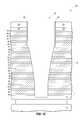
- FIG. 1shows a semiconductor construction 10 comprising a stack 16 of alternating electrically insulative levels 18 and electrically conductive levels 20 .
- the electrically conductive levels 20may comprise, for example, one or more of various metals (for example, tungsten, titanium, etc.), metal-containing compositions (for example, metal nitride, metal carbide, metal silicide, etc.), and conductively-doped semiconductor materials (for example, conductively-doped silicon, conductively-doped germanium, etc.).
- the electrically conductive levels 20may comprise n-type doped polycrystalline silicon (i.e., n-type doped polysilicon).
- the electrically insulative levels 18may, for example, comprise silicon dioxide.
- the levels 18 and 20may be of any suitable thicknesses; and may, for example, have thicknesses within a range of from about 10 nm to about 300 nm. In some applications, the levels 18 may be thinner than the levels 20 . For instance, levels 18 may be about 20 nm thick and levels 20 may be about 30 nm thick.
- the electrically conductive levels 20may be utilized to pattern control gates of flash devices.
- a vertical string of memory cellssuch as, for example, a vertical NAND string of memory cells
- the stackmay comprise any suitable number of electrically conductive levels. For instance, the stack may have 8 electrically conductive levels, 16 electrically conductive levels, 32 electrically conductive gate levels, 64 of electrically conductive levels, etc.
- the stackis over an etchstop material 14 , which is supported by a base 12 .
- a breakis provided between the etchstop material 14 and the base 12 to indicate that there may be additional materials and/or integrated circuit structures between the base and the etchstop material.
- the etchstop materialmay comprise, for example, aluminum oxide.
- the base 12may comprise semiconductor material; and may, for example, comprise, consist essentially of, or consist of monocrystalline silicon.
- the base 12may be referred to as a semiconductor substrate.
- semiconductor substratemeans any construction comprising semiconductive material, including, but not limited to, bulk semiconductive materials such as a semiconductive wafer (either alone or in assemblies comprising other materials), and semiconductive material layers (either alone or in assemblies comprising other materials).
- substraterefers to any supporting structure, including, but not limited to, the semiconductor substrates described above.
- the base 12may correspond to a semiconductor substrate containing one or more materials associated with integrated circuit fabrication. Such materials may include, for example, one or more of refractory metal materials, barrier materials, diffusion materials, insulator materials, etc.
- a hardmask material 22is over stack 16 , and a carbon-containing material 24 is over the hardmask material.
- Hardmask material 22may comprise, for example, silicon nitride.
- the carbon-containing material 24may comprise, for example, amorphous carbon.
- FIG. 2shows a patterned mask 26 provided over material 24 .
- the maskdefines an opening 28 which is patterned into materials 22 and 24 ; and such opening is then extended through stack 16 with an etch.
- the mask 26may comprise a lithographic mask (e.g., photolithographically-patterned photoresist), or a mask formed with sub-lithographic processing (e.g., pitch multiplication methodologies).
- FIGS. 1 and 2are diagrammatic cross-sectional views of a semiconductor construction at process stages of a prior method of forming integrated structures.
- FIGS. 3-10are diagrammatic cross-sectional views of a semiconductor construction at process stages of an example embodiment method of forming integrated structures.
- the processing stage of FIG. 3may follow that of FIG. 1 .
- FIGS. 11 and 12are diagrammatic cross-sectional views of a semiconductor construction at process stages of another example embodiment method of forming integrated structures.
- the processing stage of FIG. 11may follow that of FIG. 3 .
- FIGS. 13 and 14are diagrammatic cross-sectional views of a semiconductor construction at process stages of another example embodiment method of forming integrated structures.
- the processing stage of FIG. 13may follow that of FIG. 4 .
- new liner technologiesare utilized to alleviate or prevent the problems described above in the “Background” section. Example embodiments are described with reference to FIGS. 3-14 .
- the construction 10 acomprises the stack 16 of alternating electrically insulative levels 18 and electrically conductive levels 20 .
- the alternating levels 18 and 20are example alternating levels that may be utilized in some embodiments.
- the levels 18 and 20may be more generally referred to as first and second levels, respectively, to indicate that the levels may or may not be the illustrated electrically insulative levels and electrically conductive levels.
- levels 18may comprise, consist essentially of, or consist of silicon dioxide; and levels 20 may comprise, consist essentially, or consist of conductively-doped silicon (for instance, conductively-doped polycrystalline silicon).
- the stack 16is formed over etchstop material 14 , which is supported by base 12 .
- the hardmask material 22 and carbon-containing material 24are over the stack 16 .
- An opening 40is formed to extend through materials 22 and 24 , and partially through the stack 16 .
- the location of the openingmay be defined by a patterned mask (not shown) such as a mask analogous to the prior art mask 26 shown in FIG. 2 .
- the openingmay be formed with any suitable etch or combination of etches. For instance, in some embodiments a first etching composition may be utilized to extend the opening through the hardmask 22 , and then a second etching composition may be utilized to extend the opening partially through stack 16 .
- the etching composition utilized to extend the opening partially through stack 16may comprise halogen and/or carbon; and in some embodiments may comprise one or more of HBr, CH 2 F 2 , CH 4 , C 2 H 2 , H 2 , NF 3 , C 4 F 8 , C 4 F 6 , O 2 , Ar, CHF 3 , CH 3 F, BCl 3 and SF 6 .
- the opening 40has a width “W”.
- Wmay be less 100 nm, less than 80 nm, or less than 60 nm.
- such widthmay be within a range of from about 50 nm to about 80 nm.
- the opening 40may be formed to any suitable depth within stack 16 .
- the openingmay be formed to a depth which is within a range of from about one-third of the thickness of stack 16 to about two-thirds of the thickness of the stack.
- the opening 40has sidewalls 41 along stack 16 , and in the shown embodiment such sidewalls also extend along hardmask material 22 and carbon-containing material 24 .
- the openingmay be a closed shape when viewed from above (for instance, a circle, ellipse, rectangle, square, etc.) so that the illustrated sidewalls 41 are part of a continuous sidewall that extends around such closed shape.
- a liner 44 of material 42is formed within opening 40 .
- the liner material 42extends along sidewalls 41 , and also along a bottom of opening 40 .
- the liner materialmay comprise any suitable composition or combination of compositions.
- the lineris sacrificial and accordingly may comprise any of a wide variety of materials, including one or more of electrically conductive materials, semiconductor materials, and electrically insulative materials.
- the liner materialmay comprise, consist essentially of, or consist of one or more of tungsten silicide, titanium nitride, silicon nitride, carbon and polycrystalline silicon.
- the liner materialmay additionally or alternatively comprise, consist essentially of, or consist of one or more oxides having dielectric constants greater than the dielectric constant of silicon dioxide.
- oxidesmay include, for example, aluminum oxide, hafnium oxide, zirconium oxide, hafnium silicate, zirconium silicate, etc.
- the liner materialmay be of an appropriate composition to adhere to the materials 22 and 24 , as well as to the materials of stack 16 .
- the liner material 42may have any suitable thickness “T”, and in some embodiments such thickness may be within a range of from greater than 0 nanometers (nm) to about 20 nm; such as, for example, within a range of from about 4 nm to about 10 nm.
- the liner materialmay be formed with any suitable methodology, including, for example, one or more of atomic layer deposition (ALD), chemical vapor deposition (CVD) and physical vapor deposition (PVD). In some embodiments, the liner material may be formed with processing that does not exceed about 600° C. in order to avoid undesired thermal degradation of materials that may be associated with construction 10 a.
- liner material 42is removed from along the bottom of opening 40 , and the opening 40 is extended into stack 16 .
- anisotropic etching conditionsare utilized which are suitable to both remove the liner material and to penetrate through the levels 18 and 20 of stack 16 .
- the stack 16may comprise alternating levels 18 and 20 of silicon dioxide and conductively-doped silicon; the liner may comprise one or more of silicon nitride, carbon, polycrystalline silicon, titanium nitride and tungsten silicide; and the etching conditions may utilize one or more of HBr, CH 2 F 2 , CH 4 , C 2 H 2 , H 2 , NF 3 , C 4 F 8 , C 4 F 6 , O 2 , Ar, CHF 3 , CH 3 F, BCl 3 and SF 6 in an anisotropic etch.
- the etching conditionsmay be suitable for removing liner material 42 , as well as for removing materials of levels 18 and 20 .
- the anisotropic etchingwill remove liner material 42 from horizontal surfaces (specifically from over a top surface of material 24 , and from the bottom of the opening 40 in the shown embodiment) faster than from vertical surfaces (specifically, the surfaces along sidewalls 41 ).
- the etching conditionsmay include plasma.
- the anisotropic etchingremoves some of the liner material 42 from along vertical surfaces (as diagrammatically illustrated using arrows 45 ) and then redeposits such liner material along surfaces of stack 16 exposed beneath liner 44 (as diagrammatically illustrated using arrows 47 ).
- the redeposited liner materialmay be a passivation material 50 which protects sidewalls 51 of regions of opening 40 beneath liner 44 .
- the passivation material 50may comprise redeposited nitrogen.
- the regions of opening 40 beneath the linermay be referred to as a second opening, and the initial opening 40 formed at the processing stage of FIG. 3 may be referred to as a first opening.
- passivation material 50can protect materials 16 and 18 along sidewalls of opening 40 from being over-etched, which may alleviate or prevent some of the problems described above in the “Background” section; such as the divots 30 and the bowing 32 that are shown in prior art FIG. 2 .
- Another advantage of the formation of passivation material 50is that such may improve effectiveness of etching within openings 40 by limiting undesired reaction of the etchant with sidewalls of the opening. Specifically, etchant that reacts with sidewalls to form divots or bowing may be depleted in reactive material so that the etch becomes less effective for extending the opening downward.
- the passivation material 50can preclude undesired reactions with sidewalls of the opening, which may enable more effective etching from the bottom of the opening. Such can reduce the undesired narrowing of the bottom of the opening described above with reference to prior art FIG. 2 .
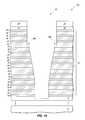
- FIG. 6shows construction 10 a at a processing stage subsequent to that of FIG. 5 and shows opening 40 deeper, while liner 44 is thinner.
- the passivation material 50lines a region of the opening beneath liner 44 , but does not line the deepest region of the opening. Accordingly, the processing stage of FIG. 6 shows three zones formed within opening 40 during the etch through stack 16 .
- an upper zone 60corresponds to a region of the opening in which sidewalls are protected by liner 44
- an intermediate zone 62corresponds to a region of the opening in which sidewalls are protected by passivation material 50 but not the liner
- a lower zone 64corresponds to a region of the opening in which sidewalls are not protected by either the liner or the passivation material. Dashed lines are provided to diagrammatically illustrate boundaries of the zones.
- a ridge 66is illustrated to occur at a region where the first zone 60 transitions into the second zone 62 ; and specifically the ridge is illustrated to be adjacent the bottom of liner 44 .
- Such ridgeis a minor perturbation on the overall shape of the opening, and is not problematic to the same extent that the defects described above with reference to FIG. 2 are problematic.
- the opening 40may have a closed shape when viewed from above (as described previously), and accordingly the ridge 66 may be a continuous ridge that extends entirely around the opening.
- construction 10 ais shown at the conclusion of an etch through stack 16 .
- the etchhas partially penetrated into etchstop material 14 .
- the etchmay stop at an upper surface of etchstop material 14 rather than penetrating into the etchstop material; and in yet other embodiments the etchstop material may be omitted or replaced with a material which is entirely penetrated by the etch.
- the liner material 42 ( FIG. 6 ) and passivation material 50 ( FIG. 6 )are entirely consumed by the time that the etch has penetrated entirely through stack 16 .
- the liner material and/or passivation materialmay be less than entirely consumed, and may be removed with a subsequent etch.
- the opening 40may have a high aspect ratio, such as an aspect ratio in excess of 30, in excess of 40, etc. (where aspect ratio refers to the depth of an etched area divided by diameter of a circular opening, or divided by the width of a non-circular opening or trench). In some embodiments, opening 40 may have a depth in excess of 3000 nm, and a width of less than 80 nm, less than 60 nm, etc.
- the opening 40 of FIG. 7has a better configuration than the prior art opening 28 of FIG. 2 . Specifically, the opening 40 of FIG. 7 lacks the divots 30 and bowing 32 of the opening 28 of FIG. 2 , and has less narrowing at the bottom than does the prior art opening of FIG. 2 .
- the opening 40 of FIG. 7retains the ridge 66 in the shown embodiment.
- the material 24( FIG. 6 ) is shown to be entirely removed at the conclusion of the etch utilized to form opening 40 . In other embodiments, some of the material 24 may remain.
- the stacked levels 18 and 20may be utilized for fabrication of integrated structures, such as, for example, memory structures, wiring, logic structures, etc. In some embodiments the stacked levels may be utilized for forming vertically-stacked memory cells, as described with reference to FIGS. 8-10 .
- cavities 68are formed to extend into the electrically conductive levels 20 .
- Such cavitiesmay be formed with an isotropic etch selective for the material of conductive levels 20 relative to the material of insulative levels 18 .
- conductive levels 20comprise conductively-doped silicon.
- liner material 42FIG. 6
- the linermay comprise material which is which is substantially entirely removed during the etch utilized to extend opening 40 through stack 16 , but which leaves some residual material within the opening. Such residual material may then be removed during the formation of cavities 68 .
- the linermay comprise polycrystalline silicon, and any residual material of the liner may be removed during the isotropic etch into the silicon of levels 20 .
- evidence of ridges 66remains along some of the levels 18 at the processing stage of FIG. 8 .
- charge blocking dielectric 70(only some of which is labeled) and charge-storage structures 72 (only some of which are labeled) are formed within cavities 68 ( FIG. 8 ).
- the charge blocking dielectricmay comprise any suitable composition or combination of compositions; and in some embodiments may comprise one or more of silicon nitride, silicon dioxide, hafnium oxide, zirconium oxide, etc.
- the charge-storage materialmay comprise any suitable composition or combination of compositions; and in some embodiments may comprise floating gate material (for instance, doped or undoped silicon) or charge-trapping material (for instance, silicon nitride, metal dots, etc.).
- charge storage structuresmay not be formed in all of the cavities. For instance, either or both of the depicted top and bottom conductive levels of the stack may be utilized as gates for drain and/or source select transistors in some embodiments.
- gate dielectric 74is formed to line opening 40 , and channel material 76 is formed within the lined opening.
- the gate dielectric materialmay comprise any suitable composition or combination of compositions; and in some embodiments may comprise one or more of silicon dioxide, hafnium oxide, zirconium oxide, aluminum oxide, etc.
- the channel materialmay comprise any suitable composition or combination of compositions; and in some embodiments may comprise appropriately-doped silicon.
- the construction of FIG. 10may comprise vertically-stacked memory cells 79 (only one of which is labeled). In some embodiments, such memory cells may be incorporated into a NAND memory array.
- a liner of the type shown in FIG. 4may be formed to comprise two or more compositions.
- FIG. 11shows a construction 10 b at a processing stage analogous to that of FIG. 4 , but utilizing a liner material 42 a comprising two discrete and different compositions 80 and 82 .
- the silicon nitridemay provide advantages for formation of passivation material (analogous to the material 50 described above with reference to FIG. 5 ), and the polycrystalline silicon may provide advantages in that any residual material can be polycrystalline which may be readily removed during formation of cavities analogous to the cavities 68 described above with reference to FIG. 8 .
- the liner material 42 amay be formed to any suitable thickness; and in some embodiments may be formed to a thickness of from greater than 0 nm to less than or equal to about 20 nm. For instance, in some embodiments both of the compositions 80 and 82 may be formed to thicknesses within a range of from greater than 0 nm to less than or equal to about 10 nm.
- construction 10 bis shown at a processing stage analogous to that described above with reference to FIG. 7 , and specifically is shown after opening 40 is extended through alternating levels 18 and 20 of stack 16 .
- the entirety of composition 82( FIG. 11 ) has been consumed during formation of the opening, but some residual of composition 80 remains. If composition 80 comprises polycrystalline silicon, such residual may be removed during anisotropic etching analogous to the etching described above with reference to FIG. 8 .
- FIG. 13shows a construction 10 c at a processing stage analogous to that of FIG. 7 , but utilizing a liner 44 b comprising a material 42 b which is not consumed during etching into stack 16 .
- the liner 44 bmay advantageously be very thin (in other words, may have a thickness of from greater than 0 nm to less than or equal to about 20 nm; and in some embodiments may have a thickness of from about 4 nm to about 10 nm); which can enable such liner to be readily removed in subsequent processing.
- the linermay comprise a high k oxide; with the term “high k” meaning a dielectric constant greater than that of silicon dioxide.
- Example high k oxidesinclude aluminum oxide, hafnium oxide, zirconium oxide, hafnium silicate, zirconium silicate, etc.
- FIG. 14shows construction 10 c at a processing stage subsequent to that of FIG. 13 , and after liner 44 b ( FIG. 13 ) has been removed.
- a ridge 66 bremains where a bottom of liner 44 b ( FIG. 13 ) rested on a level 18 .
- the ridge 66 bis analogous to the ridge 66 of FIG. 7 , but may have a more angular corner than ridge 66 in some embodiments.
- Processing described hereinmay be utilized for fabrication of high aspect ratio openings through various stacks of materials.
- the processingmay be utilized for forming high aspect openings through alternating stacks of conductively-doped silicon and silicon dioxide during fabrication of NAND.
- the openingsmay be formed through other alternating stacks.
- an alternating stack of silicon nitride and conductively-doped siliconmay be patterned (for instance, levels 18 and 20 of FIG. 7 may correspond to silicon nitride and conductively-doped silicon, respectively).
- a linermay comprise any of the materials described above as being suitable for liner 44 and/or may comprise silicon dioxide.
- Such electronic systemsmay be used in, for example, memory modules, device drivers, power modules, communication modems, processor modules, and application-specific modules, and may include multilayer, multichip modules.
- the electronic systemsmay be any of a broad range of systems, such as, for example, clocks, televisions, cell phones, personal computers, automobiles, industrial control systems, aircraft, etc.
- integrated structuremeans any structure utilized in integrated circuitry; such as structures supported by silicon chips, and including structures utilized in integrated memory, integrated logic, etc.
- dielectricand “electrically insulative” are both utilized to describe materials having insulative electrical properties. Both terms are considered synonymous in this disclosure.
- Some embodimentsinclude a method of fabricating integrated structures.
- An openingis formed to extend partially through a stack of alternating first and second levels.
- a lineris formed along sidewalls of the opening. The opening is extended into the stack utilizing etching conditions that penetrate the first and second levels and that remove substantially all of the liner.
- Some embodimentsinclude a method of fabricating integrated structures.
- An openingis formed to extend partially through a stack of alternating first and second levels.
- a lineris formed along sidewalls of the opening.
- the linerhas a thickness within a range of from greater than 0 nanometers to about 20 nanometers. While the liner is along the sidewalls, the opening is extended into the stack.
- Some embodimentsinclude a method of fabricating integrated structures.
- a first openingis formed to extend partially through a stack of alternating first and second levels.
- a lineris formed along sidewalls of the first opening.
- the linerhas a thickness within a range of from greater than 0 nanometers to about 20 nanometers.
- the openingis extended into the stack with an etch to form a second opening.
- the lineris at least partially consumed during the etch and forms passivation material which protects sidewalls of a region of the second opening beneath the liner.
- Some embodimentsinclude a method of forming vertically-stacked memory cells.
- An openingis formed to extend partially through a stack of alternating silicon dioxide levels and conductively-doped silicon levels.
- a lineris formed along sidewalls of the opening.
- the stackis etched to extend the opening.
- the lineris at least partially consumed during the etch and forms passivation material.
- Three zonesoccur during the etch, with one of the zones being an upper zone of the opening protected by the liner, another of the zones being an intermediate zone of the opening protected by passivation material but not the liner, and another of the zones being a lower zone of the opening which is not protected by either passivation material or the liner.
- Cavitiesare formed to extend into the conductively-doped silicon levels along sidewalls of the opening. Charge blocking dielectric and charge-storage structures are formed within the cavities.
Landscapes
- Engineering & Computer Science (AREA)
- Physics & Mathematics (AREA)
- Manufacturing & Machinery (AREA)
- Condensed Matter Physics & Semiconductors (AREA)
- General Physics & Mathematics (AREA)
- Computer Hardware Design (AREA)
- Microelectronics & Electronic Packaging (AREA)
- Power Engineering (AREA)
- Inorganic Chemistry (AREA)
- Chemical & Material Sciences (AREA)
- Plasma & Fusion (AREA)
- Semiconductor Memories (AREA)
- Non-Volatile Memory (AREA)
Abstract
Description
- Methods of fabricating integrated structures, and methods of forming vertically-stacked memory cells.
- Memory provides data storage for electronic systems. Flash memory is one type of memory, and has numerous uses in modern computers and devices. For instance, modern personal computers may have BIOS stored on a flash memory chip. As another example, it is becoming increasingly common for computers and other devices to utilize flash memory in solid state drives to replace conventional hard drives. As yet another example, flash memory is popular in wireless electronic devices because it enables manufacturers to support new communication protocols as they become standardized, and to provide the ability to remotely upgrade the devices for enhanced features.
- NAND may be a basic architecture of flash memory. A NAND cell unit comprises at least one selecting device coupled in series to a serial combination of memory cells (with the serial combination commonly being referred to as a NAND string). Example NAND architecture is described in U.S. Pat. No. 7,898,850. NAND architecture may be configured to comprise vertically-stacked memory cells. Fabrication of the vertically-stacked memory cells may comprise forming openings through a tall stack of alternating electrically conductive levels and electrically insulative levels, which becomes increasingly difficult with higher aspect ratio and smaller critical dimensions of the openings.
FIGS. 1 and 2 describe some of the difficulties encountered during fabrication of such openings FIG. 1 shows asemiconductor construction 10 comprising astack 16 of alternating electricallyinsulative levels 18 and electricallyconductive levels 20. The electricallyconductive levels 20 may comprise, for example, one or more of various metals (for example, tungsten, titanium, etc.), metal-containing compositions (for example, metal nitride, metal carbide, metal silicide, etc.), and conductively-doped semiconductor materials (for example, conductively-doped silicon, conductively-doped germanium, etc.). For instance, the electricallyconductive levels 20 may comprise n-type doped polycrystalline silicon (i.e., n-type doped polysilicon). The electricallyinsulative levels 18 may, for example, comprise silicon dioxide.- The
levels levels 18 may be thinner than thelevels 20. For instance,levels 18 may be about 20 nm thick andlevels 20 may be about 30 nm thick. - The electrically
conductive levels 20 may be utilized to pattern control gates of flash devices. In such applications, a vertical string of memory cells (such as, for example, a vertical NAND string of memory cells) may be fabricated, with the number of memory cells in each string being determined by the number of electricallyconductive levels 20. The stack may comprise any suitable number of electrically conductive levels. For instance, the stack may have 8 electrically conductive levels, 16 electrically conductive levels, 32 electrically conductive gate levels, 64 of electrically conductive levels, etc. - The stack is over an
etchstop material 14, which is supported by abase 12. A break is provided between theetchstop material 14 and thebase 12 to indicate that there may be additional materials and/or integrated circuit structures between the base and the etchstop material. The etchstop material may comprise, for example, aluminum oxide. - The
base 12 may comprise semiconductor material; and may, for example, comprise, consist essentially of, or consist of monocrystalline silicon. Thebase 12 may be referred to as a semiconductor substrate. The term “semiconductor substrate” means any construction comprising semiconductive material, including, but not limited to, bulk semiconductive materials such as a semiconductive wafer (either alone or in assemblies comprising other materials), and semiconductive material layers (either alone or in assemblies comprising other materials). The term “substrate” refers to any supporting structure, including, but not limited to, the semiconductor substrates described above. In some applications, thebase 12 may correspond to a semiconductor substrate containing one or more materials associated with integrated circuit fabrication. Such materials may include, for example, one or more of refractory metal materials, barrier materials, diffusion materials, insulator materials, etc. - A
hardmask material 22 is overstack 16, and a carbon-containingmaterial 24 is over the hardmask material.Hardmask material 22 may comprise, for example, silicon nitride. The carbon-containingmaterial 24 may comprise, for example, amorphous carbon. FIG. 2 shows a patternedmask 26 provided overmaterial 24. The mask defines anopening 28 which is patterned intomaterials stack 16 with an etch. Themask 26 may comprise a lithographic mask (e.g., photolithographically-patterned photoresist), or a mask formed with sub-lithographic processing (e.g., pitch multiplication methodologies).- Numerous problems are encountered in extending opening28 into the
stack 16. For instance, divots (or notches)30 form where over-etching of dielectric material oflevels 18 has occurred; bowing32 (or other anomalies in the overall shape of the opening) occur, andexcessive narrowing 34 occurs at the base of the opening. Such problems become increasing severe with increasing aspect ratios associated with higher levels of integration. It would be desired to develop methods which alleviate or prevent some or all of the problems described with reference toFIG. 2 . FIGS. 1 and 2 are diagrammatic cross-sectional views of a semiconductor construction at process stages of a prior method of forming integrated structures.FIGS. 3-10 are diagrammatic cross-sectional views of a semiconductor construction at process stages of an example embodiment method of forming integrated structures. The processing stage ofFIG. 3 may follow that ofFIG. 1 .FIGS. 11 and 12 are diagrammatic cross-sectional views of a semiconductor construction at process stages of another example embodiment method of forming integrated structures. The processing stage ofFIG. 11 may follow that ofFIG. 3 .FIGS. 13 and 14 are diagrammatic cross-sectional views of a semiconductor construction at process stages of another example embodiment method of forming integrated structures. The processing stage ofFIG. 13 may follow that ofFIG. 4 .- In some embodiments, new liner technologies are utilized to alleviate or prevent the problems described above in the “Background” section. Example embodiments are described with reference to
FIGS. 3-14 . - Referring to
FIG. 3 , asemiconductor construction 10ais shown at a processing stage which may follow the prior art processing stage described above with reference toFIG. 1 . Theconstruction 10acomprises thestack 16 of alternating electricallyinsulative levels 18 and electricallyconductive levels 20. Thealternating levels levels levels 18 may comprise, consist essentially of, or consist of silicon dioxide; andlevels 20 may comprise, consist essentially, or consist of conductively-doped silicon (for instance, conductively-doped polycrystalline silicon). - The
stack 16 is formed overetchstop material 14, which is supported bybase 12. - The
hardmask material 22 and carbon-containingmaterial 24 are over thestack 16. - An
opening 40 is formed to extend throughmaterials stack 16. The location of the opening may be defined by a patterned mask (not shown) such as a mask analogous to theprior art mask 26 shown inFIG. 2 . The opening may be formed with any suitable etch or combination of etches. For instance, in some embodiments a first etching composition may be utilized to extend the opening through thehardmask 22, and then a second etching composition may be utilized to extend the opening partially throughstack 16. The etching composition utilized to extend the opening partially throughstack 16 may comprise halogen and/or carbon; and in some embodiments may comprise one or more of HBr, CH2F2, CH4, C2H2, H2, NF3, C4F8, C4F6, O2, Ar, CHF3, CH3F, BCl3and SF6. - The
opening 40 has a width “W”. In some embodiments, such width may be less 100 nm, less than 80 nm, or less than 60 nm. For instance, in some embodiments such width may be within a range of from about 50 nm to about 80 nm. - The
opening 40 may be formed to any suitable depth withinstack 16. For instance, in some embodiments the opening may be formed to a depth which is within a range of from about one-third of the thickness ofstack 16 to about two-thirds of the thickness of the stack. - The
opening 40 has sidewalls41 alongstack 16, and in the shown embodiment such sidewalls also extend alonghardmask material 22 and carbon-containingmaterial 24. The opening may be a closed shape when viewed from above (for instance, a circle, ellipse, rectangle, square, etc.) so that the illustratedsidewalls 41 are part of a continuous sidewall that extends around such closed shape. - Referring to
FIG. 4 , aliner 44 ofmaterial 42 is formed withinopening 40. Theliner material 42 extends alongsidewalls 41, and also along a bottom ofopening 40. The liner material may comprise any suitable composition or combination of compositions. In some embodiments, the liner is sacrificial and accordingly may comprise any of a wide variety of materials, including one or more of electrically conductive materials, semiconductor materials, and electrically insulative materials. In some embodiments, the liner material may comprise, consist essentially of, or consist of one or more of tungsten silicide, titanium nitride, silicon nitride, carbon and polycrystalline silicon. In some embodiments, the liner material may additionally or alternatively comprise, consist essentially of, or consist of one or more oxides having dielectric constants greater than the dielectric constant of silicon dioxide. Such oxides may include, for example, aluminum oxide, hafnium oxide, zirconium oxide, hafnium silicate, zirconium silicate, etc. The liner material may be of an appropriate composition to adhere to thematerials stack 16. - The
liner material 42 may have any suitable thickness “T”, and in some embodiments such thickness may be within a range of from greater than 0 nanometers (nm) to about 20 nm; such as, for example, within a range of from about 4 nm to about 10 nm. The liner material may be formed with any suitable methodology, including, for example, one or more of atomic layer deposition (ALD), chemical vapor deposition (CVD) and physical vapor deposition (PVD). In some embodiments, the liner material may be formed with processing that does not exceed about 600° C. in order to avoid undesired thermal degradation of materials that may be associated withconstruction 10a. - Referring to
FIG. 5 ,liner material 42 is removed from along the bottom of opening40, and theopening 40 is extended intostack 16. In some embodiments, anisotropic etching conditions are utilized which are suitable to both remove the liner material and to penetrate through thelevels stack 16. - In some embodiments, the
stack 16 may comprise alternatinglevels liner material 42, as well as for removing materials oflevels liner material 42 from horizontal surfaces (specifically from over a top surface ofmaterial 24, and from the bottom of theopening 40 in the shown embodiment) faster than from vertical surfaces (specifically, the surfaces along sidewalls41). In some embodiments, the etching conditions may include plasma. - In some embodiments, the anisotropic etching removes some of the
liner material 42 from along vertical surfaces (as diagrammatically illustrated using arrows45) and then redeposits such liner material along surfaces ofstack 16 exposed beneath liner44 (as diagrammatically illustrated using arrows47). The redeposited liner material may be apassivation material 50 which protects sidewalls51 of regions of opening40 beneathliner 44. For instance, if theliner 44 comprises silicon nitride, thepassivation material 50 may comprise redeposited nitrogen. In some embodiments, the regions of opening40 beneath the liner may be referred to as a second opening, and theinitial opening 40 formed at the processing stage ofFIG. 3 may be referred to as a first opening. - An advantage of the formation of
passivation material 50 is that such can protectmaterials divots 30 and the bowing32 that are shown in prior artFIG. 2 . Another advantage of the formation ofpassivation material 50 is that such may improve effectiveness of etching withinopenings 40 by limiting undesired reaction of the etchant with sidewalls of the opening. Specifically, etchant that reacts with sidewalls to form divots or bowing may be depleted in reactive material so that the etch becomes less effective for extending the opening downward. Thepassivation material 50 can preclude undesired reactions with sidewalls of the opening, which may enable more effective etching from the bottom of the opening. Such can reduce the undesired narrowing of the bottom of the opening described above with reference to prior artFIG. 2 . - The
liner 44 is consumed as opening40 is extended deeper intostack 16.FIG. 6 showsconstruction 10aat a processing stage subsequent to that ofFIG. 5 and showsopening 40 deeper, whileliner 44 is thinner. Thepassivation material 50 lines a region of the opening beneathliner 44, but does not line the deepest region of the opening. Accordingly, the processing stage ofFIG. 6 shows three zones formed within opening40 during the etch throughstack 16. Specifically, anupper zone 60 corresponds to a region of the opening in which sidewalls are protected byliner 44, anintermediate zone 62 corresponds to a region of the opening in which sidewalls are protected bypassivation material 50 but not the liner, and alower zone 64 corresponds to a region of the opening in which sidewalls are not protected by either the liner or the passivation material. Dashed lines are provided to diagrammatically illustrate boundaries of the zones. - A
ridge 66 is illustrated to occur at a region where thefirst zone 60 transitions into thesecond zone 62; and specifically the ridge is illustrated to be adjacent the bottom ofliner 44. Such ridge is a minor perturbation on the overall shape of the opening, and is not problematic to the same extent that the defects described above with reference toFIG. 2 are problematic. Although there appear to be two ridges in the cross-section ofFIG. 6 , theopening 40 may have a closed shape when viewed from above (as described previously), and accordingly theridge 66 may be a continuous ridge that extends entirely around the opening. - Referring to
FIG. 7 ,construction 10ais shown at the conclusion of an etch throughstack 16. The etch has partially penetrated intoetchstop material 14. In other embodiments, the etch may stop at an upper surface ofetchstop material 14 rather than penetrating into the etchstop material; and in yet other embodiments the etchstop material may be omitted or replaced with a material which is entirely penetrated by the etch. - In the illustrated embodiment, the liner material42 (
FIG. 6 ) and passivation material50 (FIG. 6 ) are entirely consumed by the time that the etch has penetrated entirely throughstack 16. In other embodiments, the liner material and/or passivation material may be less than entirely consumed, and may be removed with a subsequent etch. - The
opening 40 may have a high aspect ratio, such as an aspect ratio in excess of 30, in excess of 40, etc. (where aspect ratio refers to the depth of an etched area divided by diameter of a circular opening, or divided by the width of a non-circular opening or trench). In some embodiments, opening40 may have a depth in excess of 3000 nm, and a width of less than 80 nm, less than 60 nm, etc. Theopening 40 ofFIG. 7 has a better configuration than theprior art opening 28 ofFIG. 2 . Specifically, theopening 40 ofFIG. 7 lacks thedivots 30 and bowing32 of theopening 28 ofFIG. 2 , and has less narrowing at the bottom than does the prior art opening ofFIG. 2 . - The
opening 40 ofFIG. 7 retains theridge 66 in the shown embodiment. In some embodiments, it may be advantageous to utilize the processing ofFIGS. 3-7 to penetrate partially through a stack, and to then repeat such processing at least one additional time to penetrate the remainder of the way to the stack. Each time that the processing is repeated, there may be a ridge analogous to theridge 66 formed at a location where there had been the bottom of a liner (analogous to theliner 44 ofFIG. 6 ). - The material24 (
FIG. 6 ) is shown to be entirely removed at the conclusion of the etch utilized to formopening 40. In other embodiments, some of the material24 may remain. - The stacked
levels FIGS. 8-10 . - Referring to
FIG. 8 , cavities68 (only some of which are labeled) are formed to extend into the electricallyconductive levels 20. Such cavities may be formed with an isotropic etch selective for the material ofconductive levels 20 relative to the material ofinsulative levels 18. In some embodiments,conductive levels 20 comprise conductively-doped silicon. In such embodiments, liner material42 (FIG. 6 ) may comprise material which is which is substantially entirely removed during the etch utilized to extendopening 40 throughstack 16, but which leaves some residual material within the opening. Such residual material may then be removed during the formation ofcavities 68. For instance, the liner may comprise polycrystalline silicon, and any residual material of the liner may be removed during the isotropic etch into the silicon oflevels 20. - In the shown embodiment, evidence of
ridges 66 remains along some of thelevels 18 at the processing stage ofFIG. 8 . - Referring to
FIG. 9 charge blocking dielectric70 (only some of which is labeled) and charge-storage structures72 (only some of which are labeled) are formed within cavities68 (FIG. 8 ). The charge blocking dielectric may comprise any suitable composition or combination of compositions; and in some embodiments may comprise one or more of silicon nitride, silicon dioxide, hafnium oxide, zirconium oxide, etc. The charge-storage material may comprise any suitable composition or combination of compositions; and in some embodiments may comprise floating gate material (for instance, doped or undoped silicon) or charge-trapping material (for instance, silicon nitride, metal dots, etc.). In some embodiments, charge storage structures may not be formed in all of the cavities. For instance, either or both of the depicted top and bottom conductive levels of the stack may be utilized as gates for drain and/or source select transistors in some embodiments. - Referring to
FIG. 10 ,gate dielectric 74 is formed toline opening 40, andchannel material 76 is formed within the lined opening. The gate dielectric material may comprise any suitable composition or combination of compositions; and in some embodiments may comprise one or more of silicon dioxide, hafnium oxide, zirconium oxide, aluminum oxide, etc. The channel material may comprise any suitable composition or combination of compositions; and in some embodiments may comprise appropriately-doped silicon. The construction ofFIG. 10 may comprise vertically-stacked memory cells79 (only one of which is labeled). In some embodiments, such memory cells may be incorporated into a NAND memory array. - In some embodiments, a liner of the type shown in
FIG. 4 may be formed to comprise two or more compositions. For instance,FIG. 11 shows aconstruction 10bat a processing stage analogous to that ofFIG. 4 , but utilizing aliner material 42acomprising two discrete anddifferent compositions liner 42ato comprise afirst composition 80 of polycrystalline silicon, and asecond composition 82 of silicon nitride. The silicon nitride may provide advantages for formation of passivation material (analogous to the material50 described above with reference toFIG. 5 ), and the polycrystalline silicon may provide advantages in that any residual material can be polycrystalline which may be readily removed during formation of cavities analogous to thecavities 68 described above with reference toFIG. 8 . Theliner material 42amay be formed to any suitable thickness; and in some embodiments may be formed to a thickness of from greater than 0 nm to less than or equal to about 20 nm. For instance, in some embodiments both of thecompositions - Referring to
FIG. 12 ,construction 10bis shown at a processing stage analogous to that described above with reference toFIG. 7 , and specifically is shown after opening40 is extended through alternatinglevels stack 16. The entirety of composition82 (FIG. 11 ) has been consumed during formation of the opening, but some residual ofcomposition 80 remains. Ifcomposition 80 comprises polycrystalline silicon, such residual may be removed during anisotropic etching analogous to the etching described above with reference toFIG. 8 . - The embodiments described above utilize liner material which is at least partially consumed as an opening is extended into a stack of alternating levels. In other embodiments, analogous liners may be constructed of materials which are substantially not consumed. For instance,
FIG. 13 shows aconstruction 10cat a processing stage analogous to that ofFIG. 7 , but utilizing aliner 44bcomprising a material42bwhich is not consumed during etching intostack 16. Theliner 44bmay advantageously be very thin (in other words, may have a thickness of from greater than 0 nm to less than or equal to about 20 nm; and in some embodiments may have a thickness of from about 4 nm to about 10 nm); which can enable such liner to be readily removed in subsequent processing. In some embodiments, the liner may comprise a high k oxide; with the term “high k” meaning a dielectric constant greater than that of silicon dioxide. Example high k oxides include aluminum oxide, hafnium oxide, zirconium oxide, hafnium silicate, zirconium silicate, etc. FIG. 14 showsconstruction 10cat a processing stage subsequent to that ofFIG. 13 , and afterliner 44b(FIG. 13 ) has been removed. Aridge 66bremains where a bottom ofliner 44b(FIG. 13 ) rested on alevel 18. Theridge 66bis analogous to theridge 66 ofFIG. 7 , but may have a more angular corner thanridge 66 in some embodiments.- Processing described herein may be utilized for fabrication of high aspect ratio openings through various stacks of materials. In some embodiments, the processing may be utilized for forming high aspect openings through alternating stacks of conductively-doped silicon and silicon dioxide during fabrication of NAND. In other embodiments, the openings may be formed through other alternating stacks. For instance, in some embodiments an alternating stack of silicon nitride and conductively-doped silicon may be patterned (for instance,
levels FIG. 7 may correspond to silicon nitride and conductively-doped silicon, respectively). In such embodiments, a liner may comprise any of the materials described above as being suitable forliner 44 and/or may comprise silicon dioxide. - The constructions discussed above may be utilized for fabrication of integrated structures which are incorporated into electronic systems. Such electronic systems may be used in, for example, memory modules, device drivers, power modules, communication modems, processor modules, and application-specific modules, and may include multilayer, multichip modules. The electronic systems may be any of a broad range of systems, such as, for example, clocks, televisions, cell phones, personal computers, automobiles, industrial control systems, aircraft, etc.
- The term “integrated structure” means any structure utilized in integrated circuitry; such as structures supported by silicon chips, and including structures utilized in integrated memory, integrated logic, etc.
- The terms “dielectric” and “electrically insulative” are both utilized to describe materials having insulative electrical properties. Both terms are considered synonymous in this disclosure. The utilization of the term “dielectric” in some instances, and the term “electrically insulative” in other instances, is to provide language variation within this disclosure to simplify antecedent basis within the claims that follow, and is not utilized to indicate any significant chemical or electrical differences.
- The particular orientation of the various embodiments in the drawings is for illustrative purposes only, and the embodiments may be rotated relative to the shown orientations in some applications. The description provided herein, and the claims that follow, pertain to any structures that have the described relationships between various features, regardless of whether the structures are in the particular orientation of the drawings, or are rotated relative to such orientation.
- The cross-sectional views of the accompanying illustrations only show features within the planes of the cross-sections, and do not show materials behind the planes of the cross-sections in order to simplify the drawings.
- When a structure is referred to above as being “on” or “against” another structure, it can be directly on the other structure or intervening structures may also be present. In contrast, when a structure is referred to as being “directly on” or “directly against” another structure, there are no intervening structures present. When a structure is referred to as being “connected” or “coupled” to another structure, it can be directly connected or coupled to the other structure, or intervening structures may be present. In contrast, when a structure is referred to as being “directly connected” or “directly coupled” to another structure, there are no intervening structures present.
- Some embodiments include a method of fabricating integrated structures. An opening is formed to extend partially through a stack of alternating first and second levels. A liner is formed along sidewalls of the opening. The opening is extended into the stack utilizing etching conditions that penetrate the first and second levels and that remove substantially all of the liner.
- Some embodiments include a method of fabricating integrated structures. An opening is formed to extend partially through a stack of alternating first and second levels. A liner is formed along sidewalls of the opening. The liner has a thickness within a range of from greater than 0 nanometers to about 20 nanometers. While the liner is along the sidewalls, the opening is extended into the stack.
- Some embodiments include a method of fabricating integrated structures. A first opening is formed to extend partially through a stack of alternating first and second levels. A liner is formed along sidewalls of the first opening. The liner has a thickness within a range of from greater than 0 nanometers to about 20 nanometers. The opening is extended into the stack with an etch to form a second opening. The liner is at least partially consumed during the etch and forms passivation material which protects sidewalls of a region of the second opening beneath the liner.
- Some embodiments include a method of forming vertically-stacked memory cells. An opening is formed to extend partially through a stack of alternating silicon dioxide levels and conductively-doped silicon levels. A liner is formed along sidewalls of the opening. The stack is etched to extend the opening. The liner is at least partially consumed during the etch and forms passivation material. Three zones occur during the etch, with one of the zones being an upper zone of the opening protected by the liner, another of the zones being an intermediate zone of the opening protected by passivation material but not the liner, and another of the zones being a lower zone of the opening which is not protected by either passivation material or the liner. Cavities are formed to extend into the conductively-doped silicon levels along sidewalls of the opening. Charge blocking dielectric and charge-storage structures are formed within the cavities.
- In compliance with the statute, the subject matter disclosed herein has been described in language more or less specific as to structural and methodical features. It is to be understood, however, that the claims are not limited to the specific features shown and described, since the means herein disclosed comprise example embodiments. The claims are thus to be afforded full scope as literally worded, and to be appropriately interpreted in accordance with the doctrine of equivalents.
Claims (35)
Priority Applications (5)
| Application Number | Priority Date | Filing Date | Title |
|---|---|---|---|
| US13/835,551US8946076B2 (en) | 2013-03-15 | 2013-03-15 | Methods of fabricating integrated structures, and methods of forming vertically-stacked memory cells |
| PCT/US2013/075825WO2014143277A1 (en) | 2013-03-15 | 2013-12-17 | Methods of fabricating integrated structures, and methods of forming vertically-stacked memory cells |
| KR1020157029224AKR101716608B1 (en) | 2013-03-15 | 2013-12-17 | Methods of fabricating integrated structures, and methods of forming vertically-stacked memory cells |
| CN201380075919.0ACN105144382B (en) | 2013-03-15 | 2013-12-17 | The method for manufacturing the method for integrated morphology and forming vertical stacking memory cell |
| TW102149120ATWI549180B (en) | 2013-03-15 | 2013-12-30 | Method of manufacturing integrated structure and method of forming vertically stacked memory unit |
Applications Claiming Priority (1)
| Application Number | Priority Date | Filing Date | Title |
|---|---|---|---|
| US13/835,551US8946076B2 (en) | 2013-03-15 | 2013-03-15 | Methods of fabricating integrated structures, and methods of forming vertically-stacked memory cells |
Publications (2)
| Publication Number | Publication Date |
|---|---|
| US20140273462A1true US20140273462A1 (en) | 2014-09-18 |
| US8946076B2 US8946076B2 (en) | 2015-02-03 |
Family
ID=51528977
Family Applications (1)
| Application Number | Title | Priority Date | Filing Date |
|---|---|---|---|
| US13/835,551Active2033-03-21US8946076B2 (en) | 2013-03-15 | 2013-03-15 | Methods of fabricating integrated structures, and methods of forming vertically-stacked memory cells |
Country Status (5)
| Country | Link |
|---|---|
| US (1) | US8946076B2 (en) |
| KR (1) | KR101716608B1 (en) |
| CN (1) | CN105144382B (en) |
| TW (1) | TWI549180B (en) |
| WO (1) | WO2014143277A1 (en) |
Cited By (152)
| Publication number | Priority date | Publication date | Assignee | Title |
|---|---|---|---|---|
| US20150008503A1 (en)* | 2013-07-02 | 2015-01-08 | SanDisk Technologies, Inc. | Method Of Making A Three-Dimensional Memory Array With Etch Stop |
| US9165786B1 (en)* | 2014-08-05 | 2015-10-20 | Applied Materials, Inc. | Integrated oxide and nitride recess for better channel contact in 3D architectures |
| US20150332932A1 (en)* | 2014-05-14 | 2015-11-19 | Tokyo Electron Limited | Method for etching etching target layer |
| US9269590B2 (en) | 2014-04-07 | 2016-02-23 | Applied Materials, Inc. | Spacer formation |
| US9287095B2 (en) | 2013-12-17 | 2016-03-15 | Applied Materials, Inc. | Semiconductor system assemblies and methods of operation |
| US9287134B2 (en) | 2014-01-17 | 2016-03-15 | Applied Materials, Inc. | Titanium oxide etch |
| US9293568B2 (en) | 2014-01-27 | 2016-03-22 | Applied Materials, Inc. | Method of fin patterning |
| US9299537B2 (en) | 2014-03-20 | 2016-03-29 | Applied Materials, Inc. | Radial waveguide systems and methods for post-match control of microwaves |
| US9299575B2 (en) | 2014-03-17 | 2016-03-29 | Applied Materials, Inc. | Gas-phase tungsten etch |
| US9299583B1 (en) | 2014-12-05 | 2016-03-29 | Applied Materials, Inc. | Aluminum oxide selective etch |
| US9299538B2 (en) | 2014-03-20 | 2016-03-29 | Applied Materials, Inc. | Radial waveguide systems and methods for post-match control of microwaves |
| US9309598B2 (en) | 2014-05-28 | 2016-04-12 | Applied Materials, Inc. | Oxide and metal removal |
| US9324576B2 (en) | 2010-05-27 | 2016-04-26 | Applied Materials, Inc. | Selective etch for silicon films |
| US9343272B1 (en) | 2015-01-08 | 2016-05-17 | Applied Materials, Inc. | Self-aligned process |
| US9349605B1 (en) | 2015-08-07 | 2016-05-24 | Applied Materials, Inc. | Oxide etch selectivity systems and methods |
| US9355856B2 (en) | 2014-09-12 | 2016-05-31 | Applied Materials, Inc. | V trench dry etch |
| US9355863B2 (en) | 2012-12-18 | 2016-05-31 | Applied Materials, Inc. | Non-local plasma oxide etch |
| US9355862B2 (en) | 2014-09-24 | 2016-05-31 | Applied Materials, Inc. | Fluorine-based hardmask removal |
| US9362130B2 (en) | 2013-03-01 | 2016-06-07 | Applied Materials, Inc. | Enhanced etching processes using remote plasma sources |
| US9368364B2 (en) | 2014-09-24 | 2016-06-14 | Applied Materials, Inc. | Silicon etch process with tunable selectivity to SiO2 and other materials |
| KR20160068002A (en)* | 2014-12-04 | 2016-06-14 | 램 리써치 코포레이션 | Technique to deposit metal-containing sidewall passivation for high aspect ratio cylinder etch |
| US9373522B1 (en) | 2015-01-22 | 2016-06-21 | Applied Mateials, Inc. | Titanium nitride removal |
| US9373517B2 (en) | 2012-08-02 | 2016-06-21 | Applied Materials, Inc. | Semiconductor processing with DC assisted RF power for improved control |
| US9378978B2 (en) | 2014-07-31 | 2016-06-28 | Applied Materials, Inc. | Integrated oxide recess and floating gate fin trimming |
| US9378969B2 (en) | 2014-06-19 | 2016-06-28 | Applied Materials, Inc. | Low temperature gas-phase carbon removal |
| US9384997B2 (en) | 2012-11-20 | 2016-07-05 | Applied Materials, Inc. | Dry-etch selectivity |
| US9385028B2 (en) | 2014-02-03 | 2016-07-05 | Applied Materials, Inc. | Air gap process |
| US9390937B2 (en) | 2012-09-20 | 2016-07-12 | Applied Materials, Inc. | Silicon-carbon-nitride selective etch |
| US9396989B2 (en) | 2014-01-27 | 2016-07-19 | Applied Materials, Inc. | Air gaps between copper lines |
| US9406523B2 (en) | 2014-06-19 | 2016-08-02 | Applied Materials, Inc. | Highly selective doped oxide removal method |
| US9412608B2 (en) | 2012-11-30 | 2016-08-09 | Applied Materials, Inc. | Dry-etch for selective tungsten removal |
| US9418858B2 (en) | 2011-10-07 | 2016-08-16 | Applied Materials, Inc. | Selective etch of silicon by way of metastable hydrogen termination |
| US9425058B2 (en) | 2014-07-24 | 2016-08-23 | Applied Materials, Inc. | Simplified litho-etch-litho-etch process |
| US9437451B2 (en) | 2012-09-18 | 2016-09-06 | Applied Materials, Inc. | Radical-component oxide etch |
| US9449845B2 (en) | 2012-12-21 | 2016-09-20 | Applied Materials, Inc. | Selective titanium nitride etching |
| US9449850B2 (en) | 2013-03-15 | 2016-09-20 | Applied Materials, Inc. | Processing systems and methods for halide scavenging |
| US9449846B2 (en) | 2015-01-28 | 2016-09-20 | Applied Materials, Inc. | Vertical gate separation |
| US20160284719A1 (en)* | 2015-03-23 | 2016-09-29 | Micron Technology, Inc. | Integrated Structures and Methods of Forming Vertically-Stacked Memory Cells |
| US9472412B2 (en) | 2013-12-02 | 2016-10-18 | Applied Materials, Inc. | Procedure for etch rate consistency |
| US9472417B2 (en) | 2013-11-12 | 2016-10-18 | Applied Materials, Inc. | Plasma-free metal etch |
| US9478432B2 (en) | 2014-09-25 | 2016-10-25 | Applied Materials, Inc. | Silicon oxide selective removal |
| US9493879B2 (en) | 2013-07-12 | 2016-11-15 | Applied Materials, Inc. | Selective sputtering for pattern transfer |
| US9496167B2 (en) | 2014-07-31 | 2016-11-15 | Applied Materials, Inc. | Integrated bit-line airgap formation and gate stack post clean |
| US9502429B2 (en)* | 2014-11-26 | 2016-11-22 | Sandisk Technologies Llc | Set of stepped surfaces formation for a multilevel interconnect structure |
| US9502258B2 (en) | 2014-12-23 | 2016-11-22 | Applied Materials, Inc. | Anisotropic gap etch |
| US9499898B2 (en) | 2014-03-03 | 2016-11-22 | Applied Materials, Inc. | Layered thin film heater and method of fabrication |
| US9553102B2 (en) | 2014-08-19 | 2017-01-24 | Applied Materials, Inc. | Tungsten separation |
| US9576809B2 (en) | 2013-11-04 | 2017-02-21 | Applied Materials, Inc. | Etch suppression with germanium |
| US9607856B2 (en) | 2013-03-05 | 2017-03-28 | Applied Materials, Inc. | Selective titanium nitride removal |
| US9659753B2 (en) | 2014-08-07 | 2017-05-23 | Applied Materials, Inc. | Grooved insulator to reduce leakage current |
| US9691645B2 (en) | 2015-08-06 | 2017-06-27 | Applied Materials, Inc. | Bolted wafer chuck thermal management systems and methods for wafer processing systems |
| US9721789B1 (en) | 2016-10-04 | 2017-08-01 | Applied Materials, Inc. | Saving ion-damaged spacers |
| US9728499B2 (en) | 2014-11-26 | 2017-08-08 | Sandisk Technologies Llc | Set of stepped surfaces formation for a multilevel interconnect structure |
| US9728437B2 (en) | 2015-02-03 | 2017-08-08 | Applied Materials, Inc. | High temperature chuck for plasma processing systems |
| US9741593B2 (en) | 2015-08-06 | 2017-08-22 | Applied Materials, Inc. | Thermal management systems and methods for wafer processing systems |
| US9768034B1 (en) | 2016-11-11 | 2017-09-19 | Applied Materials, Inc. | Removal methods for high aspect ratio structures |
| US9773648B2 (en) | 2013-08-30 | 2017-09-26 | Applied Materials, Inc. | Dual discharge modes operation for remote plasma |
| US9793291B2 (en) | 2015-05-21 | 2017-10-17 | Samsung Electronics Co., Ltd. | Method of manufacturing a semiconductor device |
| US9842744B2 (en) | 2011-03-14 | 2017-12-12 | Applied Materials, Inc. | Methods for etch of SiN films |
| US9865484B1 (en) | 2016-06-29 | 2018-01-09 | Applied Materials, Inc. | Selective etch using material modification and RF pulsing |
| US9881805B2 (en) | 2015-03-02 | 2018-01-30 | Applied Materials, Inc. | Silicon selective removal |
| US9887096B2 (en) | 2012-09-17 | 2018-02-06 | Applied Materials, Inc. | Differential silicon oxide etch |
| US9885117B2 (en) | 2014-03-31 | 2018-02-06 | Applied Materials, Inc. | Conditioned semiconductor system parts |
| US9934942B1 (en) | 2016-10-04 | 2018-04-03 | Applied Materials, Inc. | Chamber with flow-through source |
| US9947549B1 (en) | 2016-10-10 | 2018-04-17 | Applied Materials, Inc. | Cobalt-containing material removal |
| US9978564B2 (en) | 2012-09-21 | 2018-05-22 | Applied Materials, Inc. | Chemical control features in wafer process equipment |
| US9991118B2 (en)* | 2016-01-20 | 2018-06-05 | Applied Materials, Inc. | Hybrid carbon hardmask for lateral hardmask recess reduction |
| US20180190540A1 (en)* | 2016-12-31 | 2018-07-05 | Intel Corporation | A Solid State Memory Device, and Manufacturing Method Thereof |
| US10026621B2 (en) | 2016-11-14 | 2018-07-17 | Applied Materials, Inc. | SiN spacer profile patterning |
| US10043684B1 (en) | 2017-02-06 | 2018-08-07 | Applied Materials, Inc. | Self-limiting atomic thermal etching systems and methods |
| US10043674B1 (en) | 2017-08-04 | 2018-08-07 | Applied Materials, Inc. | Germanium etching systems and methods |
| US10049891B1 (en) | 2017-05-31 | 2018-08-14 | Applied Materials, Inc. | Selective in situ cobalt residue removal |
| US10062585B2 (en) | 2016-10-04 | 2018-08-28 | Applied Materials, Inc. | Oxygen compatible plasma source |
| US10062587B2 (en) | 2012-07-18 | 2018-08-28 | Applied Materials, Inc. | Pedestal with multi-zone temperature control and multiple purge capabilities |
| US10062579B2 (en) | 2016-10-07 | 2018-08-28 | Applied Materials, Inc. | Selective SiN lateral recess |
| US10062575B2 (en) | 2016-09-09 | 2018-08-28 | Applied Materials, Inc. | Poly directional etch by oxidation |
| US10062578B2 (en) | 2011-03-14 | 2018-08-28 | Applied Materials, Inc. | Methods for etch of metal and metal-oxide films |
| US10128086B1 (en) | 2017-10-24 | 2018-11-13 | Applied Materials, Inc. | Silicon pretreatment for nitride removal |
| US10147638B1 (en)* | 2017-12-29 | 2018-12-04 | Micron Technology, Inc. | Methods of forming staircase structures |
| CN109075166A (en)* | 2016-04-19 | 2018-12-21 | 美光科技公司 | Integrated morphology comprising the material containing at least one of silicon, nitrogen and carbon, oxygen, boron and phosphorus |
| US10163696B2 (en) | 2016-11-11 | 2018-12-25 | Applied Materials, Inc. | Selective cobalt removal for bottom up gapfill |
| US10170336B1 (en) | 2017-08-04 | 2019-01-01 | Applied Materials, Inc. | Methods for anisotropic control of selective silicon removal |
| US10224210B2 (en) | 2014-12-09 | 2019-03-05 | Applied Materials, Inc. | Plasma processing system with direct outlet toroidal plasma source |
| US10242908B2 (en) | 2016-11-14 | 2019-03-26 | Applied Materials, Inc. | Airgap formation with damage-free copper |
| US10256079B2 (en) | 2013-02-08 | 2019-04-09 | Applied Materials, Inc. | Semiconductor processing systems having multiple plasma configurations |
| US10256112B1 (en) | 2017-12-08 | 2019-04-09 | Applied Materials, Inc. | Selective tungsten removal |
| US10283321B2 (en) | 2011-01-18 | 2019-05-07 | Applied Materials, Inc. | Semiconductor processing system and methods using capacitively coupled plasma |
| US10283324B1 (en) | 2017-10-24 | 2019-05-07 | Applied Materials, Inc. | Oxygen treatment for nitride etching |
| US20190148402A1 (en)* | 2017-09-07 | 2019-05-16 | Toshiba Memory Corporation | Semiconductor device and method of fabricating the same |
| US10297458B2 (en) | 2017-08-07 | 2019-05-21 | Applied Materials, Inc. | Process window widening using coated parts in plasma etch processes |
| US10319649B2 (en) | 2017-04-11 | 2019-06-11 | Applied Materials, Inc. | Optical emission spectroscopy (OES) for remote plasma monitoring |
| US10319600B1 (en) | 2018-03-12 | 2019-06-11 | Applied Materials, Inc. | Thermal silicon etch |
| US10319739B2 (en) | 2017-02-08 | 2019-06-11 | Applied Materials, Inc. | Accommodating imperfectly aligned memory holes |
| US10354889B2 (en) | 2017-07-17 | 2019-07-16 | Applied Materials, Inc. | Non-halogen etching of silicon-containing materials |
| US10403507B2 (en) | 2017-02-03 | 2019-09-03 | Applied Materials, Inc. | Shaped etch profile with oxidation |
| US10431429B2 (en) | 2017-02-03 | 2019-10-01 | Applied Materials, Inc. | Systems and methods for radial and azimuthal control of plasma uniformity |
| US10468267B2 (en) | 2017-05-31 | 2019-11-05 | Applied Materials, Inc. | Water-free etching methods |
| US10490406B2 (en) | 2018-04-10 | 2019-11-26 | Appled Materials, Inc. | Systems and methods for material breakthrough |
| US10490418B2 (en) | 2014-10-14 | 2019-11-26 | Applied Materials, Inc. | Systems and methods for internal surface conditioning assessment in plasma processing equipment |
| US10497573B2 (en) | 2018-03-13 | 2019-12-03 | Applied Materials, Inc. | Selective atomic layer etching of semiconductor materials |
| US10504700B2 (en) | 2015-08-27 | 2019-12-10 | Applied Materials, Inc. | Plasma etching systems and methods with secondary plasma injection |
| US10504754B2 (en) | 2016-05-19 | 2019-12-10 | Applied Materials, Inc. | Systems and methods for improved semiconductor etching and component protection |
| US10522371B2 (en) | 2016-05-19 | 2019-12-31 | Applied Materials, Inc. | Systems and methods for improved semiconductor etching and component protection |
| US10541184B2 (en) | 2017-07-11 | 2020-01-21 | Applied Materials, Inc. | Optical emission spectroscopic techniques for monitoring etching |
| US10541246B2 (en) | 2017-06-26 | 2020-01-21 | Applied Materials, Inc. | 3D flash memory cells which discourage cross-cell electrical tunneling |
| US10546729B2 (en) | 2016-10-04 | 2020-01-28 | Applied Materials, Inc. | Dual-channel showerhead with improved profile |
| US20200035505A1 (en)* | 2018-07-27 | 2020-01-30 | Applied Materials, Inc. | 3D NAND Etch |
| US10566206B2 (en) | 2016-12-27 | 2020-02-18 | Applied Materials, Inc. | Systems and methods for anisotropic material breakthrough |
| US10573496B2 (en) | 2014-12-09 | 2020-02-25 | Applied Materials, Inc. | Direct outlet toroidal plasma source |
| US10573527B2 (en) | 2018-04-06 | 2020-02-25 | Applied Materials, Inc. | Gas-phase selective etching systems and methods |
| US10593560B2 (en) | 2018-03-01 | 2020-03-17 | Applied Materials, Inc. | Magnetic induction plasma source for semiconductor processes and equipment |
| US10593523B2 (en) | 2014-10-14 | 2020-03-17 | Applied Materials, Inc. | Systems and methods for internal surface conditioning in plasma processing equipment |
| US10615047B2 (en) | 2018-02-28 | 2020-04-07 | Applied Materials, Inc. | Systems and methods to form airgaps |
| US10629473B2 (en) | 2016-09-09 | 2020-04-21 | Applied Materials, Inc. | Footing removal for nitride spacer |
| US10658188B2 (en)* | 2016-12-14 | 2020-05-19 | Ablic Inc. | Method of manufacturing a semiconductor device |
| US10672642B2 (en) | 2018-07-24 | 2020-06-02 | Applied Materials, Inc. | Systems and methods for pedestal configuration |
| US10679870B2 (en) | 2018-02-15 | 2020-06-09 | Applied Materials, Inc. | Semiconductor processing chamber multistage mixing apparatus |
| US10699879B2 (en) | 2018-04-17 | 2020-06-30 | Applied Materials, Inc. | Two piece electrode assembly with gap for plasma control |
| US10727080B2 (en) | 2017-07-07 | 2020-07-28 | Applied Materials, Inc. | Tantalum-containing material removal |
| US10734402B2 (en)* | 2017-09-07 | 2020-08-04 | Toshiba Memory Corporation | Semiconductor device and method of fabricating the same |
| US10755941B2 (en) | 2018-07-06 | 2020-08-25 | Applied Materials, Inc. | Self-limiting selective etching systems and methods |
| US10854426B2 (en) | 2018-01-08 | 2020-12-01 | Applied Materials, Inc. | Metal recess for semiconductor structures |
| US10872778B2 (en) | 2018-07-06 | 2020-12-22 | Applied Materials, Inc. | Systems and methods utilizing solid-phase etchants |
| WO2020258224A1 (en)* | 2019-06-28 | 2020-12-30 | Yangtze Memory Technologies Co., Ltd. | Methods of semiconductor device fabrication |
| US10886137B2 (en) | 2018-04-30 | 2021-01-05 | Applied Materials, Inc. | Selective nitride removal |
| US10892198B2 (en) | 2018-09-14 | 2021-01-12 | Applied Materials, Inc. | Systems and methods for improved performance in semiconductor processing |
| US10903054B2 (en) | 2017-12-19 | 2021-01-26 | Applied Materials, Inc. | Multi-zone gas distribution systems and methods |
| US10920320B2 (en) | 2017-06-16 | 2021-02-16 | Applied Materials, Inc. | Plasma health determination in semiconductor substrate processing reactors |
| US10920319B2 (en) | 2019-01-11 | 2021-02-16 | Applied Materials, Inc. | Ceramic showerheads with conductive electrodes |
| WO2021030310A1 (en)* | 2019-08-15 | 2021-02-18 | Applied Materials, Inc. | Non-conformal high selectivity film for etch critical dimension control |
| US10943834B2 (en) | 2017-03-13 | 2021-03-09 | Applied Materials, Inc. | Replacement contact process |
| US10964512B2 (en) | 2018-02-15 | 2021-03-30 | Applied Materials, Inc. | Semiconductor processing chamber multistage mixing apparatus and methods |
| US11049755B2 (en) | 2018-09-14 | 2021-06-29 | Applied Materials, Inc. | Semiconductor substrate supports with embedded RF shield |
| US11062887B2 (en) | 2018-09-17 | 2021-07-13 | Applied Materials, Inc. | High temperature RF heater pedestals |
| US11121002B2 (en) | 2018-10-24 | 2021-09-14 | Applied Materials, Inc. | Systems and methods for etching metals and metal derivatives |
| WO2021257277A1 (en)* | 2020-06-16 | 2021-12-23 | Micron Technology, Inc. | Integrated assemblies and methods of forming integrated assemblies |
| US11239061B2 (en) | 2014-11-26 | 2022-02-01 | Applied Materials, Inc. | Methods and systems to enhance process uniformity |
| US11257693B2 (en) | 2015-01-09 | 2022-02-22 | Applied Materials, Inc. | Methods and systems to improve pedestal temperature control |
| US20220068645A1 (en)* | 2020-08-28 | 2022-03-03 | Tokyo Electron Limited | Method and device for controlling a thickness of a protective film on a substrate |
| US11276590B2 (en) | 2017-05-17 | 2022-03-15 | Applied Materials, Inc. | Multi-zone semiconductor substrate supports |
| US11276559B2 (en) | 2017-05-17 | 2022-03-15 | Applied Materials, Inc. | Semiconductor processing chamber for multiple precursor flow |
| US11328909B2 (en) | 2017-12-22 | 2022-05-10 | Applied Materials, Inc. | Chamber conditioning and removal processes |
| CN114521291A (en)* | 2019-11-13 | 2022-05-20 | 美光科技公司 | Memory array and method for forming a memory array comprising a string of memory cells |
| US11417534B2 (en) | 2018-09-21 | 2022-08-16 | Applied Materials, Inc. | Selective material removal |
| US11437242B2 (en) | 2018-11-27 | 2022-09-06 | Applied Materials, Inc. | Selective removal of silicon-containing materials |
| WO2023023252A1 (en)* | 2021-08-20 | 2023-02-23 | Applied Materials, Inc. | Molecular layer deposition liner for 3d nand |
| US11594428B2 (en) | 2015-02-03 | 2023-02-28 | Applied Materials, Inc. | Low temperature chuck for plasma processing systems |
| US11682560B2 (en) | 2018-10-11 | 2023-06-20 | Applied Materials, Inc. | Systems and methods for hafnium-containing film removal |
| US11721527B2 (en) | 2019-01-07 | 2023-08-08 | Applied Materials, Inc. | Processing chamber mixing systems |
| US20230343598A1 (en)* | 2022-04-22 | 2023-10-26 | Tokyo Electron Limited | Method For Improving Etch Rate And Critical Dimension Uniformity When Etching High Aspect Ratio Features Within A Hard Mask Layer |
| US20240096641A1 (en)* | 2022-09-20 | 2024-03-21 | Applied Materials, Inc. | In-situ carbon liner for high aspect ratio features |
| US12340979B2 (en) | 2017-05-17 | 2025-06-24 | Applied Materials, Inc. | Semiconductor processing chamber for improved precursor flow |
Families Citing this family (6)
| Publication number | Priority date | Publication date | Assignee | Title |
|---|---|---|---|---|
| KR102422087B1 (en) | 2015-09-23 | 2022-07-18 | 삼성전자주식회사 | Vertical memory devices and methods of manufacturing the same |
| US9659821B1 (en)* | 2016-05-23 | 2017-05-23 | Taiwan Semiconductor Manufacturing Company, Ltd. | Method of forming interconnect structures by self-aligned approach |
| US10090318B2 (en)* | 2016-08-05 | 2018-10-02 | Micron Technology, Inc. | Vertical string of memory cells individually comprising a programmable charge storage transistor comprising a control gate and a charge storage structure and method of forming a vertical string of memory cells individually comprising a programmable charge storage transistor comprising a control gate and a charge storage structure |
| US10355014B1 (en)* | 2017-12-22 | 2019-07-16 | Micron Technology, Inc. | Assemblies having vertically-extending structures |
| CN111430233A (en)* | 2020-04-02 | 2020-07-17 | 长江存储科技有限责任公司 | Etching method |
| US12114495B2 (en) | 2021-09-16 | 2024-10-08 | International Business Machines Corporation | Vertical three-dimensional stack NOR flash memory |
Citations (9)
| Publication number | Priority date | Publication date | Assignee | Title |
|---|---|---|---|---|
| US6692903B2 (en)* | 2000-12-13 | 2004-02-17 | Applied Materials, Inc | Substrate cleaning apparatus and method |
| US20040115921A1 (en)* | 2002-12-11 | 2004-06-17 | International Business Machines Corporation | Method for depositing a metal layer on a semiconductor interconnect structure having a capping layer |
| US20050176237A1 (en)* | 2004-02-05 | 2005-08-11 | Standaert Theodorus E. | In-situ liner formation during reactive ion etch |
| US20060264054A1 (en)* | 2005-04-06 | 2006-11-23 | Gutsche Martin U | Method for etching a trench in a semiconductor substrate |
| US20120034785A1 (en)* | 2010-08-05 | 2012-02-09 | Hisataka Hayashi | Semiconductor device manufacturing method |
| US8187936B2 (en)* | 2010-06-30 | 2012-05-29 | SanDisk Technologies, Inc. | Ultrahigh density vertical NAND memory device and method of making thereof |
| US20120238098A1 (en)* | 2009-12-01 | 2012-09-20 | Tokyo Electron Limited | Method for manufacturing semiconductor device |
| US8324677B2 (en)* | 2009-02-16 | 2012-12-04 | Samsung Electronic Co., Ltd. | Nonvolatile memory device and method of manufacturing the same |
| US20130334593A1 (en)* | 2010-03-26 | 2013-12-19 | Kwang-Soo Seol | Three-dimensional semiconductor memory devices and methods of fabricating the same |
Family Cites Families (8)
| Publication number | Priority date | Publication date | Assignee | Title |
|---|---|---|---|---|
| KR101097821B1 (en)* | 2007-04-11 | 2011-12-22 | 가부시키가이샤 알박 | Dry etching method |
| WO2008153674A1 (en)* | 2007-06-09 | 2008-12-18 | Boris Kobrin | Method and apparatus for anisotropic etching |
| JP2009277770A (en)* | 2008-05-13 | 2009-11-26 | Toshiba Corp | Non-volatile semiconductor memory device and its production process |
| JP5331443B2 (en)* | 2008-10-29 | 2013-10-30 | ルネサスエレクトロニクス株式会社 | Semiconductor device manufacturing method and semiconductor device |
| US8431492B2 (en)* | 2010-02-02 | 2013-04-30 | Sandisk 3D Llc | Memory cell that includes a sidewall collar for pillar isolation and methods of forming the same |
| US8574447B2 (en)* | 2010-03-31 | 2013-11-05 | Lam Research Corporation | Inorganic rapid alternating process for silicon etch |
| KR101137928B1 (en) | 2010-10-22 | 2012-05-09 | 에스케이하이닉스 주식회사 | Method for fabricating non-volatile memory device |
| KR20120068523A (en)* | 2010-12-17 | 2012-06-27 | 에스케이하이닉스 주식회사 | Method for manufacturing semiconductor device |
- 2013
- 2013-03-15USUS13/835,551patent/US8946076B2/enactiveActive
- 2013-12-17KRKR1020157029224Apatent/KR101716608B1/enactiveActive
- 2013-12-17CNCN201380075919.0Apatent/CN105144382B/enactiveActive
- 2013-12-17WOPCT/US2013/075825patent/WO2014143277A1/enactiveApplication Filing
- 2013-12-30TWTW102149120Apatent/TWI549180B/enactive
Patent Citations (9)
| Publication number | Priority date | Publication date | Assignee | Title |
|---|---|---|---|---|
| US6692903B2 (en)* | 2000-12-13 | 2004-02-17 | Applied Materials, Inc | Substrate cleaning apparatus and method |
| US20040115921A1 (en)* | 2002-12-11 | 2004-06-17 | International Business Machines Corporation | Method for depositing a metal layer on a semiconductor interconnect structure having a capping layer |
| US20050176237A1 (en)* | 2004-02-05 | 2005-08-11 | Standaert Theodorus E. | In-situ liner formation during reactive ion etch |
| US20060264054A1 (en)* | 2005-04-06 | 2006-11-23 | Gutsche Martin U | Method for etching a trench in a semiconductor substrate |
| US8324677B2 (en)* | 2009-02-16 | 2012-12-04 | Samsung Electronic Co., Ltd. | Nonvolatile memory device and method of manufacturing the same |
| US20120238098A1 (en)* | 2009-12-01 | 2012-09-20 | Tokyo Electron Limited | Method for manufacturing semiconductor device |
| US20130334593A1 (en)* | 2010-03-26 | 2013-12-19 | Kwang-Soo Seol | Three-dimensional semiconductor memory devices and methods of fabricating the same |
| US8187936B2 (en)* | 2010-06-30 | 2012-05-29 | SanDisk Technologies, Inc. | Ultrahigh density vertical NAND memory device and method of making thereof |
| US20120034785A1 (en)* | 2010-08-05 | 2012-02-09 | Hisataka Hayashi | Semiconductor device manufacturing method |
Cited By (232)
| Publication number | Priority date | Publication date | Assignee | Title |
|---|---|---|---|---|
| US9754800B2 (en) | 2010-05-27 | 2017-09-05 | Applied Materials, Inc. | Selective etch for silicon films |
| US9324576B2 (en) | 2010-05-27 | 2016-04-26 | Applied Materials, Inc. | Selective etch for silicon films |
| US10283321B2 (en) | 2011-01-18 | 2019-05-07 | Applied Materials, Inc. | Semiconductor processing system and methods using capacitively coupled plasma |
| US10062578B2 (en) | 2011-03-14 | 2018-08-28 | Applied Materials, Inc. | Methods for etch of metal and metal-oxide films |
| US9842744B2 (en) | 2011-03-14 | 2017-12-12 | Applied Materials, Inc. | Methods for etch of SiN films |
| US9418858B2 (en) | 2011-10-07 | 2016-08-16 | Applied Materials, Inc. | Selective etch of silicon by way of metastable hydrogen termination |
| US10062587B2 (en) | 2012-07-18 | 2018-08-28 | Applied Materials, Inc. | Pedestal with multi-zone temperature control and multiple purge capabilities |
| US10032606B2 (en) | 2012-08-02 | 2018-07-24 | Applied Materials, Inc. | Semiconductor processing with DC assisted RF power for improved control |
| US9373517B2 (en) | 2012-08-02 | 2016-06-21 | Applied Materials, Inc. | Semiconductor processing with DC assisted RF power for improved control |
| US9887096B2 (en) | 2012-09-17 | 2018-02-06 | Applied Materials, Inc. | Differential silicon oxide etch |
| US9437451B2 (en) | 2012-09-18 | 2016-09-06 | Applied Materials, Inc. | Radical-component oxide etch |
| US9390937B2 (en) | 2012-09-20 | 2016-07-12 | Applied Materials, Inc. | Silicon-carbon-nitride selective etch |
| US10354843B2 (en) | 2012-09-21 | 2019-07-16 | Applied Materials, Inc. | Chemical control features in wafer process equipment |
| US11264213B2 (en) | 2012-09-21 | 2022-03-01 | Applied Materials, Inc. | Chemical control features in wafer process equipment |
| US9978564B2 (en) | 2012-09-21 | 2018-05-22 | Applied Materials, Inc. | Chemical control features in wafer process equipment |
| US9384997B2 (en) | 2012-11-20 | 2016-07-05 | Applied Materials, Inc. | Dry-etch selectivity |
| US9412608B2 (en) | 2012-11-30 | 2016-08-09 | Applied Materials, Inc. | Dry-etch for selective tungsten removal |
| US9355863B2 (en) | 2012-12-18 | 2016-05-31 | Applied Materials, Inc. | Non-local plasma oxide etch |
| US9449845B2 (en) | 2012-12-21 | 2016-09-20 | Applied Materials, Inc. | Selective titanium nitride etching |
| US10256079B2 (en) | 2013-02-08 | 2019-04-09 | Applied Materials, Inc. | Semiconductor processing systems having multiple plasma configurations |
| US11024486B2 (en) | 2013-02-08 | 2021-06-01 | Applied Materials, Inc. | Semiconductor processing systems having multiple plasma configurations |
| US10424485B2 (en) | 2013-03-01 | 2019-09-24 | Applied Materials, Inc. | Enhanced etching processes using remote plasma sources |
| US9362130B2 (en) | 2013-03-01 | 2016-06-07 | Applied Materials, Inc. | Enhanced etching processes using remote plasma sources |
| US9607856B2 (en) | 2013-03-05 | 2017-03-28 | Applied Materials, Inc. | Selective titanium nitride removal |
| US9704723B2 (en) | 2013-03-15 | 2017-07-11 | Applied Materials, Inc. | Processing systems and methods for halide scavenging |
| US9659792B2 (en) | 2013-03-15 | 2017-05-23 | Applied Materials, Inc. | Processing systems and methods for halide scavenging |
| US9449850B2 (en) | 2013-03-15 | 2016-09-20 | Applied Materials, Inc. | Processing systems and methods for halide scavenging |
| US20150008503A1 (en)* | 2013-07-02 | 2015-01-08 | SanDisk Technologies, Inc. | Method Of Making A Three-Dimensional Memory Array With Etch Stop |
| US9437606B2 (en)* | 2013-07-02 | 2016-09-06 | Sandisk Technologies Llc | Method of making a three-dimensional memory array with etch stop |
| US9493879B2 (en) | 2013-07-12 | 2016-11-15 | Applied Materials, Inc. | Selective sputtering for pattern transfer |
| US9773648B2 (en) | 2013-08-30 | 2017-09-26 | Applied Materials, Inc. | Dual discharge modes operation for remote plasma |
| US9576809B2 (en) | 2013-11-04 | 2017-02-21 | Applied Materials, Inc. | Etch suppression with germanium |
| US9472417B2 (en) | 2013-11-12 | 2016-10-18 | Applied Materials, Inc. | Plasma-free metal etch |
| US9711366B2 (en) | 2013-11-12 | 2017-07-18 | Applied Materials, Inc. | Selective etch for metal-containing materials |
| US9520303B2 (en) | 2013-11-12 | 2016-12-13 | Applied Materials, Inc. | Aluminum selective etch |
| US9472412B2 (en) | 2013-12-02 | 2016-10-18 | Applied Materials, Inc. | Procedure for etch rate consistency |
| US9287095B2 (en) | 2013-12-17 | 2016-03-15 | Applied Materials, Inc. | Semiconductor system assemblies and methods of operation |
| US9287134B2 (en) | 2014-01-17 | 2016-03-15 | Applied Materials, Inc. | Titanium oxide etch |
| US9396989B2 (en) | 2014-01-27 | 2016-07-19 | Applied Materials, Inc. | Air gaps between copper lines |
| US9293568B2 (en) | 2014-01-27 | 2016-03-22 | Applied Materials, Inc. | Method of fin patterning |
| US9385028B2 (en) | 2014-02-03 | 2016-07-05 | Applied Materials, Inc. | Air gap process |
| US9499898B2 (en) | 2014-03-03 | 2016-11-22 | Applied Materials, Inc. | Layered thin film heater and method of fabrication |
| US9299575B2 (en) | 2014-03-17 | 2016-03-29 | Applied Materials, Inc. | Gas-phase tungsten etch |
| US9564296B2 (en) | 2014-03-20 | 2017-02-07 | Applied Materials, Inc. | Radial waveguide systems and methods for post-match control of microwaves |
| US9299537B2 (en) | 2014-03-20 | 2016-03-29 | Applied Materials, Inc. | Radial waveguide systems and methods for post-match control of microwaves |
| US9837249B2 (en) | 2014-03-20 | 2017-12-05 | Applied Materials, Inc. | Radial waveguide systems and methods for post-match control of microwaves |
| US9299538B2 (en) | 2014-03-20 | 2016-03-29 | Applied Materials, Inc. | Radial waveguide systems and methods for post-match control of microwaves |
| US9903020B2 (en) | 2014-03-31 | 2018-02-27 | Applied Materials, Inc. | Generation of compact alumina passivation layers on aluminum plasma equipment components |
| US9885117B2 (en) | 2014-03-31 | 2018-02-06 | Applied Materials, Inc. | Conditioned semiconductor system parts |
| US9269590B2 (en) | 2014-04-07 | 2016-02-23 | Applied Materials, Inc. | Spacer formation |
| US20150332932A1 (en)* | 2014-05-14 | 2015-11-19 | Tokyo Electron Limited | Method for etching etching target layer |
| US9418863B2 (en)* | 2014-05-14 | 2016-08-16 | Tokyo Electron Limited | Method for etching etching target layer |
| US10465294B2 (en) | 2014-05-28 | 2019-11-05 | Applied Materials, Inc. | Oxide and metal removal |
| US9309598B2 (en) | 2014-05-28 | 2016-04-12 | Applied Materials, Inc. | Oxide and metal removal |
| US9406523B2 (en) | 2014-06-19 | 2016-08-02 | Applied Materials, Inc. | Highly selective doped oxide removal method |
| US9378969B2 (en) | 2014-06-19 | 2016-06-28 | Applied Materials, Inc. | Low temperature gas-phase carbon removal |
| US9425058B2 (en) | 2014-07-24 | 2016-08-23 | Applied Materials, Inc. | Simplified litho-etch-litho-etch process |
| US9378978B2 (en) | 2014-07-31 | 2016-06-28 | Applied Materials, Inc. | Integrated oxide recess and floating gate fin trimming |
| US9496167B2 (en) | 2014-07-31 | 2016-11-15 | Applied Materials, Inc. | Integrated bit-line airgap formation and gate stack post clean |
| US9773695B2 (en) | 2014-07-31 | 2017-09-26 | Applied Materials, Inc. | Integrated bit-line airgap formation and gate stack post clean |
| US9165786B1 (en)* | 2014-08-05 | 2015-10-20 | Applied Materials, Inc. | Integrated oxide and nitride recess for better channel contact in 3D architectures |
| US9659753B2 (en) | 2014-08-07 | 2017-05-23 | Applied Materials, Inc. | Grooved insulator to reduce leakage current |
| US9553102B2 (en) | 2014-08-19 | 2017-01-24 | Applied Materials, Inc. | Tungsten separation |
| US9355856B2 (en) | 2014-09-12 | 2016-05-31 | Applied Materials, Inc. | V trench dry etch |
| US9355862B2 (en) | 2014-09-24 | 2016-05-31 | Applied Materials, Inc. | Fluorine-based hardmask removal |
| US9368364B2 (en) | 2014-09-24 | 2016-06-14 | Applied Materials, Inc. | Silicon etch process with tunable selectivity to SiO2 and other materials |
| US9478434B2 (en) | 2014-09-24 | 2016-10-25 | Applied Materials, Inc. | Chlorine-based hardmask removal |
| US9837284B2 (en) | 2014-09-25 | 2017-12-05 | Applied Materials, Inc. | Oxide etch selectivity enhancement |
| US9613822B2 (en) | 2014-09-25 | 2017-04-04 | Applied Materials, Inc. | Oxide etch selectivity enhancement |
| US9478432B2 (en) | 2014-09-25 | 2016-10-25 | Applied Materials, Inc. | Silicon oxide selective removal |
| US10707061B2 (en) | 2014-10-14 | 2020-07-07 | Applied Materials, Inc. | Systems and methods for internal surface conditioning in plasma processing equipment |
| US10796922B2 (en) | 2014-10-14 | 2020-10-06 | Applied Materials, Inc. | Systems and methods for internal surface conditioning assessment in plasma processing equipment |
| US10490418B2 (en) | 2014-10-14 | 2019-11-26 | Applied Materials, Inc. | Systems and methods for internal surface conditioning assessment in plasma processing equipment |
| US10593523B2 (en) | 2014-10-14 | 2020-03-17 | Applied Materials, Inc. | Systems and methods for internal surface conditioning in plasma processing equipment |
| US11239061B2 (en) | 2014-11-26 | 2022-02-01 | Applied Materials, Inc. | Methods and systems to enhance process uniformity |
| US9502429B2 (en)* | 2014-11-26 | 2016-11-22 | Sandisk Technologies Llc | Set of stepped surfaces formation for a multilevel interconnect structure |
| US11637002B2 (en) | 2014-11-26 | 2023-04-25 | Applied Materials, Inc. | Methods and systems to enhance process uniformity |
| US9728499B2 (en) | 2014-11-26 | 2017-08-08 | Sandisk Technologies Llc | Set of stepped surfaces formation for a multilevel interconnect structure |
| KR102644442B1 (en)* | 2014-12-04 | 2024-03-06 | 램 리써치 코포레이션 | Technique to deposit metal-containing sidewall passivation for high aspect ratio cylinder etch |
| KR20160068002A (en)* | 2014-12-04 | 2016-06-14 | 램 리써치 코포레이션 | Technique to deposit metal-containing sidewall passivation for high aspect ratio cylinder etch |
| US9299583B1 (en) | 2014-12-05 | 2016-03-29 | Applied Materials, Inc. | Aluminum oxide selective etch |
| US10573496B2 (en) | 2014-12-09 | 2020-02-25 | Applied Materials, Inc. | Direct outlet toroidal plasma source |
| US10224210B2 (en) | 2014-12-09 | 2019-03-05 | Applied Materials, Inc. | Plasma processing system with direct outlet toroidal plasma source |
| US9502258B2 (en) | 2014-12-23 | 2016-11-22 | Applied Materials, Inc. | Anisotropic gap etch |
| US9343272B1 (en) | 2015-01-08 | 2016-05-17 | Applied Materials, Inc. | Self-aligned process |
| US11257693B2 (en) | 2015-01-09 | 2022-02-22 | Applied Materials, Inc. | Methods and systems to improve pedestal temperature control |
| US9373522B1 (en) | 2015-01-22 | 2016-06-21 | Applied Mateials, Inc. | Titanium nitride removal |
| US9449846B2 (en) | 2015-01-28 | 2016-09-20 | Applied Materials, Inc. | Vertical gate separation |
| US11594428B2 (en) | 2015-02-03 | 2023-02-28 | Applied Materials, Inc. | Low temperature chuck for plasma processing systems |
| US10468285B2 (en) | 2015-02-03 | 2019-11-05 | Applied Materials, Inc. | High temperature chuck for plasma processing systems |
| US9728437B2 (en) | 2015-02-03 | 2017-08-08 | Applied Materials, Inc. | High temperature chuck for plasma processing systems |
| US12009228B2 (en) | 2015-02-03 | 2024-06-11 | Applied Materials, Inc. | Low temperature chuck for plasma processing systems |
| US9881805B2 (en) | 2015-03-02 | 2018-01-30 | Applied Materials, Inc. | Silicon selective removal |
| US9659949B2 (en)* | 2015-03-23 | 2017-05-23 | Micron Technology, Inc. | Integrated structures |
| US10665599B2 (en)* | 2015-03-23 | 2020-05-26 | Micron Technology, Inc. | Integrated structures and methods of forming vertically-stacked memory cells |
| US20160284719A1 (en)* | 2015-03-23 | 2016-09-29 | Micron Technology, Inc. | Integrated Structures and Methods of Forming Vertically-Stacked Memory Cells |
| US10269819B2 (en)* | 2015-03-23 | 2019-04-23 | Micron Technology, Inc. | Integrated structures and methods of forming vertically-stacked memory cells |
| US20190229126A1 (en)* | 2015-03-23 | 2019-07-25 | Micron Technology, Inc. | Integrated Structures and Methods of Forming Vertically-Stacked Memory Cells |
| US20170229470A1 (en)* | 2015-03-23 | 2017-08-10 | Micron Technology, Inc. | Integrated Structures and Methods of Forming Vertically-Stacked Memory Cells |
| US9793291B2 (en) | 2015-05-21 | 2017-10-17 | Samsung Electronics Co., Ltd. | Method of manufacturing a semiconductor device |
| US10468276B2 (en) | 2015-08-06 | 2019-11-05 | Applied Materials, Inc. | Thermal management systems and methods for wafer processing systems |
| US10607867B2 (en) | 2015-08-06 | 2020-03-31 | Applied Materials, Inc. | Bolted wafer chuck thermal management systems and methods for wafer processing systems |
| US9741593B2 (en) | 2015-08-06 | 2017-08-22 | Applied Materials, Inc. | Thermal management systems and methods for wafer processing systems |
| US11158527B2 (en) | 2015-08-06 | 2021-10-26 | Applied Materials, Inc. | Thermal management systems and methods for wafer processing systems |
| US10147620B2 (en) | 2015-08-06 | 2018-12-04 | Applied Materials, Inc. | Bolted wafer chuck thermal management systems and methods for wafer processing systems |
| US9691645B2 (en) | 2015-08-06 | 2017-06-27 | Applied Materials, Inc. | Bolted wafer chuck thermal management systems and methods for wafer processing systems |
| US10424464B2 (en) | 2015-08-07 | 2019-09-24 | Applied Materials, Inc. | Oxide etch selectivity systems and methods |
| US10424463B2 (en) | 2015-08-07 | 2019-09-24 | Applied Materials, Inc. | Oxide etch selectivity systems and methods |
| US9349605B1 (en) | 2015-08-07 | 2016-05-24 | Applied Materials, Inc. | Oxide etch selectivity systems and methods |
| US10504700B2 (en) | 2015-08-27 | 2019-12-10 | Applied Materials, Inc. | Plasma etching systems and methods with secondary plasma injection |
| US11476093B2 (en) | 2015-08-27 | 2022-10-18 | Applied Materials, Inc. | Plasma etching systems and methods with secondary plasma injection |
| US10410864B2 (en) | 2016-01-20 | 2019-09-10 | Applied Materials, Inc. | Hybrid carbon hardmask for lateral hardmask recess reduction |
| KR102746996B1 (en) | 2016-01-20 | 2024-12-27 | 어플라이드 머티어리얼스, 인코포레이티드 | Hybrid carbon hardmask for lateral hardmask recess reduction |
| KR20180097763A (en)* | 2016-01-20 | 2018-08-31 | 어플라이드 머티어리얼스, 인코포레이티드 | Hybrid carbon hardmask for lateral hardmask recess reduction |
| US9991118B2 (en)* | 2016-01-20 | 2018-06-05 | Applied Materials, Inc. | Hybrid carbon hardmask for lateral hardmask recess reduction |
| CN109075166A (en)* | 2016-04-19 | 2018-12-21 | 美光科技公司 | Integrated morphology comprising the material containing at least one of silicon, nitrogen and carbon, oxygen, boron and phosphorus |
| US11937429B2 (en) | 2016-04-19 | 2024-03-19 | Micron Technology, Inc. | Integrated structures including material containing silicon, nitrogen, and at least one of carbon, oxygen, boron and phosphorus |
| US10504754B2 (en) | 2016-05-19 | 2019-12-10 | Applied Materials, Inc. | Systems and methods for improved semiconductor etching and component protection |
| US11735441B2 (en) | 2016-05-19 | 2023-08-22 | Applied Materials, Inc. | Systems and methods for improved semiconductor etching and component protection |
| US10522371B2 (en) | 2016-05-19 | 2019-12-31 | Applied Materials, Inc. | Systems and methods for improved semiconductor etching and component protection |
| US12057329B2 (en) | 2016-06-29 | 2024-08-06 | Applied Materials, Inc. | Selective etch using material modification and RF pulsing |
| US9865484B1 (en) | 2016-06-29 | 2018-01-09 | Applied Materials, Inc. | Selective etch using material modification and RF pulsing |
| US10629473B2 (en) | 2016-09-09 | 2020-04-21 | Applied Materials, Inc. | Footing removal for nitride spacer |
| US10062575B2 (en) | 2016-09-09 | 2018-08-28 | Applied Materials, Inc. | Poly directional etch by oxidation |
| US10062585B2 (en) | 2016-10-04 | 2018-08-28 | Applied Materials, Inc. | Oxygen compatible plasma source |
| US9934942B1 (en) | 2016-10-04 | 2018-04-03 | Applied Materials, Inc. | Chamber with flow-through source |
| US11049698B2 (en) | 2016-10-04 | 2021-06-29 | Applied Materials, Inc. | Dual-channel showerhead with improved profile |
| US10224180B2 (en) | 2016-10-04 | 2019-03-05 | Applied Materials, Inc. | Chamber with flow-through source |
| US10546729B2 (en) | 2016-10-04 | 2020-01-28 | Applied Materials, Inc. | Dual-channel showerhead with improved profile |
| US9721789B1 (en) | 2016-10-04 | 2017-08-01 | Applied Materials, Inc. | Saving ion-damaged spacers |
| US10541113B2 (en) | 2016-10-04 | 2020-01-21 | Applied Materials, Inc. | Chamber with flow-through source |
| US10062579B2 (en) | 2016-10-07 | 2018-08-28 | Applied Materials, Inc. | Selective SiN lateral recess |
| US10319603B2 (en) | 2016-10-07 | 2019-06-11 | Applied Materials, Inc. | Selective SiN lateral recess |
| US9947549B1 (en) | 2016-10-10 | 2018-04-17 | Applied Materials, Inc. | Cobalt-containing material removal |
| US10770346B2 (en) | 2016-11-11 | 2020-09-08 | Applied Materials, Inc. | Selective cobalt removal for bottom up gapfill |
| US9768034B1 (en) | 2016-11-11 | 2017-09-19 | Applied Materials, Inc. | Removal methods for high aspect ratio structures |
| US10163696B2 (en) | 2016-11-11 | 2018-12-25 | Applied Materials, Inc. | Selective cobalt removal for bottom up gapfill |
| US10186428B2 (en) | 2016-11-11 | 2019-01-22 | Applied Materials, Inc. | Removal methods for high aspect ratio structures |
| US10600639B2 (en) | 2016-11-14 | 2020-03-24 | Applied Materials, Inc. | SiN spacer profile patterning |
| US10242908B2 (en) | 2016-11-14 | 2019-03-26 | Applied Materials, Inc. | Airgap formation with damage-free copper |
| US10026621B2 (en) | 2016-11-14 | 2018-07-17 | Applied Materials, Inc. | SiN spacer profile patterning |
| US10658188B2 (en)* | 2016-12-14 | 2020-05-19 | Ablic Inc. | Method of manufacturing a semiconductor device |
| US10566206B2 (en) | 2016-12-27 | 2020-02-18 | Applied Materials, Inc. | Systems and methods for anisotropic material breakthrough |
| US20180190540A1 (en)* | 2016-12-31 | 2018-07-05 | Intel Corporation | A Solid State Memory Device, and Manufacturing Method Thereof |
| US10707121B2 (en)* | 2016-12-31 | 2020-07-07 | Intel Corporatino | Solid state memory device, and manufacturing method thereof |
| US10903052B2 (en) | 2017-02-03 | 2021-01-26 | Applied Materials, Inc. | Systems and methods for radial and azimuthal control of plasma uniformity |
| US10431429B2 (en) | 2017-02-03 | 2019-10-01 | Applied Materials, Inc. | Systems and methods for radial and azimuthal control of plasma uniformity |
| US10403507B2 (en) | 2017-02-03 | 2019-09-03 | Applied Materials, Inc. | Shaped etch profile with oxidation |
| US10043684B1 (en) | 2017-02-06 | 2018-08-07 | Applied Materials, Inc. | Self-limiting atomic thermal etching systems and methods |
| US10319739B2 (en) | 2017-02-08 | 2019-06-11 | Applied Materials, Inc. | Accommodating imperfectly aligned memory holes |
| US10529737B2 (en) | 2017-02-08 | 2020-01-07 | Applied Materials, Inc. | Accommodating imperfectly aligned memory holes |
| US10325923B2 (en) | 2017-02-08 | 2019-06-18 | Applied Materials, Inc. | Accommodating imperfectly aligned memory holes |
| US10943834B2 (en) | 2017-03-13 | 2021-03-09 | Applied Materials, Inc. | Replacement contact process |
| US10319649B2 (en) | 2017-04-11 | 2019-06-11 | Applied Materials, Inc. | Optical emission spectroscopy (OES) for remote plasma monitoring |
| US11276559B2 (en) | 2017-05-17 | 2022-03-15 | Applied Materials, Inc. | Semiconductor processing chamber for multiple precursor flow |
| US12340979B2 (en) | 2017-05-17 | 2025-06-24 | Applied Materials, Inc. | Semiconductor processing chamber for improved precursor flow |
| US11276590B2 (en) | 2017-05-17 | 2022-03-15 | Applied Materials, Inc. | Multi-zone semiconductor substrate supports |
| US11361939B2 (en) | 2017-05-17 | 2022-06-14 | Applied Materials, Inc. | Semiconductor processing chamber for multiple precursor flow |
| US11915950B2 (en) | 2017-05-17 | 2024-02-27 | Applied Materials, Inc. | Multi-zone semiconductor substrate supports |
| US10049891B1 (en) | 2017-05-31 | 2018-08-14 | Applied Materials, Inc. | Selective in situ cobalt residue removal |
| US10497579B2 (en) | 2017-05-31 | 2019-12-03 | Applied Materials, Inc. | Water-free etching methods |
| US10468267B2 (en) | 2017-05-31 | 2019-11-05 | Applied Materials, Inc. | Water-free etching methods |
| US10920320B2 (en) | 2017-06-16 | 2021-02-16 | Applied Materials, Inc. | Plasma health determination in semiconductor substrate processing reactors |
| US10541246B2 (en) | 2017-06-26 | 2020-01-21 | Applied Materials, Inc. | 3D flash memory cells which discourage cross-cell electrical tunneling |
| US10727080B2 (en) | 2017-07-07 | 2020-07-28 | Applied Materials, Inc. | Tantalum-containing material removal |
| US10541184B2 (en) | 2017-07-11 | 2020-01-21 | Applied Materials, Inc. | Optical emission spectroscopic techniques for monitoring etching |
| US10354889B2 (en) | 2017-07-17 | 2019-07-16 | Applied Materials, Inc. | Non-halogen etching of silicon-containing materials |
| US10170336B1 (en) | 2017-08-04 | 2019-01-01 | Applied Materials, Inc. | Methods for anisotropic control of selective silicon removal |
| US10043674B1 (en) | 2017-08-04 | 2018-08-07 | Applied Materials, Inc. | Germanium etching systems and methods |
| US10593553B2 (en) | 2017-08-04 | 2020-03-17 | Applied Materials, Inc. | Germanium etching systems and methods |
| US10297458B2 (en) | 2017-08-07 | 2019-05-21 | Applied Materials, Inc. | Process window widening using coated parts in plasma etch processes |
| US11101136B2 (en) | 2017-08-07 | 2021-08-24 | Applied Materials, Inc. | Process window widening using coated parts in plasma etch processes |
| US10886293B2 (en)* | 2017-09-07 | 2021-01-05 | Toshiba Memory Corporation | Semiconductor device and method of fabricating the same |
| US20190148402A1 (en)* | 2017-09-07 | 2019-05-16 | Toshiba Memory Corporation | Semiconductor device and method of fabricating the same |
| US10734402B2 (en)* | 2017-09-07 | 2020-08-04 | Toshiba Memory Corporation | Semiconductor device and method of fabricating the same |
| US10283324B1 (en) | 2017-10-24 | 2019-05-07 | Applied Materials, Inc. | Oxygen treatment for nitride etching |
| US10128086B1 (en) | 2017-10-24 | 2018-11-13 | Applied Materials, Inc. | Silicon pretreatment for nitride removal |
| US10256112B1 (en) | 2017-12-08 | 2019-04-09 | Applied Materials, Inc. | Selective tungsten removal |
| US10903054B2 (en) | 2017-12-19 | 2021-01-26 | Applied Materials, Inc. | Multi-zone gas distribution systems and methods |
| US12148597B2 (en) | 2017-12-19 | 2024-11-19 | Applied Materials, Inc. | Multi-zone gas distribution systems and methods |
| US11328909B2 (en) | 2017-12-22 | 2022-05-10 | Applied Materials, Inc. | Chamber conditioning and removal processes |
| US11189526B2 (en) | 2017-12-29 | 2021-11-30 | Micron Technology, Inc. | Apparatus comprising staircase structures |
| US10147638B1 (en)* | 2017-12-29 | 2018-12-04 | Micron Technology, Inc. | Methods of forming staircase structures |
| US10600681B2 (en) | 2017-12-29 | 2020-03-24 | Micron Technology, Inc. | Methods of forming staircase structures |
| US10861676B2 (en) | 2018-01-08 | 2020-12-08 | Applied Materials, Inc. | Metal recess for semiconductor structures |
| US10854426B2 (en) | 2018-01-08 | 2020-12-01 | Applied Materials, Inc. | Metal recess for semiconductor structures |
| US10679870B2 (en) | 2018-02-15 | 2020-06-09 | Applied Materials, Inc. | Semiconductor processing chamber multistage mixing apparatus |
| US10699921B2 (en) | 2018-02-15 | 2020-06-30 | Applied Materials, Inc. | Semiconductor processing chamber multistage mixing apparatus |
| US10964512B2 (en) | 2018-02-15 | 2021-03-30 | Applied Materials, Inc. | Semiconductor processing chamber multistage mixing apparatus and methods |
| US10615047B2 (en) | 2018-02-28 | 2020-04-07 | Applied Materials, Inc. | Systems and methods to form airgaps |
| US10593560B2 (en) | 2018-03-01 | 2020-03-17 | Applied Materials, Inc. | Magnetic induction plasma source for semiconductor processes and equipment |
| US10319600B1 (en) | 2018-03-12 | 2019-06-11 | Applied Materials, Inc. | Thermal silicon etch |
| US11004689B2 (en) | 2018-03-12 | 2021-05-11 | Applied Materials, Inc. | Thermal silicon etch |
| US10497573B2 (en) | 2018-03-13 | 2019-12-03 | Applied Materials, Inc. | Selective atomic layer etching of semiconductor materials |
| US10573527B2 (en) | 2018-04-06 | 2020-02-25 | Applied Materials, Inc. | Gas-phase selective etching systems and methods |
| US10490406B2 (en) | 2018-04-10 | 2019-11-26 | Appled Materials, Inc. | Systems and methods for material breakthrough |
| US10699879B2 (en) | 2018-04-17 | 2020-06-30 | Applied Materials, Inc. | Two piece electrode assembly with gap for plasma control |
| US10886137B2 (en) | 2018-04-30 | 2021-01-05 | Applied Materials, Inc. | Selective nitride removal |
| US10755941B2 (en) | 2018-07-06 | 2020-08-25 | Applied Materials, Inc. | Self-limiting selective etching systems and methods |
| US10872778B2 (en) | 2018-07-06 | 2020-12-22 | Applied Materials, Inc. | Systems and methods utilizing solid-phase etchants |
| US10672642B2 (en) | 2018-07-24 | 2020-06-02 | Applied Materials, Inc. | Systems and methods for pedestal configuration |
| US20200035505A1 (en)* | 2018-07-27 | 2020-01-30 | Applied Materials, Inc. | 3D NAND Etch |
| US10886140B2 (en)* | 2018-07-27 | 2021-01-05 | Applied Materials, Inc. | 3D NAND etch |
| CN112514051A (en)* | 2018-07-27 | 2021-03-16 | 应用材料公司 | 3D NAND etching |
| US11515170B2 (en) | 2018-07-27 | 2022-11-29 | Applied Materials, Inc. | 3D NAND etch |
| US10892198B2 (en) | 2018-09-14 | 2021-01-12 | Applied Materials, Inc. | Systems and methods for improved performance in semiconductor processing |
| US11049755B2 (en) | 2018-09-14 | 2021-06-29 | Applied Materials, Inc. | Semiconductor substrate supports with embedded RF shield |
| US11062887B2 (en) | 2018-09-17 | 2021-07-13 | Applied Materials, Inc. | High temperature RF heater pedestals |
| US11417534B2 (en) | 2018-09-21 | 2022-08-16 | Applied Materials, Inc. | Selective material removal |
| US11682560B2 (en) | 2018-10-11 | 2023-06-20 | Applied Materials, Inc. | Systems and methods for hafnium-containing film removal |
| US11121002B2 (en) | 2018-10-24 | 2021-09-14 | Applied Materials, Inc. | Systems and methods for etching metals and metal derivatives |
| US11437242B2 (en) | 2018-11-27 | 2022-09-06 | Applied Materials, Inc. | Selective removal of silicon-containing materials |
| US11721527B2 (en) | 2019-01-07 | 2023-08-08 | Applied Materials, Inc. | Processing chamber mixing systems |
| US10920319B2 (en) | 2019-01-11 | 2021-02-16 | Applied Materials, Inc. | Ceramic showerheads with conductive electrodes |
| WO2020258224A1 (en)* | 2019-06-28 | 2020-12-30 | Yangtze Memory Technologies Co., Ltd. | Methods of semiconductor device fabrication |
| US11871565B2 (en) | 2019-06-28 | 2024-01-09 | Yangtze Memory Technologies Co., Ltd. | Methods of semiconductor device fabrication |
| JP7422168B2 (en) | 2019-06-28 | 2024-01-25 | 長江存儲科技有限責任公司 | semiconductor device |
| JP2022534200A (en)* | 2019-06-28 | 2022-07-28 | 長江存儲科技有限責任公司 | semiconductor device |
| US11702751B2 (en)* | 2019-08-15 | 2023-07-18 | Applied Materials, Inc. | Non-conformal high selectivity film for etch critical dimension control |
| WO2021030310A1 (en)* | 2019-08-15 | 2021-02-18 | Applied Materials, Inc. | Non-conformal high selectivity film for etch critical dimension control |
| JP7617900B2 (en) | 2019-08-15 | 2025-01-20 | アプライド マテリアルズ インコーポレイテッド | Nonconformal highly selective membranes for etching critical dimension control. |
| TWI819233B (en)* | 2019-08-15 | 2023-10-21 | 美商應用材料股份有限公司 | Selective etching critical dimension control for non-conformal film |
| CN114521291A (en)* | 2019-11-13 | 2022-05-20 | 美光科技公司 | Memory array and method for forming a memory array comprising a string of memory cells |
| US11329064B2 (en) | 2020-06-16 | 2022-05-10 | Micron Technology, Inc. | Integrated assemblies and methods of forming integrated assemblies |
| WO2021257277A1 (en)* | 2020-06-16 | 2021-12-23 | Micron Technology, Inc. | Integrated assemblies and methods of forming integrated assemblies |
| US12279431B2 (en) | 2020-06-16 | 2025-04-15 | Lodestar Licensing Group Llc | Integrated assemblies and methods of forming integrated assemblies |
| US11706924B2 (en) | 2020-06-16 | 2023-07-18 | Micron Technology, Inc. | Integrated assemblies and methods of forming integrated assemblies |
| US20220068645A1 (en)* | 2020-08-28 | 2022-03-03 | Tokyo Electron Limited | Method and device for controlling a thickness of a protective film on a substrate |
| US11417527B2 (en)* | 2020-08-28 | 2022-08-16 | Tokyo Electron Limited | Method and device for controlling a thickness of a protective film on a substrate |
| WO2023023252A1 (en)* | 2021-08-20 | 2023-02-23 | Applied Materials, Inc. | Molecular layer deposition liner for 3d nand |
| US20230343598A1 (en)* | 2022-04-22 | 2023-10-26 | Tokyo Electron Limited | Method For Improving Etch Rate And Critical Dimension Uniformity When Etching High Aspect Ratio Features Within A Hard Mask Layer |
| US20240096641A1 (en)* | 2022-09-20 | 2024-03-21 | Applied Materials, Inc. | In-situ carbon liner for high aspect ratio features |
Also Published As
| Publication number | Publication date |
|---|---|
| KR20150132409A (en) | 2015-11-25 |
| US8946076B2 (en) | 2015-02-03 |
| CN105144382B (en) | 2018-01-30 |
| TW201438098A (en) | 2014-10-01 |
| CN105144382A (en) | 2015-12-09 |
| WO2014143277A1 (en) | 2014-09-18 |
| KR101716608B1 (en) | 2017-03-14 |
| TWI549180B (en) | 2016-09-11 |
Similar Documents
| Publication | Publication Date | Title |
|---|---|---|
| US8946076B2 (en) | Methods of fabricating integrated structures, and methods of forming vertically-stacked memory cells | |
| US10600807B2 (en) | Integrated structures and methods of forming vertically-stacked memory cells | |
| US10541252B2 (en) | Memory arrays, and methods of forming memory arrays | |
| US9305938B2 (en) | Methods of fabricating integrated structures, and methods of forming vertically-stacked memory cells | |
| US10665599B2 (en) | Integrated structures and methods of forming vertically-stacked memory cells | |
| US12114500B2 (en) | Integrated structures and methods of forming vertically-stacked memory cells | |
| US8778762B2 (en) | Methods of forming vertically-stacked structures, and methods of forming vertically-stacked memory cells | |
| US9373636B2 (en) | Methods of forming semiconductor constructions | |
| US11195854B2 (en) | Integrated structures and methods of forming integrated structures |
Legal Events
| Date | Code | Title | Description |
|---|---|---|---|
| AS | Assignment | Owner name:MICRON TECHNOLOGY, INC., IDAHO Free format text:ASSIGNMENT OF ASSIGNORS INTEREST;ASSIGNORS:SIMSEK-EGE, FATMA ARZUM;WILSON, AARON R.;REEL/FRAME:030014/0136 Effective date:20130313 | |
| FEPP | Fee payment procedure | Free format text:PAYOR NUMBER ASSIGNED (ORIGINAL EVENT CODE: ASPN); ENTITY STATUS OF PATENT OWNER: LARGE ENTITY | |
| STCF | Information on status: patent grant | Free format text:PATENTED CASE | |
| CC | Certificate of correction | ||
| AS | Assignment | Owner name:U.S. BANK NATIONAL ASSOCIATION, AS COLLATERAL AGENT, CALIFORNIA Free format text:SECURITY INTEREST;ASSIGNOR:MICRON TECHNOLOGY, INC.;REEL/FRAME:038669/0001 Effective date:20160426 Owner name:U.S. BANK NATIONAL ASSOCIATION, AS COLLATERAL AGEN Free format text:SECURITY INTEREST;ASSIGNOR:MICRON TECHNOLOGY, INC.;REEL/FRAME:038669/0001 Effective date:20160426 | |
| AS | Assignment | Owner name:MORGAN STANLEY SENIOR FUNDING, INC., AS COLLATERAL AGENT, MARYLAND Free format text:PATENT SECURITY AGREEMENT;ASSIGNOR:MICRON TECHNOLOGY, INC.;REEL/FRAME:038954/0001 Effective date:20160426 Owner name:MORGAN STANLEY SENIOR FUNDING, INC., AS COLLATERAL Free format text:PATENT SECURITY AGREEMENT;ASSIGNOR:MICRON TECHNOLOGY, INC.;REEL/FRAME:038954/0001 Effective date:20160426 | |
| AS | Assignment | Owner name:U.S. BANK NATIONAL ASSOCIATION, AS COLLATERAL AGENT, CALIFORNIA Free format text:CORRECTIVE ASSIGNMENT TO CORRECT THE REPLACE ERRONEOUSLY FILED PATENT #7358718 WITH THE CORRECT PATENT #7358178 PREVIOUSLY RECORDED ON REEL 038669 FRAME 0001. ASSIGNOR(S) HEREBY CONFIRMS THE SECURITY INTEREST;ASSIGNOR:MICRON TECHNOLOGY, INC.;REEL/FRAME:043079/0001 Effective date:20160426 Owner name:U.S. BANK NATIONAL ASSOCIATION, AS COLLATERAL AGEN Free format text:CORRECTIVE ASSIGNMENT TO CORRECT THE REPLACE ERRONEOUSLY FILED PATENT #7358718 WITH THE CORRECT PATENT #7358178 PREVIOUSLY RECORDED ON REEL 038669 FRAME 0001. ASSIGNOR(S) HEREBY CONFIRMS THE SECURITY INTEREST;ASSIGNOR:MICRON TECHNOLOGY, INC.;REEL/FRAME:043079/0001 Effective date:20160426 | |
| AS | Assignment | Owner name:JPMORGAN CHASE BANK, N.A., AS COLLATERAL AGENT, ILLINOIS Free format text:SECURITY INTEREST;ASSIGNORS:MICRON TECHNOLOGY, INC.;MICRON SEMICONDUCTOR PRODUCTS, INC.;REEL/FRAME:047540/0001 Effective date:20180703 Owner name:JPMORGAN CHASE BANK, N.A., AS COLLATERAL AGENT, IL Free format text:SECURITY INTEREST;ASSIGNORS:MICRON TECHNOLOGY, INC.;MICRON SEMICONDUCTOR PRODUCTS, INC.;REEL/FRAME:047540/0001 Effective date:20180703 | |
| MAFP | Maintenance fee payment | Free format text:PAYMENT OF MAINTENANCE FEE, 4TH YEAR, LARGE ENTITY (ORIGINAL EVENT CODE: M1551) Year of fee payment:4 | |
| AS | Assignment | Owner name:MICRON TECHNOLOGY, INC., IDAHO Free format text:RELEASE BY SECURED PARTY;ASSIGNOR:U.S. BANK NATIONAL ASSOCIATION, AS COLLATERAL AGENT;REEL/FRAME:047243/0001 Effective date:20180629 | |
| AS | Assignment | Owner name:MICRON TECHNOLOGY, INC., IDAHO Free format text:RELEASE BY SECURED PARTY;ASSIGNOR:MORGAN STANLEY SENIOR FUNDING, INC., AS COLLATERAL AGENT;REEL/FRAME:050937/0001 Effective date:20190731 | |
| AS | Assignment | Owner name:MICRON TECHNOLOGY, INC., IDAHO Free format text:RELEASE BY SECURED PARTY;ASSIGNOR:JPMORGAN CHASE BANK, N.A., AS COLLATERAL AGENT;REEL/FRAME:051028/0001 Effective date:20190731 Owner name:MICRON SEMICONDUCTOR PRODUCTS, INC., IDAHO Free format text:RELEASE BY SECURED PARTY;ASSIGNOR:JPMORGAN CHASE BANK, N.A., AS COLLATERAL AGENT;REEL/FRAME:051028/0001 Effective date:20190731 | |
| MAFP | Maintenance fee payment | Free format text:PAYMENT OF MAINTENANCE FEE, 8TH YEAR, LARGE ENTITY (ORIGINAL EVENT CODE: M1552); ENTITY STATUS OF PATENT OWNER: LARGE ENTITY Year of fee payment:8 |