US20140273373A1 - Method of making a vertical nand device using sequential etching of multilayer stacks - Google Patents
Method of making a vertical nand device using sequential etching of multilayer stacksDownload PDFInfo
- Publication number
- US20140273373A1 US20140273373A1US13/933,743US201313933743AUS2014273373A1US 20140273373 A1US20140273373 A1US 20140273373A1US 201313933743 AUS201313933743 AUS 201313933743AUS 2014273373 A1US2014273373 A1US 2014273373A1
- Authority
- US
- United States
- Prior art keywords
- memory
- lower portion
- stack
- sacrificial material
- memory openings
- Prior art date
- Legal status (The legal status is an assumption and is not a legal conclusion. Google has not performed a legal analysis and makes no representation as to the accuracy of the status listed.)
- Granted
Links
Images


Classifications
- H01L27/11582—
- H—ELECTRICITY
- H10—SEMICONDUCTOR DEVICES; ELECTRIC SOLID-STATE DEVICES NOT OTHERWISE PROVIDED FOR
- H10B—ELECTRONIC MEMORY DEVICES
- H10B41/00—Electrically erasable-and-programmable ROM [EEPROM] devices comprising floating gates
- H10B41/20—Electrically erasable-and-programmable ROM [EEPROM] devices comprising floating gates characterised by three-dimensional arrangements, e.g. with cells on different height levels
- H10B41/23—Electrically erasable-and-programmable ROM [EEPROM] devices comprising floating gates characterised by three-dimensional arrangements, e.g. with cells on different height levels with source and drain on different levels, e.g. with sloping channels
- H10B41/27—Electrically erasable-and-programmable ROM [EEPROM] devices comprising floating gates characterised by three-dimensional arrangements, e.g. with cells on different height levels with source and drain on different levels, e.g. with sloping channels the channels comprising vertical portions, e.g. U-shaped channels
- H—ELECTRICITY
- H10—SEMICONDUCTOR DEVICES; ELECTRIC SOLID-STATE DEVICES NOT OTHERWISE PROVIDED FOR
- H10B—ELECTRONIC MEMORY DEVICES
- H10B43/00—EEPROM devices comprising charge-trapping gate insulators
- H10B43/20—EEPROM devices comprising charge-trapping gate insulators characterised by three-dimensional arrangements, e.g. with cells on different height levels
- H10B43/23—EEPROM devices comprising charge-trapping gate insulators characterised by three-dimensional arrangements, e.g. with cells on different height levels with source and drain on different levels, e.g. with sloping channels
- H10B43/27—EEPROM devices comprising charge-trapping gate insulators characterised by three-dimensional arrangements, e.g. with cells on different height levels with source and drain on different levels, e.g. with sloping channels the channels comprising vertical portions, e.g. U-shaped channels
- H—ELECTRICITY
- H10—SEMICONDUCTOR DEVICES; ELECTRIC SOLID-STATE DEVICES NOT OTHERWISE PROVIDED FOR
- H10D—INORGANIC ELECTRIC SEMICONDUCTOR DEVICES
- H10D30/00—Field-effect transistors [FET]
- H10D30/01—Manufacture or treatment
- H10D30/021—Manufacture or treatment of FETs having insulated gates [IGFET]
- H10D30/0411—Manufacture or treatment of FETs having insulated gates [IGFET] of FETs having floating gates
- H—ELECTRICITY
- H10—SEMICONDUCTOR DEVICES; ELECTRIC SOLID-STATE DEVICES NOT OTHERWISE PROVIDED FOR
- H10D—INORGANIC ELECTRIC SEMICONDUCTOR DEVICES
- H10D30/00—Field-effect transistors [FET]
- H10D30/01—Manufacture or treatment
- H10D30/021—Manufacture or treatment of FETs having insulated gates [IGFET]
- H10D30/0413—Manufacture or treatment of FETs having insulated gates [IGFET] of FETs having charge-trapping gate insulators, e.g. MNOS transistors
- H—ELECTRICITY
- H10—SEMICONDUCTOR DEVICES; ELECTRIC SOLID-STATE DEVICES NOT OTHERWISE PROVIDED FOR
- H10D—INORGANIC ELECTRIC SEMICONDUCTOR DEVICES
- H10D30/00—Field-effect transistors [FET]
- H10D30/60—Insulated-gate field-effect transistors [IGFET]
- H10D30/68—Floating-gate IGFETs
- H10D30/689—Vertical floating-gate IGFETs
- H—ELECTRICITY
- H10—SEMICONDUCTOR DEVICES; ELECTRIC SOLID-STATE DEVICES NOT OTHERWISE PROVIDED FOR
- H10D—INORGANIC ELECTRIC SEMICONDUCTOR DEVICES
- H10D30/00—Field-effect transistors [FET]
- H10D30/60—Insulated-gate field-effect transistors [IGFET]
- H10D30/69—IGFETs having charge trapping gate insulators, e.g. MNOS transistors
- H10D30/693—Vertical IGFETs having charge trapping gate insulators
- H—ELECTRICITY
- H10—SEMICONDUCTOR DEVICES; ELECTRIC SOLID-STATE DEVICES NOT OTHERWISE PROVIDED FOR
- H10D—INORGANIC ELECTRIC SEMICONDUCTOR DEVICES
- H10D84/00—Integrated devices formed in or on semiconductor substrates that comprise only semiconducting layers, e.g. on Si wafers or on GaAs-on-Si wafers
- H10D84/01—Manufacture or treatment
- H10D84/02—Manufacture or treatment characterised by using material-based technologies
- H10D84/03—Manufacture or treatment characterised by using material-based technologies using Group IV technology, e.g. silicon technology or silicon-carbide [SiC] technology
- H10D84/038—Manufacture or treatment characterised by using material-based technologies using Group IV technology, e.g. silicon technology or silicon-carbide [SiC] technology using silicon technology, e.g. SiGe
- H—ELECTRICITY
- H10—SEMICONDUCTOR DEVICES; ELECTRIC SOLID-STATE DEVICES NOT OTHERWISE PROVIDED FOR
- H10D—INORGANIC ELECTRIC SEMICONDUCTOR DEVICES
- H10D88/00—Three-dimensional [3D] integrated devices
- H—ELECTRICITY
- H10—SEMICONDUCTOR DEVICES; ELECTRIC SOLID-STATE DEVICES NOT OTHERWISE PROVIDED FOR
- H10D—INORGANIC ELECTRIC SEMICONDUCTOR DEVICES
- H10D88/00—Three-dimensional [3D] integrated devices
- H10D88/01—Manufacture or treatment
- H—ELECTRICITY
- H10—SEMICONDUCTOR DEVICES; ELECTRIC SOLID-STATE DEVICES NOT OTHERWISE PROVIDED FOR
- H10B—ELECTRONIC MEMORY DEVICES
- H10B41/00—Electrically erasable-and-programmable ROM [EEPROM] devices comprising floating gates
- H10B41/10—Electrically erasable-and-programmable ROM [EEPROM] devices comprising floating gates characterised by the top-view layout
- H—ELECTRICITY
- H10—SEMICONDUCTOR DEVICES; ELECTRIC SOLID-STATE DEVICES NOT OTHERWISE PROVIDED FOR
- H10B—ELECTRONIC MEMORY DEVICES
- H10B43/00—EEPROM devices comprising charge-trapping gate insulators
- H10B43/10—EEPROM devices comprising charge-trapping gate insulators characterised by the top-view layout
Definitions
- the present inventionrelates generally to the field of semiconductor devices and specifically to three dimensional vertical NAND strings and other three dimensional devices and methods of making thereof.
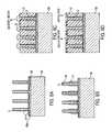
- FIGS. 1A and 1BExamples of prior art three dimensional vertical NAND strings are illustrated in FIGS. 1A and 1B .
- the device shown in FIG. 1Ais known in the art as terabit cell array transistor (“TCAT”) array. It includes damascened metal gate SONOS type cells in the vertical NAND flash string formed by a gate replacement process (see Jang, et al., “Vertical cell array using TCAT (Terabit Cell Array Transistor) technology for ultra high density NAND flash memory,” 2009 Symposium on VLSI Technology Digest of Technical Papers, pages 192-193, Jun. 16, 2009, Honolulu, Hi., incorporated herein by reference in its entirety).
- TCATterabit cell array transistor
- P-BiCSPipe-shaped Bit Cost Scalable
- One embodiment of the inventionincludes a method of making a vertical NAND device includes forming a lower portion of a memory stack over a substrate, forming a lower portion of memory openings in the lower portion of the memory stack, and at least partially filling the lower portion of the memory openings with a sacrificial material.
- the methodalso includes forming an upper portion of the memory stack over the lower portion of the memory stack and over the sacrificial material, forming an upper portion of the memory openings in the upper portion of the memory stack to expose the sacrificial material in the lower portion of the memory openings, removing the sacrificial material to connect the lower portion of the memory openings with a respective upper portion of the memory openings to form continuous memory openings extending through the upper and the lower portions of the memory stack, and forming a semiconductor channel in each continuous memory opening.
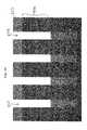
- FIG. 1Ais a side cross sectional views of a prior art NAND memory device.
- FIG. 1Bis a perspective cross sectional view of another prior art NAND memory device.
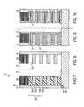
- FIGS. 2A , 2 B, 3 A and 3 Bare side cross sectional views of a NAND memory device of embodiments of the invention.
- FIG. 3Cis a top cross sectional view of the device of FIGS. 3A and 3B .
- FIG. 2Cis a top cross sectional view of NAND memory devices of FIGS. 2A and 2B .
- FIGS. 2D and 2Eare schematic circuit diagrams of the devices of FIGS. 2A and 2B , respectively.
- FIG. 4Ais a side cross sectional views of a NAND memory device of an embodiment of the invention.
- FIG. 4Bis a top cross sectional view of the device of FIG. 4A .
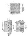
- FIGS. 5A and 5Bare perpendicular side cross sectional views along lines A-A′ and B-B′ in FIG. 5C of a lower select gate device level of the NAND memory device of an embodiment of the invention.
- FIG. 5Cis a top cross sectional view of the device of FIGS. 5A and 5B .
- FIGS. 6A , 6 B, 6 C and 6 Dare side cross sectional views of steps in the method of making the lower select gate device level of the NAND memory device of an embodiment of the invention.
- FIGS. 7 , 8 , 9 and 10are side cross sectional views of steps in the method of making the memory device levels of the NAND memory device of an embodiment of the invention.
- FIGS. 11A and 11Bare perpendicular side cross sectional views along lines A-A′ and B-B′ in FIG. 11C of an upper select gate device level of the NAND memory device of an embodiment of the invention.
- FIG. 11Cis a top cross sectional view of the device of FIGS. 11A and 11B .
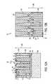
- FIGS. 12A and 12Bare side cross sectional views of respective lower and upper select gate device level of the NAND memory device of an embodiment of the invention.
- FIGS. 13A and 13Bare side cross sectional views of NAND memory devices of other embodiments of the invention.
- FIG. 14Ais a top cross sectional view of the prior art device and FIGS. 14B and 14C are a top cross sectional views of NAND memory devices according to embodiments of the invention.
- FIGS. 14D and 14Eare respective side cross sectional views along lines A-A′ and B-B′ in FIG. 14C of a NAND memory device of an embodiment of the invention.
- FIGS. 15A to 15Hare side cross sectional views of steps in the method of making the NAND memory device shown in FIG. 2A .
- FIGS. 16A to 16Bare side cross sectional views of steps in the method of making the NAND memory device shown in FIG. 3A .
- FIGS. 17A to 17Hare side cross sectional views of steps in the method of making the NAND memory device shown in FIG. 2B .
- FIGS. 18A to 18Gare side cross sectional views of steps in the method of making the NAND memory device according to an embodiment.
- FIGS. 19A to 19Hare side cross sectional views of steps in the method of making the NAND memory device according to an embodiment.
- FIGS. 20A to 20Jare side cross sectional views of steps in the method of making the NAND memory device according to an embodiment.
- FIGS. 21A to 21Fare side cross sectional views of steps in the method of making the NAND memory device according to an embodiment.
- a memory layerincludes a control gate and associated charge storage region (e.g., a dielectric isolated floating gate, an ONO stack, etc.) and at least a portion of two dielectric isolation layers located above and below each control gate.
- the hard mask thickness used during high aspect ratio etchinglimits of the maximum number of stacked memory layers in the VNAND because the amount of hard mask thickness consumed increases during memory opening etching with increasing amount of memory layers stacked in the memory structure. For example, for a 1500 nm thick hard mask, at most 35 memory layers may be etched using reactive ion etching (RIE) to form the memory opening before all of the hard mask thickness is consumed by the etching.
- RIEreactive ion etching
- RIEreactive ion etching
- Increasing the hard mask thickness to increase the number of stacked memory levelsis also not highly desirable because an increase in the hard mask thickness undesirably increases the aspect ratio of the opening.
- RIE energyalso limits the number of stacked memory layers in the VNAND.
- the reactive ionsare scattered within the high aspect memory opening during the etching, which leads to a decrease in the RIE energy.
- the RIE energywill eventually be reduced to an extent at which the RIE process loses the capability to etch the memory opening. Therefore, with a smaller RIE energy, a lower number of memory layers can be etched at the same time.
- increasing the RIE energyis also not highly desirable because it leads to increased back sputtering effects which may lead to control gate to control gate (i.e., word line to word line) shorts. Therefore, the RIE energy also limits the number of stacked memory layers in the VNAND.
- the present inventorsrealized that the number of stacked memory layers in a VNAND may be increased if the portions of each memory openings are etched sequentially. Due to the limited depth of the opening in sequential etching, the high etching aspect etching ratio challenges noted above may be decreased.
- a lower portion of the memory stackis formed over a substrate. This portion includes only a part of the memory layers that will be used in the VNAND.
- the lower portions of the memory openingsare etched in the lower portion of the memory stack.
- at least one additional portion of the memory stackis formed over the lower portion of the memory stack.
- the at least one additional portion of the memory stackcontains additional memory levels.
- additional portions of the memory openingsare then etched in the at least one additional portion of the memory stack.
- the at least one additional portioncomprises an upper portion of the stack and the additional portions of the memory openings comprise upper portions of the memory openings. If the stack contains more than two portions, then the above process may be repeated several times. In this case, the at least one additional portion comprises one or more middle portions and an upper portion of the stack and the additional portions of the memory openings comprise one or more middle portions and upper portions of the memory openings.
- each hard mask used during each etching stepmay be relatively thin and the hard mask thickness does not limit the total number of memory layers in the stack.
- each RIE step of each memory opening portionsforms an opening that has a limited depth, the RIE energy also does not limit the total number of memory layers in the stack.
- each memory openingi.e., lower portion, upper portion and optionally one or more middle portions
- the misalignment of the memory opening portionsmay lead to channel discontinuity which results in an open NAND string.
- the present inventorsrealized that the memory opening alignment challenges may be reduced or avoided by adding a landing pad between the memory stack portions.
- the landing padis wider (e.g., had a larger diameter) than the channel in the horizontal direction.
- the landing padmay be 10-100% wider, such as 25-75% wider than the channel (i.e., for disc shaped pads and cylindrical channels, the pad diameter is larger than the channel diameter by 10-100%).
- the pad diameteri.e., width
- the padmay be 20-50 nm, such as 30-40 nm thick.
- the landing padconnects adjacent channel portions in adjacent memory opening portions of the same memory opening even if the memory opening portions are misaligned with respect to each other.
- the landing padmay comprise any suitable semiconductor or electrical conductor material, such as silicon, metal, metal alloy, etc.
- the landing padis made of the same semiconductor material as the channel of the VNAND.
- the landing padmay comprise a polysilicon landing pad if the channel is a polysilicon channel.
- a semiconductor landing padmay be intrinsic or have the same conductivity type (e.g., p or n) as the channel.
- the semiconductor landing padmay be heavier doped than the channel (e.g., heavily doped landing pad and lightly doped channel), have the same doping concentration as the channel or may be lighter doped than the channel.
- the pad resistivitymay be less than, greater than or the same as the resistivity of the channel material.
- the landing padmay comprise a metal (e.g., Ti, W, etc.) or conductive metal alloys (e.g., TiN, WN, a metal silicide, such as titanium, tungsten, nickel, cobalt or platinum silicide, etc.).
- a metale.g., Ti, W, etc.
- conductive metal alloyse.g., TiN, WN, a metal silicide, such as titanium, tungsten, nickel, cobalt or platinum silicide, etc.
- the landing padmay be formed over each channel portion (except over the upper most channel portion if desired) during the same deposition step as the channel deposition step or during subsequent deposition step. Then, the next overlying channel portion is formed on the landing pad.
- the landing padmay also be considered a resistor built into the vertical channel of the VNAND string.
- the impact of the increase in resistance on the VNAD read performance due to the presence of the resistorshould not be great.
- the resistance valueis 1.35 kOhm. If the stack includes five landing pads per channel or ten landing pads per U-shaped channel in a P-BiCS VNAND, then the total resistance is 13.5 kOhm for a 50 nm diameter memory opening. If a 400 nA read current is used in the NAND string, then the bit line voltage needs to increase by only 5 mV due to the ten additional series resistors/landing pads. Likewise, an additional thermal budget (e.g., MONOS anneal) may be added due to the presence of the landing pads. However, the thermal budget impact on the NAND string characteristics should be manageable.
- MONOS anneale.g., MONOS anneal
- VNAND devices containing a landing pad/built-in resistormay have any suitable configuration.
- FIGS. 2A through 4Billustrate various non-limiting, exemplary VNAND devices containing a landing pad/built-in resistor.
- FIGS. 2A and 2Dillustrate a VNAND containing a landing pad/built-in resistor having a single vertical channel having a “TCAT” type configuration.
- FIGS. 2B and 2Eillustrate a VNAND containing a landing pad/built-in resistor having a U-shaped (e.g., pipe shaped) channel having a “P-BiCS” type configuration.
- FIG. 2Cillustrates a top view of the devices in FIGS. 2A and 2B .
- FIGS. 3A through 4Billustrate a VNAND containing a landing pad/built-in resistor having a compact VNAND (“CVNAND”) type configuration, which will be described in more detail below.
- the CVNAND deviceis also described in more detail in U.S. patent application Ser. No. 13/754,293, filed on Jan. 30, 2013 and incorporated herein by reference in its entirety.
- the NAND string 180 illustrated in FIGS. 2A-4Bmay be formed with a vertical channel.
- the vertical channel 1has a solid, rod shape as shown in FIGS. 2A , 2 B, 3 B, 3 A and 4 B.
- the entire channelcomprises a semiconductor material.
- the vertical channelhas a hollow cylinder shape as shown in FIG. 4A .
- the vertical channelincludes a non-semiconductor core 2 surrounded by a semiconductor channel 1 shell. The core may be unfilled or filled with an insulating material, such as silicon oxide or silicon nitride.
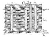
- the monolithic three dimensional NAND string 180comprises a semiconductor channel 1 having at least one end portion extending substantially perpendicular to a major surface 100 a of a substrate 100 , as shown in FIGS. 2A , 2 D, 3 A and 3 B.
- the semiconductor channel 1may have a pillar shape and the entire pillar-shaped semiconductor channel extends substantially perpendicularly to the major surface 100 a of the substrate 100 .
- the source/drain electrodes of the devicecan include a lower electrode 102 (e.g., a heavily doped semiconductor region source electrode in the major surface 100 a of a semiconductor substrate 100 ) provided below the semiconductor channel 1 (optionally in contact with a doped source region 103 ), and an upper electrode 202 (e.g., bit line) formed over the doped drain region 203 in the semiconductor channel 1 , as shown in FIG. 2A .
- the lower electrode 102contacts a metal interconnect outside of the view shown in FIGS. 2A and 3A or contacts metal wires of circuitry under the array.
- the drain/bit line electrode 202contacts the pillar-shaped semiconductor channel 1 (via the drain region 203 ) from above, and the source electrode 102 contacts the pillar-shaped semiconductor channel 1 from below (e.g., via source region 103 ).
- 2A and 2Dcontains two levels of landing pads 25 , which divide the channel and the stack into three portions: lower portion of the stack 120 L containing the lower portions 1 xa , 1 xb of the wings 1 a , 1 b ; middle portion of the stack 120 M containing the middle portions 1 ya , 1 yb of the wings 1 a , 1 b ; and upper portion of the stack 120 U containing the upper portions 1 za , 1 zb of the wings 1 a , 1 b.
- the NAND stringmay have a U shape (also known as a “pipe” shape) with two vertical channel wing portions connected with a horizontal channel connecting the wing portions.
- the U shaped or pipe shaped channelmay be solid, as in the solid rod shaped vertical channel NAND as shown in FIG. 2B .
- the U shaped or pipe shaped channelmay be hollow cylinder shaped, (similar to the hollow cylinder pipe shaped vertical channel NAND as shown in FIG. 4A ).
- the U-shaped pipe channelmay be filled or unfilled.
- the two wing portions 1 a and 1 b of the U-shape semiconductor channelmay extend substantially perpendicular to the major surface of the substrate, and a connecting portion 1 c of the U-shape semiconductor channel 1 connects the two wing portions 1 a , 1 b extends substantially perpendicular to the major surface of the substrate.
- the wing portions 1 a , 1 b of the channel 1contain the built-in landing pads/resistors 25 .
- 2B and 2Econtains two levels of landing pads 25 , which divide the channel and the stack into three portions: lower portion of the stack 120 L containing the lower portions 1 xa , 1 xb of the wings 1 a , 1 b ; middle portion of the stack 120 M containing the middle portions 1 ya , 1 yb of the wings 1 a , 1 b ; and upper portion of the stack 120 U containing the upper portions 1 za , 1 zb of the wings 1 a , 1 b.
- one of the source or drain electrodes 202contacts the first wing portion of the semiconductor channel from above, and another one of a source or drain electrodes (e.g., source line) 102 contacts the second wing portion of the semiconductor channel 1 from above.
- An optional body contact electrode 91may be disposed over or in the substrate to provide body contact to the connecting portion of the semiconductor channel 1 from below.
- the NAND string's select or access transistors 16are shown in FIGS. 2B and 2E . These transistors and their operation are described in U.S. Pat. No. 8,187,936, which is incorporated by reference for a teaching of the select transistors.
- the device of FIGS. 2B and 2Eis described in more detail below with reference to the method of making the P-BiCS type VNAND, as shown in FIGS. 17A-17H .
- the substrate 100can be any semiconducting substrate known in the art, such as monocrystalline silicon, IV-IV compounds such as silicon-germanium or silicon-germanium-carbon, III-V compounds, II-VI compounds, epitaxial layers over such substrates, or any other semiconducting or non-semiconducting material, such as silicon oxide, glass, plastic, metal or ceramic substrate.
- the substrate 100may include integrated circuits fabricated thereon, such as driver circuits for a memory device.
- any suitable semiconductor materialscan be used for semiconductor channel 1 , for example silicon, germanium, silicon germanium, indium antimonide, or other compound semiconductor materials, such as III-V or II-VI semiconductor materials.
- the semiconductor materialmay be amorphous, polycrystalline or single crystal.
- the semiconductor channel materialmay be formed by any suitable deposition methods.
- the semiconductor channel materialis deposited by low pressure chemical vapor deposition (LPCVD).
- LPCVDlow pressure chemical vapor deposition
- the semiconductor channel materialmay be a recyrstallized polycrystalline semiconductor material formed by recrystallizing an initially deposited amorphous semiconductor material.
- the insulating fill material 2 in FIG. 4Amay comprise any electrically insulating material, such as silicon oxide, silicon nitride, silicon oxynitride, or other insulating materials.
- Each monolithic three dimensional NAND string 180further comprises a plurality of control gate electrodes 3 , as shown in FIGS. 2A , 2 B, 3 A, 3 B and 4 A- 4 B.
- the control gate electrodes 3may comprise a portion having a strip shape extending substantially parallel to the major surface 100 a of the substrate 100 .
- the plurality of control gate electrodes 3comprise at least a first control gate electrode 3 a located in a first device level (e.g., device level A) and a second control gate electrode 3 b located in a second device level (e.g., device level B) located over the major surface 100 a of the substrate 100 and below the device level A, as shown in FIGS. 2A , 2 B, 3 A and 4 A.
- the control gate materialmay comprise any one or more suitable conductive or semiconductor control gate material known in the art, such as doped polysilicon or a metal, such as tungsten, copper, aluminum, tantalum, titanium, cobalt, titanium nitride or alloys thereof.
- Each channel 1 shown in FIGS. 2A-4Bcontains one or more landing pads/built-in resistors 25 described above.
- each landing pad 25is located in a vertical position of the channel between control gates 3 (i.e., having one control gate above and one control gate below).
- the landing padis located between the first device level (e.g., level A) and the second device level (e.g., level B).
- a lower portion of the semiconductor channel (e.g., 84 x ) located in the first device levelcontacts a bottom surface of the landing pad 25 .
- a middle or upper portion (e.g., 84 y ) of the semiconductor channel located in the second device levelcontacts a top surface of the same landing pad 25 .
- the landing pad 25may extend horizontally beyond the memory hole 84 diameter or width to be located over and under adjacent control gates 3 inside the dielectric fill material 121 .
- the landing pad 25may extend into the insulating layer 121 between the first 3 a and the second 3 b control gate electrodes 3 .
- the fill material 121isolates the landing pad 25 from direct contact with the control gate electrodes 3 .
- the landing pad 25may be relatively thick and contact dummy control gate electrodes 3 d , as shown in FIGS. 17G and 17H .
- Dummy control gate electrodes 3 di.e., dummy word lines
- a blocking dielectric 7is located adjacent to and may be surrounded by the control gate(s) 3 .
- the blocking dielectric 7may comprise a continuous layer or a plurality of blocking dielectric segments located in contact with a respective one of the plurality of control gate electrodes 3 .
- a first dielectric segment 7 a located in device level A and a second dielectric segment 7 b located in device level Bare in contact with control electrodes 3 a and 3 b , respectively, as shown in FIG. 4A .
- at least a portion of each of the plurality of blocking dielectric segments 7surrounds the top, bottom, and two edge portions of a control gate electrode 3 between two adjacent NAND strings, as shown in FIGS. 3A and 4A .
- the NAND devicesalso comprise one or more charge storage regions 9 located between the channel 1 and the blocking dielectric 7 .
- the charge storage regions 9may comprise a continuous vertical charge storage layer adjacent to plural control gate electrodes 3 , as shown in FIGS. 2A and 2B or the plurality of discrete charge storage regions 9 comprise at least a first discrete charge storage segment 9 a located in the device level A and a second discrete charge storage segment 9 b located in the device level B, as shown in FIG. 4A .
- a tunnel dielectric 11is located between the charge storage region(s) 9 and the semiconductor channel 1 .
- the blocking dielectric 7 and the tunnel dielectric 11may be independently selected from any one or more same or different electrically insulating materials, such as silicon oxide, silicon nitride, silicon oxynitride, or other insulating materials.
- the charge storage region(s) 9may comprise a conductive (e.g., metal or metal alloy such as titanium, platinum, ruthenium, titanium nitride, hafnium nitride, tantalum nitride, zirconium nitride, or a metal silicide such as titanium silicide, nickel silicide, cobalt silicide, or a combination thereof) or semiconductor (e.g., polysilicon) floating gate(s), conductive nanoparticles, or a charge storage dielectric layer or segment (e.g., silicon nitride or another dielectric).
- a conductivee.g., metal or metal alloy such as titanium, platinum, ruthenium, titanium nitride, hafnium nitride, tantalum nitride, zirconium nitride, or a metal silicide such as titanium silicide, nickel silicide, cobalt silicide, or a combination thereof
- semiconductore.
- the charge storage regionscomprise silicon nitride, where the silicon oxide blocking dielectric 7 , the nitride charge storage region 9 and the silicon oxide tunnel dielectric 11 form oxide-nitride-oxide (ONO) memory film 13 of the NAND string shown in FIGS. 2A , 2 B, 3 A and 4 A.
- the blocking dielectricmay comprises a tri-layer ONO dielectric, such that the memory film 13 comprises ONO (11) —N (9) —O (7).
- the tunnel dielectric 11comprises a cylinder which surrounds the semiconductor channel 1
- the charge storage region 9comprises a cylinder which surrounds the tunnel dielectric
- the blocking dielectric 7comprises a cylinder which surrounds the charge storage region.
- the first 3 a and the second 3 b control gate electrodes 3surround the blocking dielectric in each NAND string.
- each TCAT NAND string 180is separated from adjacent strings by a word line cut or trench 86 .
- the bottom source select gate (SGS) device 16 L in TCATrequires a cut space or trench 86 between the lower select gate electrodes which are built from the bottom of the stack metal layer.
- the source line 102 formation process and p-well 300 contactrequires additional space in the TCAT device.
- each U-shaped P-BiCS NAND string 180contains a dielectric 87 filled slit trench 86 A between the select gates 3 and the wings or arms of the U-shaped channel 1 which extends between upper source line 102 and bit line 202 .
- adjacent U-shaped NAND strings 180are also separated by a word line cut or trench 86 B not to lose active holes and to reduce word line R s .
- the top view of the filled memory holes 84i.e., containing the NAND string channels 1 and a film 13 comprising tunnel dielectric, charge storage region and blocking dielectric
- the trenches 86 in TCAT and P-BiCS devicesis illustrated in FIG. 2C .
- control gatesare omitted from FIG. 2C for clarity and the supporting columns 88 which prevent the device levels from collapsing on each other during removal of sacrificial material are shown in the bottom of the figure.
- the trenchesresult in a higher than desired pitch between adjacent filled memory holes (e.g., a pitch of about 150 nm) and reduces the array efficiency by more than 50%.
- the word line (i.e., control gate) trenches or cuts 86 in an array of vertical NAND stringsmay be eliminated to increase the device density and reduce the filled memory hole 84 pitch.
- Embodimentsinclude monolithic three dimensional NAND strings and methods of making three dimensional NAND devices (e.g., CVNAND devices) having at least one 3 ⁇ 3 array of vertical NAND strings in which the control gate electrodes are continuous in the array and do not have an air gap or a dielectric filled trench 86 in the array.
- the NAND deviceis formed by first forming a lower select gate level having separated lower select gates, then forming plural memory device levels containing a plurality of NAND string portions, and then forming an upper select gate level over the memory device levels having separated upper select gates.
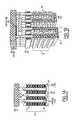
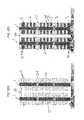
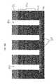
- FIGS. 3A , 3 B, 3 C, 4 A and 4 BEmbodiments of the compact vertical NAND (i.e., CVNAND) device are shown in FIGS. 3A , 3 B, 3 C, 4 A and 4 B.
- FIG. 3Aschematically illustrates a side cross sectional view of the entire CVNAND device, including the lower 50 and upper 60 select gate device levels located below and above the memory device levels 70 shown in FIG. 4A .
- FIG. 3Bschematically illustrates a side cross sectional view of the memory levels 70 and select gate device levels 50 , 60 of one CVNAND array
- FIG. 3Cschematically illustrates the top view location of the filled memory holes 84 and supporting pillars 88 .
- FIG. 3Aschematically illustrates a side cross sectional view of the entire CVNAND device, including the lower 50 and upper 60 select gate device levels located below and above the memory device levels 70 shown in FIG. 4A .
- FIG. 3Bschematically illustrates a side cross sectional view of the memory
- FIG. 4Aillustrates a side cross sectional view of the memory device levels 70 (i.e., levels containing the control gate electrodes/word lines) in one NAND string array.
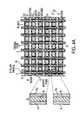
- FIG. 4Bschematically illustrates the top cross sectional view of the relationship between the continuous control gate electrodes 3 and the filled memory holes 84 in each array block.
- the first control gate electrode 3 a and the second control gate electrode 3 bare continuous in the array, such that these electrodes do not have an air gap or a dielectric filled trench in the array.
- the control gate electrodes 3 when viewed from the topcomprise a “mesh” which is continuous except for the memory holes 84 which are completed filled with the channel 1 , an optionally the tunnel dielectric 11 , charge storage region 9 , blocking dielectric 7 and optional insulating fill 2 .
- the control gate electrodes 3may be considered to be a mesh in which all openings are filled
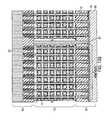
- FIG. 4Bshows two control gate electrodes 3 a L and 3 a R (i.e., left and right electrodes) located in the first device level A. Each electrode forms a continuous mesh around an exemplary 4 ⁇ 3 array of filled memory holes 84 . Each electrode 3 a L and 3 a R contacts a respective word line 200 L and 200 R of an array block.
- An array blockincludes plural arrays (e.g., plural 4 ⁇ 3 arrays) which are connected by their respective control gate electrodes (e.g., 3 a L) to a common word line (e.g., 200 L). Only one array is shown as being connected to each word line via a respective control gate electrode in FIG. 4B for clarity. However, it should be understood that the pattern shown in FIG.
- each arrayis located in a respective array block, where the left control gate electrode 3 a L in one block in device level A is separated from the right control gate electrode 3 a R in the same level A in an adjacent array block by an air gap (if the slit trench 81 is not filled) or a dielectric filled trench 81 .
- the same configurationis used in the other memory levels shown in FIGS. 4A and 3A .
- the CVNAND string's select or access transistors 16 L, 16 Uare shown in FIGS. 3A , 3 B, 5 , 6 and 11 .
- a lower select gate electrode 51is located adjacent to a lower portion 1 L of the pillar-shaped semiconductor channel 1 below the control gate electrodes 3 (e.g., 3 a , 3 b ) in the lower select gate electrode level 50 .
- Level 50may be a source select gate level and electrode 51 may be a source side select gate electrode.
- Each lower select gate electrode 51is separated from adjacent lower select gate electrodes 51 in the array in level 50 by an air gap or a dielectric filled trench 53 .
- an upper select gate electrode 61is located adjacent to an upper portion 1 U of the pillar-shaped semiconductor channel 1 above the first 3 a and the second 3 b control gate electrodes. Electrode 61 may comprise a drain side select gate electrode located in the drain upper select gate level 60 . Each upper select gate electrode 61 is separated from adjacent upper select gate electrodes 61 in the array in level 60 by an air gap or a dielectric filled trench 63 .
- each semiconductor channel 1comprises a first portion 1 U adjacent to the upper select gate electrode 61 , a second portion 1 L adjacent to the lower select gate electrode 51 , a third (i.e., middle or memory) portion 1 M located at least in the first (A) and the second (B) device levels between the first and the second portions, and an optional, additional landing pad portion 55 located between the second 1 L and the third 1 M channel 1 portions.
- the third (middle) portion 1 M of the channel 1has a larger diameter or width than the first (upper) 1 U and the second (lower) 1 L channel 1 portions because these three portions are formed in separate process steps as described below.
- the thinner upper 1 U and lower 1 L channel 1 portionsallow the space for the air gap or a dielectric filled trench 53 , 63 to be added between adjacent upper 61 and lower 51 select gates in respective levels 60 and 50 .
- the control gates 3are continuous and do not require air gap or trench adjacent to the middle (memory) portions 1 M of the channel 1 , the channel portions 1 M may be thicker than channel portions 1 U and 1 L.
- the channel 1may optionally contain additional landing pad portions 55 between the lower select gate level 50 and the memory levels 70 and between the memory level 70 and the upper select gate level 60 .
- the landing pad portionhas a larger diameter or width than the second 1 L and the third 1 M portions of the channel 1 .
- FIGS. 5A-5Cillustrate a lower select gate level 50 of the CVNAND device.
- FIG. 5Cshows a top view and FIGS. 5A and 5B illustrate side cross sectional views along lines A-A′ and B-B′ in FIG. 5C .
- the lower select gate level 50is located over the substrate 100 .
- the lower select gate level 50includes the lower portions 1 L of the plurality of semiconductor channels 1 (containing source regions 103 on the bottom), and a plurality of lower source electrodes 102 . Each lower source electrode is electrically connected to each of the plurality of lower portions 1 L of the semiconductor channels through a respective source region 103 .
- Level 50also includes the plurality of lower select gate electrodes 51 , located adjacent to a gate dielectric 54 contacting the lower portion 1 L of each semiconductor channel 1 .
- the channel 1 L, gate dielectric 54 and select gate 51form the lower (source) select transistor 16 L of each NAND string.
- Strip shaped lower select gate lines 52connect the select gates 51 in rows to input/outputs (not shown), as shown in FIGS. 5B and 5C .
- Level 50is formed before the layers of the memory level 70 are formed over level 50 to allow the select gates 50 to be separated.
- FIGS. 6A-6Dillustrate steps in forming this level 50 shown in FIG. 5A .
- the lower portions 1 L of the channel 1may be formed by etching a silicon substrate 100 to form silicon pillars 1 L using any suitable lithography and etching technique.
- pillars 1 Lmay be grown in openings in a mask located over the substrate 100 .
- the select gate device level 50is lifted up over the substrate 100 surface 100 a , so that the select transistors 16 L have polysilicon channels 1 L and CMOS devices may be formed in single crystal silicon substrate 100 under the NAND array. This option is less preferred.
- the gate dielectric 54may be deposited on the pillars 1 L and the surface 100 A of the substrate 100 by CVD or other suitable methods.
- the dielectric 54may comprise materials other than silicon oxide.
- the upper surface 100 A of the substrate 100is doped (e.g., by ion implantation) to form the source regions 103 and the source electrode 102 (i.e., buried doped source line in substrate 100 ).
- the buried source line 102 in the substrate 100is made by a high dose implant.
- an optional a buried metal meshe.g., tungsten, etc.
- Source regions 103may be formed by angled ion implantation (e.g., phosphorus or arsenic implant into a p-type silicon substrate) into the base of the pillars 1 L. The implantation may be conducted before or after the dielectric 54 formation or after the select gate 51 formation as it is described below.
- each lower select gate electrode 51is separated from adjacent lower select gate electrodes in the array by an air gap or a dielectric filled trench 53 .
- Thismay be done by forming the select gate 51 layer over the dielectric 54 covered lower portions 1 L of the channel 1 followed by anisotripically etching the select gate layer to leave discreet, separated sidewall spacer shaped select gates 51 on the gate dielectric 54 covered lower portions 1 L of the channel.
- the space between the spacer gates 51may be left as an air gap or filled with an dielectric fill 53 .
- select gates 51may be formed by depositing a conductive layer and patterning it by lithography and etching into discreet gates 51 . If desired, portions of the gates 51 of transistors 16 L may be silicided.
- the select gate lines 52are then formed to connect the discreet select gates into rows.
- the lines 52may be formed by depositing one or more conductive layers and then performing lithography and etching to form the strip shaped lines 52 .
- the lines 52are separated from each other in the A-A direction but not in the B-B direction in FIG. 5C .
- the optional semiconductor landing pad 55may epitaxially grown over each lower portion 1 L of the plurality of semiconductor channels 1 exposed in the dielectric filled trenches 53 in the lower select gate level 50 , such that the landing pad has a larger width or diameter than an underlying lower portion of the channel.
- the landing pad 55 formationmay comprise epitaxially growing a “mushroom head” shaped overgrown silicon 56 on exposed portions 1 L of the channels 1 .
- This silicon overgrowth 56is then covered by an insulating gap fill layer (e.g., silicon oxide or nitride).
- the silicon mushroom head 56 and the gap fill layerare then planarized (e.g., by CMP) to form planar landing pads 55 on each pillar 1 L separated by an insulating gap fill 57 , as shown in FIG. 6D .
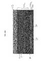
- FIGS. 7-10illustrate a method of making the lower portion of the memory device levels 70 of FIGS. 4A and 3A after the step of forming a lower select gate level 50 according to an embodiment of the invention.
- the memory device levels 70comprise a plurality of NAND string portions.
- a stack 120 of alternating layers 121 ( 121 a , 121 b , etc.) and 132 ( 132 a , 132 b etc.)is formed over the completed lower select gate device level 50 which is located over major surface of the substrate 100 .
- Layers 121 , 132may be deposited over the substrate by any suitable deposition method, such as sputtering, CVD, PECVD, MBE, etc.
- the layers 121 , 132may be 6 to 100 nm thick.
- the stack 120may be covered with an optional cap layer of insulating material 200 different from materials 121 and 132 .
- the first layers 121comprise an electrically insulating material, such as silicon oxide, silicon nitride, high-k dielectric (e.g., organic or inorganic metal oxide), etc.
- the second layers 132are sacrificial layers. Any sacrificial material that can be selectively etched compared to material 121 may be used for layers 132 , such as conductive or insulating or semiconducting material.
- the sacrificial material for layers 132may be silicon nitride when material of layers 121 is silicon oxide.
- the deposition of layers 121 , 132is followed by etching the stack 120 to form a plurality of memory holes 84 .
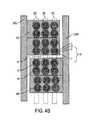
- An at least a 3 ⁇ 3, such as an at least 6 ⁇ 6 array of memory holes 84may be formed in locations where vertical channels of NAND strings will be subsequently formed.
- the middle semiconductor channel 1 portions 1 Mare then formed on the landing pads 55 exposed in the memory holes 84 .
- the channel portions 1 Mmay be filled with insulating fill 2 (as shown in FIG. 4A ) or may comprise a solid rod (as shown in FIGS. 3A and 7 ).
- the channel 1 portions 1 M materialcomprises lightly doped p-type or n-type (i.e., doping below 10 17 cm ⁇ 3 ) silicon material (e.g., polysilicon).
- An n-channel deviceis preferred since it is easily connected with n+ junctions (i.e., source 103 and drain 203 n+ doped regions having a doping concentration between 10 17 cm ⁇ 3 and 10 21 cm ⁇ 3 ).
- a p-channel devicemay also be used.
- Other semiconductor materialse.g., SiGe, SiC, Ge, III-V, II-VI, etc. may also be used.
- the semiconductor channel 1may be formed by any desired methods.
- the semiconductor channel material 1may be formed by depositing semiconductor (e.g., polysilicon) material in the holes 84 and over the stack 120 (e.g., by CVD), followed by a step of removing the upper portion of the deposited semiconductor layer by chemical mechanical polishing (CMP) or etchback using top surface of the stack 120 as a polish stop or etch stop.
- semiconductore.g., polysilicon
- CVDchemical mechanical polishing
- a single crystal silicon or polysilicon vertical channel 1may be formed by metal induced crystallization (“MIC”, also referred to as metal induced lateral crystallization) without a separate masking step.
- MICmetal induced crystallization
- the MIC methodprovides full channel crystallization due to lateral confinement of the channel material in the hole 84 .
- an amorphous or small grain polysilicon semiconductor (e.g., silicon) layercan be first formed in the holes 84 and over the stack 120 , followed by forming a nucleation promoter layer over the semiconductor layer.
- the nucleation promoter layermay be a continuous layer or a plurality of discontinuous regions.
- the nucleation promoter layermay comprise any desired polysilicon nucleation promoter materials, for example but not limited to nucleation promoter materials such as Ge, Ni, Pd, Al or a combination thereof.
- the amorphous or small grain semiconductor layercan then be converted to a large grain polycrystalline or single crystalline semiconductor layer by recrystallizing the amorphous or small grain polycrystalline semiconductor.
- the recrystallizationmay be conducted by a low temperature (e.g., 300 to 600 C) anneal.
- the upper portion of the polycrystalline semiconductor layer and the nucleation promoter layercan then be removed by CMP or etchback using top surface of the stack 120 as a stop, resulting in the structure as shown in FIG. 7 .
- the removalmay be conducted by selectively wet etching the remaining nucleation promoter layer and any formed silicide in the top of layer following by CMP of the top of silicon layer using the top of the stack 120 as a stop.
- At least one slit trench 81is formed in the stack 120 .
- the openings 81 , 84may be formed by forming a mask (e.g., a photoresist mask) by photolithography followed by etching unmasked areas.
- the slit trench opening 81may be in the shape of a cut traversing more than one NAND string as illustrated in FIG. 4B .
- the slit trenches 81allow back side access to the vertical NAND strings located in memory holes 84 for the control gate 3 formation in the “gate last” process.
- the sacrificial material 132is selectively etched compared to the first layer 121 material to form recesses 62 .
- the recesses 62may be formed by selective, isotropic wet or dry etching which selectively etches the sacrificial material 132 compared to the first layer insulating material 121 through the slit trenches 81 .
- the recess 62extends to the channel 1 portions 1 M.
- the entire layers of first sacrificial material 132 between the first layers 121are removed up to the channel 1 portions 1 M.
- the memory film 13is then formed in the recesses 62 as shown in FIG. 9 .
- Thisincludes forming a tunnel dielectric 11 in the recesses over the channel portions 1 M located in the memory openings 84 , forming a charge storage region 9 over the tunnel dielectric, and forming a blocking dielectric 7 over the charge storage region in the recesses 62 .
- the blocking dielectric 7may comprise a silicon oxide layer deposited by conformal atomic layer deposition (ALD) or chemical vapor deposition (CVD). Other high-k dielectric materials, such as hafnium oxide, may be used instead or in addition to silicon oxide. Dielectric 7 may have a thickness of 6 to 20 nm.
- the charge storage region 9may comprise a silicon nitride layer deposited by any suitable method, such as ALD, CVD, etc., and have a thickness of 3 to 20 nm.
- the tunnel dielectricmay comprise a relatively thin insulating layer (e.g., 4 to 10 nm thick) of silicon oxide or other suitable material, such as oxynitride, oxide and nitride multi layer stacks, or a high-k dielectric (e.g., hafnium oxide).
- the tunnel dielectricmay be deposited by any suitable method, such as ALD, CVD, etc. Alternatively, the tunnel dielectric may be formed by thermally oxidizing the exposed sidewalls of the middle portions 1 M of the channel 1 exposed in the recesses 62 .
- control gates 3are then formed on the blocking dielectric in the remaining portions of the recesses 62 through the slit trench(es) 81 , as shown in FIG. 10 .
- the control gates 3are preferably metal or metal alloy gates, such as tungsten gates, formed by MOCVD or other suitable methods.
- the slit trenches 81 between array blocksmay be filled with a dielectric fill material or they may be left unfilled as air gap trenches. This completes the lower portion of the memory device levels 70 .
- FIGS. 7-10is repeated again one or more times to form one or more upper portions of the memory levels 70 over the completed lower portion of the memory levels 70 , as shown in FIG. 16B , and described in more detail below.
- FIGS. 11A-11Cillustrate the upper select gate level 60 of the device.
- FIG. 11Cshows a top cross sectional view (along lines A-A and B-B in FIGS. 11A and 11B , respectively, with bit line 202 not shown) and FIGS. 11A and 11B illustrate side cross sectional views along lines A-A′ and B-B′ in FIG. 11C .
- the upper select gate level 60is formed over the plurality of memory device levels 70 , preferably after levels 70 are completed and preferably without using the stack 120 layers.
- the upper select gate level 60comprises upper portions 1 U of the plurality of semiconductor channels 1 , and a plurality of upper drain electrodes (e.g., bit lines) 202 .
- Each upper source or drain electrode 202is electrically connected to each of the plurality of upper portions 1 U of the semiconductor channels via the drain regions 203 .
- Level 60also includes a plurality of upper select gate electrodes 61 .
- Each upper select gate electrode 61is located adjacent to a gate dielectric 64 contacting the upper portion 1 U of each semiconductor channel 1 .
- the channel portion 1 U, gate dielectric 64 and select gate 61form the upper (drain) select transistor 16 U of each NAND string.
- the upper select gate lines 66 separated from each other by insulating fill 63connect the select gates 61 in rows.
- the upper select gate level 60may be formed in the same manner as the lower select gate level 50 , except as follows. First, the upper portions 1 U (i.e., the channels of the upper select gate transistors 16 U) of the channels 1 are grown on the respective middle portions 1 M of the channels. Thus, portion 1 U may comprise polycrystalline semiconductor (e.g., polysilicon) or recrystallized, nearly single crystal silicon (e.g., recrystallized by the MIC process).
- polycrystalline semiconductore.g., polysilicon
- recrystallized, nearly single crystal silicone.g., recrystallized by the MIC process.
- the tops of the pillars 1 Uare doped with a dopant of the opposite conductivity type (e.g., n-type) than that of the channel 1 portion 1 U (e.g., p-type) to form drain regions 203 .
- a dopant of the opposite conductivity typee.g., n-type
- the bit lines 202are formed by a damascene process in rail shaped trenches in a dielectric layer 204 or by forming the dielectric layer 204 around bit line 202 rails.
- the upper select gate electrodes 61may be formed by a sidewall spacer process on gate dielectric 64 covered silicon channels 1 L of the upper select gate transistors 16 U in the same matter as the lower select gate electrodes 51 . If desired, portions of the gates 61 and/or the drain 203 of transistors 16 U may be silicided.
- FIGS. 12A and 12Billustrate exemplary dimensions (in nanometers) of the select transistors 16 and elements of levels 50 and 60 , respectively, in units of nanometers.
- the above configurationprovides a dense array for larger block sizes.
- the CVNANDscales below 5 nm effective half pitch (F/n), where F is the minimum feature size and n is the number of device levels.
- the above described NAND devicemay be programmed and read by conventional NAND techniques. However, since the select gates for each NAND string are separated, the erase operation of the above device may be advantageously performed by a gate induced drain leakage (GIDL) process through the lower select gate source transistor 16 L in the lower select gate device level 50 .
- GIDLgate induced drain leakage
- the effective GIDL eraseallows erasing of very tall stacks by optimizing the bottom SGS transistor 16 L with respect to GIDL current (during erase) and off/leakage currents (during inhibit). This also provides an effective erase from source line 102 side only, which allows optimization of off current and leakage current (during inhibit and read) for top SGD transistor 16 U. This allows the device to open up an inhibit window and reduce read current leakage for non selected blocks. It is believed that sub block erase could become effective compared to prior art three dimensional NAND.
- FIGS. 13A and 13Bare side cross sectional views of a NAND memory device of embodiments of the invention.
- the devices shown in FIGS. 13A and 13Bare similar to the device shown in FIG. 3A above, except that the devices shown in FIGS. 13A and 13B contain a local interconnect (source contact) 302 .
- the local interconnect 302may extend below the array in the embodiment of FIG. 13A (e.g., the local interconnect may extend in and out of the page under the array in the view of FIG. 13A ). Alternatively, the local interconnect 302 may extend in the slit trenches 81 in the embodiment of FIG. 13B .
- the local interconnect 302may comprise any suitable conductive material, such as tungsten, aluminum, copper, etc.
- the local interconnect 302comprises a vertical pillar which electrically contacts the lower electrode 102 (e.g., the heavily doped semiconductor region source electrode in the major surface of the semiconductor substrate 100 or another electrode located over the substrate).
- the upper portion of the local interconnect 302is in electrical contact with a source line.
- the slit trenches 81 and the local interconnect 302extend through the memory device levels 70 and through the dielectric trench fill material 53 to an exposed upper surface of the lower electrode 102 .
- the sidewalls of the slit trenches 81are coated with an insulating layer 304 , such as silicon oxide (see FIGS. 14D and 14E ), and the local interconnect is formed in the middle of the slit trenches 81 between the insulating layer 304 portions.
- the width of the array of vertical NAND stringsis defined by the space between adjacent trenches 81 , at least one or more of which can be filled with the local interconnect 302 .
- the local interconnect 302may contact a common lower electrode 102 of adjacent arrays of strings to provide source side erase for the strings in plural arrays of NAND strings at the same time.
- the local interconnectmay be formed by etching the trenches 81 as described above all the way to the lower electrode 102 , forming the insulating layer 304 in the trenches 81 and filling the remaining central space in the trenches with the conductive material of the local interconnect 302 .
- the portions of the conductive layer of the local interconnect 302 and/or insulating layer 304 which extends out of the trenches 81may be removed by planarization, such as CMP.
- the local interconnectis formed under the array prior to formation of the array.
- FIG. 14Ais a top cross sectional view of the prior art BiCS NAND device shown in FIGS. 1B and 2B .
- FIGS. 14B and 14Care a top cross sectional views of the CVNAND memory devices according to embodiments of the invention.
- the filled memory holes 84are arranged in a square or rectangular layout with the memory holes located at corners of an imaginary rectangle or square, similar to the BiCS layout in FIG. 14A .
- the upper select gates 61 , bit lines 202 and local interconnect 302 extending to the lower electrode 102are also shown in FIG. 14B .
- FIG. 14Cillustrates an alternative embodiment in which the filled memory holes 84 (i.e., the NAND string channel 1 and memory film 13 ) are arranged in a substantially hexagonal pattern.
- This patterncomprises a repeating unit pattern of seven filled memory holes 84 having a central hole 84 surrounded by six other holes 84 arranged in a hexagonal layout around the central hole 84 .
- a central semiconductor channel 1 and memory film 13 unitis surrounded by six other semiconductor channel and memory film units arranged in a hexagonal layout around the central semiconductor channel and memory film unit.
- the hexagonal patternhas three axes of symmetry, in the same plane, about a point the array. The three axes are separated by substantially 60 degrees from one another.
- the memory holes 84are arranged on a hexagonal grid which is also known as hexagonal tiling, bitruncated hexagonal tiling, or omnitruncated hexagonal tiling.
- hexagonal packing of thetakes only about 87% of the area typically used by the same number of cells using standard rectangular layout shown in FIG. 14A .
- the memory holes 84 in the hexagonally tiled configuration of FIG. 14Care staggered along each select gate 51 , 61 when viewed from the top.
- the hexagonally tiled configuration of FIG. 14Cprovides a relaxed layout (i.e., larger pitch) for the select gates 51 , 61 compared to the layout of FIGS. 14A and 14B .
- the density of the array with the hexagonally tiled configuration of FIG. 14Ccan be increased compared to the layout of FIGS. 14A and 14B , with the bit line 202 pitch reduced by a factor of 2 compared to the one in the layout of FIGS. 14A and 14B .
- FIGS. 14D and 14Eare respective side cross sectional views along lines A-A′ and B-B′ in FIG. 14C of the CVNAND memory device with the hexagonally tiled memory hole 84 configuration.
- Line A-A′is a diagonal line through filled memory holes 84 located on bit lines 1, 3, 4 and 5.
- Line B-Bis a line along bit line 5.
- Arrays having a configuration other than 6 ⁇ 3may also be used as desired.
- FIGS. 14D and 14Ealso illustrate the connector lines 351 , 361 for the respective lower select gates 51 and upper select gates 61 of the respective SGS 16 L and SGD 16 U select transistors.
- the lines 351 , 361may comprise any suitable conductor, such as tungsten, and may connect the select gates to the driver/control circuits (not shown).
- each memory hole 84is labeled d1 and the distance between adjacent memory holes 84 (along the diagonal line A-A′ in FIG. 14C ) is labeled d2.
- the distance between adjacent memory holes 84is ⁇ 3*(d1+d2) ⁇ d1.
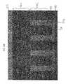
- FIGS. 15A to 15Hare schematic side cross sectional views of steps in the method of making the TCAT type NAND memory device with one or more landing pads 25 shown in FIG. 2A .
- a lower portion of the channel 1is formed in the respective lower portion of the memory opening 84 in the lower portion of the stack.
- Thisis followed by forming the landing pad 25 , forming at least one additional portion of the stack, forming at least one additional portion of the memory opening to expose the landing pad 25 and forming at least one additional portion of the channel 1 in the memory opening in contact with the landing pad 25 .
- the methodbegins by forming the lower electrode 102 , such as by implanting a heavily doped diffusion region 102 in the upper surface 100 a of the substrate 100 .
- region 102may comprise an n+ doped region in a p-type substrate 100 , as shown in FIG. 15A .
- the conductivity typesmay be reversed if desired.
- Diffusion (doped) region 102serves as a common source line of the lower select gate transistor 16 L.
- the lower portion of the memory stack 120 Lis then formed over the upper surface 100 a of the substrate 100 .
- the stackcontains alternating insulating layers 121 , such as silicon oxide layers, and sacrificial layers 132 , such as silicon nitride layers.
- a hard mask 27is formed over the lower portion of the stack.
- the hard maskis patterned (e.g., by lithography) and is used as a mask to etch the lower portions of the memory openings 84 x in the lower portion of the stack 120 L.
- the etchingmay comprise an RIE or another suitable etching.
- the hard mask 27may then be removed or retained in the device. Alternatively, the hard mask is consumed during the etching process.
- the lower portion of the channels 1 xare formed in the lower portion of the memory openings 84 x , as shown in FIG. 15B .
- Any suitable formation methodmay be used, such as the method described above with respect to FIGS. 7-10 .
- the landing pad 25is then formed on top of the lower portion of the channel 1 x , as shown in FIG. 15C .
- the landing pad 25may be formed using any suitable method, such as the method described above for forming the additional landing pad 55 with respect to FIGS. 6C-6D .
- a semiconductor landing pad 25may be epitaxially grown over the each lower portion of the channels 1 x exposed in the lower portion of the stack 120 L, such that the landing pad has a larger width or diameter than an underlying lower portion of the channel 1 x .
- the landing pad 25 formationmay comprise epitaxially growing a “mushroom head” shaped overgrown silicon on exposed lower portions of the channels lx. This silicon overgrowth is then covered by an insulating gap fill layer (e.g., silicon oxide or nitride).
- the silicon mushroom head and the gap fill layerare then planarized (e.g., by CMP) to form planar landing pads 25 on each portion of the channel 1 x separated by an insulating gap fill 521 , as shown in FIG. 15C .
- the landing pads 25may be formed by depositing a conductive or semiconductor layer over the lower portion of the stack 120 L and then patterning the layer by lithography and etching to leave landing pads 25 having a larger width than that of the lower channel portion lx.
- a lower portion of the word line cut or trench 86 xmay then be formed in the lower portion of the stack 120 L.
- This cut or trench 86 xmay be formed by photolithography and etching.
- the cut or trench 86 xmay be filled with a sacrificial or insulating material to protect it during subsequent processing.
- the portion of the cut or trench 86 xis omitted and the entire cut or trench 86 is formed in a single etching step after all of the memory levels are completed. This completes the lower memory level of the NAND device.
- the above processmay be repeated one or more times to form one or more additional memory levels over the lower memory level.
- FIG. 15Dthe process of FIGS. 15A-15C is repeated for the middle portion of the stack 120 M. Specifically, the middle portion of the stack 120 M is formed over the landing pads 25 and the lower portion of the stack 120 L containing the lower portions of the channels 1 x . Another hard mask is formed over the middle portion of the stack 120 M, and the middle portions of the memory openings 84 y are etched into the middle portion of the stack 120 M to expose the landing pads 25 , as shown in FIG. 15D . It should be noted that the lower 84 x and middle 84 y portions of each memory opening 84 may be partially or completely misaligned with each other, as long the landing pads 25 are exposed in respective middle portions of the memory openings 84 y.
- the middle portion of the channels 1 yare formed in the middle portions of the memory openings 84 y , as shown in FIG. 15D .
- the landing pad 25is then formed on top of the middle portion of the channel 1 y .
- the landing pad 25may be formed using any suitable method, such as the method described above.
- a middle portion of the word line cut or trench 86 ymay then be formed in the middle portion of the stack 120 M. This cut or trench 86 y may be formed by photolithography and etching, and optionally filled with a sacrificial or insulating material. This completes the middle memory levels.
- one or more additional middle or upper portions of the memory levelsare then formed over the middle memory levels.
- FIG. 15Ethe process of FIGS. 15A-15C is repeated for the upper portion of the stack 120 U. Specifically, the upper portion of the stack 120 U is formed over the landing pads 25 and the middle portion of the stack 120 M containing the middle portions of the channels 1 y . Another hard mask is formed over the upper portion of the stack 120 U, and the upper portions of the memory openings 84 z are etched into the upper portion of the stack 120 U to expose the landing pads 25 , as shown in FIG. 15E . It should be noted that the middle 84 y and upper 84 z portions of each memory opening 84 may be partially or completely misaligned with each other, as long the landing pads 25 are exposed in respective upper portions of the memory openings 84 z.
- the upper portion of the channels 1 zare formed in the upper portions of the memory openings 84 z , as shown in FIG. 15F .
- the landing pad 25is then formed on top of the upper portion of the channel 1 z .
- the landing pad 25may be formed using any suitable method, such as the method described above.
- the upper select transistor 16 Umay also be formed during this step or during a separate step.
- An upper portion of the word line cut or trench 86 zis then formed in the upper portion of the stack 120 U.
- This cut or trench 86 zmay be formed by photolithography and etching. If the cut or trench portions 86 x , 86 y were filled with a sacrificial material, then the sacrificial material is removed at this time and the cut or trench may be subsequently refilled with an insulating material. Alternatively, the entire cut or trench 86 is formed in a single etching step at this time through the entire stack 120 .
- the memory films and the control gate electrodesare then formed in the entire stack 120 using a back side process (similar to the process shown in FIGS. 8-10 ).
- the sacrificial material layers 132such as the silicon nitride layers
- the memory film 13is then formed on the surface of the recesses 62 through the cut or opening 86 , as shown in FIG. 150 .
- the control gate electrodes 3are then formed in the recesses 62 on the memory films 13 through the cut or opening 86 , as shown in FIG. 15H .
- the back side process shown in FIGS. 15F-15His performed on each portion of the stack between the channel and landing pad formation steps rather than on the entire stack.
- the cut or trench 86 xis formed in the lower portion of the stack 120 L and sacrificial material layers 132 are removed to leave recesses 62 .
- the recessesare then filled with the memory films 13 and the control gate electrodes 3 .
- the cut or trench 86 xmay be filled with an insulating or sacrificial material and the landing pads 25 are then formed on the lower portion of the channels lx.
- the processthen continues as shown in FIG. 15D .
- the cut or trench 86 yis formed in the middle portion of the stack 120 M and sacrificial material layers 132 are removed to leave recesses 62 .
- the recessesare then filled with the memory films 13 and the control gate electrodes 3 .
- the cut or trench 86 ymay be filled with an insulating or sacrificial material and the landing pads 25 are then formed on the middle portion of the channels 1 y .
- the processthen continues as shown in FIG. 15E .
- the cut or trench 86 zis formed in the upper portion of the stack 120 L and sacrificial material layers 132 are removed to leave recesses 62 .
- the recessesare then filled with the memory films 13 and the control gate electrodes 3 .
- the cut or trench 86 zmay be filled with an insulating or sacrificial material. This results in the device shown in FIG. 15H .
- bit line contact 202is then formed in contact with the upper channel portion 1 z as shown in FIG. 2A to complete the TCAT type VNAND with landing pads 25 .
- FIGS. 16A and 16BA similar method may be used to form the CVNAND of FIGS. 3A-14E , as shown in FIGS. 16A and 16B .
- the lower portion of the memory levels 70 Lis formed over the lower select gate level 50 , which is formed using the methods shown in FIGS. 5A-6D .
- the lower portion of the memory levels 70 Lincludes the lower portion of the memory stack 120 L.
- a hard maskis formed over the lower portion of the stack.
- the hard maskis patterned (e.g., by lithography) and is used as a mask to etch the lower portions of the memory openings 84 x in the lower portion of the stack 120 L.
- the etchingmay comprise an RIE or another suitable etching.
- the hard maskmay then be removed or retained in the device. Alternatively, the hard mask is consumed during the etching process.
- the lower portions of the memory films 13 x and the channel 1 xare formed in the lower portions of the memory openings 84 x as shown in FIG. 16A .
- Any suitable formation methodmay be used, such as the method described above with respect to FIGS. 7-10 or the front side method described below with respect to FIGS. 17A-17H .
- the landing pad 25is then formed on top of the lower portion of the channel 1 x .
- the landing pad 25may be formed using any suitable method, such as the method described above. This completes the lower memory levels 70 L of the NAND device.
- the above processmay be repeated one or more times to form one or more additional memory levels 70 U over the lower memory levels 70 L.
- the process of FIG. 16Ais repeated for the upper portion of the stack 120 U.
- the upper portion of the stack 1200is formed over the landing pads 25 and the lower portion of the stack 120 L containing the lower portions of the channels lx.
- Another hard maskis formed over the upper portion of the stack 120 U, and the upper portions of the memory openings 84 z are etched into the upper portion of the stack 120 U to expose the landing pads 25 .
- the lower 84 x and upper 84 z portions of each memory opening 84may be partially or completely misaligned with each other, as long the landing pads 25 are exposed in respective upper portions of the memory openings 84 z.
- the upper portions of the memory films 13 z and the channel 1 zare formed in the upper portions of the memory openings 84 z as shown in FIG. 16B .
- the upper select transistor level 60is then formed over the upper memory levels 70 U using the method shown in FIGS. 11A-12B .
- a similar method to the one described in FIGS. 15A-15F and 16 A- 16 Bmay be used to form other VNAND devices with landing pads, such as P-BiCS type devices.
- FIGS. 17A through 17Ha different method is used to form the P-BiCS type VNAND devices, as illustrated in FIGS. 17A through 17H .
- this embodiment methodlower portions of the memory openings 84 x are formed in the lower portion of the stack 120 L. This is followed by filling the lower parts 84 s of the lower portions of the memory openings 84 x with a sacrificial material 31 , and widening the remaining exposed top parts 84 t of the of the lower portions of the memory openings 84 x where the landing pad 25 will be subsequently formed. The widened part 84 t is then filled with a sacrificial material. Then, at least one additional portion of the stack 120 U is formed over the lower portion of the stack 120 L.
- At least one additional portion (e.g., the upper portions) of the memory openings 84 zare formed in the additional portion of the stack 120 U to expose the sacrificial material in part 84 t of the lower portions of the memory openings 84 x . Then, the sacrificial material is removed from the entire opening 84 and the entire memory films 13 are formed in the memory openings 84 followed by forming the entire channels 1 and the landing pads 25 in the memory openings 84 in the same growth step (e.g., CVD growth step).
- the entire channel 1including landing pads 25 built into the channel 1
- the entire channel 1is formed in one step rather than in plural steps by using the sacrificial material to temporarily fill the memory opening portion 84 x.
- a lower portion of the stack 120 L of alternating layers 3 , 121is formed over the major surface 100 a of the substrate 100 .
- Layers 3 , 121may be deposited over the substrate by any suitable deposition method, such as sputtering, CVD, PECVD, MBE, etc.
- the layers 3 , 121may be 6 to 100 nm thick.
- the substrate 100may contain a sacrificial material region 29 , such as a carbon or other suitable material.
- the lower portion of the stack 120 Lmay be covered with an optional cap layer of insulating material 123 .
- the cap layer 123is preferably thicker than layers 3 , 121 .
- layer 123may be 50-200 nm thick, such as 60-75 nm thick.
- the cap layermay comprise a silicon oxide layer, such as a silicon oxide layer formed by CVD using a TEOS precursor.
- the first layers 121comprise an electrically insulating material, such as silicon oxide, silicon nitride, high-k dielectric (e.g., organic or inorganic metal oxide), etc.
- the second layers 3comprise control gate material layers rather than the sacrificial material layers 132 .
- the control gate materialmay comprise any one or more suitable conductive or semiconductor control gate material known in the art, such as doped polysilicon or a metal, such as tungsten, copper, aluminum, tantalum, titanium, cobalt, titanium nitride or alloys thereof.
- the stacks 120 in the TCAT, P-BiCS and/or CVNAND type devicesmay comprise alternating insulating 121 and sacrificial 132 layers (in the “back-side” process where the sacrificial material layers 132 are removed from the stack and the memory films 13 and control gate electrodes 3 are formed in place of layers 132 through the back side cut and recesses) or alternating insulating 121 and control gate 3 material layers (in a process where the control gate material layers are part of the initial stack and the memory film is formed through the memory holes 84 ).
- the deposition of layers 3 , 121is followed by etching the lower stack portion 120 L to form a plurality of lower portions of the memory openings 84 x . Then, as shown in FIG. 17B , the etch is continued into the sacrificial material region 29 to remove the sacrificial material and leave a connecting opening 30 which connects two adjacent lower portions of memory openings 84 x .
- the openings 84 xwill eventually contain the two wing portions 1 a and 1 b of the U-shape semiconductor channel which extend substantially perpendicular to the major surface 100 a of the substrate 100
- the connecting opening 30will contain the connecting portion 1 c of the U-shape semiconductor channel 1 which connects the two wing portions 1 a , 1 b and which extends substantially perpendicular (i.e., horizontally) to the major surface 100 a of the substrate 100 .
- the lower parts 84 s of the lower portions of the memory openings 84 x and the connecting opening 30are filled with a sacrificial material 31 .
- the sacrificial materialmay comprise any material which may be selectively etched compared to the materials of layers 3 and 121 and the material of the substrate 100 .
- the sacrificial material 31may comprise carbon, such as amorphous carbon.
- any other materialmay also be used.
- the remaining exposed top parts 84 t of the lower portions of the memory openings 84 xare widened such that the top parts 84 t have a larger width (e.g., larger diameter) than the bottom part 84 s .
- the width (e.g., diameter) of the top part 84 tis the same as the intended width (e.g., diameter) of the landing pad 25 which will be subsequently formed in the top part 84 t .
- the wideningmay be performed by isotropically etching the cap layer 123 without substantially etching the sacrificial material 31 in the lower parts 84 s of the lower portions of the memory openings 84 x .
- the widened top parts 84 tare then refilled with the sacrificial material 31 a .
- Material 31 amay be the same or different from material 31 .
- Material 31 amay be recessed to the top of the cap layer 123 by CMP or etchback.
- At least one additional portion of the stack(e.g., the upper portion of the stack) 120 U is formed over the lower portion of the stack 120 L, as shown in FIG. 17E .
- the additional portion of the stack 120 Umay also comprise alternating layers 3 and 121 described above.
- At least one additional portion (e.g., the upper portions) of the memory openings 84 zare formed in the additional portion of the stack 120 U to expose the sacrificial material 31 a in the top part 84 t of the lower portions of the memory openings 84 x .
- the upper portions of the memory openings 84 zmay be intentionally or unintentionally misaligned with the lower parts 84 s of the lower portions of the memory openings 84 x , as long as the upper portions of the memory openings 84 z expose a portion of the sacrificial material 31 a in the widened top parts 84 t of the lower portions of the memory openings 84 x.
- the sacrificial material 31 , 31 ais removed from the entire memory opening 84 (i.e., from both parts 84 s and 84 t ). This may be performed by selectively etching away the sacrificial material in the memory opening. This forms the continuous memory openings 84 that extend through both the lower 120 L and upper 120 U portions of the stack 120 .
- Each memory opening 84includes portions 84 z and 84 x (which is made up of parts 84 s and 84 t ) and the connecting opening 30 .
- the entire memory films 13are then formed in the memory openings 84 in the entire stack, as shown in FIG. 17G .
- the memory films 13are formed as hollow cylinders around the sidewalls of the openings 84 .
- the two wing portions 1 a and 1 b of the U-shape semiconductor channel 1extend substantially perpendicular to the major surface 100 a of the substrate 100 in portions 84 z , 84 x of the memory openings, and the connecting portion 1 c of the U-shape semiconductor channel 1 which connects the two wing portions 1 a , 1 b extends substantially perpendicular (i.e., horizontally) to the major surface 100 a of the substrate 100 in the connecting opening 30 .
- the landing pad 25may be relatively thick and contact dummy control gates 3 d , as shown in FIG. 17G . Dummy control gates 3 d (i.e., dummy word lines) are not connected to outside control circuitry and are not provided with a current or voltage during NAND operation.
- a slit trench or cut 86 Ais then formed between the select gates 3 and the wings or arms of the U-shaped channel 1 , as shown in FIG. 17H .
- the slit trench or cut 86may be etched until the etch stop layer 89 shown in FIG. 2B is reached during the etching.
- the trench or cut 86 Amay be filled with an insulating material 87 , such as silicon nitride.
- the select gate transistors 16 , the source line 102 and the bit line 202are then formed above the device, as shown in FIG. 2B .
- the substratemay include a body contact gate (e.g. bottom gate) 91 located adjacent to the connecting portion 1 c of the U-shape semiconductor channel 1 , as shown in FIG. 2B .
- the substratemay comprise a silicon on insulator type substrate containing one or more insulating layers 93 (e.g., silicon oxide/silicon nitride/silicon oxide stack) over a silicon wafer, as shown in FIG. 2B .
- insulating layers 93e.g., silicon oxide/silicon nitride/silicon oxide stack
- the method of FIGS. 17A-17Gincludes the steps of forming a lower portion 84 x of memory openings in the lower portion of the memory stack 120 L containing layers 3 and 121 and at least partially filling the lower portion 84 x of the memory openings with a sacrificial material 31 , as shown in FIGS. 17A and 17C .
- the methodalso includes forming an upper portion of the memory stack 120 U over the lower portion of the memory stack and over the sacrificial material 31 and forming an upper portion 84 z of the memory openings in the upper portion of the memory stack to expose the sacrificial material 31 in the lower portion of the memory openings 84 , as shown in FIG. 17E .
- the methodalso includes removing the sacrificial material 31 to connect the lower portion 84 x of the memory openings with a respective upper portion 84 z of the memory openings to form continuous memory openings 84 extending through the upper and the lower portions of the memory stack and forming a semiconductor channel 1 in each continuous memory opening 84 , as shown in FIGS. 17F and 17G .
- FIGS. 18A to 18Gillustrate an alternative embodiment method of forming the memory openings in which the lower portion of the memory openings is at least partially filled with a sacrificial material, an upper portion of the memory stack is formed over the lower portion of the memory stack and over the sacrificial material, an upper portion of the memory openings is formed in the upper portion of the memory stack, and the sacrificial material is removed to connect the lower portion of the memory openings with a respective upper portion of the memory openings.
- the step of at least partially filling the lower portion of the memory openings with a sacrificial materialincludes selectively growing a germanium sacrificial material using exposed edges of the polysilicon control gate material layers in the lower portion of the memory openings as a seed until the germanium sacrificial material completely fills the lower portion of the memory openings.
- a lower portion of the stack 120 L of alternating layers 3 , 121is formed over an etch stop layer 89 located over the major surface of the substrate.
- the stack portion 120 Lincludes alternating insulating layers 121 , such as silicon oxide layers, and polysilicon control gate material layers 3 .
- Layers 3 , 121may be deposited over the substrate by any suitable deposition method, such as sputtering, CVD, PECVD, MBE, etc.
- the layers 3 , 121may be 6 to 100 nm thick, such as 10-50 nm thick.
- the top insulating layer 121 in the lower stack portion 120 Lis thinner than other insulating layers in the lower stack portion 120 L.
- the substrate 100may contain a sacrificial material region, such as carbon, polysilicon, germanium or other suitable material, (not shown in FIG. 18A for clarity but shown in FIG. 17A ).
- the lower portion of the stack 120 Lmay be covered with an optional hard mask layer or cap layer of insulating material 123 .
- the hard mask or cap layer 123is preferably thicker than layers 3 , 121 .
- layer 123may be 50-200 nm thick, such as 60-75 nm thick.
- the hard mask or cap layer 123may comprise a silicon oxide layer, such as a silicon oxide layer formed by CVD using a TEOS precursor or an amorphous carbon hard mask material. If desired layer 123 may comprise a composite lower silicon oxide and upper carbon hard mask film.
- the deposition of layers 3 , 121is followed by etching the lower stack portion 120 L to form a plurality of lower portions of the memory openings 84 x , as shown in FIG. 18B .
- the hard mask layer 123may be partially or completely consumed in this etching step. If the sacrificial material region 29 is present, then the etch is continued to remove the sacrificial material and leave a connecting opening 30 which connects two adjacent lower portions 84 x of memory openings, as shown in FIG. 17B .
- any remaining hard mask layer 123 materialis removed by ashing (e.g., oxygen plasma ashing for a carbon hard mask) and/or wet cleaning.
- ashinge.g., oxygen plasma ashing for a carbon hard mask
- wet cleaninge.g., oxygen plasma ashing for a carbon hard mask
- the lower portion 84 x of the memory openingsare at least partially filled with a sacrificial material 31 b .
- at least partially filling the lower portion of the memory openings with a sacrificial materialcomprises selectively growing a germanium sacrificial material 31 b using exposed edges of the polysilicon control gate material layers 3 in the lower portion 84 x of the memory openings as a seed.
- the germanium sacrificial material 31 bis grown laterally from the edges of layers 3 into the openings such that material 31 b does not grow on an upper surface of the top insulating layer 121 of the lower stack portion 120 L.
- the partially filled lower portion 84 x of the memory openingsare shown in FIG. 18C .
- the germanium sacrificial material growthcontinues until the germanium sacrificial material 31 b completely fills the lower portion 84 x of the memory, openings, as shown in FIG. 18D .
- the germanium crystals from adjacent seedswill coalesce and completely fill the lower portion 84 x of the memory openings.
- Any suitable selective germanium growth on polysilicon seedsmay be used, such as low temperature, low pressure chemical vapor deposition (LPCVD).
- LPCVDlow temperature, low pressure chemical vapor deposition
- a growth temperature of 330 C to 600 C, such as 340 to 400 C, a pressure of 0.1 to 10 torr, such as 0.25 to 1.5 torr, and a germane source gas in nitrogen and/or hydrogenmay be used.
- a controlled etch back or CMP stepmay be conducted to planarize material 31 b with the top of the lower portion of the stack 120 L.
- the diameter of the top part of the lower portion 84 x of the memory openingsmay optionally be widened for easier alignment in the subsequent lithography and etching steps and/or to form the landing pad 25 , as shown in FIGS. 17D and 17H .
- the top partsmay have a larger width (e.g., larger diameter) than the bottom parts of the lower portion 84 x of the memory openings.
- a spin-on sacrificial carbon or polymer materialmay be used instead.
- the sacrificial carbon or polymer materialis spun on over the device such that completely filling the lower portion 84 x of the memory openings without covering the top of the lower portion of the stack 120 L.
- At least one additional portion of the stack 120 Uis formed over the lower portion of the stack 120 L, as shown in FIG. 18E .
- the additional portion of the stack 120 Umay also comprise alternating layers 3 and 121 described above, such as 24-32 pairs of these layers.
- At least one second hard mask layer 223is formed over the additional (e.g., upper) portion of the stack 120 U, as shown in FIG. 18E .
- Layer 223may comprise the same or different material as the hard mask layer 123 .
- At least one additional portion (e.g., the upper portion) 84 z of the memory openingsare formed in the additional portion of the stack 120 U to expose the sacrificial material 31 b in the top part of the lower portion 84 x of the memory openings, as shown in FIG. 18F .
- the upper portion 84 z of the memory openingsmay be intentionally or unintentionally misaligned with the lower portion 84 x of the memory openings, as long as the upper portion 84 z of the memory openings exposes a portion of the sacrificial material 31 b in the optionally widened top parts of the lower portions 84 x of the memory openings.
- the sacrificial material 31 bis removed from the lower portion 84 x of memory opening 84 in the stack 120 .
- Thismay be performed by using a highly germanium selective dry or wet etch.
- etching the upper portion of the memory stack 120 U and removing the sacrificial material 31 boccur in a same dry etching step by changing the etch chemistry from the polysilicon/silicon oxide selective etch chemistry to a germanium selective etch chemistry.
- these etch stepsmay be different etching steps, such as using a dry etching step to form the upper portion 84 z of the memory openings and using a wet etch to remove the sacrificial material 31 b .
- the dry etching step used to form the upper portion 84 z of the memory openingsmay comprise a reactive ion etching step using a carbon hard mask layer 223 .
- the etchingexposes the sacrificial material 31 b in the bottom of the upper portion 84 z of the memory openings.
- an oxygen containing plasma ashing stepis used to remove the carbon hard mask layer 223 .
- the oxygen containing plasmaconverts the germanium sacrificial material exposed in the upper portion of the memory openings to germanium oxide.
- a germanium oxide selective wet clean or etch stepe.g., a peroxide containing etching liquid, such as a water and hydrogen peroxide based liquid
- a peroxide containing etching liquidsuch as a water and hydrogen peroxide based liquid
- a spin-on carbon or polymer sacrificial material 31 bmay be removed by oxygen plasma ashing together with the hard mask layer 223 and/or by any other suitable etching or thermal decomposition method.
- FIGS. 18A-18Gmay be used to form any suitable VNAND devices described above (e.g., TCAT, P-BiCS or CVNAND type devices).
- the entire memory films 13are then formed in the memory openings 84 in the entire stack, as shown in FIG. 17G .
- the memory films 13are formed as hollow cylinders around the sidewalls of the openings 84 .
- Thisis followed by forming the entire channels 1 in the memory openings 84 in the same growth step inside the hollow memory film 13 cylinder, as shown in FIG. 17H .
- a slit trench or cut 86 Ais then formed between the select gates 3 and the wings or arms of the U-shaped channel 1 , as shown in FIG. 17H .
- a silicon or silicon germanium sacrificial material region 29 below the lower portion of the stack 120 Lis used as a seed for selective germanium sacrificial material 31 b in the lower portion 84 x of the memory openings 84 .
- This methodmay be used to form a P-BiCS type VNAND having a U-shaped channel.
- a lower portion of the stack 120 L of alternating layers 3 , 121is formed over the major surface 100 a of the substrate 100 .
- the lower stack portion 120 Lalso preferably includes alternating insulating layers 121 , such as silicon oxide layers, and polysilicon control gate material layers 3 , as described above.
- the substrate 100contains a connecting sacrificial material region 29 , such as germanium or silicon germanium which can act as a seed for selective germanium growth, below the lower stack portion 120 L.
- the lower portion of the stack 120 Lmay be covered with an optional hard mask layer or cap layer of insulating material 123 , as described above.
- the deposition of layers 3 , 121is followed by etching the lower stack portion 120 L to form a plurality of lower portions of the memory openings 84 x , as shown in FIG. 19B .
- the hard mask layer 123may be partially or completely consumed in the memory opening etching step.
- any remaining hard mask layer 123 materialis removed by ashing (e.g., oxygen plasma ashing for a carbon hard mask) and/or wet cleaning.
- the lower portions of the memory openings 84 xare at least partially filled with a sacrificial material 31 b .
- at least partially filling the lower portion of the memory openings with a sacrificial materialcomprises selectively growing a germanium sacrificial material 31 b using the exposed connecting sacrificial material 29 as a seed.
- the germanium sacrificial material 31 bis grown vertically into the openings such that material 31 b does not grow on an upper surface of the top insulating layer 121 of the lower stack portion 120 L.
- the partially filled lower portion 84 x of the memory openingsare shown in FIG. 19C .
- the germanium sacrificial material growthcontinues until the germanium sacrificial material 31 b completely fills the lower portion 84 x of the memory openings, as shown in FIG. 19D .
- the germanium crystals from adjacent seedswill completely fill the lower portion 84 x of the memory openings.
- Any suitable selective germanium growth on Ge or SiGe seedsmay be used, such as low temperature, low pressure chemical vapor deposition (LPCVD).
- LPCVDlow temperature, low pressure chemical vapor deposition
- a growth temperature of 330 C to 600 C, such as 340 to 400 C, a pressure of 0.1 to 10 torr, such as 0.25 to 1.5 torr, and a germane source gas in nitrogen and/or hydrogenmay be used.
- the germanium sacrificial material 31 bmay overfill the lower portion 84 x of the memory openings. This overfill may be retained as sacrificial material 31 a which is used to form the landing pads, as shown in FIGS. 17D-17F .
- controlled etch back or CMP stepmay be conducted to remove the overfill 31 a and planarize material 31 b with the top of the lower portion of the stack 120 L, as shown in FIG. 19E .
- the diameter of the top part of the lower portion 84 x of the memory openingsmay optionally be widened for easier alignment in the subsequent lithography and etching steps and/or to form the landing pad 25 , as shown in FIGS. 17D and 17H .
- the top partsmay have a larger width (e.g., larger diameter) than the bottom parts of the lower portion 84 x of the memory openings.
- At least one additional portion of the stack 120 Uis formed over the lower portion of the stack 120 L, as shown in FIG. 19F .
- the additional portion of the stack 120 Umay also comprise alternating layers 3 and 121 described above, such as 24-32 pairs of these layers.
- At least one second hard mask layer 223is formed over the additional (e.g., upper) portion of the stack 120 U, as shown in FIG. 19F .
- Layer 223may comprise the same or different material as the hard mask layer 123 .
- At least one additional portion (e.g., the upper portion) 84 z of the memory openingsare formed in the additional portion of the stack 120 U to expose the sacrificial material 31 b in the top part of the lower portion 84 x of the memory openings, as shown in FIG. 19G .
- the upper portion 84 z of the memory openingsmay be intentionally or unintentionally misaligned with the lower portion 84 x of the memory openings, as long as the upper portion 84 z of the memory openings exposes a portion of the sacrificial material 31 b in the optionally widened top parts of the lower portions 84 x of the memory openings.
- the sacrificial material 31 bis removed from the lower portion 84 x of memory openings 84 in the stack 120 and the connecting sacrificial region 29 is removed to form the connecting opening 30 .
- the connecting sacrificial region 29may be removed by selectively etching the Ge or SiGe connecting sacrificial region material during the step of selectively etching the germanium sacrificial material 31 b in the memory openings 84 or in subsequent selective etching step.
- the etching of material 31 b and region 29may be conducted as described above with respect to FIG. 18G .
- the etching step(s)form(s) the continuous memory openings 84 that extend through both the lower 120 L and upper 120 U portions of the stack 120 .
- Each memory opening 84includes portions 84 z and 84 x and the connecting opening 30 .
- the entire memory films 13are then formed in the memory openings 84 in the entire stack, as shown in FIG. 17G .
- the memory films 13are formed as hollow cylinders around the sidewalls of the openings 84 .
- the two wing portions 1 a and 1 b of the U-shape semiconductor channel 1extend substantially perpendicular to the major surface 100 a of the substrate 100 in portions 84 z , 84 x of the memory openings, and the connecting portion 1 c of the U-shape semiconductor channel 1 which connects the two wing portions 1 a , 1 b extends substantially perpendicular (i.e., horizontally) to the major surface 100 a of the substrate 100 in the connecting opening 30 .
- a slit trench or cut 86 Ais then formed between the select gates 3 and the wings or arms of the U-shaped channel 1 , as shown in FIG. 17H .
- the slit trench or cut 86may be etched until the etch stop layer 89 shown in FIG. 2B is reached during the etching.
- the trench or cut 86 Amay be filled with an insulating material 87 , such as silicon nitride.
- the select gate transistors 16 , the source line 102 and the bit line 202are then formed above the device, as shown in FIG. 2B .
- the substratemay include a body contact gate (e.g. bottom gate) 91 located adjacent to the connecting portion 1 c of the U-shape semiconductor channel 1 , as shown in FIG. 2B .
- a combination of a spin-on self decomposable polymer material and an overlying sacrificial porous layerare used instead of the germanium sacrificial material.
- the stack portion 120 Lmay include either the alternating insulating layers 121 , such as silicon oxide layers, and polysilicon control gate material layers 3 , described above with respect to FIG. 18A , or the alternating insulating layers 121 and sacrificial layers 132 as described above with respect to FIG. 7 .
- the sacrificial material layers 132are subsequently removed and replaced with a memory film and control gate electrodes, as described above.
- the lower portion of the stack 120 Lmay be covered with an optional hard mask layer or cap layer of insulating material described above.
- An optional etch stop layer 89may be located between the substrate 100 and the lower portion of the stack 120 L.
- the deposition of layers 3 , 121is followed by etching the lower stack portion 120 L to form a plurality of lower portion 84 x of the memory openings, as shown in FIG. 20A .
- the hard mask layermay be partially or completely consumed in this etching step. If the sacrificial material region 29 is present, then the etch is continued to remove the sacrificial material and leave a connecting opening 30 which connects two adjacent lower portions 84 x of memory openings, as shown in FIG. 17B .
- any remaining hard mask layer materialis removed by ashing (e.g., oxygen plasma ashing for a carbon hard mask) and/or wet cleaning.
- ashinge.g., oxygen plasma ashing for a carbon hard mask
- wet cleaninge.g., wet cleaning
- the lower portions of the memory openings 84 xare at least partially filled with a sacrificial material.
- at least partially filling the lower portion of the memory openings with a sacrificial materialcomprises filling the lower portion 84 x of the memory opening with a spin-on self decomposable polymer material 31 c and forming a sacrificial porous layer 31 d over the polymer material 31 c.
- the polymer material 31 cmay be deposited by spin coating such that it overfills the lower portion 84 x of the memory opening and remains on the top surface of the stack.
- the polymer materialis etched back by any suitable selective etching method such that it is recessed below the top layer of the lower portion of the stack 120 L to leave a recess 284 in the top part of the lower portion 84 x of the memory openings, as shown in FIG. 20C .
- the polymer material 31 cmay be deposited by spin coating to underfill the lower portion 84 x of the memory opening such that the recess 284 is formed at the end of the spin coating process.
- a sacrificial porous material 31 dis deposited over the polymer material 31 c .
- Any suitable porous material 31 dmay be used that permits gas or vapor to pass through it but which can support a solid overlying material.
- the porous material 31 dmay comprise a microporous silicon oxide material, such as an ultra-low temperature (“ULT”) silicon dioxide deposited by atomic layer deposition (ALD) or spin coating at a temperature below 300 C, such as ⁇ 20 C to 200 C.
- ULTultra-low temperature
- ALDatomic layer deposition
- the microporous silicon dioxidemay be formed by using semifluorinated surfactant sources at a temperature of 0 C and below.
- the porous material 31 Dmay be deposited such that it completely fills the recesses 284 and overfills the lower portion 84 x of the memory opening and remains on the top surface of the stack.
- the porous materialis planarized by any suitable etch back or planarization method such that its top surface is substantially planar with the top surface of the lower portion of the stack 120 L, as shown in FIG. 20E .
- the polymer material 31 cis heated to decompose the polymer material 31 c into a vapor.
- the vaporflows out of the lower portion 84 x of the memory openings through the pores in the sacrificial porous layer 31 d to leave an air gap 384 in the lower portion 84 x of the memory opening under the sacrificial porous layer 31 d , as shown in FIG. 20F .
- the sacrificial porous layer 31 dremains as plugs at the top of unfilled lower portion 84 x of the memory openings.
- Any suitable heatingsuch as furnace annealing at 100-200 C may be used which is sufficient to vaporize the polymer material 31 c.
- At least one additional portion of the stack (e.g., the upper portion of the stack) 120 Uis formed over the lower portion of the stack 120 L, as shown in FIG. 20G .
- the additional portion of the stack 120 Umay also comprise alternating layers 3 and 121 (or 132 and 121 ) described above, such as 24-32 pairs of these layers.
- the sacrificial porous layers 31 dmay be used as an alignment mark during this step.
- At least one second hard mask layer 223is formed over the additional (e.g., upper) portion of the stack 120 U, as shown in FIG. 20H .
- At least one additional portion (e.g., the upper portion) 84 z of the memory openingsare formed in the additional portion of the stack 120 U to expose sacrificial porous layer 31 d in the top part of the lower portions 84 x of the memory openings, as shown in FIG. 20I .
- the etching of the upper portions 84 z of the memory openingsmay continue through the sacrificial porous layer 31 d if layers 31 d and 121 comprise the same material (e.g., silicon oxide) to remove the layer 31 d and form the continuous memory openings 84 in stack 120 , as shown in FIG. 20J .
- a separate etching stepmay be used to remove layer 31 d from the openings 84 .
- layer 31 dis used as an alignment mark, then misalignment of the lower portion 84 x and the upper portion 84 z of the memory openings 84 in area 484 may be reduced or avoided and dummy word lines would not be needed.
- the method of FIGS. 20A-20Jmay be used to form any suitable VNAND devices described above (e.g., TCAT, P-BiCS or CVNAND type devices).
- the entire memory films 13are then formed in the memory openings 84 in the entire stack 120 , as shown in FIG. 17G .
- the memory films 13are formed as hollow cylinders around the sidewalls of the openings 84 . This is followed by forming the entire channels 1 in the memory openings 84 in the same growth step inside the hollow memory film 13 cylinder, as shown in FIG. 17H .
- the memory opening etchingis continued into the sacrificial material region 29 to remove the sacrificial material and leave a connecting opening 30 which connects two adjacent lower portions of memory openings 84 x , and the sacrificial a slit trench or cut 86 A is formed between the select gates 3 and the wings or arms of the U-shaped channel 1 , as shown in FIGS. 17A , 17 B and 17 H.
- a non-conformal sacrificial layeris formed over the lower portion of the memory openings such that the sacrificial layer pinches off a top of the lower portion of the memory openings and leaves an air gap below it in the lower portion of the memory openings.
- the stack portion 120 Lmay include either the alternating insulating layers 121 , such as silicon oxide layers, and polysilicon control gate material layers 3 , described above with respect to FIG. 18A , or the alternating insulating layers 121 and sacrificial layers 132 as described above with respect to FIG. 7 .
- the sacrificial material layers 132are subsequently removed and replaced with a memory film and control gate electrodes, as described above.
- the lower portion of the stack 120 Lmay be covered with an optional hard mask layer or cap layer of insulating material described above.
- An optional etch stop layer 89may be located between the substrate 100 and the lower portion of the stack 120 L.
- the deposition of layers 3 , 121is followed by etching (e.g., by reactive ion etching) the lower stack portion 120 L to form a plurality of lower portions 84 x of the memory openings, as shown in FIG. 21A .
- the hard mask layermay be partially or completely consumed in this etching step. If the sacrificial material region 29 is present, then the etch is continued to remove the sacrificial material and leave a connecting opening 30 which connects two adjacent lower portions 84 x of memory openings, as shown in FIG. 17B .
- any remaining hard mask layer materialis removed by ashing (e.g., oxygen plasma ashing for a carbon hard mask) and/or wet cleaning.
- the lower portion 84 x of the memory openingsare at least partially filled with a sacrificial material.
- at least partially filling the lower portion of the memory openings with a sacrificial materialcomprises forming a non-conformal sacrificial layer 31 e over the lower portion 84 x of the memory openings such that the sacrificial layer 31 e pinches off a top of the lower portion of the memory openings and leaves an air gap 384 below it in the lower portion 84 x of the memory openings, as shown in FIG. 21B .
- any suitable non-conformal layer 31 e which does not fill an underlying openingmay be used.
- a silicon nitride layer 31 e formed by high pressure chemical vapor deposition (HPCVD) and/or by plasma enhanced CVD (PECVD) at a temperature of 400 C to 525 Cmay be non-conformal.
- Materials other than silicon nitride, such as a non-conformal silicon oxidemay also be used.
- the silicon nitride layer 31 emay be deposited such that it overfills the lower portion 84 x of the memory opening and remains on the top surface of the stack, as shown in FIG. 21B .
- the layer 31 eis planarized by any suitable etch back or planarization method such that its top surface is substantially planar with the top surface of the lower portion of the stack 120 L, as shown in FIG. 21C .
- forming the non-conformal sacrificial layer 31 ecomprises forming a sacrificial silicon nitride layer by high pressure CVD over the entire lower portion of the memory stack 120 L and in the top of the lower portion 84 x of the memory openings, followed by planarization or etch-back to leave the sacrificial silicon nitride 31 e only in the top of the lower portion 84 x of the memory openings as a plug.
- At least one additional portion of the stack 120 Uis formed over the lower portion of the stack 120 L, as shown in FIG. 21D .
- the additional portion of the stack 120 Umay also comprise alternating layers 3 and 121 (or 132 and 121 ) described above, such as 24-32 pairs of these layers.
- the silicon nitride layer 31 emay be used as an alignment mark during this step.
- At least one second hard mask layer 223(e.g., a carbon advanced patterning film hard mask) is formed over the additional (e.g., upper) portion of the stack 120 U, as shown in FIG. 21E .
- At least one additional portion (e.g., the upper portion) 84 z of the memory openingsare formed in the additional portion of the stack 120 U to expose sacrificial silicon nitride layer 31 e in the top part of the lower portion 84 x of the memory openings, as shown in FIG. 21E .
- the sacrificial silicon nitride layer 21 Eis removed in a separate etching step (e.g., a silicon nitride selective etch, such as a hot phosphoric acid etch) from the openings 84 , as shown in FIG. 21F .
- a separate etching stepe.g., a silicon nitride selective etch, such as a hot phosphoric acid etch
- the etching of the upper portions 84 z of the memory openingsmay continue through the sacrificial non-conformal layer 31 e if layers 31 e and 121 comprise the same material (e.g., non-conformal silicon oxide 31 e and conformal silicon oxide 121 ) to remove the layer 31 e and form the continuous memory openings 84 .
- removing the sacrificial material layer 31 ecomprises either etching the silicon nitride 31 e during the step of forming the upper portion 84 z of the memory openings by etching the upper portion of the memory openings in the upper portion of the memory stack, or etching the silicon nitride 31 e using a hot phosphoric acid selective wet etch after the step of forming the upper portion 84 z of the memory openings. If layers 31 e are used as an alignment mark, then misalignment of the lower portion 84 x and the upper portion 84 z of the memory openings 84 may be reduced or avoided and dummy word lines would not be needed.
- FIGS. 21A-21Fmay be used to form any suitable VNAND devices described above (e.g., TCAT, P-BiCS or CVNAND type devices).
- the entire memory films 13are then formed in the memory openings 84 in the entire stack 120 , as shown in FIG. 17G .
- the memory films 13are formed as hollow cylinders around the sidewalls of the openings 84 . This is followed by forming the entire channels 1 in the memory openings 84 in the same growth step inside the hollow memory film 13 cylinder, as shown in FIG. 17H .
- the memory opening etchingis continued into the sacrificial material region 29 to remove the sacrificial material and leave a connecting opening 30 which connects two adjacent lower portions of memory openings 84 x , and the sacrificial a slit trench or cut 86 A is formed between the select gates 3 and the wings or arms of the U-shaped channel 1 , as shown in FIGS. 17A , 17 B and 17 H.
- the landing pad 25may optionally be formed using the method of FIGS. 17D-17H in the methods illustrated in FIGS. 18 , 19 , 20 and/or 21 .
- the VNAND devices described abovemay have a channel 1 comprising a mixed metal oxide semiconductor material.
- the devices with the mixed metal oxide semiconductor channelmay include the landing pads 25 and be made by the sequential stack etching process described above.
- the VNAND devices with the oxide semiconductor channelmay exclude the landing pad and have the entire memory holes etched in one step (e.g., such as the devices shown in FIGS. 1A and 1B ).
- the mixed metal oxide semiconductorcomprises at least one first transition metal and at least one second metal selected from Group IIIA of the Periodic Table of Elements.
- the mixed metal oxide semiconductormy comprise one first transition metal from Group IIB (also known as Group 12) of the Periodic Table of Elements and two metals selected from Group IIIA (also known as Group 13) of the Periodic Table of Elements.
- the mixed metal oxidecomprises indium gallium zinc oxide (stoichiometric InGaZnO 4 or non-stoichiometric material).
- Other mixed metal oxide semiconductorssuch as zinc tin oxide (stoichiometric ZnSnO 3 or non-stoichiometric material) or indium zinc oxide may also be used.
- the mixed metal oxide channelshave a low leakage current and may be deposited at a low temperature (e.g., below 300 C, such as 100-270 C) into high aspect ratio memory holes 84 using atomic layer deposition (ALD) or other suitable methods.
- ALDatomic layer deposition
Landscapes
- Semiconductor Memories (AREA)
- Non-Volatile Memory (AREA)
Abstract
Description
- The present application claims benefit of U.S. provisional patent application Ser. No. 61/776,953 filed on Mar. 12, 2013 and incorporated herein by reference in its entirety.
- The present invention relates generally to the field of semiconductor devices and specifically to three dimensional vertical NAND strings and other three dimensional devices and methods of making thereof.
- Examples of prior art three dimensional vertical NAND strings are illustrated in
FIGS. 1A and 1B . The device shown inFIG. 1A is known in the art as terabit cell array transistor (“TCAT”) array. It includes damascened metal gate SONOS type cells in the vertical NAND flash string formed by a gate replacement process (see Jang, et al., “Vertical cell array using TCAT (Terabit Cell Array Transistor) technology for ultra high density NAND flash memory,” 2009 Symposium on VLSI Technology Digest of Technical Papers, pages 192-193, Jun. 16, 2009, Honolulu, Hi., incorporated herein by reference in its entirety). - The device shown in
FIG. 1B is known in the art as Pipe-shaped Bit Cost Scalable (“P-BiCS”) flash memory (see Katsumata, et al., “Pipe-shaped BiCS Flash Memory with 16 Stacked Layers and Multi-Level-Cell Operation for Ultra High Density Storage Devices,” 2009 Symposium on VLSI Technology Digest of Technical Papers, pages 136-137, Jun. 16, 2009, Honolulu, Hi., incorporated herein by reference in its entirety). - One embodiment of the invention includes a method of making a vertical NAND device includes forming a lower portion of a memory stack over a substrate, forming a lower portion of memory openings in the lower portion of the memory stack, and at least partially filling the lower portion of the memory openings with a sacrificial material. The method also includes forming an upper portion of the memory stack over the lower portion of the memory stack and over the sacrificial material, forming an upper portion of the memory openings in the upper portion of the memory stack to expose the sacrificial material in the lower portion of the memory openings, removing the sacrificial material to connect the lower portion of the memory openings with a respective upper portion of the memory openings to form continuous memory openings extending through the upper and the lower portions of the memory stack, and forming a semiconductor channel in each continuous memory opening.
FIG. 1A is a side cross sectional views of a prior art NAND memory device.FIG. 1B is a perspective cross sectional view of another prior art NAND memory device.FIGS. 2A ,2B,3A and3B are side cross sectional views of a NAND memory device of embodiments of the invention.FIG. 3C is a top cross sectional view of the device ofFIGS. 3A and 3B .FIG. 2C is a top cross sectional view of NAND memory devices ofFIGS. 2A and 2B .FIGS. 2D and 2E are schematic circuit diagrams of the devices ofFIGS. 2A and 2B , respectively.FIG. 4A is a side cross sectional views of a NAND memory device of an embodiment of the invention.FIG. 4B is a top cross sectional view of the device ofFIG. 4A .FIGS. 5A and 5B are perpendicular side cross sectional views along lines A-A′ and B-B′ inFIG. 5C of a lower select gate device level of the NAND memory device of an embodiment of the invention.FIG. 5C is a top cross sectional view of the device ofFIGS. 5A and 5B .FIGS. 6A ,6B,6C and6D are side cross sectional views of steps in the method of making the lower select gate device level of the NAND memory device of an embodiment of the invention.FIGS. 7 ,8,9 and10 are side cross sectional views of steps in the method of making the memory device levels of the NAND memory device of an embodiment of the invention.FIGS. 11A and 11B are perpendicular side cross sectional views along lines A-A′ and B-B′ inFIG. 11C of an upper select gate device level of the NAND memory device of an embodiment of the invention.FIG. 11C is a top cross sectional view of the device ofFIGS. 11A and 11B .FIGS. 12A and 12B are side cross sectional views of respective lower and upper select gate device level of the NAND memory device of an embodiment of the invention.FIGS. 13A and 13B are side cross sectional views of NAND memory devices of other embodiments of the invention.FIG. 14A is a top cross sectional view of the prior art device andFIGS. 14B and 14C are a top cross sectional views of NAND memory devices according to embodiments of the invention.FIGS. 14D and 14E are respective side cross sectional views along lines A-A′ and B-B′ inFIG. 14C of a NAND memory device of an embodiment of the invention.FIGS. 15A to 15H are side cross sectional views of steps in the method of making the NAND memory device shown inFIG. 2A .FIGS. 16A to 16B are side cross sectional views of steps in the method of making the NAND memory device shown inFIG. 3A .FIGS. 17A to 17H are side cross sectional views of steps in the method of making the NAND memory device shown inFIG. 2B .FIGS. 18A to 18G are side cross sectional views of steps in the method of making the NAND memory device according to an embodiment.FIGS. 19A to 19H are side cross sectional views of steps in the method of making the NAND memory device according to an embodiment.FIGS. 20A to 20J are side cross sectional views of steps in the method of making the NAND memory device according to an embodiment.FIGS. 21A to 21F are side cross sectional views of steps in the method of making the NAND memory device according to an embodiment.- Three dimensional (3D) vertical NAND (VNAND) devices (i.e., devices in which at least a part of the channel extends perpendicular to the major substrate surface) requires etching of deep, high aspect ratio memory openings or holes for formation of the vertical channel due to a high number of stacked memory layers surrounding the vertical channels. The terms “memory hole” and “memory opening” are used interchangeably herein. A memory layer includes a control gate and associated charge storage region (e.g., a dielectric isolated floating gate, an ONO stack, etc.) and at least a portion of two dielectric isolation layers located above and below each control gate.
- However, the hard mask thickness used during high aspect ratio etching limits of the maximum number of stacked memory layers in the VNAND because the amount of hard mask thickness consumed increases during memory opening etching with increasing amount of memory layers stacked in the memory structure. For example, for a 1500 nm thick hard mask, at most 35 memory layers may be etched using reactive ion etching (RIE) to form the memory opening before all of the hard mask thickness is consumed by the etching. Increasing the hard mask thickness to increase the number of stacked memory levels is also not highly desirable because an increase in the hard mask thickness undesirably increases the aspect ratio of the opening.
- Furthermore RIE energy also limits the number of stacked memory layers in the VNAND. The reactive ions are scattered within the high aspect memory opening during the etching, which leads to a decrease in the RIE energy. For a sufficiently deep, high aspect ratio opening, the RIE energy will eventually be reduced to an extent at which the RIE process loses the capability to etch the memory opening. Therefore, with a smaller RIE energy, a lower number of memory layers can be etched at the same time. However, increasing the RIE energy is also not highly desirable because it leads to increased back sputtering effects which may lead to control gate to control gate (i.e., word line to word line) shorts. Therefore, the RIE energy also limits the number of stacked memory layers in the VNAND.
- The present inventors realized that the number of stacked memory layers in a VNAND may be increased if the portions of each memory openings are etched sequentially. Due to the limited depth of the opening in sequential etching, the high etching aspect etching ratio challenges noted above may be decreased.
- In the sequential memory opening etching method, a lower portion of the memory stack is formed over a substrate. This portion includes only a part of the memory layers that will be used in the VNAND. The lower portions of the memory openings are etched in the lower portion of the memory stack. Then, at least one additional portion of the memory stack is formed over the lower portion of the memory stack. The at least one additional portion of the memory stack contains additional memory levels. Then, additional portions of the memory openings are then etched in the at least one additional portion of the memory stack.
- If the stack contains two portions, then the at least one additional portion comprises an upper portion of the stack and the additional portions of the memory openings comprise upper portions of the memory openings. If the stack contains more than two portions, then the above process may be repeated several times. In this case, the at least one additional portion comprises one or more middle portions and an upper portion of the stack and the additional portions of the memory openings comprise one or more middle portions and upper portions of the memory openings.
- The separate etching of memory opening portions in each portion of the stack may be conducted with separate hard masks. Thus, each hard mask used during each etching step may be relatively thin and the hard mask thickness does not limit the total number of memory layers in the stack. Likewise, because each RIE step of each memory opening portions forms an opening that has a limited depth, the RIE energy also does not limit the total number of memory layers in the stack.
- However, because the different portions of the memory openings are etched during different etching steps using different lithography steps and different hard mask layers, it may be difficult to align the different portions of each memory opening (i.e., lower portion, upper portion and optionally one or more middle portions) to form a continuous memory opening through the entire stack due to photolithography misalignment issues, especially if each memory opening has more than two portions (i.e., the stack is etched three or more times to form a memory opening). The misalignment of the memory opening portions may lead to channel discontinuity which results in an open NAND string.
- The present inventors realized that the memory opening alignment challenges may be reduced or avoided by adding a landing pad between the memory stack portions. The landing pad is wider (e.g., had a larger diameter) than the channel in the horizontal direction. The landing pad may be 10-100% wider, such as 25-75% wider than the channel (i.e., for disc shaped pads and cylindrical channels, the pad diameter is larger than the channel diameter by 10-100%). For example, for a 25-150 nm, such as a 45-50 nm diameter cylindrical channel, the pad diameter (i.e., width) may be 30-300 nm, such as 55-100 nm. The pad may be 20-50 nm, such as 30-40 nm thick. Thus, the landing pad connects adjacent channel portions in adjacent memory opening portions of the same memory opening even if the memory opening portions are misaligned with respect to each other.
- The landing pad may comprise any suitable semiconductor or electrical conductor material, such as silicon, metal, metal alloy, etc. Preferably, the landing pad is made of the same semiconductor material as the channel of the VNAND. For example, the landing pad may comprise a polysilicon landing pad if the channel is a polysilicon channel. A semiconductor landing pad may be intrinsic or have the same conductivity type (e.g., p or n) as the channel. The semiconductor landing pad may be heavier doped than the channel (e.g., heavily doped landing pad and lightly doped channel), have the same doping concentration as the channel or may be lighter doped than the channel. In other words, the pad resistivity may be less than, greater than or the same as the resistivity of the channel material. Alternatively, the landing pad may comprise a metal (e.g., Ti, W, etc.) or conductive metal alloys (e.g., TiN, WN, a metal silicide, such as titanium, tungsten, nickel, cobalt or platinum silicide, etc.).
- The landing pad may be formed over each channel portion (except over the upper most channel portion if desired) during the same deposition step as the channel deposition step or during subsequent deposition step. Then, the next overlying channel portion is formed on the landing pad.
- Since the landing pad adds an amount of resistance to the VNAND string, the landing pad may also be considered a resistor built into the vertical channel of the VNAND string. The impact of the increase in resistance on the VNAD read performance due to the presence of the resistor should not be great.
- For example, for a heavily doped landing pad/resistor comprising heavily doped polysilicon (e.g., 1019cm−3doping concentration) having a thickness is 30 nm, the resistance value is 1.35 kOhm. If the stack includes five landing pads per channel or ten landing pads per U-shaped channel in a P-BiCS VNAND, then the total resistance is 13.5 kOhm for a 50 nm diameter memory opening. If a 400 nA read current is used in the NAND string, then the bit line voltage needs to increase by only 5 mV due to the ten additional series resistors/landing pads. Likewise, an additional thermal budget (e.g., MONOS anneal) may be added due to the presence of the landing pads. However, the thermal budget impact on the NAND string characteristics should be manageable.
- VNAND devices containing a landing pad/built-in resistor may have any suitable configuration.
FIGS. 2A through 4B illustrate various non-limiting, exemplary VNAND devices containing a landing pad/built-in resistor. FIGS. 2A and 2D illustrate a VNAND containing a landing pad/built-in resistor having a single vertical channel having a “TCAT” type configuration.FIGS. 2B and 2E illustrate a VNAND containing a landing pad/built-in resistor having a U-shaped (e.g., pipe shaped) channel having a “P-BiCS” type configuration.FIG. 2C illustrates a top view of the devices inFIGS. 2A and 2B .FIGS. 3A through 4B illustrate a VNAND containing a landing pad/built-in resistor having a compact VNAND (“CVNAND”) type configuration, which will be described in more detail below. The CVNAND device is also described in more detail in U.S. patent application Ser. No. 13/754,293, filed on Jan. 30, 2013 and incorporated herein by reference in its entirety.- In an embodiment, the
NAND string 180 illustrated inFIGS. 2A-4B may be formed with a vertical channel. In one aspect, thevertical channel 1 has a solid, rod shape as shown inFIGS. 2A ,2B,3B,3A and4B. In this aspect, the entire channel comprises a semiconductor material. In another aspect, the vertical channel has a hollow cylinder shape as shown inFIG. 4A . In this aspect, the vertical channel includes anon-semiconductor core 2 surrounded by asemiconductor channel 1 shell. The core may be unfilled or filled with an insulating material, such as silicon oxide or silicon nitride. - In some embodiments, the monolithic three
dimensional NAND string 180 comprises asemiconductor channel 1 having at least one end portion extending substantially perpendicular to amajor surface 100aof asubstrate 100, as shown inFIGS. 2A ,2D,3A and3B. For example, thesemiconductor channel 1 may have a pillar shape and the entire pillar-shaped semiconductor channel extends substantially perpendicularly to themajor surface 100aof thesubstrate 100. In these embodiments, the source/drain electrodes of the device can include a lower electrode102 (e.g., a heavily doped semiconductor region source electrode in themajor surface 100aof a semiconductor substrate100) provided below the semiconductor channel1 (optionally in contact with a doped source region103), and an upper electrode202 (e.g., bit line) formed over the dopeddrain region 203 in thesemiconductor channel 1, as shown inFIG. 2A . Thelower electrode 102 contacts a metal interconnect outside of the view shown inFIGS. 2A and 3A or contacts metal wires of circuitry under the array. Thus, the drain/bit line electrode 202 contacts the pillar-shaped semiconductor channel1 (via the drain region203) from above, and thesource electrode 102 contacts the pillar-shapedsemiconductor channel 1 from below (e.g., via source region103). For example, the device shown inFIGS. 2A and 2D contains two levels oflanding pads 25, which divide the channel and the stack into three portions: lower portion of thestack 120L containing thelower portions 1xa,1xbof thewings 1a,1b; middle portion of thestack 120M containing themiddle portions 1ya,1ybof thewings 1a,1b; and upper portion of the stack120U containing theupper portions 1za,1zbof thewings 1a,1b. - Alternatively, as shown in
FIG. 2B , the NAND string may have a U shape (also known as a “pipe” shape) with two vertical channel wing portions connected with a horizontal channel connecting the wing portions. In one aspect, the U shaped or pipe shaped channel may be solid, as in the solid rod shaped vertical channel NAND as shown inFIG. 2B . In another aspect, the U shaped or pipe shaped channel may be hollow cylinder shaped, (similar to the hollow cylinder pipe shaped vertical channel NAND as shown inFIG. 4A ). The U-shaped pipe channel may be filled or unfilled. Separate front side and back side methods for fabricating both single vertical channel and U shaped channel NAND strings are taught in U.S. Pat. No. 8,187,936, hereby incorporated by reference in its entirety for teaching of the separate front and back side processing methods. - The two
wing portions 1aand1bof the U-shape semiconductor channel may extend substantially perpendicular to the major surface of the substrate, and a connecting portion1cof theU-shape semiconductor channel 1 connects the twowing portions 1a,1bextends substantially perpendicular to the major surface of the substrate. Thewing portions 1a,1bof thechannel 1 contain the built-in landing pads/resistors 25. For example, the device shown inFIGS. 2B and 2E contains two levels oflanding pads 25, which divide the channel and the stack into three portions: lower portion of thestack 120L containing thelower portions 1xa,1xbof thewings 1a,1b; middle portion of thestack 120M containing themiddle portions 1ya,1ybof thewings 1a,1b; and upper portion of the stack120U containing theupper portions 1za,1zbof thewings 1a,1b. - In these embodiments, one of the source or drain electrodes202 (e.g., bit line) contacts the first wing portion of the semiconductor channel from above, and another one of a source or drain electrodes (e.g., source line)102 contacts the second wing portion of the
semiconductor channel 1 from above. An optionalbody contact electrode 91 may be disposed over or in the substrate to provide body contact to the connecting portion of thesemiconductor channel 1 from below. The NAND string's select oraccess transistors 16 are shown inFIGS. 2B and 2E . These transistors and their operation are described in U.S. Pat. No. 8,187,936, which is incorporated by reference for a teaching of the select transistors. The device ofFIGS. 2B and 2E is described in more detail below with reference to the method of making the P-BiCS type VNAND, as shown inFIGS. 17A-17H . - The
substrate 100 can be any semiconducting substrate known in the art, such as monocrystalline silicon, IV-IV compounds such as silicon-germanium or silicon-germanium-carbon, III-V compounds, II-VI compounds, epitaxial layers over such substrates, or any other semiconducting or non-semiconducting material, such as silicon oxide, glass, plastic, metal or ceramic substrate. Thesubstrate 100 may include integrated circuits fabricated thereon, such as driver circuits for a memory device. - Any suitable semiconductor materials can be used for
semiconductor channel 1, for example silicon, germanium, silicon germanium, indium antimonide, or other compound semiconductor materials, such as III-V or II-VI semiconductor materials. The semiconductor material may be amorphous, polycrystalline or single crystal. The semiconductor channel material may be formed by any suitable deposition methods. For example, in one embodiment, the semiconductor channel material is deposited by low pressure chemical vapor deposition (LPCVD). In some other embodiments, the semiconductor channel material may be a recyrstallized polycrystalline semiconductor material formed by recrystallizing an initially deposited amorphous semiconductor material. - The insulating
fill material 2 inFIG. 4A may comprise any electrically insulating material, such as silicon oxide, silicon nitride, silicon oxynitride, or other insulating materials. - Each monolithic three
dimensional NAND string 180 further comprises a plurality ofcontrol gate electrodes 3, as shown inFIGS. 2A ,2B,3A,3B and4A-4B. Thecontrol gate electrodes 3 may comprise a portion having a strip shape extending substantially parallel to themajor surface 100aof thesubstrate 100. The plurality ofcontrol gate electrodes 3 comprise at least a firstcontrol gate electrode 3alocated in a first device level (e.g., device level A) and a second control gate electrode3blocated in a second device level (e.g., device level B) located over themajor surface 100aof thesubstrate 100 and below the device level A, as shown inFIGS. 2A ,2B,3A and4A. The control gate material may comprise any one or more suitable conductive or semiconductor control gate material known in the art, such as doped polysilicon or a metal, such as tungsten, copper, aluminum, tantalum, titanium, cobalt, titanium nitride or alloys thereof. - Each
channel 1 shown inFIGS. 2A-4B contains one or more landing pads/built-inresistors 25 described above. Preferably, eachlanding pad 25 is located in a vertical position of the channel between control gates3 (i.e., having one control gate above and one control gate below). Thus, the landing pad is located between the first device level (e.g., level A) and the second device level (e.g., level B). A lower portion of the semiconductor channel (e.g.,84x) located in the first device level contacts a bottom surface of thelanding pad 25. A middle or upper portion (e.g.,84y) of the semiconductor channel located in the second device level contacts a top surface of thesame landing pad 25. - The
landing pad 25 may extend horizontally beyond thememory hole 84 diameter or width to be located over and underadjacent control gates 3 inside thedielectric fill material 121. Thus, thelanding pad 25 may extend into the insulatinglayer 121 between the first3aand the second3bcontrol gate electrodes 3. Thefill material 121 isolates thelanding pad 25 from direct contact with thecontrol gate electrodes 3. Alternatively, thelanding pad 25 may be relatively thick and contact dummy control gate electrodes3d, as shown inFIGS. 17G and 17H . Dummy control gate electrodes3d(i.e., dummy word lines) are not connected to outside control circuitry and are not provided with a current or voltage during NAND operation. - A blocking dielectric7 is located adjacent to and may be surrounded by the control gate(s)3. The blocking dielectric7 may comprise a continuous layer or a plurality of blocking dielectric segments located in contact with a respective one of the plurality of
control gate electrodes 3. For example, afirst dielectric segment 7alocated in device level A and asecond dielectric segment 7blocated in device level B are in contact withcontrol electrodes 3aand3b, respectively, as shown inFIG. 4A . In some embodiments, at least a portion of each of the plurality of blocking dielectric segments7 surrounds the top, bottom, and two edge portions of acontrol gate electrode 3 between two adjacent NAND strings, as shown inFIGS. 3A and 4A . - The NAND devices also comprise one or more charge storage regions9 located between the
channel 1 and the blocking dielectric7. The charge storage regions9 may comprise a continuous vertical charge storage layer adjacent to pluralcontrol gate electrodes 3, as shown inFIGS. 2A and 2B or the plurality of discrete charge storage regions9 comprise at least a first discretecharge storage segment 9alocated in the device level A and a second discretecharge storage segment 9blocated in the device level B, as shown inFIG. 4A . - A
tunnel dielectric 11 is located between the charge storage region(s)9 and thesemiconductor channel 1. The blocking dielectric7 and thetunnel dielectric 11 may be independently selected from any one or more same or different electrically insulating materials, such as silicon oxide, silicon nitride, silicon oxynitride, or other insulating materials. - The charge storage region(s)9 may comprise a conductive (e.g., metal or metal alloy such as titanium, platinum, ruthenium, titanium nitride, hafnium nitride, tantalum nitride, zirconium nitride, or a metal silicide such as titanium silicide, nickel silicide, cobalt silicide, or a combination thereof) or semiconductor (e.g., polysilicon) floating gate(s), conductive nanoparticles, or a charge storage dielectric layer or segment (e.g., silicon nitride or another dielectric). For example, in some embodiments, the charge storage regions comprise silicon nitride, where the silicon oxide blocking dielectric7, the nitride charge storage region9 and the silicon
oxide tunnel dielectric 11 form oxide-nitride-oxide (ONO)memory film 13 of the NAND string shown inFIGS. 2A ,2B,3A and4A. Alternatively, the blocking dielectric may comprises a tri-layer ONO dielectric, such that thememory film 13 comprises ONO (11) —N (9) —O (7). - As shown in
FIG. 4B , thetunnel dielectric 11 comprises a cylinder which surrounds thesemiconductor channel 1, the charge storage region9 comprises a cylinder which surrounds the tunnel dielectric, and the blocking dielectric7 comprises a cylinder which surrounds the charge storage region. The first3aand the second3bcontrol gate electrodes 3 surround the blocking dielectric in each NAND string. - The CVNAND configuration shown in
FIGS. 3A-4B provides a denser memory design than the TCAT and P-BiCS configurations shown inFIGS. 2A and 2B , respectively, for the following reasons. For example, as shown inFIG. 2A , eachTCAT NAND string 180 is separated from adjacent strings by a word line cut ortrench 86. The bottom source select gate (SGS)device 16L in TCAT requires a cut space ortrench 86 between the lower select gate electrodes which are built from the bottom of the stack metal layer. Furthermore, thesource line 102 formation process and p-well300 contact requires additional space in the TCAT device. - Likewise, as shown in
FIG. 2B , each U-shaped P-BiCS NAND string 180 contains a dielectric87 filledslit trench 86A between theselect gates 3 and the wings or arms of theU-shaped channel 1 which extends betweenupper source line 102 andbit line 202. Furthermore, as shown inFIG. 2B , adjacentU-shaped NAND strings 180 are also separated by a word line cut ortrench 86B not to lose active holes and to reduce word line Rs. The top view of the filled memory holes84 (i.e., containing theNAND string channels 1 and afilm 13 comprising tunnel dielectric, charge storage region and blocking dielectric) and thetrenches 86 in TCAT and P-BiCS devices is illustrated inFIG. 2C . The control gates are omitted fromFIG. 2C for clarity and the supportingcolumns 88 which prevent the device levels from collapsing on each other during removal of sacrificial material are shown in the bottom of the figure. The trenches result in a higher than desired pitch between adjacent filled memory holes (e.g., a pitch of about 150 nm) and reduces the array efficiency by more than 50%. - The word line (i.e., control gate) trenches or
cuts 86 in an array of vertical NAND strings may be eliminated to increase the device density and reduce the filledmemory hole 84 pitch. Embodiments include monolithic three dimensional NAND strings and methods of making three dimensional NAND devices (e.g., CVNAND devices) having at least one 3×3 array of vertical NAND strings in which the control gate electrodes are continuous in the array and do not have an air gap or a dielectric filledtrench 86 in the array. The NAND device is formed by first forming a lower select gate level having separated lower select gates, then forming plural memory device levels containing a plurality of NAND string portions, and then forming an upper select gate level over the memory device levels having separated upper select gates. - Embodiments of the compact vertical NAND (i.e., CVNAND) device are shown in
FIGS. 3A ,3B,3C,4A and4B.FIG. 3A schematically illustrates a side cross sectional view of the entire CVNAND device, including the lower50 and upper60 select gate device levels located below and above thememory device levels 70 shown inFIG. 4A .FIG. 3B schematically illustrates a side cross sectional view of thememory levels 70 and selectgate device levels FIG. 3C schematically illustrates the top view location of the filledmemory holes 84 and supportingpillars 88.FIG. 4A illustrates a side cross sectional view of the memory device levels70 (i.e., levels containing the control gate electrodes/word lines) in one NAND string array.FIG. 4B schematically illustrates the top cross sectional view of the relationship between the continuouscontrol gate electrodes 3 and the filledmemory holes 84 in each array block. - As shown in
FIGS. 3A ,4A and4B the firstcontrol gate electrode 3aand the second control gate electrode3bare continuous in the array, such that these electrodes do not have an air gap or a dielectric filled trench in the array. As shown inFIG. 4B , thecontrol gate electrodes 3 when viewed from the top comprise a “mesh” which is continuous except for thememory holes 84 which are completed filled with thechannel 1, an optionally thetunnel dielectric 11, charge storage region9, blocking dielectric7 and optional insulatingfill 2. In other words, thecontrol gate electrodes 3 may be considered to be a mesh in which all openings are filled FIG. 4B shows twocontrol gate electrodes 3aL and3aR (i.e., left and right electrodes) located in the first device level A. Each electrode forms a continuous mesh around an exemplary 4×3 array of filledmemory holes 84. Eachelectrode 3aL and3aR contacts arespective word line FIG. 4B for clarity. However, it should be understood that the pattern shown inFIG. 4B repeats along the word lines. Thus, each array is located in a respective array block, where the leftcontrol gate electrode 3aL in one block in device level A is separated from the rightcontrol gate electrode 3aR in the same level A in an adjacent array block by an air gap (if theslit trench 81 is not filled) or a dielectric filledtrench 81. The same configuration is used in the other memory levels shown inFIGS. 4A and 3A .- The CVNAND string's select or
access transistors 16L,16U are shown inFIGS. 3A ,3B,5,6 and11. As shown in FIGS.3A and5A-5C, a lowerselect gate electrode 51 is located adjacent to alower portion 1L of the pillar-shapedsemiconductor channel 1 below the control gate electrodes3 (e.g.,3a,3b) in the lower selectgate electrode level 50.Level 50 may be a source select gate level andelectrode 51 may be a source side select gate electrode. Each lowerselect gate electrode 51 is separated from adjacent lowerselect gate electrodes 51 in the array inlevel 50 by an air gap or a dielectric filledtrench 53. - Furthermore, as shown in FIGS.3A and11A-C, an upper
select gate electrode 61 is located adjacent to an upper portion1U of the pillar-shapedsemiconductor channel 1 above the first3aand the second3bcontrol gate electrodes.Electrode 61 may comprise a drain side select gate electrode located in the drain upperselect gate level 60. Each upperselect gate electrode 61 is separated from adjacent upperselect gate electrodes 61 in the array inlevel 60 by an air gap or a dielectric filledtrench 63. - In one non-limiting embodiment, each
semiconductor channel 1 comprises a first portion1U adjacent to the upperselect gate electrode 61, asecond portion 1L adjacent to the lowerselect gate electrode 51, a third (i.e., middle or memory)portion 1M located at least in the first (A) and the second (B) device levels between the first and the second portions, and an optional, additionallanding pad portion 55 located between the second1L and thethird1M channel 1 portions. - In one embodiment shown in
FIG. 3B , the third (middle)portion 1M of thechannel 1 has a larger diameter or width than the first (upper)1U and the second (lower)1 L channel 1 portions because these three portions are formed in separate process steps as described below. The thinner upper1U andlower1L channel 1 portions allow the space for the air gap or a dielectric filledtrench respective levels control gates 3 are continuous and do not require air gap or trench adjacent to the middle (memory)portions 1M of thechannel 1, thechannel portions 1M may be thicker thanchannel portions 1U and1L. - Finally, as shown in
FIGS. 3A ,3B,5 and6 and as will be explained in more detail below, thechannel 1 may optionally contain additionallanding pad portions 55 between the lowerselect gate level 50 and thememory levels 70 and between thememory level 70 and the upperselect gate level 60. The landing pad portion has a larger diameter or width than the second1L and the third1M portions of thechannel 1. FIGS. 5A-5C illustrate a lowerselect gate level 50 of the CVNAND device.FIG. 5C shows a top view andFIGS. 5A and 5B illustrate side cross sectional views along lines A-A′ and B-B′ inFIG. 5C . The lowerselect gate level 50 is located over thesubstrate 100. The lowerselect gate level 50 includes thelower portions 1L of the plurality of semiconductor channels1 (containingsource regions 103 on the bottom), and a plurality oflower source electrodes 102. Each lower source electrode is electrically connected to each of the plurality oflower portions 1L of the semiconductor channels through arespective source region 103.Level 50 also includes the plurality of lowerselect gate electrodes 51, located adjacent to agate dielectric 54 contacting thelower portion 1L of eachsemiconductor channel 1. Thechannel 1L,gate dielectric 54 andselect gate 51 form the lower (source)select transistor 16L of each NAND string. Strip shaped lowerselect gate lines 52 connect theselect gates 51 in rows to input/outputs (not shown), as shown inFIGS. 5B and 5C .Level 50 is formed before the layers of thememory level 70 are formed overlevel 50 to allow theselect gates 50 to be separated.FIGS. 6A-6D illustrate steps in forming thislevel 50 shown inFIG. 5A . As shown inFIG. 6A , thelower portions 1L of thechannel 1 may be formed by etching asilicon substrate 100 to formsilicon pillars 1L using any suitable lithography and etching technique. Alternatively,pillars 1L may be grown in openings in a mask located over thesubstrate 100. In this case, the selectgate device level 50 is lifted up over thesubstrate 100surface 100a, so that theselect transistors 16L havepolysilicon channels 1L and CMOS devices may be formed in singlecrystal silicon substrate 100 under the NAND array. This option is less preferred.- This is followed by oxidizing the
pillars 1L to form a siliconoxide gate dielectric 54 on pillar sidewall(s) and on exposed portion ofsubstrate 100surface 100a. Alternatively, the gate dielectric may be deposited on thepillars 1L and the surface100A of thesubstrate 100 by CVD or other suitable methods. In this case, the dielectric54 may comprise materials other than silicon oxide. - Finally, the upper surface100A of the
substrate 100 is doped (e.g., by ion implantation) to form thesource regions 103 and the source electrode102 (i.e., buried doped source line in substrate100). The buriedsource line 102 in thesubstrate 100 is made by a high dose implant. Alternatively, an optional a buried metal mesh (e.g., tungsten, etc.) may be provided in addition to or instead of the buried implantedlines 102 as the source electrode(s).Source regions 103 may be formed by angled ion implantation (e.g., phosphorus or arsenic implant into a p-type silicon substrate) into the base of thepillars 1L. The implantation may be conducted before or after the dielectric54 formation or after theselect gate 51 formation as it is described below. - Next, as shown in
FIG. 6B , during a step of forming the lowerselect gate level 50, each lowerselect gate electrode 51 is separated from adjacent lower select gate electrodes in the array by an air gap or a dielectric filledtrench 53. This may be done by forming theselect gate 51 layer over the dielectric54 coveredlower portions 1L of thechannel 1 followed by anisotripically etching the select gate layer to leave discreet, separated sidewall spacer shapedselect gates 51 on thegate dielectric 54 coveredlower portions 1L of the channel. The space between thespacer gates 51 may be left as an air gap or filled with andielectric fill 53. Alternatively, selectgates 51 may be formed by depositing a conductive layer and patterning it by lithography and etching intodiscreet gates 51. If desired, portions of thegates 51 oftransistors 16L may be silicided. - The
select gate lines 52 are then formed to connect the discreet select gates into rows. Thelines 52 may be formed by depositing one or more conductive layers and then performing lithography and etching to form the strip shapedlines 52. Thelines 52 are separated from each other in the A-A direction but not in the B-B direction inFIG. 5C . - Then, as shown in
FIGS. 6C-6D , the optionalsemiconductor landing pad 55 may epitaxially grown over eachlower portion 1L of the plurality ofsemiconductor channels 1 exposed in the dielectric filledtrenches 53 in the lowerselect gate level 50, such that the landing pad has a larger width or diameter than an underlying lower portion of the channel. - The
landing pad 55 formation may comprise epitaxially growing a “mushroom head” shapedovergrown silicon 56 on exposedportions 1L of thechannels 1. Thissilicon overgrowth 56 is then covered by an insulating gap fill layer (e.g., silicon oxide or nitride). Thesilicon mushroom head 56 and the gap fill layer are then planarized (e.g., by CMP) to formplanar landing pads 55 on eachpillar 1L separated by an insulating gap fill57, as shown inFIG. 6D . FIGS. 7-10 illustrate a method of making the lower portion of thememory device levels 70 ofFIGS. 4A and 3A after the step of forming a lowerselect gate level 50 according to an embodiment of the invention. Thememory device levels 70 comprise a plurality of NAND string portions.- Referring to
FIG. 7 , astack 120 of alternating layers121 (121a,121b, etc.) and132 (132a,132betc.) is formed over the completed lower selectgate device level 50 which is located over major surface of thesubstrate 100.Layers layers stack 120 may be covered with an optional cap layer of insulatingmaterial 200 different frommaterials - In this embodiment, the
first layers 121 comprise an electrically insulating material, such as silicon oxide, silicon nitride, high-k dielectric (e.g., organic or inorganic metal oxide), etc. Thesecond layers 132 are sacrificial layers. Any sacrificial material that can be selectively etched compared tomaterial 121 may be used forlayers 132, such as conductive or insulating or semiconducting material. For example, the sacrificial material forlayers 132 may be silicon nitride when material oflayers 121 is silicon oxide. - The deposition of
layers stack 120 to form a plurality ofmemory holes 84. An at least a 3×3, such as an at least 6×6 array ofmemory holes 84 may be formed in locations where vertical channels of NAND strings will be subsequently formed. - The
middle semiconductor channel 1portions 1M are then formed on thelanding pads 55 exposed in the memory holes84. Thechannel portions 1M may be filled with insulating fill2 (as shown inFIG. 4A ) or may comprise a solid rod (as shown inFIGS. 3A and 7 ). - Preferably, the
channel 1portions 1M material comprises lightly doped p-type or n-type (i.e., doping below 1017cm−3) silicon material (e.g., polysilicon). An n-channel device is preferred since it is easily connected with n+ junctions (i.e.,source 103 and drain203 n+ doped regions having a doping concentration between 1017cm−3and 1021cm−3). However, a p-channel device may also be used. Other semiconductor materials (e.g., SiGe, SiC, Ge, III-V, II-VI, etc.) may also be used. - The
semiconductor channel 1 may be formed by any desired methods. For example, thesemiconductor channel material 1 may be formed by depositing semiconductor (e.g., polysilicon) material in theholes 84 and over the stack120 (e.g., by CVD), followed by a step of removing the upper portion of the deposited semiconductor layer by chemical mechanical polishing (CMP) or etchback using top surface of thestack 120 as a polish stop or etch stop. - In some embodiments, a single crystal silicon or polysilicon
vertical channel 1 may be formed by metal induced crystallization (“MIC”, also referred to as metal induced lateral crystallization) without a separate masking step. The MIC method provides full channel crystallization due to lateral confinement of the channel material in thehole 84. - In the MIC method, an amorphous or small grain polysilicon semiconductor (e.g., silicon) layer can be first formed in the
holes 84 and over thestack 120, followed by forming a nucleation promoter layer over the semiconductor layer. The nucleation promoter layer may be a continuous layer or a plurality of discontinuous regions. The nucleation promoter layer may comprise any desired polysilicon nucleation promoter materials, for example but not limited to nucleation promoter materials such as Ge, Ni, Pd, Al or a combination thereof. - The amorphous or small grain semiconductor layer can then be converted to a large grain polycrystalline or single crystalline semiconductor layer by recrystallizing the amorphous or small grain polycrystalline semiconductor. The recrystallization may be conducted by a low temperature (e.g., 300 to 600 C) anneal.
- The upper portion of the polycrystalline semiconductor layer and the nucleation promoter layer can then be removed by CMP or etchback using top surface of the
stack 120 as a stop, resulting in the structure as shown inFIG. 7 . The removal may be conducted by selectively wet etching the remaining nucleation promoter layer and any formed silicide in the top of layer following by CMP of the top of silicon layer using the top of thestack 120 as a stop. - Following formation of the
channel 1portions 1M, at least one slit trench81 (also shown inFIG. 4B ) is formed in thestack 120. Theopenings slit trench opening 81 may be in the shape of a cut traversing more than one NAND string as illustrated inFIG. 4B . Theslit trenches 81 allow back side access to the vertical NAND strings located inmemory holes 84 for thecontrol gate 3 formation in the “gate last” process. - Next, as shown in
FIG. 8 , thesacrificial material 132 is selectively etched compared to thefirst layer 121 material to form recesses62. Therecesses 62 may be formed by selective, isotropic wet or dry etching which selectively etches thesacrificial material 132 compared to the firstlayer insulating material 121 through theslit trenches 81. Therecess 62 extends to thechannel 1portions 1M. Preferably, the entire layers of firstsacrificial material 132 between thefirst layers 121 are removed up to thechannel 1portions 1M. - The
memory film 13 is then formed in therecesses 62 as shown inFIG. 9 . This includes forming atunnel dielectric 11 in the recesses over thechannel portions 1M located in thememory openings 84, forming a charge storage region9 over the tunnel dielectric, and forming a blocking dielectric7 over the charge storage region in therecesses 62. The blocking dielectric7 may comprise a silicon oxide layer deposited by conformal atomic layer deposition (ALD) or chemical vapor deposition (CVD). Other high-k dielectric materials, such as hafnium oxide, may be used instead or in addition to silicon oxide. Dielectric7 may have a thickness of 6 to 20 nm. The charge storage region9 may comprise a silicon nitride layer deposited by any suitable method, such as ALD, CVD, etc., and have a thickness of 3 to 20 nm. The tunnel dielectric may comprise a relatively thin insulating layer (e.g., 4 to 10 nm thick) of silicon oxide or other suitable material, such as oxynitride, oxide and nitride multi layer stacks, or a high-k dielectric (e.g., hafnium oxide). The tunnel dielectric may be deposited by any suitable method, such as ALD, CVD, etc. Alternatively, the tunnel dielectric may be formed by thermally oxidizing the exposed sidewalls of themiddle portions 1M of thechannel 1 exposed in therecesses 62. - The
control gates 3 are then formed on the blocking dielectric in the remaining portions of therecesses 62 through the slit trench(es)81, as shown inFIG. 10 . Thecontrol gates 3 are preferably metal or metal alloy gates, such as tungsten gates, formed by MOCVD or other suitable methods. Finally, if desired, theslit trenches 81 between array blocks may be filled with a dielectric fill material or they may be left unfilled as air gap trenches. This completes the lower portion of thememory device levels 70. - Then, a landing pad/built-in
resistor 25 is formed over thechannel 1M, as will be described below with respect toFIG. 16A . The process ofFIGS. 7-10 is repeated again one or more times to form one or more upper portions of thememory levels 70 over the completed lower portion of thememory levels 70, as shown inFIG. 16B , and described in more detail below. FIGS. 11A-11C illustrate the upperselect gate level 60 of the device.FIG. 11C shows a top cross sectional view (along lines A-A and B-B inFIGS. 11A and 11B , respectively, withbit line 202 not shown) andFIGS. 11A and 11B illustrate side cross sectional views along lines A-A′ and B-B′ inFIG. 11C . The upperselect gate level 60 is formed over the plurality ofmemory device levels 70, preferably afterlevels 70 are completed and preferably without using thestack 120 layers. The upperselect gate level 60 comprises upper portions1U of the plurality ofsemiconductor channels 1, and a plurality of upper drain electrodes (e.g., bit lines)202. Each upper source ordrain electrode 202 is electrically connected to each of the plurality of upper portions1U of the semiconductor channels via thedrain regions 203.Level 60 also includes a plurality of upperselect gate electrodes 61. Each upperselect gate electrode 61 is located adjacent to agate dielectric 64 contacting the upper portion1U of eachsemiconductor channel 1. The channel portion1U,gate dielectric 64 andselect gate 61 form the upper (drain) select transistor16U of each NAND string. The upperselect gate lines 66 separated from each other by insulatingfill 63 connect theselect gates 61 in rows.- The upper
select gate level 60 may be formed in the same manner as the lowerselect gate level 50, except as follows. First, the upper portions1U (i.e., the channels of the upper select gate transistors16U) of thechannels 1 are grown on the respectivemiddle portions 1M of the channels. Thus, portion1U may comprise polycrystalline semiconductor (e.g., polysilicon) or recrystallized, nearly single crystal silicon (e.g., recrystallized by the MIC process). - Second, rather than forming
landing pads 55, the tops of the pillars1U are doped with a dopant of the opposite conductivity type (e.g., n-type) than that of thechannel 1 portion1U (e.g., p-type) to formdrain regions 203. This may be performed by ion implanting P or As into exposed portions of silicon pillars1U. Third, as shown inFIG. 11B , thebit lines 202 are formed by a damascene process in rail shaped trenches in adielectric layer 204 or by forming thedielectric layer 204 aroundbit line 202 rails. Otherwise, the upperselect gate electrodes 61 may be formed by a sidewall spacer process ongate dielectric 64 coveredsilicon channels 1L of the upper select gate transistors16U in the same matter as the lowerselect gate electrodes 51. If desired, portions of thegates 61 and/or thedrain 203 of transistors16U may be silicided. FIGS. 12A and 12B illustrate exemplary dimensions (in nanometers) of theselect transistors 16 and elements oflevels - The above described NAND device may be programmed and read by conventional NAND techniques. However, since the select gates for each NAND string are separated, the erase operation of the above device may be advantageously performed by a gate induced drain leakage (GIDL) process through the lower select
gate source transistor 16L in the lower selectgate device level 50. The effective GIDL erase allows erasing of very tall stacks by optimizing thebottom SGS transistor 16L with respect to GIDL current (during erase) and off/leakage currents (during inhibit). This also provides an effective erase fromsource line 102 side only, which allows optimization of off current and leakage current (during inhibit and read) for top SGD transistor16U. This allows the device to open up an inhibit window and reduce read current leakage for non selected blocks. It is believed that sub block erase could become effective compared to prior art three dimensional NAND. FIGS. 13A and 13B are side cross sectional views of a NAND memory device of embodiments of the invention. The devices shown inFIGS. 13A and 13B are similar to the device shown inFIG. 3A above, except that the devices shown inFIGS. 13A and 13B contain a local interconnect (source contact)302. Thelocal interconnect 302 may extend below the array in the embodiment ofFIG. 13A (e.g., the local interconnect may extend in and out of the page under the array in the view ofFIG. 13A ). Alternatively, thelocal interconnect 302 may extend in theslit trenches 81 in the embodiment ofFIG. 13B . Thelocal interconnect 302 may comprise any suitable conductive material, such as tungsten, aluminum, copper, etc.- In the embodiment of
FIG. 13B , thelocal interconnect 302 comprises a vertical pillar which electrically contacts the lower electrode102 (e.g., the heavily doped semiconductor region source electrode in the major surface of thesemiconductor substrate 100 or another electrode located over the substrate). The upper portion of thelocal interconnect 302 is in electrical contact with a source line. - In the present embodiment, the
slit trenches 81 and thelocal interconnect 302 extend through thememory device levels 70 and through the dielectrictrench fill material 53 to an exposed upper surface of thelower electrode 102. Preferably, the sidewalls of theslit trenches 81 are coated with an insulatinglayer 304, such as silicon oxide (seeFIGS. 14D and 14E ), and the local interconnect is formed in the middle of theslit trenches 81 between the insulatinglayer 304 portions. - As shown in
FIG. 13B , the width of the array of vertical NAND strings is defined by the space betweenadjacent trenches 81, at least one or more of which can be filled with thelocal interconnect 302. Thelocal interconnect 302 may contact a commonlower electrode 102 of adjacent arrays of strings to provide source side erase for the strings in plural arrays of NAND strings at the same time. - The local interconnect may be formed by etching the
trenches 81 as described above all the way to thelower electrode 102, forming the insulatinglayer 304 in thetrenches 81 and filling the remaining central space in the trenches with the conductive material of thelocal interconnect 302. The portions of the conductive layer of thelocal interconnect 302 and/or insulatinglayer 304 which extends out of thetrenches 81 may be removed by planarization, such as CMP. In the alternative embodiment ofFIG. 13A , the local interconnect is formed under the array prior to formation of the array. FIG. 14A is a top cross sectional view of the prior art BiCS NAND device shown inFIGS. 1B and 2B .FIGS. 14B and 14C are a top cross sectional views of the CVNAND memory devices according to embodiments of the invention.- As shown in
FIG. 14B , the filled memory holes84 (i.e., holes84 containing thepillar channel 1 and memory film13) are arranged in a square or rectangular layout with the memory holes located at corners of an imaginary rectangle or square, similar to the BiCS layout inFIG. 14A . The upperselect gates 61,bit lines 202 andlocal interconnect 302 extending to thelower electrode 102 are also shown inFIG. 14B . FIG. 14C illustrates an alternative embodiment in which the filled memory holes84 (i.e., theNAND string channel 1 and memory film13) are arranged in a substantially hexagonal pattern. This pattern comprises a repeating unit pattern of seven filledmemory holes 84 having acentral hole 84 surrounded by sixother holes 84 arranged in a hexagonal layout around thecentral hole 84. In other words acentral semiconductor channel 1 andmemory film 13 unit is surrounded by six other semiconductor channel and memory film units arranged in a hexagonal layout around the central semiconductor channel and memory film unit. The hexagonal pattern has three axes of symmetry, in the same plane, about a point the array. The three axes are separated by substantially 60 degrees from one another. Hence, thememory holes 84 are arranged on a hexagonal grid which is also known as hexagonal tiling, bitruncated hexagonal tiling, or omnitruncated hexagonal tiling. Advantageously, hexagonal packing of the takes only about 87% of the area typically used by the same number of cells using standard rectangular layout shown inFIG. 14A .- The
memory holes 84 in the hexagonally tiled configuration ofFIG. 14C are staggered along eachselect gate FIG. 14C provides a relaxed layout (i.e., larger pitch) for theselect gates FIGS. 14A and 14B . However, the density of the array with the hexagonally tiled configuration ofFIG. 14C can be increased compared to the layout ofFIGS. 14A and 14B , with thebit line 202 pitch reduced by a factor of 2 compared to the one in the layout ofFIGS. 14A and 14B . FIGS. 14D and 14E are respective side cross sectional views along lines A-A′ and B-B′ inFIG. 14C of the CVNAND memory device with the hexagonally tiledmemory hole 84 configuration. Line A-A′ is a diagonal line through filledmemory holes 84 located onbit lines bit line 5. In the example shown inFIG. 14C , there are six bit lines (BL1, BL2, BL3, BL4, BL5 and BL6) and threeselect gates 61 which form a 6×3 hexagonally tiled array of eighteen NAND strings between adjacentlocal interconnects 302. Arrays having a configuration other than 6×3 may also be used as desired.FIGS. 14D and 14E also illustrate theconnector lines select gates 51 and upperselect gates 61 of therespective SGS 16L and SGD16U select transistors. Thelines - As shown in
FIG. 14D , the diameter of eachmemory hole 84 is labeled d1 and the distance between adjacent memory holes84 (along the diagonal line A-A′ inFIG. 14C ) is labeled d2. The distance between adjacent memory holes84 (along a given bit line, BL5, along the vertical line B-B′ inFIG. 14C ) is √3*(d1+d2)−d1. FIGS. 15A to 15H are schematic side cross sectional views of steps in the method of making the TCAT type NAND memory device with one ormore landing pads 25 shown inFIG. 2A . In this method, a lower portion of thechannel 1 is formed in the respective lower portion of thememory opening 84 in the lower portion of the stack. This is followed by forming thelanding pad 25, forming at least one additional portion of the stack, forming at least one additional portion of the memory opening to expose thelanding pad 25 and forming at least one additional portion of thechannel 1 in the memory opening in contact with thelanding pad 25.- The method begins by forming the
lower electrode 102, such as by implanting a heavily dopeddiffusion region 102 in theupper surface 100aof thesubstrate 100. For example,region 102 may comprise an n+ doped region in a p-type substrate 100, as shown inFIG. 15A . The conductivity types may be reversed if desired. Diffusion (doped)region 102 serves as a common source line of the lowerselect gate transistor 16L. - The lower portion of the
memory stack 120L is then formed over theupper surface 100aof thesubstrate 100. The stack contains alternating insulatinglayers 121, such as silicon oxide layers, andsacrificial layers 132, such as silicon nitride layers. Ahard mask 27 is formed over the lower portion of the stack. The hard mask is patterned (e.g., by lithography) and is used as a mask to etch the lower portions of thememory openings 84xin the lower portion of thestack 120L. The etching may comprise an RIE or another suitable etching. Thehard mask 27 may then be removed or retained in the device. Alternatively, the hard mask is consumed during the etching process. - Then, the lower portion of the channels1xare formed in the lower portion of the
memory openings 84x, as shown inFIG. 15B . Any suitable formation method may be used, such as the method described above with respect toFIGS. 7-10 . - The
landing pad 25 is then formed on top of the lower portion of the channel1x, as shown inFIG. 15C . Thelanding pad 25 may be formed using any suitable method, such as the method described above for forming theadditional landing pad 55 with respect toFIGS. 6C-6D . - For example, a
semiconductor landing pad 25 may be epitaxially grown over the each lower portion of the channels1xexposed in the lower portion of thestack 120L, such that the landing pad has a larger width or diameter than an underlying lower portion of the channel1x. Thelanding pad 25 formation may comprise epitaxially growing a “mushroom head” shaped overgrown silicon on exposed lower portions of the channels lx. This silicon overgrowth is then covered by an insulating gap fill layer (e.g., silicon oxide or nitride). The silicon mushroom head and the gap fill layer are then planarized (e.g., by CMP) to formplanar landing pads 25 on each portion of the channel1xseparated by an insulatinggap fill 521, as shown inFIG. 15C . - Alternatively, the
landing pads 25 may be formed by depositing a conductive or semiconductor layer over the lower portion of thestack 120L and then patterning the layer by lithography and etching to leavelanding pads 25 having a larger width than that of the lower channel portion lx. - A lower portion of the word line cut or
trench 86xmay then be formed in the lower portion of thestack 120L. This cut ortrench 86xmay be formed by photolithography and etching. The cut ortrench 86xmay be filled with a sacrificial or insulating material to protect it during subsequent processing. Alternatively, the portion of the cut ortrench 86xis omitted and the entire cut ortrench 86 is formed in a single etching step after all of the memory levels are completed. This completes the lower memory level of the NAND device. - Then, the above process may be repeated one or more times to form one or more additional memory levels over the lower memory level. As shown in
FIG. 15D , the process ofFIGS. 15A-15C is repeated for the middle portion of thestack 120M. Specifically, the middle portion of thestack 120M is formed over thelanding pads 25 and the lower portion of thestack 120L containing the lower portions of the channels1x. Another hard mask is formed over the middle portion of thestack 120M, and the middle portions of the memory openings84yare etched into the middle portion of thestack 120M to expose thelanding pads 25, as shown inFIG. 15D . It should be noted that the lower84xand middle84yportions of eachmemory opening 84 may be partially or completely misaligned with each other, as long thelanding pads 25 are exposed in respective middle portions of the memory openings84y. - Then, the middle portion of the channels1yare formed in the middle portions of the memory openings84y, as shown in
FIG. 15D . Thelanding pad 25 is then formed on top of the middle portion of the channel1y. Thelanding pad 25 may be formed using any suitable method, such as the method described above. A middle portion of the word line cut or trench86ymay then be formed in the middle portion of thestack 120M. This cut or trench86ymay be formed by photolithography and etching, and optionally filled with a sacrificial or insulating material. This completes the middle memory levels. - If desired, one or more additional middle or upper portions of the memory levels are then formed over the middle memory levels. As shown in
FIG. 15E , the process ofFIGS. 15A-15C is repeated for the upper portion of the stack120U. Specifically, the upper portion of the stack120U is formed over thelanding pads 25 and the middle portion of thestack 120M containing the middle portions of the channels1y. Another hard mask is formed over the upper portion of the stack120U, and the upper portions of the memory openings84zare etched into the upper portion of the stack120U to expose thelanding pads 25, as shown inFIG. 15E . It should be noted that the middle84yand upper84zportions of eachmemory opening 84 may be partially or completely misaligned with each other, as long thelanding pads 25 are exposed in respective upper portions of the memory openings84z. - Then, the upper portion of the channels1zare formed in the upper portions of the memory openings84z, as shown in
FIG. 15F . Thelanding pad 25 is then formed on top of the upper portion of the channel1z. Thelanding pad 25 may be formed using any suitable method, such as the method described above. The upper select transistor16U may also be formed during this step or during a separate step. - An upper portion of the word line cut or trench86zis then formed in the upper portion of the stack120U. This cut or trench86zmay be formed by photolithography and etching. If the cut or
trench portions 86x,86ywere filled with a sacrificial material, then the sacrificial material is removed at this time and the cut or trench may be subsequently refilled with an insulating material. Alternatively, the entire cut ortrench 86 is formed in a single etching step at this time through theentire stack 120. - The memory films and the control gate electrodes are then formed in the
entire stack 120 using a back side process (similar to the process shown inFIGS. 8-10 ). First, as shown inFIG. 15F , the sacrificial material layers132 (such as the silicon nitride layers), are removed from thestack 120 through the cut ortrench 86 using a selective wet etch to leaverecesses 62 between the insulatinglayer 121 in thestack 120. The memory film13 (e.g., an ONO film) is then formed on the surface of therecesses 62 through the cut oropening 86, as shown inFIG. 150 . Thecontrol gate electrodes 3 are then formed in therecesses 62 on thememory films 13 through the cut oropening 86, as shown inFIG. 15H . - In an alternative embodiment, the back side process shown in
FIGS. 15F-15H is performed on each portion of the stack between the channel and landing pad formation steps rather than on the entire stack. In this alternative method, after the lower portion of the channels1xare formed in thelower stack portion 120L inFIG. 15B , the cut ortrench 86xis formed in the lower portion of thestack 120L and sacrificial material layers132 are removed to leaverecesses 62. The recesses are then filled with thememory films 13 and thecontrol gate electrodes 3. The cut ortrench 86xmay be filled with an insulating or sacrificial material and thelanding pads 25 are then formed on the lower portion of the channels lx. The process then continues as shown inFIG. 15D . - Then, after the middle portion of the channels1yare formed in the
middle stack portion 120M inFIG. 15D , the cut or trench86yis formed in the middle portion of thestack 120M and sacrificial material layers132 are removed to leaverecesses 62. The recesses are then filled with thememory films 13 and thecontrol gate electrodes 3. The cut or trench86ymay be filled with an insulating or sacrificial material and thelanding pads 25 are then formed on the middle portion of the channels1y. The process then continues as shown inFIG. 15E . - Then, after the upper portion of the channels1zare formed in the upper stack portion120U in
FIG. 15E , the cut or trench86zis formed in the upper portion of thestack 120L and sacrificial material layers132 are removed to leaverecesses 62. The recesses are then filled with thememory films 13 and thecontrol gate electrodes 3. The cut or trench86zmay be filled with an insulating or sacrificial material. This results in the device shown inFIG. 15H . - After the
control gate electrodes 3 are formed, either by the method ofFIGS. 15A-15H or by the alternative method described above, thebit line contact 202 is then formed in contact with the upper channel portion1zas shown inFIG. 2A to complete the TCAT type VNAND withlanding pads 25. - A similar method may be used to form the CVNAND of
FIGS. 3A-14E , as shown inFIGS. 16A and 16B . As shown inFIG. 16A , the lower portion of thememory levels 70L is formed over the lowerselect gate level 50, which is formed using the methods shown inFIGS. 5A-6D . The lower portion of thememory levels 70L includes the lower portion of thememory stack 120L. A hard mask is formed over the lower portion of the stack. The hard mask is patterned (e.g., by lithography) and is used as a mask to etch the lower portions of thememory openings 84xin the lower portion of thestack 120L. The etching may comprise an RIE or another suitable etching. The hard mask may then be removed or retained in the device. Alternatively, the hard mask is consumed during the etching process. - Then, the lower portions of the memory films13xand the channel1xare formed in the lower portions of the
memory openings 84xas shown inFIG. 16A . Any suitable formation method may be used, such as the method described above with respect toFIGS. 7-10 or the front side method described below with respect toFIGS. 17A-17H . Thelanding pad 25 is then formed on top of the lower portion of the channel1x. Thelanding pad 25 may be formed using any suitable method, such as the method described above. This completes thelower memory levels 70L of the NAND device. - Then, the above process may be repeated one or more times to form one or more additional memory levels70U over the
lower memory levels 70L. As shown inFIG. 16B , the process ofFIG. 16A is repeated for the upper portion of the stack120U. Specifically, the upper portion of thestack 1200 is formed over thelanding pads 25 and the lower portion of thestack 120L containing the lower portions of the channels lx. Another hard mask is formed over the upper portion of the stack120U, and the upper portions of the memory openings84zare etched into the upper portion of the stack120U to expose thelanding pads 25. It should be noted that the lower84xand upper84zportions of eachmemory opening 84 may be partially or completely misaligned with each other, as long thelanding pads 25 are exposed in respective upper portions of the memory openings84z. - Then, the upper portions of the memory films13zand the channel1zare formed in the upper portions of the memory openings84zas shown in
FIG. 16B . The upperselect transistor level 60 is then formed over the upper memory levels70U using the method shown inFIGS. 11A-12B . A similar method to the one described inFIGS. 15A-15F and16A-16B may be used to form other VNAND devices with landing pads, such as P-BiCS type devices. - In another embodiment, a different method is used to form the P-BiCS type VNAND devices, as illustrated in
FIGS. 17A through 17H . In this embodiment method, lower portions of thememory openings 84xare formed in the lower portion of thestack 120L. This is followed by filling the lower parts84sof the lower portions of thememory openings 84xwith asacrificial material 31, and widening the remaining exposedtop parts 84tof the of the lower portions of thememory openings 84xwhere thelanding pad 25 will be subsequently formed. Thewidened part 84tis then filled with a sacrificial material. Then, at least one additional portion of the stack120U is formed over the lower portion of thestack 120L. At least one additional portion (e.g., the upper portions) of the memory openings84zare formed in the additional portion of the stack120U to expose the sacrificial material inpart 84tof the lower portions of thememory openings 84x. Then, the sacrificial material is removed from theentire opening 84 and theentire memory films 13 are formed in thememory openings 84 followed by forming theentire channels 1 and thelanding pads 25 in thememory openings 84 in the same growth step (e.g., CVD growth step). Thus, in this method, the entire channel1 (includinglanding pads 25 built into the channel1) is formed in one step rather than in plural steps by using the sacrificial material to temporarily fill thememory opening portion 84x. - As shown in
FIG. 17A , a lower portion of thestack 120L of alternatinglayers major surface 100aof thesubstrate 100.Layers layers substrate 100 may contain asacrificial material region 29, such as a carbon or other suitable material. - The lower portion of the
stack 120L may be covered with an optional cap layer of insulatingmaterial 123. Thecap layer 123 is preferably thicker thanlayers layer 123 may be 50-200 nm thick, such as 60-75 nm thick. The cap layer may comprise a silicon oxide layer, such as a silicon oxide layer formed by CVD using a TEOS precursor. - In this embodiment, the
first layers 121 comprise an electrically insulating material, such as silicon oxide, silicon nitride, high-k dielectric (e.g., organic or inorganic metal oxide), etc. Thesecond layers 3 comprise control gate material layers rather than the sacrificial material layers132. The control gate material may comprise any one or more suitable conductive or semiconductor control gate material known in the art, such as doped polysilicon or a metal, such as tungsten, copper, aluminum, tantalum, titanium, cobalt, titanium nitride or alloys thereof. Thus, thestacks 120 in the TCAT, P-BiCS and/or CVNAND type devices may comprise alternating insulating121 and sacrificial132 layers (in the “back-side” process where the sacrificial material layers132 are removed from the stack and thememory films 13 andcontrol gate electrodes 3 are formed in place oflayers 132 through the back side cut and recesses) or alternating insulating121 and controlgate 3 material layers (in a process where the control gate material layers are part of the initial stack and the memory film is formed through the memory holes84). - The deposition of
layers lower stack portion 120L to form a plurality of lower portions of thememory openings 84x. Then, as shown inFIG. 17B , the etch is continued into thesacrificial material region 29 to remove the sacrificial material and leave a connectingopening 30 which connects two adjacent lower portions ofmemory openings 84x. Theopenings 84xwill eventually contain the twowing portions 1aand1bof the U-shape semiconductor channel which extend substantially perpendicular to themajor surface 100aof thesubstrate 100, and the connectingopening 30 will contain the connecting portion1cof theU-shape semiconductor channel 1 which connects the twowing portions 1a,1band which extends substantially perpendicular (i.e., horizontally) to themajor surface 100aof thesubstrate 100. - As shown in
FIG. 17C , the lower parts84sof the lower portions of thememory openings 84xand the connectingopening 30 are filled with asacrificial material 31. The sacrificial material may comprise any material which may be selectively etched compared to the materials oflayers substrate 100. For example, for asilicon substrate 100, polysilicon controlgate material layers 3 andsilicon oxide layers 121, thesacrificial material 31 may comprise carbon, such as amorphous carbon. However, any other material may also be used. - Then, as shown in
FIG. 17D , the remaining exposedtop parts 84tof the lower portions of thememory openings 84xare widened such that thetop parts 84thave a larger width (e.g., larger diameter) than the bottom part84s. Preferably, the width (e.g., diameter) of thetop part 84tis the same as the intended width (e.g., diameter) of thelanding pad 25 which will be subsequently formed in thetop part 84t. The widening may be performed by isotropically etching thecap layer 123 without substantially etching thesacrificial material 31 in the lower parts84sof the lower portions of thememory openings 84x. The widenedtop parts 84tare then refilled with the sacrificial material31a. Material31amay be the same or different frommaterial 31. Material31amay be recessed to the top of thecap layer 123 by CMP or etchback. - Then, at least one additional portion of the stack (e.g., the upper portion of the stack)120U is formed over the lower portion of the
stack 120L, as shown inFIG. 17E . The additional portion of the stack120U may also comprise alternatinglayers top part 84tof the lower portions of thememory openings 84x. If desired, the upper portions of the memory openings84zmay be intentionally or unintentionally misaligned with the lower parts84sof the lower portions of thememory openings 84x, as long as the upper portions of the memory openings84zexpose a portion of the sacrificial material31ain the widenedtop parts 84tof the lower portions of thememory openings 84x. - As shown in
FIG. 17F , thesacrificial material 31,31ais removed from the entire memory opening84 (i.e., from bothparts 84sand84t). This may be performed by selectively etching away the sacrificial material in the memory opening. This forms thecontinuous memory openings 84 that extend through both the lower120L and upper120U portions of thestack 120. Eachmemory opening 84 includesportions 84zand84x(which is made up ofparts 84sand84t) and the connectingopening 30. - The
entire memory films 13 are then formed in thememory openings 84 in the entire stack, as shown inFIG. 17G . Thememory films 13 are formed as hollow cylinders around the sidewalls of theopenings 84. - This is followed by forming the entire
U-shaped channels 1 and thelanding pads 25 in thememory openings 84 in the same growth step inside thehollow memory film 13 cylinder. The twowing portions 1aand1bof theU-shape semiconductor channel 1 extend substantially perpendicular to themajor surface 100aof thesubstrate 100 inportions 84z,84xof the memory openings, and the connecting portion1cof theU-shape semiconductor channel 1 which connects the twowing portions 1a,1bextends substantially perpendicular (i.e., horizontally) to themajor surface 100aof thesubstrate 100 in the connectingopening 30. In this embodiment, thelanding pad 25 may be relatively thick and contact dummy control gates3d, as shown inFIG. 17G . Dummy control gates3d(i.e., dummy word lines) are not connected to outside control circuitry and are not provided with a current or voltage during NAND operation. - A slit trench or cut86A is then formed between the
select gates 3 and the wings or arms of theU-shaped channel 1, as shown inFIG. 17H . The slit trench or cut86 may be etched until theetch stop layer 89 shown inFIG. 2B is reached during the etching. The trench or cut86A may be filled with an insulatingmaterial 87, such as silicon nitride. Theselect gate transistors 16, thesource line 102 and thebit line 202 are then formed above the device, as shown inFIG. 2B . Optionally, the substrate may include a body contact gate (e.g. bottom gate)91 located adjacent to the connecting portion1cof theU-shape semiconductor channel 1, as shown inFIG. 2B . - If desired, the substrate may comprise a silicon on insulator type substrate containing one or more insulating layers93 (e.g., silicon oxide/silicon nitride/silicon oxide stack) over a silicon wafer, as shown in
FIG. 2B . - Thus, as described above, the method of
FIGS. 17A-17G includes the steps of forming alower portion 84xof memory openings in the lower portion of thememory stack 120 L containing layers lower portion 84xof the memory openings with asacrificial material 31, as shown inFIGS. 17A and 17C . The method also includes forming an upper portion of the memory stack120U over the lower portion of the memory stack and over thesacrificial material 31 and forming an upper portion84zof the memory openings in the upper portion of the memory stack to expose thesacrificial material 31 in the lower portion of thememory openings 84, as shown inFIG. 17E . The method also includes removing thesacrificial material 31 to connect thelower portion 84xof the memory openings with a respective upper portion84zof the memory openings to formcontinuous memory openings 84 extending through the upper and the lower portions of the memory stack and forming asemiconductor channel 1 in eachcontinuous memory opening 84, as shown inFIGS. 17F and 17G . FIGS. 18A to 18G illustrate an alternative embodiment method of forming the memory openings in which the lower portion of the memory openings is at least partially filled with a sacrificial material, an upper portion of the memory stack is formed over the lower portion of the memory stack and over the sacrificial material, an upper portion of the memory openings is formed in the upper portion of the memory stack, and the sacrificial material is removed to connect the lower portion of the memory openings with a respective upper portion of the memory openings.- In the embodiment of
FIGS. 18A-18G , the step of at least partially filling the lower portion of the memory openings with a sacrificial material includes selectively growing a germanium sacrificial material using exposed edges of the polysilicon control gate material layers in the lower portion of the memory openings as a seed until the germanium sacrificial material completely fills the lower portion of the memory openings. - As shown in
FIG. 18A , a lower portion of thestack 120L of alternatinglayers etch stop layer 89 located over the major surface of the substrate. In this embodiment, thestack portion 120L includes alternating insulatinglayers 121, such as silicon oxide layers, and polysilicon control gate material layers3.Layers layers layer 121 in thelower stack portion 120L is thinner than other insulating layers in thelower stack portion 120L. While afew layers layers stack 120L. Thesubstrate 100 may contain a sacrificial material region, such as carbon, polysilicon, germanium or other suitable material, (not shown inFIG. 18A for clarity but shown inFIG. 17A ). - The lower portion of the
stack 120L may be covered with an optional hard mask layer or cap layer of insulatingmaterial 123. The hard mask orcap layer 123 is preferably thicker thanlayers layer 123 may be 50-200 nm thick, such as 60-75 nm thick. The hard mask orcap layer 123 may comprise a silicon oxide layer, such as a silicon oxide layer formed by CVD using a TEOS precursor or an amorphous carbon hard mask material. If desiredlayer 123 may comprise a composite lower silicon oxide and upper carbon hard mask film. - The deposition of
layers lower stack portion 120L to form a plurality of lower portions of thememory openings 84x, as shown inFIG. 18B . Thehard mask layer 123 may be partially or completely consumed in this etching step. If thesacrificial material region 29 is present, then the etch is continued to remove the sacrificial material and leave a connectingopening 30 which connects two adjacentlower portions 84xof memory openings, as shown inFIG. 17B . - As shown in
FIG. 18C , any remaininghard mask layer 123 material is removed by ashing (e.g., oxygen plasma ashing for a carbon hard mask) and/or wet cleaning. Then, thelower portion 84xof the memory openings are at least partially filled with asacrificial material 31b. in this embodiment, at least partially filling the lower portion of the memory openings with a sacrificial material comprises selectively growing a germaniumsacrificial material 31busing exposed edges of the polysilicon controlgate material layers 3 in thelower portion 84xof the memory openings as a seed. The germaniumsacrificial material 31bis grown laterally from the edges oflayers 3 into the openings such thatmaterial 31bdoes not grow on an upper surface of the top insulatinglayer 121 of thelower stack portion 120L. The partially filledlower portion 84xof the memory openings are shown inFIG. 18C . - Preferably, the germanium sacrificial material growth continues until the germanium
sacrificial material 31bcompletely fills thelower portion 84xof the memory, openings, as shown inFIG. 18D . In other words, with adequate deposition time, the germanium crystals from adjacent seeds will coalesce and completely fill thelower portion 84xof the memory openings. Any suitable selective germanium growth on polysilicon seeds may be used, such as low temperature, low pressure chemical vapor deposition (LPCVD). For example, a growth temperature of 330 C to 600 C, such as 340 to 400 C, a pressure of 0.1 to 10 torr, such as 0.25 to 1.5 torr, and a germane source gas in nitrogen and/or hydrogen may be used. - A configuration where the top insulating
layer 121 is preferably thinner than the other layers in the lower portion of thestack 120L ensures that the germaniumsacrificial material 31bcompletely fills thelower portion 84xof the memory openings. In case the germaniumsacrificial material 31boverfills thelower portion 84xof the memory openings, a controlled etch back or CMP step may be conducted toplanarize material 31bwith the top of the lower portion of thestack 120L. If desired, the diameter of the top part of thelower portion 84xof the memory openings may optionally be widened for easier alignment in the subsequent lithography and etching steps and/or to form thelanding pad 25, as shown inFIGS. 17D and 17H . Thus, the top parts may have a larger width (e.g., larger diameter) than the bottom parts of thelower portion 84xof the memory openings. - In an alternative method, rather than using a selective germanium
sacrificial material 31b, a spin-on sacrificial carbon or polymer material may be used instead. In this step, the sacrificial carbon or polymer material is spun on over the device such that completely filling thelower portion 84xof the memory openings without covering the top of the lower portion of thestack 120L. - The method then proceeds in a similar manner as the method shown in
FIGS. 17E-17H . At least one additional portion of the stack (e.g., the upper portion of the stack)120U is formed over the lower portion of thestack 120L, as shown inFIG. 18E . The additional portion of the stack120U may also comprise alternatinglayers - If desired, at least one second
hard mask layer 223 is formed over the additional (e.g., upper) portion of the stack120U, as shown inFIG. 18E .Layer 223 may comprise the same or different material as thehard mask layer 123. At least one additional portion (e.g., the upper portion)84zof the memory openings are formed in the additional portion of the stack120U to expose thesacrificial material 31bin the top part of thelower portion 84xof the memory openings, as shown inFIG. 18F . - If desired, the upper portion84zof the memory openings may be intentionally or unintentionally misaligned with the
lower portion 84xof the memory openings, as long as the upper portion84zof the memory openings exposes a portion of thesacrificial material 31bin the optionally widened top parts of thelower portions 84xof the memory openings. - As shown in
FIG. 18G , thesacrificial material 31bis removed from thelower portion 84xofmemory opening 84 in thestack 120. This may be performed by using a highly germanium selective dry or wet etch. In one aspect, etching the upper portion of the memory stack120U and removing thesacrificial material 31boccur in a same dry etching step by changing the etch chemistry from the polysilicon/silicon oxide selective etch chemistry to a germanium selective etch chemistry. - Alternatively, these etch steps may be different etching steps, such as using a dry etching step to form the upper portion84zof the memory openings and using a wet etch to remove the
sacrificial material 31b. For example, the dry etching step used to form the upper portion84zof the memory openings may comprise a reactive ion etching step using a carbonhard mask layer 223. The etching exposes thesacrificial material 31bin the bottom of the upper portion84zof the memory openings. Next, an oxygen containing plasma ashing step is used to remove the carbonhard mask layer 223. The oxygen containing plasma converts the germanium sacrificial material exposed in the upper portion of the memory openings to germanium oxide. Then, a germanium oxide selective wet clean or etch step (e.g., a peroxide containing etching liquid, such as a water and hydrogen peroxide based liquid) is used to remove the germanium oxidesacrificial material 31b. - If a spin-on carbon or polymer
sacrificial material 31bis used, then it may be removed by oxygen plasma ashing together with thehard mask layer 223 and/or by any other suitable etching or thermal decomposition method. - The method of
FIGS. 18A-18G may be used to form any suitable VNAND devices described above (e.g., TCAT, P-BiCS or CVNAND type devices). As described above, theentire memory films 13 are then formed in thememory openings 84 in the entire stack, as shown inFIG. 17G . Thememory films 13 are formed as hollow cylinders around the sidewalls of theopenings 84. This is followed by forming theentire channels 1 in thememory openings 84 in the same growth step inside thehollow memory film 13 cylinder, as shown inFIG. 17H . Optionally, for a P-BiCS type device with a U-shaped channel, a slit trench or cut86A is then formed between theselect gates 3 and the wings or arms of theU-shaped channel 1, as shown inFIG. 17H . - In another alternative embodiment shown in
FIGS. 19A to 19H , a silicon or silicon germaniumsacrificial material region 29 below the lower portion of thestack 120L is used as a seed for selective germaniumsacrificial material 31bin thelower portion 84xof thememory openings 84. This method may be used to form a P-BiCS type VNAND having a U-shaped channel. - As shown in
FIG. 19A , a lower portion of thestack 120L of alternatinglayers major surface 100aof thesubstrate 100. In this embodiment, thelower stack portion 120L also preferably includes alternating insulatinglayers 121, such as silicon oxide layers, and polysilicon control gate material layers3, as described above. Thesubstrate 100 contains a connectingsacrificial material region 29, such as germanium or silicon germanium which can act as a seed for selective germanium growth, below thelower stack portion 120L. The lower portion of thestack 120L may be covered with an optional hard mask layer or cap layer of insulatingmaterial 123, as described above. - The deposition of
layers lower stack portion 120L to form a plurality of lower portions of thememory openings 84x, as shown inFIG. 19B . The etch stops on thesacrificial material region 29 such that the upper surface ofregion 29 is exposed at the bottom of the lower portions of thememory openings 84x. If an etch stop layer is present aboveregion 29 below the stack, then the etch stops on the etch stop layer, the etch chemistry is changed and the lower portions of thememory openings 84xare etched through the etch stop layer. Thehard mask layer 123 may be partially or completely consumed in the memory opening etching step. - As shown in
FIG. 19C , any remaininghard mask layer 123 material is removed by ashing (e.g., oxygen plasma ashing for a carbon hard mask) and/or wet cleaning. Then, the lower portions of thememory openings 84xare at least partially filled with asacrificial material 31b. In this embodiment, at least partially filling the lower portion of the memory openings with a sacrificial material comprises selectively growing a germaniumsacrificial material 31busing the exposed connectingsacrificial material 29 as a seed. The germaniumsacrificial material 31bis grown vertically into the openings such thatmaterial 31bdoes not grow on an upper surface of the top insulatinglayer 121 of thelower stack portion 120L. The partially filledlower portion 84xof the memory openings are shown inFIG. 19C . - Preferably, the germanium sacrificial material growth continues until the germanium
sacrificial material 31bcompletely fills thelower portion 84xof the memory openings, as shown inFIG. 19D . In other words, with adequate deposition time, the germanium crystals from adjacent seeds will completely fill thelower portion 84xof the memory openings. Any suitable selective germanium growth on Ge or SiGe seeds may be used, such as low temperature, low pressure chemical vapor deposition (LPCVD). For example, a growth temperature of 330 C to 600 C, such as 340 to 400 C, a pressure of 0.1 to 10 torr, such as 0.25 to 1.5 torr, and a germane source gas in nitrogen and/or hydrogen may be used. - As shown in
FIG. 19D , the germaniumsacrificial material 31bmay overfill thelower portion 84xof the memory openings. This overfill may be retained as sacrificial material31awhich is used to form the landing pads, as shown inFIGS. 17D-17F . - Alternatively, controlled etch back or CMP step may be conducted to remove the overfill31aand
planarize material 31bwith the top of the lower portion of thestack 120L, as shown inFIG. 19E . If desired, the diameter of the top part of thelower portion 84xof the memory openings may optionally be widened for easier alignment in the subsequent lithography and etching steps and/or to form thelanding pad 25, as shown inFIGS. 17D and 17H . Thus, the top parts may have a larger width (e.g., larger diameter) than the bottom parts of thelower portion 84xof the memory openings. - The method then proceeds in a similar manner as the method shown in
FIGS. 17E-17H and18E-18G. At least one additional portion of the stack (e.g., the upper portion of the stack)120U is formed over the lower portion of thestack 120L, as shown inFIG. 19F . The additional portion of the stack120U may also comprise alternatinglayers - If desired, at least one second
hard mask layer 223 is formed over the additional (e.g., upper) portion of the stack120U, as shown inFIG. 19F .Layer 223 may comprise the same or different material as thehard mask layer 123. At least one additional portion (e.g., the upper portion)84zof the memory openings are formed in the additional portion of the stack120U to expose thesacrificial material 31bin the top part of thelower portion 84xof the memory openings, as shown inFIG. 19G . - If desired, the upper portion84zof the memory openings may be intentionally or unintentionally misaligned with the
lower portion 84xof the memory openings, as long as the upper portion84zof the memory openings exposes a portion of thesacrificial material 31bin the optionally widened top parts of thelower portions 84xof the memory openings. - As shown in
FIG. 19H , thesacrificial material 31bis removed from thelower portion 84xofmemory openings 84 in thestack 120 and the connectingsacrificial region 29 is removed to form the connectingopening 30. The connectingsacrificial region 29 may be removed by selectively etching the Ge or SiGe connecting sacrificial region material during the step of selectively etching the germaniumsacrificial material 31bin thememory openings 84 or in subsequent selective etching step. The etching ofmaterial 31bandregion 29 may be conducted as described above with respect toFIG. 18G . - The etching step(s) form(s) the
continuous memory openings 84 that extend through both the lower120L and upper120U portions of thestack 120. Eachmemory opening 84 includesportions 84zand84xand the connectingopening 30. Theentire memory films 13 are then formed in thememory openings 84 in the entire stack, as shown inFIG. 17G . Thememory films 13 are formed as hollow cylinders around the sidewalls of theopenings 84. - This is followed by forming the entire U-shaped channels1 (and optionally the landing pads25) in the
memory openings 84 in the same growth step inside thehollow memory film 13 cylinder. The twowing portions 1aand1bof theU-shape semiconductor channel 1 extend substantially perpendicular to themajor surface 100aof thesubstrate 100 inportions 84z,84xof the memory openings, and the connecting portion1cof theU-shape semiconductor channel 1 which connects the twowing portions 1a,1bextends substantially perpendicular (i.e., horizontally) to themajor surface 100aof thesubstrate 100 in the connectingopening 30. - A slit trench or cut86A is then formed between the
select gates 3 and the wings or arms of theU-shaped channel 1, as shown inFIG. 17H . The slit trench or cut86 may be etched until theetch stop layer 89 shown inFIG. 2B is reached during the etching. The trench or cut86A may be filled with an insulatingmaterial 87, such as silicon nitride. Theselect gate transistors 16, thesource line 102 and thebit line 202 are then formed above the device, as shown inFIG. 2B . Optionally, the substrate may include a body contact gate (e.g. bottom gate)91 located adjacent to the connecting portion1cof theU-shape semiconductor channel 1, as shown inFIG. 2B . - In another alternative embodiment illustrated in20A to20J, a combination of a spin-on self decomposable polymer material and an overlying sacrificial porous layer are used instead of the germanium sacrificial material.
- As shown in
FIG. 20A , a lower portion of thestack 120L of alternatinglayers major surface 100aof thesubstrate 100. In this embodiment, thestack portion 120L may include either the alternating insulatinglayers 121, such as silicon oxide layers, and polysilicon control gate material layers3, described above with respect toFIG. 18A , or the alternating insulatinglayers 121 andsacrificial layers 132 as described above with respect toFIG. 7 . The sacrificial material layers132 are subsequently removed and replaced with a memory film and control gate electrodes, as described above. The lower portion of thestack 120L may be covered with an optional hard mask layer or cap layer of insulating material described above. An optionaletch stop layer 89 may be located between thesubstrate 100 and the lower portion of thestack 120L. - The deposition of
layers lower stack portion 120L to form a plurality oflower portion 84xof the memory openings, as shown inFIG. 20A . The hard mask layer may be partially or completely consumed in this etching step. If thesacrificial material region 29 is present, then the etch is continued to remove the sacrificial material and leave a connectingopening 30 which connects two adjacentlower portions 84xof memory openings, as shown inFIG. 17B . - As shown in
FIG. 20B , any remaining hard mask layer material is removed by ashing (e.g., oxygen plasma ashing for a carbon hard mask) and/or wet cleaning. Then, the lower portions of thememory openings 84xare at least partially filled with a sacrificial material. In this embodiment, at least partially filling the lower portion of the memory openings with a sacrificial material comprises filling thelower portion 84xof the memory opening with a spin-on selfdecomposable polymer material 31cand forming a sacrificialporous layer 31dover thepolymer material 31c. - As shown in
FIG. 20B , thepolymer material 31cmay be deposited by spin coating such that it overfills thelower portion 84xof the memory opening and remains on the top surface of the stack. In this case, the polymer material is etched back by any suitable selective etching method such that it is recessed below the top layer of the lower portion of thestack 120L to leave arecess 284 in the top part of thelower portion 84xof the memory openings, as shown inFIG. 20C . Alternatively, thepolymer material 31cmay be deposited by spin coating to underfill thelower portion 84xof the memory opening such that therecess 284 is formed at the end of the spin coating process. - Next, as shown in
FIG. 20D , a sacrificialporous material 31dis deposited over thepolymer material 31c. Any suitableporous material 31dmay be used that permits gas or vapor to pass through it but which can support a solid overlying material. In one embodiment, theporous material 31dmay comprise a microporous silicon oxide material, such as an ultra-low temperature (“ULT”) silicon dioxide deposited by atomic layer deposition (ALD) or spin coating at a temperature below 300 C, such as −20 C to 200 C. For example, the microporous silicon dioxide may be formed by using semifluorinated surfactant sources at a temperature of 0 C and below. - As shown in
FIG. 20D , the porous material31D may be deposited such that it completely fills therecesses 284 and overfills thelower portion 84xof the memory opening and remains on the top surface of the stack. In this case, the porous material is planarized by any suitable etch back or planarization method such that its top surface is substantially planar with the top surface of the lower portion of thestack 120L, as shown inFIG. 20E . - Next, the
polymer material 31cis heated to decompose thepolymer material 31cinto a vapor. The vapor flows out of thelower portion 84xof the memory openings through the pores in the sacrificialporous layer 31dto leave anair gap 384 in thelower portion 84xof the memory opening under the sacrificialporous layer 31d, as shown inFIG. 20F . Thus, the sacrificialporous layer 31dremains as plugs at the top of unfilledlower portion 84xof the memory openings. Any suitable heating, such as furnace annealing at 100-200 C may be used which is sufficient to vaporize thepolymer material 31c. - The method then proceeds in a similar manner as the method shown in
FIGS. 17E-17H . At least one additional portion of the stack (e.g., the upper portion of the stack)120U is formed over the lower portion of thestack 120L, as shown inFIG. 20G . The additional portion of the stack120U may also comprise alternatinglayers 3 and121 (or132 and121) described above, such as 24-32 pairs of these layers. The sacrificialporous layers 31dmay be used as an alignment mark during this step. - If desired, at least one second
hard mask layer 223 is formed over the additional (e.g., upper) portion of the stack120U, as shown inFIG. 20H . At least one additional portion (e.g., the upper portion)84zof the memory openings are formed in the additional portion of the stack120U to expose sacrificialporous layer 31din the top part of thelower portions 84xof the memory openings, as shown inFIG. 20I . If desired, the etching of the upper portions84zof the memory openings may continue through the sacrificialporous layer 31diflayers layer 31dand form thecontinuous memory openings 84 instack 120, as shown inFIG. 20J . Alternatively, a separate etching step may be used to removelayer 31dfrom theopenings 84. In this case, iflayer 31dis used as an alignment mark, then misalignment of thelower portion 84xand the upper portion84zof thememory openings 84 inarea 484 may be reduced or avoided and dummy word lines would not be needed. - The method of
FIGS. 20A-20J may be used to form any suitable VNAND devices described above (e.g., TCAT, P-BiCS or CVNAND type devices). As described above, theentire memory films 13 are then formed in thememory openings 84 in theentire stack 120, as shown inFIG. 17G . Thememory films 13 are formed as hollow cylinders around the sidewalls of theopenings 84. This is followed by forming theentire channels 1 in thememory openings 84 in the same growth step inside thehollow memory film 13 cylinder, as shown inFIG. 17H . Optionally, for a P-BiCS type device with a U-shaped channel, the memory opening etching is continued into thesacrificial material region 29 to remove the sacrificial material and leave a connectingopening 30 which connects two adjacent lower portions ofmemory openings 84x, and the sacrificial a slit trench or cut86A is formed between theselect gates 3 and the wings or arms of theU-shaped channel 1, as shown inFIGS. 17A ,17B and17H. - In another alternative embodiment21A to21F, a non-conformal sacrificial layer is formed over the lower portion of the memory openings such that the sacrificial layer pinches off a top of the lower portion of the memory openings and leaves an air gap below it in the lower portion of the memory openings.
- As shown in
FIG. 21A , a lower portion of thestack 120L of alternatinglayers major surface 100aof thesubstrate 100. In this embodiment, thestack portion 120L may include either the alternating insulatinglayers 121, such as silicon oxide layers, and polysilicon control gate material layers3, described above with respect toFIG. 18A , or the alternating insulatinglayers 121 andsacrificial layers 132 as described above with respect toFIG. 7 . The sacrificial material layers132 are subsequently removed and replaced with a memory film and control gate electrodes, as described above. The lower portion of thestack 120L may be covered with an optional hard mask layer or cap layer of insulating material described above. An optionaletch stop layer 89 may be located between thesubstrate 100 and the lower portion of thestack 120L. - The deposition of
layers lower stack portion 120L to form a plurality oflower portions 84xof the memory openings, as shown inFIG. 21A . The hard mask layer may be partially or completely consumed in this etching step. If thesacrificial material region 29 is present, then the etch is continued to remove the sacrificial material and leave a connectingopening 30 which connects two adjacentlower portions 84xof memory openings, as shown inFIG. 17B . - As shown in
FIG. 20B , any remaining hard mask layer material is removed by ashing (e.g., oxygen plasma ashing for a carbon hard mask) and/or wet cleaning. Then, thelower portion 84xof the memory openings are at least partially filled with a sacrificial material. In this embodiment, at least partially filling the lower portion of the memory openings with a sacrificial material comprises forming a non-conformalsacrificial layer 31eover thelower portion 84xof the memory openings such that thesacrificial layer 31epinches off a top of the lower portion of the memory openings and leaves anair gap 384 below it in thelower portion 84xof the memory openings, as shown inFIG. 21B . - Any suitable
non-conformal layer 31ewhich does not fill an underlying opening may be used. For example, asilicon nitride layer 31eformed by high pressure chemical vapor deposition (HPCVD) and/or by plasma enhanced CVD (PECVD) at a temperature of 400 C to 525 C may be non-conformal. Materials other than silicon nitride, such as a non-conformal silicon oxide may also be used. - The
silicon nitride layer 31emay be deposited such that it overfills thelower portion 84xof the memory opening and remains on the top surface of the stack, as shown inFIG. 21B . In this case, thelayer 31eis planarized by any suitable etch back or planarization method such that its top surface is substantially planar with the top surface of the lower portion of thestack 120L, as shown inFIG. 21C . Thus, forming the non-conformalsacrificial layer 31ecomprises forming a sacrificial silicon nitride layer by high pressure CVD over the entire lower portion of thememory stack 120L and in the top of thelower portion 84xof the memory openings, followed by planarization or etch-back to leave thesacrificial silicon nitride 31eonly in the top of thelower portion 84xof the memory openings as a plug. - The method then proceeds in a similar manner as the method shown in
FIGS. 17E-17H . At least one additional portion of the stack (e.g., the upper portion of the stack)120U is formed over the lower portion of thestack 120L, as shown inFIG. 21D . The additional portion of the stack120U may also comprise alternatinglayers 3 and121 (or132 and121) described above, such as 24-32 pairs of these layers. Thesilicon nitride layer 31emay be used as an alignment mark during this step. - If desired, at least one second hard mask layer223 (e.g., a carbon advanced patterning film hard mask) is formed over the additional (e.g., upper) portion of the stack120U, as shown in
FIG. 21E . At least one additional portion (e.g., the upper portion)84zof the memory openings are formed in the additional portion of the stack120U to expose sacrificialsilicon nitride layer 31ein the top part of thelower portion 84xof the memory openings, as shown inFIG. 21E . - Next, the sacrificial silicon nitride layer21E is removed in a separate etching step (e.g., a silicon nitride selective etch, such as a hot phosphoric acid etch) from the
openings 84, as shown inFIG. 21F . Alternatively, the etching of the upper portions84zof the memory openings may continue through the sacrificialnon-conformal layer 31eiflayers non-conformal silicon oxide 31eand conformal silicon oxide121) to remove thelayer 31eand form thecontinuous memory openings 84. Thus, removing thesacrificial material layer 31ecomprises either etching thesilicon nitride 31eduring the step of forming the upper portion84zof the memory openings by etching the upper portion of the memory openings in the upper portion of the memory stack, or etching thesilicon nitride 31eusing a hot phosphoric acid selective wet etch after the step of forming the upper portion84zof the memory openings. Iflayers 31eare used as an alignment mark, then misalignment of thelower portion 84xand the upper portion84zof thememory openings 84 may be reduced or avoided and dummy word lines would not be needed. - The method of
FIGS. 21A-21F may be used to form any suitable VNAND devices described above (e.g., TCAT, P-BiCS or CVNAND type devices). As described above, theentire memory films 13 are then formed in thememory openings 84 in theentire stack 120, as shown inFIG. 17G . Thememory films 13 are formed as hollow cylinders around the sidewalls of theopenings 84. This is followed by forming theentire channels 1 in thememory openings 84 in the same growth step inside thehollow memory film 13 cylinder, as shown inFIG. 17H . Optionally, for a P-BiCS type device with a U-shaped channel, the memory opening etching is continued into thesacrificial material region 29 to remove the sacrificial material and leave a connectingopening 30 which connects two adjacent lower portions ofmemory openings 84x, and the sacrificial a slit trench or cut86A is formed between theselect gates 3 and the wings or arms of theU-shaped channel 1, as shown inFIGS. 17A ,17B and17H. - It should be noted that while the formation of the
landing pad 25 was not illustrated in the methods ofFIGS. 18-21 , it should be understood that thelanding pad 25 may optionally be formed using the method ofFIGS. 17D-17H in the methods illustrated inFIGS. 18 ,19,20 and/or21. - In another embodiment of the present invention, the VNAND devices described above (e.g., TCAT, P-BiCS or CVNAND type devices) may have a
channel 1 comprising a mixed metal oxide semiconductor material. The devices with the mixed metal oxide semiconductor channel may include thelanding pads 25 and be made by the sequential stack etching process described above. Alternatively, the VNAND devices with the oxide semiconductor channel may exclude the landing pad and have the entire memory holes etched in one step (e.g., such as the devices shown inFIGS. 1A and 1B ). - Any suitable mixed metal oxide semiconductor material may be used. For example, the mixed metal oxide semiconductor comprises at least one first transition metal and at least one second metal selected from Group IIIA of the Periodic Table of Elements. The mixed metal oxide semiconductor my comprise one first transition metal from Group IIB (also known as Group 12) of the Periodic Table of Elements and two metals selected from Group IIIA (also known as Group 13) of the Periodic Table of Elements. Preferably, the mixed metal oxide comprises indium gallium zinc oxide (stoichiometric InGaZnO4or non-stoichiometric material). Other mixed metal oxide semiconductors, such as zinc tin oxide (stoichiometric ZnSnO3or non-stoichiometric material) or indium zinc oxide may also be used. The mixed metal oxide channels have a low leakage current and may be deposited at a low temperature (e.g., below 300 C, such as 100-270 C) into high aspect
ratio memory holes 84 using atomic layer deposition (ALD) or other suitable methods. - Although the foregoing refers to particular preferred embodiments, it will be understood that the invention is not so limited. It will occur to those of ordinary skill in the art that various modifications may be made to the disclosed embodiments and that such modifications are intended to be within the scope of the invention. All of the publications, patent applications and patents cited herein are incorporated herein by reference in their entirety.
Claims (22)
Priority Applications (4)
| Application Number | Priority Date | Filing Date | Title |
|---|---|---|---|
| US13/933,743US8946023B2 (en) | 2013-03-12 | 2013-07-02 | Method of making a vertical NAND device using sequential etching of multilayer stacks |
| PCT/US2014/020290WO2014164062A1 (en) | 2013-03-12 | 2014-03-04 | Method of making a vertical nand device using sequential etching of multilayer stacks |
| US14/585,912US9520406B2 (en) | 2013-03-12 | 2014-12-30 | Method of making a vertical NAND device using sequential etching of multilayer stacks |
| US14/748,808US9449982B2 (en) | 2013-03-12 | 2015-06-24 | Method of making a vertical NAND device using a sacrificial layer with air gap and sequential etching of multilayer stacks |
Applications Claiming Priority (2)
| Application Number | Priority Date | Filing Date | Title |
|---|---|---|---|
| US201361776953P | 2013-03-12 | 2013-03-12 | |
| US13/933,743US8946023B2 (en) | 2013-03-12 | 2013-07-02 | Method of making a vertical NAND device using sequential etching of multilayer stacks |
Related Child Applications (1)
| Application Number | Title | Priority Date | Filing Date |
|---|---|---|---|
| US14/585,912ContinuationUS9520406B2 (en) | 2013-03-12 | 2014-12-30 | Method of making a vertical NAND device using sequential etching of multilayer stacks |
Publications (2)
| Publication Number | Publication Date |
|---|---|
| US20140273373A1true US20140273373A1 (en) | 2014-09-18 |
| US8946023B2 US8946023B2 (en) | 2015-02-03 |
Family
ID=50625078
Family Applications (2)
| Application Number | Title | Priority Date | Filing Date |
|---|---|---|---|
| US13/933,743ActiveUS8946023B2 (en) | 2013-03-12 | 2013-07-02 | Method of making a vertical NAND device using sequential etching of multilayer stacks |
| US14/585,912Expired - Fee RelatedUS9520406B2 (en) | 2013-03-12 | 2014-12-30 | Method of making a vertical NAND device using sequential etching of multilayer stacks |
Family Applications After (1)
| Application Number | Title | Priority Date | Filing Date |
|---|---|---|---|
| US14/585,912Expired - Fee RelatedUS9520406B2 (en) | 2013-03-12 | 2014-12-30 | Method of making a vertical NAND device using sequential etching of multilayer stacks |
Country Status (2)
| Country | Link |
|---|---|
| US (2) | US8946023B2 (en) |
| WO (2) | WO2014164062A1 (en) |
Cited By (213)
| Publication number | Priority date | Publication date | Assignee | Title |
|---|---|---|---|---|
| US20150079765A1 (en)* | 2013-09-17 | 2015-03-19 | SanDisk Technologies, Inc. | High aspect ratio memory hole channel contact formation |
| US9230987B2 (en) | 2014-02-20 | 2016-01-05 | Sandisk Technologies Inc. | Multilevel memory stack structure and methods of manufacturing the same |
| KR20160004470A (en)* | 2014-07-02 | 2016-01-13 | 삼성전자주식회사 | Three Dimensional Semiconductor Memory Device |
| CN105374826A (en)* | 2015-10-20 | 2016-03-02 | 中国科学院微电子研究所 | Three-dimensional semiconductor device and method for manufacturing the same |
| US20160071871A1 (en)* | 2014-09-10 | 2016-03-10 | Kabushiki Kaisha Toshiba | Semiconductor memory device and method for manufacturing same |
| US9299538B2 (en) | 2014-03-20 | 2016-03-29 | Applied Materials, Inc. | Radial waveguide systems and methods for post-match control of microwaves |
| US9299537B2 (en) | 2014-03-20 | 2016-03-29 | Applied Materials, Inc. | Radial waveguide systems and methods for post-match control of microwaves |
| US20160126292A1 (en)* | 2014-10-31 | 2016-05-05 | Sandisk 3D Llc | Concave word line and convex interlayer dielectric for protecting a read/write layer |
| US9343272B1 (en) | 2015-01-08 | 2016-05-17 | Applied Materials, Inc. | Self-aligned process |
| US9349605B1 (en) | 2015-08-07 | 2016-05-24 | Applied Materials, Inc. | Oxide etch selectivity systems and methods |
| WO2016048682A3 (en)* | 2014-09-26 | 2016-05-26 | Sandisk Technologies Inc. | Vertical memory device with bit line air gap |
| US9355862B2 (en) | 2014-09-24 | 2016-05-31 | Applied Materials, Inc. | Fluorine-based hardmask removal |
| US9355856B2 (en) | 2014-09-12 | 2016-05-31 | Applied Materials, Inc. | V trench dry etch |
| US9355863B2 (en) | 2012-12-18 | 2016-05-31 | Applied Materials, Inc. | Non-local plasma oxide etch |
| US9355922B2 (en) | 2014-10-14 | 2016-05-31 | Applied Materials, Inc. | Systems and methods for internal surface conditioning in plasma processing equipment |
| WO2016085565A1 (en)* | 2014-11-25 | 2016-06-02 | Sandisk Technologies Inc. | 3d nand with oxide semiconductor channel |
| US9362130B2 (en) | 2013-03-01 | 2016-06-07 | Applied Materials, Inc. | Enhanced etching processes using remote plasma sources |
| US9368364B2 (en) | 2014-09-24 | 2016-06-14 | Applied Materials, Inc. | Silicon etch process with tunable selectivity to SiO2 and other materials |
| US9373522B1 (en) | 2015-01-22 | 2016-06-21 | Applied Mateials, Inc. | Titanium nitride removal |
| US9373517B2 (en) | 2012-08-02 | 2016-06-21 | Applied Materials, Inc. | Semiconductor processing with DC assisted RF power for improved control |
| US9378969B2 (en) | 2014-06-19 | 2016-06-28 | Applied Materials, Inc. | Low temperature gas-phase carbon removal |
| US9378978B2 (en) | 2014-07-31 | 2016-06-28 | Applied Materials, Inc. | Integrated oxide recess and floating gate fin trimming |
| US9384997B2 (en) | 2012-11-20 | 2016-07-05 | Applied Materials, Inc. | Dry-etch selectivity |
| US9385028B2 (en) | 2014-02-03 | 2016-07-05 | Applied Materials, Inc. | Air gap process |
| US20160197093A1 (en)* | 2011-06-22 | 2016-07-07 | Kabushiki Kaisha Toshiba | Semiconductor memory device and method for manufacturing same |
| US9390937B2 (en) | 2012-09-20 | 2016-07-12 | Applied Materials, Inc. | Silicon-carbon-nitride selective etch |
| US9396989B2 (en) | 2014-01-27 | 2016-07-19 | Applied Materials, Inc. | Air gaps between copper lines |
| US9406523B2 (en) | 2014-06-19 | 2016-08-02 | Applied Materials, Inc. | Highly selective doped oxide removal method |
| US9412608B2 (en) | 2012-11-30 | 2016-08-09 | Applied Materials, Inc. | Dry-etch for selective tungsten removal |
| US20160232985A1 (en)* | 2015-02-09 | 2016-08-11 | Sandisk Technologies Inc. | Techniques for Determining Local Interconnect Defects |
| US9418858B2 (en) | 2011-10-07 | 2016-08-16 | Applied Materials, Inc. | Selective etch of silicon by way of metastable hydrogen termination |
| US9425058B2 (en) | 2014-07-24 | 2016-08-23 | Applied Materials, Inc. | Simplified litho-etch-litho-etch process |
| US9437451B2 (en) | 2012-09-18 | 2016-09-06 | Applied Materials, Inc. | Radical-component oxide etch |
| US9449982B2 (en) | 2013-03-12 | 2016-09-20 | Sandisk Technologies Llc | Method of making a vertical NAND device using a sacrificial layer with air gap and sequential etching of multilayer stacks |
| US9449846B2 (en) | 2015-01-28 | 2016-09-20 | Applied Materials, Inc. | Vertical gate separation |
| US9449845B2 (en) | 2012-12-21 | 2016-09-20 | Applied Materials, Inc. | Selective titanium nitride etching |
| WO2016148748A1 (en)* | 2015-03-17 | 2016-09-22 | Sandisk Technologies Llc | Honeycomb cell structure three-dimensional non-volatile memory device |
| US9472412B2 (en) | 2013-12-02 | 2016-10-18 | Applied Materials, Inc. | Procedure for etch rate consistency |
| US9472417B2 (en) | 2013-11-12 | 2016-10-18 | Applied Materials, Inc. | Plasma-free metal etch |
| US9478432B2 (en) | 2014-09-25 | 2016-10-25 | Applied Materials, Inc. | Silicon oxide selective removal |
| US9496167B2 (en) | 2014-07-31 | 2016-11-15 | Applied Materials, Inc. | Integrated bit-line airgap formation and gate stack post clean |
| US9493879B2 (en) | 2013-07-12 | 2016-11-15 | Applied Materials, Inc. | Selective sputtering for pattern transfer |
| US9502258B2 (en) | 2014-12-23 | 2016-11-22 | Applied Materials, Inc. | Anisotropic gap etch |
| US9502471B1 (en) | 2015-08-25 | 2016-11-22 | Sandisk Technologies Llc | Multi tier three-dimensional memory devices including vertically shared bit lines |
| US9499898B2 (en) | 2014-03-03 | 2016-11-22 | Applied Materials, Inc. | Layered thin film heater and method of fabrication |
| US9520406B2 (en) | 2013-03-12 | 2016-12-13 | Sandisk Technologies Llc | Method of making a vertical NAND device using sequential etching of multilayer stacks |
| US9530785B1 (en) | 2015-07-21 | 2016-12-27 | Sandisk Technologies Llc | Three-dimensional memory devices having a single layer channel and methods of making thereof |
| US9553102B2 (en) | 2014-08-19 | 2017-01-24 | Applied Materials, Inc. | Tungsten separation |
| US20170040340A1 (en)* | 2014-09-02 | 2017-02-09 | Kabushiki Kaisha Toshiba | Semiconductor memory device and method for manufacturing the same |
| US9576809B2 (en) | 2013-11-04 | 2017-02-21 | Applied Materials, Inc. | Etch suppression with germanium |
| WO2017039784A1 (en)* | 2015-08-31 | 2017-03-09 | Cypress Semiconductor Corporation | Memory device with multi-layer channel and charge trapping layer |
| US9607856B2 (en) | 2013-03-05 | 2017-03-28 | Applied Materials, Inc. | Selective titanium nitride removal |
| US9620712B2 (en) | 2014-10-31 | 2017-04-11 | Sandisk Technologies Llc | Concave word line and convex interlayer dielectric for protecting a read/write layer |
| US9627403B2 (en) | 2015-04-30 | 2017-04-18 | Sandisk Technologies Llc | Multilevel memory stack structure employing support pillar structures |
| KR20170042205A (en)* | 2015-10-08 | 2017-04-18 | 삼성전자주식회사 | Vertical memory devices and methods of manufacturing the same |
| KR20170044418A (en)* | 2015-10-15 | 2017-04-25 | 에스케이하이닉스 주식회사 | Semiconductor device and manufacturing method of the same |
| US9659792B2 (en) | 2013-03-15 | 2017-05-23 | Applied Materials, Inc. | Processing systems and methods for halide scavenging |
| US9659753B2 (en) | 2014-08-07 | 2017-05-23 | Applied Materials, Inc. | Grooved insulator to reduce leakage current |
| US9666590B2 (en) | 2014-09-24 | 2017-05-30 | Sandisk Technologies Llc | High stack 3D memory and method of making |
| KR20170062870A (en)* | 2015-11-30 | 2017-06-08 | 에스케이하이닉스 주식회사 | Electronic device and method for fabricating the same |
| US9691645B2 (en) | 2015-08-06 | 2017-06-27 | Applied Materials, Inc. | Bolted wafer chuck thermal management systems and methods for wafer processing systems |
| US9698151B2 (en)* | 2015-10-08 | 2017-07-04 | Samsung Electronics Co., Ltd. | Vertical memory devices |
| US9698153B2 (en) | 2013-03-12 | 2017-07-04 | Sandisk Technologies Llc | Vertical NAND and method of making thereof using sequential stack etching and self-aligned landing pad |
| US9721789B1 (en) | 2016-10-04 | 2017-08-01 | Applied Materials, Inc. | Saving ion-damaged spacers |
| US9728437B2 (en) | 2015-02-03 | 2017-08-08 | Applied Materials, Inc. | High temperature chuck for plasma processing systems |
| US9741593B2 (en) | 2015-08-06 | 2017-08-22 | Applied Materials, Inc. | Thermal management systems and methods for wafer processing systems |
| US9748265B1 (en)* | 2016-06-07 | 2017-08-29 | Micron Technology, Inc. | Integrated structures comprising charge-storage regions along outer portions of vertically-extending channel material |
| US9754800B2 (en) | 2010-05-27 | 2017-09-05 | Applied Materials, Inc. | Selective etch for silicon films |
| US9761606B1 (en)* | 2016-03-10 | 2017-09-12 | Toshiba Memory Corporation | Stacked non-volatile semiconductor memory device with buried source line and method of manufacture |
| US9768034B1 (en) | 2016-11-11 | 2017-09-19 | Applied Materials, Inc. | Removal methods for high aspect ratio structures |
| US20170287932A1 (en)* | 2015-01-30 | 2017-10-05 | SK Hynix Inc. | Semiconductor device |
| US9842744B2 (en) | 2011-03-14 | 2017-12-12 | Applied Materials, Inc. | Methods for etch of SiN films |
| US9853043B2 (en) | 2015-08-25 | 2017-12-26 | Sandisk Technologies Llc | Method of making a multilevel memory stack structure using a cavity containing a sacrificial fill material |
| CN107546230A (en)* | 2017-08-31 | 2018-01-05 | 长江存储科技有限责任公司 | A kind of method of the deposition of 3D NAND devices grid line gap oxide |
| US9865484B1 (en) | 2016-06-29 | 2018-01-09 | Applied Materials, Inc. | Selective etch using material modification and RF pulsing |
| US9881929B1 (en) | 2016-10-27 | 2018-01-30 | Sandisk Technologies Llc | Multi-tier memory stack structure containing non-overlapping support pillar structures and method of making thereof |
| US9881805B2 (en) | 2015-03-02 | 2018-01-30 | Applied Materials, Inc. | Silicon selective removal |
| US9887096B2 (en) | 2012-09-17 | 2018-02-06 | Applied Materials, Inc. | Differential silicon oxide etch |
| US9885117B2 (en) | 2014-03-31 | 2018-02-06 | Applied Materials, Inc. | Conditioned semiconductor system parts |
| US20180040627A1 (en)* | 2016-08-08 | 2018-02-08 | Sandisk Technologies Llc | Ridged word lines for increasing control gate lengths in a three-dimensional memory device |
| US9899399B2 (en)* | 2015-10-30 | 2018-02-20 | Sandisk Technologies Llc | 3D NAND device with five-folded memory stack structure configuration |
| CN107731822A (en)* | 2017-08-22 | 2018-02-23 | 长江存储科技有限责任公司 | The preparation method and its structure of a kind of three-dimensional storage |
| CN107731824A (en)* | 2017-08-24 | 2018-02-23 | 长江存储科技有限责任公司 | A kind of preparation method of 3D nand flash memories |
| US9929174B1 (en) | 2016-10-28 | 2018-03-27 | Sandisk Technologies Llc | Three-dimensional memory device having non-uniform spacing among memory stack structures and method of making thereof |
| US9934942B1 (en) | 2016-10-04 | 2018-04-03 | Applied Materials, Inc. | Chamber with flow-through source |
| US9941293B1 (en)* | 2016-10-12 | 2018-04-10 | Sandisk Technologies Llc | Select transistors with tight threshold voltage in 3D memory |
| US9947549B1 (en) | 2016-10-10 | 2018-04-17 | Applied Materials, Inc. | Cobalt-containing material removal |
| US9966240B2 (en) | 2014-10-14 | 2018-05-08 | Applied Materials, Inc. | Systems and methods for internal surface conditioning assessment in plasma processing equipment |
| US9978768B2 (en) | 2016-06-29 | 2018-05-22 | Sandisk Technologies Llc | Method of making three-dimensional semiconductor memory device having laterally undulating memory films |
| US9978564B2 (en) | 2012-09-21 | 2018-05-22 | Applied Materials, Inc. | Chemical control features in wafer process equipment |
| US10026621B2 (en) | 2016-11-14 | 2018-07-17 | Applied Materials, Inc. | SiN spacer profile patterning |
| US10043674B1 (en) | 2017-08-04 | 2018-08-07 | Applied Materials, Inc. | Germanium etching systems and methods |
| US10043684B1 (en) | 2017-02-06 | 2018-08-07 | Applied Materials, Inc. | Self-limiting atomic thermal etching systems and methods |
| US10049891B1 (en) | 2017-05-31 | 2018-08-14 | Applied Materials, Inc. | Selective in situ cobalt residue removal |
| US10056399B2 (en) | 2016-12-22 | 2018-08-21 | Sandisk Technologies Llc | Three-dimensional memory devices containing inter-tier dummy memory cells and methods of making the same |
| US10062587B2 (en) | 2012-07-18 | 2018-08-28 | Applied Materials, Inc. | Pedestal with multi-zone temperature control and multiple purge capabilities |
| US10062579B2 (en) | 2016-10-07 | 2018-08-28 | Applied Materials, Inc. | Selective SiN lateral recess |
| US10062585B2 (en) | 2016-10-04 | 2018-08-28 | Applied Materials, Inc. | Oxygen compatible plasma source |
| US10062578B2 (en) | 2011-03-14 | 2018-08-28 | Applied Materials, Inc. | Methods for etch of metal and metal-oxide films |
| US10062575B2 (en) | 2016-09-09 | 2018-08-28 | Applied Materials, Inc. | Poly directional etch by oxidation |
| US10068917B2 (en) | 2016-01-28 | 2018-09-04 | Samsung Electronics Co., Ltd. | Vertical memory devices and methods of manufacturing the same |
| US10090318B2 (en) | 2016-08-05 | 2018-10-02 | Micron Technology, Inc. | Vertical string of memory cells individually comprising a programmable charge storage transistor comprising a control gate and a charge storage structure and method of forming a vertical string of memory cells individually comprising a programmable charge storage transistor comprising a control gate and a charge storage structure |
| US10115459B1 (en) | 2017-09-29 | 2018-10-30 | Sandisk Technologies Llc | Multiple liner interconnects for three dimensional memory devices and method of making thereof |
| US10128086B1 (en) | 2017-10-24 | 2018-11-13 | Applied Materials, Inc. | Silicon pretreatment for nitride removal |
| CN108885989A (en)* | 2016-03-30 | 2018-11-23 | 东京毅力科创株式会社 | The method and apparatus deposited for handling nitride structure without silica |
| IT201700061469A1 (en)* | 2017-06-06 | 2018-12-06 | Sabrina Barbato | 3D MEMORY DEVICE WITH "U" MEMORY CELL STRINGS |
| US10163696B2 (en) | 2016-11-11 | 2018-12-25 | Applied Materials, Inc. | Selective cobalt removal for bottom up gapfill |
| US10170336B1 (en) | 2017-08-04 | 2019-01-01 | Applied Materials, Inc. | Methods for anisotropic control of selective silicon removal |
| US20190013472A1 (en)* | 2016-02-10 | 2019-01-10 | Flexenable Limited | Semiconductor patterning |
| US10224210B2 (en) | 2014-12-09 | 2019-03-05 | Applied Materials, Inc. | Plasma processing system with direct outlet toroidal plasma source |
| US10242908B2 (en) | 2016-11-14 | 2019-03-26 | Applied Materials, Inc. | Airgap formation with damage-free copper |
| US10256112B1 (en) | 2017-12-08 | 2019-04-09 | Applied Materials, Inc. | Selective tungsten removal |
| US10256079B2 (en) | 2013-02-08 | 2019-04-09 | Applied Materials, Inc. | Semiconductor processing systems having multiple plasma configurations |
| US10276583B2 (en) | 2015-10-29 | 2019-04-30 | Sandisk Technologies Llc | Three-dimensional memory device containing composite word lines including a metal silicide and an elemental metal and method of making thereof |
| US10283321B2 (en) | 2011-01-18 | 2019-05-07 | Applied Materials, Inc. | Semiconductor processing system and methods using capacitively coupled plasma |
| US10283520B2 (en) | 2016-07-12 | 2019-05-07 | Micron Technology, Inc. | Elevationally-extending string of memory cells individually comprising a programmable charge storage transistor and method of forming an elevationally-extending string of memory cells individually comprising a programmable charge storage transistor |
| US10283324B1 (en) | 2017-10-24 | 2019-05-07 | Applied Materials, Inc. | Oxygen treatment for nitride etching |
| US10283493B1 (en) | 2018-01-17 | 2019-05-07 | Sandisk Technologies Llc | Three-dimensional memory device containing bonded memory die and peripheral logic die and method of making thereof |
| US10297458B2 (en) | 2017-08-07 | 2019-05-21 | Applied Materials, Inc. | Process window widening using coated parts in plasma etch processes |
| US10312253B2 (en)* | 2017-03-14 | 2019-06-04 | Macronix International Co., Ltd. | Three-dimensional memory device and method of forming the same |
| US10319739B2 (en) | 2017-02-08 | 2019-06-11 | Applied Materials, Inc. | Accommodating imperfectly aligned memory holes |
| US10319600B1 (en) | 2018-03-12 | 2019-06-11 | Applied Materials, Inc. | Thermal silicon etch |
| US10319649B2 (en) | 2017-04-11 | 2019-06-11 | Applied Materials, Inc. | Optical emission spectroscopy (OES) for remote plasma monitoring |
| US20190181150A1 (en)* | 2014-01-10 | 2019-06-13 | Toshiba Memory Corporation | Semiconductor memory device |
| US10354889B2 (en) | 2017-07-17 | 2019-07-16 | Applied Materials, Inc. | Non-halogen etching of silicon-containing materials |
| US10374101B2 (en)* | 2017-07-05 | 2019-08-06 | Micron Technology, Inc. | Memory arrays |
| US10369715B2 (en) | 2014-06-25 | 2019-08-06 | Toshiba Memory Corporation | Semiconductor memory device and method for manufacturing same |
| US10381322B1 (en) | 2018-04-23 | 2019-08-13 | Sandisk Technologies Llc | Three-dimensional memory device containing self-aligned interlocking bonded structure and method of making the same |
| US20190259777A1 (en)* | 2015-08-26 | 2019-08-22 | Toshiba Memory Corporation | Semiconductor device and method for manufacturing same |
| US10403507B2 (en) | 2017-02-03 | 2019-09-03 | Applied Materials, Inc. | Shaped etch profile with oxidation |
| US20190280000A1 (en)* | 2018-03-07 | 2019-09-12 | Sandisk Technologies Llc | Multi-tier memory device with rounded top part of joint structure and methods of making the same |
| US10431429B2 (en) | 2017-02-03 | 2019-10-01 | Applied Materials, Inc. | Systems and methods for radial and azimuthal control of plasma uniformity |
| US20190312047A1 (en)* | 2015-08-17 | 2019-10-10 | Micron Technology, Inc. | Integrated Structures Containing Vertically-Stacked Memory Cells |
| WO2019200561A1 (en)* | 2018-04-18 | 2019-10-24 | Yangtze Memory Technologies Co., Ltd. | Method for forming channel hole plug of three-dimensional memory device |
| US10465294B2 (en) | 2014-05-28 | 2019-11-05 | Applied Materials, Inc. | Oxide and metal removal |
| US10468267B2 (en) | 2017-05-31 | 2019-11-05 | Applied Materials, Inc. | Water-free etching methods |
| US10490406B2 (en) | 2018-04-10 | 2019-11-26 | Appled Materials, Inc. | Systems and methods for material breakthrough |
| US10497573B2 (en) | 2018-03-13 | 2019-12-03 | Applied Materials, Inc. | Selective atomic layer etching of semiconductor materials |
| US10504754B2 (en) | 2016-05-19 | 2019-12-10 | Applied Materials, Inc. | Systems and methods for improved semiconductor etching and component protection |
| US10504700B2 (en) | 2015-08-27 | 2019-12-10 | Applied Materials, Inc. | Plasma etching systems and methods with secondary plasma injection |
| US10510738B2 (en) | 2018-01-17 | 2019-12-17 | Sandisk Technologies Llc | Three-dimensional memory device having support-die-assisted source power distribution and method of making thereof |
| US10515820B2 (en)* | 2016-03-30 | 2019-12-24 | Tokyo Electron Limited | Process and apparatus for processing a nitride structure without silica deposition |
| US10522371B2 (en) | 2016-05-19 | 2019-12-31 | Applied Materials, Inc. | Systems and methods for improved semiconductor etching and component protection |
| US10541184B2 (en) | 2017-07-11 | 2020-01-21 | Applied Materials, Inc. | Optical emission spectroscopic techniques for monitoring etching |
| US10541246B2 (en) | 2017-06-26 | 2020-01-21 | Applied Materials, Inc. | 3D flash memory cells which discourage cross-cell electrical tunneling |
| US10546729B2 (en) | 2016-10-04 | 2020-01-28 | Applied Materials, Inc. | Dual-channel showerhead with improved profile |
| CN110770905A (en)* | 2017-08-24 | 2020-02-07 | 闪迪技术有限公司 | Three-dimensional memory device having crossing drain selection electrode line and method of fabricating the same |
| US10566206B2 (en) | 2016-12-27 | 2020-02-18 | Applied Materials, Inc. | Systems and methods for anisotropic material breakthrough |
| US10573527B2 (en) | 2018-04-06 | 2020-02-25 | Applied Materials, Inc. | Gas-phase selective etching systems and methods |
| US10573496B2 (en) | 2014-12-09 | 2020-02-25 | Applied Materials, Inc. | Direct outlet toroidal plasma source |
| US10593560B2 (en) | 2018-03-01 | 2020-03-17 | Applied Materials, Inc. | Magnetic induction plasma source for semiconductor processes and equipment |
| US10615047B2 (en) | 2018-02-28 | 2020-04-07 | Applied Materials, Inc. | Systems and methods to form airgaps |
| US10629473B2 (en) | 2016-09-09 | 2020-04-21 | Applied Materials, Inc. | Footing removal for nitride spacer |
| US10672642B2 (en) | 2018-07-24 | 2020-06-02 | Applied Materials, Inc. | Systems and methods for pedestal configuration |
| US10679870B2 (en) | 2018-02-15 | 2020-06-09 | Applied Materials, Inc. | Semiconductor processing chamber multistage mixing apparatus |
| US10699879B2 (en) | 2018-04-17 | 2020-06-30 | Applied Materials, Inc. | Two piece electrode assembly with gap for plasma control |
| EP3678178A1 (en)* | 2015-02-23 | 2020-07-08 | SanDisk Technologies LLC | Three-dimensional memory device with stress compensation layer within a word line stack |
| US10727080B2 (en) | 2017-07-07 | 2020-07-28 | Applied Materials, Inc. | Tantalum-containing material removal |
| US20200258898A1 (en)* | 2019-02-12 | 2020-08-13 | Macronix International Co., Ltd. | Three dimensional memory device and method for fabricating the same |
| US10748921B2 (en) | 2018-10-25 | 2020-08-18 | Micron Technology, Inc. | Integrated assemblies which include stacked memory decks, and methods of forming integrated assemblies |
| US10755941B2 (en) | 2018-07-06 | 2020-08-25 | Applied Materials, Inc. | Self-limiting selective etching systems and methods |
| US10790300B2 (en)* | 2019-03-01 | 2020-09-29 | Sandisk Technologies Llc | Three-dimensional memory device having an epitaxial vertical semiconductor channel and method for making the same |
| CN112002696A (en)* | 2018-10-26 | 2020-11-27 | 长江存储科技有限责任公司 | Structure of 3DNAND memory device and method of forming the same |
| US10854426B2 (en) | 2018-01-08 | 2020-12-01 | Applied Materials, Inc. | Metal recess for semiconductor structures |
| US10872778B2 (en) | 2018-07-06 | 2020-12-22 | Applied Materials, Inc. | Systems and methods utilizing solid-phase etchants |
| US10879260B2 (en) | 2019-02-28 | 2020-12-29 | Sandisk Technologies Llc | Bonded assembly of a support die and plural memory dies containing laterally shifted vertical interconnections and methods for making the same |
| US10886137B2 (en) | 2018-04-30 | 2021-01-05 | Applied Materials, Inc. | Selective nitride removal |
| US10892198B2 (en) | 2018-09-14 | 2021-01-12 | Applied Materials, Inc. | Systems and methods for improved performance in semiconductor processing |
| US10903054B2 (en) | 2017-12-19 | 2021-01-26 | Applied Materials, Inc. | Multi-zone gas distribution systems and methods |
| US10903226B2 (en)* | 2013-11-08 | 2021-01-26 | Samsung Electronics Co., Ltd. | Semiconductor device |
| US10920320B2 (en) | 2017-06-16 | 2021-02-16 | Applied Materials, Inc. | Plasma health determination in semiconductor substrate processing reactors |
| US10920319B2 (en) | 2019-01-11 | 2021-02-16 | Applied Materials, Inc. | Ceramic showerheads with conductive electrodes |
| US10943834B2 (en) | 2017-03-13 | 2021-03-09 | Applied Materials, Inc. | Replacement contact process |
| US10964512B2 (en) | 2018-02-15 | 2021-03-30 | Applied Materials, Inc. | Semiconductor processing chamber multistage mixing apparatus and methods |
| US11049755B2 (en) | 2018-09-14 | 2021-06-29 | Applied Materials, Inc. | Semiconductor substrate supports with embedded RF shield |
| US20210202525A1 (en)* | 2013-12-09 | 2021-07-01 | SK Hynix Inc. | Semiconductor device and method of manufacturing the same |
| US11062887B2 (en) | 2018-09-17 | 2021-07-13 | Applied Materials, Inc. | High temperature RF heater pedestals |
| CN113380818A (en)* | 2020-02-25 | 2021-09-10 | 铠侠股份有限公司 | Semiconductor memory device and method of manufacturing the same |
| US11121002B2 (en) | 2018-10-24 | 2021-09-14 | Applied Materials, Inc. | Systems and methods for etching metals and metal derivatives |
| US20210296500A1 (en)* | 2020-03-23 | 2021-09-23 | Imec Vzw | Method for filling a space in a semiconductor |
| US11139313B2 (en)* | 2018-11-14 | 2021-10-05 | Tokyo Electron Limited | Method of manufacturing semiconductor memory |
| EP3913671A1 (en)* | 2016-03-16 | 2021-11-24 | SanDisk Technologies LLC | Three-dimensional memory device containing annular etch-stop spacer and method of making thereof |
| US11239253B2 (en)* | 2019-03-01 | 2022-02-01 | Sandisk Technologies Llc | Three-dimensional memory device having an epitaxial vertical semiconductor channel and method for making the same |
| US11239061B2 (en) | 2014-11-26 | 2022-02-01 | Applied Materials, Inc. | Methods and systems to enhance process uniformity |
| US11257693B2 (en) | 2015-01-09 | 2022-02-22 | Applied Materials, Inc. | Methods and systems to improve pedestal temperature control |
| US11276559B2 (en) | 2017-05-17 | 2022-03-15 | Applied Materials, Inc. | Semiconductor processing chamber for multiple precursor flow |
| US11276590B2 (en) | 2017-05-17 | 2022-03-15 | Applied Materials, Inc. | Multi-zone semiconductor substrate supports |
| US11328909B2 (en) | 2017-12-22 | 2022-05-10 | Applied Materials, Inc. | Chamber conditioning and removal processes |
| CN114551231A (en)* | 2022-01-17 | 2022-05-27 | 长江存储科技有限责任公司 | Three-dimensional memory device, manufacturing method and memory system |
| US11355514B2 (en)* | 2019-08-15 | 2022-06-07 | Micron Technology, Inc. | Microelectronic devices including an oxide material between adjacent decks, electronic systems, and related methods |
| US20220208782A1 (en)* | 2020-12-28 | 2022-06-30 | Kioxia Corporation | Semiconductor storage device |
| US11398451B2 (en)* | 2019-03-01 | 2022-07-26 | Sandisk Technologies Llc | Methods for reusing substrates during manufacture of a bonded assembly including a logic die and a memory die |
| US20220238543A1 (en)* | 2014-10-03 | 2022-07-28 | Micron Technology, Inc. | Memory having a continuous channel |
| US11417534B2 (en) | 2018-09-21 | 2022-08-16 | Applied Materials, Inc. | Selective material removal |
| US11424231B2 (en)* | 2019-03-01 | 2022-08-23 | Sandisk Technologies Llc | Three-dimensional memory device having an epitaxial vertical semiconductor channel and method for making the same |
| US11437242B2 (en) | 2018-11-27 | 2022-09-06 | Applied Materials, Inc. | Selective removal of silicon-containing materials |
| US20220285380A1 (en)* | 2014-01-10 | 2022-09-08 | Kioxia Corporation | Semiconductor memory device |
| US11469243B2 (en)* | 2019-10-22 | 2022-10-11 | Yangtze Memory Technologies Co., Ltd. | Three-dimensional memory device having pocket structure in memory string and method for forming the same |
| US20220367511A1 (en)* | 2021-05-17 | 2022-11-17 | Samsung Electronics Co., Ltd. | Three-dimensional semiconductor memory device and electronic system including the same |
| US11574917B2 (en)* | 2017-09-28 | 2023-02-07 | Taiwan Semiconductor Manufacturing Company Ltd. | Method of forming memory device |
| US11581330B2 (en) | 2020-11-06 | 2023-02-14 | Micron Technology, Inc. | Memory array and method used in forming a memory array comprising strings of memory cells |
| US11581264B2 (en)* | 2019-08-21 | 2023-02-14 | Micron Technology, Inc. | Electronic devices comprising overlay marks, memory devices comprising overlay marks, and related methods |
| US11594428B2 (en) | 2015-02-03 | 2023-02-28 | Applied Materials, Inc. | Low temperature chuck for plasma processing systems |
| US11621277B2 (en) | 2017-05-12 | 2023-04-04 | Sandisk Technologies Llc | Multilevel memory stack structure with tapered inter-tier joint region and methods of making thereof |
| US11653494B2 (en)* | 2014-11-07 | 2023-05-16 | Micron Technology, Inc. | Memory cell pillar including source junction plug |
| US11682560B2 (en) | 2018-10-11 | 2023-06-20 | Applied Materials, Inc. | Systems and methods for hafnium-containing film removal |
| US11721527B2 (en) | 2019-01-07 | 2023-08-08 | Applied Materials, Inc. | Processing chamber mixing systems |
| EP4262335A1 (en)* | 2022-04-11 | 2023-10-18 | Samsung Electronics Co., Ltd. | Semiconductor device and electronic system including the same |
| WO2024078102A1 (en)* | 2022-10-11 | 2024-04-18 | 华为技术有限公司 | Memory chip, memory device and electronic device |
| US11974429B2 (en) | 2020-11-06 | 2024-04-30 | Micron Technology, Inc. | Method used in forming a memory array comprising strings of memory cells and using bridges in sacrificial material in a tier |
| US12289886B2 (en) | 2022-04-22 | 2025-04-29 | SanDisk Technologies, Inc. | Multi-tier memory device with rounded joint structures and methods of making the same |
| US12324150B2 (en) | 2022-04-22 | 2025-06-03 | SanDisk Technologies, Inc. | Method of making a multi-tier memory device with rounded joint structures |
| US12340979B2 (en) | 2017-05-17 | 2025-06-24 | Applied Materials, Inc. | Semiconductor processing chamber for improved precursor flow |
Families Citing this family (67)
| Publication number | Priority date | Publication date | Assignee | Title |
|---|---|---|---|---|
| US9230980B2 (en) | 2013-09-15 | 2016-01-05 | Sandisk Technologies Inc. | Single-semiconductor-layer channel in a memory opening for a three-dimensional non-volatile memory device |
| US9570460B2 (en) | 2014-07-29 | 2017-02-14 | Sandisk Technologies Llc | Spacer passivation for high-aspect ratio opening film removal and cleaning |
| US10246772B2 (en)* | 2015-04-01 | 2019-04-02 | Applied Materials, Inc. | Plasma enhanced chemical vapor deposition of films for improved vertical etch performance in 3D NAND memory devices |
| JP2016225614A (en) | 2015-05-26 | 2016-12-28 | 株式会社半導体エネルギー研究所 | Semiconductor device |
| US9613977B2 (en) | 2015-06-24 | 2017-04-04 | Sandisk Technologies Llc | Differential etch of metal oxide blocking dielectric layer for three-dimensional memory devices |
| KR102413766B1 (en) | 2015-09-08 | 2022-06-27 | 삼성전자주식회사 | Non-volatile memory device and method for fabricating the same |
| KR102472561B1 (en) | 2015-10-01 | 2022-12-01 | 삼성전자주식회사 | Semiconductor memory device |
| US9659955B1 (en) | 2015-10-28 | 2017-05-23 | Sandisk Technologies Llc | Crystalinity-dependent aluminum oxide etching for self-aligned blocking dielectric in a memory structure |
| US9853037B2 (en)* | 2015-11-23 | 2017-12-26 | Micron Technology, Inc. | Integrated assemblies |
| US9741734B2 (en)* | 2015-12-15 | 2017-08-22 | Intel Corporation | Memory devices and systems having reduced bit line to drain select gate shorting and associated methods |
| US9728551B1 (en) | 2016-02-04 | 2017-08-08 | Sandisk Technologies Llc | Multi-tier replacement memory stack structure integration scheme |
| US10269620B2 (en) | 2016-02-16 | 2019-04-23 | Sandisk Technologies Llc | Multi-tier memory device with through-stack peripheral contact via structures and method of making thereof |
| US9991280B2 (en) | 2016-02-17 | 2018-06-05 | Sandisk Technologies Llc | Multi-tier three-dimensional memory devices containing annular dielectric spacers within memory openings and methods of making the same |
| US9978770B2 (en) | 2016-02-22 | 2018-05-22 | Toshiba Memory Corporation | Semiconductor memory device |
| US10242998B2 (en) | 2016-03-15 | 2019-03-26 | Toshiba Memory Corporation | Semiconductor memory device having a laminated body including a plurality of control gate electrodes laminated in a first direction |
| US9768192B1 (en) | 2016-03-16 | 2017-09-19 | Sandisk Technologies Llc | Three-dimensional memory device containing annular etch-stop spacer and method of making thereof |
| US10242994B2 (en) | 2016-03-16 | 2019-03-26 | Sandisk Technologies Llc | Three-dimensional memory device containing annular etch-stop spacer and method of making thereof |
| US9786681B1 (en) | 2016-04-01 | 2017-10-10 | Sandisk Technologies Llc | Multilevel memory stack structure employing stacks of a support pedestal structure and a support pillar structure |
| KR102789289B1 (en) | 2016-04-18 | 2025-04-01 | 삼성전자주식회사 | Semiconductor memory device and semiconductor device |
| US10121794B2 (en) | 2016-06-20 | 2018-11-06 | Sandisk Technologies Llc | Three-dimensional memory device having epitaxial germanium-containing vertical channel and method of making thereof |
| US9673216B1 (en) | 2016-07-18 | 2017-06-06 | Sandisk Technologies Llc | Method of forming memory cell film |
| US9754999B1 (en)* | 2016-08-18 | 2017-09-05 | Sandisk Technologies Llc | Vertical thin film transistors with surround gates |
| US9754963B1 (en) | 2016-08-22 | 2017-09-05 | Sandisk Technologies Llc | Multi-tier memory stack structure containing two types of support pillar structures |
| US9905573B1 (en) | 2016-08-30 | 2018-02-27 | Sandisk Technologies Llc | Three-dimensional memory device with angled word lines and method of making thereof |
| US10014316B2 (en) | 2016-10-18 | 2018-07-03 | Sandisk Technologies Llc | Three-dimensional memory device with leakage reducing support pillar structures and method of making thereof |
| US9978766B1 (en) | 2016-11-09 | 2018-05-22 | Sandisk Technologies Llc | Three-dimensional memory device with electrically isolated support pillar structures and method of making thereof |
| US10192877B2 (en) | 2017-03-07 | 2019-01-29 | Sandisk Technologies Llc | Three-dimensional memory device with level-shifted staircase structures and method of making thereof |
| US9960181B1 (en) | 2017-04-17 | 2018-05-01 | Sandisk Technologies Llc | Three-dimensional memory device having contact via structures in overlapped terrace region and method of making thereof |
| US10923492B2 (en) | 2017-04-24 | 2021-02-16 | Micron Technology, Inc. | Elevationally-extending string of memory cells and methods of forming an elevationally-extending string of memory cells |
| US10438964B2 (en) | 2017-06-26 | 2019-10-08 | Sandisk Technologies Llc | Three-dimensional memory device having direct source contact and metal oxide blocking dielectric and method of making thereof |
| US10355012B2 (en) | 2017-06-26 | 2019-07-16 | Sandisk Technologies Llc | Multi-tier three-dimensional memory device with stress compensation structures and method of making thereof |
| US10224240B1 (en) | 2017-06-27 | 2019-03-05 | Sandisk Technologies Llc | Distortion reduction of memory openings in a multi-tier memory device through thermal cycle control |
| KR102336105B1 (en) | 2017-07-19 | 2021-12-06 | 삼성전자주식회사 | Method for fabricating semiconductor device |
| US10103169B1 (en) | 2017-08-21 | 2018-10-16 | Sandisk Technologies Llc | Method of making a three-dimensional memory device using a multi-step hot phosphoric acid wet etch process |
| JP6877303B2 (en) | 2017-09-07 | 2021-05-26 | キオクシア株式会社 | Semiconductor storage device and its driving method |
| US10629606B2 (en) | 2017-11-07 | 2020-04-21 | Sandisk Technologies Llc | Three-dimensional memory device having level-shifted staircases and method of making thereof |
| US10217746B1 (en) | 2017-11-30 | 2019-02-26 | Sandisk Technologies Llc | Three-dimensional memory device having L-shaped word lines and a support structure and methods of making the same |
| US10181442B1 (en) | 2017-11-30 | 2019-01-15 | Sandisk Technologies Llc | Three-dimensional memory device having L-shaped word lines and methods of making the same |
| KR102465936B1 (en) | 2017-11-30 | 2022-11-10 | 삼성전자주식회사 | Vertical memory devices |
| US10211215B1 (en) | 2017-11-30 | 2019-02-19 | Sandisk Technologies Llc | Three-dimensional memory device containing word lines having vertical protrusion regions and methods of making the same |
| US10546870B2 (en) | 2018-01-18 | 2020-01-28 | Sandisk Technologies Llc | Three-dimensional memory device containing offset column stairs and method of making the same |
| US10622369B2 (en) | 2018-01-22 | 2020-04-14 | Sandisk Technologies Llc | Three-dimensional memory device including contact via structures that extend through word lines and method of making the same |
| US10453856B1 (en) | 2018-03-28 | 2019-10-22 | Macronix International Co., Ltd. | Low resistance vertical channel 3D memory |
| KR102585222B1 (en) | 2018-04-04 | 2023-10-05 | 삼성전자주식회사 | Semiconductor devices and method of manufacturing the same |
| US10515810B2 (en) | 2018-04-10 | 2019-12-24 | Macronix International Co., Ltd. | Self-aligned di-silicon silicide bit line and source line landing pads in 3D vertical channel memory |
| US10804284B2 (en) | 2018-04-11 | 2020-10-13 | Sandisk Technologies Llc | Three-dimensional memory device containing bidirectional taper staircases and methods of making the same |
| US10756186B2 (en) | 2018-04-12 | 2020-08-25 | Sandisk Technologies Llc | Three-dimensional memory device including germanium-containing vertical channels and method of making the same |
| US10707232B2 (en) | 2018-05-14 | 2020-07-07 | Samsung Electronics Co., Ltd. | Method for fabricating semiconductor device using a porosity in a sacrificial pattern, and fabricating equipment for semiconductor device using the same |
| US10658377B2 (en) | 2018-06-27 | 2020-05-19 | Sandisk Technologies Llc | Three-dimensional memory device with reduced etch damage to memory films and methods of making the same |
| JP2020047754A (en)* | 2018-09-19 | 2020-03-26 | 東芝メモリ株式会社 | Semiconductor storage device |
| KR102783249B1 (en) | 2018-12-10 | 2025-03-19 | 삼성전자주식회사 | Vertical memory devices |
| US10797061B2 (en) | 2018-12-17 | 2020-10-06 | Sandisk Technologies Llc | Three-dimensional memory device having stressed vertical semiconductor channels and method of making the same |
| US10797060B2 (en) | 2018-12-17 | 2020-10-06 | Sandisk Technologies Llc | Three-dimensional memory device having stressed vertical semiconductor channels and method of making the same |
| US11721727B2 (en) | 2018-12-17 | 2023-08-08 | Sandisk Technologies Llc | Three-dimensional memory device including a silicon-germanium source contact layer and method of making the same |
| WO2020131170A1 (en) | 2018-12-17 | 2020-06-25 | Sandisk Technologies Llc | Three-dimensional memory device having stressed vertical semiconductor channels and method of making the same |
| US10985172B2 (en) | 2019-01-18 | 2021-04-20 | Sandisk Technologies Llc | Three-dimensional memory device with mobility-enhanced vertical channels and methods of forming the same |
| US11672133B2 (en) | 2019-06-20 | 2023-06-06 | Intel Corporation | Vertically stacked memory elements with air gap |
| US11018152B2 (en) | 2019-07-05 | 2021-05-25 | Sandisk Technologies Llc | Method for etching bottom punch-through opening in a memory film of a multi-tier three-dimensional memory device |
| KR102831481B1 (en) | 2020-01-21 | 2025-07-09 | 삼성전자주식회사 | Three dimensional semiconductor memory device and method for manufacturing the same |
| US11296101B2 (en) | 2020-03-27 | 2022-04-05 | Sandisk Technologies Llc | Three-dimensional memory device including an inter-tier etch stop layer and method of making the same |
| CN111801799B (en) | 2020-05-27 | 2021-03-23 | 长江存储科技有限责任公司 | Method for forming a three-dimensional memory device |
| EP3942612B1 (en) | 2020-05-27 | 2024-01-03 | Yangtze Memory Technologies Co., Ltd. | Methods for forming three-dimensional memory devices |
| CN111801800B (en) | 2020-05-27 | 2022-06-07 | 长江存储科技有限责任公司 | three-dimensional memory device |
| CN111801798B (en) | 2020-05-27 | 2021-04-16 | 长江存储科技有限责任公司 | three-dimensional memory device |
| US11476268B2 (en) | 2020-05-29 | 2022-10-18 | Micron Technology, Inc. | Methods of forming electronic devices using materials removable at different temperatures |
| JP2022049543A (en) | 2020-09-16 | 2022-03-29 | キオクシア株式会社 | Semiconductor storage device |
| US12160989B2 (en) | 2022-04-08 | 2024-12-03 | Sandisk Technologies Llc | Three-dimensional memory device including an isolation-trench etch stop layer and methods for forming the same |
Family Cites Families (78)
| Publication number | Priority date | Publication date | Assignee | Title |
|---|---|---|---|---|
| KR100821456B1 (en) | 2000-08-14 | 2008-04-11 | 샌디스크 쓰리디 엘엘씨 | Dense array and charge storage device and manufacturing method thereof |
| JP4574145B2 (en) | 2002-09-13 | 2010-11-04 | ローム・アンド・ハース・エレクトロニック・マテリアルズ,エル.エル.シー. | Air gap formation |
| KR100505658B1 (en) | 2002-12-11 | 2005-08-03 | 삼성전자주식회사 | Semiconductor device having MIM capacitor |
| US7233522B2 (en) | 2002-12-31 | 2007-06-19 | Sandisk 3D Llc | NAND memory array incorporating capacitance boosting of channel regions in unselected memory cells and method for operation of same |
| US20050095786A1 (en)* | 2003-11-03 | 2005-05-05 | Ting-Chang Chang | Non-volatile memory and method of manufacturing floating gate |
| US7221588B2 (en) | 2003-12-05 | 2007-05-22 | Sandisk 3D Llc | Memory array incorporating memory cells arranged in NAND strings |
| US7177191B2 (en) | 2004-12-30 | 2007-02-13 | Sandisk 3D Llc | Integrated circuit including memory array incorporating multiple types of NAND string structures |
| DE102005004877A1 (en)* | 2005-02-03 | 2006-08-10 | Robert Bosch Gmbh | Micromechanical component and corresponding manufacturing method |
| JP4488947B2 (en)* | 2005-04-08 | 2010-06-23 | 株式会社東芝 | Method for manufacturing nonvolatile semiconductor memory device |
| US7535060B2 (en) | 2006-03-08 | 2009-05-19 | Freescale Semiconductor, Inc. | Charge storage structure formation in transistor with vertical channel region |
| JP5016832B2 (en) | 2006-03-27 | 2012-09-05 | 株式会社東芝 | Nonvolatile semiconductor memory device and manufacturing method thereof |
| JP4768557B2 (en) | 2006-09-15 | 2011-09-07 | 株式会社東芝 | Nonvolatile semiconductor memory device and manufacturing method thereof |
| US7476588B2 (en)* | 2007-01-12 | 2009-01-13 | Micron Technology, Inc. | Methods of forming NAND cell units with string gates of various widths |
| US7745265B2 (en) | 2007-03-27 | 2010-06-29 | Sandisk 3D, Llc | Method of making three dimensional NAND memory |
| US7851851B2 (en) | 2007-03-27 | 2010-12-14 | Sandisk 3D Llc | Three dimensional NAND memory |
| US7848145B2 (en) | 2007-03-27 | 2010-12-07 | Sandisk 3D Llc | Three dimensional NAND memory |
| US7808038B2 (en) | 2007-03-27 | 2010-10-05 | Sandisk 3D Llc | Method of making three dimensional NAND memory |
| US7514321B2 (en) | 2007-03-27 | 2009-04-07 | Sandisk 3D Llc | Method of making three dimensional NAND memory |
| WO2008118433A1 (en) | 2007-03-27 | 2008-10-02 | Sandisk 3D Llc | Three dimensional nand memory and method of making thereof |
| US7575973B2 (en) | 2007-03-27 | 2009-08-18 | Sandisk 3D Llc | Method of making three dimensional NAND memory |
| JP5376789B2 (en)* | 2007-10-03 | 2013-12-25 | 株式会社東芝 | Nonvolatile semiconductor memory device and control method of nonvolatile semiconductor memory device |
| KR101226685B1 (en) | 2007-11-08 | 2013-01-25 | 삼성전자주식회사 | Vertical type semiconductor device and Method of manufacturing the same |
| JP5142692B2 (en) | 2007-12-11 | 2013-02-13 | 株式会社東芝 | Nonvolatile semiconductor memory device |
| US7746680B2 (en) | 2007-12-27 | 2010-06-29 | Sandisk 3D, Llc | Three dimensional hexagonal matrix memory array |
| JP4691124B2 (en) | 2008-03-14 | 2011-06-01 | 株式会社東芝 | Method for manufacturing nonvolatile semiconductor memory device |
| JP4802313B2 (en) | 2008-08-01 | 2011-10-26 | ニッコー株式会社 | Holding device for piezoelectric vibrator |
| JP5288936B2 (en) | 2008-08-12 | 2013-09-11 | 株式会社東芝 | Nonvolatile semiconductor memory device |
| KR101478678B1 (en) | 2008-08-21 | 2015-01-02 | 삼성전자주식회사 | Nonvolatile memory device and manufacturing method thereof |
| JP4675996B2 (en) | 2008-09-10 | 2011-04-27 | 株式会社東芝 | Nonvolatile semiconductor memory device |
| US8013389B2 (en)* | 2008-11-06 | 2011-09-06 | Samsung Electronics Co., Ltd. | Three-dimensional nonvolatile memory devices having sub-divided active bars and methods of manufacturing such devices |
| US7994011B2 (en) | 2008-11-12 | 2011-08-09 | Samsung Electronics Co., Ltd. | Method of manufacturing nonvolatile memory device and nonvolatile memory device manufactured by the method |
| KR101527192B1 (en) | 2008-12-10 | 2015-06-10 | 삼성전자주식회사 | Nonvolatile memory device and manufacturing method thereof |
| US20100155818A1 (en) | 2008-12-24 | 2010-06-24 | Heung-Jae Cho | Vertical channel type nonvolatile memory device and method for fabricating the same |
| KR101495806B1 (en)* | 2008-12-24 | 2015-02-26 | 삼성전자주식회사 | Nonvolatile memory element |
| JP2010161132A (en) | 2009-01-07 | 2010-07-22 | Toshiba Corp | Nonvolatile semiconductor storage device and method for manufacturing the same |
| KR101481104B1 (en) | 2009-01-19 | 2015-01-13 | 삼성전자주식회사 | Nonvolatile memory device and manufacturing method thereof |
| US20100213458A1 (en) | 2009-02-23 | 2010-08-26 | Micron Technology, Inc. | Rigid semiconductor memory having amorphous metal oxide semiconductor channels |
| KR101616089B1 (en) | 2009-06-22 | 2016-04-28 | 삼성전자주식회사 | Three dimensional semiconductor memory device |
| KR101543331B1 (en)* | 2009-07-06 | 2015-08-10 | 삼성전자주식회사 | Method of fabricating vertical structure Non-volatile memory device having metal source line |
| JP4922370B2 (en)* | 2009-09-07 | 2012-04-25 | 株式会社東芝 | Nonvolatile semiconductor memory device and manufacturing method thereof |
| KR101698193B1 (en)* | 2009-09-15 | 2017-01-19 | 삼성전자주식회사 | Three Dimensional Semiconductor Memory Device And Method Of Fabricating The Same |
| KR101584113B1 (en) | 2009-09-29 | 2016-01-13 | 삼성전자주식회사 | Three-dimensional semiconductor memory device and manufacturing method thereof |
| KR101559958B1 (en) | 2009-12-18 | 2015-10-13 | 삼성전자주식회사 | 3 3 Method for manufacturing three dimensional semiconductor device and three dimensional semiconductor device manufactured by the method |
| US8691687B2 (en) | 2010-01-07 | 2014-04-08 | International Business Machines Corporation | Superfilled metal contact vias for semiconductor devices |
| US8455940B2 (en)* | 2010-05-24 | 2013-06-04 | Samsung Electronics Co., Ltd. | Nonvolatile memory device, method of manufacturing the nonvolatile memory device, and memory module and system including the nonvolatile memory device |
| KR101761366B1 (en) | 2010-06-22 | 2017-07-25 | 삼성전자주식회사 | Methods of forming a 3-dimensional semiconductor device |
| US8187936B2 (en) | 2010-06-30 | 2012-05-29 | SanDisk Technologies, Inc. | Ultrahigh density vertical NAND memory device and method of making thereof |
| US8193054B2 (en) | 2010-06-30 | 2012-06-05 | SanDisk Technologies, Inc. | Ultrahigh density vertical NAND memory device and method of making thereof |
| US8198672B2 (en) | 2010-06-30 | 2012-06-12 | SanDisk Technologies, Inc. | Ultrahigh density vertical NAND memory device |
| US8349681B2 (en)* | 2010-06-30 | 2013-01-08 | Sandisk Technologies Inc. | Ultrahigh density monolithic, three dimensional vertical NAND memory device |
| EP2589070B1 (en) | 2010-06-30 | 2019-11-27 | SanDisk Technologies LLC | Ultrahigh density vertical nand memory device and method of making thereof |
| KR20120003351A (en)* | 2010-07-02 | 2012-01-10 | 삼성전자주식회사 | 3D nonvolatile memory device and its operation method |
| KR101778287B1 (en) | 2010-08-30 | 2017-09-14 | 삼성전자주식회사 | Semiconductor memory devices and methods for fabricating the same |
| KR101699515B1 (en)* | 2010-09-01 | 2017-02-14 | 삼성전자주식회사 | Three Dimensional Semiconductor Memory Device And Method Of Fabricating The Same |
| JP2012054502A (en)* | 2010-09-03 | 2012-03-15 | Elpida Memory Inc | Semiconductor device |
| KR20120029291A (en) | 2010-09-16 | 2012-03-26 | 삼성전자주식회사 | Semiconductor devices and methods of fabricating the same |
| KR101137928B1 (en)* | 2010-10-22 | 2012-05-09 | 에스케이하이닉스 주식회사 | Method for fabricating non-volatile memory device |
| KR101762823B1 (en)* | 2010-10-29 | 2017-07-31 | 삼성전자주식회사 | Nonvolatile memory device and manufacturing method thereof |
| KR101855437B1 (en) | 2010-12-02 | 2018-05-08 | 삼성전자주식회사 | Nonvolatile memory device and operating method thereof |
| US8455939B2 (en) | 2010-12-21 | 2013-06-04 | Sandisk Technologies Inc. | Stacked metal fin cell |
| KR101736454B1 (en)* | 2010-12-30 | 2017-05-29 | 삼성전자주식회사 | Nonvolatile memory device |
| JP5421317B2 (en)* | 2011-03-24 | 2014-02-19 | 株式会社東芝 | Nonvolatile semiconductor memory device and manufacturing method thereof |
| US8445347B2 (en) | 2011-04-11 | 2013-05-21 | Sandisk Technologies Inc. | 3D vertical NAND and method of making thereof by front and back side processing |
| US10333064B2 (en) | 2011-04-13 | 2019-06-25 | Micron Technology, Inc. | Vertical memory cell for high-density memory |
| KR101842237B1 (en)* | 2011-04-19 | 2018-03-27 | 삼성전자주식회사 | Three dimensional semiconductor memory device and method of manufacturing the same |
| KR101807254B1 (en) | 2011-04-29 | 2018-01-11 | 삼성전자주식회사 | Methods of forming semiconductor memory devices |
| KR20130019644A (en) | 2011-08-17 | 2013-02-27 | 삼성전자주식회사 | Semiconductor memory device |
| KR20130025207A (en)* | 2011-09-01 | 2013-03-11 | 삼성전자주식회사 | Semiconductor device and forming the same |
| US8946808B2 (en)* | 2012-02-09 | 2015-02-03 | SK Hynix Inc. | Semiconductor device and method of manufacturing the same |
| KR101949375B1 (en)* | 2012-03-08 | 2019-04-25 | 에스케이하이닉스 주식회사 | Method for fabricating nonvolatile memory device |
| US8878278B2 (en) | 2012-03-21 | 2014-11-04 | Sandisk Technologies Inc. | Compact three dimensional vertical NAND and method of making thereof |
| US8847302B2 (en) | 2012-04-10 | 2014-09-30 | Sandisk Technologies Inc. | Vertical NAND device with low capacitance and silicided word lines |
| US8828884B2 (en) | 2012-05-23 | 2014-09-09 | Sandisk Technologies Inc. | Multi-level contact to a 3D memory array and method of making |
| US20130313717A1 (en)* | 2012-05-24 | 2013-11-28 | International Business Machines Corporation | Spacer for enhancing via pattern overlay tolerence |
| US8658499B2 (en) | 2012-07-09 | 2014-02-25 | Sandisk Technologies Inc. | Three dimensional NAND device and method of charge trap layer separation and floating gate formation in the NAND device |
| US8614126B1 (en) | 2012-08-15 | 2013-12-24 | Sandisk Technologies Inc. | Method of making a three-dimensional memory array with etch stop |
| US8946023B2 (en) | 2013-03-12 | 2015-02-03 | Sandisk Technologies Inc. | Method of making a vertical NAND device using sequential etching of multilayer stacks |
| US9515080B2 (en) | 2013-03-12 | 2016-12-06 | Sandisk Technologies Llc | Vertical NAND and method of making thereof using sequential stack etching and landing pad |
- 2013
- 2013-07-02USUS13/933,743patent/US8946023B2/enactiveActive
- 2014
- 2014-03-04WOPCT/US2014/020290patent/WO2014164062A1/enactiveApplication Filing
- 2014-03-11WOPCT/US2014/023276patent/WO2014164710A1/enactiveApplication Filing
- 2014-12-30USUS14/585,912patent/US9520406B2/ennot_activeExpired - Fee Related
Cited By (334)
| Publication number | Priority date | Publication date | Assignee | Title |
|---|---|---|---|---|
| US9754800B2 (en) | 2010-05-27 | 2017-09-05 | Applied Materials, Inc. | Selective etch for silicon films |
| US10283321B2 (en) | 2011-01-18 | 2019-05-07 | Applied Materials, Inc. | Semiconductor processing system and methods using capacitively coupled plasma |
| US9842744B2 (en) | 2011-03-14 | 2017-12-12 | Applied Materials, Inc. | Methods for etch of SiN films |
| US10062578B2 (en) | 2011-03-14 | 2018-08-28 | Applied Materials, Inc. | Methods for etch of metal and metal-oxide films |
| US11289506B2 (en) | 2011-06-22 | 2022-03-29 | Kioxia Corporation | Semiconductor memory device and method for manufacturing same |
| US9728550B2 (en)* | 2011-06-22 | 2017-08-08 | Kabushiki Kaisha Toshiba | Semiconductor memory device and method for manufacturing same |
| US20160197093A1 (en)* | 2011-06-22 | 2016-07-07 | Kabushiki Kaisha Toshiba | Semiconductor memory device and method for manufacturing same |
| US9418858B2 (en) | 2011-10-07 | 2016-08-16 | Applied Materials, Inc. | Selective etch of silicon by way of metastable hydrogen termination |
| US10062587B2 (en) | 2012-07-18 | 2018-08-28 | Applied Materials, Inc. | Pedestal with multi-zone temperature control and multiple purge capabilities |
| US9373517B2 (en) | 2012-08-02 | 2016-06-21 | Applied Materials, Inc. | Semiconductor processing with DC assisted RF power for improved control |
| US10032606B2 (en) | 2012-08-02 | 2018-07-24 | Applied Materials, Inc. | Semiconductor processing with DC assisted RF power for improved control |
| US9887096B2 (en) | 2012-09-17 | 2018-02-06 | Applied Materials, Inc. | Differential silicon oxide etch |
| US9437451B2 (en) | 2012-09-18 | 2016-09-06 | Applied Materials, Inc. | Radical-component oxide etch |
| US9390937B2 (en) | 2012-09-20 | 2016-07-12 | Applied Materials, Inc. | Silicon-carbon-nitride selective etch |
| US9978564B2 (en) | 2012-09-21 | 2018-05-22 | Applied Materials, Inc. | Chemical control features in wafer process equipment |
| US11264213B2 (en) | 2012-09-21 | 2022-03-01 | Applied Materials, Inc. | Chemical control features in wafer process equipment |
| US10354843B2 (en) | 2012-09-21 | 2019-07-16 | Applied Materials, Inc. | Chemical control features in wafer process equipment |
| US9384997B2 (en) | 2012-11-20 | 2016-07-05 | Applied Materials, Inc. | Dry-etch selectivity |
| US9412608B2 (en) | 2012-11-30 | 2016-08-09 | Applied Materials, Inc. | Dry-etch for selective tungsten removal |
| US9355863B2 (en) | 2012-12-18 | 2016-05-31 | Applied Materials, Inc. | Non-local plasma oxide etch |
| US9449845B2 (en) | 2012-12-21 | 2016-09-20 | Applied Materials, Inc. | Selective titanium nitride etching |
| US10256079B2 (en) | 2013-02-08 | 2019-04-09 | Applied Materials, Inc. | Semiconductor processing systems having multiple plasma configurations |
| US11024486B2 (en) | 2013-02-08 | 2021-06-01 | Applied Materials, Inc. | Semiconductor processing systems having multiple plasma configurations |
| US10424485B2 (en) | 2013-03-01 | 2019-09-24 | Applied Materials, Inc. | Enhanced etching processes using remote plasma sources |
| US9362130B2 (en) | 2013-03-01 | 2016-06-07 | Applied Materials, Inc. | Enhanced etching processes using remote plasma sources |
| US9607856B2 (en) | 2013-03-05 | 2017-03-28 | Applied Materials, Inc. | Selective titanium nitride removal |
| US9520406B2 (en) | 2013-03-12 | 2016-12-13 | Sandisk Technologies Llc | Method of making a vertical NAND device using sequential etching of multilayer stacks |
| US9698153B2 (en) | 2013-03-12 | 2017-07-04 | Sandisk Technologies Llc | Vertical NAND and method of making thereof using sequential stack etching and self-aligned landing pad |
| US9449982B2 (en) | 2013-03-12 | 2016-09-20 | Sandisk Technologies Llc | Method of making a vertical NAND device using a sacrificial layer with air gap and sequential etching of multilayer stacks |
| US9659792B2 (en) | 2013-03-15 | 2017-05-23 | Applied Materials, Inc. | Processing systems and methods for halide scavenging |
| US9704723B2 (en) | 2013-03-15 | 2017-07-11 | Applied Materials, Inc. | Processing systems and methods for halide scavenging |
| US9493879B2 (en) | 2013-07-12 | 2016-11-15 | Applied Materials, Inc. | Selective sputtering for pattern transfer |
| US9460931B2 (en) | 2013-09-17 | 2016-10-04 | Sandisk Technologies Llc | High aspect ratio memory hole channel contact formation |
| US20150079765A1 (en)* | 2013-09-17 | 2015-03-19 | SanDisk Technologies, Inc. | High aspect ratio memory hole channel contact formation |
| US9023719B2 (en)* | 2013-09-17 | 2015-05-05 | Sandisk Technologies Inc. | High aspect ratio memory hole channel contact formation |
| US9576809B2 (en) | 2013-11-04 | 2017-02-21 | Applied Materials, Inc. | Etch suppression with germanium |
| US11991879B2 (en) | 2013-11-08 | 2024-05-21 | Samsung Electronics Co., Ltd. | Semiconductor device |
| US10903226B2 (en)* | 2013-11-08 | 2021-01-26 | Samsung Electronics Co., Ltd. | Semiconductor device |
| US9472417B2 (en) | 2013-11-12 | 2016-10-18 | Applied Materials, Inc. | Plasma-free metal etch |
| US9711366B2 (en) | 2013-11-12 | 2017-07-18 | Applied Materials, Inc. | Selective etch for metal-containing materials |
| US9520303B2 (en) | 2013-11-12 | 2016-12-13 | Applied Materials, Inc. | Aluminum selective etch |
| US9472412B2 (en) | 2013-12-02 | 2016-10-18 | Applied Materials, Inc. | Procedure for etch rate consistency |
| US20220173121A1 (en)* | 2013-12-09 | 2022-06-02 | SK Hynix Inc. | Semiconductor device and method of manufacturing the same |
| US11690224B2 (en)* | 2013-12-09 | 2023-06-27 | SK Hynix Inc. | Semiconductor device and method of manufacturing the same |
| US20220173122A1 (en)* | 2013-12-09 | 2022-06-02 | SK Hynix Inc. | Semiconductor device and method of manufacturing the same |
| US12356618B2 (en)* | 2013-12-09 | 2025-07-08 | SK Hynix Inc. | Semiconductor device and method of manufacturing the same |
| US20210202525A1 (en)* | 2013-12-09 | 2021-07-01 | SK Hynix Inc. | Semiconductor device and method of manufacturing the same |
| US10763272B2 (en)* | 2014-01-10 | 2020-09-01 | Toshiba Memory Corporation | Semiconductor memory device |
| US20220285380A1 (en)* | 2014-01-10 | 2022-09-08 | Kioxia Corporation | Semiconductor memory device |
| US20190181150A1 (en)* | 2014-01-10 | 2019-06-13 | Toshiba Memory Corporation | Semiconductor memory device |
| US11374015B2 (en)* | 2014-01-10 | 2022-06-28 | Kioxia Corporation | Semiconductor memory device |
| US9396989B2 (en) | 2014-01-27 | 2016-07-19 | Applied Materials, Inc. | Air gaps between copper lines |
| US9385028B2 (en) | 2014-02-03 | 2016-07-05 | Applied Materials, Inc. | Air gap process |
| US9583500B2 (en) | 2014-02-20 | 2017-02-28 | Sandisk Technologies Llc | Multilevel memory stack structure and methods of manufacturing the same |
| US9230987B2 (en) | 2014-02-20 | 2016-01-05 | Sandisk Technologies Inc. | Multilevel memory stack structure and methods of manufacturing the same |
| US9499898B2 (en) | 2014-03-03 | 2016-11-22 | Applied Materials, Inc. | Layered thin film heater and method of fabrication |
| US9564296B2 (en) | 2014-03-20 | 2017-02-07 | Applied Materials, Inc. | Radial waveguide systems and methods for post-match control of microwaves |
| US9299537B2 (en) | 2014-03-20 | 2016-03-29 | Applied Materials, Inc. | Radial waveguide systems and methods for post-match control of microwaves |
| US9837249B2 (en) | 2014-03-20 | 2017-12-05 | Applied Materials, Inc. | Radial waveguide systems and methods for post-match control of microwaves |
| US9299538B2 (en) | 2014-03-20 | 2016-03-29 | Applied Materials, Inc. | Radial waveguide systems and methods for post-match control of microwaves |
| US9903020B2 (en) | 2014-03-31 | 2018-02-27 | Applied Materials, Inc. | Generation of compact alumina passivation layers on aluminum plasma equipment components |
| US9885117B2 (en) | 2014-03-31 | 2018-02-06 | Applied Materials, Inc. | Conditioned semiconductor system parts |
| US10465294B2 (en) | 2014-05-28 | 2019-11-05 | Applied Materials, Inc. | Oxide and metal removal |
| US9378969B2 (en) | 2014-06-19 | 2016-06-28 | Applied Materials, Inc. | Low temperature gas-phase carbon removal |
| US9406523B2 (en) | 2014-06-19 | 2016-08-02 | Applied Materials, Inc. | Highly selective doped oxide removal method |
| US11014256B2 (en) | 2014-06-25 | 2021-05-25 | Kioxia Corporation | Semiconductor memory device and method for manufacturing same |
| US10369715B2 (en) | 2014-06-25 | 2019-08-06 | Toshiba Memory Corporation | Semiconductor memory device and method for manufacturing same |
| US12082413B2 (en) | 2014-06-25 | 2024-09-03 | Kioxia Corporation | Vertical semiconductor memory device having stacked shifted axis channels |
| US10682779B2 (en) | 2014-06-25 | 2020-06-16 | Toshiba Memory Corporation | Semiconductor memory device and method for manufacturing same |
| US10256250B2 (en)* | 2014-07-02 | 2019-04-09 | Samsung Electronics Co., Ltd. | Three dimensional semiconductor memory device |
| KR102235046B1 (en) | 2014-07-02 | 2021-04-05 | 삼성전자주식회사 | Three Dimensional Semiconductor Memory Device |
| KR20160004470A (en)* | 2014-07-02 | 2016-01-13 | 삼성전자주식회사 | Three Dimensional Semiconductor Memory Device |
| US20180006055A1 (en)* | 2014-07-02 | 2018-01-04 | Samsung Electronics Co., Ltd. | Three dimensional semiconductor memory device |
| US9425058B2 (en) | 2014-07-24 | 2016-08-23 | Applied Materials, Inc. | Simplified litho-etch-litho-etch process |
| US9378978B2 (en) | 2014-07-31 | 2016-06-28 | Applied Materials, Inc. | Integrated oxide recess and floating gate fin trimming |
| US9496167B2 (en) | 2014-07-31 | 2016-11-15 | Applied Materials, Inc. | Integrated bit-line airgap formation and gate stack post clean |
| US9773695B2 (en) | 2014-07-31 | 2017-09-26 | Applied Materials, Inc. | Integrated bit-line airgap formation and gate stack post clean |
| US9659753B2 (en) | 2014-08-07 | 2017-05-23 | Applied Materials, Inc. | Grooved insulator to reduce leakage current |
| US9553102B2 (en) | 2014-08-19 | 2017-01-24 | Applied Materials, Inc. | Tungsten separation |
| US20170040340A1 (en)* | 2014-09-02 | 2017-02-09 | Kabushiki Kaisha Toshiba | Semiconductor memory device and method for manufacturing the same |
| US9917096B2 (en)* | 2014-09-10 | 2018-03-13 | Toshiba Memory Corporation | Semiconductor memory device and method for manufacturing same |
| US20160071871A1 (en)* | 2014-09-10 | 2016-03-10 | Kabushiki Kaisha Toshiba | Semiconductor memory device and method for manufacturing same |
| US9355856B2 (en) | 2014-09-12 | 2016-05-31 | Applied Materials, Inc. | V trench dry etch |
| US9478434B2 (en) | 2014-09-24 | 2016-10-25 | Applied Materials, Inc. | Chlorine-based hardmask removal |
| US9368364B2 (en) | 2014-09-24 | 2016-06-14 | Applied Materials, Inc. | Silicon etch process with tunable selectivity to SiO2 and other materials |
| US9355862B2 (en) | 2014-09-24 | 2016-05-31 | Applied Materials, Inc. | Fluorine-based hardmask removal |
| US9666590B2 (en) | 2014-09-24 | 2017-05-30 | Sandisk Technologies Llc | High stack 3D memory and method of making |
| US9478432B2 (en) | 2014-09-25 | 2016-10-25 | Applied Materials, Inc. | Silicon oxide selective removal |
| US9837284B2 (en) | 2014-09-25 | 2017-12-05 | Applied Materials, Inc. | Oxide etch selectivity enhancement |
| US9613822B2 (en) | 2014-09-25 | 2017-04-04 | Applied Materials, Inc. | Oxide etch selectivity enhancement |
| WO2016048682A3 (en)* | 2014-09-26 | 2016-05-26 | Sandisk Technologies Inc. | Vertical memory device with bit line air gap |
| US9515085B2 (en) | 2014-09-26 | 2016-12-06 | Sandisk Technologies Llc | Vertical memory device with bit line air gap |
| US12279420B2 (en)* | 2014-10-03 | 2025-04-15 | Micron Technology, Inc. | Memory having a continuous channel |
| US20220238543A1 (en)* | 2014-10-03 | 2022-07-28 | Micron Technology, Inc. | Memory having a continuous channel |
| US10593523B2 (en) | 2014-10-14 | 2020-03-17 | Applied Materials, Inc. | Systems and methods for internal surface conditioning in plasma processing equipment |
| US10796922B2 (en) | 2014-10-14 | 2020-10-06 | Applied Materials, Inc. | Systems and methods for internal surface conditioning assessment in plasma processing equipment |
| US10707061B2 (en) | 2014-10-14 | 2020-07-07 | Applied Materials, Inc. | Systems and methods for internal surface conditioning in plasma processing equipment |
| US9355922B2 (en) | 2014-10-14 | 2016-05-31 | Applied Materials, Inc. | Systems and methods for internal surface conditioning in plasma processing equipment |
| US9966240B2 (en) | 2014-10-14 | 2018-05-08 | Applied Materials, Inc. | Systems and methods for internal surface conditioning assessment in plasma processing equipment |
| US10490418B2 (en) | 2014-10-14 | 2019-11-26 | Applied Materials, Inc. | Systems and methods for internal surface conditioning assessment in plasma processing equipment |
| US9666799B2 (en)* | 2014-10-31 | 2017-05-30 | Sandisk Technologies Llc | Concave word line and convex interlayer dielectric for protecting a read/write layer |
| US20160126292A1 (en)* | 2014-10-31 | 2016-05-05 | Sandisk 3D Llc | Concave word line and convex interlayer dielectric for protecting a read/write layer |
| US9620712B2 (en) | 2014-10-31 | 2017-04-11 | Sandisk Technologies Llc | Concave word line and convex interlayer dielectric for protecting a read/write layer |
| US11653494B2 (en)* | 2014-11-07 | 2023-05-16 | Micron Technology, Inc. | Memory cell pillar including source junction plug |
| WO2016085565A1 (en)* | 2014-11-25 | 2016-06-02 | Sandisk Technologies Inc. | 3d nand with oxide semiconductor channel |
| US9634097B2 (en) | 2014-11-25 | 2017-04-25 | Sandisk Technologies Llc | 3D NAND with oxide semiconductor channel |
| US11239061B2 (en) | 2014-11-26 | 2022-02-01 | Applied Materials, Inc. | Methods and systems to enhance process uniformity |
| US11637002B2 (en) | 2014-11-26 | 2023-04-25 | Applied Materials, Inc. | Methods and systems to enhance process uniformity |
| US10224210B2 (en) | 2014-12-09 | 2019-03-05 | Applied Materials, Inc. | Plasma processing system with direct outlet toroidal plasma source |
| US10573496B2 (en) | 2014-12-09 | 2020-02-25 | Applied Materials, Inc. | Direct outlet toroidal plasma source |
| US9502258B2 (en) | 2014-12-23 | 2016-11-22 | Applied Materials, Inc. | Anisotropic gap etch |
| US9343272B1 (en) | 2015-01-08 | 2016-05-17 | Applied Materials, Inc. | Self-aligned process |
| US11257693B2 (en) | 2015-01-09 | 2022-02-22 | Applied Materials, Inc. | Methods and systems to improve pedestal temperature control |
| US9373522B1 (en) | 2015-01-22 | 2016-06-21 | Applied Mateials, Inc. | Titanium nitride removal |
| US9449846B2 (en) | 2015-01-28 | 2016-09-20 | Applied Materials, Inc. | Vertical gate separation |
| US20170287932A1 (en)* | 2015-01-30 | 2017-10-05 | SK Hynix Inc. | Semiconductor device |
| US10283521B2 (en)* | 2015-01-30 | 2019-05-07 | SK Hynix Inc. | Semiconductor device having vertical cell strings and a vertical common source line |
| US11594428B2 (en) | 2015-02-03 | 2023-02-28 | Applied Materials, Inc. | Low temperature chuck for plasma processing systems |
| US10468285B2 (en) | 2015-02-03 | 2019-11-05 | Applied Materials, Inc. | High temperature chuck for plasma processing systems |
| US9728437B2 (en) | 2015-02-03 | 2017-08-08 | Applied Materials, Inc. | High temperature chuck for plasma processing systems |
| US12009228B2 (en) | 2015-02-03 | 2024-06-11 | Applied Materials, Inc. | Low temperature chuck for plasma processing systems |
| US10032524B2 (en)* | 2015-02-09 | 2018-07-24 | Sandisk Technologies Llc | Techniques for determining local interconnect defects |
| US20160232985A1 (en)* | 2015-02-09 | 2016-08-11 | Sandisk Technologies Inc. | Techniques for Determining Local Interconnect Defects |
| EP3678178A1 (en)* | 2015-02-23 | 2020-07-08 | SanDisk Technologies LLC | Three-dimensional memory device with stress compensation layer within a word line stack |
| US9881805B2 (en) | 2015-03-02 | 2018-01-30 | Applied Materials, Inc. | Silicon selective removal |
| WO2016148748A1 (en)* | 2015-03-17 | 2016-09-22 | Sandisk Technologies Llc | Honeycomb cell structure three-dimensional non-volatile memory device |
| US9812461B2 (en) | 2015-03-17 | 2017-11-07 | Sandisk Technologies Llc | Honeycomb cell structure three-dimensional non-volatile memory device |
| US9627403B2 (en) | 2015-04-30 | 2017-04-18 | Sandisk Technologies Llc | Multilevel memory stack structure employing support pillar structures |
| US9530785B1 (en) | 2015-07-21 | 2016-12-27 | Sandisk Technologies Llc | Three-dimensional memory devices having a single layer channel and methods of making thereof |
| US10468276B2 (en) | 2015-08-06 | 2019-11-05 | Applied Materials, Inc. | Thermal management systems and methods for wafer processing systems |
| US11158527B2 (en) | 2015-08-06 | 2021-10-26 | Applied Materials, Inc. | Thermal management systems and methods for wafer processing systems |
| US9691645B2 (en) | 2015-08-06 | 2017-06-27 | Applied Materials, Inc. | Bolted wafer chuck thermal management systems and methods for wafer processing systems |
| US10607867B2 (en) | 2015-08-06 | 2020-03-31 | Applied Materials, Inc. | Bolted wafer chuck thermal management systems and methods for wafer processing systems |
| US10147620B2 (en) | 2015-08-06 | 2018-12-04 | Applied Materials, Inc. | Bolted wafer chuck thermal management systems and methods for wafer processing systems |
| US9741593B2 (en) | 2015-08-06 | 2017-08-22 | Applied Materials, Inc. | Thermal management systems and methods for wafer processing systems |
| US10424464B2 (en) | 2015-08-07 | 2019-09-24 | Applied Materials, Inc. | Oxide etch selectivity systems and methods |
| US10424463B2 (en) | 2015-08-07 | 2019-09-24 | Applied Materials, Inc. | Oxide etch selectivity systems and methods |
| US9349605B1 (en) | 2015-08-07 | 2016-05-24 | Applied Materials, Inc. | Oxide etch selectivity systems and methods |
| US20190312047A1 (en)* | 2015-08-17 | 2019-10-10 | Micron Technology, Inc. | Integrated Structures Containing Vertically-Stacked Memory Cells |
| US10892268B2 (en)* | 2015-08-17 | 2021-01-12 | Micron Technology, Inc. | Integrated structures containing vertically-stacked memory cells |
| US11309321B2 (en) | 2015-08-17 | 2022-04-19 | Micron Technology, Inc. | Integrated structures containing vertically-stacked memory cells |
| US9853043B2 (en) | 2015-08-25 | 2017-12-26 | Sandisk Technologies Llc | Method of making a multilevel memory stack structure using a cavity containing a sacrificial fill material |
| US9502471B1 (en) | 2015-08-25 | 2016-11-22 | Sandisk Technologies Llc | Multi tier three-dimensional memory devices including vertically shared bit lines |
| US9935050B2 (en) | 2015-08-25 | 2018-04-03 | Sandisk Technologies Llc | Multi-tier three-dimensional memory devices including vertically shared source lines and method of making thereof |
| US20190259777A1 (en)* | 2015-08-26 | 2019-08-22 | Toshiba Memory Corporation | Semiconductor device and method for manufacturing same |
| US10504700B2 (en) | 2015-08-27 | 2019-12-10 | Applied Materials, Inc. | Plasma etching systems and methods with secondary plasma injection |
| US11476093B2 (en) | 2015-08-27 | 2022-10-18 | Applied Materials, Inc. | Plasma etching systems and methods with secondary plasma injection |
| US20170263623A1 (en)* | 2015-08-31 | 2017-09-14 | Cypress Semiconductor Corporation | Memory Device with Multi-Layer Channel and Charge Trapping Layer |
| WO2017039784A1 (en)* | 2015-08-31 | 2017-03-09 | Cypress Semiconductor Corporation | Memory device with multi-layer channel and charge trapping layer |
| US10020317B2 (en)* | 2015-08-31 | 2018-07-10 | Cypress Semiconductor Corporation | Memory device with multi-layer channel and charge trapping layer |
| US10090314B2 (en) | 2015-10-08 | 2018-10-02 | Samsung Electronics Co., Ltd. | Vertical memory devices and methods of manufacturing the same |
| USRE48482E1 (en) | 2015-10-08 | 2021-03-23 | Samsung Electronics Co., Ltd. | Vertical memory devices and methods of manufacturing the same |
| KR20170042205A (en)* | 2015-10-08 | 2017-04-18 | 삼성전자주식회사 | Vertical memory devices and methods of manufacturing the same |
| CN106847823B (en)* | 2015-10-08 | 2020-03-27 | 三星电子株式会社 | Vertical memory device |
| US10304847B2 (en) | 2015-10-08 | 2019-05-28 | Samsung Electronics Co., Ltd. | Vertical memory devices and methods of manufacturing the same |
| CN106847823A (en)* | 2015-10-08 | 2017-06-13 | 三星电子株式会社 | Vertical memory device |
| CN111490052A (en)* | 2015-10-08 | 2020-08-04 | 三星电子株式会社 | Vertical memory device |
| KR102483456B1 (en) | 2015-10-08 | 2022-12-30 | 삼성전자주식회사 | Vertical memory devices and methods of manufacturing the same |
| US9698151B2 (en)* | 2015-10-08 | 2017-07-04 | Samsung Electronics Co., Ltd. | Vertical memory devices |
| KR20170044418A (en)* | 2015-10-15 | 2017-04-25 | 에스케이하이닉스 주식회사 | Semiconductor device and manufacturing method of the same |
| KR102424368B1 (en) | 2015-10-15 | 2022-07-25 | 에스케이하이닉스 주식회사 | Semiconductor device and manufacturing method of the same |
| CN105374826B (en)* | 2015-10-20 | 2019-01-15 | 中国科学院微电子研究所 | Three-dimensional semiconductor device and method for manufacturing the same |
| CN105374826A (en)* | 2015-10-20 | 2016-03-02 | 中国科学院微电子研究所 | Three-dimensional semiconductor device and method for manufacturing the same |
| US10276583B2 (en) | 2015-10-29 | 2019-04-30 | Sandisk Technologies Llc | Three-dimensional memory device containing composite word lines including a metal silicide and an elemental metal and method of making thereof |
| KR101889267B1 (en) | 2015-10-30 | 2018-09-20 | 샌디스크 테크놀로지스 엘엘씨 | 3D NAND device with 5-fold memory stack structure |
| US9899399B2 (en)* | 2015-10-30 | 2018-02-20 | Sandisk Technologies Llc | 3D NAND device with five-folded memory stack structure configuration |
| US10403632B2 (en) | 2015-10-30 | 2019-09-03 | Sandisk Technologies Llc | 3D NAND device with five-folded memory stack structure configuration |
| KR20170062870A (en)* | 2015-11-30 | 2017-06-08 | 에스케이하이닉스 주식회사 | Electronic device and method for fabricating the same |
| KR102499564B1 (en) | 2015-11-30 | 2023-02-15 | 에스케이하이닉스 주식회사 | Electronic device and method for fabricating the same |
| US10068917B2 (en) | 2016-01-28 | 2018-09-04 | Samsung Electronics Co., Ltd. | Vertical memory devices and methods of manufacturing the same |
| US10453859B2 (en) | 2016-01-28 | 2019-10-22 | Samsung Electronics Co., Ltd. | Methods of manufacturing vertical memory devices |
| US20190013472A1 (en)* | 2016-02-10 | 2019-01-10 | Flexenable Limited | Semiconductor patterning |
| US10763436B2 (en)* | 2016-02-10 | 2020-09-01 | Flexenable Limited | Semiconductor patterning |
| US9761606B1 (en)* | 2016-03-10 | 2017-09-12 | Toshiba Memory Corporation | Stacked non-volatile semiconductor memory device with buried source line and method of manufacture |
| EP3913671A1 (en)* | 2016-03-16 | 2021-11-24 | SanDisk Technologies LLC | Three-dimensional memory device containing annular etch-stop spacer and method of making thereof |
| US10916440B2 (en) | 2016-03-30 | 2021-02-09 | Tokyo Electron Limited | Process and apparatus for processing a nitride structure without silica deposition |
| US10515820B2 (en)* | 2016-03-30 | 2019-12-24 | Tokyo Electron Limited | Process and apparatus for processing a nitride structure without silica deposition |
| CN109072077A (en)* | 2016-03-30 | 2018-12-21 | 东京毅力科创株式会社 | Colloidal silicon dioxide growth inhibitor and relevant method and system |
| CN108885989A (en)* | 2016-03-30 | 2018-11-23 | 东京毅力科创株式会社 | The method and apparatus deposited for handling nitride structure without silica |
| US10325779B2 (en) | 2016-03-30 | 2019-06-18 | Tokyo Electron Limited | Colloidal silica growth inhibitor and associated method and system |
| US10763120B2 (en) | 2016-03-30 | 2020-09-01 | Tokyo Electron Limited | Colloidal silica growth inhibitor and associated method and system |
| TWI720167B (en)* | 2016-03-30 | 2021-03-01 | 日商東京威力科創股份有限公司 | Process and apparatus for processing a nitride structure without silica deposition |
| US10522371B2 (en) | 2016-05-19 | 2019-12-31 | Applied Materials, Inc. | Systems and methods for improved semiconductor etching and component protection |
| US11735441B2 (en) | 2016-05-19 | 2023-08-22 | Applied Materials, Inc. | Systems and methods for improved semiconductor etching and component protection |
| US10504754B2 (en) | 2016-05-19 | 2019-12-10 | Applied Materials, Inc. | Systems and methods for improved semiconductor etching and component protection |
| US9905575B2 (en) | 2016-06-07 | 2018-02-27 | Micron Technology, Inc. | Integrated structures comprising charge-storage regions along outer portions of vertically-extending channel material |
| US9748265B1 (en)* | 2016-06-07 | 2017-08-29 | Micron Technology, Inc. | Integrated structures comprising charge-storage regions along outer portions of vertically-extending channel material |
| US9978768B2 (en) | 2016-06-29 | 2018-05-22 | Sandisk Technologies Llc | Method of making three-dimensional semiconductor memory device having laterally undulating memory films |
| US9865484B1 (en) | 2016-06-29 | 2018-01-09 | Applied Materials, Inc. | Selective etch using material modification and RF pulsing |
| US12057329B2 (en) | 2016-06-29 | 2024-08-06 | Applied Materials, Inc. | Selective etch using material modification and RF pulsing |
| US10283520B2 (en) | 2016-07-12 | 2019-05-07 | Micron Technology, Inc. | Elevationally-extending string of memory cells individually comprising a programmable charge storage transistor and method of forming an elevationally-extending string of memory cells individually comprising a programmable charge storage transistor |
| US10090318B2 (en) | 2016-08-05 | 2018-10-02 | Micron Technology, Inc. | Vertical string of memory cells individually comprising a programmable charge storage transistor comprising a control gate and a charge storage structure and method of forming a vertical string of memory cells individually comprising a programmable charge storage transistor comprising a control gate and a charge storage structure |
| US9893081B1 (en)* | 2016-08-08 | 2018-02-13 | Sandisk Technologies Llc | Ridged word lines for increasing control gate lengths in a three-dimensional memory device |
| US20180040627A1 (en)* | 2016-08-08 | 2018-02-08 | Sandisk Technologies Llc | Ridged word lines for increasing control gate lengths in a three-dimensional memory device |
| US10062575B2 (en) | 2016-09-09 | 2018-08-28 | Applied Materials, Inc. | Poly directional etch by oxidation |
| US10629473B2 (en) | 2016-09-09 | 2020-04-21 | Applied Materials, Inc. | Footing removal for nitride spacer |
| US10062585B2 (en) | 2016-10-04 | 2018-08-28 | Applied Materials, Inc. | Oxygen compatible plasma source |
| US10224180B2 (en) | 2016-10-04 | 2019-03-05 | Applied Materials, Inc. | Chamber with flow-through source |
| US10541113B2 (en) | 2016-10-04 | 2020-01-21 | Applied Materials, Inc. | Chamber with flow-through source |
| US10546729B2 (en) | 2016-10-04 | 2020-01-28 | Applied Materials, Inc. | Dual-channel showerhead with improved profile |
| US9934942B1 (en) | 2016-10-04 | 2018-04-03 | Applied Materials, Inc. | Chamber with flow-through source |
| US9721789B1 (en) | 2016-10-04 | 2017-08-01 | Applied Materials, Inc. | Saving ion-damaged spacers |
| US11049698B2 (en) | 2016-10-04 | 2021-06-29 | Applied Materials, Inc. | Dual-channel showerhead with improved profile |
| US10062579B2 (en) | 2016-10-07 | 2018-08-28 | Applied Materials, Inc. | Selective SiN lateral recess |
| US10319603B2 (en) | 2016-10-07 | 2019-06-11 | Applied Materials, Inc. | Selective SiN lateral recess |
| US9947549B1 (en) | 2016-10-10 | 2018-04-17 | Applied Materials, Inc. | Cobalt-containing material removal |
| US9941293B1 (en)* | 2016-10-12 | 2018-04-10 | Sandisk Technologies Llc | Select transistors with tight threshold voltage in 3D memory |
| US9881929B1 (en) | 2016-10-27 | 2018-01-30 | Sandisk Technologies Llc | Multi-tier memory stack structure containing non-overlapping support pillar structures and method of making thereof |
| US9929174B1 (en) | 2016-10-28 | 2018-03-27 | Sandisk Technologies Llc | Three-dimensional memory device having non-uniform spacing among memory stack structures and method of making thereof |
| US10770346B2 (en) | 2016-11-11 | 2020-09-08 | Applied Materials, Inc. | Selective cobalt removal for bottom up gapfill |
| US9768034B1 (en) | 2016-11-11 | 2017-09-19 | Applied Materials, Inc. | Removal methods for high aspect ratio structures |
| US10186428B2 (en) | 2016-11-11 | 2019-01-22 | Applied Materials, Inc. | Removal methods for high aspect ratio structures |
| US10163696B2 (en) | 2016-11-11 | 2018-12-25 | Applied Materials, Inc. | Selective cobalt removal for bottom up gapfill |
| US10600639B2 (en) | 2016-11-14 | 2020-03-24 | Applied Materials, Inc. | SiN spacer profile patterning |
| US10242908B2 (en) | 2016-11-14 | 2019-03-26 | Applied Materials, Inc. | Airgap formation with damage-free copper |
| US10026621B2 (en) | 2016-11-14 | 2018-07-17 | Applied Materials, Inc. | SiN spacer profile patterning |
| US10056399B2 (en) | 2016-12-22 | 2018-08-21 | Sandisk Technologies Llc | Three-dimensional memory devices containing inter-tier dummy memory cells and methods of making the same |
| US10566206B2 (en) | 2016-12-27 | 2020-02-18 | Applied Materials, Inc. | Systems and methods for anisotropic material breakthrough |
| US10903052B2 (en) | 2017-02-03 | 2021-01-26 | Applied Materials, Inc. | Systems and methods for radial and azimuthal control of plasma uniformity |
| US10431429B2 (en) | 2017-02-03 | 2019-10-01 | Applied Materials, Inc. | Systems and methods for radial and azimuthal control of plasma uniformity |
| US10403507B2 (en) | 2017-02-03 | 2019-09-03 | Applied Materials, Inc. | Shaped etch profile with oxidation |
| US10043684B1 (en) | 2017-02-06 | 2018-08-07 | Applied Materials, Inc. | Self-limiting atomic thermal etching systems and methods |
| US10319739B2 (en) | 2017-02-08 | 2019-06-11 | Applied Materials, Inc. | Accommodating imperfectly aligned memory holes |
| US10325923B2 (en) | 2017-02-08 | 2019-06-18 | Applied Materials, Inc. | Accommodating imperfectly aligned memory holes |
| US10529737B2 (en) | 2017-02-08 | 2020-01-07 | Applied Materials, Inc. | Accommodating imperfectly aligned memory holes |
| US10943834B2 (en) | 2017-03-13 | 2021-03-09 | Applied Materials, Inc. | Replacement contact process |
| US10312253B2 (en)* | 2017-03-14 | 2019-06-04 | Macronix International Co., Ltd. | Three-dimensional memory device and method of forming the same |
| US10319649B2 (en) | 2017-04-11 | 2019-06-11 | Applied Materials, Inc. | Optical emission spectroscopy (OES) for remote plasma monitoring |
| US11621277B2 (en) | 2017-05-12 | 2023-04-04 | Sandisk Technologies Llc | Multilevel memory stack structure with tapered inter-tier joint region and methods of making thereof |
| US11276590B2 (en) | 2017-05-17 | 2022-03-15 | Applied Materials, Inc. | Multi-zone semiconductor substrate supports |
| US11276559B2 (en) | 2017-05-17 | 2022-03-15 | Applied Materials, Inc. | Semiconductor processing chamber for multiple precursor flow |
| US12340979B2 (en) | 2017-05-17 | 2025-06-24 | Applied Materials, Inc. | Semiconductor processing chamber for improved precursor flow |
| US11361939B2 (en) | 2017-05-17 | 2022-06-14 | Applied Materials, Inc. | Semiconductor processing chamber for multiple precursor flow |
| US11915950B2 (en) | 2017-05-17 | 2024-02-27 | Applied Materials, Inc. | Multi-zone semiconductor substrate supports |
| US10468267B2 (en) | 2017-05-31 | 2019-11-05 | Applied Materials, Inc. | Water-free etching methods |
| US10497579B2 (en) | 2017-05-31 | 2019-12-03 | Applied Materials, Inc. | Water-free etching methods |
| US10049891B1 (en) | 2017-05-31 | 2018-08-14 | Applied Materials, Inc. | Selective in situ cobalt residue removal |
| US10510768B2 (en) | 2017-06-06 | 2019-12-17 | Trinandable S.R.L. | 3D memory device with U-shaped memory cell strings |
| IT201700061469A1 (en)* | 2017-06-06 | 2018-12-06 | Sabrina Barbato | 3D MEMORY DEVICE WITH "U" MEMORY CELL STRINGS |
| US10920320B2 (en) | 2017-06-16 | 2021-02-16 | Applied Materials, Inc. | Plasma health determination in semiconductor substrate processing reactors |
| US10541246B2 (en) | 2017-06-26 | 2020-01-21 | Applied Materials, Inc. | 3D flash memory cells which discourage cross-cell electrical tunneling |
| US11211503B2 (en) | 2017-07-05 | 2021-12-28 | Micron Technology, Inc. | Memory arrays |
| US10374101B2 (en)* | 2017-07-05 | 2019-08-06 | Micron Technology, Inc. | Memory arrays |
| US10727080B2 (en) | 2017-07-07 | 2020-07-28 | Applied Materials, Inc. | Tantalum-containing material removal |
| US10541184B2 (en) | 2017-07-11 | 2020-01-21 | Applied Materials, Inc. | Optical emission spectroscopic techniques for monitoring etching |
| US10354889B2 (en) | 2017-07-17 | 2019-07-16 | Applied Materials, Inc. | Non-halogen etching of silicon-containing materials |
| US10170336B1 (en) | 2017-08-04 | 2019-01-01 | Applied Materials, Inc. | Methods for anisotropic control of selective silicon removal |
| US10043674B1 (en) | 2017-08-04 | 2018-08-07 | Applied Materials, Inc. | Germanium etching systems and methods |
| US10593553B2 (en) | 2017-08-04 | 2020-03-17 | Applied Materials, Inc. | Germanium etching systems and methods |
| US11101136B2 (en) | 2017-08-07 | 2021-08-24 | Applied Materials, Inc. | Process window widening using coated parts in plasma etch processes |
| US10297458B2 (en) | 2017-08-07 | 2019-05-21 | Applied Materials, Inc. | Process window widening using coated parts in plasma etch processes |
| CN107731822A (en)* | 2017-08-22 | 2018-02-23 | 长江存储科技有限责任公司 | The preparation method and its structure of a kind of three-dimensional storage |
| CN107731824A (en)* | 2017-08-24 | 2018-02-23 | 长江存储科技有限责任公司 | A kind of preparation method of 3D nand flash memories |
| CN110770905A (en)* | 2017-08-24 | 2020-02-07 | 闪迪技术有限公司 | Three-dimensional memory device having crossing drain selection electrode line and method of fabricating the same |
| CN107546230A (en)* | 2017-08-31 | 2018-01-05 | 长江存储科技有限责任公司 | A kind of method of the deposition of 3D NAND devices grid line gap oxide |
| US11574917B2 (en)* | 2017-09-28 | 2023-02-07 | Taiwan Semiconductor Manufacturing Company Ltd. | Method of forming memory device |
| US10115459B1 (en) | 2017-09-29 | 2018-10-30 | Sandisk Technologies Llc | Multiple liner interconnects for three dimensional memory devices and method of making thereof |
| US10283324B1 (en) | 2017-10-24 | 2019-05-07 | Applied Materials, Inc. | Oxygen treatment for nitride etching |
| US10128086B1 (en) | 2017-10-24 | 2018-11-13 | Applied Materials, Inc. | Silicon pretreatment for nitride removal |
| US10256112B1 (en) | 2017-12-08 | 2019-04-09 | Applied Materials, Inc. | Selective tungsten removal |
| US10903054B2 (en) | 2017-12-19 | 2021-01-26 | Applied Materials, Inc. | Multi-zone gas distribution systems and methods |
| US12148597B2 (en) | 2017-12-19 | 2024-11-19 | Applied Materials, Inc. | Multi-zone gas distribution systems and methods |
| US11328909B2 (en) | 2017-12-22 | 2022-05-10 | Applied Materials, Inc. | Chamber conditioning and removal processes |
| US10861676B2 (en) | 2018-01-08 | 2020-12-08 | Applied Materials, Inc. | Metal recess for semiconductor structures |
| US10854426B2 (en) | 2018-01-08 | 2020-12-01 | Applied Materials, Inc. | Metal recess for semiconductor structures |
| US11791327B2 (en) | 2018-01-17 | 2023-10-17 | Sandisk Technologies Llc | Three-dimensional memory device having support-die-assisted source power distribution and method of making thereof |
| US10510738B2 (en) | 2018-01-17 | 2019-12-17 | Sandisk Technologies Llc | Three-dimensional memory device having support-die-assisted source power distribution and method of making thereof |
| US11133297B2 (en) | 2018-01-17 | 2021-09-28 | Sandisk Technologies Llc | Three-dimensional memory device having support-die-assisted source power distribution and method of making thereof |
| US10283493B1 (en) | 2018-01-17 | 2019-05-07 | Sandisk Technologies Llc | Three-dimensional memory device containing bonded memory die and peripheral logic die and method of making thereof |
| US10679870B2 (en) | 2018-02-15 | 2020-06-09 | Applied Materials, Inc. | Semiconductor processing chamber multistage mixing apparatus |
| US10964512B2 (en) | 2018-02-15 | 2021-03-30 | Applied Materials, Inc. | Semiconductor processing chamber multistage mixing apparatus and methods |
| US10699921B2 (en) | 2018-02-15 | 2020-06-30 | Applied Materials, Inc. | Semiconductor processing chamber multistage mixing apparatus |
| US10615047B2 (en) | 2018-02-28 | 2020-04-07 | Applied Materials, Inc. | Systems and methods to form airgaps |
| US10593560B2 (en) | 2018-03-01 | 2020-03-17 | Applied Materials, Inc. | Magnetic induction plasma source for semiconductor processes and equipment |
| US20190280000A1 (en)* | 2018-03-07 | 2019-09-12 | Sandisk Technologies Llc | Multi-tier memory device with rounded top part of joint structure and methods of making the same |
| US10600802B2 (en)* | 2018-03-07 | 2020-03-24 | Sandisk Technologies Llc | Multi-tier memory device with rounded top part of joint structure and methods of making the same |
| US10319600B1 (en) | 2018-03-12 | 2019-06-11 | Applied Materials, Inc. | Thermal silicon etch |
| US11004689B2 (en) | 2018-03-12 | 2021-05-11 | Applied Materials, Inc. | Thermal silicon etch |
| US10497573B2 (en) | 2018-03-13 | 2019-12-03 | Applied Materials, Inc. | Selective atomic layer etching of semiconductor materials |
| US10573527B2 (en) | 2018-04-06 | 2020-02-25 | Applied Materials, Inc. | Gas-phase selective etching systems and methods |
| US10490406B2 (en) | 2018-04-10 | 2019-11-26 | Appled Materials, Inc. | Systems and methods for material breakthrough |
| US10699879B2 (en) | 2018-04-17 | 2020-06-30 | Applied Materials, Inc. | Two piece electrode assembly with gap for plasma control |
| US11943928B2 (en) | 2018-04-18 | 2024-03-26 | Yangtze Memory Technologies Co., Ltd. | Method for forming channel hole plug of three-dimensional memory device |
| US11309327B2 (en) | 2018-04-18 | 2022-04-19 | Yangtze Memory Technologies Co., Ltd. | Method for forming channel hole plug of three-dimensional memory device |
| WO2019200561A1 (en)* | 2018-04-18 | 2019-10-24 | Yangtze Memory Technologies Co., Ltd. | Method for forming channel hole plug of three-dimensional memory device |
| US10381322B1 (en) | 2018-04-23 | 2019-08-13 | Sandisk Technologies Llc | Three-dimensional memory device containing self-aligned interlocking bonded structure and method of making the same |
| US10886137B2 (en) | 2018-04-30 | 2021-01-05 | Applied Materials, Inc. | Selective nitride removal |
| US10755941B2 (en) | 2018-07-06 | 2020-08-25 | Applied Materials, Inc. | Self-limiting selective etching systems and methods |
| US10872778B2 (en) | 2018-07-06 | 2020-12-22 | Applied Materials, Inc. | Systems and methods utilizing solid-phase etchants |
| US10672642B2 (en) | 2018-07-24 | 2020-06-02 | Applied Materials, Inc. | Systems and methods for pedestal configuration |
| US10892198B2 (en) | 2018-09-14 | 2021-01-12 | Applied Materials, Inc. | Systems and methods for improved performance in semiconductor processing |
| US11049755B2 (en) | 2018-09-14 | 2021-06-29 | Applied Materials, Inc. | Semiconductor substrate supports with embedded RF shield |
| US11062887B2 (en) | 2018-09-17 | 2021-07-13 | Applied Materials, Inc. | High temperature RF heater pedestals |
| US11417534B2 (en) | 2018-09-21 | 2022-08-16 | Applied Materials, Inc. | Selective material removal |
| US11682560B2 (en) | 2018-10-11 | 2023-06-20 | Applied Materials, Inc. | Systems and methods for hafnium-containing film removal |
| US11121002B2 (en) | 2018-10-24 | 2021-09-14 | Applied Materials, Inc. | Systems and methods for etching metals and metal derivatives |
| US10748921B2 (en) | 2018-10-25 | 2020-08-18 | Micron Technology, Inc. | Integrated assemblies which include stacked memory decks, and methods of forming integrated assemblies |
| US11569258B2 (en) | 2018-10-25 | 2023-01-31 | Micron Technology, Inc. | Integrated assemblies which include stacked memory decks, and methods of forming integrated assemblies |
| CN112002696A (en)* | 2018-10-26 | 2020-11-27 | 长江存储科技有限责任公司 | Structure of 3DNAND memory device and method of forming the same |
| US11139313B2 (en)* | 2018-11-14 | 2021-10-05 | Tokyo Electron Limited | Method of manufacturing semiconductor memory |
| US11437242B2 (en) | 2018-11-27 | 2022-09-06 | Applied Materials, Inc. | Selective removal of silicon-containing materials |
| US11721527B2 (en) | 2019-01-07 | 2023-08-08 | Applied Materials, Inc. | Processing chamber mixing systems |
| US10920319B2 (en) | 2019-01-11 | 2021-02-16 | Applied Materials, Inc. | Ceramic showerheads with conductive electrodes |
| US20200258898A1 (en)* | 2019-02-12 | 2020-08-13 | Macronix International Co., Ltd. | Three dimensional memory device and method for fabricating the same |
| US10930669B2 (en)* | 2019-02-12 | 2021-02-23 | Macronix International Co., Ltd. | Three dimensional memory device and method for fabricating the same |
| US10879260B2 (en) | 2019-02-28 | 2020-12-29 | Sandisk Technologies Llc | Bonded assembly of a support die and plural memory dies containing laterally shifted vertical interconnections and methods for making the same |
| US11239253B2 (en)* | 2019-03-01 | 2022-02-01 | Sandisk Technologies Llc | Three-dimensional memory device having an epitaxial vertical semiconductor channel and method for making the same |
| US11424265B2 (en)* | 2019-03-01 | 2022-08-23 | Sandisk Technologies Llc | Three-dimensional memory device having an epitaxial vertical semiconductor channel and method for making the same |
| US10790300B2 (en)* | 2019-03-01 | 2020-09-29 | Sandisk Technologies Llc | Three-dimensional memory device having an epitaxial vertical semiconductor channel and method for making the same |
| US11398451B2 (en)* | 2019-03-01 | 2022-07-26 | Sandisk Technologies Llc | Methods for reusing substrates during manufacture of a bonded assembly including a logic die and a memory die |
| US11424231B2 (en)* | 2019-03-01 | 2022-08-23 | Sandisk Technologies Llc | Three-dimensional memory device having an epitaxial vertical semiconductor channel and method for making the same |
| US11917825B2 (en) | 2019-08-15 | 2024-02-27 | Micron Technology, Inc. | Microelectronic devices including an oxide material between adjacent decks |
| US11355514B2 (en)* | 2019-08-15 | 2022-06-07 | Micron Technology, Inc. | Microelectronic devices including an oxide material between adjacent decks, electronic systems, and related methods |
| US12310024B2 (en) | 2019-08-15 | 2025-05-20 | Lodestar Licensing Group Llc | Microelectronic devices including oxide material between decks thereof, and related memory devices |
| US11581264B2 (en)* | 2019-08-21 | 2023-02-14 | Micron Technology, Inc. | Electronic devices comprising overlay marks, memory devices comprising overlay marks, and related methods |
| US11469243B2 (en)* | 2019-10-22 | 2022-10-11 | Yangtze Memory Technologies Co., Ltd. | Three-dimensional memory device having pocket structure in memory string and method for forming the same |
| US12029038B2 (en) | 2019-10-22 | 2024-07-02 | Yangtze Memory Technologies Co., Ltd. | Three-dimensional memory device having pocket structure in memory string and method for forming the same |
| CN113380818A (en)* | 2020-02-25 | 2021-09-10 | 铠侠股份有限公司 | Semiconductor memory device and method of manufacturing the same |
| US12029034B2 (en) | 2020-02-25 | 2024-07-02 | Kioxia Corporation | Semiconductor storage device and manufacturing method thereof |
| US11824122B2 (en)* | 2020-03-23 | 2023-11-21 | Imec Vzw | Method for filling a space in a semiconductor |
| CN113437024A (en)* | 2020-03-23 | 2021-09-24 | Imec 非营利协会 | Method for filling space in semiconductor |
| US20210296500A1 (en)* | 2020-03-23 | 2021-09-23 | Imec Vzw | Method for filling a space in a semiconductor |
| EP3886143A1 (en)* | 2020-03-23 | 2021-09-29 | Imec VZW | Method for filling a space in a semiconductor device |
| US11581330B2 (en) | 2020-11-06 | 2023-02-14 | Micron Technology, Inc. | Memory array and method used in forming a memory array comprising strings of memory cells |
| US11974429B2 (en) | 2020-11-06 | 2024-04-30 | Micron Technology, Inc. | Method used in forming a memory array comprising strings of memory cells and using bridges in sacrificial material in a tier |
| US20220208782A1 (en)* | 2020-12-28 | 2022-06-30 | Kioxia Corporation | Semiconductor storage device |
| US12127404B2 (en)* | 2020-12-28 | 2024-10-22 | Kioxia Corporation | Semiconductor storage device with wall protions for isolatioing blocks |
| US12274062B2 (en)* | 2021-05-17 | 2025-04-08 | Samsung Electronics Co., Ltd. | Three-dimensional semiconductor memory device and electronic system including the same |
| US20220367511A1 (en)* | 2021-05-17 | 2022-11-17 | Samsung Electronics Co., Ltd. | Three-dimensional semiconductor memory device and electronic system including the same |
| CN114551231A (en)* | 2022-01-17 | 2022-05-27 | 长江存储科技有限责任公司 | Three-dimensional memory device, manufacturing method and memory system |
| EP4262335A1 (en)* | 2022-04-11 | 2023-10-18 | Samsung Electronics Co., Ltd. | Semiconductor device and electronic system including the same |
| US12289886B2 (en) | 2022-04-22 | 2025-04-29 | SanDisk Technologies, Inc. | Multi-tier memory device with rounded joint structures and methods of making the same |
| US12324150B2 (en) | 2022-04-22 | 2025-06-03 | SanDisk Technologies, Inc. | Method of making a multi-tier memory device with rounded joint structures |
| WO2024078102A1 (en)* | 2022-10-11 | 2024-04-18 | 华为技术有限公司 | Memory chip, memory device and electronic device |
Also Published As
| Publication number | Publication date |
|---|---|
| US20150118811A1 (en) | 2015-04-30 |
| US9520406B2 (en) | 2016-12-13 |
| WO2014164710A1 (en) | 2014-10-09 |
| WO2014164062A1 (en) | 2014-10-09 |
| US8946023B2 (en) | 2015-02-03 |
Similar Documents
| Publication | Publication Date | Title |
|---|---|---|
| US9520406B2 (en) | Method of making a vertical NAND device using sequential etching of multilayer stacks | |
| US9449982B2 (en) | Method of making a vertical NAND device using a sacrificial layer with air gap and sequential etching of multilayer stacks | |
| US8884357B2 (en) | Vertical NAND and method of making thereof using sequential stack etching and landing pad | |
| US10950629B2 (en) | Three-dimensional flat NAND memory device having high mobility channels and methods of making the same | |
| US9698153B2 (en) | Vertical NAND and method of making thereof using sequential stack etching and self-aligned landing pad | |
| US9331090B2 (en) | Compact three dimensional vertical NAND and method of making thereof | |
| US10079203B2 (en) | Vertical memory devices and methods of manufacturing the same | |
| US9972641B1 (en) | Three-dimensional memory device having a multilevel drain select gate electrode and method of making thereof | |
| US20180138194A1 (en) | Three-dimensional memory device having select gate electrode that is thicker than word lines and method of making thereof | |
| US9443867B2 (en) | Method of making damascene select gate in memory device | |
| CN110400807A (en) | Three-dimensional semiconductor memory device | |
| US9524983B2 (en) | Vertical memory devices | |
| CN108475682A (en) | Word line switch is integrated with word line contact through-hole structure | |
| KR20190068300A (en) | Three-dimensional semiconductor devices and method for fabricating the same | |
| CN113644061A (en) | Semiconductor structure and forming method thereof, memory and forming method thereof | |
| US12075612B2 (en) | Semiconductor structure and method for forming the same, and memory and method for forming the same | |
| CN113644065A (en) | Semiconductor structure and forming method thereof, memory and forming method thereof | |
| KR101487746B1 (en) | Method of extending 3-dimensional nonvolatile memory device to higher stacking one | |
| US20220270967A1 (en) | Three-dimensional memory device containing plural metal oxide blocking dielectric layers and method of making thereof |
Legal Events
| Date | Code | Title | Description |
|---|---|---|---|
| AS | Assignment | Owner name:SANDISK TECHNOLOGIES, INC., TEXAS Free format text:ASSIGNMENT OF ASSIGNORS INTEREST;ASSIGNORS:MAKALA, RAGHUVEER S.;LEE, YAO-SHENG;PACHAMUTHU, JAYAVEL;AND OTHERS;REEL/FRAME:030729/0609 Effective date:20130702 | |
| STCF | Information on status: patent grant | Free format text:PATENTED CASE | |
| AS | Assignment | Owner name:SANDISK TECHNOLOGIES LLC, TEXAS Free format text:CHANGE OF NAME;ASSIGNOR:SANDISK TECHNOLOGIES INC;REEL/FRAME:038807/0948 Effective date:20160516 | |
| MAFP | Maintenance fee payment | Free format text:PAYMENT OF MAINTENANCE FEE, 4TH YEAR, LARGE ENTITY (ORIGINAL EVENT CODE: M1551) Year of fee payment:4 | |
| MAFP | Maintenance fee payment | Free format text:PAYMENT OF MAINTENANCE FEE, 8TH YEAR, LARGE ENTITY (ORIGINAL EVENT CODE: M1552); ENTITY STATUS OF PATENT OWNER: LARGE ENTITY Year of fee payment:8 | |
| AS | Assignment | Owner name:SANDISK TECHNOLOGIES, INC., CALIFORNIA Free format text:ASSIGNMENT OF ASSIGNORS INTEREST;ASSIGNOR:SANDISK TECHNOLOGIES LLC;REEL/FRAME:069796/0423 Effective date:20241227 | |
| AS | Assignment | Owner name:SANDISK TECHNOLOGIES, INC., CALIFORNIA Free format text:PARTIAL RELEASE OF SECURITY INTERESTS;ASSIGNOR:JPMORGAN CHASE BANK, N.A., AS AGENT;REEL/FRAME:071382/0001 Effective date:20250424 Owner name:JPMORGAN CHASE BANK, N.A., AS COLLATERAL AGENT, ILLINOIS Free format text:SECURITY AGREEMENT;ASSIGNOR:SANDISK TECHNOLOGIES, INC.;REEL/FRAME:071050/0001 Effective date:20250424 |