US20140247674A1 - Vertical access device and apparatuses having a body connection line, and related method of operating the same - Google Patents
Vertical access device and apparatuses having a body connection line, and related method of operating the sameDownload PDFInfo
- Publication number
- US20140247674A1 US20140247674A1US13/782,792US201313782792AUS2014247674A1US 20140247674 A1US20140247674 A1US 20140247674A1US 201313782792 AUS201313782792 AUS 201313782792AUS 2014247674 A1US2014247674 A1US 2014247674A1
- Authority
- US
- United States
- Prior art keywords
- body connection
- line
- lines
- connection line
- digit
- Prior art date
- Legal status (The legal status is an assumption and is not a legal conclusion. Google has not performed a legal analysis and makes no representation as to the accuracy of the status listed.)
- Granted
Links
- 238000000034methodMethods0.000titleclaimsabstractdescription21
- 210000000746body regionAnatomy0.000claimsabstractdescription105
- 239000000758substrateSubstances0.000claimsabstractdescription37
- 239000000463materialSubstances0.000claimsdescription42
- 239000004065semiconductorSubstances0.000claimsdescription37
- 238000003860storageMethods0.000claimsdescription29
- 239000004020conductorSubstances0.000claimsdescription12
- 230000008878couplingEffects0.000claimsdescription3
- 238000010168coupling processMethods0.000claimsdescription3
- 238000005859coupling reactionMethods0.000claimsdescription3
- 239000003989dielectric materialSubstances0.000description12
- 230000006870functionEffects0.000description8
- 238000003491arrayMethods0.000description7
- 230000000694effectsEffects0.000description6
- 238000007667floatingMethods0.000description6
- 238000002955isolationMethods0.000description6
- 239000003990capacitorSubstances0.000description5
- 238000010586diagramMethods0.000description5
- 239000012535impuritySubstances0.000description5
- 239000002800charge carrierSubstances0.000description3
- 230000003247decreasing effectEffects0.000description3
- 229910052751metalInorganic materials0.000description3
- 239000002184metalSubstances0.000description3
- 230000008569processEffects0.000description3
- 238000000926separation methodMethods0.000description3
- 229910052710siliconInorganic materials0.000description3
- 239000010703siliconSubstances0.000description3
- VYPSYNLAJGMNEJ-UHFFFAOYSA-NSilicium dioxideChemical compoundO=[Si]=OVYPSYNLAJGMNEJ-UHFFFAOYSA-N0.000description2
- 238000007792additionMethods0.000description2
- 230000002411adverseEffects0.000description2
- 239000000969carrierSubstances0.000description2
- 239000012212insulatorSubstances0.000description2
- 238000012986modificationMethods0.000description2
- 230000004048modificationEffects0.000description2
- 230000003287optical effectEffects0.000description2
- 239000002245particleSubstances0.000description2
- 229910021420polycrystalline siliconInorganic materials0.000description2
- 229920005591polysiliconPolymers0.000description2
- ZOXJGFHDIHLPTG-UHFFFAOYSA-NBoronChemical compound[B]ZOXJGFHDIHLPTG-UHFFFAOYSA-N0.000description1
- GYHNNYVSQQEPJS-UHFFFAOYSA-NGalliumChemical compound[Ga]GYHNNYVSQQEPJS-UHFFFAOYSA-N0.000description1
- OAICVXFJPJFONN-UHFFFAOYSA-NPhosphorusChemical compound[P]OAICVXFJPJFONN-UHFFFAOYSA-N0.000description1
- 229910052581Si3N4Inorganic materials0.000description1
- 229910052785arsenicInorganic materials0.000description1
- RQNWIZPPADIBDY-UHFFFAOYSA-Narsenic atomChemical compound[As]RQNWIZPPADIBDY-UHFFFAOYSA-N0.000description1
- 229910052796boronInorganic materials0.000description1
- 238000004891communicationMethods0.000description1
- 238000004590computer programMethods0.000description1
- 238000012217deletionMethods0.000description1
- 230000037430deletionEffects0.000description1
- 238000013461designMethods0.000description1
- 238000011161developmentMethods0.000description1
- 238000009826distributionMethods0.000description1
- 238000005516engineering processMethods0.000description1
- 238000005530etchingMethods0.000description1
- 229910052733galliumInorganic materials0.000description1
- 229910052732germaniumInorganic materials0.000description1
- GNPVGFCGXDBREM-UHFFFAOYSA-Ngermanium atomChemical compound[Ge]GNPVGFCGXDBREM-UHFFFAOYSA-N0.000description1
- 238000010438heat treatmentMethods0.000description1
- 239000007943implantSubstances0.000description1
- 238000002513implantationMethods0.000description1
- 239000004973liquid crystal related substanceSubstances0.000description1
- 230000014759maintenance of locationEffects0.000description1
- 238000004519manufacturing processMethods0.000description1
- 230000008520organizationEffects0.000description1
- 230000002093peripheral effectEffects0.000description1
- 239000012782phase change materialSubstances0.000description1
- 229910052698phosphorusInorganic materials0.000description1
- 239000011574phosphorusSubstances0.000description1
- 230000008707rearrangementEffects0.000description1
- 229910052594sapphireInorganic materials0.000description1
- 239000010980sapphireSubstances0.000description1
- 235000012239silicon dioxideNutrition0.000description1
- 239000000377silicon dioxideSubstances0.000description1
- HQVNEWCFYHHQES-UHFFFAOYSA-Nsilicon nitrideChemical compoundN12[Si]34N5[Si]62N3[Si]51N64HQVNEWCFYHHQES-UHFFFAOYSA-N0.000description1
- 238000006467substitution reactionMethods0.000description1
- 238000012546transferMethods0.000description1
Images


Classifications
- H01L29/7827—
- H—ELECTRICITY
- H10—SEMICONDUCTOR DEVICES; ELECTRIC SOLID-STATE DEVICES NOT OTHERWISE PROVIDED FOR
- H10D—INORGANIC ELECTRIC SEMICONDUCTOR DEVICES
- H10D30/00—Field-effect transistors [FET]
- H10D30/60—Insulated-gate field-effect transistors [IGFET]
- H10D30/63—Vertical IGFETs
- G—PHYSICS
- G11—INFORMATION STORAGE
- G11C—STATIC STORES
- G11C11/00—Digital stores characterised by the use of particular electric or magnetic storage elements; Storage elements therefor
- G11C11/21—Digital stores characterised by the use of particular electric or magnetic storage elements; Storage elements therefor using electric elements
- G11C11/34—Digital stores characterised by the use of particular electric or magnetic storage elements; Storage elements therefor using electric elements using semiconductor devices
- G11C11/40—Digital stores characterised by the use of particular electric or magnetic storage elements; Storage elements therefor using electric elements using semiconductor devices using transistors
- H—ELECTRICITY
- H10—SEMICONDUCTOR DEVICES; ELECTRIC SOLID-STATE DEVICES NOT OTHERWISE PROVIDED FOR
- H10B—ELECTRONIC MEMORY DEVICES
- H10B12/00—Dynamic random access memory [DRAM] devices
- H10B12/01—Manufacture or treatment
- H10B12/02—Manufacture or treatment for one transistor one-capacitor [1T-1C] memory cells
- H10B12/05—Making the transistor
- H—ELECTRICITY
- H10—SEMICONDUCTOR DEVICES; ELECTRIC SOLID-STATE DEVICES NOT OTHERWISE PROVIDED FOR
- H10B—ELECTRONIC MEMORY DEVICES
- H10B12/00—Dynamic random access memory [DRAM] devices
- H10B12/30—DRAM devices comprising one-transistor - one-capacitor [1T-1C] memory cells
- H10B12/48—Data lines or contacts therefor
- H10B12/482—Bit lines
- H—ELECTRICITY
- H10—SEMICONDUCTOR DEVICES; ELECTRIC SOLID-STATE DEVICES NOT OTHERWISE PROVIDED FOR
- H10D—INORGANIC ELECTRIC SEMICONDUCTOR DEVICES
- H10D30/00—Field-effect transistors [FET]
- H10D30/01—Manufacture or treatment
- H10D30/021—Manufacture or treatment of FETs having insulated gates [IGFET]
- H10D30/025—Manufacture or treatment of FETs having insulated gates [IGFET] of vertical IGFETs
- H—ELECTRICITY
- H10—SEMICONDUCTOR DEVICES; ELECTRIC SOLID-STATE DEVICES NOT OTHERWISE PROVIDED FOR
- H10D—INORGANIC ELECTRIC SEMICONDUCTOR DEVICES
- H10D89/00—Aspects of integrated devices not covered by groups H10D84/00 - H10D88/00
- H10D89/10—Integrated device layouts
- H—ELECTRICITY
- H10—SEMICONDUCTOR DEVICES; ELECTRIC SOLID-STATE DEVICES NOT OTHERWISE PROVIDED FOR
- H10B—ELECTRONIC MEMORY DEVICES
- H10B12/00—Dynamic random access memory [DRAM] devices
- H10B12/01—Manufacture or treatment
- H10B12/02—Manufacture or treatment for one transistor one-capacitor [1T-1C] memory cells
- H10B12/03—Making the capacitor or connections thereto
- H10B12/033—Making the capacitor or connections thereto the capacitor extending over the transistor
- H10B12/0335—Making a connection between the transistor and the capacitor, e.g. plug
- H—ELECTRICITY
- H10—SEMICONDUCTOR DEVICES; ELECTRIC SOLID-STATE DEVICES NOT OTHERWISE PROVIDED FOR
- H10B—ELECTRONIC MEMORY DEVICES
- H10B12/00—Dynamic random access memory [DRAM] devices
- H10B12/30—DRAM devices comprising one-transistor - one-capacitor [1T-1C] memory cells
- H10B12/48—Data lines or contacts therefor
- H10B12/488—Word lines
Definitions
- the present disclosurerelates to vertical memory cells and memory arrays, and more particularly to vertical access devices having a body connection line.
- DRAMdynamic random-access memory
- RRAMresistive random-access memory
- MRAMmagnetoresistive random-access memory
- PRAMphase-change random-access memory
- Vertical memory cell devicesmay enable higher-density cell arrays by offsetting an access device vertically from a storage element, thereby requiring less horizontal area than if the access device were offset horizontally from the storage element.
- FIG. 1Ais a simplified plan view of a portion of a conventional memory cell array 100 .
- the conventional memory cell array 100includes a plurality of vertical memory cells 101 , a plurality of digit lines 104 (in dashed lines to show they are buried), and a plurality of word lines 114 (in dashed lines to show they are buried).
- the vertical memory cells 101are arranged in rows (coupled to a common digit line 104 ) and columns (coupled to a common word line 114 ). Individual vertical memory cells 101 are located at a cross-point of a digit line 104 and a word line 114 .
- FIG. 1Bis a simplified cross-sectional view of a vertical memory cell 101 taken along line 1 B of FIG. 1A .
- the vertical memory cell 101may be formed on a substrate 102 .
- the vertical memory cell 101includes a digit line 104 , a body region 106 disposed on the digit line 104 , an electrode 108 disposed on the body region 106 , a word line 114 proximate to the body region 106 , and a storage element 110 (e.g., a capacitor) disposed on the electrode 108 .
- the vertical memory cell 101also includes a dielectric material 112 on the substrate 102 , and surrounding the vertical memory cell 101 . The dielectric material 112 insulates the body region 106 from the word line 114 .
- a portion of the dielectric material 112 located between the body region 106 and the word line 114is configured as a gate dielectric, and may comprise a dielectric with properties that are different from those of the remainder of the dielectric material 112 .
- the vertical memory cell 101is configured to establish electrical connection and isolation between the digit line 104 and the storage element 110 .
- the digit line 104 , the body region 106 , and the electrode 108form an access transistor, with the word line 114 acting as its gate.
- a first voltageis applied to the word line 114 , which may attract charge carriers to a segment of the body region 106 that is proximate to the word line 114 .
- a conductive channel 116(in dashed lines to show intermittent presence) may be formed through the body region 106 between the digit line 104 and the electrode 108 .
- the conductive channel 116enables the digit line 104 to access the storage element 110 for read or write operations.
- the conductive channel 116may be cut off, electrically isolating the storage element 110 from the digit line 104 .
- electrical connection and isolation between the digit line 104 and the storage element 110may be established.
- different combinations of voltagesmay be applied to the word line 114 and the digit line 104 to select a particular vertical memory cell 101 from the conventional memory cell array 100 for a read or write operation.
- the vertical memory cell 101may successfully establish electrical connection and isolation between the digit line 104 and the storage element 110 , the body region 106 is a floating body. Consequently, the vertical memory cell 101 suffers from floating body effects, which may result in degraded charge retention time in the case of DRAM devices, and power distribution problems in the conventional memory cell array 100 .
- FIG. 1Ais a simplified plan view of a portion of a conventional memory cell array
- FIG. 1Bis a simplified cross-sectional view of a conventional vertical memory cell taken along line 1 B of FIG. 1A ;
- FIG. 2Ais a simplified plan view of a portion of a memory cell array
- FIG. 2Bis a simplified cross-sectional view of the memory cell array of FIG. 2A taken along line 2 B of FIG. 2A ;
- FIG. 2Cis a simplified cross-sectional view of the memory cell array of FIG. 2A taken along line 2 C of FIG. 2A ;
- FIG. 2Dis a simplified cross-sectional view of a vertical memory cell of the memory cell array of FIG. 2A taken along line 2 D of FIG. 2A ;
- FIG. 3Ais a simplified cross-sectional view of a memory cell array
- FIG. 3Bis a simplified cross-sectional view of a memory cell array
- FIG. 4is a simplified cross-sectional view of a memory cell array
- FIG. 5is a simplified plan view of a memory cell array
- FIG. 6is a simplified flowchart illustrating a method of operating a vertical memory cell
- FIG. 7is a simplified block diagram of an electrical system including a vertical memory cell.
- Information and signals described hereinmay be represented using any of a variety of different technologies and techniques.
- data, instructions, commands, information, signals, bits, symbols, and chipsthat may be referenced throughout the description may be represented by voltages, currents, electromagnetic waves, magnetic fields or particles, optical fields or particles, or any combination thereof.
- Some drawingsmay illustrate signals as a single signal for clarity of presentation and description. It should be understood by a person of ordinary skill in the art that the signal may represent a bus of signals, wherein the bus may have a variety of bit widths and the present disclosure may be implemented on any number of data signals including a single data signal.
- any reference to an element herein using a designation such as “first,” “second,” and so forthdoes not limit the quantity or order of those elements, unless such limitation is explicitly stated. Rather, these designations may be used herein as a convenient method of distinguishing between two or more elements or instances of an element. Thus, a reference to a first element and a second element does not mean that only two elements may be employed there or that the first element must precede the second element in some manner. Also, unless stated otherwise a set of elements may comprise one or more elements.
- Elements described hereinmay include multiple instances of the same element. These elements may be generically indicated by reference numerals (e.g., 110 ). For ease of following the description, for the most part, reference numerals begin with the number of the drawing on which the elements are introduced or most fully discussed. Thus, for example, reference numerals introduced on a FIG. 1 will be mostly in the numerical format 1xx and elements introduced on a FIG. 4 will be mostly in the numerical format 4xx. In addition, like reference numerals may be used to denote like features throughout the specification and figures.
- Embodiments of the present disclosureinclude systems, methods and devices for providing a body connection to a vertical access device. It should be noted that while the utility and application of the various embodiments of the present disclosure are described with reference to memory arrays, the present disclosure also finds application to any other apparatus (e.g., integrated circuit, memory devices, systems, etc.) where a vertical access device may be desirable.
- a vertical access devicemay be desirable.
- embodiments of the present disclosureinclude a vertical access device that comprises a digit line extending along a substrate to a digit line contact pillar, a body connection line extending along the substrate to a body connection line contact pillar, a body region disposed on the body connection line, an electrode disposed on the body region, and a word line forming a gate to the body region, the word line separated from the body region by a dielectric.
- a vertical access devicemay be a vertical memory cell of a memory cell array.
- an apparatusmay comprise a plurality of vertically-configured access transistors arranged in a plurality of rows and columns, a plurality of word lines and a plurality of digit lines.
- Each word line of the plurality of word linesmay form a gate for a corresponding column of vertically-configured access transistors, and each digit line of the plurality of digit lines may couple to a corresponding row of vertically-configured access transistors.
- the apparatusmay further comprise a plurality of body connection lines, wherein each body connection line of the plurality of body connection lines couples to a plurality of body regions of the plurality of vertically-configured access transistors.
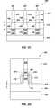
- FIG. 2Ais a simplified plan view of a portion of a memory cell array 200 according to an embodiment of the present disclosure.
- the memory cell array 200may include a plurality of vertical memory cells 201 coupled to a plurality of access lines. Access lines may include a plurality of digit lines 204 (indicated with dashed lines), a plurality of word lines 214 (indicated with dashed lines), and a plurality of body connection lines 218 (indicated with dashed lines).
- the memory cell array 200may be arranged in rows (vertical memory cells 201 coupled to a common digit line 204 ) and columns (vertical memory cells 201 coupled to a common word line 214 ).
- Individual vertical memory cells 201may be located at a cross-point of a digit line 204 and a word line 214 .
- the columns and rowsmay not necessarily physically resemble columns and rows, but are more of an indication of the logical organization for selecting vertical memory cells 201 within the memory cell array 200 .
- the digit lines 204 and word lines 214may extend in directions that are orthogonal to each other, such that the physical configuration of the vertical memory cells 201 may appear as rows and columns.
- the digit lines 204may extend along the substrate 202 ( FIG. 2B ) to a digit line contact pillar 230
- the body connection lines 218may extend along the substrate 202 to a body connection line contact pillar 228 .
- Each of the plurality of body connection lines 218may run parallel with a corresponding digit line 204 .
- FIG. 2Ashows each body connection line 218 as having a narrower width than a width of the corresponding digit line 204 , such as is shown for convenience in distinguishing between the body connection line 218 and the digit line 204 for the plan view shown.
- Embodiments of the present disclosuremay include body connection lines 218 and digit lines 204 that have widths that are at least substantially equal.
- some embodimentsmay include body connection lines 218 and digit lines 204 that have widths that are different.
- the memory cell array 200may also include the plurality of digit line contact pillars 230 and the plurality of body connection line contact pillars 228 .
- the digit line contact pillars 230electrically couple with the corresponding digit lines 204 for applying a voltage thereto.
- the body connection line contact pillars 228electrically couple with the corresponding body connection lines 218 for applying a voltage thereto.
- a dielectric material 212may also be disposed around the vertical memory cells 201 , the body connection line contact pillars 238 , and the digit line contact pillars 230 .
- the dielectric material 212may comprise silicon dioxide, silicon nitride, high-k dielectric material, low-k dielectric material, and combinations thereof.
- the memory cell array 200may further include one or more isolation regions 244 comprising the dielectric material 212 .
- the one or more isolation regions 244may be configured to electrically isolate one or more of the plurality of digit lines 204 and one or more of the plurality of body connection lines 218 from another of the plurality of digit lines 204 and another of the plurality of body connection lines 218 .
- the isolation region 244may electrically isolate the digit line contact pillars 230 from another set of digit line contact pillars 230 that are disposed at a beginning of another set of digit lines 204 in the same corresponding rows of the memory cell array 200 .
- another set of body connection line contact pillars 228may be disposed at a beginning of another set of body connection lines 218 of the memory cell array 200 .
- the plurality of body connection line contact pillars 228 and the plurality of digit line contact pillars 230may be located only at ends of each row of the memory cell array 200 .
- FIG. 2Bis a simplified cross-sectional view of the portion of the memory cell array 200 taken along line 2 B of FIG. 2A .
- the cross-section of FIG. 2Bis taken along the digit line 204 of the memory cell array 200 .
- the word line 214extends in a direction orthogonal to the cross-section of FIG. 2B .
- the memory cell array 200may include the plurality of vertical memory cells 201 disposed on a substrate 202 .
- Each of the plurality of vertical memory cells 201may include a body region 206 , an electrode 208 , and a storage element 210 stacked in a vertical arrangement.
- the storage element 210may be disposed on the electrode 208 , which may be disposed on the body region 206 .
- the body region 206may be coupled to the digit line 204 .
- the digit line 204 , the body region 206 , and the electrode 208may faun a vertical access transistor for the storage element 210 , with the word line 214 acting as a gate.
- the electrode 208may comprise a first source/drain region and the digit line 204 may comprise a second source/drain region forming the vertical access transistor for the storage element 210 .
- the term “source/drain region”is used to indicate that such a region may function as either a source region or a drain region for a vertical access transistor depending on an operational state of the vertical access transistor.
- the first source/drain regionmay be function as a source while the second source/drain region functions as a drain, and vice versa.
- the first source/drain regionmay function as a either a source region or a drain region to the vertical access transistor depending on the operation of the vertical access transistor.
- the second source/drain regionmay function as either a source region or a drain region to the vertical access transistor depending on the operation of the vertical access transistor.
- the digit line 204 , the body region 206 , and the electrode 208may each comprise a doped semiconductor material to form a vertical access transistor for the storage element 210 .
- the digit line 204may comprise n-type semiconductor material
- the body region 206may comprise p-type semiconductor material
- the electrode 208may comprise n-type semiconductor material to form a vertical npn transistor that is activated by the word line 214 acting as the gate.
- the digit line 204may comprise p-type semiconductor material
- the body region 206may comprise n-type semiconductor material
- the electrode 208may comprise p-type semiconductor material to form a vertical pnp transistor that is activated by the word line 214 acting as the gate.
- the second source/drain region and the digit line 204may be a single integrally formed region, while other embodiments may include discrete regions for the second source/drain region and the digit line 204 .
- digit lineis intended to cover each embodiment unless specifically described otherwise.
- word lineis intended to cover embodiments of a single metal electrode acting as a word line and a gate, or a separate word line electrically coupled to a discrete gate formed at each vertical memory cell 201 .
- Each body region 206may be disposed on a body connection line 218 of the plurality of body connection lines 218 .
- the body region 206may be integrally formed with the body connection line 218 such that a single integral structure may be present.
- the body region 206 and the body connection line 218may be formed by separate fabrication operations such that discrete features may be formed.
- the body region 206 being “disposed” on the body connection line 218includes both embodiments of a single integral feature and separate features unless specifically described otherwise.
- Each body connection line 218may extend in parallel with a corresponding digit line 204 along the memory cell array 200 .
- each of the plurality of body connection lines 218may extend at least substantially continuously along the length of the corresponding digit line 204 .
- the individual body connection lines 218may be at least substantially coextensive with its corresponding digit line 204 , recognizing that the corresponding digit lines 204 may extend at least somewhat beyond the body connection line contact pillars 228 to accommodate placement of the body connection line contact pillars 228 and the digit line contact pillars 230 .
- each corresponding digit line 204may extend past the end of each body connection line 218 where a digit line contact pillar 230 may be disposed.
- Extension of the corresponding digit lines 204 past the ends of the body connection lines 218 to the digit line contact pillars 230may enable contact of the digit lines 204 and the digit line contact pillars 230 without interrupting the body connection lines 218 between the vertical memory cells 201 and the body connection line contact pillars 228 .
- there may be a plurality of body connection line contact pillars 228 at intermediate locations along the body connection line 218 for a group of vertical memory cells 201whereas the digit line contact pillars 230 may be located on one or more of the ends of the group of vertical memory cells 201 .
- Each of the plurality of body connection lines 218may have a thickness (T) in a vertical direction.
- the thickness (T) of the plurality of body connection lines 218may affect the series resistance (and, therefore, the conductivity) of the plurality of body connection lines 218 in a direction parallel to the plurality of body connection lines 218 . Additionally, the thickness (T) may affect the mechanical properties of the plurality of body connection lines 218 .
- the thickness of the word lines 214 and the digit lines 204may likewise affect electrical and mechanical properties of the respective word lines 214 and digit lines 204 .
- the body region 206may comprise doped semiconductor material of the same carrier type as the body connection line 218 .
- the doping concentration of the body connection line 218 and the body region 206may differ.
- the doped semiconductor material of the body connection line 218may be more heavily doped than the semiconductor material of the body region 206 .
- the body connection line contact pillars 228may comprise a doped semiconductor material of the same carrier type as the plurality of body connection lines 218 .
- the body connection line 218comprises p-type semiconductor material
- the body region 206 and the body connection line contact pillars 228may also comprise p-type semiconductor material.
- the body connection line 218comprises n-type semiconductor material
- the body region 206 and the body connection line contact pillars 228may also comprise n-type semiconductor material.
- the electrode 208may comprise doped semiconductor material of the same carrier type as the digit line 204 and the digit line contact pillars 230 .
- the electrode 208 , and the digit line contact pillars 230may also comprise n-type semiconductor material.
- the electrode 208 , and the digit line contact pillars 230may also comprise p-type semiconductor material.
- the digit line 204 and/or the digit line contact pillars 230may optionally include a conductive material (not shown), such as, for example, a metal or polysilicon, disposed underneath or on one or more sides of the doped semiconductor material. Such a conductive material may reduce resistivity and increase current flow through the digit lines 204 .
- Each of the plurality of body connection lines 218may comprise semiconductor material doped with carriers opposite to the carriers of the plurality of digit lines 204 .
- each of the plurality of body connection lines 218may comprise p-type semiconductor material, and each of the plurality of digit lines 204 may comprise n-type semiconductor material.
- each of the plurality of body connection lines 218may comprise n-type semiconductor material, and each of the plurality of digit lines 204 may comprise p-type semiconductor material.
- the word lines 214may comprise a conductive material.
- the word lines 214may comprise at least one material from the group consisting of polysilicon, a metal, and a highly-doped monocrystalline semiconductor material.
- Each of the plurality of word lines 214may extend proximate to one or more of the plurality of body regions 206 .
- FIGS. 2A and 2Billustrate each word line 214 as a pair of conductors proximate to opposite sides of the body regions 206 , the present disclosure is not so limited.
- each word line 214may include a single conductor proximate to a single side of the body regions 206 , or any number of conductors on any number of sides of the body regions 206 .
- each word line 214may at least substantially surround the body regions 206 , as will be discussed below in more detail with respect to FIG. 5 .
- the substrate 202may comprise a semiconductor material.
- the semiconductor materialmay include any of silicon, germanium, III-V semiconductor material, and combinations thereof.
- the substratemay comprise a semiconductor-on-insulator substrate, such as, by way of non-limiting example, a silicon-on-insulator (SOI) substrate, or a silicon-on-sapphire (SOS) substrate.
- SOIsilicon-on-insulator
- SOSsilicon-on-sapphire
- the storage element 210may include any device configured to store digital information.
- the storage element 210may include any of a capacitor, a phase change material, a material comprising ionic or thermal resistive switching properties, a magnetoresistive element, a resistive element, a ferroelectric material, a multiferroic material, or other similar materials.
- FIG. 2Cis a simplified cross-sectional view of the memory cell array 200 taken along the line 2 C of FIG. 2A .
- the cross section of FIG. 2Cis taken along the word line 214 of the memory cell array 200 .
- FIG. 2Cillustrates the substrate 202 , the plurality of digit lines 204 , the plurality of body connection lines 218 , the word line 214 , and the vertical memory cells 201 (shown with dashed lines to indicate presence behind the cross-section).
- the body connection lines 218 and digit lines 204extend in a direction orthogonal to the cross-section of FIG. 2C .
- the word line 214may extend proximate to the body regions 206 between the electrodes 208 and the body connection lines 218 .
- the height (H) of the word line 214may be approximately the same as the body region 206 .
- a top of the word line 214may align approximately with a top of the body region 206
- a bottom of the word line 214may align approximately with a bottom of the body region 206 .
- the top of the body region 206may be an interface 209 between the body region 206 and the electrode 208
- the bottom of the body region 206may be an interface 219 between the body region 206 and the body connection line 218 .
- the height (H) of the word line 214may be approximately uniform as the word line 214 extends across the memory cell array 200 .
- FIG. 2Dis a simplified cross-sectional view of a vertical memory cell 201 of the memory cell array taken along the line 2 D of FIG. 2A .
- the cross-section of FIG. 2Dis taken along the digit line 204 of the memory cell array 200 .
- the word line 214extends in a direction orthogonal to the cross section of FIG. 2D .
- the height (H) of the word line 214may be approximately the same as the body region 206 .
- the word line 214was described above as extending approximately from the top of the body region 206 to approximately the bottom of the body region 206 , this description was not intended to be an exact description.
- the bottom of the word line 214may not extend completely to the bottom of the body region 206 so as to maintain at least some separation of the word line 214 and the body connection line 218 with the dielectric material 212 .
- a combination of voltagesmay be applied to the word lines 214 and the digit lines 204 to access a particular vertical memory cell 201 of the memory cell array 200 .
- a first voltagemay be applied to the body connection line 218 through the body connection line contact pillar 228
- a second voltagemay be applied to a word line 214 through a word line contact (not shown)
- a third voltagemay be applied to the digit line 204 through the digit line contact pillar 230 .
- the first voltagemay be selected to bias a subgroup of the plurality of body regions 206 that are disposed on the one or more of the plurality of body connection lines 218 to a desired voltage. As a result, charge build-up within the plurality of body regions may be encouraged or discouraged, according to the desired operation, providing control over leakage currents and threshold voltages.
- each of the body connection lines 218may have the same first voltage applied thereto.
- all body connection lines 218may be coupled together with each body connection line contact pillar 228 being coupled to a common contact.
- the plurality of body connection lines 218may be grouped in a plurality of subgroups, wherein each subgroup has a connection that is configured to receive a voltage independent of a voltage applied to a different subgroup.
- different subgroups of body connection lines 218may independently have different first voltages applied thereto.
- subgroups of body connection lines 218may be formed by coupling together a subgroup of body connection line contact pillars 228 .
- a first subgroup of body connection lines 218may receive a voltage as its first voltage, while a second subgroup of body connection lines 218 may receive a different voltage as its first voltage.
- a subgroup of body connection lines 218may include one or more body connection lines 218 .
- one or more individual body connection line 218may have an independent connection through its respective body connection line contact pillar 228 .
- each connection(whether for individual body connection lines 218 or a subgroup) may have independent connections that may receive different body voltages as desired.
- a first subgroup of body connection lines 218 connected to the body regions 206 of primarily operationally inactive vertical memory cells 201may have a first voltage selected for reducing operational power applied thereto.
- an active sub-array and an inactive sub-array of the memory cell arraymay receive different body voltages, which may result in a reduced power dissipation than if all active and inactive sub-arrays receive the same body voltage.
- a second subgroup of body connection lines 218 connected to the body regions 206 of operationally active vertical memory cells 201may have a first voltage selected for reducing floating body effects of the active vertical memory cells 201 connected thereto.
- an appropriate second voltagemay be applied to the word line 214 to access a particular vertical memory cell 201 .
- the second voltagemay be selected to cause a first conductive channel 216 (shown in dashed lines to indicate intermittent presence) to form through the body region 206 .
- the second voltagemay be a high voltage that is sufficient to attract electrons in the body region 206 , causing the first conductive channel 216 to form through the body region 206 along an outer periphery of the body region 206 .
- the first conductive channel 216may be formed through the body region 206 , and the storage element 210 may be accessed through the digit line 204 . Accessing the storage element 210 with the digit line 204 may enable read or write operations to the storage element 210 by applying the appropriate third voltage to the digit line 204 through the digit line contact pillar 230 ( FIG. 2A ).
- the body connection line 218may receive an appropriate first voltage through the body connection line contact pillar 228 to provide a path for charges to travel into and out of the body regions 206 of the vertical memory cells 201 , which may reduce at least some of the adverse effects of a floating body that exists in a conventional vertical memory cell. For example, if sufficient conductivity is established between the body connection line contact pillars 228 and the body regions 206 , and an appropriate first voltage is applied to the body connection line contact pillars 228 , the floating body effects may be reduced or eliminated. For example, leakage current from the body regions 206 may be reduced, and power dissipation in the memory cell array 200 may be more consistent and controlled.
- each of the plurality of body connection lines 218is between the body regions 206 and the body connection line contact pillars 228 , the more the floating body effects may be controlled or eliminated.
- the conductivity of the plurality of body connection lines 218 between the body regions 206 and the body connection line contact pillars 228is proportional to the thickness (T) of the plurality of body connection lines 218 . Consequently, it may be desirable for the thickness (T) of the plurality of body connection lines 218 to be relatively large. In some embodiments, the thickness (T) may be at least about 25 nanometers thick.
- an increased thickness (T) of the plurality of body connection lines 218may be desirable to increase the conductivity of the body connection line 218
- the conductivity between the digit line 204 and the body region 206is inversely proportional to the thickness (T) of the plurality of body connection lines 218 .
- An increased thickness (T) of the plurality of body connection lines 218consequently, may decrease the conductivity between the digit lines 204 and the body regions 206 .
- a decreased conductivity between the digit lines 204 and the body regions 206may cause an increased voltage drop between the digit lines 204 and the body regions 206 , which may cut into already narrow threshold voltage ranges in low-voltage systems. Additionally, decreased conductivity between the digit lines 204 and the body regions 206 may decrease drive current, resulting in slower operational speed.
- the word lines 214may optionally be configured to extend toward the substrate 202 , proximate to the body connection lines 218 .
- FIG. 3Ais a simplified cross-sectional view of a memory cell array 200 according to another embodiment of the present disclosure.
- the cross-section of FIG. 3Ais similar to FIG. 2C , being taken along the word line 214 of the memory cell array 200 .
- the memory cell array 200 of FIG. 3Ais similar to FIG. 2C as to the general structure of the memory cell array 200 .
- the difference, however, between FIG. 3A and FIG. 2Cis in the structure of the word line 214 .
- the body connection lines 218 and digit lines 204extend in a direction orthogonal to the cross-section of FIG. 3A .
- the word line 214 of FIG. 2Cmay be substantially uniform as the word line 214 extends across the memory cell array 200 .
- the word line 214 of FIG. 3Amay not be substantially uniform as the word line 214 extends across the memory cell array 200 .
- at least a portion 220 of the word line 214may further extend toward the substrate 202 in the region between neighboring body connection lines 218 .
- This portion 220 of the word line 214may be referred to as a “saddle region” 220 , as the word line 214 may “saddle” (e.g., overlap) the body connection lines 218 by at least partially surrounding the sides of the body connection lines 218 .
- the word line 214therefore, has a first portion that has a height (H), while the saddle region 220 has a height (S) that further extends toward the substrate 202 .
- the saddle region 220may extend at least beyond a top surface of the body connection line 218 in the region between the neighboring body connection lines 218 .
- the saddle region 220 of the word line 214may extend below the interface 219 in the region between the neighboring body connection lines 218 .
- the saddle region 220may extend to a bottom of the body connection line 218 .
- the bottom of the body connection line 218may be an interface 205 between the body connection line 218 and the digit line 204 .
- the saddle region 220may extend toward the substrate 202 beyond the bottom of the body connection lines 218 .
- the saddle region 220may extend toward the substrate 202 with a height (S) such that the saddle region 220 does not extend as far as the bottom of the body connection lines 218 .
- the saddle region 220may be formed by over-etching the dielectric material 212 in the word line 214 trench.
- the shape of the saddle region 220may vary.
- FIG. 3Aillustrates the saddle region 220 shaped as a trapezoidal extension of the word line 214 toward the substrate 202 in the region between neighboring body connection lines 218 .
- the saddle region 220may have square, rectangular, or other similar shapes having sides with distinct angles.
- Other shapes of the saddle region 220may include those having curved sides, such as a half-circle, a parabola, a shape having curved sides with a flat bottom, or other suitable shapes including arcuate peripheral boundaries.
- the saddle region 220may be shaped in any configuration that may enable the word line 214 to function as a gate to at least a portion of the body connection line 218 .
- a portion of the body connection line 218 proximate to the word line 214may be inverted, forming a second conductive channel 226 through the body connection line 218 . If the second voltage is removed from the word line 214 , the section of the body connection line 218 proximate to the word line 214 may be accumulated, causing the second conductive channel 226 to cut off.
- the second conductive channel 226may increase the conductivity between the digit lines 204 and the body regions 206 , which may mitigate at least some of the adverse effects of increasing the thickness (T) of the body connection lines 218 . Consequently, a relatively large thickness (T) of the body connection lines 218 may provide a high conductivity between the body regions 206 and the body connection line contact pillars 228 without sacrificing conductivity between the digit lines 204 and the body regions 206 . Furthermore, the thickness (T) of the body connection lines 218 may be sufficiently large to avoid damage to the body connection lines 218 due to becoming pinched during word line separation etch, which may etch away part of the body connection lines 218 .
- FIG. 3Bis a simplified cross-sectional view of a vertical memory cell 201 of a memory cell array 200 according to another embodiment of the present disclosure.
- the cross-section of FIG. 3Bis similar to FIG. 2D , being taken along the digit line 204 of the memory cell array 200 .
- the memory cell array 200 of FIG. 3Bis similar to FIG. 2D as to the general structure of the vertical memory cell 201 of the memory cell array 200 .
- the difference, however, between FIG. 3B and FIG. 2Dis in the structure of the word line 214 .
- the structure of the word line 214 in FIG. 3Bcorresponds to the structure described with respect to FIG. 3A .
- FIG. 3Bis a different view of the vertical memory cell 201 of FIG. 3A .
- Each of the digit line 204 , the body connection line 218 , the body region 206 , the electrode 208 , and the storage element 210is shown in dashed lines to indicate presence behind the cross-section.
- the cross-section FIG. 3Bis taken at some location between neighboring body connection lines 218 of the memory cell array 200 , where the saddle region 220 exists.
- the word line 214extends in the direction orthogonal to the cross-section of FIG. 3B .
- the saddle region 220extends below the interface 219 toward the substrate 202 .
- the saddle region 220may extend to a bottom of the body connection line 218 , beyond the bottom of the body connection line 218 , or to a distance that does not extend as far as the bottom of the body connection lines 218 .
- the saddle region 220is offset from the body connection lines 218 and the digit lines 204 such that the saddle region will be separated from each by the dielectric material 212 .
- the saddle region 220may cause the second conductive channel 226 to form through the body connection line 218 , which may increase the conductivity between the digit lines 204 and the body regions 206 as discussed above with respect to FIG. 3A .
- FIG. 4is a simplified cross-sectional view of a memory cell array 200 according to another embodiment of the present disclosure.
- the cross-section of FIG. 4is similar to FIG. 2B being taken along the digit line 204 of the memory cell array 200 .
- the word line 214extends in a direction orthogonal to the cross-section of FIG. 4 .
- the memory cell array 200 of FIG. 4is similar to FIG. 2B as to the general structure of the memory cell array 200 .
- the difference, however, between FIG. 2B and FIG. 4is in the structure of the body connection lines 218 .
- the body connection lines 218 of FIG. 4may further include a plurality of pocket regions 234 between the vertical memory cells 201 .
- the pocket regions 234may comprise a semiconductor material that is doped at a higher carrier concentration than the rest of the body connection lines 218 .
- the inclusion of the more highly-doped pocket regions 234may cause the conductivity of the body connection lines 218 as a whole to increase by reducing the resistance of the body connection lines 218 .
- the pocket regions 234may be formed in the body connection lines 218 after the vertical memory cells 201 have been formed on the body connection lines 218 .
- a self-aligned implant operationmay be performed after word line separation.
- Impuritiesmay be implanted to increase the doping of the body connection lines 218 in the pocket regions 234 .
- the body connection lines 218comprise p-type silicon
- impuritiessuch as boron or gallium may be implanted in the pocket regions 234 to increase the number of charge carriers in the pocket regions 234 .
- the body connection lines 218comprise n-type silicon
- impuritiessuch as, for example, phosphorus or arsenic may be implanted into the pocket regions 234 to increase the number of charge carriers in the pocket regions 234 .
- the memory cell array 200may be heated following the implantation of impurities in the pocket regions 234 . If such heating occurs, the impurities may disperse more uniformly throughout the body connection lines 218 .
- FIG. 5is a simplified plan view of a memory cell array 200 according to another embodiment of the present disclosure.
- the plan view of FIG. 5is similar to the plan view illustrated in FIG. 2A .
- the structure of the memory cell array 200 of FIG. 5is similar to that of FIG. 2A .
- the difference between FIG. 5 and FIG. 2Ais in the structure of the word lines 214 .
- the word lines 214 of FIG. 5are configured to at least substantially surround the body regions 206 of the vertical memory cells 201 .
- the word lines 214 of FIG. 5may include a pair of conductors proximate to opposite sides of the body regions 206 .
- the word lines 214 of FIG. 5may include a pair of conductors proximate to opposite sides of the body regions 206 . In contrast to the word lines 214 of FIG.
- the word lines 214 of FIG. 5may additionally couple to each other at locations between the vertical memory cells 201 .
- the word lines 214may be positioned to surround the body regions 206 on each side.
- the word lines 214may be configured to partially surround the body regions 206 on only three sides.
- the word lines 214 of FIG. 5similarly to the word lines 214 of FIG. 2A , may be coupled to a word line contact (not shown) at the end of the memory cell array 200 , at intermediate locations along the memory cell array 200 , or combinations thereof.
- FIG. 6is a simplified flowchart 660 illustrating a method of operating a vertical memory cell (e.g., vertical memory cell 201 of any of FIGS. 2A through 2D , 3 A, 3 B, 4 , and 5 ).
- a first voltagemay be applied to the body connection line 218 of a vertical memory cell 201 having a body connection line 218 extending along the memory cell array 200 to a body connection line contact pillar 228 .
- the body connection line 218may run parallel to the digit line 204 .
- the first voltagemay be selected to bias the body regions 206 to a desired level.
- a second voltagemay be applied to the word line 214 .
- the second voltagemay be selected to cause the body regions 206 to invert and form the first conductive channel 216 in each of the body regions 206 proximate the word line 214 .
- the second voltagemay further cause the second conductive channel 226 to be formed in the body connection lines 218 proximate the saddle regions 220 of the word line 214 .
- a decisionmay be made for selecting an operation to perform on the vertical memory cell 201 .
- Operations that may be selected to perform on the vertical memory cell 201may include a read operation and a write operation. If the read operation is selected, a read operation may be performed at operation 670 .
- Performing a read operationmay comprise any operation for detecting an operational state of the storage element 210 , including applying an appropriate combination of voltages to the appropriate word line 214 and digit line 204 for selecting a particular vertical memory cell 201 from which to read.
- performing a read operationmay include detecting a charge stored on the capacitor.
- Performing a write operationmay include any operation for changing the operational state of the storage element 210 , including applying an appropriate combinations of voltages to the appropriate word line 214 and digit line 204 for selecting a particular vertical memory cell 201 to which to write.
- performing a write operationmay comprise supplying a current to the storage element 210 .
- the currentmay be applied to the storage element 210 by applying an appropriate third voltage to the digit line 204 that underlies the vertical memory cell 201 .
- the second voltagemay be removed from the word line 214 . Removing the second voltage from the word line 214 may cause the first conductive channel 216 to dissipate. Removing the second voltage from the word line 214 may also cause the second conductive channel 226 to dissipate, if such was formed by the presence of the saddle region 220 .
- the memory cell arrays described hereinmay be included within an apparatus.
- the memory cell arraymay include a substrate, a body connection line pillar disposed on the substrate, and a plurality of vertical memory cells disposed on the substrate. Each of the plurality of vertical memory cells may include a body region, and a body connection line extending across the substrate and coupling the body region to the body connection line pillar.
- the apparatusmay comprise a memory device including the memory array.
- the apparatusmay further include an electrical system including the memory device.
- the apparatusmay further include a control circuit and an input device and an output device operably coupled to the control circuit.
- FIG. 7is a simplified block diagram of an electrical system 750 including a vertical memory cell.
- the electrical system 750may include a memory cell array 700 , a control circuit 754 , an input device 756 , and an output device 758 that are operably coupled to communicate with each other through the control circuit 754 .
- the memory cell array 700may include a plurality of vertical memory cells 201 , one or more body connection lines 218 , one or more digit lines 204 , and one or more word lines 214 , as described with reference to FIGS. 2A through 2D , 3 A, 3 B, 4 , and 5 .
- the memory cell array 700may include any combination of features of the memory cell arrays 200 described herein, and/or their equivalents.
- the control circuit 754may be configured to control the memory cell array 700 .
- the control circuit 754may include one or more devices from the group consisting of a processor, a hard disk drive, and an optical disc drive (not shown).
- the control circuit 754may be operably coupled to the digit lines 204 , the body connection lines 218 , and the word lines 214 ( FIGS. 2A through 2D , 3 A, 3 B, 4 , and 5 ) of the memory cell array 700 .
- the control circuit 754may also be configured to apply one or more of a plurality of voltages to the digit lines 204 , the body connection lines 218 , and the word lines 214 of the memory cell array 700 .
- the control circuit 754may be further configured to perform read and write operations on the memory cell array 700 .
- the control circuit 754may also be operably coupled to the input device 756 , and the output device 758 .
- the input device 756may include any of a keyboard, a button array, a mouse device, a touch screen input, other similar devices, and combinations thereof.
- the control circuit 754may be configured to receive and execute commands, and receive information, from the input device 756 .
- the output device 758may include, by way of non-limiting example, any of a liquid crystal display (LCD) device, a light-emitting diode (LED) array, a cathode ray tube (CRT) display, a sound generating device, an electrical signal output port, other similar devices, and combinations thereof.
- the control circuit 754may be configured to cause the output device 758 to communicate information to a user (not shown) or another device (not shown).
Landscapes
- Engineering & Computer Science (AREA)
- Manufacturing & Machinery (AREA)
- Microelectronics & Electronic Packaging (AREA)
- Computer Hardware Design (AREA)
- Semiconductor Memories (AREA)
- General Engineering & Computer Science (AREA)
Abstract
Description
- The present disclosure relates to vertical memory cells and memory arrays, and more particularly to vertical access devices having a body connection line.
- The use of an access device with a storage element in memory cells is well known in the art. Examples of memory devices that utilize access devices include dynamic random-access memory (DRAM), resistive random-access memory (RRAM), magnetoresistive random-access memory (MRAM), and phase-change random-access memory (PRAM).
- An ever-increasing demand for higher-density memory cell arrays has lead to the development of vertical memory cell devices. Vertical memory cell devices may enable higher-density cell arrays by offsetting an access device vertically from a storage element, thereby requiring less horizontal area than if the access device were offset horizontally from the storage element.
FIG. 1A is a simplified plan view of a portion of a conventionalmemory cell array 100. The conventionalmemory cell array 100 includes a plurality ofvertical memory cells 101, a plurality of digit lines104 (in dashed lines to show they are buried), and a plurality of word lines114 (in dashed lines to show they are buried). Thevertical memory cells 101 are arranged in rows (coupled to a common digit line104) and columns (coupled to a common word line114). Individualvertical memory cells 101 are located at a cross-point of adigit line 104 and aword line 114.FIG. 1B is a simplified cross-sectional view of avertical memory cell 101 taken alongline 1B ofFIG. 1A . Thevertical memory cell 101 may be formed on asubstrate 102. Thevertical memory cell 101 includes adigit line 104, abody region 106 disposed on thedigit line 104, anelectrode 108 disposed on thebody region 106, aword line 114 proximate to thebody region 106, and a storage element110 (e.g., a capacitor) disposed on theelectrode 108. Thevertical memory cell 101 also includes adielectric material 112 on thesubstrate 102, and surrounding thevertical memory cell 101. Thedielectric material 112 insulates thebody region 106 from theword line 114.- A portion of the
dielectric material 112 located between thebody region 106 and theword line 114 is configured as a gate dielectric, and may comprise a dielectric with properties that are different from those of the remainder of thedielectric material 112. - The
vertical memory cell 101 is configured to establish electrical connection and isolation between thedigit line 104 and thestorage element 110. In other words, thedigit line 104, thebody region 106, and theelectrode 108 form an access transistor, with theword line 114 acting as its gate. In operation, a first voltage is applied to theword line 114, which may attract charge carriers to a segment of thebody region 106 that is proximate to theword line 114. As a result, a conductive channel116 (in dashed lines to show intermittent presence) may be formed through thebody region 106 between thedigit line 104 and theelectrode 108. Theconductive channel 116 enables thedigit line 104 to access thestorage element 110 for read or write operations. - If the first voltage is removed from the
word line 114, theconductive channel 116 may be cut off, electrically isolating thestorage element 110 from thedigit line 104. As a result, by selectively applying the first voltage to theword line 114, electrical connection and isolation between thedigit line 104 and thestorage element 110 may be established. In addition, different combinations of voltages may be applied to theword line 114 and thedigit line 104 to select a particularvertical memory cell 101 from the conventionalmemory cell array 100 for a read or write operation. - Although the
vertical memory cell 101 may successfully establish electrical connection and isolation between thedigit line 104 and thestorage element 110, thebody region 106 is a floating body. Consequently, thevertical memory cell 101 suffers from floating body effects, which may result in degraded charge retention time in the case of DRAM devices, and power distribution problems in the conventionalmemory cell array 100. FIG. 1A is a simplified plan view of a portion of a conventional memory cell array;FIG. 1B is a simplified cross-sectional view of a conventional vertical memory cell taken alongline 1B ofFIG. 1A ;FIG. 2A is a simplified plan view of a portion of a memory cell array;FIG. 2B is a simplified cross-sectional view of the memory cell array ofFIG. 2A taken alongline 2B ofFIG. 2A ;FIG. 2C is a simplified cross-sectional view of the memory cell array ofFIG. 2A taken alongline 2C ofFIG. 2A ;FIG. 2D is a simplified cross-sectional view of a vertical memory cell of the memory cell array ofFIG. 2A taken alongline 2D ofFIG. 2A ;FIG. 3A is a simplified cross-sectional view of a memory cell array;FIG. 3B is a simplified cross-sectional view of a memory cell array;FIG. 4 is a simplified cross-sectional view of a memory cell array;FIG. 5 is a simplified plan view of a memory cell array;FIG. 6 is a simplified flowchart illustrating a method of operating a vertical memory cell; andFIG. 7 is a simplified block diagram of an electrical system including a vertical memory cell.- In the following detailed description, reference is made to the accompanying drawings that form a part hereof, and in which is shown by way of illustration specific embodiments in which the present disclosure may be practiced. These embodiments are described in sufficient detail to enable those of ordinary skill in the art to make, use, or otherwise practice the present disclosure. It should be understood, however, that the detailed description and the specific examples, while indicating examples of embodiments of the present disclosure, are given by way of illustration only and not by way of limitation. From this disclosure, various substitutions, modifications, additions, rearrangements, or combinations thereof within the scope of the present disclosure may be made and will become apparent to those of ordinary skill in the art.
- In accordance with common practice, the various features illustrated in the drawings may not be drawn to scale. The illustrations presented herein are not meant to be actual views of any particular method, device, or system, but are merely idealized representations that are employed to describe various embodiments of the present disclosure. Accordingly, the dimensions of how various features are depicted may be arbitrarily expanded or reduced for clarity. In addition, some of the drawings may be simplified for clarity. Thus, the drawings may not depict all of the components of a given apparatus (e.g., device, system, etc.) or all operations of a particular method.
- Information and signals described herein may be represented using any of a variety of different technologies and techniques. For example, data, instructions, commands, information, signals, bits, symbols, and chips that may be referenced throughout the description may be represented by voltages, currents, electromagnetic waves, magnetic fields or particles, optical fields or particles, or any combination thereof. Some drawings may illustrate signals as a single signal for clarity of presentation and description. It should be understood by a person of ordinary skill in the art that the signal may represent a bus of signals, wherein the bus may have a variety of bit widths and the present disclosure may be implemented on any number of data signals including a single data signal.
- In addition, the various illustrative logical blocks, modules, circuits, and algorithm acts described in connection with embodiments disclosed herein may be implemented as electronic hardware, computer software, or combinations of both. To clearly illustrate this interchangeability of hardware and software, various illustrative components, blocks, modules, circuits, and acts are described generally in terms of their functionality. Whether such functionality is implemented as hardware or software depends upon the particular application and design constraints imposed on the overall system. Skilled artisans may implement the described functionality in varying ways for each particular application, but such implementation decisions should not be interpreted as causing a departure from the scope of the embodiments of the disclosure described herein.
- In addition, it is noted that some embodiments may be described in terms of a process that is depicted as a flowchart, a flow diagram, a structure diagram, or a block diagram. Although a flowchart may describe operational acts as a sequential process, many of these operational acts can be performed in another sequence, in parallel, or substantially concurrently. In addition, the order of the operational acts may be re-arranged. A process may correspond to a method, a function, a procedure, a subroutine, a subprogram, etc. Furthermore, the methods disclosed herein may be implemented in hardware, software, or both. If implemented in software, the functions may be stored or transmitted as one or more instructions or code on a computer-readable medium. Computer-readable media includes both computer storage media and communication media including any medium that facilitates transfer of a computer program from one place to another.
- It should be understood that any reference to an element herein using a designation such as “first,” “second,” and so forth does not limit the quantity or order of those elements, unless such limitation is explicitly stated. Rather, these designations may be used herein as a convenient method of distinguishing between two or more elements or instances of an element. Thus, a reference to a first element and a second element does not mean that only two elements may be employed there or that the first element must precede the second element in some manner. Also, unless stated otherwise a set of elements may comprise one or more elements.
- Elements described herein may include multiple instances of the same element. These elements may be generically indicated by reference numerals (e.g.,110). For ease of following the description, for the most part, reference numerals begin with the number of the drawing on which the elements are introduced or most fully discussed. Thus, for example, reference numerals introduced on a
FIG. 1 will be mostly in the numerical format 1xx and elements introduced on aFIG. 4 will be mostly in the numerical format 4xx. In addition, like reference numerals may be used to denote like features throughout the specification and figures. - Embodiments of the present disclosure include systems, methods and devices for providing a body connection to a vertical access device. It should be noted that while the utility and application of the various embodiments of the present disclosure are described with reference to memory arrays, the present disclosure also finds application to any other apparatus (e.g., integrated circuit, memory devices, systems, etc.) where a vertical access device may be desirable.
- In particular, embodiments of the present disclosure include a vertical access device that comprises a digit line extending along a substrate to a digit line contact pillar, a body connection line extending along the substrate to a body connection line contact pillar, a body region disposed on the body connection line, an electrode disposed on the body region, and a word line forming a gate to the body region, the word line separated from the body region by a dielectric. Such a vertical access device may be a vertical memory cell of a memory cell array.
- In additional embodiments, an apparatus may comprise a plurality of vertically-configured access transistors arranged in a plurality of rows and columns, a plurality of word lines and a plurality of digit lines. Each word line of the plurality of word lines may form a gate for a corresponding column of vertically-configured access transistors, and each digit line of the plurality of digit lines may couple to a corresponding row of vertically-configured access transistors. The apparatus may further comprise a plurality of body connection lines, wherein each body connection line of the plurality of body connection lines couples to a plurality of body regions of the plurality of vertically-configured access transistors.
FIG. 2A is a simplified plan view of a portion of amemory cell array 200 according to an embodiment of the present disclosure. Thememory cell array 200 may include a plurality ofvertical memory cells 201 coupled to a plurality of access lines. Access lines may include a plurality of digit lines204 (indicated with dashed lines), a plurality of word lines214 (indicated with dashed lines), and a plurality of body connection lines218 (indicated with dashed lines). Thememory cell array 200 may be arranged in rows (vertical memory cells 201 coupled to a common digit line204) and columns (vertical memory cells 201 coupled to a common word line214). Individualvertical memory cells 201 may be located at a cross-point of adigit line 204 and aword line 214. The columns and rows may not necessarily physically resemble columns and rows, but are more of an indication of the logical organization for selectingvertical memory cells 201 within thememory cell array 200. The digit lines204 andword lines 214, however, may extend in directions that are orthogonal to each other, such that the physical configuration of thevertical memory cells 201 may appear as rows and columns.- The digit lines204 may extend along the substrate202 (
FIG. 2B ) to a digitline contact pillar 230, the body connection lines218 may extend along thesubstrate 202 to a body connectionline contact pillar 228. Each of the plurality of body connection lines218 may run parallel with acorresponding digit line 204. AlthoughFIG. 2A shows eachbody connection line 218 as having a narrower width than a width of thecorresponding digit line 204, such as is shown for convenience in distinguishing between thebody connection line 218 and thedigit line 204 for the plan view shown. Embodiments of the present disclosure, however, may includebody connection lines 218 anddigit lines 204 that have widths that are at least substantially equal. Of course, some embodiments may includebody connection lines 218 anddigit lines 204 that have widths that are different. - The
memory cell array 200 may also include the plurality of digitline contact pillars 230 and the plurality of body connectionline contact pillars 228. The digitline contact pillars 230 electrically couple with thecorresponding digit lines 204 for applying a voltage thereto. The body connectionline contact pillars 228 electrically couple with the correspondingbody connection lines 218 for applying a voltage thereto. - A
dielectric material 212 may also be disposed around thevertical memory cells 201, the body connection line contact pillars238, and the digitline contact pillars 230. By way of non-limiting example, thedielectric material 212 may comprise silicon dioxide, silicon nitride, high-k dielectric material, low-k dielectric material, and combinations thereof. - The
memory cell array 200 may further include one ormore isolation regions 244 comprising thedielectric material 212. The one ormore isolation regions 244 may be configured to electrically isolate one or more of the plurality ofdigit lines 204 and one or more of the plurality ofbody connection lines 218 from another of the plurality ofdigit lines 204 and another of the plurality of body connection lines218. For example, theisolation region 244 may electrically isolate the digitline contact pillars 230 from another set of digitline contact pillars 230 that are disposed at a beginning of another set ofdigit lines 204 in the same corresponding rows of thememory cell array 200. Following the other set of digitline contact pillars 230, another set of body connectionline contact pillars 228 may be disposed at a beginning of another set of body connection lines218 of thememory cell array 200. In some embodiments, the plurality of body connectionline contact pillars 228 and the plurality of digitline contact pillars 230 may be located only at ends of each row of thememory cell array 200. FIG. 2B is a simplified cross-sectional view of the portion of thememory cell array 200 taken alongline 2B ofFIG. 2A . In particular, the cross-section ofFIG. 2B is taken along thedigit line 204 of thememory cell array 200. For clarity, it is noted that theword line 214 extends in a direction orthogonal to the cross-section ofFIG. 2B .- The
memory cell array 200 may include the plurality ofvertical memory cells 201 disposed on asubstrate 202. Each of the plurality ofvertical memory cells 201 may include abody region 206, anelectrode 208, and astorage element 210 stacked in a vertical arrangement. In other words, thestorage element 210 may be disposed on theelectrode 208, which may be disposed on thebody region 206. Thebody region 206 may be coupled to thedigit line 204. As a result, thedigit line 204, thebody region 206, and theelectrode 208 may faun a vertical access transistor for thestorage element 210, with theword line 214 acting as a gate. Thus, theelectrode 208 may comprise a first source/drain region and thedigit line 204 may comprise a second source/drain region forming the vertical access transistor for thestorage element 210. The term “source/drain region” is used to indicate that such a region may function as either a source region or a drain region for a vertical access transistor depending on an operational state of the vertical access transistor. Thus, the first source/drain region may be function as a source while the second source/drain region functions as a drain, and vice versa. Thus, the first source/drain region may function as a either a source region or a drain region to the vertical access transistor depending on the operation of the vertical access transistor. Likewise, the second source/drain region may function as either a source region or a drain region to the vertical access transistor depending on the operation of the vertical access transistor. - The
digit line 204, thebody region 206, and theelectrode 208 may each comprise a doped semiconductor material to form a vertical access transistor for thestorage element 210. For example, thedigit line 204 may comprise n-type semiconductor material, thebody region 206 may comprise p-type semiconductor material, and theelectrode 208 may comprise n-type semiconductor material to form a vertical npn transistor that is activated by theword line 214 acting as the gate. Similarly, in some embodiments, thedigit line 204 may comprise p-type semiconductor material, thebody region 206 may comprise n-type semiconductor material, and theelectrode 208 may comprise p-type semiconductor material to form a vertical pnp transistor that is activated by theword line 214 acting as the gate. In some embodiments, the second source/drain region and thedigit line 204 may be a single integrally formed region, while other embodiments may include discrete regions for the second source/drain region and thedigit line 204. For simplicity, the term “digit line” is intended to cover each embodiment unless specifically described otherwise. Similarly, “word line” is intended to cover embodiments of a single metal electrode acting as a word line and a gate, or a separate word line electrically coupled to a discrete gate formed at eachvertical memory cell 201. - Each
body region 206 may be disposed on abody connection line 218 of the plurality of body connection lines218. Thebody region 206 may be integrally formed with thebody connection line 218 such that a single integral structure may be present. In some embodiments, thebody region 206 and thebody connection line 218 may be formed by separate fabrication operations such that discrete features may be formed. As a result, thebody region 206 being “disposed” on thebody connection line 218 includes both embodiments of a single integral feature and separate features unless specifically described otherwise. - Each
body connection line 218 may extend in parallel with acorresponding digit line 204 along thememory cell array 200. In other words, each of the plurality of body connection lines218 may extend at least substantially continuously along the length of thecorresponding digit line 204. In some embodiments, the individual body connection lines218 may be at least substantially coextensive with itscorresponding digit line 204, recognizing that thecorresponding digit lines 204 may extend at least somewhat beyond the body connectionline contact pillars 228 to accommodate placement of the body connectionline contact pillars 228 and the digitline contact pillars 230. In other words, eachcorresponding digit line 204 may extend past the end of eachbody connection line 218 where a digitline contact pillar 230 may be disposed. Extension of thecorresponding digit lines 204 past the ends of thebody connection lines 218 to the digitline contact pillars 230 may enable contact of thedigit lines 204 and the digitline contact pillars 230 without interrupting thebody connection lines 218 between thevertical memory cells 201 and the body connectionline contact pillars 228. In some embodiments, there may be a different number of body connectionline contact pillars 228 and digitline contact pillars 230. For example, there may be a plurality of body connectionline contact pillars 228 at intermediate locations along thebody connection line 218 for a group ofvertical memory cells 201, whereas the digitline contact pillars 230 may be located on one or more of the ends of the group ofvertical memory cells 201. - Each of the plurality of body connection lines218 may have a thickness (T) in a vertical direction. The thickness (T) of the plurality of body connection lines218 may affect the series resistance (and, therefore, the conductivity) of the plurality of
body connection lines 218 in a direction parallel to the plurality of body connection lines218. Additionally, the thickness (T) may affect the mechanical properties of the plurality of body connection lines218. The thickness of the word lines214 and thedigit lines 204 may likewise affect electrical and mechanical properties of therespective word lines 214 anddigit lines 204. - The
body region 206 may comprise doped semiconductor material of the same carrier type as thebody connection line 218. In some embodiments, the doping concentration of thebody connection line 218 and thebody region 206 may differ. By way of non-limiting example, the doped semiconductor material of thebody connection line 218 may be more heavily doped than the semiconductor material of thebody region 206. In addition, the body connectionline contact pillars 228 may comprise a doped semiconductor material of the same carrier type as the plurality of body connection lines218. Also by way of non-limiting example, if thebody connection line 218 comprises p-type semiconductor material, thebody region 206 and the body connectionline contact pillars 228 may also comprise p-type semiconductor material. Similarly, if thebody connection line 218 comprises n-type semiconductor material, thebody region 206 and the body connectionline contact pillars 228 may also comprise n-type semiconductor material. - The
electrode 208 may comprise doped semiconductor material of the same carrier type as thedigit line 204 and the digitline contact pillars 230. By way of non-limiting example, if thedigit line 204 comprises n-type semiconductor material, theelectrode 208, and the digitline contact pillars 230 may also comprise n-type semiconductor material. Similarly, if thedigit line 204 comprises p-type semiconductor material, theelectrode 208, and the digitline contact pillars 230 may also comprise p-type semiconductor material. In some embodiments, thedigit line 204 and/or the digitline contact pillars 230 may optionally include a conductive material (not shown), such as, for example, a metal or polysilicon, disposed underneath or on one or more sides of the doped semiconductor material. Such a conductive material may reduce resistivity and increase current flow through the digit lines204. - Each of the plurality of body connection lines218 may comprise semiconductor material doped with carriers opposite to the carriers of the plurality of digit lines204. By way of non-limiting example, each of the plurality of body connection lines218 may comprise p-type semiconductor material, and each of the plurality of
digit lines 204 may comprise n-type semiconductor material. Similarly, each of the plurality of body connection lines218 may comprise n-type semiconductor material, and each of the plurality ofdigit lines 204 may comprise p-type semiconductor material. - The word lines214 may comprise a conductive material. By way of non-limiting example, the word lines214 may comprise at least one material from the group consisting of polysilicon, a metal, and a highly-doped monocrystalline semiconductor material. Each of the plurality of
word lines 214 may extend proximate to one or more of the plurality ofbody regions 206. AlthoughFIGS. 2A and 2B illustrate eachword line 214 as a pair of conductors proximate to opposite sides of thebody regions 206, the present disclosure is not so limited. In some embodiments, eachword line 214 may include a single conductor proximate to a single side of thebody regions 206, or any number of conductors on any number of sides of thebody regions 206. For embodiments that include a pair of conductors for asingle word line 214, the pair of conductors may be coupled together by a word line contact (not shown) at the end of thememory cell array 200, at intermediate locations of thememory cell array 200, or combinations thereof. Additionally, eachword line 214 may at least substantially surround thebody regions 206, as will be discussed below in more detail with respect toFIG. 5 . - The
substrate 202 may comprise a semiconductor material. By way of non-limiting example, the semiconductor material may include any of silicon, germanium, III-V semiconductor material, and combinations thereof. In some embodiments, the substrate may comprise a semiconductor-on-insulator substrate, such as, by way of non-limiting example, a silicon-on-insulator (SOI) substrate, or a silicon-on-sapphire (SOS) substrate. - The
storage element 210 may include any device configured to store digital information. By way of non-limiting example, thestorage element 210 may include any of a capacitor, a phase change material, a material comprising ionic or thermal resistive switching properties, a magnetoresistive element, a resistive element, a ferroelectric material, a multiferroic material, or other similar materials. FIG. 2C is a simplified cross-sectional view of thememory cell array 200 taken along theline 2C ofFIG. 2A . In particular, the cross section ofFIG. 2C is taken along theword line 214 of thememory cell array 200.FIG. 2C illustrates thesubstrate 202, the plurality ofdigit lines 204, the plurality of body connection lines218, theword line 214, and the vertical memory cells201 (shown with dashed lines to indicate presence behind the cross-section). For clarity, it is noted that thebody connection lines 218 anddigit lines 204 extend in a direction orthogonal to the cross-section ofFIG. 2C .- The
word line 214 may extend proximate to thebody regions 206 between theelectrodes 208 and the body connection lines218. The height (H) of theword line 214 may be approximately the same as thebody region 206. In some embodiments, a top of theword line 214 may align approximately with a top of thebody region 206, and a bottom of theword line 214 may align approximately with a bottom of thebody region 206. The top of thebody region 206 may be aninterface 209 between thebody region 206 and theelectrode 208, while the bottom of thebody region 206 may be aninterface 219 between thebody region 206 and thebody connection line 218. In some embodiments (as shown inFIG. 2C ), the height (H) of theword line 214 may be approximately uniform as theword line 214 extends across thememory cell array 200. FIG. 2D is a simplified cross-sectional view of avertical memory cell 201 of the memory cell array taken along theline 2D ofFIG. 2A . In particular, the cross-section ofFIG. 2D is taken along thedigit line 204 of thememory cell array 200. For clarity, it is noted that theword line 214 extends in a direction orthogonal to the cross section ofFIG. 2D .- As discussed above, the height (H) of the
word line 214 may be approximately the same as thebody region 206. Although theword line 214 was described above as extending approximately from the top of thebody region 206 to approximately the bottom of thebody region 206, this description was not intended to be an exact description. For example, as shown inFIG. 2D , the bottom of theword line 214 may not extend completely to the bottom of thebody region 206 so as to maintain at least some separation of theword line 214 and thebody connection line 218 with thedielectric material 212. - In operation, a combination of voltages may be applied to the word lines214 and the
digit lines 204 to access a particularvertical memory cell 201 of thememory cell array 200. A first voltage may be applied to thebody connection line 218 through the body connectionline contact pillar 228, a second voltage may be applied to aword line 214 through a word line contact (not shown), and a third voltage may be applied to thedigit line 204 through the digitline contact pillar 230. The first voltage may be selected to bias a subgroup of the plurality ofbody regions 206 that are disposed on the one or more of the plurality ofbody connection lines 218 to a desired voltage. As a result, charge build-up within the plurality of body regions may be encouraged or discouraged, according to the desired operation, providing control over leakage currents and threshold voltages. - In some embodiments, each of the body connection lines218 may have the same first voltage applied thereto. For example, in some embodiments all body connection lines218 may be coupled together with each body connection
line contact pillar 228 being coupled to a common contact. In some embodiments, the plurality of body connection lines218 may be grouped in a plurality of subgroups, wherein each subgroup has a connection that is configured to receive a voltage independent of a voltage applied to a different subgroup. In other words, different subgroups of body connection lines218 may independently have different first voltages applied thereto. For example, subgroups of body connection lines218 may be formed by coupling together a subgroup of body connectionline contact pillars 228. Thus, a first subgroup of body connection lines218 may receive a voltage as its first voltage, while a second subgroup of body connection lines218 may receive a different voltage as its first voltage. Of course, any number of subgroups are contemplated, as is the number ofbody connection lines 218 and body connectionline contact pillars 228 that may be part of the same subgroup. As used herein, a subgroup of body connection lines218 may include one or more body connection lines218. For example, in some embodiments, one or more individualbody connection line 218 may have an independent connection through its respective body connectionline contact pillar 228. Thus, each connection (whether for individual body connection lines218 or a subgroup) may have independent connections that may receive different body voltages as desired. By way of non-limiting example, a first subgroup ofbody connection lines 218 connected to thebody regions 206 of primarily operationally inactivevertical memory cells 201 may have a first voltage selected for reducing operational power applied thereto. As a result, an active sub-array and an inactive sub-array of the memory cell array may receive different body voltages, which may result in a reduced power dissipation than if all active and inactive sub-arrays receive the same body voltage. Also by way of non-limiting example, a second subgroup ofbody connection lines 218 connected to thebody regions 206 of operationally activevertical memory cells 201 may have a first voltage selected for reducing floating body effects of the activevertical memory cells 201 connected thereto. - In operation, an appropriate second voltage may be applied to the
word line 214 to access a particularvertical memory cell 201. The second voltage may be selected to cause a first conductive channel216 (shown in dashed lines to indicate intermittent presence) to form through thebody region 206. By way of non-limiting example, if thedigit line 204 and theelectrode 208 comprise n-type semiconductor material, and thebody region 206 and thebody connection line 218 comprise p-type semiconductor material, the second voltage may be a high voltage that is sufficient to attract electrons in thebody region 206, causing the firstconductive channel 216 to form through thebody region 206 along an outer periphery of thebody region 206. The firstconductive channel 216 may be formed through thebody region 206, and thestorage element 210 may be accessed through thedigit line 204. Accessing thestorage element 210 with thedigit line 204 may enable read or write operations to thestorage element 210 by applying the appropriate third voltage to thedigit line 204 through the digit line contact pillar230 (FIG. 2A ). - As discussed above, the
body connection line 218 may receive an appropriate first voltage through the body connectionline contact pillar 228 to provide a path for charges to travel into and out of thebody regions 206 of thevertical memory cells 201, which may reduce at least some of the adverse effects of a floating body that exists in a conventional vertical memory cell. For example, if sufficient conductivity is established between the body connectionline contact pillars 228 and thebody regions 206, and an appropriate first voltage is applied to the body connectionline contact pillars 228, the floating body effects may be reduced or eliminated. For example, leakage current from thebody regions 206 may be reduced, and power dissipation in thememory cell array 200 may be more consistent and controlled. - The more conductive each of the plurality of body connection lines218 is between the
body regions 206 and the body connectionline contact pillars 228, the more the floating body effects may be controlled or eliminated. The conductivity of the plurality ofbody connection lines 218 between thebody regions 206 and the body connectionline contact pillars 228 is proportional to the thickness (T) of the plurality of body connection lines218. Consequently, it may be desirable for the thickness (T) of the plurality ofbody connection lines 218 to be relatively large. In some embodiments, the thickness (T) may be at least about 25 nanometers thick. - Although an increased thickness (T) of the plurality of body connection lines218 may be desirable to increase the conductivity of the
body connection line 218, the conductivity between thedigit line 204 and thebody region 206 is inversely proportional to the thickness (T) of the plurality of body connection lines218. An increased thickness (T) of the plurality of body connection lines218, consequently, may decrease the conductivity between thedigit lines 204 and thebody regions 206. - A decreased conductivity between the
digit lines 204 and thebody regions 206 may cause an increased voltage drop between thedigit lines 204 and thebody regions 206, which may cut into already narrow threshold voltage ranges in low-voltage systems. Additionally, decreased conductivity between thedigit lines 204 and thebody regions 206 may decrease drive current, resulting in slower operational speed. To mitigate the decreased conductivity between thedigit lines 204 and thebody regions 206, the word lines214 may optionally be configured to extend toward thesubstrate 202, proximate to the body connection lines218. FIG. 3A is a simplified cross-sectional view of amemory cell array 200 according to another embodiment of the present disclosure. The cross-section ofFIG. 3A is similar toFIG. 2C , being taken along theword line 214 of thememory cell array 200. In addition, thememory cell array 200 ofFIG. 3A is similar toFIG. 2C as to the general structure of thememory cell array 200. The difference, however, betweenFIG. 3A andFIG. 2C is in the structure of theword line 214. For clarity, it is noted that thebody connection lines 218 anddigit lines 204 extend in a direction orthogonal to the cross-section ofFIG. 3A .- As discussed above, the
word line 214 ofFIG. 2C may be substantially uniform as theword line 214 extends across thememory cell array 200. Theword line 214 ofFIG. 3A , however, may not be substantially uniform as theword line 214 extends across thememory cell array 200. For example, at least aportion 220 of theword line 214 may further extend toward thesubstrate 202 in the region between neighboring body connection lines218. Thisportion 220 of theword line 214 may be referred to as a “saddle region”220, as theword line 214 may “saddle” (e.g., overlap) thebody connection lines 218 by at least partially surrounding the sides of the body connection lines218. Theword line 214, therefore, has a first portion that has a height (H), while thesaddle region 220 has a height (S) that further extends toward thesubstrate 202. - The
saddle region 220 may extend at least beyond a top surface of thebody connection line 218 in the region between the neighboring body connection lines218. In other words, thesaddle region 220 of theword line 214 may extend below theinterface 219 in the region between the neighboring body connection lines218. By way of non-limiting example, thesaddle region 220 may extend to a bottom of thebody connection line 218. The bottom of thebody connection line 218 may be aninterface 205 between thebody connection line 218 and thedigit line 204. The present disclosure, however, is not so limited. In some embodiments, thesaddle region 220 may extend toward thesubstrate 202 beyond the bottom of the body connection lines218. In other embodiments, thesaddle region 220 may extend toward thesubstrate 202 with a height (S) such that thesaddle region 220 does not extend as far as the bottom of the body connection lines218. - The
saddle region 220 may be formed by over-etching thedielectric material 212 in theword line 214 trench. The shape of thesaddle region 220 may vary. By way of non-limiting example,FIG. 3A illustrates thesaddle region 220 shaped as a trapezoidal extension of theword line 214 toward thesubstrate 202 in the region between neighboring body connection lines218. Other shapes are also contemplated. For example, thesaddle region 220 may have square, rectangular, or other similar shapes having sides with distinct angles. Other shapes of thesaddle region 220 may include those having curved sides, such as a half-circle, a parabola, a shape having curved sides with a flat bottom, or other suitable shapes including arcuate peripheral boundaries. In general, thesaddle region 220 may be shaped in any configuration that may enable theword line 214 to function as a gate to at least a portion of thebody connection line 218. - In operation, if the second voltage is applied to the
word line 214, a portion of thebody connection line 218 proximate to theword line 214 may be inverted, forming a secondconductive channel 226 through thebody connection line 218. If the second voltage is removed from theword line 214, the section of thebody connection line 218 proximate to theword line 214 may be accumulated, causing the secondconductive channel 226 to cut off. - The second
conductive channel 226 may increase the conductivity between thedigit lines 204 and thebody regions 206, which may mitigate at least some of the adverse effects of increasing the thickness (T) of the body connection lines218. Consequently, a relatively large thickness (T) of the body connection lines218 may provide a high conductivity between thebody regions 206 and the body connectionline contact pillars 228 without sacrificing conductivity between thedigit lines 204 and thebody regions 206. Furthermore, the thickness (T) of the body connection lines218 may be sufficiently large to avoid damage to thebody connection lines 218 due to becoming pinched during word line separation etch, which may etch away part of the body connection lines218. FIG. 3B is a simplified cross-sectional view of avertical memory cell 201 of amemory cell array 200 according to another embodiment of the present disclosure. The cross-section ofFIG. 3B is similar toFIG. 2D , being taken along thedigit line 204 of thememory cell array 200. In addition, thememory cell array 200 ofFIG. 3B is similar toFIG. 2D as to the general structure of thevertical memory cell 201 of thememory cell array 200. The difference, however, betweenFIG. 3B andFIG. 2D is in the structure of theword line 214. In particular, the structure of theword line 214 inFIG. 3B corresponds to the structure described with respect toFIG. 3A . In other words, the cross-sectional view inFIG. 3B is a different view of thevertical memory cell 201 ofFIG. 3A . Each of thedigit line 204, thebody connection line 218, thebody region 206, theelectrode 208, and thestorage element 210 is shown in dashed lines to indicate presence behind the cross-section. Thus, the cross-sectionFIG. 3B is taken at some location between neighboring body connection lines218 of thememory cell array 200, where thesaddle region 220 exists. For clarity, it is noted that theword line 214 extends in the direction orthogonal to the cross-section ofFIG. 3B .- As shown in
FIG. 3B , thesaddle region 220 extends below theinterface 219 toward thesubstrate 202. As discussed above with respect toFIG. 3A , thesaddle region 220 may extend to a bottom of thebody connection line 218, beyond the bottom of thebody connection line 218, or to a distance that does not extend as far as the bottom of the body connection lines218. As is apparent fromFIG. 3A , thesaddle region 220 is offset from thebody connection lines 218 and thedigit lines 204 such that the saddle region will be separated from each by thedielectric material 212. - In operation, the
saddle region 220 may cause the secondconductive channel 226 to form through thebody connection line 218, which may increase the conductivity between thedigit lines 204 and thebody regions 206 as discussed above with respect toFIG. 3A . FIG. 4 is a simplified cross-sectional view of amemory cell array 200 according to another embodiment of the present disclosure. The cross-section ofFIG. 4 is similar toFIG. 2B being taken along thedigit line 204 of thememory cell array 200. For clarity, it is noted that theword line 214 extends in a direction orthogonal to the cross-section ofFIG. 4 .- In addition, the
memory cell array 200 ofFIG. 4 is similar toFIG. 2B as to the general structure of thememory cell array 200. The difference, however, betweenFIG. 2B andFIG. 4 is in the structure of the body connection lines218. In particular, the body connection lines218 ofFIG. 4 may further include a plurality ofpocket regions 234 between thevertical memory cells 201. Thepocket regions 234 may comprise a semiconductor material that is doped at a higher carrier concentration than the rest of the body connection lines218. The inclusion of the more highly-dopedpocket regions 234 may cause the conductivity of thebody connection lines 218 as a whole to increase by reducing the resistance of the body connection lines218. - The
pocket regions 234 may be formed in thebody connection lines 218 after thevertical memory cells 201 have been formed on the body connection lines218. For example, a self-aligned implant operation may be performed after word line separation. Impurities may be implanted to increase the doping of thebody connection lines 218 in thepocket regions 234. By way of non-limiting example, if thebody connection lines 218 comprise p-type silicon, impurities such as boron or gallium may be implanted in thepocket regions 234 to increase the number of charge carriers in thepocket regions 234. If thebody connection lines 218 comprise n-type silicon, impurities such as, for example, phosphorus or arsenic may be implanted into thepocket regions 234 to increase the number of charge carriers in thepocket regions 234. In some embodiments, thememory cell array 200 may be heated following the implantation of impurities in thepocket regions 234. If such heating occurs, the impurities may disperse more uniformly throughout the body connection lines218. FIG. 5 is a simplified plan view of amemory cell array 200 according to another embodiment of the present disclosure. The plan view ofFIG. 5 is similar to the plan view illustrated inFIG. 2A . The structure of thememory cell array 200 ofFIG. 5 is similar to that ofFIG. 2A . The difference betweenFIG. 5 andFIG. 2A is in the structure of the word lines214. In particular, the word lines214 ofFIG. 5 are configured to at least substantially surround thebody regions 206 of thevertical memory cells 201. Like the word lines214 ofFIG. 2A , the word lines214 ofFIG. 5 may include a pair of conductors proximate to opposite sides of thebody regions 206. In contrast to the word lines214 ofFIG. 2A , however, the word lines214 ofFIG. 5 may additionally couple to each other at locations between thevertical memory cells 201. As a result, the word lines214 may be positioned to surround thebody regions 206 on each side. In some other embodiments, the word lines214 may be configured to partially surround thebody regions 206 on only three sides. The word lines214 ofFIG. 5 , similarly to the word lines214 ofFIG. 2A , may be coupled to a word line contact (not shown) at the end of thememory cell array 200, at intermediate locations along thememory cell array 200, or combinations thereof.FIG. 6 is asimplified flowchart 660 illustrating a method of operating a vertical memory cell (e.g.,vertical memory cell 201 of any ofFIGS. 2A through 2D ,3A,3B,4, and5). Atoperation 662, a first voltage may be applied to thebody connection line 218 of avertical memory cell 201 having abody connection line 218 extending along thememory cell array 200 to a body connectionline contact pillar 228. Thebody connection line 218 may run parallel to thedigit line 204. The first voltage may be selected to bias thebody regions 206 to a desired level. Atoperation 664, a second voltage may be applied to theword line 214. The second voltage may be selected to cause thebody regions 206 to invert and form the firstconductive channel 216 in each of thebody regions 206 proximate theword line 214. In some embodiments that include thesaddle region 220, the second voltage may further cause the secondconductive channel 226 to be formed in thebody connection lines 218 proximate thesaddle regions 220 of theword line 214.- At
operation 668, a decision may be made for selecting an operation to perform on thevertical memory cell 201. Operations that may be selected to perform on thevertical memory cell 201 may include a read operation and a write operation. If the read operation is selected, a read operation may be performed atoperation 670. Performing a read operation may comprise any operation for detecting an operational state of thestorage element 210, including applying an appropriate combination of voltages to theappropriate word line 214 anddigit line 204 for selecting a particularvertical memory cell 201 from which to read. By way of non-limiting example, if thestorage element 210 includes a capacitor, performing a read operation may include detecting a charge stored on the capacitor. - If the write operation is selected, a write operation may be performed at
operation 672. Performing a write operation may include any operation for changing the operational state of thestorage element 210, including applying an appropriate combinations of voltages to theappropriate word line 214 anddigit line 204 for selecting a particularvertical memory cell 201 to which to write. By way of non-limiting example, if thestorage element 210 includes a capacitor, performing a write operation may comprise supplying a current to thestorage element 210. The current may be applied to thestorage element 210 by applying an appropriate third voltage to thedigit line 204 that underlies thevertical memory cell 201. - At
operation 674, the second voltage may be removed from theword line 214. Removing the second voltage from theword line 214 may cause the firstconductive channel 216 to dissipate. Removing the second voltage from theword line 214 may also cause the secondconductive channel 226 to dissipate, if such was formed by the presence of thesaddle region 220. - The memory cell arrays described herein may be included within an apparatus. The memory cell array may include a substrate, a body connection line pillar disposed on the substrate, and a plurality of vertical memory cells disposed on the substrate. Each of the plurality of vertical memory cells may include a body region, and a body connection line extending across the substrate and coupling the body region to the body connection line pillar. The apparatus may comprise a memory device including the memory array. The apparatus may further include an electrical system including the memory device. The apparatus may further include a control circuit and an input device and an output device operably coupled to the control circuit.
FIG. 7 is a simplified block diagram of anelectrical system 750 including a vertical memory cell. Theelectrical system 750 may include amemory cell array 700, acontrol circuit 754, aninput device 756, and anoutput device 758 that are operably coupled to communicate with each other through thecontrol circuit 754. Thememory cell array 700 may include a plurality ofvertical memory cells 201, one or more body connection lines218, one ormore digit lines 204, and one ormore word lines 214, as described with reference toFIGS. 2A through 2D ,3A,3B,4, and5. In general, thememory cell array 700 may include any combination of features of thememory cell arrays 200 described herein, and/or their equivalents.- The
control circuit 754 may be configured to control thememory cell array 700. Thecontrol circuit 754 may include one or more devices from the group consisting of a processor, a hard disk drive, and an optical disc drive (not shown). Thecontrol circuit 754 may be operably coupled to thedigit lines 204, the body connection lines218, and the word lines214 (FIGS. 2A through 2D ,3A,3B,4, and5) of thememory cell array 700. Thecontrol circuit 754 may also be configured to apply one or more of a plurality of voltages to thedigit lines 204, the body connection lines218, and the word lines214 of thememory cell array 700. Thecontrol circuit 754 may be further configured to perform read and write operations on thememory cell array 700. - The
control circuit 754 may also be operably coupled to theinput device 756, and theoutput device 758. By way of non-limiting example, theinput device 756 may include any of a keyboard, a button array, a mouse device, a touch screen input, other similar devices, and combinations thereof. Thecontrol circuit 754 may be configured to receive and execute commands, and receive information, from theinput device 756. - The
output device 758 may include, by way of non-limiting example, any of a liquid crystal display (LCD) device, a light-emitting diode (LED) array, a cathode ray tube (CRT) display, a sound generating device, an electrical signal output port, other similar devices, and combinations thereof. Thecontrol circuit 754 may be configured to cause theoutput device 758 to communicate information to a user (not shown) or another device (not shown). - While certain illustrative embodiments have been described in connection with the figures, those of ordinary skill in the art will recognize and appreciate that embodiments encompassed by the disclosure are not limited to those embodiments explicitly shown and described herein. Rather, many additions, deletions, and modifications to the embodiments described herein may be made without departing from the scope of embodiments encompassed by the disclosure, such as those hereinafter claimed, including legal equivalents. In addition, features from one disclosed embodiment may be combined with features of another disclosed embodiment while still being encompassed within the scope of the disclosure as contemplated by the inventors.
Claims (25)
Priority Applications (3)
| Application Number | Priority Date | Filing Date | Title |
|---|---|---|---|
| US13/782,792US8878271B2 (en) | 2013-03-01 | 2013-03-01 | Vertical access device and apparatuses having a body connection line, and related method of operating the same |
| US14/075,480US9373715B2 (en) | 2013-03-01 | 2013-11-08 | Semiconductor devices including vertical memory cells and methods of forming same |
| US14/517,261US9577092B2 (en) | 2013-03-01 | 2014-10-17 | Apparatuses having a vertical memory cell |
Applications Claiming Priority (1)
| Application Number | Priority Date | Filing Date | Title |
|---|---|---|---|
| US13/782,792US8878271B2 (en) | 2013-03-01 | 2013-03-01 | Vertical access device and apparatuses having a body connection line, and related method of operating the same |
Related Child Applications (1)
| Application Number | Title | Priority Date | Filing Date |
|---|---|---|---|
| US14/517,261ContinuationUS9577092B2 (en) | 2013-03-01 | 2014-10-17 | Apparatuses having a vertical memory cell |
Publications (2)
| Publication Number | Publication Date |
|---|---|
| US20140247674A1true US20140247674A1 (en) | 2014-09-04 |
| US8878271B2 US8878271B2 (en) | 2014-11-04 |
Family
ID=51420891
Family Applications (3)
| Application Number | Title | Priority Date | Filing Date |
|---|---|---|---|
| US13/782,792ActiveUS8878271B2 (en) | 2013-03-01 | 2013-03-01 | Vertical access device and apparatuses having a body connection line, and related method of operating the same |
| US14/075,480Active2033-11-20US9373715B2 (en) | 2013-03-01 | 2013-11-08 | Semiconductor devices including vertical memory cells and methods of forming same |
| US14/517,261Active2034-12-11US9577092B2 (en) | 2013-03-01 | 2014-10-17 | Apparatuses having a vertical memory cell |
Family Applications After (2)
| Application Number | Title | Priority Date | Filing Date |
|---|---|---|---|
| US14/075,480Active2033-11-20US9373715B2 (en) | 2013-03-01 | 2013-11-08 | Semiconductor devices including vertical memory cells and methods of forming same |
| US14/517,261Active2034-12-11US9577092B2 (en) | 2013-03-01 | 2014-10-17 | Apparatuses having a vertical memory cell |
Country Status (1)
| Country | Link |
|---|---|
| US (3) | US8878271B2 (en) |
Cited By (38)
| Publication number | Priority date | Publication date | Assignee | Title |
|---|---|---|---|---|
| US20150129828A1 (en)* | 2013-06-05 | 2015-05-14 | SK Hynix Inc. | 3 dimensional semiconductor device and method of manufacturing the same |
| US9577092B2 (en) | 2013-03-01 | 2017-02-21 | Micron Technology, Inc. | Apparatuses having a vertical memory cell |
| US10269805B2 (en)* | 2017-06-26 | 2019-04-23 | Micron Technology, Inc. | Apparatuses having body connection lines coupled with access devices |
| US20190172520A1 (en)* | 2017-06-26 | 2019-06-06 | Micron Technology, Inc. | Apparatuses Having Compensator Lines Along Wordlines and Independently Controlled Relative to the Wordlines |
| US20190311758A1 (en)* | 2017-07-31 | 2019-10-10 | General Electric Company | Components including structures having decoupled load paths |
| CN110444543A (en)* | 2018-05-04 | 2019-11-12 | 美光科技公司 | Integrated assemblies comprising carbon-doped oxide and the method for forming integrated assemblies |
| US10902917B2 (en) | 2015-09-30 | 2021-01-26 | Sunrise Memory Corporation | Three-dimensional vertical NOR flash thin-film transistor strings |
| US10971239B2 (en) | 2015-09-30 | 2021-04-06 | Sunrise Memory Corporation | Memory circuit, system and method for rapid retrieval of data sets |
| CN112736083A (en)* | 2020-12-25 | 2021-04-30 | 光华临港工程应用技术研发(上海)有限公司 | Manufacturing method of three-dimensional ferroelectric memory device |
| US11069696B2 (en)* | 2018-07-12 | 2021-07-20 | Sunrise Memory Corporation | Device structure for a 3-dimensional NOR memory array and methods for improved erase operations applied thereto |
| US11120884B2 (en) | 2015-09-30 | 2021-09-14 | Sunrise Memory Corporation | Implementing logic function and generating analog signals using NOR memory strings |
| CN113544848A (en)* | 2019-03-06 | 2021-10-22 | 美光科技公司 | Integrated assembly with shield lines between digit lines and method of forming an integrated assembly |
| US11270779B2 (en) | 2015-09-30 | 2022-03-08 | Sunrise Memory Corporation | Multi-gate NOR flash thin-film transistor strings arranged in stacked horizontal active strips with vertical control gates |
| EP3975258A1 (en)* | 2020-09-28 | 2022-03-30 | Samsung Electronics Co., Ltd. | Semiconductor memory device |
| US11335693B2 (en) | 2017-06-20 | 2022-05-17 | Sunrise Memory Corporation | 3-dimensional NOR strings with segmented shared source regions |
| US11507301B2 (en) | 2020-02-24 | 2022-11-22 | Sunrise Memory Corporation | Memory module implementing memory centric architecture |
| US11515309B2 (en) | 2019-12-19 | 2022-11-29 | Sunrise Memory Corporation | Process for preparing a channel region of a thin-film transistor in a 3-dimensional thin-film transistor array |
| US11561911B2 (en) | 2020-02-24 | 2023-01-24 | Sunrise Memory Corporation | Channel controller for shared memory access |
| US11675500B2 (en) | 2020-02-07 | 2023-06-13 | Sunrise Memory Corporation | High capacity memory circuit with low effective latency |
| US11705496B2 (en) | 2020-04-08 | 2023-07-18 | Sunrise Memory Corporation | Charge-trapping layer with optimized number of charge-trapping sites for fast program and erase of a memory cell in a 3-dimensional NOR memory string array |
| US11710729B2 (en) | 2018-09-24 | 2023-07-25 | Sunrise Memory Corporation | Wafer bonding in fabrication of 3-dimensional NOR memory circuits |
| US20230247821A1 (en)* | 2021-12-30 | 2023-08-03 | SK Hynix Inc. | Semiconductor device and method for fabricating the same |
| US11730000B2 (en) | 2017-06-20 | 2023-08-15 | Sunrise Memory Corporation | 3-dimensional nor string arrays in segmented stacks |
| US11729980B2 (en) | 2017-06-20 | 2023-08-15 | Sunrise Memory Corporation | 3-dimensional NOR memory array architecture and methods for fabrication thereof |
| US11751392B2 (en) | 2018-07-12 | 2023-09-05 | Sunrise Memory Corporation | Fabrication method for a 3-dimensional NOR memory array |
| US11751391B2 (en) | 2018-07-12 | 2023-09-05 | Sunrise Memory Corporation | Methods for fabricating a 3-dimensional memory structure of nor memory strings |
| US11758727B2 (en) | 2018-02-02 | 2023-09-12 | Sunrise Memory Corporation | Three-dimensional vertical nor flash thin-film transistor strings |
| US11839086B2 (en) | 2021-07-16 | 2023-12-05 | Sunrise Memory Corporation | 3-dimensional memory string array of thin-film ferroelectric transistors |
| US11844217B2 (en) | 2018-12-07 | 2023-12-12 | Sunrise Memory Corporation | Methods for forming multi-layer vertical nor-type memory string arrays |
| US11842777B2 (en) | 2020-11-17 | 2023-12-12 | Sunrise Memory Corporation | Methods for reducing disturb errors by refreshing data alongside programming or erase operations |
| US11848056B2 (en) | 2020-12-08 | 2023-12-19 | Sunrise Memory Corporation | Quasi-volatile memory with enhanced sense amplifier operation |
| US11910612B2 (en) | 2019-02-11 | 2024-02-20 | Sunrise Memory Corporation | Process for forming a vertical thin-film transistor that serves as a connector to a bit-line of a 3-dimensional memory array |
| US11923341B2 (en) | 2019-01-30 | 2024-03-05 | Sunrise Memory Corporation | Memory device including modular memory units and modular circuit units for concurrent memory operations |
| US11937424B2 (en) | 2020-08-31 | 2024-03-19 | Sunrise Memory Corporation | Thin-film storage transistors in a 3-dimensional array of nor memory strings and process for fabricating the same |
| US12052867B2 (en) | 2017-12-28 | 2024-07-30 | Sunrise Memory Corporation | 3-dimensional NOR memory array with very fine pitch: device and method |
| US12105650B2 (en) | 2020-02-07 | 2024-10-01 | Sunrise Memory Corporation | Quasi-volatile system-level memory |
| US12183834B2 (en) | 2020-01-22 | 2024-12-31 | Sunrise Memory Corporation | Cool electron erasing in thin-film storage transistors |
| US12402319B2 (en) | 2021-09-14 | 2025-08-26 | Sunrise Memory Corporation | Three-dimensional memory string array of thin-film ferroelectric transistors formed with an oxide semiconductor channel |
Families Citing this family (20)
| Publication number | Priority date | Publication date | Assignee | Title |
|---|---|---|---|---|
| US9263577B2 (en) | 2014-04-24 | 2016-02-16 | Micron Technology, Inc. | Ferroelectric field effect transistors, pluralities of ferroelectric field effect transistors arrayed in row lines and column lines, and methods of forming a plurality of ferroelectric field effect transistors |
| US9472560B2 (en) | 2014-06-16 | 2016-10-18 | Micron Technology, Inc. | Memory cell and an array of memory cells |
| US9159829B1 (en) | 2014-10-07 | 2015-10-13 | Micron Technology, Inc. | Recessed transistors containing ferroelectric material |
| US10605474B2 (en)* | 2015-07-30 | 2020-03-31 | Encycle Corporation | Smart thermostat orchestration |
| US9305929B1 (en) | 2015-02-17 | 2016-04-05 | Micron Technology, Inc. | Memory cells |
| US10134982B2 (en)* | 2015-07-24 | 2018-11-20 | Micron Technology, Inc. | Array of cross point memory cells |
| US9853211B2 (en) | 2015-07-24 | 2017-12-26 | Micron Technology, Inc. | Array of cross point memory cells individually comprising a select device and a programmable device |
| US10008504B1 (en)* | 2016-12-27 | 2018-06-26 | Micron Technology, Inc. | Memory arrays |
| US10396145B2 (en) | 2017-01-12 | 2019-08-27 | Micron Technology, Inc. | Memory cells comprising ferroelectric material and including current leakage paths having different total resistances |
| EP3676872A4 (en) | 2017-08-31 | 2020-11-25 | Micron Technology, Inc. | DEVICES WITH STORAGE CELLS WITH TWO TRANSISTORS AND A CAPACITOR AND WITH BODY AREAS OF THE TRANSISTORS COUPLED WITH REFERENCE VOLTAGES |
| US10748931B2 (en) | 2018-05-08 | 2020-08-18 | Micron Technology, Inc. | Integrated assemblies having ferroelectric transistors with body regions coupled to carrier reservoirs |
| JP7177260B2 (en) | 2018-10-09 | 2022-11-22 | マイクロン テクノロジー,インク. | Device and associated method including vertical transistor with hydrogen barrier material |
| WO2020076652A1 (en) | 2018-10-09 | 2020-04-16 | Micron Technology, Inc. | Semiconductor devices comprising transistors having increased threshold voltage and related methods and systems |
| US10784264B2 (en) | 2018-12-07 | 2020-09-22 | Micron Technology, Inc. | Integrated assemblies having body contact regions proximate transistor body regions; and methods utilizing bowl etches during fabrication of integrated assemblies |
| US11348932B2 (en) | 2019-03-06 | 2022-05-31 | Micron Technology, Inc. | Integrated assemblies having transistor body regions coupled to carrier-sink-structures; and methods of forming integrated assemblies |
| CN109904162A (en)* | 2019-03-08 | 2019-06-18 | 成都豆萁集成电路设计有限公司 | A kind of ferroelectric storage unit and its manufacturing method |
| US11170834B2 (en) | 2019-07-10 | 2021-11-09 | Micron Technology, Inc. | Memory cells and methods of forming a capacitor including current leakage paths having different total resistances |
| US11211395B2 (en)* | 2019-08-30 | 2021-12-28 | Macronix International Co., Ltd. | 3D memory array having select lines |
| US11600535B2 (en) | 2020-05-06 | 2023-03-07 | Micron Technology, Inc. | Integrated assemblies having conductive material along three of four sides around active regions, and methods of forming integrated assemblies |
| US11989427B2 (en)* | 2022-06-01 | 2024-05-21 | Micron Technology, Inc. | Transistor configurations for vertical memory arrays |
Family Cites Families (17)
| Publication number | Priority date | Publication date | Assignee | Title |
|---|---|---|---|---|
| US5087581A (en)* | 1990-10-31 | 1992-02-11 | Texas Instruments Incorporated | Method of forming vertical FET device with low gate to source overlap capacitance |
| JP2748072B2 (en)* | 1992-07-03 | 1998-05-06 | 三菱電機株式会社 | Semiconductor device and manufacturing method thereof |
| US6355520B1 (en) | 1999-08-16 | 2002-03-12 | Infineon Technologies Ag | Method for fabricating 4F2 memory cells with improved gate conductor structure |
| US6441422B1 (en) | 2000-11-03 | 2002-08-27 | International Business Machines Corporation | Structure and method for ultra-scalable hybrid DRAM cell with contacted P-well |
| US6531727B2 (en) | 2001-02-09 | 2003-03-11 | Micron Technology, Inc. | Open bit line DRAM with ultra thin body transistors |
| DE102004026000A1 (en) | 2003-07-25 | 2005-02-24 | Infineon Technologies Ag | Cell field for DRAMs comprises memory cells having lower source/drain regions with sections of trenched source/drain layer perforated by perforated trenches and word line trenches |
| US7378702B2 (en) | 2004-06-21 | 2008-05-27 | Sang-Yun Lee | Vertical memory device structures |
| US7439568B2 (en) | 2005-02-10 | 2008-10-21 | International Business Machines Corporation | Vertical body-contacted SOI transistor |
| US7120046B1 (en) | 2005-05-13 | 2006-10-10 | Micron Technology, Inc. | Memory array with surrounding gate access transistors and capacitors with global and staggered local bit lines |
| US20070045697A1 (en) | 2005-08-31 | 2007-03-01 | International Business Machines Corporation | Body-contacted semiconductor structures and methods of fabricating such body-contacted semiconductor structures |
| US20070045698A1 (en) | 2005-08-31 | 2007-03-01 | International Business Machines Corporation | Semiconductor structures with body contacts and fabrication methods thereof |
| KR100688576B1 (en) | 2005-10-14 | 2007-03-02 | 삼성전자주식회사 | Semiconductor memory device having vertical channel transistor and manufacturing method thereof |
| US7859050B2 (en) | 2007-01-22 | 2010-12-28 | Micron Technology, Inc. | Memory having a vertical access device |
| US8587062B2 (en)* | 2007-03-26 | 2013-11-19 | International Business Machines Corporation | Silicon on insulator (SOI) field effect transistors (FETs) with adjacent body contacts |
| WO2010102106A2 (en)* | 2009-03-04 | 2010-09-10 | Innovative Silicon Isi Sa | Techniques for forming a contact to a buried diffusion layer in a semiconductor memory device |
| US20120080725A1 (en) | 2010-09-30 | 2012-04-05 | Seagate Technology Llc | Vertical transistor memory array |
| US8878271B2 (en) | 2013-03-01 | 2014-11-04 | Micron Technology, Inc. | Vertical access device and apparatuses having a body connection line, and related method of operating the same |
- 2013
- 2013-03-01USUS13/782,792patent/US8878271B2/enactiveActive
- 2013-11-08USUS14/075,480patent/US9373715B2/enactiveActive
- 2014
- 2014-10-17USUS14/517,261patent/US9577092B2/enactiveActive
Cited By (61)
| Publication number | Priority date | Publication date | Assignee | Title |
|---|---|---|---|---|
| US9577092B2 (en) | 2013-03-01 | 2017-02-21 | Micron Technology, Inc. | Apparatuses having a vertical memory cell |
| US20150129828A1 (en)* | 2013-06-05 | 2015-05-14 | SK Hynix Inc. | 3 dimensional semiconductor device and method of manufacturing the same |
| US9159770B2 (en) | 2013-06-05 | 2015-10-13 | SK Hynix Inc. | 3 dimensional semiconductor device and method of manufacturing the same |
| US9305975B2 (en)* | 2013-06-05 | 2016-04-05 | SK Hynix Inc. | 3 dimensional semiconductor device having a lateral channel |
| US11915768B2 (en) | 2015-09-30 | 2024-02-27 | Sunrise Memory Corporation | Memory circuit, system and method for rapid retrieval of data sets |
| US10902917B2 (en) | 2015-09-30 | 2021-01-26 | Sunrise Memory Corporation | Three-dimensional vertical NOR flash thin-film transistor strings |
| US11302406B2 (en) | 2015-09-30 | 2022-04-12 | Sunrise Memory Corporation | Array of nor memory strings and system for rapid data retrieval |
| US11270779B2 (en) | 2015-09-30 | 2022-03-08 | Sunrise Memory Corporation | Multi-gate NOR flash thin-film transistor strings arranged in stacked horizontal active strips with vertical control gates |
| US11817156B2 (en) | 2015-09-30 | 2023-11-14 | Sunrise Memory Corporation | Multi-gate nor flash thin-film transistor strings arranged in stacked horizontal active strips with vertical control gates |
| US11488676B2 (en) | 2015-09-30 | 2022-11-01 | Sunrise Memory Corporation | Implementing logic function and generating analog signals using NOR memory strings |
| US11315645B2 (en) | 2015-09-30 | 2022-04-26 | Sunrise Memory Corporation | 3-dimensional arrays of NOR-type memory strings |
| US11749344B2 (en) | 2015-09-30 | 2023-09-05 | Sunrise Memory Corporation | Three-dimensional vertical nor flash thin-film transistor strings |
| US10971239B2 (en) | 2015-09-30 | 2021-04-06 | Sunrise Memory Corporation | Memory circuit, system and method for rapid retrieval of data sets |
| US11508445B2 (en) | 2015-09-30 | 2022-11-22 | Sunrise Memory Corporation | Capacitive-coupled non-volatile thin-film transistor strings in three dimensional arrays |
| US12002523B2 (en) | 2015-09-30 | 2024-06-04 | Sunrise Memory Corporation | Memory circuit, system and method for rapid retrieval of data sets |
| US11120884B2 (en) | 2015-09-30 | 2021-09-14 | Sunrise Memory Corporation | Implementing logic function and generating analog signals using NOR memory strings |
| US11751388B2 (en) | 2017-06-20 | 2023-09-05 | Sunrise Memory Corporation | 3-dimensional nor strings with segmented shared source regions |
| US11730000B2 (en) | 2017-06-20 | 2023-08-15 | Sunrise Memory Corporation | 3-dimensional nor string arrays in segmented stacks |
| US11335693B2 (en) | 2017-06-20 | 2022-05-17 | Sunrise Memory Corporation | 3-dimensional NOR strings with segmented shared source regions |
| US11729980B2 (en) | 2017-06-20 | 2023-08-15 | Sunrise Memory Corporation | 3-dimensional NOR memory array architecture and methods for fabrication thereof |
| US10622056B2 (en)* | 2017-06-26 | 2020-04-14 | Micron Technology, Inc. | Apparatuses having compensator lines along wordlines and independently controlled relative to the wordlines |
| US10269805B2 (en)* | 2017-06-26 | 2019-04-23 | Micron Technology, Inc. | Apparatuses having body connection lines coupled with access devices |
| US20190172520A1 (en)* | 2017-06-26 | 2019-06-06 | Micron Technology, Inc. | Apparatuses Having Compensator Lines Along Wordlines and Independently Controlled Relative to the Wordlines |
| US10622361B2 (en) | 2017-06-26 | 2020-04-14 | Micron Technology, Inc. | Apparatuses having body connection lines coupled with access devices |
| US10832753B2 (en)* | 2017-07-31 | 2020-11-10 | General Electric Company | Components including structures having decoupled load paths |
| US20190311758A1 (en)* | 2017-07-31 | 2019-10-10 | General Electric Company | Components including structures having decoupled load paths |
| US12052867B2 (en) | 2017-12-28 | 2024-07-30 | Sunrise Memory Corporation | 3-dimensional NOR memory array with very fine pitch: device and method |
| US11758727B2 (en) | 2018-02-02 | 2023-09-12 | Sunrise Memory Corporation | Three-dimensional vertical nor flash thin-film transistor strings |
| US12245430B2 (en) | 2018-02-02 | 2025-03-04 | Sunrise Memory Corporation | Three-dimensional vertical nor flash thin-film transistor strings |
| CN110444543A (en)* | 2018-05-04 | 2019-11-12 | 美光科技公司 | Integrated assemblies comprising carbon-doped oxide and the method for forming integrated assemblies |
| US11751391B2 (en) | 2018-07-12 | 2023-09-05 | Sunrise Memory Corporation | Methods for fabricating a 3-dimensional memory structure of nor memory strings |
| US11069696B2 (en)* | 2018-07-12 | 2021-07-20 | Sunrise Memory Corporation | Device structure for a 3-dimensional NOR memory array and methods for improved erase operations applied thereto |
| US11751392B2 (en) | 2018-07-12 | 2023-09-05 | Sunrise Memory Corporation | Fabrication method for a 3-dimensional NOR memory array |
| US11710729B2 (en) | 2018-09-24 | 2023-07-25 | Sunrise Memory Corporation | Wafer bonding in fabrication of 3-dimensional NOR memory circuits |
| US11844217B2 (en) | 2018-12-07 | 2023-12-12 | Sunrise Memory Corporation | Methods for forming multi-layer vertical nor-type memory string arrays |
| US11923341B2 (en) | 2019-01-30 | 2024-03-05 | Sunrise Memory Corporation | Memory device including modular memory units and modular circuit units for concurrent memory operations |
| US12068286B2 (en) | 2019-01-30 | 2024-08-20 | Sunrise Memory Corporation | Device with embedded high-bandwidth, high-capacity memory using wafer bonding |
| US11910612B2 (en) | 2019-02-11 | 2024-02-20 | Sunrise Memory Corporation | Process for forming a vertical thin-film transistor that serves as a connector to a bit-line of a 3-dimensional memory array |
| CN113544848A (en)* | 2019-03-06 | 2021-10-22 | 美光科技公司 | Integrated assembly with shield lines between digit lines and method of forming an integrated assembly |
| US11844204B2 (en) | 2019-12-19 | 2023-12-12 | Sunrise Memory Corporation | Process for preparing a channel region of a thin-film transistor in a 3-dimensional thin-film transistor array |
| US11515309B2 (en) | 2019-12-19 | 2022-11-29 | Sunrise Memory Corporation | Process for preparing a channel region of a thin-film transistor in a 3-dimensional thin-film transistor array |
| US12183834B2 (en) | 2020-01-22 | 2024-12-31 | Sunrise Memory Corporation | Cool electron erasing in thin-film storage transistors |
| US11675500B2 (en) | 2020-02-07 | 2023-06-13 | Sunrise Memory Corporation | High capacity memory circuit with low effective latency |
| US12105650B2 (en) | 2020-02-07 | 2024-10-01 | Sunrise Memory Corporation | Quasi-volatile system-level memory |
| US12073082B2 (en) | 2020-02-07 | 2024-08-27 | Sunrise Memory Corporation | High capacity memory circuit with low effective latency |
| US12189982B2 (en) | 2020-02-24 | 2025-01-07 | Sunrise Memory Corporation | Memory centric computational memory system |
| US11789644B2 (en) | 2020-02-24 | 2023-10-17 | Sunrise Memory Corporation | Memory centric system incorporating computational memory |
| US11507301B2 (en) | 2020-02-24 | 2022-11-22 | Sunrise Memory Corporation | Memory module implementing memory centric architecture |
| US11561911B2 (en) | 2020-02-24 | 2023-01-24 | Sunrise Memory Corporation | Channel controller for shared memory access |
| US11705496B2 (en) | 2020-04-08 | 2023-07-18 | Sunrise Memory Corporation | Charge-trapping layer with optimized number of charge-trapping sites for fast program and erase of a memory cell in a 3-dimensional NOR memory string array |
| US11937424B2 (en) | 2020-08-31 | 2024-03-19 | Sunrise Memory Corporation | Thin-film storage transistors in a 3-dimensional array of nor memory strings and process for fabricating the same |
| TWI794794B (en)* | 2020-09-28 | 2023-03-01 | 南韓商三星電子股份有限公司 | Semiconductor memory device |
| EP3975258A1 (en)* | 2020-09-28 | 2022-03-30 | Samsung Electronics Co., Ltd. | Semiconductor memory device |
| US11696434B2 (en) | 2020-09-28 | 2023-07-04 | Samsung Electronics Co., Ltd. | Semiconductor memory device |
| US11842777B2 (en) | 2020-11-17 | 2023-12-12 | Sunrise Memory Corporation | Methods for reducing disturb errors by refreshing data alongside programming or erase operations |
| US11848056B2 (en) | 2020-12-08 | 2023-12-19 | Sunrise Memory Corporation | Quasi-volatile memory with enhanced sense amplifier operation |
| WO2022134155A1 (en)* | 2020-12-25 | 2022-06-30 | 光华临港工程应用技术研发(上海)有限公司 | Method for manufacturing three-dimensional ferroelectric memory device |
| CN112736083A (en)* | 2020-12-25 | 2021-04-30 | 光华临港工程应用技术研发(上海)有限公司 | Manufacturing method of three-dimensional ferroelectric memory device |
| US11839086B2 (en) | 2021-07-16 | 2023-12-05 | Sunrise Memory Corporation | 3-dimensional memory string array of thin-film ferroelectric transistors |
| US12402319B2 (en) | 2021-09-14 | 2025-08-26 | Sunrise Memory Corporation | Three-dimensional memory string array of thin-film ferroelectric transistors formed with an oxide semiconductor channel |
| US20230247821A1 (en)* | 2021-12-30 | 2023-08-03 | SK Hynix Inc. | Semiconductor device and method for fabricating the same |
Also Published As
| Publication number | Publication date |
|---|---|
| US20150129955A1 (en) | 2015-05-14 |
| US9577092B2 (en) | 2017-02-21 |
| US8878271B2 (en) | 2014-11-04 |
| US20150054063A1 (en) | 2015-02-26 |
| US9373715B2 (en) | 2016-06-21 |
Similar Documents
| Publication | Publication Date | Title |
|---|---|---|
| US8878271B2 (en) | Vertical access device and apparatuses having a body connection line, and related method of operating the same | |
| US8148763B2 (en) | Three-dimensional semiconductor devices | |
| US12144178B2 (en) | Three-dimensional semiconductor memory device and method of detecting electrical failure thereof | |
| US11917809B2 (en) | Thin film transistor deck selection in a memory device | |
| US11502091B1 (en) | Thin film transistor deck selection in a memory device | |
| US11800696B2 (en) | Thin film transistor random access memory | |
| US12302545B2 (en) | Thin film transistor random access memory | |
| US11956970B2 (en) | Deck selection layouts in a memory device | |
| US12069847B2 (en) | Thin film transistor deck selection in a memory device | |
| US20240276736A1 (en) | Thin film transistor deck selection in a memory device | |
| US11804252B2 (en) | Word line structures for three-dimensional memory arrays | |
| US11785756B2 (en) | Thin film transistor random access memory | |
| CN116193862A (en) | Memory unit, memory and electronic device | |
| US7569879B2 (en) | Nonvolatile semiconductor memory device and manufacturing method thereof | |
| CN106030715A (en) | Thyristor volatile random access memory and manufacturing method | |
| CN111816757A (en) | Magnetic random access memory and method of forming the same | |
| US20250159865A1 (en) | Self-aligned capacitors for three-dimensional memory systems | |
| US20250040121A1 (en) | Multi-layer capacitors for three-dimensional memory systems | |
| US20240130128A1 (en) | Single crystal silicon cores for stacked memory cells | |
| CN209658234U (en) | magnetic random access memory | |
| WO2023029400A1 (en) | Semiconductor structure, manufacturing method therefor, and memory | |
| CN111816759A (en) | Magnetic random access memory and method of forming the same |
Legal Events
| Date | Code | Title | Description |
|---|---|---|---|
| AS | Assignment | Owner name:MICRON TECHNOLOGY, INC., IDAHO Free format text:ASSIGNMENT OF ASSIGNORS INTEREST;ASSIGNORS:KARDA, KAMAL M.;GUPTA, RAJESH N.;PULUGURTHA, SRINIVAS;AND OTHERS;SIGNING DATES FROM 20130222 TO 20130301;REEL/FRAME:029908/0634 | |
| FEPP | Fee payment procedure | Free format text:PAYOR NUMBER ASSIGNED (ORIGINAL EVENT CODE: ASPN); ENTITY STATUS OF PATENT OWNER: LARGE ENTITY | |
| STCF | Information on status: patent grant | Free format text:PATENTED CASE | |
| CC | Certificate of correction | ||
| AS | Assignment | Owner name:U.S. BANK NATIONAL ASSOCIATION, AS COLLATERAL AGENT, CALIFORNIA Free format text:SECURITY INTEREST;ASSIGNOR:MICRON TECHNOLOGY, INC.;REEL/FRAME:038669/0001 Effective date:20160426 Owner name:U.S. BANK NATIONAL ASSOCIATION, AS COLLATERAL AGEN Free format text:SECURITY INTEREST;ASSIGNOR:MICRON TECHNOLOGY, INC.;REEL/FRAME:038669/0001 Effective date:20160426 | |
| AS | Assignment | Owner name:MORGAN STANLEY SENIOR FUNDING, INC., AS COLLATERAL AGENT, MARYLAND Free format text:PATENT SECURITY AGREEMENT;ASSIGNOR:MICRON TECHNOLOGY, INC.;REEL/FRAME:038954/0001 Effective date:20160426 Owner name:MORGAN STANLEY SENIOR FUNDING, INC., AS COLLATERAL Free format text:PATENT SECURITY AGREEMENT;ASSIGNOR:MICRON TECHNOLOGY, INC.;REEL/FRAME:038954/0001 Effective date:20160426 | |
| AS | Assignment | Owner name:U.S. BANK NATIONAL ASSOCIATION, AS COLLATERAL AGENT, CALIFORNIA Free format text:CORRECTIVE ASSIGNMENT TO CORRECT THE REPLACE ERRONEOUSLY FILED PATENT #7358718 WITH THE CORRECT PATENT #7358178 PREVIOUSLY RECORDED ON REEL 038669 FRAME 0001. ASSIGNOR(S) HEREBY CONFIRMS THE SECURITY INTEREST;ASSIGNOR:MICRON TECHNOLOGY, INC.;REEL/FRAME:043079/0001 Effective date:20160426 Owner name:U.S. BANK NATIONAL ASSOCIATION, AS COLLATERAL AGEN Free format text:CORRECTIVE ASSIGNMENT TO CORRECT THE REPLACE ERRONEOUSLY FILED PATENT #7358718 WITH THE CORRECT PATENT #7358178 PREVIOUSLY RECORDED ON REEL 038669 FRAME 0001. ASSIGNOR(S) HEREBY CONFIRMS THE SECURITY INTEREST;ASSIGNOR:MICRON TECHNOLOGY, INC.;REEL/FRAME:043079/0001 Effective date:20160426 | |
| MAFP | Maintenance fee payment | Free format text:PAYMENT OF MAINTENANCE FEE, 4TH YEAR, LARGE ENTITY (ORIGINAL EVENT CODE: M1551) Year of fee payment:4 | |
| AS | Assignment | Owner name:JPMORGAN CHASE BANK, N.A., AS COLLATERAL AGENT, ILLINOIS Free format text:SECURITY INTEREST;ASSIGNORS:MICRON TECHNOLOGY, INC.;MICRON SEMICONDUCTOR PRODUCTS, INC.;REEL/FRAME:047540/0001 Effective date:20180703 Owner name:JPMORGAN CHASE BANK, N.A., AS COLLATERAL AGENT, IL Free format text:SECURITY INTEREST;ASSIGNORS:MICRON TECHNOLOGY, INC.;MICRON SEMICONDUCTOR PRODUCTS, INC.;REEL/FRAME:047540/0001 Effective date:20180703 | |
| AS | Assignment | Owner name:MICRON TECHNOLOGY, INC., IDAHO Free format text:RELEASE BY SECURED PARTY;ASSIGNOR:U.S. BANK NATIONAL ASSOCIATION, AS COLLATERAL AGENT;REEL/FRAME:047243/0001 Effective date:20180629 | |
| AS | Assignment | Owner name:MICRON TECHNOLOGY, INC., IDAHO Free format text:RELEASE BY SECURED PARTY;ASSIGNOR:MORGAN STANLEY SENIOR FUNDING, INC., AS COLLATERAL AGENT;REEL/FRAME:050937/0001 Effective date:20190731 | |
| AS | Assignment | Owner name:MICRON SEMICONDUCTOR PRODUCTS, INC., IDAHO Free format text:RELEASE BY SECURED PARTY;ASSIGNOR:JPMORGAN CHASE BANK, N.A., AS COLLATERAL AGENT;REEL/FRAME:051028/0001 Effective date:20190731 Owner name:MICRON TECHNOLOGY, INC., IDAHO Free format text:RELEASE BY SECURED PARTY;ASSIGNOR:JPMORGAN CHASE BANK, N.A., AS COLLATERAL AGENT;REEL/FRAME:051028/0001 Effective date:20190731 | |
| MAFP | Maintenance fee payment | Free format text:PAYMENT OF MAINTENANCE FEE, 8TH YEAR, LARGE ENTITY (ORIGINAL EVENT CODE: M1552); ENTITY STATUS OF PATENT OWNER: LARGE ENTITY Year of fee payment:8 |