US20140244948A1 - Memory having internal processors and methods of controlling memory access - Google Patents
Memory having internal processors and methods of controlling memory accessDownload PDFInfo
- Publication number
- US20140244948A1 US20140244948A1US14/269,873US201414269873AUS2014244948A1US 20140244948 A1US20140244948 A1US 20140244948A1US 201414269873 AUS201414269873 AUS 201414269873AUS 2014244948 A1US2014244948 A1US 2014244948A1
- Authority
- US
- United States
- Prior art keywords
- memory
- fetch unit
- address
- memory array
- command
- Prior art date
- Legal status (The legal status is an assumption and is not a legal conclusion. Google has not performed a legal analysis and makes no representation as to the accuracy of the status listed.)
- Granted
Links
Images


Classifications
- G—PHYSICS
- G06—COMPUTING OR CALCULATING; COUNTING
- G06F—ELECTRIC DIGITAL DATA PROCESSING
- G06F3/00—Input arrangements for transferring data to be processed into a form capable of being handled by the computer; Output arrangements for transferring data from processing unit to output unit, e.g. interface arrangements
- G06F3/06—Digital input from, or digital output to, record carriers, e.g. RAID, emulated record carriers or networked record carriers
- G06F3/0601—Interfaces specially adapted for storage systems
- G06F3/0628—Interfaces specially adapted for storage systems making use of a particular technique
- G06F3/0655—Vertical data movement, i.e. input-output transfer; data movement between one or more hosts and one or more storage devices
- G06F3/0659—Command handling arrangements, e.g. command buffers, queues, command scheduling
- G—PHYSICS
- G06—COMPUTING OR CALCULATING; COUNTING
- G06F—ELECTRIC DIGITAL DATA PROCESSING
- G06F3/00—Input arrangements for transferring data to be processed into a form capable of being handled by the computer; Output arrangements for transferring data from processing unit to output unit, e.g. interface arrangements
- G06F3/06—Digital input from, or digital output to, record carriers, e.g. RAID, emulated record carriers or networked record carriers
- G06F3/0601—Interfaces specially adapted for storage systems
- G06F3/0602—Interfaces specially adapted for storage systems specifically adapted to achieve a particular effect
- G06F3/0604—Improving or facilitating administration, e.g. storage management
- G—PHYSICS
- G06—COMPUTING OR CALCULATING; COUNTING
- G06F—ELECTRIC DIGITAL DATA PROCESSING
- G06F3/00—Input arrangements for transferring data to be processed into a form capable of being handled by the computer; Output arrangements for transferring data from processing unit to output unit, e.g. interface arrangements
- G06F3/06—Digital input from, or digital output to, record carriers, e.g. RAID, emulated record carriers or networked record carriers
- G06F3/0601—Interfaces specially adapted for storage systems
- G06F3/0668—Interfaces specially adapted for storage systems adopting a particular infrastructure
- G06F3/0671—In-line storage system
- G06F3/0683—Plurality of storage devices
- G—PHYSICS
- G11—INFORMATION STORAGE
- G11C—STATIC STORES
- G11C7/00—Arrangements for writing information into, or reading information out from, a digital store
- G11C7/10—Input/output [I/O] data interface arrangements, e.g. I/O data control circuits, I/O data buffers
- G—PHYSICS
- G11—INFORMATION STORAGE
- G11C—STATIC STORES
- G11C7/00—Arrangements for writing information into, or reading information out from, a digital store
- G11C7/10—Input/output [I/O] data interface arrangements, e.g. I/O data control circuits, I/O data buffers
- G11C7/1006—Data managing, e.g. manipulating data before writing or reading out, data bus switches or control circuits therefor
- G—PHYSICS
- G11—INFORMATION STORAGE
- G11C—STATIC STORES
- G11C8/00—Arrangements for selecting an address in a digital store
- G11C8/12—Group selection circuits, e.g. for memory block selection, chip selection, array selection
Definitions
- Embodiments of the inventionrelate generally to memory systems, and more particularly, to memory systems having internal processors.
- a processormay retrieve and execute instructions, and store the results of the executed instruction, such as to store the results to a suitable location.
- a processormay generally use arithmetic logic unit (ALU) circuitry to execute instructions, such as arithmetic and logic operations, on data, such as one or more operands.
- ALUarithmetic logic unit
- the ALU circuitrymay add, subtract, multiply, or divide one operand from another, or may subject one or more operands to logic operations, such as AND, OR, XOR, and NOT logic functions.
- a processormay execute instructions having different degrees of complexity, and different instructions may involve inputting the operand(s) through the ALU circuitry in one or multiple clock cycles.
- a number of components in the electronic systemmay be involved in directing a set of instructions to the ALU for execution.
- the instructionsmay be generated by a controller, or some other suitable processor in the electronic system.
- Datae.g., the operands on which the instructions will be executed, as well as the instructions
- the instructions and datamay be retrieved from the memory and sequenced and/or buffered before the ALU begins to execute instructions on the data.
- intermediate results of the instructions and/or datamay also be sequenced and/or buffered.
- a processore.g., the ALU circuitry
- datamust be accessed via a bus between the processor and the memory array to execute a set of instructions.
- processing speedmay be limited by the bandwidth of the bus, processing performance may be improved in a processor-in-memory (PIM) device, where the processor is implemented internal to a memory (e.g., directly on the memory), conserving time and power in processing.
- PIMprocessor-in-memory
- the memorymay also be configured to execute instructions with little or no external assistance, further saving on processing power.
- FIG. 1depicts a block diagram of a processor-based system in accordance with an embodiment of the present technique
- FIG. 2depicts a block diagram of a memory system having an internal processor interfaced with an external processor, in accordance with an embodiment of the present technique
- FIG. 3illustrates a portion of a memory having an internal processor and communication pathways between different components of the memory, in accordance with one or more embodiments of the present technique
- FIG. 4is a flow chart depicting a process for accessing a memory array in a memory having an internal processor, in accordance with one or more embodiments of the present technique.
- An electronic devicemay generally use a processor to process instructions in multiple stages. Processing the instructions may include executing the instructions, and storing the results of the executed instructions. For example, instructions, and the data on which the instructions will be executed, may be sent by an external processor (e.g., a memory controller) to an internal processor (e.g., ALU circuitry). The instructions and/or data may first be stored in a memory array to be retrieved when the internal processor is available to execute the instructions. Once the instruction(s) have been executed, the internal processor may store the results of the instruction(s) in a memory component, the memory array, or to any other suitable output.
- an external processore.g., a memory controller
- an internal processore.g., ALU circuitry
- a processor that is external to the memorymay require an external bus to transfer information (e.g., instructions and/or data) to and from the memory array. Processing efficiency may be partly limited by the bandwidth of the external bus, as transferring information between a memory array and a processor may consume power and time. In one or more embodiments, a memory may conserve power by allowing information to be transferred between the memory array and a processor without an external bus.
- one or more processorsmay be packaged with a memory component in the memory.
- the memorymay be a processor-in-memory (PIM), and may include ALUs embedded on a memory device (e.g., a memory array), which may store instructions and data to be executed by the ALUs and the results from the executed instructions.
- the ALUs and the memory arraymay be on unique dies in the same package.
- the ALUs and the memory arraymay be arranged in a multi-chip package (MCP), and may be electrically connected by one or more through-silicon vias (TSVs).
- MCPmulti-chip package
- TSVsthrough-silicon vias
- processorswhich are packaged with a memory device (whether embedded on a memory device or as part of a MCP, for example), may be referred to as “internal processors,” and thus a memory device packaged with a processor may be considered a memory “having” an internal processor.
- a “compute engine”may be an example of an internal processor, and may be packaged with a memory device in accordance with the present techniques.
- an internal processor, such as a compute enginemay comprise one or more ALUs.
- the memorymay also include components such as a sequencer to organize the instructions and data, a fetch unit to access data from the memory array, and a buffer to store (e.g., hold) data and/or instructions.
- the buffermay also hold intermediate results or final results before they are transferred to the memory array.
- the sequencermay arbitrate access to the memory array, or may communicate with a processor external to the memory (i.e., an external processor) which arbitrates access to the array.
- the fetch unitmay also arbitrate access to the memory array. Internal arbitration of the memory array on the memory may enable the memory to process instructions with little or no assistance from external devices, such as external processors.
- One embodiment of the present techniqueinvolves a memory configured to process instructions with reduced communication with other devices or processors external to the memory. More specifically, certain components, such as a sequencer and a fetch unit, may read and write data and organize the performance of operations with substantially no external control or external data transfer. Decreasing the amount of external communication may allow a memory to have fewer external bus lines, or external bus lines with reduced widths. Further, decreasing the amount of external communication may reduce processing power, as power-consuming data transfers into and out of the memory may be saved.
- FIG. 1depicts a processor-based system, generally designated by reference numeral 10 .
- the system 10may include various electronic devices manufactured in accordance with embodiments of the present technique.
- the system 10may be any of a variety of types such as a computer, pager, cellular phone, personal organizer, control circuit, etc.
- processors 12such as a microprocessor, control the processing of system functions and requests in the system 10 .
- the processor 12 and other subcomponents of the system 10may include memory manufactured in accordance with one or more embodiments of the present technique.
- the system 10typically includes a power supply 14 .
- the power supply 14may advantageously include a fuel cell, a power scavenging device, permanent batteries, replaceable batteries, and/or rechargeable batteries.
- the power supply 14may also include an AC adapter, so the system 10 may be plugged into a wall outlet, for instance.
- the power supply 14may also include a DC adapter such that the system 10 may be plugged into a vehicle cigarette lighter, for instance.
- an input device 16may be coupled to the processor 12 .
- the input device 16may include buttons, switches, a keyboard, a light pen, a mouse, a digitizer and stylus, and/or a voice recognition system, for instance.
- a display 18may also be coupled to the processor 12 .
- the input device 16 and/or the display 18may each or both form a user interface.
- the display 18may include an LCD, an SED display, a CRT display, a DLP display, a plasma display, an OLED display, LEDs, and/or an audio display, for example.
- an RF sub-system/baseband processor 20may also be coupled to the processor 12 .
- the RF sub-system/baseband processor 20may include an antenna that is coupled to an RF receiver and to an RF transmitter (not shown).
- One or more communication ports 22may also be coupled to the processor 12 .
- the communication port 22may be adapted to be coupled to one or more peripheral devices 24 such as a modem, a printer, a computer, or to a network, such as a local area network, remote area network, intranet, or the Internet, for instance.
- the processor 12generally controls the system 10 by processing programs stored in the memory.
- the software programsmay include an operating system, database software, drafting software, word processing software, and/or video, photo, or sound editing software, for example.
- the memoryis operably coupled to the processor 12 to store and facilitate execution of instructions to implement various programs.
- the processor 12may be coupled to the system memory 26 , which may include dynamic random access memory (DRAM), and/or synchronous dynamic random access memory (SDRAM).
- DRAMdynamic random access memory
- SDRAMsynchronous dynamic random access memory
- the system memory 26may include volatile memory, non-volatile memory, or a combination thereof.
- the system memory 26is typically large so that it can store dynamically loaded applications and data.
- the processor 12may also be coupled to non-volatile memory 28 , which is not to suggest that system memory 26 is necessarily volatile.
- the non-volatile memory 28may include read-only memory (ROM), such as an EPROM, resistive read-only memory (RROM), and/or flash memory to be used in conjunction with the system memory 26 .
- ROMread-only memory
- RROMresistive read-only memory
- flash memoryto be used in conjunction with the system memory 26 .
- the size of the ROMis typically selected to be just large enough to store any necessary operating system, application programs, and fixed data.
- the non-volatile memory 28may include a high capacity memory such as a tape or disk drive memory, such as a hybrid-drive including resistive memory or other types of non-volatile solid-state memory, for instance.
- the processor 12may include a general purpose processor, a central processing unit, a processor core, an ASIC, a memory controller, and/or an ALU, for example, capable of sending and receiving signals from internal processors of memory, such as memory devices in the system memory 26 .
- Components of the system 10 involved in the communication between the processor 12 and the components of a memory such as system memory 26may be generally referred to as a “memory system” 30 , as illustrated in the block diagram of FIG. 2 .
- a memory system 30may include a memory device 34 , which may be part of the system memory 26 of the system 10 (as in FIG.
- the memory system 30may also include an external processor 32 , which may be in a system-on-a-chip (SOC) with a more general purpose processor to collectively form a processor 12 of a processor-controlled system 10 (as in FIG. 1 ).
- the external processor 32which may also be an external memory controller, may communicate with and/or control certain components of a memory device 34 .
- the memory system 30may include components which have functions that are not limited to the communication between the external processor 32 and the memory device 32 .
- the external processor 32may control devices in addition to the memory device 34 .
- the external processor 32as explained with respect to the memory system 30 , may refer to one function of the external processor 32 which communicates with and/or controls certain components of the memory device 34 .
- not all parts of the system memory 26may be part of the memory system 30 .
- the “memory device” 34may refer to components of the memory system involved in the communication with the external processor 32 , in accordance with the present techniques.
- the external processor 32 and the memory device 34may be operably coupled by a standard memory interface 44 which may allow data transfer between the external processor 32 and the memory device 34 , and may allow the external processor 32 to send (e.g., transfer) commands to the memory device 34 .
- the types of standard memory interface 44may include DDR, DDR2, DDR3, LPDDR, or LPDDR2, for example.
- an additional interface(s)may be configured to allow the transfer of data, and also commands (e.g., requests, grants, instructions, etc.), between the memory device 34 and the external processor 32 .
- the external processor 32 and the memory device 34may also be operably coupled by a control interface 46 , which may allow the transfer of commands between the external processor 32 and the memory device 34 , including commands from the memory device 34 to the external processor 32 .
- a memorysuch as a memory device 34
- the memory array 36which may refer to any suitable form of storage, and may include, for example, a DRAM array or an SDRAM array.
- the memory array 36may store data, instructions to be executed on the data, and completed results of executed instructions.
- the memory array 36may be accessed by certain components in the memory system 30 , which may access the array to read instructions and/or data, write completed results, etc.
- only one commande.g., reading and/or writing
- access to the memory array 36may be arbitrated such that commands in memory array banks do not conflict.
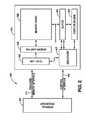
- the memory device 34may also include an internal processor, such as a compute engine 38 , which may include one or more arithmetic logic units (ALUs). Further, the compute engine 38 may refer to a plurality of compute engines 38 on the memory device 34 . The compute engine 38 may be configured to perform operations on data. In one embodiment, the compute engine 38 may include one or more ALU blocks configured to perform various mathematical or logical operations on data, such as operands or intermediate results of previous operations.
- ALUsarithmetic logic units
- the compute engine 38may be controlled by a sequencer 40 , which may be capable of accessing the memory array 36 , including retrieving information (e.g., reading instructions and/or data) from, and storing information (e.g., writing completed results) in the memory array 36 .
- the process of retrieving and storing informationmay also involve a fetch unit 50 , a memory control 48 , and a memory component, such as the buffer 42 .
- the sequencer 40may transfer command information and the data address to the fetch unit 50 , and the fetch unit 50 may sequence the memory array 36 states to read and write data.
- the memory control 48may decode the command and address bits received by the fetch unit 50 from the sequencer 40 .
- the resultsmay be stored in the buffer 42 before they are written to the memory array 36 .
- intermediate resultsmay also be stored in memory components in the memory device 34 .
- intermediate resultsmay be stored in memory components such as the buffer 42 or memory registers coupled to the compute engine 38 .
- a compute engine 38may access the buffer 42 for the intermediate results to perform subsequent operations.
- the buffer 42may include one or more layer of buffers.
- the buffer 42may include a compute buffer 54 , which may store data (e.g., operands, intermediate results, completed results, etc.), and an instruction buffer, which may store instructions transferred from the memory array 36 .
- the buffer 42may also include additional buffers, such as a data buffer or a simple buffer, which may provide denser storage, and may store intermediate or final results of executed instructions.
- buffer 42may refer to any type of buffer layer (e.g., a compute buffer, instruction buffer, data buffer, etc.), or any type of memory capable of holding data and/or instructions transferred to and from the compute engine 38 .
- memories having internal processorshave improved processing capabilities because internal communication within a memory, e.g., between an internal processor and a memory array, may reduce power consumption and processing time.
- the memory systems 30 having memory devices 34 configured to substantially process instructions within the memory device 34may further improve processing capabilities. More specifically, the memory device 34 may be configured to arbitrate access to the memory array 36 on the device 34 .
- a process for arbitrating memory array accessmay be depicted in the memory device portion 52 of FIG. 3 , which illustrates possible communications between different components of the memory device portion 52 . Furthermore, a process 80 for arbitrating memory array access in a memory device 34 may also be explained in the flow chart of FIG. 4 . As FIG. 4 may explain memory device components and communications depicted in FIG. 3 , FIGS. 3 and 4 may be discussed concurrently.
- the process 80may start when the sequencer 40 fetches an instruction from an instruction buffer 56 (block 82 ).
- the instructionmay have been transferred to the memory array 36 externally, such as by an external processor 32 (as in FIG. 2 ), and buffered in the instruction buffer 56 .
- the instructionmay include operations to be performed on data, commands to either read or write data to the memory array 36 , as well as data addresses (e.g., the bank and page in the memory array 36 where the data is located).
- the sequencermay retrieve an instruction by sending a control signal 58 to the instruction buffer 56 to identify the rows in the instruction buffer from which the instructions are to be retrieved.
- the instructionsmay be transferred (path 60 ) to the sequencer 40 .
- the instructionsmay be either direct or indirect.
- a direct instructionmay include multiple commands, such as commands for organizing the operations to be performed on the data, commands for reading or writing the data, and/or addresses of the data.
- direct instructionsmay include commands to read or write data from the memory array 36 , addresses in the memory array 36 for the data (e.g., where to read operand A and an operand B), as well as commands which tell the sequencer 40 how to organize certain operations for the operands A and B.
- An indirect instructionmay include comparatively simpler commands, which may be transferred to the sequencer 40 one command at a time.
- an indirect instructionmay include one command to fetch an operand A from the memory array 36 , another command to fetch an operand B from the memory array 36 , a third command to organize certain operations for the operands A and B, and a fourth command used to identify an address in the array 36 where completed results may be stored.
- direct instructionsmay increase processing speed, as all parts of a direct instruction (e.g., the different commands of the indirect instruction) are transferred together, indirect instructions may enable a simpler memory device 34 .
- the sequencer 40may be simpler, the bus 60 may not need to be as wide, and/or the instruction buffer 56 may not need to be as wide as an instruction buffer 56 transferring direct instructions.
- the instructions transferred by the instruction buffer 56may include commands to read data (e.g., operands) from or write data (e.g., completed results) to the memory array 36 .
- the instructionsmay command the sequencer 40 to retrieve certain operands stored at some address (e.g., a particular bank and row) in the array 36 .
- the instructionsmay include the address of intermediate results to be retrieved from the compute buffer 42 . If the instructions are executed using intermediate results, the sequencer 40 may not need to access the memory array 36 .
- access to the array 36may be arbitrated to prevent corruption of the memory array 36 , which may occur if more than one command (e.g., reading and writing) are occurring within the same bank of the array 36 at once.
- the memory device 34may be configured such that arbitration of memory array access may be performed within the memory device 34 .
- the sequencer 40may control memory array arbitration, and may communicate externally (e.g., with the external processor 32 ) to arbitrate memory array access. However, communication with external devices may be substantially reduced. For example, access to the memory array 36 may be substantially controlled by the fetch unit 50 in the memory device 34 .
- the process 80depicts memory array access that is substantially controlled by the fetch unit 50 .
- the sequencer 40may transfer the instructions, including the command 62 and the address 64 to the fetch unit 50 (block 84 ).
- the fetch unit 50may transfer the commands 62 and addresses 64 to the memory control 48 , which decodes the instructions into the decoded address 68 and the control signal 66 (block 86 ).
- the decoded address 68 and control signal 66may command the reading or writing of data from the proper addresses (e.g., a certain bank, page, and/or row).
- the fetch unit 50may then activate (e.g., open) the bank holding the data or the bank to which data is to be written (block 90 ).
- the fetch unit 50may substantially control access to the memory array to prevent more than one command (e.g., reading or writing data) from being performed on the same bank of the memory array 36 .
- Such arbitration of accessing the memory array 36may have various implementations in accordance with the present techniques.
- the memory array 36may include control logic 74 , which may be configured to monitor when a page in the array 36 is open or closed.
- the control logic 74may engage in “handshaking,” which may refer to sending a control signal 76 to the fetch unit 50 indicating a status of a bank of interest (i.e., the bank to which the fetch unit 50 is commanded to read from or write to).
- the fetch unit 50may wait for the signal 76 before performing commands on the bank of interest (block 90 ).
- the fetch unit 50may perform the command(s) of reading from and/or writing to the bank of interest (block 92 ). If the instructions received at the sequencer 40 included commands to read data, the fetch unit may retrieve the data from the bank of interest and transfer the data to the compute buffer 54 , such that the data will be available for a compute engine 38 to execute instructions on the data. Further, if the instructions received at the sequencer 40 include commands to write data to the memory array, the fetch unit 50 may write the data (e.g., completed results) at the commanded address in the memory array 36 .
- the control logic 74 of the memory array 36may send a signal 76 to the fetch unit 50 to indicate that the commands have been performed on the bank of interest (block 94 ).
- the fetch unit 50may then precharge (e.g., close) the bank of interest on the memory array 36 (block 96 ), and the control logic 74 may send a signal 74 acknowledging that the bank of interest has been closed (block 98 ).
- the fetch unit 50may send a signal 78 indicating to the sequencer 40 that the command has been performed, and that the data has been either retrieved or stored to the proper address(es) in the memory array 36 (block 100 ).
- the datamay be transferred (path 70 ) to the compute buffer 54 , which may hold the data until the compute engine 38 (as in FIG. 2 , not depicted in FIG. 3 ) uses the data to execute instructions.
- the fetch unit 50may time the performance of commands (e.g., reading or writing) based on timers 79 .
- the timers 79may be based on clock cycles of how long data transfers to and from the memory array 36 typically take. For example, after a bank is open in the memory array (block 88 ) and before performing commands on the bank, a timer 79 may be activated, and the fetch unit 50 may wait until the time conditions set by the timer 79 are met to ensure that no other commands are being performed on the bank of interest (block 90 ). Once the timer conditions are met, the fetch unit 50 may begin to read from or write to the bank of interest (block 92 ).
- timer 79may be activated when the fetch unit begins to perform a command on a bank, based on when the command is estimated to complete. Future accesses to that bank may be based on the activated timer 79 from the previous command.
- timers 79such as tRCD, tRP, etc. may be used to set an appropriate amount of time before the fetch unit 50 performs commands or closes the bank of interest.
- the sequencer 40may also receive instructions which do not include accessing the memory array 36 .
- the sequencer 40may receive instructions which may be executed using intermediate results of previous operations or instructions, which may already be buffered in some row of the compute buffer 54 .
- the sequencer 40may send a control signal 72 to the compute buffer 54 to identify the row(s) in the compute buffer 54 on which the intermediate results are located.
- transfers between the compute buffer 54 and the memory array 36may not occur for performing operations where operands are already buffered in the compute buffer 54 as intermediate results from previous operations.
- the buffer 42may include one or more layers, which may be partitioned and/or have different busses to components of the memory device 34 .
- the buffer 42may include an instruction buffer 56 and a compute buffer 54 , which are illustrated in FIG. 3 as separate buffers 42 , each having individual buses to the sequencer 40 and the memory array 36 .
- the separate buffers 54 and 56 in FIG. 3may also be one buffer 42 having layers for storing data and instructions, and having a shared bus between the buffer 42 (e.g., combined buffers 54 and 56 ) and the memory array 36 and/or the sequencer 40 .
Landscapes
- Engineering & Computer Science (AREA)
- Theoretical Computer Science (AREA)
- Human Computer Interaction (AREA)
- Physics & Mathematics (AREA)
- General Engineering & Computer Science (AREA)
- General Physics & Mathematics (AREA)
- Microelectronics & Electronic Packaging (AREA)
- Memory System (AREA)
- Advance Control (AREA)
- Multi Processors (AREA)
- Memory System Of A Hierarchy Structure (AREA)
Abstract
Description
- This application is a continuation of and claims priority to U.S. patent application Ser. No. 12/603,393, which was filed on Oct. 21, 2009, now U.S. Pat. No. 8,719,516, which issued May 6, 2014 and is herein incorporated by reference.
- 1. Field of Invention
- Embodiments of the invention relate generally to memory systems, and more particularly, to memory systems having internal processors.
- 2. Description of Related Art
- This section is intended to introduce the reader to various aspects of art that may be related to various aspects of the present invention, which are described and/or claimed below. This discussion is believed to be helpful in providing the reader with background information to facilitate a better understanding of the various aspects of the present invention. Accordingly, it should be understood that these statements are to be read in this light and not as admissions of prior art.
- Electronic systems typically include one or more processors, which may retrieve and execute instructions, and store the results of the executed instruction, such as to store the results to a suitable location. A processor may generally use arithmetic logic unit (ALU) circuitry to execute instructions, such as arithmetic and logic operations, on data, such as one or more operands. For example, the ALU circuitry may add, subtract, multiply, or divide one operand from another, or may subject one or more operands to logic operations, such as AND, OR, XOR, and NOT logic functions. A processor may execute instructions having different degrees of complexity, and different instructions may involve inputting the operand(s) through the ALU circuitry in one or multiple clock cycles.
- A number of components in the electronic system may be involved in directing a set of instructions to the ALU for execution. In some devices, the instructions may be generated by a controller, or some other suitable processor in the electronic system. Data (e.g., the operands on which the instructions will be executed, as well as the instructions) may be stored in a memory component (e.g., a memory array) that is accessible by the ALU. The instructions and data may be retrieved from the memory and sequenced and/or buffered before the ALU begins to execute instructions on the data. Furthermore, as different types of operations may be executed in one or multiple clock cycles through the ALU, intermediate results of the instructions and/or data may also be sequenced and/or buffered.
- Typically, a processor (e.g., the ALU circuitry) may be external to the memory array, and data must be accessed via a bus between the processor and the memory array to execute a set of instructions. As processing speed may be limited by the bandwidth of the bus, processing performance may be improved in a processor-in-memory (PIM) device, where the processor is implemented internal to a memory (e.g., directly on the memory), conserving time and power in processing. Furthermore, the memory may also be configured to execute instructions with little or no external assistance, further saving on processing power.
- Certain embodiments are described in the following detailed description and in reference to the drawings in which:
FIG. 1 depicts a block diagram of a processor-based system in accordance with an embodiment of the present technique;FIG. 2 depicts a block diagram of a memory system having an internal processor interfaced with an external processor, in accordance with an embodiment of the present technique;FIG. 3 illustrates a portion of a memory having an internal processor and communication pathways between different components of the memory, in accordance with one or more embodiments of the present technique; andFIG. 4 is a flow chart depicting a process for accessing a memory array in a memory having an internal processor, in accordance with one or more embodiments of the present technique.- An electronic device may generally use a processor to process instructions in multiple stages. Processing the instructions may include executing the instructions, and storing the results of the executed instructions. For example, instructions, and the data on which the instructions will be executed, may be sent by an external processor (e.g., a memory controller) to an internal processor (e.g., ALU circuitry). The instructions and/or data may first be stored in a memory array to be retrieved when the internal processor is available to execute the instructions. Once the instruction(s) have been executed, the internal processor may store the results of the instruction(s) in a memory component, the memory array, or to any other suitable output.
- A processor that is external to the memory may require an external bus to transfer information (e.g., instructions and/or data) to and from the memory array. Processing efficiency may be partly limited by the bandwidth of the external bus, as transferring information between a memory array and a processor may consume power and time. In one or more embodiments, a memory may conserve power by allowing information to be transferred between the memory array and a processor without an external bus.
- In accordance with the present techniques, one or more processors, such as ALUs, may be packaged with a memory component in the memory. For example, the memory may be a processor-in-memory (PIM), and may include ALUs embedded on a memory device (e.g., a memory array), which may store instructions and data to be executed by the ALUs and the results from the executed instructions. In other embodiments, the ALUs and the memory array may be on unique dies in the same package. For example, the ALUs and the memory array may be arranged in a multi-chip package (MCP), and may be electrically connected by one or more through-silicon vias (TSVs). Processors which are packaged with a memory device (whether embedded on a memory device or as part of a MCP, for example), may be referred to as “internal processors,” and thus a memory device packaged with a processor may be considered a memory “having” an internal processor. As used herein, a “compute engine” may be an example of an internal processor, and may be packaged with a memory device in accordance with the present techniques. Further, an internal processor, such as a compute engine, may comprise one or more ALUs.
- The memory may also include components such as a sequencer to organize the instructions and data, a fetch unit to access data from the memory array, and a buffer to store (e.g., hold) data and/or instructions. The buffer may also hold intermediate results or final results before they are transferred to the memory array. In one embodiment, the sequencer may arbitrate access to the memory array, or may communicate with a processor external to the memory (i.e., an external processor) which arbitrates access to the array. In one or more embodiments, the fetch unit may also arbitrate access to the memory array. Internal arbitration of the memory array on the memory may enable the memory to process instructions with little or no assistance from external devices, such as external processors.
- One embodiment of the present technique involves a memory configured to process instructions with reduced communication with other devices or processors external to the memory. More specifically, certain components, such as a sequencer and a fetch unit, may read and write data and organize the performance of operations with substantially no external control or external data transfer. Decreasing the amount of external communication may allow a memory to have fewer external bus lines, or external bus lines with reduced widths. Further, decreasing the amount of external communication may reduce processing power, as power-consuming data transfers into and out of the memory may be saved.
- Now turning to the figures,
FIG. 1 depicts a processor-based system, generally designated byreference numeral 10. As is explained below, thesystem 10 may include various electronic devices manufactured in accordance with embodiments of the present technique. Thesystem 10 may be any of a variety of types such as a computer, pager, cellular phone, personal organizer, control circuit, etc. In a typical processor-based system, one ormore processors 12, such as a microprocessor, control the processing of system functions and requests in thesystem 10. As is explained below, theprocessor 12 and other subcomponents of thesystem 10 may include memory manufactured in accordance with one or more embodiments of the present technique. - The
system 10 typically includes apower supply 14. For instance, if thesystem 10 is a portable system, thepower supply 14 may advantageously include a fuel cell, a power scavenging device, permanent batteries, replaceable batteries, and/or rechargeable batteries. Thepower supply 14 may also include an AC adapter, so thesystem 10 may be plugged into a wall outlet, for instance. Thepower supply 14 may also include a DC adapter such that thesystem 10 may be plugged into a vehicle cigarette lighter, for instance. - Various other devices may be coupled to the
processor 12 depending on the functions that thesystem 10 performs. For instance, aninput device 16 may be coupled to theprocessor 12. Theinput device 16 may include buttons, switches, a keyboard, a light pen, a mouse, a digitizer and stylus, and/or a voice recognition system, for instance. Adisplay 18 may also be coupled to theprocessor 12. Theinput device 16 and/or thedisplay 18 may each or both form a user interface. Thedisplay 18 may include an LCD, an SED display, a CRT display, a DLP display, a plasma display, an OLED display, LEDs, and/or an audio display, for example. Furthermore, an RF sub-system/baseband processor 20 may also be coupled to theprocessor 12. The RF sub-system/baseband processor 20 may include an antenna that is coupled to an RF receiver and to an RF transmitter (not shown). One ormore communication ports 22 may also be coupled to theprocessor 12. Thecommunication port 22 may be adapted to be coupled to one or moreperipheral devices 24 such as a modem, a printer, a computer, or to a network, such as a local area network, remote area network, intranet, or the Internet, for instance. - The
processor 12 generally controls thesystem 10 by processing programs stored in the memory. The software programs may include an operating system, database software, drafting software, word processing software, and/or video, photo, or sound editing software, for example. The memory is operably coupled to theprocessor 12 to store and facilitate execution of instructions to implement various programs. For instance, theprocessor 12 may be coupled to thesystem memory 26, which may include dynamic random access memory (DRAM), and/or synchronous dynamic random access memory (SDRAM). Thesystem memory 26 may include volatile memory, non-volatile memory, or a combination thereof. Thesystem memory 26 is typically large so that it can store dynamically loaded applications and data. - The
processor 12 may also be coupled tonon-volatile memory 28, which is not to suggest thatsystem memory 26 is necessarily volatile. Thenon-volatile memory 28 may include read-only memory (ROM), such as an EPROM, resistive read-only memory (RROM), and/or flash memory to be used in conjunction with thesystem memory 26. The size of the ROM is typically selected to be just large enough to store any necessary operating system, application programs, and fixed data. Additionally, thenon-volatile memory 28 may include a high capacity memory such as a tape or disk drive memory, such as a hybrid-drive including resistive memory or other types of non-volatile solid-state memory, for instance. - Some embodiments of the present technique involve communication between the
processor 12 and components of thesystem memory 26. For example, theprocessor 12 may include a general purpose processor, a central processing unit, a processor core, an ASIC, a memory controller, and/or an ALU, for example, capable of sending and receiving signals from internal processors of memory, such as memory devices in thesystem memory 26. Components of thesystem 10 involved in the communication between theprocessor 12 and the components of a memory such assystem memory 26 may be generally referred to as a “memory system”30, as illustrated in the block diagram ofFIG. 2 . In some embodiments, amemory system 30 may include amemory device 34, which may be part of thesystem memory 26 of the system10 (as inFIG. 1 ) and may have an internal processor such as thecompute engine 38. Thememory system 30 may also include anexternal processor 32, which may be in a system-on-a-chip (SOC) with a more general purpose processor to collectively form aprocessor 12 of a processor-controlled system10 (as inFIG. 1 ). Theexternal processor 32, which may also be an external memory controller, may communicate with and/or control certain components of amemory device 34. - The
memory system 30 may include components which have functions that are not limited to the communication between theexternal processor 32 and thememory device 32. For example, theexternal processor 32 may control devices in addition to thememory device 34. However, theexternal processor 32, as explained with respect to thememory system 30, may refer to one function of theexternal processor 32 which communicates with and/or controls certain components of thememory device 34. Likewise, not all parts of thesystem memory 26 may be part of thememory system 30. The “memory device”34 may refer to components of the memory system involved in the communication with theexternal processor 32, in accordance with the present techniques. - The
external processor 32 and thememory device 34 may be operably coupled by astandard memory interface 44 which may allow data transfer between theexternal processor 32 and thememory device 34, and may allow theexternal processor 32 to send (e.g., transfer) commands to thememory device 34. In one or more embodiments, the types ofstandard memory interface 44 may include DDR, DDR2, DDR3, LPDDR, or LPDDR2, for example. Further, in some embodiments, an additional interface(s) may be configured to allow the transfer of data, and also commands (e.g., requests, grants, instructions, etc.), between thememory device 34 and theexternal processor 32. For example, theexternal processor 32 and thememory device 34 may also be operably coupled by acontrol interface 46, which may allow the transfer of commands between theexternal processor 32 and thememory device 34, including commands from thememory device 34 to theexternal processor 32. - A memory, such as a
memory device 34, may be configured to substantially process instructions (including executing the instructions and storing the completed results) may have reduced communication with theexternal processor 32. While access to amemory array 36 on thememory device 34 may typically be controlled by theexternal processor 32, in one or more embodiments, the processing of instructions, including memory array access, may be substantially controlled within thememory device 34. For example, once theexternal processor 32 sends instructions to thememory array 36, the processing of the instructions, including accessing thememory array 34 to read and/or write data, may occur largely within thememory device 34. - The
memory array 36, which may refer to any suitable form of storage, and may include, for example, a DRAM array or an SDRAM array. In one or more embodiments, thememory array 36 may store data, instructions to be executed on the data, and completed results of executed instructions. Thememory array 36 may be accessed by certain components in thememory system 30, which may access the array to read instructions and/or data, write completed results, etc. Typically, only one command (e.g., reading and/or writing) may be performed in a bank of thememory array 36 at one time. Thus, access to thememory array 36 may be arbitrated such that commands in memory array banks do not conflict. - The
memory device 34 may also include an internal processor, such as acompute engine 38, which may include one or more arithmetic logic units (ALUs). Further, thecompute engine 38 may refer to a plurality ofcompute engines 38 on thememory device 34. Thecompute engine 38 may be configured to perform operations on data. In one embodiment, thecompute engine 38 may include one or more ALU blocks configured to perform various mathematical or logical operations on data, such as operands or intermediate results of previous operations. - The
compute engine 38 may be controlled by asequencer 40, which may be capable of accessing thememory array 36, including retrieving information (e.g., reading instructions and/or data) from, and storing information (e.g., writing completed results) in thememory array 36. The process of retrieving and storing information may also involve a fetchunit 50, amemory control 48, and a memory component, such as thebuffer 42. Thesequencer 40 may transfer command information and the data address to the fetchunit 50, and the fetchunit 50 may sequence thememory array 36 states to read and write data. In one embodiment, thememory control 48 may decode the command and address bits received by the fetchunit 50 from thesequencer 40. - Once the
compute engine 38 has executed the instructions, the results may be stored in thebuffer 42 before they are written to thememory array 36. Further, as some instructions may require more than one clock cycle in the compute engine and/or require multiple operations to be performed, intermediate results may also be stored in memory components in thememory device 34. For example, intermediate results may be stored in memory components such as thebuffer 42 or memory registers coupled to thecompute engine 38. In one or more embodiments, acompute engine 38 may access thebuffer 42 for the intermediate results to perform subsequent operations. - The
buffer 42 may include one or more layer of buffers. For example, and as will be further discussed with reference toFIG. 3 , thebuffer 42 may include acompute buffer 54, which may store data (e.g., operands, intermediate results, completed results, etc.), and an instruction buffer, which may store instructions transferred from thememory array 36. Thebuffer 42 may also include additional buffers, such as a data buffer or a simple buffer, which may provide denser storage, and may store intermediate or final results of executed instructions. As used herein, “buffer 42” may refer to any type of buffer layer (e.g., a compute buffer, instruction buffer, data buffer, etc.), or any type of memory capable of holding data and/or instructions transferred to and from thecompute engine 38. - As discussed, memories having internal processors have improved processing capabilities because internal communication within a memory, e.g., between an internal processor and a memory array, may reduce power consumption and processing time. In one or more embodiments, the
memory systems 30 havingmemory devices 34 configured to substantially process instructions within thememory device 34 may further improve processing capabilities. More specifically, thememory device 34 may be configured to arbitrate access to thememory array 36 on thedevice 34. - A process for arbitrating memory array access may be depicted in the
memory device portion 52 ofFIG. 3 , which illustrates possible communications between different components of thememory device portion 52. Furthermore, aprocess 80 for arbitrating memory array access in amemory device 34 may also be explained in the flow chart ofFIG. 4 . AsFIG. 4 may explain memory device components and communications depicted inFIG. 3 ,FIGS. 3 and 4 may be discussed concurrently. - The
process 80 may start when thesequencer 40 fetches an instruction from an instruction buffer56 (block82). In one embodiment, the instruction may have been transferred to thememory array 36 externally, such as by an external processor32 (as inFIG. 2 ), and buffered in theinstruction buffer 56. The instruction the may include operations to be performed on data, commands to either read or write data to thememory array 36, as well as data addresses (e.g., the bank and page in thememory array 36 where the data is located). The sequencer may retrieve an instruction by sending acontrol signal 58 to theinstruction buffer 56 to identify the rows in the instruction buffer from which the instructions are to be retrieved. The instructions may be transferred (path60) to thesequencer 40. - In one or more embodiments, the instructions may be either direct or indirect. A direct instruction may include multiple commands, such as commands for organizing the operations to be performed on the data, commands for reading or writing the data, and/or addresses of the data. For example, direct instructions may include commands to read or write data from the
memory array 36, addresses in thememory array 36 for the data (e.g., where to read operand A and an operand B), as well as commands which tell thesequencer 40 how to organize certain operations for the operands A and B. An indirect instruction may include comparatively simpler commands, which may be transferred to thesequencer 40 one command at a time. For example, an indirect instruction may include one command to fetch an operand A from thememory array 36, another command to fetch an operand B from thememory array 36, a third command to organize certain operations for the operands A and B, and a fourth command used to identify an address in thearray 36 where completed results may be stored. While direct instructions may increase processing speed, as all parts of a direct instruction (e.g., the different commands of the indirect instruction) are transferred together, indirect instructions may enable asimpler memory device 34. For example, in amemory device 34 configured to transfer indirect instructions, thesequencer 40 may be simpler, thebus 60 may not need to be as wide, and/or theinstruction buffer 56 may not need to be as wide as aninstruction buffer 56 transferring direct instructions. - The instructions transferred by the
instruction buffer 56 may include commands to read data (e.g., operands) from or write data (e.g., completed results) to thememory array 36. For example, the instructions may command thesequencer 40 to retrieve certain operands stored at some address (e.g., a particular bank and row) in thearray 36. Alternatively, as some instructions may be executed using intermediate results of previous operations, the instructions may include the address of intermediate results to be retrieved from thecompute buffer 42. If the instructions are executed using intermediate results, thesequencer 40 may not need to access thememory array 36. - If the instructions command the
sequencer 40 to access operands that are stored in thememory array 36, access to thearray 36 may be arbitrated to prevent corruption of thememory array 36, which may occur if more than one command (e.g., reading and writing) are occurring within the same bank of thearray 36 at once. In one or more embodiments, thememory device 34 may be configured such that arbitration of memory array access may be performed within thememory device 34. In one embodiment, thesequencer 40 may control memory array arbitration, and may communicate externally (e.g., with the external processor32) to arbitrate memory array access. However, communication with external devices may be substantially reduced. For example, access to thememory array 36 may be substantially controlled by the fetchunit 50 in thememory device 34. - The
process 80 depicts memory array access that is substantially controlled by the fetchunit 50. Once thesequencer 40 receives the instructions, thesequencer 40 may transfer the instructions, including thecommand 62 and theaddress 64 to the fetch unit50 (block84). In one embodiment, the fetchunit 50 may transfer thecommands 62 and addresses64 to thememory control 48, which decodes the instructions into the decodedaddress 68 and the control signal66 (block86). The decodedaddress 68 andcontrol signal 66 may command the reading or writing of data from the proper addresses (e.g., a certain bank, page, and/or row). The fetchunit 50 may then activate (e.g., open) the bank holding the data or the bank to which data is to be written (block90). - The fetch
unit 50 may substantially control access to the memory array to prevent more than one command (e.g., reading or writing data) from being performed on the same bank of thememory array 36. Such arbitration of accessing thememory array 36 may have various implementations in accordance with the present techniques. In one embodiment, thememory array 36 may includecontrol logic 74, which may be configured to monitor when a page in thearray 36 is open or closed. Thecontrol logic 74 may engage in “handshaking,” which may refer to sending acontrol signal 76 to the fetchunit 50 indicating a status of a bank of interest (i.e., the bank to which the fetchunit 50 is commanded to read from or write to). The fetchunit 50 may wait for thesignal 76 before performing commands on the bank of interest (block90). - If the bank of interest is available (e.g., commands are not being performed on the bank of interest), the fetch
unit 50 may perform the command(s) of reading from and/or writing to the bank of interest (block92). If the instructions received at thesequencer 40 included commands to read data, the fetch unit may retrieve the data from the bank of interest and transfer the data to thecompute buffer 54, such that the data will be available for acompute engine 38 to execute instructions on the data. Further, if the instructions received at thesequencer 40 include commands to write data to the memory array, the fetchunit 50 may write the data (e.g., completed results) at the commanded address in thememory array 36. - Once the commands are performed (block92), the
control logic 74 of thememory array 36 may send asignal 76 to the fetchunit 50 to indicate that the commands have been performed on the bank of interest (block94). The fetchunit 50 may then precharge (e.g., close) the bank of interest on the memory array36 (block96), and thecontrol logic 74 may send asignal 74 acknowledging that the bank of interest has been closed (block98). The fetchunit 50 may send asignal 78 indicating to thesequencer 40 that the command has been performed, and that the data has been either retrieved or stored to the proper address(es) in the memory array36 (block100). The data may be transferred (path70) to thecompute buffer 54, which may hold the data until the compute engine38 (as inFIG. 2 , not depicted inFIG. 3 ) uses the data to execute instructions. - As discussed, different implementations may be used for arbitration of memory array access. In another embodiment, the fetch
unit 50 may time the performance of commands (e.g., reading or writing) based ontimers 79. Thetimers 79 may be based on clock cycles of how long data transfers to and from thememory array 36 typically take. For example, after a bank is open in the memory array (block88) and before performing commands on the bank, atimer 79 may be activated, and the fetchunit 50 may wait until the time conditions set by thetimer 79 are met to ensure that no other commands are being performed on the bank of interest (block90). Once the timer conditions are met, the fetchunit 50 may begin to read from or write to the bank of interest (block92). Based on the command to be performed, another timer may be set to indicate when the command would complete. The fetchunit 50 may wait for the command completion timer to be met before precharging (closing) the bank in thememory array 36. Furthermore, in one embodiment, atimer 79 may be activated when the fetch unit begins to perform a command on a bank, based on when the command is estimated to complete. Future accesses to that bank may be based on the activatedtimer 79 from the previous command. In one or more embodiments,timers 79 such as tRCD, tRP, etc. may be used to set an appropriate amount of time before the fetchunit 50 performs commands or closes the bank of interest. - While the
process 80 explains the processing of instructions which include reading and/or writing to thememory array 36, thesequencer 40 may also receive instructions which do not include accessing thememory array 36. For example, thesequencer 40 may receive instructions which may be executed using intermediate results of previous operations or instructions, which may already be buffered in some row of thecompute buffer 54. Rather than performing the previously discussedprocess 80, thesequencer 40 may send acontrol signal 72 to thecompute buffer 54 to identify the row(s) in thecompute buffer 54 on which the intermediate results are located. As the data is already in thecompute buffer 54, transfers between thecompute buffer 54 and thememory array 36 may not occur for performing operations where operands are already buffered in thecompute buffer 54 as intermediate results from previous operations. - Furthermore, as discussed, the buffer42 (as in
FIG. 2 ) may include one or more layers, which may be partitioned and/or have different busses to components of thememory device 34. Thebuffer 42 may include aninstruction buffer 56 and acompute buffer 54, which are illustrated inFIG. 3 asseparate buffers 42, each having individual buses to thesequencer 40 and thememory array 36. However, theseparate buffers FIG. 3 may also be onebuffer 42 having layers for storing data and instructions, and having a shared bus between the buffer42 (e.g., combinedbuffers 54 and56) and thememory array 36 and/or thesequencer 40. - While the invention may be susceptible to various modifications and alternative forms, specific embodiments have been shown by way of example in the drawings and have been described in detail herein. However, it should be understood that the invention is not intended to be limited to the particular forms disclosed. Rather, the invention is to cover all modifications, equivalents, and alternatives falling within the spirit and scope of the invention as defined by the following appended claims.
Claims (20)
Priority Applications (1)
| Application Number | Priority Date | Filing Date | Title |
|---|---|---|---|
| US14/269,873US9164698B2 (en) | 2009-10-21 | 2014-05-05 | Memory having internal processors and methods of controlling memory access |
Applications Claiming Priority (2)
| Application Number | Priority Date | Filing Date | Title |
|---|---|---|---|
| US12/603,393US8719516B2 (en) | 2009-10-21 | 2009-10-21 | Memory having internal processors and methods of controlling memory access |
| US14/269,873US9164698B2 (en) | 2009-10-21 | 2014-05-05 | Memory having internal processors and methods of controlling memory access |
Related Parent Applications (1)
| Application Number | Title | Priority Date | Filing Date |
|---|---|---|---|
| US12/603,393ContinuationUS8719516B2 (en) | 2009-10-21 | 2009-10-21 | Memory having internal processors and methods of controlling memory access |
Publications (2)
| Publication Number | Publication Date |
|---|---|
| US20140244948A1true US20140244948A1 (en) | 2014-08-28 |
| US9164698B2 US9164698B2 (en) | 2015-10-20 |
Family
ID=43447261
Family Applications (2)
| Application Number | Title | Priority Date | Filing Date |
|---|---|---|---|
| US12/603,393Active2031-04-21US8719516B2 (en) | 2009-10-21 | 2009-10-21 | Memory having internal processors and methods of controlling memory access |
| US14/269,873ActiveUS9164698B2 (en) | 2009-10-21 | 2014-05-05 | Memory having internal processors and methods of controlling memory access |
Family Applications Before (1)
| Application Number | Title | Priority Date | Filing Date |
|---|---|---|---|
| US12/603,393Active2031-04-21US8719516B2 (en) | 2009-10-21 | 2009-10-21 | Memory having internal processors and methods of controlling memory access |
Country Status (6)
| Country | Link |
|---|---|
| US (2) | US8719516B2 (en) |
| EP (1) | EP2491561B1 (en) |
| KR (1) | KR101354346B1 (en) |
| CN (1) | CN102640226B (en) |
| TW (1) | TWI442244B (en) |
| WO (1) | WO2011049753A1 (en) |
Cited By (6)
| Publication number | Priority date | Publication date | Assignee | Title |
|---|---|---|---|---|
| WO2017065379A1 (en)* | 2015-10-16 | 2017-04-20 | 삼성전자 주식회사 | Method and apparatus for processing instructions using processing-in-memory |
| WO2017155781A1 (en)* | 2016-03-10 | 2017-09-14 | Micron Technology, Inc. | Apparatuses and methods for logic/memory devices |
| US10346092B2 (en) | 2017-08-31 | 2019-07-09 | Micron Technology, Inc. | Apparatuses and methods for in-memory operations using timing circuitry |
| US10416927B2 (en) | 2017-08-31 | 2019-09-17 | Micron Technology, Inc. | Processing in memory |
| US10553260B2 (en) | 2017-09-27 | 2020-02-04 | Samsung Electronics Co., Ltd. | Stacked memory device, a system including the same and an associated method |
| US10741239B2 (en) | 2017-08-31 | 2020-08-11 | Micron Technology, Inc. | Processing in memory device including a row address strobe manager |
Families Citing this family (38)
| Publication number | Priority date | Publication date | Assignee | Title |
|---|---|---|---|---|
| US8281395B2 (en)* | 2009-01-07 | 2012-10-02 | Micron Technology, Inc. | Pattern-recognition processor with matching-data reporting module |
| US8521958B2 (en) | 2009-06-04 | 2013-08-27 | Micron Technology, Inc. | Internal processor buffer |
| US8234460B2 (en) | 2009-06-04 | 2012-07-31 | Micron Technology, Inc. | Communication between internal and external processors |
| US8380916B2 (en) | 2009-06-04 | 2013-02-19 | Micron Technology, Inc. | Control of page access in memory |
| US9535876B2 (en) | 2009-06-04 | 2017-01-03 | Micron Technology, Inc. | Conditional operation in an internal processor of a memory device |
| US9477636B2 (en) | 2009-10-21 | 2016-10-25 | Micron Technology, Inc. | Memory having internal processors and data communication methods in memory |
| TWI631459B (en)* | 2011-11-04 | 2018-08-01 | 曾銘松 | Memory device and its operation method |
| US9733847B2 (en) | 2014-06-02 | 2017-08-15 | Micron Technology, Inc. | Systems and methods for transmitting packets in a scalable memory system protocol |
| US10061590B2 (en)* | 2015-01-07 | 2018-08-28 | Micron Technology, Inc. | Generating and executing a control flow |
| CN107408404B (en)* | 2015-02-06 | 2021-02-12 | 美光科技公司 | Apparatus and methods for memory devices as storage of program instructions |
| FR3032814B1 (en)* | 2015-02-18 | 2018-02-02 | Upmem | DRAM CIRCUIT WITH INTEGRATED PROCESSOR |
| KR20170060739A (en) | 2015-11-25 | 2017-06-02 | 삼성전자주식회사 | Semiconductor memory device and memory system including the same |
| KR102548591B1 (en)* | 2016-05-30 | 2023-06-29 | 삼성전자주식회사 | Semiconductor memory device and operation method thereof |
| KR20170136829A (en) | 2016-06-02 | 2017-12-12 | 삼성전자주식회사 | Semiconductor Device, Memory Device and Method of Operating Memory Device |
| US10423353B2 (en)* | 2016-11-11 | 2019-09-24 | Micron Technology, Inc. | Apparatuses and methods for memory alignment |
| KR20180093648A (en)* | 2017-02-14 | 2018-08-22 | 에스케이하이닉스 주식회사 | Storage device and operating method thereof |
| US10684955B2 (en)* | 2017-04-21 | 2020-06-16 | Micron Technology, Inc. | Memory devices and methods which may facilitate tensor memory access with memory maps based on memory operations |
| US10236038B2 (en)* | 2017-05-15 | 2019-03-19 | Micron Technology, Inc. | Bank to bank data transfer |
| US10866900B2 (en) | 2017-10-17 | 2020-12-15 | Samsung Electronics Co., Ltd. | ISA extension for high-bandwidth memory |
| US10825491B2 (en)* | 2017-12-11 | 2020-11-03 | Micron Technology, Inc. | Systems and methods for writing zeros to a memory array |
| WO2019202371A1 (en)* | 2018-04-16 | 2019-10-24 | Badenhorst Emile | A processor and a method of operating a processor |
| US10956315B2 (en) | 2018-07-24 | 2021-03-23 | Micron Technology, Inc. | Memory devices and methods which may facilitate tensor memory access |
| KR102665410B1 (en) | 2018-07-30 | 2024-05-13 | 삼성전자주식회사 | Performing internal processing operations of memory device |
| TWI749331B (en)* | 2018-10-11 | 2021-12-11 | 力晶積成電子製造股份有限公司 | Memory with processing in memory architecture and operating method thereof |
| US10483978B1 (en)* | 2018-10-16 | 2019-11-19 | Micron Technology, Inc. | Memory device processing |
| CN111679785B (en) | 2019-03-11 | 2025-03-11 | 三星电子株式会社 | Memory device for processing operation and operation method thereof, and data processing system |
| DE102020106357A1 (en) | 2019-03-11 | 2020-09-17 | Samsung Electronics Co., Ltd. | STORAGE DEVICE AND INSTRUCTION RING STORAGE QUEUE PROCEDURE |
| DE102020105628A1 (en) | 2019-03-11 | 2020-09-17 | Samsung Electronics Co., Ltd. | Method for performing internal processing operations with a predefined protocol interface of a storage device |
| US10884663B2 (en)* | 2019-03-14 | 2021-01-05 | Western Digital Technologies, Inc. | Executable memory cells |
| US10884664B2 (en) | 2019-03-14 | 2021-01-05 | Western Digital Technologies, Inc. | Executable memory cell |
| US11687363B2 (en)* | 2019-07-15 | 2023-06-27 | Micron Technology, Inc. | Internal management traffic regulation for memory sub-systems |
| US11720354B2 (en)* | 2020-01-07 | 2023-08-08 | SK Hynix Inc. | Processing-in-memory (PIM) system and operating methods of the PIM system |
| TWI868210B (en) | 2020-01-07 | 2025-01-01 | 韓商愛思開海力士有限公司 | Processing-in-memory (pim) system |
| FR3118528B1 (en)* | 2020-12-28 | 2023-12-01 | Commissariat Energie Atomique | Memory module suitable for implementing calculation functions |
| CN114647599A (en)* | 2021-04-16 | 2022-06-21 | 深圳宏芯宇电子股份有限公司 | Computer network and data processing method |
| US12112786B2 (en)* | 2021-09-01 | 2024-10-08 | Micron Technology, Inc. | Command scheduling component for memory |
| US11887688B2 (en) | 2021-10-26 | 2024-01-30 | Micron Technology, Inc. | Techniques for indicating row activation |
| WO2025128725A1 (en)* | 2023-12-12 | 2025-06-19 | Google Llc | Processing-in-memory architecture for memory bound compute workloads |
Citations (5)
| Publication number | Priority date | Publication date | Assignee | Title |
|---|---|---|---|---|
| US5634073A (en)* | 1994-10-14 | 1997-05-27 | Compaq Computer Corporation | System having a plurality of posting queues associated with different types of write operations for selectively checking one queue based upon type of read operation |
| US6345348B2 (en)* | 1996-04-24 | 2002-02-05 | Mitsubishi Denki Kabushiki Kaisha | Memory system capable of supporting different memory devices and a memory device used therefor |
| US20030079077A1 (en)* | 2001-10-23 | 2003-04-24 | Flex-P Industries | Method and system for a compact flash memory controller |
| US20030088751A1 (en)* | 2001-11-02 | 2003-05-08 | Sheng-Chung Wu | Memory read/write arbitrating apparatus and method |
| US6810449B1 (en)* | 1995-10-19 | 2004-10-26 | Rambus, Inc. | Protocol for communication with dynamic memory |
Family Cites Families (18)
| Publication number | Priority date | Publication date | Assignee | Title |
|---|---|---|---|---|
| US5131082A (en)* | 1989-06-09 | 1992-07-14 | International Business Machines Corporation | Command delivery for a computing system for transfers between a host and subsystem including providing direct commands or indirect commands indicating the address of the subsystem control block |
| JP2505887B2 (en)* | 1989-07-14 | 1996-06-12 | 富士通株式会社 | Instruction processing system |
| KR960001273B1 (en)* | 1991-04-30 | 1996-01-25 | 가부시키가이샤 도시바 | Single chip microcomputer |
| US6298413B1 (en)* | 1998-11-19 | 2001-10-02 | Micron Technology, Inc. | Apparatus for controlling refresh of a multibank memory device |
| US6442673B1 (en)* | 1999-11-05 | 2002-08-27 | I.P. First L.L.C. | Update forwarding cache for address mode |
| US6629234B1 (en)* | 2000-03-30 | 2003-09-30 | Ip. First, L.L.C. | Speculative generation at address generation stage of previous instruction result stored in forward cache for use by succeeding address dependent instruction |
| US6877046B2 (en)* | 2002-03-29 | 2005-04-05 | International Business Machines Corporation | Method and apparatus for memory with embedded processor |
| US6857055B2 (en)* | 2002-08-15 | 2005-02-15 | Micron Technology Inc. | Programmable embedded DRAM current monitor |
| JP2004213337A (en) | 2002-12-27 | 2004-07-29 | Nec Computertechno Ltd | Semiconductor storage device and mounting type semiconductor device |
| JP3973597B2 (en)* | 2003-05-14 | 2007-09-12 | 株式会社ソニー・コンピュータエンタテインメント | Prefetch instruction control method, prefetch instruction control device, cache memory control device, object code generation method and device |
| US20060129740A1 (en) | 2004-12-13 | 2006-06-15 | Hermann Ruckerbauer | Memory device, memory controller and method for operating the same |
| US8234460B2 (en) | 2009-06-04 | 2012-07-31 | Micron Technology, Inc. | Communication between internal and external processors |
| US8380916B2 (en) | 2009-06-04 | 2013-02-19 | Micron Technology, Inc. | Control of page access in memory |
| US9606807B2 (en)* | 2009-06-04 | 2017-03-28 | Micron Technology, Inc. | Direct communication with a processor internal to a memory device |
| US9535876B2 (en)* | 2009-06-04 | 2017-01-03 | Micron Technology, Inc. | Conditional operation in an internal processor of a memory device |
| US8521958B2 (en)* | 2009-06-04 | 2013-08-27 | Micron Technology, Inc. | Internal processor buffer |
| US9684632B2 (en)* | 2009-06-04 | 2017-06-20 | Micron Technology, Inc. | Parallel processing and internal processors |
| US9477636B2 (en)* | 2009-10-21 | 2016-10-25 | Micron Technology, Inc. | Memory having internal processors and data communication methods in memory |
- 2009
- 2009-10-21USUS12/603,393patent/US8719516B2/enactiveActive
- 2010
- 2010-10-07WOPCT/US2010/051844patent/WO2011049753A1/enactiveApplication Filing
- 2010-10-07CNCN201080054353.XApatent/CN102640226B/enactiveActive
- 2010-10-07KRKR1020127012610Apatent/KR101354346B1/enactiveActive
- 2010-10-07EPEP10774330.4Apatent/EP2491561B1/enactiveActive
- 2010-10-18TWTW099135487Apatent/TWI442244B/enactive
- 2014
- 2014-05-05USUS14/269,873patent/US9164698B2/enactiveActive
Patent Citations (5)
| Publication number | Priority date | Publication date | Assignee | Title |
|---|---|---|---|---|
| US5634073A (en)* | 1994-10-14 | 1997-05-27 | Compaq Computer Corporation | System having a plurality of posting queues associated with different types of write operations for selectively checking one queue based upon type of read operation |
| US6810449B1 (en)* | 1995-10-19 | 2004-10-26 | Rambus, Inc. | Protocol for communication with dynamic memory |
| US6345348B2 (en)* | 1996-04-24 | 2002-02-05 | Mitsubishi Denki Kabushiki Kaisha | Memory system capable of supporting different memory devices and a memory device used therefor |
| US20030079077A1 (en)* | 2001-10-23 | 2003-04-24 | Flex-P Industries | Method and system for a compact flash memory controller |
| US20030088751A1 (en)* | 2001-11-02 | 2003-05-08 | Sheng-Chung Wu | Memory read/write arbitrating apparatus and method |
Cited By (26)
| Publication number | Priority date | Publication date | Assignee | Title |
|---|---|---|---|---|
| US10860323B2 (en) | 2015-10-16 | 2020-12-08 | Samsung Electronics Co., Ltd. | Method and apparatus for processing instructions using processing-in-memory |
| WO2017065379A1 (en)* | 2015-10-16 | 2017-04-20 | 삼성전자 주식회사 | Method and apparatus for processing instructions using processing-in-memory |
| WO2017155781A1 (en)* | 2016-03-10 | 2017-09-14 | Micron Technology, Inc. | Apparatuses and methods for logic/memory devices |
| US9997232B2 (en) | 2016-03-10 | 2018-06-12 | Micron Technology, Inc. | Processing in memory (PIM) capable memory device having sensing circuitry performing logic operations |
| TWI640003B (en)* | 2016-03-10 | 2018-11-01 | 美光科技公司 | Apparatuses and methods for logic/memory devices |
| CN108780656A (en)* | 2016-03-10 | 2018-11-09 | 美光科技公司 | Apparatus and methods for logic/memory devices |
| US11915741B2 (en) | 2016-03-10 | 2024-02-27 | Lodestar Licensing Group Llc | Apparatuses and methods for logic/memory devices |
| US20190296892A1 (en)* | 2016-03-10 | 2019-09-26 | Micron Technology, Inc. | Apparatuses and methods for logic/memory devices |
| US11594274B2 (en) | 2016-03-10 | 2023-02-28 | Micron Technology, Inc. | Processing in memory (PIM)capable memory device having timing circuity to control timing of operations |
| US10559347B2 (en) | 2016-03-10 | 2020-02-11 | Micron Technology, Inc. | Processing in memory (PIM) capable memory device having timing circuitry to control timing of operations |
| US10902906B2 (en)* | 2016-03-10 | 2021-01-26 | Micron Technology, Inc. | Apparatuses and methods for logic/memory devices |
| US10416927B2 (en) | 2017-08-31 | 2019-09-17 | Micron Technology, Inc. | Processing in memory |
| US11276457B2 (en) | 2017-08-31 | 2022-03-15 | Micron Technology, Inc. | Processing in memory |
| US10628085B2 (en) | 2017-08-31 | 2020-04-21 | Micron Technology, Inc. | Processing in memory |
| US12406718B2 (en) | 2017-08-31 | 2025-09-02 | Lodestar Licensing Group Llc | Processing in memory |
| US11016706B2 (en) | 2017-08-31 | 2021-05-25 | Micron Technology, Inc. | Apparatuses for in-memory operations |
| US12159063B2 (en) | 2017-08-31 | 2024-12-03 | Lodestar Licensing Group Llc | Apparatuses and methods for in-memory operations |
| US11163495B2 (en) | 2017-08-31 | 2021-11-02 | Micron Technology, Inc. | Processing in memory |
| US10741239B2 (en) | 2017-08-31 | 2020-08-11 | Micron Technology, Inc. | Processing in memory device including a row address strobe manager |
| US11586389B2 (en) | 2017-08-31 | 2023-02-21 | Micron Technology, Inc. | Processing in memory |
| US10346092B2 (en) | 2017-08-31 | 2019-07-09 | Micron Technology, Inc. | Apparatuses and methods for in-memory operations using timing circuitry |
| US11675538B2 (en) | 2017-08-31 | 2023-06-13 | Micron Technology, Inc. | Apparatuses and methods for in-memory operations |
| US11894045B2 (en) | 2017-08-31 | 2024-02-06 | Lodestar Licensing Group, Llc | Processing in memory implementing VLIW controller |
| US10553260B2 (en) | 2017-09-27 | 2020-02-04 | Samsung Electronics Co., Ltd. | Stacked memory device, a system including the same and an associated method |
| US11114139B2 (en) | 2017-09-27 | 2021-09-07 | Samsung Electronics Co., Ltd. | Stacked memory device, a system including the same and an associated method |
| US10923165B2 (en) | 2017-09-27 | 2021-02-16 | Samsung Electronics Co., Ltd. | Stacked memory device, a system including the same and an associated method |
Also Published As
| Publication number | Publication date |
|---|---|
| KR20120082928A (en) | 2012-07-24 |
| CN102640226A (en) | 2012-08-15 |
| US8719516B2 (en) | 2014-05-06 |
| TW201137628A (en) | 2011-11-01 |
| US9164698B2 (en) | 2015-10-20 |
| KR101354346B1 (en) | 2014-01-22 |
| TWI442244B (en) | 2014-06-21 |
| WO2011049753A1 (en) | 2011-04-28 |
| US20110093665A1 (en) | 2011-04-21 |
| EP2491561B1 (en) | 2019-12-04 |
| EP2491561A1 (en) | 2012-08-29 |
| CN102640226B (en) | 2015-11-25 |
Similar Documents
| Publication | Publication Date | Title |
|---|---|---|
| US9164698B2 (en) | Memory having internal processors and methods of controlling memory access | |
| US12259829B2 (en) | Memory having internal processors and data communication methods in memory | |
| US10970247B2 (en) | Conditional operation in an internal processor of a memory device | |
| US9606807B2 (en) | Direct communication with a processor internal to a memory device | |
| US8521958B2 (en) | Internal processor buffer | |
| TWI529534B (en) | System and method for communication between internal and external processors |
Legal Events
| Date | Code | Title | Description |
|---|---|---|---|
| FEPP | Fee payment procedure | Free format text:PAYOR NUMBER ASSIGNED (ORIGINAL EVENT CODE: ASPN); ENTITY STATUS OF PATENT OWNER: LARGE ENTITY | |
| STCF | Information on status: patent grant | Free format text:PATENTED CASE | |
| AS | Assignment | Owner name:U.S. BANK NATIONAL ASSOCIATION, AS COLLATERAL AGENT, CALIFORNIA Free format text:SECURITY INTEREST;ASSIGNOR:MICRON TECHNOLOGY, INC.;REEL/FRAME:038669/0001 Effective date:20160426 Owner name:U.S. BANK NATIONAL ASSOCIATION, AS COLLATERAL AGEN Free format text:SECURITY INTEREST;ASSIGNOR:MICRON TECHNOLOGY, INC.;REEL/FRAME:038669/0001 Effective date:20160426 | |
| AS | Assignment | Owner name:MORGAN STANLEY SENIOR FUNDING, INC., AS COLLATERAL AGENT, MARYLAND Free format text:PATENT SECURITY AGREEMENT;ASSIGNOR:MICRON TECHNOLOGY, INC.;REEL/FRAME:038954/0001 Effective date:20160426 Owner name:MORGAN STANLEY SENIOR FUNDING, INC., AS COLLATERAL Free format text:PATENT SECURITY AGREEMENT;ASSIGNOR:MICRON TECHNOLOGY, INC.;REEL/FRAME:038954/0001 Effective date:20160426 | |
| AS | Assignment | Owner name:U.S. BANK NATIONAL ASSOCIATION, AS COLLATERAL AGENT, CALIFORNIA Free format text:CORRECTIVE ASSIGNMENT TO CORRECT THE REPLACE ERRONEOUSLY FILED PATENT #7358718 WITH THE CORRECT PATENT #7358178 PREVIOUSLY RECORDED ON REEL 038669 FRAME 0001. ASSIGNOR(S) HEREBY CONFIRMS THE SECURITY INTEREST;ASSIGNOR:MICRON TECHNOLOGY, INC.;REEL/FRAME:043079/0001 Effective date:20160426 Owner name:U.S. BANK NATIONAL ASSOCIATION, AS COLLATERAL AGEN Free format text:CORRECTIVE ASSIGNMENT TO CORRECT THE REPLACE ERRONEOUSLY FILED PATENT #7358718 WITH THE CORRECT PATENT #7358178 PREVIOUSLY RECORDED ON REEL 038669 FRAME 0001. ASSIGNOR(S) HEREBY CONFIRMS THE SECURITY INTEREST;ASSIGNOR:MICRON TECHNOLOGY, INC.;REEL/FRAME:043079/0001 Effective date:20160426 | |
| AS | Assignment | Owner name:JPMORGAN CHASE BANK, N.A., AS COLLATERAL AGENT, ILLINOIS Free format text:SECURITY INTEREST;ASSIGNORS:MICRON TECHNOLOGY, INC.;MICRON SEMICONDUCTOR PRODUCTS, INC.;REEL/FRAME:047540/0001 Effective date:20180703 Owner name:JPMORGAN CHASE BANK, N.A., AS COLLATERAL AGENT, IL Free format text:SECURITY INTEREST;ASSIGNORS:MICRON TECHNOLOGY, INC.;MICRON SEMICONDUCTOR PRODUCTS, INC.;REEL/FRAME:047540/0001 Effective date:20180703 | |
| AS | Assignment | Owner name:MICRON TECHNOLOGY, INC., IDAHO Free format text:RELEASE BY SECURED PARTY;ASSIGNOR:U.S. BANK NATIONAL ASSOCIATION, AS COLLATERAL AGENT;REEL/FRAME:047243/0001 Effective date:20180629 | |
| MAFP | Maintenance fee payment | Free format text:PAYMENT OF MAINTENANCE FEE, 4TH YEAR, LARGE ENTITY (ORIGINAL EVENT CODE: M1551); ENTITY STATUS OF PATENT OWNER: LARGE ENTITY Year of fee payment:4 | |
| AS | Assignment | Owner name:MICRON TECHNOLOGY, INC., IDAHO Free format text:RELEASE BY SECURED PARTY;ASSIGNOR:MORGAN STANLEY SENIOR FUNDING, INC., AS COLLATERAL AGENT;REEL/FRAME:050937/0001 Effective date:20190731 | |
| AS | Assignment | Owner name:MICRON SEMICONDUCTOR PRODUCTS, INC., IDAHO Free format text:RELEASE BY SECURED PARTY;ASSIGNOR:JPMORGAN CHASE BANK, N.A., AS COLLATERAL AGENT;REEL/FRAME:051028/0001 Effective date:20190731 Owner name:MICRON TECHNOLOGY, INC., IDAHO Free format text:RELEASE BY SECURED PARTY;ASSIGNOR:JPMORGAN CHASE BANK, N.A., AS COLLATERAL AGENT;REEL/FRAME:051028/0001 Effective date:20190731 | |
| MAFP | Maintenance fee payment | Free format text:PAYMENT OF MAINTENANCE FEE, 8TH YEAR, LARGE ENTITY (ORIGINAL EVENT CODE: M1552); ENTITY STATUS OF PATENT OWNER: LARGE ENTITY Year of fee payment:8 |