US20140237305A1 - Apparatuses and methods for compressing data received over multiple memory accesses - Google Patents
Apparatuses and methods for compressing data received over multiple memory accessesDownload PDFInfo
- Publication number
- US20140237305A1 US20140237305A1US13/771,838US201313771838AUS2014237305A1US 20140237305 A1US20140237305 A1US 20140237305A1US 201313771838 AUS201313771838 AUS 201313771838AUS 2014237305 A1US2014237305 A1US 2014237305A1
- Authority
- US
- United States
- Prior art keywords
- data
- responsive
- error
- bits
- memory
- Prior art date
- Legal status (The legal status is an assumption and is not a legal conclusion. Google has not performed a legal analysis and makes no representation as to the accuracy of the status listed.)
- Granted
Links
Images


Classifications
- G—PHYSICS
- G11—INFORMATION STORAGE
- G11C—STATIC STORES
- G11C29/00—Checking stores for correct operation ; Subsequent repair; Testing stores during standby or offline operation
- G11C29/04—Detection or location of defective memory elements, e.g. cell constructio details, timing of test signals
- G11C29/08—Functional testing, e.g. testing during refresh, power-on self testing [POST] or distributed testing
- G11C29/12—Built-in arrangements for testing, e.g. built-in self testing [BIST] or interconnection details
- G11C29/38—Response verification devices
- G11C29/40—Response verification devices using compression techniques
- G—PHYSICS
- G01—MEASURING; TESTING
- G01R—MEASURING ELECTRIC VARIABLES; MEASURING MAGNETIC VARIABLES
- G01R31/00—Arrangements for testing electric properties; Arrangements for locating electric faults; Arrangements for electrical testing characterised by what is being tested not provided for elsewhere
- G01R31/28—Testing of electronic circuits, e.g. by signal tracer
- G01R31/317—Testing of digital circuits
- G01R31/31703—Comparison aspects, e.g. signature analysis, comparators
- G—PHYSICS
- G01—MEASURING; TESTING
- G01R—MEASURING ELECTRIC VARIABLES; MEASURING MAGNETIC VARIABLES
- G01R31/00—Arrangements for testing electric properties; Arrangements for locating electric faults; Arrangements for electrical testing characterised by what is being tested not provided for elsewhere
- G01R31/28—Testing of electronic circuits, e.g. by signal tracer
- G01R31/317—Testing of digital circuits
- G01R31/3181—Functional testing
- G01R31/3187—Built-in tests
- G—PHYSICS
- G01—MEASURING; TESTING
- G01R—MEASURING ELECTRIC VARIABLES; MEASURING MAGNETIC VARIABLES
- G01R31/00—Arrangements for testing electric properties; Arrangements for locating electric faults; Arrangements for electrical testing characterised by what is being tested not provided for elsewhere
- G01R31/28—Testing of electronic circuits, e.g. by signal tracer
- G01R31/317—Testing of digital circuits
- G01R31/3181—Functional testing
- G01R31/319—Tester hardware, i.e. output processing circuits
- G01R31/3193—Tester hardware, i.e. output processing circuits with comparison between actual response and known fault free response
- G01R31/31932—Comparators
- G—PHYSICS
- G01—MEASURING; TESTING
- G01R—MEASURING ELECTRIC VARIABLES; MEASURING MAGNETIC VARIABLES
- G01R31/00—Arrangements for testing electric properties; Arrangements for locating electric faults; Arrangements for electrical testing characterised by what is being tested not provided for elsewhere
- G01R31/28—Testing of electronic circuits, e.g. by signal tracer
- G01R31/317—Testing of digital circuits
- G01R31/3181—Functional testing
- G01R31/319—Tester hardware, i.e. output processing circuits
- G01R31/3193—Tester hardware, i.e. output processing circuits with comparison between actual response and known fault free response
- G01R31/31935—Storing data, e.g. failure memory
- G—PHYSICS
- G06—COMPUTING OR CALCULATING; COUNTING
- G06F—ELECTRIC DIGITAL DATA PROCESSING
- G06F11/00—Error detection; Error correction; Monitoring
- G06F11/07—Responding to the occurrence of a fault, e.g. fault tolerance
- G06F11/0703—Error or fault processing not based on redundancy, i.e. by taking additional measures to deal with the error or fault not making use of redundancy in operation, in hardware, or in data representation
- G06F11/0751—Error or fault detection not based on redundancy
- G06F11/0754—Error or fault detection not based on redundancy by exceeding limits
- G06F11/076—Error or fault detection not based on redundancy by exceeding limits by exceeding a count or rate limit, e.g. word- or bit count limit
- G—PHYSICS
- G11—INFORMATION STORAGE
- G11C—STATIC STORES
- G11C29/00—Checking stores for correct operation ; Subsequent repair; Testing stores during standby or offline operation
- G11C29/04—Detection or location of defective memory elements, e.g. cell constructio details, timing of test signals
- G11C29/08—Functional testing, e.g. testing during refresh, power-on self testing [POST] or distributed testing
- G11C29/12—Built-in arrangements for testing, e.g. built-in self testing [BIST] or interconnection details
- G11C29/44—Indication or identification of errors, e.g. for repair
- G—PHYSICS
- G11—INFORMATION STORAGE
- G11C—STATIC STORES
- G11C29/00—Checking stores for correct operation ; Subsequent repair; Testing stores during standby or offline operation
- G11C29/04—Detection or location of defective memory elements, e.g. cell constructio details, timing of test signals
- G11C29/08—Functional testing, e.g. testing during refresh, power-on self testing [POST] or distributed testing
- G11C29/48—Arrangements in static stores specially adapted for testing by means external to the store, e.g. using direct memory access [DMA] or using auxiliary access paths
- G—PHYSICS
- G11—INFORMATION STORAGE
- G11C—STATIC STORES
- G11C29/00—Checking stores for correct operation ; Subsequent repair; Testing stores during standby or offline operation
- G11C29/70—Masking faults in memories by using spares or by reconfiguring
- G—PHYSICS
- G11—INFORMATION STORAGE
- G11C—STATIC STORES
- G11C29/00—Checking stores for correct operation ; Subsequent repair; Testing stores during standby or offline operation
- G11C29/04—Detection or location of defective memory elements, e.g. cell constructio details, timing of test signals
- G11C29/08—Functional testing, e.g. testing during refresh, power-on self testing [POST] or distributed testing
- G11C29/12—Built-in arrangements for testing, e.g. built-in self testing [BIST] or interconnection details
- G11C29/38—Response verification devices
- G11C29/40—Response verification devices using compression techniques
- G11C2029/4002—Comparison of products, i.e. test results of chips or with golden chip
- G—PHYSICS
- G11—INFORMATION STORAGE
- G11C—STATIC STORES
- G11C29/00—Checking stores for correct operation ; Subsequent repair; Testing stores during standby or offline operation
- G11C29/56—External testing equipment for static stores, e.g. automatic test equipment [ATE]; Interfaces therefor
- G11C2029/5606—Error catch memory
Definitions
- Embodiments of the inventionrelate generally to electronic memories, and more particularly, in one or more of the illustrated embodiments, to data compression that may be used during testing of electronic memories.
- Memory devicesrequire testing of each individual bit before that memory device can be shipped. As density of memory architectures increase, the time required during testing of these memory devices also increases. Compressing data during testing may be done to improve test efficiency.
- an access of a memorymay retrieve individual bits of data from several individual memory locations that are associated with the address location identified in the access. Those individual bits are pipelined to output drivers to provide the individual bits of data to an external source. A number of input/output (I/O) channels used to provide the individual bits of data to the external source varies based on a type of memory device and architecture of the memory device.
- I/Oinput/output
- Existing compression schemesmay retrieve the individual bits of data from a single memory access and compress the individual bits together in a manner that reduces a time (e.g., a number of clock cycles) required to test an entire memory array of the memory device and with fewer output pins as compared with a native mode of the memory device.
- a timee.g., a number of clock cycles
- individual bits of data that are compressed from the single memory accesstypically correspond to a common repair address.
- Future architecturesmay include memory accesses where each individual bit of data retrieved responsive to a memory access may correspond to a different repair address.
- Traditional compression methodscompressing individual bits of a single memory access are ineffective in architectures where the individual bits of data correspond to different repair addresses, as compression would result in an inability to identify a repair address associated with a defective bit. Testing without using compression may be inefficient and may result in a substantial increase in test time.
- FIG. 1is a block diagram of a particular illustrative embodiment of an apparatus including a data compression block
- FIG. 2is a block diagram of a particular illustrative embodiment of a data compression circuit
- FIG. 3is a flow chart of a particular illustrative embodiment of a method of compressing received responsive to a plurality of memory accesses
- FIG. 4is an exemplary timing diagram of a particular illustrative embodiment of a data compression responsive to a plurality of memory accesses.
- FIG. 5is a block diagram of a memory including a data compression circuit according to an embodiment of the invention.
- an apparatuse.g., an integrated circuit, a memory device, a memory system, an electronic device or system, a smart phone, a tablet, a computer, a server, etc.
- the apparatus 100may facilitate data compression during memory testing in architectures where data is read from groups of memory cells of an array, and each group of memory cells is associated with a respective (e.g., different) repair address.
- Each group of memory cellsmay provide respective binary digit or digits (e.g., “bit” or “bits”) of the data read responsive to a memory access command. That data read may be test data previously written for testing of the memory.
- the datais compressed by compressing corresponding bits of the data read responsive to a plurality of independent memory access commands. For example, a bit at the least significant bit (LSB) position of first data read responsive to a first memory access command is compressed with a bit also in the same LSB position of second data read responsive to a second memory access command. Likewise, a bit at the most significant bit (MSB) position of the first data is compressed with a bit also in the same MSB position of the second data.
- portions of data retrieved from a group of memory cells corresponding to a particular repair address received over a plurality of memory accessesmay be included at different positions of two or more of the plurality of memory accesses.
- the apparatus 100may include a memory array 110 that includes X+1 memory array regions, such as memory array regions 0-X 112 (0)-(X). Each of the memory array regions 0-X 112 (0)-(X) may include respective plurality of groups of memory cells from which data is read responsive to a memory access command.
- the memory array 110may be coupled to a compression block 120 .
- the compression block 120may compress data received responsive to a plurality of memory accesses to produce error data.
- the memory array 110may include X+1 memory array regions 0-X 112 (0)-(X).
- Each memory array regionmay include memory cells arranged in an array having a plurality of rows and a plurality of columns.
- the plurality of columnsmay be divided into column groups, and in some embodiments, each column group is associated with a respective I/O channel of a plurality of I/O channels.
- a first column groupmay be associated with a first I/O channel
- a second column groupmay be associated with a second I/O channel, etc.
- a respective bit of the datamay be read from a column group responsive to a memory access command.
- the plurality of rowsmay be divided into row groups, and, each row group may be associated with a respective I/O channel of a plurality of I/O channels. For example, a respective bit of the data may be read from a row group responsive to a memory access command.
- Each of the memory array regions 0-X 112 (0)-(X)may be associated with respective sets of redundancy memory elements that are used to repair defective memory cells by mapping defective cells to a redundancy memory element.
- a redundancy memory elementmay replace a plurality of adjacent memory cells, for example, a plurality of memory cells along a row or rows, a plurality of memory cells along a column or columns, or a plurality of memory cells within an array of rows and columns. That is, in using a redundancy memory element to repair a defective memory cell or defective memory cells, the redundancy memory element will in effect replace not only the defective memory cell or defective memory cells, but all of the memory cells of the plurality of adjacent memory cells covered by the redundancy memory element.
- the number of memory cells of the plurality of adjacent memory cells replaced by a redundancy memory element, and the arrangement of the memory cells of the plurality of adjacent memory cellsmay be based on an architecture of the memory array 110 .
- each column groupmay be associated with a respective set of redundancy memory elements that may be used for repairing defective memory cells within the column group.
- a defective memory cell or defective memory cells of a column groupmay be replaced with a redundancy memory element of the respective set of redundancy memory elements associated with that column group.
- each row groupmay be associated with a respective set of redundancy memory elements that may be used for repairing defective memory cells within the respective row group.
- the compression block 120may include a plurality of data compression circuits. An embodiment of a data compression circuit that may be used will be described below in greater detail with reference to FIG. 2 .
- the compression block 120may receive data read responsive to a plurality of memory accesses from the column groups of a memory array region of the memory array 110 . Each of the column groups may provide a respective bit of the data read for each memory access.
- the compression block 120may then compress the data read from the respective column groups using comparison logic to provide error data that indicates whether the respective column groups have a defective memory cell or memory cells.
- the error data provided by the data compression circuitsmay be stored in a buffer in the compression block 120 to be later provided.
- dataare each retrieved from a particular region (e.g., one of the memory array regions 0-X 112 (0)-(X) of the memory array 110 ) responsive to a memory access.
- the data written to a particular region of the memory array 110may be test data.
- Each bit of the datamay be read from a respective column group, and each of the column groups may be associated with a respective repair address that is distinct from repair addresses associated with the other column groups that provided bits of the memory access data. For example, a first bit of the data may be read from a first column group associated with a first repair address, a second bit of the data may be read from a second column group associated with a second repair address, etc. Further, each bit position of each of the plurality of data may be associated with a respective column group.
- Each bit of the datamay be provided to the compression block 120 from a column group via an associated I/O channel. For example, a first bit of the data is provided to a first data compression circuit of the compression block 120 via a first I/O channel, a second bit of the data is provided to a second data compression circuit of the compression block 120 via a second I/O channel, etc.
- each I/O channelwill provide a respective bit of data from a respective column group associated with a respective repair address.
- each I/O channelmay provide more than one bit to the compression block 120 .
- a first subset of bits of the datais provided to the compression block 120 via a first I/O channel
- a second subset of bits of the datais provided to the compression block 120 via a second I/O channel
- the first bit of the datais provided to the first data compression circuit of the compression block 120 via the first I/O channel
- the second bit of the datais provided to the first data compression circuit of the compression block 120 via the second I/O channel.
- the compression block 120may include a plurality of data compression circuits (not shown in FIG. 1 ).
- the compression block 120includes a respective data compression circuit for each of the I/O channels.
- the compression block 120includes a respective data compression circuit for each of one or more subsets of bits of a memory access to be compressed. For example, if a memory access provides 128 bits of data, and 64 of bits of the data are from different repair addresses, and a remaining 64 bits are from a common repair address, the compression block may require at least 65 data compression circuits. Alternatively, if the data includes 4 bits of data from each of 32 unique repair addresses, the compression block may require at least 32 data compression circuits.
- a data compression circuitcompares the data received via a respective I/O channel responsive to each of the plurality of memory accesses.
- a data compression circuitmay compare data corresponding to a particular repair address that is received via two or more respective I/O channels responsive to each of the plurality of memory accesses. Prior to comparison of the data provided on the respective I/O channel, an error bit is cleared to a no error detected state at the data compression circuit.
- the error bitResponsive to detection of an error in the data provided on a respective I/O channel based on the comparison (e.g., the data is mismatched), the error bit may be set to an error detected state at the data compression circuit, and the error bit having the error detected state is latched in the data compression circuit, for example, by an error bit latch. If no error is detected in the data provided on the respective I/O channel based on the comparison, the error bit remains in the no error detected state at the error bit latch.
- the data read from a column groupmay be compressed into the error bit having a state that indicates whether any of the memory cells read from the respective column group are defective.
- each data compression circuitmay compress data from a respective column group that is associated with a common repair address. Error data, which may include each of the error bits, may be stored in a buffer (not shown) and then provided at an output of the compression block 120 .
- the error datamay be serially output from an output buffer (not shown) of the apparatus via one or more outputs DQs (not shown).
- the error datamay be output contemporaneously with compression of data from additional column groups of the memory array 110 .
- each region of the memory array 110includes 128 column groups, each column group associated with a respective I/O channel.
- a memory accessmay retrieve 128 bits, one bit from each column group via a respective I/O channel.
- each of the 128 bitsare associated with a different repair address by virtue of being read from a respective column group.
- the compression block 120may include 128 data compression circuits to process data read from 128 column groups and associated with 128 different repair addresses. Further in the non-limiting example, each data compression circuit compresses eight bits from a respective column group. Accordingly, eight memory accesses are used to read eight bits from the respective column group. Each of the eight bits may be read from a different memory cell of the column group.
- each of the eight different memory cellsis coupled to a respective column of memory.
- the eight bits of dataare compressed by a data compression circuit to one corresponding error bit.
- eight bits from each of 128 column group, or 1024 total bitsare compressed into 128 error bits, which are included in the error data output from the compression block 120 .
- four DQ, 128 clock cycleswould be required to output the data without compression and 16 would be required to output the data with compression.
- a set of redundancy memory elementsmay be associated with a respective group of memory cells other than a column group(s) or a row group(s).
- a set of redundancy memory elementsmay be associated with a group of memory cells that corresponds to a subset of columns of the plurality of columns and a subset of rows of the plurality of rows.
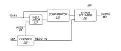
- FIG. 2illustrates an exemplary data compression circuit 200 according to an embodiment of the invention.
- a plurality of the data compression circuit 200may be included in the compression block 120 of FIG. 1 .
- the data compression circuit 200includes a comparator 230 (e.g., a comparison circuit) that receives and compares a first input from a data latch 210 , which latches data received responsive to a previous memory access, and a second input, which includes data received responsive to a most recent memory access.
- a comparator 230e.g., a comparison circuit
- a counter 220provides an active first reset signal RESET # 1 (e.g., the RESET # 1 signal having a high logic value) and an active second reset signal RESET # 2 (e.g., the RESET # 2 signal having a high logic value) to reset the data latch 210 and an error bit latch 240 , respectively.
- the error bit latch 240latches and provides an error bit responsive to an output from the comparator 230 .
- the error bit stored at the error bit latch 240is cleared to a no error detected state responsive to an active RESET # 2 signal.
- the data latch 210receives and latches first data responsive to a first memory access, and the counter 220 changes (e.g., changes or decrements) responsive to a clock signal. Second data is subsequently received responsive to a second memory access and the counter 220 changes based on the clock signal.
- the comparator 230performs a comparison of the first data with the second data.
- the comparisonfor example, may be a bitwise comparison using an XNOR gate.
- the comparator 230provides a result of the comparison having a value that is indicative of whether an error is detected (e.g., a value of the first data is different from a value of the second data). Responsive to the result indicating that an error in the data is detected, the error bit latch 240 sets the error bit to an error detected state and latches the error bit in the error state. Otherwise, the error bit latch 240 maintains the no error detected state. That is, a state of the error bit latched at the error bit latch 240 may remain unchanged responsive to a successful comparison (e.g., a value of first data equals a value of second data).
- the counter 220may provide an active RESET # 1 signal to the data latch 210 to reset the data latch 210 when a value of the counter 220 indicates a second clock signal cycle has completed.
- the data latch 210may receive and latch third data responsive to a third memory access, and the counter 220 may change responsive to the clock signal. Further, fourth data may be received responsive to a fourth memory access, with the counter 220 changing responsive to the clock signal.
- the comparator 230performs a second comparison of the third data with the fourth data, and the error bit latch 240 sets the error bit to the error detected state and latches the error bit having the error detected state based on result data provided by the comparator 230 responsive to the comparison of the third data and the fourth data. If no error is detected based on the comparison, the state of the error bit at the error bit latch remains unchanged from a previous comparison.
- the latching of data, comparison of the data, and changing the state of the error bit from two memory accessesmay continue until a value of the counter 220 is equal to a count of data to be compressed into an error bit. If an error is detected based on any of the comparisons, the error bit having the error detected state remains latched at the error bit latch 240 until reset by the counter 220 .
- the error bitis provided at an output to indicate whether one or more memory cells in a group of memory cells associated with a particular repair address failed the test.
- the counter 220Responsive to the value of the counter being equal to the number of data to be compressed into an error bit, the counter 220 provides an active RESET # 2 signal to the error bit latch 240 to clear (e.g., reset) the error bit to the no error detected state prior to receiving data from a subsequent memory access. In an embodiment, the counter 220 may be reset after providing the active RESET # 2 signal to clear the error bit latch 240 .
- the data compression circuit 200may receive eight data bits, where each bit is received responsive to a respective (e.g., corresponding) memory access of eight total memory accesses.
- the comparator 230may perform a comparison of pairs of the eight received data bits (e.g., for a total of four comparisons).
- the counter 220may reset the data latch 210 after each comparison by providing an active RESET # 1 signal.
- the error bit latch 240may latch an error bit having the error detected state responsive to a result from the comparator 230 having a value indicating the detection of an error.
- the counter 220may clear the error bit to the no error detected value at the error bit latch 240 after the fourth comparison has been performed.
- the error bitmay be cleared responsive to the clock signal by providing an active RESET # 2 signal.
- the compression block 120 of FIG. 1may include 128 of the data compression circuits 200 , one for each of the 128 I/O channels.
- the data compression circuit 200may be modified to latch more than one bit prior to performing a comparison at the comparator 230 , and that the comparator 230 may be modified to compare more than two bits. Further, more or less than 8 bits of data can be compressed into an error bit. In an embodiment, the number of data bits that are compressed may depend on the configuration (e.g., number of columns wide) of the redundancy memory elements for a group.
- the data compression circuit 200compresses each bit corresponding to a respective group into a single error bit, where each bit of the respective group is retrieved responsive to a respective memory access in a plurality of sequential memory accesses. Compression of data received responsive to a memory access, where each bit of the data corresponds to a unique column group would result in an inability to identify failure of a specific group of memory cells associated with a repair address.
- a flow chart of a particular illustrative embodiment of a method of compressing data received responsive to a plurality of memory accessesis designated 300 .
- the method 300may be performed by the apparatus 100 of FIG. 1 and/or the data compression circuit 200 of FIG. 2 .
- the method 300may include receiving and latching first data responsive to a first memory access at a data compression circuit, at step 310 .
- the data compression circuitmay include the data compression block 120 of FIG. 1 and/or the data compression circuit 200 of FIG. 2 .
- the methodmay further include changing (e.g., incrementing or decrementing) a counter, at step 315 .
- the countermay include the counter 220 of FIG. 2 .
- the countermay change responsive to a clock signal.
- the method 300may further include receiving second data responsive to a second memory access at the data compression circuit, at step 320 .
- the methodmay further include changing the counter, at step 325 .
- the methodmay further include comparing the first data and second data, at step 330 .
- the comparisonmay be a bitwise comparison using XNOR logic.
- the method 300further includes determining whether the first data and the second data match based on the comparison, at step 335 . In the method 300 , if the first data does not match the second data, setting an error bit to an error detected state and latching the error bit having the error detected state, at step 340 . If the first data matches the second data, the method 300 further includes maintaining a state of the error bit currently latched in the error bit latch. The method 300 further includes determining whether a value of the counter equal to M, at step 345 . A value of M may be equal to a count of data to be compressed into an error bit.
- the method 300further includes resetting a latch storing the first data, at step 355 , and repeating steps 310 to 345 to compare data responsive to subsequent memory accesses. If the value of the counter is equal to M, the method 300 further includes outputting a value of the error bit, at step 350 . If the value of the counter is equal to M, the method 300 may further include resetting the error bit to a no error detected state at the error bit latch after outputting the error bit.
- an exemplary timing diagram of a particular illustrative embodiment of a data compression responsive to a plurality of memory accessesis disclosed and generally designated 400 .
- the exemplary timing diagram 400may illustrate timing characteristics of the apparatus 100 of FIG. 1 , the compression circuit 200 of FIG. 2 , and/or the method 300 of FIG. 3 .
- the timing diagram 400is exemplary in illustrating the specific, non-limiting example described with reference to FIGS. 1 and 2 , where an array includes 128 I/O channels, and eight bits of data from each channel are compressed into an error bit. Accordingly, 128 column groups are contemporaneously evaluated in 128 compression circuits of a compression block, with each of the 128 column groups configured to provide data to a respective I/O channel.
- the timing diagramcould be modified to, for example, account for a different number of I/O channels, a different count of data bits to compress, or an architecture requiring more or less than two clock cycles per read command.
- the timing diagramincludes a clock signal CLK 410 , a command signal COMMAND 420 , and data input/outputs DQ0-DQ3 430 , 440 , 450 , and 460 .
- a first compression test cycle beginning at time T 0 and ending at time T 1may include issuing a plurality of memory access commands beginning with a first memory access at time T 0 .
- a memory access commandis issued every two CLK signal 410 cycles (e.g., READ ADD 0-7), with a no-operation (NOP) command issued between each memory access.
- NOPno-operation
- each respective compression circuitmay compare data received responsive to eight memory accesses. After eight memory access commands have been issued, the compression block will produce error data including 128 error bits to provide at an output, where each of the 128 error bits is associated with a different column group.
- each error bit of the 128 error bitsmay be generated by a respective compression circuit 200 of FIG.
- the 128 error bitsmay be serially output from a single DQ, such as DQ0 430 , or may be divided amongst two or more DQs (e.g., DQ0-DQ3), with a subset of the error bits serially output from a respective DQ.
- the error bitsare split to be output from DQ0-DQ3 430 , 440 , 450 , and 460 .
- Err bit 0is output, which may be associated with a first column group.
- Subsequent error bits Err bit 1 - 31 provided by DQ0 430may be serially output responsive to the CLK signal 410 .
- DQ1may provide error bits Err bit 32 - 63
- DQ2may provide error bits Err bit 64 - 95
- DQ3may provide error bits Err bit 96 - 127 .
- each compression circuitmay reset an error bit latch storing a respective error bit.
- a second compression test cyclemay begin at time T 1 with issuance of memory access command READ ADD 8, and may conclude after eight memory accesses, e.g., after READ ADD 15 at time T 2 .
- error data including error bits 128 - 255may be output by the compression circuits, with each bit corresponding to a respective column group.
- the memory 500may include a memory array 502 of memory cells, which may be, for example, dynamic random-access memory (DRAM) memory cells, static random-access memory (SRAM) memory cells, flash memory cells, or some other types of memory cells.
- the memory 500includes a command decoder 506 that may receive memory commands through a command bus 508 and generate corresponding control signals within the memory 500 to carry out various memory operations. Row and column address signals may be applied to an address latch 510 in the memory 500 through an address bus 520 . The address latch 510 may then output a separate column address and a separate row address.
- the address latch 510may provide row and column addresses to a row address decoder 522 and a column address decoder 528 , respectively.
- the column address decoder 528may select bit lines extending through the memory array 502 corresponding to respective column addresses.
- the row address decoder 522may be connected to a word line driver 524 that activates respective rows of memory cells in the memory array 502 corresponding to received row addresses.
- the selected data line(e.g., a bit line or bit lines) corresponding to a received column address may be coupled to a read/write circuitry 530 to provide read data to a data output buffer 534 via an input-output (I/O) data bus 540 .
- I/Oinput-output
- Write datamay be applied to the memory array 502 through a data input buffer 544 and the memory array read/write circuitry 530 .
- the command decoder 506may respond to memory commands applied to the command bus 508 to perform various operations on the memory array 502 .
- the command decoder 506may be used to generate internal control signals to read data from and write data to the memory array 502 .
- the compression block 560may include the compression block 120 of FIG. 1 and/or the compression circuit 200 of FIG. 2 , and may be capable of performing the method 300 of FIG. 3 .
- the compression block 560may be configured to perform a data compression of data that is provided responsive to a plurality of memory accesses according to one of the embodiments described above or some other embodiment.
- the compression block 560may be configured to compress data received responsive to the plurality of memory accesses into error data, and provide the error data at an output of the memory 500 .
Landscapes
- Engineering & Computer Science (AREA)
- General Engineering & Computer Science (AREA)
- Physics & Mathematics (AREA)
- General Physics & Mathematics (AREA)
- Theoretical Computer Science (AREA)
- Quality & Reliability (AREA)
- For Increasing The Reliability Of Semiconductor Memories (AREA)
Abstract
Description
- Embodiments of the invention relate generally to electronic memories, and more particularly, in one or more of the illustrated embodiments, to data compression that may be used during testing of electronic memories.
- Advances in technology have resulted in the need for high density memory architecture(s). Memory devices require testing of each individual bit before that memory device can be shipped. As density of memory architectures increase, the time required during testing of these memory devices also increases. Compressing data during testing may be done to improve test efficiency. In current architectures, an access of a memory may retrieve individual bits of data from several individual memory locations that are associated with the address location identified in the access. Those individual bits are pipelined to output drivers to provide the individual bits of data to an external source. A number of input/output (I/O) channels used to provide the individual bits of data to the external source varies based on a type of memory device and architecture of the memory device.
- Existing compression schemes may retrieve the individual bits of data from a single memory access and compress the individual bits together in a manner that reduces a time (e.g., a number of clock cycles) required to test an entire memory array of the memory device and with fewer output pins as compared with a native mode of the memory device. To allow a memory device to repair defective bits identified during testing, individual bits of data that are compressed from the single memory access typically correspond to a common repair address.
- Future architectures may include memory accesses where each individual bit of data retrieved responsive to a memory access may correspond to a different repair address. Traditional compression methods compressing individual bits of a single memory access are ineffective in architectures where the individual bits of data correspond to different repair addresses, as compression would result in an inability to identify a repair address associated with a defective bit. Testing without using compression may be inefficient and may result in a substantial increase in test time.
FIG. 1 is a block diagram of a particular illustrative embodiment of an apparatus including a data compression block;FIG. 2 is a block diagram of a particular illustrative embodiment of a data compression circuit;FIG. 3 is a flow chart of a particular illustrative embodiment of a method of compressing received responsive to a plurality of memory accesses;FIG. 4 is an exemplary timing diagram of a particular illustrative embodiment of a data compression responsive to a plurality of memory accesses; andFIG. 5 is a block diagram of a memory including a data compression circuit according to an embodiment of the invention.- Certain details are set forth below to provide a sufficient understanding of embodiments of the invention. However, it will be clear to one having skill in the art that embodiments of the invention may be practiced without these particular details. Moreover, the particular embodiments of the present invention described herein are provided by way of example and should not be used to limit the scope of the invention to these particular embodiments.
- Referring to
FIG. 1 , a particular illustrative embodiment of an apparatus (e.g., an integrated circuit, a memory device, a memory system, an electronic device or system, a smart phone, a tablet, a computer, a server, etc.) including a data compression block is disclosed and generally designated100. Theapparatus 100 may facilitate data compression during memory testing in architectures where data is read from groups of memory cells of an array, and each group of memory cells is associated with a respective (e.g., different) repair address. Each group of memory cells may provide respective binary digit or digits (e.g., “bit” or “bits”) of the data read responsive to a memory access command. That data read may be test data previously written for testing of the memory. The data is compressed by compressing corresponding bits of the data read responsive to a plurality of independent memory access commands. For example, a bit at the least significant bit (LSB) position of first data read responsive to a first memory access command is compressed with a bit also in the same LSB position of second data read responsive to a second memory access command. Likewise, a bit at the most significant bit (MSB) position of the first data is compressed with a bit also in the same MSB position of the second data. In another embodiment, portions of data retrieved from a group of memory cells corresponding to a particular repair address received over a plurality of memory accesses may be included at different positions of two or more of the plurality of memory accesses. - The
apparatus 100 may include amemory array 110 that includes X+1 memory array regions, such as memory array regions 0-X112(0)-(X). Each of the memory array regions 0-X112(0)-(X) may include respective plurality of groups of memory cells from which data is read responsive to a memory access command. Thememory array 110 may be coupled to acompression block 120. Thecompression block 120 may compress data received responsive to a plurality of memory accesses to produce error data. - As explained above, the
memory array 110 may include X+1 memory array regions 0-X112(0)-(X). Each memory array region may include memory cells arranged in an array having a plurality of rows and a plurality of columns. The plurality of columns may be divided into column groups, and in some embodiments, each column group is associated with a respective I/O channel of a plurality of I/O channels. For example, a first column group may be associated with a first I/O channel, a second column group may be associated with a second I/O channel, etc. A respective bit of the data may be read from a column group responsive to a memory access command. In another embodiment, the plurality of rows may be divided into row groups, and, each row group may be associated with a respective I/O channel of a plurality of I/O channels. For example, a respective bit of the data may be read from a row group responsive to a memory access command. - Each of the memory array regions 0-X112(0)-(X) may be associated with respective sets of redundancy memory elements that are used to repair defective memory cells by mapping defective cells to a redundancy memory element. A redundancy memory element may replace a plurality of adjacent memory cells, for example, a plurality of memory cells along a row or rows, a plurality of memory cells along a column or columns, or a plurality of memory cells within an array of rows and columns. That is, in using a redundancy memory element to repair a defective memory cell or defective memory cells, the redundancy memory element will in effect replace not only the defective memory cell or defective memory cells, but all of the memory cells of the plurality of adjacent memory cells covered by the redundancy memory element. The number of memory cells of the plurality of adjacent memory cells replaced by a redundancy memory element, and the arrangement of the memory cells of the plurality of adjacent memory cells may be based on an architecture of the
memory array 110. - In some embodiments, each column group may be associated with a respective set of redundancy memory elements that may be used for repairing defective memory cells within the column group. Thus, a defective memory cell or defective memory cells of a column group may be replaced with a redundancy memory element of the respective set of redundancy memory elements associated with that column group. In another embodiment, each row group may be associated with a respective set of redundancy memory elements that may be used for repairing defective memory cells within the respective row group.
- The
compression block 120 may include a plurality of data compression circuits. An embodiment of a data compression circuit that may be used will be described below in greater detail with reference toFIG. 2 . Thecompression block 120 may receive data read responsive to a plurality of memory accesses from the column groups of a memory array region of thememory array 110. Each of the column groups may provide a respective bit of the data read for each memory access. Thecompression block 120 may then compress the data read from the respective column groups using comparison logic to provide error data that indicates whether the respective column groups have a defective memory cell or memory cells. The error data provided by the data compression circuits may be stored in a buffer in thecompression block 120 to be later provided. - During operation, data are each retrieved from a particular region (e.g., one of the memory array regions 0-X112(0)-(X) of the memory array110) responsive to a memory access. The data written to a particular region of the
memory array 110 may be test data. Each bit of the data may be read from a respective column group, and each of the column groups may be associated with a respective repair address that is distinct from repair addresses associated with the other column groups that provided bits of the memory access data. For example, a first bit of the data may be read from a first column group associated with a first repair address, a second bit of the data may be read from a second column group associated with a second repair address, etc. Further, each bit position of each of the plurality of data may be associated with a respective column group. - Each bit of the data may be provided to the
compression block 120 from a column group via an associated I/O channel. For example, a first bit of the data is provided to a first data compression circuit of thecompression block 120 via a first I/O channel, a second bit of the data is provided to a second data compression circuit of thecompression block 120 via a second I/O channel, etc. Thus, with each memory access, each I/O channel will provide a respective bit of data from a respective column group associated with a respective repair address. In some embodiments, each I/O channel may provide more than one bit to thecompression block 120. For example, a first subset of bits of the data is provided to thecompression block 120 via a first I/O channel, a second subset of bits of the data is provided to thecompression block 120 via a second I/O channel, etc. In other embodiments, if, for example, a first bit of the data and a second bit of the data correspond to a common repair address, the first bit of the data is provided to the first data compression circuit of thecompression block 120 via the first I/O channel and the second bit of the data is provided to the first data compression circuit of thecompression block 120 via the second I/O channel. - As previously discussed, the
compression block 120 may include a plurality of data compression circuits (not shown inFIG. 1 ). In some embodiments, thecompression block 120 includes a respective data compression circuit for each of the I/O channels. In another embodiment, thecompression block 120 includes a respective data compression circuit for each of one or more subsets of bits of a memory access to be compressed. For example, if a memory access provides 128 bits of data, and 64 of bits of the data are from different repair addresses, and a remaining 64 bits are from a common repair address, the compression block may require at least 65 data compression circuits. Alternatively, if the data includes 4 bits of data from each of 32 unique repair addresses, the compression block may require at least 32 data compression circuits. An example of a data compression circuit of thecompression block 120 is described in further detail with reference toFIG. 2 . In some embodiments, a data compression circuit compares the data received via a respective I/O channel responsive to each of the plurality of memory accesses. In another embodiment, a data compression circuit may compare data corresponding to a particular repair address that is received via two or more respective I/O channels responsive to each of the plurality of memory accesses. Prior to comparison of the data provided on the respective I/O channel, an error bit is cleared to a no error detected state at the data compression circuit. Responsive to detection of an error in the data provided on a respective I/O channel based on the comparison (e.g., the data is mismatched), the error bit may be set to an error detected state at the data compression circuit, and the error bit having the error detected state is latched in the data compression circuit, for example, by an error bit latch. If no error is detected in the data provided on the respective I/O channel based on the comparison, the error bit remains in the no error detected state at the error bit latch. By comparing the data provided on a respective I/O channel and clearing and/or setting a state of the error bit based on the comparison, the data read from a column group may be compressed into the error bit having a state that indicates whether any of the memory cells read from the respective column group are defective. That is, a state of the error bit latched may remain unchanged responsive to a successful comparison (e.g., data is not mismatched) and changed to the error detected state responsive to an unsuccessful comparison. Thus, if the error bit has the no error detected state responsive to completion of the comparison of the data, then no errors were detected in the data. If the error bit has the error detected state responsive to completion of the comparison of the data, then at least one error was detected in at least one bit of the data. As a result, each data compression circuit may compress data from a respective column group that is associated with a common repair address. Error data, which may include each of the error bits, may be stored in a buffer (not shown) and then provided at an output of thecompression block 120. Responsive to completion of compressing error data for one or more column groups, the error data may be serially output from an output buffer (not shown) of the apparatus via one or more outputs DQs (not shown). The error data may be output contemporaneously with compression of data from additional column groups of thememory array 110. - In a specific, non-limiting example, each region of the
memory array 110 includes 128 column groups, each column group associated with a respective I/O channel. A memory access may retrieve 128 bits, one bit from each column group via a respective I/O channel. Additionally, each of the 128 bits are associated with a different repair address by virtue of being read from a respective column group. Thecompression block 120 may include 128 data compression circuits to process data read from 128 column groups and associated with 128 different repair addresses. Further in the non-limiting example, each data compression circuit compresses eight bits from a respective column group. Accordingly, eight memory accesses are used to read eight bits from the respective column group. Each of the eight bits may be read from a different memory cell of the column group. In some embodiments, each of the eight different memory cells is coupled to a respective column of memory. The eight bits of data are compressed by a data compression circuit to one corresponding error bit. Thus, over the course of the eight memory accesses, eight bits from each of 128 column group, or 1024 total bits, are compressed into 128 error bits, which are included in the error data output from thecompression block 120. Thus, in this example, four DQ, 128 clock cycles would be required to output the data without compression and 16 would be required to output the data with compression. - The preceding example is not intended to limit embodiments of the invention to the particular details previously discussed. Those of skill in the art would appreciate that the invention should not be limited as such. Further, one of ordinary skill in the art would recognize that a set of redundancy memory elements may be associated with a respective group of memory cells other than a column group(s) or a row group(s). For example, a set of redundancy memory elements may be associated with a group of memory cells that corresponds to a subset of columns of the plurality of columns and a subset of rows of the plurality of rows.
FIG. 2 illustrates an exemplarydata compression circuit 200 according to an embodiment of the invention. A plurality of thedata compression circuit 200 may be included in thecompression block 120 ofFIG. 1 . Thedata compression circuit 200 includes a comparator230 (e.g., a comparison circuit) that receives and compares a first input from adata latch 210, which latches data received responsive to a previous memory access, and a second input, which includes data received responsive to a most recent memory access. Acounter 220 provides an active first reset signal RESET #1 (e.g., theRESET # 1 signal having a high logic value) and an active second reset signal RESET #2 (e.g., theRESET # 2 signal having a high logic value) to reset the data latch210 and anerror bit latch 240, respectively. Theerror bit latch 240 latches and provides an error bit responsive to an output from thecomparator 230.- In operation, prior to an initial comparison, the error bit stored at the
error bit latch 240 is cleared to a no error detected state responsive to anactive RESET # 2 signal. The data latch210 receives and latches first data responsive to a first memory access, and thecounter 220 changes (e.g., changes or decrements) responsive to a clock signal. Second data is subsequently received responsive to a second memory access and thecounter 220 changes based on the clock signal. Thecomparator 230 performs a comparison of the first data with the second data. The comparison, for example, may be a bitwise comparison using an XNOR gate. Thecomparator 230 provides a result of the comparison having a value that is indicative of whether an error is detected (e.g., a value of the first data is different from a value of the second data). Responsive to the result indicating that an error in the data is detected, theerror bit latch 240 sets the error bit to an error detected state and latches the error bit in the error state. Otherwise, theerror bit latch 240 maintains the no error detected state. That is, a state of the error bit latched at theerror bit latch 240 may remain unchanged responsive to a successful comparison (e.g., a value of first data equals a value of second data). Thecounter 220 may provide anactive RESET # 1 signal to the data latch210 to reset the data latch210 when a value of thecounter 220 indicates a second clock signal cycle has completed. - Subsequently, the data latch210 may receive and latch third data responsive to a third memory access, and the
counter 220 may change responsive to the clock signal. Further, fourth data may be received responsive to a fourth memory access, with thecounter 220 changing responsive to the clock signal. Thecomparator 230 performs a second comparison of the third data with the fourth data, and theerror bit latch 240 sets the error bit to the error detected state and latches the error bit having the error detected state based on result data provided by thecomparator 230 responsive to the comparison of the third data and the fourth data. If no error is detected based on the comparison, the state of the error bit at the error bit latch remains unchanged from a previous comparison. The latching of data, comparison of the data, and changing the state of the error bit from two memory accesses may continue until a value of thecounter 220 is equal to a count of data to be compressed into an error bit. If an error is detected based on any of the comparisons, the error bit having the error detected state remains latched at theerror bit latch 240 until reset by thecounter 220. The error bit is provided at an output to indicate whether one or more memory cells in a group of memory cells associated with a particular repair address failed the test. Responsive to the value of the counter being equal to the number of data to be compressed into an error bit, thecounter 220 provides anactive RESET # 2 signal to theerror bit latch 240 to clear (e.g., reset) the error bit to the no error detected state prior to receiving data from a subsequent memory access. In an embodiment, thecounter 220 may be reset after providing theactive RESET # 2 signal to clear theerror bit latch 240. - In the specific, non-limiting example described with reference to
FIG. 1 , thedata compression circuit 200 may receive eight data bits, where each bit is received responsive to a respective (e.g., corresponding) memory access of eight total memory accesses. Thecomparator 230 may perform a comparison of pairs of the eight received data bits (e.g., for a total of four comparisons). Thecounter 220 may reset the data latch210 after each comparison by providing anactive RESET # 1 signal. Theerror bit latch 240 may latch an error bit having the error detected state responsive to a result from thecomparator 230 having a value indicating the detection of an error. Thecounter 220 may clear the error bit to the no error detected value at theerror bit latch 240 after the fourth comparison has been performed. The error bit may be cleared responsive to the clock signal by providing anactive RESET # 2 signal. Further related to the specific non-limiting example described with reference toFIG. 1 , thecompression block 120 ofFIG. 1 may include 128 of thedata compression circuits 200, one for each of the 128 I/O channels. - The
data compression circuit 200 may be modified to latch more than one bit prior to performing a comparison at thecomparator 230, and that thecomparator 230 may be modified to compare more than two bits. Further, more or less than 8 bits of data can be compressed into an error bit. In an embodiment, the number of data bits that are compressed may depend on the configuration (e.g., number of columns wide) of the redundancy memory elements for a group. - The
data compression circuit 200 compresses each bit corresponding to a respective group into a single error bit, where each bit of the respective group is retrieved responsive to a respective memory access in a plurality of sequential memory accesses. Compression of data received responsive to a memory access, where each bit of the data corresponds to a unique column group would result in an inability to identify failure of a specific group of memory cells associated with a repair address. - Referring to
FIG. 3 , a flow chart of a particular illustrative embodiment of a method of compressing data received responsive to a plurality of memory accesses is designated300. Themethod 300 may be performed by theapparatus 100 ofFIG. 1 and/or thedata compression circuit 200 ofFIG. 2 . - The
method 300 may include receiving and latching first data responsive to a first memory access at a data compression circuit, atstep 310. The data compression circuit may include thedata compression block 120 ofFIG. 1 and/or thedata compression circuit 200 ofFIG. 2 . The method may further include changing (e.g., incrementing or decrementing) a counter, atstep 315. The counter may include thecounter 220 ofFIG. 2 . The counter may change responsive to a clock signal. - The
method 300 may further include receiving second data responsive to a second memory access at the data compression circuit, atstep 320. The method may further include changing the counter, atstep 325. The method may further include comparing the first data and second data, atstep 330. The comparison may be a bitwise comparison using XNOR logic. - The
method 300 further includes determining whether the first data and the second data match based on the comparison, atstep 335. In themethod 300, if the first data does not match the second data, setting an error bit to an error detected state and latching the error bit having the error detected state, atstep 340. If the first data matches the second data, themethod 300 further includes maintaining a state of the error bit currently latched in the error bit latch. Themethod 300 further includes determining whether a value of the counter equal to M, atstep 345. A value of M may be equal to a count of data to be compressed into an error bit. - If the value of the counter is not equal to M, the
method 300 further includes resetting a latch storing the first data, atstep 355, and repeatingsteps 310 to345 to compare data responsive to subsequent memory accesses. If the value of the counter is equal to M, themethod 300 further includes outputting a value of the error bit, atstep 350. If the value of the counter is equal to M, themethod 300 may further include resetting the error bit to a no error detected state at the error bit latch after outputting the error bit. - Referring to
FIG. 4 , an exemplary timing diagram of a particular illustrative embodiment of a data compression responsive to a plurality of memory accesses is disclosed and generally designated400. For example, the exemplary timing diagram400 may illustrate timing characteristics of theapparatus 100 ofFIG. 1 , thecompression circuit 200 ofFIG. 2 , and/or themethod 300 ofFIG. 3 . The timing diagram400 is exemplary in illustrating the specific, non-limiting example described with reference toFIGS. 1 and 2 , where an array includes 128 I/O channels, and eight bits of data from each channel are compressed into an error bit. Accordingly, 128 column groups are contemporaneously evaluated in 128 compression circuits of a compression block, with each of the 128 column groups configured to provide data to a respective I/O channel. The timing diagram could be modified to, for example, account for a different number of I/O channels, a different count of data bits to compress, or an architecture requiring more or less than two clock cycles per read command. The timing diagram includes aclock signal CLK 410, acommand signal COMMAND 420, and data input/outputs DQ0-DQ3 - A first compression test cycle beginning at time T0 and ending at time T1, may include issuing a plurality of memory access commands beginning with a first memory access at time T0. A memory access command is issued every two CLK signal410 cycles (e.g., READ ADD 0-7), with a no-operation (NOP) command issued between each memory access. In an embodiment where eight data bits are provided for each repair address, each respective compression circuit may compare data received responsive to eight memory accesses. After eight memory access commands have been issued, the compression block will produce error data including 128 error bits to provide at an output, where each of the 128 error bits is associated with a different column group. In an example, each error bit of the 128 error bits may be generated by a
respective compression circuit 200 ofFIG. 2 . The 128 error bits may be serially output from a single DQ, such asDQ0 430, or may be divided amongst two or more DQs (e.g., DQ0-DQ3), with a subset of the error bits serially output from a respective DQ. In the exemplary embodiment of the timing diagram400, the error bits are split to be output from DQ0-DQ3 Err bit 0 is output, which may be associated with a first column group. Subsequent error bits Err bit1-31 provided byDQ0 430 may be serially output responsive to theCLK signal 410. Similarly, beginning at time T1, DQ1 may provide error bits Err bit32-63, DQ2 may provide error bits Err bit64-95, and DQ3 may provide error bits Err bit96-127. - Additionally, at time T1, after each compression circuit has provided a respective error bit, each compression circuit may reset an error bit latch storing a respective error bit. A second compression test cycle may begin at time T1 with issuance of memory access
command READ ADD 8, and may conclude after eight memory accesses, e.g., afterREAD ADD 15 at time T2. At an end of the second compression test cycle, Time T2, error data including error bits128-255 may be output by the compression circuits, with each bit corresponding to a respective column group. - Referring to
FIG. 5 , a block diagram of amemory 500 including acompression block 560 according to an embodiment of the invention is disclosed. Thememory 500 may include amemory array 502 of memory cells, which may be, for example, dynamic random-access memory (DRAM) memory cells, static random-access memory (SRAM) memory cells, flash memory cells, or some other types of memory cells. Thememory 500 includes acommand decoder 506 that may receive memory commands through acommand bus 508 and generate corresponding control signals within thememory 500 to carry out various memory operations. Row and column address signals may be applied to anaddress latch 510 in thememory 500 through anaddress bus 520. Theaddress latch 510 may then output a separate column address and a separate row address. - The
address latch 510 may provide row and column addresses to arow address decoder 522 and acolumn address decoder 528, respectively. Thecolumn address decoder 528 may select bit lines extending through thememory array 502 corresponding to respective column addresses. Therow address decoder 522 may be connected to aword line driver 524 that activates respective rows of memory cells in thememory array 502 corresponding to received row addresses. The selected data line (e.g., a bit line or bit lines) corresponding to a received column address may be coupled to a read/write circuitry 530 to provide read data to adata output buffer 534 via an input-output (I/O)data bus 540. Write data may be applied to thememory array 502 through adata input buffer 544 and the memory array read/write circuitry 530. Thecommand decoder 506 may respond to memory commands applied to thecommand bus 508 to perform various operations on thememory array 502. In particular, thecommand decoder 506 may be used to generate internal control signals to read data from and write data to thememory array 502. - The
compression block 560 may include thecompression block 120 ofFIG. 1 and/or thecompression circuit 200 ofFIG. 2 , and may be capable of performing themethod 300 ofFIG. 3 . For example, thecompression block 560 may be configured to perform a data compression of data that is provided responsive to a plurality of memory accesses according to one of the embodiments described above or some other embodiment. Thecompression block 560 may be configured to compress data received responsive to the plurality of memory accesses into error data, and provide the error data at an output of thememory 500. - Those of ordinary skill would further appreciate that the various illustrative logical blocks, configurations, modules, circuits, and algorithm steps described in connection with the embodiments disclosed herein may be implemented as electronic hardware, computer software executed by a processor, or combinations of both. Various illustrative components, blocks, configurations, modules, circuits, and steps have been described above generally in terms of their functionality. Whether such functionality is implemented as hardware or processor executable instructions depends upon the particular application and design constraints imposed on the overall system. Skilled artisans may implement the described functionality in varying ways for each particular application, but such implementation decisions should not be interpreted as causing a departure from the scope of the present disclosure.
- The previous description of the disclosed embodiments is provided to enable a person skilled in the art to make or use the disclosed embodiments. Various modifications to these embodiments will be readily apparent to those skilled in the art, and the principles defined herein may be applied to other embodiments without departing from the scope of the disclosure. Thus, the present disclosure is not intended to be limited to the embodiments shown herein but is to be accorded the widest scope possible consistent with the principles and novel features as defined by the following claims.
Claims (27)
Priority Applications (1)
| Application Number | Priority Date | Filing Date | Title |
|---|---|---|---|
| US13/771,838US9183952B2 (en) | 2013-02-20 | 2013-02-20 | Apparatuses and methods for compressing data received over multiple memory accesses |
Applications Claiming Priority (1)
| Application Number | Priority Date | Filing Date | Title |
|---|---|---|---|
| US13/771,838US9183952B2 (en) | 2013-02-20 | 2013-02-20 | Apparatuses and methods for compressing data received over multiple memory accesses |
Publications (2)
| Publication Number | Publication Date |
|---|---|
| US20140237305A1true US20140237305A1 (en) | 2014-08-21 |
| US9183952B2 US9183952B2 (en) | 2015-11-10 |
Family
ID=51352197
Family Applications (1)
| Application Number | Title | Priority Date | Filing Date |
|---|---|---|---|
| US13/771,838Active2033-07-26US9183952B2 (en) | 2013-02-20 | 2013-02-20 | Apparatuses and methods for compressing data received over multiple memory accesses |
Country Status (1)
| Country | Link |
|---|---|
| US (1) | US9183952B2 (en) |
Cited By (5)
| Publication number | Priority date | Publication date | Assignee | Title |
|---|---|---|---|---|
| CN105448334A (en)* | 2014-09-01 | 2016-03-30 | 华邦电子股份有限公司 | Semiconductor storage apparatus |
| US9817738B2 (en)* | 2015-09-04 | 2017-11-14 | Intel Corporation | Clearing poison status on read accesses to volatile memory regions allocated in non-volatile memory |
| CN110214348A (en)* | 2017-01-31 | 2019-09-06 | 辛纳普蒂克斯公司 | Apparatus and method for driving a display panel in response to image data |
| CN111989580A (en)* | 2019-01-22 | 2020-11-24 | 爱德万测试公司 | Automated test equipment for testing one or more devices under test, method for automated testing of one or more devices under test and computer program for handling command errors |
| US20240103951A1 (en)* | 2021-12-21 | 2024-03-28 | Nvidia Corporation | Error rate interrupts in hardware for high-speed signaling interconnect |
Citations (28)
| Publication number | Priority date | Publication date | Assignee | Title |
|---|---|---|---|---|
| US5535164A (en)* | 1995-03-03 | 1996-07-09 | International Business Machines Corporation | BIST tester for multiple memories |
| US5805789A (en)* | 1995-12-14 | 1998-09-08 | International Business Machines Corporation | Programmable computer system element with built-in self test method and apparatus for repair during power-on |
| US5859804A (en)* | 1991-10-16 | 1999-01-12 | International Business Machines Corporation | Method and apparatus for real time two dimensional redundancy allocation |
| US5913928A (en)* | 1997-05-09 | 1999-06-22 | Micron Technology, Inc. | Data compression test mode independent of redundancy |
| US5935263A (en)* | 1997-07-01 | 1999-08-10 | Micron Technology, Inc. | Method and apparatus for memory array compressed data testing |
| US6065134A (en)* | 1996-02-07 | 2000-05-16 | Lsi Logic Corporation | Method for repairing an ASIC memory with redundancy row and input/output lines |
| US6069829A (en)* | 1998-09-29 | 2000-05-30 | Texas Instruments Incorporated | Internal clock multiplication for test time reduction |
| US6072737A (en)* | 1998-08-06 | 2000-06-06 | Micron Technology, Inc. | Method and apparatus for testing embedded DRAM |
| US6081910A (en)* | 1993-06-30 | 2000-06-27 | International Business Machines Corporation | Circuit for allowing a two-pass fuse blow to memory chips combining an array built-in self-test with redundancy capabilities |
| US6138254A (en)* | 1998-01-22 | 2000-10-24 | Micron Technology, Inc. | Method and apparatus for redundant location addressing using data compression |
| US6269455B1 (en)* | 1996-11-07 | 2001-07-31 | Acuid Corporation Limited | System and a method for processing information about locations of defective memory cells and a memory test with defect compression means |
| US20020157051A1 (en)* | 2001-04-24 | 2002-10-24 | International Business Machines Corporation | Method and apparatus for ABIST diagnostics |
| US20030088815A1 (en)* | 2001-11-05 | 2003-05-08 | Thomas Boehler | Using data compression for faster testing of embedded memory |
| US6788595B2 (en)* | 2002-08-05 | 2004-09-07 | Silicon Storage Technology, Inc. | Embedded recall apparatus and method in nonvolatile memory |
| US20040181724A1 (en)* | 2000-08-30 | 2004-09-16 | Mcbride Jerry D. | System for storing device test information on a semiconductor device using on-device logic for determination of test results |
| US20040246337A1 (en)* | 2003-03-26 | 2004-12-09 | Kabushiki Kaisha Toshiba | Self-test executable integrated circuit, a design apparatus thereof, and a scan chain design apparatus |
| US6839277B2 (en)* | 2002-09-17 | 2005-01-04 | Silicon Storage Technology, Inc. | User identification for multi-purpose flash memory |
| US20050047229A1 (en)* | 2002-12-18 | 2005-03-03 | Benoit Nadeau-Dostie | Method and circuit for collecting memory failure information |
| US20050066226A1 (en)* | 2003-09-23 | 2005-03-24 | Adams R. Dean | Redundant memory self-test |
| US6920525B2 (en)* | 2002-07-19 | 2005-07-19 | International Business Machines Corporation | Method and apparatus of local word-line redundancy in CAM |
| US20060136792A1 (en)* | 2004-12-16 | 2006-06-22 | Wolfgang Hokenmaier | Random access memory having test circuit |
| US7103815B2 (en)* | 2001-09-28 | 2006-09-05 | Inapac Technology, Inc. | Testing of integrated circuit devices |
| US20070226553A1 (en)* | 2006-03-21 | 2007-09-27 | Khaled Fekih-Romdhane | Multiple banks read and data compression for back end test |
| US7487420B2 (en)* | 2005-02-15 | 2009-02-03 | Cadence Design Systems Inc. | System and method for performing logic failure diagnosis using multiple input signature register output streams |
| US20090158087A1 (en)* | 2007-12-12 | 2009-06-18 | Renesas Technology Corp | Semiconductor integrated circuit with memory repair circuit |
| US20090225610A1 (en)* | 2008-03-05 | 2009-09-10 | Wolfgang Hokenmaier | Integrated circuit that selectively outputs subsets of a group of data bits |
| US7657802B2 (en)* | 2003-01-31 | 2010-02-02 | Micron Technology, Inc. | Data compression read mode for memory testing |
| US20120275247A1 (en)* | 2011-04-28 | 2012-11-01 | Hynix Semiconductor Inc. | Semiconductor memory device and method for repairing the same |
Family Cites Families (2)
| Publication number | Priority date | Publication date | Assignee | Title |
|---|---|---|---|---|
| KR101411499B1 (en) | 2008-05-19 | 2014-07-01 | 삼성전자주식회사 | Variable resistance memory device and management method thereof |
| KR101212737B1 (en) | 2010-12-17 | 2012-12-14 | 에스케이하이닉스 주식회사 | Semiconductor memory device |
- 2013
- 2013-02-20USUS13/771,838patent/US9183952B2/enactiveActive
Patent Citations (34)
| Publication number | Priority date | Publication date | Assignee | Title |
|---|---|---|---|---|
| US6026505A (en)* | 1991-10-16 | 2000-02-15 | International Business Machines Corporation | Method and apparatus for real time two dimensional redundancy allocation |
| US5859804A (en)* | 1991-10-16 | 1999-01-12 | International Business Machines Corporation | Method and apparatus for real time two dimensional redundancy allocation |
| US6081910A (en)* | 1993-06-30 | 2000-06-27 | International Business Machines Corporation | Circuit for allowing a two-pass fuse blow to memory chips combining an array built-in self-test with redundancy capabilities |
| US5535164A (en)* | 1995-03-03 | 1996-07-09 | International Business Machines Corporation | BIST tester for multiple memories |
| US5805789A (en)* | 1995-12-14 | 1998-09-08 | International Business Machines Corporation | Programmable computer system element with built-in self test method and apparatus for repair during power-on |
| US6065134A (en)* | 1996-02-07 | 2000-05-16 | Lsi Logic Corporation | Method for repairing an ASIC memory with redundancy row and input/output lines |
| US6269455B1 (en)* | 1996-11-07 | 2001-07-31 | Acuid Corporation Limited | System and a method for processing information about locations of defective memory cells and a memory test with defect compression means |
| US5913928A (en)* | 1997-05-09 | 1999-06-22 | Micron Technology, Inc. | Data compression test mode independent of redundancy |
| US5935263A (en)* | 1997-07-01 | 1999-08-10 | Micron Technology, Inc. | Method and apparatus for memory array compressed data testing |
| US6138254A (en)* | 1998-01-22 | 2000-10-24 | Micron Technology, Inc. | Method and apparatus for redundant location addressing using data compression |
| US6484278B1 (en)* | 1998-08-06 | 2002-11-19 | Micron Technology, Inc. | Method and apparatus for testing an embedded DRAM |
| US6072737A (en)* | 1998-08-06 | 2000-06-06 | Micron Technology, Inc. | Method and apparatus for testing embedded DRAM |
| US6069829A (en)* | 1998-09-29 | 2000-05-30 | Texas Instruments Incorporated | Internal clock multiplication for test time reduction |
| US20040181724A1 (en)* | 2000-08-30 | 2004-09-16 | Mcbride Jerry D. | System for storing device test information on a semiconductor device using on-device logic for determination of test results |
| US20060156136A1 (en)* | 2000-08-30 | 2006-07-13 | Mcbride Jerry D | System for storing device test information on a semiconductor device using on-device logic for determination of test results |
| US7194667B2 (en)* | 2000-08-30 | 2007-03-20 | Micron Technology, Inc. | System for storing device test information on a semiconductor device using on-device logic for determination of test results |
| US20020157051A1 (en)* | 2001-04-24 | 2002-10-24 | International Business Machines Corporation | Method and apparatus for ABIST diagnostics |
| US7103815B2 (en)* | 2001-09-28 | 2006-09-05 | Inapac Technology, Inc. | Testing of integrated circuit devices |
| US20030088815A1 (en)* | 2001-11-05 | 2003-05-08 | Thomas Boehler | Using data compression for faster testing of embedded memory |
| US6950971B2 (en)* | 2001-11-05 | 2005-09-27 | Infineon Technologies Ag | Using data compression for faster testing of embedded memory |
| US6920525B2 (en)* | 2002-07-19 | 2005-07-19 | International Business Machines Corporation | Method and apparatus of local word-line redundancy in CAM |
| US6788595B2 (en)* | 2002-08-05 | 2004-09-07 | Silicon Storage Technology, Inc. | Embedded recall apparatus and method in nonvolatile memory |
| US6839277B2 (en)* | 2002-09-17 | 2005-01-04 | Silicon Storage Technology, Inc. | User identification for multi-purpose flash memory |
| US20050047229A1 (en)* | 2002-12-18 | 2005-03-03 | Benoit Nadeau-Dostie | Method and circuit for collecting memory failure information |
| US7657802B2 (en)* | 2003-01-31 | 2010-02-02 | Micron Technology, Inc. | Data compression read mode for memory testing |
| US20040246337A1 (en)* | 2003-03-26 | 2004-12-09 | Kabushiki Kaisha Toshiba | Self-test executable integrated circuit, a design apparatus thereof, and a scan chain design apparatus |
| US20050066226A1 (en)* | 2003-09-23 | 2005-03-24 | Adams R. Dean | Redundant memory self-test |
| US20060136792A1 (en)* | 2004-12-16 | 2006-06-22 | Wolfgang Hokenmaier | Random access memory having test circuit |
| US7263638B2 (en)* | 2004-12-16 | 2007-08-28 | Infineon Technologies Ag | Memory having test circuit |
| US7487420B2 (en)* | 2005-02-15 | 2009-02-03 | Cadence Design Systems Inc. | System and method for performing logic failure diagnosis using multiple input signature register output streams |
| US20070226553A1 (en)* | 2006-03-21 | 2007-09-27 | Khaled Fekih-Romdhane | Multiple banks read and data compression for back end test |
| US20090158087A1 (en)* | 2007-12-12 | 2009-06-18 | Renesas Technology Corp | Semiconductor integrated circuit with memory repair circuit |
| US20090225610A1 (en)* | 2008-03-05 | 2009-09-10 | Wolfgang Hokenmaier | Integrated circuit that selectively outputs subsets of a group of data bits |
| US20120275247A1 (en)* | 2011-04-28 | 2012-11-01 | Hynix Semiconductor Inc. | Semiconductor memory device and method for repairing the same |
Non-Patent Citations (1)
| Title |
|---|
| Chen et al., Enabling Embedded Memory Diagnosis via Test Response Compression, 2001, IEEE, pp. 292-298.* |
Cited By (7)
| Publication number | Priority date | Publication date | Assignee | Title |
|---|---|---|---|---|
| CN105448334A (en)* | 2014-09-01 | 2016-03-30 | 华邦电子股份有限公司 | Semiconductor storage apparatus |
| US9817738B2 (en)* | 2015-09-04 | 2017-11-14 | Intel Corporation | Clearing poison status on read accesses to volatile memory regions allocated in non-volatile memory |
| CN110214348A (en)* | 2017-01-31 | 2019-09-06 | 辛纳普蒂克斯公司 | Apparatus and method for driving a display panel in response to image data |
| CN111989580A (en)* | 2019-01-22 | 2020-11-24 | 爱德万测试公司 | Automated test equipment for testing one or more devices under test, method for automated testing of one or more devices under test and computer program for handling command errors |
| US11913990B2 (en) | 2019-01-22 | 2024-02-27 | Advantest Corporation | Automated test equipment for testing one or more devices under test, method for automated testing of one or more devices under test, and computer program for handling command errors |
| US20240103951A1 (en)* | 2021-12-21 | 2024-03-28 | Nvidia Corporation | Error rate interrupts in hardware for high-speed signaling interconnect |
| US12353271B2 (en)* | 2021-12-21 | 2025-07-08 | Nvidia Corporation | Error rate interrupts in hardware for high-speed signaling interconnect |
Also Published As
| Publication number | Publication date |
|---|---|
| US9183952B2 (en) | 2015-11-10 |
Similar Documents
| Publication | Publication Date | Title |
|---|---|---|
| US10445177B2 (en) | Controller-based memory scrub for DRAMs with internal error-correcting code (ECC) bits contemporaneously during auto refresh or by using masked write commands | |
| US9823964B2 (en) | Method for memory scrub of DRAM with internal error correcting code (ECC) bits during either memory activate and/or precharge operation | |
| KR101750662B1 (en) | Circuits, apparatuses, and methods for correcting data errors | |
| US9727412B2 (en) | Memory device having error notification function | |
| US10614906B2 (en) | Semiconductor memory devices, memory systems and methods of operating semiconductor memory devices | |
| US9405721B2 (en) | Apparatuses and methods for performing a databus inversion operation | |
| US7506226B2 (en) | System and method for more efficiently using error correction codes to facilitate memory device testing | |
| US9880900B2 (en) | Method for scrubbing and correcting DRAM memory data with internal error-correcting code (ECC) bits contemporaneously during self-refresh state | |
| US10908990B2 (en) | Shared address counters for multiple modes of operation in a memory device | |
| US9923578B2 (en) | Parity check circuit and memory device including the same | |
| US9183952B2 (en) | Apparatuses and methods for compressing data received over multiple memory accesses | |
| CN110942798B (en) | Semiconductor memory device, memory system, and method for operating a semiconductor memory device | |
| US20070097760A1 (en) | Compact column redundancy CAM architecture for concurrent read and write operations in multi-segment memory arrays | |
| KR20190086936A (en) | Memory device | |
| US12032834B2 (en) | Memory with address-selectable data poisoning circuitry, and associated systems, devices, and methods | |
| CN102339648B (en) | Error-detection/error-correction verification module detection method and device | |
| US9280418B2 (en) | Memory device implementing reduced ECC overhead | |
| CN116954495A (en) | Apparatus, system, and method for managing metadata storage at a memory | |
| US20150248327A1 (en) | Memory module with dedicated repair devices | |
| US7075851B2 (en) | Semiconductor memory device inputting/outputting data and parity data in burst operation | |
| US7123542B2 (en) | Memory having internal column counter for compression test mode | |
| CN101563675A (en) | A new implementation of column redundancy for a flash memory with a high write parallelism | |
| US10310939B2 (en) | Semiconductor memory system and data writing method | |
| US9478314B2 (en) | Memory utilizing bundle-level status values and bundle status circuits | |
| US20240257857A1 (en) | Apparatus and method for performing target refresh operation |
Legal Events
| Date | Code | Title | Description |
|---|---|---|---|
| AS | Assignment | Owner name:MICRON TECHNOLOGY, INC., IDAHO Free format text:ASSIGNMENT OF ASSIGNORS INTEREST;ASSIGNORS:REHMEYER, JAMES S.;SCHRECK, JOHN F.;COWLES, TIMOTHY B.;SIGNING DATES FROM 20130213 TO 20130219;REEL/FRAME:029841/0539 | |
| FEPP | Fee payment procedure | Free format text:PAYOR NUMBER ASSIGNED (ORIGINAL EVENT CODE: ASPN); ENTITY STATUS OF PATENT OWNER: LARGE ENTITY | |
| STCF | Information on status: patent grant | Free format text:PATENTED CASE | |
| CC | Certificate of correction | ||
| AS | Assignment | Owner name:U.S. BANK NATIONAL ASSOCIATION, AS COLLATERAL AGENT, CALIFORNIA Free format text:SECURITY INTEREST;ASSIGNOR:MICRON TECHNOLOGY, INC.;REEL/FRAME:038669/0001 Effective date:20160426 Owner name:U.S. BANK NATIONAL ASSOCIATION, AS COLLATERAL AGEN Free format text:SECURITY INTEREST;ASSIGNOR:MICRON TECHNOLOGY, INC.;REEL/FRAME:038669/0001 Effective date:20160426 | |
| AS | Assignment | Owner name:MORGAN STANLEY SENIOR FUNDING, INC., AS COLLATERAL AGENT, MARYLAND Free format text:PATENT SECURITY AGREEMENT;ASSIGNOR:MICRON TECHNOLOGY, INC.;REEL/FRAME:038954/0001 Effective date:20160426 Owner name:MORGAN STANLEY SENIOR FUNDING, INC., AS COLLATERAL Free format text:PATENT SECURITY AGREEMENT;ASSIGNOR:MICRON TECHNOLOGY, INC.;REEL/FRAME:038954/0001 Effective date:20160426 | |
| AS | Assignment | Owner name:U.S. BANK NATIONAL ASSOCIATION, AS COLLATERAL AGENT, CALIFORNIA Free format text:CORRECTIVE ASSIGNMENT TO CORRECT THE REPLACE ERRONEOUSLY FILED PATENT #7358718 WITH THE CORRECT PATENT #7358178 PREVIOUSLY RECORDED ON REEL 038669 FRAME 0001. ASSIGNOR(S) HEREBY CONFIRMS THE SECURITY INTEREST;ASSIGNOR:MICRON TECHNOLOGY, INC.;REEL/FRAME:043079/0001 Effective date:20160426 Owner name:U.S. BANK NATIONAL ASSOCIATION, AS COLLATERAL AGEN Free format text:CORRECTIVE ASSIGNMENT TO CORRECT THE REPLACE ERRONEOUSLY FILED PATENT #7358718 WITH THE CORRECT PATENT #7358178 PREVIOUSLY RECORDED ON REEL 038669 FRAME 0001. ASSIGNOR(S) HEREBY CONFIRMS THE SECURITY INTEREST;ASSIGNOR:MICRON TECHNOLOGY, INC.;REEL/FRAME:043079/0001 Effective date:20160426 | |
| AS | Assignment | Owner name:JPMORGAN CHASE BANK, N.A., AS COLLATERAL AGENT, ILLINOIS Free format text:SECURITY INTEREST;ASSIGNORS:MICRON TECHNOLOGY, INC.;MICRON SEMICONDUCTOR PRODUCTS, INC.;REEL/FRAME:047540/0001 Effective date:20180703 Owner name:JPMORGAN CHASE BANK, N.A., AS COLLATERAL AGENT, IL Free format text:SECURITY INTEREST;ASSIGNORS:MICRON TECHNOLOGY, INC.;MICRON SEMICONDUCTOR PRODUCTS, INC.;REEL/FRAME:047540/0001 Effective date:20180703 | |
| AS | Assignment | Owner name:MICRON TECHNOLOGY, INC., IDAHO Free format text:RELEASE BY SECURED PARTY;ASSIGNOR:U.S. BANK NATIONAL ASSOCIATION, AS COLLATERAL AGENT;REEL/FRAME:047243/0001 Effective date:20180629 | |
| MAFP | Maintenance fee payment | Free format text:PAYMENT OF MAINTENANCE FEE, 4TH YEAR, LARGE ENTITY (ORIGINAL EVENT CODE: M1551); ENTITY STATUS OF PATENT OWNER: LARGE ENTITY Year of fee payment:4 | |
| AS | Assignment | Owner name:MICRON TECHNOLOGY, INC., IDAHO Free format text:RELEASE BY SECURED PARTY;ASSIGNOR:MORGAN STANLEY SENIOR FUNDING, INC., AS COLLATERAL AGENT;REEL/FRAME:050937/0001 Effective date:20190731 | |
| AS | Assignment | Owner name:MICRON SEMICONDUCTOR PRODUCTS, INC., IDAHO Free format text:RELEASE BY SECURED PARTY;ASSIGNOR:JPMORGAN CHASE BANK, N.A., AS COLLATERAL AGENT;REEL/FRAME:051028/0001 Effective date:20190731 Owner name:MICRON TECHNOLOGY, INC., IDAHO Free format text:RELEASE BY SECURED PARTY;ASSIGNOR:JPMORGAN CHASE BANK, N.A., AS COLLATERAL AGENT;REEL/FRAME:051028/0001 Effective date:20190731 | |
| MAFP | Maintenance fee payment | Free format text:PAYMENT OF MAINTENANCE FEE, 8TH YEAR, LARGE ENTITY (ORIGINAL EVENT CODE: M1552); ENTITY STATUS OF PATENT OWNER: LARGE ENTITY Year of fee payment:8 |