US20140217587A1 - Wafer Leveled Chip Packaging Structure and Method Thereof - Google Patents
Wafer Leveled Chip Packaging Structure and Method ThereofDownload PDFInfo
- Publication number
- US20140217587A1 US20140217587A1US14/083,377US201314083377AUS2014217587A1US 20140217587 A1US20140217587 A1US 20140217587A1US 201314083377 AUS201314083377 AUS 201314083377AUS 2014217587 A1US2014217587 A1US 2014217587A1
- Authority
- US
- United States
- Prior art keywords
- wafer
- insulating layer
- conductive vias
- conductive
- layer
- Prior art date
- Legal status (The legal status is an assumption and is not a legal conclusion. Google has not performed a legal analysis and makes no representation as to the accuracy of the status listed.)
- Granted
Links
Images


Classifications
- H—ELECTRICITY
- H01—ELECTRIC ELEMENTS
- H01L—SEMICONDUCTOR DEVICES NOT COVERED BY CLASS H10
- H01L23/00—Details of semiconductor or other solid state devices
- H01L23/52—Arrangements for conducting electric current within the device in operation from one component to another, i.e. interconnections, e.g. wires, lead frames
- H01L23/538—Arrangements for conducting electric current within the device in operation from one component to another, i.e. interconnections, e.g. wires, lead frames the interconnection structure between a plurality of semiconductor chips being formed on, or in, insulating substrates
- H01L23/5384—Conductive vias through the substrate with or without pins, e.g. buried coaxial conductors
- H—ELECTRICITY
- H01—ELECTRIC ELEMENTS
- H01L—SEMICONDUCTOR DEVICES NOT COVERED BY CLASS H10
- H01L21/00—Processes or apparatus adapted for the manufacture or treatment of semiconductor or solid state devices or of parts thereof
- H01L21/02—Manufacture or treatment of semiconductor devices or of parts thereof
- H01L21/04—Manufacture or treatment of semiconductor devices or of parts thereof the devices having potential barriers, e.g. a PN junction, depletion layer or carrier concentration layer
- H01L21/48—Manufacture or treatment of parts, e.g. containers, prior to assembly of the devices, using processes not provided for in a single one of the groups H01L21/18 - H01L21/326 or H10D48/04 - H10D48/07
- H01L21/4814—Conductive parts
- H01L21/4846—Leads on or in insulating or insulated substrates, e.g. metallisation
- H01L21/486—Via connections through the substrate with or without pins
- H—ELECTRICITY
- H01—ELECTRIC ELEMENTS
- H01L—SEMICONDUCTOR DEVICES NOT COVERED BY CLASS H10
- H01L21/00—Processes or apparatus adapted for the manufacture or treatment of semiconductor or solid state devices or of parts thereof
- H01L21/70—Manufacture or treatment of devices consisting of a plurality of solid state components formed in or on a common substrate or of parts thereof; Manufacture of integrated circuit devices or of parts thereof
- H01L21/71—Manufacture of specific parts of devices defined in group H01L21/70
- H01L21/768—Applying interconnections to be used for carrying current between separate components within a device comprising conductors and dielectrics
- H01L21/76898—Applying interconnections to be used for carrying current between separate components within a device comprising conductors and dielectrics formed through a semiconductor substrate
- H—ELECTRICITY
- H01—ELECTRIC ELEMENTS
- H01L—SEMICONDUCTOR DEVICES NOT COVERED BY CLASS H10
- H01L23/00—Details of semiconductor or other solid state devices
- H01L23/12—Mountings, e.g. non-detachable insulating substrates
- H01L23/14—Mountings, e.g. non-detachable insulating substrates characterised by the material or its electrical properties
- H01L23/147—Semiconductor insulating substrates
- H—ELECTRICITY
- H01—ELECTRIC ELEMENTS
- H01L—SEMICONDUCTOR DEVICES NOT COVERED BY CLASS H10
- H01L23/00—Details of semiconductor or other solid state devices
- H01L23/28—Encapsulations, e.g. encapsulating layers, coatings, e.g. for protection
- H01L23/31—Encapsulations, e.g. encapsulating layers, coatings, e.g. for protection characterised by the arrangement or shape
- H01L23/3107—Encapsulations, e.g. encapsulating layers, coatings, e.g. for protection characterised by the arrangement or shape the device being completely enclosed
- H01L23/3121—Encapsulations, e.g. encapsulating layers, coatings, e.g. for protection characterised by the arrangement or shape the device being completely enclosed a substrate forming part of the encapsulation
- H01L23/3128—Encapsulations, e.g. encapsulating layers, coatings, e.g. for protection characterised by the arrangement or shape the device being completely enclosed a substrate forming part of the encapsulation the substrate having spherical bumps for external connection
- H—ELECTRICITY
- H01—ELECTRIC ELEMENTS
- H01L—SEMICONDUCTOR DEVICES NOT COVERED BY CLASS H10
- H01L23/00—Details of semiconductor or other solid state devices
- H01L23/34—Arrangements for cooling, heating, ventilating or temperature compensation ; Temperature sensing arrangements
- H—ELECTRICITY
- H01—ELECTRIC ELEMENTS
- H01L—SEMICONDUCTOR DEVICES NOT COVERED BY CLASS H10
- H01L23/00—Details of semiconductor or other solid state devices
- H01L23/48—Arrangements for conducting electric current to or from the solid state body in operation, e.g. leads, terminal arrangements ; Selection of materials therefor
- H01L23/488—Arrangements for conducting electric current to or from the solid state body in operation, e.g. leads, terminal arrangements ; Selection of materials therefor consisting of soldered or bonded constructions
- H01L23/498—Leads, i.e. metallisations or lead-frames on insulating substrates, e.g. chip carriers
- H01L23/49827—Via connections through the substrates, e.g. pins going through the substrate, coaxial cables
- H—ELECTRICITY
- H01—ELECTRIC ELEMENTS
- H01L—SEMICONDUCTOR DEVICES NOT COVERED BY CLASS H10
- H01L23/00—Details of semiconductor or other solid state devices
- H01L23/52—Arrangements for conducting electric current within the device in operation from one component to another, i.e. interconnections, e.g. wires, lead frames
- H01L23/538—Arrangements for conducting electric current within the device in operation from one component to another, i.e. interconnections, e.g. wires, lead frames the interconnection structure between a plurality of semiconductor chips being formed on, or in, insulating substrates
- H01L23/5389—Arrangements for conducting electric current within the device in operation from one component to another, i.e. interconnections, e.g. wires, lead frames the interconnection structure between a plurality of semiconductor chips being formed on, or in, insulating substrates the chips being integrally enclosed by the interconnect and support structures
- H—ELECTRICITY
- H01—ELECTRIC ELEMENTS
- H01L—SEMICONDUCTOR DEVICES NOT COVERED BY CLASS H10
- H01L24/00—Arrangements for connecting or disconnecting semiconductor or solid-state bodies; Methods or apparatus related thereto
- H01L24/01—Means for bonding being attached to, or being formed on, the surface to be connected, e.g. chip-to-package, die-attach, "first-level" interconnects; Manufacturing methods related thereto
- H01L24/18—High density interconnect [HDI] connectors; Manufacturing methods related thereto
- H01L24/23—Structure, shape, material or disposition of the high density interconnect connectors after the connecting process
- H01L24/24—Structure, shape, material or disposition of the high density interconnect connectors after the connecting process of an individual high density interconnect connector
- H—ELECTRICITY
- H01—ELECTRIC ELEMENTS
- H01L—SEMICONDUCTOR DEVICES NOT COVERED BY CLASS H10
- H01L24/00—Arrangements for connecting or disconnecting semiconductor or solid-state bodies; Methods or apparatus related thereto
- H01L24/80—Methods for connecting semiconductor or other solid state bodies using means for bonding being attached to, or being formed on, the surface to be connected
- H01L24/82—Methods for connecting semiconductor or other solid state bodies using means for bonding being attached to, or being formed on, the surface to be connected by forming build-up interconnects at chip-level, e.g. for high density interconnects [HDI]
- H—ELECTRICITY
- H01—ELECTRIC ELEMENTS
- H01L—SEMICONDUCTOR DEVICES NOT COVERED BY CLASS H10
- H01L24/00—Arrangements for connecting or disconnecting semiconductor or solid-state bodies; Methods or apparatus related thereto
- H01L24/93—Batch processes
- H01L24/94—Batch processes at wafer-level, i.e. with connecting carried out on a wafer comprising a plurality of undiced individual devices
- H—ELECTRICITY
- H01—ELECTRIC ELEMENTS
- H01L—SEMICONDUCTOR DEVICES NOT COVERED BY CLASS H10
- H01L24/00—Arrangements for connecting or disconnecting semiconductor or solid-state bodies; Methods or apparatus related thereto
- H01L24/93—Batch processes
- H01L24/95—Batch processes at chip-level, i.e. with connecting carried out on a plurality of singulated devices, i.e. on diced chips
- H01L24/97—Batch processes at chip-level, i.e. with connecting carried out on a plurality of singulated devices, i.e. on diced chips the devices being connected to a common substrate, e.g. interposer, said common substrate being separable into individual assemblies after connecting
- H—ELECTRICITY
- H01—ELECTRIC ELEMENTS
- H01L—SEMICONDUCTOR DEVICES NOT COVERED BY CLASS H10
- H01L25/00—Assemblies consisting of a plurality of semiconductor or other solid state devices
- H01L25/03—Assemblies consisting of a plurality of semiconductor or other solid state devices all the devices being of a type provided for in a single subclass of subclasses H10B, H10D, H10F, H10H, H10K or H10N, e.g. assemblies of rectifier diodes
- H01L25/04—Assemblies consisting of a plurality of semiconductor or other solid state devices all the devices being of a type provided for in a single subclass of subclasses H10B, H10D, H10F, H10H, H10K or H10N, e.g. assemblies of rectifier diodes the devices not having separate containers
- H01L25/065—Assemblies consisting of a plurality of semiconductor or other solid state devices all the devices being of a type provided for in a single subclass of subclasses H10B, H10D, H10F, H10H, H10K or H10N, e.g. assemblies of rectifier diodes the devices not having separate containers the devices being of a type provided for in group H10D89/00
- H01L25/0657—Stacked arrangements of devices
- H—ELECTRICITY
- H01—ELECTRIC ELEMENTS
- H01L—SEMICONDUCTOR DEVICES NOT COVERED BY CLASS H10
- H01L25/00—Assemblies consisting of a plurality of semiconductor or other solid state devices
- H01L25/03—Assemblies consisting of a plurality of semiconductor or other solid state devices all the devices being of a type provided for in a single subclass of subclasses H10B, H10D, H10F, H10H, H10K or H10N, e.g. assemblies of rectifier diodes
- H01L25/10—Assemblies consisting of a plurality of semiconductor or other solid state devices all the devices being of a type provided for in a single subclass of subclasses H10B, H10D, H10F, H10H, H10K or H10N, e.g. assemblies of rectifier diodes the devices having separate containers
- H01L25/105—Assemblies consisting of a plurality of semiconductor or other solid state devices all the devices being of a type provided for in a single subclass of subclasses H10B, H10D, H10F, H10H, H10K or H10N, e.g. assemblies of rectifier diodes the devices having separate containers the devices being integrated devices of class H10
- H—ELECTRICITY
- H01—ELECTRIC ELEMENTS
- H01L—SEMICONDUCTOR DEVICES NOT COVERED BY CLASS H10
- H01L25/00—Assemblies consisting of a plurality of semiconductor or other solid state devices
- H01L25/50—Multistep manufacturing processes of assemblies consisting of devices, the devices being individual devices of subclass H10D or integrated devices of class H10
- H—ELECTRICITY
- H01—ELECTRIC ELEMENTS
- H01L—SEMICONDUCTOR DEVICES NOT COVERED BY CLASS H10
- H01L2224/00—Indexing scheme for arrangements for connecting or disconnecting semiconductor or solid-state bodies and methods related thereto as covered by H01L24/00
- H01L2224/01—Means for bonding being attached to, or being formed on, the surface to be connected, e.g. chip-to-package, die-attach, "first-level" interconnects; Manufacturing methods related thereto
- H01L2224/18—High density interconnect [HDI] connectors; Manufacturing methods related thereto
- H01L2224/23—Structure, shape, material or disposition of the high density interconnect connectors after the connecting process
- H01L2224/24—Structure, shape, material or disposition of the high density interconnect connectors after the connecting process of an individual high density interconnect connector
- H01L2224/241—Disposition
- H01L2224/24135—Connecting between different semiconductor or solid-state bodies, i.e. chip-to-chip
- H01L2224/24145—Connecting between different semiconductor or solid-state bodies, i.e. chip-to-chip the bodies being stacked
- H01L2224/24146—Connecting between different semiconductor or solid-state bodies, i.e. chip-to-chip the bodies being stacked the HDI interconnect connecting to the same level of the lower semiconductor or solid-state body at which the upper semiconductor or solid-state body is mounted
- H—ELECTRICITY
- H01—ELECTRIC ELEMENTS
- H01L—SEMICONDUCTOR DEVICES NOT COVERED BY CLASS H10
- H01L2224/00—Indexing scheme for arrangements for connecting or disconnecting semiconductor or solid-state bodies and methods related thereto as covered by H01L24/00
- H01L2224/01—Means for bonding being attached to, or being formed on, the surface to be connected, e.g. chip-to-package, die-attach, "first-level" interconnects; Manufacturing methods related thereto
- H01L2224/18—High density interconnect [HDI] connectors; Manufacturing methods related thereto
- H01L2224/23—Structure, shape, material or disposition of the high density interconnect connectors after the connecting process
- H01L2224/24—Structure, shape, material or disposition of the high density interconnect connectors after the connecting process of an individual high density interconnect connector
- H01L2224/241—Disposition
- H01L2224/24151—Connecting between a semiconductor or solid-state body and an item not being a semiconductor or solid-state body, e.g. chip-to-substrate, chip-to-passive
- H01L2224/24221—Connecting between a semiconductor or solid-state body and an item not being a semiconductor or solid-state body, e.g. chip-to-substrate, chip-to-passive the body and the item being stacked
- H01L2224/24225—Connecting between a semiconductor or solid-state body and an item not being a semiconductor or solid-state body, e.g. chip-to-substrate, chip-to-passive the body and the item being stacked the item being non-metallic, e.g. insulating substrate with or without metallisation
- H01L2224/24226—Connecting between a semiconductor or solid-state body and an item not being a semiconductor or solid-state body, e.g. chip-to-substrate, chip-to-passive the body and the item being stacked the item being non-metallic, e.g. insulating substrate with or without metallisation the HDI interconnect connecting to the same level of the item at which the semiconductor or solid-state body is mounted, e.g. the item being planar
- H—ELECTRICITY
- H01—ELECTRIC ELEMENTS
- H01L—SEMICONDUCTOR DEVICES NOT COVERED BY CLASS H10
- H01L2224/00—Indexing scheme for arrangements for connecting or disconnecting semiconductor or solid-state bodies and methods related thereto as covered by H01L24/00
- H01L2224/01—Means for bonding being attached to, or being formed on, the surface to be connected, e.g. chip-to-package, die-attach, "first-level" interconnects; Manufacturing methods related thereto
- H01L2224/26—Layer connectors, e.g. plate connectors, solder or adhesive layers; Manufacturing methods related thereto
- H01L2224/31—Structure, shape, material or disposition of the layer connectors after the connecting process
- H01L2224/32—Structure, shape, material or disposition of the layer connectors after the connecting process of an individual layer connector
- H01L2224/321—Disposition
- H01L2224/32135—Disposition the layer connector connecting between different semiconductor or solid-state bodies, i.e. chip-to-chip
- H01L2224/32145—Disposition the layer connector connecting between different semiconductor or solid-state bodies, i.e. chip-to-chip the bodies being stacked
- H—ELECTRICITY
- H01—ELECTRIC ELEMENTS
- H01L—SEMICONDUCTOR DEVICES NOT COVERED BY CLASS H10
- H01L2224/00—Indexing scheme for arrangements for connecting or disconnecting semiconductor or solid-state bodies and methods related thereto as covered by H01L24/00
- H01L2224/73—Means for bonding being of different types provided for in two or more of groups H01L2224/10, H01L2224/18, H01L2224/26, H01L2224/34, H01L2224/42, H01L2224/50, H01L2224/63, H01L2224/71
- H01L2224/732—Location after the connecting process
- H01L2224/73251—Location after the connecting process on different surfaces
- H01L2224/73267—Layer and HDI connectors
- H—ELECTRICITY
- H01—ELECTRIC ELEMENTS
- H01L—SEMICONDUCTOR DEVICES NOT COVERED BY CLASS H10
- H01L2224/00—Indexing scheme for arrangements for connecting or disconnecting semiconductor or solid-state bodies and methods related thereto as covered by H01L24/00
- H01L2224/80—Methods for connecting semiconductor or other solid state bodies using means for bonding being attached to, or being formed on, the surface to be connected
- H01L2224/82—Methods for connecting semiconductor or other solid state bodies using means for bonding being attached to, or being formed on, the surface to be connected by forming build-up interconnects at chip-level, e.g. for high density interconnects [HDI]
- H01L2224/82009—Pre-treatment of the connector or the bonding area
- H01L2224/8203—Reshaping, e.g. forming vias
- H01L2224/82035—Reshaping, e.g. forming vias by heating means
- H01L2224/82039—Reshaping, e.g. forming vias by heating means using a laser
- H—ELECTRICITY
- H01—ELECTRIC ELEMENTS
- H01L—SEMICONDUCTOR DEVICES NOT COVERED BY CLASS H10
- H01L2224/00—Indexing scheme for arrangements for connecting or disconnecting semiconductor or solid-state bodies and methods related thereto as covered by H01L24/00
- H01L2224/93—Batch processes
- H01L2224/94—Batch processes at wafer-level, i.e. with connecting carried out on a wafer comprising a plurality of undiced individual devices
- H—ELECTRICITY
- H01—ELECTRIC ELEMENTS
- H01L—SEMICONDUCTOR DEVICES NOT COVERED BY CLASS H10
- H01L2224/00—Indexing scheme for arrangements for connecting or disconnecting semiconductor or solid-state bodies and methods related thereto as covered by H01L24/00
- H01L2224/93—Batch processes
- H01L2224/95—Batch processes at chip-level, i.e. with connecting carried out on a plurality of singulated devices, i.e. on diced chips
- H01L2224/97—Batch processes at chip-level, i.e. with connecting carried out on a plurality of singulated devices, i.e. on diced chips the devices being connected to a common substrate, e.g. interposer, said common substrate being separable into individual assemblies after connecting
- H—ELECTRICITY
- H01—ELECTRIC ELEMENTS
- H01L—SEMICONDUCTOR DEVICES NOT COVERED BY CLASS H10
- H01L2225/00—Details relating to assemblies covered by the group H01L25/00 but not provided for in its subgroups
- H01L2225/03—All the devices being of a type provided for in the same main group of the same subclass of class H10, e.g. assemblies of rectifier diodes
- H01L2225/04—All the devices being of a type provided for in the same main group of the same subclass of class H10, e.g. assemblies of rectifier diodes the devices not having separate containers
- H01L2225/065—All the devices being of a type provided for in the same main group of the same subclass of class H10
- H01L2225/06503—Stacked arrangements of devices
- H01L2225/06524—Electrical connections formed on device or on substrate, e.g. a deposited or grown layer
- H—ELECTRICITY
- H01—ELECTRIC ELEMENTS
- H01L—SEMICONDUCTOR DEVICES NOT COVERED BY CLASS H10
- H01L2225/00—Details relating to assemblies covered by the group H01L25/00 but not provided for in its subgroups
- H01L2225/03—All the devices being of a type provided for in the same main group of the same subclass of class H10, e.g. assemblies of rectifier diodes
- H01L2225/04—All the devices being of a type provided for in the same main group of the same subclass of class H10, e.g. assemblies of rectifier diodes the devices not having separate containers
- H01L2225/065—All the devices being of a type provided for in the same main group of the same subclass of class H10
- H01L2225/06503—Stacked arrangements of devices
- H01L2225/06541—Conductive via connections through the device, e.g. vertical interconnects, through silicon via [TSV]
- H—ELECTRICITY
- H01—ELECTRIC ELEMENTS
- H01L—SEMICONDUCTOR DEVICES NOT COVERED BY CLASS H10
- H01L2225/00—Details relating to assemblies covered by the group H01L25/00 but not provided for in its subgroups
- H01L2225/03—All the devices being of a type provided for in the same main group of the same subclass of class H10, e.g. assemblies of rectifier diodes
- H01L2225/04—All the devices being of a type provided for in the same main group of the same subclass of class H10, e.g. assemblies of rectifier diodes the devices not having separate containers
- H01L2225/065—All the devices being of a type provided for in the same main group of the same subclass of class H10
- H01L2225/06503—Stacked arrangements of devices
- H01L2225/06582—Housing for the assembly, e.g. chip scale package [CSP]
- H01L2225/06586—Housing with external bump or bump-like connectors
- H—ELECTRICITY
- H01—ELECTRIC ELEMENTS
- H01L—SEMICONDUCTOR DEVICES NOT COVERED BY CLASS H10
- H01L2225/00—Details relating to assemblies covered by the group H01L25/00 but not provided for in its subgroups
- H01L2225/03—All the devices being of a type provided for in the same main group of the same subclass of class H10, e.g. assemblies of rectifier diodes
- H01L2225/10—All the devices being of a type provided for in the same main group of the same subclass of class H10, e.g. assemblies of rectifier diodes the devices having separate containers
- H01L2225/1005—All the devices being of a type provided for in the same main group of the same subclass of class H10, e.g. assemblies of rectifier diodes the devices having separate containers the devices being integrated devices of class H10
- H01L2225/1011—All the devices being of a type provided for in the same main group of the same subclass of class H10, e.g. assemblies of rectifier diodes the devices having separate containers the devices being integrated devices of class H10 the containers being in a stacked arrangement
- H01L2225/1017—All the devices being of a type provided for in the same main group of the same subclass of class H10, e.g. assemblies of rectifier diodes the devices having separate containers the devices being integrated devices of class H10 the containers being in a stacked arrangement the lowermost container comprising a device support
- H01L2225/1023—All the devices being of a type provided for in the same main group of the same subclass of class H10, e.g. assemblies of rectifier diodes the devices having separate containers the devices being integrated devices of class H10 the containers being in a stacked arrangement the lowermost container comprising a device support the support being an insulating substrate
- H—ELECTRICITY
- H01—ELECTRIC ELEMENTS
- H01L—SEMICONDUCTOR DEVICES NOT COVERED BY CLASS H10
- H01L2225/00—Details relating to assemblies covered by the group H01L25/00 but not provided for in its subgroups
- H01L2225/03—All the devices being of a type provided for in the same main group of the same subclass of class H10, e.g. assemblies of rectifier diodes
- H01L2225/10—All the devices being of a type provided for in the same main group of the same subclass of class H10, e.g. assemblies of rectifier diodes the devices having separate containers
- H01L2225/1005—All the devices being of a type provided for in the same main group of the same subclass of class H10, e.g. assemblies of rectifier diodes the devices having separate containers the devices being integrated devices of class H10
- H01L2225/1011—All the devices being of a type provided for in the same main group of the same subclass of class H10, e.g. assemblies of rectifier diodes the devices having separate containers the devices being integrated devices of class H10 the containers being in a stacked arrangement
- H01L2225/1047—Details of electrical connections between containers
- H01L2225/1058—Bump or bump-like electrical connections, e.g. balls, pillars, posts
- H—ELECTRICITY
- H01—ELECTRIC ELEMENTS
- H01L—SEMICONDUCTOR DEVICES NOT COVERED BY CLASS H10
- H01L2924/00—Indexing scheme for arrangements or methods for connecting or disconnecting semiconductor or solid-state bodies as covered by H01L24/00
- H01L2924/01—Chemical elements
- H01L2924/01005—Boron [B]
- H—ELECTRICITY
- H01—ELECTRIC ELEMENTS
- H01L—SEMICONDUCTOR DEVICES NOT COVERED BY CLASS H10
- H01L2924/00—Indexing scheme for arrangements or methods for connecting or disconnecting semiconductor or solid-state bodies as covered by H01L24/00
- H01L2924/01—Chemical elements
- H01L2924/01006—Carbon [C]
- H—ELECTRICITY
- H01—ELECTRIC ELEMENTS
- H01L—SEMICONDUCTOR DEVICES NOT COVERED BY CLASS H10
- H01L2924/00—Indexing scheme for arrangements or methods for connecting or disconnecting semiconductor or solid-state bodies as covered by H01L24/00
- H01L2924/01—Chemical elements
- H01L2924/01033—Arsenic [As]
- H—ELECTRICITY
- H01—ELECTRIC ELEMENTS
- H01L—SEMICONDUCTOR DEVICES NOT COVERED BY CLASS H10
- H01L2924/00—Indexing scheme for arrangements or methods for connecting or disconnecting semiconductor or solid-state bodies as covered by H01L24/00
- H01L2924/01—Chemical elements
- H01L2924/01072—Hafnium [Hf]
- H—ELECTRICITY
- H01—ELECTRIC ELEMENTS
- H01L—SEMICONDUCTOR DEVICES NOT COVERED BY CLASS H10
- H01L2924/00—Indexing scheme for arrangements or methods for connecting or disconnecting semiconductor or solid-state bodies as covered by H01L24/00
- H01L2924/01—Chemical elements
- H01L2924/01078—Platinum [Pt]
- H—ELECTRICITY
- H01—ELECTRIC ELEMENTS
- H01L—SEMICONDUCTOR DEVICES NOT COVERED BY CLASS H10
- H01L2924/00—Indexing scheme for arrangements or methods for connecting or disconnecting semiconductor or solid-state bodies as covered by H01L24/00
- H01L2924/013—Alloys
- H01L2924/014—Solder alloys
- H—ELECTRICITY
- H01—ELECTRIC ELEMENTS
- H01L—SEMICONDUCTOR DEVICES NOT COVERED BY CLASS H10
- H01L2924/00—Indexing scheme for arrangements or methods for connecting or disconnecting semiconductor or solid-state bodies as covered by H01L24/00
- H01L2924/06—Polymers
- H01L2924/078—Adhesive characteristics other than chemical
- H01L2924/07802—Adhesive characteristics other than chemical not being an ohmic electrical conductor
- H—ELECTRICITY
- H01—ELECTRIC ELEMENTS
- H01L—SEMICONDUCTOR DEVICES NOT COVERED BY CLASS H10
- H01L2924/00—Indexing scheme for arrangements or methods for connecting or disconnecting semiconductor or solid-state bodies as covered by H01L24/00
- H01L2924/095—Indexing scheme for arrangements or methods for connecting or disconnecting semiconductor or solid-state bodies as covered by H01L24/00 with a principal constituent of the material being a combination of two or more materials provided in the groups H01L2924/013 - H01L2924/0715
- H01L2924/097—Glass-ceramics, e.g. devitrified glass
- H01L2924/09701—Low temperature co-fired ceramic [LTCC]
- H—ELECTRICITY
- H01—ELECTRIC ELEMENTS
- H01L—SEMICONDUCTOR DEVICES NOT COVERED BY CLASS H10
- H01L2924/00—Indexing scheme for arrangements or methods for connecting or disconnecting semiconductor or solid-state bodies as covered by H01L24/00
- H01L2924/10—Details of semiconductor or other solid state devices to be connected
- H01L2924/11—Device type
- H01L2924/12—Passive devices, e.g. 2 terminal devices
- H01L2924/1204—Optical Diode
- H01L2924/12042—LASER
- H—ELECTRICITY
- H01—ELECTRIC ELEMENTS
- H01L—SEMICONDUCTOR DEVICES NOT COVERED BY CLASS H10
- H01L2924/00—Indexing scheme for arrangements or methods for connecting or disconnecting semiconductor or solid-state bodies as covered by H01L24/00
- H01L2924/10—Details of semiconductor or other solid state devices to be connected
- H01L2924/11—Device type
- H01L2924/14—Integrated circuits
- H—ELECTRICITY
- H01—ELECTRIC ELEMENTS
- H01L—SEMICONDUCTOR DEVICES NOT COVERED BY CLASS H10
- H01L2924/00—Indexing scheme for arrangements or methods for connecting or disconnecting semiconductor or solid-state bodies as covered by H01L24/00
- H01L2924/15—Details of package parts other than the semiconductor or other solid state devices to be connected
- H01L2924/151—Die mounting substrate
- H01L2924/153—Connection portion
- H01L2924/1531—Connection portion the connection portion being formed only on the surface of the substrate opposite to the die mounting surface
- H01L2924/15311—Connection portion the connection portion being formed only on the surface of the substrate opposite to the die mounting surface being a ball array, e.g. BGA
- H—ELECTRICITY
- H01—ELECTRIC ELEMENTS
- H01L—SEMICONDUCTOR DEVICES NOT COVERED BY CLASS H10
- H01L2924/00—Indexing scheme for arrangements or methods for connecting or disconnecting semiconductor or solid-state bodies as covered by H01L24/00
- H01L2924/15—Details of package parts other than the semiconductor or other solid state devices to be connected
- H01L2924/151—Die mounting substrate
- H01L2924/153—Connection portion
- H01L2924/1532—Connection portion the connection portion being formed on the die mounting surface of the substrate
- H01L2924/1533—Connection portion the connection portion being formed on the die mounting surface of the substrate the connection portion being formed both on the die mounting surface of the substrate and outside the die mounting surface of the substrate
- H01L2924/15331—Connection portion the connection portion being formed on the die mounting surface of the substrate the connection portion being formed both on the die mounting surface of the substrate and outside the die mounting surface of the substrate being a ball array, e.g. BGA
- H—ELECTRICITY
- H01—ELECTRIC ELEMENTS
- H01L—SEMICONDUCTOR DEVICES NOT COVERED BY CLASS H10
- H01L2924/00—Indexing scheme for arrangements or methods for connecting or disconnecting semiconductor or solid-state bodies as covered by H01L24/00
- H01L2924/30—Technical effects
- H01L2924/35—Mechanical effects
- H01L2924/351—Thermal stress
- H—ELECTRICITY
- H10—SEMICONDUCTOR DEVICES; ELECTRIC SOLID-STATE DEVICES NOT OTHERWISE PROVIDED FOR
- H10D—INORGANIC ELECTRIC SEMICONDUCTOR DEVICES
- H10D62/00—Semiconductor bodies, or regions thereof, of devices having potential barriers
- H10D62/10—Shapes, relative sizes or dispositions of the regions of the semiconductor bodies; Shapes of the semiconductor bodies
- H10D62/117—Shapes of semiconductor bodies
Definitions
- the present inventionrelates to a wafer-leveled chip packaging structure and method thereof, and more particularly, to a wafer-leveled chip packaging structure and method thereof for forming a wafer-leveled chip package by a wafer-leveled fabrication process.
- a semiconductor package chipis generally encapsulated into a plastic or ceramic material, which refers to level one packaging.
- the packageis required to support and protect the chip, increase the heat dissipation efficiency, and provide a system for distributing the electrical power and signals input and/or output the chip. Sometimes, the package is also used for testing the performance of the chip.
- Ball grid array (BGA) packageshave been widely used in a large-scale integrated circuit package application such as the memory of the notebook computers.
- the power consumptionincreases as a result of the BGA package technique, the chips packaged therein have improved electrical and thermal performances, thus improving the reliability thereof.
- the number of 1/0 leadsincreases, the space between leads of the BGA package remains unchanged so as to be capable of increasing the product yield.
- the thickness and weight of the memory packagedare reduced.
- the signal transmission delays of the chipsbecome less significant and thus the applicable frequency domain of the BGA package is broadened.
- CSPChip scale packages
- the volume of a CSP memory productis smaller than that of a BGA package memory product.
- the CSPcan have higher capacity but better heat dissipation than the BGA package.
- the CSPhas become the popular memory package technique for packaging a variety of products, such as DRAM.
- the chip scale packagegenerally comprises a chip attaching to the surface of a substrate, wherein the substrate includes plural external contacts for electrically connecting the external device with the chip packaged therein.
- the substrate for the CSPcomprises a flexible material such as a polymer tape, a rigid material such as silicon, ceramics or glass.
- the external contactsmay include solder balls arranged in a dense manner such as the ball grid array (BGA) or a fine ball grid array (FBGA).
- BGAball grid array
- FBGAfine ball grid array
- Such high-density arrayscan provide the chip scale package with a high input/output capability.
- the FBGA of the CSPcan have hundreds of solder balls in a unit area.
- the form of central leads of memory chip packaged with the CSPcan effectively shorten the signal transmitting paths.
- the CSPcan lower the degree of the signal attenuation and increase the anti-interference and anti-noise performances of the chip packaged therein.
- the access time of the CSPis faster than the BGA by about 15%to 20%.
- the memory chipis soldered to the PCB with plural solder balls which have large contact areas with the PCB, the heat generated by the memory chip during the operation can be easily transferred to the PCB for heat dissipation.
- the memory chip of the TSOPis soldered to the PCB with the leads of the chip. Therefore, the contact area between the solder and the PCB is much smaller and it is difficult to transfer heat from the chip to the PCB.
- the CSPcan dissipate heat by its back face efficiently and be constructed compactly, whereby much unnecessary electric power consumption can be eliminated.
- the chip packaged with the CSPcan have low power consumption and lowered working temperature in comparison with the chips packaged with other package technology.
- stackability of the chip scale packageis one of the solutions for increasing the packaging density of the memory chip and providing the chip package structure and method thereof with stackable chip scale packages are the objects of the present invention.
- An object of the present inventionis to provide a wafer-leveled chip packaging method having stackable function and being processed thoroughly at the wafer level so as to reduce the fabrication cost and increase the mass production yield.
- Another object of the present inventionto provide a wafer-leveled chip packaging method in which the packaging process for a chip continues after another chip is carried on a wafer so as to integrate the functions of all the chips packaged. Also, the resulting wafer-leveled chip package of the present invention has stackable function so as to increase the chip density of a unit area.
- a further object of the present inventionis to provide a wafer-leveled chip package structure of a wafer-leveled chip package having stackable function so as to increase the chip density of a unit area.
- the chip package structurecan be fabricated thoroughly at the wafer level so as to reduce the fabrication cost and increase the mass production yield.
- a wafer-leveled chip packaging methodcomprises the steps of: (A) providing a wafer having an integrated circuit, wherein the wafer has a first surface on which a plurality of pads is mounted; (B) forming a first insulating layer on the first surface of the wafer; (C) forming a plurality of first conductive vias penetrating the first insulating layer, wherein parts of the first conductive vias are connected with the pads; (D) forming a first conductive pattern layer on the surface of the first insulating layer, wherein the first conductive pattern layer is electrically connected with the first conductive vias; (E) forming a plurality of through holes penetrating the wafer so that parts of the first conductive vias contacting with the wafer are exposed; (F) filling a second insulating layer in the through holes; and (G) forming a plurality of second conductive vias in the second insulating layer within the through holes,
- a wafer-leveled chip packaging methodcomprises the steps of: (A) providing a wafer having a first surface; (B) attaching at least one first chip having a plurality of pads to the first surface of the wafer; (C) forming a first insulating layer on the first surface of the wafer; (D) forming a plurality of first conductive vias penetrating the first insulating layer, wherein parts of the first conductive vias are electrically connected with the pads of the first chip; (E) forming a first conductive pattern layer on the surface of the first insulating layer, wherein the first conductive pattern layer is electrically connected with the first conductive vias; (F) forming a plurality of through holes penetrating the wafer so that parts of the first conductive vias contacting with the wafer are exposed; (G) filling a second insulating layer in the through holes; and (H) forming a plurality of second conductive vias
- a wafer-leveled chip packaging methodcomprises the steps of: a wafer having a first surface, on which an integrated circuit pattern and a plurality of pads are formed, and a plurality of through holes penetrating the wafer, wherein a second insulating layer is filled in the through holes and at least one second conducting via passes through the second insulating layer; a plurality of first chips each having at least one pad on the first surface of the wafer, wherein the pads being mounted on the surface of the first chip which is opposed to the wafer; a first insulating layer formed on the first surface of the wafer, having a plurality of first conductive vias penetrating the first insulating layer, wherein the first insulating layer covers the first chips and the integrated circuit pattern of the wafer; and a conductive pattern layer formed on a surface opposed to the wafer of the first insulating layer, and the conductive pattern layer is electrically connected with the first conductive vias; wherein parts
- the waferis either a wafer with an integrated circuit thereon or a wafer without an integrated circuit.
- the quantity of chip layers in stack on the waferis not specifically defined, which can be a form of either having a plurality of first chips attached directly to the first surface of the wafer or having other chips stacked on the first chip by the way of “build-up”.
- the method to attach the first chipis case-sensitive.
- the first chipIn the case of the wafer with an integrated circuit pattern, it is preferable to attach the first chip to the first surface of the wafer with a non-conductive adhesive, wherein the pads of the first chip is disposed on the surface which is opposed to the wafer.
- the first chipscan also be attached to the first surface of the wafer with a thermal adhesive so as to enhance the ability of heat dissipation.
- the wafer with an integrated circuit patternit is preferable to form an insulating layer and a second conductive pattern layer on the first surface of the wafer first, then attaching the first chip to the first surface of the wafer with an anisotropic conductive glue or a non-conductive glue, wherein the pads of the first chip are disposed on the surface facing the first surface of the wafer and electrically connected with the second conductive pattern layer.
- the pads of the first chipcan alternatively be disposed on a surface opposed to the wafer when the first chip attaches to the first surface of the wafer.
- the formation method of the first insulating layeris not limited, and is preferably by laminating or coating.
- the first conductive vias and the second conductive viasare preferably formed by generating the via-holes by laser or photolithography first, and then filling the via-holes with conducting material by electroplating, electroless plating or the combination thereof.
- the first conductive vias and the second conductive viascan be formed by generating the via-holes by laser drilling first, and then metalizing the inner surfaces of the via-holes by sputtering or evaporation.
- the through holesare preferably formed by wet etching or dry etching.
- the second insulating layeris preferably thicker than the wafer to protect the wafer. Even so, the thickness of the second conducting layer can be equal or less than that of the wafer to meet the requirement for a thinner package.
- a third insulating layerhaving a pattern formed on the conductive pattern layer to protect the conductive pattern layer after the formation of the conductive pattern layer on the surface of the first insulating layer.
- the third insulating layercan preferably be a solder mask layer or a protection layer.
- the third insulating layeris a solder mask layer, a plurality of solder balls, needle pins or other like structures can be formed on the third insulating layer and be electrically connected with the conductive pattern layer.
- the solder balls, needle pins or the like of the present inventioncan also be formed on the second conductive vias.
- the third insulating layeris a protection layer
- a plurality of second chipscan be carried on the surface of the third insulating layer, a fourth insulating layer then covers the second chips, and a plurality of fourth conductive vias penetrating the fourth insulating layer are formed.
- the wafercan be preferably diced to form a plurality of chip scale package structures. Because the two sides of the resulting package structure both have conductive patterns that can be connected with the electric circuits of the wafer or of the other chips, the resulting package structures of the present invention can be stacked.
- FIGS. 1A through 1Gare flowcharts illustrating the wafer-leveled chip packaging method according to a preferred embodiment of the present invention
- FIG. 2is a schematic view of a stack of wafer-leveled chip package structures according to a preferred embodiment formed by the wafer-leveled chip packaging method as shown in FIGS. 1A through 1G ;
- FIG. 3is a schematic view of a preferred embodiment using the wafer-leveled chip packaging method according to the present invention.
- FIG. 4is a schematic view of another preferred embodiment using the wafer-leveled chip packaging method according to the present invention.
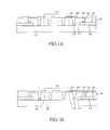
- a wafer-leveled chip packaging method of this embodimentcomprises the following steps. First, referring to FIG. 1A , a silicon wafer 110 having an integrated circuit is provided. The silicon wafer 110 has a first surface 112 on which a plurality of pads 114 is mounted. Then, a plurality of first chips 120 each having at least one pad 122 is attached to the first surface 112 of the silicon wafer 110 with an adhesive 130 , wherein the pad 122 is disposed on a surface opposed to the silicon wafer 110 . Then, a first insulating layer 140 is laminated on the first surface 112 of the silicon wafer 110 .
- first conductive vias 142are connected with the pads 114 of the silicon wafer 110 at the bottom thereof.
- Parts of the bottom of first conductive vias 142are connected with the pads 122 of the first chips 120 at the bottom thereof.
- Parts of first conductive vias 142are connected with a scribe-line region 116 of the silicon wafer 110 at the bottoms thereof.
- a conductive pattern layer 150is formed on the surface of the first insulating layer 140 and is electrically connected with the first conductive vias 142 . Then, a solder mask layer 160 having a pattern is formed on the conductive pattern layer 150 to protect the conductive pattern layer 150 .
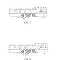
- the wafer 110is wet etched with an HF solution or a mixed solution such as “Isoform Silicon etch solution” manufactured by Micro Image technology Ltd.
- an HF solution or a mixed solutionsuch as “Isoform Silicon etch solution” manufactured by Micro Image technology Ltd.
- a mixed solutionsuch as “Isoform Silicon etch solution” manufactured by Micro Image technology Ltd.
- a second insulating layer 190 made of epoxyis filled in the through holes 180 , having a thickness t1 greater than the thickness t2 of the silicon wafer 110 to protect the parts of the silicon wafer 110 adjacent to the edges of the through holes 180 .
- a plurality of via-holesis formed in the second conducting layer 190 by laser drilling. Then the inner surfaces of these via-holes are metallized to form a plurality of second conductive vias 192 , and each of them has a metallic film 194 . These second conductive vias 192 pass through the through holes 180 and are electrically connected with the first conductive vias 142 .
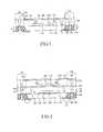
- a plurality of solder balls 210is soldered to the second conductive vias 192 .
- the silicon wafer 110is diced to form a plurality of stackable chip scale package structures 100 .
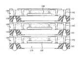
- FIG. 2Three chip scale package structures 100 of this embodiment are stacked as shown in FIG. 2 .
- the transmissions of the electric signal among these chip scale package structuresare achieved primarily by means of the first conductive vias 142 and the second conductive vias 192 .
- the methodis processed thoroughly at the wafer level and is suitable for mass production. Besides, because there is no new processing technology involved, the wafer-leveled chip packaging structure and method thereof of the present invention are easy to accomplish.
- the chip(with a size between 50 ⁇ m to 100 ⁇ m) is carried on a much thicker silicon wafer (with a size about 700 ⁇ m) and both of them are made of silicon, there is no difference in thermal deformation which is caused at the interface between the two different materials with different thermal expansion coefficients respectively, as in the conventional semiconductor electronic packages.
- the thermal stress generated between the chip and the silicon wafercan be reduced, and also, the reliability of the package can be remarkably improved.
- a silicon wafer 110 having an integrated circuit patternis provided.
- the silicon wafer 110has a first surface 112 on which a plurality of pads 114 is mounted.
- a plurality of first chips 120 each having at least one pad 122is attached to the first surface 112 of the silicon wafer 110 with a non-conductive adhesive 130 , wherein the pad 122 is disposed on a surface opposed to the silicon wafer 110 , whereafter a first insulating layer 140 is coated on the first surface 112 of the silicon wafer 110 .
- a plurality of via-holesis formed by laser drilling.
- first conductive vias 142penetrating the first insulating layer 140 .
- Parts of first conductive vias 142are connected with the pads 114 of the silicon wafer 110 at the bottom thereof
- Parts of the bottom of the first conductive vias 142are connected with the pads 122 of the first chips 120 at the bottom thereof
- Parts of first conductive vias 142are connected with a scribe-line region 116 of the silicon wafer 110 at the bottoms thereof.
- a conductive pattern layer 150is formed on the surface of the first insulating layer 140 and is electrically connected with the first conductive vias 142 .
- a solder mask layer 160 having a patternis formed on the conductive pattern layer 150 to protect the conductive pattern layer 150 .
- a plurality of solder balls 170is formed in via-holes 162 of the solder mask layer 160 so that these solder balls 170 are electrically connected with the conductive pattern layer 150 .
- the wafer 110is dry etched to form a plurality of through holes 180 penetrating the scribe-line area 116 of the silicon wafer 110 . As a result, the ends of the first conductive vias 142 in contact with the silicon wafer 110 in the scribe-line area 116 are exposed.
- a second insulating layer 190is then filled in the through holes 180 , having a thickness t1 greater than the thickness t2 of the silicon wafer 110 to protect the parts of the silicon wafer 110 adjacent to the edges of the through holes 180 .
- a plurality of via-holesis formed by laser drilling, and then, a conducting material is filled in these via-holes by electroplating to form a plurality of second conductive vias 192 penetrating the through holes 180 and being electrically connected with the first conductive vias 142 .
- the silicon wafer 110is diced to form a stackable chip scale package structure as shown in FIG. 3 .
- the chip scale package structures of the present inventioncan be stacked as shown in FIG. 2 .
- the solder balls 170are disposed on the inner sides of the first conductive vias 142 , rather than on the orthogonal surface of the first conductive vias 142 or the second conductive vias 192 , the size of the scribe-line area 116 does not have any matter on the solder balls 170 .
- the chip scale package structure of this embodimentis convenient to be connected with an external heat dissipation device, such as a heat sink, providing further heat dissipation efficiency.
- this embodimentdiscloses a wafer-leveled chip packaging method comprising following steps.
- a silicon wafer 110 having a first surface 112is provided.
- An insulating layer 220 and a second conductive pattern layer 230are formed sequentially on the first surface 112 of the silicon wafer 110 .
- an anisotropic conductive glue 240is used to bond a first chip 120 to the silicon wafer 110 with the surface having a circuit pattern formed thereon for additional heat transferring, wherein the second conductive pattern layer 230 formed on the silicon wafer 110 is electrically connected with the first chip 120 .
- a first insulating layer 140is laminated on the silicon wafer 110 .
- a plurality of via-holesis formed by photolithography and a conducting material is filled in the via-holes by electroless plating to form a plurality of first conductive vias 142 which pass through the first insulating layer 140 .
- Parts of the first conductive vias 142are connected with the second conductive pattern layer 230 at the bottom thereof.
- Parts of the first conductive vias 142are connected with a scribe-line region 116 of the silicon wafer 110 at the bottoms thereof.
- a conductive pattern layer 150is formed on the surface of the first insulating layer 140 and is electrically connected with the first conductive vias 142 .
- a protection layer 250 having a patternis formed on the conductive pattern layer 150 to protect the conductive pattern layer 150 .
- a non-conductive adhesive 260is used to bond a plurality of second chips 270 each having at least one pad 272 to the protection layer 250 . These pads 272 are disposed on the surface opposed the protection layer 250 .
- a fourth insulating layer 280is pressed on the second chips 270 .
- a plurality of via-holesis formed by laser drilling and a conducting material is filled in the via-holes by electroplating to form a plurality of fourth conductive vias 282 which pass through the fourth insulating layer 280 .
- Parts of fourth conductive vias 282are connected with the pads 272 of the second chips 270 at the bottom thereof. Parts of fourth conductive vias 282 are connected with a conductive pattern layer 150 at the bottoms thereof.
- a third conducting layer 290is formed on the fourth conducting layer 280 and is electrically connected with the fourth conductive vias 282 .
- a protection layer 310 having a patternis formed on the third conductive pattern layer 290 .
- the back face of the silicon wafer 110is wet etched with an HF solution to form a plurality of through holes 180 penetrating the silicon wafer 110 .
- the through holes 180are disposed outside the region where the first chip 120 is carried so that the ends of those first conductive vias 142 being in contact with the silicon wafer 110 with in that region are exposed.
- a second insulating layer 190 of epoxyis filled in the through holes 180 .
- a plurality of via-holesis then formed in the second insulating layer 190 by laser drilling and a conducting material is filled in the via-holes by electroplating to form a plurality of second conductive vias 192 .
- These second conductive vias 192pass through the through holes 180 and are electrically connected with the first conductive vias 142 .
- a plurality of solder balls 210is soldered to the inner sides of the second conductive vias 192 .
- the silicon wafer 110is diced to form a stackable chip scale package structure as shown in FIG. 4 .
- the chip scale package structures of the present inventioncan be stacked. Furthermore, because two or more layers of chip can be stacked in a unit package area, the chip density of the package can effectively increase.
- the methodis processed thoroughly at the wafer level and is suitable for mass production. Besides, due to no new processing technology being involved, the wafer-leveled chip packaging structure and method thereof of the present invention are easy to accomplish. In addition, because the chip is carried on silicon wafer, the thermal stress generated between the chip and the silicon wafer can be reduced, and also, the reliability of the package can be remarkably improved.
Landscapes
- Engineering & Computer Science (AREA)
- Microelectronics & Electronic Packaging (AREA)
- Power Engineering (AREA)
- Computer Hardware Design (AREA)
- Physics & Mathematics (AREA)
- Condensed Matter Physics & Semiconductors (AREA)
- General Physics & Mathematics (AREA)
- Manufacturing & Machinery (AREA)
- Ceramic Engineering (AREA)
- Internal Circuitry In Semiconductor Integrated Circuit Devices (AREA)
- Production Of Multi-Layered Print Wiring Board (AREA)
Abstract
Description
- This application is a continuation of co-pending U.S. application Ser. No. 13/533,251, filed on Jun. 26, 2012, which is a continuation of U.S. application Ser. No. 11/905,869, filed on Oct. 5, 2007, now U.S. Pat. No. 8,314,482, which is a continuation of U.S. application Ser. No. 11/186,840, filed Jul. 22, 2005, now U.S. Pat. No. 7,294,920.
- 1. Field of the Invention
- The present invention relates to a wafer-leveled chip packaging structure and method thereof, and more particularly, to a wafer-leveled chip packaging structure and method thereof for forming a wafer-leveled chip package by a wafer-leveled fabrication process.
- 2. Description of the Related Art
- A semiconductor package chip is generally encapsulated into a plastic or ceramic material, which refers to level one packaging. As a rule, the package is required to support and protect the chip, increase the heat dissipation efficiency, and provide a system for distributing the electrical power and signals input and/or output the chip. Sometimes, the package is also used for testing the performance of the chip.
- An important indication to verify the advancement of the chip packaging techniques is to the ratio of the package area to the chip area. The closer the ratio to 1, the better the technique is. Several well-known chip-packaging techniques are as follows. (1) Dual-in-line packages (DIP) are initially adopted for packaging memory chips. However, the size of the DIP is much larger than the chip and occupies a significant portion of the mounting areas. Thus, the DIP is insufficient. (2) Thin-small-outline packages (TSOP) provide leads around the package chip. The TSOP is suitable for mounting lines on the surface of a PCB by surface mount technique (SMT). Thus, TSOP is reliable, suitable for high frequency application and easy to operate with. (3) Ball grid array (BGA) packages have been widely used in a large-scale integrated circuit package application such as the memory of the notebook computers. Although the power consumption increases as a result of the BGA package technique, the chips packaged therein have improved electrical and thermal performances, thus improving the reliability thereof. Also, though the number of 1/0 leads increases, the space between leads of the BGA package remains unchanged so as to be capable of increasing the product yield. Furthermore, the thickness and weight of the memory packaged are reduced. Besides, the signal transmission delays of the chips become less significant and thus the applicable frequency domain of the BGA package is broadened. (4) Chip scale packages (CSP) can reduce the ratio of the package area to the chip area to be less than 1.5. Comparing to the BGA package, the volume of a CSP memory product is smaller than that of a BGA package memory product. Besides, the CSP can have higher capacity but better heat dissipation than the BGA package. In addition, due to its significantly increased electrical performance, reliability and high system stability, the CSP has become the popular memory package technique for packaging a variety of products, such as DRAM.
- Specifically speaking, the chip scale package (CSP) generally comprises a chip attaching to the surface of a substrate, wherein the substrate includes plural external contacts for electrically connecting the external device with the chip packaged therein. The substrate for the CSP comprises a flexible material such as a polymer tape, a rigid material such as silicon, ceramics or glass. The external contacts may include solder balls arranged in a dense manner such as the ball grid array (BGA) or a fine ball grid array (FBGA). Such high-density arrays can provide the chip scale package with a high input/output capability. For example, the FBGA of the CSP can have hundreds of solder balls in a unit area.
- In addition, the form of central leads of memory chip packaged with the CSP can effectively shorten the signal transmitting paths. Thus, the CSP can lower the degree of the signal attenuation and increase the anti-interference and anti-noise performances of the chip packaged therein. As a result, the access time of the CSP is faster than the BGA by about 15%to 20%.
- In the CSP, the memory chip is soldered to the PCB with plural solder balls which have large contact areas with the PCB, the heat generated by the memory chip during the operation can be easily transferred to the PCB for heat dissipation. On the other hand, the memory chip of the TSOP is soldered to the PCB with the leads of the chip. Therefore, the contact area between the solder and the PCB is much smaller and it is difficult to transfer heat from the chip to the PCB. Besides, the CSP can dissipate heat by its back face efficiently and be constructed compactly, whereby much unnecessary electric power consumption can be eliminated. Correspondingly, the chip packaged with the CSP can have low power consumption and lowered working temperature in comparison with the chips packaged with other package technology.
- In the industry, especially in the wireless communication industry, the recent development of the chip scale packages is focused not only on reducing power consumption and packaging volume, but also on increasing the packaging density of the memory chip and performance. Therefore, stackability of the chip scale package is one of the solutions for increasing the packaging density of the memory chip and providing the chip package structure and method thereof with stackable chip scale packages are the objects of the present invention.
- An object of the present invention is to provide a wafer-leveled chip packaging method having stackable function and being processed thoroughly at the wafer level so as to reduce the fabrication cost and increase the mass production yield.
- Another object of the present invention to provide a wafer-leveled chip packaging method in which the packaging process for a chip continues after another chip is carried on a wafer so as to integrate the functions of all the chips packaged. Also, the resulting wafer-leveled chip package of the present invention has stackable function so as to increase the chip density of a unit area.
- A further object of the present invention is to provide a wafer-leveled chip package structure of a wafer-leveled chip package having stackable function so as to increase the chip density of a unit area. The chip package structure can be fabricated thoroughly at the wafer level so as to reduce the fabrication cost and increase the mass production yield.
- To attain the aforesaid objects, a wafer-leveled chip packaging method according to the present invention comprises the steps of: (A) providing a wafer having an integrated circuit, wherein the wafer has a first surface on which a plurality of pads is mounted; (B) forming a first insulating layer on the first surface of the wafer; (C) forming a plurality of first conductive vias penetrating the first insulating layer, wherein parts of the first conductive vias are connected with the pads; (D) forming a first conductive pattern layer on the surface of the first insulating layer, wherein the first conductive pattern layer is electrically connected with the first conductive vias; (E) forming a plurality of through holes penetrating the wafer so that parts of the first conductive vias contacting with the wafer are exposed; (F) filling a second insulating layer in the through holes; and (G) forming a plurality of second conductive vias in the second insulating layer within the through holes, and the second conductive vias are electrically connected with the first conductive vias.
- To attain the aforesaid objects, a wafer-leveled chip packaging method according to the present invention comprises the steps of: (A) providing a wafer having a first surface; (B) attaching at least one first chip having a plurality of pads to the first surface of the wafer; (C) forming a first insulating layer on the first surface of the wafer; (D) forming a plurality of first conductive vias penetrating the first insulating layer, wherein parts of the first conductive vias are electrically connected with the pads of the first chip; (E) forming a first conductive pattern layer on the surface of the first insulating layer, wherein the first conductive pattern layer is electrically connected with the first conductive vias; (F) forming a plurality of through holes penetrating the wafer so that parts of the first conductive vias contacting with the wafer are exposed; (G) filling a second insulating layer in the through holes; and (H) forming a plurality of second conductive vias in the second insulating layer within the through holes, and the second conductive vias are electrically connected with the first conductive vias.
- To attain the aforesaid objects, a wafer-leveled chip packaging method according to the present invention comprises the steps of: a wafer having a first surface, on which an integrated circuit pattern and a plurality of pads are formed, and a plurality of through holes penetrating the wafer, wherein a second insulating layer is filled in the through holes and at least one second conducting via passes through the second insulating layer; a plurality of first chips each having at least one pad on the first surface of the wafer, wherein the pads being mounted on the surface of the first chip which is opposed to the wafer; a first insulating layer formed on the first surface of the wafer, having a plurality of first conductive vias penetrating the first insulating layer, wherein the first insulating layer covers the first chips and the integrated circuit pattern of the wafer; and a conductive pattern layer formed on a surface opposed to the wafer of the first insulating layer, and the conductive pattern layer is electrically connected with the first conductive vias; wherein parts of the first conductive vias are connected with the pads of the wafer, parts of the first conductive vias are connected with the pads of the first chips and part of the first conductive vias are connected with the second conductive vias in the through holes.
- In the wafer-leveled chip packaging method according to the present invention, the wafer is either a wafer with an integrated circuit thereon or a wafer without an integrated circuit. In the wafer-leveled chip packaging structure and method thereof according to the present invention, the quantity of chip layers in stack on the wafer is not specifically defined, which can be a form of either having a plurality of first chips attached directly to the first surface of the wafer or having other chips stacked on the first chip by the way of “build-up”. In the wafer-leveled chip packaging method according to the present invention, the method to attach the first chip is case-sensitive. In the case of the wafer with an integrated circuit pattern, it is preferable to attach the first chip to the first surface of the wafer with a non-conductive adhesive, wherein the pads of the first chip is disposed on the surface which is opposed to the wafer. The first chips can also be attached to the first surface of the wafer with a thermal adhesive so as to enhance the ability of heat dissipation. In the case of the wafer with an integrated circuit pattern, it is preferable to form an insulating layer and a second conductive pattern layer on the first surface of the wafer first, then attaching the first chip to the first surface of the wafer with an anisotropic conductive glue or a non-conductive glue, wherein the pads of the first chip are disposed on the surface facing the first surface of the wafer and electrically connected with the second conductive pattern layer. In addition, the pads of the first chip can alternatively be disposed on a surface opposed to the wafer when the first chip attaches to the first surface of the wafer. In the wafer-leveled chip packaging method according to the present invention, the formation method of the first insulating layer is not limited, and is preferably by laminating or coating. The first conductive vias and the second conductive vias are preferably formed by generating the via-holes by laser or photolithography first, and then filling the via-holes with conducting material by electroplating, electroless plating or the combination thereof. Alternatively, the first conductive vias and the second conductive vias can be formed by generating the via-holes by laser drilling first, and then metalizing the inner surfaces of the via-holes by sputtering or evaporation. The through holes are preferably formed by wet etching or dry etching. In the wafer-leveled chip packaging structure according to the present invention, the second insulating layer is preferably thicker than the wafer to protect the wafer. Even so, the thickness of the second conducting layer can be equal or less than that of the wafer to meet the requirement for a thinner package.
- In the wafer-leveled chip packaging structure and method thereof according to the present invention, it is preferable to further comprise a third insulating layer having a pattern formed on the conductive pattern layer to protect the conductive pattern layer after the formation of the conductive pattern layer on the surface of the first insulating layer. The third insulating layer can preferably be a solder mask layer or a protection layer. When the third insulating layer is a solder mask layer, a plurality of solder balls, needle pins or other like structures can be formed on the third insulating layer and be electrically connected with the conductive pattern layer. Alternatively, the solder balls, needle pins or the like of the present invention can also be formed on the second conductive vias. When the third insulating layer is a protection layer, a plurality of second chips can be carried on the surface of the third insulating layer, a fourth insulating layer then covers the second chips, and a plurality of fourth conductive vias penetrating the fourth insulating layer are formed.
- In the wafer-leveled chip packaging structure and method thereof according to the present invention, the wafer can be preferably diced to form a plurality of chip scale package structures. Because the two sides of the resulting package structure both have conductive patterns that can be connected with the electric circuits of the wafer or of the other chips, the resulting package structures of the present invention can be stacked.
- Additional features and advantages of the present invention will be set forth in part in the description which follows, and in part will be obvious from the description, or may be learned by practice of the present invention. The features and advantages of the present invention will be realized and attained by means of the elements and combinations particularly pointed out in the henceforth appended claims.
- It is to be understood that both the foregoing general description and the following detailed description are exemplary and explanatory only and are not restrictive of the present invention, as claimed.
- The accompanying drawings, which are incorporated in and constitute a part of this specification, illustrate several embodiments of the present invention and together with the description, serve to explain the principles of the present invention.
FIGS. 1A through 1G are flowcharts illustrating the wafer-leveled chip packaging method according to a preferred embodiment of the present invention;FIG. 2 is a schematic view of a stack of wafer-leveled chip package structures according to a preferred embodiment formed by the wafer-leveled chip packaging method as shown inFIGS. 1A through 1G ;FIG. 3 is a schematic view of a preferred embodiment using the wafer-leveled chip packaging method according to the present invention;FIG. 4 is a schematic view of another preferred embodiment using the wafer-leveled chip packaging method according to the present invention;- Reference will now be made in detail to present embodiments of the present invention, examples of which are illustrated in the accompanying drawings. Where ever possible, the same reference numbers will be used throughout the drawings to refer to the same or like parts.
- To illustrate the present invention, three preferred embodiments are described now.
- A wafer-leveled chip packaging method of this embodiment comprises the following steps. First, referring to
FIG. 1A , asilicon wafer 110 having an integrated circuit is provided. Thesilicon wafer 110 has afirst surface 112 on which a plurality ofpads 114 is mounted. Then, a plurality offirst chips 120 each having at least onepad 122 is attached to thefirst surface 112 of thesilicon wafer 110 with an adhesive130, wherein thepad 122 is disposed on a surface opposed to thesilicon wafer 110. Then, a first insulatinglayer 140 is laminated on thefirst surface 112 of thesilicon wafer 110. Next, a plurality of via-holes is formed by laser or photolithography, and after that a conducting material is filled in the via-holes by electroplating, electroless plating or the combination thereof so as to form a plurality of firstconductive vias 142 penetrating the first insulatinglayer 140. Parts of firstconductive vias 142 are connected with thepads 114 of thesilicon wafer 110 at the bottom thereof. Parts of the bottom of firstconductive vias 142 are connected with thepads 122 of thefirst chips 120 at the bottom thereof. Parts of firstconductive vias 142 are connected with a scribe-line region 116 of thesilicon wafer 110 at the bottoms thereof. Then, aconductive pattern layer 150 is formed on the surface of the first insulatinglayer 140 and is electrically connected with the firstconductive vias 142. Then, asolder mask layer 160 having a pattern is formed on theconductive pattern layer 150 to protect theconductive pattern layer 150. - Referring now to
FIG. 1B , thewafer 110 is wet etched with an HF solution or a mixed solution such as “Isoform Silicon etch solution” manufactured by Micro Image technology Ltd. In order to form a plurality of throughholes 180 penetrating the scribe-line area 116 of thesilicon wafer 110. As a result, the ends of the firstconductive vias 142 that are in contact with thesilicon wafer 110 in the scribe-line area 116 are exposed. - Referring to
FIG. 1C , a second insulatinglayer 190 made of epoxy is filled in the throughholes 180, having a thickness t1 greater than the thickness t2 of thesilicon wafer 110 to protect the parts of thesilicon wafer 110 adjacent to the edges of the throughholes 180. - Referring to
FIG. 1D andFIG. 1E , a plurality of via-holes is formed in thesecond conducting layer 190 by laser drilling. Then the inner surfaces of these via-holes are metallized to form a plurality of secondconductive vias 192, and each of them has ametallic film 194. These secondconductive vias 192 pass through the throughholes 180 and are electrically connected with the firstconductive vias 142. - Referring to
FIG. 1F , a plurality ofsolder balls 210 is soldered to the secondconductive vias 192. Finally, referring toFIG. 1G , thesilicon wafer 110 is diced to form a plurality of stackable chipscale package structures 100. - Three chip
scale package structures 100 of this embodiment are stacked as shown inFIG. 2 . The transmissions of the electric signal among these chip scale package structures are achieved primarily by means of the firstconductive vias 142 and the secondconductive vias 192. The method is processed thoroughly at the wafer level and is suitable for mass production. Besides, because there is no new processing technology involved, the wafer-leveled chip packaging structure and method thereof of the present invention are easy to accomplish. In addition, because the chip (with a size between 50 μm to 100 μm) is carried on a much thicker silicon wafer (with a size about 700 μm) and both of them are made of silicon, there is no difference in thermal deformation which is caused at the interface between the two different materials with different thermal expansion coefficients respectively, as in the conventional semiconductor electronic packages. Thus, the thermal stress generated between the chip and the silicon wafer can be reduced, and also, the reliability of the package can be remarkably improved. - Referring now to
FIG. 3 , the second embodiment of a wafer-leveled chip packaging method of the present invention is disclosed, which comprises the following steps. Asilicon wafer 110 having an integrated circuit pattern is provided. Thesilicon wafer 110 has afirst surface 112 on which a plurality ofpads 114 is mounted. Then, a plurality offirst chips 120 each having at least onepad 122 is attached to thefirst surface 112 of thesilicon wafer 110 with anon-conductive adhesive 130, wherein thepad 122 is disposed on a surface opposed to thesilicon wafer 110, whereafter a first insulatinglayer 140 is coated on thefirst surface 112 of thesilicon wafer 110. Then, a plurality of via-holes is formed by laser drilling. - Next, a conducting material is filled in the via-holes by electroplating or electroless plating so as to form a plurality of first
conductive vias 142 penetrating the first insulatinglayer 140. Parts of firstconductive vias 142 are connected with thepads 114 of thesilicon wafer 110 at the bottom thereof Parts of the bottom of the firstconductive vias 142 are connected with thepads 122 of thefirst chips 120 at the bottom thereof Parts of firstconductive vias 142 are connected with a scribe-line region 116 of thesilicon wafer 110 at the bottoms thereof. Then, aconductive pattern layer 150 is formed on the surface of the first insulatinglayer 140 and is electrically connected with the firstconductive vias 142. Subsequently, asolder mask layer 160 having a pattern is formed on theconductive pattern layer 150 to protect theconductive pattern layer 150. Then, a plurality of solder balls170 is formed in via-holes 162 of thesolder mask layer 160 so that these solder balls170 are electrically connected with theconductive pattern layer 150. Thewafer 110 is dry etched to form a plurality of throughholes 180 penetrating the scribe-line area 116 of thesilicon wafer 110. As a result, the ends of the firstconductive vias 142 in contact with thesilicon wafer 110 in the scribe-line area 116 are exposed. A second insulatinglayer 190 is then filled in the throughholes 180, having a thickness t1 greater than the thickness t2 of thesilicon wafer 110 to protect the parts of thesilicon wafer 110 adjacent to the edges of the throughholes 180. A plurality of via-holes is formed by laser drilling, and then, a conducting material is filled in these via-holes by electroplating to form a plurality of secondconductive vias 192 penetrating the throughholes 180 and being electrically connected with the firstconductive vias 142. Finally, thesilicon wafer 110 is diced to form a stackable chip scale package structure as shown inFIG. 3 . - Because the two sides of the chip scale package structure both have conductive patterns that can be connected with the electric circuits of the wafer or of the other chips, the chip scale package structures of the present invention can be stacked as shown in
FIG. 2 . In this embodiment, because the solder balls170 are disposed on the inner sides of the firstconductive vias 142, rather than on the orthogonal surface of the firstconductive vias 142 or the secondconductive vias 192, the size of the scribe-line area 116 does not have any matter on the solder balls170. Furthermore, because the silicon wafer substrate faces outward (as opposed to the solder balls), the chip scale package structure of this embodiment is convenient to be connected with an external heat dissipation device, such as a heat sink, providing further heat dissipation efficiency. - Referring to
FIG. 4 , this embodiment discloses a wafer-leveled chip packaging method comprising following steps. Asilicon wafer 110 having afirst surface 112 is provided. An insulatinglayer 220 and a secondconductive pattern layer 230 are formed sequentially on thefirst surface 112 of thesilicon wafer 110. Then, an anisotropicconductive glue 240 is used to bond afirst chip 120 to thesilicon wafer 110 with the surface having a circuit pattern formed thereon for additional heat transferring, wherein the secondconductive pattern layer 230 formed on thesilicon wafer 110 is electrically connected with thefirst chip 120. A first insulatinglayer 140 is laminated on thesilicon wafer 110. Then, a plurality of via-holes is formed by photolithography and a conducting material is filled in the via-holes by electroless plating to form a plurality of firstconductive vias 142 which pass through the first insulatinglayer 140. Parts of the firstconductive vias 142 are connected with the secondconductive pattern layer 230 at the bottom thereof. Parts of the firstconductive vias 142 are connected with a scribe-line region 116 of thesilicon wafer 110 at the bottoms thereof. Aconductive pattern layer 150 is formed on the surface of the first insulatinglayer 140 and is electrically connected with the firstconductive vias 142. Aprotection layer 250 having a pattern is formed on theconductive pattern layer 150 to protect theconductive pattern layer 150. Anon-conductive adhesive 260 is used to bond a plurality ofsecond chips 270 each having at least onepad 272 to theprotection layer 250. Thesepads 272 are disposed on the surface opposed theprotection layer 250. A fourth insulatinglayer 280 is pressed on thesecond chips 270. A plurality of via-holes is formed by laser drilling and a conducting material is filled in the via-holes by electroplating to form a plurality of fourthconductive vias 282 which pass through the fourth insulatinglayer 280. Parts of fourthconductive vias 282 are connected with thepads 272 of thesecond chips 270 at the bottom thereof. Parts of fourthconductive vias 282 are connected with aconductive pattern layer 150 at the bottoms thereof. Athird conducting layer 290 is formed on thefourth conducting layer 280 and is electrically connected with the fourthconductive vias 282. Aprotection layer 310 having a pattern is formed on the thirdconductive pattern layer 290. The back face of thesilicon wafer 110 is wet etched with an HF solution to form a plurality of throughholes 180 penetrating thesilicon wafer 110. The throughholes 180 are disposed outside the region where thefirst chip 120 is carried so that the ends of those firstconductive vias 142 being in contact with thesilicon wafer 110 with in that region are exposed. A second insulatinglayer 190 of epoxy is filled in the throughholes 180. A plurality of via-holes is then formed in the second insulatinglayer 190 by laser drilling and a conducting material is filled in the via-holes by electroplating to form a plurality of secondconductive vias 192. These secondconductive vias 192 pass through the throughholes 180 and are electrically connected with the firstconductive vias 142. A plurality ofsolder balls 210 is soldered to the inner sides of the secondconductive vias 192. Finally, thesilicon wafer 110 is diced to form a stackable chip scale package structure as shown inFIG. 4 . - Because the two sides of the chip scale package structure both have conductive patterns that can be connected with the electric circuits of the wafer or of the other chips, the chip scale package structures of the present invention can be stacked. Furthermore, because two or more layers of chip can be stacked in a unit package area, the chip density of the package can effectively increase. In addition, the method is processed thoroughly at the wafer level and is suitable for mass production. Besides, due to no new processing technology being involved, the wafer-leveled chip packaging structure and method thereof of the present invention are easy to accomplish. In addition, because the chip is carried on silicon wafer, the thermal stress generated between the chip and the silicon wafer can be reduced, and also, the reliability of the package can be remarkably improved.
- Other embodiments of the present invention will be apparent to those skilled in the art from consideration of the specification and practice of the present invention disclosed herein. It is intended that the specification and examples be considered as exemplary only, with a true scope and spirit of the present invention being indicated by the following claims.
Claims (14)
Priority Applications (2)
| Application Number | Priority Date | Filing Date | Title |
|---|---|---|---|
| US14/083,377US9059181B2 (en) | 2004-07-23 | 2013-11-18 | Wafer leveled chip packaging structure and method thereof |
| US14/740,184US9601474B2 (en) | 2005-07-22 | 2015-06-15 | Electrically stackable semiconductor wafer and chip packages |
Applications Claiming Priority (7)
| Application Number | Priority Date | Filing Date | Title |
|---|---|---|---|
| TW093122038 | 2004-07-23 | ||
| TW093122038ATWI250596B (en) | 2004-07-23 | 2004-07-23 | Wafer-level chip scale packaging method |
| TW93122038A | 2004-07-23 | ||
| US11/186,840US7294920B2 (en) | 2004-07-23 | 2005-07-22 | Wafer-leveled chip packaging structure and method thereof |
| US11/905,869US8314482B2 (en) | 2004-07-23 | 2007-10-05 | Semiconductor package device |
| US13/533,251US8587091B2 (en) | 2004-07-23 | 2012-06-26 | Wafer-leveled chip packaging structure and method thereof |
| US14/083,377US9059181B2 (en) | 2004-07-23 | 2013-11-18 | Wafer leveled chip packaging structure and method thereof |
Related Parent Applications (1)
| Application Number | Title | Priority Date | Filing Date |
|---|---|---|---|
| US13/533,251ContinuationUS8587091B2 (en) | 2004-07-23 | 2012-06-26 | Wafer-leveled chip packaging structure and method thereof |
Related Child Applications (1)
| Application Number | Title | Priority Date | Filing Date |
|---|---|---|---|
| US14/740,184ContinuationUS9601474B2 (en) | 2005-07-22 | 2015-06-15 | Electrically stackable semiconductor wafer and chip packages |
Publications (2)
| Publication Number | Publication Date |
|---|---|
| US20140217587A1true US20140217587A1 (en) | 2014-08-07 |
| US9059181B2 US9059181B2 (en) | 2015-06-16 |
Family
ID=35657792
Family Applications (5)
| Application Number | Title | Priority Date | Filing Date |
|---|---|---|---|
| US11/186,840Active2026-01-24US7294920B2 (en) | 2004-07-23 | 2005-07-22 | Wafer-leveled chip packaging structure and method thereof |
| US11/785,612Active2025-10-20US7528009B2 (en) | 2004-07-23 | 2007-04-19 | Wafer-leveled chip packaging structure and method thereof |
| US11/905,869Active2026-01-31US8314482B2 (en) | 2004-07-23 | 2007-10-05 | Semiconductor package device |
| US13/533,251Expired - LifetimeUS8587091B2 (en) | 2004-07-23 | 2012-06-26 | Wafer-leveled chip packaging structure and method thereof |
| US14/083,377Expired - LifetimeUS9059181B2 (en) | 2004-07-23 | 2013-11-18 | Wafer leveled chip packaging structure and method thereof |
Family Applications Before (4)
| Application Number | Title | Priority Date | Filing Date |
|---|---|---|---|
| US11/186,840Active2026-01-24US7294920B2 (en) | 2004-07-23 | 2005-07-22 | Wafer-leveled chip packaging structure and method thereof |
| US11/785,612Active2025-10-20US7528009B2 (en) | 2004-07-23 | 2007-04-19 | Wafer-leveled chip packaging structure and method thereof |
| US11/905,869Active2026-01-31US8314482B2 (en) | 2004-07-23 | 2007-10-05 | Semiconductor package device |
| US13/533,251Expired - LifetimeUS8587091B2 (en) | 2004-07-23 | 2012-06-26 | Wafer-leveled chip packaging structure and method thereof |
Country Status (2)
| Country | Link |
|---|---|
| US (5) | US7294920B2 (en) |
| TW (1) | TWI250596B (en) |
Cited By (3)
| Publication number | Priority date | Publication date | Assignee | Title |
|---|---|---|---|---|
| US20120286400A1 (en)* | 2007-12-27 | 2012-11-15 | Stats Chippac, Ltd. | Semiconductor Device with Optical Sensor and Method of Forming Interconnect Structure on Front and Backside of the Device |
| CN106449555A (en)* | 2016-12-09 | 2017-02-22 | 华进半导体封装先导技术研发中心有限公司 | Chip packaging process and chip packaging structure |
| TWI779972B (en)* | 2021-08-31 | 2022-10-01 | 南亞科技股份有限公司 | Semiconductor package structure and method for preparing the same |
Families Citing this family (96)
| Publication number | Priority date | Publication date | Assignee | Title |
|---|---|---|---|---|
| TWI250596B (en)* | 2004-07-23 | 2006-03-01 | Ind Tech Res Inst | Wafer-level chip scale packaging method |
| TWI250629B (en)* | 2005-01-12 | 2006-03-01 | Ind Tech Res Inst | Electronic package and fabricating method thereof |
| KR100629498B1 (en)* | 2005-07-15 | 2006-09-28 | 삼성전자주식회사 | Micro-Packages, Multi-Stack Micro-Packages, and Methods for Making the Same |
| US9601474B2 (en)* | 2005-07-22 | 2017-03-21 | Invensas Corporation | Electrically stackable semiconductor wafer and chip packages |
| TWI284402B (en)* | 2005-12-30 | 2007-07-21 | Advanced Semiconductor Eng | Build-up package and method of an optoelectronic chip |
| SG135074A1 (en) | 2006-02-28 | 2007-09-28 | Micron Technology Inc | Microelectronic devices, stacked microelectronic devices, and methods for manufacturing such devices |
| KR100832845B1 (en)* | 2006-10-03 | 2008-05-28 | 삼성전자주식회사 | Semiconductor package structure and manufacturing method thereof |
| US8174119B2 (en)* | 2006-11-10 | 2012-05-08 | Stats Chippac, Ltd. | Semiconductor package with embedded die |
| TWI394244B (en)* | 2006-12-29 | 2013-04-21 | Xintec Inc | Chip package module |
| US7781877B2 (en)* | 2007-08-07 | 2010-08-24 | Micron Technology, Inc. | Packaged integrated circuit devices with through-body conductive vias, and methods of making same |
| US7956453B1 (en)* | 2008-01-16 | 2011-06-07 | Amkor Technology, Inc. | Semiconductor package with patterning layer and method of making same |
| WO2009107742A1 (en)* | 2008-02-28 | 2009-09-03 | 日本電気株式会社 | Semiconductor device |
| US8026740B2 (en) | 2008-03-21 | 2011-09-27 | Micron Technology, Inc. | Multi-level signaling for low power, short channel applications |
| US8072079B2 (en)* | 2008-03-27 | 2011-12-06 | Stats Chippac, Ltd. | Through hole vias at saw streets including protrusions or recesses for interconnection |
| US8021907B2 (en)* | 2008-06-09 | 2011-09-20 | Stats Chippac, Ltd. | Method and apparatus for thermally enhanced semiconductor package |
| TWI453877B (en)* | 2008-11-07 | 2014-09-21 | Advanced Semiconductor Eng | Structure and process of embedded chip package |
| US8299566B2 (en) | 2008-08-08 | 2012-10-30 | International Business Machines Corporation | Through wafer vias and method of making same |
| US8138036B2 (en) | 2008-08-08 | 2012-03-20 | International Business Machines Corporation | Through silicon via and method of fabricating same |
| US8384224B2 (en) | 2008-08-08 | 2013-02-26 | International Business Machines Corporation | Through wafer vias and method of making same |
| US8035198B2 (en)* | 2008-08-08 | 2011-10-11 | International Business Machines Corporation | Through wafer via and method of making same |
| US7678696B2 (en)* | 2008-08-08 | 2010-03-16 | International Business Machines Corporation | Method of making through wafer vias |
| US7989950B2 (en)* | 2008-08-14 | 2011-08-02 | Stats Chippac Ltd. | Integrated circuit packaging system having a cavity |
| US8823160B2 (en)* | 2008-08-22 | 2014-09-02 | Stats Chippac Ltd. | Integrated circuit package system having cavity |
| US8259461B2 (en) | 2008-11-25 | 2012-09-04 | Micron Technology, Inc. | Apparatus for bypassing faulty connections |
| US20100187651A1 (en) | 2009-01-26 | 2010-07-29 | Stmicroelectronics Asia Pacific Pte Ltd. | Integrated circuit package and method of forming the same |
| US8652697B2 (en)* | 2009-02-25 | 2014-02-18 | Bloom Energy Corporation | Controlling a fuel cell system based on fuel cell impedance characteristic |
| US8643164B2 (en)* | 2009-06-11 | 2014-02-04 | Broadcom Corporation | Package-on-package technology for fan-out wafer-level packaging |
| TWI388038B (en)* | 2009-07-23 | 2013-03-01 | Ind Tech Res Inst | Structure and fabrication method of a sensing device |
| US8895358B2 (en)* | 2009-09-11 | 2014-11-25 | Stats Chippac, Ltd. | Semiconductor device and method of forming cavity in PCB containing encapsulant or dummy die having CTE similar to CTE of large array WLCSP |
| US8569894B2 (en) | 2010-01-13 | 2013-10-29 | Advanced Semiconductor Engineering, Inc. | Semiconductor package with single sided substrate design and manufacturing methods thereof |
| US8320134B2 (en) | 2010-02-05 | 2012-11-27 | Advanced Semiconductor Engineering, Inc. | Embedded component substrate and manufacturing methods thereof |
| TWI411075B (en) | 2010-03-22 | 2013-10-01 | Advanced Semiconductor Eng | Semiconductor package and manufacturing method thereof |
| US8455300B2 (en) | 2010-05-25 | 2013-06-04 | Stats Chippac Ltd. | Integrated circuit package system with embedded die superstructure and method of manufacture thereof |
| US8482111B2 (en) | 2010-07-19 | 2013-07-09 | Tessera, Inc. | Stackable molded microelectronic packages |
| US8895440B2 (en) | 2010-08-06 | 2014-11-25 | Stats Chippac, Ltd. | Semiconductor die and method of forming Fo-WLCSP vertical interconnect using TSV and TMV |
| TWI501365B (en)* | 2010-10-13 | 2015-09-21 | Ind Tech Res Inst | Package unit, stacking structure thereof and manufacturing method thereof |
| US8263435B2 (en) | 2010-10-28 | 2012-09-11 | Stats Chippac, Ltd. | Semiconductor device and method of stacking semiconductor die in mold laser package interconnected by bumps and conductive vias |
| US9406658B2 (en) | 2010-12-17 | 2016-08-02 | Advanced Semiconductor Engineering, Inc. | Embedded component device and manufacturing methods thereof |
| JP5514134B2 (en)* | 2011-02-14 | 2014-06-04 | ルネサスエレクトロニクス株式会社 | Manufacturing method of semiconductor device |
| US8273604B2 (en)* | 2011-02-22 | 2012-09-25 | STAT ChipPAC, Ltd. | Semiconductor device and method of forming WLCSP structure using protruded MLP |
| US8525344B2 (en)* | 2011-02-24 | 2013-09-03 | Stats Chippac, Ltd. | Semiconductor device and method of forming bond wires between semiconductor die contact pads and conductive TOV in peripheral area around semiconductor die |
| US8487426B2 (en) | 2011-03-15 | 2013-07-16 | Advanced Semiconductor Engineering, Inc. | Semiconductor package with embedded die and manufacturing methods thereof |
| KR101128063B1 (en) | 2011-05-03 | 2012-04-23 | 테세라, 인코포레이티드 | Package-on-package assembly with wire bonds to encapsulation surface |
| US8604576B2 (en)* | 2011-07-19 | 2013-12-10 | Opitz, Inc. | Low stress cavity package for back side illuminated image sensor, and method of making same |
| KR20140053175A (en)* | 2011-08-11 | 2014-05-07 | 도쿄엘렉트론가부시키가이샤 | Semiconductor device manufacturing method, semiconductor device, and jig for forming wiring |
| US20130049214A1 (en)* | 2011-08-29 | 2013-02-28 | Infineon Technologies Ag | Method of processing at least one die and die arrangement |
| US8513057B2 (en) | 2011-09-16 | 2013-08-20 | Stats Chippac Ltd. | Integrated circuit packaging system with routable underlayer and method of manufacture thereof |
| US8664756B2 (en)* | 2012-07-24 | 2014-03-04 | Medtronic, Inc. | Reconstituted wafer package with high voltage discrete active dice and integrated field plate for high temperature leakage current stability |
| US8836136B2 (en) | 2011-10-17 | 2014-09-16 | Invensas Corporation | Package-on-package assembly with wire bond vias |
| US11445617B2 (en)* | 2011-10-31 | 2022-09-13 | Unimicron Technology Corp. | Package structure and manufacturing method thereof |
| TWI463633B (en)* | 2011-12-30 | 2014-12-01 | Ind Tech Res Inst | Chip package structure |
| US8946757B2 (en) | 2012-02-17 | 2015-02-03 | Invensas Corporation | Heat spreading substrate with embedded interconnects |
| US8372741B1 (en) | 2012-02-24 | 2013-02-12 | Invensas Corporation | Method for package-on-package assembly with wire bonds to encapsulation surface |
| US8835228B2 (en) | 2012-05-22 | 2014-09-16 | Invensas Corporation | Substrate-less stackable package with wire-bond interconnect |
| KR101947722B1 (en)* | 2012-06-07 | 2019-04-25 | 삼성전자주식회사 | stack semiconductor package and method of manufacturing the same |
| US9391008B2 (en)* | 2012-07-31 | 2016-07-12 | Invensas Corporation | Reconstituted wafer-level package DRAM |
| US9502390B2 (en) | 2012-08-03 | 2016-11-22 | Invensas Corporation | BVA interposer |
| KR20140065282A (en)* | 2012-11-21 | 2014-05-29 | 삼성전자주식회사 | Semiconductor device comprising tsv(through silicon via), and semiconductor package comprising the same |
| US20140326856A1 (en)* | 2013-05-06 | 2014-11-06 | Omnivision Technologies, Inc. | Integrated circuit stack with low profile contacts |
| US9167710B2 (en) | 2013-08-07 | 2015-10-20 | Invensas Corporation | Embedded packaging with preformed vias |
| US9685365B2 (en) | 2013-08-08 | 2017-06-20 | Invensas Corporation | Method of forming a wire bond having a free end |
| US20150076714A1 (en) | 2013-09-16 | 2015-03-19 | Invensas Corporation | Microelectronic element with bond elements to encapsulation surface |
| US9583456B2 (en) | 2013-11-22 | 2017-02-28 | Invensas Corporation | Multiple bond via arrays of different wire heights on a same substrate |
| US9263394B2 (en) | 2013-11-22 | 2016-02-16 | Invensas Corporation | Multiple bond via arrays of different wire heights on a same substrate |
| US9379074B2 (en) | 2013-11-22 | 2016-06-28 | Invensas Corporation | Die stacks with one or more bond via arrays of wire bond wires and with one or more arrays of bump interconnects |
| US9667900B2 (en) | 2013-12-09 | 2017-05-30 | Optiz, Inc. | Three dimensional system-on-chip image sensor package |
| US9583411B2 (en) | 2014-01-17 | 2017-02-28 | Invensas Corporation | Fine pitch BVA using reconstituted wafer with area array accessible for testing |
| JP6415365B2 (en)* | 2014-03-28 | 2018-10-31 | 株式会社ジェイデバイス | Semiconductor package |
| JP2015195263A (en) | 2014-03-31 | 2015-11-05 | マイクロン テクノロジー, インク. | Semiconductor device and manufacturing method or the same |
| US9768037B2 (en)* | 2014-05-16 | 2017-09-19 | Infineon Technologies Ag | Electronic device package including metal blocks |
| US10381326B2 (en) | 2014-05-28 | 2019-08-13 | Invensas Corporation | Structure and method for integrated circuits packaging with increased density |
| TWI566348B (en)* | 2014-09-03 | 2017-01-11 | 矽品精密工業股份有限公司 | Package structure and method of manufacture |
| US9536753B2 (en)* | 2014-10-02 | 2017-01-03 | Texas Instruments Incorporated | Circuit substrate interconnect |
| US9735084B2 (en) | 2014-12-11 | 2017-08-15 | Invensas Corporation | Bond via array for thermal conductivity |
| US9888579B2 (en) | 2015-03-05 | 2018-02-06 | Invensas Corporation | Pressing of wire bond wire tips to provide bent-over tips |
| US9502372B1 (en) | 2015-04-30 | 2016-11-22 | Invensas Corporation | Wafer-level packaging using wire bond wires in place of a redistribution layer |
| US9761554B2 (en) | 2015-05-07 | 2017-09-12 | Invensas Corporation | Ball bonding metal wire bond wires to metal pads |
| US9646946B2 (en) | 2015-10-07 | 2017-05-09 | Invensas Corporation | Fan-out wafer-level packaging using metal foil lamination |
| US10490528B2 (en) | 2015-10-12 | 2019-11-26 | Invensas Corporation | Embedded wire bond wires |
| US9490222B1 (en) | 2015-10-12 | 2016-11-08 | Invensas Corporation | Wire bond wires for interference shielding |
| US10332854B2 (en) | 2015-10-23 | 2019-06-25 | Invensas Corporation | Anchoring structure of fine pitch bva |
| US10181457B2 (en) | 2015-10-26 | 2019-01-15 | Invensas Corporation | Microelectronic package for wafer-level chip scale packaging with fan-out |
| US10043779B2 (en) | 2015-11-17 | 2018-08-07 | Invensas Corporation | Packaged microelectronic device for a package-on-package device |
| US9659848B1 (en) | 2015-11-18 | 2017-05-23 | Invensas Corporation | Stiffened wires for offset BVA |
| US9984992B2 (en) | 2015-12-30 | 2018-05-29 | Invensas Corporation | Embedded wire bond wires for vertical integration with separate surface mount and wire bond mounting surfaces |
| US9741651B1 (en)* | 2016-02-24 | 2017-08-22 | Intel IP Corportaion | Redistribution layer lines |
| US9935075B2 (en) | 2016-07-29 | 2018-04-03 | Invensas Corporation | Wire bonding method and apparatus for electromagnetic interference shielding |
| US10299368B2 (en) | 2016-12-21 | 2019-05-21 | Invensas Corporation | Surface integrated waveguides and circuit structures therefor |
| CN109300794B (en)* | 2017-07-25 | 2021-02-02 | 中芯国际集成电路制造(上海)有限公司 | Package structure and method for forming the same |
| TWI701779B (en)* | 2019-07-15 | 2020-08-11 | 矽品精密工業股份有限公司 | Electronic packaging structure and manufacturing method thereof |
| CN110783264A (en)* | 2019-10-31 | 2020-02-11 | 长江存储科技有限责任公司 | A kind of wafer protection structure and protection method |
| CN110911785B (en)* | 2019-11-15 | 2022-07-12 | 天津大学 | a duplexer |
| CN111082190B (en)* | 2019-11-15 | 2022-07-19 | 天津大学 | Duplexer |
| US11587881B2 (en) | 2020-03-09 | 2023-02-21 | Advanced Semiconductor Engineering, Inc. | Substrate structure including embedded semiconductor device |
| US11335646B2 (en)* | 2020-03-10 | 2022-05-17 | Advanced Semiconductor Engineering, Inc. | Substrate structure including embedded semiconductor device and method of manufacturing the same |
| CN119364775B (en)* | 2024-12-20 | 2025-03-21 | 合肥沛顿存储科技有限公司 | High-density vertical stacked DRAM packaging structure and process |
Citations (5)
| Publication number | Priority date | Publication date | Assignee | Title |
|---|---|---|---|---|
| US5870289A (en)* | 1994-12-15 | 1999-02-09 | Hitachi, Ltd. | Chip connection structure having diret through-hole connections through adhesive film and wiring substrate |
| US20050001329A1 (en)* | 2001-12-07 | 2005-01-06 | Hirohisa Matsuki | Semiconductor device and method for manufacturing the same |
| US6891273B2 (en)* | 2003-01-22 | 2005-05-10 | Siliconware Precision Industries Co., Ltd. | Semiconductor package and fabrication method thereof |
| US6958544B2 (en)* | 2002-11-05 | 2005-10-25 | Shinko Electric Industries Co., Ltd. | Semiconductor device and method of manufacturing the same |
| US20090212407A1 (en)* | 2005-05-12 | 2009-08-27 | Foster Ron B | Infinitely Stackable Interconnect Device and Method |
Family Cites Families (28)
| Publication number | Priority date | Publication date | Assignee | Title |
|---|---|---|---|---|
| IL108359A (en) | 1994-01-17 | 2001-04-30 | Shellcase Ltd | Method and apparatus for producing integrated circuit devices |
| US6013948A (en)* | 1995-11-27 | 2000-01-11 | Micron Technology, Inc. | Stackable chip scale semiconductor package with mating contacts on opposed surfaces |
| IT1293840B1 (en)* | 1997-08-08 | 1999-03-10 | De Nora Spa | IMPROVED DIAPHRAGM CHLOR-SODA ELECTROLYSIS |
| US6620731B1 (en)* | 1997-12-18 | 2003-09-16 | Micron Technology, Inc. | Method for fabricating semiconductor components and interconnects with contacts on opposing sides |
| US6451624B1 (en)* | 1998-06-05 | 2002-09-17 | Micron Technology, Inc. | Stackable semiconductor package having conductive layer and insulating layers and method of fabrication |
| JP4809957B2 (en) | 1999-02-24 | 2011-11-09 | 日本テキサス・インスツルメンツ株式会社 | Manufacturing method of semiconductor device |
| US6617681B1 (en)* | 1999-06-28 | 2003-09-09 | Intel Corporation | Interposer and method of making same |
| US6475877B1 (en)* | 1999-12-22 | 2002-11-05 | General Electric Company | Method for aligning die to interconnect metal on flex substrate |
| JP4251421B2 (en)* | 2000-01-13 | 2009-04-08 | 新光電気工業株式会社 | Manufacturing method of semiconductor device |
| US6577013B1 (en)* | 2000-09-05 | 2003-06-10 | Amkor Technology, Inc. | Chip size semiconductor packages with stacked dies |
| US6737740B2 (en)* | 2001-02-08 | 2004-05-18 | Micron Technology, Inc. | High performance silicon contact for flip chip |
| TW560017B (en)* | 2001-07-12 | 2003-11-01 | Hitachi Ltd | Semiconductor connection substrate |
| KR100394808B1 (en) | 2001-07-19 | 2003-08-14 | 삼성전자주식회사 | Wafer level stack chip package and method for manufacturing the same |
| US6611052B2 (en) | 2001-11-16 | 2003-08-26 | Micron Technology, Inc. | Wafer level stackable semiconductor package |
| US6841413B2 (en)* | 2002-01-07 | 2005-01-11 | Intel Corporation | Thinned die integrated circuit package |
| TWI234253B (en)* | 2002-05-31 | 2005-06-11 | Fujitsu Ltd | Semiconductor device and manufacturing method thereof |
| US7399683B2 (en)* | 2002-06-18 | 2008-07-15 | Sanyo Electric Co., Ltd. | Manufacturing method of semiconductor device |
| TW554500B (en)* | 2002-07-09 | 2003-09-21 | Via Tech Inc | Flip-chip package structure and the processing method thereof |
| JP2004128063A (en)* | 2002-09-30 | 2004-04-22 | Toshiba Corp | Semiconductor device and manufacturing method thereof |
| US7015585B2 (en)* | 2002-12-18 | 2006-03-21 | Freescale Semiconductor, Inc. | Packaged integrated circuit having wire bonds and method therefor |
| US6841883B1 (en)* | 2003-03-31 | 2005-01-11 | Micron Technology, Inc. | Multi-dice chip scale semiconductor components and wafer level methods of fabrication |
| US20040195669A1 (en)* | 2003-04-07 | 2004-10-07 | Wilkins Wendy Lee | Integrated circuit packaging apparatus and method |
| TWI255538B (en)* | 2003-06-09 | 2006-05-21 | Siliconware Precision Industries Co Ltd | Semiconductor package having conductive bumps on chip and method for fabricating the same |
| KR100546374B1 (en)* | 2003-08-28 | 2006-01-26 | 삼성전자주식회사 | Multilayer semiconductor package having a center pad and its manufacturing method |
| JP2005235860A (en)* | 2004-02-17 | 2005-09-02 | Sanyo Electric Co Ltd | Semiconductor device and manufacturing method thereof |
| TWI250596B (en)* | 2004-07-23 | 2006-03-01 | Ind Tech Res Inst | Wafer-level chip scale packaging method |
| US7129567B2 (en)* | 2004-08-31 | 2006-10-31 | Micron Technology, Inc. | Substrate, semiconductor die, multichip module, and system including a via structure comprising a plurality of conductive elements |
| TWI250629B (en)* | 2005-01-12 | 2006-03-01 | Ind Tech Res Inst | Electronic package and fabricating method thereof |
- 2004
- 2004-07-23TWTW093122038Apatent/TWI250596B/ennot_activeIP Right Cessation
- 2005
- 2005-07-22USUS11/186,840patent/US7294920B2/enactiveActive
- 2007
- 2007-04-19USUS11/785,612patent/US7528009B2/enactiveActive
- 2007-10-05USUS11/905,869patent/US8314482B2/enactiveActive
- 2012
- 2012-06-26USUS13/533,251patent/US8587091B2/ennot_activeExpired - Lifetime
- 2013
- 2013-11-18USUS14/083,377patent/US9059181B2/ennot_activeExpired - Lifetime
Patent Citations (6)
| Publication number | Priority date | Publication date | Assignee | Title |
|---|---|---|---|---|
| US5870289A (en)* | 1994-12-15 | 1999-02-09 | Hitachi, Ltd. | Chip connection structure having diret through-hole connections through adhesive film and wiring substrate |
| US20050001329A1 (en)* | 2001-12-07 | 2005-01-06 | Hirohisa Matsuki | Semiconductor device and method for manufacturing the same |
| US7084513B2 (en)* | 2001-12-07 | 2006-08-01 | Fujitsu Limited | Semiconductor device having a plurality of semiconductor chips and method for manufacturing the same |
| US6958544B2 (en)* | 2002-11-05 | 2005-10-25 | Shinko Electric Industries Co., Ltd. | Semiconductor device and method of manufacturing the same |
| US6891273B2 (en)* | 2003-01-22 | 2005-05-10 | Siliconware Precision Industries Co., Ltd. | Semiconductor package and fabrication method thereof |
| US20090212407A1 (en)* | 2005-05-12 | 2009-08-27 | Foster Ron B | Infinitely Stackable Interconnect Device and Method |
Cited By (5)
| Publication number | Priority date | Publication date | Assignee | Title |
|---|---|---|---|---|
| US20120286400A1 (en)* | 2007-12-27 | 2012-11-15 | Stats Chippac, Ltd. | Semiconductor Device with Optical Sensor and Method of Forming Interconnect Structure on Front and Backside of the Device |
| US9525080B2 (en)* | 2007-12-27 | 2016-12-20 | STATS ChipPAC Pte. Ltd. | Semiconductor device with optical sensor and method of forming interconnect structure on front and backside of the device |
| CN106449555A (en)* | 2016-12-09 | 2017-02-22 | 华进半导体封装先导技术研发中心有限公司 | Chip packaging process and chip packaging structure |
| TWI779972B (en)* | 2021-08-31 | 2022-10-01 | 南亞科技股份有限公司 | Semiconductor package structure and method for preparing the same |
| US11876063B2 (en) | 2021-08-31 | 2024-01-16 | Nanya Technology Corporation | Semiconductor package structure and method for preparing the same |
Also Published As
| Publication number | Publication date |
|---|---|
| US20120267765A1 (en) | 2012-10-25 |
| US20080029870A1 (en) | 2008-02-07 |
| US20070197018A1 (en) | 2007-08-23 |
| US9059181B2 (en) | 2015-06-16 |
| US8314482B2 (en) | 2012-11-20 |
| TW200605242A (en) | 2006-02-01 |
| US7294920B2 (en) | 2007-11-13 |
| US20060019484A1 (en) | 2006-01-26 |
| TWI250596B (en) | 2006-03-01 |
| US8587091B2 (en) | 2013-11-19 |
| US7528009B2 (en) | 2009-05-05 |
Similar Documents
| Publication | Publication Date | Title |
|---|---|---|
| US9059181B2 (en) | Wafer leveled chip packaging structure and method thereof | |
| US9601474B2 (en) | Electrically stackable semiconductor wafer and chip packages | |
| US6175497B1 (en) | Thermal vias-provided cavity-down IC package structure | |
| US6201300B1 (en) | Printed circuit board with thermal conductive structure | |
| US7902648B2 (en) | Interposer configured to reduce the profiles of semiconductor device assemblies, packages including the same, and methods | |
| US6876088B2 (en) | Flex-based IC package construction employing a balanced lamination | |
| TW415056B (en) | Multi-chip packaging structure | |
| US5935687A (en) | Three dimensional package and architecture for high performance computer | |
| EP2130224B1 (en) | Apparatus for packaging semiconductor devices | |
| US6229216B1 (en) | Silicon interposer and multi-chip-module (MCM) with through substrate vias | |
| US7098533B2 (en) | Printed circuit board with a heat dissipation element and package comprising the printed circuit board | |
| US20070007641A1 (en) | Chip-embedded interposer structure and fabrication method thereof, wafer level stack structure and resultant package structure | |
| US7754538B2 (en) | Packaging substrate structure with electronic components embedded therein and method for manufacturing the same | |
| US7071569B2 (en) | Electrical package capable of increasing the density of bonding pads and fine circuit lines inside a interconnection | |
| JP2002170918A (en) | Semiconductor device and its manufacturing method | |
| US6032355A (en) | Method of forming thermal conductive structure on printed circuit board | |
| US20050199992A1 (en) | Semiconductor stack package and memory module with improved heat dissipation | |
| US20060157847A1 (en) | Chip package | |
| CN1971894A (en) | Chip-embedded modular structure | |
| JP2003188342A (en) | Semiconductor device | |
| JPH08130288A (en) | Semiconductor device | |
| CN113964093A (en) | Packaging structure and preparation method thereof | |
| US20230360997A1 (en) | Electronic package and method for manufacturing the same | |
| JP2004088112A (en) | Multichip integrated module |
Legal Events
| Date | Code | Title | Description |
|---|---|---|---|
| AS | Assignment | Owner name:INDUSTRIAL TECHNOLOGY RESEARCH INSTITUTE, TAIWAN Free format text:ASSIGNMENT OF ASSIGNORS INTEREST;ASSIGNORS:CHEN, SHOU-LUNG;HSIAO, CHING-WEN;CHEN, YU-HUA;AND OTHERS;SIGNING DATES FROM 20050704 TO 20050721;REEL/FRAME:033226/0291 | |
| AS | Assignment | Owner name:INVENSAS CORPORATION, CALIFORNIA Free format text:ASSIGNMENT OF ASSIGNORS INTEREST;ASSIGNOR:INDUSTRIAL TECHNOLOGY RESEARCH INSTITUTE;REEL/FRAME:033730/0204 Effective date:20120712 | |
| STCF | Information on status: patent grant | Free format text:PATENTED CASE | |
| AS | Assignment | Owner name:ROYAL BANK OF CANADA, AS COLLATERAL AGENT, CANADA Free format text:SECURITY INTEREST;ASSIGNORS:INVENSAS CORPORATION;TESSERA, INC.;TESSERA ADVANCED TECHNOLOGIES, INC.;AND OTHERS;REEL/FRAME:040797/0001 Effective date:20161201 | |
| MAFP | Maintenance fee payment | Free format text:PAYMENT OF MAINTENANCE FEE, 4TH YEAR, LARGE ENTITY (ORIGINAL EVENT CODE: M1551); ENTITY STATUS OF PATENT OWNER: LARGE ENTITY Year of fee payment:4 | |
| AS | Assignment | Owner name:BANK OF AMERICA, N.A., NORTH CAROLINA Free format text:SECURITY INTEREST;ASSIGNORS:ROVI SOLUTIONS CORPORATION;ROVI TECHNOLOGIES CORPORATION;ROVI GUIDES, INC.;AND OTHERS;REEL/FRAME:053468/0001 Effective date:20200601 | |
| AS | Assignment | Owner name:DTS, INC., CALIFORNIA Free format text:RELEASE BY SECURED PARTY;ASSIGNOR:ROYAL BANK OF CANADA;REEL/FRAME:052920/0001 Effective date:20200601 Owner name:TESSERA, INC., CALIFORNIA Free format text:RELEASE BY SECURED PARTY;ASSIGNOR:ROYAL BANK OF CANADA;REEL/FRAME:052920/0001 Effective date:20200601 Owner name:IBIQUITY DIGITAL CORPORATION, MARYLAND Free format text:RELEASE BY SECURED PARTY;ASSIGNOR:ROYAL BANK OF CANADA;REEL/FRAME:052920/0001 Effective date:20200601 Owner name:FOTONATION CORPORATION (F/K/A DIGITALOPTICS CORPORATION AND F/K/A DIGITALOPTICS CORPORATION MEMS), CALIFORNIA Free format text:RELEASE BY SECURED PARTY;ASSIGNOR:ROYAL BANK OF CANADA;REEL/FRAME:052920/0001 Effective date:20200601 Owner name:PHORUS, INC., CALIFORNIA Free format text:RELEASE BY SECURED PARTY;ASSIGNOR:ROYAL BANK OF CANADA;REEL/FRAME:052920/0001 Effective date:20200601 Owner name:TESSERA ADVANCED TECHNOLOGIES, INC, CALIFORNIA Free format text:RELEASE BY SECURED PARTY;ASSIGNOR:ROYAL BANK OF CANADA;REEL/FRAME:052920/0001 Effective date:20200601 Owner name:DTS LLC, CALIFORNIA Free format text:RELEASE BY SECURED PARTY;ASSIGNOR:ROYAL BANK OF CANADA;REEL/FRAME:052920/0001 Effective date:20200601 Owner name:INVENSAS CORPORATION, CALIFORNIA Free format text:RELEASE BY SECURED PARTY;ASSIGNOR:ROYAL BANK OF CANADA;REEL/FRAME:052920/0001 Effective date:20200601 Owner name:INVENSAS BONDING TECHNOLOGIES, INC. (F/K/A ZIPTRONIX, INC.), CALIFORNIA Free format text:RELEASE BY SECURED PARTY;ASSIGNOR:ROYAL BANK OF CANADA;REEL/FRAME:052920/0001 Effective date:20200601 | |
| MAFP | Maintenance fee payment | Free format text:PAYMENT OF MAINTENANCE FEE, 8TH YEAR, LARGE ENTITY (ORIGINAL EVENT CODE: M1552); ENTITY STATUS OF PATENT OWNER: LARGE ENTITY Year of fee payment:8 |