US20140145326A1 - Substrate with integrated passive devices and method of manufacturing the same - Google Patents
Substrate with integrated passive devices and method of manufacturing the sameDownload PDFInfo
- Publication number
- US20140145326A1 US20140145326A1US13/689,727US201213689727AUS2014145326A1US 20140145326 A1US20140145326 A1US 20140145326A1US 201213689727 AUS201213689727 AUS 201213689727AUS 2014145326 A1US2014145326 A1US 2014145326A1
- Authority
- US
- United States
- Prior art keywords
- substrate
- layer
- integrated passive
- under bump
- bump metal
- Prior art date
- Legal status (The legal status is an assumption and is not a legal conclusion. Google has not performed a legal analysis and makes no representation as to the accuracy of the status listed.)
- Granted
Links
- 239000000758substrateSubstances0.000titleclaimsabstractdescription93
- 238000004519manufacturing processMethods0.000titleclaimsabstractdescription18
- 229910052751metalInorganic materials0.000claimsabstractdescription38
- 239000002184metalSubstances0.000claimsabstractdescription38
- 229910052710siliconInorganic materials0.000claimsabstractdescription8
- 239000010703siliconSubstances0.000claimsabstractdescription8
- 238000000034methodMethods0.000claimsdescription41
- 230000008569processEffects0.000claimsdescription40
- 229920002120photoresistant polymerPolymers0.000claimsdescription29
- 238000001465metallisationMethods0.000claimsdescription27
- 239000000463materialSubstances0.000claimsdescription12
- 239000004642PolyimideSubstances0.000claimsdescription9
- UMIVXZPTRXBADB-UHFFFAOYSA-NbenzocyclobuteneChemical compoundC1=CC=C2CCC2=C1UMIVXZPTRXBADB-UHFFFAOYSA-N0.000claimsdescription9
- 229920001721polyimidePolymers0.000claimsdescription9
- 229910000679solderInorganic materials0.000claimsdescription8
- 239000004020conductorSubstances0.000claimsdescription6
- 239000003990capacitorSubstances0.000claimsdescription5
- ASDNIIDZSQLDMR-UHFFFAOYSA-N2-[2-(1,3-benzoxazol-2-yl)phenyl]-1,3-benzoxazoleChemical compoundC1=CC=C2OC(C=3C(C=4OC5=CC=CC=C5N=4)=CC=CC=3)=NC2=C1ASDNIIDZSQLDMR-UHFFFAOYSA-N0.000claimsdescription4
- 238000007747platingMethods0.000claimsdescription4
- 238000005530etchingMethods0.000claimsdescription2
- XUIMIQQOPSSXEZ-UHFFFAOYSA-NSiliconChemical compound[Si]XUIMIQQOPSSXEZ-UHFFFAOYSA-N0.000abstractdescription7
- 238000005516engineering processMethods0.000description8
- 229910052802copperInorganic materials0.000description7
- 239000010409thin filmSubstances0.000description6
- 208000024875Infantile dystonia-parkinsonismDiseases0.000description4
- 208000001543infantile parkinsonism-dystoniaDiseases0.000description4
- 229910052759nickelInorganic materials0.000description4
- 230000004888barrier functionEffects0.000description3
- 238000001704evaporationMethods0.000description3
- 230000008020evaporationEffects0.000description3
- 230000004224protectionEffects0.000description3
- 230000009467reductionEffects0.000description3
- 238000001039wet etchingMethods0.000description3
- 230000015572biosynthetic processEffects0.000description2
- 230000000903blocking effectEffects0.000description2
- 238000000708deep reactive-ion etchingMethods0.000description2
- 238000011982device technologyMethods0.000description2
- 238000007772electroless platingMethods0.000description2
- 238000009713electroplatingMethods0.000description2
- 238000005429filling processMethods0.000description2
- 239000010408filmSubstances0.000description2
- 239000011521glassSubstances0.000description2
- 229910052737goldInorganic materials0.000description2
- 238000001755magnetron sputter depositionMethods0.000description2
- 150000004767nitridesChemical class0.000description2
- 238000002161passivationMethods0.000description2
- 238000000059patterningMethods0.000description2
- 230000000149penetrating effectEffects0.000description2
- 229910001218Gallium arsenideInorganic materials0.000description1
- 230000004075alterationEffects0.000description1
- 230000001413cellular effectEffects0.000description1
- 239000000919ceramicSubstances0.000description1
- 230000008878couplingEffects0.000description1
- 238000010168coupling processMethods0.000description1
- 238000005859coupling reactionMethods0.000description1
- 238000005553drillingMethods0.000description1
- 239000012212insulatorSubstances0.000description1
- 238000002955isolationMethods0.000description1
- 229910052745leadInorganic materials0.000description1
- 150000002739metalsChemical class0.000description1
- 238000012986modificationMethods0.000description1
- 230000004048modificationEffects0.000description1
- TWNQGVIAIRXVLR-UHFFFAOYSA-Noxo(oxoalumanyloxy)alumaneChemical compoundO=[Al]O[Al]=OTWNQGVIAIRXVLR-UHFFFAOYSA-N0.000description1
- 238000004806packaging method and processMethods0.000description1
- 238000000206photolithographyMethods0.000description1
- 238000007639printingMethods0.000description1
- 229910052721tungstenInorganic materials0.000description1
Images


Classifications
- H—ELECTRICITY
- H01—ELECTRIC ELEMENTS
- H01L—SEMICONDUCTOR DEVICES NOT COVERED BY CLASS H10
- H01L24/00—Arrangements for connecting or disconnecting semiconductor or solid-state bodies; Methods or apparatus related thereto
- H01L24/01—Means for bonding being attached to, or being formed on, the surface to be connected, e.g. chip-to-package, die-attach, "first-level" interconnects; Manufacturing methods related thereto
- H01L24/10—Bump connectors ; Manufacturing methods related thereto
- H01L24/11—Manufacturing methods
- H—ELECTRICITY
- H01—ELECTRIC ELEMENTS
- H01L—SEMICONDUCTOR DEVICES NOT COVERED BY CLASS H10
- H01L21/00—Processes or apparatus adapted for the manufacture or treatment of semiconductor or solid state devices or of parts thereof
- H01L21/70—Manufacture or treatment of devices consisting of a plurality of solid state components formed in or on a common substrate or of parts thereof; Manufacture of integrated circuit devices or of parts thereof
- H01L21/71—Manufacture of specific parts of devices defined in group H01L21/70
- H01L21/768—Applying interconnections to be used for carrying current between separate components within a device comprising conductors and dielectrics
- H01L21/76838—Applying interconnections to be used for carrying current between separate components within a device comprising conductors and dielectrics characterised by the formation and the after-treatment of the conductors
- H01L21/76895—Local interconnects; Local pads, as exemplified by patent document EP0896365
- H—ELECTRICITY
- H01—ELECTRIC ELEMENTS
- H01L—SEMICONDUCTOR DEVICES NOT COVERED BY CLASS H10
- H01L23/00—Details of semiconductor or other solid state devices
- H01L23/12—Mountings, e.g. non-detachable insulating substrates
- H01L23/14—Mountings, e.g. non-detachable insulating substrates characterised by the material or its electrical properties
- H01L23/147—Semiconductor insulating substrates
- H—ELECTRICITY
- H01—ELECTRIC ELEMENTS
- H01L—SEMICONDUCTOR DEVICES NOT COVERED BY CLASS H10
- H01L23/00—Details of semiconductor or other solid state devices
- H01L23/48—Arrangements for conducting electric current to or from the solid state body in operation, e.g. leads, terminal arrangements ; Selection of materials therefor
- H01L23/488—Arrangements for conducting electric current to or from the solid state body in operation, e.g. leads, terminal arrangements ; Selection of materials therefor consisting of soldered or bonded constructions
- H01L23/498—Leads, i.e. metallisations or lead-frames on insulating substrates, e.g. chip carriers
- H01L23/49822—Multilayer substrates
- H—ELECTRICITY
- H01—ELECTRIC ELEMENTS
- H01L—SEMICONDUCTOR DEVICES NOT COVERED BY CLASS H10
- H01L23/00—Details of semiconductor or other solid state devices
- H01L23/48—Arrangements for conducting electric current to or from the solid state body in operation, e.g. leads, terminal arrangements ; Selection of materials therefor
- H01L23/488—Arrangements for conducting electric current to or from the solid state body in operation, e.g. leads, terminal arrangements ; Selection of materials therefor consisting of soldered or bonded constructions
- H01L23/498—Leads, i.e. metallisations or lead-frames on insulating substrates, e.g. chip carriers
- H01L23/49827—Via connections through the substrates, e.g. pins going through the substrate, coaxial cables
- H—ELECTRICITY
- H01—ELECTRIC ELEMENTS
- H01L—SEMICONDUCTOR DEVICES NOT COVERED BY CLASS H10
- H01L23/00—Details of semiconductor or other solid state devices
- H01L23/48—Arrangements for conducting electric current to or from the solid state body in operation, e.g. leads, terminal arrangements ; Selection of materials therefor
- H01L23/488—Arrangements for conducting electric current to or from the solid state body in operation, e.g. leads, terminal arrangements ; Selection of materials therefor consisting of soldered or bonded constructions
- H01L23/498—Leads, i.e. metallisations or lead-frames on insulating substrates, e.g. chip carriers
- H01L23/49866—Leads, i.e. metallisations or lead-frames on insulating substrates, e.g. chip carriers characterised by the materials
- H01L23/49894—Materials of the insulating layers or coatings
- H—ELECTRICITY
- H01—ELECTRIC ELEMENTS
- H01L—SEMICONDUCTOR DEVICES NOT COVERED BY CLASS H10
- H01L23/00—Details of semiconductor or other solid state devices
- H01L23/52—Arrangements for conducting electric current within the device in operation from one component to another, i.e. interconnections, e.g. wires, lead frames
- H01L23/522—Arrangements for conducting electric current within the device in operation from one component to another, i.e. interconnections, e.g. wires, lead frames including external interconnections consisting of a multilayer structure of conductive and insulating layers inseparably formed on the semiconductor body
- H01L23/525—Arrangements for conducting electric current within the device in operation from one component to another, i.e. interconnections, e.g. wires, lead frames including external interconnections consisting of a multilayer structure of conductive and insulating layers inseparably formed on the semiconductor body with adaptable interconnections
- H—ELECTRICITY
- H01—ELECTRIC ELEMENTS
- H01L—SEMICONDUCTOR DEVICES NOT COVERED BY CLASS H10
- H01L23/00—Details of semiconductor or other solid state devices
- H01L23/48—Arrangements for conducting electric current to or from the solid state body in operation, e.g. leads, terminal arrangements ; Selection of materials therefor
- H01L23/481—Internal lead connections, e.g. via connections, feedthrough structures
- H—ELECTRICITY
- H01—ELECTRIC ELEMENTS
- H01L—SEMICONDUCTOR DEVICES NOT COVERED BY CLASS H10
- H01L23/00—Details of semiconductor or other solid state devices
- H01L23/52—Arrangements for conducting electric current within the device in operation from one component to another, i.e. interconnections, e.g. wires, lead frames
- H01L23/522—Arrangements for conducting electric current within the device in operation from one component to another, i.e. interconnections, e.g. wires, lead frames including external interconnections consisting of a multilayer structure of conductive and insulating layers inseparably formed on the semiconductor body
- H01L23/5222—Capacitive arrangements or effects of, or between wiring layers
- H01L23/5223—Capacitor integral with wiring layers
- H—ELECTRICITY
- H01—ELECTRIC ELEMENTS
- H01L—SEMICONDUCTOR DEVICES NOT COVERED BY CLASS H10
- H01L23/00—Details of semiconductor or other solid state devices
- H01L23/52—Arrangements for conducting electric current within the device in operation from one component to another, i.e. interconnections, e.g. wires, lead frames
- H01L23/522—Arrangements for conducting electric current within the device in operation from one component to another, i.e. interconnections, e.g. wires, lead frames including external interconnections consisting of a multilayer structure of conductive and insulating layers inseparably formed on the semiconductor body
- H01L23/5227—Inductive arrangements or effects of, or between, wiring layers
- H—ELECTRICITY
- H01—ELECTRIC ELEMENTS
- H01L—SEMICONDUCTOR DEVICES NOT COVERED BY CLASS H10
- H01L23/00—Details of semiconductor or other solid state devices
- H01L23/52—Arrangements for conducting electric current within the device in operation from one component to another, i.e. interconnections, e.g. wires, lead frames
- H01L23/522—Arrangements for conducting electric current within the device in operation from one component to another, i.e. interconnections, e.g. wires, lead frames including external interconnections consisting of a multilayer structure of conductive and insulating layers inseparably formed on the semiconductor body
- H01L23/5228—Resistive arrangements or effects of, or between, wiring layers
- H—ELECTRICITY
- H01—ELECTRIC ELEMENTS
- H01L—SEMICONDUCTOR DEVICES NOT COVERED BY CLASS H10
- H01L2924/00—Indexing scheme for arrangements or methods for connecting or disconnecting semiconductor or solid-state bodies as covered by H01L24/00
- H01L2924/10—Details of semiconductor or other solid state devices to be connected
- H01L2924/11—Device type
- H01L2924/12—Passive devices, e.g. 2 terminal devices
- H01L2924/1204—Optical Diode
- H01L2924/12042—LASER
- H—ELECTRICITY
- H01—ELECTRIC ELEMENTS
- H01L—SEMICONDUCTOR DEVICES NOT COVERED BY CLASS H10
- H01L2924/00—Indexing scheme for arrangements or methods for connecting or disconnecting semiconductor or solid-state bodies as covered by H01L24/00
- H01L2924/15—Details of package parts other than the semiconductor or other solid state devices to be connected
- H01L2924/151—Die mounting substrate
- H01L2924/156—Material
- H01L2924/15786—Material with a principal constituent of the material being a non metallic, non metalloid inorganic material
- H01L2924/15788—Glasses, e.g. amorphous oxides, nitrides or fluorides
Definitions
- the present inventiongenerally relates to a substrate with integrated passive devices. More particularly, the present invention is directed to form a substrate with integrated passive devices (IPD) in an under bump metallization (UBM) layer or redistribution layers (RDL).
- IPDintegrated passive devices
- UBMunder bump metallization
- RDLredistribution layers
- the RF sections of the portable wireless productsare built with a range of active device technologies combined with high-performance passive components. As many as ninety-five percents of the components in a typical cellular telephone product may be passive devices. In a system using high-frequency electronic components or discrete passive devices, these discrete passive devices may occupy a large portion of the circuit board area and commensurately contribute to a large share of the product assembly costs. For this reason, the so-called integrated passive device (IPD) technology is developed to prevent the increase of the circuit size and of the high-frequency characteristics.
- IPDintegrated passive device
- IPDintegrated passive devices
- IPCintegrated passive components
- IPD technologiesMany functional blocks, such as impedance matching circuits, harmonic filters, couplers, baluns or power combiners/dividers can be realized with IPD technologies.
- IPDscan be easily fabricated by using current conventional thin film processes and photolithography processes. They can also be designed as flip chip mountable or wire bondable components and are suitable to be fabricated on thin film substrates like silicon, glass or even on low temperature cofired ceramics (LTCC) multiplayer structures.
- LTCClow temperature cofired ceramics
- the IPD technologieshold great potential for significantly reducing circuit board area as well as product size and weight, and/or for allowing increased functionalities in a given product size.
- the resultis a high performance system level solution, which provides the advantages of reduction in die size, weight, number of interconnections and system board space requirements, and can be used in many applications.
- the substrate of present inventionmay include multiple passive device patterns formed directly in different structural layers, such as in under bump metal (UBM) layers, intermediate dielectric layers or redistribution layers, or on the bonding pads of a substrate after a through silicon via (TSV) process. No additional Si interposer is necessary for disposing or forming the passive device patterns. The product size can therefore be effectively reduced.
- the passive device patterns in present inventionmay be formed concurrently during the patterning process of under bump metals and redistribution traces or during the filling process of stacked vias, thereby reducing the steps and costs for fabricating the passive device patterns on the substrate.
- One object of the present inventionis to provide a substrate with integrated passive devices comprising a substrate, at least one dielectric layer formed on the substrate, a redistribution layer formed in each dielectric layer, an under bump metal layer formed on the dielectric layer, wherein the under bump metal layer comprises a first integrated passive device pattern, and bumps formed on the under bump metal layer.
- Another object of the present inventionis to provide a substrate with integrated passive devices comprising a substrate, at least one dielectric layer formed on the substrate, a redistribution layer formed in each dielectric layer, wherein each redistribution layer comprises an integrated passive device pattern, redistribution traces and stacked vias, an under bump metal layer formed on the dielectric layer, and bumps formed on the under bump metal layer.
- Still another object of the present inventionis to provide a method of manufacturing a substrate with integrated passive devices, comprising the steps of providing a substrate, forming a redistribution layer on the substrate, forming a dielectric layer on the redistribution layer, forming an under bump metal layer having a first integrated passive device pattern on the dielectric layer, and forming bumps on the under bump metal layer.
- Still another object of the present inventionis to provide a method of manufacturing a substrate with integrated passive devices, comprising the steps of providing a substrate, forming at least one dielectric layer on the substrate, forming a redistribution layer having an integrated passive device pattern, redistribution traces and stacked vias in each dielectric layer, forming an under bump metal layer electrically connected with said stacked vias on the dielectric layer, and forming bumps on the under bump metal layer.
- FIGS. 1-13are cross-sectional views illustrating the process flow for manufacturing a substrate with integrated passive devices (IPD) formed in redistribution layers (RDL) and in an under bump metallization (UBM) in accordance with the second embodiment of the present invention;
- IPDintegrated passive devices
- RDLredistribution layers
- UBMunder bump metallization
- FIG. 14is a cross-sectional view illustrating a substrate with integrated passive devices formed in redistribution layers and in an under bump metal in accordance with the first embodiment of the present invention.
- FIGS. 1-13are cross-sectional views illustrating the process flow for manufacturing said substrate with integrated passive devices
- FIG. 14is a cross-sectional view illustrating an exemplary substrate with integrated passive devices manufactured through the process flow shown in FIGS. 1-13 .
- a substrate 100(ex. a wafer) is provided with an I/O pad 101 , such as an Al pad, formed thereon.
- the I/O pad 101is electrically connected to the interconnection circuits (ex. a top metal layer or a through silicon via (TSV)) inside the substrate 100 and is designed to be connected to an outer redistribution layer (RDL) for re-routing the positions of bond pads on the substrate.
- the substrate 100may also be an interposer (ex. a substrate with through silicon vias (TSV) penetrating therethrough), like in the embodiment shown in FIG. 14 .
- each I/O pad 101is connected to a TSV in the substrate instead of interconnection circuits.
- the substrate 100may be attached on a carrier (not shown) and the whole manufacturing process is performed on the backside 100 a of the substrate.
- the interconnection circuits and the TSV inside the substrate 100will not be shown in FIG. 1 and other figures for purposes of clarity.
- the substrate 100may be a substrate suitable for thin-film processes and TSV processes, such as a silicon substrate, a glass substrate, a GaAs & sapphire (Al 2 O 3 ) substrate, silicon-on-insulator (SOI), or even a chip or a Si interposer.
- the thin-film processis necessary in the present invention to manufacture integrated passive devices (IPD) on the substrate 100 .
- the TSV processmay be performed to connect multiple stacked substrates 100 for constructing a 3D-IC architecture by using, for example, wafer level package (WLP) technology.
- WLPwafer level package
- a nitride passivation 103overlaps and seals the edges of the I/O pad 101 , and a dielectric layer 105 is deposited over the nitride passivation 103 .
- a part of the I/O pad 101is exposed from the dielectric layer 105 through an opening 107 .
- the opening 107may be formed through a regular photolithographic processes including, for example, exposure and developing steps.
- the material of the dielectric layer 105may be polyimide (PI), poly-phenylene benzobisoxazole (PBO) or benzocyclobutene (BCB).
- PI, PBO or BCB materialcan improve the stress relief of the redistribution layers (RDL) that will be formed on the dielectric layer 105 in following processes.
- An additional curing processmay be performed to cure the deposited dielectric layer 105 .
- a metallization layer 109is formed on the substrate 100 to serve as a pre-layer for plating the RDL patterns.
- the metallization layer 109may be conformally formed on the substrate 100 through magnetron sputtering, e-beam evaporation, or electroless plating processes.
- the metallization layer 109is electrically connected with the underlying I/O pad 101 through the opening 107 of the dielectric layer 105 .
- the metallization layer 109may be a film stack including Cr/CrCu/Cu, Ti(W)/Cu/Ni, Al/NiV/Cu or Ni/Au, which can meet the needs of adhesion, barrier, conductor, and protection properties.
- a patterned photoresist layer 111is coated on the metallization layer 109 .
- the photoresist layer 111serves as a block layer to prevent the formation of RDL patterns on undesired areas of the substrate 100 in following plating processes.
- the photoresist layer 111includes a 1st IPD pattern 111 a , a RDL trace pattern 111 b and/or stacked via patterns (not shown), which may be obtained through a regular photo-lithographic process. These patterns 111 a , 111 b are shown as the openings of photoresist layer 111 which expose the underlying metallization layer 109 in FIG. 3 . Thanks to the blocking of the photoresist layer 111 , desired patterns of conductive materials (ex. Cu or Au) for RDL may be readily formed on the metallization layer 109 .
- an electroplating processis carried out to form a RDL layer 113 on the exposed metallization layer 109 in the patterns 111 a and 111 b of the photoresist layer 111 .
- the photoresist layer 111has already been removed after the plating process and exposes the underlying metallization layer 109 .
- the patterns of the RDL layer 113are still connected by the metallization layer 109 .
- the exposed metallization layer 109should be disconnected.
- a wet etching processis performed to remove the exposed metallization layer 109 .
- the removal of the exposed metallization layer 109divides the patterns of the RDL layer 113 into several individual conductive patterns, such as a 1st IPD 113 a , RDL traces 113 b or stacked vias (not shown).
- thin-film IPDare now a growing industry with a trend driven by ESD/EMI protections, RF, High brightness LEDs, and digital & mixed signal applications.
- the 1st IPD 113 amay be a passive device with the above-mentioned functions, such as a resistor, a capacitor, an inductor, a balun, a filter or a diplexer.
- the 1st IPD 113 ais formed concurrently with the RDL traces 113 b during the RDL process. This design may facilitate the manufacture of the IPD on the substrate with a thin-film technology. No additional layers or processes are required for forming the IPD in the present invention.
- a dielectric layer 115is formed on the substrate 100 .
- a part of the RDL traces 113 bis exposed from the dielectric layer 115 through an opening 117 .
- the opening 117may be formed through regular photolithographic processes including, for example, exposure and developing steps.
- the material of dielectric layer 115may be polyimide (PI), poly-phenylene benzobisoxazole (PBO) or benzocyclobutene (BCB).
- the re-routing RDL trace 113 bis designed to be connected to an outer bump.
- an under ball metallization (UBM) layeris needed to serve as an interface between the solder bump and the RDL trace 113 b .
- UBMunder ball metallization
- a UBM layer 119is formed on the substrate 100 .
- the UBM layer 119may be conformally formed on the substrate 100 through magnetron sputtering, e-beam evaporation, or electroless plating processes.
- the UBM layer 119is electrically connected to the underlying RDL trace 113 b through the opening 117 of the dielectric layer 115 .
- the UBM layer 119may be a film stack including materials such as Cr/CrCu/Cu, Ti(W)/Cu/Ni, Al/NiV/Cu or Ni/Au, which can meet the needs of adhesion, barrier, conductor, and protection properties.
- a patterned photoresist layer 121is coated on the UBM layer 119 .
- the photoresist layer 121serves as a block layer to prevent the formation of bumps or IPD on undesired areas of the substrate 100 .
- the photoresist layer 111includes two 2nd IPD patterns 121 a and a bump pattern 121 b , which may be formed through a regular photolithographic process. These patterns 121 a , 121 b serve as the openings of photoresist layer 121 and expose the underlying UBM layer 119 . Thanks to the blocking of photoresist layer 111 , desired patterns of 2nd IPD and/or bump may be readily formed on the UBM layer 119 .
- a conductive layer 123is filled into the patterns 121 a , 121 b of the photoresist layer 111 .
- the conductive layer 123may be formed on the UBM layer 119 through e-beam evaporation, electroplating or printing processes.
- the material of the conductive layer 123may be Sn/Pb, Cu or Au.
- the photoresist layer 121has already been removed after the conductive layer 123 is formed and exposes the underlying UBM layer 119 .
- the patterns of the 2nd IDP and bumpsare still connected with the UBM layer 119 .
- the exposed UBM layer 119should be disconnected.
- a wet etching processis performed using the conductive layer 123 as a mask to remove the exposed UBM layer 119 .
- the removal of the exposed UBM layer 119divides the patterns of the conductive layer 123 into a 2nd IPD 123 a and a bump 123 b .
- the 2nd IPD 123 amay be a passive device such as a resistor, a capacitor, an inductor, a balun, a filter or a diplexer.
- a final reflow processis then performed to shape the bump 123 b .
- the bump 123 bmay be a solder bump, a micro bump or a C4 bump.
- the 2nd IPD 123 ais formed concurrently with the solder bump 123 b .
- This designmay facilitate the manufacturing process of the IPD on the substrate. No additional layers or processes are required to form the IPD in this invention.
- the 2nd IPD 123 a on UBM layer 119may cooperate or correspond with the underlying 1st IPD 113 a in RDL layer.
- the right 2nd IPD 123 a on the UBM layer 119overlaps the 1st IPD 113 a , thus the 1st IPD 113 a , the dielectric layer 115 and the 2nd IPD 123 a may constitute a capacitor passive device.
- the 2nd IPD 123 a on UBM layer 119may be an individual IPD pattern.
- the left 2nd IPD 123 adoesn't correspond to any IPD pattern in the underlying RDL layer.
- the 2nd IPDmay be formed by the patterning of original UBM layer 119 instead of by filling the bump material into the patterns.
- the UBM layer 119is formed on the substrate (as shown in FIG. 7 )
- a patterned 1st photoresist layer 125is coated on the UBM layer 119 .
- the predetermined areas for forming the 2nd IPD and the solder bumpare covered by the 1st photoresist layer 125 , and the exposed UBM layer 119 is then removed through a wet etching process using the 1st photoresist layer 125 as a mask.
- This etching processdivides the UBM layer 119 into a thin 2nd IPD 119 a and a bump portion 119 b , as shown in FIG. 12 .
- the patterned 2nd IPD 119 ais then covered by a 2nd photoresist layer 127 which exposes only the bump portion 119 b of the UBM layer.
- the following processis similar to the steps shown in FIGS. 9-10 .
- a conductive layeris formed on the bump portion 119 b and is ref lowed into a solder bump 123 b , as shown in FIG. 13 .
- the 2nd IPD 119 a of UBM layer 119may or may not cooperate or correspond to the 1st IPD pattern 113 a of the underlying RDL layer.
- the IPD components or patternscan be easily manufactured through RDL process, UBM process, and/or bump filling process in a regular process flow. Furthermore, since the IPD patterns are formed in the RDL layer, the UBM layer and/or the bump layer, the overall product size is not increased.
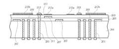
- FIG. 14A substrate with integrated passive devices formed in RDL layers and an UBM layer is shown according to the preferred embodiment of present invention.
- a substrate 200is provided with multiple through silicon vias (TSV) 201 penetrating therethrough.
- the TSV 201may be formed by first performing a laser drilling or a deep reactive ion etching (DRIE) process on the substrate 200 to form through holes, and then the through holes are filled up with conductive materials, such as Cu or W, to form TSV conductors.
- the TSV 201may include other components, such as an isolation layer, a barrier layer and/or a seed layer. Those additional components are omitted in the figures, for the simplicity and clarity of the description of the present invention.
- each dielectric layer 203 , 205may include a RDL layer which is electrically connected to the TSV 201 , wherein the RDL layer is composed of a 1st IPD 207 and RDL traces 209 .
- the dielectric layers 203 , 205may also include stacked vias 211 which are connected directly to the overlying solder bump 213 . The stacked vias 211 may make the TSV 201 longer so as to facilitate the connection of the TSV 201 to other dice on the substrate.
- a plurality of 2nd IPDsare formed on the topmost dielectric layer 205 , wherein the 2nd IPDs may be formed only from the UBM layer, such as a 2nd IPD 215 a , or the 2nd IPD may be formed by the bump filling material on the UBM layer, such as a 2nd IPD 215 b , That is, the 2nd IPD 215 b includes an upper bump layer and a lower UBM layer.
- the IPD pattern formed in/on the UBM levelsuch as the 2nd IPDs 215 a , 215 b , may or may not overlap the IPD pattern formed in the RDL levels, such as the 1st IPD 207 .
Landscapes
- Engineering & Computer Science (AREA)
- Computer Hardware Design (AREA)
- Microelectronics & Electronic Packaging (AREA)
- Power Engineering (AREA)
- Physics & Mathematics (AREA)
- Condensed Matter Physics & Semiconductors (AREA)
- General Physics & Mathematics (AREA)
- Manufacturing & Machinery (AREA)
- Internal Circuitry In Semiconductor Integrated Circuit Devices (AREA)
- Semiconductor Integrated Circuits (AREA)
Abstract
Description
- 1. Field of the Invention
- The present invention generally relates to a substrate with integrated passive devices. More particularly, the present invention is directed to form a substrate with integrated passive devices (IPD) in an under bump metallization (UBM) layer or redistribution layers (RDL).
- 2. Description of the Prior Art
- The rapid growth of the portable wireless electronics industry has provided numerous challenges and opportunities for the manufacturers of radio frequency (RF) components. The latest portable wireless telephony, data, and internet access products require greater functionalities, higher performances, and lower costs in smaller and lighter formats. These requirements have been partly satisfied through major advances in the integrated circuit (IC) device technology and by the introduction of smaller packaging form factors, smaller discrete passive components, and high-density interconnection printed circuit technologies.
- The RF sections of the portable wireless products are built with a range of active device technologies combined with high-performance passive components. As many as ninety-five percents of the components in a typical cellular telephone product may be passive devices. In a system using high-frequency electronic components or discrete passive devices, these discrete passive devices may occupy a large portion of the circuit board area and commensurately contribute to a large share of the product assembly costs. For this reason, the so-called integrated passive device (IPD) technology is developed to prevent the increase of the circuit size and of the high-frequency characteristics.
- The integrated passive devices (IPD) or the integrated passive components (IPC) are increasingly attracting due to constant needs of handheld wireless devices for further reduction in size and costs and for increase in functionalities. Many functional blocks, such as impedance matching circuits, harmonic filters, couplers, baluns or power combiners/dividers can be realized with IPD technologies. IPDs can be easily fabricated by using current conventional thin film processes and photolithography processes. They can also be designed as flip chip mountable or wire bondable components and are suitable to be fabricated on thin film substrates like silicon, glass or even on low temperature cofired ceramics (LTCC) multiplayer structures.
- The IPD technologies hold great potential for significantly reducing circuit board area as well as product size and weight, and/or for allowing increased functionalities in a given product size. The result is a high performance system level solution, which provides the advantages of reduction in die size, weight, number of interconnections and system board space requirements, and can be used in many applications.
- Yet challenges still remain in the field of further reduction of the IPD footprint and costs while concurrently simplifying fabrication processes and providing effective coupling and directionality. Accordingly, there is still a need for improving the design and the processes of the current IPD technology.
- To further improve the design of integrated passive device (IPD), a novel substrate with integrated passive devices and a method of manufacturing the same are presented in the present invention. The substrate of present invention may include multiple passive device patterns formed directly in different structural layers, such as in under bump metal (UBM) layers, intermediate dielectric layers or redistribution layers, or on the bonding pads of a substrate after a through silicon via (TSV) process. No additional Si interposer is necessary for disposing or forming the passive device patterns. The product size can therefore be effectively reduced. Furthermore, the passive device patterns in present invention may be formed concurrently during the patterning process of under bump metals and redistribution traces or during the filling process of stacked vias, thereby reducing the steps and costs for fabricating the passive device patterns on the substrate.
- One object of the present invention is to provide a substrate with integrated passive devices comprising a substrate, at least one dielectric layer formed on the substrate, a redistribution layer formed in each dielectric layer, an under bump metal layer formed on the dielectric layer, wherein the under bump metal layer comprises a first integrated passive device pattern, and bumps formed on the under bump metal layer.
- Another object of the present invention is to provide a substrate with integrated passive devices comprising a substrate, at least one dielectric layer formed on the substrate, a redistribution layer formed in each dielectric layer, wherein each redistribution layer comprises an integrated passive device pattern, redistribution traces and stacked vias, an under bump metal layer formed on the dielectric layer, and bumps formed on the under bump metal layer.
- Still another object of the present invention is to provide a method of manufacturing a substrate with integrated passive devices, comprising the steps of providing a substrate, forming a redistribution layer on the substrate, forming a dielectric layer on the redistribution layer, forming an under bump metal layer having a first integrated passive device pattern on the dielectric layer, and forming bumps on the under bump metal layer.
- Still another object of the present invention is to provide a method of manufacturing a substrate with integrated passive devices, comprising the steps of providing a substrate, forming at least one dielectric layer on the substrate, forming a redistribution layer having an integrated passive device pattern, redistribution traces and stacked vias in each dielectric layer, forming an under bump metal layer electrically connected with said stacked vias on the dielectric layer, and forming bumps on the under bump metal layer.
- These and other objectives of the present invention will no doubt become obvious to those of ordinary skill in the art after reading the following detailed description of the preferred embodiment that is illustrated in the various figures and drawings.
- The accompanying drawings are included to provide a further understanding of the embodiments, and are incorporated in and constitute apart of this specification. The drawings illustrate some of the embodiments and, together with the description, serve to explain their principles.
- In the drawings:
FIGS. 1-13 are cross-sectional views illustrating the process flow for manufacturing a substrate with integrated passive devices (IPD) formed in redistribution layers (RDL) and in an under bump metallization (UBM) in accordance with the second embodiment of the present invention;FIG. 14 is a cross-sectional view illustrating a substrate with integrated passive devices formed in redistribution layers and in an under bump metal in accordance with the first embodiment of the present invention.- It should be noted that all the figures are diagrammatic. Relative dimensions and proportions of parts of the drawings have been shown exaggerated or reduced in size, for the sake of clarity and convenience in the drawings. The same reference signs are generally used to refer to corresponding or similar features in modified and different embodiments.
- In following detailed description of the present invention, reference is made to the accompanying drawings which form a part hereof and is shown by way of illustration and specific embodiments in which the invention may be practiced. These embodiments are described in sufficient details to enable those skilled in the art to practice the invention. Other embodiments may be utilized and structural, logical, and electrical changes may be made without departing from the scope of the present invention.
- The embodiments will now be explained with reference to the accompanying drawings to provide a better understanding of the process of the present invention, wherein
FIGS. 1-13 are cross-sectional views illustrating the process flow for manufacturing said substrate with integrated passive devices, andFIG. 14 is a cross-sectional view illustrating an exemplary substrate with integrated passive devices manufactured through the process flow shown inFIGS. 1-13 . - First, please refer to
FIG. 1 , a substrate100 (ex. a wafer) is provided with an I/O pad 101, such as an Al pad, formed thereon. The I/O pad 101 is electrically connected to the interconnection circuits (ex. a top metal layer or a through silicon via (TSV)) inside thesubstrate 100 and is designed to be connected to an outer redistribution layer (RDL) for re-routing the positions of bond pads on the substrate. Alternatively, thesubstrate 100 may also be an interposer (ex. a substrate with through silicon vias (TSV) penetrating therethrough), like in the embodiment shown inFIG. 14 . In this application, each I/O pad 101 is connected to a TSV in the substrate instead of interconnection circuits. In the embodiment of present invention, thesubstrate 100 may be attached on a carrier (not shown) and the whole manufacturing process is performed on thebackside 100aof the substrate. The interconnection circuits and the TSV inside thesubstrate 100 will not be shown inFIG. 1 and other figures for purposes of clarity. - In the embodiment of present invention, the
substrate 100 may be a substrate suitable for thin-film processes and TSV processes, such as a silicon substrate, a glass substrate, a GaAs & sapphire (Al2O3) substrate, silicon-on-insulator (SOI), or even a chip or a Si interposer. The thin-film process is necessary in the present invention to manufacture integrated passive devices (IPD) on thesubstrate 100. The TSV process may be performed to connect multiplestacked substrates 100 for constructing a 3D-IC architecture by using, for example, wafer level package (WLP) technology. - Please refer again to
FIG. 1 . Anitride passivation 103 overlaps and seals the edges of the I/O pad 101, and adielectric layer 105 is deposited over thenitride passivation 103. A part of the I/O pad 101 is exposed from thedielectric layer 105 through anopening 107. Theopening 107 may be formed through a regular photolithographic processes including, for example, exposure and developing steps. In the embodiment of present invention, the material of thedielectric layer 105 may be polyimide (PI), poly-phenylene benzobisoxazole (PBO) or benzocyclobutene (BCB). The use of PI, PBO or BCB material can improve the stress relief of the redistribution layers (RDL) that will be formed on thedielectric layer 105 in following processes. An additional curing process may be performed to cure the depositeddielectric layer 105. - Subsequently, as shown in
FIG. 2 , ametallization layer 109 is formed on thesubstrate 100 to serve as a pre-layer for plating the RDL patterns. Themetallization layer 109 may be conformally formed on thesubstrate 100 through magnetron sputtering, e-beam evaporation, or electroless plating processes. Themetallization layer 109 is electrically connected with the underlying I/O pad 101 through theopening 107 of thedielectric layer 105. In the embodiment of present invention, themetallization layer 109 may be a film stack including Cr/CrCu/Cu, Ti(W)/Cu/Ni, Al/NiV/Cu or Ni/Au, which can meet the needs of adhesion, barrier, conductor, and protection properties. - After the
metallization layer 109 is formed, as shown inFIG. 3 , a patternedphotoresist layer 111 is coated on themetallization layer 109. Thephotoresist layer 111 serves as a block layer to prevent the formation of RDL patterns on undesired areas of thesubstrate 100 in following plating processes. In the embodiment of present invention, thephotoresist layer 111 includes a1st IPD pattern 111a, aRDL trace pattern 111band/or stacked via patterns (not shown), which may be obtained through a regular photo-lithographic process. Thesepatterns photoresist layer 111 which expose theunderlying metallization layer 109 inFIG. 3 . Thanks to the blocking of thephotoresist layer 111, desired patterns of conductive materials (ex. Cu or Au) for RDL may be readily formed on themetallization layer 109. - Thereafter, as shown in
FIG. 4 , an electroplating process is carried out to form aRDL layer 113 on the exposedmetallization layer 109 in thepatterns photoresist layer 111. In this figure, thephotoresist layer 111 has already been removed after the plating process and exposes theunderlying metallization layer 109. However, at this stage, the patterns of theRDL layer 113 are still connected by themetallization layer 109. To form individual RDL patterns, the exposedmetallization layer 109 should be disconnected. - Therefore, as shown in
FIG. 5 , a wet etching process is performed to remove the exposedmetallization layer 109. The removal of the exposedmetallization layer 109 divides the patterns of theRDL layer 113 into several individual conductive patterns, such as a1st IPD 113a, RDL traces113bor stacked vias (not shown). From a commodity technology initially developed to replace bulky discrete passive components, thin-film IPD are now a growing industry with a trend driven by ESD/EMI protections, RF, High brightness LEDs, and digital & mixed signal applications. The1st IPD 113amay be a passive device with the above-mentioned functions, such as a resistor, a capacitor, an inductor, a balun, a filter or a diplexer. In the embodiment of present invention, the1st IPD 113ais formed concurrently with the RDL traces113bduring the RDL process. This design may facilitate the manufacture of the IPD on the substrate with a thin-film technology. No additional layers or processes are required for forming the IPD in the present invention. - After the
IPD 113aand RDL traces113bare formed, as shown inFIG. 6 , adielectric layer 115 is formed on thesubstrate 100. A part of the RDL traces113bis exposed from thedielectric layer 115 through anopening 117. Similar toFIG. 1 , theopening 117 may be formed through regular photolithographic processes including, for example, exposure and developing steps. The material ofdielectric layer 115 may be polyimide (PI), poly-phenylene benzobisoxazole (PBO) or benzocyclobutene (BCB). - The re-routing
RDL trace 113bis designed to be connected to an outer bump. For this purpose, an under ball metallization (UBM) layer is needed to serve as an interface between the solder bump and theRDL trace 113b. As shown inFIG. 7 , aUBM layer 119 is formed on thesubstrate 100. TheUBM layer 119 may be conformally formed on thesubstrate 100 through magnetron sputtering, e-beam evaporation, or electroless plating processes. TheUBM layer 119 is electrically connected to theunderlying RDL trace 113bthrough theopening 117 of thedielectric layer 115. Similar to themetallization layer 109, in the present invention, theUBM layer 119 may be a film stack including materials such as Cr/CrCu/Cu, Ti(W)/Cu/Ni, Al/NiV/Cu or Ni/Au, which can meet the needs of adhesion, barrier, conductor, and protection properties. - After the
UBM layer 119 is formed on the substrate, as shown inFIG. 8 , a patternedphotoresist layer 121 is coated on theUBM layer 119. In the embodiment of present invention, thephotoresist layer 121 serves as a block layer to prevent the formation of bumps or IPD on undesired areas of thesubstrate 100. Thephotoresist layer 111 includes two2nd IPD patterns 121aand abump pattern 121b, which may be formed through a regular photolithographic process. Thesepatterns photoresist layer 121 and expose theunderlying UBM layer 119. Thanks to the blocking ofphotoresist layer 111, desired patterns of 2nd IPD and/or bump may be readily formed on theUBM layer 119. - Thereafter, as shown in
FIG. 9 , aconductive layer 123 is filled into thepatterns photoresist layer 111. In the embodiment of present invention, theconductive layer 123 may be formed on theUBM layer 119 through e-beam evaporation, electroplating or printing processes. The material of theconductive layer 123 may be Sn/Pb, Cu or Au. In this figure, thephotoresist layer 121 has already been removed after theconductive layer 123 is formed and exposes theunderlying UBM layer 119. However, at this stage, the patterns of the 2nd IDP and bumps are still connected with theUBM layer 119. To form individual IDP patterns and bumps, the exposedUBM layer 119 should be disconnected. - Therefore, as shown in
FIG. 10 , a wet etching process is performed using theconductive layer 123 as a mask to remove the exposedUBM layer 119. The removal of the exposedUBM layer 119 divides the patterns of theconductive layer 123 into a2nd IPD 123aand abump 123b. The2nd IPD 123amay be a passive device such as a resistor, a capacitor, an inductor, a balun, a filter or a diplexer. A final reflow process is then performed to shape thebump 123b. Thebump 123bmay be a solder bump, a micro bump or a C4 bump. - In the embodiment of present invention, the
2nd IPD 123ais formed concurrently with thesolder bump 123b. This design may facilitate the manufacturing process of the IPD on the substrate. No additional layers or processes are required to form the IPD in this invention. Furthermore, the2nd IPD 123aonUBM layer 119 may cooperate or correspond with theunderlying 1st IPD 113ain RDL layer. For example, in this embodiment, the right2nd IPD 123aon theUBM layer 119 overlaps the1st IPD 113a, thus the1st IPD 113a, thedielectric layer 115 and the2nd IPD 123amay constitute a capacitor passive device. Alternatively, the2nd IPD 123aonUBM layer 119 may be an individual IPD pattern. For example, the left2nd IPD 123adoesn't correspond to any IPD pattern in the underlying RDL layer. - Alternatively, in another embodiment of the present invention, the 2nd IPD may be formed by the patterning of
original UBM layer 119 instead of by filling the bump material into the patterns. In this embodiment, please refer toFIG. 11 , when theUBM layer 119 is formed on the substrate (as shown inFIG. 7 ), a patterned1st photoresist layer 125 is coated on theUBM layer 119. The predetermined areas for forming the 2nd IPD and the solder bump are covered by the1st photoresist layer 125, and the exposedUBM layer 119 is then removed through a wet etching process using the1st photoresist layer 125 as a mask. This etching process divides theUBM layer 119 into a thin2nd IPD 119aand abump portion 119b, as shown inFIG. 12 . The patterned2nd IPD 119ais then covered by a2nd photoresist layer 127 which exposes only thebump portion 119bof the UBM layer. The following process is similar to the steps shown inFIGS. 9-10 . A conductive layer is formed on thebump portion 119band is ref lowed into asolder bump 123b, as shown inFIG. 13 . Similar to the embodiment shown inFIG. 10 , the2nd IPD 119aofUBM layer 119 may or may not cooperate or correspond to the1st IPD pattern 113aof the underlying RDL layer. - In the present invention, the IPD components or patterns can be easily manufactured through RDL process, UBM process, and/or bump filling process in a regular process flow. Furthermore, since the IPD patterns are formed in the RDL layer, the UBM layer and/or the bump layer, the overall product size is not increased.
- Please refer now to
FIG. 14 . A substrate with integrated passive devices formed in RDL layers and an UBM layer is shown according to the preferred embodiment of present invention. As shown inFIG. 14 , asubstrate 200 is provided with multiple through silicon vias (TSV)201 penetrating therethrough. TheTSV 201 may be formed by first performing a laser drilling or a deep reactive ion etching (DRIE) process on thesubstrate 200 to form through holes, and then the through holes are filled up with conductive materials, such as Cu or W, to form TSV conductors. TheTSV 201 may include other components, such as an isolation layer, a barrier layer and/or a seed layer. Those additional components are omitted in the figures, for the simplicity and clarity of the description of the present invention. - Please refer again to
FIG. 14 . In this embodiment of present invention, at least one dielectric layer (ex.203 and205) is formed on thesubstrate 200. Eachdielectric layer TSV 201, wherein the RDL layer is composed of a1st IPD 207 and RDL traces209. Thedielectric layers stacked vias 211 which are connected directly to theoverlying solder bump 213. Thestacked vias 211 may make theTSV 201 longer so as to facilitate the connection of theTSV 201 to other dice on the substrate. A plurality of 2nd IPDs are formed on the topmostdielectric layer 205, wherein the 2nd IPDs may be formed only from the UBM layer, such as a2nd IPD 215a, or the 2nd IPD may be formed by the bump filling material on the UBM layer, such as a2nd IPD 215b, That is, the2nd IPD 215bincludes an upper bump layer and a lower UBM layer. For present invention, the IPD pattern formed in/on the UBM level, such as the2nd IPDs 1st IPD 207. - Those skilled in the art will readily observe that numerous modifications and alterations of the device and method may be made while retaining the teachings of the invention. Accordingly, the above disclosure should be construed as limited only by the metes and bounds of the appended claims.
Claims (20)
1. A substrate with integrated passive devices, comprising:
a substrate;
at least one dielectric layer formed on said substrate;
a redistribution layer formed in each said dielectric layer;
an under bump metal layer formed on said dielectric layer, wherein said under bump metal layer comprises a first integrated passive device pattern; and
bumps formed on said under bump metal layer.
2. The substrate with integrated passive devices according toclaim 1 , wherein said redistribution layer comprises a second integrated passive device pattern, redistribution traces and stacked vias.
3. The substrate with integrated passive devices according toclaim 2 , wherein said first integrated passive device pattern and said second integrated passive device pattern comprises resistors, capacitors, inductors, baluns, filters or diplexers.
4. The substrate with integrated passive devices according toclaim 1 , wherein said first integrated passive device pattern comprises under bump metal and bump metal.
5. The substrate with integrated passive devices according toclaim 1 , wherein said redistribution layer is electrically connected to a through silicon via in said substrate.
6. The substrate with integrated passive devices according toclaim 1 , wherein said dielectric layer, said redistribution layer and said under bump metal layer are formed on the backside of said substrate.
7. The substrate with integrated passive devices according toclaim 1 , wherein the material of said dielectric layer comprises polyimide (PI), poly-phenylene benzobisoxazole (PBO) or benzocyclobutene (BCB).
8. The substrate with integrated passive devices according toclaim 1 , wherein said substrate is a wafer level package substrate.
9. The substrate with integrated passive devices according toclaim 1 , wherein said bumps are solder bumps, micro bumps or C4 bumps.
10. A substrate with integrated passive devices, comprising:
a substrate;
at least one dielectric layer formed on said substrate;
a redistribution layer formed in each said dielectric layer, wherein each said redistribution layer comprises a integrated passive device pattern, redistribution traces and stacked vias;
an under bump metal layer formed on said dielectric layer; and
bumps formed on said under bump metal layer.
11. The substrate with integrated passive devices according toclaim 10 , wherein said dielectric layer, said redistribution layer and said under bump metal layer are formed on the backside of said substrate.
12. The substrate with integrated passive devices according toclaim 10 , wherein the material of said dielectric layer comprises polyimide (PI), poly-phenylene benzobisoxazole (PBO) or benzocyclobutene (BCB).
13. The substrate with integrated passive devices according toclaim 10 , wherein said integrated passive device pattern comprises resistors, capacitors, inductors, baluns, filters or diplexers.
14. The substrate with integrated passive devices according to claim10, wherein said bumps are solder bumps, micro bumps or C4 bumps.
15. A method of manufacturing a substrate with integrated passive devices, comprising the steps of:
providing a substrate;
forming a redistribution layer on said substrate;
forming a dielectric layer on said redistribution layer;
forming an under bump metal layer having a first integrated passive device pattern on said dielectric layer; and
forming bumps on said under bump metal layer.
16. The method of manufacturing a substrate with integrated passive devices accordingclaim 15 , wherein the step of forming an under bump metal having a first integrated passive device pattern comprises:
forming a under bump metal layer on said dielectric layer;
covering a photoresist with patterns of said first integrated passive device and said bumps on said under bump metal layer;
filling a bump material into said patterns of said under bump metal;
removing said photoresist; and
removing said exposed under bump layer.
17. The method of manufacturing a substrate with integrated passive devices accordingclaim 15 , wherein the step of forming an under bump metal having a first integrated passive device pattern comprises:
forming a under bump metal layer on said dielectric layer;
covering a first photoresist with patterns of said first integrated passive device and said bump on said under bump metal layer;
performing an etching process to remove the under bump metal layer which is not covered by said first photoresist so that said first integrated passive device pattern and a bump pattern of said under bump metal layer are formed;
removing said first photoresist;
covering a second photoresist which exposes only said bump pattern of said under bump metal layer
filling a bump material into said patterns of said under bump metal; and
removing said second photoresist.
18. The method of manufacturing a substrate with integrated passive devices accordingclaim 15 , wherein the step of forming a redistribution layer comprises:
forming a metallization layer on said substrate;
covering a photoresist with patterns of redistribution traces, stacked vias and a second integrated passive device on said metallization layer;
filling a RDL material into said patterns of redistribution traces and a second integrated passive device on said metallization layer;
removing said photoresist; and
removing said exposed metallization layer.
19. A method of manufacturing a substrate with integrated passive devices, comprising the steps of:
providing a substrate;
forming at least one dielectric layer on said substrate;
forming a redistribution layer having an integrated passive device pattern, redistribution traces and stacked vias in each said dielectric layer;
forming an under bump metal layer electrically connected to said stacked vias on said dielectric layer; and
forming bumps on said under bump metal layer.
20. The method of manufacturing a substrate with integrated passive devices accordingclaim 19 , wherein the step of forming a redistribution layer having an integrated passive device pattern and stacked vias comprises:
forming a metallization layer on said substrate;
covering a photoresist with patterns of said integrated passive device pattern and said stacked vias on said metallization layer;
plating a conductive material on said metallization layer in said patterns of said integrated passive device pattern and said stacked vias on said metallization layer;
removing said photoresist; and
removing exposed said metallization layer.
Priority Applications (1)
| Application Number | Priority Date | Filing Date | Title |
|---|---|---|---|
| US13/689,727US9035457B2 (en) | 2012-11-29 | 2012-11-29 | Substrate with integrated passive devices and method of manufacturing the same |
Applications Claiming Priority (1)
| Application Number | Priority Date | Filing Date | Title |
|---|---|---|---|
| US13/689,727US9035457B2 (en) | 2012-11-29 | 2012-11-29 | Substrate with integrated passive devices and method of manufacturing the same |
Publications (2)
| Publication Number | Publication Date |
|---|---|
| US20140145326A1true US20140145326A1 (en) | 2014-05-29 |
| US9035457B2 US9035457B2 (en) | 2015-05-19 |
Family
ID=50772533
Family Applications (1)
| Application Number | Title | Priority Date | Filing Date |
|---|---|---|---|
| US13/689,727Active2032-12-28US9035457B2 (en) | 2012-11-29 | 2012-11-29 | Substrate with integrated passive devices and method of manufacturing the same |
Country Status (1)
| Country | Link |
|---|---|
| US (1) | US9035457B2 (en) |
Cited By (29)
| Publication number | Priority date | Publication date | Assignee | Title |
|---|---|---|---|---|
| US8866024B1 (en)* | 2012-06-22 | 2014-10-21 | Altera Corporation | Transceiver power distribution network |
| US20150035162A1 (en)* | 2013-08-02 | 2015-02-05 | Qualcomm Incorporated | Inductive device that includes conductive via and metal layer |
| US20150228569A1 (en)* | 2014-02-07 | 2015-08-13 | Marvell World Trade Ltd. | Method and apparatus for improving the reliability of a connection to a via in a substrate |
| US20150235921A1 (en)* | 2014-02-20 | 2015-08-20 | Altera Corporation | Silicon-glass hybrid interposer circuitry |
| US9373594B2 (en)* | 2014-02-13 | 2016-06-21 | Taiwan Semiconductor Manufacturing Co., Ltd. | Under bump metallization |
| CN106099280A (en)* | 2016-08-22 | 2016-11-09 | 西安电子科技大学 | A kind of LC band filter based on the coupling electric capacity distribution of silicon through hole |
| US20180182717A1 (en)* | 2016-12-22 | 2018-06-28 | Nxp Usa, Inc. | Integrated circuit devices with selectively arranged through substrate vias and method of manufacture thereof |
| WO2020139951A1 (en)* | 2018-12-28 | 2020-07-02 | 3D Glass Solutions, Inc. | Heterogenous integration for rf, microwave and mm wave systems in photoactive glass substrates |
| US10854946B2 (en) | 2017-12-15 | 2020-12-01 | 3D Glass Solutions, Inc. | Coupled transmission line resonate RF filter |
| CN112234143A (en)* | 2020-12-14 | 2021-01-15 | 成都嘉纳海威科技有限责任公司 | On-chip integrated IPD packaging structure and packaging method thereof, and three-dimensional packaging structure |
| US10903545B2 (en) | 2018-05-29 | 2021-01-26 | 3D Glass Solutions, Inc. | Method of making a mechanically stabilized radio frequency transmission line device |
| US11076489B2 (en) | 2018-04-10 | 2021-07-27 | 3D Glass Solutions, Inc. | RF integrated power condition capacitor |
| CN113257842A (en)* | 2021-05-11 | 2021-08-13 | 上海芯波电子科技有限公司 | Semiconductor device and method for integrating passive device |
| US11101532B2 (en) | 2017-04-28 | 2021-08-24 | 3D Glass Solutions, Inc. | RF circulator |
| CN113410221A (en)* | 2021-06-16 | 2021-09-17 | 上海芯波电子科技有限公司 | Multiplexer integrating acoustic mechanical wave device and passive device |
| US11139582B2 (en) | 2018-09-17 | 2021-10-05 | 3D Glass Solutions, Inc. | High efficiency compact slotted antenna with a ground plane |
| US11161773B2 (en) | 2016-04-08 | 2021-11-02 | 3D Glass Solutions, Inc. | Methods of fabricating photosensitive substrates suitable for optical coupler |
| US11177065B2 (en)* | 2020-03-30 | 2021-11-16 | Qualcomm Incorporated | Thermal paths for glass substrates |
| US11264167B2 (en) | 2016-02-25 | 2022-03-01 | 3D Glass Solutions, Inc. | 3D capacitor and capacitor array fabricating photoactive substrates |
| US11270964B2 (en)* | 2016-10-12 | 2022-03-08 | International Business Machines Corporation | Mixed UBM and mixed pitch on a single die |
| US11270843B2 (en) | 2018-12-28 | 2022-03-08 | 3D Glass Solutions, Inc. | Annular capacitor RF, microwave and MM wave systems |
| US11342896B2 (en) | 2017-07-07 | 2022-05-24 | 3D Glass Solutions, Inc. | 2D and 3D RF lumped element devices for RF system in a package photoactive glass substrates |
| US11373908B2 (en) | 2019-04-18 | 2022-06-28 | 3D Glass Solutions, Inc. | High efficiency die dicing and release |
| CN115663424A (en)* | 2022-09-06 | 2023-01-31 | 中国电子科技集团公司第二十九研究所 | A RF filter based on silicon-based integrated product development |
| US11677373B2 (en) | 2018-01-04 | 2023-06-13 | 3D Glass Solutions, Inc. | Impedence matching conductive structure for high efficiency RF circuits |
| US11908617B2 (en) | 2020-04-17 | 2024-02-20 | 3D Glass Solutions, Inc. | Broadband induction |
| US11929199B2 (en) | 2014-05-05 | 2024-03-12 | 3D Glass Solutions, Inc. | 2D and 3D inductors fabricating photoactive substrates |
| US11962057B2 (en) | 2019-04-05 | 2024-04-16 | 3D Glass Solutions, Inc. | Glass based empty substrate integrated waveguide devices |
| US12165809B2 (en) | 2016-02-25 | 2024-12-10 | 3D Glass Solutions, Inc. | 3D capacitor and capacitor array fabricating photoactive substrates |
Families Citing this family (9)
| Publication number | Priority date | Publication date | Assignee | Title |
|---|---|---|---|---|
| US9171798B2 (en) | 2013-01-25 | 2015-10-27 | Taiwan Semiconductor Manufacturing Company, Ltd. | Methods and apparatus for transmission lines in packages |
| US10068181B1 (en) | 2015-04-27 | 2018-09-04 | Rigetti & Co, Inc. | Microwave integrated quantum circuits with cap wafer and methods for making the same |
| US11121301B1 (en) | 2017-06-19 | 2021-09-14 | Rigetti & Co, Inc. | Microwave integrated quantum circuits with cap wafers and their methods of manufacture |
| US11276727B1 (en) | 2017-06-19 | 2022-03-15 | Rigetti & Co, Llc | Superconducting vias for routing electrical signals through substrates and their methods of manufacture |
| EP3890612A4 (en) | 2018-12-06 | 2022-10-05 | Analog Devices, Inc. | Shielded integrated device packages |
| WO2020118031A1 (en) | 2018-12-06 | 2020-06-11 | Analog Devices, Inc. | Integrated device packages with passive device assemblies |
| KR20210011279A (en) | 2019-07-22 | 2021-02-01 | 삼성전자주식회사 | Semiconductor package |
| US20210159182A1 (en)* | 2019-11-22 | 2021-05-27 | Taiwan Semiconductor Manufacturing Co., Ltd. | Semiconductor Devices and Methods of Manufacture |
| US11664340B2 (en) | 2020-07-13 | 2023-05-30 | Analog Devices, Inc. | Negative fillet for mounting an integrated device die to a carrier |
Citations (2)
| Publication number | Priority date | Publication date | Assignee | Title |
|---|---|---|---|---|
| US20110115050A1 (en)* | 2009-11-19 | 2011-05-19 | Stats Chippac, Ltd. | Semiconductor Device and Method of Forming IPD on Molded Substrate |
| US20120228754A1 (en)* | 2011-03-08 | 2012-09-13 | Georgia Tech Research Corporation | Chip-last embedded interconnect structures and methods of making the same |
Family Cites Families (103)
| Publication number | Priority date | Publication date | Assignee | Title |
|---|---|---|---|---|
| DE1514818A1 (en) | 1951-01-28 | 1969-05-08 | Telefunken Patent | Solid-state circuit, consisting of a semiconductor body with inserted active components and an insulating layer with applied passive components and conductor tracks |
| US3150299A (en) | 1959-09-11 | 1964-09-22 | Fairchild Camera Instr Co | Semiconductor circuit complex having isolation means |
| US3256465A (en) | 1962-06-08 | 1966-06-14 | Signetics Corp | Semiconductor device assembly with true metallurgical bonds |
| US3343256A (en) | 1964-12-28 | 1967-09-26 | Ibm | Methods of making thru-connections in semiconductor wafers |
| US3323198A (en) | 1965-01-27 | 1967-06-06 | Texas Instruments Inc | Electrical interconnections |
| US3372070A (en) | 1965-07-30 | 1968-03-05 | Bell Telephone Labor Inc | Fabrication of semiconductor integrated devices with a pn junction running through the wafer |
| US3648131A (en) | 1969-11-07 | 1972-03-07 | Ibm | Hourglass-shaped conductive connection through semiconductor structures |
| US4394712A (en) | 1981-03-18 | 1983-07-19 | General Electric Company | Alignment-enhancing feed-through conductors for stackable silicon-on-sapphire wafers |
| US4395302A (en) | 1981-12-10 | 1983-07-26 | Enthone Incorporated | Metal dissolution process using H2 O2 --H2 SO4 etchant |
| US4616247A (en) | 1983-11-10 | 1986-10-07 | At&T Bell Laboratories | P-I-N and avalanche photodiodes |
| KR900008647B1 (en) | 1986-03-20 | 1990-11-26 | 후지쓰 가부시끼가이샤 | A method for manufacturing three demensional i.c. |
| US4773972A (en) | 1986-10-30 | 1988-09-27 | Ford Motor Company | Method of making silicon capacitive pressure sensor with glass layer between silicon wafers |
| US5463246A (en) | 1988-12-29 | 1995-10-31 | Sharp Kabushiki Kaisha | Large scale high density semiconductor apparatus |
| US5399898A (en) | 1992-07-17 | 1995-03-21 | Lsi Logic Corporation | Multi-chip semiconductor arrangements using flip chip dies |
| US5229647A (en) | 1991-03-27 | 1993-07-20 | Micron Technology, Inc. | High density data storage using stacked wafers |
| JP3004071B2 (en) | 1991-04-16 | 2000-01-31 | 日本特殊陶業株式会社 | Package for integrated circuit |
| US5214000A (en) | 1991-12-19 | 1993-05-25 | Raychem Corporation | Thermal transfer posts for high density multichip substrates and formation method |
| US5372969A (en) | 1991-12-31 | 1994-12-13 | Texas Instruments Incorporated | Low-RC multi-level interconnect technology for high-performance integrated circuits |
| EP0721662A1 (en) | 1993-09-30 | 1996-07-17 | Kopin Corporation | Three-dimensional processor using transferred thin film circuits |
| US5484073A (en) | 1994-03-28 | 1996-01-16 | I/O Sensors, Inc. | Method for fabricating suspension members for micromachined sensors |
| US5502333A (en) | 1994-03-30 | 1996-03-26 | International Business Machines Corporation | Semiconductor stack structures and fabrication/sparing methods utilizing programmable spare circuit |
| US5627106A (en) | 1994-05-06 | 1997-05-06 | United Microelectronics Corporation | Trench method for three dimensional chip connecting during IC fabrication |
| AU5084998A (en) | 1996-11-08 | 1998-05-29 | W.L. Gore & Associates, Inc. | Method for using photoabsorptive coatings to enhance both blind and through micro-via entrance quality |
| US6551857B2 (en) | 1997-04-04 | 2003-04-22 | Elm Technology Corporation | Three dimensional structure integrated circuits |
| US6143616A (en) | 1997-08-22 | 2000-11-07 | Micron Technology, Inc. | Methods of forming coaxial integrated circuitry interconnect lines |
| US6309956B1 (en) | 1997-09-30 | 2001-10-30 | Intel Corporation | Fabricating low K dielectric interconnect systems by using dummy structures to enhance process |
| US5977640A (en) | 1998-06-26 | 1999-11-02 | International Business Machines Corporation | Highly integrated chip-on-chip packaging |
| US20010038972A1 (en) | 1998-11-20 | 2001-11-08 | Christopher F. Lyons | Ultra-thin resist shallow trench process using metal hard mask |
| US6162587A (en) | 1998-12-01 | 2000-12-19 | Advanced Micro Devices | Thin resist with transition metal hard mask for via etch application |
| US6274937B1 (en) | 1999-02-01 | 2001-08-14 | Micron Technology, Inc. | Silicon multi-chip module packaging with integrated passive components and method of making |
| US6573565B2 (en) | 1999-07-28 | 2003-06-03 | International Business Machines Corporation | Method and structure for providing improved thermal conduction for silicon semiconductor devices |
| US6483147B1 (en) | 1999-10-25 | 2002-11-19 | Advanced Micro Devices, Inc. | Through wafer backside contact to improve SOI heat dissipation |
| US6633083B2 (en) | 2000-02-28 | 2003-10-14 | Advanced Micro Devices Inc. | Barrier layer integrity test |
| JP4023076B2 (en) | 2000-07-27 | 2007-12-19 | 富士通株式会社 | Front and back conductive substrate and manufacturing method thereof |
| US6407002B1 (en) | 2000-08-10 | 2002-06-18 | Taiwan Semiconductor Manufacturing Company | Partial resist free approach in contact etch to improve W-filling |
| JP2002134658A (en) | 2000-10-24 | 2002-05-10 | Shinko Electric Ind Co Ltd | Semiconductor device and its manufacturing method |
| US6805614B2 (en) | 2000-11-30 | 2004-10-19 | Texas Instruments Incorporated | Multilayered CMP stop for flat planarization |
| US6391777B1 (en) | 2001-05-02 | 2002-05-21 | Taiwan Semiconductor Manufacturing Company | Two-stage Cu anneal to improve Cu damascene process |
| US6812193B2 (en) | 2001-08-31 | 2004-11-02 | International Business Machines Corporation | Slurry for mechanical polishing (CMP) of metals and use thereof |
| US6831013B2 (en) | 2001-11-13 | 2004-12-14 | United Microelectronics Corp. | Method of forming a dual damascene via by using a metal hard mask layer |
| US6627985B2 (en) | 2001-12-05 | 2003-09-30 | Arbor Company Llp | Reconfigurable processor module comprising hybrid stacked integrated circuit die elements |
| US7126214B2 (en) | 2001-12-05 | 2006-10-24 | Arbor Company Llp | Reconfigurable processor module comprising hybrid stacked integrated circuit die elements |
| US6525419B1 (en) | 2002-02-14 | 2003-02-25 | Intel Corporation | Thermally coupling electrically decoupling cooling device for integrated circuits |
| US6778275B2 (en) | 2002-02-20 | 2004-08-17 | Micron Technology, Inc. | Aberration mark and method for estimating overlay error and optical aberrations |
| US6800930B2 (en) | 2002-07-31 | 2004-10-05 | Micron Technology, Inc. | Semiconductor dice having back side redistribution layer accessed using through-silicon vias, and assemblies |
| US6930048B1 (en) | 2002-09-18 | 2005-08-16 | Lam Research Corporation | Etching a metal hard mask for an integrated circuit structure |
| JP2004140286A (en) | 2002-10-21 | 2004-05-13 | Nec Semiconductors Kyushu Ltd | Semiconductor device and its manufacturing method |
| KR100480897B1 (en) | 2002-12-09 | 2005-04-07 | 매그나칩 반도체 유한회사 | Method for manufacturing STI of semiconductor device |
| WO2004075319A1 (en) | 2003-02-20 | 2004-09-02 | Mitsubishi Chemical Corporation | Active substance for negative electrode of lithium secondary battery, negative electrode of lithium secondary battery and lithium secondary battery |
| US7449780B2 (en) | 2003-03-31 | 2008-11-11 | Intel Corporation | Apparatus to minimize thermal impedance using copper on die backside |
| US6897148B2 (en) | 2003-04-09 | 2005-05-24 | Tru-Si Technologies, Inc. | Electroplating and electroless plating of conductive materials into openings, and structures obtained thereby |
| US6924551B2 (en) | 2003-05-28 | 2005-08-02 | Intel Corporation | Through silicon via, folded flex microelectronic package |
| US7111149B2 (en) | 2003-07-07 | 2006-09-19 | Intel Corporation | Method and apparatus for generating a device ID for stacked devices |
| US7083495B2 (en) | 2003-11-26 | 2006-08-01 | Taiwan Semiconductor Manufacturing Company, Ltd. | Advanced process control approach for Cu interconnect wiring sheet resistance control |
| US7049170B2 (en) | 2003-12-17 | 2006-05-23 | Tru-Si Technologies, Inc. | Integrated circuits and packaging substrates with cavities, and attachment methods including insertion of protruding contact pads into cavities |
| US7060601B2 (en) | 2003-12-17 | 2006-06-13 | Tru-Si Technologies, Inc. | Packaging substrates for integrated circuits and soldering methods |
| US7420277B2 (en) | 2004-03-16 | 2008-09-02 | Taiwan Semiconductor Manufacturing Company, Ltd | System for heat dissipation in semiconductor devices |
| JP4439976B2 (en) | 2004-03-31 | 2010-03-24 | Necエレクトロニクス株式会社 | Semiconductor device and manufacturing method thereof |
| US7075133B1 (en) | 2004-05-03 | 2006-07-11 | National Semiconductor Corporation | Semiconductor die with heat and electrical pipes |
| TWI237316B (en) | 2004-08-24 | 2005-08-01 | Chipmos Technologies Inc | Electronic device having pin electrode with slight warpage |
| US7098070B2 (en) | 2004-11-16 | 2006-08-29 | International Business Machines Corporation | Device and method for fabricating double-sided SOI wafer scale package with through via connections |
| US7396732B2 (en) | 2004-12-17 | 2008-07-08 | Interuniversitair Microelektronica Centrum Vzw (Imec) | Formation of deep trench airgaps and related applications |
| JP4577687B2 (en) | 2005-03-17 | 2010-11-10 | エルピーダメモリ株式会社 | Semiconductor device |
| US7166913B2 (en) | 2005-04-19 | 2007-01-23 | International Business Machines Corporation | Heat dissipation for heat generating element of semiconductor device and related method |
| US7402515B2 (en) | 2005-06-28 | 2008-07-22 | Intel Corporation | Method of forming through-silicon vias with stress buffer collars and resulting devices |
| US7432592B2 (en) | 2005-10-13 | 2008-10-07 | Intel Corporation | Integrated micro-channels for 3D through silicon architectures |
| US7410884B2 (en) | 2005-11-21 | 2008-08-12 | Intel Corporation | 3D integrated circuits using thick metal for backside connections and offset bumps |
| US20070126085A1 (en) | 2005-12-02 | 2007-06-07 | Nec Electronics Corporation | Semiconductor device and method of manufacturing the same |
| JP2007165461A (en) | 2005-12-12 | 2007-06-28 | Elpida Memory Inc | Semiconductor device and manufacturing method thereof |
| US7563714B2 (en) | 2006-01-13 | 2009-07-21 | International Business Machines Corporation | Low resistance and inductance backside through vias and methods of fabricating same |
| US7427803B2 (en) | 2006-09-22 | 2008-09-23 | Taiwan Semiconductor Manufacturing Company, Ltd. | Electromagnetic shielding using through-silicon vias |
| US8026169B2 (en) | 2006-11-06 | 2011-09-27 | Advanced Micro Devices, Inc. | Cu annealing for improved data retention in flash memory devices |
| US7795735B2 (en) | 2007-03-21 | 2010-09-14 | Taiwan Semiconductor Manufacturing Co., Ltd. | Methods for forming single dies with multi-layer interconnect structures and structures formed therefrom |
| US7564115B2 (en) | 2007-05-16 | 2009-07-21 | Taiwan Semiconductor Manufacturing Company, Ltd. | Tapered through-silicon via structure |
| KR101336569B1 (en) | 2007-05-22 | 2013-12-03 | 삼성전자주식회사 | Semiconductor Packages With Enhanced Joint Reliability And Methods Of Fabricating The Same |
| US7939941B2 (en) | 2007-06-27 | 2011-05-10 | Taiwan Semiconductor Manufacturing Company, Ltd. | Formation of through via before contact processing |
| US7825517B2 (en) | 2007-07-16 | 2010-11-02 | Taiwan Semiconductor Manufacturing Company, Ltd. | Method for packaging semiconductor dies having through-silicon vias |
| KR101341586B1 (en) | 2007-08-30 | 2013-12-16 | 삼성전자주식회사 | Semiconductor integrated circuit device and fabricating method of the same |
| JP2009129953A (en) | 2007-11-20 | 2009-06-11 | Hitachi Ltd | Semiconductor device |
| US20090127667A1 (en) | 2007-11-21 | 2009-05-21 | Powertech Technology Inc. | Semiconductor chip device having through-silicon-via (TSV) and its fabrication method |
| US7843064B2 (en) | 2007-12-21 | 2010-11-30 | Taiwan Semiconductor Manufacturing Company, Ltd. | Structure and process for the formation of TSVs |
| KR101420817B1 (en) | 2008-01-15 | 2014-07-21 | 삼성전자주식회사 | Semiconductor integrated circuit device for electrically connecting stacked integrated circuit modules with three-dimensional serial and parallel circuits and method of forming the device |
| US8486823B2 (en) | 2008-03-07 | 2013-07-16 | Taiwan Semiconductor Manufacturing Co., Ltd. | Methods of forming through via |
| US7812426B2 (en) | 2008-05-30 | 2010-10-12 | Taiwan Semiconductor Manufacturing Company, Ltd. | TSV-enabled twisted pair |
| KR20100003911A (en) | 2008-07-02 | 2010-01-12 | 삼성전자주식회사 | Multi-chip package having three dimension mesh-based power distribution network and power distribution method thereof |
| US7851346B2 (en) | 2008-07-21 | 2010-12-14 | Taiwan Semiconductor Manufacturing Company, Ltd. | Bonding metallurgy for three-dimensional interconnect |
| KR20100021856A (en) | 2008-08-18 | 2010-02-26 | 삼성전자주식회사 | Method of forming semiconductor device having tsv and related device |
| US7846837B2 (en) | 2008-10-09 | 2010-12-07 | United Microelectronics Corp. | Through substrate via process |
| US7956442B2 (en) | 2008-10-09 | 2011-06-07 | Taiwan Semiconductor Manufacturing Company, Ltd. | Backside connection to TSVs having redistribution lines |
| US7928534B2 (en) | 2008-10-09 | 2011-04-19 | Taiwan Semiconductor Manufacturing Company, Ltd. | Bond pad connection to redistribution lines having tapered profiles |
| US8053900B2 (en) | 2008-10-21 | 2011-11-08 | Taiwan Semiconductor Manufacturing Company, Ltd. | Through-substrate vias (TSVs) electrically connected to a bond pad design with reduced dishing effect |
| US7955895B2 (en) | 2008-11-07 | 2011-06-07 | Taiwan Semiconductor Manufacturing Co., Ltd. | Structure and method for stacked wafer fabrication |
| US7825024B2 (en) | 2008-11-25 | 2010-11-02 | Taiwan Semiconductor Manufacturing Company, Ltd. | Method of forming through-silicon vias |
| US8053902B2 (en) | 2008-12-02 | 2011-11-08 | Taiwan Semiconductor Manufacturing Company, Ltd. | Isolation structure for protecting dielectric layers from degradation |
| US8168470B2 (en) | 2008-12-08 | 2012-05-01 | Stats Chippac, Ltd. | Semiconductor device and method of forming vertical interconnect structure in substrate for IPD and baseband circuit separated by high-resistivity molding compound |
| US8227889B2 (en) | 2008-12-08 | 2012-07-24 | United Microelectronics Corp. | Semiconductor device |
| US8049327B2 (en) | 2009-01-05 | 2011-11-01 | Taiwan Semiconductor Manufacturing Company, Ltd. | Through-silicon via with scalloped sidewalls |
| US7932608B2 (en) | 2009-02-24 | 2011-04-26 | Taiwan Semiconductor Manufacturing Company, Ltd. | Through-silicon via formed with a post passivation interconnect structure |
| US8329578B2 (en) | 2009-03-27 | 2012-12-11 | Taiwan Semiconductor Manufacturing Company, Ltd. | Via structure and via etching process of forming the same |
| US8202766B2 (en) | 2009-06-19 | 2012-06-19 | United Microelectronics Corp. | Method for fabricating through-silicon via structure |
| US8053898B2 (en) | 2009-10-05 | 2011-11-08 | Samsung Electronics Co., Ltd. | Connection for off-chip electrostatic discharge protection |
| US8618629B2 (en) | 2009-10-08 | 2013-12-31 | Qualcomm Incorporated | Apparatus and method for through silicon via impedance matching |
| US7969013B2 (en) | 2009-10-22 | 2011-06-28 | Taiwan Semiconductor Manufacturing Company, Ltd. | Through silicon via with dummy structure and method for forming the same |
- 2012
- 2012-11-29USUS13/689,727patent/US9035457B2/enactiveActive
Patent Citations (2)
| Publication number | Priority date | Publication date | Assignee | Title |
|---|---|---|---|---|
| US20110115050A1 (en)* | 2009-11-19 | 2011-05-19 | Stats Chippac, Ltd. | Semiconductor Device and Method of Forming IPD on Molded Substrate |
| US20120228754A1 (en)* | 2011-03-08 | 2012-09-13 | Georgia Tech Research Corporation | Chip-last embedded interconnect structures and methods of making the same |
Cited By (39)
| Publication number | Priority date | Publication date | Assignee | Title |
|---|---|---|---|---|
| US8937258B1 (en)* | 2012-06-22 | 2015-01-20 | Altera Corporation | Transceiver power distribution network |
| US8866024B1 (en)* | 2012-06-22 | 2014-10-21 | Altera Corporation | Transceiver power distribution network |
| US20150035162A1 (en)* | 2013-08-02 | 2015-02-05 | Qualcomm Incorporated | Inductive device that includes conductive via and metal layer |
| US9659851B2 (en)* | 2014-02-07 | 2017-05-23 | Marvell World Trade Ltd. | Method and apparatus for improving the reliability of a connection to a via in a substrate |
| US20150228569A1 (en)* | 2014-02-07 | 2015-08-13 | Marvell World Trade Ltd. | Method and apparatus for improving the reliability of a connection to a via in a substrate |
| US9373594B2 (en)* | 2014-02-13 | 2016-06-21 | Taiwan Semiconductor Manufacturing Co., Ltd. | Under bump metallization |
| US10134694B2 (en) | 2014-02-13 | 2018-11-20 | Taiwan Semiconductor Manufacturing Company, Ltd. | Method of forming redistribution layer |
| US20150235921A1 (en)* | 2014-02-20 | 2015-08-20 | Altera Corporation | Silicon-glass hybrid interposer circuitry |
| US9425125B2 (en)* | 2014-02-20 | 2016-08-23 | Altera Corporation | Silicon-glass hybrid interposer circuitry |
| US11929199B2 (en) | 2014-05-05 | 2024-03-12 | 3D Glass Solutions, Inc. | 2D and 3D inductors fabricating photoactive substrates |
| US12165809B2 (en) | 2016-02-25 | 2024-12-10 | 3D Glass Solutions, Inc. | 3D capacitor and capacitor array fabricating photoactive substrates |
| US11264167B2 (en) | 2016-02-25 | 2022-03-01 | 3D Glass Solutions, Inc. | 3D capacitor and capacitor array fabricating photoactive substrates |
| US11161773B2 (en) | 2016-04-08 | 2021-11-02 | 3D Glass Solutions, Inc. | Methods of fabricating photosensitive substrates suitable for optical coupler |
| CN106099280A (en)* | 2016-08-22 | 2016-11-09 | 西安电子科技大学 | A kind of LC band filter based on the coupling electric capacity distribution of silicon through hole |
| US11270964B2 (en)* | 2016-10-12 | 2022-03-08 | International Business Machines Corporation | Mixed UBM and mixed pitch on a single die |
| US20180182717A1 (en)* | 2016-12-22 | 2018-06-28 | Nxp Usa, Inc. | Integrated circuit devices with selectively arranged through substrate vias and method of manufacture thereof |
| US10574198B2 (en)* | 2016-12-22 | 2020-02-25 | Nxp Usa, Inc. | Integrated circuit devices with selectively arranged through substrate vias and method of manufacture thereof |
| US11101532B2 (en) | 2017-04-28 | 2021-08-24 | 3D Glass Solutions, Inc. | RF circulator |
| US11342896B2 (en) | 2017-07-07 | 2022-05-24 | 3D Glass Solutions, Inc. | 2D and 3D RF lumped element devices for RF system in a package photoactive glass substrates |
| US10854946B2 (en) | 2017-12-15 | 2020-12-01 | 3D Glass Solutions, Inc. | Coupled transmission line resonate RF filter |
| US11894594B2 (en) | 2017-12-15 | 2024-02-06 | 3D Glass Solutions, Inc. | Coupled transmission line resonate RF filter |
| US11367939B2 (en) | 2017-12-15 | 2022-06-21 | 3D Glass Solutions, Inc. | Coupled transmission line resonate RF filter |
| US11677373B2 (en) | 2018-01-04 | 2023-06-13 | 3D Glass Solutions, Inc. | Impedence matching conductive structure for high efficiency RF circuits |
| US11076489B2 (en) | 2018-04-10 | 2021-07-27 | 3D Glass Solutions, Inc. | RF integrated power condition capacitor |
| US10903545B2 (en) | 2018-05-29 | 2021-01-26 | 3D Glass Solutions, Inc. | Method of making a mechanically stabilized radio frequency transmission line device |
| US11139582B2 (en) | 2018-09-17 | 2021-10-05 | 3D Glass Solutions, Inc. | High efficiency compact slotted antenna with a ground plane |
| WO2020139951A1 (en)* | 2018-12-28 | 2020-07-02 | 3D Glass Solutions, Inc. | Heterogenous integration for rf, microwave and mm wave systems in photoactive glass substrates |
| US11270843B2 (en) | 2018-12-28 | 2022-03-08 | 3D Glass Solutions, Inc. | Annular capacitor RF, microwave and MM wave systems |
| JP2022511230A (en)* | 2018-12-28 | 2022-01-31 | スリーディー グラス ソリューションズ,インク | Heterogeneous integration for RF, microwave and MM wave systems on photoactive glass substrates |
| US11594457B2 (en) | 2018-12-28 | 2023-02-28 | 3D Glass Solutions, Inc. | Heterogenous integration for RF, microwave and MM wave systems in photoactive glass substrates |
| JP7241433B2 (en) | 2018-12-28 | 2023-03-17 | スリーディー グラス ソリューションズ,インク | Heterogeneous Integration for RF, Microwave and MM Wave Systems on Photoactive Glass Substrates |
| US11962057B2 (en) | 2019-04-05 | 2024-04-16 | 3D Glass Solutions, Inc. | Glass based empty substrate integrated waveguide devices |
| US11373908B2 (en) | 2019-04-18 | 2022-06-28 | 3D Glass Solutions, Inc. | High efficiency die dicing and release |
| US11177065B2 (en)* | 2020-03-30 | 2021-11-16 | Qualcomm Incorporated | Thermal paths for glass substrates |
| US11908617B2 (en) | 2020-04-17 | 2024-02-20 | 3D Glass Solutions, Inc. | Broadband induction |
| CN112234143A (en)* | 2020-12-14 | 2021-01-15 | 成都嘉纳海威科技有限责任公司 | On-chip integrated IPD packaging structure and packaging method thereof, and three-dimensional packaging structure |
| CN113257842A (en)* | 2021-05-11 | 2021-08-13 | 上海芯波电子科技有限公司 | Semiconductor device and method for integrating passive device |
| CN113410221A (en)* | 2021-06-16 | 2021-09-17 | 上海芯波电子科技有限公司 | Multiplexer integrating acoustic mechanical wave device and passive device |
| CN115663424A (en)* | 2022-09-06 | 2023-01-31 | 中国电子科技集团公司第二十九研究所 | A RF filter based on silicon-based integrated product development |
Also Published As
| Publication number | Publication date |
|---|---|
| US9035457B2 (en) | 2015-05-19 |
Similar Documents
| Publication | Publication Date | Title |
|---|---|---|
| US9035457B2 (en) | Substrate with integrated passive devices and method of manufacturing the same | |
| US20220189884A1 (en) | Formation method of chip package | |
| CN102623391B (en) | Semiconductor device with on a semiconductor die square become the method for integrated passive devices | |
| KR101965035B1 (en) | Wireless charging package with chip integrated in coil center | |
| US8125055B2 (en) | Packaging technology | |
| US9147660B2 (en) | Chip to package interface | |
| CN102290329B (en) | Form semiconductor device and the method with the RF FEM of LC filter and IPD filter | |
| US9209148B2 (en) | Semiconductor package | |
| US20060220173A1 (en) | Wafer level package including a device wafer integrated with a passive component | |
| EP2107599B1 (en) | Method Of Forming A Wafer Level Package | |
| EP1636843A1 (en) | Package for a high-frequency electronic device | |
| US10861841B2 (en) | Semiconductor device with multiple polarity groups | |
| US11395408B2 (en) | Wafer-level passive array packaging | |
| US12272862B2 (en) | Antenna apparatus and fabrication method | |
| JP3540729B2 (en) | Semiconductor device and manufacturing method of semiconductor device | |
| CN120545254A (en) | Semiconductor device and method of manufacturing semiconductor device | |
| CN112563229A (en) | Semiconductor package and method of manufacturing the same | |
| TWI498996B (en) | Semiconductor component and method of forming an inductor on a trench filled with insulating material in a substrate | |
| JP2008135753A (en) | Multichip electronic circuit module, and method for manufacturing the same | |
| KR20130077565A (en) | Semiconductor package and method of manufacturing the same | |
| TW202412248A (en) | Integrated package and method for making the same | |
| JP4380551B2 (en) | Semiconductor device and manufacturing method thereof | |
| US11258162B1 (en) | Antenna package and method of formation thereof | |
| JP4591100B2 (en) | Semiconductor device and manufacturing method thereof | |
| US11842993B2 (en) | Semiconductor device with multiple polarity groups |
Legal Events
| Date | Code | Title | Description |
|---|---|---|---|
| AS | Assignment | Owner name:UNITED MICROELECTRONICS CORP., TAIWAN Free format text:ASSIGNMENT OF ASSIGNORS INTEREST;ASSIGNORS:LIN, CHU-FU;LIN, MING-TSE;LIN, YUNG-CHANG;REEL/FRAME:029377/0809 Effective date:20121126 | |
| AS | Assignment | Owner name:HERCULES TECHNOLOGY GROWTH CAPITAL, INC., CALIFORN Free format text:SECURITY AGREEMENT;ASSIGNOR:OCZ TECHNOLOGY GROUP, INC.;REEL/FRAME:030092/0739 Effective date:20130311 | |
| STCF | Information on status: patent grant | Free format text:PATENTED CASE | |
| MAFP | Maintenance fee payment | Free format text:PAYMENT OF MAINTENANCE FEE, 4TH YEAR, LARGE ENTITY (ORIGINAL EVENT CODE: M1551); ENTITY STATUS OF PATENT OWNER: LARGE ENTITY Year of fee payment:4 | |
| MAFP | Maintenance fee payment | Free format text:PAYMENT OF MAINTENANCE FEE, 8TH YEAR, LARGE ENTITY (ORIGINAL EVENT CODE: M1552); ENTITY STATUS OF PATENT OWNER: LARGE ENTITY Year of fee payment:8 |